WO2023120158A1 - 防汚層付き光学フィルムおよびその製造方法 - Google Patents
防汚層付き光学フィルムおよびその製造方法 Download PDFInfo
- Publication number
- WO2023120158A1 WO2023120158A1 PCT/JP2022/044872 JP2022044872W WO2023120158A1 WO 2023120158 A1 WO2023120158 A1 WO 2023120158A1 JP 2022044872 W JP2022044872 W JP 2022044872W WO 2023120158 A1 WO2023120158 A1 WO 2023120158A1
- Authority
- WO
- WIPO (PCT)
- Prior art keywords
- film
- layer
- antifouling layer
- optical film
- antifouling
- Prior art date
- Legal status (The legal status is an assumption and is not a legal conclusion. Google has not performed a legal analysis and makes no representation as to the accuracy of the status listed.)
- Ceased
Links
Images



Classifications
-
- B—PERFORMING OPERATIONS; TRANSPORTING
- B32—LAYERED PRODUCTS
- B32B—LAYERED PRODUCTS, i.e. PRODUCTS BUILT-UP OF STRATA OF FLAT OR NON-FLAT, e.g. CELLULAR OR HONEYCOMB, FORM
- B32B37/00—Methods or apparatus for laminating, e.g. by curing or by ultrasonic bonding
- B32B37/02—Methods or apparatus for laminating, e.g. by curing or by ultrasonic bonding characterised by a sequence of laminating steps, e.g. by adding new layers at consecutive laminating stations
-
- B—PERFORMING OPERATIONS; TRANSPORTING
- B05—SPRAYING OR ATOMISING IN GENERAL; APPLYING FLUENT MATERIALS TO SURFACES, IN GENERAL
- B05D—PROCESSES FOR APPLYING FLUENT MATERIALS TO SURFACES, IN GENERAL
- B05D1/00—Processes for applying liquids or other fluent materials
- B05D1/28—Processes for applying liquids or other fluent materials performed by transfer from the surfaces of elements carrying the liquid or other fluent material, e.g. brushes, pads, rollers
-
- B—PERFORMING OPERATIONS; TRANSPORTING
- B05—SPRAYING OR ATOMISING IN GENERAL; APPLYING FLUENT MATERIALS TO SURFACES, IN GENERAL
- B05D—PROCESSES FOR APPLYING FLUENT MATERIALS TO SURFACES, IN GENERAL
- B05D5/00—Processes for applying liquids or other fluent materials to surfaces to obtain special surface effects, finishes or structures
- B05D5/06—Processes for applying liquids or other fluent materials to surfaces to obtain special surface effects, finishes or structures to obtain multicolour or other optical effects
-
- B—PERFORMING OPERATIONS; TRANSPORTING
- B32—LAYERED PRODUCTS
- B32B—LAYERED PRODUCTS, i.e. PRODUCTS BUILT-UP OF STRATA OF FLAT OR NON-FLAT, e.g. CELLULAR OR HONEYCOMB, FORM
- B32B27/00—Layered products comprising a layer of synthetic resin
-
- C—CHEMISTRY; METALLURGY
- C08—ORGANIC MACROMOLECULAR COMPOUNDS; THEIR PREPARATION OR CHEMICAL WORKING-UP; COMPOSITIONS BASED THEREON
- C08J—WORKING-UP; GENERAL PROCESSES OF COMPOUNDING; AFTER-TREATMENT NOT COVERED BY SUBCLASSES C08B, C08C, C08F, C08G or C08H
- C08J7/00—Chemical treatment or coating of shaped articles made of macromolecular substances
- C08J7/04—Coating
-
- B—PERFORMING OPERATIONS; TRANSPORTING
- B05—SPRAYING OR ATOMISING IN GENERAL; APPLYING FLUENT MATERIALS TO SURFACES, IN GENERAL
- B05D—PROCESSES FOR APPLYING FLUENT MATERIALS TO SURFACES, IN GENERAL
- B05D2252/00—Sheets
- B05D2252/02—Sheets of indefinite length
-
- B—PERFORMING OPERATIONS; TRANSPORTING
- B32—LAYERED PRODUCTS
- B32B—LAYERED PRODUCTS, i.e. PRODUCTS BUILT-UP OF STRATA OF FLAT OR NON-FLAT, e.g. CELLULAR OR HONEYCOMB, FORM
- B32B2255/00—Coating on the layer surface
- B32B2255/10—Coating on the layer surface on synthetic resin layer or on natural or synthetic rubber layer
-
- B—PERFORMING OPERATIONS; TRANSPORTING
- B32—LAYERED PRODUCTS
- B32B—LAYERED PRODUCTS, i.e. PRODUCTS BUILT-UP OF STRATA OF FLAT OR NON-FLAT, e.g. CELLULAR OR HONEYCOMB, FORM
- B32B2255/00—Coating on the layer surface
- B32B2255/28—Multiple coating on one surface
Definitions
- the present invention relates to an optical film with an antifouling layer and a method for producing the same.
- an optical film with an antifouling layer is attached to the outer surface of a display such as a touch panel display on the image display side.
- An optical film with an antifouling layer includes a transparent substrate film and an antifouling layer disposed on the outermost surface on one side of the transparent substrate film.
- the antifouling layer suppresses adhesion of contaminants such as oil from hands to the outer surface of the display, and facilitates removal of the adhering contaminants.
- An optical film with an antifouling layer is manufactured, for example, by a roll-to-roll method from the viewpoint of manufacturing efficiency.
- the antifouling layer forming step in the roll-to-roll method for example, while running a long transparent base film as a work film along the pass line in the same process, the base material is removed at a predetermined location in the pass line.
- An antifouling layer is formed on one side in the thickness direction of the film.
- the antifouling layer is formed from a highly water-repellent material by, for example, a wet coating method or a dry coating method.
- the optical film with an antifouling layer (having an antifouling layer on its surface) is wound up by a take-up roller.
- the antifouling layer on the outermost surface on one side of the transparent substrate film is in contact with the other side (back surface) of the same film.
- a load is applied in the film thickness direction (roll radial direction).
- the present inventors have obtained the following findings regarding the optical film with an antifouling layer produced as described above.
- the antifouling layer material is easily transferred from the antifouling layer to the back surface of the transparent substrate film. This problem is particularly likely to occur when the antifouling layer is formed by a dry coating method. In addition, the above problem is more likely to occur as the antifouling layer formed is thicker.
- the present invention provides a method for producing an optical film with an antifouling layer, which can produce an optical film with an antifouling layer by a roll-to-roll method while preventing the adhesion of an antifouling layer material to the back surface of a transparent base film, and an antifouling film.
- a method for producing an optical film with an antifouling layer which can produce an optical film with an antifouling layer by a roll-to-roll method while preventing the adhesion of an antifouling layer material to the back surface of a transparent base film, and an antifouling film.
- the present invention [1] comprises an antifouling layer forming step of forming an antifouling layer on one side in the thickness direction of the transparent base film while conveying the transparent base film by a roll-to-roll method; Before the dirt layer forming step or before winding the transparent base film with the dirt resistant layer after the dirt layer forming step, the other side in the thickness direction of the transparent base film is protected. It includes a method for producing an optical film with an antifouling layer, including a step of laminating films.
- a composite film comprising a transparent base film and a protective film laminated on one side of the transparent base film is conveyed by roll-to-roll, and the protective film in the transparent base film and the includes a method for producing an optical film with an antifouling layer, which includes an antifouling layer forming step for forming an antifouling layer on the opposite side.
- the present invention [3] includes the method for producing an optical film with an antifouling layer according to [1] or [2] above, wherein in the antifouling layer forming step, the antifouling layer is formed by a dry coating method.
- the present invention [4] is the optical film with an antifouling layer according to any one of [1] to [3] above, wherein the surface free energy of the other surface in the thickness direction of the protective film is 45 mN/m or less. including the manufacturing method of
- the present invention [5] includes the method for producing an optical film with an antifouling layer according to any one of [1] to [4] above, wherein the antifouling layer has a thickness of 6 nm or more.
- the present invention [6] comprises a transparent substrate film, an antifouling layer disposed on one side in the thickness direction of the transparent substrate film, and an antifouling layer disposed on the other side in the thickness direction of the transparent substrate film. and a protective film.
- the present invention [7] includes the optical film with an antifouling layer according to [6] above, wherein the antifouling layer is a dry coating film.
- the present invention [8] includes the optical film with an antifouling layer according to [6] or [7] above, wherein the antifouling layer has a thickness of 6 nm or more.
- the present invention [9] is the optical film with an antifouling layer according to any one of [6] to [8] above, wherein the surface free energy of the other surface in the thickness direction of the protective film is 45 mN/m or less. including.
- the transparent substrate film with an antifouling layer is wound before the antifouling layer forming step or after the antifouling layer forming step.
- a lamination step is included before.
- a protective film is bonded to the other side in the thickness direction of the transparent substrate film.
- the antifouling layer is formed on the transparent base film side of the composite film (the transparent base film having a protective film on one side). Therefore, according to these production methods, it is possible to produce an optical film with an antifouling layer by a roll-to-roll method while preventing the adhesion of the antifouling layer material to the back surface of the transparent base film by the protective film.
- the optical film with an antifouling layer of the present invention comprises a transparent base film, an antifouling layer disposed on one side in the thickness direction of the same film, and the other side in the thickness direction of the transparent base film. and a protective film disposed on the side.
- Such an optical film with an antifouling layer can be produced by a roll-to-roll method while preventing adhesion of the antifouling layer material to the back surface of the transparent base film.
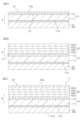
- FIG. 1A shows a step of preparing a transparent substrate film
- FIG. 1B shows a step of forming a hard coat layer
- FIG. 1C shows an example of a bonding step.
- 2A shows the step of forming the adhesion layer
- FIG. 2B shows the step of forming the antireflection layer
- FIG. 2C shows the step of forming the antifouling layer.
- a modification of the bonding process is represented. It represents one modification of the optical film with an antifouling layer of the present invention. In this modified example, no antireflection layer is provided.
- FIG. 1 and 2 are process diagrams of one embodiment of the method for producing an optical film with an antifouling layer of the present invention.
- the method for producing an optical film with an antifouling layer includes a preparation step (FIG. 1A), a hard coat layer forming step (FIG. 1B), a bonding step (FIG. 1C), and an adhesion layer forming step (FIG. 2A), an antireflection layer forming step (FIG. 2B), and an antifouling layer forming step (FIG. 2C).
- a preparation step FIG. 1A
- FIG. 1B hard coat layer forming step
- FIG. 1C a bonding step
- FIG. 2A an adhesion layer forming step
- FIG. 2B an antireflection layer forming step
- FIG. 2C antifouling layer forming step
- a resin film 11 is prepared as shown in FIG. 1A.
- the resin film 11 has a long shape so that this manufacturing method can be carried out by a roll-to-roll system.
- the resin film 11 has a front surface 11a and a back surface 11b opposite to the front surface 11a.
- the resin film 11 is a flexible transparent resin film.
- materials for the resin film 11 include polyester resin, polyolefin resin, polystyrene resin, acrylic resin, polycarbonate resin, polyethersulfone resin, polysulfone resin, polyamide resin, polyimide resin, cellulose resin, norbornene resin, polyarylate resin, and A polyvinyl alcohol resin is mentioned.
- Polyester resins include, for example, polyethylene terephthalate (PET), polybutylene terephthalate, and polyethylene naphthalate.
- Polyolefin resins include, for example, polyethylene, polypropylene, and cycloolefin polymers (COP).
- Cellulose resins include, for example, triacetyl cellulose (TAC).
- the material for the resin film 11 one selected from the group consisting of polyester resin, polyolefin resin, and cellulose resin is used from the viewpoint of transparency and strength, and more preferably the group consisting of PET, COP, and TAC. A more selected one is used.
- the surface 11a of the resin film 11 may be subjected to a surface modification treatment.
- Surface modification treatments include, for example, corona treatment, plasma treatment, ozone treatment, primer treatment, glow treatment, and coupling agent treatment.
- the thickness of the resin film 11 is preferably 5 ⁇ m or more, more preferably 10 ⁇ m or more, and even more preferably 20 ⁇ m or more.
- the thickness of the resin film 11 is preferably 300 ⁇ m or less, more preferably 200 ⁇ m or less, from the viewpoint of handleability.
- the total light transmittance (JIS K 7375-2008) of the resin film 11 is preferably 80% or higher, more preferably 90% or higher, still more preferably 95% or higher. Such a configuration is suitable for ensuring the transparency required for the optical film when the optical film is provided on the surface of a display such as a touch panel display.
- the total light transmittance of the resin film 11 is, for example, 100% or less.
- a hard coat layer 12 is formed on the resin film 11 as shown in FIG. 1B.
- the transparent substrate film 10 including the resin film 11 and the hard coat layer 12 is obtained.
- the hard coat layer 12 forms one surface (surface 10a) in the thickness direction D of the transparent base film 10 .
- the hard coat layer 12 is a layer for making it difficult for scratches to form on the exposed surface of the optical film F (the upper surface in the figure for the optical film F shown in FIG. 2C).
- a hard-coat layer formation process is implemented by a roll-to-roll system in this embodiment.
- the hard coat layer 12 can be formed, for example, by applying a curable resin composition (varnish) on the surface 11a of the resin film 11 to form a coating film, and then drying and curing the coating film.
- a curable resin composition contains a curable resin and a solvent.
- the hard coat layer 12 is a cured product of a curable resin composition (specifically, a curable resin).
- curable resins examples include polyester resins, acrylic resins, urethane resins, acrylic urethane resins, amide resins, silicone resins, epoxy resins, and melamine resins. These curable resins may be used alone, or two or more of them may be used in combination. From the viewpoint of ensuring high hardness of the hard coat layer 12, acrylic urethane resin is preferably used as the curable resin.
- curable resins include ultraviolet curable resins and thermosetting resins.
- the coating film is cured by ultraviolet irradiation.
- the curable resin composition contains a thermosetting resin, the coating film is cured by heating.
- an ultraviolet curable resin is preferably used from the viewpoint of improving the production efficiency of the optical film F because it can be cured without heating to a high temperature.
- the UV-curable resin includes at least one selected from the group consisting of UV-curable monomers, UV-curable oligomers, and UV-curable polymers. Specific examples of the composition containing an ultraviolet curable resin include the composition for forming a hard coat layer described in JP-A-2016-179686.
- Solvents contained in the curable resin composition include, for example, ethyl acetate, butyl acetate, acetone, methyl ethyl ketone, methyl isobutyl ketone, benzene, toluene, xylene, methanol, ethanol, isopropanol, ethylene glycol monomethyl ether acetate, propylene glycol monomethyl ether. Acetate, dichloromethane, and chloroform are included.
- the curable resin composition may contain fine particles.
- the addition of fine particles to the curable resin composition is useful for adjusting the hardness, adjusting the surface roughness, adjusting the refractive index, and imparting antiglare properties of the hard coat layer 12 .
- Microparticles include, for example, metal oxide particles, glass particles, and organic particles.
- Materials for metal oxide particles include, for example, silica, alumina, titania, zirconia, calcium oxide, tin oxide, indium oxide, cadmium oxide, and antimony oxide.
- Materials for the organic particles include, for example, polymethylmethacrylate, polystyrene, polyurethane, acrylic-styrene copolymers, benzoguanamine, melamine, and polycarbonate.
- the thickness of the hard coat layer 12 is preferably 1 ⁇ m or more, more preferably 3 ⁇ m or more, and even more preferably 5 ⁇ m, from the viewpoint of ensuring the hardness of the surface 23a of the antifouling layer 23 described later by ensuring the hardness of the hard coat layer 12. That's it. From the viewpoint of ensuring the flexibility of the optical film F, the thickness of the hard coat layer 12 is preferably 50 ⁇ m or less, more preferably 40 ⁇ m or less, still more preferably 35 ⁇ m or less, and particularly preferably 30 ⁇ m or less.
- a surface 12a (the surface on which the adhesion layer 21 described later is laminated) as one surface in the thickness direction D of the hard coat layer 12 is subjected to a surface modification treatment as necessary.
- Surface modification treatments include, for example, plasma treatment, corona treatment, ozone treatment, primer treatment, glow treatment, and coupling agent treatment.
- the surface 12a is preferably plasma-treated.
- argon gas for example, is used as an inert gas.
- the discharge power in the plasma treatment is, for example, 10 W or more and, for example, 10000 W or less.
- a protective film 30 is bonded to the other surface (back surface 10b) of the transparent substrate film 10 in the thickness direction D by a roll-to-roll bonding machine. (Lamination process).
- the protective film 30 includes a base film 31 and an adhesive layer 32 in this embodiment.
- the adhesive layer 32 side of the protective film 30 is attached to the back surface 10 b of the transparent base film 10 .
- a long roll-shaped composite film 100 including the transparent base film 10 and the protective film 30 is obtained.
- the base film 31 has a first surface 31a and a second surface 31b opposite to the first surface 31a.
- the base film 31 is, for example, a flexible resin film.
- resin film materials include polyolefin, polyester, polyvinyl chloride, polyvinylidene chloride, cellulose, polystyrene, and polycarbonate.
- Polyolefins include, for example, polyethylene, polypropylene, ethylene/propylene copolymers, ethylene/vinyl acetate copolymers, and ethylene/vinyl alcohol copolymers.
- Polyesters include, for example, polyethylene terephthalate, polyethylene naphthalate, and polybutylene terephthalate.
- the thickness of the base film 31 is, for example, 12 ⁇ m or more, preferably 25 ⁇ m or more, and is, for example, 200 ⁇ m or less, preferably 150 ⁇ m or less.
- the adhesive layer 32 is formed on the first surface 31 a of the base film 31 .
- the adhesive layer 32 contains a base polymer that allows the adhesive layer 32 to exhibit adhesiveness.
- base polymers include acrylic polymers, rubber-based polymers, polyester-based polymers, urethane-based polymers, polyether-based polymers, silicone-based polymers, polyamide-based polymers, and fluorine-based polymers.
- the thickness of the adhesive layer 32 is, for example, 5 ⁇ m or more, preferably 10 ⁇ m or more, and is, for example, 100 ⁇ m or less, preferably 75 ⁇ m or less.
- the other surface of the protective film 30 in the thickness direction D may be subjected to transfer suppression treatment.
- the transfer suppressing treatment include attaching a lubricant to the second surface 31b and forming a resin layer (transfer suppressing layer) containing the lubricant.
- Lubricants include, for example, wax esters, natural waxes containing the wax esters, silicone-based lubricants, and fluorine-based lubricants.
- Wax esters are, for example, esters of higher fatty acids and higher alcohols.
- Wax esters include, for example, myricyl cerotate, myricyl palmitate, cetyl palmitate, and stearyl stearate.
- Natural waxes containing wax esters include, for example, vegetable waxes and animal waxes. Vegetable waxes include, for example, carnauba wax (containing myricyl cerotinate as a main component) and palm wax.
- Animal waxes include, for example, beeswax and spermaceti.
- silicone-based lubricants include dimethylpolysiloxane and modified products thereof, carboxyl-modified silicone, ⁇ -methylstyrene-modified silicone, ⁇ -olefin-modified silicone, polyether-modified silicone, epoxy-modified silicone, amino-modified silicone, amide-modified silicone, and alcohol-modified silicones;
- the transfer suppressing layer forms the second surface 31 b of the protective film 30 .
- the transfer suppressing layer can be formed, for example, by applying a curable resin composition (varnish) on the second surface 31b of the base film 31 to form a coating film, and then drying and curing the coating film.
- the curable resin composition for forming the transfer suppressing layer contains, for example, a curable resin, the lubricant described above, and a solvent, and if necessary, other components such as an antistatic agent.
- the transfer suppressing layer is a cured product of such a curable resin composition.
- the curable resin and solvent include, for example, the curable resins and solvents described above for the hard coat layer 12 .
- the content of the lubricant in the transfer suppressing layer is preferably 5% by mass or more, more preferably 8% by mass or more, from the viewpoint of appropriately controlling the surface free energy of the second surface 31b of the protective film 30, for example, within the range described later. , more preferably 10% by mass or more, preferably 50% by mass or less, more preferably 45% by mass or less, and still more preferably 40% by mass or less.
- wax esters and natural waxes containing the wax esters are preferred because they are less likely to whiten even under hot and humid conditions. It is important for films that require optical transparency that components in the transfer inhibiting layer are resistant to whitening.
- the transfer suppressing layer preferably contains an antistatic agent. Containing an antistatic agent in the transfer suppressing layer is preferable for imparting antistatic properties to the optical film F and suppressing adhesion of foreign matter to the optical film F.
- Antistatic agents include, for example, organic antistatic agents and inorganic antistatic agents.
- Organic antistatic agents include, for example, cationic antistatic agents (having cationic functional groups such as quaternary ammonium salts, pyridinium salts, primary amino groups, secondary amino groups, and tertiary amino groups), and anionic antistatic agents.
- Antistatic agents having anionic functional groups such as sulfonates, sulfates, phosphonates, and phosphates), zwitterionic antistatic agents (alkylbetaine and its derivatives, imidazoline and its derivatives, alanine and its derivatives, etc.), nonionic antistatic agents (aminoalcohol and its derivatives, glycerin and its derivatives, polyethylene glycol and its derivatives, etc.), and conductive polymers.
- Conductive polymers include, for example, polythiophene, polyaniline, polypyrrole, polyethyleneimine, and allylamine.
- inorganic antistatic agents include tin oxide, antimony oxide, indium oxide, cadmium oxide, titanium oxide, zinc oxide, indium, tin, antimony, gold, silver, copper, aluminum, nickel, chromium, titanium, iron, cobalt , copper iodide, indium-tin composite oxide (ITO), and antimony-tin composite oxide (ATO).
- the content of the antistatic agent in the transfer suppressing layer is preferably 0.03% by mass or more, more preferably 0.05% by mass or more, and still more preferably 0.1% by mass, from the viewpoint of ensuring good antistatic properties. or more, preferably 10% by mass or less, more preferably 5% by mass or less.
- the thickness of the transfer suppressing layer is preferably 1 nm or more, more preferably 3 nm or more, and even more preferably 5 nm or more, from the viewpoint of appropriately controlling the surface free energy of the second surface 31b of the protective film 30 within the range described later. .
- the thickness of the transfer suppressing layer is preferably 1000 nm or less, more preferably 500 nm or less, and even more preferably 100 nm or less, from the viewpoints of ensuring good appearance of the optical film F and suppressing manufacturing costs.
- the surface free energy of the second surface 31b of the protective film 30 is 45 mN/m or less, preferably 43 mN/m or less, more preferably 40 mN/m or less. Surface free energy is measured by the method described below with respect to the examples. The lower the surface free energy of the second surface 31b, the lower the affinity between the second surface 31b and the antifouling layer material such as an organic fluorine compound having a fluorinated alkyl group at its terminal.
- the surface free energy of the second surface 31b of the protective film 30 is, for example, 15 mN/m or more from the viewpoint of appropriately conveying the composite film 100 (work film) in the roll-to-roll manufacturing process, preferably It is 20 mN/m or more, more preferably 25 mN/m or more, and still more preferably 30 mN/m or more.
- ⁇ d is the dispersive component of the surface free energy
- ⁇ p is the polar component of the surface free energy
- ⁇ h is the hydrogen bonding component of the surface free energy.
- the method for obtaining the surface free energy is as described later with regard to Examples.
- the adhesion layer 21 is a layer for ensuring adhesion of the inorganic oxide layer (antireflection layer 22 described later in this embodiment) to the organic layer (hard coat layer 12 in this embodiment).
- materials for the adhesion layer 21 include metals such as silicon, nickel, chromium, aluminum, tin, gold, silver, platinum, zinc, titanium, tungsten, zirconium, and palladium, and alloys of two or more of these metals. , and oxides of these metals.
- the adhesion layer 21 Indium tin oxide (ITO) or silicon oxide (SiOx) is preferably used as the material of .
- ITO Indium tin oxide
- SiOx silicon oxide
- SiOx with less oxygen content than the stoichiometric composition is used, and more preferably SiOx with x of 1.2 or more and 1.9 or less is used.
- the adhesion layer 21 is formed, for example, by depositing a material using a dry coating method. Dry coating methods include sputtering, vacuum deposition, and CVD, with sputtering being preferred.
- a negative voltage is applied to the target placed on the cathode while gas is introduced into the sputtering chamber under vacuum conditions.
- glow discharge is generated to ionize the gas atoms, and the gas ions collide with the target surface at high speed, ejecting the target material from the target surface and depositing the ejected target material on a predetermined surface.
- Reactive sputtering is preferable as the sputtering method from the viewpoint of film formation rate.
- a metal target is used as the target, and a mixed gas of an inert gas such as argon and oxygen (reactive gas) is used as the above gas.
- Examples of power sources for carrying out the sputtering method include DC power sources, AC power sources, RF power sources, and MFAC power sources (AC power sources with a frequency band of several kHz to several MHz).
- the discharge voltage in the sputtering method is, for example, 200 V or higher and, for example, 1000 V or lower.
- the film forming pressure in the sputtering chamber where the sputtering method is performed is preferably 0.01 Pa or higher, more preferably 0.05 Pa or higher, and even more preferably 0.1 Pa or higher.
- the film formation pressure is, for example, 2 Pa or less from the viewpoint of discharge stability.
- the thickness of the adhesion layer 21 is preferably 1 nm or more and 10 nm or less from the viewpoint of ensuring both the adhesion between the hard coat layer 12 and the antireflection layer 22 and the transparency of the adhesion layer 21 .
- the antireflection layer 22 is formed on one surface of the adhesion layer 21 in the thickness direction D.
- the antireflection layer 22 is a layer for suppressing the reflection intensity of external light.
- the antireflection layer 22 has high refractive index layers with a relatively high refractive index and low refractive index layers with a relatively low refractive index alternately in the thickness direction.
- the net reflected light intensity is attenuated by interference between reflected light at multiple interfaces in multiple thin layers (high refractive index layer, low refractive index layer) included in the same layer.
- the optical film thickness the product of the refractive index and the thickness
- such antireflection layer 22 in the present embodiment includes a first high refractive index layer 22a, a first low refractive index layer 22b, a second high refractive index layer 22c, and a second low refractive index layer 22c. and a layer 22d in this order toward one side in the thickness direction D.
- the first high refractive index layer 22a, the first low refractive index layer 22b, the second high refractive index layer 22c, and the second low refractive index layer 22d can each be formed by depositing materials using a dry coating method. Dry coating methods include sputtering, vacuum deposition, and CVD, with sputtering being preferred. As the sputtering method, reactive sputtering is preferable from the viewpoint of film formation speed.
- the conditions of the sputtering method in this step are the same as those described above as the conditions of the sputtering method in the adhesion layer forming step.
- Each of the first high refractive index layer 22a and the second high refractive index layer 22c is made of a high refractive index material having a refractive index of preferably 1.9 or more at a wavelength of 550 nm.
- high refractive index materials include niobium oxide (Nb 2 O 5 ), titanium oxide, zirconium oxide, indium tin oxide (ITO), and Antimony tin oxide (ATO) is mentioned, preferably niobium oxide is used.
- the optical film thickness (product of refractive index and thickness) of the first high refractive index layer 22a is, for example, 20 nm or more and, for example, 55 nm or less.
- the optical film thickness of the second high refractive index layer 22c is, for example, 60 nm or more and is, for example, 330 nm or less.
- Each of the first low refractive index layer 22b and the second low refractive index layer 22d is made of a low refractive index material having a refractive index of preferably 1.6 or less at a wavelength of 550 nm.
- low refractive index materials include, for example, silicon dioxide (SiO 2 ) and magnesium fluoride, preferably silicon dioxide.
- the optical film thickness of the first low refractive index layer 22b is, for example, 15 nm or more and, for example, 70 nm or less.
- the optical film thickness of the second low refractive index layer 22d is, for example, 100 nm or more and is, for example, 160 nm or less.
- the antifouling layer 23 is formed on one surface of the antireflection layer 22 in the thickness direction D by a roll-to-roll method.
- the antifouling layer 23 is a layer having an antifouling function.
- the antifouling function of the antifouling layer 30 includes a function of suppressing adhesion of contaminants such as oil from hands to the exposed surface (upper surface in the figure) of the optical film F, and a function of facilitating removal of adhering contaminants. .
- the antifouling layer 23 is formed by depositing an antifouling layer material on the antireflection layer 22 by a dry coating method. That is, the antifouling layer 23 is a film (dry coating film) formed by a dry coating method. Dry coating methods include, for example, vacuum deposition, sputtering, and CVD.
- the antifouling layer 23 is preferably a film (vacuum vapor deposition film) formed by a vacuum vapor deposition method.
- the structure in which the antifouling layer 23 is a dry coating film (preferably a vacuum deposition film) is suitable for ensuring high bonding strength of the antifouling layer 23 to the base, and therefore suitable for ensuring the peeling resistance of the antifouling layer 23. .
- the high antifouling property of the antifouling layer 23 helps to maintain the antifouling function of the antifouling layer 23 .
- an organic fluorine compound having a fluorinated alkyl group at its terminal is preferably used as the material for the antifouling layer 23.
- the organic fluorine compound is suitable for exhibiting excellent antifouling properties in the antifouling layer 23 by superimposing high hydrophobicity and high oleophobicity due to the terminal fluorinated alkyl group.
- an alkoxysilane compound having a perfluoropolyether group represented by the following general formula (1) is preferably used.
- R 1 represents a linear or branched fluorinated alkyl group (having, for example, 1 or more and 20 or less carbon atoms) in which one or more hydrogen atoms in the alkyl group are substituted with fluorine atoms. preferably represents a perfluoroalkyl group in which all hydrogen atoms in an alkyl group are substituted with fluorine atoms.
- R 2 represents a structure containing at least one repeating structure of perfluoropolyether (PFPE) groups, preferably a structure containing two repeating structures of PFPE groups.
- PFPE groups include repeating structures of linear PFPE groups and repeating structures of branched PFPE groups.
- the repeating structure of the linear PFPE group for example, a structure represented by -(OC n F 2n ) p - (n represents an integer of 1 or more and 20 or less, p represents an integer of 1 or more and 50 or less The same applies below).
- the repeating structure of the branched PFPE group for example, a structure represented by -(OC(CF 3 ) 2 ) p - and a structure represented by -(OCF 2 CF(CF 3 )CF 2 ) p - is mentioned.
- the repeating structure of the PFPE group preferably includes a repeating structure of a linear PFPE group, more preferably -(OCF 2 ) p - and -(OC 2 F 4 ) p -.
- R 3 represents an alkyl group having 1 to 4 carbon atoms, preferably a methyl group.
- X represents an ether group, a carbonyl group, an amino group, or an amide group, preferably an ether group.
- n represents an integer of 1 or more.
- m represents an integer of preferably 20 or less, more preferably 10 or less, and even more preferably 5 or less.
- alkoxysilane compounds having a perfluoropolyether group compounds represented by the following general formula (2) are preferably used.
- q represents an integer of 1 or more and 50 or less
- r represents an integer of 1 or more and 50 or less
- alkoxysilane compound having a perfluoropolyether group may be used alone, or two or more of them may be used in combination.
- the thickness of the antifouling layer 23 is preferably 6 nm or more, more preferably 7 nm or more, from the viewpoint of ensuring the antifouling property of the antifouling layer 23 .
- the thickness of the antifouling layer 23 is preferably 25 nm or less, more preferably 20 nm or less, and even more preferably 18 nm or less from the viewpoint of suppressing peeling of the antifouling layer material.
- a series of processes from the adhesion layer forming step to the antifouling layer forming step are carried out in one pass line while conveying the work film by a roll-to-roll method.
- the work film is never exposed to the atmosphere.
- the work film is wound up by a winding roller arranged at the end of the pass line.
- the transparent base material with the antifouling layer 23 is formed after the antifouling layer forming step by the roll-to-roll method. It may be performed before the film 10 is wound.
- FIG. 3 schematically represents an example of such a laminating step after the antifouling layer forming step.
- the work film W that has undergone the preparation step (FIG. 1A), the hard coat layer forming step (FIG. 1B), the adhesion layer forming step (FIG. 2A), and the antireflection layer forming step (FIG. 2B) is rolled to roll. transported by the method.
- the long roll-shaped protective film 30 is attached to the delivery roller 202, and the protective film 30 is directed from the protective film roll to the rollers 203, 203 of the roll-to-roll laminating machine. is being brought out.
- the work film W undergoes film formation (antifouling layer forming step) of the antifouling layer material 201 by a dry coating method, and is laminated with the protective film 30 before being wound up by the winding roller 204. combining process).
- the adhesive layer 32 side of the protective film 30 is bonded to the back surface 10b of the transparent base film 10 of the work film W by the rollers 203,203.
- the optical film F as the work film W is wound around the winding roller 204 .
- the optical film F is manufactured as described above.
- the optical film F includes a protective film 30, a transparent substrate film 10, an adhesion layer 21, an antireflection layer 22, and an antifouling layer 23 in this order toward one side in the thickness direction D.
- the optical film F has a shape that spreads in a direction perpendicular to the thickness direction D (plane direction).
- the optical film F is used after the protective film 30 is peeled off from the transparent substrate film 10, and then the transparent substrate film 10 side is attached to an adherend via, for example, an adhesive.
- the adherend include a transparent cover arranged on the image display side of a display such as a touch panel display.
- the transparent substrate film 10 with an antifouling layer 23 is formed before the antifouling layer forming step (FIG. 2C) or after the antifouling layer forming step.
- a lamination step (FIGS. 1C, 3) is included prior to winding.
- the protective film 30 is bonded to the back surface 10b of the transparent base film 10 . Therefore, according to this manufacturing method, the protective film 30 prevents the adhesion of the antifouling layer material to the back surface 10b of the transparent base film 10, and the optical film F (optical film with an antifouling layer) is produced by the roll-to-roll method. can.
- the composite film 100 is , each of the film forming steps (including the antifouling layer forming step shown in FIG. 2C) on the transparent substrate film 10 may be performed.
- the optical film F optical film with antifouling layer
- the optical film F is manufactured by the roll-to-roll method while preventing the adhesion of the antifouling layer material to the back surface 10b of the transparent base film 10 by the protective film 30. can.
- the optical film F including the protective film 30 disposed on the back surface 10b of the transparent base film 10 can be manufactured by a roll-to-roll method while preventing the antifouling layer material from adhering to the back surface 10b. According to such an optical film F, when the transparent base film 10 side is attached to the adherend via the adhesive after the protective film 30 is peeled from the transparent base film 10, the adhesive is applied to the back surface 10b. Good adhesive strength can be exhibited.
- the surface free energy of the second surface 31b of the protective film 30 is 45 mN/m or less, preferably 43 mN/m or less, and more preferably 40 mN/m or less.
- the lower the surface free energy of the second surface 31b the lower the affinity between the second surface 31b and the antifouling layer material such as the above-mentioned organic fluorine compound having a fluorinated alkyl group at the end.
- the transfer to the second surface 31b is suppressed. This transfer inhibition of the antifouling layer material helps achieve good antifouling properties in the antifouling layer 23 .
- the optical film F may be an optical film without the antireflection layer 22.
- FIG. 4 shows an optical film F obtained by carrying out the antifouling layer forming step (FIG. 2C) after such a step.
- the inorganic oxide underlayer 24 is formed by depositing a material using a dry coating method. Dry coating methods include sputtering, vacuum deposition, and CVD, with sputtering being preferred. Examples of the material of the inorganic oxide underlayer 24 include silicon dioxide (SiO 2 ) and magnesium fluoride, preferably silicon dioxide.
- the thickness of the inorganic oxide underlayer 24 is preferably 50 nm or more, more preferably 65 nm or more, and still more preferably 80 nm or more, from the viewpoint of ensuring the peeling resistance of the antifouling layer 23 .
- the thickness of the inorganic oxide underlayer 24 is, for example, 300 nm or less.
- a hard coat layer was formed on one side (surface) of a long polyethylene terephthalate (PET) film (50 ⁇ m thick) as a transparent substrate film (hard coat layer forming step).
- PET polyethylene terephthalate
- a mixture of UV-curable monomers and oligomers (containing urethane acrylate as a main component) in a butyl acetate solution (trade name “Unidic 17-806”, solid content concentration 80% by mass, manufactured by DIC Corporation) ) 100 parts by mass (in terms of solid content), a photopolymerization initiator (trade name “IRGACURE906”, manufactured by BASF) 5 parts by mass, and a leveling agent (trade name “GRANDIC PC4100”, manufactured by DIC) 0.01 parts by mass were mixed to obtain a mixed liquid.
- a mixed solvent of cyclopentanone (CPN) and propylene glycol monomethyl ether (PGM) (the mass ratio of CPN and PGM is 45:55) was added to adjust the solid content concentration of the mixed liquid to 36% by mass.
- an ultraviolet curable resin composition (varnish) was prepared.
- the resin composition was applied to one side of the PET film to form a coating film.
- this coating film was dried by heating and then cured by UV irradiation. The heating temperature was 90° C. and the heating time was 60 seconds.
- a high-pressure mercury lamp was used as a light source, ultraviolet rays with a wavelength of 365 nm were used, and the cumulative irradiation light amount was 300 mJ/cm 2 .
- a series of processes from the formation of the coating film to the curing described above were carried out in one pass line in a roll-to-roll system.
- a hard coat layer (HC) having a thickness of 5 ⁇ m was formed on the PET film to obtain a transparent substrate film (HC layer-attached PET film).
- the first protective film was laminated to the other surface (back surface) of the HC layer-attached PET film by a roll-to-roll laminating machine (laminating step).
- the first protective film includes a base film (product name “Diafoil T100C38”, thickness 38 ⁇ m, manufactured by Mitsubishi Chemical Corporation) and an acrylic pressure-sensitive adhesive layer.
- the base film has a first side and a second side opposite to the first side.
- An acrylic pressure-sensitive adhesive layer (23 ⁇ m thick) is formed on the first surface of the base film.
- the pressure-sensitive adhesive layer side of the first protective film is attached to the back surface of the PET film.
- the roll-shaped composite film is set as a work film on the delivery roller arranged at the starting end of the pass line, and the work film is delivered from the delivery roller.
- the work film is never exposed to the atmosphere during the process.
- the work film is wound up by a winding roller arranged at the end of the pass line.
- the HC layer surface of the HC layer-attached PET film was plasma-treated under a vacuum atmosphere of 1.0 Pa in a plasma treatment apparatus (HC layer pretreatment step).
- a plasma treatment apparatus HC layer pretreatment step
- argon gas was used as an inert gas
- the discharge power was 780W.
- an adhesion layer and an antireflection layer were sequentially formed on the HC layer of the HC layer-attached PET film after the plasma treatment (sputter film formation step).
- a 1.5 nm-thick indium tin oxide (ITO) layer as an adhesion layer and a first high refractive index layer were formed on the HC layer of the HC layer-attached PET film by a sputtering deposition apparatus.
- An SiO 2 layer with a thickness of 85 nm as a refractive index layer was formed in succession.
- an ITO target was used, argon gas was used as an inert gas, oxygen gas was used as a reactive gas in an amount of 10 parts by volume with respect to 100 parts by volume of argon gas, and the discharge voltage was set to 400 V.
- the pressure in the film chamber was set to 0.2 Pa, and the ITO layer was formed by MFAC sputtering.
- a Nb target is used, 100 parts by volume of argon gas and 5 parts by volume of oxygen gas are used, the discharge voltage is 415 V, the film formation pressure is 0.42 Pa, and the Nb target is formed by MFAC sputtering. 2 O 5 layers were deposited.
- a Si target is used, 100 parts by volume of argon gas and 30 parts by volume of oxygen gas are used, the discharge voltage is 350 V, the film formation pressure is 0.3 Pa, and MFAC sputtering is performed to form SiO. Two layers were deposited.
- a Nb target is used, 100 parts by volume of argon gas and 13 parts by volume of oxygen gas are used, the discharge voltage is 460 V, the film formation pressure is 0.5 Pa, and the Nb target is formed by MFAC sputtering. 2 O 5 layers were deposited.
- a Si target is used, 100 parts by volume of argon gas and 30 parts by volume of oxygen gas are used, the discharge voltage is 340 V, the film formation pressure is 0.25 Pa, and MFAC sputtering is performed to form SiO. Two layers were deposited. As described above, antireflection layers (first high refractive index layer, first low refractive index layer, second high refractive index layer, second low refractive index layer) was laminated.
- an antifouling layer was formed on the antireflection layer (antifouling layer forming step). Specifically, an antifouling layer having a thickness of 10 nm was formed on the antireflection layer by a vacuum deposition method using a vacuum deposition apparatus.
- a vacuum deposition method an alkoxysilane compound containing a perfluoropolyether group was used as a deposition source.
- This vapor deposition source is a solid content obtained by drying "KY1903-1" (perfluoropolyether group-containing alkoxysilane compound, solid content concentration 20% by mass) manufactured by Shin-Etsu Chemical Co., Ltd.
- the heating temperature of the vapor deposition source in the vacuum vapor deposition method was set to 260.degree.
- the optical film of Example 1 (a long roll-shaped optical film with an antifouling layer) was produced.
- the optical film of Example 1 comprises a first protective film, a transparent base film (on one side of which the hard coat layer is formed), an adhesion layer, an antireflection layer, and an antifouling layer in this order.
- Example 2 An optical film of Example 2 was produced in the same manner as the optical film of Example 1, except that the second protective film was used instead of the first protective film in the bonding step.
- the second protective film was bonded to the back surface (PET film exposed surface) of the HC layer-attached PET film (transparent substrate film) using a roll-to-roll bonding machine.
- HC layer-attached transparent substrate film/second protective film was obtained.
- the second protective film is the same as the first protective film except that the second surface of the base film is subjected to a transfer suppression treatment.
- the second protective film used in this example was produced by forming a transfer suppressing layer on the second surface (base film exposed surface) of the first protective film (base film/acrylic adhesive layer).
- a binder aqueous dispersion containing a polyester resin as a binder product name "Binalol MD-1480", aqueous dispersion of saturated copolymerized polyester resin, resin content 25% by mass, Toyobo Co., Ltd.
- an aqueous lubricant dispersion containing carnauba wax as a lubricant, and 0.5% by mass of poly(3,4-ethylenedioxythiophene) (PEDT) and polystyrene sulfonate number of A conductive polymer aqueous solution (product name “Baytron P”, manufactured by HC Stark) containing 0.8% by mass of PSS (average molecular weight 150,000) was prepared.
- the coating liquid was applied to the second surface (corona-treated surface) with a bar coater to form a coating film, and then the coating film was dried by heating at 130° C. for 2 minutes. Thereby, a transfer suppressing layer having a thickness of 10 nm was formed on the second surface. As described above, a long roll-shaped second protective film (transfer suppressing layer/base film/acrylic pressure-sensitive adhesive layer) was obtained.
- the optical film of Example 2 (a long roll-shaped optical film with an antifouling layer) includes a second protective film, a transparent substrate film (on one side of which the hard coat layer is formed), an adhesive layer, and an antireflection film. A layer and an antifouling layer are provided in this order.
- Comparative Example 1 An optical film of Comparative Example 1 was produced in the same manner as the optical film of Example 1, except that the bonding step was not performed.
- the optical film of Comparative Example 1 (a long roll-shaped optical film with an antifouling layer) comprises a transparent substrate film, a hard coat layer, an adhesion layer, an antireflection layer, and an antifouling layer in this order. Prepare.
- ⁇ Thickness of antifouling layer> The thickness of the antifouling layer in each optical film of Examples 1 and 2 and Comparative Example 1 was measured.
- a scanning fluorescent X-ray spectrometer (trade name “ZSX Primus II”, manufactured by Rigaku Corporation) was used for the measurement.
- Table 1 shows the measured thickness T1 (nm) of the antifouling layer.
- the surface free energy of the surface opposite to the antifouling layer in each of the optical films of Examples 1 and 2 and Comparative Example 1 was determined as follows.
- the surface opposite to the antifouling layer is the exposed surface of the base film of the first protective film in Example 1, and the exposed surface of the base film of the second protective film (release treatment) in Example 2. layer surface), and in Comparative Example 1, it is the exposed surface of the transparent substrate film.
- ⁇ d is the dispersive component of the surface free energy
- ⁇ p is the polar component of the surface free energy
- ⁇ h is the hydrogen bonding component of the surface free energy.
- a value ( ⁇ ) obtained by summing ⁇ d , ⁇ p , and ⁇ h was obtained as the surface free energy of the surface to be identified for surface free energy.
- Table 1 shows the surface free energy (mN/m).
- the optical film with an antifouling layer of the present invention can be applied to, for example, an antireflection film with an antifouling layer, a transparent conductive film with an antifouling layer, and an electromagnetic shielding film with an antifouling layer.
- Optical film (optical film with antifouling layer) D thickness direction 10 transparent substrate film 11 resin film 10a front surface 10b back surface 12 hard coat layer 13 transfer suppressing layer 21 adhesion layer 22 antireflection layer 22a first high refractive index layer 22b first low refractive index layer 22c second high refractive index Index layer 22d Second low refractive index layer 23 Antifouling layer 23a Surface 30 Protective film 31 Base film 31a First surface 31b Second surface 32 Adhesive layer
Landscapes
- Chemical & Material Sciences (AREA)
- Health & Medical Sciences (AREA)
- Chemical Kinetics & Catalysis (AREA)
- Medicinal Chemistry (AREA)
- Polymers & Plastics (AREA)
- Organic Chemistry (AREA)
- Laminated Bodies (AREA)
- Surface Treatment Of Optical Elements (AREA)
Priority Applications (4)
| Application Number | Priority Date | Filing Date | Title |
|---|---|---|---|
| JP2023540468A JP7378679B1 (ja) | 2021-12-24 | 2022-12-06 | 防汚層付き光学フィルムおよびその製造方法 |
| KR1020237023121A KR20240131247A (ko) | 2021-12-24 | 2022-12-06 | 방오층을 갖는 광학 필름 및 그 제조 방법 |
| CN202280034102.8A CN117295610A (zh) | 2021-12-24 | 2022-12-06 | 带防污层的光学薄膜及其制造方法 |
| JP2023183717A JP7746354B2 (ja) | 2021-12-24 | 2023-10-26 | 防汚層付き光学フィルムおよびその製造方法 |
Applications Claiming Priority (2)
| Application Number | Priority Date | Filing Date | Title |
|---|---|---|---|
| JP2021-211043 | 2021-12-24 | ||
| JP2021211043 | 2021-12-24 |
Publications (1)
| Publication Number | Publication Date |
|---|---|
| WO2023120158A1 true WO2023120158A1 (ja) | 2023-06-29 |
Family
ID=86902155
Family Applications (1)
| Application Number | Title | Priority Date | Filing Date |
|---|---|---|---|
| PCT/JP2022/044872 Ceased WO2023120158A1 (ja) | 2021-12-24 | 2022-12-06 | 防汚層付き光学フィルムおよびその製造方法 |
Country Status (5)
| Country | Link |
|---|---|
| JP (2) | JP7378679B1 (https=) |
| KR (1) | KR20240131247A (https=) |
| CN (1) | CN117295610A (https=) |
| TW (1) | TW202332936A (https=) |
| WO (1) | WO2023120158A1 (https=) |
Cited By (3)
| Publication number | Priority date | Publication date | Assignee | Title |
|---|---|---|---|---|
| JP7612771B1 (ja) | 2023-07-11 | 2025-01-14 | 日東電工株式会社 | ハードコートフィルム、積層フィルムおよび積層フィルムの製造方法 |
| WO2025013859A1 (ja) * | 2023-07-11 | 2025-01-16 | 日東電工株式会社 | ハードコートフィルムおよび積層フィルム |
| JP2026009584A (ja) * | 2024-07-08 | 2026-01-21 | 日東電工株式会社 | 積層フィルムおよび積層フィルムの製造方法 |
Citations (5)
| Publication number | Priority date | Publication date | Assignee | Title |
|---|---|---|---|---|
| JP2005144858A (ja) * | 2003-11-14 | 2005-06-09 | Nitto Denko Corp | 透明導電性フィルムの製造方法 |
| JP2010244016A (ja) * | 2009-03-18 | 2010-10-28 | Toppan Printing Co Ltd | 防眩フィルム、偏光板、透過型液晶ディスプレイ |
| WO2012137662A1 (ja) * | 2011-04-05 | 2012-10-11 | 東レ株式会社 | ガスバリア性フィルム |
| JP2017123316A (ja) * | 2016-01-08 | 2017-07-13 | 日本製紙株式会社 | 透明導電性フィルムの製造方法及びそれを用いたタッチパネル、ディスプレイ、太陽電池、照明 |
| JP2017227898A (ja) * | 2016-06-17 | 2017-12-28 | 日東電工株式会社 | 反射防止フィルムおよびその製造方法、ならびに反射防止層付き偏光板 |
Family Cites Families (6)
| Publication number | Priority date | Publication date | Assignee | Title |
|---|---|---|---|---|
| JP2001281413A (ja) * | 2000-03-31 | 2001-10-10 | Fuji Photo Film Co Ltd | 反射防止フィルム、偏光板、および画像表示装置 |
| CN102648091B (zh) * | 2009-10-09 | 2014-08-27 | 三菱丽阳株式会社 | 转印膜、树脂积层体及它们的制造方法 |
| JP2011152732A (ja) * | 2010-01-28 | 2011-08-11 | Toray Ind Inc | 積層フィルムおよびそれを用いた成型用シート |
| JP5910196B2 (ja) * | 2012-03-14 | 2016-04-27 | 東レ株式会社 | フィルムおよびそれを用いた積層シート |
| JP2020060657A (ja) * | 2018-10-09 | 2020-04-16 | 日東電工株式会社 | 反射防止ガラス |
| JP7598888B2 (ja) * | 2019-06-26 | 2024-12-12 | アプライド マテリアルズ インコーポレイテッド | 折り畳み式ディスプレイ用の可撓性多層カバーレンズ積層体 |
-
2022
- 2022-12-06 JP JP2023540468A patent/JP7378679B1/ja active Active
- 2022-12-06 WO PCT/JP2022/044872 patent/WO2023120158A1/ja not_active Ceased
- 2022-12-06 CN CN202280034102.8A patent/CN117295610A/zh active Pending
- 2022-12-06 KR KR1020237023121A patent/KR20240131247A/ko active Pending
- 2022-12-08 TW TW111147231A patent/TW202332936A/zh unknown
-
2023
- 2023-10-26 JP JP2023183717A patent/JP7746354B2/ja active Active
Patent Citations (5)
| Publication number | Priority date | Publication date | Assignee | Title |
|---|---|---|---|---|
| JP2005144858A (ja) * | 2003-11-14 | 2005-06-09 | Nitto Denko Corp | 透明導電性フィルムの製造方法 |
| JP2010244016A (ja) * | 2009-03-18 | 2010-10-28 | Toppan Printing Co Ltd | 防眩フィルム、偏光板、透過型液晶ディスプレイ |
| WO2012137662A1 (ja) * | 2011-04-05 | 2012-10-11 | 東レ株式会社 | ガスバリア性フィルム |
| JP2017123316A (ja) * | 2016-01-08 | 2017-07-13 | 日本製紙株式会社 | 透明導電性フィルムの製造方法及びそれを用いたタッチパネル、ディスプレイ、太陽電池、照明 |
| JP2017227898A (ja) * | 2016-06-17 | 2017-12-28 | 日東電工株式会社 | 反射防止フィルムおよびその製造方法、ならびに反射防止層付き偏光板 |
Cited By (7)
| Publication number | Priority date | Publication date | Assignee | Title |
|---|---|---|---|---|
| JP7612771B1 (ja) | 2023-07-11 | 2025-01-14 | 日東電工株式会社 | ハードコートフィルム、積層フィルムおよび積層フィルムの製造方法 |
| WO2025013858A1 (ja) * | 2023-07-11 | 2025-01-16 | 日東電工株式会社 | ハードコートフィルム、積層フィルムおよび積層フィルムの製造方法 |
| WO2025013859A1 (ja) * | 2023-07-11 | 2025-01-16 | 日東電工株式会社 | ハードコートフィルムおよび積層フィルム |
| JP2025011545A (ja) * | 2023-07-11 | 2025-01-24 | 日東電工株式会社 | ハードコートフィルムおよび積層フィルム |
| JP2025011544A (ja) * | 2023-07-11 | 2025-01-24 | 日東電工株式会社 | ハードコートフィルム、積層フィルムおよび積層フィルムの製造方法 |
| JP7705903B2 (ja) | 2023-07-11 | 2025-07-10 | 日東電工株式会社 | ハードコートフィルムおよび積層フィルム |
| JP2026009584A (ja) * | 2024-07-08 | 2026-01-21 | 日東電工株式会社 | 積層フィルムおよび積層フィルムの製造方法 |
Also Published As
| Publication number | Publication date |
|---|---|
| CN117295610A (zh) | 2023-12-26 |
| TW202332936A (zh) | 2023-08-16 |
| JPWO2023120158A1 (https=) | 2023-06-29 |
| JP7378679B1 (ja) | 2023-11-13 |
| JP2023181328A (ja) | 2023-12-21 |
| KR20240131247A (ko) | 2024-08-30 |
| JP7746354B2 (ja) | 2025-09-30 |
Similar Documents
| Publication | Publication Date | Title |
|---|---|---|
| JP7378679B1 (ja) | 防汚層付き光学フィルムおよびその製造方法 | |
| JP2021073509A (ja) | 積層薄膜、及び積層薄膜の製造方法 | |
| WO2021177350A1 (ja) | 光学積層体、物品、光学積層体の製造方法 | |
| TW201518093A (zh) | 硬塗薄膜、透明導電性薄膜及靜電容觸控面板 | |
| CN112442205A (zh) | 层叠薄膜 | |
| JP2022007992A (ja) | 光学積層体、物品、光学積層体の製造方法 | |
| CN115812035A (zh) | 带防污层的光学薄膜 | |
| JP2022007993A (ja) | 光学積層体の製造方法 | |
| JP7219849B2 (ja) | 防汚層付き光学フィルム | |
| JP4106911B2 (ja) | 積層体 | |
| JP7373698B1 (ja) | 防汚層付き光学フィルムおよびその製造方法 | |
| WO2022014570A1 (ja) | 防汚層付き光学フィルム | |
| TWI887453B (zh) | 光學積層體之製造方法 | |
| JP7538196B2 (ja) | 防汚層付き光学フィルムおよびその製造方法 | |
| TW202215073A (zh) | 附防污層之光學膜 | |
| JP4992252B2 (ja) | 積層体の形成方法およびその積層体 | |
| JP2025146328A (ja) | 反射防止フィルム | |
| JP7758816B1 (ja) | 反射防止フィルムおよび反射防止フィルムの製造方法 | |
| TW202033358A (zh) | 導電性膜 | |
| JP2025168854A (ja) | 反射防止フィルム及びその製造方法 | |
| KR20240168397A (ko) | 하드 코트 필름 | |
| TW201400562A (zh) | 具有含氟矽烷系塗覆層之物品的製造方法 | |
| JP2022060214A (ja) | 光学積層体の製造方法 | |
| CN121995553A (zh) | 防反射膜 | |
| JP2012206275A (ja) | 透明導電性フィルムおよびその製造方法並びにタッチパネル |
Legal Events
| Date | Code | Title | Description |
|---|---|---|---|
| WWE | Wipo information: entry into national phase |
Ref document number: 2023540468 Country of ref document: JP |
|
| 121 | Ep: the epo has been informed by wipo that ep was designated in this application |
Ref document number: 22910872 Country of ref document: EP Kind code of ref document: A1 |
|
| WWE | Wipo information: entry into national phase |
Ref document number: 202280034102.8 Country of ref document: CN |
|
| NENP | Non-entry into the national phase |
Ref country code: DE |
|
| 122 | Ep: pct application non-entry in european phase |
Ref document number: 22910872 Country of ref document: EP Kind code of ref document: A1 |