WO2023106157A1 - 基板検査方法、基板検査プログラム、及び基板検査装置 - Google Patents
基板検査方法、基板検査プログラム、及び基板検査装置 Download PDFInfo
- Publication number
- WO2023106157A1 WO2023106157A1 PCT/JP2022/043802 JP2022043802W WO2023106157A1 WO 2023106157 A1 WO2023106157 A1 WO 2023106157A1 JP 2022043802 W JP2022043802 W JP 2022043802W WO 2023106157 A1 WO2023106157 A1 WO 2023106157A1
- Authority
- WO
- WIPO (PCT)
- Prior art keywords
- inspection
- image
- substrate
- feature image
- input image
- Prior art date
- Legal status (The legal status is an assumption and is not a legal conclusion. Google has not performed a legal analysis and makes no representation as to the accuracy of the status listed.)
- Ceased
Links
Images


Classifications
-
- G—PHYSICS
- G01—MEASURING; TESTING
- G01N—INVESTIGATING OR ANALYSING MATERIALS BY DETERMINING THEIR CHEMICAL OR PHYSICAL PROPERTIES
- G01N21/00—Investigating or analysing materials by the use of optical means, i.e. using sub-millimetre waves, infrared, visible or ultraviolet light
- G01N21/84—Systems specially adapted for particular applications
- G01N21/88—Investigating the presence of flaws or contamination
- G01N21/8851—Scan or image signal processing specially adapted therefor, e.g. for scan signal adjustment, for detecting different kinds of defects, for compensating for structures, markings, edges
-
- G—PHYSICS
- G06—COMPUTING OR CALCULATING; COUNTING
- G06T—IMAGE DATA PROCESSING OR GENERATION, IN GENERAL
- G06T7/00—Image analysis
-
- G—PHYSICS
- G01—MEASURING; TESTING
- G01N—INVESTIGATING OR ANALYSING MATERIALS BY DETERMINING THEIR CHEMICAL OR PHYSICAL PROPERTIES
- G01N21/00—Investigating or analysing materials by the use of optical means, i.e. using sub-millimetre waves, infrared, visible or ultraviolet light
- G01N21/84—Systems specially adapted for particular applications
- G01N21/88—Investigating the presence of flaws or contamination
- G01N21/95—Investigating the presence of flaws or contamination characterised by the material or shape of the object to be examined
- G01N21/956—Inspecting patterns on the surface of objects
-
- G—PHYSICS
- G06—COMPUTING OR CALCULATING; COUNTING
- G06T—IMAGE DATA PROCESSING OR GENERATION, IN GENERAL
- G06T7/00—Image analysis
- G06T7/0002—Inspection of images, e.g. flaw detection
- G06T7/0004—Industrial image inspection
-
- G—PHYSICS
- G06—COMPUTING OR CALCULATING; COUNTING
- G06T—IMAGE DATA PROCESSING OR GENERATION, IN GENERAL
- G06T7/00—Image analysis
- G06T7/0002—Inspection of images, e.g. flaw detection
- G06T7/0004—Industrial image inspection
- G06T7/001—Industrial image inspection using an image reference approach
-
- G—PHYSICS
- G01—MEASURING; TESTING
- G01N—INVESTIGATING OR ANALYSING MATERIALS BY DETERMINING THEIR CHEMICAL OR PHYSICAL PROPERTIES
- G01N21/00—Investigating or analysing materials by the use of optical means, i.e. using sub-millimetre waves, infrared, visible or ultraviolet light
- G01N21/84—Systems specially adapted for particular applications
- G01N21/88—Investigating the presence of flaws or contamination
- G01N21/8851—Scan or image signal processing specially adapted therefor, e.g. for scan signal adjustment, for detecting different kinds of defects, for compensating for structures, markings, edges
- G01N2021/8854—Grading and classifying of flaws
-
- G—PHYSICS
- G01—MEASURING; TESTING
- G01N—INVESTIGATING OR ANALYSING MATERIALS BY DETERMINING THEIR CHEMICAL OR PHYSICAL PROPERTIES
- G01N21/00—Investigating or analysing materials by the use of optical means, i.e. using sub-millimetre waves, infrared, visible or ultraviolet light
- G01N21/84—Systems specially adapted for particular applications
- G01N21/88—Investigating the presence of flaws or contamination
- G01N21/8851—Scan or image signal processing specially adapted therefor, e.g. for scan signal adjustment, for detecting different kinds of defects, for compensating for structures, markings, edges
- G01N2021/8887—Scan or image signal processing specially adapted therefor, e.g. for scan signal adjustment, for detecting different kinds of defects, for compensating for structures, markings, edges based on image processing techniques
-
- G—PHYSICS
- G01—MEASURING; TESTING
- G01N—INVESTIGATING OR ANALYSING MATERIALS BY DETERMINING THEIR CHEMICAL OR PHYSICAL PROPERTIES
- G01N2201/00—Features of devices classified in G01N21/00
- G01N2201/12—Circuits of general importance; Signal processing
- G01N2201/129—Using chemometrical methods
- G01N2201/1296—Using chemometrical methods using neural networks
-
- G—PHYSICS
- G06—COMPUTING OR CALCULATING; COUNTING
- G06T—IMAGE DATA PROCESSING OR GENERATION, IN GENERAL
- G06T2207/00—Indexing scheme for image analysis or image enhancement
- G06T2207/20—Special algorithmic details
- G06T2207/20072—Graph-based image processing
-
- G—PHYSICS
- G06—COMPUTING OR CALCULATING; COUNTING
- G06T—IMAGE DATA PROCESSING OR GENERATION, IN GENERAL
- G06T2207/00—Indexing scheme for image analysis or image enhancement
- G06T2207/20—Special algorithmic details
- G06T2207/20081—Training; Learning
-
- G—PHYSICS
- G06—COMPUTING OR CALCULATING; COUNTING
- G06T—IMAGE DATA PROCESSING OR GENERATION, IN GENERAL
- G06T2207/00—Indexing scheme for image analysis or image enhancement
- G06T2207/20—Special algorithmic details
- G06T2207/20084—Artificial neural networks [ANN]
-
- G—PHYSICS
- G06—COMPUTING OR CALCULATING; COUNTING
- G06T—IMAGE DATA PROCESSING OR GENERATION, IN GENERAL
- G06T2207/00—Indexing scheme for image analysis or image enhancement
- G06T2207/30—Subject of image; Context of image processing
- G06T2207/30108—Industrial image inspection
- G06T2207/30148—Semiconductor; IC; Wafer
Definitions
- the present disclosure relates to a substrate inspection method, a substrate inspection program, and a substrate inspection apparatus.
- Patent Literature 1 discloses an apparatus for classifying defects occurring in a board based on a captured image that is an inspection target obtained by capturing an image of the board.
- the present disclosure provides a substrate inspection method, a substrate inspection program, and a substrate inspection apparatus that are useful for accurately detecting abnormalities on the substrate surface.
- a substrate inspection method acquires a reference input image based on an image of the surface of a reference substrate, and a neural network configured in advance to output a recognition result of the input image. Acquisition of reference intermediate information generated in an intermediate layer of a neural network when a reference input image is input to a network, and generation of a reference feature image representing features of the reference input image based on the reference intermediate information. and acquiring an inspection input image based on an image of the surface of the substrate to be inspected, and acquiring inspection intermediate information generated in an intermediate layer of the neural network when the inspection input image is input to the neural network.
- an inspection feature image representing the features of the inspection input image based on the intermediate inspection information; and detecting an abnormality on the surface of the substrate to be inspected based on the result of comparing the reference feature image and the inspection feature image. and determining the presence or absence of
- a substrate inspection method, a substrate inspection program, and a substrate inspection apparatus useful for accurately detecting an abnormality on the substrate surface are provided.
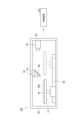
- FIG. 1 is a perspective view schematically showing the substrate processing system according to the first embodiment.
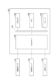
- FIG. 2 is a side view schematically showing an example of the coating and developing apparatus.
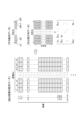
- FIG. 3 is a schematic diagram showing an example of an inspection unit.
- FIG. 4 is a block diagram showing an example of the functional configuration of the control device.
- FIG. 5 is a block diagram showing an example of the hardware configuration of the control device.
- FIG. 6 is a schematic diagram showing an example of the board inspection method.
- FIG. 7 is a flowchart showing an example of inspection processing in the preparation phase.
- FIG. 8 is a diagram schematically showing an example of an extracted image extracted from the intermediate layer.
- FIG. 9 is a diagram for explaining an example of the process of calculating the Mahalanobis distance.
- FIG. 1 is a perspective view schematically showing the substrate processing system according to the first embodiment.
- FIG. 2 is a side view schematically showing an example of the coating and developing apparatus.
- FIG. 3 is a schematic diagram showing an example
- FIG. 10 is a graph for conceptually explaining an example of the Mahalanobis distance.
- FIG. 11 is a flowchart showing an example of inspection processing in the production phase.
- FIG. 12 is a schematic diagram showing an example of a substrate inspection method according to the second embodiment.
- FIG. 13 is a schematic diagram showing an example of a substrate inspection method according to the second embodiment.
- FIG. 14 is a flow chart showing an example of a series of processes executed in the board inspection method.
- FIG. 15 is a flow chart showing an example of the inspection preparation process.
- FIG. 16 is a flow chart showing an example of inspection processing for a work.
- FIG. A substrate processing system 1 shown in FIG. 1 is a system for forming a photosensitive film on a work W, exposing the photosensitive film, and developing the photosensitive film.
- the workpiece W to be processed is, for example, a substrate, or a substrate on which a film, a circuit, or the like is formed by performing a predetermined process.
- a substrate included in the work W is, for example, a wafer containing silicon.
- the workpiece W (substrate) may be circular.
- the workpiece W to be processed may be a glass substrate, a mask substrate, an FPD (Flat Panel Display), or the like, or may be an intermediate obtained by subjecting these substrates or the like to predetermined processing.
- a photosensitive film is, for example, a resist film.
- a substrate processing system 1 includes a coating and developing device 2 and an exposure device 3 .
- the exposure device 3 performs exposure processing of a resist film (photosensitive film) formed on a work W (substrate). Specifically, the exposure device 3 irradiates an exposure target portion of the resist film with an energy beam by a method such as liquid immersion exposure.
- the coating and developing device 2 performs processing for forming a resist film on the surface of the work W before exposure processing by the exposure device 3, and performs development processing for the resist film after the exposure processing.
- the coating and developing apparatus 2 includes a carrier block 4, a processing block 5, an interface block 6, and a control device 100.
- FIG. 1 the coating and developing apparatus 2 includes a carrier block 4, a processing block 5, an interface block 6, and a control device 100.
- the carrier block 4 introduces the work W into the coating and developing device 2 and takes out the work W from the coating and developing device 2 .
- the carrier block 4 can support a plurality of carriers C (storage units) for works W, and incorporates a transfer device A1 including a transfer arm.
- the carrier C accommodates a plurality of circular works W, for example.
- the transport device A1 takes out the work W from the carrier C, transfers it to the processing block 5, receives the work W from the processing block 5, and returns it to the carrier C.
- the processing block 5 has a plurality of processing modules 11,12,13,14.
- the processing module 11 incorporates a liquid processing unit U1, a thermal processing unit U2, an inspection unit U3, and a transport device A3 that transports the work W to these units.
- the processing module 11 forms a lower layer film on the surface of the workpiece W using the liquid processing unit U1 and the heat processing unit U2.
- the liquid processing unit U1 of the processing module 11 coats the work W with a processing liquid for forming the lower layer film.
- the heat treatment unit U2 of the treatment module 11 performs various heat treatments associated with the formation of the lower layer film.
- the inspection unit U3 performs a process for inspecting the state of the surface of the workpiece W before the lower layer film is formed, after the lower layer film is formed, or before the treatment liquid for forming the lower layer film is applied and the heat treatment is performed. conduct.
- the processing module 12 incorporates a liquid processing unit U1, a thermal processing unit U2, an inspection unit U3, and a transport device A3 that transports the work W to these units.
- the processing module 12 forms a resist film on the lower layer film by the liquid processing unit U1 and the thermal processing unit U2.
- the liquid processing unit U1 of the processing module 12 applies a processing liquid (resist) for forming a resist film onto the underlying film.
- the heat treatment unit U2 of the processing module 12 performs various heat treatments associated with the formation of the resist film.
- the inspection unit U3 performs processing for inspecting the state of the surface of the work W before forming the resist film, after forming the resist film, or before applying the resist and performing heat treatment.
- the processing module 13 incorporates a liquid processing unit U1, a thermal processing unit U2, an inspection unit U3, and a transport device A3 that transports the work W to these units.
- the processing module 13 forms an upper layer film on the resist film using the liquid processing unit U1 and the thermal processing unit U2.
- the liquid processing unit U1 of the processing module 13 applies a processing liquid for forming an upper layer film onto the resist film.
- the heat treatment unit U2 of the treatment module 13 performs various heat treatments associated with the formation of the upper layer film.
- the inspection unit U3 performs processing for inspecting the state of the surface of the workpiece W before the upper layer film is formed, after the upper layer film is formed, or before the treatment liquid for upper layer film formation is applied and the heat treatment is performed. .
- the processing module 14 incorporates a liquid processing unit U1, a thermal processing unit U2, an inspection unit U3, and a transport device A3 that transports the work W to these units.
- the processing module 14 develops the resist film after exposure using the liquid processing unit U1 and the thermal processing unit U2.
- the liquid processing unit U1 of the processing module 14 develops the resist film by, for example, supplying the developing liquid onto the surface of the workpiece W that has been exposed and then washing it away with the rinsing liquid.
- the thermal processing unit U2 of the processing module 14 performs various types of thermal processing associated with development processing. Specific examples of heat treatment include heat treatment before development (PEB: Post Exposure Bake) and heat treatment after development (PB: Post Bake).
- the inspection unit U3 is for inspecting the state of the surface of the work W before development processing and PEB are performed, after development processing and PB are performed, or before PB is performed after the developer is supplied. process.
- a shelf unit U10 is provided on the side of the carrier block 4 in the processing block 5.
- the shelf unit U10 is partitioned into a plurality of vertically aligned cells.
- a transport device A7 including an elevating arm is provided in the vicinity of the shelf unit U10. The transport device A7 raises and lowers the work W between the cells of the shelf unit U10.
- a shelf unit U11 is provided on the interface block 6 side in the processing block 5.
- the shelf unit U11 is partitioned into a plurality of vertically aligned cells.
- the interface block 6 exchanges the workpiece W with the exposure apparatus 3.
- the interface block 6 incorporates a transfer device A8 including a transfer arm and is connected to the exposure device 3.
- FIG. The transport device A8 passes the work W placed on the shelf unit U11 to the exposure device 3, receives the work W from the exposure device 3, and returns it to the shelf unit U11.
- the control device 100 controls each device included in the coating and developing apparatus 2 so as to execute coating and developing processing (substrate processing), for example, in the following procedure.
- the control device 100 controls the transport device A1 to transport the work W in the carrier C to the shelf unit U10, and controls the transport device A7 to arrange the work W in the cell for the processing module 11.
- the control device 100 controls the transfer device A3 so as to transfer the work W on the shelf unit U10 to the liquid processing unit U1 in the processing module 11.
- the control device 100 controls the liquid processing unit U1 so as to form a film of the processing liquid for forming the lower layer film on the surface of the work W.
- the control device 100 controls the thermal processing unit U2 so as to heat the workpiece W on which the film of the treatment liquid for forming the lower layer film is formed, thereby forming the lower layer film.
- the control device 100 controls the transfer device A3 to return the work W on which the lower layer film is formed to the shelf unit U10, and controls the transfer device A7 to arrange this work W in the cell for the processing module 12.
- the control device 100 may control the inspection unit U3 so as to inspect the surface of the work W at any timing during the processing in the processing module 11 .
- the control device 100 controls the transfer device A3 so as to transfer the work W on the shelf unit U10 to the liquid processing unit U1 in the processing module 12.
- the control device 100 controls the liquid processing unit U1 so as to form a film of processing liquid for forming a resist film on the surface of the work W.
- FIG. The control device 100 controls the thermal processing unit U2 so as to heat the workpiece W on which the film of the treatment liquid for forming the resist film is formed to form the resist film.
- the control device 100 controls the transport device A3 to return the work W to the shelf unit U10, and controls the transport device A7 to place the work W in the cell for the processing module 13.
- the control device 100 may control the inspection unit U3 so as to inspect the surface of the work W at any timing of the processing within the processing module 12 .
- control device 100 controls the transport device A3 so as to transport the work W on the shelf unit U10 to the liquid processing unit U1 in the processing module 13. Further, the control device 100 controls the liquid processing unit U1 so as to form a film of the processing liquid for forming the upper layer film on the resist film of the workpiece W.
- FIG. The control device 100 controls the thermal processing unit U2 so as to heat the workpiece W on which the film of the treatment liquid for forming the upper layer film is formed, thereby forming the upper layer film.
- the control device 100 controls the transport device A3 to transport the work W to the shelf unit U11.
- the control device 100 may control the inspection unit U3 so as to inspect the surface of the work W at any timing during the processing in the processing module 13 .
- control device 100 controls the transport device A8 so as to send out the workpiece W on the shelf unit U11 to the exposure device 3. After that, the control device 100 controls the transport device A8 so that the work W subjected to the exposure processing is received from the exposure device 3 and arranged in the cell for the processing module 14 in the shelf unit U11.
- control device 100 controls the transport device A3 to transport the work W on the shelf unit U11 to each unit in the processing module 14, and controls the liquid processing unit U1 to develop the resist film of the work W. and heat treatment unit U2.
- the control device 100 controls the transport device A3 to return the work W to the shelf unit U10, and controls the transport devices A7 and A1 to return the work W to the carrier C.
- the control device 100 may control the inspection unit U3 so as to inspect the surface of the workpiece W at any timing during the processing in the processing module 14 .
- the coating and developing process for one work W is completed.
- the control device 100 controls each device of the coating and developing device 2 so as to perform the coating and developing process for each of the subsequent works W in the same manner as described above.
- the specific configuration of the substrate processing apparatus is not limited to the configuration of the coating and developing apparatus 2 illustrated above.
- the substrate processing apparatus may be of any type as long as it has a unit for inspecting the surface of the workpiece W to be subjected to predetermined processing, and a control device for controlling this unit.
- the inspection unit U3 has a function of capturing an image of the surface of the workpiece W (hereinafter referred to as "surface Wa") and acquiring image data.
- the inspection unit U3 may acquire image data of the entire surface Wa of the workpiece W by imaging the entire surface Wa.
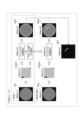
- the inspection unit U3 includes, for example, a housing 30, a holding section 31, a linear driving section 32, an imaging section 33, and a light projecting/reflecting section .
- the holding part 31 horizontally holds the work W with the surface Wa facing upward.
- the linear driving section 32 includes a power source such as an electric motor, and moves the holding section 31 along a horizontal linear path.
- the imaging unit 33 has a camera 35 such as a CCD camera.
- the camera 35 is provided near one end in the inspection unit U3 in the moving direction of the holding part 31, and faces the other end in the moving direction.
- the light projecting/reflecting unit 34 projects light onto an imaging range and guides reflected light from the imaging range to the camera 35 .
- the light projecting/reflecting unit 34 has a half mirror 36 and a light source 37 .
- the half mirror 36 is provided at a position higher than the holding portion 31 and in the intermediate portion of the movement range of the linear driving portion 32 and reflects light from below to the camera 35 .
- the light source 37 is provided above the half mirror 36 and emits illumination light downward through the half mirror 36 .
- the inspection unit U3 operates as follows to acquire image data of the surface Wa of the work W.
- the linear driving section 32 moves the holding section 31 .
- the work W passes under the half mirror 36 .
- reflected light from each part of the surface Wa of the work W is sequentially sent to the camera 35 .
- the camera 35 forms an image of reflected light from each part of the surface Wa of the work W, and acquires image data of the surface Wa of the work W (the entire surface Wa).
- a captured image obtained by capturing an image of the surface Wa of the work W changes depending on the state of the surface Wa of the work W.
- FIG. That is, acquiring a captured image (captured image data) of the surface Wa of the work W corresponds to acquiring information indicating the state of the surface Wa of the work W.
- the captured image data acquired by the camera 35 is sent to the control device 100 .
- the state of the surface Wa of the workpiece W can be inspected based on the captured image data of the surface Wa. For example, the presence or absence of defects on the surface Wa of the work W can be inspected.
- image data in which pixel values are determined for each pixel may be simply referred to as an "image.”
- control device 100 has a processing control section 102 and an inspection control section 110 as functional components (hereinafter referred to as "functional modules").
- the processing executed by the processing control unit 102 and the examination control unit 110 corresponds to the processing executed by the control device 100 .
- the processing control section 102 controls the liquid processing unit U1 and the heat processing unit U2 so that the work W is subjected to the liquid processing and heat processing in the coating and developing processing described above.
- the inspection control unit 110 inspects the workpiece W based on the image data obtained from the inspection unit U3 at any stage when the coating and developing process is executed.
- the inspection of the work W includes determining the presence or absence of an abnormality (defect) on the surface Wa of the work W.
- FIG. Defects on the surface Wa include, for example, scratches, adherence of foreign matter, uneven application of the treatment liquid, non-application of the treatment liquid, and the like.
- the inspection control unit 110 prepares reference data to be used in the inspection from the reference work W (reference substrate) before performing the inspection.
- the inspection control unit 110 inspects a workpiece W to be inspected (a substrate to be inspected) based on the reference data.
- the work W for reference and the work W to be inspected are works (substrates) of the same type.
- the reference work W and the work W to be inspected are subjected to the coating and developing process under the same processing conditions, and at the same timing in the coating and developing process (for example, after coating the resist and before the heat treatment), the preparation and the preparation of the reference data are performed. An inspection of the workpiece W is performed.
- the inspection control unit 110 includes, as functional modules, a first input image acquisition unit 112, a first intermediate information acquisition unit 114, a first feature image generation unit 116, a reference image storage unit 118, a model storage unit 132, It has a second input image acquisition unit 122 , a second intermediate information acquisition unit 124 , a second feature image generation unit 126 , an abnormality determination unit 136 , and a determination result output unit 138 .
- the processing executed by each functional module of the inspection control unit 110 corresponds to the processing executed by the inspection control unit 110 (control device 100).
- the first input image acquisition unit 112 acquires a reference input image based on an image of the workpiece W for reference.
- the first intermediate information acquisition unit 114 inputs a reference input image to a neural network (hereinafter referred to as an “image recognition model M”) that has been constructed in advance so as to output the recognition result of the input image
- the image Reference intermediate information generated in the intermediate layer of the recognition model M is acquired.
- a first feature image generation unit 116 generates a reference feature image representing features of the reference input image based on the intermediate reference information.
- the reference image holding unit 118 holds (stores) the reference feature image generated by the first feature image generation unit 116 .
- the reference feature image generated by the first feature image generation unit 116 is the reference data used in the inspection of the workpiece W to be inspected.
- the model holding unit 132 holds the image recognition model M described above.
- the second input image acquisition unit 122 acquires an inspection input image based on an image of the surface Wa of the workpiece W to be inspected.
- the second intermediate information acquisition unit 124 acquires inspection intermediate information generated in an intermediate layer of the image recognition model M when an inspection input image is input to the image recognition model M.
- the second feature image generation unit 126 generates an inspection feature image representing features of the inspection input image based on the intermediate inspection information.
- the abnormality determination unit 136 determines whether there is an abnormality on the surface Wa of the workpiece W to be inspected based on the result of comparing the reference feature image and the inspection feature image.
- the determination result output unit 138 outputs the determination result by the abnormality determination unit 136 .
- the determination result output unit 138 may output an abnormality signal indicating that the work W to be inspected is abnormal when the abnormality determination unit 136 determines that the surface Wa of the work W has an abnormality.
- the determination result output unit 138 may output the abnormality signal to the processing control unit 102, may output it to a host controller, or may output it to an output device such as a monitor for informing an operator or the like of information. .
- the control device 100 is composed of one or more computers.
- the control device 100 has, for example, a circuit 150 shown in FIG. Circuitry 150 includes one or more processors 152 , memory 154 , storage 156 and input/output ports 158 .
- the storage 156 has a computer-readable storage medium such as a hard disk.
- the storage medium stores a program (board inspection program) for causing the controller 100 to execute a board inspection method, which will be described later.
- the storage medium may be a removable medium such as a non-volatile semiconductor memory, a magnetic disk and an optical disk.
- the memory 154 temporarily stores the program loaded from the storage medium of the storage 156 and the calculation result by the processor 152 .
- the processor 152 cooperates with the memory 154 to execute the above programs, thereby configuring each of the above functional modules.
- the input/output port 158 inputs/outputs electric signals to/from the liquid processing unit U1, the thermal processing unit U2, the inspection unit U3, and the like according to instructions from the processor 152.
- the hardware configuration of the control device 100 is not necessarily limited to configuring each functional module by a program.
- each functional module of the control device 100 may be composed of a dedicated logic circuit or an ASIC (Application Specific Integrated Circuit) integrated with this.
- ASIC Application Specific Integrated Circuit
- the control device 100 executes processing in the preparation phase and processing in the production phase.
- the preparation phase the control device 100 performs coating and development processing on the reference work W, and then prepares for inspection of the work W in the production phase.
- the production phase the control device 100 sequentially performs the coating and developing process on a plurality of works W, and then inspects each work W to be subjected to the coating and developing process.
- the work W to be inspected in the production phase corresponds to the above-described work W to be inspected.
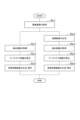
- FIG. 7 is a flow chart showing a series of processes in the preparation phase shown in FIG. 7.
- the reference work W determined to be processed normally is conveyed to the inspection unit U3. to start with.
- the control device 100 first executes step Sa-1.
- step Sa-1 for example, the first input image acquisition unit 112 of the inspection control unit 110 images the surface Wa of the reference work W by the inspection unit U3, thereby obtaining an image of the surface Wa of the reference work W.
- a captured image PIr is obtained.
- the captured image PIr may be a color image.
- the captured image PIr may include the entire surface Wa, and the number of pixels in the horizontal direction and the number of pixels in the vertical direction may be the same in the captured image PIr.
- the control device 100 executes step Sa-2.
- step Sa-2 for example, the first input image acquisition unit 112 generates an enhanced image EIr by performing a contrast enhancement process on the captured image PIr obtained at step Sa-1.
- contrast enhancement processing for example, the difference between a bright portion and a dark portion on the image (difference in brightness) is enhanced.
- the first input image acquisition unit 112 may perform contrast enhancement processing using various techniques.
- the first input image acquiring unit 112 may perform contrast enhancement processing on the captured image PIr by deforming (adjusting) the tone curve.
- the first input image acquisition unit 112 may perform contrast enhancement processing by applying a known spatial filter to the captured image PIr.
- step Sa-3 for example, when the first intermediate information acquisition unit 114 inputs the enhanced image EIr (reference input image) obtained in step Sa-2 to the image recognition model M, the image recognition model M Get reference intermediate information generated in the intermediate layer. For example, in the intermediate layer of the image recognition model M, the first intermediate information acquisition unit 114 generates a plurality of extracted images CIr (a plurality of reference Extracted image group CIGr including extracted images) is obtained as reference intermediate information.
- CIr a plurality of reference Extracted image group CIGr including extracted images
- the image recognition model M is a model constructed in advance by machine learning so that when an image is input, the results (recognition results) of classifying the content contained in the image into categories are output.
- the image recognition model M may be a multilayer neural network constructed by deep learning.
- the image recognition model M may be a CNN (Convolutional Neural Network).
- the image recognition model M does not have to be a model constructed to classify the workpiece W in the image into categories according to predetermined conditions.
- the image recognition model M may be a model for recognizing types of objects (for example, animals and fruits), a model for recognizing human faces, or a model for recognizing characters.
- a CNN may consist of an input layer, multiple convolutional layers, a pooling layer, a fully connected layer, and an output layer.
- a plurality of filters are used in the convolution layer (intermediate layer) included in the image recognition model M, and convolution is performed on the input image to that layer.
- a filter is also called a kernel, and each file is grid-like numerical data representing a specific shape (feature). The filter size is smaller than the input image size.
- a plurality of filters are set so as to obtain mutually different shapes (features) in the convolution layer.
- the product between a partial image (window) of the same size as the filter in the input image and the filter is calculated pixel by pixel, and the product of all pixels is calculated.
- a conversion process is performed to calculate the sum of the calculation results of . Then, the transformation process is repeated over the entire input image while moving the position of the partial image by a predetermined number of pixels.
- the multiple extracted images CIr acquired by the first intermediate information acquisition unit 114 are multiple images obtained by performing convolution using N filters in any one of the multiple convolution layers. . N is a natural number of 2 or more.
- the first intermediate information acquiring unit 114 inputs the enhanced image EIr obtained in step Sa-2 to the image recognition model M held by the model holding unit 132, and then selects a plurality of intermediate information from the intermediate calculation results of the image recognition model M. may be acquired.
- an image obtained by capturing the surface Wa of the work W is input to the image recognition model M, and convolution is performed using N filters in any one of a plurality of convolution layers.
- the group of extracted images CIG that are obtained are shown schematically.
- the extracted image group CIG includes a plurality of extracted images CI.
- a plurality of extracted images CI obtained when the input image to the image recognition model M is the enhanced image EIr corresponds to the plurality of extracted images CIr.
- the multiple extracted images CI include extracted images CI1, CI2, . . . , CIN.
- N is, for example, 230-270. In the following, a case where one extracted image CI has 255 vertical pixels and 255 horizontal pixels will be exemplified.
- the plurality of extracted images CI may be grayscale images.
- the image recognition model M may perform calculation after converting the image into a grayscale image.
- extracted images other than the extracted images CI1, CI2, CI3, CIj, and CIN are simplified by simple circles, but these extracted images also have pixel values.
- step Sa-0 the control device 100 determines whether or not the series of processes of steps Sa-1 to Sa-3 has been executed for a predetermined number of reference works W.
- the predetermined number of sheets is set, for example, to a number that can eliminate individual differences in the workpieces W for reference. If it is determined that the series of processes has not been executed for the predetermined number of reference works W (step Sa-0: NO), the process executed by the control device 100 returns to step Sa-1. Then, the control device 100 executes a series of processes of steps Sa-1 to Sa-3 for the reference works W of different individuals.
- step Sa-0 when it is determined that a series of processes have been executed for the predetermined number of reference works W (step Sa-0: YES), the process executed by the control device 100 proceeds to step Sa-4. move on.
- the first feature image generating unit 116 performs an operation for generating a reference feature image DIr based on the plurality of extracted images CIr obtained at step Sa-3.
- the first feature image generation unit 116 calculates a Mahalanobis distance (reference Mahalanobis distance) based on the data distribution of the plurality of extracted images CIr for the array data of pixel values (brightness values) for each pixel included in the plurality of extracted images CIr. calculate.
- the first feature image generation unit 116 may calculate the Mahalanobis distance for each of a plurality of reference works W (each reference work W).
- FIG. 9 the vertical coordinate on the image is represented by "i"
- the horizontal coordinate is represented by "j”.
- a pixel (i, j) indicates a pixel located in the i-th row and the j-th column, and i and j are natural numbers from 1 to N, respectively.
- array data of pixel values is created for extracted images CIr1, CIr2, .
- the pixel values of all the pixels included in the extracted image CIr1 can be represented by one column of array data arranged vertically.
- the pixel values of all the pixels in the extracted image CIr1 obtained from each of a plurality of reference works W are shown as vertically arranged array data as a variable x1.
- the pixel values of all the pixels in the extracted image CIr2 obtained from each of a plurality of reference works W are indicated by vertically aligned array data as a variable x2.
- the pixel values of all the pixels in the extracted images CIr3 to CIrN-1 obtained from each of the plurality of reference works W are indicated by vertically arranged array data as variables x3 to xN-1, respectively. .
- N array data indicated by variables x1 to xN are arranged in order in the horizontal direction.
- N array data indicated by variables x1 to xN are N-dimensional data because they contain N variables.
- the order in which the coordinates are arranged is the same for each array data arranged vertically. Therefore, in a plurality of array data arranged in the horizontal direction, the pixel values of the pixels (i, j) at the same coordinates in the variables x1 to xN are arranged in the horizontal direction. For example, regarding the first reference work W, the pixel value of the variable x1 at the pixel (1,1), the pixel value of the variable x2 at the pixel (1,1), and the pixel value of the pixel (1,1) Pixel values of variables x3 to xN are arranged in the first row of the array data in FIG.
- xn an arbitrary variable out of variables x1 to xN is written as "xn", and n means any one natural number from 1 to N.
- a pixel value of a pixel (i, j) at a specific coordinate in the variable xn is expressed as "xn[i, j]”.
- x1[i,j], x2[i,j], . . . , and xN[i,j] are arranged horizontally in this order.
- the first characteristic image generation unit 116 performs the process of arranging the values (pixel values) included in each of the plurality of extracted images CIr in the vertical direction with respect to the plurality of works W for reference.
- the first feature image generation unit 116 calculates average array data indicating the average for each variable and a covariance matrix.
- FIG. 10 shows a graph for explaining the concept of Mahalanobis distance.
- the concept of Mahalanobis distance obtained from one reference work W and calculated from two-dimensional array data of only variables x1 and x2 will be described.
- the horizontal axis is the variable x1 and the vertical axis is the variable x2.
- values (x1[i,j], x2[i,j]) of combinations of variables x1 and x2 are plotted for each pixel (coordinates).
- Mean(x1) which is the average value of the variable x1
- the distances from the value of the combination with Mean(x2), which is the average value substantially match.
- m1, m2, n1, and n2 are any one natural number from 1 to N;
- the value of the combination of pixel values indicated by [m2, n2] deviates from the distribution of the values of the combination of variables x1 and x2 compared to the value of the combination of pixel values indicated by [m1, n1].
- the Mahalanobis distance can represent the degree of deviation (abnormality) from the data distribution of the variables x1 and x2.
- the first feature image generation unit 116 calculates the average array data (average) shown in FIG. 9 by calculating the average ⁇ n of the pixel values for each variable xn (for each of the variables x1 to xN).
- the average .mu.n is calculated from one column of array data included in the variable xn, and is the arithmetic mean of pixel values of all pixels of all reference works W in that column.
- the first feature image generation unit 116 calculates the variance ⁇ n for each variable xn (for each of the variables x1 to xN) from the vertically arranged array data of the pixel values.
- the first feature image generator 116 calculates a correlation coefficient Srs (covariance) for each combination of two variables out of the variables x1 to xN. Each of r and s in the correlation coefficient Srs satisfies r ⁇ s and is a natural number from 1 to N. A covariance matrix is obtained by calculating the variance ⁇ n and the correlation coefficient Srs
- the first feature image generation unit 116 uses the pixel values for each pixel (i, j) in the variables x1 to xN for one reference work W in the horizontal direction.
- the Mahalanobis distance is calculated for the arranged sequence data.
- the first feature image generation unit 116 calculates the Mahalanobis distance from the array data of the pixel values of each pixel for all the pixels related to one reference work W.
- FIG. In this case, one Mahalanobis distance is calculated for one pixel in all pixels.
- the Mahalanobis distance at pixel (i, j) is denoted as "distance MD(i, j)"
- a set of distances MD(i, J) at all pixels is defined as "MD data”.
- the first feature image generating unit 116 similarly calculates the Mahalanobis distance from the pixel value array data of each pixel for all pixels of other (second and subsequent) reference works W. As a result, a plurality of pieces of MD data are generated for a plurality of works W for reference.
- reference works W other than the work W It also includes calculating using means and covariance matrices that are also calculated using data obtained from .
- step Sa-5 for example, the first characteristic image generation unit 116 generates a reference characteristic image DIr from the plurality of MD data obtained at step Sa-4. For each pixel (i, j), the first feature image generation unit 116 calculates the value ( pixel value). The first feature image generation unit 116 may calculate the maximum value or average value of multiple distances MD(i, j) for each pixel (i, j) as the pixel value in the reference feature image DIr.
- the reference image storage unit 118 After calculating the pixel values of the reference feature image DIr for all pixels (i, j), the reference image storage unit 118 stores the reference feature image DIr. As described above, a series of processes in the preparation phase is completed, and a reference feature image DIr, which is reference data used for inspection in the production phase, is generated. In the series of processes exemplified above, one reference feature image DIr is obtained from a plurality of enhanced images EIr obtained for at least two reference works W. FIG. Note that one reference feature image DIr may be obtained from the enhanced image EIr for one reference work W instead of two or more reference works W. FIG. Instead of calculating the mean and covariance matrix from the sequence data obtained from all reference works W, the mean and covariance matrices are calculated for each reference work W, and the Mahalanobis distance is calculated. good too.
- each functional module of the inspection control unit 110 is: Do the following:
- the first input image acquisition unit 112 acquires an enhanced image EIr1 based on an image of the surface Wa of the reference work Wr1, and an image of the surface Wa of the reference work Wr2 (reference second substrate).
- the first intermediate information acquisition unit 114 acquires the first intermediate information generated in the intermediate layer when the enhanced image EIr1 is input to the image recognition model M, and the intermediate information when the enhanced image EIr2 is input to the image recognition model M.
- second intermediate information second reference intermediate information
- the first feature image generation unit 116 generates a reference feature image DIr based on the first intermediate information and the second intermediate information.
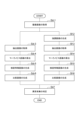
- FIG. 11 is a flow chart showing a series of processes in the production phase shown in FIG. The series of processes shown in FIG. 11 is started after the pre-inspection process of the coating and developing process has been performed, and the work W to be inspected, whose inspection result is unknown, is transported to the inspection unit U3. do.
- Step Sb-1 is performed under the same conditions as the processing of step Sa-1 in the preparation phase.
- the second input image acquisition unit 122 of the inspection control unit 110 captures an image of the surface Wa of the workpiece W to be inspected by the inspection unit U3, thereby obtaining an image of the surface Wa of the workpiece W to be inspected.
- a captured image PIs is acquired.
- Step Sb-2 is performed under the same conditions as the processing of step Sa-2 in the preparation phase.
- the second input image acquisition unit 122 generates an enhanced image EIs by performing a contrast enhancement process on the captured image PIs obtained in step Sb-1.
- Step Sb-3 is performed under the same conditions as the processing of step Sa-3 in the preparation phase.
- the image recognition model M Acquire an inspection intermediate image generated in the intermediate layer.
- the second intermediate information acquisition unit 124 generates a plurality of extracted images CIs (a plurality of Extracted image group CIGs including inspection extracted images) is acquired as intermediate inspection information.
- the multiple filters used in generating multiple extracted images CIs are the same as the multiple filters used in generating multiple extracted images CIr in the preparation phase. If there is an arcuate flaw on the surface Wa of the workpiece W to be inspected, the filter reacts to the arcuate flaw in the intermediate layer of the image recognition model M, as shown in the "extracted image CIj" shown in FIG. An extracted image CI (feature map) can be generated.
- Step Sb-4 is performed in a manner similar to step Sa-4 in the preparation phase.
- the second characteristic image generation unit 126 performs an operation for generating an inspection characteristic image DIs based on the plurality of extracted images CIs acquired at step Sb-3.
- the second feature image generation unit 126 generates array data of pixel values (brightness values) for each pixel (i, j) included in a plurality of extracted images CIs, and extracts any extracted image group CIGr obtained in the preparation phase.
- the Mahalanobis distance is calculated based on the data distribution of the plurality of extracted images CIr.
- the second feature image generation unit 126 performs processing for arranging pixel values included in each of the variables x1 to XN corresponding to the N extracted images CIs in a vertical array in the same manner as in step Sa-4 in the preparation phase. do.
- the second feature image generation unit 126 uses the average and the covariance matrix obtained from the plurality of extracted images CIr in step Sa-4 for each pixel (i, j) included in the N extracted images CIs.
- the Mahalanobis distance is calculated for array data arranged in the horizontal direction of the pixel values of .
- the average and covariance matrix used when generating the reference data are used instead of the average and covariance matrix obtained from the data for which the distance is calculated. Calculation is also included.
- step Sb-5 for example, the second feature image generation unit 126 generates an inspection feature image DIs based on the Mahalanobis distance calculation result at step Sb-4.
- the second feature image generator 126 may set the Mahalanobis distance calculated in step Sb-4 to the pixel value of each pixel (i, j).
- step Sb-6 for example, the abnormality determination unit 136 compares the inspection feature image DIs generated in step Sb-5 with the reference feature image DIr held by the reference image holding unit 118, thereby obtaining a comparison image DiI. to generate The abnormality determination unit 136 calculates the difference between the pixel value of the inspection feature image DIs and the pixel value of the reference feature image DIr for each pixel (i, j), thereby determining the pixel value of the pixel of the comparison image DiI. can be calculated.
- step Sb-7 for example, the abnormality determination unit 136 determines the workpiece W to be inspected based on the result of comparing the inspection feature image DIs and the reference feature image DIr (comparison image DiI generated in step Sb-6). The presence or absence of abnormality on the surface Wa is determined.
- the abnormality determination unit 136 executes processing for extracting pixels having a pixel value equal to or greater than a predetermined value in the inspection feature image DIs.
- the predetermined value is set to such an extent that when a defect occurs on the surface Wa of the workpiece W, the pixel value at the defective portion can be extracted.
- the abnormality determination unit 136 may determine that there is an abnormality on the surface Wa of the workpiece W to be inspected when an area (or pixel) having a pixel value equal to or greater than a predetermined value is detected in the comparison image DiI.
- the abnormality determination unit 136 may determine that there is no abnormality on the surface Wa of the workpiece W to be inspected when no region (or pixel) having a pixel value equal to or greater than a predetermined value is detected in the comparison image DiI. .
- step Sb-8 for example, the determination result output unit 138 outputs information indicating the determination result in step Sb-7 to the processing control unit 102 or the host controller.
- the determination result output unit 138 outputs information indicating the determination result in step Sb-7 to the processing control unit 102 or the host controller.
- the board inspection method obtains a reference input image based on an image of the surface Wa of the workpiece W for reference, and outputs the recognition result of the input image. obtaining reference intermediate information generated in an intermediate layer of the image recognition model M when a reference input image is input to a pre-constructed neural network (image recognition model M); generating a reference feature image DIr indicative of features of the input image.
- the above substrate inspection method acquires an inspection input image based on an image of the surface Wa of the workpiece W to be inspected, and when the inspection input image is input to the image recognition model M, an intermediate layer of the image recognition model M and generating an inspection feature image DIs representing features of the inspection input image based on the intermediate inspection information.
- the board inspection method further includes determining whether or not there is an abnormality on the surface Wa of the workpiece W to be inspected based on the result of comparing the reference feature image DIr and the inspection feature image DIs.
- the reference feature image DIr generated from the information generated in the intermediate layer of the image recognition model M can represent the features of the entire surface Wa of the workpiece W for reference.
- the inspection feature image DIs generated from the information generated in the intermediate layer of the image recognition model M can represent the features of the entire surface Wa of the workpiece W to be inspected.
- the reference intermediate information is a plurality of reference extracted images ( It may be a plurality of extracted images CIr).
- Generating the reference feature image DIr may include generating the reference feature image DIr based on the plurality of extracted images CIr.
- the intermediate inspection information may be a plurality of inspection extracted images (a plurality of extracted images CIs) generated in the intermediate layer of the image recognition model M based on the inspection input image and the plurality of filters.
- Generating the inspection feature image DIs may include generating the inspection feature image DIs based on the plurality of extracted images CIs.
- various specific shapes are extracted by a plurality of filters in the intermediate layers of the image recognition model M. FIG. By extracting various specific shapes, when the surface Wa of the work W includes an abnormal portion, the abnormal portion can be extracted in response to the filter. Therefore, it is useful for highly accurate abnormality detection on the surface Wa of the work W.
- the generation of the reference feature image DIr is based on the data distribution of the plurality of extracted images CIr for the pixel value array data for each pixel (i, j) included in the plurality of extracted images CIr.
- Generating the inspection feature image DIs is performed by combining the average and covariance matrix used in calculating the reference Mahalanobis distance for array data of pixel values for each pixel (i, j) included in a plurality of extracted images CIs.
- the Mahalanobis distance can represent the degree of deviation (abnormality) from the data distribution. Therefore, if there is an abnormal portion on the surface Wa, the pixel value of a specific pixel will fluctuate in response to the filter in the image recognition model M. FIG. This can lead to large values of the Mahalanobis distance at a particular pixel. In the above configuration, since the feature images are compared with each other, areas where the Mahalanobis distance is large due to the features of the workpiece W itself are canceled out, and then areas where the Mahalanobis distance is large due to the abnormal part are detected. can be done. Therefore, it is more useful for highly accurate abnormality detection on the surface Wa of the work W. FIG.
- the reference input image may be an enhanced image EIr generated by performing a contrast enhancement process on the captured image PIr of the surface Wa of the workpiece W for reference. good.
- the inspection input image may be an enhanced image EIs generated by performing a contrast enhancement process on the captured image PIs of the surface Wa of the workpiece W to be inspected.
- the substrate processing method described above acquires a second reference input image based on an image of the surface Wa of another workpiece W for reference, and when the second reference input image is input to the image recognition model M, and obtaining second reference intermediate information generated in an intermediate layer of the image recognition model M.
- Generating the reference feature image DIr may include generating the reference feature image DIr based on the intermediate reference information and the second intermediate reference information.
- one reference feature image DIr is generated from a plurality of captured images of the surface Wa of the workpiece W for reference. Therefore, the reference feature image DIr can be generated after reducing the influence of the feature of one reference work W individual. Therefore, it is more useful for highly accurate abnormality detection on the surface Wa of the work W.
- the substrate processing system 1 according to the second embodiment will be described with reference to FIGS. 12 to 16.
- the coating and developing apparatus 2 may perform coating and developing processing (substrate processing) on a predetermined number of works W per lot.
- the coating and developing apparatus 2 sequentially performs the coating and developing process on a predetermined number of works W in the process for each lot (lot process).
- the predetermined number indicating the lot unit may be determined according to the number of works W that can be accommodated in the carrier C.
- FIG. The coating and developing apparatus 2 repeatedly executes the coating and developing process for each lot.
- the inspection control unit 110 generates reference feature images, which are reference data used for inspection, while the production phase is being executed.
- the inspection control unit 110 generates a reference characteristic image using the workpiece W (first substrate) that is first processed in the coating and developing process for each lot.
- the work W to be processed first is the work W for reference, although the presence or absence of an abnormality on the surface Wa is unknown.
- the inspection control unit 110 uses the reference feature image to perform an inspection using the workpiece W (second substrate) to be inspected for the workpiece W (second substrate) that is to be processed second and subsequent in the coating and developing process for each lot.
- the inspection control unit 110 executes two different inspection procedures and determines whether or not there is an abnormality on the surface Wa of the work W from the results obtained from these inspection procedures. .
- FIG. 12 shows a series of processes executed in one inspection procedure
- FIG. 13 shows a series of processes executed in another inspection procedure.
- a reference feature image is generated from the first workpiece W in any inspection procedure.
- FIG. 14 is a flowchart showing an example of a series of processes executed by the inspection control unit 110 for each lot.
- step 41 the control device 100 executes step 41 in a state in which the work W to be processed is conveyed to the inspection unit U3 after being subjected to the pre-inspection process of the coating and developing process. do.
- step S41 the inspection control unit 110 determines whether or not the work W to be processed that has been transported to the inspection unit U3 is the first work W in the lot-based processing.
- the inspection control unit 110 may count the number of works W inspected by the inspection unit U3 from the start of the production phase, thereby determining whether or not the work W is the first work W in each lot.
- step S41 if the workpiece W to be processed that has been transported to the inspection unit U3 is the first workpiece W (step S41: YES), the process executed by the control device 100 proceeds to step S50.
- step S50 for example, the inspection control unit 110 executes an inspection preparation process for inspecting the second and subsequent works W to be processed.
- FIG. 15 is a flow chart showing an example of the inspection preparation process in step S50.
- the inspection preparation process in step S50 includes a series of processes for the first sheet shown in FIG. 12 and a series of processes for the first sheet shown in FIG.
- step Sc-1 is performed in the same manner as step Sa-1 in the board inspection method according to the first embodiment.
- the first input image acquisition unit 112 of the inspection control unit 110 images the surface Wa of the first workpiece W by the inspection unit U3, thereby obtaining the surface Wa of the first workpiece W. to acquire a captured image PIr for .
- Step Sc-3 is performed in the same manner as step Sa-3 in the board inspection method according to the first embodiment.
- the image recognition model M Get reference intermediate information generated in the intermediate layer.
- the first intermediate information acquisition unit 114 generates a plurality of extracted images CIr1 (a plurality of reference Extracted image group CIGr1 including extracted images) is obtained as reference intermediate information.
- the number of extracted images CIr1 included in the extracted image group CIGr1 may be 30-60.
- Step Sc-4 is performed in the same manner as step Sa-4 in the board inspection method according to the first embodiment.
- the first characteristic image generation unit 116 generates array data of pixel values (brightness values) for each pixel (i, j) included in the plurality of extracted images CIr1.
- a Mahalanobis distance (reference Mahalanobis distance) is calculated based on the data distribution.
- Step Sc-5 is executed in the same manner as step Sa-5 or step Sb-5 in the board inspection method according to the first embodiment.
- the first feature image generation unit 116 generates a reference feature image DIr1 based on the Mahalanobis distance calculation result at step Sc-4.
- the first feature image generator 116 may set the Mahalanobis distance calculated in step Sc-4 to the pixel value of the pixel in the reference feature image DIr1 for each pixel (i, j).
- the reference image holding unit 118 stores the reference feature image DIr1.
- Step Se-2 is executed in the same manner as Step Sa-2 in the board inspection method according to the first embodiment.
- the first input image acquiring unit 112 generates an enhanced image EIr2 by performing a contrast enhancement process on the captured image PIr obtained at step Sc-1.
- Step Se-3 is executed in the same manner as step Sc-3.
- the image recognition model M Get reference intermediate information generated in the intermediate layer.
- the first intermediate information acquisition unit 114 generates a plurality of An extracted image group CIGr2 including the extracted image CIr2 (a plurality of second reference extracted images) is obtained as reference intermediate information.
- the number of extracted images CIr2 included in the extracted image group CIGr2 may be different from the number of extracted images CIr1 included in the extracted image group CIGr1 obtained in step Sc-3, and is between 180 and 220. good too. That is, between step Sc-3 and step Se-3, the number of filters for generating the extracted image group may differ.
- Step Se-4 is executed in the same manner as step Sc-4.
- the first feature image generation unit 116 generates array data of pixel values (brightness values) for each pixel (i, j) included in the plurality of extracted images CIr1.
- a Mahalanobis distance (reference Mahalanobis distance) is calculated based on the data distribution.
- Step Se-5 is executed in the same manner as step Sc-5.
- the first feature image generation unit 116 generates a reference feature image DIr2 (second reference feature image) based on the Mahalanobis distance calculation result at step Se-4.
- the first feature image generator 116 may set the Mahalanobis distance calculated in step Se-4 to the pixel value of the pixel in the reference feature image DIr2 for each pixel (i, j).
- the reference image holding unit 118 stores the reference feature image DIr2.
- step S50 the inspection preparation process of step S50 is completed, and the reference feature image DIr1 and the reference feature image DIr2, which are the reference data used in the inspection of the second and subsequent works W, are generated.
- step S60 the abnormality determination unit 136 determines whether there is an abnormality on the surface Wa of the first workpiece W based on at least one of the reference feature image DIr1 and the reference feature image DIr2 (for example, the reference feature image DIr2). judge.
- the abnormality determination unit 136 executes a process of extracting pixels having a pixel value equal to or greater than a predetermined value in the reference feature image DIr2. may be determined to have an abnormality (defect).
- the abnormality of the surface Wa of the first workpiece W may be detected although the sensitivity is low.
- step S41 if the workpiece W to be processed that has been transported to the inspection unit U3 is any of the workpieces W after the second one (step S41: NO), the processing executed by the control device 100 is the step Proceed to S70.
- step S70 for example, the inspection control unit 110 inspects the second and subsequent workpieces W to be processed.
- FIG. 16 is a flowchart showing an example of inspection processing in step S70.
- the inspection process in step S70 includes a series of processes for the second and subsequent sheets shown in FIG. 12 and a series of processes for the second and subsequent sheets shown in FIG.
- step Sd-1 is executed under the same conditions as step Sc-1.
- step Sd-1 for example, the second input image acquisition unit 122 of the inspection control unit 110 captures the surface Wa of the workpiece W to be inspected that is processed second and subsequent times using the inspection unit U3. A captured image PIs of the workpiece W is obtained.
- Step Sd-3 is executed under the same conditions as step Sc-3.
- the image recognition model M Get the inspection intermediate information generated in the intermediate layer.
- the second intermediate information acquisition unit 124 generates a plurality of extracted images CIs1 (a plurality of inspection Extracted image group CIGs1 including extracted images) is acquired as intermediate inspection information.
- the plurality of filters used in step Sd-3 and the plurality of filters used in step Sc-3 are the same.
- Step Sd-4 is performed in the same manner as step Sb-4 in the board inspection method according to the first embodiment.
- the second feature image generating unit 126 generates array data of pixel values (luminance values) for each pixel (i, j) included in the plurality of extracted images CIs1 obtained in step Sd-3.
- the Mahalanobis distance is calculated based on the data distribution of the plurality of extracted images CIr1 obtained in step Sc-3.
- Step Sd-5 is executed in the same manner as step Sc-5.
- the second feature image generating unit 126 generates an inspection feature image DIs1 based on the Mahalanobis distance calculation result at step Sd-4.
- the second characteristic image generator 126 may set the Mahalanobis distance calculated in step Sd-4 to the pixel value of the pixel in the inspection characteristic image DIs1 for each pixel (i, j).
- Step Sd-6 is executed in the same manner as step Sb-6 in the board inspection method according to the first embodiment.
- the abnormality determination unit 136 compares the inspection feature image DIs1 generated in step Sd-5 with the reference feature image DIr1 held by the reference image holding unit 118, thereby obtaining a comparison image DiI1. to generate The abnormality determination unit 136 calculates the difference between the pixel value of the inspection feature image DIs1 and the pixel value of the reference feature image DIr1 for each pixel (i, j), thereby determining the pixel value of the pixel of the comparison image DiI1. can be calculated.
- step Sf-2 In parallel with the series of processes including steps Sd-3 to Sd-6, or after execution of the series of processes, the control device 100 executes step Sf-2.
- Step Sf-2 is executed under the same conditions as step Se-2.
- the second input image acquisition unit 122 generates an enhanced image EIs2 by performing a contrast enhancement process on the captured image PIs obtained in step Sd-1.
- Step Sf-3 is executed under the same conditions as step Se-3.
- step Sf-3 for example, when the second intermediate information acquiring unit 124 inputs the enhanced image EIs2 (inspection input image) obtained in step Sf-2 to the image recognition model M, the intermediate information of the image recognition model M Get inspection intermediate information generated by the layer.
- the second intermediate information acquisition unit 124 generates a plurality of An extracted image group CIGs2 including the extracted images CIs2 (a plurality of second inspection extracted images) is obtained as intermediate inspection information.
- the filters used in step Se-3 are the same as the filters used in step Sf-3.
- Step Sf-4 is executed in the same manner as step Se-4.
- the second feature image generation unit 126 generates array data of pixel values (brightness values) for each pixel (i, j) included in the plurality of extracted images CIs2 obtained in step Sf-3.
- the Mahalanobis distance is calculated based on the data distribution of the plurality of extracted images CIs2.
- the average and covariance matrix used in calculating the Mahalanobis distance to generate the reference data are used, whereas in step Sf-4, the self (a plurality of extracted images CIs2) The mean and covariance matrices obtained from are utilized.
- Step Sf-5 is executed in the same manner as step Se-5.
- the second characteristic image generator 126 generates an inspection characteristic image DIs2 (second inspection characteristic image) based on the result of calculating the Mahalanobis distance in step Sf-4.
- the second characteristic image generator 126 may set the Mahalanobis distance calculated in step Sf-4 to the pixel value of the pixel in the inspection characteristic image DIs2 for each pixel (i, j).
- Step Sf-6 is executed in the same manner as step Sd-6.
- the abnormality determination unit 136 compares the inspection feature image DIs2 generated in step Sf-5 with the reference feature image DIr2 held by the reference image holding unit 118, thereby obtaining a comparison image DiI2. to generate The abnormality determination unit 136 calculates the difference between the pixel value of the inspection feature image DIs2 and the pixel value of the reference feature image DIr2 for each pixel (i, j), thereby determining the pixel value of the pixel of the comparison image DiI2. can be calculated.
- step S47 the abnormality determination unit 136 determines the processing target based on the result of comparing the reference feature image DIr1 and the inspection feature image DIs1 and the result of comparing the reference feature image DIr2 and the inspection feature image DIs2. The presence or absence of abnormality on the surface Wa of the work W is determined. The abnormality determination unit 136 determines whether there is an abnormality on the surface Wa of the workpiece W to be processed based on the comparison image DiI1 obtained in step Sd-6 and the comparison image DiI2 obtained in step Sf-6. .
- the abnormality determination unit 136 executes processing for extracting pixels having a pixel value equal to or greater than a predetermined value in each of the comparison image DiI1 and the comparison image DiI2. If an area (or pixel) having a pixel value equal to or greater than a predetermined value is detected in at least one of the comparative image DiI1 and the comparative image DiI2, the abnormality determination unit 136 determines that the surface Wa of the workpiece W to be inspected has an abnormality. can be determined.
- the abnormality determination unit 136 determines that there is no abnormality on the surface Wa of the workpiece W to be inspected. can be determined.
- step S48 for example, the determination result output unit 138 outputs information indicating the determination results in steps S47 and S60 to the processing control unit 102 or the host controller.
- a workpiece W determined to have an abnormality (defect) on the surface Wa may be excluded from the processing line after inspection by the inspection unit U3. If an abnormality is detected in the first work W in step S60, the inspection control unit 110 executes step S50 for the second work W, and obtains reference data from the captured image of the second work W, etc. may be generated.
- step S49 the control device 100 determines whether or not inspection of a predetermined number of workpieces W defining a lot unit has been completed. If it is determined in step S49 that the predetermined number of workpieces W have not been inspected (step S49: NO), the process executed by the control device 100 returns to step S41. In step S49, when it is determined that the inspection of the predetermined number of works W has been completed (step S49: YES), the substrate inspection for one lot ends. The control device 100 (inspection control unit 110) performs the same board inspection process for the next lot.
- the substrate inspection method executed by the substrate processing system 1 according to the second embodiment also has the same effects as the first embodiment, and is useful for accurately detecting an abnormality on the surface Wa of the workpiece W. be.
- the generation of the reference feature image DIr2 is performed by: It may include calculating a pixel value for each pixel of the reference feature image DIr2 based on the result of calculating the reference Mahalanobis distance based on the data distribution of the plurality of extracted images CIr2.
- Generating the inspection feature image DIs2 involves obtaining an inspection Mahalanobis distance for array data of pixel values for each pixel included in a plurality of inspection extracted images (a plurality of extracted images CIs2) based on the data distribution of the plurality of extracted images CIs2. It may include calculating a pixel value for each pixel of the inspection feature image DIs2 based on the calculated result.
- the inspection Mahalanobis distance is calculated using the average and covariance matrix when the reference Mahalanobis distance is calculated when creating the reference data, the abnormality between the reference work W and the work W to be inspected Even changes that are not desired to be determined can be detected.
- the inspection Mahalanobis distance is calculated from its own data distribution, and the difference from the workpiece W for reference is not reflected in the inspection Mahalanobis distance. Therefore, it is useful for adjusting the detection sensitivity according to the type of abnormality to be detected.
- the reference work W is the first work W to be coated and developed in lot processing in which a predetermined number of works W to be processed are sequentially subjected to a predetermined coating and developing process. It may be the first work W to which is applied.
- the work W to be inspected may be any work W after the second work which is subjected to the coating and developing process in any order after the second work in lot processing. In this case, reference data for inspection is generated for each lot. Therefore, variations in the workpiece W itself or in the coating and developing process among a plurality of lots hardly affect the abnormality determination. Therefore, it is useful for highly accurate abnormality detection on the surface Wa of the work W.
- the image recognition model in addition to generating the reference feature image DIr1 and the inspection feature image DIs1, when the reference input image is input to the image recognition model M, the image recognition model obtaining a plurality of second reference extracted images (plurality of extracted images CIr2) generated based on a reference input image and a plurality of second filters for extracting features different from each other in an intermediate layer of M; generating a second reference feature image (reference feature image DIr2) based on the extracted image CIr2.
- a plurality of second inspections are generated based on the inspection input image and the plurality of second filters in an intermediate layer of the image recognition model M.
- the board inspection method according to the second embodiment described above may further include determining whether there is an abnormality on the surface Wa of the first workpiece W based on the reference feature image.
- the surface Wa of the first work W for generating the reference data for inspection contains a clear abnormality, the work W can be eliminated, and another work W can be used as a reference. Can create data. Therefore, it is useful for highly accurate abnormality detection on the surface Wa of the work W.
- the present disclosure is not limited to the first and second embodiments described above. Some items described in the first embodiment may be applied to the second embodiment, and some items described in the second embodiment may be applied to the first embodiment.
- the series of processes described above can be changed as appropriate. In the above series of processes, the control device 100 (examination control unit 110) may execute one step and the next step in parallel, or may execute each step in an order different from the above example. .
- the control device 100 (inspection control unit 110) may omit any of the steps, or may perform processing different from the above example in any of the steps.
- the inspection control unit 110 may omit steps Sa-2 and Sb-2. In this case, the inspection control unit 110 inputs the captured image PIr to the image recognition model M in step Sa-3, and inputs the captured image PIs to the image recognition model M in step Sb-3.
- the inspection control unit 110 according to the first embodiment may generate the reference feature image DIr, which is the reference data, from one work W for reference.
- the inspection control unit 110 executes two different inspection procedures, only one of them may be executed.
- the inspection control unit 110 determines whether there is an abnormality on the surface Wa of the workpiece W to be inspected based on the comparison image DiI1 obtained by executing the inspection procedure shown in FIG. 12 without executing the inspection procedure shown in FIG. You can judge.
- the inspection control unit 110 determines whether there is an abnormality on the surface Wa of the workpiece W to be inspected based on the comparison image DiI2 obtained by executing the inspection procedure shown in FIG. 13 without executing the inspection procedure shown in FIG. You can judge.
- the series of processes applied to the first workpiece W may be executed in the preparation phase before the production phase starts. Then, in the production phase, a series of processes to be applied to the second and subsequent works W may be performed on the works W to be processed regardless of the lot unit.
- the image recognition model M may be stored in an external device of the control device 100 without the inspection control unit 110 holding the image recognition model M.
- the inspection control unit 110 may acquire the extracted image group CIG from the external device after transmitting the captured image or the enhanced image to the external device.
- a computer that constitutes the inspection control unit 110 may be provided in addition to the coating and developing apparatus 2 .
- the control device 100 and the examination control unit 110 may be communicably connected via a wire, wireless, or network.
- the control device 100 may acquire the captured image from the inspection unit U ⁇ b>3 and then transmit the captured image to the inspection control section 110 .
- the inspection control unit 110 may transmit information indicating the determination result of the presence/absence of abnormality to the control device 100 . At least part of the items described in the other examples may be applied to one of the various examples described above.
Landscapes
- Engineering & Computer Science (AREA)
- Physics & Mathematics (AREA)
- General Physics & Mathematics (AREA)
- Computer Vision & Pattern Recognition (AREA)
- Theoretical Computer Science (AREA)
- Quality & Reliability (AREA)
- Chemical & Material Sciences (AREA)
- Life Sciences & Earth Sciences (AREA)
- Health & Medical Sciences (AREA)
- Analytical Chemistry (AREA)
- Biochemistry (AREA)
- General Health & Medical Sciences (AREA)
- Immunology (AREA)
- Pathology (AREA)
- Signal Processing (AREA)
- Image Analysis (AREA)
- Investigating Materials By The Use Of Optical Means Adapted For Particular Applications (AREA)
- Image Processing (AREA)
Priority Applications (5)
| Application Number | Priority Date | Filing Date | Title |
|---|---|---|---|
| CN202280080156.8A CN118355266A (zh) | 2021-12-10 | 2022-11-28 | 基片检查方法、基片检查程序和基片检查装置 |
| KR1020247022150A KR20240117592A (ko) | 2021-12-10 | 2022-11-28 | 기판 검사 방법, 기판 검사 프로그램 및 기판 검사 장치 |
| US18/717,043 US20250037267A1 (en) | 2021-12-10 | 2022-11-28 | Substrate inspection method, substrate inspection program, and substrate inspection device |
| JP2023566251A JP7678896B2 (ja) | 2021-12-10 | 2022-11-28 | 基板検査方法、基板検査プログラム、及び基板検査装置 |
| JP2025076763A JP2025105959A (ja) | 2021-12-10 | 2025-05-02 | 基板検査方法、基板検査プログラム、及び基板検査装置 |
Applications Claiming Priority (2)
| Application Number | Priority Date | Filing Date | Title |
|---|---|---|---|
| JP2021200806 | 2021-12-10 | ||
| JP2021-200806 | 2021-12-10 |
Publications (1)
| Publication Number | Publication Date |
|---|---|
| WO2023106157A1 true WO2023106157A1 (ja) | 2023-06-15 |
Family
ID=86730246
Family Applications (1)
| Application Number | Title | Priority Date | Filing Date |
|---|---|---|---|
| PCT/JP2022/043802 Ceased WO2023106157A1 (ja) | 2021-12-10 | 2022-11-28 | 基板検査方法、基板検査プログラム、及び基板検査装置 |
Country Status (6)
| Country | Link |
|---|---|
| US (1) | US20250037267A1 (https=) |
| JP (2) | JP7678896B2 (https=) |
| KR (1) | KR20240117592A (https=) |
| CN (1) | CN118355266A (https=) |
| TW (1) | TW202338746A (https=) |
| WO (1) | WO2023106157A1 (https=) |
Families Citing this family (1)
| Publication number | Priority date | Publication date | Assignee | Title |
|---|---|---|---|---|
| KR102867656B1 (ko) | 2019-08-08 | 2025-10-13 | 미쯔비시 가스 케미칼 컴파니, 인코포레이티드 | 난연성 폴리이미드 성형재료 및 성형체 |
Citations (4)
| Publication number | Priority date | Publication date | Assignee | Title |
|---|---|---|---|---|
| WO2019131742A1 (ja) * | 2017-12-27 | 2019-07-04 | 株式会社 Preferred Networks | 検査処理装置、検査処理方法、およびプログラム |
| JP2019124591A (ja) * | 2018-01-17 | 2019-07-25 | 東京エレクトロン株式会社 | 基板の欠陥検査装置、基板の欠陥検査方法及び記憶媒体 |
| WO2020246366A1 (ja) * | 2019-06-06 | 2020-12-10 | 東京エレクトロン株式会社 | 基板検査装置、基板検査システム及び基板検査方法 |
| JP2021140739A (ja) * | 2020-02-28 | 2021-09-16 | 株式会社Pros Cons | プログラム、学習済みモデルの生成方法、情報処理方法及び情報処理装置 |
-
2022
- 2022-11-28 US US18/717,043 patent/US20250037267A1/en active Pending
- 2022-11-28 WO PCT/JP2022/043802 patent/WO2023106157A1/ja not_active Ceased
- 2022-11-28 JP JP2023566251A patent/JP7678896B2/ja active Active
- 2022-11-28 KR KR1020247022150A patent/KR20240117592A/ko active Pending
- 2022-11-28 CN CN202280080156.8A patent/CN118355266A/zh active Pending
- 2022-12-02 TW TW111146372A patent/TW202338746A/zh unknown
-
2025
- 2025-05-02 JP JP2025076763A patent/JP2025105959A/ja active Pending
Patent Citations (4)
| Publication number | Priority date | Publication date | Assignee | Title |
|---|---|---|---|---|
| WO2019131742A1 (ja) * | 2017-12-27 | 2019-07-04 | 株式会社 Preferred Networks | 検査処理装置、検査処理方法、およびプログラム |
| JP2019124591A (ja) * | 2018-01-17 | 2019-07-25 | 東京エレクトロン株式会社 | 基板の欠陥検査装置、基板の欠陥検査方法及び記憶媒体 |
| WO2020246366A1 (ja) * | 2019-06-06 | 2020-12-10 | 東京エレクトロン株式会社 | 基板検査装置、基板検査システム及び基板検査方法 |
| JP2021140739A (ja) * | 2020-02-28 | 2021-09-16 | 株式会社Pros Cons | プログラム、学習済みモデルの生成方法、情報処理方法及び情報処理装置 |
Non-Patent Citations (1)
| Title |
|---|
| CUI WENYUAN, ZHANG YUNLU, ZHANG XINCHANG, LI LAN, LIOU FRANK: "Metal Additive Manufacturing Parts Inspection Using Convolutional Neural Network", APPLIED SCIENCES, vol. 10, no. 2, 11 January 2020 (2020-01-11), pages 545, XP055823275, DOI: 10.3390/app10020545 * |
Also Published As
| Publication number | Publication date |
|---|---|
| JP7678896B2 (ja) | 2025-05-16 |
| TW202338746A (zh) | 2023-10-01 |
| KR20240117592A (ko) | 2024-08-01 |
| JP2025105959A (ja) | 2025-07-10 |
| US20250037267A1 (en) | 2025-01-30 |
| CN118355266A (zh) | 2024-07-16 |
| JPWO2023106157A1 (https=) | 2023-06-15 |
Similar Documents
| Publication | Publication Date | Title |
|---|---|---|
| US6735745B2 (en) | Method and system for detecting defects | |
| WO2023110285A1 (en) | Method and system of defect detection for inspection sample based on machine learning model | |
| JP7089906B2 (ja) | 基板検査装置、基板処理装置および基板検査方法 | |
| TW202115390A (zh) | 基板檢查裝置、基板檢查系統及基板檢查方法 | |
| KR20120014886A (ko) | 검사 레시피 생성 및 검사 레시피를 기반으로 한 검사 | |
| JP2025105959A (ja) | 基板検査方法、基板検査プログラム、及び基板検査装置 | |
| CN117015850B (zh) | 以经呈现设计图像进行的设计注意区域的分段 | |
| JP2001209798A (ja) | 外観検査方法及び検査装置 | |
| CN115980059A (zh) | 表面缺陷检测系统及其检测方法、装置、设备、存储介质 | |
| CN114689604B (zh) | 具有光滑表面的待测物于光学检测上的影像处理方法及其检测系统 | |
| TWI498543B (zh) | 自動晶圓光學檢測裝置及檢測晶圓表面均勻性的方法 | |
| JP2009222516A (ja) | 端部検査装置、及び、端部検査方法 | |
| WO2020124460A1 (zh) | 图像获取方法及系统 | |
| TWI829958B (zh) | 用於檢驗半導體裝置之系統及方法 | |
| JP2006276454A (ja) | 画像補正方法、およびこれを用いたパターン欠陥検査方法 | |
| JP7089381B2 (ja) | 基板検査装置、基板処理装置および基板検査方法 | |
| JP7854299B2 (ja) | 基板分析システム、基板分析方法及び記憶媒体 | |
| CN117581093B (zh) | 激光退火图案抑制 | |
| JPS6298204A (ja) | 物体認識方法およびその装置 | |
| WO2024101186A1 (ja) | 基板検査方法、基板検査装置、及び基板検査プログラム | |
| KR20220142623A (ko) | 셀-대-셀 비교 방법 | |
| JP2020153854A (ja) | 基板検査装置、基板処理装置、基板検査方法および基板処理方法 | |
| TW202613531A (zh) | 自單一攝影機及多照明角度之ai三維重建 | |
| CN120088179A (zh) | 缺陷检测方法及系统、存储介质 | |
| JP2003329611A (ja) | 欠陥検査装置及び欠陥検査方法 |
Legal Events
| Date | Code | Title | Description |
|---|---|---|---|
| 121 | Ep: the epo has been informed by wipo that ep was designated in this application |
Ref document number: 22904088 Country of ref document: EP Kind code of ref document: A1 |
|
| ENP | Entry into the national phase |
Ref document number: 2023566251 Country of ref document: JP Kind code of ref document: A |
|
| WWE | Wipo information: entry into national phase |
Ref document number: 202280080156.8 Country of ref document: CN |
|
| WWE | Wipo information: entry into national phase |
Ref document number: 18717043 Country of ref document: US |
|
| ENP | Entry into the national phase |
Ref document number: 20247022150 Country of ref document: KR Kind code of ref document: A |
|
| NENP | Non-entry into the national phase |
Ref country code: DE |
|
| 122 | Ep: pct application non-entry in european phase |
Ref document number: 22904088 Country of ref document: EP Kind code of ref document: A1 |