WO2023105717A1 - Substrat de guide d'ondes optique, dispositif optique et procédé de fabrication pour dispositif optique - Google Patents
Substrat de guide d'ondes optique, dispositif optique et procédé de fabrication pour dispositif optique Download PDFInfo
- Publication number
- WO2023105717A1 WO2023105717A1 PCT/JP2021/045370 JP2021045370W WO2023105717A1 WO 2023105717 A1 WO2023105717 A1 WO 2023105717A1 JP 2021045370 W JP2021045370 W JP 2021045370W WO 2023105717 A1 WO2023105717 A1 WO 2023105717A1
- Authority
- WO
- WIPO (PCT)
- Prior art keywords
- optical
- optical waveguide
- long groove
- substrate
- substrate body
- Prior art date
Links
- 230000003287 optical effect Effects 0.000 title claims abstract description 158
- 239000000758 substrate Substances 0.000 title claims abstract description 102
- 238000004519 manufacturing process Methods 0.000 title claims description 23
- 239000013307 optical fiber Substances 0.000 claims abstract description 108
- 238000000034 method Methods 0.000 claims description 16
- 239000011521 glass Substances 0.000 description 9
- 239000010410 layer Substances 0.000 description 9
- 238000007517 polishing process Methods 0.000 description 8
- 238000005498 polishing Methods 0.000 description 7
- 239000000853 adhesive Substances 0.000 description 6
- 230000001070 adhesive effect Effects 0.000 description 6
- VYPSYNLAJGMNEJ-UHFFFAOYSA-N Silicium dioxide Chemical compound O=[Si]=O VYPSYNLAJGMNEJ-UHFFFAOYSA-N 0.000 description 5
- 238000010586 diagram Methods 0.000 description 5
- 239000012792 core layer Substances 0.000 description 4
- XUIMIQQOPSSXEZ-UHFFFAOYSA-N Silicon Chemical compound [Si] XUIMIQQOPSSXEZ-UHFFFAOYSA-N 0.000 description 3
- 239000011248 coating agent Substances 0.000 description 3
- 238000000576 coating method Methods 0.000 description 3
- 229910052710 silicon Inorganic materials 0.000 description 3
- 239000010703 silicon Substances 0.000 description 3
- 229910052681 coesite Inorganic materials 0.000 description 2
- 229910052906 cristobalite Inorganic materials 0.000 description 2
- 238000000151 deposition Methods 0.000 description 2
- 238000005516 engineering process Methods 0.000 description 2
- 239000010931 gold Substances 0.000 description 2
- 229910052737 gold Inorganic materials 0.000 description 2
- 239000002184 metal Substances 0.000 description 2
- 229910052751 metal Inorganic materials 0.000 description 2
- 238000000206 photolithography Methods 0.000 description 2
- 239000000377 silicon dioxide Substances 0.000 description 2
- 235000012239 silicon dioxide Nutrition 0.000 description 2
- 229910052682 stishovite Inorganic materials 0.000 description 2
- 229910052905 tridymite Inorganic materials 0.000 description 2
- RYGMFSIKBFXOCR-UHFFFAOYSA-N Copper Chemical compound [Cu] RYGMFSIKBFXOCR-UHFFFAOYSA-N 0.000 description 1
- 239000006061 abrasive grain Substances 0.000 description 1
- 238000005452 bending Methods 0.000 description 1
- 229910052802 copper Inorganic materials 0.000 description 1
- 239000010949 copper Substances 0.000 description 1
- 238000005530 etching Methods 0.000 description 1
- PCHJSUWPFVWCPO-UHFFFAOYSA-N gold Chemical compound [Au] PCHJSUWPFVWCPO-UHFFFAOYSA-N 0.000 description 1
- 238000009434 installation Methods 0.000 description 1
- 230000001678 irradiating effect Effects 0.000 description 1
- 239000000463 material Substances 0.000 description 1
- 238000003825 pressing Methods 0.000 description 1
- 230000001681 protective effect Effects 0.000 description 1
- 230000001105 regulatory effect Effects 0.000 description 1
- 239000011347 resin Substances 0.000 description 1
- 229920005989 resin Polymers 0.000 description 1
- 238000001039 wet etching Methods 0.000 description 1
Images


Classifications
-
- G—PHYSICS
- G02—OPTICS
- G02B—OPTICAL ELEMENTS, SYSTEMS OR APPARATUS
- G02B6/00—Light guides; Structural details of arrangements comprising light guides and other optical elements, e.g. couplings
- G02B6/24—Coupling light guides
- G02B6/26—Optical coupling means
- G02B6/30—Optical coupling means for use between fibre and thin-film device
Definitions
- the present invention relates to an optical waveguide substrate, an optical device, and an optical device manufacturing method.
- An optical waveguide structure using silicon photonics technology is formed by depositing SiO2 on a Si substrate, depositing a Si layer in the SiO2 , and etching the Si layer into a desired pattern by photolithography.
- the surface of the Si substrate is provided with wiring for driving equipment such as a photodiode and pads for fixing the substrate.
- the wiring and pads are formed of metal layers such as Al and Au, for example.
- optical polishing is applied to the optical waveguide end surface of the Si substrate, and a plurality of optical fibers are connected to each optical waveguide according to the function of the optical circuit. Must be connected.
- the known optical polishing process like the polishing process for other metal products, includes a rough polishing process, a medium polishing process, and a finish polishing process using fine silica particles by changing the type and size of abrasive grains. It requires a large-scale polishing device and a lot of work time.
- chipping that occurs during the optical polishing process may cause small chips or cracks in the upper layers of the substrate. If the chip reaches the end face of the optical waveguide, a large optical connection loss is caused when the optical fibers are connected.
- an optical fiber array is used to collectively optically align and fix a plurality of optical fibers.
- the optical fiber array is configured to precisely align the optical fibers according to the spacing of the optical waveguides at the time of connection.
- the connection of the optical fibers by the optical fiber array is carried out by placing the optical fibers from which the coating has been removed on a V-grooved glass substrate and pressing the glass substrate so that the optical fibers are in close contact with the slope of the V-groove. Furthermore, it is carried out by covering the coated portion of the optical fiber with a protective resin on the side opposite to the optical connection surface.
- Such an optical fiber connection can improve the bending resistance of the optical fiber and prevent it from slipping out of the V-groove.
- the above configuration has room for improvement in that it requires a relatively long time for polishing.
- the optical alignment process using an optical fiber array in order to realize a low-loss optical connection, parallelism matching and spacing adjustment between the connection end surfaces of the optical fiber array and the optical waveguide substrate, and optical alignment by active alignment are performed.
- Axis alignment and fixing with an adhesive using an ultraviolet curable adhesive are required.
- the processing time including installation of the member, alignment, and ultraviolet curing of the adhesive is 10 minutes or longer.
- the silicon photonics optical waveguide substrate is mounted on the control board as a main component of the optical transceiver.
- Flip-chip mounting via gold bumps or copper pillars provided on the surface of the optical waveguide substrate is the mainstream of mounting. Mounting by flip-chip involves a heat process and the like, so it is desirable that no optical fiber is used. Therefore, it is preferable to connect the optical fibers after flip-chip mounting.
- an optical fiber is connected after mounting, there arises a problem that it becomes difficult to visually recognize the optical waveguide connected to the optical fiber. That is, the optical waveguide substrate is turned upside down after mounting, making it difficult to check the side (upper surface) on which the optical waveguide is visible.
- the known active alignment method of the optical waveguide end face in the optical fiber array includes complicated processes from fabrication including polishing to alignment and fixing, and fabrication time and cost are issues. Moreover, in flip-chip mounting, there is a problem that it is difficult to confirm the position of the optical waveguide before active alignment.
- the present disclosure has been made in view of the above points, and aims to reduce the time required for manufacturing including polishing and alignment of optical fibers, and to facilitate the optical waveguide when connecting to the optical fiber after mounting. , an optical waveguide substrate, an optical device, and a method for manufacturing an optical device.
- an optical waveguide substrate including a substrate body and an optical waveguide formed in the substrate body, wherein the substrate body comprises the substrate body a through hole that penetrates the substrate body in the thickness direction, and a long groove portion that communicates with the through hole and extends parallel to the main surface of the substrate body,
- the through-hole is formed at a position corresponding to the optical waveguide, and the inner surface of the long groove portion includes an inclined surface that contacts the optical fiber when the optical fiber is inserted through the through-hole into the long groove portion.
- An optical device includes the optical waveguide substrate described above and an electronic circuit mounted on a mounting surface that is one main surface of the optical waveguide substrate, and the inclined surface of the through hole It inclines toward the mounting surface from the center line along the extending direction of the long groove.
- a method for manufacturing an optical device includes an optical waveguide substrate including a substrate body and an optical waveguide formed in the substrate body, and a plurality of optical fibers aligned and connected to the optical waveguide.
- the substrate body includes one end face of the substrate body, a through hole passing through the substrate body in a thickness direction, a through hole communicating with the through hole, and a long groove portion extending parallel to the main surface of the substrate body, aligning the plurality of optical fibers in alignment with the through hole; and arranging the aligned plurality of optical fibers along the long groove portion. and securing a plurality of said optical fibers within said slots.
- a method for manufacturing an optical device is a method for manufacturing an optical device including an optical waveguide substrate and a plurality of optical fibers aligned and connected to an end surface of the optical waveguide substrate,
- the optical waveguide substrate includes the end face, penetrates the optical waveguide substrate in the thickness direction, and communicates with a through hole formed at a position corresponding to the optical waveguide of the optical waveguide substrate, and the through hole. and a long groove portion extending parallel to the main surface of the optical waveguide substrate and including a sloped surface whose inner surface is in contact with the optical fibers, and aligning the plurality of optical fibers in alignment with the through holes. , translating the aligned plurality of optical fibers along the slot; and securing the plurality of optical fibers within the slot.
- the optical waveguide substrate, the optical device, and the optical waveguide substrate which can shorten the time required for manufacturing including the polishing process and the alignment of the optical fiber, and can easily check the optical waveguide when connecting with the optical fiber after mounting. It becomes possible to provide a method for manufacturing an optical device.
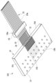
- FIG. 1 is a bottom perspective view of an optical device according to one embodiment of the present disclosure
- FIG. 2 is a top perspective view of the optical device shown in FIG. 1
- FIG. It is the perspective view which expanded a part shown in FIG. 1, and was seen from the upper surface.
- (a) is a top view of an optical fiber connecting portion
- (b) is a vertical cross-sectional view
- (c) is a horizontal cross-sectional view.
- (a) is a bottom view of an optical waveguide substrate
- (b) is a cross-sectional view.
- (a), (b), and (c) are diagrams for explaining the manufacturing process of the optical device.
- 6(a), (b), and (c) are diagrams for explaining the manufacturing process of the optical device following FIG. 6(c).
- FIG. 7B is a top perspective view of the optical device shown in FIG. 7B; FIG.
- FIG. 1 is a bottom perspective view of an optical device 100 according to an embodiment of the present disclosure
- FIG. 2 is a top perspective view of the optical device 100 shown in FIG. 1
- FIG. 3 is an enlarged view of area A shown in FIG. It is the perspective view seen from the upper surface.
- the upper and lower surfaces of this embodiment are defined by the coordinate system shown in FIG. 1, and the side with the larger z-axis coordinate is defined as "above” or "upper” with respect to the side with the smaller z-axis coordinate. Also, the side with the smaller z-axis coordinate is referred to as "below” or “lower” than the side with the larger z-axis coordinate.
- the lower surface 10a is the surface opposite to the surface of the optical waveguide substrate 10 of the optical device 100 from which the optical waveguide (not shown) can be seen.
- the upper surface 10b corresponds to the back surface of the lower surface 10a.
- a side surface 10c is defined between the upper surface 10a and the lower surface 10b.
- the side surface to which the optical fiber 23a is connected is particularly referred to as an end surface 10d.
- the reason why the side with the larger z-axis coordinate is the lower surface 10a and the side with the smaller z-axis coordinate is the upper surface 10b is that the connection and alignment of the optical fiber 23a in this embodiment are performed by turning the optical waveguide substrate 10 upside down. because it is done.
- the perspective views of FIGS. 1, 2, and 3 all show the state in which the optical fiber 23a is close to the end surface 10d, and the state in which the optical fiber 23a is connected to the optical waveguide in the optical waveguide substrate 10. not shown.
- the optical waveguide substrate 10 includes a substrate body 101 and an optical waveguide 102 formed in the substrate body.
- the substrate body includes one end surface 10d, and a through hole 12a that penetrates the substrate body in the thickness direction, communicates with the through hole 12a, and extends parallel to the main surface (for example, the lower surface 10a) of the substrate body 101. and a long groove portion 12b.
- the through hole 12a is formed at a position corresponding to the optical waveguide 102, and the inner surface of the long groove portion 12b is an inclined surface 12c that contacts the optical fiber 23a when the optical fiber 23a is inserted into the long groove portion 12b via the through hole 12a.
- Such a through hole 12a and long groove portion 12b constitute an optical fiber connecting portion 12, which will be described later.
- the through-hole 12a includes the end face 10d
- the through-hole 12a is not formed at a position included in the plane of the optical waveguide substrate 10, and the inner surface is open at the location where it intersects with the end surface 10d.
- the optical fiber 23a engages with the open inner surface of the through hole 12a and is aligned in the long groove portion 12b.
- the optical waveguide substrate 10 constitutes an optical device by further connecting the optical fiber 23a and the electronic circuit 3 (FIG. 5).
- the optical fiber 23a aligned by the through hole 12a is connected to the optical waveguide (not shown) of the optical waveguide substrate 10 with high precision, as will be described in detail later. Therefore, the through hole 12a is formed at a position corresponding to an optical waveguide (not shown). Therefore, in this embodiment, it is possible to indirectly confirm the position of the optical waveguide from the position of the through hole 12a. This point will also be described later.
- the optical waveguide substrate 10 may be a photonics substrate made of Si.
- the optical fiber 23 a is composed of a core layer 24 as an optical waveguide and a clad layer 25 protecting the core layer 24 .
- Each optical fiber 23 a is bundled by a glass block 26 to form an optical fiber group 23 .
- the glass block 26 is formed with a holding hole 26a for holding the inserted optical fiber 23a.
- the holding hole 26a has an elliptical vertical cross section, and the long axis is designed to be larger than the value obtained by multiplying the coating diameter of the optical fiber 23a by the number of cores.
- the optical fibers 23a inserted through the holding holes 26a are held parallel to each other at regular intervals.
- the crack layer 25 is exposed by partially removing the coating on the side of the optical fiber 23a facing the optical waveguide substrate 10 .
- a plurality of bumps 13 for flip-flop mounting are provided on the upper surface 10b of the optical waveguide substrate 10. As shown in FIG.
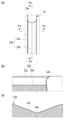
- FIGS. 4(a), 4(b), 4(c), 5(a) and 5(b) are diagrams for explaining the optical fiber connecting portion 12.
- FIG. 4(a) is a top view showing the optical fiber connection portion 12 seen from the side of the upper surface 10b of the optical waveguide substrate 10
- FIG. 4(b) is a sectional view taken along arrows IVb and IVb in FIG. 4(a).
- 4(c) is a sectional view taken along arrows IVc and IVc in FIG. 4(a).
- the long groove portion 12b has a vertical slope 12e and a slope 12c obliquely extending from the vertical angle 12e toward the lower surface 10a of the optical waveguide substrate.
- Consecutive vertices of the apex angle 12e coincide with the center line along the extending direction of the long groove portion 12b. Therefore, it can be said that the slope 12c is inclined from the center line along the extending direction of the long groove portion 12b toward the upper surface 10b (mounting surface) on which the electronic circuit 3 is mounted.
- the inclined surface 12c of this embodiment is a V-groove having a V-shaped cross section orthogonal to the extending direction of the long groove portion 12b.
- the optical fiber 23a comes into contact with the V-groove, is restricted from moving away from the apex angle 12e by the slopes 12c on both sides of the apex angle 12e, and is aligned with the apex angle 12e. be.
- FIG. 5(a) is a bottom view of the optical waveguide substrate 10 viewed from the bottom surface 10a
- FIG. 5(b) is a cross section along arrows Vb and Vb in FIG. 5(a).
- the optical fiber 23a is partially inserted into the through hole 12a and is not inserted into the long groove portion 12b.
- the edge of the through hole 12a of the present embodiment extends from the end surface 10d toward the extension direction of the long groove 12b in top view, forming an arc. , and is formed so as to face the end surface 12d again.
- Such a shape is also referred to as a "U-shape" in this embodiment.
- the electronic circuit 3 is mounted on the upper surface 10b of the optical waveguide substrate 10 via the bumps 13, as shown in FIG. 5(b). Therefore, the upper surface 10b of this embodiment corresponds to the mounting surface.
- the mounting of the electronic circuit 3 is performed before connection and alignment of the optical fiber 23a. Therefore, in this embodiment, the alignment of the plurality of optical fibers 23a with the through holes 12a is performed on the optical waveguide substrate 10 on which the electronic circuit 3 is mounted.
- the electronic path 3 can be mounted without the optical fiber 23a being connected, and the electronic circuit 3 can be easily mounted.
- the inner surface of the through hole 12a has a slope 12f inclined from the vertex of the apex angle 12c, that is, the center line along the extending direction of the long groove portion 12b toward the upper surface 10b, which is the mounting surface. is formed.
- a slope 12f comes into contact with the optical fibers 23a aligned in parallel and at regular intervals by the through holes 12a when the optical fibers 23a move downward, allowing the optical fibers 23a to smoothly pass through to the long groove portion 12b. It has a function of leading to the lower part of the hole 12a.
- the long groove portion 12b is formed at a position corresponding to the optical waveguide 102. As shown in FIG.
- the optical fiber 23a guided downward through the through-hole 12a advances along the long groove 12b, and its end surface is aligned with the end surface of the optical waveguide 102.
- the position where the long groove portion 12b and the optical waveguide 102 correspond means the position where the optical axis of the optical fiber 23a inserted into the long groove portion 23a and the optical axis of the optical waveguide 102 coincide. .
- the V-shaped long groove portion 12b can be formed by known photolithography and wet etching.
- the long groove portion 12b is formed in accordance with the position of the optical waveguide 102. As shown in FIG.
- the depth of the long groove portion 12 b is adjusted so that the center of the core layer 24 of the optical fiber 23 a matches the height of the optical waveguide 102 .
- by arranging the optical fiber 23a in the V groove of the long groove portion 12b it is possible to establish a low-loss optical connection while omitting the optical polishing process and the active alignment process.
- FIGS. 6(a), 6(b), 6(c), 7(a), 7(b) and 7(c) are for explaining each step of manufacturing the optical device 100.
- FIG. It is a diagram.
- a plurality of optical fibers 23a are passed through the holding holes 26a of the glass block 26 to form the optical fiber group 23.
- a portion of the optical fiber 23a directed toward the optical waveguide substrate 10 is removed from the covering material and cleave-cut.
- FIG. 6(b) the ends of the optical fiber groups 23 are slid into the through-holes 12a from above and aligned at regular intervals.
- the electronic circuit 3 is already mounted on the upper surface 10b as shown in FIGS. 6(b) and 6(c).
- the through hole 12a has a relatively gentle U-shape
- the optical fiber 23a moves downward along the optical waveguide substrate 10, as shown in FIG. 6(c).
- the apex of the convex portion of the U-shaped portion of the through hole 12a coincides with the apex of the apex angle 12e of the long groove portion 12b in the planar direction of the optical waveguide substrate 10 . Therefore, the optical fiber 23a that has moved downward smoothly descends toward the vertical angle of the V-shaped groove while contacting the inner surface of the through hole 12a.
- the optical fiber 23a slides along the slope 12f provided on the inner surface of the through hole 12a, and then smoothly loaded into the long groove portion 12b.
- the optical device manufacturing method of the present embodiment enables horizontal alignment between the optical fiber 23a and the optical waveguide.
- the optical fiber 23a may be inclined at an angle of 1 degree or more and 10 degrees or less with respect to the lower surface 10a of the optical waveguide substrate 10 when pushing the optical fiber 23a toward the long groove portion 12b.
- the inclination of the optical fiber 23a is preferably such that the optical fiber 23a faces upward from the lower surface 10a, that is, forms an elevation angle.
- FIG. 7(a) shows a state in which the glass block 26 is brought close to the end surface 10d of the optical waveguide substrate 10 after the optical fiber 23a is loaded.
- the position of the optical waveguide can be confirmed by the position of the through hole 12a.
- an ultraviolet (UV) curable adhesive 9 is dripped into the holding hole 26a of the glass block 26 and fixed by irradiating an appropriate amount of ultraviolet rays. be.
- the ultraviolet curable adhesive is filled in the through holes 12 a and the long grooves 12 b to firmly fix the optical fiber 23 a to the optical waveguide substrate 10 .
- FIG. 7(c) shows a state in which the entire holding hole 26a of the glass block 26 is filled with the ultraviolet curing adhesive 9.
- FIG. 8 shows the optical device shown in FIG. 7B as viewed from the side on which the electronic circuit 3 is mounted, ie, from the top surface 10b.
- the provision of the through holes 12a and the long grooves 12b allows the optical fiber to be aligned with the optical waveguide of the optical waveguide substrate at a proper angle. Therefore, according to the present embodiment, the accuracy of rough alignment between the optical waveguide and the optical fiber 23a can be improved more than the known technique, so that the time required for polishing or alignment of the optical waveguide and the optical fiber end surface can be shortened. can do. Also, since the through hole 12a is formed according to the position of the optical fiber aligned with the optical waveguide, it is necessarily formed at the position corresponding to the optical waveguide.
- the position of the optical waveguide can be confirmed from the side of the lower surface 10a of the optical device, and the work of aligning and connecting the optical fiber 23a can be facilitated.
- the work of aligning and connecting the optical fiber 23a may be performed manually by an operator. Further, it may be controlled automatically by a robot or the like, or by an operator while watching a monitor or the like.
Landscapes
- Physics & Mathematics (AREA)
- General Physics & Mathematics (AREA)
- Optics & Photonics (AREA)
- Optical Couplings Of Light Guides (AREA)
Abstract
L'invention concerne un substrat de guide d'ondes optique (10) comprenant un corps de substrat (101) et des guides d'ondes optiques (102) formés sur le corps de substrat (101) qui est configuré de telle sorte que : le corps de substrat (101) comprend des trous traversants (12a) qui comprennent une surface d'extrémité (10d) du corps de substrat (101) et qui pénètrent à travers le corps de substrat (101) dans le sens de l'épaisseur, et de longues parties de rainure (12b) qui sont contiguës aux trous traversants (12a) et qui s'étendent parallèlement à la surface principale du corps de substrat ; les trous traversants (12a) sont formés à des positions correspondant aux guides d'ondes optiques (102) ; et les surfaces internes des longues parties de rainure (12b) comprennent des surfaces inclinées (12c) qui entrent en contact avec des fibres optiques (23a) lorsque les fibres optiques (23a) sont insérées dans les longues parties de rainure (12b) à travers les trous traversants (12a).
Priority Applications (2)
| Application Number | Priority Date | Filing Date | Title |
|---|---|---|---|
| PCT/JP2021/045370 WO2023105717A1 (fr) | 2021-12-09 | 2021-12-09 | Substrat de guide d'ondes optique, dispositif optique et procédé de fabrication pour dispositif optique |
| JP2023565808A JPWO2023105717A1 (fr) | 2021-12-09 | 2021-12-09 |
Applications Claiming Priority (1)
| Application Number | Priority Date | Filing Date | Title |
|---|---|---|---|
| PCT/JP2021/045370 WO2023105717A1 (fr) | 2021-12-09 | 2021-12-09 | Substrat de guide d'ondes optique, dispositif optique et procédé de fabrication pour dispositif optique |
Publications (1)
| Publication Number | Publication Date |
|---|---|
| WO2023105717A1 true WO2023105717A1 (fr) | 2023-06-15 |
Family
ID=86730039
Family Applications (1)
| Application Number | Title | Priority Date | Filing Date |
|---|---|---|---|
| PCT/JP2021/045370 WO2023105717A1 (fr) | 2021-12-09 | 2021-12-09 | Substrat de guide d'ondes optique, dispositif optique et procédé de fabrication pour dispositif optique |
Country Status (2)
| Country | Link |
|---|---|
| JP (1) | JPWO2023105717A1 (fr) |
| WO (1) | WO2023105717A1 (fr) |
Citations (7)
| Publication number | Priority date | Publication date | Assignee | Title |
|---|---|---|---|---|
| JPS5834415A (ja) * | 1981-08-24 | 1983-02-28 | Nippon Telegr & Teleph Corp <Ntt> | 光導波路と光フアイバの結合方法 |
| JPH01302211A (ja) * | 1988-05-30 | 1989-12-06 | Nippon Telegr & Teleph Corp <Ntt> | 光導波路と光ファイバの固定構造及びその固定方法 |
| JPH0618728A (ja) * | 1992-07-02 | 1994-01-28 | Hitachi Cable Ltd | 光導波路及びその製造方法 |
| JPH0862438A (ja) * | 1994-08-24 | 1996-03-08 | Hitachi Cable Ltd | 光導波路及びその製造方法 |
| JP2016071034A (ja) * | 2014-09-29 | 2016-05-09 | 富士通株式会社 | 光ファイバガイド、光ファイバガイドを備えた光導波路基板、光入出力装置、及び光ファイバの実装方法 |
| JP2016167005A (ja) * | 2015-03-10 | 2016-09-15 | 富士通株式会社 | 光学装置及び光学装置の製造方法 |
| US20190271810A1 (en) * | 2018-01-25 | 2019-09-05 | Poet Technologies, Inc. | Optical dielectric planar waveguide process |
-
2021
- 2021-12-09 JP JP2023565808A patent/JPWO2023105717A1/ja active Pending
- 2021-12-09 WO PCT/JP2021/045370 patent/WO2023105717A1/fr unknown
Patent Citations (7)
| Publication number | Priority date | Publication date | Assignee | Title |
|---|---|---|---|---|
| JPS5834415A (ja) * | 1981-08-24 | 1983-02-28 | Nippon Telegr & Teleph Corp <Ntt> | 光導波路と光フアイバの結合方法 |
| JPH01302211A (ja) * | 1988-05-30 | 1989-12-06 | Nippon Telegr & Teleph Corp <Ntt> | 光導波路と光ファイバの固定構造及びその固定方法 |
| JPH0618728A (ja) * | 1992-07-02 | 1994-01-28 | Hitachi Cable Ltd | 光導波路及びその製造方法 |
| JPH0862438A (ja) * | 1994-08-24 | 1996-03-08 | Hitachi Cable Ltd | 光導波路及びその製造方法 |
| JP2016071034A (ja) * | 2014-09-29 | 2016-05-09 | 富士通株式会社 | 光ファイバガイド、光ファイバガイドを備えた光導波路基板、光入出力装置、及び光ファイバの実装方法 |
| JP2016167005A (ja) * | 2015-03-10 | 2016-09-15 | 富士通株式会社 | 光学装置及び光学装置の製造方法 |
| US20190271810A1 (en) * | 2018-01-25 | 2019-09-05 | Poet Technologies, Inc. | Optical dielectric planar waveguide process |
Also Published As
| Publication number | Publication date |
|---|---|
| JPWO2023105717A1 (fr) | 2023-06-15 |
Similar Documents
| Publication | Publication Date | Title |
|---|---|---|
| KR960014123B1 (ko) | 광도파로와 광파이버의 접속방법 | |
| EP3171206B1 (fr) | Dispositifs d'interface optique et procédés utilisant des fibres optiques et un élément de support ayant une section coudée | |
| JPH05333231A (ja) | 光導波路と光ファイバの接続方法 | |
| US6728450B2 (en) | Alignment of optical fibers with an optical device | |
| US10162112B2 (en) | Optical wire bond apparatus and methods employing laser-written waveguides | |
| US11422321B2 (en) | Optical fiber connection component and optical device manufacturing method | |
| KR100442609B1 (ko) | 플립칩 본딩구조 및 본딩방법 | |
| US20160091667A1 (en) | Optical fiber guide, optical waveguide substrate comprising optical fiber guide, optical input-output device, and optical fiber mounting method | |
| JPH09178962A (ja) | 光ファイバアレイおよびその製造法 | |
| CN108508545B (zh) | 光学器件的耦合结构及耦合方法 | |
| US20030142920A1 (en) | Method and apparatus for optical fiber array assembly | |
| WO2023105717A1 (fr) | Substrat de guide d'ondes optique, dispositif optique et procédé de fabrication pour dispositif optique | |
| US6907178B2 (en) | Optoelectronic assembly with embedded optical and electrical components | |
| KR19990061766A (ko) | 광섬유 및 광도파로 소자 접속 구조 | |
| US20030142921A1 (en) | Method of aligning optical fibers in an array member | |
| US10564370B2 (en) | Optical connecting device, light processing apparatus, method for fabricating optical connecting device | |
| JP2004006879A (ja) | 光モジュール光軸整列方法 | |
| WO2024033988A1 (fr) | Structure de connexion entre une fibre optique et un guide d'ondes optique, et procédé de fabrication d'un substrat de guide d'ondes optique | |
| US7076136B1 (en) | Method of attaching optical fibers to integrated optic chips that excludes all adhesive from the optical path | |
| WO2023275990A1 (fr) | Procédé de fabrication de dispositif de guide d'ondes optique et dispositif de guide d'ondes optique | |
| JPH06118275A (ja) | 光接続部品及びその製造方法 | |
| WO2022003880A1 (fr) | Composant optique | |
| CN1502054A (zh) | 光学装置 | |
| KR100450945B1 (ko) | 광모듈의 정렬 및 고정 방법 | |
| JP4915505B2 (ja) | 光基板の製造方法 |
Legal Events
| Date | Code | Title | Description |
|---|---|---|---|
| 121 | Ep: the epo has been informed by wipo that ep was designated in this application |
Ref document number: 21967213 Country of ref document: EP Kind code of ref document: A1 |
|
| ENP | Entry into the national phase |
Ref document number: 2023565808 Country of ref document: JP Kind code of ref document: A |
|
| NENP | Non-entry into the national phase |
Ref country code: DE |