WO2023100517A1 - 回路モジュール - Google Patents
回路モジュール Download PDFInfo
- Publication number
- WO2023100517A1 WO2023100517A1 PCT/JP2022/039103 JP2022039103W WO2023100517A1 WO 2023100517 A1 WO2023100517 A1 WO 2023100517A1 JP 2022039103 W JP2022039103 W JP 2022039103W WO 2023100517 A1 WO2023100517 A1 WO 2023100517A1
- Authority
- WO
- WIPO (PCT)
- Prior art keywords
- circuit module
- stud
- electrode
- stud electrode
- mold resin
- Prior art date
- Legal status (The legal status is an assumption and is not a legal conclusion. Google has not performed a legal analysis and makes no representation as to the accuracy of the status listed.)
- Ceased
Links
Images








Classifications
-
- H—ELECTRICITY
- H05—ELECTRIC TECHNIQUES NOT OTHERWISE PROVIDED FOR
- H05K—PRINTED CIRCUITS; CASINGS OR CONSTRUCTIONAL DETAILS OF ELECTRIC APPARATUS; MANUFACTURE OF ASSEMBLAGES OF ELECTRICAL COMPONENTS
- H05K1/00—Printed circuits
- H05K1/02—Details
- H05K1/11—Printed elements for providing electric connections to or between printed circuits
-
- H—ELECTRICITY
- H05—ELECTRIC TECHNIQUES NOT OTHERWISE PROVIDED FOR
- H05K—PRINTED CIRCUITS; CASINGS OR CONSTRUCTIONAL DETAILS OF ELECTRIC APPARATUS; MANUFACTURE OF ASSEMBLAGES OF ELECTRICAL COMPONENTS
- H05K3/00—Apparatus or processes for manufacturing printed circuits
- H05K3/22—Secondary treatment of printed circuits
- H05K3/28—Applying non-metallic protective coatings
-
- H—ELECTRICITY
- H05—ELECTRIC TECHNIQUES NOT OTHERWISE PROVIDED FOR
- H05K—PRINTED CIRCUITS; CASINGS OR CONSTRUCTIONAL DETAILS OF ELECTRIC APPARATUS; MANUFACTURE OF ASSEMBLAGES OF ELECTRICAL COMPONENTS
- H05K3/00—Apparatus or processes for manufacturing printed circuits
- H05K3/30—Assembling printed circuits with electric components, e.g. with resistors
- H05K3/32—Assembling printed circuits with electric components, e.g. with resistors electrically connecting electric components or wires to printed circuits
- H05K3/34—Assembling printed circuits with electric components, e.g. with resistors electrically connecting electric components or wires to printed circuits by soldering
-
- H—ELECTRICITY
- H10—SEMICONDUCTOR DEVICES; ELECTRIC SOLID-STATE DEVICES NOT OTHERWISE PROVIDED FOR
- H10W—GENERIC PACKAGES, INTERCONNECTIONS, CONNECTORS OR OTHER CONSTRUCTIONAL DETAILS OF DEVICES COVERED BY CLASS H10
- H10W74/00—Encapsulations, e.g. protective coatings
Definitions
- the present invention relates to circuit modules.
- a circuit module that mounts components on a substrate and then covers the components with mold resin is widely used.
- stud electrodes are used to connect wiring formed on the substrate to external electronic components. That is, a circuit module is manufactured in which the end of the stud electrode on the substrate side is connected to the wiring formed on the substrate, and the other end is exposed from the mold resin. By mounting the circuit module on the external electronic component through the other end of the stud electrode, the wiring formed on the substrate and the external electronic component can be electrically connected.
- Patent Document 1 discloses a substrate having a first surface, a first component and a second component mounted on the first surface, and the first component and the Formed on the first surface so as to cover a first conductive material (stud electrode) mounted between the second component and the first component, the second component and the first conductive material (stud electrode) and a first shield film covering a surface of the first sealing resin (mold resin) farther from the substrate, the first sealing resin (mold resin) ) has a recess so as to expose at least a part of the first conductive material (stud electrode), and the first shield film extends along the inner surface of the recess so that the first conductive material (stud electrode), an opening is provided in the first shield film in the recess, a metal bump is disposed inside the recess, and the metal bump is connected to the A module (circuit module) is disclosed which is electrically connected to said first conductive material (stud electrode) through an aperture.
- a module circuit module
- solder bumps are used to connect the first conductive material (stud electrode) and the external electronic component.
- the solder bumps are easily separated from the first conductive material (stud electrode). There was a problem that it peeled off.
- the present invention was made to solve the above problems, and an object of the present invention is to provide a circuit module in which solder bumps are less likely to come off from stud electrodes.
- a circuit module of the present invention comprises a substrate, a mold resin having a first main surface arranged on the surface of the substrate and in contact with the surface of the substrate, and a second main surface facing the first main surface; a stud electrode arranged on the surface of the substrate and surrounded by the mold resin;
- the stud electrode has an exposed end surface and an exposed side surface exposed from the mold resin, and a plating layer is formed on the exposed side surface.
- FIG. 1A is a cross-sectional view schematically showing an example of a circuit module according to a first embodiment of the present invention
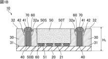
- FIG. 1B is a cross-sectional view schematically showing an example of a state in which solder bumps are arranged on stud electrodes of the circuit module according to the first embodiment of the present invention.
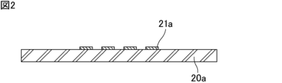
- FIG. 2 is a process diagram schematically showing an example of the ceramic green sheet preparation process in the circuit module manufacturing method according to the first embodiment of the present invention.
- FIG. 3 is a process diagram schematically showing an example of the stud electrode constraining layer preparation process in the circuit module manufacturing method according to the first embodiment of the present invention.
- FIG. 1A is a cross-sectional view schematically showing an example of a circuit module according to a first embodiment of the present invention
- FIG. 1B is a cross-sectional view schematically showing an example of a state in which solder bumps are arranged on stud electrodes of the circuit module according to the first embodiment of the present invention.
- FIG. 2 is
- FIG. 4 is a process diagram schematically showing an example of a constraining layer lamination process for stud electrodes in the method of manufacturing a circuit module according to the first embodiment of the present invention.
- FIG. 5 is a process diagram schematically showing an example of the firing process in the method of manufacturing the circuit module according to the first embodiment of the present invention.
- FIG. 6 is a process diagram schematically showing an example of a stud electrode constraining layer removing process in the circuit module manufacturing method according to the first embodiment of the present invention.
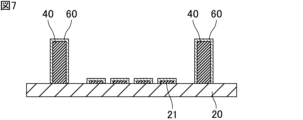
- FIG. 7 is a process diagram schematically showing an example of the plating process in the method of manufacturing the circuit module according to the first embodiment of the present invention.
- FIG. 8 is a process diagram schematically showing an example of an electronic component placement process in the method of manufacturing a circuit module according to the first embodiment of the present invention.
- FIG. 9 is a process diagram schematically showing an example of the resin sealing process in the method of manufacturing the circuit module according to the first embodiment of the present invention.
- FIG. 10 is a process diagram schematically showing an example of the polishing process in the method of manufacturing the circuit module according to the first embodiment of the present invention.
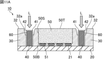
- FIG. 11A is a process diagram schematically showing an example of a stud electrode exposing process in the circuit module manufacturing method according to the first embodiment of the present invention.
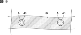
- FIG. 11B is a plan view of the second main surface of the mold resin schematically showing an example of laser irradiation positions in the stud electrode exposing step.
- FIG. 12A is a cross-sectional view schematically showing an example of a state in which solder bumps are arranged on the circuit module according to the first embodiment of the present invention
- FIG. 12B is a cross-sectional view schematically showing an example of a state in which solder bumps arranged on the circuit module according to the first embodiment of the present invention are melted by reflow
- FIG. FIG. 13 is a cross-sectional view schematically showing an example of a modification of the circuit module according to the first embodiment of the invention.
- FIG. 14 is a cross-sectional view schematically showing another modified example of the circuit module according to the first embodiment of the present invention.
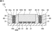
- FIG. 15 is a cross-sectional view schematically showing another example of the circuit module according to the second embodiment of the invention.
- FIG. 16 is a cross-sectional view schematically showing an example of a circuit module according to another embodiment of the invention.
- circuit module of the present invention will be described below.
- the present invention is not limited to the following configurations, and can be appropriately modified and applied without changing the gist of the present invention. Combinations of two or more of the individual preferred configurations of the invention described below are also the invention.
- a circuit module of the present invention comprises a substrate, a mold resin having a first main surface arranged on the surface of the substrate and in contact with the surface of the substrate, and a second main surface facing the first main surface; a stud electrode arranged on the surface of the substrate and surrounded by the mold resin; In the above, the stud electrode has an exposed end surface and an exposed side surface exposed from the mold resin, and a plating layer is formed on the exposed side surface.
- the circuit module of the present invention may have other configurations as long as the above configuration is included, as long as the effects of the present invention are exhibited.
- FIG. 1A is a cross-sectional view schematically showing an example of a circuit module according to a first embodiment;
- the circuit module 10 shown in FIG. 1A includes a substrate 20, a first main surface 31 arranged on the surface of the substrate 20 and in contact with the surface of the substrate 20, and a second main surface 32 facing the first main surface 31. and a stud electrode 40 arranged on the surface of the substrate 20 and covered with the mold resin 30 .
- wiring is formed on the substrate 20, and the wiring and the stud electrode 40 are connected.
- the electronic component 50 is arranged on the electrode 21 formed on the surface of the substrate 20 via the connection member 51 .
- Electronic component 50 has bottom surface 50 ⁇ /b>B and side surface 50 ⁇ /b>S connected to electrodes 21 covered with mold resin 30 , and top surface 50 ⁇ /b>T exposed from mold resin 30 .
- the upper surface 50T of the electronic component 50 is located on the same plane as the second main surface 32 of the mold resin 30 .
- the mold resin 30 has a recessed portion 32a formed so that a portion of the second main surface 32 is recessed.
- the stud electrode 40 has an exposed end surface 41 and an exposed side surface 42 exposed from the mold resin 30 in the recess 32a.
- a plating layer 60 is formed on the surface of the stud electrode 40 including the electrode 21 and the exposed end surface 41 and the exposed side surface 42 .
- the exposed end surface 41 is located closer to the substrate 20 than the second main surface 32 is.
- FIG. 1B is a cross-sectional view schematically showing an example of a state in which solder bumps are arranged on stud electrodes of the circuit module according to the first embodiment of the present invention.
- the solder bumps 70 are arranged in the recesses 32a of the second main surface 32.
- the solder bumps 70 are heated to be melted and connected to the stud electrodes 40 .
- the solder bump 70 melts, it wets and spreads not only on the exposed end surface 41 of the stud electrode 40 but also on the exposed side surface 42 .
- the solder bumps 70 will cool and harden, but the solder bumps 70 will connect not only the exposed end surfaces 41 of the stud electrodes 40 but also the exposed side surfaces 42 .
- solder bumps In the conventional circuit module, only the end faces of the stud electrodes are exposed from the molding resin. Therefore, when solder bumps are arranged on a conventional circuit module, the solder bumps are connected only to the ends of the stud electrodes. However, as described above, in the circuit module 10 , the solder bumps 70 connect not only the exposed end surfaces 41 of the stud electrodes 40 but also the exposed side surfaces 42 . Therefore, the contact area between the solder bumps 70 and the stud electrodes 40 becomes larger than when solder bumps are arranged in a conventional circuit module. Therefore, solder bumps 70 are less likely to come off from stud electrodes 40 .
- the solder bumps 70 continuously cover both the exposed end surface 41 and the exposed side surface 42 of the stud electrode 40 .
- the solder bump 70 straddles the corner of the stud electrode 40 and continuously covers the exposed end surface 41 and the exposed side surface 42 .
- the area of the interface can be increased.
- the interface between the solder bump 70 and the stud electrode 40 is curved at the corner of the stud electrode 40 and is not flat. Therefore, even if stress is generated at the interface between the solder bump 70 and the stud electrode 40, the stress can be received at a plurality of portions, making it difficult for the stress to concentrate.
- the stress tends to concentrate on the corners of the stud electrode 40, but since the solder bump 70 covers the corners of the stud electrode 40 so as to straddle the corners, the stress is less likely to concentrate. For this reason as well, the solder bumps 70 are less likely to come off from the stud electrodes 40 .
- the plating layer 60 is formed on the exposed end surface 41 and the exposed side surface 42 of the stud electrode 40 .
- the wettability of the solder bumps 70 can be improved. Therefore, solder bumps 70 can be made less likely to come off from stud electrodes 40 .
- the exposed end surface 41 is positioned closer to the substrate 20 than the second main surface 32 of the mold resin 30 .
- the solder bumps 70 are arranged in the recesses 32a, the bottoms of the solder bumps 70 come into contact with the exposed end surfaces 41 of the stud electrodes 40.
- the exposed end face 41 is positioned closer to the substrate 20 than the second main surface 32 of the mold resin 30, so the solder bump 70 enters the recess 32a. Then, the distance from the bottom of the substrate 20 to the top of the solder bumps 70 can be shortened. That is, the height of the circuit module 10 when the solder bumps 70 are arranged (the height indicated by symbol "H 1 " in FIG. 1B) can be reduced.
- circuit module 10 Each configuration of the circuit module 10 will be described in detail below.
- the substrate 20 is not particularly limited, but is preferably a ceramic substrate formed by firing a ceramic green sheet made of a low temperature co-fired ceramic (LTCC) material.
- LTCC low temperature co-fired ceramic
- a low-temperature sintering ceramic material is one type of ceramic material, and is a ceramic material that can be sintered at a temperature of 1000° C. or less and can be co-fired with Au, Ag, Cu, or the like having a low specific resistance.
- low-temperature sintered ceramic materials include glass composite low-temperature sintered ceramic materials obtained by mixing ceramic powders such as alumina, zirconia, magnesia, and forsterite with borosilicate glass, and ZnO—MgO—Al 2 Crystallized glass-based low-temperature sintered ceramic materials using O 3 —SiO 2 -based crystallized glass, BaO—Al 2 O 3 —SiO 2 based ceramic powders and Al 2 O 3 —CaO—SiO 2 —MgO—B 2
- Non-glass-based low-temperature sintered ceramic materials using O 3 -based ceramic powder and the like are included.
- the thickness of the substrate 20 is preferably 5 ⁇ m or more and 100 ⁇ m or less, for example.
- a plating layer 60 is formed on the electrodes 21 arranged on the surface of the substrate 20 .
- the electrode 21 is preferably made of a metal material such as Cu or Cu alloy.
- the plating layer 60 formed on the electrode 21 is preferably made of a metal material such as Ni or Ni alloy.
- FIG. 1A illustrates a single-layer substrate as the substrate 20 of the circuit module 10, but in the circuit module of the present invention, the substrate may be a laminated substrate in which a plurality of substrates are laminated. Further, internal electrodes and vias may be formed inside the stacked substrates. Furthermore, in the circuit module of the present invention, another substrate may be laminated under the substrate 20.
- the other substrate may be a ceramic substrate or a resin substrate.
- the mold resin is preferably a resin composition in which a filler such as a glass material or silica is dispersed in a resin material.
- a filler such as a glass material or silica
- Epoxy resin, silicone, phenol resin, or the like can be used as the resin material.
- the thickness of the mold resin 30 is preferably set appropriately according to the application of the circuit module, and is, for example, 0.05 mm or more and 0.30 mm or less. is preferred.
- the mold resin 30 has a recessed portion 32a formed so that a portion of the second main surface 32 is recessed. By forming the concave portion 32a, the side surface of the stud electrode 40 can be exposed and the exposed side surface 42 can be formed.
- the shape of the concave portion 32a is not particularly limited, but when viewed from the direction perpendicular to the second main surface 32, it may be circular, elliptical, triangular, quadrangular, pentagonal, hexagonal, octagonal, or the like. There may be.
- the area inside the outline of the bottom surface of the recess 32a on the second main surface 32 when viewed from the direction perpendicular to the second main surface 32 is preferably set appropriately according to the size of the stud electrode 40, etc. For example, it is preferably 0.03 mm 2 or more and 0.30 mm 2 or less.
- the recess 32a has a tapered shape in which the wall surface is formed obliquely with respect to the bottom surface. may be vertical.
- the depth of the concave portion 32a in the thickness direction of the mold resin 30 is preferably 10% or more and 50% or less of the thickness T of the mold resin 30. It is more preferably 20% or more and 45% or less. If the depth of the recess is less than 10% of the thickness T of the mold resin, the area of the exposed side surface of the stud electrode becomes small, making it difficult to obtain the effect of preventing the solder bump from peeling off from the stud electrode. If the depth of the recess exceeds 50% of the thickness T of the mold resin, the difficulty of forming the recess increases, and the productivity of the circuit module tends to decrease. Further, when forming such recesses by laser processing, a high output is required, which may damage the plating layer formed on the stud electrode. Furthermore, it becomes difficult to remove the resin residue by the desmear process.
- the material constituting the stud electrode 40 is not particularly limited, for example, a metal material such as Cu or a Cu alloy can be used.
- Cu alloys include, for example, Cu-10Ni alloys.
- the stud electrode 40 is preferably a sintered body obtained by sintering these metal powders. If the substrate 20 is a ceramic substrate, the stud electrodes 40 can be formed together when the ceramic substrate is sintered. Therefore, in the process of manufacturing the circuit module 10, the number of times of heating can be reduced, so that damage to the circuit module 10 due to heat can be reduced.
- the shape of the stud electrode 40 is not particularly limited, but may be cylindrical, elliptical, triangular, square, pentagonal, hexagonal, or octagonal. Among these, a columnar shape is preferable.
- the area of the exposed end face 41 of the stud electrode 40 is preferably 0.10 mm 2 or more and 0.28 mm 2 or less, more preferably 0.13 mm 2 or more and 0.26 mm 2 or less.
- the height of the stud electrode 40 (the height indicated by symbol “H 2 ” in FIG. 1A) is preferably 0.055 mm or more and 0.290 mm or less, and is 0.060 mm or more and 0.280 mm or less. is more preferred.
- the height of the exposed side surface 42 of the stud electrode 40 in the thickness direction of the mold resin 30 is 5% or more and 30% or less of the thickness T of the mold resin 30 . preferably 10% or more and 25% or less. If the height H3 of the exposed side surface is less than 5% of the thickness T of the mold resin, the area of the exposed side surface becomes small, making it difficult to obtain the effect of preventing the solder bump from peeling off from the stud electrode. In order for the height H3 of the exposed side surface 42 to exceed 30% of the thickness T of the mold resin 30, it is necessary to form a deep recess. However, when forming such a deep recess, the degree of processing difficulty increases, and the productivity of the circuit module tends to decrease.
- the height H3 of the exposed side surface 42 of the stud electrode 40 in the thickness direction of the mold resin 30 is preferably 20% or more and 80% or less of the depth D of the recess 32a. Within this range, the exposed side surface 42 of the stud electrode 40 and the solder bump 70 can be preferably connected.
- the plating layer 60 formed on the stud electrode 40 is not particularly limited, it is preferably made of metals such as Ni, Au, Cu, Pd, Ag, Sn, and alloys thereof. When the plating layer 60 is made of these metals, the wettability of the solder bumps 70 is improved. As a result, solder bumps 70 are preferably connected to exposed end surfaces 41 and exposed side surfaces 42 of stud electrodes 40 . Furthermore, the plating layer 60 can protect the stud electrode 40 and prevent it from being corroded.
- the plated layer 60 may be formed by electroless plating or electrolytic plating.
- the thickness of the plating layer 60 is preferably 2 ⁇ m or more and 15 ⁇ m or less. Within such a range, the plating layer 60 can suitably protect the stud electrode 40 and prevent corrosion and the like.
- the electronic component 50 is preferably, for example, chip components such as multilayer capacitors, multilayer inductors, and various filters, and semiconductor components such as various ICs and memories.
- the electronic component 50 is connected to the electrode 21, but the connection method is not particularly limited, and may be connected by a connecting member such as Sn--Ag--Cu based Pb-free solder.
- solder bumps 70 can be conventionally known solder bumps. As such a solder bump 70, for example, Sn--Ag--Cu based Pb-free solder can be used.
- circuit module 10 Next, a method for manufacturing the circuit module 10 will be described. In the manufacturing method below, a case of manufacturing a ceramic substrate using an LTCC material as the substrate will be described.
- the method of manufacturing the circuit module 10 includes a ceramic green sheet preparation step, a stud electrode constrained layer preparation step, a stud electrode constrained layer lamination step, a firing step, a stud electrode constrained layer removal step, a plating step, an electronic component placement step, a resin A sealing step, a polishing step, and a stud electrode exposing step may be included.
- FIG. 2 is a process diagram schematically showing an example of the ceramic green sheet preparation process in the circuit module manufacturing method according to the first embodiment of the present invention.
- an LTCC material, a binder, and a plasticizer are mixed in arbitrary amounts to prepare a slurry.
- the slurry is applied onto a carrier film to form a ceramic green sheet 20a shown in FIG.
- a lip coater or a doctor blade can be used to apply the slurry. It is preferable to mold the slurry with a thickness of 5 to 100 ⁇ m.
- a conductive powder, a plasticizer and a binder are mixed to prepare a conductive paste for circuit formation, and the conductive paste for circuit formation is printed on the surface of the ceramic green sheet 20a to form an unfired wiring pattern ( (not shown) and an electrode green body 21a.
- Screen printing, inkjet printing, gravure printing and the like can be used as printing methods. Through such steps, the ceramic green sheet 20a shown in FIG. 2 can be prepared.
- FIG. 3 is a process diagram schematically showing an example of the stud electrode constraining layer preparation process in the circuit module manufacturing method according to the first embodiment of the present invention.
- an LTCC material, a hard-to-sinter ceramic material powder, a binder, and a plasticizer are mixed to prepare a slurry.
- the hard-to-sinter ceramic material powder for example, Al 2 O 3 or the like can be used.
- the difficult-to-sinter ceramic material is not substantially sintered at the sintering temperature of the LTCC material, and remains brittle even after firing. can do.
- the slurry is applied onto a carrier film to form a plurality of constraining layer green sheets 80a.
- a lip coater or a doctor blade can be used to apply the slurry. It is preferable to mold the slurry with a thickness of 5 ⁇ m or more and 100 ⁇ m or less.
- a through hole 81 is formed in the constraining layer green sheet 80a. The through holes 81 are formed at positions where the constraining layer green sheets 80a are exactly overlapped when they are laminated.
- a conductive powder, a plasticizer and a binder are mixed to prepare a conductive paste for forming stud electrodes. After that, as shown in FIG.
- the stud electrode forming conductive paste 40a is filled into the through holes 81 of the constraining layer green sheet 80a to form a plurality of stud electrode constraining layers 83 .
- the filling of the stud electrode forming conductive paste 40a can be performed by a known method such as screen printing.
- FIG. 4 is a process diagram schematically showing an example of a constraining layer lamination process for stud electrodes in the method of manufacturing a circuit module according to the first embodiment of the present invention.
- the ceramic green sheets 20a and the stud electrode constraining layers 83 are laminated.
- the stud electrode forming conductive paste 40a placed on each stud electrode constraining layer 83 is aligned so as to overlap the circuit (not shown) formed on the ceramic green sheet 20a.
- FIG. 5 is a process diagram schematically showing an example of the firing process in the method of manufacturing the circuit module according to the first embodiment of the present invention.
- the stacked ceramic green sheets 20a and the stud electrode constraining layers 83 are fired.
- the firing conditions are not particularly limited, and are preferably set appropriately according to the materials, shapes, etc. of the ceramic green sheets, circuit-forming conductive paste, and stud electrode conductive paste.
- the conductive paste for circuit formation and the conductive paste for stud electrodes contain a copper compound, they are preferably fired in a reducing atmosphere.
- a batch furnace or a belt furnace can be used as a firing furnace for firing.
- the ceramic green sheet 20a, the unfired electrode body 21a, and the stud electrode forming conductive paste 40a are fired into the substrate 20, the electrode 21, and the stud electrode 40, as shown in FIG.
- the constraining layer green sheet 80a is also sintered to become the constraining layer sheet 80 after sintering.
- the height of the stud electrode 40 can be adjusted by changing the thickness and the number of the stud electrode constraining layers 83 . In this process, the height of the head of the stud electrode 40 to be formed is made lower than the height of the head of the electronic component 50 arranged on the substrate, which will be described later.
- the substrate 20, the electrodes 21 and the stud electrodes 40 are collectively formed by one firing process. Therefore, in manufacturing the circuit module 10, the number of times of heating can be reduced.
- the stud electrode 40 is formed by stacking a plurality of stud electrode constraining layers 83, so that the stud electrode 40 can be easily formed at an accurate position.
- FIG. 6 is a process diagram schematically showing an example of a stud electrode constraining layer removing process in the circuit module manufacturing method according to the first embodiment of the present invention.
- the post-fired constraining layer sheet 80 is removed.
- a method for removing the constraining layer sheet 80 after firing is not particularly limited, but a known method such as sandblasting can be employed.
- FIG. 7 is a process diagram schematically showing an example of the plating process in the method of manufacturing the circuit module according to the first embodiment of the present invention.
- the surfaces of the stud electrode 40 and the electrode 21 are plated.
- a plated layer 60 can be formed on the surfaces of the stud electrode 40 and the electrode 21, as shown in FIG.
- the method of forming the plating layer 60 is not particularly limited, it is preferably formed by a known electroless plating method.
- FIG. 8 is a process diagram schematically showing an example of an electronic component placement process in the method of manufacturing a circuit module according to the first embodiment of the present invention.
- electronic components 50 are placed on the substrate 20 by connecting them to the electrodes 21 .
- FIG. 9 is a process diagram schematically showing an example of the resin sealing process in the method of manufacturing the circuit module according to the first embodiment of the present invention.
- the molding resin 30 is applied onto the substrate 20 so as to entirely cover the electronic component 50 connected to the stud electrodes 40 and the electrodes 21 .
- a known method can be adopted for applying the mold resin 30 .
- a portion of the mold resin 30 in contact with the surface of the substrate 20 serves as a first main surface 31 .
- the main surface facing the first main surface 31 is the second' main surface 32'.
- FIG. 10 is a process diagram schematically showing an example of the polishing process in the method of manufacturing the circuit module according to the first embodiment of the present invention.
- the mold resin 30 is polished from the second' main surface 32' side.
- part of the electronic component 50 is also polished.
- the head of the stud electrode 40 should not be polished.
- the polished surface of the mold resin 30 after polishing becomes the second main surface 32 .
- the second main surface 32 and the upper surface 50T of the electronic component 50 can be positioned on the same plane.
- a polishing method a known method such as lapping can be adopted.
- FIG. 11A is a process diagram schematically showing an example of a stud electrode exposing process in the circuit module manufacturing method according to the first embodiment of the present invention.
- part of the mold resin 30 is decomposed to form the concave portion 32a.
- a recess is formed so that a part of the stud electrode 40 is exposed.
- the exposed head portion of the stud electrode 40 becomes an exposed end surface 41
- the exposed side surface of the stud electrode 40 becomes an exposed side surface 42 .
- FIG. 11B is a plan view of the second main surface of the mold resin schematically showing an example of laser irradiation positions in the stud electrode exposing step.
- the laser irradiation range A is a range that covers the outline of the buried stud electrode 40 on the second main surface 32 (the range indicated by symbol “A” in FIG. 11B). preferable. By irradiating the laser in such a range, the side surface of the stud electrode 40 can also be exposed.
- a YAG laser for example, can be used as the laser.
- the output of the laser can decompose the mold resin 30, it should be adjusted so as not to damage the plating layer 60 formed on the exposed end surface 41 and the exposed side surface 42 of the stud electrode 40 and the stud electrode 40. is preferred.
- the laser irradiation After the laser irradiation, it is preferable to wash the laser-irradiated part by desmear treatment or the like to remove foreign matter.
- the circuit module 10 can be manufactured through the above steps.
- FIG. 12A is a cross-sectional view schematically showing an example of a state in which solder bumps are arranged on the circuit module according to the first embodiment of the present invention
- FIG. 12B is a cross-sectional view schematically showing an example of a state in which solder bumps arranged on the circuit module according to the first embodiment of the present invention are melted by reflow
- FIG. 12A solder bumps 70 are placed in the recesses 32a of the circuit module 10.
- FIG. 12B the solder bumps 70 are melted by reflow or the like.
- the reflow conditions are not particularly limited as long as the solder bumps 70 are melted.
- solder bumps 70 and the mold resin 30 are not bonded, a slight gap remains in the concave portion 32a.
- the solder bump 70 and the plated layer 60 formed on the stud electrode 40 form an alloy and join together.
- the solder bumps 70 melt, the solder bumps 70 also wet and spread on the exposed side surfaces 42 .
- the height of the solder bump 70 protruding from the concave portion 32a (the height indicated by symbol “H 4 ” in FIG. 12B) ) can be adjusted.
- FIG. 13 is a cross-sectional view schematically showing a modification of the circuit module according to the first embodiment of the invention.
- a circuit module 11 shown in FIG. 13 has an exposed end surface 41 of a stud electrode 40 located on the same plane as the second main surface 32, and has no plating layer 60 formed on the exposed end surface 41.
- the circuit module 11 shown in FIG. It has the same configuration as 10.
- the height H2 of the stud electrode 40 produced in the stud electrode constraining layer preparation step, the stud electrode constraining layer laminating step and the firing step is set to the height H2 of the circuit to be manufactured.
- a method of raising the height above the second main surface 32 of the module 11 and polishing the stud electrode 40 together with the mold resin 30 and the electronic component 50 in the above-described polishing process may be used.
- FIG. 14 is a cross-sectional view schematically showing another modification of the circuit module according to the first embodiment of the invention.
- a circuit module 12 shown in FIG. 14 has the same configuration as the circuit module 11 except that a plated layer 61 is formed on the exposed end surface 41 of the stud electrode 40 .
- the circuit module 12 can be manufactured by plating the exposed end faces 41 of the stud electrodes 40 in the circuit module 11 to form the plating layer 61 .
- the plating layer 60 and the plating layer 61 may be made of the same kind of metal, or may be made of different kinds of metal.
- FIG. 15 is a cross-sectional view schematically showing another example of the circuit module according to the second embodiment of the invention.
- a circuit module 110 shown in FIG. 15 has the same configuration as the circuit module 10 except that the stud electrodes 140 are porous.
- the molding resin thermally expands and pushes the stud electrodes.
- the stud electrodes themselves also thermally expand, and thermal stress is generated in the entire circuit module.
- the thermal stress may cause cracks inside the stud electrodes or at the joint interface between the mold resin and the solder bumps, or peeling between the stud electrodes and the mold resin.
- the stud electrodes 140 are porous as in the circuit module 110, the stud electrodes 140 are highly flexible and can absorb thermal stress. Therefore, for example, even if the mold resin 30 expands due to heat, the stud electrode 140 can absorb the expanded volume. Therefore, it is possible to prevent the above-mentioned cracks and peeling from occurring. That is, by making the stud electrodes 140 porous, the heat resistance of the module circuit is improved.
- Stud electrode 140 preferably has an internal porosity of 5 vol % or more and 40 vol % or less, more preferably 10 vol % or more and 35 vol % or less.
- the porosity is less than 5 vol %, it becomes difficult to sufficiently improve the heat resistance. If the porosity exceeds 40 vol %, the denseness of the stud electrode becomes low, and the strength tends to decrease.
- the plating solution enters the voids, and solder blowout is likely to occur when arranging the solder bumps or mounting the circuit module.
- the conductive paste for forming the stud electrode is (2) includes a method of adding resin particles.
- the resin particles are thermally decomposed in the firing process, and voids are generated in the portions where the resin particles were present.
- the stud electrode 140 can be made porous.
- the porosity of the stud electrode 140 can be controlled by adjusting the type, size and amount of resin particles. Examples of resin particles include acrylic resin beads, polystyrene resin beads, polypropylene resin beads, and the like.
- the pores forming the voids may communicate with other pores or may be closed pores. By adjusting the size and amount of the resin particles added to the stud electrode-forming conductive paste, the pores can be communicated with other pores or can be closed pores.
- circuit module In the circuit module according to the first embodiment and the circuit module according to the second embodiment described so far, stud electrodes, mold resin, and electronic components are arranged only on one surface of the substrate. However, in the circuit module of the present invention, stud electrodes, mold resin and electronic components may be arranged on both surfaces of the substrate. Such a circuit module will be described with reference to the drawings.
- FIG. 16 is a cross-sectional view schematically showing an example of a circuit module according to another embodiment of the invention.
- the stud electrodes 40 and the mold resin are similarly provided on the surface of the substrate 20 facing the surface on which the stud electrodes 40, the mold resin 30 and the electronic components 50 are arranged. 30 and electronic components 50 are arranged.
- the circuit module according to the present invention may be shipped after undergoing other processing such as appearance selection, characteristic selection, taping, and the like. Moreover, the circuit module according to the present invention may be manufactured by producing an assembly of circuit modules and separating them into individual pieces.
- Example 1 (Ceramic green sheet preparation process) Powders of SiO2 , BaCO3 , Al2O3 , and MnCO3 as LTCC materials were 54.9 parts by weight of SiO2 , 29.8 parts by weight of BaO, and 11 parts by weight of Al2O3 after firing. .5 parts by weight and 3.8 parts by weight of MnO were adjusted so that the total was 100%. Furthermore, 10 parts by weight of polyvinyl butyral as a binder and 3 parts by weight of bis(2-ethylhexyl) phthalate (DOP) as a plasticizer were mixed to prepare a slurry. Next, the slurry was applied onto a carrier film so as to have a thickness of 0.050 mm to 0.100 mm to form a ceramic green sheet.
- DOP bis(2-ethylhexyl) phthalate
- the through-holes of the constraining layer green sheet were filled with a conductive paste for forming stud electrodes by screen printing to produce a constraining layer for stud electrodes according to Example 1.
- Two stud electrode constraining layers according to Example 1 were prepared in the same manner.
- a circuit module according to Example 1 was manufactured through the above steps.
- solder bumps were placed in the recesses of the circuit module according to Example 1, and the solder bumps were melted by heating at 250° C., and the solder bumps were connected to the exposed end surfaces and exposed side surfaces of the stud electrodes. .
- Examples 2 to 9 Stud electrodes according to Examples 2 to 9 were produced and solder bumps were arranged in the same manner as in Example 1, except that the blending amount of the resin particles was changed so that the porosity was the value shown in Table 1.
- Heat cycle test The circuit module according to each embodiment having solder bumps was subjected to -40°C to 85°C for a holding time of 30 minutes as one cycle until cracks occurred in each stud electrode and solder portion, and the cycle until cracks occurred. The number of cycles was measured and the thermal shock index was calculated based on the number of cycles. Table 1 shows the results. The thermal shock index shown in Table 1 is shown as a ratio when the number of cycles until a crack occurs in a stud electrode with a porosity of 3 vol % is set to 100. It should be noted that the stud electrode according to Example 9 caused solder explosion during the heat cycle test.
Landscapes
- Engineering & Computer Science (AREA)
- Microelectronics & Electronic Packaging (AREA)
- Manufacturing & Machinery (AREA)
- Structures Or Materials For Encapsulating Or Coating Semiconductor Devices Or Solid State Devices (AREA)
- Electric Connection Of Electric Components To Printed Circuits (AREA)
Abstract
本発明の回路モジュール(10)は、基板(20)と、上記基板(20)の表面に配置され、上記基板(20)の表面と接触する第1主面(31)と、上記第1主面(31)に対向する第2主面(32)とを有するモールド樹脂(30)と、上記基板(20)の表面に配置され、周囲を上記モールド樹脂(30)に覆われたスタッド電極(40)とからなり、上記モールド樹脂(30)は、上記第2主面(32)の一部が凹むように形成された凹部(32a)を有し、上記凹部(32a)において、上記スタッド電極(40)は上記モールド樹脂(30)から露出する露出端面(41)及び露出側面(42)を有し、上記露出側面(41)には、めっき層(60)が形成されている。
Description
本発明は、回路モジュールに関する。
基板上に部品を実装し、さらに、その上にモールド樹脂で部品を覆う回路モジュールが、広く使用されている。
このような回路モジュールにおいて、基板上に形成された配線を外部の電子部品と接続するために、スタッド電極が用いられている。
すなわち、スタッド電極の基板側の端部を基板上に形成された配線に接続し、他方の端部をモールド樹脂から露出するような回路モジュールが作製されている。
スタッド電極の他方の端部を介して、外部の電子部品に回路モジュールを実装することにより、基板上に形成された配線と外部の電子部品とを電気的に接続することができる。
すなわち、スタッド電極の基板側の端部を基板上に形成された配線に接続し、他方の端部をモールド樹脂から露出するような回路モジュールが作製されている。
スタッド電極の他方の端部を介して、外部の電子部品に回路モジュールを実装することにより、基板上に形成された配線と外部の電子部品とを電気的に接続することができる。
このような回路モジュールとして、特許文献1には、第1面を有する基板と、前記第1面に実装された第1部品および第2部品と、前記第1面において、前記第1部品と前記第2部品との間に実装された第1導電材(スタッド電極)と、前記第1部品、前記第2部品および前記第1導電材(スタッド電極)を覆うように、前記第1面に形成された第1封止樹脂(モールド樹脂)と、前記第1封止樹脂(モールド樹脂)の前記基板から遠い側の面を覆う第1シールド膜とを備え、前記第1封止樹脂(モールド樹脂)は、前記第1導電材(スタッド電極)の少なくとも一部を露出させるように凹部を有し、前記第1シールド膜は、前記凹部の内面に沿って延在することによって前記第1導電材(スタッド電極)に電気的に接続しており、さらに、前記凹部において、前記第1シールド膜には開口が設けられており、前記凹部の内部に金属バンプが配置され、前記金属バンプは、前記開口を通じて、前記第1導電材(スタッド電極)と電気的に接続されている、モジュール(回路モジュール)が開示されている。
特許文献1に記載のモジュール(回路モジュール)では、第1導電材(スタッド電極)と、外部の電子部品とを接続する際に、はんだバンプを用いる。
特許文献1に記載のモジュール(回路モジュール)と、外部の電子部品とが接続された状態で、熱衝撃や落下衝撃等により応力が生じると、はんだバンプが第1導電材(スタッド電極)から容易に剥がれてしまうという問題があった。
特許文献1に記載のモジュール(回路モジュール)と、外部の電子部品とが接続された状態で、熱衝撃や落下衝撃等により応力が生じると、はんだバンプが第1導電材(スタッド電極)から容易に剥がれてしまうという問題があった。
本発明は、上記問題を解決するためになされた発明であり、本発明の目的は、スタッド電極からはんだバンプが剥がれにくい回路モジュールを提供することである。
本発明の回路モジュールは、基板と、上記基板の表面に配置され、上記基板の表面と接触する第1主面と、上記第1主面に対向する第2主面とを有するモールド樹脂と、上記基板の表面に配置され、周囲を上記モールド樹脂に覆われたスタッド電極とからなり、上記モールド樹脂は、上記第2主面の一部が凹むように形成された凹部を有し、上記凹部において、上記スタッド電極は上記モールド樹脂から露出する露出端面及び露出側面を有し、上記露出側面には、めっき層が形成されている。
本発明によれば、スタッド電極からはんだバンプが剥がれにくい回路モジュールを提供することができる。
以下、本発明の回路モジュールについて説明する。
しかしながら、本発明は、以下の構成に限定されるものではなく、本発明の要旨を変更しない範囲において適宜変更して適用することができる。
以下において記載する本発明の個々の好ましい構成を2つ以上組み合わせたものもまた本発明である。
しかしながら、本発明は、以下の構成に限定されるものではなく、本発明の要旨を変更しない範囲において適宜変更して適用することができる。
以下において記載する本発明の個々の好ましい構成を2つ以上組み合わせたものもまた本発明である。
本発明の回路モジュールは、基板と、上記基板の表面に配置され、上記基板の表面と接触する第1主面と、上記第1主面に対向する第2主面とを有するモールド樹脂と、上記基板の表面に配置され、周囲を上記モールド樹脂に覆われたスタッド電極とからなり、上記モールド樹脂は、上記第2主面の一部が凹むように形成された凹部を有し、上記凹部において、上記スタッド電極は上記モールド樹脂から露出する露出端面及び露出側面を有し、上記露出側面には、めっき層が形成されている。
本発明の回路モジュールは、上記構成を含めば、本発明の効果を奏する範囲で、他の構成を有していてもよい。
本発明の回路モジュールは、上記構成を含めば、本発明の効果を奏する範囲で、他の構成を有していてもよい。
以下に示す各実施形態は例示であり、異なる実施形態で示した構成の部分的な置換又は組み合わせが可能であることは言うまでもない。第2実施形態以降では、第1実施形態と共通の事項についての記述は省略し、異なる点についてのみ説明する。特に、同様の構成による同様の作用効果については、実施形態毎には逐次言及しない。
[第1実施形態]
図1Aは、第1実施形態の回路モジュールの一例を模式的に示す断面図である。
図1Aに示す回路モジュール10は、基板20と、基板20の表面に配置され、基板20の表面と接触する第1主面31と、第1主面31に対向する第2主面32とを有するモールド樹脂30と、基板20の表面に配置され、周囲をモールド樹脂30に覆われたスタッド電極40とからなる。
なお、図1Aには示していないが、基板20には、配線が形成されており、当該配線とスタッド電極40とは接続している。
図1Aは、第1実施形態の回路モジュールの一例を模式的に示す断面図である。
図1Aに示す回路モジュール10は、基板20と、基板20の表面に配置され、基板20の表面と接触する第1主面31と、第1主面31に対向する第2主面32とを有するモールド樹脂30と、基板20の表面に配置され、周囲をモールド樹脂30に覆われたスタッド電極40とからなる。
なお、図1Aには示していないが、基板20には、配線が形成されており、当該配線とスタッド電極40とは接続している。
また、回路モジュール10では、基板20の表面に形成された電極21の上に接続部材51を介して電子部品50が配置されている。電子部品50は、電極21に接続する底面50B及び側面50Sがモールド樹脂30に覆われており、上面50Tがモールド樹脂30から露出している。
なお、電子部品50の上面50Tは、モールド樹脂30の第2主面32と同一平面上に位置している。
なお、電子部品50の上面50Tは、モールド樹脂30の第2主面32と同一平面上に位置している。
モールド樹脂30は、第2主面32の一部が凹むように形成された凹部32aを有している。
当該凹部32aにおいて、スタッド電極40はモールド樹脂30から露出する露出端面41及び露出側面42を有している。
また、電極21、並びに、露出端面41及び露出側面42を含むスタッド電極40の表面には、めっき層60が形成されている。
当該凹部32aにおいて、スタッド電極40はモールド樹脂30から露出する露出端面41及び露出側面42を有している。
また、電極21、並びに、露出端面41及び露出側面42を含むスタッド電極40の表面には、めっき層60が形成されている。
そして、回路モジュール10では、露出端面41は、第2主面32よりも基板20側に位置している。
ここで、回路モジュール10の効果について説明する。
図1Bは、本発明の第1実施形態に係る回路モジュールのスタッド電極にはんだバンプを配置した状態の一例を模式的に示す断面図である。
図1Bに示すように、回路モジュール10では、第2主面32の凹部32aにはんだバンプ70が配置される。
はんだバンプ70を配置する際は、はんだバンプ70を加熱することにより溶融させてスタッド電極40と接続する。
はんだバンプ70が溶融する際、スタッド電極40の露出端面41だけでなく、露出側面42にまで濡れ広がる。
その後、はんだバンプ70は冷えて固まることになるが、はんだバンプ70は、スタッド電極40の露出端面41だけでなく、露出側面42とも接続することになる。
図1Bは、本発明の第1実施形態に係る回路モジュールのスタッド電極にはんだバンプを配置した状態の一例を模式的に示す断面図である。
図1Bに示すように、回路モジュール10では、第2主面32の凹部32aにはんだバンプ70が配置される。
はんだバンプ70を配置する際は、はんだバンプ70を加熱することにより溶融させてスタッド電極40と接続する。
はんだバンプ70が溶融する際、スタッド電極40の露出端面41だけでなく、露出側面42にまで濡れ広がる。
その後、はんだバンプ70は冷えて固まることになるが、はんだバンプ70は、スタッド電極40の露出端面41だけでなく、露出側面42とも接続することになる。
従来の回路モジュールは、スタッド電極の端面のみがモールド樹脂から露出している。そのため、従来の回路モジュールにはんだバンプを配置する場合、はんだバンプはスタッド電極の端部のみと接続することになる。
しかし、上記の通り、回路モジュール10では、はんだバンプ70は、スタッド電極40の露出端面41だけでなく、露出側面42とも接続する。そのため、従来の回路モジュールにはんだバンプを配置する場合よりも、はんだバンプ70と、スタッド電極40との接触面積が大きくなる。
そのため、はんだバンプ70は、スタッド電極40から剥がれにくい。
しかし、上記の通り、回路モジュール10では、はんだバンプ70は、スタッド電極40の露出端面41だけでなく、露出側面42とも接続する。そのため、従来の回路モジュールにはんだバンプを配置する場合よりも、はんだバンプ70と、スタッド電極40との接触面積が大きくなる。
そのため、はんだバンプ70は、スタッド電極40から剥がれにくい。
さらに、はんだバンプ70は、スタッド電極40の露出端面41及び露出側面42の両方を連続して覆うことになる。つまり、はんだバンプ70は、スタッド電極40の角部を跨ぎ、露出端面41及び露出側面42の2面を連続するように覆うことになる。このようにはんだバンプ70がスタッド電極40を覆うと、界面の面積を大きくすることができる。さらに、はんだバンプ70とスタッド電極40との界面は、スタッド電極40の角部において曲がって形成されており、平面状に形成されていない。
従って、はんだバンプ70とスタッド電極40との界面に応力が発生したとしても、複数の部分で応力を受けることができ、応力が集中しにくくなる。特に、スタッド電極40の角部に応力が集中しやすくなるが、はんだバンプ70は、スタッド電極40の角部を跨ぐように覆っているので、応力が集中しにくくなる。
このような理由からも、はんだバンプ70は、スタッド電極40から剥がれにくい。
従って、はんだバンプ70とスタッド電極40との界面に応力が発生したとしても、複数の部分で応力を受けることができ、応力が集中しにくくなる。特に、スタッド電極40の角部に応力が集中しやすくなるが、はんだバンプ70は、スタッド電極40の角部を跨ぐように覆っているので、応力が集中しにくくなる。
このような理由からも、はんだバンプ70は、スタッド電極40から剥がれにくい。
また、回路モジュール10では、スタッド電極40の露出端面41及び露出側面42には、めっき層60が形成されている。
このようなめっき層60を設けることで、はんだバンプ70の濡れ性を向上させることができる。そのため、はんだバンプ70を、スタッド電極40から剥がれにくくすることができる。
このようなめっき層60を設けることで、はんだバンプ70の濡れ性を向上させることができる。そのため、はんだバンプ70を、スタッド電極40から剥がれにくくすることができる。
回路モジュール10では、露出端面41は、モールド樹脂30の第2主面32よりも基板20側に位置している。
凹部32aにはんだバンプ70を配置する際、はんだバンプ70の底部は、スタッド電極40の露出端面41と接触する。
上記の通り、露出端面41は、モールド樹脂30の第2主面32よりも基板20側に位置しているので、はんだバンプ70は、凹部32aに入り込むことになる。
そうすると、基板20の底部からはんだバンプ70の上部までの距離を短くすることができる。すなわち、はんだバンプ70を配置した際の回路モジュール10の高さ(図1B中、符号「H1」で示す高さ)を低くすることができる。
凹部32aにはんだバンプ70を配置する際、はんだバンプ70の底部は、スタッド電極40の露出端面41と接触する。
上記の通り、露出端面41は、モールド樹脂30の第2主面32よりも基板20側に位置しているので、はんだバンプ70は、凹部32aに入り込むことになる。
そうすると、基板20の底部からはんだバンプ70の上部までの距離を短くすることができる。すなわち、はんだバンプ70を配置した際の回路モジュール10の高さ(図1B中、符号「H1」で示す高さ)を低くすることができる。
以下、回路モジュール10の各構成について詳述する。
(基板)
基板20は、特に限定されないが、低温焼結セラミック(LTCC)材料からなるセラミックグリーンシートが焼成されて形成されたセラミック基板であることが好ましい。低温焼結セラミック材料は、セラミック材料の1種であり、1000℃以下の温度で焼結可能であって、比抵抗の小さなAu、Ag、Cu等と同時焼成が可能なセラミック材料である。低温焼結セラミック材料としては、具体的には、アルミナ、ジルコニア、マグネシア、フォルステライト等のセラミック粉末にホウ珪酸系ガラスを混合してなるガラス複合系低温焼結セラミック材料、ZnO-MgO-Al2O3-SiO2系の結晶化ガラスを用いた結晶化ガラス系低温焼結セラミック材料、BaO-Al2O3-SiO2系セラミック粉末やAl2O3-CaO-SiO2-MgO-B2O3系セラミック粉末等を用いた非ガラス系低温焼結セラミック材料等が挙げられる。
基板20は、特に限定されないが、低温焼結セラミック(LTCC)材料からなるセラミックグリーンシートが焼成されて形成されたセラミック基板であることが好ましい。低温焼結セラミック材料は、セラミック材料の1種であり、1000℃以下の温度で焼結可能であって、比抵抗の小さなAu、Ag、Cu等と同時焼成が可能なセラミック材料である。低温焼結セラミック材料としては、具体的には、アルミナ、ジルコニア、マグネシア、フォルステライト等のセラミック粉末にホウ珪酸系ガラスを混合してなるガラス複合系低温焼結セラミック材料、ZnO-MgO-Al2O3-SiO2系の結晶化ガラスを用いた結晶化ガラス系低温焼結セラミック材料、BaO-Al2O3-SiO2系セラミック粉末やAl2O3-CaO-SiO2-MgO-B2O3系セラミック粉末等を用いた非ガラス系低温焼結セラミック材料等が挙げられる。
基板20の厚さは、例えば5μm以上、100μm以下であることが好ましい。
図1Aに示すように、基板20の表面に配置された電極21には、めっき層60が形成されている。
電極21は、Cu及びCu合金等の金属材料からなることが好ましい。電極21に形成されためっき層60としては、Ni及びNi合金等の金属材料からなることが好ましい。
電極21は、Cu及びCu合金等の金属材料からなることが好ましい。電極21に形成されためっき層60としては、Ni及びNi合金等の金属材料からなることが好ましい。
なお、図1Aでは、回路モジュール10の基板20として単層の基板を図示しているが、本発明の回路モジュールでは、基板は複数の基板が積層された積層基板であってもよい。また、当該積層された基板の内部に内部電極やビアが形成されていてもよい。
さらに、本発明の回路モジュールでは、基板20の下に別の基板が積層されていてもよい。当該別の基板は、セラミック基板であってもよく、樹脂基板であってもよい。
さらに、本発明の回路モジュールでは、基板20の下に別の基板が積層されていてもよい。当該別の基板は、セラミック基板であってもよく、樹脂基板であってもよい。
(モールド樹脂)
モールド樹脂は、樹脂材料にフィラーとしてガラス材料又はシリカなどを分散させた樹脂組成物であることが好ましい。
樹脂材料としては、エポキシ樹脂、シリコーン、フェノール樹脂等を用いることができる。
モールド樹脂は、樹脂材料にフィラーとしてガラス材料又はシリカなどを分散させた樹脂組成物であることが好ましい。
樹脂材料としては、エポキシ樹脂、シリコーン、フェノール樹脂等を用いることができる。
モールド樹脂30の厚さ(図1A中、符号「T」で示す厚さ)は、回路モジュールの用途に応じて適宜設定することが好ましいが、例えば、0.05mm以上、0.30mm以下であることが好ましい。
モールド樹脂30は、第2主面32の一部が凹むように形成された凹部32aを有している。
凹部32aを形成することで、スタッド電極40の側面を露出し、露出側面42を形成することができる。
凹部32aを形成することで、スタッド電極40の側面を露出し、露出側面42を形成することができる。
凹部32aの形状は、特に限定されないが、第2主面32に垂直な方向から見た際に、円形状、楕円形状、三角形状、四角形状、五角形状、六角形状、八角形状等の形状であってもよい。
また、第2主面32に垂直な方向から見た、第2主面32における凹部32aの底面の輪郭の内側の面積は、スタッド電極40の大きさ等に合わせ適宜設定することが好ましいが、例えば、0.03mm2以上、0.30mm2以下であることが好ましい。
また、第2主面32に垂直な方向から見た、第2主面32における凹部32aの底面の輪郭の内側の面積は、スタッド電極40の大きさ等に合わせ適宜設定することが好ましいが、例えば、0.03mm2以上、0.30mm2以下であることが好ましい。
また、凹部32aは、図1Aでは、底面に対し壁面が斜めに形成されたテーパー状の形状であるが、本発明の回路モジュールでは、凹部は、底面と壁面とを有し、底面と壁面とが垂直な形状であってもよい。
モールド樹脂30の厚さ方向における凹部32aの深さ(図1A中、符号「D」で示す深さ)は、モールド樹脂30の厚さTの10%以上、50%以下であることが好ましく、20%以上、45%以下であることがより好ましい。
凹部の深さが、モールド樹脂の厚さTの10%未満であると、スタッド電極の露出側面の面積が小さくなり、はんだバンプがスタッド電極から剥がれにくくなる効果を得られにくくなる。
凹部の深さが、モールド樹脂の厚さTの50%を超える場合、凹部を形成する加工難度が高くなり、回路モジュールの生産性が低下しやすくなる。また、このような凹部をレーザー加工により形成する場合、高出力が必要になり、スタッド電極に形成されためっき層にダメージを与えてしまうこともある。さらに、デスミア処理による樹脂残渣を除去しにくくなる。
凹部の深さが、モールド樹脂の厚さTの10%未満であると、スタッド電極の露出側面の面積が小さくなり、はんだバンプがスタッド電極から剥がれにくくなる効果を得られにくくなる。
凹部の深さが、モールド樹脂の厚さTの50%を超える場合、凹部を形成する加工難度が高くなり、回路モジュールの生産性が低下しやすくなる。また、このような凹部をレーザー加工により形成する場合、高出力が必要になり、スタッド電極に形成されためっき層にダメージを与えてしまうこともある。さらに、デスミア処理による樹脂残渣を除去しにくくなる。
(スタッド電極)
スタッド電極40を構成する材料としては、特に限定されないが、例えば、Cu、Cu合金等の金属材料を用いることができる。Cu合金としては、例えば、Cu-10Ni合金等が挙げられる。
スタッド電極40を構成する材料としては、特に限定されないが、例えば、Cu、Cu合金等の金属材料を用いることができる。Cu合金としては、例えば、Cu-10Ni合金等が挙げられる。
また、スタッド電極40は、これらの金属の粉末が焼結してなる焼結体であることが好ましい。
このようなスタッド電極40は、基板20がセラミック基板である場合、セラミック基板を焼結して形成する際に、スタッド電極40も一括形成することができる。そのため、回路モジュール10を製造する過程において、加熱回数を減らすことができるので、熱による回路モジュール10へのダメージを軽減することができる。
このようなスタッド電極40は、基板20がセラミック基板である場合、セラミック基板を焼結して形成する際に、スタッド電極40も一括形成することができる。そのため、回路モジュール10を製造する過程において、加熱回数を減らすことができるので、熱による回路モジュール10へのダメージを軽減することができる。
スタッド電極40の形状は、特に限定されないが、円柱状、楕円柱状、三角柱状、四角柱状、五角柱状、六角柱状、八角柱状であってもよい。
これらの中では、円柱状であることが好ましい。
これらの中では、円柱状であることが好ましい。
スタッド電極40の露出端面41の面積は、0.10mm2以上、0.28mm2以下であることが好ましく、0.13mm2以上、0.26mm2以下であることがより好ましい。
スタッド電極40の高さ(図1A中、符号「H2」で示す高さ)は、0.055mm以上、0.290mm以下であることが好ましく、0.060mm以上、0.280mm以下であることがより好ましい。
モールド樹脂30の厚さ方向におけるスタッド電極40の露出側面42の高さ(図1A中、「H3」で示す高さ)は、モールド樹脂30の厚さTの5%以上、30%以下であることが好ましく、10%以上、25%以下であることがより好ましい。
露出側面の高さH3が、モールド樹脂の厚さTの5%未満であると、露出側面の面積が小さくなり、はんだバンプがスタッド電極から剥がれにくくなる効果を得られにくくなる。
露出側面42の高さH3が、モールド樹脂30の厚さTの30%を超えるようにするためには、凹部を深く形成する必要がある。しかし、このような深い凹部を形成する場合、加工難度が高くなり、回路モジュールの生産性が低下しやすくなる。
露出側面の高さH3が、モールド樹脂の厚さTの5%未満であると、露出側面の面積が小さくなり、はんだバンプがスタッド電極から剥がれにくくなる効果を得られにくくなる。
露出側面42の高さH3が、モールド樹脂30の厚さTの30%を超えるようにするためには、凹部を深く形成する必要がある。しかし、このような深い凹部を形成する場合、加工難度が高くなり、回路モジュールの生産性が低下しやすくなる。
また、モールド樹脂30の厚さ方向におけるスタッド電極40の露出側面42の高さH3は、凹部32aの深さDの20%以上、80%以下であることが好ましい。
このような範囲であると、スタッド電極40の露出側面42と、はんだバンプ70とを好適に接続することができる。
このような範囲であると、スタッド電極40の露出側面42と、はんだバンプ70とを好適に接続することができる。
(めっき層)
スタッド電極40に形成されためっき層60は、特に限定されないが、Ni、Au、Cu、Pd、Ag、Sn等の金属及びこれらの合金から形成されていることが好ましい。
めっき層60がこれらの金属からなると、はんだバンプ70の濡れ性が向上する。
その結果、はんだバンプ70と、スタッド電極40の露出端面41及び露出側面42とが好適に接続される。
さらに、めっき層60により、スタッド電極40を保護し、腐食等から防ぐことができる。
スタッド電極40に形成されためっき層60は、特に限定されないが、Ni、Au、Cu、Pd、Ag、Sn等の金属及びこれらの合金から形成されていることが好ましい。
めっき層60がこれらの金属からなると、はんだバンプ70の濡れ性が向上する。
その結果、はんだバンプ70と、スタッド電極40の露出端面41及び露出側面42とが好適に接続される。
さらに、めっき層60により、スタッド電極40を保護し、腐食等から防ぐことができる。
めっき層60は、無電解めっきにより形成されていてもよく、電解めっきにより形成されていてもよい。
めっき層60の厚さは、2μm以上、15μm以下であることが好ましい。
このような範囲であると、めっき層60が好適にスタッド電極40を保護することができ、腐食等から防ぐことができる。
このような範囲であると、めっき層60が好適にスタッド電極40を保護することができ、腐食等から防ぐことができる。
(電子部品)
電子部品50は、例えば、積層コンデンサ、積層インダクタ、各種フィルタ等のチップ部品、各種IC、メモリ等の半導体部品であることが好ましい。
電子部品50は電極21に接続されているが、これらの接続方法は、特に限定されず、例えば、Sn-Ag-Cu系のPbフリーはんだ等の接続部材により接続されていてもよい。
電子部品50は、例えば、積層コンデンサ、積層インダクタ、各種フィルタ等のチップ部品、各種IC、メモリ等の半導体部品であることが好ましい。
電子部品50は電極21に接続されているが、これらの接続方法は、特に限定されず、例えば、Sn-Ag-Cu系のPbフリーはんだ等の接続部材により接続されていてもよい。
(はんだバンプ)
はんだバンプ70は従来から用いられている公知のはんだバンプを用いることができる。
このようなはんだバンプ70としては、例えば、Sn-Ag-Cu系のPbフリーはんだを用いることができる。
はんだバンプ70は従来から用いられている公知のはんだバンプを用いることができる。
このようなはんだバンプ70としては、例えば、Sn-Ag-Cu系のPbフリーはんだを用いることができる。
次に、回路モジュール10の製造方法について説明する。
なお、以下の製造方法では、基板として、LTCC材料を用いたセラミック基板を作製する場合を説明する。
なお、以下の製造方法では、基板として、LTCC材料を用いたセラミック基板を作製する場合を説明する。
回路モジュール10の製造方法は、セラミックグリーンシート準備工程、スタッド電極用拘束層準備工程、スタッド電極用拘束層積層工程、焼成工程、スタッド電極用拘束層除去工程、めっき工程、電子部品配置工程、樹脂封止工程、研磨工程及びスタッド電極露出工程を含んでいてもよい。
(セラミックグリーンシート準備工程)
図2は、本発明の第1実施形態に係る回路モジュールの製造方法におけるセラミックグリーンシート準備工程の一例を模式的に示す工程図である。
回路モジュール10の製造方法では、LTCC材料、バインダー、可塑剤を任意の量で混合しスラリーを作製する。
次に、当該スラリーをキャリアフィルム上に塗布して図2に示すセラミックグリーンシート20aを成形する。スラリーの塗布はリップコーター、ドクターブレードを用いることができる。スラリーの厚み5~100μmで成形することが好ましい。
図2は、本発明の第1実施形態に係る回路モジュールの製造方法におけるセラミックグリーンシート準備工程の一例を模式的に示す工程図である。
回路モジュール10の製造方法では、LTCC材料、バインダー、可塑剤を任意の量で混合しスラリーを作製する。
次に、当該スラリーをキャリアフィルム上に塗布して図2に示すセラミックグリーンシート20aを成形する。スラリーの塗布はリップコーター、ドクターブレードを用いることができる。スラリーの厚み5~100μmで成形することが好ましい。
次に、導電性粉末、可塑剤及びバインダーを混合し、回路形成用導電性ペーストを作製し、回路形成用導電性ペーストをセラミックグリーンシート20aの表面に印刷することにより配線パターンの未焼成体(図示せず)及び電極の未焼成体21aを形成する。
印刷の方法としては、スクリーン印刷、インクジェット印刷、グラビア印刷等が挙げられる。
このような工程を経て図2に示すセラミックグリーンシート20aを準備することができる。
印刷の方法としては、スクリーン印刷、インクジェット印刷、グラビア印刷等が挙げられる。
このような工程を経て図2に示すセラミックグリーンシート20aを準備することができる。
(スタッド電極用拘束層準備工程)
図3は、本発明の第1実施形態に係る回路モジュールの製造方法におけるスタッド電極用拘束層準備工程の一例を模式的に示す工程図である。
次に、LTCC材料、難焼結セラミック材料粉末、バインダー、可塑剤を混合し、スラリーを作製する。難焼結セラミック材料粉末としては、例えば、Al2O3等を用いることができる。
難焼結セラミック材料は、LTCC材料の焼結温度では実質的に焼結せず、焼成後でも脆い状態であり、後述するスタッド電極用拘束層除去工程において、スタッド電極用拘束層を容易に除去することができる。
図3は、本発明の第1実施形態に係る回路モジュールの製造方法におけるスタッド電極用拘束層準備工程の一例を模式的に示す工程図である。
次に、LTCC材料、難焼結セラミック材料粉末、バインダー、可塑剤を混合し、スラリーを作製する。難焼結セラミック材料粉末としては、例えば、Al2O3等を用いることができる。
難焼結セラミック材料は、LTCC材料の焼結温度では実質的に焼結せず、焼成後でも脆い状態であり、後述するスタッド電極用拘束層除去工程において、スタッド電極用拘束層を容易に除去することができる。
次に、当該スラリーをキャリアフィルム上に塗布して拘束層用グリーンシート80aを複数枚成形する。スラリーの塗布はリップコーター、ドクターブレードを用いることができる。スラリーの厚み5μm以上、100μm以下で成形することが好ましい。
その後、拘束層用グリーンシート80aに貫通孔81を形成する。なお、貫通孔81は、各拘束層用グリーンシート80aを積層した際に、丁度重なる位置に形成する。
次に、導電性粉末、可塑剤及びバインダーを混合し、スタッド電極形成用導電性ペーストを作製する。
その後、図3に示すように、拘束層用グリーンシート80aの貫通孔81にスタッド電極形成用導電性ペースト40aを充填し、複数のスタッド電極用拘束層83を作製する。
スタッド電極形成用導電性ペースト40aの充填は、スクリーン印刷等の既知の方法により行うことができる。
その後、拘束層用グリーンシート80aに貫通孔81を形成する。なお、貫通孔81は、各拘束層用グリーンシート80aを積層した際に、丁度重なる位置に形成する。
次に、導電性粉末、可塑剤及びバインダーを混合し、スタッド電極形成用導電性ペーストを作製する。
その後、図3に示すように、拘束層用グリーンシート80aの貫通孔81にスタッド電極形成用導電性ペースト40aを充填し、複数のスタッド電極用拘束層83を作製する。
スタッド電極形成用導電性ペースト40aの充填は、スクリーン印刷等の既知の方法により行うことができる。
(スタッド電極用拘束層積層工程)
図4は、本発明の第1実施形態に係る回路モジュールの製造方法におけるスタッド電極用拘束層積層工程の一例を模式的に示す工程図である。
次に、図4に示すように、セラミックグリーンシート20aと各スタッド電極用拘束層83とを積層する。
この際、各スタッド電極用拘束層83に配置されたスタッド電極形成用導電性ペースト40aを、セラミックグリーンシート20aに形成された回路(図示せず)と重なるように位置合わせを行う。
図4は、本発明の第1実施形態に係る回路モジュールの製造方法におけるスタッド電極用拘束層積層工程の一例を模式的に示す工程図である。
次に、図4に示すように、セラミックグリーンシート20aと各スタッド電極用拘束層83とを積層する。
この際、各スタッド電極用拘束層83に配置されたスタッド電極形成用導電性ペースト40aを、セラミックグリーンシート20aに形成された回路(図示せず)と重なるように位置合わせを行う。
(焼成工程)
図5は、本発明の第1実施形態に係る回路モジュールの製造方法における焼成工程の一例を模式的に示す工程図である。
次に、積層されたセラミックグリーンシート20a及び各スタッド電極用拘束層83を焼成する。
焼成の条件は特に限定されず、セラミックグリーンシート、回路形成用導電性ペースト及びスタッド電極用導電性ペーストの材料や、形状等に応じ適宜設定することが好ましい。
なお、回路形成用導電性ペースト及びスタッド電極用導電性ペーストに銅化合物が含まれる場合は、還元性雰囲気で焼成することが好ましい。
焼成を行う焼成炉はバッチ炉、ベルト炉を用いることができる。
図5は、本発明の第1実施形態に係る回路モジュールの製造方法における焼成工程の一例を模式的に示す工程図である。
次に、積層されたセラミックグリーンシート20a及び各スタッド電極用拘束層83を焼成する。
焼成の条件は特に限定されず、セラミックグリーンシート、回路形成用導電性ペースト及びスタッド電極用導電性ペーストの材料や、形状等に応じ適宜設定することが好ましい。
なお、回路形成用導電性ペースト及びスタッド電極用導電性ペーストに銅化合物が含まれる場合は、還元性雰囲気で焼成することが好ましい。
焼成を行う焼成炉はバッチ炉、ベルト炉を用いることができる。
このような工程を経て、セラミックグリーンシート20a、電極の未焼成体21a及びスタッド電極形成用導電性ペースト40aは、図5に示すように、基板20、電極21及びスタッド電極40に焼成される。なお、拘束層用グリーンシート80aも焼成され、焼成後拘束層用シート80となる。
なお、スタッド電極40の高さは、スタッド電極用拘束層83の厚さや枚数を変更することにより調整することができる。
この工程において、形成されるスタッド電極40の頭部の位置を、後述する基板の上に配置された電子部品50の頭部の高さより低くする。
なお、スタッド電極40の高さは、スタッド電極用拘束層83の厚さや枚数を変更することにより調整することができる。
この工程において、形成されるスタッド電極40の頭部の位置を、後述する基板の上に配置された電子部品50の頭部の高さより低くする。
上記の方法では、一度の焼成処理で、基板20、電極21及びスタッド電極40を一括形成している。そのため、回路モジュール10を製造する上で、加熱回数を減らすことができる。
また、上記の方法では、複数のスタッド電極用拘束層83を積層して、スタッド電極40を形成しているので、スタッド電極40を正確な位置に形成しやすくなる。
(スタッド電極用拘束層除去工程)
図6は、本発明の第1実施形態に係る回路モジュールの製造方法におけるスタッド電極用拘束層除去工程の一例を模式的に示す工程図である。
次に、図6に示すように、焼成後拘束層用シート80を除去する。焼成後拘束層用シート80を除去する方法としては、特に限定されないが、サンドブラスト等のような既知の方法を採用することができる。
図6は、本発明の第1実施形態に係る回路モジュールの製造方法におけるスタッド電極用拘束層除去工程の一例を模式的に示す工程図である。
次に、図6に示すように、焼成後拘束層用シート80を除去する。焼成後拘束層用シート80を除去する方法としては、特に限定されないが、サンドブラスト等のような既知の方法を採用することができる。
(めっき工程)
図7は、本発明の第1実施形態に係る回路モジュールの製造方法におけるめっき工程の一例を模式的に示す工程図である。
次に、スタッド電極40及び電極21の表面にめっき処理を行う。これにより、図7に示すように、スタッド電極40及び電極21の表面にめっき層60を形成することができる。
めっき層60の形成方法は、特に限定されないが、既知の無電解めっき法により形成することが好ましい。
図7は、本発明の第1実施形態に係る回路モジュールの製造方法におけるめっき工程の一例を模式的に示す工程図である。
次に、スタッド電極40及び電極21の表面にめっき処理を行う。これにより、図7に示すように、スタッド電極40及び電極21の表面にめっき層60を形成することができる。
めっき層60の形成方法は、特に限定されないが、既知の無電解めっき法により形成することが好ましい。
(電子部品配置工程)
図8は、本発明の第1実施形態に係る回路モジュールの製造方法における電子部品配置工程の一例を模式的に示す工程図である。
次に、図8に示すように、電子部品50を電極21に接続することにより基板20の上に配置する。この際、電子部品50と電極21とを、Sn-Ag-Cu系のPbフリーはんだ等の接続部材51により接続することが好ましい。
図8は、本発明の第1実施形態に係る回路モジュールの製造方法における電子部品配置工程の一例を模式的に示す工程図である。
次に、図8に示すように、電子部品50を電極21に接続することにより基板20の上に配置する。この際、電子部品50と電極21とを、Sn-Ag-Cu系のPbフリーはんだ等の接続部材51により接続することが好ましい。
(樹脂封止工程)
図9は、本発明の第1実施形態に係る回路モジュールの製造方法における樹脂封止工程の一例を模式的に示す工程図である。
次に、スタッド電極40及び電極21に接続された電子部品50の全体が覆われるように、モールド樹脂30を基板20の上に塗工する。
モールド樹脂30の塗工は、既知の方法を採用することができる。
モールド樹脂30の基板20の表面に接する部分は、第1主面31となる。また、第1主面31に対向する主面は第2´主面32´である。
図9は、本発明の第1実施形態に係る回路モジュールの製造方法における樹脂封止工程の一例を模式的に示す工程図である。
次に、スタッド電極40及び電極21に接続された電子部品50の全体が覆われるように、モールド樹脂30を基板20の上に塗工する。
モールド樹脂30の塗工は、既知の方法を採用することができる。
モールド樹脂30の基板20の表面に接する部分は、第1主面31となる。また、第1主面31に対向する主面は第2´主面32´である。
(研磨工程)
図10は、本発明の第1実施形態に係る回路モジュールの製造方法における研磨工程の一例を模式的に示す工程図である。
次に、モールド樹脂30を、第2´主面32´側から研磨する。この際、電子部品50の一部も一緒に研磨加工する。また、スタッド電極40の頭部を研磨しないようにする。
研磨後のモールド樹脂30の研磨面は、第2主面32となる。
研磨工程を行うことにより第2主面32と、電子部品50の上面50Tを同一平面上に位置させることができる。
研磨方法としては、ラップ研磨等、既知の方法を採用することができる。
図10は、本発明の第1実施形態に係る回路モジュールの製造方法における研磨工程の一例を模式的に示す工程図である。
次に、モールド樹脂30を、第2´主面32´側から研磨する。この際、電子部品50の一部も一緒に研磨加工する。また、スタッド電極40の頭部を研磨しないようにする。
研磨後のモールド樹脂30の研磨面は、第2主面32となる。
研磨工程を行うことにより第2主面32と、電子部品50の上面50Tを同一平面上に位置させることができる。
研磨方法としては、ラップ研磨等、既知の方法を採用することができる。
(スタッド電極露出工程)
図11Aは、本発明の第1実施形態に係る回路モジュールの製造方法におけるスタッド電極露出工程の一例を模式的に示す工程図である。
次に、モールド樹脂30の第2主面32にレーザーLを照射することにより、モールド樹脂30の一部を分解して凹部32aを形成する。この際、スタッド電極40の一部が露出するように凹部を形成する。
露出したスタッド電極40の頭部は露出端面41となり、露出したスタッド電極40の側面は露出側面42となる。
図11Aは、本発明の第1実施形態に係る回路モジュールの製造方法におけるスタッド電極露出工程の一例を模式的に示す工程図である。
次に、モールド樹脂30の第2主面32にレーザーLを照射することにより、モールド樹脂30の一部を分解して凹部32aを形成する。この際、スタッド電極40の一部が露出するように凹部を形成する。
露出したスタッド電極40の頭部は露出端面41となり、露出したスタッド電極40の側面は露出側面42となる。
ここで、レーザーを照射する範囲について図面を用いて説明する。
図11Bは、スタッド電極露出工程におけるレーザー照射位置の一例を模式的に示すモールド樹脂の第2主面の平面図である。
図11Bに示すようにレーザーを照射する範囲Aは、第2主面32において、埋没しているスタッド電極40の輪郭を覆う範囲(図11B中、符号「A」で示す範囲)であることが好ましい。このような範囲でレーザーを照射することにより、スタッド電極40の側面も露出することができる。
図11Bは、スタッド電極露出工程におけるレーザー照射位置の一例を模式的に示すモールド樹脂の第2主面の平面図である。
図11Bに示すようにレーザーを照射する範囲Aは、第2主面32において、埋没しているスタッド電極40の輪郭を覆う範囲(図11B中、符号「A」で示す範囲)であることが好ましい。このような範囲でレーザーを照射することにより、スタッド電極40の側面も露出することができる。
レーザーは、例えばYAGレーザー等を使用することができる。
また、レーザーの出力は、モールド樹脂30を分解することができるが、スタッド電極40の露出端面41及び露出側面42に形成されためっき層60、並びに、スタッド電極40を損傷しない程度に調整することが好ましい。
また、レーザーの出力は、モールド樹脂30を分解することができるが、スタッド電極40の露出端面41及び露出側面42に形成されためっき層60、並びに、スタッド電極40を損傷しない程度に調整することが好ましい。
レーザーの照射後、デスミア処理等によりレーザー照射部分を洗浄し、異物を除去することが好ましい。
以上の工程を経て回路モジュール10を製造することができる。
次に、製造された回路モジュール10のスタッド電極40にはんだバンプ70を配置する方法を説明する。
図12Aは、本発明の第1実施形態に係る回路モジュールにはんだバンプを配置する状態の一例を模式的に示す断面図である。
図12Bは、本発明の第1実施形態に係る回路モジュールに配置されたはんだバンプをリフローにより溶融させる状態の一例を模式的に示す断面図である。
図12Aに示すように、回路モジュール10の凹部32aにはんだバンプ70を配置する。
次に、図12Bに示すようにリフロー等によりはんだバンプ70を溶融させる。
リフローの条件は、はんだバンプ70が溶融する条件であれば特に限定されないが、230℃以上、270℃以下で、5sec以上、60sec以下であることが好ましい。
図12Bは、本発明の第1実施形態に係る回路モジュールに配置されたはんだバンプをリフローにより溶融させる状態の一例を模式的に示す断面図である。
図12Aに示すように、回路モジュール10の凹部32aにはんだバンプ70を配置する。
次に、図12Bに示すようにリフロー等によりはんだバンプ70を溶融させる。
リフローの条件は、はんだバンプ70が溶融する条件であれば特に限定されないが、230℃以上、270℃以下で、5sec以上、60sec以下であることが好ましい。
図12Bに示すように、はんだバンプ70とモールド樹脂30とは接合しないため、凹部32aにはわずかに隙間が残る。その一方で、はんだバンプ70とスタッド電極40に形成されためっき層60とは合金を形成し接合する。
また、はんだバンプ70が溶融する際には、はんだバンプ70は、露出側面42にも濡れ広がる。
また、はんだバンプ70が溶融する際には、はんだバンプ70は、露出側面42にも濡れ広がる。
なお、スタッド電極40の露出端面41の位置や、はんだバンプ70の質量等を調整することにより、凹部32aから突出するはんだバンプ70の高さ(図12B中、符号「H4」で示す高さ)を調節することができる。
次に、本発明の第1実施形態に係る回路モジュールの変形例について説明する。
図13は、本発明の第1実施形態に係る回路モジュールの変形例を模式的に示す断面図である。
図13に示す回路モジュール11は、スタッド電極40の露出端面41が第2主面32と同一平面上に位置しており、露出端面41にめっき層60が形成されていない以外は、上記回路モジュール10と同じ構成である。
図13は、本発明の第1実施形態に係る回路モジュールの変形例を模式的に示す断面図である。
図13に示す回路モジュール11は、スタッド電極40の露出端面41が第2主面32と同一平面上に位置しており、露出端面41にめっき層60が形成されていない以外は、上記回路モジュール10と同じ構成である。
このような回路モジュール11を形成する方法としては、上記のスタッド電極用拘束層準備工程、スタッド電極用拘束層積層工程及び焼成工程において作製するスタッド電極40の高さH2を、製造される回路モジュール11の第2主面32を超えるように高くし、上記の研磨工程において、モールド樹脂30及び電子部品50と共に、スタッド電極40も研磨する方法が挙げられる。
次に、本発明の第1実施形態に係る回路モジュールの別の変形例について説明する。
図14は、本発明の第1実施形態に係る回路モジュールの別の変形例を模式的に示す断面図である。
図14に示す回路モジュール12は、スタッド電極40の露出端面41にめっき層61が形成されている以外は、上記回路モジュール11と同じ構成である。
図14は、本発明の第1実施形態に係る回路モジュールの別の変形例を模式的に示す断面図である。
図14に示す回路モジュール12は、スタッド電極40の露出端面41にめっき層61が形成されている以外は、上記回路モジュール11と同じ構成である。
回路モジュール12は、回路モジュール11におけるスタッド電極40の露出端面41にめっき処理をし、めっき層61を形成することにより製造することができる。
なお、めっき層60と、めっき層61とは、同じ種類の金属からなっていてもよく、異なる種類の金属からなっていてもよい。
(第2実施形態)
次に、本発明の第2実施形態に係る回路モジュールについて説明する。
図15は、本発明の第2実施形態に係る回路モジュールの別の一例を模式的に示す断面図である。
図15に示す回路モジュール110は、スタッド電極140が多孔質体である以外、上記回路モジュール10と同じ構成である。
次に、本発明の第2実施形態に係る回路モジュールについて説明する。
図15は、本発明の第2実施形態に係る回路モジュールの別の一例を模式的に示す断面図である。
図15に示す回路モジュール110は、スタッド電極140が多孔質体である以外、上記回路モジュール10と同じ構成である。
一般的に、回路モジュールが熱を受けると、モールド樹脂が熱膨張し、スタッド電極を押すことになる。また、スタッド電極自信も熱膨張し、回路モジュール全体に熱応力が生じる。
回路モジュールが繰り返し熱を受けると、この熱応力によりスタッド電極内部や、モールド樹脂とはんだバンプとの接合界面にクラックが生じたり、スタッド電極とモールド樹脂と間に剥がれが生じたりする。
しかし、回路モジュール110のように、スタッド電極140が多孔質体であると、柔軟性が高くなるので、スタッド電極140において熱応力を吸収することができる。
そのため、例えば、熱によりモールド樹脂30が膨張したとしてもスタッド電極140は、その膨張した体積を吸収することができる。
従って、上記のクラックや剥がれが生じることを防ぐことができる。すなわち、スタッド電極140を多孔質体とすることで、モジュール回路の耐熱性が向上する。
回路モジュールが繰り返し熱を受けると、この熱応力によりスタッド電極内部や、モールド樹脂とはんだバンプとの接合界面にクラックが生じたり、スタッド電極とモールド樹脂と間に剥がれが生じたりする。
しかし、回路モジュール110のように、スタッド電極140が多孔質体であると、柔軟性が高くなるので、スタッド電極140において熱応力を吸収することができる。
そのため、例えば、熱によりモールド樹脂30が膨張したとしてもスタッド電極140は、その膨張した体積を吸収することができる。
従って、上記のクラックや剥がれが生じることを防ぐことができる。すなわち、スタッド電極140を多孔質体とすることで、モジュール回路の耐熱性が向上する。
スタッド電極140において、内部の空隙率は5vоl%以上、40vоl%以下であることが好ましく、10vоl%以上、35vоl%以下であることがより好ましい。
空隙率が5vоl%未満であると、上記の耐熱性が充分に向上しにくくなる。
空隙率が40vоl%を超えると、スタッド電極の緻密性が低くなり、強度が低下しやすくなる。また、スタッド電極にめっき層を形成する際に、めっき液が空隙に入り込んでしまい、はんだバンプを配置する際や、回路モジュールを実装する際にはんだ爆ぜが発生しやすくなる。
空隙率が5vоl%未満であると、上記の耐熱性が充分に向上しにくくなる。
空隙率が40vоl%を超えると、スタッド電極の緻密性が低くなり、強度が低下しやすくなる。また、スタッド電極にめっき層を形成する際に、めっき液が空隙に入り込んでしまい、はんだバンプを配置する際や、回路モジュールを実装する際にはんだ爆ぜが発生しやすくなる。
なお、多孔質体であるスタッド電極140を作製する方法としては、本発明の第1実施形態に係る回路モジュールの製造方法で説明したスタッド電極用拘束層準備工程において、スタッド電極形成用導電性ペーストに、樹脂粒子を加える方法が挙げられる。
スタッド電極形成用導電性ペーストに樹脂粒子を加えると、焼成工程において樹脂粒子が熱分解し、樹脂粒子が存在していた部分に空隙が生じる。これによりスタッド電極140を多孔質体とすることができる。
スタッド電極140の空隙率は、樹脂粒子の種類、大きさ、量を調整することにより制御することができる。
樹脂粒子としては、アクリル樹脂ビーズ、ポリスチレン樹脂ビーズ、ポリプロピレン樹脂ビーズ等が挙げられる。
なお、スタッド電極140では、空隙を形成する気孔は、他の気孔と連通していてもよく、閉気孔であってもよい。スタッド電極形成用導電性ペーストに加える樹脂粒子の大きさ、量を調整することで、気孔を他の気孔と連通させたり、閉気孔とすることができる。
スタッド電極形成用導電性ペーストに樹脂粒子を加えると、焼成工程において樹脂粒子が熱分解し、樹脂粒子が存在していた部分に空隙が生じる。これによりスタッド電極140を多孔質体とすることができる。
スタッド電極140の空隙率は、樹脂粒子の種類、大きさ、量を調整することにより制御することができる。
樹脂粒子としては、アクリル樹脂ビーズ、ポリスチレン樹脂ビーズ、ポリプロピレン樹脂ビーズ等が挙げられる。
なお、スタッド電極140では、空隙を形成する気孔は、他の気孔と連通していてもよく、閉気孔であってもよい。スタッド電極形成用導電性ペーストに加える樹脂粒子の大きさ、量を調整することで、気孔を他の気孔と連通させたり、閉気孔とすることができる。
(その他の実施形態)
これまで説明してきた第1実施形態に係る回路モジュール及び第2実施形態に係る回路モジュールでは、基板の片方の表面にのみ、スタッド電極、モールド樹脂及び電子部品が配置されていた。
しかし、本発明の回路モジュールでは、基板の両方の表面にスタッド電極、モールド樹脂及び電子部品が配置されていてもよい。
このような回路モジュールについて図面を用いて説明する。
これまで説明してきた第1実施形態に係る回路モジュール及び第2実施形態に係る回路モジュールでは、基板の片方の表面にのみ、スタッド電極、モールド樹脂及び電子部品が配置されていた。
しかし、本発明の回路モジュールでは、基板の両方の表面にスタッド電極、モールド樹脂及び電子部品が配置されていてもよい。
このような回路モジュールについて図面を用いて説明する。
図16は、本発明のその他の実施形態に係る回路モジュールの一例を模式的に示す断面図である。
図16に示す回路モジュール210は、上記回路モジュール10において、スタッド電極40、モールド樹脂30及び電子部品50が配置されている基板20の表面と対向する表面にも、同様にスタッド電極40、モールド樹脂30及び電子部品50が配置されている。
図16に示す回路モジュール210は、上記回路モジュール10において、スタッド電極40、モールド樹脂30及び電子部品50が配置されている基板20の表面と対向する表面にも、同様にスタッド電極40、モールド樹脂30及び電子部品50が配置されている。
本発明に係る回路モジュールは、外観選別、特性選別、テーピング等のその他の加工を行った後、出荷されてもよい。
また、本発明に係る回路モジュールは、回路モジュールの集合体を作製し、個片化することにより製造してもよい。
また、本発明に係る回路モジュールは、回路モジュールの集合体を作製し、個片化することにより製造してもよい。
(実施例1)
(セラミックグリーンシート準備工程)
LTCC材料としてSiO2、BaCO3、Al2O3、およびMnCO3の各粉末を、焼成後において、SiO2が54.9重量部、BaOが29.8重量部、およびAl2O3が11.5重量部、MnOが3.8重量部、合計100%となるように調整した。さらにバインダーとしてポリビニルブチラールを10重量部、可塑剤としてフタル酸ビス(2-エチルヘキシル)(DOP)を3重量部だけ混合し、スラリーを作製した。
次に、当該スラリーを厚さ0.050mm~0.100mmとなるようにキャリアフィルム上に塗布してセラミックグリーンシートを成形した。
(セラミックグリーンシート準備工程)
LTCC材料としてSiO2、BaCO3、Al2O3、およびMnCO3の各粉末を、焼成後において、SiO2が54.9重量部、BaOが29.8重量部、およびAl2O3が11.5重量部、MnOが3.8重量部、合計100%となるように調整した。さらにバインダーとしてポリビニルブチラールを10重量部、可塑剤としてフタル酸ビス(2-エチルヘキシル)(DOP)を3重量部だけ混合し、スラリーを作製した。
次に、当該スラリーを厚さ0.050mm~0.100mmとなるようにキャリアフィルム上に塗布してセラミックグリーンシートを成形した。
(スタッド電極用拘束層準備工程)
難焼結セラミック材料粉末としてAl2O3を88重量部、バインダーとしてポリビニルブチラールを9重量部、可塑剤としてDOPを3重量部だけ混合し、スラリーを作製した。
次に、当該スラリーを厚さ0.090~0.110mmとなるようにキャリアフィルム上に塗布して拘束層用グリーンシートに塗布し、実施例1に係る拘束層用グリーンシートを作製した。
次に、拘束層用グリーンシートに直径0.200mmの貫通孔を作製した。
難焼結セラミック材料粉末としてAl2O3を88重量部、バインダーとしてポリビニルブチラールを9重量部、可塑剤としてDOPを3重量部だけ混合し、スラリーを作製した。
次に、当該スラリーを厚さ0.090~0.110mmとなるようにキャリアフィルム上に塗布して拘束層用グリーンシートに塗布し、実施例1に係る拘束層用グリーンシートを作製した。
次に、拘束層用グリーンシートに直径0.200mmの貫通孔を作製した。
次に、導電性粉末としてCuを95重量部、可塑剤としてバインダーとしてエチルセルロースを1.5重量部、樹脂粒子としてアクリル樹脂ビーズを3.5重量部だけ混合し、実施例1に係るスタッド電極形成用導電性ペーストを作製した。
次に、拘束層用グリーンシートの貫通孔に、スクリーン印刷によりスタッド電極形成用導電性ペーストを充填し、実施例1に係るスタッド電極用拘束層を作製した。同様の方法で実施例1に係るスタッド電極用拘束層を2枚準備した。
(スタッド電極用拘束層積層工程)
次に、セラミックグリーンシートの上に2枚のスタッド電極用拘束層を積層した。
次に、セラミックグリーンシートの上に2枚のスタッド電極用拘束層を積層した。
(焼成工程)
次に、低酸素雰囲気下、950℃、1時間の条件で焼成し、スタッド電極を作製した。
この工程において、樹脂粒子が熱分解し、スタッド電極は多孔質体となる。
なお、実施例1に係るスタッド電極の空隙率は、3vol%であった。また、スタッド電極の高さは、0.160mmであった。
次に、低酸素雰囲気下、950℃、1時間の条件で焼成し、スタッド電極を作製した。
この工程において、樹脂粒子が熱分解し、スタッド電極は多孔質体となる。
なお、実施例1に係るスタッド電極の空隙率は、3vol%であった。また、スタッド電極の高さは、0.160mmであった。
(スタッド電極用拘束層除去工程)
次に、焼成後拘束層用シートをサンドブラストにより除去した。
次に、焼成後拘束層用シートをサンドブラストにより除去した。
(めっき工程)
次に、スタッド電極にNi/Auからなるめっき層を、無電解めっきにより形成した。
次に、スタッド電極にNi/Auからなるめっき層を、無電解めっきにより形成した。
(樹脂封止工程)
次に、モールド樹脂としてエポキシ樹脂を用い、モールド樹脂の厚さが0.240mmとなるように、スタッド電極をモールド樹脂で封止した。
次に、モールド樹脂としてエポキシ樹脂を用い、モールド樹脂の厚さが0.240mmとなるように、スタッド電極をモールド樹脂で封止した。
(研磨工程)
次に、モールド樹脂の厚さが0.20mmとなるように、ラップ研磨によりモールド樹脂の第2主面を研磨した。
次に、モールド樹脂の厚さが0.20mmとなるように、ラップ研磨によりモールド樹脂の第2主面を研磨した。
(スタッド電極露出工程)
次に、レーザーによりモールド樹脂の第2主面に凹部を形成した。この際、スタッド電極が露出する位置に凹部を形成した。
凹部は、直径を0.250mmとし、深さを0.050mmとした。
その後、デスミア処理等によりレーザー照射部分を洗浄し、異物を除去した。
次に、レーザーによりモールド樹脂の第2主面に凹部を形成した。この際、スタッド電極が露出する位置に凹部を形成した。
凹部は、直径を0.250mmとし、深さを0.050mmとした。
その後、デスミア処理等によりレーザー照射部分を洗浄し、異物を除去した。
以上の工程を経て、実施例1に係る回路モジュールを製造した。
その後、実施例1に係る回路モジュールの凹部に0.011gのはんだバンプを配置し、250℃で加熱することによりはんだバンプを溶融させ、スタッド電極の露出端面及び露出側面とはんだバンプとを接続した。
(実施例2~9)
空隙率が表1に示す数値になるように樹脂粒子の配合量を変えた以外は、実施例1と同様に、実施例2~9に係るスタッド電極を作製し、はんだバンプを配置した。
空隙率が表1に示す数値になるように樹脂粒子の配合量を変えた以外は、実施例1と同様に、実施例2~9に係るスタッド電極を作製し、はんだバンプを配置した。

(ヒートサイクル試験)
はんだバンプが配置された各実施例に係る回路モジュールを-40℃から85℃、保持時間30分を1サイクルとして、各スタッド電極やはんだ部にクラックが生じるまで行い、そのクラックが生じるまでのサイクル数を測定しそのサイクル数に基づき熱衝撃指数を算出した。結果を表1に示す。
表1に示す熱衝撃指数は、空隙率が3vol%であるスタッド電極にクラックが生じるまでのサイクル数を100とした場合の比率で示している。
なお、実施例9に係るスタッド電極は、ヒートサイクル試験中にはんだ爆ぜが生じた。
はんだバンプが配置された各実施例に係る回路モジュールを-40℃から85℃、保持時間30分を1サイクルとして、各スタッド電極やはんだ部にクラックが生じるまで行い、そのクラックが生じるまでのサイクル数を測定しそのサイクル数に基づき熱衝撃指数を算出した。結果を表1に示す。
表1に示す熱衝撃指数は、空隙率が3vol%であるスタッド電極にクラックが生じるまでのサイクル数を100とした場合の比率で示している。
なお、実施例9に係るスタッド電極は、ヒートサイクル試験中にはんだ爆ぜが生じた。
表1に示すように、スタッド電極の空隙率が5vol%以上、40vol%以下であると、熱により応力が発生したとしてもクラックの発生を好適に抑制することができ、熱応力耐性が10%から20%程度向上させることができることが判明した。
10、11、12、110、210 回路モジュール
20 基板
20a セラミックグリーンシート
21 電極
21a 電極の未焼成体
30 モールド樹脂
31 第1主面
32 第2主面
32´ 第2´主面
32a 凹部
40、140 スタッド電極
40a スタッド電極形成用導電性ペースト
41 露出端面
42 露出側面
50 電子部品
50B 電子部品の底面
50S 電子部品の側面
50T 電子部品の上面
51 接続部材
60、61 めっき層
70 はんだバンプ
80 焼成後拘束層用シート
80a 拘束層用グリーンシート
81 貫通孔
83 スタッド電極用拘束層
20 基板
20a セラミックグリーンシート
21 電極
21a 電極の未焼成体
30 モールド樹脂
31 第1主面
32 第2主面
32´ 第2´主面
32a 凹部
40、140 スタッド電極
40a スタッド電極形成用導電性ペースト
41 露出端面
42 露出側面
50 電子部品
50B 電子部品の底面
50S 電子部品の側面
50T 電子部品の上面
51 接続部材
60、61 めっき層
70 はんだバンプ
80 焼成後拘束層用シート
80a 拘束層用グリーンシート
81 貫通孔
83 スタッド電極用拘束層
Claims (8)
- 基板と、
前記基板の表面に配置され、前記基板の表面と接触する第1主面と、前記第1主面に対向する第2主面とを有するモールド樹脂と、
前記基板の表面に配置され、周囲を前記モールド樹脂に覆われたスタッド電極とからなり、
前記モールド樹脂は、前記第2主面の一部が凹むように形成された凹部を有し、
前記凹部において、前記スタッド電極は前記モールド樹脂から露出する露出端面及び露出側面を有し、
前記露出側面には、めっき層が形成されている回路モジュール。 - 前記スタッド電極の前記露出端面には、めっき層が形成されている請求項1に記載の回路モジュール。
- 前記スタッド電極の前記露出端面は、前記モールド樹脂の前記第2主面と同一平面上に位置している請求項1又は2に記載の回路モジュール。
- 前記スタッド電極の前記露出端面は、前記モールド樹脂の前記第2主面よりも前記基板側に位置している請求項1又は2に記載の回路モジュール。
- 前記モールド樹脂の厚さ方向における前記スタッド電極の前記露出側面の高さは、前記モールド樹脂の厚さの5%以上、30%以下である請求項1~4のいずれかに記載の回路モジュール。
- 前記モールド樹脂の厚さ方向における前記凹部の深さは、前記モールド樹脂の厚さの10%以上、50%以下である請求項1~5のいずれかに記載の回路モジュール。
- 前記スタッド電極は、多孔質体である請求項1~6のいずれかに記載の回路モジュール。
- 前記スタッド電極の内部の空隙率は、5vоl%以上、40vоl%以下である請求項7に記載の回路モジュール。
Priority Applications (2)
| Application Number | Priority Date | Filing Date | Title |
|---|---|---|---|
| CN202280079887.0A CN118339930A (zh) | 2021-12-01 | 2022-10-20 | 电路模块 |
| US18/679,211 US20240357743A1 (en) | 2021-12-01 | 2024-05-30 | Circuit module |
Applications Claiming Priority (2)
| Application Number | Priority Date | Filing Date | Title |
|---|---|---|---|
| JP2021195569 | 2021-12-01 | ||
| JP2021-195569 | 2021-12-01 |
Related Child Applications (1)
| Application Number | Title | Priority Date | Filing Date |
|---|---|---|---|
| US18/679,211 Continuation US20240357743A1 (en) | 2021-12-01 | 2024-05-30 | Circuit module |
Publications (1)
| Publication Number | Publication Date |
|---|---|
| WO2023100517A1 true WO2023100517A1 (ja) | 2023-06-08 |
Family
ID=86611840
Family Applications (1)
| Application Number | Title | Priority Date | Filing Date |
|---|---|---|---|
| PCT/JP2022/039103 Ceased WO2023100517A1 (ja) | 2021-12-01 | 2022-10-20 | 回路モジュール |
Country Status (3)
| Country | Link |
|---|---|
| US (1) | US20240357743A1 (ja) |
| CN (1) | CN118339930A (ja) |
| WO (1) | WO2023100517A1 (ja) |
Cited By (1)
| Publication number | Priority date | Publication date | Assignee | Title |
|---|---|---|---|---|
| WO2026009548A1 (ja) * | 2024-07-01 | 2026-01-08 | 株式会社村田製作所 | 回路モジュール及び半田付き回路モジュール |
Citations (3)
| Publication number | Priority date | Publication date | Assignee | Title |
|---|---|---|---|---|
| JP2004363250A (ja) * | 2003-06-03 | 2004-12-24 | Oki Electric Ind Co Ltd | 半導体装置の製造方法 |
| JP2015508240A (ja) * | 2012-02-24 | 2015-03-16 | インヴェンサス・コーポレイション | 封止面へのワイヤボンドを有するパッケージオンパッケージアセンブリのための方法 |
| WO2019059017A1 (ja) * | 2017-09-20 | 2019-03-28 | 株式会社村田製作所 | セラミック基板の製造方法、セラミック基板、及び、モジュール |
-
2022
- 2022-10-20 CN CN202280079887.0A patent/CN118339930A/zh active Pending
- 2022-10-20 WO PCT/JP2022/039103 patent/WO2023100517A1/ja not_active Ceased
-
2024
- 2024-05-30 US US18/679,211 patent/US20240357743A1/en active Pending
Patent Citations (3)
| Publication number | Priority date | Publication date | Assignee | Title |
|---|---|---|---|---|
| JP2004363250A (ja) * | 2003-06-03 | 2004-12-24 | Oki Electric Ind Co Ltd | 半導体装置の製造方法 |
| JP2015508240A (ja) * | 2012-02-24 | 2015-03-16 | インヴェンサス・コーポレイション | 封止面へのワイヤボンドを有するパッケージオンパッケージアセンブリのための方法 |
| WO2019059017A1 (ja) * | 2017-09-20 | 2019-03-28 | 株式会社村田製作所 | セラミック基板の製造方法、セラミック基板、及び、モジュール |
Cited By (1)
| Publication number | Priority date | Publication date | Assignee | Title |
|---|---|---|---|---|
| WO2026009548A1 (ja) * | 2024-07-01 | 2026-01-08 | 株式会社村田製作所 | 回路モジュール及び半田付き回路モジュール |
Also Published As
| Publication number | Publication date |
|---|---|
| CN118339930A (zh) | 2024-07-12 |
| US20240357743A1 (en) | 2024-10-24 |
Similar Documents
| Publication | Publication Date | Title |
|---|---|---|
| CN101065842A (zh) | 电子元器件及其制造方法 | |
| WO2007007451A1 (ja) | 多層配線基板及びその製造方法 | |
| JP5182367B2 (ja) | 多層セラミック基板およびその製造方法 | |
| JP2021176202A (ja) | セラミック基板及び電子部品内蔵モジュール | |
| US20240357743A1 (en) | Circuit module | |
| JPWO2006027876A1 (ja) | チップ型電子部品を搭載したセラミック基板の製造方法 | |
| JP5566271B2 (ja) | 配線基板およびその製造方法 | |
| JP5582069B2 (ja) | セラミック多層基板 | |
| WO2011135926A1 (ja) | 電子部品内蔵基板、および複合モジュール | |
| JP7602637B2 (ja) | 積層セラミック電子部品およびその製造方法 | |
| JP4752612B2 (ja) | 突起電極付き回路基板の製造方法 | |
| WO2008004423A1 (en) | Wiring board having columnar conductor and method for manufacturing the wiring board | |
| CN100586256C (zh) | 陶瓷基板、电子器件及陶瓷基板的制造方法 | |
| WO2015068555A1 (ja) | 多層基板およびその製造方法 | |
| JP4673086B2 (ja) | ビア導体メタライズ用の導体ペーストおよびこれを用いたセラミック配線基板の製造方法 | |
| WO2023281838A1 (ja) | 回路基板 | |
| KR100956212B1 (ko) | 다층 세라믹 기판의 제조 방법 | |
| JP2006128262A (ja) | 電子部品搭載用基板、電子装置および電子部品搭載用基板の製造方法 | |
| JP2006196857A (ja) | ケース付き複合回路基板及びその製造方法 | |
| JP2006173389A (ja) | 表面実装部品を搭載した回路基板の製造方法 | |
| JP2015025812A (ja) | 半導体素子検査用基板 | |
| JPH11111766A (ja) | 配線基板およびその製造方法 | |
| JP6538641B2 (ja) | 配線基板及び配線基板の製造方法 | |
| JP2007067364A (ja) | チップ型電子部品を搭載したセラミック基板及びその製造方法 | |
| JP3985233B2 (ja) | 多層セラミック基板の製造方法および多層セラミック基板 |
Legal Events
| Date | Code | Title | Description |
|---|---|---|---|
| 121 | Ep: the epo has been informed by wipo that ep was designated in this application |
Ref document number: 22900950 Country of ref document: EP Kind code of ref document: A1 |
|
| WWE | Wipo information: entry into national phase |
Ref document number: 202280079887.0 Country of ref document: CN |
|
| NENP | Non-entry into the national phase |
Ref country code: DE |
|
| 122 | Ep: pct application non-entry in european phase |
Ref document number: 22900950 Country of ref document: EP Kind code of ref document: A1 |
|
| NENP | Non-entry into the national phase |
Ref country code: JP |