WO2023100012A1 - 表示システム - Google Patents
表示システム Download PDFInfo
- Publication number
- WO2023100012A1 WO2023100012A1 PCT/IB2022/061050 IB2022061050W WO2023100012A1 WO 2023100012 A1 WO2023100012 A1 WO 2023100012A1 IB 2022061050 W IB2022061050 W IB 2022061050W WO 2023100012 A1 WO2023100012 A1 WO 2023100012A1
- Authority
- WO
- WIPO (PCT)
- Prior art keywords
- layer
- display
- light
- display device
- transistor
- Prior art date
- Legal status (The legal status is an assumption and is not a legal conclusion. Google has not performed a legal analysis and makes no representation as to the accuracy of the status listed.)
- Ceased
Links
Images


Classifications
-
- G—PHYSICS
- G02—OPTICS
- G02B—OPTICAL ELEMENTS, SYSTEMS OR APPARATUS
- G02B27/00—Optical systems or apparatus not provided for by any of the groups G02B1/00 - G02B26/00, G02B30/00
- G02B27/01—Head-up displays
- G02B27/017—Head mounted
- G02B27/0172—Head mounted characterised by optical features
-
- G—PHYSICS
- G06—COMPUTING OR CALCULATING; COUNTING
- G06T—IMAGE DATA PROCESSING OR GENERATION, IN GENERAL
- G06T19/00—Manipulating three-dimensional [3D] models or images for computer graphics
- G06T19/006—Mixed reality
-
- G—PHYSICS
- G09—EDUCATION; CRYPTOGRAPHY; DISPLAY; ADVERTISING; SEALS
- G09G—ARRANGEMENTS OR CIRCUITS FOR CONTROL OF INDICATING DEVICES USING STATIC MEANS TO PRESENT VARIABLE INFORMATION
- G09G5/00—Control arrangements or circuits for visual indicators common to cathode-ray tube indicators and other visual indicators
- G09G5/36—Control arrangements or circuits for visual indicators common to cathode-ray tube indicators and other visual indicators characterised by the display of a graphic pattern, e.g. using an all-points-addressable [APA] memory
- G09G5/38—Control arrangements or circuits for visual indicators common to cathode-ray tube indicators and other visual indicators characterised by the display of a graphic pattern, e.g. using an all-points-addressable [APA] memory with means for controlling the display position
-
- A—HUMAN NECESSITIES
- A63—SPORTS; GAMES; AMUSEMENTS
- A63F—CARD, BOARD, OR ROULETTE GAMES; INDOOR GAMES USING SMALL MOVING PLAYING BODIES; VIDEO GAMES; GAMES NOT OTHERWISE PROVIDED FOR
- A63F13/00—Video games, i.e. games using an electronically generated display having two or more dimensions
- A63F13/20—Input arrangements for video game devices
- A63F13/21—Input arrangements for video game devices characterised by their sensors, purposes or types
- A63F13/211—Input arrangements for video game devices characterised by their sensors, purposes or types using inertial sensors, e.g. accelerometers or gyroscopes
-
- A—HUMAN NECESSITIES
- A63—SPORTS; GAMES; AMUSEMENTS
- A63F—CARD, BOARD, OR ROULETTE GAMES; INDOOR GAMES USING SMALL MOVING PLAYING BODIES; VIDEO GAMES; GAMES NOT OTHERWISE PROVIDED FOR
- A63F13/00—Video games, i.e. games using an electronically generated display having two or more dimensions
- A63F13/20—Input arrangements for video game devices
- A63F13/21—Input arrangements for video game devices characterised by their sensors, purposes or types
- A63F13/213—Input arrangements for video game devices characterised by their sensors, purposes or types comprising photodetecting means, e.g. cameras, photodiodes or infrared cells
-
- A—HUMAN NECESSITIES
- A63—SPORTS; GAMES; AMUSEMENTS
- A63F—CARD, BOARD, OR ROULETTE GAMES; INDOOR GAMES USING SMALL MOVING PLAYING BODIES; VIDEO GAMES; GAMES NOT OTHERWISE PROVIDED FOR
- A63F13/00—Video games, i.e. games using an electronically generated display having two or more dimensions
- A63F13/25—Output arrangements for video game devices
-
- G—PHYSICS
- G02—OPTICS
- G02B—OPTICAL ELEMENTS, SYSTEMS OR APPARATUS
- G02B27/00—Optical systems or apparatus not provided for by any of the groups G02B1/00 - G02B26/00, G02B30/00
- G02B27/01—Head-up displays
-
- G—PHYSICS
- G06—COMPUTING OR CALCULATING; COUNTING
- G06F—ELECTRIC DIGITAL DATA PROCESSING
- G06F1/00—Details not covered by groups G06F3/00 - G06F13/00 and G06F21/00
- G06F1/16—Constructional details or arrangements
- G06F1/1613—Constructional details or arrangements for portable computers
- G06F1/1615—Constructional details or arrangements for portable computers with several enclosures having relative motions, each enclosure supporting at least one I/O or computing function
- G06F1/1616—Constructional details or arrangements for portable computers with several enclosures having relative motions, each enclosure supporting at least one I/O or computing function with folding flat displays, e.g. laptop computers or notebooks having a clamshell configuration, with body parts pivoting to an open position around an axis parallel to the plane they define in closed position
-
- G—PHYSICS
- G09—EDUCATION; CRYPTOGRAPHY; DISPLAY; ADVERTISING; SEALS
- G09G—ARRANGEMENTS OR CIRCUITS FOR CONTROL OF INDICATING DEVICES USING STATIC MEANS TO PRESENT VARIABLE INFORMATION
- G09G3/00—Control arrangements or circuits, of interest only in connection with visual indicators other than cathode-ray tubes
- G09G3/20—Control arrangements or circuits, of interest only in connection with visual indicators other than cathode-ray tubes for presentation of an assembly of a number of characters, e.g. a page, by composing the assembly by combination of individual elements arranged in a matrix no fixed position being assigned to or needed to be assigned to the individual characters or partial characters
- G09G3/22—Control arrangements or circuits, of interest only in connection with visual indicators other than cathode-ray tubes for presentation of an assembly of a number of characters, e.g. a page, by composing the assembly by combination of individual elements arranged in a matrix no fixed position being assigned to or needed to be assigned to the individual characters or partial characters using controlled light sources
- G09G3/30—Control arrangements or circuits, of interest only in connection with visual indicators other than cathode-ray tubes for presentation of an assembly of a number of characters, e.g. a page, by composing the assembly by combination of individual elements arranged in a matrix no fixed position being assigned to or needed to be assigned to the individual characters or partial characters using controlled light sources using electroluminescent panels
- G09G3/32—Control arrangements or circuits, of interest only in connection with visual indicators other than cathode-ray tubes for presentation of an assembly of a number of characters, e.g. a page, by composing the assembly by combination of individual elements arranged in a matrix no fixed position being assigned to or needed to be assigned to the individual characters or partial characters using controlled light sources using electroluminescent panels semiconductive, e.g. using light-emitting diodes [LED]
- G09G3/3208—Control arrangements or circuits, of interest only in connection with visual indicators other than cathode-ray tubes for presentation of an assembly of a number of characters, e.g. a page, by composing the assembly by combination of individual elements arranged in a matrix no fixed position being assigned to or needed to be assigned to the individual characters or partial characters using controlled light sources using electroluminescent panels semiconductive, e.g. using light-emitting diodes [LED] organic, e.g. using organic light-emitting diodes [OLED]
-
- G—PHYSICS
- G09—EDUCATION; CRYPTOGRAPHY; DISPLAY; ADVERTISING; SEALS
- G09G—ARRANGEMENTS OR CIRCUITS FOR CONTROL OF INDICATING DEVICES USING STATIC MEANS TO PRESENT VARIABLE INFORMATION
- G09G5/00—Control arrangements or circuits for visual indicators common to cathode-ray tube indicators and other visual indicators
-
- H—ELECTRICITY
- H10—SEMICONDUCTOR DEVICES; ELECTRIC SOLID-STATE DEVICES NOT OTHERWISE PROVIDED FOR
- H10D—INORGANIC ELECTRIC SEMICONDUCTOR DEVICES
- H10D30/00—Field-effect transistors [FET]
- H10D30/60—Insulated-gate field-effect transistors [IGFET]
- H10D30/67—Thin-film transistors [TFT]
-
- H—ELECTRICITY
- H10—SEMICONDUCTOR DEVICES; ELECTRIC SOLID-STATE DEVICES NOT OTHERWISE PROVIDED FOR
- H10D—INORGANIC ELECTRIC SEMICONDUCTOR DEVICES
- H10D30/00—Field-effect transistors [FET]
- H10D30/60—Insulated-gate field-effect transistors [IGFET]
- H10D30/67—Thin-film transistors [TFT]
- H10D30/674—Thin-film transistors [TFT] characterised by the active materials
- H10D30/6755—Oxide semiconductors, e.g. zinc oxide, copper aluminium oxide or cadmium stannate
-
- H—ELECTRICITY
- H10—SEMICONDUCTOR DEVICES; ELECTRIC SOLID-STATE DEVICES NOT OTHERWISE PROVIDED FOR
- H10D—INORGANIC ELECTRIC SEMICONDUCTOR DEVICES
- H10D84/00—Integrated devices formed in or on semiconductor substrates that comprise only semiconducting layers, e.g. on Si wafers or on GaAs-on-Si wafers
- H10D84/01—Manufacture or treatment
- H10D84/0123—Integrating together multiple components covered by H10D12/00 or H10D30/00, e.g. integrating multiple IGBTs
- H10D84/0126—Integrating together multiple components covered by H10D12/00 or H10D30/00, e.g. integrating multiple IGBTs the components including insulated gates, e.g. IGFETs
-
- H—ELECTRICITY
- H10—SEMICONDUCTOR DEVICES; ELECTRIC SOLID-STATE DEVICES NOT OTHERWISE PROVIDED FOR
- H10D—INORGANIC ELECTRIC SEMICONDUCTOR DEVICES
- H10D84/00—Integrated devices formed in or on semiconductor substrates that comprise only semiconducting layers, e.g. on Si wafers or on GaAs-on-Si wafers
- H10D84/01—Manufacture or treatment
- H10D84/02—Manufacture or treatment characterised by using material-based technologies
- H10D84/03—Manufacture or treatment characterised by using material-based technologies using Group IV technology, e.g. silicon technology or silicon-carbide [SiC] technology
- H10D84/038—Manufacture or treatment characterised by using material-based technologies using Group IV technology, e.g. silicon technology or silicon-carbide [SiC] technology using silicon technology, e.g. SiGe
-
- H—ELECTRICITY
- H10—SEMICONDUCTOR DEVICES; ELECTRIC SOLID-STATE DEVICES NOT OTHERWISE PROVIDED FOR
- H10K—ORGANIC ELECTRIC SOLID-STATE DEVICES
- H10K50/00—Organic light-emitting devices
-
- H—ELECTRICITY
- H10—SEMICONDUCTOR DEVICES; ELECTRIC SOLID-STATE DEVICES NOT OTHERWISE PROVIDED FOR
- H10K—ORGANIC ELECTRIC SOLID-STATE DEVICES
- H10K59/00—Integrated devices, or assemblies of multiple devices, comprising at least one organic light-emitting element covered by group H10K50/00
-
- H—ELECTRICITY
- H10—SEMICONDUCTOR DEVICES; ELECTRIC SOLID-STATE DEVICES NOT OTHERWISE PROVIDED FOR
- H10K—ORGANIC ELECTRIC SOLID-STATE DEVICES
- H10K59/00—Integrated devices, or assemblies of multiple devices, comprising at least one organic light-emitting element covered by group H10K50/00
- H10K59/10—OLED displays
- H10K59/12—Active-matrix OLED [AMOLED] displays
- H10K59/121—Active-matrix OLED [AMOLED] displays characterised by the geometry or disposition of pixel elements
- H10K59/1213—Active-matrix OLED [AMOLED] displays characterised by the geometry or disposition of pixel elements the pixel elements being TFTs
-
- G—PHYSICS
- G02—OPTICS
- G02B—OPTICAL ELEMENTS, SYSTEMS OR APPARATUS
- G02B27/00—Optical systems or apparatus not provided for by any of the groups G02B1/00 - G02B26/00, G02B30/00
- G02B27/01—Head-up displays
- G02B27/0101—Head-up displays characterised by optical features
- G02B2027/0138—Head-up displays characterised by optical features comprising image capture systems, e.g. camera
-
- G—PHYSICS
- G02—OPTICS
- G02B—OPTICAL ELEMENTS, SYSTEMS OR APPARATUS
- G02B27/00—Optical systems or apparatus not provided for by any of the groups G02B1/00 - G02B26/00, G02B30/00
- G02B27/01—Head-up displays
- G02B27/017—Head mounted
- G02B2027/0178—Eyeglass type
-
- G—PHYSICS
- G09—EDUCATION; CRYPTOGRAPHY; DISPLAY; ADVERTISING; SEALS
- G09G—ARRANGEMENTS OR CIRCUITS FOR CONTROL OF INDICATING DEVICES USING STATIC MEANS TO PRESENT VARIABLE INFORMATION
- G09G2360/00—Aspects of the architecture of display systems
- G09G2360/04—Display device controller operating with a plurality of display units
Definitions
- One aspect of the present invention relates to a display device and a display system including the display device.
- one aspect of the present invention is not limited to the above technical field.
- Technical fields of one embodiment of the present invention disclosed in this specification and the like include semiconductor devices, imaging devices, display devices, light-emitting devices, power storage devices, storage devices, display systems, electronic devices, lighting devices, input devices, and input/output devices. Devices, methods of driving them or methods of manufacturing them may be mentioned by way of example.
- a semiconductor device refers to all devices that can function by utilizing semiconductor characteristics.
- a display device (a liquid crystal display device, a light-emitting display device, or the like), a projection device, a lighting device, an electro-optical device, a power storage device, a memory device, a semiconductor circuit, an imaging device, an electronic device, or the like may be called a semiconductor device. Alternatively, they may be said to have semiconductor devices.
- Smartphones, tablets, wearable electronic devices, and stationary electronic devices are becoming popular as electronic devices equipped with display devices for augmented reality (AR) or virtual reality (VR).
- Wearable electronic devices include, for example, head-mounted displays (HMDs) and glasses-type electronic devices.
- Stationary electronic devices include, for example, a head-up display (HUD: Head-Up Display).
- Patent Literature 1 discloses a system using a game device (electronic device), a board, and cards as a game system using AR technology.
- Patent Document 1 There are display systems that superimpose AR display on a two-dimensional barcode printed on a paper medium, such as in Patent Document 1.
- printed materials such as paper media
- multiple printed materials are required, which poses problems such as poor portability, increased storage space, and increased risk of loss.
- an object of one embodiment of the present invention is to realize a system that uses a display device such as a liquid crystal display or an organic EL display instead of a printed matter to be superimposed on the AR display.
- a display device such as a liquid crystal display or an organic EL display instead of a printed matter to be superimposed on the AR display.
- one aspect of the present invention realizes a display system in which AR display of a first electronic device (eg goggle type) and normal display of a second electronic device (smartphone, tablet, etc.) are interlocked and superimposed.
- a first electronic device eg goggle type
- normal display of a second electronic device e.g.
- One of the objects is to enable a realistic display and a variety of expressions that were not possible in the past by superimposing the AR display and the normal display.
- an object of one embodiment of the present invention is to provide a display device with a novel configuration or a display system with a novel configuration.
- Another object of one embodiment of the present invention is to provide a method for operating a display device with a novel structure or a method for operating a display system with a novel structure.
- One embodiment of the present invention includes a first display device and a second display device, wherein the first display device includes a first display portion that displays a first image superimposed on a transmitted image.
- the second display device has a second display unit, the first display device has a function of acquiring position information of the second display unit, and the display position of the first image is , the display system defined on the basis of the position information of the second display unit.
- the first display section has translucency
- the transmitted image is an image transmitted through the first display section.
- the first display device has imaging means, and the transmitted image is an image captured by the imaging means.
- the first image is displayed when at least part of the second display is positioned within the transmission image.
- the first image is generated according to the position information.
- the first display device is a glasses type.
- the first display device is a goggle type.
- the second display device has a hinge portion and that the second display device has a function of being folded at the hinge portion.
- the first display device has a first layer, a second layer and a third layer, the first layer comprising a driving circuit and , a CPU, a second layer having a pixel circuit, a third layer having a display device, and a first layer having a semiconductor layer having silicon in a channel forming region.
- the first display device has a first layer, a second layer and a third layer, the first layer comprising a driving circuit and , a CPU, a second layer having a pixel circuit, a third layer having a display device, and a first layer having a semiconductor layer having silicon in a channel forming region.
- 1 transistor a second layer comprising a semiconductor layer having a metal oxide in the channel forming region, and a third layer comprising an organic EL device.
- the metal oxide preferably contains indium, element M (M is aluminum, gallium, yttrium, or tin), and zinc.
- the organic EL device is preferably a light-emitting device processed by photolithography.
- a display system of one embodiment of the present invention realizes a display system in which AR display of a first electronic device (eg, goggle type) and normal display of a second electronic device (eg, smartphone, tablet) are interlocked and superimposed. can do.
- AR display of a first electronic device eg, goggle type
- normal display of a second electronic device eg, smartphone, tablet
- one embodiment of the present invention can provide a display device with a novel configuration or a display system with a novel configuration.
- one embodiment of the present invention can provide a method for operating a display device with a novel configuration or a method for operating a display system with a novel configuration.
- FIG. 1 is a schematic diagram illustrating a configuration example of a display system.
- 2A to 2C are schematic diagrams illustrating configuration examples of the display system.
- 3A and 3B are schematic diagrams for explaining a configuration example of the display system.
- 4A and 4B are schematic diagrams illustrating a configuration example of a display system.
- FIG. 5 is a schematic diagram illustrating a configuration example of a display system.
- 6A and 6B are schematic diagrams illustrating a configuration example of a display system.
- 7A and 7B are schematic diagrams illustrating a configuration example of a display system.
- FIG. 8 is a flow diagram explaining the operation of the display system.
- FIG. 9 is a flow diagram explaining the operation of the display system.
- 10A and 10B are diagrams showing configuration examples of the display device.
- FIG. 11 is a diagram illustrating a configuration example of a display device.
- 12A to 12C are perspective views of the display module.
- 13A and 13B are diagrams showing configuration examples of a display device.
- 14A to 14D are diagrams showing configuration examples of display devices.
- 15A to 15D are diagrams showing configuration examples of display devices.
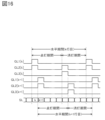
- FIG. 16 is a timing chart showing a method of driving the display device.
- 17A and 17B are diagrams showing configuration examples of a display device.
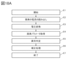
- 18A and 18B are diagrams showing an operation example of the display device.
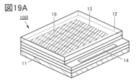
- 19A and 19B are diagrams showing configuration examples of a display device.
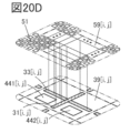
- 20A to 20D are diagrams showing configuration examples of display devices.
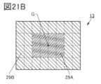
- 21A to 21C are diagrams showing configuration examples of display devices.
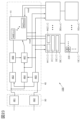
- FIG. 22 is a block diagram showing a configuration example of a display device.
- FIG. 23 is a block diagram showing a configuration example of a display device.
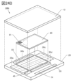
- 24A and 24B are diagrams showing configuration examples of a display device.
- FIG. 25 is a diagram illustrating a configuration example of a display device.
- FIG. 26 is a diagram illustrating a configuration example of a display device.
- 27A to 27C are diagrams showing configuration examples of display devices.
- 28A to 28F are diagrams showing configuration examples of pixels.
- 29A and 29B are diagrams showing configuration examples of a display device.
- FIG. 30 is a diagram illustrating a configuration example of a display device.
- FIG. 31 is a diagram illustrating a configuration example of a display device.
- FIG. 32 is a diagram illustrating a configuration example of a display device.
- FIG. 33 is a diagram illustrating a configuration example of a display device.
- FIG. 34 is a diagram illustrating a configuration example of a display device.
- FIG. 35 is a diagram illustrating a configuration example of a display device.
- FIG. 36 is a diagram illustrating a configuration example of a display device.
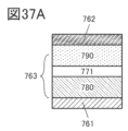
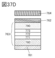
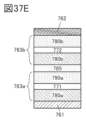
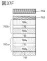
- 37A to 37F are diagrams showing configuration examples of light-emitting devices.
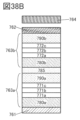
- 38A to 38C are diagrams showing configuration examples of light-emitting devices.
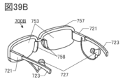
- 39A and 39B are diagrams illustrating examples of electronic devices.
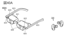
- 40A and 40B are diagrams illustrating examples of electronic devices.
- FIG. 41A is a diagram illustrating an example of an electronic device;
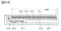
- FIG. 41B is a cross-sectional view showing an example of electronic equipment.
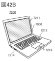
- 42A to 42D are diagrams showing examples of electronic devices.
- 43A to 43G are diagrams illustrating examples of electronic devices. 44A
- Electrically connected includes the case of being connected via "something that has some electrical action.”
- something having some kind of electrical action is not particularly limited as long as it enables transmission and reception of electrical signals between connection objects.
- the display system which is one embodiment of the present invention includes a first display device 1000A and a second display device 1002, and the first display device 1000A and the second display device.
- Each device 1002 has a communication function.
- the display system of one embodiment of the present invention may further have a third display device 1000B, or may have four or more display devices.
- 1 and 2 illustrate an example of a display system having a first display device 1000A, a second display device 1002, and a third display device 1000B.
- the communication function it is possible to have a communication function by wire connection, but it is preferable to have a communication function by radio (wireless communication function) because the usability of the display system can be improved.
- FIG. 1 is a diagram showing a one-on-one game competition using a display system according to one aspect of the present invention.
- One of the game players wears the first display device 1000A (spectacle-type display device or the like), and the third display device 1000B (spectacle-type display device or the like) is worn by the game player.
- the second display device 1002 (tablet-type display device or the like) is worn by the other player (second player) and placed in a position where it can be visually recognized by the first player and the second player. ing.
- the first player sees the display image 1040 of the second display device 1002 and the display image of the first display device 1000A (the image of the three-dimensional virtual object 1041 viewed from the position of the first display device 1000A). and both can be seen.
- the second player displays the display image 1040 of the second display device 1002 and the display image of the third display device 1000B (the image of the three-dimensional virtual object 1041 viewed from the position of the third display device 1000B).
- a third person for example, a spectator
- other than the players can visually recognize the display image 1040 on the second display device 1002 .
- the display image of the first display device 1000A and the display image of the third display device 1000B have images of the same three-dimensional virtual object 1041 viewed from different positions (viewpoints).
- the present invention is not limited to this, and the first display device 1000A and the third display device 1000B may display different images. Whether or not the display image of the first display device 1000A and the display image of the third display device 1000B display images of the same three-dimensional virtual object 1041 viewed from different positions (viewpoints). or can be arbitrarily set.
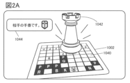
- FIG. 2A shows an example of the field of view of the first player wearing the first display device 1000A.
- the first player displays a display image 1042 (an image of the three-dimensional virtual object 1041 viewed from the position of the first display device 1000A) and a display image 1044 displayed by the first display device 1000A, and the first display device 1000A. and a display image 1040 of the second display device 1002 that is viewed through the .
- Display image 1044 is an example of an image displayed on first display device 1000A for the first player.
- the display position of the display image 1042 in FIG. 2A is preferably a position corresponding to the display position of the display image 1040 .
- a display image 1042 can be displayed at positions on the display image 1040 corresponding to the positions of the pieces moved by the first player and the second player.
- the first display device 1000A can display the display image 1042 superimposed on the transmission image (such as the display image 1040 of the second display device 1002).
- the transmitted image is an image transmitted through the display portion of the first display device 1000A when the display portion of the first display device 1000A is translucent (sometimes referred to as a see-through image). be able to.
- an imaging unit imaging means such as a camera or an image sensor
- an image a video see-through image captured by the imaging means of the first display device 1000A.
- the display system of one embodiment of the present invention has a function of acquiring position information of the first display device 1000A and the second display device 1002, and a display position of the display image 1042 based on the acquired position information. It is preferable to have a function to determine
- the display position of the display image 1042 can be determined so as to be a predetermined relative position to the display image 1040 that is visible through the display section of the first display device 1000A.
- the display position of the display image 1042 can be a position superimposed on the display image 1040 that is visible through the display unit of the first display device 1000A. Further, for example, the display position of the display image 1042 can be displayed at a position separated from the display image 1040 that is visible through the display section of the first display device 1000A.
- the display image 1042 on the first display device 1000A is displayed when at least part of the display portion of the second display device 1002 can be viewed as a transparent image, and when it cannot be viewed, the display image 1042 is displayed. An operation such as not displaying the image 1042 may be performed.
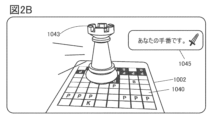
- FIG. 2B shows an example of the field of view of the second player wearing the third display device 1000B.
- the second player displays a display image 1043 (an image of the three-dimensional virtual object 1041 viewed from the position of the third display device 1000B) and a display image 1045 displayed by the third display device 1000B, and the third display device 1000B. and a display image 1040 of the second display device 1002 that is viewed through the .
- Display image 1045 is an example of an image displayed on third display device 1000B for the second player.
- the display position of the display image 1043 is preferably a position corresponding to the display position of the display image 1040 .
- a display image 1043 can be displayed at positions on the display image 1040 corresponding to the positions of the pieces moved by the first player and the second player.
- a third person (spectator) other than the player can visually recognize the display image 1040 of the second display device 1002 .
- part of information from the display system of one embodiment of the present invention can be obtained from the second display device 1002 even when the first display device 1000A and the third display device 1000B are not attached. .
- the first display on the first display device capable of AR display such as the glasses-type display device and the goggles-type display device
- the second display on the general display device such as the tablet-type display device.
- a new video experience can be realized by combining display of and display (which may be referred to as coordinated display, coordinated display, coordinated display, coordinated display, etc.).
- a first display device 1000 and a second display device 1002 included in the display system of one embodiment of the present invention are described with reference to FIGS. 3A and 3B.
- the display image of the first display device 1000 is displayed so as to correspond to the position of the second display device 1002 and the content of the display image. That is, the first display device 1000 has a function of acquiring position information of the first display device 1000 and the second display device 1002 .
- the display unit 1010 of the first display device 1000 has a function of displaying an image on the display unit according to the position of the display image of the second display device 1002 .
- the first display device 1000 includes a display unit 1010, a housing 1011, a sensor unit 1012, a communication unit 1013, a control unit 1014, a mounting unit 1016, and a display panel. 1017 and an optical member 1019 .
- the first display device 1000 may further include a camera section 1015 .
- the first display device 1000 and the second display device 1002 preferably have a storage unit.
- the first display device 1000 can project an image displayed on the display panel 1017 onto the display section 1010 of the optical member 1019 . Since the optical member 1019 has translucency, the user can see the image displayed in the display area superimposed on the transmitted image visually recognized through the optical member 1019 . Therefore, each of the first display devices 1000 is an electronic device capable of AR display.
- the second display device 1002 has a display unit 1020 , a housing 1021 , a sensor unit 1022 , a communication unit 1023 and a control unit 1024 .
- the second display device 1002 may further include a camera section 1025 .
- a distance measuring sensor capable of measuring the distance of an object
- the sensor unit 1012 can use an image sensor or a distance image sensor such as LIDAR (Light Detection and Ranging).
- LIDAR Light Detection and Ranging
- the sensor unit 1012 and the sensor unit 1022 preferably include an acceleration sensor such as a gyro sensor.
- an acceleration sensor such as a gyro sensor.
- wireless communication can be performed between the communication unit 1013 of the first display device 1000 and the communication unit 1023 of the second display device 1002.
- the communication unit has a wireless communication device, and can supply video signals, etc. by the wireless communication device.
- a connector to which a cable to which a video signal and a power supply potential are supplied may be provided.
- the first display device 1000 and the second display device 1002 can be paired using the communication section 1013 and the communication section 1023 .
- direct communication may be performed, or communication may be performed via a relay device.
- a wireless router such as Wi-Fi (registered trademark)
- an electronic device such as a smartphone
- an electronic device such as a PC (personal computer)
- a server connected via the Internet or the like can be used.
- the display image 1042 of the first display device 1000A (the image of the three-dimensional virtual object 1041 viewed from the position of the first display device 1000A) described with reference to FIGS.
- the display image 1042 of the first display device 1000A can be generated by the control unit 1024 of the second display device 1002.
- the first display device 1000 capable of AR display is a display device having a shape such as eyeglasses worn on the head, and the mounting space of the control unit 1014 and usable power are limited.
- the second display device 1002 (tablet or the like) having a large display area, a large mounting space for the control unit 1024 can be secured, and more power can be used compared to the control unit 1014 .
- the control unit 1024 preferably has a GPU (Graphics Processing Unit).
- the display unit 1010 of the first display device 1000 has a display function capable of recognizing a three-dimensional image with binocular vision (for example, if parallax is provided between the left and right display units), more dynamic image expression is possible. and is preferable.
- the housing 1011 may be provided with a touch sensor module.
- the touch sensor module has a function of detecting that the outer surface of housing 1011 is touched.
- the touch sensor module can detect a user's tap operation or slide operation and execute various processes. For example, it is possible to perform processing such as pausing or resuming a moving image by a tap operation, and fast-forward or fast-reverse processing can be performed by a slide operation. Further, by providing a touch sensor module for each of the two housings 1011, the range of operations can be expanded.
- Various touch sensors can be applied as the touch sensor module.
- various methods such as a capacitance method, a resistive film method, an infrared method, an electromagnetic induction method, a surface acoustic wave method, and an optical method can be adopted.
- a photoelectric conversion device (also referred to as a photoelectric conversion element) can be used as a light receiving device (also referred to as a light receiving element).
- a light receiving device also referred to as a light receiving element.
- an inorganic semiconductor and an organic semiconductor can be used for the active layer of the photoelectric conversion device.
- the first display device 1000 is provided with a battery, and can be charged wirelessly and/or wiredly.
- the first display device 1000 has a display unit 1010, a sensor unit 1012, a communication unit 1013, a control unit 1014, and a power supply unit 1018.
- the second display device 1002 has a display section 1020, a sensor section 1022, a communication section 1023, a control section 1024, and a power supply section 1028.
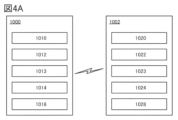
- FIGS. 3B and 4A illustrate configurations in which the first display device 1000 and the second display device 1002 have the same functions, but the present invention is not limited to this.
- the first display device 1000 and the second display device 1002 may have different functions.
- the first display device 1000 has a camera section 1015 and a headphone section 1110 in addition to the configuration shown in FIG. 4A.
- the second display device 1002 has a camera section 1025 and a second communication section 1029 in addition to the configuration shown in FIG. 4A.
- the camera unit 1015 may have an imaging unit such as an image sensor. Also, a plurality of cameras may be provided so as to be able to deal with a plurality of angles of view such as telephoto and wide angle.
- the second communication unit 1029 may have a function of performing communication with a function different from that of the communication unit 1023 .
- the communication unit 1023 has a function of communicating with the communication unit 1013, and the second communication unit 1029 supports the third generation mobile communication system (3G), the fourth generation mobile communication system (4G), the fifth It is only necessary to have a function that enables voice communication using a next-generation mobile communication system (5G) or a communication means that enables electronic payment.
- 3G third generation mobile communication system
- 4G fourth generation mobile communication system
- 5G next-generation mobile communication system
- FIG. 3 and FIG. 4 illustrate the communication between the first display device 1000 and the second display device 1002, the communication is not limited to this.
- the display system may further include a third display device 1000 (1000B). Also, the display system may have more display devices.
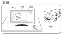
- FIG. 6A is a schematic diagram showing the field of view of the first display device 1000 (such as a glasses-type display device), similar to FIGS. 2A and 2B.
- the first display device 1000 such as a glasses-type display device
- the wearer of the first display device 1000 can visually recognize the display image 1060 displayed on the second display device 1002 through the display unit of the first display device 1000, and the display image 1061 can be seen. , is displayed at a position superimposed on the display image 1060 .
- FIG. 6A shows an example in which a display device that can be folded along the dashed line is used as the second display device 1002 . It is preferable to use a foldable display device as the second display device 1002 because space can be saved and storability and convenience are excellent.
- the display system of one embodiment of the present invention is not limited to this example.
- the communication unit of the first display device 1000 or the second display device 1002 has a communication function such as the Internet as described later, a player at a remote location (a player who is not at the same place) ) can be played against each other.
- a player at a remote location a player who is not at the same place
- each of the players who are not in the same place has the first display device 1000 and the second display device 1002, so that each of the players who are not in the same place can have a realistic video experience. and enjoy the gaming experience.
- the communication between display devices that are not located at the same location may be direct communication between the devices, or communication may be performed via a separately provided server.
- the application of the display system according to one aspect of the present invention is not limited to the amusement use described above.
- a two-dimensional drawing (display image 1060) is displayed on the second display device 1002.
- the first display device 1000 displays a 3D image (display image 1061) corresponding to the two-dimensional drawing.
- the display image 1061 may be displayed at a position not superimposed on the display image 1060, as shown in FIG. 6B. This allows designing while confirming the 3D image.
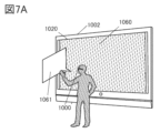
- FIGS. 7A and 7B a display system in which a first display device 1000 (such as a glasses-type display device) and a second display device 1002 used as digital signage can operate in cooperation may be used.
- FIG. 7A shows a first display device 1000 (such as a glasses type display device) and a second display device 1002 used as a planar digital signage.
- the first display device 1000 displays a display image 1061 related to part of the content displayed by the display image 1060 of the second display device 1002 .
- FIG. 7B shows a first display device 1000 (such as a glasses-type display device) and a second display device 1002 used as curved digital signage.
- the first display device 1000 displays a display image 1061 related to part of the content displayed by the display image 1060 of the second display device 1002 .
- the number of wearers of the first display device 1000 may be two or more.
- the owner can display the first display device 1000 owned privately and the public second display device 1002 (owned by a facility or the like) in cooperation with each other. It is also possible to link different display devices.
- FIGS. 1 to 7 each configuration of the display device and the display system of one embodiment of the present invention illustrated in FIGS. 1 to 7 is described below.
- the display portions 1010 and 1020 and the display panel 1017 each have a display function.
- the display unit 1010, the display unit 1020, and the display panel 1017 for example, one or more selected from a liquid crystal display device, a light emitting device including an organic EL, and a light emitting device including a light emitting diode such as a micro LED is used. can be used. In consideration of productivity and luminous efficiency, it is preferable to use light-emitting devices including organic EL for the display portions 1010 and 1020 and the display panel 1017 .
- the sensor unit 1012 and the sensor unit 1022 have a function of acquiring information related to the positional table of the first display device 1000 and the second display device 1002, respectively. More specifically, the sensor unit 1022 detects force, displacement, position, speed, acceleration, angular velocity, number of revolutions, distance, light, magnetism, temperature, sound, time, electric field, current, voltage, power, radiation, humidity, It has a function of measuring any one or more of inclination, vibration, smell, and infrared rays.
- the sensor unit 1012 and the sensor unit 1022 may have a function of detecting the line of sight of the user using data obtained by the above functions (for example, imaging data such as light).
- detection can be performed by, for example, a Pupil Center Corneal Reflection (PCCR) method or a Bright/Dark Pupil Effect method.
- PCCR Pupil Center Corneal Reflection
- the sensor unit 1012 preferably has a function of measuring electroencephalograms.
- it may have a plurality of electrodes that contact the head and have a mechanism for measuring electroencephalograms from weak currents flowing through the electrodes. Since the sensor portion 1012 has a function of measuring electroencephalograms, the user can operate the first display device 1000 and/or the second display device 1002 according to his/her thoughts. In this case, since the user does not need to use both hands to operate the display device, the user can perform input operations and the like without holding anything in both hands (both hands are free).
- the communication units 1013 and 1023 each have a function of wireless or wired communication. If the communication units 1013 and 1023 have a function of communicating wirelessly, it is preferable because the number of components such as cables for connection can be omitted.
- the communication units 1013 and 1023 can communicate via an antenna.
- communication means communication method between the communication unit 1013 and the communication unit 1023
- the Internet which is the foundation of the World Wide Web (WWW), intranet, extranet, PAN (Personal Area Network), LAN (Local Area Network) ), CAN (Campus Area Network), MAN (Metropolitan Area Network), WAN (Wide Area Network), GAN (Global Area Network), and other computer networks to communicate with each other.
- WWW World Wide Web
- intranet intranet
- extranet extranet
- PAN Personal Area Network
- LAN Local Area Network
- CAN Campus Area Network
- MAN Micropolitan Area Network
- WAN Wide Area Network
- GAN Global Area Network
- LTE Long Term Evolution
- GSM Global System for Mobile Communication: registered trademark
- EDGE Enhanced Data Rates for GSM Evolution
- CDMA2000 Code Divis ion Multiple Access 2000
- W-CDMA registered trademark
- IEEE specifications standardized by IEEE such as Wi-Fi (registered trademark), Bluetooth (registered trademark), and ZigBee (registered trademark).
- the control unit 1014 and the control unit 1024 each have a function of controlling the display unit.
- the control unit 1014 and the control unit 1024 include, for example, pixel circuits, backup circuits, image conversion circuits, and the like.
- the image conversion circuit can perform 3D image data construction processing, conversion processing from 3D image data to 2D image data, image data up-conversion processing, or down-conversion processing.
- the control unit 1014 and the control unit 1024 perform various data processing and program control by interpreting and executing instructions from various programs by the processor.
- a program that can be executed by a processor may be stored in a memory area of the processor, or may be stored in a storage unit.
- control unit 1014 and the control unit 1024 in addition to the CPU, other microprocessors such as a DSP (Digital Signal Processor) and GPU can be used singly or in combination. Also, these microprocessors may be realized by PLD (Programmable Logic Device) such as FPGA (Field Programmable Gate Array) or FPAA (Field Programmable Analog Array).
- PLD Programmable Logic Device
- FPGA Field Programmable Gate Array
- FPAA Field Programmable Analog Array
- the control unit 1014 and the control unit 1024 may have main memory.
- the main memory can comprise volatile memory such as RAM (Random Access Memory) or non-volatile memory such as ROM (Read Only Memory).
- a DRAM Dynamic Random Access Memory
- a virtual memory space is allocated and used as a work space for the control unit 1014 and the control unit 1024.
- the operating system, application programs, program modules, program data, etc. stored in the storage unit are loaded into RAM for execution. These data, programs, program modules, etc. loaded into the RAM are directly accessed and operated by the control unit 1014 and the control unit 1024 .
- ROM can store BIOS (Basic Input/Output System) that does not require rewriting, firmware, and so on.
- BIOS Basic Input/Output System
- mask ROM As the ROM, mask ROM, OTPROM (One Time Programmable Read Only Memory), EPROM (Erasable Programmable Read Only Memory), or the like can be used.
- EPROM include UV-EPROM (Ultra-Violet Erasable Programmable Read Only Memory), EEPROM (Electrically Erasable Programmable Read Only Memory), flash memory, etc., in which stored data can be erased by ultraviolet irradiation.
- control unit 1014 and the control unit 1024 have a processor specialized for parallel computation rather than a CPU.
- a processor having a large number of processor cores capable of parallel processing (for example, several tens to several hundred) such as GPU, TPU (Tensor Processing Unit), NPU (Neural Processing Unit).
- the control unit 1014 and the control unit 1024 can perform computations particularly related to the neural network at high speed.
- a flash memory for example, a flash memory, MRAM (Magnetoresistive Random Access Memory), PRAM (Phase change RAM), ReRAM (Resistive RAM), FeRAM (Ferroelectric RAM) or other non-volatile storage device is applied storage device, Alternatively, a memory device or the like to which a volatile memory element such as DRAM (Dynamic RAM) or SRAM (Static RAM) is applied may be used. Alternatively, a recording media drive such as a hard disk drive (HDD) or a solid state drive (SSD) may be used.
- HDD hard disk drive
- SSD solid state drive
- the power supply unit 1018 and the power supply unit 1028 each have a function of supplying power to the display unit.
- a primary battery or a secondary battery can be used for the power supply unit 1018 and the power supply unit 1028, for example.
- a lithium ion secondary battery can be used suitably, for example.
- FIG. 8 An example of an operation method of the display system of one embodiment of the present invention will be described with reference to FIGS. 8 and 9.
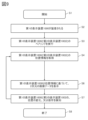
- FIG. 8 is a flow chart of a method of operating the display system.
- step S1 the operation is started. At this time, it is assumed that the first display device 1000 is in an activated state (operable state) and the second display device 1002 is in a power-on state.
- step S2 the first display device 1000 is attached.
- the first display device 1000 recognizes that it is attached, and the system starts up.
- step S2 for example, when the first display device 1000 is in the form of glasses, the image of the front camera may be provided to the user, or the image of other content may be displayed.
- step S3 pairing between the first display device 1000 and the second display device 1002 is performed.
- data can be exchanged bidirectionally between the first display device 1000 and the second display device 1002 .
- step S4 the first display device 1000 acquires the position information of the first display device 1000 and the second display device 1002.
- step S5 two-dimensional image data (for example, the display image 1042 shown in FIG. 2A) of the three-dimensional virtual object (for example, the three-dimensional virtual object 1041 shown in FIG. 1) viewed from the first display device 1000 is generated. .
- step S6 the image data generated in step S5 is displayed on the display unit 1010 of the first display device 1000 based on the position information.
- step S7 when the sensor unit included in the first display device 1000 or the second display device 1002 detects that the position of the first display device 1000 or the second display device 1002 has changed, in step S4 Move on to processing.
- step S4 Move on to processing.
- the process proceeds to step S4 in order to perform processing according to the operation.
- step S8 the process ends.
- step S8 for example, the first display device 1000 is removed, the first display device 1000 or the second display device 1002 is turned off, or the first display device 1000 and the second display device are turned off.
- the pairing with 1002 is canceled.
- step S5 shows the step of generating two-dimensional image data of the three-dimensional virtual object viewed from the first display device 1000, but step S5 does not necessarily have to be performed.
- the operation method of the display system without step S5 may be used.
- the first display device 1000 capable of AR display is described as a display device having a shape such as eyeglasses worn on the head, but is not necessarily limited to this shape. Even a display device that is not worn on the head, such as a smartphone or a tablet, can be used as the first display device 1000 if it has imaging means (a camera, an image sensor, or the like) and is capable of AR display. .
- imaging means a camera, an image sensor, or the like
- a display device with a new configuration or a display system with a new configuration can be provided. Further, by using the display device and the display system of one embodiment of the present invention, a method for operating a display device with a new structure or a method for operating a display system with a new structure can be provided. By using the display device and the display system of one embodiment of the present invention, realistic display and various expressions can be achieved.
- Embodiment 2 Structural examples of display devices that can be applied to the display devices of the electronic devices described in Embodiment 1 are described below with reference to drawings.
- FIG. 10A is a perspective view of a display device 10A that can be applied to the display device of the electronic device illustrated in Embodiment 1.
- FIG. The display device 10A can be applied to the first display device 1000 and the second display device 1002.
- FIG. 10A is a perspective view of a display device 10A that can be applied to the display device of the electronic device illustrated in Embodiment 1.
- FIG. 10A can be applied to the first display device 1000 and the second display device 1002.
- FIG. 10A is a perspective view of a display device 10A that can be applied to the display device of the electronic device illustrated in Embodiment 1.
- FIG. The display device 10A can be applied to the first display device 1000 and the second display device 1002.
- FIG. 10A is a perspective view of a display device 10A that can be applied to the display device of the electronic device illustrated in Embodiment 1.
- FIG. 10A can be applied to the first display device 1000 and the second display device 1002.
- the display device 10A has substrates 11 and 12 .
- the display device 10A has a display section 13 composed of elements provided between substrates 11 and 12 .
- the display unit 13 is an area for displaying an image in the display device 10A.
- the display section 13 has a plurality of pixels 230 .
- Pixel 230 has pixel circuit 51 and light emitting element 61 .
- the display unit 13 capable of displaying at a resolution of so-called full high-definition (also referred to as “2K resolution”, “2K1K”, or “2K”) is realized. can. Further, for example, when the pixels 230 are arranged in a matrix of 3840 ⁇ 2160 pixels, the display unit 13 can display at a resolution of so-called ultra high definition (also called “4K resolution”, “4K2K”, or “4K”). can be realized.
- the display unit 13 can display at a resolution of so-called Super Hi-Vision (also called “8K resolution”, “8K4K”, or “8K”). can be realized.
- Super Hi-Vision also called “8K resolution”, “8K4K”, or “8K”.
- the pixel density (definition) of the display unit 13 is preferably 1000 ppi or more and 10000 ppi or less. For example, it may be 2000 ppi or more and 6000 ppi or less, or 3000 ppi or more and 5000 ppi or less.
- the screen ratio (aspect ratio) of the display unit 13 is not particularly limited.
- the display unit 13 can correspond to various screen ratios such as 1:1 (square), 4:3, 16:9, and 16:10.
- a display element may be replaced with “device”.
- a display element, a light-emitting element, and a liquid crystal element can be called a display device, a light-emitting device, and a liquid crystal device.
- the display device 10A receives various signals and a power supply potential from the outside via the terminal section 14, and can perform image display using the display element provided in the display section 13.
- Various elements can be used as the display element.
- a light-emitting element having a function of emitting light such as an organic EL element and an LED element, a liquid crystal element, or a MEMS (Micro Electro Mechanical Systems) element can be applied.
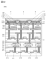
- a plurality of layers are provided between the substrate 11 and the substrate 12, and each layer is provided with a transistor for circuit operation or a display element for emitting light.
- a pixel circuit having a function of controlling operation of a display element a driver circuit having a function of controlling the pixel circuit, a functional circuit having a function of controlling the driver circuit, and the like are provided.
- FIG. 10B shows a perspective view schematically showing the configuration of each layer provided between the substrate 11 and the substrate 12. As shown in FIG. 10B
- a layer 20 is provided on the substrate 11 .
- Layer 20 has drive circuitry 30 , functional circuitry 40 and input/output circuitry 80 .
- Layer 20 has a transistor 21 (also called a Si transistor) with silicon in a channel forming region 22 .
- the substrate 11 is, for example, a silicon substrate.
- a silicon substrate is preferable because it has higher thermal conductivity than a glass substrate.
- the transistor 21 can be, for example, a transistor including single crystal silicon in a channel formation region (also referred to as a "c-Si transistor").
- a transistor including single crystal silicon in a channel formation region also referred to as a "c-Si transistor"
- the on current of the transistor can be increased. Therefore, the circuit included in the layer 20 can be driven at high speed, which is preferable.
- the Si transistor can be formed by microfabrication such that the channel length is 3 nm or more and 10 nm or less
- the display device 10A in which accelerators such as CPUs and GPUs, application processors, and the like are provided integrally with the display portion can be provided. .
- the layer 20 may be provided with a transistor having polycrystalline silicon in a channel formation region (also referred to as a "poly-Si transistor”).
- a transistor having polycrystalline silicon in a channel formation region also referred to as a "poly-Si transistor”
- polycrystalline silicon low temperature poly silicon (LTPS) may be used.
- LTPS transistor a transistor including LTPS in a channel formation region
- OS transistor may be provided in the layer 20 .
- the drive circuit 30 has, for example, a gate driver circuit, a source driver circuit, and the like.
- an arithmetic circuit, a memory circuit, a power supply circuit, and the like may be provided. Since the gate driver circuit, the source driver circuit, and other circuits can be arranged so as to overlap the display unit 13, the display device 10A can be arranged as compared with the case where these circuits and the display unit 13 are arranged side by side.
- the width of the non-display area (also referred to as a picture frame) existing on the periphery of the display section 13 can be made extremely narrow, and the size reduction of the display device 10A can be realized.
- the functional circuit 40 has, for example, the function of an application processor for controlling each circuit in the display device 10A and generating signals for controlling each circuit.
- the functional circuit 40 may also have a circuit for correcting image data, such as a GPU, and a CPU.
- the functional circuit 40 also includes an LVDS (Low Voltage Differential Signaling) circuit, a MIPI (Mobile Industry Processor Interface) circuit, and a D/A (Digital to Analog) conversion circuit or the like.
- the functional circuit 40 may also include a circuit for compressing and decompressing image data, a power supply circuit, and the like.
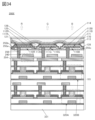
- a layer 50 is provided on the layer 20 .
- Layer 50 has pixel circuits 55 that include a plurality of pixel circuits 51 .
- Layer 50 may have transistor 52 with metal oxide in channel forming region 54 .
- the layer 50 may be provided with an OS transistor.
- the pixel circuit 51 may include an OS transistor. Note that the layer 50 can be provided by laminating on the layer 20 .
- a Si transistor may be provided in the layer 50 .
- the pixel circuit 51 may include a transistor having monocrystalline silicon or polycrystalline silicon in the channel formation region.
- LTPS may be used as the polycrystalline silicon.
- the pixel circuit 51 may be composed of a plurality of types of transistors using different semiconductor materials.
- the transistors may be provided in different layers for each type of transistor.
- the Si transistor and the OS transistor may be overlapped. By overlapping the transistors, the area occupied by the pixel circuit 51 can be reduced. Therefore, the definition of the display device 10A can be improved.
- a structure in which an LTPS transistor and an OS transistor are combined is sometimes called an LTPO.
- the transistor 52 which is an OS transistor
- a transistor having an oxide containing at least one of indium, element M (element M is aluminum, gallium, yttrium, or tin), and zinc in a channel formation region is preferably used.
- Such an OS transistor has a very low off-state current. Therefore, it is particularly preferable to use an OS transistor as a transistor provided in the pixel circuit because analog data written to the pixel circuit can be held for a long time.
- a layer 60 is provided on the layer 50 .
- a substrate 12 is provided on the layer 60 .
- the substrate 12 is preferably a translucent substrate or a layer made of a translucent material.
- Layer 60 is provided with a plurality of light emitting elements 61 .
- the layer 60 can be configured to be laminated on the layer 50 .
- an organic electroluminescence element also referred to as an organic EL element
- the light emitting element 61 is not limited to this, and may be an inorganic EL element made of an inorganic material, for example.
- the "organic EL element” and the "inorganic EL element” may be collectively referred to as the "EL element”.
- the light emitting element 61 may have inorganic compounds such as quantum dots. For example, by using quantum dots in the light-emitting layer, it can function as a light-emitting material.
- a display device 10A of one embodiment of the present invention can have a structure in which a light-emitting element 61, a pixel circuit 51, a driver circuit 30, and a functional circuit 40 are stacked; ratio (effective display area ratio) can be extremely high.
- the pixel aperture ratio can be 40% or more and less than 100%, preferably 50% or more and 95% or less, and more preferably 60% or more and 95% or less.
- the pixel circuits 51 can be arranged at an extremely high density, and the definition of the pixels can be made extremely high.
- Pixels can be arranged with a resolution of 20000 ppi or less, or 30000 ppi or less.
- Such a display device 10A has extremely high definition, it can be suitably used for devices for VR such as head-mounted displays, or glasses-type devices for AR. For example, even in the case of a configuration in which the display portion of the display device 10A is viewed through an optical member such as a lens, the display device 10A has an extremely high-definition display portion. A highly immersive display can be performed without being visually recognized.
- the diagonal size of the display unit 13 is 0.1 inch or more and 5.0 inches or less, preferably 0.5 inch or more and 2.0 inches or more. It can be 1 inch or less, more preferably 1 inch or more and 1.7 inch or less. For example, the diagonal size of the display unit 13 may be 1.5 inches or around 1.5 inches. By setting the diagonal size of the display unit 13 to 2.0 inches or less, it is possible to perform processing in one exposure process of an exposure device (typically a scanner device), thereby improving the productivity of the manufacturing process. can be improved.
- an exposure device typically a scanner device
- the display device 10A can be applied to devices other than wearable electronic devices.
- the diagonal size of the display portion 13 may exceed 2.0 inches.
- the configuration of the transistors used in the pixel circuit 51 may be appropriately selected according to the diagonal size of the display section 13 .
- the diagonal size of the display section 13 is preferably 0.1 inch or more and 3 inches or less.
- the diagonal size of the display section 13 is preferably 0.1 inch or more and 30 inches or less, more preferably 1 inch or more and 30 inches or less.
- the diagonal size of the display section 13 is preferably 0.1 inch or more and 50 inches or less, more preferably 1 inch or more and 50 inches or less.
- the diagonal size of the display section 13 is preferably 0.1 inch or more and 200 inches or less, more preferably 50 inches or more and 100 inches or less.
- the OS transistor is free from restrictions on the use of a laser crystallization apparatus or the like in the manufacturing process, or can be manufactured at a relatively low process temperature (typically 450° C. or lower), and thus has a relatively large area. (Typically, it is possible to correspond to a display device having a diagonal size of 50 inches or more and 100 inches or less). In addition, for LTPO, it is possible to support a diagonal size (typically, 1 inch or more and 50 inches or less) between the case of using an LTPS transistor and the case of using an OS transistor.
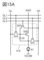
- FIG. 11 shows a pixel circuit 51, a driver circuit 30, and a functional circuit 40 included in the display device 10A, a plurality of wires connecting the pixel circuit 51, the driver circuit 30, and the functional circuit 40, and bus wires and the like in the display device 10A.
- FIG. 11 is a block diagram illustrating the .
- a plurality of pixel circuits 51 are arranged in a matrix on the layer 50.
- the drive circuit 30 has, as an example, a source driver circuit 31, a digital-to-analog converter (DAC) 32, an amplifier circuit 35, a gate driver circuit 33, and a level shifter .
- the functional circuit 40 has, as an example, a storage device 41 , a GPU (AI accelerator) 42 , an EL correction circuit 43 , a timing controller 44 , a CPU 45 , a sensor controller 46 and a power supply circuit 47 .
- the functional circuit 40 has the function of an application processor.
- the input/output circuit 80 is compatible with a transmission system such as LVDS (Low Voltage Differential Signaling). It has the function of distributing to The input/output circuit 80 also has a function of outputting information of the display device 10A to the outside via the terminal section 14 .
- LVDS Low Voltage Differential Signaling
- the circuit included in the drive circuit 30 and the circuit included in the function circuit 40 are each electrically connected to the bus line BSL.
- the source driver circuit 31 has a function of transmitting image data to the pixel circuit 51 included in the pixel 230 . Therefore, the source driver circuit 31 is electrically connected to the pixel circuit 51 via the wiring SL. A plurality of source driver circuits 31 may be provided.
- the digital-to-analog conversion circuit 32 has a function of converting image data digitally processed by a later-described GPU, correction circuit, etc. into analog data.
- the image data converted into analog data is amplified by an amplifier circuit 35 such as an operational amplifier and transmitted to the pixel circuit 51 via the source driver circuit 31 .
- the image data may be transmitted to the source driver circuit 31, the digital-analog conversion circuit 32, and the pixel circuit 51 in this order.
- the digital-to-analog converter circuit 32 and the amplifier circuit 35 may be included in the source driver circuit 31 .
- the gate driver circuit 33 has a function of selecting a pixel circuit to which image data is to be sent in the pixel circuit 51 . Therefore, the gate driver circuit 33 is electrically connected to the pixel circuit 51 via the wiring GL.
- a plurality of gate driver circuits 33 may be provided corresponding to the source driver circuits 31 .
- the level shifter 34 has a function of converting signals input to the source driver circuit 31, the digital-to-analog conversion circuit 32, the gate driver circuit 33, etc. to appropriate levels.
- the storage device 41 has a function of storing image data to be displayed on the pixel circuit 51 .
- the storage device 41 can be configured to store the image data as digital data or analog data.
- the storage device 41 when storing image data in the storage device 41, it is preferable that the storage device 41 be a non-volatile memory. In this case, for example, a NAND memory or the like can be applied as the storage device 41 .
- the storage device 41 when storing temporary data generated by the GPU 42, the EL correction circuit 43, the CPU 45, etc. in the storage device 41, it is preferable that the storage device 41 be a volatile memory.
- the storage device 41 for example, SRAM (Static Random Access Memory), DRAM (Dynamic Random Access Memory), etc. can be applied.
- the GPU 42 has, for example, a function of performing processing for outputting image data read from the storage device 41 to the pixel circuit 51 .
- the GPU 42 is configured to perform pipeline processing in parallel, the image data to be output to the pixel circuit 51 can be processed at high speed.
- GPU 42 can also function as a decoder for restoring encoded images.
- the functional circuit 40 may include a plurality of circuits that can improve the display quality of the display device 10A.
- a correction circuit color toning, dimming
- the functional circuit 40 may be provided with an EL correction circuit for correcting image data according to the characteristics of the light-emitting device.
- the functional circuit 40 includes an EL correction circuit 43 as an example.
- Artificial intelligence may also be used for the image correction described above.
- the current (or voltage applied to the pixel circuit) is monitored and acquired, the displayed image is acquired by an image sensor, etc., and the current (or voltage) and image are calculated by artificial intelligence (for example, , an artificial neural network, etc.), and the output result may be used to determine whether or not to correct the image.
- artificial intelligence for example, , an artificial neural network, etc.
- artificial intelligence calculations can be applied not only to image correction, but also to up-conversion processing to increase the resolution of image data.
- the GPU 42 in FIG. 11 illustrates blocks for performing various correction calculations (color unevenness correction 42a, up-conversion 42b, etc.).
- Algorithms for up-converting image data include the Nearest neighbor method, Bilinear method, Bicubic method, RAISR (Rapid and Accurate Image Super-Resolution) method, ANR (Anchored Neighborhood Regression) method, A+ method, SRCNN (Super -Resolution (Convolutional Neural Network) method or the like can be selected.
- the up-conversion process may be configured such that the algorithm used for the up-conversion process is changed for each region determined according to the gaze point. For example, the up-conversion processing of the gaze point and the area near the gaze point is performed with a slow but high-precision algorithm, and the up-conversion processing of areas other than the subject area is performed with a fast but low-accuracy algorithm. Just do it. With this configuration, the time required for up-conversion processing can be shortened. Also, the power consumption required for up-conversion processing can be reduced.
- up-conversion processing not only up-conversion processing, but also down-conversion processing that lowers the resolution of image data may be performed. If the resolution of the image data is higher than the resolution of the display section 13 , part of the image data may not be displayed on the display section 13 . In such a case, the entire image data can be displayed on the display unit 13 by performing down-conversion processing.
- the timing controller 44 has a function of controlling the drive frequency (frame frequency, frame rate, refresh rate, etc.) for displaying images. For example, when displaying a still image on the display device 10A, the power consumption of the display device 10A can be reduced by lowering the drive frequency by the timing controller 44 .
- the CPU 45 has a function of performing general-purpose processing such as, for example, operating system execution, data control, various calculations, and program execution.
- the CPU 45 has a role of issuing commands such as, for example, an image data write operation or read operation in the storage device 41, an image data correction operation, and an operation to a sensor, which will be described later.
- the CPU 45 may have a function of transmitting a control signal to at least one of the circuits included in the functional circuit 40 .
- the sensor controller 46 has a function of controlling sensors.
- a wiring SNCL is illustrated as a wiring for electrically connecting to the sensor.
- a touch sensor that can be provided in the display unit 13 can be used as the sensor.
- the sensor may be, for example, an illuminance sensor.
- the power supply circuit 47 has a function of generating a voltage to be supplied to the pixel circuit 51, the drive circuit 30, the functional circuit 40, and the like.
- the power supply circuit 47 may have a function of selecting a circuit to supply voltage.
- the power supply circuit 47 can reduce the power consumption of the entire display device 10A by stopping voltage supply to the CPU 45, GPU 42, etc. during the period in which a still image is displayed.
- the display device of one embodiment of the present invention can have a structure in which the display element, the pixel circuit, and the driver circuit and function circuit 40 are stacked.
- a driver circuit and a functional circuit which are peripheral circuits, can be arranged so as to overlap with the pixel circuit, and the width of the frame can be extremely narrowed, so that the display device can be miniaturized.
- the display device of one embodiment of the present invention has a structure in which circuits are stacked, the wiring that connects the circuits can be shortened; thus, the display device can be lightweight. .
- the display device of one embodiment of the present invention can include a display portion with improved pixel definition, the display device can have excellent display quality.
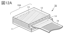
- FIG. 12A to 12C are perspective views of the display module 70.
- FIG. A display module 70 shown in FIG. 12A has a structure in which an FPC 74 (FPC: flexible printed circuit) is provided in the terminal section 14 of the display device 10A.
- the FPC 74 has a structure in which a film made of an insulator is provided with wiring. Also, the FPC 74 has flexibility.
- the FPC 74 functions as wiring for externally supplying video signals, control signals, power supply potential, and the like to the display device 10A.
- an IC may be mounted on the FPC 74 .
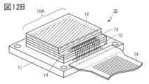
- a display module 70 shown in FIG. 12B has a configuration in which a display device 10A is provided on a printed wiring board 71.
- the printed wiring board 71 has a structure in which wiring is provided inside or on the surface of a substrate made of an insulator, or inside and on the surface.
- the terminal section 14 of the display device 10A and the terminal section 72 of the printed wiring board 71 are electrically connected via wires 73 .
- the wire 73 can be formed by wire bonding. Ball bonding or wedge bonding can be used as wire bonding.
- the wires 73 may be covered with a resin material or the like.
- the electrical connection between the display device 10A and the printed wiring board 71 may be made by a method other than wire bonding.
- the electrical connection between the display device 10A and the printed wiring board 71 may be realized by an anisotropic conductive adhesive, bumps, or the like.
- the terminal portion 72 of the printed wiring board 71 is electrically connected to the FPC 74 .
- the terminal portion 14 and the FPC 74 may be electrically connected via the printed wiring board 71 .
- the wiring formed on the printed wiring board 71 can be used to convert the spacing (pitch) between the electrodes of the terminal section 14 to the spacing of the electrodes of the terminal section 72 . That is, even when the pitch of the electrodes provided in the terminal section 14 and the pitch of the electrodes provided in the FPC 74 are different, the electrodes can be electrically connected.
- the printed wiring board 71 can be provided with various elements such as resistance elements, capacitive elements, and semiconductor elements.
- the terminal portion 72 is electrically connected to the connection portion 75 provided on the lower surface of the printed wiring board 71 (the surface on which the display device 10A is not provided). good too.
- the display module 70 can be easily attached to and detached from another device.
- FIG. 13A and 13B show a configuration example of the pixel circuit 51 and a light emitting element 61 connected to the pixel circuit 51.
- FIG. FIG. 13A is a diagram showing connection of each element
- FIG. 13B schematically shows a vertical relationship among a layer 20 including a driver circuit, a layer 50 including a plurality of transistors included in a pixel circuit 51, and a layer 60 including a light emitting element 61. It is a diagram.
- a pixel circuit 51 shown as an example in FIGS. 13A and 13B includes a transistor 52A, a transistor 52B, a transistor 52C, and a capacitor 53.
- FIG. The transistors 52A, 52B, and 52C can be OS transistors.
- Each of the transistor 52A, transistor 52B, and transistor 52C preferably has a back gate electrode. can be configured.
- the transistor 52B includes a gate electrode electrically connected to the transistor 52A, a first terminal electrically connected to the light emitting element 61, and a second terminal electrically connected to the wiring ANO.
- the wiring ANO is wiring for applying a potential for supplying current to the light emitting element 61 .
- the transistor 52A has a first terminal electrically connected to the gate electrode of the transistor 52B, a second terminal electrically connected to a wiring SL functioning as a source line, and a wiring GL1 functioning as a gate line. and a gate electrode having a function of controlling a conducting state or a non-conducting state based on the potential.
- the transistor 52C is turned on based on the potentials of the first terminal electrically connected to the wiring V0, the second terminal electrically connected to the light emitting element 61, and the wiring GL2 functioning as a gate line. or a gate electrode having a function of controlling a non-conducting state.
- the wiring V0 is a wiring for applying a reference potential and a wiring for outputting the current flowing through the pixel circuit 51 to the driving circuit 30 or the function circuit 40 .
- the capacitor 53 includes a first conductive film electrically connected to the gate electrode of the transistor 52B and a second conductive film electrically connected to the second terminal of the transistor 52C.
- the light emitting element 61 includes a first electrode electrically connected to the first terminal of the transistor 52B and a second electrode electrically connected to the wiring VCOM.
- the wiring VCOM is a wiring for applying a potential for supplying current to the light emitting element 61 .
- the intensity of light emitted by the light emitting element 61 can be controlled according to the image signal applied to the gate electrode of the transistor 52B. Variation in the voltage between the gate and source of the transistor 52B can be suppressed by the reference potential of the wiring V0 applied through the transistor 52C.
- a current value that can be used to set pixel parameters can also be output from the wiring V0.
- the wiring V0 can function as a monitor line for outputting the current flowing through the transistor 52B or the current flowing through the light emitting element 61 to the outside.
- the current output to the wiring V0 is converted into a voltage by a source follower circuit or the like and output to the outside. Alternatively, it can be converted into a digital signal by an AD converter or the like and output to the functional circuit 40 or the like.
- the light-emitting element described in one embodiment of the present invention refers to a self-luminous display element such as an organic EL device (also referred to as an OLED (Organic Light Emitting Diode)).
- the light-emitting elements electrically connected to the pixel circuit can be self-luminous light-emitting elements such as LEDs (Light Emitting Diodes), micro LEDs, QLEDs (Quantum-dot Light Emitting Diodes), and semiconductor lasers. is.
- the wiring that electrically connects the pixel circuit 51 and the driving circuit 30 can be shortened, so that the wiring resistance of the wiring can be reduced. Therefore, since data can be written at high speed, the display device 10A can be driven at high speed. As a result, a sufficient frame period can be ensured even if the number of pixel circuits 51 included in the display device 10A is increased, so the pixel density of the display device 10A can be increased. Further, by increasing the pixel density of the display device 10A, the definition of the image displayed by the display device 10A can be increased.
- the pixel density of the display device 10A can be 1000 ppi or more, or 5000 ppi or more, or 7000 ppi or more. Therefore, the display device 10A can be a display device for AR or VR, for example, and can be suitably applied to an electronic device such as an HMD in which the distance between the display unit and the user is short.
- FIGS. 13A and 13B show the pixel circuit 51 including a total of three transistors as an example, but one embodiment of the present invention is not limited to this.
- a configuration example of a pixel circuit and an example of a driving method applicable to the pixel circuit 51 will be described below.
- a pixel circuit 51A shown in FIG. 14A illustrates a transistor 52A, a transistor 52B, and a capacitor 53.
- FIG. 14A also shows the light emitting element 61 connected to the pixel circuit 51A.
- a wiring SL, a wiring GL, a wiring ANO, and a wiring VCOM are electrically connected to the pixel circuit 51A.
- the pixel circuit 51A has a configuration obtained by removing the transistor 52C from the pixel circuit 51 shown in FIG. 13A and replacing the wiring GL1 and the wiring GL2 with the wiring GL.
- the transistor 52A has a gate electrically connected to the wiring GL, one of the source and the drain electrically connected to the wiring SL, and the other electrically connected to the gate of the transistor 52B and one electrode of the capacitor C1.
- One of the source and drain of the transistor 52B is electrically connected to the wiring ANO and the other is electrically connected to the anode of the light emitting element 61 .
- the other electrode of the capacitor C1 is electrically connected to the anode of the light emitting element 61 .
- the cathode of the light emitting element 61 is electrically connected to the wiring VCOM.
- a pixel circuit 51B shown in FIG. 14B has a configuration in which a transistor 52C is added to the pixel circuit 51A.
- a wiring V0 is electrically connected to the pixel circuit 51B.
- a pixel circuit 51C shown in FIG. 14C is an example in which a pair of transistors with electrically connected gates is applied to the transistor 52A and the transistor 52B of the pixel circuit 51A.
- a pixel circuit 51D shown in FIG. 14D is an example in which the transistor is applied to the pixel circuit 51B. This can increase the current that the transistor can pass. Note that although a transistor having a pair of gates electrically connected to each other is used as all the transistors here, the present invention is not limited to this. Alternatively, a transistor having a pair of gates and electrically connected to different wirings may be used. For example, reliability can be improved by using a transistor in which one of the gates and the source are electrically connected.
- a pixel circuit 51E shown in FIG. 15A has a configuration in which a transistor 52D is added to the pixel circuit 51B.
- a wiring GL1, a wiring GL2, and a wiring GL3 functioning as gate lines are electrically connected to the pixel circuit 51E.
- the wiring GL1, the wiring GL2, and the wiring GL3 may be collectively referred to as the wiring GL. Therefore, the number of wirings GL is not limited to one, and may be plural.
- the transistor 52D has a gate electrically connected to the wiring GL3, one of the source and the drain electrically connected to the gate of the transistor 52B, and the other electrically connected to the wiring V0.
- a gate of the transistor 52A is electrically connected to the wiring GL1
- a gate of the transistor 52C is electrically connected to the wiring GL2.
- Such a pixel circuit is suitable for a display method in which display periods and off periods are alternately provided.
- a pixel circuit 51F shown in FIG. 15B is an example in which a capacitor 53A is added to the pixel circuit 51E.
- Capacitor 53A functions as a holding capacitor.
- a pixel circuit 51G shown in FIG. 15C and a pixel circuit 51H shown in FIG. 15D are examples in which a transistor having a pair of gates is applied to the pixel circuit 51E or the pixel circuit 51F, respectively.
- a transistor whose gates are electrically connected to each other is applied to the transistors 52A, 52C, and 52D, and a transistor whose one gate is electrically connected to its source is applied to the transistor 52B.
- FIG. 16 shows a timing chart relating to a method of driving a display device to which the pixel circuit 51E is applied.
- FIG. 16 shows timings of signals supplied to the wiring SL functioning as a source line.
- a high-level potential is applied to the wirings GL1[k] and GL2[k], and a source signal is applied to the wiring SL. Accordingly, the transistor 52A and the transistor 52C are brought into conduction, and a potential corresponding to the source signal is written from the wiring SL to the gate of the transistor 52B. After that, when a low-level potential is applied to the wirings GL1[k] and GL2[k], the transistors 52A and 52C are brought out of conduction, and the gate potential of the transistor 52B is held.
- a high-level potential is applied to the wiring GL2[k] and the wiring GL3[k] in the off period of the k-th row.
- the transistors 52C and 52D are brought into a conductive state, and the same potential is supplied to the source and gate of the transistor 52B, so that almost no current flows through the transistor 52B.
- the light emitting element 61 is extinguished. All pixels located in the k-th row are turned off. The pixels in the k-th row are kept off until the next lighting period.
- a driving method in which a light-off period is provided during one horizontal period instead of always lighting during one horizontal period can be called duty driving.
- duty driving an afterimage phenomenon when displaying moving images can be reduced, so that a display device with high moving image display performance can be realized.
- so-called VR motion sickness can be alleviated by reducing afterimages.
- the ratio of the lighting period to one horizontal period can be called the duty ratio.
- the duty ratio when the duty ratio is 50%, it means that the lighting period and the lighting-out period have the same length.
- the duty ratio can be freely set, and can be appropriately adjusted within a range of, for example, higher than 0% and 100% or less.
- FIGS. 17A and 17B A configuration different from the pixel circuit described above will be described with reference to FIGS. 17A and 17B.
- FIG. 17A A block diagram of the pixel 230 is shown in FIG. 17A.
- the pixel shown in FIG. 17A has a switching transistor (Switching Tr), a driving transistor (Driving Tr), a light-emitting element (LED), and a storage circuit MEM (Memory).
- switching Tr switching transistor
- driving Tr driving transistor
- LED light-emitting element
- MEM Storage circuit
- Data DataW is supplied to the memory circuit MEM via the wiring SL2 and the transistor 52A.
- the data DataW is supplied to the pixel in addition to the image data Data, the current flowing through the light emitting element increases, and the display device can display high luminance.
- FIG. 17B shows a specific circuit diagram of the pixel circuit 51I.
- a pixel circuit 51I shown in FIG. 17B has a transistor 52w, a transistor 52A, a transistor 52B, a transistor 52C, a capacitor 53s, and a capacitor 53w.
- FIG. 17B also illustrates the light emitting element 61 connected to the pixel circuit 51I.
- the transistor 52w functions as a switching transistor.
- Transistor 52B functions as a drive transistor.
- One of the source and drain of the transistor 52w is electrically connected to one electrode of the capacitor 53w.
- the other electrode of capacitor 53w is electrically connected to one of the source and drain of transistor 52A.
- One of the source or drain of transistor 52A is electrically connected to the gate of transistor 52B.
- a gate of the transistor 52B is electrically connected to one electrode of the capacitor 53s.
- the other electrode of the capacitor 53s is electrically connected to one of the source and drain of the transistor 52B.
- One of the source and drain of transistor 52B is electrically connected to one of the source and drain of transistor 52C.
- One of the source and drain of transistor 52C is electrically connected to one electrode of light emitting element 61 .
- Each transistor illustrated in FIG. 17B has a back gate electrically connected to the gate, but the connection of the back gate is not limited to this. In addition, the transistor need not have a back gate.
- the node to which the other electrode of the capacitor 53w, one of the source and drain of the transistor 52A, the gate of the transistor 52B, and one electrode of the capacitor 53s are connected is referred to as a node NM.
- a node to which the other electrode of the capacitor 53s, one of the source and drain of the transistor 52B, one of the source and drain of the transistor 52C, and one electrode of the light emitting element 61 are connected is a node NA.
- a gate of the transistor 52w is electrically connected to the wiring GL1.
- a gate of the transistor 52C is electrically connected to the wiring GL1.
- a gate of the transistor 52A is electrically connected to the wiring GL2.
- the other of the source and the drain of transistor 52w is electrically connected to line SL1.
- the other of the source and the drain of transistor 52C is electrically connected to line V0.
- the other of the source and the drain of transistor 52A is electrically connected to line SL2.
- the wiring SL1 and the wiring SL2 may be collectively referred to as the wiring SL. Therefore, the wiring SL is not limited to one, and may be plural.
- the other of the source and drain of the transistor 52B is electrically connected to the wiring ANO.
- the other electrode of light emitting element 61 is electrically connected to wiring VCOM.
- the wiring GL1 and the wiring GL2 can function as signal lines for controlling the operation of transistors.
- the wiring SL1 can function as a signal line that supplies image data Data to pixels.
- the wiring SL2 can function as a signal line for writing data DataW to the memory circuit MEM.
- the wiring SL2 can function as a signal line that supplies correction signals to pixels.
- the wiring V0 functions as a monitor line for obtaining electrical characteristics of the transistor 52B. Further, by supplying a specific potential from the wiring V0 to the other electrode of the capacitor 53s through the transistor 52C, writing of the image signal can be stabilized.
- the transistor 52A and the capacitor 53w constitute a memory circuit MEM.
- the node NM is a storage node, and by turning on the transistor 52A, data DataW supplied from the wiring SL2 can be written to the node NM.
- the potential of the node NM can be held for a long time.
- the image data Data supplied from the wiring SL1 is supplied to the capacitor 53w through the transistor 52w.
- One of the source or drain of transistor 52w and node NM are capacitively coupled. Therefore, the potential of the node NM to which the data DataW is written changes according to the image data Data.
- the node NA and the node NM are capacitively coupled via the capacitor 53s. Therefore, the potential of the node NA changes according to the data DataW and the image data Data.
- the transistor 52w functions as a selection transistor that determines whether or not to receive the supply of the image data Data.
- the transistor 52C functions as a reset transistor that determines whether the potential of the node NA is made equal to that of the wiring V0.
- the display device of one embodiment of the present invention can detect a defective pixel with the use of the functional circuit 40 provided so as to overlap with the pixel circuit group 55 .
- the display defect caused by the defective pixel can be corrected, and normal display can be performed.
- a part or all of the correction methods exemplified below may be executed by a circuit provided outside the display device. Also, part of the correction method may be performed by the functional circuit 40 and the other part may be performed by a circuit provided outside the display device.
- FIG. 18A is a flowchart for the correction method described below.
- step E1 the correction operation is started in step E1.
- step E2 the pixel current is read.
- each pixel can be driven to output current to a monitor line electrically connected to the pixel.
- the current reading operation can be performed simultaneously for each section 59. Since the pixel circuit group 55 is divided into a plurality of sections 59, it is possible to perform the readout operation of the current of all the pixels in an extremely short time.
- step E3 the read current is converted into voltage.
- a digital signal is to be handled in subsequent processing, it can be converted into digital data in step E3.
- ADC analog-to-digital conversion circuit
- Pixel parameters of each pixel are obtained based on the obtained data.
- Pixel parameters include, for example, the threshold voltage or field effect mobility of a driving transistor, the threshold voltage of a light emitting element, and the current value at a predetermined voltage.
- step E5 it is determined whether or not each pixel is abnormal based on the pixel parameters. For example, if the pixel parameter value exceeds (or falls below) a predetermined threshold value, the pixel is identified as an abnormal pixel.
- Abnormalities include dark point defects that are extremely low in luminance relative to the input data potential, and bright point defects that are extremely high in luminance.
- step E5 the address of the abnormal pixel and the type of defect can be identified and acquired.
- step E6 correction processing is performed.
- FIG. 18B schematically shows a pixel having a set of 3 ⁇ 3 pixel circuits 51 and light emitting elements 61 . Assume that the center pixel is pixel 151 with a dark spot defect. FIG. 18B schematically shows that the pixel 151 is turned off and the surrounding pixels 150 are turned on with a predetermined luminance.
- a dark spot defect is a defect in which the luminance of a pixel is unlikely to reach normal luminance even if correction is made to increase the data potential input to the pixel. Therefore, as shown in FIG. 18B, the pixels 150 surrounding the pixel 151 having the dark spot defect are corrected to increase the luminance. As a result, a normal image can be displayed even when a dark spot defect occurs.
- correction parameters can be set for each pixel.
- the correction parameters By applying the correction parameters to the input image data, it is possible to generate corrected image data for displaying an optimum image on the display device 10A.
- correction parameters can be set so as to cancel (level) variations in pixel parameters.
- a reference value is set based on the median value or average value of pixel parameters for some or all pixels, and the correction value for canceling the difference from the reference value for the pixel parameter of a predetermined pixel is It can be set as a correction parameter for the pixel.
- correction data that takes into account both the correction amount for compensating for the abnormal pixel and the correction amount for canceling variations in pixel parameters.
- step E7 the correction operation is terminated.
- images can be displayed based on the correction parameters acquired in the above correction operation and the input image data.
- a neural network may be used as one of the steps of the correction operation.
- correction parameters can be determined, for example, based on inference results obtained by machine learning. For example, when a neural network is used to determine correction parameters, highly accurate correction can be performed so that abnormal pixels are not conspicuous without using a detailed algorithm for correction.
- FIG. 19A and 19B show perspective views of a display device 10B that is a modification of the display device 10A.
- FIG. 19B is a perspective view for explaining the structure of each layer included in the display device 10B. In order to reduce the repetition of description, mainly the points different from the display device 10A will be described.
- a pixel circuit group 55 including a plurality of pixel circuits 51 and a driving circuit 30 are overlapped.
- the pixel circuit group 55 is divided into a plurality of divisions 59, and the driving circuit 30 is divided into a plurality of divisions 39.
- FIG. A plurality of partitions 39 each have a source driver circuit 31 and a gate driver circuit 33 .
- FIG. 20A shows a configuration example of the pixel circuit group 55 included in the display device 10B.
- FIG. 20B shows a configuration example of the drive circuit 30 included in the display device 10B.
- the partitions 59 and 39 are respectively arranged in a matrix of m rows and n columns (m and n are integers equal to or greater than 1).
- the partition 59 on the first row and the first column is indicated as partition 59[1,1]
- the partition 59 on the m-th row and n-th column is indicated as partition 59[m,n].
- the partition 39 in the first row and first column is indicated as partition 39[1,1]
- the partition 39 in the mth row and nth column is indicated as partition 39[m,n].
- 20A and 20B show the case where m is 4 and n is 8. FIG. That is, each of the pixel circuit group 55 and the driving circuit 30 is divided into 32 parts.
- Each of the plurality of partitions 59 has a plurality of pixel circuits 51, a plurality of wirings SL, and a plurality of wirings GL.
- one of the plurality of pixel circuits 51 is electrically connected to at least one of the plurality of wirings SL and at least one of the plurality of wirings GL.
- One of the divisions 59 and one of the divisions 39 are overlapped (see FIG. 20C).
- the section 59[i,j] (i is an integer of 1 or more and m or less and j is an integer of 1 or more and n or less) and the section 39[i,j] are overlapped.
- the source driver circuit 31[i,j] included in the section 39[i,j] is electrically connected to the wiring SL included in the section 59[i,j].
- the gate driver circuit 33[i,j] included in the section 39[i,j] is electrically connected to the wiring GL included in the section 59[i,j].
- the source driver circuit 31[i,j] and the gate driver circuit 33[i,j] have a function of controlling the plurality of pixel circuits 51 included in the section 59[i,j].
- the pixel circuits 51 included in the partitions 59[i,j] and the partitions 39[i,j] By overlapping the partitions 59[i,j] and the partitions 39[i,j], the pixel circuits 51 included in the partitions 59[i,j], the source driver circuits 31 included in the partitions 39[i,j], and the The connection distance (wiring length) with the gate driver circuit 33 can be extremely shortened. As a result, since wiring resistance and parasitic capacitance are reduced, the time required for charging and discharging is shortened, and high-speed driving can be realized. Also, power consumption can be reduced. In addition, miniaturization and weight reduction can be realized.
- the display device 10B has a configuration in which each section 39 has a source driver circuit 31 and a gate driver circuit 33 . Therefore, it is possible to divide the display unit 13 into sections 59 corresponding to the sections 39 and rewrite the image data. For example, it is possible to rewrite the image data only in the section of the display unit 13 where the image has changed, and to retain the image data in the section where the image has not changed, so that power consumption can be reduced.
- one of the display sections 13 divided into each section 59 is called a sub-display section 19 . Therefore, it can be said that the sub-display section 19 is divided into each section 39 .
- the display device 10B described with reference to FIGS. 19 and 20 shows the case where the display section 13 is divided into 32 sub-display sections 19 (see FIG. 19A).
- the sub display portion 19 includes a plurality of pixels 230 shown in FIG. 13 and the like.
- one sub-display portion 19 includes one of the sections 59 including a plurality of pixel circuits 51 and a plurality of light emitting elements 61 .
- one section 39 has a function of controlling a plurality of pixels 230 included in one sub-display section 19 .
- the display device 10B can arbitrarily set the drive frequency during image display for each sub-display section 19 by means of the timing controller 44 of the functional circuit 40 .
- the functional circuit 40 has the function of controlling the operation of each of the multiple compartments 39 and the multiple compartments 59 . That is, the functional circuit 40 has a function of controlling the drive frequency and operation timing of each of the plurality of sub-display sections 19 arranged in a matrix.
- the functional circuit 40 also has a function of adjusting synchronization between the sub-displays.
- a timing controller 441 and an input/output circuit 442 may be provided for each section 39 (see FIG. 20D).
- the input/output circuit 442 for example, an I2C (Inter-Integrated Circuit) interface or the like can be used.
- the timing controller 441 included in the section 39[i,j] is indicated as timing controller 441[i,j].
- the input/output circuit 442 included in the partition 39[i,j] is indicated as an input/output circuit 442[i,j].
- the function circuit 40 supplies the input/output circuit 442[i,j] with setting signals for the scanning direction and driving frequency of the gate driver circuit 33[i,j], and the number of pixels to be thinned out of the image data when the resolution is reduced. Operation parameters such as (the number of pixels not to be rewritten when rewriting image data) are supplied.
- the source driver circuits 31[i,j] and the gate driver circuits 33[i,j] operate according to the operation parameters.
- the input/output circuit 442 outputs information photoelectrically converted by the light receiving element to the function circuit 40 .
- the display device 10B in the electronic device of one embodiment of the present invention has low power consumption by stacking the pixel circuits 51 and the driver circuits 30 and varying the driving frequency of each sub-display portion 19 according to the movement of the user's line of sight. can be improved.
- FIG. 21A shows the display section 13 having the sub-display section 19 of 4 rows and 8 columns. Also, FIG. 21A shows a first region S1 to a third region S3 centering on the point of gaze G.
- the CPU 45 assigns each of the plurality of sub display portions 19 to either a first section 29A overlapping the first area S1 or the second area S2, or a second area 29B overlapping the third area S3. That is, the CPU 45 distributes each of the plurality of sections 39 to the first section 29A or the second section 29B.
- the first section 29A that overlaps the first area S1 or the second area S2 includes an area that overlaps the point of gaze G.
- the second section 29B includes the sub-display portion 19 located outside the first section 29A (see FIG. 21B).
- the function circuit 40 controls the operation of the drive circuits (the source driver circuits 31 and the gate driver circuits 33 ) of each of the plurality of partitions 39 .
- the second area 29B is an area that overlaps with the third area S3 including the above-described stable fixation field, guidance field, and auxiliary field of view, and is a field where the user's discriminating power is low. Therefore, even if the second area 29B is smaller than the first area 29A in the number of times the image data is rewritten per unit time (hereinafter also referred to as "the number of times of image rewriting") during image display, the user's perception of the image data is substantially reduced. display quality (hereinafter also referred to as “substantial display quality”) is less degraded.
- the drive frequency (also referred to as the “second drive frequency”) of the sub-display section 19 included in the second section 29B is changed to the drive frequency (also referred to as the “first drive frequency”) of the sub-display section 19 included in the first section 29A. ), there is little substantial deterioration in display quality.
- the power consumption of the display device can be reduced.
- lowering the drive frequency also lowers the display quality.
- the display quality during moving image display is degraded.
- by making the second drive frequency lower than the first drive frequency it is possible to reduce the power consumption in an area with low visibility for the user and to suppress the substantial deterioration of the display quality. .
- the first drive frequency should be 30 Hz or more and 500 Hz or less, preferably 60 Hz or more and 500 Hz or less.
- the second drive frequency is preferably equal to or less than the first drive frequency, more preferably equal to or less than 1/2 of the first drive frequency, and more preferably equal to or less than 1/5 of the first drive frequency.
- a region farther from the first region 29A is set as a third region 29C (see FIG. 21C), and the sub-display portions 19 included in the third region 29C are driven.
- the frequency (also referred to as "third drive frequency”) may be lower than that of the second section 29B.
- the third drive frequency is preferably equal to or less than the second drive frequency, more preferably equal to or less than 1/2 of the second drive frequency, and more preferably equal to or less than 1/5 of the second drive frequency. Power consumption can be further reduced by significantly reducing the number of times the image is rewritten. Also, rewriting of image data may be stopped as necessary. Power consumption can be further reduced by stopping rewriting of image data.
- a transistor having an extremely small off-state current As the transistor forming the pixel circuit 51 .
- an OS transistor As a transistor forming the pixel circuit 51 . Since the OS transistor has extremely low off current, it can hold image data supplied to the pixel circuit 51 for a long time.
- an OS transistor for the transistor 52A it is preferable to use an OS transistor for the transistor 52A.
- an image may be displayed that is significantly different in brightness, contrast, color tone, etc. from the previous image.
- there is a difference in the timing of image switching between the first area 29A and the area with a drive frequency lower than that of the first area 29A. etc. are greatly different, and the substantial display quality may be impaired.
- the image data in the areas other than the first area 29A are once rewritten with the same driving frequency as the first area 29A, and then the driving frequency of the areas other than the first area 29A is changed. should be lowered.
- the areas other than the first area 29A are also rewritten with the same driving frequency as the first area 29A, and the amount of change is within the certain amount. If it is determined that, the driving frequency of the zones other than the first zone 29A may be lowered. Also, when it is determined that the amount of change in the point of gaze G is small, the drive frequency for the zones other than the first zone 29A may be further lowered.
- the second drive frequency and the second drive frequency Both of the three driving frequencies should be an integer fraction of the first driving frequency.
- the second drive frequency and the third drive frequency can be set to arbitrary values, not limited to 1/integer of the first drive frequency.
- the degree of freedom in setting the drive frequencies can be increased. Therefore, it is possible to reduce substantial deterioration in display quality.
- FIG. 22 is a block diagram illustrating a configuration example of a display device 10B having a frame memory 443 for each sub-display section 19.
- the input/output circuit 80 has an image information input section 461 and a clock signal input section 462 .
- the functional circuit 40 also has an image data temporary storage unit 463 , an operation parameter setting unit 464 , an internal clock signal generation unit 465 , an image processing unit 466 , a memory controller 467 and a plurality of frame memories 443 .
- One of the plurality of frame memories 443 has a function of holding image data to be displayed on one of the plurality of sub display portions 19 .
- the frame memory 443[1,1] has a function of holding image data to be displayed on the sub display portion 19[1,1].
- the frame memory 443[m,n] has a function of holding image data to be displayed on the sub-display section 19[m,n].
- each of the plurality of partitions 39 has a source driver circuit 31, a gate driver circuit 33, a timing controller 441, and an input/output circuit 442.
- Image data to be displayed on the display unit 13 and operation parameters of the display device 10B are externally supplied to the image information input unit 461 .
- a clock signal is supplied to the clock signal input section 462 from the outside.
- the clock signal is also supplied to the internal clock signal generator 465 via the clock signal input section 462 .
- the internal clock signal generation unit 465 has a function of generating a clock signal (also referred to as an "internal clock signal") used within the display device 10B using an externally supplied clock signal.
- the internal clock signal is supplied to the image data temporary storage unit 463, the operation parameter setting unit 464, the memory controller 467, the section 39, etc., and is used to synchronize the operation timings of the circuits constituting the display device 10B.
- the image data input via the image information input unit 461 is supplied to the image data temporary storage unit 463 . Further, the operation parameters input via the image information input section 461 are supplied to the operation parameter setting section 464 .
- the image data temporary storage unit 463 holds the supplied image data and supplies the image data to the image processing unit 466 in synchronization with the internal clock signal. By providing the image data temporary storage unit 463, it is possible to eliminate the deviation between the timing when the image data is supplied from the outside and the timing when the image data is processed inside the display device 10B.
- the operating parameter setting unit 464 has a function of holding the supplied operating parameters.
- the operating parameters include information for determining settings such as the drive frequency, scanning direction, and resolution for each of the plurality of sub-displays 19 .
- the image processing unit 466 has a function of performing arithmetic processing on the image data held in the image data temporary storage unit 463 . For example, it has a function of performing contrast adjustment, brightness adjustment, and gamma correction of image data.
- the image processing unit 466 also has a function of dividing the image data held in the image data temporary storage unit 463 for each sub display unit 19 .
- the memory controller 467 has a function of controlling operations of the plurality of frame memories 443 .
- the image data divided for each sub display portion 19 by the image processing portion 466 is stored in each of the plurality of frame memories 443 .
- the plurality of frame memories 443 also have a function of supplying image data to the sections 39 in response to read request signals (read) from the corresponding sections 39 .
- the storage device 41 may be used as the frame memory 443 as shown in FIG. That is, the image data divided for each sub display portion 19 may be stored in the storage device 41 .
- the frame memory 443 may be provided in addition to the functional circuit 40 . Also, the frame memory 443 may be provided in a semiconductor device other than the display device 10B.
- the zones set on the display unit 13 are not limited to the first zone 29A, the second zone 29B, and the third zone 29C. Four or more areas may be set on the display unit 13 . By setting a plurality of areas on the display unit 13 and lowering the drive frequency in stages, it is possible to further reduce substantial deterioration in display quality.
- the above-described up-conversion processing may be performed on the image displayed in the first area 29A.
- the display quality can be improved.
- the above-described up-conversion processing may be performed on an image displayed in an area other than the first area 29A. By displaying the up-converted image in the areas other than the first area 29A, it is possible to further reduce the substantial deterioration of the display quality when the driving frequency of the areas other than the first area 29A is lowered. .
- the image displayed in the first area 29A may be upconverted using a high-accuracy algorithm, and the image displayed in areas other than the first area 29A may be upconverted using a low-accuracy algorithm. Even in such a case, it is possible to further reduce the substantial deterioration in display quality when the driving frequency of the areas other than the first area 29A is lowered.
- high-speed rewriting can be realized by rewriting image data for each sub-display unit 19 simultaneously in all sub-display units 19 . That is, high-speed rewriting can be realized by rewriting the image data for each section 39 at the same time for all the sections 39 .
- the source driver circuit writes image data to all pixels of one row at the same time while the pixels of one row are selected by the gate driver circuit.
- the display section 13 is not divided into the sub-display sections 19 and the resolution is 4000 ⁇ 2000 pixels
- 4000 source driver circuits are required while the gate driver circuits are selecting pixels for one row. It is necessary to write the image data to the pixels of When the frame frequency is 120 Hz, the duration of one frame is approximately 8.3 msec. Therefore, the gate driver circuit needs to select 2000 rows of pixels in about 8.3 msec, and the time to select one row of pixels, that is, the time to write image data per pixel is about 4.17 ⁇ sec. Become. That is, the higher the resolution of the display unit and the higher the frame frequency, the more difficult it becomes to secure sufficient time for rewriting image data.
- the display section 13 is divided into four in the row direction. Therefore, in one sub-display section 19, the image data writing time per pixel can be four times longer than when the display section 13 is not divided. According to one embodiment of the present invention, even when the frame frequency is set to 240 Hz, or even 360 Hz, it is easy to secure time to rewrite image data, so that a display device with high display quality can be realized.
- the display portion 13 is divided into four parts in the row direction, so that the length of the wiring SL electrically connecting the source driver circuit and the pixel circuit is 1/4. become. Therefore, the resistance value and the parasitic capacitance of the wiring SL are each reduced to 1/4, and the time required for writing (rewriting) image data can be shortened.
- the display portion 13 is divided into eight in the column direction. become 1. Therefore, the resistance value and the parasitic capacitance of the wiring GL are each reduced to one-eighth, signal deterioration and delay are improved, and it becomes easy to secure the rewriting time of image data.
- the display device 10B since it is easy to secure sufficient image data writing time, it is possible to realize high-speed rewriting of the display image. Therefore, a display device with high display quality can be realized. In particular, a display device excellent in displaying moving images can be realized.
- 24A and 24B show perspective views of a display device 10C that is a modification of the display device 10A. Note that the display device 10C is also a modification of the display device 10B.
- FIG. 24B is a perspective view for explaining the structure of each layer of the display device 10C. In order to reduce the repetition of the description, mainly the points different from the display device 10A and the display device 10B will be described.
- a pixel circuit group 55 including a plurality of pixel circuits 51, the driving circuit 30, the functional circuit 40, and the terminal section 14 may be provided in the same layer.
- the display device 10C includes a pixel circuit group 55, a driving circuit 30, a function circuit 40, and a terminal section 14 on the layer 20.
- FIG. By providing the pixel circuit group 55, the driver circuit 30, and the functional circuit 40 in the same layer, the wiring that electrically connects them can be shortened. Therefore, wiring resistance and parasitic capacitance are reduced, and power consumption is reduced.
- the pixel circuit group 55, the driver circuit 30, the functional circuit 40, and the terminal portion 14 can be provided using a single crystal silicon substrate as the layer 20. can. Also, by using a single crystal silicon substrate as the layer 20, the substrate 11 can be omitted. Therefore, it is possible to reduce the weight of the display device 10C. Moreover, the production cost of the display device 10C can be reduced. Therefore, the productivity of the display device 10C is improved.
- the transistors used in the display device 10C are not limited to c-Si transistors. Various transistors such as a Poly-Si transistor or an OS transistor can be used as the transistor used in the display device 10C.
- the display device 10C shown in FIG. 24 is composed of sub-display sections 19 in which the display sections 13 are arranged in a matrix of m rows and n columns. Accordingly, the pixel circuit group 55 is divided into sections 59 arranged in a matrix of m rows and n columns.
- FIG. 25 shows a plan layout view of the layer 20. As shown in FIG. FIG. 25 shows the partition 59 where m is 4 and n is 8. FIG.
- the drive circuit 30 is divided into four regions of a drive circuit 30a, a drive circuit 30b, a drive circuit 30c, and a drive circuit 30d.
- the drive circuit 30 a , the drive circuit 30 b , the drive circuit 30 c , and the drive circuit 30 d are provided outside the pixel circuit group 55 .
- the drive circuit 30a is provided on the first side
- the drive circuit 30a is provided on the third side facing the first side with the pixel circuit group 55 interposed therebetween.
- 30 c is provided
- a drive circuit 30 b is provided on the second side
- a drive circuit 30 d is provided on the fourth side facing the second side with the pixel circuit group 55 interposed therebetween.
- the drive circuit 30a and the drive circuit 30c each have 16 gate driver circuits 33.
- Drive circuits 30 b and 30 d each have 16 source driver circuits 31 .
- One of the gate driver circuits 33 is electrically connected to the plurality of pixel circuits 51 included in one of the partitions 59 .
- One of the source driver circuits 31 is electrically connected to the plurality of pixel circuits 51 included in one of the partitions 59.
- the gate driver circuit 33 electrically connected to the section 59[1,1] is indicated as the gate driver circuit 33[1,1]
- the source driver circuit electrically connected to the section 59[1,1]. 31 is indicated as a source driver circuit 31[1,1].
- the gate driver circuit 33 electrically connected to the section 59[4,8] is indicated as the gate driver circuit 33[4,8]
- the source driver circuit 31 electrically connected to the section 59[4,8]. is indicated as a source driver circuit 31[4,8].
- the driver circuit 30a includes gate driver circuits 33[1,1] to 33[1,4], gate driver circuits 33[2,1] to 33[2,4], and gate driver circuits 33[2,4]. [3,1] to gate driver circuit 33[3,4] and gate driver circuit 33[4,1] to gate driver circuit 33[4,4].
- the driver circuit 30b includes source driver circuits 31[1,1] to 31[1,8] and source driver circuits 31[2,1] to 31[2,8].
- the driver circuit 30c includes gate driver circuits 33[1,5] to 33[1,8], gate driver circuits 33[2,5] to 33[2,8], and gate driver circuits 33[2,8].
- the driver circuit 30d includes source driver circuits 31[3,1] to 31[3,8] and source driver circuits 31[4,1] to 31[4,8].
- the arrangement of the pixel circuit group 55, the drive circuit 30, and the function circuit 40 provided on the layer 20 is not limited to the configuration shown in FIG.
- the configuration shown in FIG. 26 may be used.
- the drive circuit 30 is divided into two regions of a drive circuit 30a and a drive circuit 30b.
- the drive circuit 30a is provided with 32 gate driver circuits 33 (gate driver circuits 33[1,1] to gate driver circuits 33[4,8])
- the drive circuit 30b is provided with 32 source driver circuits 31 ( Source driver circuits 31[1,1] to 31[4,8]) are provided.
- the display unit 13 is divided into 32 sub-display units 19 as an example.
- the display unit 13 of the display device 10B and the display device 10C according to one aspect of the present invention is not limited to 32 divisions, and may be 16 divisions, 64 divisions, or 128 divisions. By increasing the number of divisions of the display unit 13, it is possible to further reduce the substantial deterioration in display quality felt by the user.
- Embodiment 3 In this embodiment, structural examples of a display device that can be applied to an electronic device of one embodiment of the present invention will be described.
- the display devices exemplified below can be applied to the first display device 1000, the second display device 1002, and the like in Embodiment 1 above.
- One embodiment of the present invention is a display device including a light-emitting element (also referred to as a light-emitting device).
- a display device has two or more light-emitting elements that emit light of different colors. Each light-emitting element has a pair of electrodes and an EL layer therebetween.
- the light-emitting element is preferably an organic EL element (organic electroluminescence element). Two or more light-emitting elements with different emission colors have EL layers containing different light-emitting materials.
- a full-color display device can be realized by using three types of light-emitting elements that emit red (R), green (G), and blue (B) light.
- a layer containing a light-emitting material (light-emitting layer) in an island shape.
- a method of forming an island-shaped organic film by a vapor deposition method using a shadow mask such as a metal mask is known.
- various influences such as the precision of the metal mask, the misalignment between the metal mask and the substrate, the bending of the metal mask, and the broadening of the contour of the film to be formed due to the scattering of vapor, etc., cause the formation of island-like organic films.
- the layer profile may be blurred and the edge thickness may be reduced.
- the thickness of the island-shaped light-emitting layer may vary depending on the location.
- countermeasures have been taken to artificially increase the definition (also called pixel density) by adopting a special pixel arrangement method such as a pentile arrangement.
- the island shape indicates a state in which two or more layers using the same material formed in the same process are physically separated.
- an island-shaped light-emitting layer means that the light-emitting layer is physically separated from an adjacent light-emitting layer.
- an EL layer is processed into a fine pattern by photolithography without using a shadow mask such as a fine metal mask (FMM).
- a shadow mask such as a fine metal mask (FMM).
- FMM fine metal mask
- the EL layers can be separately formed, a display device with extremely vivid, high contrast, and high display quality can be realized.
- the EL layer may be processed into a fine pattern using both a metal mask and photolithography.
- part or all of the EL layer can be physically separated. Accordingly, leakage current between light-emitting elements can be suppressed through a layer (also referred to as a common layer) used in common between adjacent light-emitting elements. Thereby, crosstalk due to unintended light emission can be prevented, and a display device with extremely high contrast can be realized. In particular, a display device with high current efficiency at low luminance can be realized.
- One embodiment of the present invention can also be a display device in which a light-emitting element that emits white light and a color filter are combined.
- light-emitting elements having the same structure can be applied to light-emitting elements provided in pixels (sub-pixels) that emit light of different colors, and all layers can be common layers. Further, part or all of each EL layer is divided by photolithography. As a result, leakage current through the common layer is suppressed, and a high-contrast display device can be realized.
- a device having a tandem structure in which a plurality of light-emitting layers are stacked via a highly conductive intermediate layer, it is possible to effectively prevent leakage current through the intermediate layer, resulting in high brightness and high definition. , and high contrast.
- an insulating layer covering at least the side surface of the island-shaped light emitting layer.
- the insulating layer may cover part of the top surface of the island-shaped EL layer.
- a material having barrier properties against water and oxygen is preferably used for the insulating layer.
- an inorganic insulating film that hardly diffuses water or oxygen can be used. Accordingly, deterioration of the EL layer can be suppressed, and a highly reliable display device can be realized.
- a phenomenon occurs in which the common electrode is divided by a step at the end of the EL layer (also referred to as step disconnection). may insulate. Therefore, it is preferable to adopt a structure in which a local step located between two adjacent light emitting elements is filled with a resin layer functioning as a planarization film (also called LFP: Local Filling Planarization).
- the resin layer has a function as a planarizing film.
- FIG. 27A shows a schematic top view of the display device 100 of one embodiment of the present invention.
- the display device 100 includes, on a substrate 101, a plurality of light emitting elements 110R emitting red, light emitting elements 110G emitting green, and light emitting elements 110B emitting blue.
- the light emitting region of each light emitting element is labeled with R, G, and B.
- the light emitting elements 110R, 110G, and 110B are arranged in a matrix.
- FIG. 27A shows a so-called stripe arrangement in which light emitting elements of the same color are arranged in one direction.
- the arrangement method of the light-emitting elements is not limited to this, and an arrangement method such as an S-stripe arrangement, a delta arrangement, a Bayer arrangement, or a zigzag arrangement may be applied, or a pentile arrangement, a diamond arrangement, or the like may be used.
- the light emitting element 110R, the light emitting element 110G, and the light emitting element 110B for example, an OLED (Organic Light Emitting Diode) or a QLED (Quantum-dot Light Emitting Diode) is preferably used.
- the light-emitting substance of the EL element include a substance that emits fluorescence (fluorescent material), a substance that emits phosphorescence (phosphorescence material), and a substance that exhibits thermally activated delayed fluorescence (thermally activated delayed fluorescence: TADF ) materials).
- a light-emitting substance included in an EL element not only an organic compound but also an inorganic compound (such as a quantum dot material) can be used.
- connection electrode 111C electrically connected to the common electrode 113.
- FIG. 111 C of connection electrodes are given the electric potential (for example, anode electric potential or cathode electric potential) for supplying to the common electrode 113.
- FIG. The connection electrode 111C is provided outside the display area where the light emitting elements 110R and the like are arranged.
- connection electrodes 111C can be provided along the periphery of the display area. For example, it may be provided along one side of the periphery of the display area, or may be provided over two or more sides of the periphery of the display area. That is, when the top surface shape of the display area is rectangular, the top surface shape of the connection electrode 111C can be strip-shaped (rectangular), L-shaped, U-shaped (square bracket-shaped), square, or the like. .
- FIGS. 27B and 27C are schematic cross-sectional views corresponding to dashed-dotted lines A1-A2 and dashed-dotted lines A3-A4 in FIG. 27A, respectively.
- FIG. 27B shows a schematic cross-sectional view of the light emitting elements 110R, 110G, and 110B
- FIG. 27C shows a schematic cross-sectional view of the connection portion 140 where the connection electrode 111C and the common electrode 113 are connected. ing.
- the light emitting element 110R has a pixel electrode 111R, an organic layer 112R, a common layer 114, and a common electrode 113.
- the light emitting element 110G has a pixel electrode 111G, an organic layer 112G, a common layer 114, and a common electrode 113.
- the light emitting element 110B has a pixel electrode 111B, an organic layer 112B, a common layer 114, and a common electrode 113.
- the common layer 114 and the common electrode 113 are commonly provided for the light emitting elements 110R, 110G, and 110B.
- the organic layer 112R of the light-emitting element 110R has at least a light-emitting organic compound that emits red light.
- the organic layer 112G included in the light-emitting element 110G contains at least a light-emitting organic compound that emits green light.
- the organic layer 112B included in the light-emitting element 110B contains at least a light-emitting organic compound that emits blue light.
- Each of the organic layer 112R, the organic layer 112G, and the organic layer 112B can also be called an EL layer and has at least a layer containing a light-emitting organic compound (light-emitting layer).
- the light-emitting element 110R, the light-emitting element 110G, and the light-emitting element 110B may be referred to as the light-emitting element 110 when describing matters common to them.
- the symbols omitting the letters may be used. be.
- the organic layer 112 and the common layer 114 may each independently have one or more of an electron injection layer, an electron transport layer, a hole injection layer, and a hole transport layer.
- the organic layer 112 may have a layered structure of a hole injection layer, a hole transport layer, a light emitting layer, and an electron transport layer from the pixel electrode 111 side, and the common layer 114 may have an electron injection layer. .
- a pixel electrode 111R, a pixel electrode 111G, and a pixel electrode 111B are provided for each light emitting element.
- the common electrode 113 and the common layer 114 are provided as a continuous layer common to each light emitting element.
- a conductive film having a property of transmitting visible light is used for one of the pixel electrodes and the common electrode 113, and a conductive film having a reflective property is used for the other.
- a protective layer 121 is provided on the common electrode 113 to cover the light emitting elements 110R, 110G, and 110B.
- the protective layer 121 has a function of preventing impurities such as water from diffusing into each light emitting element from above.
- the end of the pixel electrode 111 preferably has a tapered shape.
- the portion of the organic layer 112 provided along the side surface of the pixel electrode also has a tapered shape.
- the side surface of the pixel electrode is tapered because foreign matter (eg, dust or particles) in the manufacturing process can be easily removed by a treatment such as cleaning.
- the tapered shape refers to a shape in which at least a part of the side surface of the structure is inclined with respect to the substrate surface.
- the organic layer 112 is processed into an island shape by photolithography. Therefore, the organic layer 112 has a shape in which the angle formed by the top surface and the side surface is close to 90 degrees at the end.
- an organic film formed using FMM (Fine Metal Mask) or the like tends to gradually decrease in thickness closer to the edge. Since it is formed, it becomes a shape in which it is difficult to distinguish between the upper surface and the side surface.
- An insulating layer 125, a resin layer 126, and a layer 128 are provided between two adjacent light emitting elements.
- the resin layer 126 is positioned between two adjacent light emitting elements, and is provided so as to fill the end portions of the respective organic layers 112 and the area between the two organic layers 112 .
- the resin layer 126 has a smooth convex upper surface, and a common layer 114 and a common electrode 113 are provided to cover the upper surface of the resin layer 126 .
- the resin layer 126 functions as a flattening film that fills the steps located between the two adjacent light emitting elements. By providing the resin layer 126, a phenomenon in which the common electrode 113 is divided by a step at the end of the organic layer 112 (also referred to as step disconnection) occurs, and the common electrode on the organic layer 112 is prevented from being insulated. be able to.
- the resin layer 126 can also be called LFP (Local Filling Planarization).
- An insulating layer containing an organic material can be suitably used as the resin layer 126 .
- acrylic resin, polyimide resin, epoxy resin, imide resin, polyamide resin, polyimideamide resin, silicone resin, siloxane resin, benzocyclobutene-based resin, phenolic resin, and precursors of these resins are applied as the resin layer 126. can do.
- an organic material such as polyvinyl alcohol (PVA), polyvinyl butyral, polyvinylpyrrolidone, polyethylene glycol, polyglycerin, pullulan, water-soluble cellulose, or alcohol-soluble polyamide resin may be used.
- a photosensitive resin can be used as the resin layer 126 .
- a photoresist may be used as the photosensitive resin.
- a positive material or a negative material can be used for the photosensitive resin.
- the resin layer 126 may contain a material that absorbs visible light.
- the resin layer 126 itself may be made of a material that absorbs visible light, or the resin layer 126 may contain a pigment that absorbs visible light.
- a resin that transmits red, blue, or green light and can be used as a color filter that absorbs other light, or a resin that contains carbon black as a pigment and functions as a black matrix, or the like. can be used.
- the insulating layer 125 is provided in contact with the side surface of the organic layer 112 . Also, the insulating layer 125 is provided to cover the upper end portion of the organic layer 112 . A part of the insulating layer 125 is provided in contact with the upper surface of the substrate 101 .
- the insulating layer 125 is positioned between the resin layer 126 and the organic layer 112 and functions as a protective film to prevent the resin layer 126 from contacting the organic layer 112 .
- the organic layer 112 may be dissolved by an organic solvent or the like used when forming the resin layer 126 . Therefore, by providing the insulating layer 125 between the organic layer 112 and the resin layer 126 as shown in this embodiment mode, the side surface of the organic layer can be protected.
- the insulating layer 125 can be an insulating layer containing an inorganic material.
- an inorganic insulating film such as an oxide insulating film, a nitride insulating film, an oxynitride insulating film, or a nitride oxide insulating film can be used, for example.
- the insulating layer 125 may have a single-layer structure or a laminated structure.
- the oxide insulating film includes a silicon oxide film, an aluminum oxide film, a magnesium oxide film, an indium gallium zinc oxide film, a gallium oxide film, a germanium oxide film, an yttrium oxide film, a zirconium oxide film, a lanthanum oxide film, a neodymium oxide film, and an oxide film.
- Examples include a hafnium film and a tantalum oxide film.
- Examples of the nitride insulating film include a silicon nitride film and an aluminum nitride film.
- As the oxynitride insulating film a silicon oxynitride film, an aluminum oxynitride film, or the like can be given.
- nitride oxide insulating film a silicon nitride oxide film, an aluminum nitride oxide film, or the like can be given.
- a metal oxide film such as a hafnium oxide film, or an inorganic insulating film such as a silicon oxide film to the insulating layer 125, pinholes are reduced and the EL layer can be protected.
- a superior insulating layer 125 can be formed.
- oxynitride refers to a material whose composition contains more oxygen than nitrogen
- nitride oxide refers to a material whose composition contains more nitrogen than oxygen. point to the material.
- silicon oxynitride refers to a material whose composition contains more oxygen than nitrogen
- silicon nitride oxide refers to a material whose composition contains more nitrogen than oxygen. indicates
- a sputtering method, a CVD method, a PLD method, an ALD method, or the like can be used to form the insulating layer 125 .
- the insulating layer 125 is preferably formed by an ALD method with good coverage.
- a reflective film for example, a metal film containing one or more selected from silver, palladium, copper, titanium, and aluminum
- a reflective film is provided between the insulating layer 125 and the resin layer 126 so that A configuration may be adopted in which emitted light is reflected by the reflecting film.
- the light extraction efficiency can be improved.
- the layer 128 is part of a protective layer (also referred to as a mask layer or a sacrificial layer) for protecting the organic layer 112 when the organic layer 112 is etched.
- a protective layer also referred to as a mask layer or a sacrificial layer
- any of the materials that can be used for the insulating layer 125 can be used.
- an aluminum oxide film, a metal oxide film such as a hafnium oxide film, or an inorganic insulating film such as a silicon oxide film formed by an ALD method has few pinholes. It can be suitably used for
- a protective layer 121 is provided to cover the common electrode 113 .
- the protective layer 121 can have, for example, a single layer structure or a laminated structure including at least an inorganic insulating film.
- inorganic insulating films include oxide films and nitride films such as silicon oxide films, silicon oxynitride films, silicon nitride oxide films, silicon nitride films, aluminum oxide films, aluminum oxynitride films, and hafnium oxide films.
- a semiconductor material or a conductive material such as indium gallium oxide, indium zinc oxide, indium tin oxide, or indium gallium zinc oxide may be used for the protective layer 121 .
- a laminated film of an inorganic insulating film and an organic insulating film can also be used as the protective layer 121 .
- a structure in which an organic insulating film is sandwiched between a pair of inorganic insulating films is preferable.
- the organic insulating film functions as a planarizing film.
- the upper surface of the organic insulating film can be flattened, so that the coverage of the inorganic insulating film thereon can be improved, and the barrier property can be enhanced.
- the upper surface of the protective layer 121 is flat, when a structure (for example, a color filter, an electrode of a touch sensor, or a lens array) is provided above the protective layer 121, an uneven shape due to the structure below may be formed. This is preferable because it can reduce the impact.
- a structure for example, a color filter, an electrode of a touch sensor, or a lens array
- FIG. 27C shows a connection portion 140 where the connection electrode 111C and the common electrode 113 are electrically connected.
- the connecting portion 140 an opening is provided in the insulating layer 125 and the resin layer 126 above the connecting electrode 111C.
- the connection electrode 111C and the common electrode 113 are electrically connected through the opening.
- FIG. 27C shows the connection portion 140 where the connection electrode 111C and the common electrode 113 are electrically connected. good.
- the common layer 114 is located at the connection portion 140 because the electrical resistivity of the material used for the common layer 114 is sufficiently low and the thickness can be made thin. Often times there are no problems. As a result, the common electrode 113 and the common layer 114 can be formed using the same shielding mask, so the manufacturing cost can be reduced.
- FIG. 27A A pixel layout different from that in FIG. 27A will be mainly described below.
- the arrangement of the light emitting elements (sub-pixels) is not particularly limited, and various methods can be applied.
- top surface shapes of sub-pixels include triangles, quadrilaterals (including rectangles and squares), polygons such as pentagons, shapes with rounded corners of these polygons, ellipses, and circles.
- the top surface shape of the sub-pixel corresponds to the top surface shape of the light emitting region of the light emitting element.
- a pixel 150 shown in FIG. 28A is composed of three sub-pixels of light-emitting elements 110a, 110b, and 110c.
- the light emitting element 110a may be a blue light emitting element
- the light emitting element 110b may be a red light emitting element
- the light emitting element 110c may be a green light emitting element.
- the pixel 150 shown in FIG. 28B includes a light emitting element 110a having a substantially trapezoidal top surface shape with rounded corners, a light emitting element 110b having a substantially triangular top surface shape with rounded corners, and a substantially square or substantially hexagonal top surface shape with rounded corners. and a light emitting element 110c having Further, the light emitting element 110a has a larger light emitting area than the light emitting element 110b. Thus, the shape and size of each light emitting element can be determined independently. For example, a more reliable light-emitting element can be made smaller.
- the light emitting element 110a may be a green light emitting element
- the light emitting element 110b may be a red light emitting element
- the light emitting element 110c may be a blue light emitting element.
- FIG. 28C shows an example in which pixels 124a having light-emitting elements 110a and 110b and pixels 124b having light-emitting elements 110b and 110c are alternately arranged.
- the light emitting element 110a may be a red light emitting element
- the light emitting element 110b may be a green light emitting element
- the light emitting element 110c may be a blue light emitting element.
- the pixel 124a has two light emitting elements (light emitting elements 110a and 110b) in the upper row (first row) and one light emitting element (light emitting element 110c) in the lower row (second row).
- the pixel 124b has one light emitting element (light emitting element 110c) in the upper row (first row) and two light emitting elements (light emitting elements 110a and 110b) in the lower row (second row).
- the light emitting element 110a may be a red light emitting element
- the light emitting element 110b may be a green light emitting element
- the light emitting element 110c may be a blue light emitting element.
- FIG. 28D is an example in which each light emitting element has a substantially square top surface shape with rounded corners
- FIG. 28E is an example in which each light emitting element has a circular top surface shape.
- FIG. 28F is an example in which light emitting elements of each color are arranged in a zigzag pattern. Specifically, when viewed from above, the upper sides of two light emitting elements (for example, light emitting elements 110a and 110b, or light emitting elements 110b and 110c) aligned in the column direction are displaced.
- the light emitting element 110a may be a red light emitting element
- the light emitting element 110b may be a green light emitting element
- the light emitting element 110c may be a blue light emitting element.
- the top surface shape of the light emitting element may be a polygonal shape with rounded corners, an elliptical shape, a circular shape, or the like.
- the EL layer is processed into an island shape using a resist mask.
- the resist film formed on the EL layer needs to be cured at a temperature lower than the heat resistance temperature of the EL layer. Therefore, curing of the resist film may be insufficient depending on the heat resistance temperature of the EL layer material and the curing temperature of the resist material.
- a resist film that is insufficiently hardened may take a shape away from the desired shape during processing.
- the top surface shape of the EL layer may be a polygon with rounded corners, an ellipse, or a circle. For example, when a resist mask having a square top surface is formed, a resist mask having a circular top surface is formed, and the EL layer may have a circular top surface.
- a technique for correcting the mask pattern in advance so that the design pattern and the transfer pattern match.
- OPC Optical Proximity Correction
- a pattern for correction is added to a corner portion of a figure on a mask pattern.
- This embodiment can be implemented by appropriately combining at least part of it with other embodiments described herein.
- Display panel a display device (display panel) that can be applied to an electronic device of one embodiment of the present invention.
- a display device (display panel) exemplified below can be applied to the first display device 1000, the second display device 1002, and the like in Embodiment 1 above.
- the display device of this embodiment can be a high-definition display device.
- the display device of one embodiment of the present invention is a display unit of an information terminal (wearable device) such as a wristwatch type and a bracelet type, a device for VR such as a head-mounted display, and a glasses type for AR. It can be used for a display unit of a wearable device that can be worn on the head of the device.
- FIG. 29A shows a perspective view of display module 280 .
- the display module 280 has a display device 200A and an FPC 290 .
- the display panel included in the display module 280 is not limited to the display device 200A, and may be any one of the display devices 200B to 200G described later.
- the display module 280 has substrates 291 and 292 .
- the display module 280 has a display section 281 .
- the display unit 281 is an area for displaying images.
- FIG. 29B shows a perspective view schematically showing the configuration on the substrate 291 side.
- a circuit section 282 , a pixel circuit section 283 on the circuit section 282 , and a pixel section 284 on the pixel circuit section 283 are stacked on the substrate 291 .
- a terminal portion 285 for connecting to the FPC 290 is provided on a portion of the substrate 291 that does not overlap with the pixel portion 284 .
- the terminal portion 285 and the circuit portion 282 are electrically connected by a wiring portion 286 composed of a plurality of wirings.
- the pixel section 284 has a plurality of periodically arranged pixels 284a. An enlarged view of one pixel 284a is shown on the right side of FIG. 29B.
- the pixel 284a has a light emitting element 110R that emits red light, a light emitting element 110G that emits green light, and a light emitting element 110B that emits blue light.
- the pixel circuit section 283 has a plurality of periodically arranged pixel circuits 283a.
- One pixel circuit 283a is a circuit that controls light emission of three light emitting devices included in one pixel 284a.
- One pixel circuit 283a may be provided with three circuits for controlling light emission of one light-emitting device.
- the pixel circuit 283a can have at least one selection transistor, one current control transistor (driving transistor), and a capacitive element for each light emitting device. At this time, a gate signal is inputted to the gate of the selection transistor, and a source signal is inputted to the source thereof. This realizes an active matrix display panel.
- the circuit section 282 has a circuit that drives each pixel circuit 283 a of the pixel circuit section 283 .
- a circuit that drives each pixel circuit 283 a of the pixel circuit section 283 For example, it is preferable to have one or both of a gate line driver circuit and a source line driver circuit.
- at least one of an arithmetic circuit, a memory circuit, a power supply circuit, and the like may be provided.
- the transistor provided in the circuit portion 282 may form part of the pixel circuit 283a. That is, the pixel circuit 283a may be configured with the transistor included in the pixel circuit portion 283 and the transistor included in the circuit portion 282.
- the FPC 290 functions as wiring for supplying a video signal, power supply potential, etc. to the circuit section 282 from the outside. Also, an IC may be mounted on the FPC 290 .
- the aperture ratio (effective display area ratio) of the display portion 281 is can be very high.
- the aperture ratio of the display section 281 can be 40% or more and less than 100%, preferably 50% or more and 95% or less, more preferably 60% or more and 95% or less.
- the pixels 284a can be arranged at an extremely high density, and the definition of the display portion 281 can be extremely high.
- the pixels 284a may be arranged with a resolution of 2000 ppi or more, preferably 3000 ppi or more, more preferably 5000 ppi or more, and still more preferably 6000 ppi or more, and 20000 ppi or less, or 30000 ppi or less. preferable.
- a display module 280 Since such a display module 280 has extremely high definition, it can be suitably used for devices for VR such as head-mounted displays, or glasses-type devices for AR. For example, even in the case of a configuration in which the display portion of the display module 280 is viewed through a lens, the display module 280 has an extremely high-definition display portion 281, so pixels cannot be viewed even if the display portion is enlarged with the lens. , a highly immersive display can be performed. Moreover, the display module 280 is not limited to this, and can be suitably used for electronic equipment having a relatively small display unit. For example, it can be suitably used for a display part of a wearable electronic device such as a wristwatch.
- Display device 200A A display device 200A illustrated in FIG.
- the substrate 301 corresponds to the substrate 291 in FIGS. 29A and 29B.
- a transistor 310 is a transistor having a channel formation region in the substrate 301 .
- the substrate 301 for example, a semiconductor substrate such as a single crystal silicon substrate can be used.
- Transistor 310 includes a portion of substrate 301 , conductive layer 311 , low resistance region 312 , insulating layer 313 and insulating layer 314 .
- the conductive layer 311 functions as a gate electrode.
- An insulating layer 313 is located between the substrate 301 and the conductive layer 311 and functions as a gate insulating layer.
- the low-resistance region 312 is a region in which the substrate 301 is doped with impurities and functions as either a source or a drain.
- the insulating layer 314 is provided to cover the side surface of the conductive layer 311 .
- a device isolation layer 315 is provided between two adjacent transistors 310 so as to be embedded in the substrate 301 .
- An insulating layer 261 is provided to cover the transistor 310 , and a capacitor 240 is provided over the insulating layer 261 .
- the capacitor 240 has a conductive layer 241, a conductive layer 245, and an insulating layer 243 positioned therebetween.
- the conductive layer 241 functions as one electrode of the capacitor 240
- the conductive layer 245 functions as the other electrode of the capacitor 240
- the insulating layer 243 functions as the dielectric of the capacitor 240 .
- the conductive layer 241 is provided on the insulating layer 261 and embedded in the insulating layer 254 .
- Conductive layer 241 is electrically connected to one of the source or drain of transistor 310 by plug 271 embedded in insulating layer 261 .
- An insulating layer 243 is provided over the conductive layer 241 .
- the conductive layer 245 is provided in a region overlapping with the conductive layer 241 with the insulating layer 243 provided therebetween.
- An insulating layer 255a is provided to cover the capacitor 240, an insulating layer 255b is provided on the insulating layer 255a, and an insulating layer 255c is provided on the insulating layer 255b.
- An inorganic insulating film can be preferably used for each of the insulating layer 255a, the insulating layer 255b, and the insulating layer 255c.
- a silicon oxide film is preferably used for the insulating layers 255a and 255c
- a silicon nitride film is preferably used for the insulating layer 255b.
- the insulating layer 255b can function as an etching protection film.
- an example in which the insulating layer 255c is partly etched to form a recess is shown; however, the insulating layer 255c does not have to be provided with the recess.
- a light emitting element 110R, a light emitting element 110G, and a light emitting element 110B are provided on the insulating layer 255c.
- Embodiment 3 can be used for the configurations of the light emitting element 110R, the light emitting element 110G, and the light emitting element 110B.
- the laminated structure from the substrate 301 to the insulating layer 255c corresponds to the substrate 101 in the third embodiment.
- the display device 200A since the light-emitting device is separately manufactured for each emission color, there is little change in chromaticity between low-luminance light emission and high-luminance light emission.
- the organic layers 112R, 112G, and 112B are separated from each other, crosstalk between adjacent sub-pixels can be suppressed even in a high-definition display panel. Therefore, a display panel with high definition and high display quality can be realized.
- An insulating layer 125, a resin layer 126, and a layer 128 are provided in a region between adjacent light emitting elements.
- the pixel electrode 111R, the pixel electrode 111G, and the pixel electrode 111B of the light emitting element are composed of the insulating layer 255a, the insulating layer 255b, and the plug 256 embedded in the insulating layer 255c, the conductive layer 241 embedded in the insulating layer 254, and the pixel electrode 111B. , is electrically connected to one of the source or drain of the transistor 310 by a plug 271 embedded in the insulating layer 261 .
- the height of the upper surface of the insulating layer 255c and the height of the upper surface of the plug 256 match or substantially match.
- Various conductive materials can be used for the plug.
- a protective layer 121 is provided on the light emitting elements 110R, 110G, and 110B.
- a substrate 170 is bonded onto the protective layer 121 with an adhesive layer 171 .
- a display device 200B shown in FIG. 31 has a structure in which a transistor 310A and a transistor 310B each having a channel formed in a semiconductor substrate are stacked.
- the description of the same parts as those of the previously described display panel may be omitted.
- the display device 200B has a configuration in which a substrate 301B provided with a transistor 310B, a capacitor 240, and a light-emitting device and a substrate 301A provided with a transistor 310A are bonded together.
- an insulating layer 345 is provided on the lower surface of the substrate 301B, and an insulating layer 346 is provided on the insulating layer 261 provided on the substrate 301A.
- the insulating layers 345 and 346 are insulating layers that function as protective layers and can suppress diffusion of impurities into the substrates 301B and 301A.
- an inorganic insulating film that can be used for the protective layer 121 or the insulating layer 332 described later can be used.
- a plug 343 penetrating through the substrate 301B and the insulating layer 345 is provided on the substrate 301B.
- the substrate 301B is provided with a conductive layer 342 below the insulating layer 345 .
- the conductive layer 342 is embedded in the insulating layer 335, and the lower surfaces of the conductive layer 342 and the insulating layer 335 are planarized. Also, the conductive layer 342 is electrically connected to the plug 343 .
- the conductive layer 341 is provided on the insulating layer 346 on the substrate 301A.
- the conductive layer 341 is embedded in the insulating layer 336, and the top surfaces of the conductive layer 341 and the insulating layer 336 are planarized.
- the same conductive material is preferably used for the conductive layers 341 and 342 .
- a metal film containing an element selected from Al, Cr, Cu, Ta, Ti, Mo, and W, or a metal nitride film (titanium nitride film, molybdenum nitride film, tungsten nitride film) containing the above elements as components etc. can be used.
- copper is preferably used for the conductive layers 341 and 342 .
- a Cu—Cu (copper-copper) direct bonding technique (a technique for achieving electrical continuity by connecting Cu (copper) pads) can be applied.
- Display device 200C A display device 200C shown in FIG.
- the conductive layers 341 and 342 can be electrically connected.
- the bumps 347 can be formed using a conductive material containing, for example, gold (Au), nickel (Ni), indium (In), tin (Sn), or the like. Also, for example, solder may be used as the bumps 347 . Further, an adhesive layer 348 may be provided between the insulating layer 345 and the insulating layer 346 . Further, when the bump 347 is provided, the insulating layer 335 and the insulating layer 336 may not be provided.
- Display device 200D A display device 200D shown in FIG. 33 is mainly different from the display device 200A in that the configuration of transistors is different.
- the transistor 320 is a transistor (OS transistor) in which a metal oxide (also referred to as an oxide semiconductor) is applied to a semiconductor layer in which a channel is formed.
- OS transistor a transistor in which a metal oxide (also referred to as an oxide semiconductor) is applied to a semiconductor layer in which a channel is formed.
- a transistor 320 includes a semiconductor layer 321 , an insulating layer 323 , a conductive layer 324 , a pair of conductive layers 325 , an insulating layer 326 , and a conductive layer 327 .
- the substrate 331 corresponds to the substrate 291 in FIGS. 29A and 29B.
- An insulating layer 332 is provided on the substrate 331 .
- the insulating layer 332 functions as a barrier layer that prevents impurities such as water or hydrogen from diffusing from the substrate 331 into the transistor 320 and oxygen from the semiconductor layer 321 toward the insulating layer 332 side.
- a film into which hydrogen or oxygen is less likely to diffuse than a silicon oxide film such as an aluminum oxide film, a hafnium oxide film, or a silicon nitride film, can be used.
- a conductive layer 327 is provided over the insulating layer 332 , and an insulating layer 326 is provided to cover the conductive layer 327 .
- the conductive layer 327 functions as a first gate electrode of the transistor 320, and part of the insulating layer 326 functions as a first gate insulating layer.
- An oxide insulating film such as a silicon oxide film is preferably used for at least a portion of the insulating layer 326 that is in contact with the semiconductor layer 321 .
- the upper surface of the insulating layer 326 is preferably planarized.
- the semiconductor layer 321 is provided on the insulating layer 326 .
- the semiconductor layer 321 preferably includes a metal oxide (also referred to as an oxide semiconductor) film exhibiting semiconductor characteristics.
- a pair of conductive layers 325 is provided on and in contact with the semiconductor layer 321 and functions as a source electrode and a drain electrode.
- An insulating layer 328 is provided covering the top and side surfaces of the pair of conductive layers 325 and the side surface of the semiconductor layer 321, and the insulating layer 264 is provided on the insulating layer 328.
- the insulating layer 328 functions as a barrier layer that prevents impurities such as water or hydrogen from diffusing into the semiconductor layer 321 from the insulating layer 264 or the like and oxygen from leaving the semiconductor layer 321 .
- an insulating film similar to the insulating layer 332 can be used as the insulating layer 328.
- An opening reaching the semiconductor layer 321 is provided in the insulating layer 328 and the insulating layer 264 .
- An insulating layer 323 in contact with the upper surface of the semiconductor layer 321 and a conductive layer 324 are embedded in the opening.
- the conductive layer 324 functions as a second gate electrode, and the insulating layer 323 functions as a second gate insulating layer.
- the top surface of the conductive layer 324, the top surface of the insulating layer 323, and the top surface of the insulating layer 264 are planarized so that their heights are the same or substantially the same, and the insulating layers 329 and 265 are provided to cover them. ing.
- the insulating layers 264 and 265 function as interlayer insulating layers.
- the insulating layer 329 functions as a barrier layer that prevents impurities such as water or hydrogen from diffusing into the transistor 320 from the insulating layer 265 or the like.
- an insulating film similar to the insulating layers 328 and 332 can be used.
- a plug 274 electrically connected to one of the pair of conductive layers 325 is provided so as to be embedded in the insulating layers 265 , 329 and 264 .
- the plug 274 includes a conductive layer 274a that covers the side surfaces of the openings of the insulating layers 265, the insulating layers 329, the insulating layers 264, and the insulating layer 328 and part of the top surface of the conductive layer 325, and the conductive layer 274a. It is preferable to have a conductive layer 274b in contact with the top surface. At this time, a conductive material into which hydrogen and oxygen are difficult to diffuse is preferably used for the conductive layer 274a.
- a display device 200E illustrated in FIG. 34 has a structure in which a transistor 320A and a transistor 320B each including an oxide semiconductor as a semiconductor in which a channel is formed are stacked.
- the display device 200D can be used for the configuration of the transistor 320A, the transistor 320B, and their peripherals.
- transistors each including an oxide semiconductor are stacked here, the structure is not limited to this.
- a structure in which three or more transistors are stacked may be employed.
- a display device 200F illustrated in FIG. 35 has a structure in which a transistor 310 in which a channel is formed over a substrate 301 and a transistor 320 including a metal oxide in a semiconductor layer in which the channel is formed are stacked.
- An insulating layer 261 is provided to cover the transistor 310 , and a conductive layer 251 is provided over the insulating layer 261 .
- An insulating layer 262 is provided to cover the conductive layer 251 , and the conductive layer 252 is provided over the insulating layer 262 .
- the conductive layers 251 and 252 each function as wirings.
- An insulating layer 263 and an insulating layer 332 are provided to cover the conductive layer 252 , and the transistor 320 is provided over the insulating layer 332 .
- An insulating layer 265 is provided to cover the transistor 320 and a capacitor 240 is provided over the insulating layer 265 . Capacitor 240 and transistor 320 are electrically connected by plug 274 .
- the transistor 320 can be used as a transistor forming a pixel circuit. Further, the transistor 310 can be used as a transistor forming a pixel circuit or a transistor forming a driver circuit (a gate line driver circuit or a source line driver circuit) for driving the pixel circuit. Further, the transistors 310 and 320 can be used as transistors included in various circuits such as an arithmetic circuit and a memory circuit.
- a display device 200G illustrated in FIG. 36 has a structure in which a transistor 310 in which a channel is formed over a substrate 301, a transistor 320A including a metal oxide in a semiconductor layer in which the channel is formed, and a transistor 320B are stacked.
- the transistor 320A can be used as a transistor forming a pixel circuit.
- the transistor 310 can be used as a transistor that forms a pixel circuit or a transistor that forms a driver circuit (a gate line driver circuit or a source line driver circuit) for driving the pixel circuit.
- the transistor 320B may be used as a transistor forming a pixel circuit, or may be used as a transistor forming the driver circuit. Further, the transistor 310, the transistor 320A, and the transistor 320B can be used as transistors included in various circuits such as an arithmetic circuit and a memory circuit.
- This embodiment can be implemented by appropriately combining at least part of it with other embodiments described herein.
- a device manufactured using a metal mask or FMM may be referred to as a device with an MM (metal mask) structure.
- a device manufactured without using a metal mask or FMM may be referred to as a device with an MML (metal maskless) structure.
- an SBS side-by-side structure
- the material and configuration can be optimized for each light-emitting device, so the degree of freedom in selecting the material and configuration increases, and it becomes easy to improve luminance and reliability.
- holes or electrons are sometimes referred to as "carriers".
- the hole injection layer or electron injection layer is referred to as a "carrier injection layer”
- the hole transport layer or electron transport layer is referred to as a “carrier transport layer”
- the hole blocking layer or electron blocking layer is referred to as a "carrier It is sometimes called a block layer.
- the carrier injection layer, the carrier transport layer, and the carrier block layer described above may not be clearly distinguished from each other due to their cross-sectional shape, characteristics, or the like.
- one layer may serve as two or three functions of the carrier injection layer, the carrier transport layer, and the carrier block layer.
- a light-emitting device (also referred to as a light-emitting element) has an EL layer between a pair of electrodes.
- the EL layer has at least a light-emitting layer.
- the layers (also referred to as functional layers) included in the EL layer include a light-emitting layer, a carrier-injection layer (hole-injection layer and electron-injection layer), a carrier-transport layer (hole-transport layer and electron-transport layer), and A carrier block layer (a hole block layer and an electron block layer) and the like are included.
- the light-emitting device for example, it is preferable to use an OLED (Organic Light Emitting Diode) or a QLED (Quantum-dot Light Emitting Diode).
- OLED Organic Light Emitting Diode
- QLED Quadantum-dot Light Emitting Diode
- the light-emitting substance included in the light-emitting device include a substance that emits fluorescence (fluorescent material), a substance that emits phosphorescence (phosphorescent material), and a substance that exhibits thermally activated delayed fluorescence (thermally activated delayed fluorescence: TADF ) materials), and inorganic compounds (quantum dot materials, etc.).
- LEDs such as micro LED (Light Emitting Diode), can also be used as a light emitting device.
- the emission color of the light emitting device can be infrared, red, green, blue, cyan, magenta, yellow, white, or the like.
- color purity can be enhanced by providing a light-emitting device with a microcavity structure.
- the light-emitting device has an EL layer 763 between a pair of electrodes (lower electrode 761 and upper electrode 762).
- EL layer 763 can be composed of multiple layers, such as layer 780 , light-emitting layer 771 , and layer 790 .
- the light-emitting layer 771 has at least a light-emitting substance (also referred to as a light-emitting material).
- the layer 780 includes a layer containing a substance with high hole injection property (hole injection layer), a layer containing a substance with high hole transport property (positive hole-transporting layer) and a layer containing a highly electron-blocking substance (electron-blocking layer).
- the layer 790 includes a layer containing a substance with high electron injection properties (electron injection layer), a layer containing a substance with high electron transport properties (electron transport layer), and a layer containing a substance with high hole blocking properties (positive layer). pore blocking layer).
- a structure having a layer 780, a light-emitting layer 771, and a layer 790 provided between a pair of electrodes can function as a single light-emitting unit, and the structure of FIG. 37A is referred to herein as a single structure.
- FIG. 37B is a modification of the EL layer 763 included in the light emitting device shown in FIG. 37A. Specifically, the light-emitting device shown in FIG. It has a top layer 792 and a top electrode 762 on layer 792 .
- layer 781 is a hole injection layer
- layer 782 is a hole transport layer
- layer 791 is an electron transport layer
- layer 792 is an electron injection layer.
- the layer 781 is an electron injection layer
- the layer 782 is an electron transport layer
- the layer 791 is a hole transport layer
- the layer 792 is a hole injection layer.
- FIGS. 37C and 37D a configuration in which a plurality of light-emitting layers (light-emitting layers 771, 772, and 773) are provided between layers 780 and 790 is also a variation of the single structure.
- FIGS. 37C and 37D show an example having three light-emitting layers, the number of light-emitting layers in a single-structure light-emitting device may be two or four or more.
- the single structure light emitting device may have a buffer layer between the two light emitting layers.
- a structure in which a plurality of light-emitting units (light-emitting unit 763a and light-emitting unit 763b) are connected in series via a charge generation layer 785 (also referred to as an intermediate layer) is used in this specification.
- This is called a tandem structure.
- the tandem structure may also be called a stack structure.
- FIGS. 37D and 37F are examples in which the display device has a layer 764 that overlaps the light emitting device.
- Figure 37D is an example of layer 764 overlapping the light emitting device shown in Figure 37C
- Figure 37F is an example of layer 764 overlapping the light emitting device shown in Figure 37E.
- the layer 764 one or both of a color conversion layer and a color filter (colored layer) can be used.
- the light-emitting layers 771, 772, and 773 may be made of light-emitting substances emitting light of the same color, or even the same light-emitting substance.
- a light-emitting substance that emits blue light may be used for the light-emitting layers 771 , 772 , and 773 .
- blue light emitted by the light-emitting device can be extracted.
- a color conversion layer is provided as layer 764 shown in FIG. and can extract red or green light.
- a single-structure light-emitting device preferably has a light-emitting layer containing a light-emitting substance that emits blue light and a light-emitting layer containing a light-emitting substance that emits visible light with a longer wavelength than blue.
- a single-structure light-emitting device has three light-emitting layers, a light-emitting layer containing a light-emitting substance that emits red (R) light, a light-emitting layer containing a light-emitting substance that emits green (G) light, and a light-emitting layer that emits blue light. It is preferable to have a light-emitting layer having a light-emitting substance (B) that emits light.
- the stacking order of the light-emitting layers can be R, G, B from the anode side, or R, B, G, etc. from the anode side.
- a buffer layer may be provided between R and G or B.
- a light-emitting layer containing a light-emitting substance that emits blue (B) light and a light-emitting layer containing a light-emitting substance that emits yellow light are required.
- This configuration is sometimes called BY single.
- a color filter may be provided as the layer 764 shown in FIG. 37D.
- a desired color of light can be obtained by passing the white light through the color filter.
- a light-emitting device that emits white light preferably contains two or more types of light-emitting substances.
- two or more light-emitting substances may be selected so that the light emission of each light-emitting substance has a complementary color relationship.
- the emission color of the first light-emitting layer and the emission color of the second light-emitting layer have a complementary color relationship, it is possible to obtain a light-emitting device that emits white light as a whole. The same applies to light-emitting devices having three or more light-emitting layers.
- the light-emitting layer 771 and the light-emitting layer 772 may be made of a light-emitting substance that emits light of the same color, or even the same light-emitting substance.
- a light-emitting material that emits blue light may be used for each of the light-emitting layers 771 and 772 .
- blue light emitted by the light-emitting device can be extracted.
- a color conversion layer is provided as layer 764 shown in FIG. and can extract red or green light.
- a light-emitting device having the configuration shown in FIG. 37E or FIG. 37F is used for sub-pixels that emit light of each color
- different light-emitting substances may be used depending on the sub-pixels.
- a light-emitting substance that emits red light may be used for each of the light-emitting layers 771 and 772 .
- a light-emitting substance that emits green light may be used for each of the light-emitting layers 771 and 772 .
- a light-emitting substance that emits blue light may be used for each of the light-emitting layers 771 and 772 . It can be said that the display device having such a configuration employs a tandem structure light emitting device and has an SBS structure. Therefore, it is possible to have both the merit of the tandem structure and the merit of the SBS structure. As a result, a highly reliable light-emitting device capable of emitting light with high brightness can be realized.
- light-emitting substances with different emission colors may be used for the light-emitting layer 771 and the light-emitting layer 772, respectively.
- the light emitted from the light-emitting layer 771 and the light emitted from the light-emitting layer 772 are complementary colors, white light emission is obtained.
- a color filter may be provided as layer 764 shown in FIG. 37F. A desired color of light can be obtained by passing the white light through the color filter.
- FIGS. 37E and 37F show an example in which the light emitting unit 763a has one light emitting layer 771 and the light emitting unit 763b has one light emitting layer 772, but the present invention is not limited to this.
- Each of the light-emitting unit 763a and the light-emitting unit 763b may have two or more light-emitting layers.
- FIGS. 37E and 37F exemplify a light-emitting device having two light-emitting units, but the present invention is not limited to this.
- the light emitting device may have three or more light emitting units.
- FIGS. 38A to 38C the configuration of the light-emitting device shown in FIGS. 38A to 38C can be mentioned.
- FIG. 38A shows a configuration having three light emitting units.
- a structure having two light-emitting units may be called a two-stage tandem structure, and a structure having three light-emitting units may be called a three-stage tandem structure.
- a plurality of light-emitting units are connected in series with charge generation layers 785 interposed therebetween.
- Light-emitting unit 763a includes layer 780a, light-emitting layer 771, and layer 790a
- light-emitting unit 763b includes layer 780b, light-emitting layer 772, and layer 790b
- light-emitting unit 763c includes , a layer 780c, a light-emitting layer 773, and a layer 790c.
- the light-emitting layer 771, the light-emitting layer 772, and the light-emitting layer 773 preferably contain light-emitting substances that emit light of the same color.
- the light-emitting layer 771, the light-emitting layer 772, and the light-emitting layer 773 each include a red (R) light-emitting substance (so-called three-stage tandem structure of R ⁇ R ⁇ R), the light-emitting layer 771, and the light-emitting layer 772 and 773 each include a green (G) light-emitting substance (so-called G ⁇ G ⁇ G three-stage tandem structure), or the light-emitting layers 771, 772, and 773 each include a blue light-emitting layer.
- a structure (B) including a light-emitting substance (a so-called three-stage tandem structure of B ⁇ B ⁇ B) can be employed.
- the luminescent substances that emit light of the same color are not limited to the above configurations.
- a tandem light-emitting device in which light-emitting units each having a plurality of light-emitting substances are stacked may be used.
- FIG. 38B shows a configuration in which a plurality of light-emitting units (light-emitting unit 763a and light-emitting unit 763b) are connected in series with charge generation layers 785 interposed therebetween.
- the light-emitting unit 763a includes a layer 780a, a light-emitting layer 771a, a light-emitting layer 771b, a light-emitting layer 771c, and a layer 790a. and a light-emitting layer 772c and a layer 790b.
- the light-emitting layers 771a, 771b, and 771c are configured to emit white light (W) by selecting light-emitting substances having complementary colors.
- the configuration shown in FIG. 38C has a two-stage tandem structure of W ⁇ W. Note that there is no particular limitation on the stacking order of the light-emitting substances that are complementary colors of the light-emitting layers 771a, 771b, and 771c. A practitioner can appropriately select the optimum stacking order. Although not shown, a three-stage tandem structure of W ⁇ W ⁇ W or a tandem structure of four or more stages may be employed.
- a tandem structure light-emitting device When a tandem structure light-emitting device is used, a two-stage tandem structure of B ⁇ Y having a light-emitting unit that emits yellow (Y) light and a light-emitting unit that emits blue (B) light, red (R) and A two-stage tandem structure of R G ⁇ B having a light emitting unit that emits green (G) light and a light emitting unit that emits blue (B) light, a light emitting unit that emits blue (B) light, and a light emitting unit that emits yellow (B) light.
- a light-emitting unit having one light-emitting substance and a light-emitting unit having a plurality of light-emitting substances may be combined.
- a plurality of light-emitting units (light-emitting unit 763a, light-emitting unit 763b, and light-emitting unit 763c) are connected in series with the charge generation layer 785 interposed therebetween.
- Light-emitting unit 763a includes layer 780a, light-emitting layer 771, and layer 790a
- light-emitting unit 763b includes layer 780b, light-emitting layer 772a, light-emitting layer 772b, light-emitting layer 772c, and layer 790b.
- the light-emitting unit 763c includes a layer 780c, a light-emitting layer 773, and a layer 790c.
- the light-emitting unit 763a is a light-emitting unit that emits blue (B) light
- the light-emitting unit 763b emits red (R), green (G), and yellow-green (YG) light.
- a three-stage tandem structure of B ⁇ R, G, and YG ⁇ B, in which the light-emitting unit 763c is a light-emitting unit that emits blue (B) light, or the like can be applied.
- the order of the number of stacked light-emitting units and the colors is as follows: from the anode side, a two-stage structure of B and Y; a two-stage structure of B and light-emitting unit X; a three-stage structure of B, Y, and B; , B, and the order of the number of layers of light-emitting layers and the colors in the light-emitting unit X is, from the anode side, a two-layer structure of R and Y, a two-layer structure of R and G, and a two-layer structure of G and R.
- a two-layer structure, a three-layer structure of G, R, and G, or a three-layer structure of R, G, and R can be used.
- another layer may be provided between the two light-emitting layers.
- the layer 780 and the layer 790 may each independently have a laminated structure consisting of two or more layers.
- the light emitting unit 763a has layers 780a, 771 and 790a
- the light emitting unit 763b has layers 780b, 772 and 790b.
- layers 780a and 780b each have one or more of a hole injection layer, a hole transport layer, and an electron blocking layer.
- layers 790a and 790b each include one or more of an electron injection layer, an electron transport layer, and a hole blocking layer. If the bottom electrode 761 is the cathode and the top electrode 762 is the anode, then layers 780a and 790a would have the opposite arrangement, and layers 780b and 790b would also have the opposite arrangement.
- layer 780a has a hole-injection layer and a hole-transport layer over the hole-injection layer, and further includes a hole-transport layer. It may have an electron blocking layer on the layer.
- Layer 790a also has an electron-transporting layer and may also have a hole-blocking layer between the light-emitting layer 771 and the electron-transporting layer.
- Layer 780b also has a hole transport layer and may also have an electron blocking layer on the hole transport layer.
- Layer 790b also has an electron-transporting layer, an electron-injecting layer on the electron-transporting layer, and may also have a hole-blocking layer between the light-emitting layer 771 and the electron-transporting layer. If the bottom electrode 761 is the cathode and the top electrode 762 is the anode, for example, layer 780a has an electron injection layer, an electron transport layer on the electron injection layer, and a positive electrode on the electron transport layer. It may have a pore blocking layer. Layer 790a also has a hole-transporting layer and may also have an electron-blocking layer between the light-emitting layer 771 and the hole-transporting layer.
- Layer 780b also has an electron-transporting layer and may also have a hole-blocking layer on the electron-transporting layer.
- Layer 790b also has a hole-transporting layer, a hole-injecting layer on the hole-transporting layer, and an electron-blocking layer between the light-emitting layer 771 and the hole-transporting layer. good too.
- charge generation layer 785 has at least a charge generation region.
- the charge-generating layer 785 has a function of injecting electrons into one of the two light-emitting units and holes into the other when a voltage is applied between the pair of electrodes.
- a conductive film that transmits visible light is used for the electrode on the light extraction side of the lower electrode 761 and the upper electrode 762 .
- a conductive film that reflects visible light is preferably used for the electrode on the side from which light is not extracted.
- the display device has a light-emitting device that emits infrared light
- a conductive film that transmits visible light and infrared light is used for the electrode on the side from which light is extracted
- a conductive film is used for the electrode on the side that does not extract light.
- a conductive film that reflects visible light and infrared light is preferably used.
- a conductive film that transmits visible light may also be used for the electrode on the side from which light is not extracted.
- the electrode is preferably placed between the reflective layer and the EL layer 763 . That is, the light emitted from the EL layer 763 may be reflected by the reflective layer and extracted from the display device.
- metals, alloys, electrically conductive compounds, mixtures thereof, and the like can be used as appropriate.
- specific examples of such materials include aluminum, titanium, chromium, manganese, iron, cobalt, nickel, copper, gallium, zinc, indium, tin, molybdenum, tantalum, tungsten, palladium, gold, platinum, silver, yttrium, Metals such as neodymium, and alloys containing appropriate combinations thereof can be mentioned.
- Examples of such materials include indium tin oxide (also referred to as In—Sn oxide, ITO), In—Si—Sn oxide (also referred to as ITSO), indium zinc oxide (In—Zn oxide), and In -W-Zn oxide and the like can be mentioned.
- Examples of the material include aluminum-containing alloys (aluminum alloys) such as alloys of aluminum, nickel, and lanthanum (Al-Ni-La), and alloys of silver, palladium and copper (Ag-Pd-Cu, APC Also referred to as).
- elements belonging to Group 1 or Group 2 of the periodic table of elements not exemplified above e.g., lithium, cesium, calcium, strontium
- europium e.g., europium
- rare earth metals such as ytterbium
- appropriate combinations of these alloy containing, graphene, and the like e.g., graphene, graphene, and the like.
- a micro optical resonator (microcavity) structure is preferably applied to the light emitting device. Therefore, one of the pair of electrodes included in the light-emitting device is preferably an electrode (semi-transmissive/semi-reflective electrode) that is transparent and reflective to visible light, and the other is an electrode that is reflective to visible light ( reflective electrode). Since the light-emitting device has a microcavity structure, the light emitted from the light-emitting layer can be resonated between both electrodes, and the light emitted from the light-emitting device can be enhanced.
- the semi-transmissive/semi-reflective electrode has a laminated structure of a conductive layer that can be used as a reflective electrode and a conductive layer that can be used as an electrode that transmits visible light (also referred to as a transparent electrode). can be done.
- the light transmittance of the transparent electrode is set to 40% or more.
- an electrode having a transmittance of 40% or more for visible light (light having a wavelength of 400 nm or more and less than 750 nm) as the transparent electrode of the light emitting device.
- the visible light reflectance of the semi-transmissive/semi-reflective electrode is 10% or more and 95% or less, preferably 30% or more and 80% or less.
- the visible light reflectance of the reflective electrode is 40% or more and 100% or less, preferably 70% or more and 100% or less.
- the resistivity of these electrodes is preferably 1 ⁇ 10 ⁇ 2 ⁇ cm or less.
- a light-emitting device has at least a light-emitting layer. Further, in the light-emitting device, layers other than the light-emitting layer include a substance with high hole-injection property, a substance with high hole-transport property, a hole-blocking material, a substance with high electron-transport property, an electron-blocking material, and a layer with high electron-injection property. A layer containing a substance, a bipolar substance (a substance with high electron-transport properties and high hole-transport properties), or the like may be further included.
- the light-emitting device has, in addition to the light-emitting layer, one or more of a hole injection layer, a hole transport layer, a hole blocking layer, a charge generation layer, an electron blocking layer, an electron transport layer, and an electron injection layer. can be configured.
- Both low-molecular-weight compounds and high-molecular-weight compounds can be used in the light-emitting device, and inorganic compounds may be included.
- Each of the layers constituting the light-emitting device can be formed by a vapor deposition method (including a vacuum vapor deposition method), a transfer method, a printing method, an inkjet method, a coating method, or the like.
- the luminescent layer has one or more luminescent substances.
- a substance emitting light of blue, purple, blue-violet, green, yellow-green, yellow, orange, red, or the like is used as appropriate.
- a substance that emits near-infrared light can be used as the light-emitting substance.
- Luminous materials include fluorescent materials, phosphorescent materials, TADF materials, and quantum dot materials.
- fluorescent materials include pyrene derivatives, anthracene derivatives, triphenylene derivatives, fluorene derivatives, carbazole derivatives, dibenzothiophene derivatives, dibenzofuran derivatives, dibenzoquinoxaline derivatives, quinoxaline derivatives, pyridine derivatives, pyrimidine derivatives, phenanthrene derivatives, and naphthalene derivatives. mentioned.
- Examples of phosphorescent materials include organometallic complexes (especially iridium complexes) having a 4H-triazole skeleton, 1H-triazole skeleton, imidazole skeleton, pyrimidine skeleton, pyrazine skeleton, or pyridine skeleton, and phenylpyridine derivatives having an electron-withdrawing group.
- organometallic complexes especially iridium complexes
- platinum complexes, rare earth metal complexes, and the like, which serve as ligands, can be mentioned.
- the light-emitting layer may contain one or more organic compounds (host material, assist material, etc.) in addition to the light-emitting substance (guest material).
- One or both of a highly hole-transporting substance (hole-transporting material) and a highly electron-transporting substance (electron-transporting material) can be used as the one or more organic compounds.
- a highly hole-transporting substance hole-transporting material
- a highly electron-transporting substance electron-transporting material
- electron-transporting material a material having a high electron-transporting property that can be used for the electron-transporting layer, which will be described later, can be used.
- Bipolar materials or TADF materials may also be used as one or more organic compounds.
- the light-emitting layer preferably includes, for example, a phosphorescent material and a combination of a hole-transporting material and an electron-transporting material that easily form an exciplex.
- ExTET Exciplex-Triplet Energy Transfer
- a combination that forms an exciplex that emits light that overlaps with the wavelength of the absorption band on the lowest energy side of the light-emitting substance energy transfer becomes smooth and light emission can be efficiently obtained. With this configuration, high efficiency, low-voltage driving, and long life of the light-emitting device can be realized at the same time.
- the hole-injecting layer is a layer that injects holes from the anode into the hole-transporting layer, and contains a material with high hole-injecting properties.
- highly hole-injecting materials include aromatic amine compounds and composite materials containing a hole-transporting material and an acceptor material (electron-accepting material).
- hole-transporting material a material having a high hole-transporting property that can be used for the hole-transporting layer, which will be described later, can be used.
- oxides of metals belonging to groups 4 to 8 in the periodic table can be used.
- Specific examples include molybdenum oxide, vanadium oxide, niobium oxide, tantalum oxide, chromium oxide, tungsten oxide, manganese oxide, and rhenium oxide.
- molybdenum oxide is particularly preferred because it is stable even in the atmosphere, has low hygroscopicity, and is easy to handle.
- An organic acceptor material containing fluorine can also be used.
- Organic acceptor materials such as quinodimethane derivatives, chloranil derivatives, and hexaazatriphenylene derivatives can also be used.
- a material with a high hole-injection property a material containing a hole-transporting material and an oxide of a metal belonging to Groups 4 to 8 in the above-described periodic table (typically molybdenum oxide) is used. may be used.
- the hole-transporting layer is a layer that transports holes injected from the anode to the light-emitting layer by means of the hole-injecting layer.
- a hole-transporting layer is a layer containing a hole-transporting material.
- the hole-transporting material a substance having a hole mobility of 1 ⁇ 10 ⁇ 6 cm 2 /Vs or more is preferable. Note that substances other than these can be used as long as they have a higher hole-transport property than electron-transport property.
- hole-transporting materials include ⁇ -electron-rich heteroaromatic compounds (e.g., carbazole derivatives, thiophene derivatives, furan derivatives, etc.), aromatic amines (compounds having an aromatic amine skeleton), and other highly hole-transporting materials. is preferred.
- ⁇ -electron-rich heteroaromatic compounds e.g., carbazole derivatives, thiophene derivatives, furan derivatives, etc.
- aromatic amines compounds having an aromatic amine skeleton
- other highly hole-transporting materials is preferred.
- the electron blocking layer is provided in contact with the light emitting layer.
- the electron blocking layer is a layer containing a material capable of transporting holes and blocking electrons.
- a material having an electron blocking property can be used among the above hole-transporting materials.
- the electron blocking layer has hole transport properties, it can also be called a hole transport layer. Moreover, the layer which has electron blocking property can also be called an electron blocking layer among hole transport layers.
- the electron-transporting layer is a layer that transports electrons injected from the cathode to the light-emitting layer by the electron-injecting layer.
- the electron-transporting layer is a layer containing an electron-transporting material.
- an electron-transporting material a substance having an electron mobility of 1 ⁇ 10 ⁇ 6 cm 2 /Vs or more is preferable. Note that substances other than these substances can be used as long as they have a higher electron-transport property than hole-transport property.
- electron-transporting materials include metal complexes having a quinoline skeleton, metal complexes having a benzoquinoline skeleton, metal complexes having an oxazole skeleton, metal complexes having a thiazole skeleton, oxadiazole derivatives, triazole derivatives, imidazole derivatives, ⁇ electron deficient including oxazole derivatives, thiazole derivatives, phenanthroline derivatives, quinoline derivatives with quinoline ligands, benzoquinoline derivatives, quinoxaline derivatives, dibenzoquinoxaline derivatives, pyridine derivatives, bipyridine derivatives, pyrimidine derivatives, and other nitrogen-containing heteroaromatic compounds
- a material having a high electron transport property such as a type heteroaromatic compound can be used.
- the hole blocking layer is provided in contact with the light emitting layer.
- the hole-blocking layer is a layer containing a material that has electron-transport properties and can block holes. Among the above electron-transporting materials, materials having hole-blocking properties can be used for the hole-blocking layer.
- the hole-blocking layer can also be called an electron-transporting layer because it has electron-transporting properties. Moreover, among the electron transport layers, a layer having hole blocking properties can also be referred to as a hole blocking layer.
- the electron injection layer is a layer that injects electrons from the cathode to the electron transport layer, and is a layer that contains a material with high electron injection properties.
- Alkali metals, alkaline earth metals, or compounds thereof can be used as materials with high electron injection properties.
- a composite material containing an electron-transporting material and a donor material (electron-donating material) can also be used as a material with high electron-injecting properties.
- the LUMO level of the material with high electron injection properties has a small difference (specifically, 0.5 eV or less) from the value of the work function of the material used for the cathode.
- the electron injection layer includes, for example, lithium, cesium, ytterbium, lithium fluoride (LiF), cesium fluoride (CsF), calcium fluoride (CaF x , x is an arbitrary number), 8-(quinolinolato)lithium (abbreviation: Liq), 2-(2-pyridyl)phenoratritium (abbreviation: LiPP), 2-(2-pyridyl)-3-pyridinolatritium (abbreviation: LiPPy), 4-phenyl-2-(2-pyridyl)pheno Alkali metals such as latolithium (abbreviation: LiPPP), lithium oxide (LiO x ), cesium carbonate, alkaline earth metals, or compounds thereof can be used.
- the electron injection layer may have a laminated structure of two or more layers. Examples of the laminated structure include a structure in which lithium fluoride is used for the first layer and ytterbium is provided for the second layer.
- the electron injection layer may have an electron-transporting material.
- a compound having a lone pair of electrons and an electron-deficient heteroaromatic ring can be used as the electron-transporting material.
- a compound having at least one of a pyridine ring, diazine ring (pyrimidine ring, pyrazine ring, pyridazine ring), and triazine ring can be used.
- the lowest unoccupied molecular orbital (LUMO) level of an organic compound having an unshared electron pair is preferably -3.6 eV or more and -2.3 eV or less.
- CV cyclic voltammetry
- photoelectron spectroscopy optical absorption spectroscopy
- inverse photoelectron spectroscopy etc. are used to determine the highest occupied molecular orbital (HOMO: Highest Occupied Molecular Orbital) level and LUMO level of an organic compound. can be estimated.
- BPhen 4,7-diphenyl-1,10-phenanthroline
- NBPhen 2,9-di(naphthalen-2-yl)-4,7-diphenyl-1,10-phenanthroline
- mPPhen2P 2,2-(1,3-phenylene)bis[9-phenyl-1,10-phenanthroline]
- HATNA diquinoxalino[2,3-a:2′,3′-c]phenazine
- TmPPPyTz 2,4,6-tris[3′-(pyridin-3-yl)biphenyl-3-yl]-1,3,5-triazine
- TmPPPyTz 2,4,6-tris[3′-(pyridin-3-yl)biphenyl-3-yl]-1,3,5-triazine
- TmPPPyTz 2,4,6-tris[3′-(pyridin-3-yl)biphenyl-3-yl]-1,3,5-
- the charge generation layer has at least a charge generation region as described above.
- the charge generation region preferably contains an acceptor material, for example, preferably contains a hole transport material and an acceptor material applicable to the hole injection layer described above.
- the charge generation layer preferably has a layer containing a material with high electron injection properties.
- This layer can also be called an electron injection buffer layer.
- the electron injection buffer layer is preferably provided between the charge generation region and the electron transport layer. Since the injection barrier between the charge generation region and the electron transport layer can be relaxed by providing the electron injection buffer layer, electrons generated in the charge generation region can be easily injected into the electron transport layer.
- the electron injection buffer layer preferably contains an alkali metal or an alkaline earth metal, and can be configured to contain, for example, an alkali metal compound or an alkaline earth metal compound.
- the electron injection buffer layer preferably has an inorganic compound containing an alkali metal and oxygen, or an inorganic compound containing an alkaline earth metal and oxygen. Lithium (Li 2 O), etc.) is more preferred.
- the above materials applicable to the electron injection layer can be preferably used.
- the charge generation layer preferably has a layer containing a material with high electron transport properties. Such layers may also be referred to as electron relay layers.
- the electron relay layer is preferably provided between the charge generation region and the electron injection buffer layer. If the charge generation layer does not have an electron injection buffer layer, the electron relay layer is preferably provided between the charge generation region and the electron transport layer.
- the electron relay layer has a function of smoothly transferring electrons by preventing interaction between the charge generation region and the electron injection buffer layer (or electron transport layer).
- a phthalocyanine-based material such as copper (II) phthalocyanine (abbreviation: CuPc), or a metal complex having a metal-oxygen bond and an aromatic ligand.
- charge generation region the electron injection buffer layer, and the electron relay layer described above may not be clearly distinguishable depending on their cross-sectional shape or characteristics.
- the charge generation layer may have a donor material instead of the acceptor material.
- the charge-generating layer may have a layer containing an electron-transporting material and a donor material, which are applicable to the electron-injecting layer described above.
- This embodiment can be implemented by appropriately combining at least part of it with other embodiments described herein.
- An electronic device of this embodiment includes the display device of one embodiment of the present invention in a display portion.
- the display device of one embodiment of the present invention can easily have high definition and high resolution. Therefore, it can be used for display portions of various electronic devices.
- Examples of electronic devices include televisions, desktop or notebook personal computers, monitors for computers, digital signage, large game machines such as pachinko machines, and other electronic devices with relatively large screens. Examples include cameras, digital video cameras, digital photo frames, mobile phones, mobile game machines, mobile information terminals, and sound reproducing devices.
- the display device of one embodiment of the present invention can have high definition, it can be suitably used for an electronic device having a relatively small display portion.
- electronic devices include, for example, wristwatch-type and bracelet-type information terminals (wearable devices), VR devices such as head-mounted displays, glasses-type AR devices shown in FIG. 3A and the like, and A wearable device that can be worn on the head, such as a device for MR, can be used.
- a display device of one embodiment of the present invention includes HD (1280 ⁇ 720 pixels), FHD (1920 ⁇ 1080 pixels), WQHD (2560 ⁇ 1440 pixels), WQXGA (2560 ⁇ 1600 pixels), 4K (2560 ⁇ 1600 pixels), 3840 ⁇ 2160) and 8K (7680 ⁇ 4320 pixels).
- the resolution it is preferable to set the resolution to 4K, 8K, or higher.
- the pixel density (definition) of the display device of one embodiment of the present invention is preferably 100 ppi or more, preferably 300 ppi or more, more preferably 500 ppi or more, more preferably 1000 ppi or more, more preferably 2000 ppi or more, and 3000 ppi or more.
- the display device can support various screen ratios such as 1:1 (square), 4:3, 16:9, 16:10.
- the electronic device of this embodiment includes sensors (force, displacement, position, velocity, acceleration, angular velocity, number of revolutions, distance, light, liquid, magnetism, temperature, chemical substance, sound, time, hardness, electric field, current, voltage , power, radiation, flow, humidity, gradient, vibration, odor or infrared sensing, detection or measurement).
- the electronic device of this embodiment can have various functions. For example, functions to display various information (still images, moving images, text images, etc.) on the display unit, touch panel functions, calendars, functions to display the date or time, functions to execute various software (programs), wireless communication function, a function of reading a program or data recorded on a recording medium, and the like.
- FIGS. 39A, 39B, 40A, and 40B An example of a wearable device that can be worn on the head will be described with reference to FIGS. 39A, 39B, 40A, and 40B.
- These wearable devices have one or both of the function of displaying AR content and the function of displaying VR content.
- these wearable devices may have a function of displaying SR (Substitutional Reality) or MR (Mixed Reality) content.
- SR Substitutional Reality
- MR Mated Reality
- the electronic device has a function of displaying content such as AR, VR, SR, and MR, it is possible to enhance the immersive feeling of the user.
- Electronic device 700A shown in FIG. 39A and electronic device 700B shown in FIG. It has a control section (not shown), an imaging section (not shown), a pair of optical members 753 , a frame 757 and a pair of nose pads 758 .
- An electronic device 700A shown in FIG. 39A is an example of an electronic device in which earphones 750 connected by wireless communication are added to the first display device 1000 described with reference to FIG. 3A.
- the display device of one embodiment of the present invention can be applied to the display panel 751 . Therefore, the electronic device can display images with extremely high definition.
- the electronic device 700A and the electronic device 700B can each project an image displayed on the display panel 751 onto the display area 756 of the optical member 753 . Since the optical member 753 has translucency, the user can see the image displayed in the display area superimposed on the transmitted image visually recognized through the optical member 753 . Therefore, the electronic device 700A and the electronic device 700B are electronic devices capable of AR display.
- the electronic device 700A and the electronic device 700B may be provided with a camera capable of capturing an image in front as an imaging unit. Further, the electronic devices 700A and 700B each include an acceleration sensor such as a gyro sensor to detect the orientation of the user's head and display an image corresponding to the orientation in the display area 756. You can also
- the communication unit has a wireless communication device, and can supply video signals, etc. by the wireless communication device.
- a connector to which a cable to which a video signal and a power supply potential are supplied may be provided.
- the electronic device 700A and the electronic device 700B are provided with batteries, and can be charged wirelessly and/or wiredly.
- the housing 721 may be provided with a touch sensor module.
- the touch sensor module has a function of detecting that the outer surface of the housing 721 is touched.
- the touch sensor module can detect a user's tap operation or slide operation and execute various processes. For example, it is possible to perform processing such as pausing or resuming a moving image by a tap operation, and fast-forward or fast-reverse processing can be performed by a slide operation. Further, by providing a touch sensor module for each of the two housings 721, the range of operations can be expanded.
- Various touch sensors can be applied as the touch sensor module.
- various methods such as a capacitance method, a resistive film method, an infrared method, an electromagnetic induction method, a surface acoustic wave method, and an optical method can be adopted.
- a photoelectric conversion device (also referred to as a photoelectric conversion element) can be used as a light receiving device (also referred to as a light receiving element).
- a light receiving device also referred to as a light receiving element.
- an inorganic semiconductor and an organic semiconductor can be used for the active layer of the photoelectric conversion device.
- Electronic device 800A shown in FIG. 40A and electronic device 800B shown in FIG. It has a pair of imaging units 825 and a pair of lenses 832 .
- the display device of one embodiment of the present invention can be applied to the display portion 820 . Therefore, the electronic device can display images with extremely high definition. This allows the user to feel a high sense of immersion.
- the display unit 820 is provided inside the housing 821 at a position where it can be viewed through the lens 832 . By displaying different images on the pair of display portions 820, three-dimensional display using parallax can be performed.
- Each of the electronic device 800A and the electronic device 800B can be said to be an electronic device for VR.
- a user wearing electronic device 800 ⁇ /b>A or electronic device 800 ⁇ /b>B can view an image displayed on display unit 820 through lens 832 .
- the electronic device 800A and the electronic device 800B each have a mechanism that can adjust the left and right positions of the lens 832 and the display unit 820 so that they are optimally positioned according to the position of the user's eyes. preferably. In addition, it is preferable to have a mechanism for adjusting focus by changing the distance between the lens 832 and the display portion 820 .
- the wearing section 823 allows the user to wear the electronic device 800A or the electronic device 800B on the head.
- the shape is illustrated as a temple of eyeglasses (also referred to as a temple), but the shape is not limited to this.
- the mounting portion 823 may be worn by the user, and may be, for example, a helmet-type or band-type shape.
- the imaging unit 825 has a function of acquiring external information. Data acquired by the imaging unit 825 can be output to the display unit 820 . An image sensor can be used for the imaging unit 825 . Also, a plurality of cameras may be provided so as to be able to deal with a plurality of angles of view such as telephoto and wide angle.
- a distance measuring sensor capable of measuring the distance to an object
- the imaging unit 825 is one aspect of the detection unit.
- the detection unit for example, an image sensor or a distance image sensor such as LIDAR (Light Detection and Ranging) can be used.
- LIDAR Light Detection and Ranging
- the electronic device 800A may have a vibration mechanism that functions as bone conduction earphones.
- a vibration mechanism that functions as bone conduction earphones.
- one or more of the display portion 820, the housing 821, and the mounting portion 823 can be provided with the vibration mechanism.
- the user can enjoy video and audio simply by wearing the electronic device 800A without the need for separate audio equipment such as headphones, earphones, or speakers.
- the electronic device 800A and the electronic device 800B may each have an input terminal.
- the input terminal can be connected to a cable that supplies a video signal from a video output device or the like and power or the like for charging a battery provided in the electronic device.
- the electronic device of one embodiment of the present invention may have a function of wirelessly communicating with the earphone 750.
- Earphone 750 has a communication unit (not shown) and has a wireless communication function.
- the earphone 750 can receive information (eg, audio data) from the electronic device by wireless communication function.
- information eg, audio data
- electronic device 700A shown in FIG. 39A has a function of transmitting information to earphone 750 by a wireless communication function.
- electronic device 800A shown in FIG. 40A has a function of transmitting information to earphone 750 by a wireless communication function.
- the electronic device may have an earphone section.
- Electronic device 700B shown in FIG. 39B has earphone section 727 .
- the earphone section 727 and the control section can be configured to be wired to each other.
- a part of the wiring connecting the earphone section 727 and the control section may be arranged inside the housing 721 or the mounting section 723 .
- an electronic device 800B shown in FIG. 40B has an earphone section 827.
- the earphone unit 827 and the control unit 824 can be configured to be wired to each other.
- a part of the wiring connecting the earphone section 827 and the control section 824 may be arranged inside the housing 821 or the mounting section 823 .
- the earphone section 827 and the mounting section 823 may have magnets. Accordingly, the earphone section 827 can be fixed to the mounting section 823 by magnetic force, which is preferable because it facilitates storage.
- the electronic device may have an audio output terminal to which earphones or headphones can be connected. Also, the electronic device may have one or both of an audio input terminal and an audio input mechanism.
- the voice input mechanism for example, a sound collecting device such as a microphone can be used. By providing the electronic device with a voice input mechanism, the electronic device may function as a so-called headset.
- the electronic device of one embodiment of the present invention includes both glasses type (electronic device 700A, electronic device 700B, etc.) and goggle type (electronic device 800A, electronic device 800B, etc.). preferred.
- glasses type electronic device 700A, electronic device 700B, etc.
- goggle type electronic device 800A, electronic device 800B, etc.
- the first display device 1000 described in Embodiment 1 the above-described glasses-type electronic device and goggle-type electronic device are suitable.
- the electronic device of one embodiment of the present invention can transmit information to the earphone by wire or wirelessly.
- An electronic device 6500 shown in FIG. 41A is a mobile information terminal that can be used as a smartphone.
- the electronic device 6500 has a housing 6501, a display unit 6502, a power button 6503, a button 6504, a speaker 6505, a microphone 6506, a camera 6507, a light source 6508, and the like.
- a display portion 6502 has a touch panel function.
- the display device of one embodiment of the present invention can be applied to the display portion 6502 .
- FIG. 41B is a schematic cross-sectional view including the end of the housing 6501 on the microphone 6506 side.
- a light-transmitting protective member 6510 is provided on the display surface side of the housing 6501, and a display panel 6511, an optical member 6512, a touch sensor panel 6513, and a printer are placed in a space surrounded by the housing 6501 and the protective member 6510.
- a substrate 6517, a battery 6518, and the like are arranged.
- a display panel 6511, an optical member 6512, and a touch sensor panel 6513 are fixed to the protective member 6510 with an adhesive layer (not shown).
- a portion of the display panel 6511 is folded back in a region outside the display portion 6502, and the FPC 6515 is connected to the folded portion.
- An IC6516 is mounted on the FPC6515.
- the FPC 6515 is connected to terminals provided on the printed circuit board 6517 .
- the flexible display of one embodiment of the present invention can be applied to the display panel 6511 . Therefore, an extremely lightweight electronic device can be realized. In addition, since the display panel 6511 is extremely thin, the thickness of the electronic device can be reduced and the large-capacity battery 6518 can be mounted. In addition, by folding back part of the display panel 6511 and arranging a connection portion with the FPC 6515 on the back side of the pixel portion, an electronic device with a narrow frame can be realized.
- FIG. 42A An example of a television device is shown in FIG. 42A.
- a television set 7100 has a display portion 7000 incorporated in a housing 7101 .
- a configuration in which a housing 7101 is supported by a stand 7103 is shown.
- the display device of one embodiment of the present invention can be applied to the display portion 7000 .
- the operation of the television apparatus 7100 shown in FIG. 42A can be performed using operation switches provided in the housing 7101 and a separate remote controller 7111 .
- the display portion 7000 may be provided with a touch sensor, and the television device 7100 may be operated by touching the display portion 7000 with a finger or the like.
- the remote controller 7111 may have a display section for displaying information output from the remote controller 7111 .
- a channel and a volume can be operated with operation keys or a touch panel provided in the remote controller 7111 , and an image displayed on the display portion 7000 can be operated.
- the television device 7100 is configured to include a receiver, a modem, and the like.
- the receiver can receive general television broadcasts. Also, by connecting to a wired or wireless communication network via a modem, one-way (from the sender to the receiver) or two-way (between the sender and the receiver, or between the receivers, etc.) information communication. is also possible.
- FIG. 42B shows an example of a notebook personal computer.
- a notebook personal computer 7200 has a housing 7211, a keyboard 7212, a pointing device 7213, an external connection port 7214, and the like.
- the display portion 7000 is incorporated in the housing 7211 .
- the display device of one embodiment of the present invention can be applied to the display portion 7000 .
- FIGS. 42C and 42D An example of digital signage is shown in FIGS. 42C and 42D.
- a digital signage 7300 shown in FIG. 42C includes a housing 7301, a display unit 7000, speakers 7303, and the like. Furthermore, it can have an LED lamp, an operation key (including a power switch or an operation switch), connection terminals, various sensors, a microphone, and the like.
- FIG. 42D is a digital signage 7400 attached to a cylindrical post 7401.
- FIG. A digital signage 7400 has a display section 7000 provided along the curved surface of a pillar 7401 .
- the display device of one embodiment of the present invention can be applied to the display portion 7000 in FIGS. 42C and 42D.
- the wider the display unit 7000 the more information can be provided at once.
- the wider the display unit 7000 the more conspicuous it is, and the more effective the advertisement can be, for example.
- a touch panel By applying a touch panel to the display unit 7000, not only can images or moving images be displayed on the display unit 7000, but also the user can intuitively operate the display unit 7000, which is preferable. Further, when used for providing information such as route information or traffic information, usability can be enhanced by intuitive operation.
- the digital signage 7300 or digital signage 7400 is preferably capable of cooperating with an information terminal 7311 or information terminal 7411 such as a smartphone possessed by the user through wireless communication.
- advertisement information displayed on the display unit 7000 can be displayed on the screen of the information terminal 7311 or the information terminal 7411 .
- display on the display portion 7000 can be switched.
- the digital signage 7300 or the digital signage 7400 can execute a game using the screen of the information terminal 7311 or 7411 as an operation means (controller). This allows an unspecified number of users to simultaneously participate in and enjoy the game.
- the electronic device shown in FIGS. 43A to 43G includes a housing 9000, a display unit 9001, a speaker 9003, operation keys 9005 (including a power switch or an operation switch), connection terminals 9006, sensors 9007 (force, displacement, position, speed , acceleration, angular velocity, number of rotations, distance, light, liquid, magnetism, temperature, chemical substances, sound, time, hardness, electric field, current, voltage, power, radiation, flow rate, humidity, gradient, vibration, smell, or infrared rays , detection or measurement), a microphone 9008, and the like.
- the electronic devices shown in FIGS. 43A to 43G have various functions. For example, a function to display various information (still images, moving images, text images, etc.) on the display unit, a touch panel function, a calendar, a function to display the date or time, a function to control processing by various software (programs), It can have a wireless communication function, a function of reading and processing programs or data recorded on a recording medium, and the like. Note that the functions of the electronic device are not limited to these, and can have various functions.
- the electronic device may have a plurality of display units.
- the electronic device is equipped with a camera, etc., and has the function of capturing still images or moving images and storing them in a recording medium (external or built into the camera), or the function of displaying the captured image on the display unit, etc. good.
- FIG. 43A is a perspective view showing a mobile information terminal 9101.
- the mobile information terminal 9101 can be used as a smart phone, for example.
- the portable information terminal 9101 may be provided with a speaker 9003, a connection terminal 9006, a sensor 9007, and the like.
- the mobile information terminal 9101 can display text and image information on its multiple surfaces.
- FIG. 43A shows an example of displaying three icons 9050 .
- Information 9051 indicated by a dashed rectangle can also be displayed on another surface of the display portion 9001 . Examples of the information 9051 include e-mail, SNS (Social Networking Service), incoming call notification, e-mail or SNS title, sender name, date and time, remaining battery power, radio wave intensity, and the like. .
- an icon 9050 or the like may be displayed at the position where the information 9051 is displayed.
- FIG. 43B is a perspective view showing the mobile information terminal 9102.
- the portable information terminal 9102 has a function of displaying information on three or more sides of the display portion 9001 .
- information 9052, information 9053, and information 9054 are displayed on different surfaces.
- the user can confirm the information 9053 displayed at a position where the mobile information terminal 9102 can be viewed from above the mobile information terminal 9102 while the mobile information terminal 9102 is stored in the chest pocket of the clothes.
- the user can check the display without taking out the portable information terminal 9102 from the pocket, and can determine, for example, whether to receive a call.
- FIG. 43C is a perspective view showing the tablet terminal 9103.
- the tablet terminal 9103 can execute various applications such as mobile phone, e-mail, reading and creating text, playing music, Internet communication, and computer games.
- the tablet terminal 9103 has a display portion 9001, a camera 9002, a microphone 9008, and a speaker 9003 on the front of the housing 9000, operation keys 9005 as operation buttons on the left side of the housing 9000, and connection terminals on the bottom. 9006.
- FIG. 43D is a perspective view showing a wristwatch-type mobile information terminal 9200.
- the mobile information terminal 9200 can be used as a smart watch (registered trademark), for example.
- the display portion 9001 has a curved display surface, and display can be performed along the curved display surface.
- the mobile information terminal 9200 can also make hands-free calls by mutual communication with a headset capable of wireless communication, for example.
- the portable information terminal 9200 can transmit data to and from another information terminal through the connection terminal 9006, and can be charged. Note that the charging operation may be performed by wireless power supply.
- FIG. 43E to 43G are perspective views showing a foldable personal digital assistant 9201.
- FIG. 43E is a state in which the mobile information terminal 9201 is unfolded
- FIG. 43G is a state in which it is folded
- FIG. 43F is a perspective view in the middle of changing from one of FIGS. 43E and 43G to the other.
- the portable information terminal 9201 has excellent portability in the folded state, and has excellent display visibility due to a seamless wide display area in the unfolded state.
- a display portion 9001 included in the portable information terminal 9201 is supported by three housings 9000 connected by hinges 9055 .
- the display portion 9001 can be bent with a curvature radius of 0.1 mm or more and 150 mm or less.
- a foldable mobile information terminal 8000 shown in FIGS. 44A and 44B has a housing 8001, a housing 8002, a display section 8003, a hinge section 8005, and the like.
- Portable information terminal 8000 can be folded at hinge portion 8005 .
- the housing 8001 and housing 8002 are connected by a hinge portion 8005 .
- the mobile information terminal 8000 can be unfolded from the folded state (FIG. 44A) as shown in FIG. 44B. As a result, portability is excellent when carried, and visibility is excellent due to the large display area when used.
- the portable information terminal 8000 is provided with a flexible display section 8003 over the housings 8001 and 8002 connected by a hinge section 8005 .
- a display device manufactured using one embodiment of the present invention can be used for the display portion 8003 . Accordingly, a portable information terminal can be manufactured with a high yield.
- the display unit 8003 can display at least one of document information, still images, moving images, and the like.
- the portable information terminal 8000 can be used as an electronic book terminal.
- the display unit 8003 When the mobile information terminal 8000 is unfolded, the display unit 8003 is held with a large radius of curvature.
- the display portion 8003 is held including a curved portion with a curvature radius of 1 mm to 50 mm, preferably 5 mm to 30 mm.
- pixels are continuously arranged from the housing 8001 to the housing 8002, so that curved display can be performed.
- the display unit 8003 functions as a touch panel and can be operated with a finger, stylus, or the like.
- the display unit 8003 is preferably composed of one flexible display. Accordingly, continuous display can be performed between the housing 8001 and the housing 8002 without interruption. Note that a display may be provided in each of the housing 8001 and the housing 8002 .
- the hinge part 8005 preferably has a lock mechanism so that the angle between the housings 8001 and 8002 does not become larger than a predetermined angle when the portable information terminal 8000 is unfolded.
- the angle at which the lock is applied is preferably 90 degrees or more and less than 180 degrees, typically 90 degrees, 120 degrees, 135 degrees, 150 degrees, or 175 degrees. be able to. Thereby, the convenience, safety, and reliability of the portable information terminal 8000 can be enhanced.
- the hinge part 8005 has a lock mechanism, it is possible to prevent damage to the display part 8003 without applying excessive force to the display part 8003 . Therefore, a highly reliable portable information terminal can be realized.
- the housing 8001 and housing 8002 may have power buttons, operation buttons, external connection ports, speakers, microphones, and the like.
- Either housing 8001 or housing 8002 is provided with a wireless communication module, and data can be transmitted and received via computer networks such as the Internet, LAN (Local Area Network), and Wi-Fi (registered trademark). is possible.
- computer networks such as the Internet, LAN (Local Area Network), and Wi-Fi (registered trademark).
- FIGS. 41 to 44 are suitable for the second display device 1002 described in the first embodiment.
Landscapes
- Engineering & Computer Science (AREA)
- Multimedia (AREA)
- Physics & Mathematics (AREA)
- General Physics & Mathematics (AREA)
- Human Computer Interaction (AREA)
- Computer Hardware Design (AREA)
- Theoretical Computer Science (AREA)
- Optics & Photonics (AREA)
- General Engineering & Computer Science (AREA)
- Microelectronics & Electronic Packaging (AREA)
- Geometry (AREA)
- Mathematical Physics (AREA)
- Computer Graphics (AREA)
- Software Systems (AREA)
- Control Of Indicators Other Than Cathode Ray Tubes (AREA)
Priority Applications (4)
| Application Number | Priority Date | Filing Date | Title |
|---|---|---|---|
| JP2023564266A JPWO2023100012A1 (https=) | 2021-11-30 | 2022-11-17 | |
| US18/711,330 US20250069335A1 (en) | 2021-11-30 | 2022-11-17 | Display system |
| KR1020247020350A KR20240116483A (ko) | 2021-11-30 | 2022-11-17 | 표시 시스템 |
| CN202280078845.5A CN118318264A (zh) | 2021-11-30 | 2022-11-17 | 显示系统 |
Applications Claiming Priority (2)
| Application Number | Priority Date | Filing Date | Title |
|---|---|---|---|
| JP2021194491 | 2021-11-30 | ||
| JP2021-194491 | 2021-11-30 |
Publications (1)
| Publication Number | Publication Date |
|---|---|
| WO2023100012A1 true WO2023100012A1 (ja) | 2023-06-08 |
Family
ID=86611600
Family Applications (1)
| Application Number | Title | Priority Date | Filing Date |
|---|---|---|---|
| PCT/IB2022/061050 Ceased WO2023100012A1 (ja) | 2021-11-30 | 2022-11-17 | 表示システム |
Country Status (5)
| Country | Link |
|---|---|
| US (1) | US20250069335A1 (https=) |
| JP (1) | JPWO2023100012A1 (https=) |
| KR (1) | KR20240116483A (https=) |
| CN (1) | CN118318264A (https=) |
| WO (1) | WO2023100012A1 (https=) |
Citations (8)
| Publication number | Priority date | Publication date | Assignee | Title |
|---|---|---|---|---|
| WO2005107274A1 (en) * | 2004-04-28 | 2005-11-10 | Augmented Media Aps | A system for generating virtual three dimensional projections |
| JP2012163853A (ja) * | 2011-02-08 | 2012-08-30 | Ns Solutions Corp | 表示装置、情報提供システム、情報提供方法、及びプログラム |
| US20150124065A1 (en) * | 2013-12-25 | 2015-05-07 | David Paul Woods | Stereoscopic Display |
| JP2015176588A (ja) * | 2014-03-18 | 2015-10-05 | 株式会社東芝 | 表示装置、画像表示システムおよび情報処理方法 |
| WO2018143360A1 (ja) * | 2017-02-03 | 2018-08-09 | 良夫 川又 | 相対位置検出システム及び画像表示システム |
| WO2019220278A1 (ja) * | 2018-05-17 | 2019-11-21 | 株式会社半導体エネルギー研究所 | 表示装置、及び電子機器 |
| JP2020013781A (ja) * | 2018-07-05 | 2020-01-23 | キヤノン株式会社 | 有機el素子及びこれを用いた表示装置、撮像装置、通信機器、照明装置、灯具、移動体 |
| JP2020177923A (ja) * | 2020-07-20 | 2020-10-29 | 日東電工株式会社 | フレキシブル発光デバイス、照明装置および画像表示装置 |
Family Cites Families (5)
| Publication number | Priority date | Publication date | Assignee | Title |
|---|---|---|---|---|
| JP5704963B2 (ja) | 2011-02-25 | 2015-04-22 | 任天堂株式会社 | 情報処理システム、情報処理方法、情報処理装置、及び情報処理プログラム |
| US9474345B2 (en) * | 2013-08-13 | 2016-10-25 | Apple Inc. | Magnetic related features of a cover for an electronic device |
| JP6717815B2 (ja) * | 2015-05-28 | 2020-07-08 | 株式会社半導体エネルギー研究所 | 半導体装置の作製方法 |
| US11741517B1 (en) * | 2020-10-26 | 2023-08-29 | Wells Fargo Bank, N.A. | Smart table system for document management |
| JP7661048B2 (ja) * | 2021-02-02 | 2025-04-14 | キヤノン株式会社 | 表示システム、表示装置とその制御方法及びプログラム |
-
2022
- 2022-11-17 JP JP2023564266A patent/JPWO2023100012A1/ja active Pending
- 2022-11-17 KR KR1020247020350A patent/KR20240116483A/ko active Pending
- 2022-11-17 WO PCT/IB2022/061050 patent/WO2023100012A1/ja not_active Ceased
- 2022-11-17 US US18/711,330 patent/US20250069335A1/en active Pending
- 2022-11-17 CN CN202280078845.5A patent/CN118318264A/zh active Pending
Patent Citations (8)
| Publication number | Priority date | Publication date | Assignee | Title |
|---|---|---|---|---|
| WO2005107274A1 (en) * | 2004-04-28 | 2005-11-10 | Augmented Media Aps | A system for generating virtual three dimensional projections |
| JP2012163853A (ja) * | 2011-02-08 | 2012-08-30 | Ns Solutions Corp | 表示装置、情報提供システム、情報提供方法、及びプログラム |
| US20150124065A1 (en) * | 2013-12-25 | 2015-05-07 | David Paul Woods | Stereoscopic Display |
| JP2015176588A (ja) * | 2014-03-18 | 2015-10-05 | 株式会社東芝 | 表示装置、画像表示システムおよび情報処理方法 |
| WO2018143360A1 (ja) * | 2017-02-03 | 2018-08-09 | 良夫 川又 | 相対位置検出システム及び画像表示システム |
| WO2019220278A1 (ja) * | 2018-05-17 | 2019-11-21 | 株式会社半導体エネルギー研究所 | 表示装置、及び電子機器 |
| JP2020013781A (ja) * | 2018-07-05 | 2020-01-23 | キヤノン株式会社 | 有機el素子及びこれを用いた表示装置、撮像装置、通信機器、照明装置、灯具、移動体 |
| JP2020177923A (ja) * | 2020-07-20 | 2020-10-29 | 日東電工株式会社 | フレキシブル発光デバイス、照明装置および画像表示装置 |
Also Published As
| Publication number | Publication date |
|---|---|
| CN118318264A (zh) | 2024-07-09 |
| KR20240116483A (ko) | 2024-07-29 |
| US20250069335A1 (en) | 2025-02-27 |
| JPWO2023100012A1 (https=) | 2023-06-08 |
Similar Documents
| Publication | Publication Date | Title |
|---|---|---|
| JP2023008872A (ja) | 表示装置の作製方法 | |
| WO2023047236A1 (ja) | 電子機器、及び通信システム | |
| WO2023180857A1 (ja) | 表示装置の作製方法 | |
| JP2023001062A (ja) | 表示装置 | |
| WO2023067437A1 (ja) | 表示装置 | |
| WO2023073481A1 (ja) | 表示装置、及び表示装置の作製方法 | |
| JP2023010627A (ja) | 表示装置、及び表示装置の作製方法 | |
| JP2022161872A (ja) | 表示装置及び電子機器 | |
| JP2022176125A (ja) | 表示装置、表示モジュール、電子機器、及び、表示装置の作製方法 | |
| WO2022189878A1 (ja) | 表示装置、表示モジュール、電子機器、及び、表示装置の作製方法 | |
| WO2022200914A1 (ja) | 表示装置、表示モジュール、電子機器、及び、表示装置の作製方法 | |
| US20220392982A1 (en) | Display apparatus and display system | |
| US20240276833A1 (en) | Display device and display system | |
| WO2023100012A1 (ja) | 表示システム | |
| WO2022238795A1 (ja) | 表示装置、及び表示装置の作製方法 | |
| WO2023073478A1 (ja) | 表示装置 | |
| WO2023037198A1 (ja) | 表示装置 | |
| WO2023073472A1 (ja) | 表示装置、表示モジュール、電子機器、及び、表示装置の作製方法 | |
| WO2023275661A1 (ja) | 電子機器 | |
| WO2022180482A1 (ja) | 表示装置、表示モジュール、電子機器、及び、表示装置の作製方法 | |
| WO2022180468A1 (ja) | 表示装置、表示モジュール、電子機器、及び、表示装置の作製方法 | |
| US20230113155A1 (en) | Electronic device | |
| CN117980986A (zh) | 电子设备及通信系统 | |
| WO2022263964A1 (ja) | 表示装置 | |
| CN118160411A (zh) | 显示装置及显示装置的制造方法 |
Legal Events
| Date | Code | Title | Description |
|---|---|---|---|
| 121 | Ep: the epo has been informed by wipo that ep was designated in this application |
Ref document number: 22900748 Country of ref document: EP Kind code of ref document: A1 |
|
| ENP | Entry into the national phase |
Ref document number: 2023564266 Country of ref document: JP Kind code of ref document: A |
|
| WWE | Wipo information: entry into national phase |
Ref document number: 18711330 Country of ref document: US |
|
| WWE | Wipo information: entry into national phase |
Ref document number: 202280078845.5 Country of ref document: CN |
|
| ENP | Entry into the national phase |
Ref document number: 20247020350 Country of ref document: KR Kind code of ref document: A |
|
| NENP | Non-entry into the national phase |
Ref country code: DE |
|
| 122 | Ep: pct application non-entry in european phase |
Ref document number: 22900748 Country of ref document: EP Kind code of ref document: A1 |
|
| WWP | Wipo information: published in national office |
Ref document number: 18711330 Country of ref document: US |