WO2023090187A1 - モータ駆動装置 - Google Patents
モータ駆動装置 Download PDFInfo
- Publication number
- WO2023090187A1 WO2023090187A1 PCT/JP2022/041378 JP2022041378W WO2023090187A1 WO 2023090187 A1 WO2023090187 A1 WO 2023090187A1 JP 2022041378 W JP2022041378 W JP 2022041378W WO 2023090187 A1 WO2023090187 A1 WO 2023090187A1
- Authority
- WO
- WIPO (PCT)
- Prior art keywords
- voltage
- terminal
- circuit
- switching element
- side switching
- Prior art date
- Legal status (The legal status is an assumption and is not a legal conclusion. Google has not performed a legal analysis and makes no representation as to the accuracy of the status listed.)
- Ceased
Links
Images


Classifications
-
- H—ELECTRICITY
- H03—ELECTRONIC CIRCUITRY
- H03K—PULSE TECHNIQUE
- H03K17/00—Electronic switching or gating, i.e. not by contact-making and –breaking
- H03K17/08—Modifications for protecting switching circuit against overcurrent or overvoltage
- H03K17/081—Modifications for protecting switching circuit against overcurrent or overvoltage without feedback from the output circuit to the control circuit
- H03K17/0812—Modifications for protecting switching circuit against overcurrent or overvoltage without feedback from the output circuit to the control circuit by measures taken in the control circuit
- H03K17/08122—Modifications for protecting switching circuit against overcurrent or overvoltage without feedback from the output circuit to the control circuit by measures taken in the control circuit in field-effect transistor switches
-
- H—ELECTRICITY
- H02—GENERATION; CONVERSION OR DISTRIBUTION OF ELECTRIC POWER
- H02M—APPARATUS FOR CONVERSION BETWEEN AC AND AC, BETWEEN AC AND DC, OR BETWEEN DC AND DC, AND FOR USE WITH MAINS OR SIMILAR POWER SUPPLY SYSTEMS; CONVERSION OF DC OR AC INPUT POWER INTO SURGE OUTPUT POWER; CONTROL OR REGULATION THEREOF
- H02M1/00—Details of apparatus for conversion
-
- H—ELECTRICITY
- H02—GENERATION; CONVERSION OR DISTRIBUTION OF ELECTRIC POWER
- H02M—APPARATUS FOR CONVERSION BETWEEN AC AND AC, BETWEEN AC AND DC, OR BETWEEN DC AND DC, AND FOR USE WITH MAINS OR SIMILAR POWER SUPPLY SYSTEMS; CONVERSION OF DC OR AC INPUT POWER INTO SURGE OUTPUT POWER; CONTROL OR REGULATION THEREOF
- H02M7/00—Conversion of AC power input into DC power output; Conversion of DC power input into AC power output
- H02M7/42—Conversion of DC power input into AC power output without possibility of reversal
- H02M7/44—Conversion of DC power input into AC power output without possibility of reversal by static converters
- H02M7/48—Conversion of DC power input into AC power output without possibility of reversal by static converters using discharge tubes with control electrode or semiconductor devices with control electrode
-
- H—ELECTRICITY
- H02—GENERATION; CONVERSION OR DISTRIBUTION OF ELECTRIC POWER
- H02P—CONTROL OR REGULATION OF ELECTRIC MOTORS, ELECTRIC GENERATORS OR DYNAMO-ELECTRIC CONVERTERS; CONTROLLING TRANSFORMERS, REACTORS OR CHOKE COILS
- H02P7/00—Arrangements for regulating or controlling the speed or torque of electric DC motors
- H02P7/06—Arrangements for regulating or controlling the speed or torque of electric DC motors for regulating or controlling an individual DC dynamo-electric motor by varying field or armature current
- H02P7/18—Arrangements for regulating or controlling the speed or torque of electric DC motors for regulating or controlling an individual DC dynamo-electric motor by varying field or armature current by master control with auxiliary power
- H02P7/24—Arrangements for regulating or controlling the speed or torque of electric DC motors for regulating or controlling an individual DC dynamo-electric motor by varying field or armature current by master control with auxiliary power using discharge tubes or semiconductor devices
- H02P7/28—Arrangements for regulating or controlling the speed or torque of electric DC motors for regulating or controlling an individual DC dynamo-electric motor by varying field or armature current by master control with auxiliary power using discharge tubes or semiconductor devices using semiconductor devices
- H02P7/298—Arrangements for regulating or controlling the speed or torque of electric DC motors for regulating or controlling an individual DC dynamo-electric motor by varying field or armature current by master control with auxiliary power using discharge tubes or semiconductor devices using semiconductor devices controlling armature and field supplies
-
- H—ELECTRICITY
- H03—ELECTRONIC CIRCUITRY
- H03K—PULSE TECHNIQUE
- H03K17/00—Electronic switching or gating, i.e. not by contact-making and –breaking
- H03K17/08—Modifications for protecting switching circuit against overcurrent or overvoltage
-
- H—ELECTRICITY
- H03—ELECTRONIC CIRCUITRY
- H03K—PULSE TECHNIQUE
- H03K17/00—Electronic switching or gating, i.e. not by contact-making and –breaking
- H03K17/08—Modifications for protecting switching circuit against overcurrent or overvoltage
- H03K17/081—Modifications for protecting switching circuit against overcurrent or overvoltage without feedback from the output circuit to the control circuit
- H03K17/0812—Modifications for protecting switching circuit against overcurrent or overvoltage without feedback from the output circuit to the control circuit by measures taken in the control circuit
-
- H—ELECTRICITY
- H03—ELECTRONIC CIRCUITRY
- H03K—PULSE TECHNIQUE
- H03K17/00—Electronic switching or gating, i.e. not by contact-making and –breaking
- H03K17/16—Modifications for eliminating interference voltages or currents
-
- H—ELECTRICITY
- H03—ELECTRONIC CIRCUITRY
- H03K—PULSE TECHNIQUE
- H03K17/00—Electronic switching or gating, i.e. not by contact-making and –breaking
- H03K17/30—Modifications for providing a predetermined threshold before switching
- H03K17/302—Modifications for providing a predetermined threshold before switching in field-effect transistor switches
-
- H—ELECTRICITY
- H03—ELECTRONIC CIRCUITRY
- H03K—PULSE TECHNIQUE
- H03K17/00—Electronic switching or gating, i.e. not by contact-making and –breaking
- H03K17/51—Electronic switching or gating, i.e. not by contact-making and –breaking characterised by the components used
- H03K17/56—Electronic switching or gating, i.e. not by contact-making and –breaking characterised by the components used by the use, as active elements, of semiconductor devices
- H03K17/687—Electronic switching or gating, i.e. not by contact-making and –breaking characterised by the components used by the use, as active elements, of semiconductor devices the devices being field-effect transistors
-
- H—ELECTRICITY
- H03—ELECTRONIC CIRCUITRY
- H03K—PULSE TECHNIQUE
- H03K2217/00—Indexing scheme related to electronic switching or gating, i.e. not by contact-making or -breaking covered by H03K17/00
- H03K2217/0063—High side switches, i.e. the higher potential [DC] or life wire [AC] being directly connected to the switch and not via the load
-
- H—ELECTRICITY
- H03—ELECTRONIC CIRCUITRY
- H03K—PULSE TECHNIQUE
- H03K2217/00—Indexing scheme related to electronic switching or gating, i.e. not by contact-making or -breaking covered by H03K17/00
- H03K2217/0072—Low side switches, i.e. the lower potential [DC] or neutral wire [AC] being directly connected to the switch and not via the load
Definitions
- the present disclosure relates to a motor drive device having an overvoltage protection function.
- Patent Document 1 a motor drive device having an overvoltage protection function has been proposed (see Patent Document 1, for example).
- a motor drive device is provided with two protection circuits in a main circuit that controls forward and reverse rotation of a motor by means of an H-type bridge circuit consisting of four switching elements.
- the relay RY that connects the battery and the main circuit is opened, for example, the motor is rotated forward by an external force, the induced voltage generated in the motor raises the potential at the connection point of the high-side and low-side switching elements. , eventually charges the capacitor connected to the main circuit side of the relay via the body diode of the switching element.
- the Zener diode of the protection circuit breaks down and current flows through the resistor connected in series with the Zener diode.
- an object of the present disclosure is to provide a motor drive device capable of suppressing an increase in voltage applied to switching elements due to regenerative power.
- a motor drive device includes a plurality of sets of series circuits each including a high-side switching element and a low-side switching element connected between a power supply line and ground, and an intermediate connection between the series circuits.
- the high-side switching element has a first terminal, a second terminal and a control terminal, the first terminal is connected to the power supply line, and the second terminal is The high-side switching element is connected to the low-side switching element, and the high-side switching element switches between the first terminal and the second terminal when a voltage equal to or higher than a predetermined threshold is applied between the first terminal and the control terminal.
- the motor drive device further includes a control circuit that outputs a drive signal for driving at least the high-side switching element, and the control terminal of the high-side switching element and the ground. is connected between the control terminal of the high side switching element and the ground, becomes conductive when the voltage between the control terminal of the high side switching element and the ground becomes equal to or greater than a first predetermined value, and is connected between the control terminal of the high side switching element and the ground.
- a voltage detection circuit for outputting a detection signal to be in a first state when the voltage of the high side switching element is equal to or higher than a second predetermined value; and a logic circuit that opens the drive switch regardless of the drive signal when the detection signal from the voltage detection circuit is in the first state.
- the motor drive device it is possible to suppress an increase in the voltage applied to the switching element by suppressing an increase in the power supply voltage due to the regenerated electric power of the motor or the like.
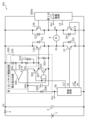
- FIG. 1 is a circuit block diagram showing a motor drive device of a first embodiment;
- FIG. It is a figure which shows the on-off operation
- It is a circuit block diagram which shows the motor drive device of a 2nd Example.
- It is a circuit block diagram which shows the motor drive device of 3rd Example.
- It is a circuit block diagram which shows the motor drive device of a 4th Example.
- the motor drive device when the voltage of the power supply line rises by a first threshold value or more, the high-side or low-side switching element in the off state is easily turned on. It is characterized by comprising a voltage detection circuit, a logic circuit, and a drive switch for turning on the switching element when the voltage rises above the second threshold.
- FIG. 1 is a circuit block diagram of a motor drive device 10 of a first embodiment according to the present disclosure.
- a motor driving device 10 is a device for driving a motor 4.
- the motor driving device 10 is connected to an input power supply 1 such as a battery, and includes a diode 2 and a capacitor 3 for preventing reverse battery connection. Let the voltage of the capacitor 3 be Vc.
- the input power source 1 may be an AC power source and the diode 2 may be a bridge diode.
- the motor driving device 10 also includes a control circuit 5 and receives power supply from a control circuit power source 6 .
- the voltage of the control circuit power supply 6 is assumed to be Vcc.
- the motor driving device 10 also receives power supply from the high-side driving power supply 7 .
- the high-side driving power supply 7 is a negative power supply with the positive electrode of the capacitor 3 as a reference potential.
- the voltage of the high-side drive power supply 7 is assumed to be Vcc'.
- the motor drive device 10 has a plurality of sets of series circuits of high-side switching elements and low-side switching elements connected between the power supply line and the ground, and an inductive load (motor 4) is connected to an intermediate connection point of each series circuit.
- the bridge circuit includes a first high-side transistor 11 made of a P-channel MOSFET, a first low-side transistor 12 made of an N-channel MOSFET, a second high-side transistor 13 made of a P-channel MOSFET, and an N-channel MOSFET. It is composed of a second low-side transistor 14 made of.
- the first high-side transistor 11, the first low-side transistor 12, the second high-side transistor 13, and the second low-side transistor 14 are hereinafter simply referred to as "transistors.”
- Transistors 11-14 have body diodes D1-D4, respectively, and constitute an H-bridge drive circuit for driving motor 4 using voltage Vc of capacitor 3 as a power supply voltage.
- the positive electrode of the capacitor 3 of the power supply voltage Vc is referred to as a power supply line
- the negative electrode of the capacitor 3 serving as the reference potential of the H-bridge drive circuit is referred to as a ground.
- a connection point between the first high-side transistor 11 and the first low-side transistor 12 is P1
- a connection point between the second high-side transistor 13 and the second low-side transistor 14 is P2.
- the control circuit 5 operates with the control circuit power supply voltage Vcc, and outputs drive signals t1', t2, t3' and t4 to the respective transistors 11-14.
- the drive signal t1' is a pre-drive signal to the first high-side transistor 11 (hereinafter also referred to as "pre-drive signal t1'")
- the drive signal t2 is a drive signal to the first low-side transistor 12
- the drive signal t3' is a pre-driving signal to the second high-side transistor 13 (hereinafter also referred to as "pre-driving signal t3'")
- the driving signal t4 is a driving signal to the second low-side transistor .
- the pre-drive signal t1' and the pre-drive signal t3' are signals having the high-side drive power supply voltage Vcc' as a reference potential, and are level-shifted in the control circuit 5 and output.
- the motor drive device 10 includes a first high side drive circuit 100 and a second high side drive circuit 100a.
- the first high-side driving circuit 100 receives the pre-driving signal t1' and turns the first high-side transistor 11 on and off.
- the second high-side drive circuit 100a receives the pre-drive signal t3' and turns the second high-side transistor 13 on and off.
- the first high-side drive circuit 100 is composed of a resistor 101 connected between the gate and source of the first high-side transistor 11, and a P-channel MOSFET, which short-circuits between the source and gate terminals of the first high-side transistor 11.
- a first drive transistor 102 connected to connect the gate terminal of the first high-side transistor 11 made of an N-channel MOSFET and a second drive transistor 102 connected to short-circuit between the high-side drive power supply 7 and the high-side drive power supply 7;
- a drive transistor 103 is included.
- the first drive transistor 102 is an example of a drive switch that is connected between the first terminal and the control terminal of the high-side switching element and opens and closes according to a drive signal.
- the first high-side drive circuit 100 includes a series circuit of a Zener diode 104 with a Zener voltage Vz1 and a detection resistor 105, which are connected between the gate terminal of the first high-side transistor 11 and the ground, and A comparator 106 is included. A connection point between Zener diode 104 and detection resistor 105 is connected to a positive input terminal of comparator 106 .
- voltage Vr is a reference voltage generated from control circuit power supply 6 and applied to the negative input terminal of comparator 106 .
- Zener diode 104, detection resistor 105, and comparator 106 become conductive when the voltage between the control terminal of the high-side switching element and the ground reaches or exceeds a first predetermined value, and the voltage between the control terminal of the high-side switching element and ground becomes conductive. It constitutes a voltage detection circuit 120 that outputs a detection signal indicating a first state when the voltage between the two becomes equal to or higher than a second predetermined value.
- the first high-side drive circuit 100 includes a level shift circuit 107 .
- the output of the comparator 106 that operates with the control circuit power supply voltage Vcc is converted via the level shift circuit 107 to the high side drive power supply voltage Vcc' reference.
- the pre-drive signal t1' is connected to the gate terminal of the second drive transistor 103.
- the first high-side drive circuit 100 also includes an OR circuit 108 to which the pre-drive signal t1' and the output signal of the level shift circuit 107 are input.
- the output of OR circuit 108 is connected to the gate terminal of first drive transistor 102 .
- the OR circuit 108 is an example of a logic circuit that opens the drive switch regardless of the drive signal when the detection signal from the voltage detection circuit 120 is in the first state.
- the configuration of the second high-side drive circuit 100a is the same as that of the first high-side drive circuit 100, so detailed illustration and description will be omitted.
- FIG. 2(a) shows that the first high-side transistor 11 and the second low-side transistor 14 are in an ON state, and the first high-side transistor 11, the motor 4, the second In this state, a current flows through the path to the ground (negative electrode of the capacitor 3) via the low-side transistor 14 of .
- a motor 4 which is an inductive load with coils, is energized and energy is stored.
- Capacitor 3 is discharged but is powered by input source 1 through diode 2 .
- FIG. 2(c) when the power supply voltage Vc exceeds a predetermined value, the first high-side transistor 11 is forcibly turned on and a loop is formed to discharge the capacitor 3. Suppress the rise of the voltage Vc.
- FIG. 2D shows that the first low-side transistor 12 and the second high-side transistor 13 are in the ON state, the discharge current flowing through the first high-side transistor 11 exceeds the regenerative current, and the capacitor 3 is discharged and the power supply voltage Vc turns to drop.
- the pre-drive signal t1' is at L level, the first drive transistor 102 is on, and the second drive transistor 103 is off. Therefore, the first high-side transistor 11 is in an off state, and the power supply voltage Vc is applied to the first high-side transistor 11 .
- the power supply voltage Vc rises and exceeds the Zener voltage Vz1 of the Zener diode 104 (that is, when the voltage between the control terminal of the high-side switching element and the ground reaches or exceeds a first predetermined value)
- the power supply line , first drive transistor 102 , Zener diode 104 and sense resistor 105 current flows to ground and a voltage is generated across sense resistor 105 .
- the comparator 106 Inverts the output from L level to H level (first state).
- the H level output of the comparator 106 is input to the OR circuit 108 via the level shift circuit 107, the output of the OR circuit 108 is inverted from the L level to the H level, and the first driving transistor 102 is turned off. .
- the current flowing through the first drive transistor 102 flows from the power supply line through the resistor 101, the Zener diode 104, and the detection resistor 105 to the ground.
- the discharge of the capacitor 3 causes the power supply voltage Vc to change from an increase to a decrease. Then, the source-gate voltage of the first high-side transistor 11 also drops, and when it falls below the gate threshold voltage, the first high-side transistor 11 is turned off. This prevents the discharge current of the capacitor 3 flowing through the first high-side transistor 11 from becoming excessive.
- the comparator 106 When the first drive transistor 102 turns off, the voltage difference between the power supply voltage Vc and the Zener voltage Vz1 is divided by the resistor 101 and the detection resistor 105, so the voltage of the detection resistor 105 drops. It is desirable that the comparator 106 have a hysteresis characteristic so that the output of the comparator 106 does not return to L level due to this drop.
- the operating current shown in FIG. 2 is also reversed. and the first low-side transistor 12 .
- the second high-side drive circuit 100a operates to turn on the second high-side transistor 13, thereby suppressing an increase in the power supply voltage Vc.
- an increase in the voltage applied to the switching elements forming the bridge circuit due to the regenerated power is suppressed.
- the motor drive device 10 includes a high-side switching element (first high-side transistor 11, etc.) and a low-side switching element (second 1 low-side transistor 12, etc.), and a bridge circuit in which the motor 4 is connected to the intermediate connection point of each series circuit. It has two terminals (drain terminal) and a control terminal (gate terminal), the first terminal is connected to the power supply line, the second terminal is connected to the low side switching element, and the high side switching element is connected to the first terminal and the control terminal. When a voltage equal to or higher than a predetermined threshold is applied between the first terminal and the second terminal, the motor driving device 10 further drives at least the high-side switching element.
- a control circuit 5 for outputting a drive signal for switching is connected between the control terminal of the high-side switching element and the ground, and the voltage between the control terminal of the high-side switching element and the ground is equal to or greater than a first predetermined value.
- a drive switch (first drive transistor 102) which is connected between the 1 terminal and the control terminal and which opens and closes according to the drive signal, and the detection signal from the voltage detection circuit 120 becomes the first state regardless of the drive signal.
- a logic circuit OR circuit 108) that opens the drive switch.
- the high-side switching element is forcibly turned on, suppressing the voltage rise of the power supply line and suppressing the rise of the voltage applied to the switching elements that make up the bridge circuit. be done.
- the voltage detection circuit 120 includes a series circuit of a first constant voltage device (Zener diode 104) having a first predetermined value and the detection resistor 105, and a connection point between the first constant voltage device and the detection resistor 105. and a comparator 106 that compares the potential of V with a predetermined reference voltage Vr and outputs a detection signal.
- a simple circuit suppresses an increase in the voltage applied to the switching element due to the regenerated power.
- FIG. 3 is a circuit block diagram showing the motor driving device 10a of the second embodiment.
- the same reference numerals are assigned to the same constituent elements as in FIG. 1, and the description thereof will be omitted.
- the difference is that the Zener diode 110 constituting the voltage detection circuit 121 is connected in parallel with the detection resistor 105, and the Zener voltage Vz0 of the Zener diode 110 is set higher than the reference voltage Vr.
- the first high-side drive circuit 130 of this embodiment includes the voltage detection circuit 121 to which the Zener diode 110 connected in parallel with the detection resistor 105 is added.
- the second high-side drive circuit 130a also includes a voltage detection circuit to which a Zener diode connected in parallel with the detection resistor is added. The operation of the motor driving device 10a of this embodiment to turn on the first high-side transistor 11 when the power supply voltage Vc exceeds a predetermined value will be described below.
- comparator 106 If this voltage is lower than reference voltage Vr, comparator 106 The output is at L level, and the output of level shift circuit 107 input to OR circuit 108 is also at L level. Accordingly, a signal voltage according to the pre-driving signal t1' is applied to the gate terminal of the first driving transistor 102, similarly to the second driving transistor 103.
- FIG. 1 A signal voltage according to the pre-driving signal t1' is applied to the gate terminal of the first driving transistor 102, similarly to the second driving transistor 103.
- the comparator 106 Inverts the output from L level to H level (first state).
- the H level output of the comparator 106 is input to the OR circuit 108 via the level shift circuit 107, the output of the OR circuit 108 is inverted from the L level to the H level, and the first driving transistor 102 is turned off. .
- the current flowing through the first drive transistor 102 flows from the power supply line through the resistor 101, the Zener diode 104, and the detection resistor 105 to the ground. - A voltage is generated across the gate. Eventually, the Zener diode 110 also becomes conductive, and when the source-gate voltage of the first high-side transistor 11 reaches the gate threshold value of the first high-side transistor 11, the first high-side transistor 11 becomes conductive.
- the voltage detection circuit 121 is connected in parallel with the detection resistor 105 in addition to the voltage detection circuit 120 of the first embodiment. It has a second constant voltage device (Zener diode 110) with a voltage higher than Vr.
- the first high-side transistor or the second high-side transistor is turned on to discharge the power supply voltage Vc, but the rise of the power supply voltage Vc can also be suppressed by turning on the low-side transistor. .
- FIG. 4 is a circuit block diagram showing the motor driving device 10b of the third embodiment.
- the same components as in FIG. 1 are denoted by the same reference numerals, and descriptions thereof are omitted.
- the difference is that the control circuit 5 of FIG.
- the point is that the drive circuit 200a is provided.
- control circuit 5a operates with the control circuit power supply voltage Vcc and outputs drive signals t1, t2', t3 and t4' to the respective transistors 11-14.
- the drive signal t1 is a drive signal for the first high-side transistor 11
- the drive signal t2' is a pre-drive signal for the first low-side transistor 12 (hereinafter also referred to as "pre-drive signal t2'")
- the drive signal t3 is
- the drive signal to the second high-side transistor 13, drive signal t4' is a pre-drive signal to the second low-side transistor 14 (hereinafter also referred to as "pre-drive signal t4'").
- the control circuit 5a includes a high-side drive power supply and a level shift circuit, and the drive signals t1 and t3 are directly transmitted to the gate terminals of the first high-side transistor 11 and the second high-side transistor 13. be done.
- the first low-side drive circuit 200 receives a pre-drive signal t2' to turn on and off the first low-side transistor 12, and the second low-side drive circuit 200a receives a pre-drive signal t4' to turn on and off the second low-side transistor 12. Turn transistor 14 on and off.
- the first low-side drive circuit 200 includes a resistor 201 connected between the gate and source of the first low-side transistor 12 and a P-channel MOSFET.
- a first drive transistor 202 connected to short-circuit between the gate and the source terminal of the first low-side transistor 12 consisting of an N-channel MOSFET, a second drive transistor 203 connected to short-circuit between the gate and source terminals of include.
- the second drive transistor 203 is an example of a drive switch that is connected between the control terminal and the second terminal of the low-side switching element and opens and closes according to the drive signal.
- the first low-side drive circuit 200 includes a series circuit of a Zener diode 204 with a Zener voltage Vz2 and a detection resistor 205, which are connected between the power supply line and the gate terminal of the first low-side transistor 12, and a comparison circuit. 206.
- a connection point between Zener diode 204 and detection resistor 205 is connected to a negative input terminal of comparator 206 .
- the voltage Vra is a reference voltage created from the control circuit power supply voltage Vcc and applied to the positive input terminal of the comparator 206 .
- Zener diode 204, detection resistor 205, and comparator 206 are connected between the power supply line and the control terminal of the low-side switching element, and the voltage between the power supply line and the control terminal of the low-side switching element is equal to or greater than a first predetermined value.
- the voltage detection circuit 220 forms a voltage detection circuit 220 which is turned on when the voltage rises, and which outputs a detection signal indicating the first state when the voltage between the power supply line and the control terminal of the low-side switching element becomes equal to or higher than the second predetermined value.
- the first low-side drive circuit 200 also includes an AND circuit 207 to which the pre-drive signal t2' and the output signal of the comparator 206 are input.
- the output of AND circuit 207 is connected to the gate terminal of second drive transistor 203 .
- the AND circuit 207 is an example of a logic circuit that opens the drive switch regardless of the drive signal when the detection signal from the voltage detection circuit 220 is in the first state.
- the configuration of the second low-side driving circuit 200a is the same as that of the first low-side driving circuit 200, so detailed illustration and description will be omitted.
- the second high-side transistor 13 and the first low-side transistor 12 are applied with the power supply voltage Vc that is charged during the energized phase switching operation, which is opposite in phase to that in FIG.
- the operation of the motor driving device 10b of this embodiment shown in FIG. 4 in which the first low-side driving circuit 200 turns on the first low-side transistor 12 when the power supply voltage Vc exceeds a predetermined value will be described below.
- the first drive transistor 202 is in the ON state, and the output of the AND circuit 207 is also at L level regardless of the output state of the comparator 206.
- the transistor 203 is turned off.
- a gate voltage at the control circuit power supply voltage Vcc level is applied to the first low-side transistor 12, and the first low-side transistor 12 is turned on.
- the gate voltage is also applied to the negative input terminal of the comparator 206 via the detection resistor 205, and the output of the comparator 206 is at L level.
- the first drive transistor 202 is in the off state. Further, in the normal state where the power supply voltage Vc is equal to or lower than the Zener voltage Vz2 of the Zener diode 204, the first low-side transistor 12 with no voltage supplied to the gate terminal is in the off state. A voltage equal to or higher than the voltage Vra does not occur at the negative input terminal of the comparator 206, the output of the comparator 206 becomes H level, the output of the AND circuit 207 becomes H level, and the second drive transistor 203 is turned on. As a result, the first low-side transistor 12 whose gate terminal is grounded maintains the off state.
- the Zener diode Current flows through 204 , sense resistor 205 and second drive transistor 203 to ground, generating a voltage across sense resistor 205 .
- the voltage of the detection resistor 205 that is, the negative input terminal of the comparator 206 generates a voltage equal to or higher than the voltage Vra as the power supply voltage Vc rises (that is, the voltage between the power supply line and the control terminal of the low-side switching element increases to the second exceeds a predetermined value)
- the output of the comparator 206 becomes L level (first state)
- the output of the AND circuit 207 also becomes L level
- the second driving transistor 203 is turned off. Then, the current flowing through the second drive transistor 203 starts to flow from the power supply line to the ground via the Zener diode 204, the detection resistor 205, and the resistor 201, and the gate terminal of the first low-side transistor 12. voltage is generated.
- the first low-side transistor 12 When this voltage reaches the gate threshold of the first low-side transistor 12, the first low-side transistor 12 becomes conductive, creating a loop that discharges the capacitor 3 via the first high-side transistor 11, thereby increasing the supply voltage Vc. suppress the increase in As a result, an increase in the voltage applied to the switching elements forming the bridge circuit due to the regenerated power is suppressed.
- the discharge current flowing through the first low-side transistor 12 exceeds the regenerative current of the motor, and the discharge of the capacitor 3 reduces the power supply voltage Vc. It turns from an increase to a decrease. Then, the gate-source voltage of the first low-side transistor 12 also drops, and when it falls below the gate threshold voltage, the first low-side transistor 12 is turned off. This prevents the discharge current of the capacitor 3 flowing through the first low-side transistor 12 from becoming excessive.
- the first high-side transistor 11 and the second low-side transistor 11 are applied with the power supply voltage Vc charged during the energized phase switching operation. It is the transistor 14 .
- the second low-side drive circuit 200a operates to turn on the second low-side transistor 14, thereby suppressing an increase in the power supply voltage Vc. As a result, an increase in the voltage applied to the switching elements forming the bridge circuit due to the regenerated power is suppressed.
- the Zener diode 210 forming the voltage detection circuit 220 may be connected in parallel with the detection resistor 205 in this embodiment as well.
- the motor drive device 10b includes a high-side switching element (first high-side transistor 11, etc.) and a low-side switching element (second 1 low side transistor 12, etc.), a bridge circuit is provided in which the motor 4 is connected to the intermediate connection point of each series circuit, and the low side switching element has a first terminal (drain terminal) and a second terminal (source terminal) and a control terminal (gate terminal), the first terminal being connected to the high side switching element, the second terminal being connected to ground, and the low side switching element being between the control terminal and the second terminal.
- the motor driving device 10b has a function of establishing conduction between the first terminal and the second terminal when a voltage equal to or higher than a predetermined threshold is applied, and the motor driving device 10b further outputs a driving signal for driving at least the low-side switching element. and a control circuit 5a connected between the power supply line and the control terminal of the low-side switching element.
- a voltage detection circuit 220 that outputs a detection signal to be in the first state when the voltage between the control terminal of the low-side switching element and the control terminal of the low-side switching element reaches or exceeds a second predetermined value; and a drive switch (second drive transistor 203) that opens and closes according to the drive signal, and logic that opens the drive switch regardless of the drive signal when the detection signal from the voltage detection circuit 220 is in the first state.
- circuit (AND circuit 207)
- the low-side switching element is forcibly turned on, suppressing the voltage rise of the power supply line and suppressing the rise of the voltage applied to the switching elements constituting the bridge circuit.
- the voltage detection circuit 220 includes a series circuit of a first constant voltage device (Zener diode 204) having a first predetermined value and the detection resistor 205, and a connection point between the first constant voltage device and the detection resistor 205. and a comparator 206 that compares the potential with a predetermined reference voltage Vr and outputs a detection signal.
- a simple circuit suppresses an increase in the voltage applied to the switching element due to the regenerated power.
- the voltage detection circuit 220 further has a second constant voltage device (Zener diode 210) connected in parallel with the detection resistor 205 and having a voltage higher than the predetermined reference voltage Vr.
- a second constant voltage device Zener diode 210 connected in parallel with the detection resistor 205 and having a voltage higher than the predetermined reference voltage Vr.
- the first or second high-side transistor is a P-channel MOSFET, but even if it is an N-channel MOSFET, it is possible to suppress the rise of the power supply voltage Vc.
- FIG. 5 is a circuit block diagram showing the motor driving device 10c of the fourth embodiment.
- the same components as in FIG. 1 are denoted by the same reference numerals, and descriptions thereof are omitted.
- the first or second high-side transistors are N-channel MOSFETs, which are referred to as a first high-side transistor 11b and a second high-side transistor 13b for distinction from FIG.
- the control circuit 5 of FIG. 1 is replaced with the control circuit 5b, and the configurations of the first high side driving circuit 100 and the second high side driving circuit 100a of FIG. 1 is provided with a high side drive circuit 300a.
- the control circuit 5b operates with the control circuit power supply voltage Vcc, and outputs drive signals t1'', t2, t3'' and t4 for the respective transistors 11b, 12, 13b and 14.
- the drive signal t1'' is a pre-drive signal (hereinafter also referred to as "pre-drive signal t1''") to the first high-side transistor 11b
- the drive signal t2 is a drive signal to the first low-side transistor 12
- the drive signal t3'' is a pre-driving signal to the second high-side transistor 13b (hereinafter also referred to as "pre-driving signal t3''")
- the driving signal t4 is a driving signal to the second low-side transistor .
- the first high-side drive circuit 300 receives the pre-drive signal t1'' to turn on/off the first high-side transistor 11b
- the second high-side drive circuit 300a receives the pre-drive signal t3'' to turn on and off the first high-side transistor 11b.
- 2 high-side transistor 13b is turned on and off.
- the control circuit 5b includes a level shift circuit, and the drive signals t1'' and t3'' are signals whose reference potential is the source terminal potential of the first high-side transistor 11b and the second high-side transistor 13b. is converted to
- the high-side drive power supply voltage Vbc is created by a bootstrap circuit, which will be described later.
- the first high-side drive circuit 300 includes a resistor 301 connected between the gate and source of the first high-side transistor 11b and a P-channel MOSFET.
- a first drive transistor 302 connected to short-circuit between the power supply voltage Vbc and a second drive transistor 302 made of an N-channel MOSFET and connected to short-circuit between the gate and source terminals of the first high-side transistor 11b.
- drive transistor 303 is an example of a drive switch that is connected between the control terminal and the second terminal of the high-side switching element and opens and closes according to the drive signal.
- the first high-side drive circuit 300 includes a series circuit of a Zener diode 304 with a Zener voltage Vz3 and a detection resistor 305, which are connected between the power supply line and the gate terminal of the first high-side transistor 11b, and , including a comparator 306 .
- a connection point between Zener diode 304 and detection resistor 305 is connected to a negative input terminal of comparator 306 .
- the voltage Vrb is a reference voltage created from the high-side driving power supply voltage Vbc and applied to the positive input terminal of the comparator 306 .
- the Zener diode 304, the detection resistor 305 and the comparator 306 are connected between the power supply line and the control terminal of the high side switching element so that the voltage between the power supply line and the control terminal of the high side switching element is a first predetermined value.
- the voltage detection circuit 320 outputs a detection signal that is in the first state. .
- the first high-side drive circuit 300 also includes an AND circuit 307 to which the pre-drive signal t1′′ and the output signal of the comparator 306 are input. applied.
- the output of AND circuit 307 is connected to the gate terminal of second drive transistor 303 .
- the AND circuit 307 is an example of a logic circuit that opens the drive switch regardless of the drive signal when the detection signal from the voltage detection circuit 320 is in the first state.
- the first high-side drive circuit 300 includes a diode 308 and a capacitor 309 .
- the diode 308 and the capacitor 309 charge the capacitor 309 from the control circuit power supply voltage Vcc through the diode 308 when the first low-side transistor 12 is turned on, thereby causing the capacitor 309 to generate the high-side drive power supply voltage Vbc.
- It is a strap circuit.
- the configuration of the second high-side drive circuit 300a is the same as that of the first high-side drive circuit 300, so illustration and description thereof are omitted.
- the first drive transistor 302 is in the ON state, and the high-side drive power supply voltage Vbc is applied to the gate terminal of the first high-side transistor 11b.
- the negative input terminal of the comparator 306 is dropped to the source terminal of the first high-side transistor 11b via the Zener diode 304, and no voltage is generated.
- the comparator 306 outputs an H level.
- the AND circuit 307 receiving the L level pre-drive signal t1'' outputs an L level
- the second driving transistor 303 is in an off state, and the first maintains the ON state.
- the first drive transistor 302 is in the OFF state. Further, in the normal state where the power supply voltage Vc is equal to or lower than the Zener voltage Vz3 of the Zener diode 304, the voltage to the gate terminal is The first high-side transistor 11b to which no voltage is supplied is in an off state, and a voltage equal to or higher than the voltage Vrb does not occur at the negative input terminal of the comparator 306, and the output of the comparator 306 becomes H level. The output becomes H level, the second drive transistor 303 is turned on, and the first high-side transistor 11b whose gate terminal is grounded maintains the off state.
- the Zener A current flows to ground through the diode 304 , the sensing resistor 305 , the second driving transistor 303 and the first low-side transistor 12 , and a voltage is generated across the sensing resistor 305 .
- the voltage of the detection resistor 305 that is, the negative input terminal of the comparator 306 generates a voltage equal to or higher than the voltage Vrb as the power supply voltage Vc rises (that is, the voltage between the power supply line and the control terminal of the high-side switching element rises to the first 2)
- the output of the comparator 306 becomes L level (first state)
- the output of the AND circuit 307 also becomes L level
- the second drive transistor 303 is turned off.
- the current flowing through the second drive transistor 303 flows from the power supply line through the Zener diode 304, the detection resistor 305, the resistor 301, and the first low-side transistor 12 to the ground.
- a voltage is generated at the gate terminal of the high-side transistor 11b.
- the first high-side transistor 11b When this voltage reaches the gate threshold value of the first high-side transistor 11b, the first high-side transistor 11b becomes conductive, creating a loop that discharges the capacitor 3, thereby suppressing the rise of the power supply voltage Vc. As a result, an increase in the voltage applied to the switching elements forming the bridge circuit due to the regenerated power is suppressed.
- the discharge current flowing through the first high-side transistor 11b exceeds the regenerative current of the motor, and the discharge of the capacitor 3 reduces the power supply voltage Vc. It turns from an increase to a decrease. Then, the gate-source voltage of the first high-side transistor 11b also drops, and when it falls below the gate threshold voltage, the first high-side transistor 11b is turned off. This prevents the discharge current of the capacitor 3 flowing through the first high-side transistor 11b from becoming excessive.
- the operating current is also reversed, and the power supply voltage Vc charged during the energized phase switching operation is applied to the second high-side transistor 13b and the first low-side transistor 12. is.
- the second high-side drive circuit 300a operates to turn on the second high-side transistor 13b, thereby suppressing an increase in the power supply voltage Vc.
- an increase in the voltage applied to the switching elements forming the bridge circuit due to the regenerated power is suppressed.
- the Zener diode 310 forming the voltage detection circuit 320 may be connected in parallel with the detection resistor 305 in this embodiment as well.
- the subsequent increase in the power supply voltage Vc is added to the gate voltage of the first high-side transistor 11b, the on-resistance between the drain and source of the first high-side transistor 11b rapidly decreases, increasing the discharge current. . Therefore, the effect of suppressing the rise of the power supply voltage Vc is improved. As a result, an increase in the voltage applied to the switching elements forming the bridge circuit due to the regenerated power is more reliably suppressed.
- the motor drive device 10c includes a high-side switching element (first high-side transistor 11b, etc.) and a low-side switching element (second 1 low-side transistor 12, etc.), and a bridge circuit in which the motor 4 is connected to the intermediate connection point of each series circuit. It has a terminal (source terminal) and a control terminal (gate terminal), the first terminal is connected to the power supply line, the second terminal is connected to the low side switching element, and the high side switching element is connected between the control terminal and the second terminal.
- the motor driving device 10c has a function of establishing conduction between the first terminal and the second terminal when a voltage equal to or higher than a predetermined threshold is applied between the first terminal and the second terminal.
- a control circuit 5b for outputting a signal is connected between the power supply line and the control terminal of the high-side switching element, and when the voltage between the power supply line and the control terminal of the high-side switching element reaches or exceeds a first predetermined value.
- a voltage detection circuit 320 which is turned on and outputs a detection signal to enter the first state when the voltage between the power supply line and the control terminal of the high side switching element reaches a second predetermined value or more, and the control terminal of the high side switching element. and a second terminal and is opened and closed according to a drive signal, and a drive switch (second drive transistor 303) that opens and closes according to a drive signal, and when the detection signal from the voltage detection circuit 320 becomes the first state, the drive is driven regardless of the drive signal. and a logic circuit (AND circuit 307) that opens the switch.
- the high-side switching element is forcibly turned on, suppressing the voltage rise of the power supply line and suppressing the rise of the voltage applied to the switching elements that make up the bridge circuit. be done.
- the voltage detection circuit 320 includes a series circuit of a first constant voltage device (Zener diode 304) having a first predetermined value and the detection resistor 305, and a connection point between the first constant voltage device and the detection resistor 305. and a comparator 306 that compares the potential with a predetermined reference voltage Vr and outputs a detection signal.
- a simple circuit suppresses an increase in the voltage applied to the switching element due to the regenerated power.
- the voltage detection circuit 320 also has a second constant voltage device (Zener diode 310) connected in parallel with the detection resistor 305 and having a voltage higher than the predetermined reference voltage Vr.
- the voltage detection circuit is not limited to the circuit shown in each embodiment, and may be a first comparator having a first predetermined value as a threshold and a second comparator having a second predetermined value as a threshold. may be configured.
- the comparator that constitutes the voltage detection circuit does not necessarily need to be configured with an operational amplifier (IC), and may be a discrete circuit configured with transistors.
- IC operational amplifier
- control circuits 5, 5a, and 5b do not necessarily have to be provided in the motor driving device, and may be external devices that provide drive signals to the motor driving device. Also, the control circuits 5, 5a and 5b may be composed of an IC, a discrete circuit, or a combination thereof.
- the motor drive device can be used as a motor drive device having an overvoltage protection function, particularly as a motor drive device capable of suppressing an increase in voltage applied to switching elements due to regenerated power.
Landscapes
- Engineering & Computer Science (AREA)
- Power Engineering (AREA)
- Control Of Direct Current Motors (AREA)
- Inverter Devices (AREA)
- Electronic Switches (AREA)
Priority Applications (5)
| Application Number | Priority Date | Filing Date | Title |
|---|---|---|---|
| CN202280076020.XA CN118266172A (zh) | 2021-11-19 | 2022-11-07 | 马达驱动装置 |
| JP2023561535A JPWO2023090187A1 (https=) | 2021-11-19 | 2022-11-07 | |
| JP2024063283A JP2024104752A (ja) | 2021-11-19 | 2024-04-10 | モータ駆動装置 |
| JP2024063282A JP2024105260A (ja) | 2021-11-19 | 2024-04-10 | モータ駆動装置 |
| US18/656,083 US12592691B2 (en) | 2021-11-19 | 2024-05-06 | Motor driving device |
Applications Claiming Priority (2)
| Application Number | Priority Date | Filing Date | Title |
|---|---|---|---|
| JP2021189003 | 2021-11-19 | ||
| JP2021-189003 | 2021-11-19 |
Related Child Applications (1)
| Application Number | Title | Priority Date | Filing Date |
|---|---|---|---|
| US18/656,083 Continuation US12592691B2 (en) | 2021-11-19 | 2024-05-06 | Motor driving device |
Publications (1)
| Publication Number | Publication Date |
|---|---|
| WO2023090187A1 true WO2023090187A1 (ja) | 2023-05-25 |
Family
ID=86396932
Family Applications (1)
| Application Number | Title | Priority Date | Filing Date |
|---|---|---|---|
| PCT/JP2022/041378 Ceased WO2023090187A1 (ja) | 2021-11-19 | 2022-11-07 | モータ駆動装置 |
Country Status (4)
| Country | Link |
|---|---|
| US (1) | US12592691B2 (https=) |
| JP (3) | JPWO2023090187A1 (https=) |
| CN (1) | CN118266172A (https=) |
| WO (1) | WO2023090187A1 (https=) |
Families Citing this family (1)
| Publication number | Priority date | Publication date | Assignee | Title |
|---|---|---|---|---|
| JP2024107888A (ja) * | 2023-01-30 | 2024-08-09 | ローム株式会社 | ブリッジ回路の駆動回路、それを用いたモータ駆動装置、電子機器 |
Citations (4)
| Publication number | Priority date | Publication date | Assignee | Title |
|---|---|---|---|---|
| JPH0191620A (ja) * | 1987-10-02 | 1989-04-11 | Hitachi Ltd | Hブリツジ保護回路 |
| JPH06245585A (ja) * | 1993-02-21 | 1994-09-02 | Nissan Motor Co Ltd | 半導体装置 |
| JPH0884055A (ja) * | 1994-09-14 | 1996-03-26 | Nissan Motor Co Ltd | ハイサイドスイッチ回路 |
| JP2005269885A (ja) * | 2004-02-16 | 2005-09-29 | Denso Corp | Hブリッジ回路の駆動装置及びhブリッジ回路の保護方法 |
Family Cites Families (6)
| Publication number | Priority date | Publication date | Assignee | Title |
|---|---|---|---|---|
| JPH1070897A (ja) | 1996-08-27 | 1998-03-10 | Meidensha Corp | 直流電動機の制御回路 |
| JP5803950B2 (ja) * | 2013-02-05 | 2015-11-04 | 株式会社デンソー | スイッチング素子の駆動装置 |
| WO2017037916A1 (ja) * | 2015-09-03 | 2017-03-09 | 三菱電機株式会社 | 電力変換装置 |
| JP6665573B2 (ja) * | 2016-02-17 | 2020-03-13 | 富士電機株式会社 | スイッチング電源装置 |
| JP7184038B2 (ja) * | 2017-07-31 | 2022-12-06 | 日本電産株式会社 | 電力変換装置、モータモジュールおよび電動パワーステアリング装置 |
| JP6988670B2 (ja) * | 2018-04-24 | 2022-01-05 | 三菱電機株式会社 | 駆動回路、パワーモジュール及び電力変換システム |
-
2022
- 2022-11-07 WO PCT/JP2022/041378 patent/WO2023090187A1/ja not_active Ceased
- 2022-11-07 CN CN202280076020.XA patent/CN118266172A/zh active Pending
- 2022-11-07 JP JP2023561535A patent/JPWO2023090187A1/ja active Pending
-
2024
- 2024-04-10 JP JP2024063282A patent/JP2024105260A/ja active Pending
- 2024-04-10 JP JP2024063283A patent/JP2024104752A/ja active Pending
- 2024-05-06 US US18/656,083 patent/US12592691B2/en active Active
Patent Citations (4)
| Publication number | Priority date | Publication date | Assignee | Title |
|---|---|---|---|---|
| JPH0191620A (ja) * | 1987-10-02 | 1989-04-11 | Hitachi Ltd | Hブリツジ保護回路 |
| JPH06245585A (ja) * | 1993-02-21 | 1994-09-02 | Nissan Motor Co Ltd | 半導体装置 |
| JPH0884055A (ja) * | 1994-09-14 | 1996-03-26 | Nissan Motor Co Ltd | ハイサイドスイッチ回路 |
| JP2005269885A (ja) * | 2004-02-16 | 2005-09-29 | Denso Corp | Hブリッジ回路の駆動装置及びhブリッジ回路の保護方法 |
Also Published As
| Publication number | Publication date |
|---|---|
| CN118266172A (zh) | 2024-06-28 |
| JP2024104752A (ja) | 2024-08-05 |
| US12592691B2 (en) | 2026-03-31 |
| US20240291477A1 (en) | 2024-08-29 |
| JPWO2023090187A1 (https=) | 2023-05-25 |
| JP2024105260A (ja) | 2024-08-06 |
Similar Documents
| Publication | Publication Date | Title |
|---|---|---|
| JP5590031B2 (ja) | 電源保護回路およびそれを備えたモータ駆動装置 | |
| US7592831B2 (en) | Circuit to optimize charging of bootstrap capacitor with bootstrap diode emulator | |
| US10355472B2 (en) | Over temperature protection circuit and semiconductor device | |
| US9871440B2 (en) | Internal power supply circuit and semiconductor device | |
| CN100449929C (zh) | 反相器电路 | |
| JP2007089393A (ja) | 弱め界磁で作動する永久磁石同期発電機の安全回路 | |
| WO2016204122A1 (ja) | 半導体装置 | |
| JP4018077B2 (ja) | 電力用スイッチのためのバッテリ逆接続の保護回路 | |
| JP2002290221A (ja) | 半導体出力回路の消費電力低減回路 | |
| CN114204926A (zh) | 半导体装置 | |
| JP7095388B2 (ja) | トーテムポール回路用駆動装置 | |
| JP4792636B2 (ja) | 誘導性負荷駆動回路 | |
| JP2017017688A (ja) | 電界効果トランジスタを備えたパワー半導体回路 | |
| US20080136466A1 (en) | Semiconductor Integrated Circuit Driving External FET and Power Supply Incorporating the Same | |
| WO2023090187A1 (ja) | モータ駆動装置 | |
| US6369533B1 (en) | Piloting circuit for an inductive load in particular for a DC electric motor | |
| WO2001059918A1 (fr) | Dispositif onduleur | |
| US8138705B2 (en) | Circuit arrangement and method for controlling an electric load | |
| JP7247903B2 (ja) | 電気回路及び電源装置 | |
| JP7225601B2 (ja) | トーテムポール回路用駆動装置 | |
| JP4479570B2 (ja) | 保護機能付きスイッチング回路および保護回路 | |
| JPH11215871A (ja) | モータ制御装置 | |
| US4977477A (en) | Short-circuit protected switched output circuit | |
| JP3191661B2 (ja) | 半導体素子の過負荷保護回路 | |
| JP5226474B2 (ja) | 半導体出力回路 |
Legal Events
| Date | Code | Title | Description |
|---|---|---|---|
| 121 | Ep: the epo has been informed by wipo that ep was designated in this application |
Ref document number: 22895469 Country of ref document: EP Kind code of ref document: A1 |
|
| ENP | Entry into the national phase |
Ref document number: 2023561535 Country of ref document: JP Kind code of ref document: A |
|
| WWE | Wipo information: entry into national phase |
Ref document number: 202280076020.X Country of ref document: CN |
|
| NENP | Non-entry into the national phase |
Ref country code: DE |
|
| 122 | Ep: pct application non-entry in european phase |
Ref document number: 22895469 Country of ref document: EP Kind code of ref document: A1 |