WO2023080081A1 - 半導体装置 - Google Patents
半導体装置 Download PDFInfo
- Publication number
- WO2023080081A1 WO2023080081A1 PCT/JP2022/040493 JP2022040493W WO2023080081A1 WO 2023080081 A1 WO2023080081 A1 WO 2023080081A1 JP 2022040493 W JP2022040493 W JP 2022040493W WO 2023080081 A1 WO2023080081 A1 WO 2023080081A1
- Authority
- WO
- WIPO (PCT)
- Prior art keywords
- electrode
- source
- gap
- gate
- semiconductor device
- Prior art date
- Legal status (The legal status is an assumption and is not a legal conclusion. Google has not performed a legal analysis and makes no representation as to the accuracy of the status listed.)
- Ceased
Links
Images


Classifications
-
- H—ELECTRICITY
- H10—SEMICONDUCTOR DEVICES; ELECTRIC SOLID-STATE DEVICES NOT OTHERWISE PROVIDED FOR
- H10D—INORGANIC ELECTRIC SEMICONDUCTOR DEVICES
- H10D64/00—Electrodes of devices having potential barriers
- H10D64/20—Electrodes characterised by their shapes, relative sizes or dispositions
- H10D64/23—Electrodes carrying the current to be rectified, amplified, oscillated or switched, e.g. sources, drains, anodes or cathodes
- H10D64/251—Source or drain electrodes for field-effect devices
- H10D64/252—Source or drain electrodes for field-effect devices for vertical or pseudo-vertical devices
-
- H—ELECTRICITY
- H10—SEMICONDUCTOR DEVICES; ELECTRIC SOLID-STATE DEVICES NOT OTHERWISE PROVIDED FOR
- H10D—INORGANIC ELECTRIC SEMICONDUCTOR DEVICES
- H10D12/00—Bipolar devices controlled by the field effect, e.g. insulated-gate bipolar transistors [IGBT]
- H10D12/411—Insulated-gate bipolar transistors [IGBT]
- H10D12/441—Vertical IGBTs
- H10D12/461—Vertical IGBTs having non-planar surfaces, e.g. having trenches, recesses or pillars in the surfaces of the emitter, base or collector regions
- H10D12/481—Vertical IGBTs having non-planar surfaces, e.g. having trenches, recesses or pillars in the surfaces of the emitter, base or collector regions having gate structures on slanted surfaces, on vertical surfaces, or in grooves, e.g. trench gate IGBTs
-
- H—ELECTRICITY
- H10—SEMICONDUCTOR DEVICES; ELECTRIC SOLID-STATE DEVICES NOT OTHERWISE PROVIDED FOR
- H10D—INORGANIC ELECTRIC SEMICONDUCTOR DEVICES
- H10D30/00—Field-effect transistors [FET]
- H10D30/60—Insulated-gate field-effect transistors [IGFET]
- H10D30/64—Double-diffused metal-oxide semiconductor [DMOS] FETs
- H10D30/66—Vertical DMOS [VDMOS] FETs
- H10D30/665—Vertical DMOS [VDMOS] FETs having edge termination structures
-
- H—ELECTRICITY
- H10—SEMICONDUCTOR DEVICES; ELECTRIC SOLID-STATE DEVICES NOT OTHERWISE PROVIDED FOR
- H10D—INORGANIC ELECTRIC SEMICONDUCTOR DEVICES
- H10D30/00—Field-effect transistors [FET]
- H10D30/60—Insulated-gate field-effect transistors [IGFET]
- H10D30/64—Double-diffused metal-oxide semiconductor [DMOS] FETs
- H10D30/66—Vertical DMOS [VDMOS] FETs
- H10D30/668—Vertical DMOS [VDMOS] FETs having trench gate electrodes, e.g. UMOS transistors
-
- H—ELECTRICITY
- H10—SEMICONDUCTOR DEVICES; ELECTRIC SOLID-STATE DEVICES NOT OTHERWISE PROVIDED FOR
- H10D—INORGANIC ELECTRIC SEMICONDUCTOR DEVICES
- H10D62/00—Semiconductor bodies, or regions thereof, of devices having potential barriers
- H10D62/10—Shapes, relative sizes or dispositions of the regions of the semiconductor bodies; Shapes of the semiconductor bodies
- H10D62/102—Constructional design considerations for preventing surface leakage or controlling electric field concentration
- H10D62/103—Constructional design considerations for preventing surface leakage or controlling electric field concentration for increasing or controlling the breakdown voltage of reverse-biased devices
- H10D62/105—Constructional design considerations for preventing surface leakage or controlling electric field concentration for increasing or controlling the breakdown voltage of reverse-biased devices by having particular doping profiles, shapes or arrangements of PN junctions; by having supplementary regions, e.g. junction termination extension [JTE]
- H10D62/106—Constructional design considerations for preventing surface leakage or controlling electric field concentration for increasing or controlling the breakdown voltage of reverse-biased devices by having particular doping profiles, shapes or arrangements of PN junctions; by having supplementary regions, e.g. junction termination extension [JTE] having supplementary regions doped oppositely to or in rectifying contact with regions of the semiconductor bodies, e.g. guard rings with PN or Schottky junctions
- H10D62/107—Buried supplementary regions, e.g. buried guard rings
-
- H—ELECTRICITY
- H10—SEMICONDUCTOR DEVICES; ELECTRIC SOLID-STATE DEVICES NOT OTHERWISE PROVIDED FOR
- H10D—INORGANIC ELECTRIC SEMICONDUCTOR DEVICES
- H10D62/00—Semiconductor bodies, or regions thereof, of devices having potential barriers
- H10D62/10—Shapes, relative sizes or dispositions of the regions of the semiconductor bodies; Shapes of the semiconductor bodies
- H10D62/124—Shapes, relative sizes or dispositions of the regions of semiconductor bodies or of junctions between the regions
- H10D62/126—Top-view geometrical layouts of the regions or the junctions
- H10D62/127—Top-view geometrical layouts of the regions or the junctions of cellular field-effect devices, e.g. multicellular DMOS transistors or IGBTs
-
- H—ELECTRICITY
- H10—SEMICONDUCTOR DEVICES; ELECTRIC SOLID-STATE DEVICES NOT OTHERWISE PROVIDED FOR
- H10D—INORGANIC ELECTRIC SEMICONDUCTOR DEVICES
- H10D62/00—Semiconductor bodies, or regions thereof, of devices having potential barriers
- H10D62/10—Shapes, relative sizes or dispositions of the regions of the semiconductor bodies; Shapes of the semiconductor bodies
- H10D62/17—Semiconductor regions connected to electrodes not carrying current to be rectified, amplified or switched, e.g. channel regions
- H10D62/393—Body regions of DMOS transistors or IGBTs
-
- H—ELECTRICITY
- H10—SEMICONDUCTOR DEVICES; ELECTRIC SOLID-STATE DEVICES NOT OTHERWISE PROVIDED FOR
- H10D—INORGANIC ELECTRIC SEMICONDUCTOR DEVICES
- H10D62/00—Semiconductor bodies, or regions thereof, of devices having potential barriers
- H10D62/80—Semiconductor bodies, or regions thereof, of devices having potential barriers characterised by the materials
- H10D62/83—Semiconductor bodies, or regions thereof, of devices having potential barriers characterised by the materials being Group IV materials, e.g. B-doped Si or undoped Ge
- H10D62/832—Semiconductor bodies, or regions thereof, of devices having potential barriers characterised by the materials being Group IV materials, e.g. B-doped Si or undoped Ge being Group IV materials comprising two or more elements, e.g. SiGe
- H10D62/8325—Silicon carbide
-
- H—ELECTRICITY
- H10—SEMICONDUCTOR DEVICES; ELECTRIC SOLID-STATE DEVICES NOT OTHERWISE PROVIDED FOR
- H10D—INORGANIC ELECTRIC SEMICONDUCTOR DEVICES
- H10D64/00—Electrodes of devices having potential barriers
- H10D64/111—Field plates
- H10D64/117—Recessed field plates, e.g. trench field plates or buried field plates
-
- H—ELECTRICITY
- H10—SEMICONDUCTOR DEVICES; ELECTRIC SOLID-STATE DEVICES NOT OTHERWISE PROVIDED FOR
- H10D—INORGANIC ELECTRIC SEMICONDUCTOR DEVICES
- H10D64/00—Electrodes of devices having potential barriers
- H10D64/20—Electrodes characterised by their shapes, relative sizes or dispositions
- H10D64/23—Electrodes carrying the current to be rectified, amplified, oscillated or switched, e.g. sources, drains, anodes or cathodes
- H10D64/251—Source or drain electrodes for field-effect devices
- H10D64/252—Source or drain electrodes for field-effect devices for vertical or pseudo-vertical devices
- H10D64/2527—Source or drain electrodes for field-effect devices for vertical or pseudo-vertical devices for vertical devices wherein the source or drain electrodes are recessed in semiconductor bodies
-
- H—ELECTRICITY
- H10—SEMICONDUCTOR DEVICES; ELECTRIC SOLID-STATE DEVICES NOT OTHERWISE PROVIDED FOR
- H10W—GENERIC PACKAGES, INTERCONNECTIONS, CONNECTORS OR OTHER CONSTRUCTIONAL DETAILS OF DEVICES COVERED BY CLASS H10
- H10W70/00—Package substrates; Interposers; Redistribution layers [RDL]
- H10W70/40—Leadframes
- H10W70/411—Chip-supporting parts, e.g. die pads
- H10W70/417—Bonding materials between chips and die pads
-
- H—ELECTRICITY
- H10—SEMICONDUCTOR DEVICES; ELECTRIC SOLID-STATE DEVICES NOT OTHERWISE PROVIDED FOR
- H10W—GENERIC PACKAGES, INTERCONNECTIONS, CONNECTORS OR OTHER CONSTRUCTIONAL DETAILS OF DEVICES COVERED BY CLASS H10
- H10W70/00—Package substrates; Interposers; Redistribution layers [RDL]
- H10W70/40—Leadframes
- H10W70/464—Additional interconnections in combination with leadframes
- H10W70/465—Bumps or wires
-
- H—ELECTRICITY
- H10—SEMICONDUCTOR DEVICES; ELECTRIC SOLID-STATE DEVICES NOT OTHERWISE PROVIDED FOR
- H10W—GENERIC PACKAGES, INTERCONNECTIONS, CONNECTORS OR OTHER CONSTRUCTIONAL DETAILS OF DEVICES COVERED BY CLASS H10
- H10W70/00—Package substrates; Interposers; Redistribution layers [RDL]
- H10W70/40—Leadframes
- H10W70/481—Leadframes for devices being provided for in groups H10D8/00 - H10D48/00
-
- H—ELECTRICITY
- H10—SEMICONDUCTOR DEVICES; ELECTRIC SOLID-STATE DEVICES NOT OTHERWISE PROVIDED FOR
- H10W—GENERIC PACKAGES, INTERCONNECTIONS, CONNECTORS OR OTHER CONSTRUCTIONAL DETAILS OF DEVICES COVERED BY CLASS H10
- H10W74/00—Encapsulations, e.g. protective coatings
- H10W74/10—Encapsulations, e.g. protective coatings characterised by their shape or disposition
- H10W74/111—Encapsulations, e.g. protective coatings characterised by their shape or disposition the semiconductor body being completely enclosed
-
- H—ELECTRICITY
- H10—SEMICONDUCTOR DEVICES; ELECTRIC SOLID-STATE DEVICES NOT OTHERWISE PROVIDED FOR
- H10W—GENERIC PACKAGES, INTERCONNECTIONS, CONNECTORS OR OTHER CONSTRUCTIONAL DETAILS OF DEVICES COVERED BY CLASS H10
- H10W90/00—Package configurations
- H10W90/811—Multiple chips on leadframes
-
- H—ELECTRICITY
- H10—SEMICONDUCTOR DEVICES; ELECTRIC SOLID-STATE DEVICES NOT OTHERWISE PROVIDED FOR
- H10D—INORGANIC ELECTRIC SEMICONDUCTOR DEVICES
- H10D62/00—Semiconductor bodies, or regions thereof, of devices having potential barriers
- H10D62/10—Shapes, relative sizes or dispositions of the regions of the semiconductor bodies; Shapes of the semiconductor bodies
- H10D62/102—Constructional design considerations for preventing surface leakage or controlling electric field concentration
- H10D62/103—Constructional design considerations for preventing surface leakage or controlling electric field concentration for increasing or controlling the breakdown voltage of reverse-biased devices
- H10D62/105—Constructional design considerations for preventing surface leakage or controlling electric field concentration for increasing or controlling the breakdown voltage of reverse-biased devices by having particular doping profiles, shapes or arrangements of PN junctions; by having supplementary regions, e.g. junction termination extension [JTE]
- H10D62/106—Constructional design considerations for preventing surface leakage or controlling electric field concentration for increasing or controlling the breakdown voltage of reverse-biased devices by having particular doping profiles, shapes or arrangements of PN junctions; by having supplementary regions, e.g. junction termination extension [JTE] having supplementary regions doped oppositely to or in rectifying contact with regions of the semiconductor bodies, e.g. guard rings with PN or Schottky junctions
-
- H—ELECTRICITY
- H10—SEMICONDUCTOR DEVICES; ELECTRIC SOLID-STATE DEVICES NOT OTHERWISE PROVIDED FOR
- H10D—INORGANIC ELECTRIC SEMICONDUCTOR DEVICES
- H10D8/00—Diodes
- H10D8/60—Schottky-barrier diodes
-
- H—ELECTRICITY
- H10—SEMICONDUCTOR DEVICES; ELECTRIC SOLID-STATE DEVICES NOT OTHERWISE PROVIDED FOR
- H10W—GENERIC PACKAGES, INTERCONNECTIONS, CONNECTORS OR OTHER CONSTRUCTIONAL DETAILS OF DEVICES COVERED BY CLASS H10
- H10W72/00—Interconnections or connectors in packages
- H10W72/01—Manufacture or treatment
- H10W72/012—Manufacture or treatment of bump connectors, dummy bumps or thermal bumps
- H10W72/01231—Manufacture or treatment of bump connectors, dummy bumps or thermal bumps using blanket deposition
- H10W72/01233—Manufacture or treatment of bump connectors, dummy bumps or thermal bumps using blanket deposition in liquid form, e.g. spin coating, spray coating or immersion coating
- H10W72/01235—Manufacture or treatment of bump connectors, dummy bumps or thermal bumps using blanket deposition in liquid form, e.g. spin coating, spray coating or immersion coating by plating, e.g. electroless plating or electroplating
-
- H—ELECTRICITY
- H10—SEMICONDUCTOR DEVICES; ELECTRIC SOLID-STATE DEVICES NOT OTHERWISE PROVIDED FOR
- H10W—GENERIC PACKAGES, INTERCONNECTIONS, CONNECTORS OR OTHER CONSTRUCTIONAL DETAILS OF DEVICES COVERED BY CLASS H10
- H10W72/00—Interconnections or connectors in packages
- H10W72/01—Manufacture or treatment
- H10W72/012—Manufacture or treatment of bump connectors, dummy bumps or thermal bumps
- H10W72/01251—Changing the shapes of bumps
-
- H—ELECTRICITY
- H10—SEMICONDUCTOR DEVICES; ELECTRIC SOLID-STATE DEVICES NOT OTHERWISE PROVIDED FOR
- H10W—GENERIC PACKAGES, INTERCONNECTIONS, CONNECTORS OR OTHER CONSTRUCTIONAL DETAILS OF DEVICES COVERED BY CLASS H10
- H10W72/00—Interconnections or connectors in packages
- H10W72/01—Manufacture or treatment
- H10W72/019—Manufacture or treatment of bond pads
- H10W72/01931—Manufacture or treatment of bond pads using blanket deposition
- H10W72/01933—Manufacture or treatment of bond pads using blanket deposition in liquid form, e.g. spin coating, spray coating or immersion coating
- H10W72/01935—Manufacture or treatment of bond pads using blanket deposition in liquid form, e.g. spin coating, spray coating or immersion coating by plating, e.g. electroless plating or electroplating
-
- H—ELECTRICITY
- H10—SEMICONDUCTOR DEVICES; ELECTRIC SOLID-STATE DEVICES NOT OTHERWISE PROVIDED FOR
- H10W—GENERIC PACKAGES, INTERCONNECTIONS, CONNECTORS OR OTHER CONSTRUCTIONAL DETAILS OF DEVICES COVERED BY CLASS H10
- H10W72/00—Interconnections or connectors in packages
- H10W72/20—Bump connectors, e.g. solder bumps or copper pillars; Dummy bumps; Thermal bumps
- H10W72/221—Structures or relative sizes
- H10W72/224—Bumps having multiple side-by-side cores
-
- H—ELECTRICITY
- H10—SEMICONDUCTOR DEVICES; ELECTRIC SOLID-STATE DEVICES NOT OTHERWISE PROVIDED FOR
- H10W—GENERIC PACKAGES, INTERCONNECTIONS, CONNECTORS OR OTHER CONSTRUCTIONAL DETAILS OF DEVICES COVERED BY CLASS H10
- H10W72/00—Interconnections or connectors in packages
- H10W72/20—Bump connectors, e.g. solder bumps or copper pillars; Dummy bumps; Thermal bumps
- H10W72/221—Structures or relative sizes
- H10W72/227—Multiple bumps having different sizes
-
- H—ELECTRICITY
- H10—SEMICONDUCTOR DEVICES; ELECTRIC SOLID-STATE DEVICES NOT OTHERWISE PROVIDED FOR
- H10W—GENERIC PACKAGES, INTERCONNECTIONS, CONNECTORS OR OTHER CONSTRUCTIONAL DETAILS OF DEVICES COVERED BY CLASS H10
- H10W72/00—Interconnections or connectors in packages
- H10W72/20—Bump connectors, e.g. solder bumps or copper pillars; Dummy bumps; Thermal bumps
- H10W72/231—Shapes
- H10W72/234—Cross-sectional shape, i.e. in side view
-
- H—ELECTRICITY
- H10—SEMICONDUCTOR DEVICES; ELECTRIC SOLID-STATE DEVICES NOT OTHERWISE PROVIDED FOR
- H10W—GENERIC PACKAGES, INTERCONNECTIONS, CONNECTORS OR OTHER CONSTRUCTIONAL DETAILS OF DEVICES COVERED BY CLASS H10
- H10W72/00—Interconnections or connectors in packages
- H10W72/20—Bump connectors, e.g. solder bumps or copper pillars; Dummy bumps; Thermal bumps
- H10W72/251—Materials
- H10W72/252—Materials comprising solid metals or solid metalloids, e.g. PbSn, Ag or Cu
-
- H—ELECTRICITY
- H10—SEMICONDUCTOR DEVICES; ELECTRIC SOLID-STATE DEVICES NOT OTHERWISE PROVIDED FOR
- H10W—GENERIC PACKAGES, INTERCONNECTIONS, CONNECTORS OR OTHER CONSTRUCTIONAL DETAILS OF DEVICES COVERED BY CLASS H10
- H10W72/00—Interconnections or connectors in packages
- H10W72/50—Bond wires
- H10W72/59—Bond pads specially adapted therefor
-
- H—ELECTRICITY
- H10—SEMICONDUCTOR DEVICES; ELECTRIC SOLID-STATE DEVICES NOT OTHERWISE PROVIDED FOR
- H10W—GENERIC PACKAGES, INTERCONNECTIONS, CONNECTORS OR OTHER CONSTRUCTIONAL DETAILS OF DEVICES COVERED BY CLASS H10
- H10W72/00—Interconnections or connectors in packages
- H10W72/90—Bond pads, in general
- H10W72/921—Structures or relative sizes of bond pads
- H10W72/926—Multiple bond pads having different sizes
-
- H—ELECTRICITY
- H10—SEMICONDUCTOR DEVICES; ELECTRIC SOLID-STATE DEVICES NOT OTHERWISE PROVIDED FOR
- H10W—GENERIC PACKAGES, INTERCONNECTIONS, CONNECTORS OR OTHER CONSTRUCTIONAL DETAILS OF DEVICES COVERED BY CLASS H10
- H10W72/00—Interconnections or connectors in packages
- H10W72/90—Bond pads, in general
- H10W72/941—Dispositions of bond pads
- H10W72/9415—Dispositions of bond pads relative to the surface, e.g. recessed, protruding
-
- H—ELECTRICITY
- H10—SEMICONDUCTOR DEVICES; ELECTRIC SOLID-STATE DEVICES NOT OTHERWISE PROVIDED FOR
- H10W—GENERIC PACKAGES, INTERCONNECTIONS, CONNECTORS OR OTHER CONSTRUCTIONAL DETAILS OF DEVICES COVERED BY CLASS H10
- H10W72/00—Interconnections or connectors in packages
- H10W72/90—Bond pads, in general
- H10W72/941—Dispositions of bond pads
- H10W72/944—Dispositions of multiple bond pads
- H10W72/9445—Top-view layouts, e.g. mirror arrays
-
- H—ELECTRICITY
- H10—SEMICONDUCTOR DEVICES; ELECTRIC SOLID-STATE DEVICES NOT OTHERWISE PROVIDED FOR
- H10W—GENERIC PACKAGES, INTERCONNECTIONS, CONNECTORS OR OTHER CONSTRUCTIONAL DETAILS OF DEVICES COVERED BY CLASS H10
- H10W90/00—Package configurations
Definitions
- Patent Document 1 discloses a semiconductor device including a semiconductor substrate, electrodes and a protective layer.
- the electrode is arranged on the semiconductor substrate.
- the protective layer has a laminate structure including an inorganic protective layer and an organic protective layer, and covers the electrodes.
- One embodiment provides a semiconductor device capable of improving reliability.
- a chip having a main surface, a main surface electrode disposed on the main surface, a conductor layer covering the main surface electrode, and penetrating the conductor layer in the thickness direction in a cross-sectional view. and a terminal electrode fixed to the same potential as the principal surface electrode.
- One embodiment includes a chip having a main surface, a gate electrode disposed on the main surface, a source electrode spaced from the gate electrode and disposed on the main surface, and a gate electrode.
- a semiconductor device comprising: a gate terminal electrode disposed thereon; a source conductor layer covering said source electrode; I will provide a.
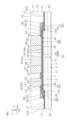
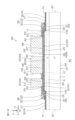
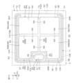
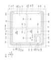
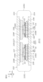
- FIG. 1 is a plan view showing the semiconductor device according to the first embodiment.
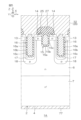
- FIG. FIG. 2 is a cross-sectional view taken along line II-II shown in FIG.
- FIG. 3 is a cross-sectional view taken along line III-III shown in FIG.
- FIG. 4 is an enlarged plan view showing the main part of the inner part of the chip.
- FIG. 5 is a cross-sectional view taken along line V-V shown in FIG.
- FIG. 6 is an enlarged cross-sectional view showing the main part of the periphery of the chip.
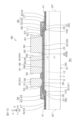
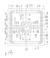
- FIG. 7 is a plan view showing a layout example of gate electrodes and source electrodes.
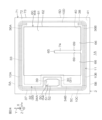
- FIG. 8 is a plan view showing a layout example of the upper insulating film.
- FIG. 9 is a plan view showing the wafer structure used during fabrication.
- FIG. 10 is a cross-sectional view showing the device region shown in FIG. 9.
- FIG. 11A is a cross-sectional view showing an example of a method for manufacturing the semiconductor device shown in FIG. 1.
- FIG. 11B is a cross-sectional view showing a step after FIG. 11A.
- FIG. 11C is a cross-sectional view showing a step after FIG. 11B.
- FIG. 11D is a cross-sectional view showing a step after FIG. 11C.
- FIG. 11E is a cross-sectional view showing a step after FIG. 11D.
- FIG. 11F is a cross-sectional view showing a step after FIG. 11E.
- FIG. 11G is a cross-sectional view showing a step after FIG. 11F.
- FIG. 11A is a cross-sectional view showing an example of a method for manufacturing the semiconductor device shown in FIG. 1.
- FIG. 11B is a cross-sectional view showing a step after FIG. 11A.
- FIG. 11H is a cross-sectional view showing a step after FIG. 11G.
- FIG. 11I is a cross-sectional view showing a step after FIG. 11H.
- FIG. 12 is a plan view showing the semiconductor device according to the second embodiment.
- FIG. 13 is a plan view showing the semiconductor device according to the third embodiment.
- 14 is a cross-sectional view taken along line XIV-XIV shown in FIG. 13.
- FIG. 15 is a circuit diagram showing an electrical configuration of the semiconductor device shown in FIG. 13.
- FIG. FIG. 16 is a plan view showing the semiconductor device according to the fourth embodiment. 17 is a cross-sectional view taken along line XVII-XVII shown in FIG. 16.
- FIG. FIG. 18 is a plan view showing the semiconductor device according to the fifth embodiment.
- FIG. 19 is a plan view showing the semiconductor device according to the sixth embodiment.
- FIG. 20 is a plan view showing the semiconductor device according to the seventh embodiment.
- FIG. 21 is a plan view showing the semiconductor device according to the eighth embodiment.
- 22 is a cross-sectional view taken along line XXII-XXII shown in FIG. 21.
- FIG. 23 is a cross-sectional view showing a modification of the chip applied to each embodiment.
- FIG. 24 is a plan view showing a modification of the gap applied to each embodiment.
- FIG. 25 is a plan view showing a modification of the gap applied to each embodiment.
- FIG. 26 is a cross-sectional view showing a modification of the sealing insulator applied to each embodiment.
- FIG. 27 is a plan view showing a modification of the gate terminal electrode applied to each embodiment.
- FIG. 28 is a plan view showing a package in which the semiconductor devices according to the first to seventh embodiments are mounted.
- FIG. 29 is a plan view showing a package on which a semiconductor device according to the eighth embodiment is mounted;
- FIG. 30 is a perspective view showing a package in which the semiconductor devices according to the first to seventh embodiments and the semiconductor device according to the eighth embodiment are mounted.
- 31 is an exploded perspective view of the package shown in FIG. 30;
- FIG. 32 is a cross-sectional view taken along line XXXII-XXXII shown in FIG. 30.
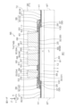
- FIG. 1 is a plan view showing a semiconductor device 1A according to the first embodiment.
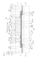
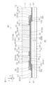
- FIG. 2 is a cross-sectional view taken along line II-II shown in FIG.
- FIG. 3 is a cross-sectional view taken along line III-III shown in FIG.
- FIG. 4 is an enlarged plan view showing the main part of the inner part of the chip 2.
- FIG. 5 is a cross-sectional view taken along line V-V shown in FIG.
- FIG. 6 is an enlarged cross-sectional view showing the essential parts of the periphery of the chip 2.
- FIG. 7 is a plan view showing a layout example of the gate electrode 30 and the source electrode 32.
- FIG. FIG. 8 is a plan view showing a layout example of the upper insulating film 38. As shown in FIG.
- a semiconductor device 1A in this embodiment includes a chip 2 that includes a wide bandgap semiconductor single crystal and is formed in a hexahedral shape (specifically, a rectangular parallelepiped shape). include. That is, the semiconductor device 1A is a "wide bandgap semiconductor device". Chip 2 may also be referred to as a "semiconductor chip” or a "wide bandgap semiconductor chip”.
- a wide bandgap semiconductor is a semiconductor having a bandgap that exceeds the bandgap of Si (silicon). GaN (gallium nitride), SiC (silicon carbide) and C (diamond) are exemplified as wide bandgap semiconductors.
- the chip 2 is, in this embodiment, a "SiC chip" containing a hexagonal SiC single crystal as an example of a wide bandgap semiconductor. That is, the semiconductor device 1A is a "SiC semiconductor device". Hexagonal SiC single crystals have a plurality of polytypes including 2H (Hexagonal)-SiC single crystals, 4H-SiC single crystals, 6H-SiC single crystals and the like. In this form an example is shown in which the chip 2 comprises a 4H—SiC single crystal, but this does not exclude the choice of other polytypes.
- the chip 2 has a first main surface 3 on one side, a second main surface 4 on the other side, and first to fourth side surfaces 5A to 5D connecting the first main surface 3 and the second main surface 4. ing.
- the first main surface 3 and the second main surface 4 are formed in a quadrangular shape when viewed from the normal direction Z (hereinafter simply referred to as "plan view").
- the normal direction Z is also the thickness direction of the chip 2 .
- the first main surface 3 and the second main surface 4 are preferably formed by the c-plane of SiC single crystal.
- the first main surface 3 is formed by the silicon surface of the SiC single crystal
- the second main surface 4 is formed by the carbon surface of the SiC single crystal.
- the first main surface 3 and the second main surface 4 may have an off angle inclined at a predetermined angle in a predetermined off direction with respect to the c-plane.
- the off-direction is preferably the a-axis direction ([11-20] direction) of the SiC single crystal.
- the off angle may exceed 0° and be 10° or less.
- the off angle is preferably 5° or less.
- the second main surface 4 may be a ground surface having grinding marks, or may be a smooth surface having no grinding marks.
- the first side surface 5A and the second side surface 5B extend in the first direction X along the first main surface 3 and face the second direction Y intersecting (specifically, perpendicular to) the first direction X.
- the third side surface 5C and the fourth side surface 5D extend in the second direction Y and face the first direction X.
- the first direction X may be the m-axis direction ([1-100] direction) of the SiC single crystal
- the second direction Y may be the a-axis direction of the SiC single crystal.
- the first direction X may be the a-axis direction of the SiC single crystal
- the second direction Y may be the m-axis direction of the SiC single crystal.
- the first to fourth side surfaces 5A to 5D may be ground surfaces having grinding marks, or may be smooth surfaces having no grinding marks.
- the chip 2 may have a thickness of 5 ⁇ m or more and 250 ⁇ m or less with respect to the normal direction Z.
- the thickness of the chip 2 may be 100 ⁇ m or less.
- the thickness of the chip 2 is preferably 50 ⁇ m or less. It is particularly preferable that the thickness of the chip 2 is 40 ⁇ m or less.
- the first to fourth side surfaces 5A to 5D may have lengths of 0.5 mm or more and 10 mm or less in plan view.
- the length of the first to fourth side surfaces 5A to 5D is preferably 1 mm or more. It is particularly preferable that the lengths of the first to fourth side surfaces 5A to 5D are 2 mm or more. That is, it is preferable that the chip 2 has a plane area of 1 mm square or more (preferably 2 mm square or more) and a thickness of 100 ⁇ m or less (preferably 50 ⁇ m or less) in a cross-sectional view. The lengths of the first to fourth side surfaces 5A to 5D are set in the range of 4 mm or more and 6 mm or less in this embodiment.
- the semiconductor device 1A includes an n-type (first conductivity type) first semiconductor region 6 formed in a region (surface layer portion) on the first main surface 3 side within the chip 2 .
- the first semiconductor region 6 is formed in a layer extending along the first main surface 3 and exposed from the first main surface 3 and the first to fourth side surfaces 5A to 5D.
- the first semiconductor region 6 consists of an epitaxial layer (specifically, a SiC epitaxial layer) in this embodiment.
- the first semiconductor region 6 may have a thickness in the normal direction Z of 1 ⁇ m or more and 50 ⁇ m or less.
- the thickness of the first semiconductor region 6 is preferably 3 ⁇ m or more and 30 ⁇ m or less. It is particularly preferable that the thickness of the first semiconductor region 6 is 5 ⁇ m or more and 25 ⁇ m or less.
- the semiconductor device 1A includes an n-type second semiconductor region 7 formed in a region (surface layer portion) on the second main surface 4 side within the chip 2 .
- the second semiconductor region 7 is formed in a layer extending along the second main surface 4 and exposed from the second main surface 4 and the first to fourth side surfaces 5A to 5D.
- the second semiconductor region 7 has a higher n-type impurity concentration than the first semiconductor region 6 and is electrically connected to the first semiconductor region 6 .
- the second semiconductor region 7 is made of a semiconductor substrate (specifically, a SiC semiconductor substrate) in this embodiment. That is, the chip 2 has a laminated structure including a semiconductor substrate and an epitaxial layer.
- the second semiconductor region 7 may have a thickness of 1 ⁇ m or more and 200 ⁇ m or less with respect to the normal direction Z.
- the thickness of the second semiconductor region 7 is preferably 5 ⁇ m or more and 50 ⁇ m or less. It is particularly preferable that the thickness of the second semiconductor region 7 is 5 ⁇ m or more and 20 ⁇ m or less.
- the thickness of the second semiconductor region 7 is preferably 10 ⁇ m or more. Most preferably, the thickness of the second semiconductor region 7 is less than the thickness of the first semiconductor region 6 .
- the resistance value for example, on-resistance
- the thickness of the second semiconductor region 7 may exceed the thickness of the first semiconductor region 6 .
- the semiconductor device 1A includes an active surface 8 formed on the first main surface 3, an outer surface 9, and first to fourth connection surfaces 10A to 10D (connecting surfaces).
- the active surface 8, the outer surface 9 and the first to fourth connection surfaces 10A to 10D define a mesa portion 11 (plateau) on the first main surface 3.
- the active surface 8 may be called "first surface”
- the outer surface 9 may be called “second surface”
- the first to fourth connection surfaces 10A to 10D may be called “connection surfaces”.
- the active surface 8, the outer surface 9 and the first to fourth connection surfaces 10A-10D (that is, the mesa portion 11) may be regarded as components of the chip 2 (first main surface 3).
- the active surface 8 is formed spaced inwardly from the periphery of the first main surface 3 (first to fourth side surfaces 5A to 5D).
- the active surface 8 has a flat surface extending in the first direction X and the second direction Y. As shown in FIG. In this form, the active surface 8 is formed in a square shape having four sides parallel to the first to fourth side surfaces 5A to 5D in plan view.
- the outer surface 9 is located outside the active surface 8 and recessed from the active surface 8 in the thickness direction of the chip 2 (the second main surface 4 side). Specifically, the outer surface 9 is recessed to a depth less than the thickness of the first semiconductor region 6 so as to expose the first semiconductor region 6 .
- the outer side surface 9 extends in a belt shape along the active surface 8 in a plan view and is formed in an annular shape (specifically, a quadrangular annular shape) surrounding the active surface 8 .
- the outer side surface 9 has flat surfaces extending in the first direction X and the second direction Y and formed substantially parallel to the active surface 8 .
- the outer side surface 9 is continuous with the first to fourth side surfaces 5A to 5D.
- the first to fourth connection surfaces 10A to 10D extend in the normal direction Z and connect the active surface 8 and the outer surface 9.
- the first connection surface 10A is positioned on the first side surface 5A side
- the second connection surface 10B is positioned on the second side surface 5B side
- the third connection surface 10C is positioned on the third side surface 5C side
- the fourth connection surface 10D. is located on the side of the fourth side surface 5D.
- the first connection surface 10A and the second connection surface 10B extend in the first direction X and face the second direction Y.
- the third connection surface 10C and the fourth connection surface 10D extend in the second direction Y and face the first direction X.
- the first to fourth connection surfaces 10A to 10D may extend substantially vertically between the active surface 8 and the outer surface 9 so as to define a quadrangular prism-shaped mesa portion 11.
- the first to fourth connection surfaces 10A to 10D may be inclined downward from the active surface 8 toward the outer surface 9 so that the mesa portion 11 in the shape of a truncated square pyramid is defined.
- semiconductor device 1A includes mesa portion 11 formed in first semiconductor region 6 on first main surface 3 .
- the mesa portion 11 is formed only in the first semiconductor region 6 and not formed in the second semiconductor region 7 .
- a semiconductor device 1A includes a MISFET (Metal Insulator Semiconductor Field Effect Transistor) structure 12 formed on an active surface 8 (first main surface 3). 2 and 3, the MISFET structure 12 is shown simplified by dashed lines. A specific structure of the MISFET structure 12 will be described below with reference to FIGS. 4 and 5. FIG.
- MISFET Metal Insulator Semiconductor Field Effect Transistor
- the MISFET structure 12 includes a p-type (second conductivity type) body region 13 formed on the surface layer of the active surface 8 .
- the body region 13 is formed spaced from the bottom of the first semiconductor region 6 toward the active surface 8 side.
- Body region 13 is formed in a layered shape extending along active surface 8 .
- the body region 13 may be partially exposed from the first to fourth connection surfaces 10A to 10D.
- the MISFET structure 12 includes an n-type source region 14 formed on the surface layer of the body region 13 .
- the source region 14 has an n-type impurity concentration higher than that of the first semiconductor region 6 .
- the source region 14 is formed spaced from the bottom of the body region 13 toward the active surface 8 side.
- the source region 14 is formed in layers extending along the active surface 8 .
- Source region 14 may be exposed from the entire active surface 8 .
- the source region 14 may be exposed from part of the first to fourth connection surfaces 10A to 10D.
- Source region 14 forms a channel in body region 13 with first semiconductor region 6 .
- the MISFET structure 12 includes multiple gate structures 15 formed on the active surface 8 .
- the plurality of gate structures 15 are arranged in the first direction X at intervals in plan view, and are formed in strips extending in the second direction Y, respectively.
- a plurality of gate structures 15 extend through the body region 13 and the source region 14 to reach the first semiconductor region 6 .
- a plurality of gate structures 15 control channel inversion and non-inversion within the body region 13 .
- Each gate structure 15, in this form, includes a gate trench 15a, a gate insulating film 15b and a gate buried electrode 15c.
- a gate trench 15 a is formed in the active surface 8 and defines the walls of the gate structure 15 .
- the gate insulating film 15b covers the walls of the gate trench 15a.
- the gate buried electrode 15c is buried in the gate trench 15a with the gate insulating film 15b interposed therebetween and faces the channel with the gate insulating film 15b interposed therebetween.
- the MISFET structure 12 includes multiple source structures 16 formed on the active surface 8 .
- a plurality of source structures 16 are arranged in regions between a pair of adjacent gate structures 15 on the active surface 8 .
- the plurality of source structures 16 are each formed in a strip shape extending in the second direction Y in plan view.
- a plurality of source structures 16 extend through the body region 13 and the source region 14 to reach the first semiconductor region 6 .
- a plurality of source structures 16 have a depth that exceeds the depth of gate structures 15 .
- the plurality of source structures 16 specifically has a depth approximately equal to the depth of the outer surface 9 .
- Each source structure 16 includes a source trench 16a, a source insulating film 16b and a source buried electrode 16c.
- a source trench 16 a is formed in the active surface 8 and defines the walls of the source structure 16 .
- the source insulating film 16b covers the walls of the source trench 16a.
- the source buried electrode 16c is buried in the source trench 16a with the source insulating film 16b interposed therebetween.
- the MISFET structure 12 includes a plurality of p-type contact regions 17 respectively formed in regions along the plurality of source structures 16 within the chip 2 .
- a plurality of contact regions 17 have a higher p-type impurity concentration than body region 13 .
- Each contact region 17 covers the sidewalls and bottom walls of each source structure 16 and is electrically connected to body region 13 .
- the MISFET structure 12 includes a plurality of p-type well regions 18 respectively formed in regions along the plurality of source structures 16 within the chip 2 .
- Each well region 18 may have a p-type impurity concentration higher than body region 13 and lower than contact region 17 .
- Each well region 18 covers the corresponding source structure 16 with the corresponding contact region 17 interposed therebetween.
- Each well region 18 covers the sidewalls and bottom walls of corresponding source structure 16 and is electrically connected to body region 13 and contact region 17 .
- semiconductor device 1A includes p-type outer contact region 19 formed in the surface layer portion of outer side surface 9 .
- Outer contact region 19 has a p-type impurity concentration higher than that of body region 13 .
- the outer contact region 19 is formed in a band-like shape extending along the active surface 8 and spaced apart from the peripheral edge of the active surface 8 and the peripheral edge of the outer side surface 9 in plan view.
- the outer contact region 19 is formed in a ring shape (specifically, a square ring shape) surrounding the active surface 8 in plan view.
- the outer contact region 19 is formed spaced apart from the bottom of the first semiconductor region 6 to the outer side surface 9 .
- the outer contact region 19 is located on the bottom side of the first semiconductor region 6 with respect to the bottom walls of the plurality of gate structures 15 (source structures 16).
- the semiconductor device 1A includes a p-type outer well region 20 formed in the surface layer portion of the outer side surface 9 .
- the outer well region 20 has a p-type impurity concentration lower than that of the outer contact region 19 .
- the p-type impurity concentration of the outer well region 20 is preferably approximately equal to the p-type impurity concentration of the well region 18 .
- the outer well region 20 is formed in a region between the peripheral edge of the active surface 8 and the outer contact region 19 in plan view, and is formed in a strip shape extending along the active surface 8 .
- the outer well region 20 is formed in an annular shape (specifically, a quadrangular annular shape) surrounding the active surface 8 in plan view.
- the outer well region 20 is formed spaced apart from the bottom of the first semiconductor region 6 to the outer side surface 9 .
- the outer well region 20 may be formed deeper than the outer contact region 19 .
- the outer well region 20 is located on the bottom side of the first semiconductor region 6 with respect to the bottom walls of the plurality of gate structures 15 (source structures 16).
- the outer well region 20 is electrically connected to the outer contact region 19.
- the outer well region 20 extends from the outer contact region 19 side toward the first to fourth connection surfaces 10A to 10D and covers the first to fourth connection surfaces 10A to 10D.
- Outer well region 20 is electrically connected to body region 13 at the surface layer of active surface 8 .
- the semiconductor device 1A has at least one (preferably two or more and twenty or less) p-type field regions 21 formed in a region between the peripheral edge of the outer side surface 9 and the outer contact region 19 in the surface layer portion of the outer side surface 9. including.
- the semiconductor device 1A includes five field regions 21 in this form.
- a plurality of field regions 21 relax the electric field within the chip 2 at the outer surface 9 .
- the number, width, depth, p-type impurity concentration, etc. of the field regions 21 are arbitrary and can take various values according to the electric field to be relaxed.
- the plurality of field regions 21 are arranged at intervals from the outer contact region 19 side to the peripheral edge side of the outer surface 9 .
- the plurality of field regions 21 are formed in strips extending along the active surface 8 in plan view.
- the plurality of field regions 21 are formed in a ring shape (specifically, a square ring shape) surrounding the active surface 8 in plan view.
- the plurality of field regions 21 are each formed as an FLR (Field Limiting Ring) region.
- a plurality of field regions 21 are formed at intervals from the bottom of the first semiconductor region 6 to the outer surface 9 .
- the plurality of field regions 21 are located on the bottom side of the first semiconductor region 6 with respect to the bottom walls of the plurality of gate structures 15 (source structures 16).
- a plurality of field regions 21 may be formed deeper than the outer contact region 19 .
- the innermost field region 21 may be connected to the outer contact region 19 .
- the semiconductor device 1A includes a main surface insulating film 25 covering the first main surface 3.
- Main surface insulating film 25 may include at least one of a silicon oxide film, a silicon nitride film, and a silicon oxynitride film.
- the main surface insulating film 25 has a single layer structure made of a silicon oxide film in this embodiment.
- Main surface insulating film 25 particularly preferably includes a silicon oxide film made of oxide of chip 2 .
- the main surface insulating film 25 covers the active surface 8, the outer surface 9 and the first to fourth connection surfaces 10A to 10D.
- the main surface insulating film 25 continues to the gate insulating film 15b and the source insulating film 16b, and covers the active surface 8 so as to expose the gate buried electrode 15c and the source buried electrode 16c.
- the main surface insulating film 25 covers the outer surface 9 and the first to fourth connection surfaces 10A to 10D so as to cover the outer contact region 19, the outer well region 20 and the plurality of field regions 21. As shown in FIG.
- the main surface insulating film 25 may be continuous with the first to fourth side surfaces 5A to 5D.
- the outer wall of the main surface insulating film 25 may be a ground surface having grinding marks.
- the outer wall of the main surface insulating film 25 may form one ground surface together with the first to fourth side surfaces 5A to 5D.
- the outer wall of the main surface insulating film 25 may be formed with a space inwardly from the peripheral edge of the outer surface 9 to expose the first semiconductor region 6 from the peripheral edge of the outer surface 9 .
- the semiconductor device 1A includes a sidewall structure 26 formed on the main surface insulating film 25 so as to cover at least one of the first to fourth connection surfaces 10A to 10D on the outer surface 9.
- the sidewall structure 26 is formed in an annular shape (square annular shape) surrounding the active surface 8 in plan view.
- the sidewall structure 26 may have a portion overlying the active surface 8 .
- Sidewall structure 26 may comprise an inorganic insulator or polysilicon.
- Sidewall structure 26 may be a sidewall interconnect electrically connected to source structure 16 .
- the semiconductor device 1A includes an interlayer insulating film 27 formed on the main surface insulating film 25 .
- Interlayer insulating film 27 may include at least one of a silicon oxide film, a silicon nitride film, and a silicon oxynitride film.
- the interlayer insulating film 27 has a single-layer structure made of a silicon oxide film in this embodiment.
- the interlayer insulating film 27 covers the active surface 8, the outer side surface 9 and the first to fourth connection surfaces 10A to 10D with the main surface insulating film 25 interposed therebetween. Specifically, the interlayer insulating film 27 covers the active surface 8, the outer side surface 9 and the first to fourth connection surfaces 10A to 10D with the sidewall structure 26 interposed therebetween. The interlayer insulating film 27 covers the MISFET structure 12 on the active surface 8 side, and covers the outer contact region 19, the outer well region 20 and the plurality of field regions 21 on the outer side surface 9 side.
- the interlayer insulating film 27 continues to the first to fourth side surfaces 5A to 5D in this form.
- the outer wall of the interlayer insulating film 27 may be a ground surface having grinding marks.
- the outer wall of the interlayer insulating film 27 may form one ground surface together with the first to fourth side surfaces 5A to 5D.
- the outer wall of the interlayer insulating film 27 may be formed spaced inwardly from the peripheral edge of the outer side surface 9 to expose the first semiconductor region 6 from the peripheral edge portion of the outer side surface 9 .
- the semiconductor device 1A includes a gate electrode 30 arranged on the first main surface 3 (interlayer insulating film 27).
- Gate electrode 30 may be referred to as a “gate main surface electrode”.
- the gate electrode 30 is arranged in the inner part of the first main surface 3 with a space from the peripheral edge of the first main surface 3 .
- a gate electrode 30 is arranged above the active surface 8 in this embodiment.
- the gate electrode 30 is arranged in a region on the periphery of the active surface 8 and close to the central portion of the third connection surface 10C (third side surface 5C).
- the gate electrode 30 is formed in a square shape in plan view.
- the gate electrode 30 may be formed in a polygonal shape other than a square shape, a circular shape, or an elliptical shape in plan view.
- the gate electrode 30 preferably has a plane area of 25% or less of the first main surface 3.
- the planar area of gate electrode 30 may be 10% or less of first main surface 3 .
- the gate electrode 30 may have a thickness of 0.5 ⁇ m or more and 15 ⁇ m or less.
- Gate electrode 30 includes a gate lower conductor layer 31 .
- the gate lower conductor layer 31 may include at least one of a Ti film, a TiN film, a W film, an Al film, a Cu film, an Al alloy film, a Cu alloy film and a conductive polysilicon film.
- the gate lower conductor layer 31 includes a pure Cu film (a Cu film with a purity of 99% or more), a pure Al film (an Al film with a purity of 99% or more), an AlCu alloy film, an AlSi alloy film, and an AlSiCu alloy film. may include at least one of In this embodiment, the gate lower conductor layer 31 has a laminated structure including a Ti film and an Al alloy film (AlSiCu alloy film in this embodiment) laminated in this order from the chip 2 side.
- the semiconductor device 1A includes a source electrode 32 spaced from the gate electrode 30 and arranged on the first main surface 3 (interlayer insulating film 27).
- the source electrode 32 may be referred to as a "source main surface electrode”.
- the source electrode 32 is arranged in the inner part of the first main surface 3 with a space from the periphery of the first main surface 3 .
- a source electrode 32 is arranged on the active surface 8 in this embodiment.
- the source electrode 32 has a body electrode portion 33 and at least one (in this embodiment, a plurality of) extraction electrode portions 34A and 34B.
- the body electrode portion 33 is arranged in a region on the side of the fourth side surface 5D (fourth connection surface 10D) with a gap from the gate electrode 30 in plan view, and faces the gate electrode 30 in the first direction X.
- the body electrode portion 33 is formed in a polygonal shape (specifically, a rectangular shape) having four sides parallel to the first to fourth side surfaces 5A to 5D in plan view.
- the multiple lead electrode portions 34A and 34B include a first lead electrode portion 34A on one side (first side surface 5A side) and a second lead electrode portion 34B on the other side (second side surface 5B side).
- the first extraction electrode portion 34A is extracted from the body electrode portion 33 to a region located on one side (first side surface 5A side) in the second direction Y with respect to the gate electrode 30 in plan view, and extends in the second direction Y to the gate electrode portion 34A. It faces the electrode 30 .
- the second extraction electrode portion 34B is extracted from the body electrode portion 33 to a region located on the other side (the second side surface 5B side) in the second direction Y with respect to the gate electrode 30 in plan view, and extends in the second direction Y to the gate electrode portion 34B. It faces the electrode 30 . That is, the plurality of extraction electrode portions 34A and 34B sandwich the gate electrode 30 from both sides in the second direction Y in plan view.
- the source electrode 32 (body electrode portion 33 and lead-out electrode portions 34A and 34B) penetrates the interlayer insulating film 27 and the main surface insulating film 25 and electrically connects the plurality of source structures 16, the source regions 14 and the plurality of well regions 18. It is connected to the.
- the source electrode 32 may be composed of only the body electrode portion 33 without the lead electrode portions 34A and 34B.
- the source electrode 32 has a planar area that exceeds the planar area of the gate electrode 30 .
- the plane area of the source electrode 32 is preferably 50% or more of the first main surface 3 . It is particularly preferable that the plane area of the source electrode 32 is 75% or more of the first main surface 3 .
- the source electrode 32 includes a source lower conductor layer 35 .
- the source lower conductor layer 35 may include at least one of a Ti film, a TiN film, a W film, an Al film, a Cu film, an Al alloy film, a Cu alloy film and a conductive polysilicon film.
- the source lower conductor layer 35 includes a pure Cu film (a Cu film with a purity of 99% or higher), a pure Al film (an Al film with a purity of 99% or higher), an AlCu alloy film, an AlSi alloy film, and an AlSiCu alloy film. preferably includes at least one of
- the source lower conductor layer 35 has a laminated structure including a Ti film and an Al alloy film (AlSiCu alloy film in this embodiment) laminated in this order from the chip 2 side.
- Source lower conductor layer 35 preferably comprises the same conductive material as gate lower conductor layer 31 .
- the source lower conductor layer 35 (source electrode 32) may have a thickness of 0.5 ⁇ m or more and 15 ⁇ m or less.
- the semiconductor device 1A includes at least one (a plurality in this embodiment) gate wirings 36A and 36B drawn from the gate electrode 30 onto the first main surface 3 (interlayer insulating film 27).
- the plurality of gate wirings 36A, 36B includes the gate lower conductor layer 31, similar to the gate electrode 30. As shown in FIG. A plurality of gate lines 36A, 36B cover the active surface 8 and do not cover the outer surface 9 in this configuration.
- a plurality of gate wirings 36A and 36B are led out to a region between the peripheral edge of the active surface 8 and the source electrode 32 in a plan view, and extend along the source electrode 32 in a strip shape.
- the plurality of gate wirings 36A, 36B specifically includes a first gate wiring 36A and a second gate wiring 36B.
- the first gate wiring 36A is drawn from the gate electrode 30 to a region on the first side surface 5A side in plan view.
- the first gate line 36A has a strip-like portion extending in the second direction Y along the third side surface 5C and a strip-like portion extending in the first direction X along the first side surface 5A.
- the second gate wiring 36B is drawn from the gate electrode 30 to a region on the second side surface 5B side in plan view.
- the second gate line 36B has a strip-like portion extending in the second direction Y along the third side surface 5C and a strip-like portion extending in the first direction X along the second side surface 5B.
- the plurality of gate wirings 36A and 36B intersect (specifically, perpendicularly) both ends of the plurality of gate structures 15 at the periphery of the active surface 8 (first main surface 3).
- the multiple gate wirings 36A and 36B are electrically connected to the multiple gate structures 15 through the interlayer insulating film 27 .
- the plurality of gate wirings 36A and 36B may be directly connected to the plurality of gate structures 15, or may be electrically connected to the plurality of gate structures 15 via a conductor film.
- the semiconductor device 1A includes a source wiring 37 drawn from the source electrode 32 onto the first main surface 3 (interlayer insulating film 27).
- the source line 37 includes a source lower conductor layer 35 as does the source electrode 32 .
- the source wiring 37 is formed in a strip shape extending along the periphery of the active surface 8 in a region closer to the outer surface 9 than the plurality of gate wirings 36A and 36B.
- the source wiring 37 is formed in a ring shape (specifically, a square ring shape) surrounding the gate electrode 30, the source electrode 32 and the plurality of gate wirings 36A and 36B in plan view.
- the source wiring 37 covers the sidewall structure 26 with the interlayer insulating film 27 interposed therebetween, and is drawn out from the active surface 8 side to the outer surface 9 side.
- the source wiring 37 preferably covers the entire sidewall structure 26 over the entire circumference.
- Source line 37 has a portion that penetrates interlayer insulating film 27 and main surface insulating film 25 on the side of outer surface 9 and is connected to outer surface 9 (specifically, outer contact region 19).
- the source wiring 37 may be electrically connected to the sidewall structure 26 through the interlayer insulating film 27 .
- the semiconductor device 1A includes an upper insulating film 38 that selectively covers the gate electrode 30, the source electrode 32, the plurality of gate wirings 36A and 36B, and the source wiring 37.
- the upper insulating film 38 has a gate opening 39 that exposes the inner portion of the gate electrode 30 and covers the peripheral portion of the gate electrode 30 over the entire circumference.
- the gate opening 39 is formed in a square shape in plan view.
- the upper insulating film 38 has a source opening 40 that exposes the inner part of the source electrode 32 in plan view, and covers the peripheral edge of the source electrode 32 over the entire circumference.
- the source opening 40 is formed in a polygonal shape along the source electrode 32 in plan view.
- the upper insulating film 38 covers the entire area of the plurality of gate wirings 36A and 36B and the entire area of the source wiring 37 .
- the upper insulating film 38 covers the sidewall structure 26 with the interlayer insulating film 27 interposed therebetween, and extends from the active surface 8 side to the outer surface 9 side.
- the upper insulating film 38 is formed spaced inwardly from the periphery of the outer side surface 9 (first to fourth side surfaces 5A to 5D) and covers the outer contact region 19, the outer well region 20 and the plurality of field regions 21. are doing.
- the upper insulating film 38 partitions the dicing streets 41 with the periphery of the outer side surface 9 .
- the dicing street 41 is formed in a strip shape extending along the peripheral edges (first to fourth side surfaces 5A to 5D) of the outer side surface 9 in plan view.
- the dicing street 41 is formed in an annular shape (specifically, a quadrangular annular shape) surrounding the inner portion (active surface 8) of the first main surface 3 in plan view.
- the dicing street 41 exposes the interlayer insulating film 27 in this form.
- the dicing streets 41 may expose the outer surface 9 .
- the dicing street 41 may have a width of 1 ⁇ m or more and 200 ⁇ m or less.
- the width of the dicing street 41 is the width in the direction perpendicular to the extending direction of the dicing street 41 .
- the width of the dicing street 41 is preferably 5 ⁇ m or more and 50 ⁇ m or less.
- the upper insulating film 38 preferably has a thickness exceeding the thickness of the gate electrode 30 and the thickness of the source electrode 32 .
- the thickness of the upper insulating film 38 is preferably less than the thickness of the chip 2 .
- the thickness of the upper insulating film 38 may be 3 ⁇ m or more and 35 ⁇ m or less.
- the thickness of the upper insulating film 38 is preferably 25 ⁇ m or less.
- the upper insulating film 38 has a laminated structure including an inorganic insulating film 42 and an organic insulating film 43 laminated in this order from the chip 2 side.
- the upper insulating film 38 may include at least one of the inorganic insulating film 42 and the organic insulating film 43, and does not necessarily include the inorganic insulating film 42 and the organic insulating film 43 at the same time.
- the inorganic insulating film 42 selectively covers the gate electrode 30, the source electrode 32, the plurality of gate wirings 36A and 36B, and the source wiring 37, and partially covers the gate opening 39, the source opening 40, and the dicing street 41. Some are partitioned.
- the inorganic insulating film 42 may include at least one of a silicon oxide film, a silicon nitride film and a silicon oxynitride film.
- the inorganic insulating film 42 preferably contains an insulating material different from that of the interlayer insulating film 27 .
- the inorganic insulating film 42 preferably contains a silicon nitride film.
- the inorganic insulating film 42 preferably has a thickness less than the thickness of the interlayer insulating film 27 .
- the inorganic insulating film 42 may have a thickness of 0.1 ⁇ m or more and 5 ⁇ m or less.
- the organic insulating film 43 selectively covers the inorganic insulating film 42 and partitions part of the gate opening 39 , part of the source opening 40 and part of the dicing street 41 . Specifically, the organic insulating film 43 partially exposes the inorganic insulating film 42 on the wall surface of the gate opening 39 . Also, the organic insulating film 43 partially exposes the inorganic insulating film 42 on the wall surface of the source opening 40 . Further, the organic insulating film 43 partially exposes the inorganic insulating film 42 on the wall surface of the dicing street 41 .
- the organic insulating film 43 may cover the inorganic insulating film 42 so that the inorganic insulating film 42 is not exposed from the wall surface of the gate opening 39 .
- the organic insulating film 43 may cover the inorganic insulating film 42 so that the inorganic insulating film 42 is not exposed from the wall surface of the source opening 40 .
- the organic insulating film 43 may cover the inorganic insulating film 42 so that the inorganic insulating film 42 is not exposed from the wall surfaces of the dicing streets 41 . In these cases, the organic insulating film 43 may cover the entire inorganic insulating film 42 .
- the organic insulating film 43 is preferably made of a resin film other than thermosetting resin.
- the organic insulating film 43 may be made of translucent resin or transparent resin.
- the organic insulating film 43 may be made of a negative type or positive type photosensitive resin film.
- the organic insulating film 43 is preferably made of a polyimide film, a polyamide film, or a polybenzoxazole film.
- the organic insulating film 43 includes a polybenzoxazole film in this form.
- the organic insulating film 43 preferably has a thickness exceeding the thickness of the inorganic insulating film 42 .
- the thickness of the organic insulating film 43 preferably exceeds the thickness of the interlayer insulating film 27 . It is particularly preferable that the thickness of the organic insulating film 43 exceeds the thickness of the gate electrode 30 and the thickness of the source electrode 32 .
- the thickness of the organic insulating film 43 may be 3 ⁇ m or more and 30 ⁇ m or less.
- the thickness of the organic insulating film 43 is preferably 20 ⁇ m or less.
- the semiconductor device 1A includes a gate terminal electrode 50 arranged on the gate electrode 30 .
- the gate terminal electrode 50 is erected in a pillar shape on a portion of the gate electrode 30 exposed from the gate opening 39 .
- the gate terminal electrode 50 has an area smaller than that of the gate electrode 30 in a plan view, and is arranged above the inner portion of the gate electrode 30 with a gap from the periphery of the gate electrode 30 .
- the gate terminal electrode 50 has a gate terminal surface 51 and gate terminal sidewalls 52 .
- Gate terminal surface 51 extends flat along first main surface 3 .
- the gate terminal surface 51 may be a ground surface having grinding marks.
- the gate terminal side wall 52 is located on the upper insulating film 38 (more specifically, the organic insulating film 43) in this embodiment.
- the gate terminal electrode 50 includes portions in contact with the inorganic insulating film 42 and the organic insulating film 43 .
- the gate terminal sidewall 52 extends substantially vertically in the normal direction Z. As shown in FIG. "Substantially vertical” also includes a form extending in the stacking direction while curving (meandering).
- Gate terminal sidewall 52 includes a portion facing gate electrode 30 with upper insulating film 38 interposed therebetween.
- the gate terminal side walls 52 are preferably smooth surfaces without grinding marks.
- the gate terminal electrode 50 has a first projecting portion 53 projecting outward from the lower end portion of the gate terminal side wall 52 .
- the first projecting portion 53 is formed in a region closer to the upper insulating film 38 (organic insulating film 43 ) than the intermediate portion of the gate terminal side wall 52 .
- the first projecting portion 53 extends along the outer surface of the upper insulating film 38 in a cross-sectional view, and is formed in a tapered shape in which the thickness gradually decreases from the gate terminal side wall 52 toward the tip portion.
- the first projecting portion 53 has a sharp tip that forms an acute angle.
- the gate terminal electrode 50 without the first projecting portion 53 may be formed.
- the gate terminal electrode 50 preferably has a thickness exceeding the thickness of the gate electrode 30 .
- the thickness of gate terminal electrode 50 is defined by the distance between gate electrode 30 and gate terminal surface 51 . It is particularly preferable that the thickness of the gate terminal electrode 50 exceeds the thickness of the upper insulating film 38 .
- the thickness of the gate terminal electrode 50 exceeds the thickness of the chip 2 in this embodiment. Of course, the thickness of the gate terminal electrode 50 may be less than the thickness of the chip 2 .
- the thickness of the gate terminal electrode 50 may be 10 ⁇ m or more and 300 ⁇ m or less.
- the thickness of the gate terminal electrode 50 is preferably 30 ⁇ m or more. It is particularly preferable that the thickness of the gate terminal electrode 50 is 80 ⁇ m or more and 200 ⁇ m or less.
- the planar area of the gate terminal electrode 50 is adjusted according to the planar area of the first main surface 3 .
- the planar area of the gate terminal electrode 50 is defined by the planar area of the gate terminal surface 51 .
- the planar area of gate terminal electrode 50 is preferably 25% or less of first main surface 3 .
- the planar area of the gate terminal electrode 50 may be 10% or less of the first main surface 3 .
- the plane area of the gate terminal electrode 50 may be 0.4 mm square or more.
- Gate terminal electrode 50 may be formed in a polygonal shape (for example, rectangular shape) having a plane area of 0.4 mm ⁇ 0.7 mm or more.
- the gate terminal electrode 50 is formed in a polygonal shape (quadrangular shape with four rectangular notched corners) having four sides parallel to the first to fourth side surfaces 5A to 5D in plan view.
- the gate terminal electrode 50 may be formed in a rectangular shape, a polygonal shape other than a rectangular shape, a circular shape, or an elliptical shape in plan view.
- the gate terminal electrode 50 includes a gate conductor layer 54 covering the gate electrode 30 .
- the gate conductor layer 54 covers the gate electrode 30 and the upper insulating film 38 within the gate opening 39 in this embodiment.
- the gate conductor layer 54 uniformly covers the gate electrode 30 and the upper insulating film 38 . Therefore, the gate terminal electrode 50 does not include a gap penetrating through the gate conductor layer 54 in the thickness direction.
- the gate conductor layer 54 has a laminated structure including a first gate conductor film 55 and a second gate conductor film 56 laminated in this order from the gate electrode 30 side.
- the first gate conductor film 55 may contain a Ti-based metal film.
- the first gate conductor film 55 may have a single layer structure made of a Ti film or a TiN film.
- the first gate conductor film 55 may have a laminated structure including a Ti film and a TiN film laminated in any order.
- the first gate conductor film 55 has a thickness less than the thickness of the gate electrode 30 .
- the first gate conductor film 55 covers the gate electrode 30 in the form of a film in the gate opening 39 and is pulled out on the upper insulating film 38 in the form of a film.
- the first gate conductor film 55 forms part of the first projecting portion 53 .
- the first gate conductor film 55 is not necessarily formed and may be removed.
- the second gate conductor film 56 forms the main body of the gate terminal electrode 50 .
- the second gate conductor film 56 may contain a Cu-based metal film.
- the Cu-based metal film may be a pure Cu film (a Cu film with a purity of 99% or more) or a Cu alloy film.
- the second gate conductor film 56 includes a pure Cu plating film in this embodiment.
- the second gate conductor film 56 preferably has a thickness exceeding the thickness of the gate electrode 30 . It is particularly preferable that the thickness of the second gate conductor film 56 exceeds the thickness of the upper insulating film 38 . The thickness of the second gate conductor film 56 exceeds the thickness of the chip 2 in this embodiment.
- the second gate conductor film 56 covers the gate electrode 30 in the gate opening 39 with the first gate conductor film 55 interposed therebetween, and is pulled out in the form of a film onto the upper insulating film 38 with the first gate conductor film 55 interposed therebetween. ing.
- the second gate conductor film 56 forms part of the first projecting portion 53 . That is, the first projecting portion 53 has a laminated structure including the first gate conductor film 55 and the second gate conductor film 56 .
- the second gate conductor film 56 preferably has a thickness exceeding the thickness of the first gate conductor film 55 within the first projecting portion 53 .
- the semiconductor device 1A includes a source terminal electrode 60 arranged on the source electrode 32 .
- the source terminal electrode 60 is erected in a columnar shape on a portion of the source electrode 32 exposed from the source opening 40 .
- the source terminal electrode 60 may have an area smaller than the area of the source electrode 32 in a plan view, and may be arranged above the inner portion of the source electrode 32 with a gap from the periphery of the source electrode 32 .
- the source terminal electrode 60 is formed in a polygonal shape (quadrangular in this form) having four sides parallel to the first to fourth side surfaces 5A to 5D in plan view.
- the source terminal electrode 60 has a source terminal surface 61 and source terminal sidewalls 62 .
- the source terminal surface 61 extends flat along the first main surface 3 .
- the source terminal surface 61 may be a ground surface having grinding marks.
- the source terminal sidewall 62 is located on the upper insulating film 38 (specifically, the organic insulating film 43) in this embodiment.
- the source terminal electrode 60 includes portions in contact with the inorganic insulating film 42 and the organic insulating film 43 .
- the source terminal sidewall 62 extends substantially vertically in the normal direction Z. As shown in FIG. "Substantially vertical” also includes a form extending in the stacking direction while curving (meandering).
- Source terminal sidewall 62 includes a portion facing source electrode 32 with upper insulating film 38 interposed therebetween.
- the source terminal sidewall 62 preferably has a smooth surface without grinding marks.
- the source terminal electrode 60 has a second projecting portion 63 projecting outward from the lower end portion of the source terminal side wall 62 in this embodiment.
- the second projecting portion 63 is formed in a region closer to the upper insulating film 38 (organic insulating film 43 ) than the intermediate portion of the source terminal side wall 62 .
- the second projecting portion 63 extends along the outer surface of the upper insulating film 38 in a cross-sectional view, and is formed in a tapered shape in which the thickness gradually decreases from the source terminal side wall 62 toward the tip portion.
- the second projecting portion 63 has a sharp tip that forms an acute angle.
- the source terminal electrode 60 without the second projecting portion 63 may be formed.
- the source terminal electrode 60 preferably has a thickness exceeding the thickness of the source electrode 32 .
- the thickness of source terminal electrode 60 is defined by the distance between source electrode 32 and source terminal surface 61 . It is particularly preferable that the thickness of the source terminal electrode 60 exceeds the thickness of the upper insulating film 38 . The thickness of the source terminal electrode 60 exceeds the thickness of the chip 2 in this embodiment.
- the thickness of the source terminal electrode 60 may be less than the thickness of the chip 2.
- the thickness of the source terminal electrode 60 may be 10 ⁇ m or more and 300 ⁇ m or less.
- the thickness of the source terminal electrode 60 is preferably 30 ⁇ m or more. It is particularly preferable that the thickness of the source terminal electrode 60 is 80 ⁇ m or more and 200 ⁇ m or less.
- the thickness of the source terminal electrode 60 is approximately equal to the thickness of the gate terminal electrode 50 .
- the source terminal electrode 60 includes a source conductor layer 64 , at least one (plurality in this embodiment) source gap portion 65 and at least one (plurality in this embodiment) source terminal portion 66 .
- the source conductor layer 64 covers the source electrode 32 and the upper insulating film 38 within the source opening 40 in this embodiment.
- the source conductor layer 64 has a laminated structure including a first source conductor film 67 and a second source conductor film 68 laminated in this order from the source electrode 32 side.
- the first source conductor film 67 may contain a Ti-based metal film.
- the first source conductor film 67 may have a single layer structure made of a Ti film or a TiN film.
- the first source conductor film 67 may have a laminated structure including a Ti film and a TiN film laminated in any order.
- the first source conductor film 67 is preferably made of the same conductive material as the first gate conductor film 55 .
- the first source conductor film 67 has a thickness less than the thickness of the source electrode 32 .
- the first source conductor film 67 covers the source electrode 32 in the form of a film in the source opening 40 and is pulled out on the upper insulating film 38 in the form of a film.
- the first source conductor film 67 forms part of the second projecting portion 63 .
- the thickness of the first source conductor film 67 is approximately equal to the thickness of the first gate conductor film 55 .
- the first source conductor film 67 does not necessarily have to be formed and may be removed.
- the second source conductor film 68 forms the main body of the source terminal electrode 60 .
- the second source conductor film 68 may contain a Cu-based metal film.
- the Cu-based metal film may be a pure Cu film (a Cu film with a purity of 99% or more) or a Cu alloy film.
- the second source conductor film 68 includes a pure Cu plating film in this embodiment.
- the second source conductor film 68 is preferably made of the same conductive material as the second gate conductor film 56 .
- the second source conductor film 68 preferably has a thickness exceeding the thickness of the source electrode 32 . It is particularly preferable that the thickness of the second source conductor film 68 exceeds the thickness of the upper insulating film 38 . The thickness of the second source conductor film 68 exceeds the thickness of the chip 2 in this form. The thickness of the second source conductor film 68 is approximately equal to the thickness of the second gate conductor film 56 .
- the second source conductor film 68 covers the source electrode 32 in the source opening 40 with the first source conductor film 67 interposed therebetween, and is pulled out in the form of a film onto the upper insulating film 38 with the first source conductor film 67 interposed therebetween. ing.
- the second source conductor film 68 forms part of the second projecting portion 63 . That is, the second projecting portion 63 has a laminated structure including the first source conductor film 67 and the second source conductor film 68 .
- the second source conductor film 68 preferably has a thickness exceeding the thickness of the first source conductor film 67 within the second protruding portion 63 .
- the source gap portion 65 penetrates the source conductor layer 64 in a cross-sectional view, and partitions the source conductor layer 64 into a plurality of portions (regions).
- the source gap 65 is formed at a position overlapping with the source electrode 32 to expose a portion of the source electrode 32 .
- the source gap 65 also exposes a portion of the upper insulating film 38 in this form.
- Source gap 65 in this form, includes a first source gap 65A and a second source gap 65B extending in different directions.
- the first source gap portion 65A is formed in a strip shape extending in the first direction X in plan view, and divides the source conductor layer 64 in the second direction Y. In this form, the first source gap portion 65A crosses the central portion of the source conductor layer 64 in the first direction X in plan view.
- the second source gap portion 65B is formed in a strip shape extending in the second direction Y so as to cross the first source gap portion 65A in plan view, and divides the source conductor layer 64 in the first direction X. As shown in FIG.
- the second source gap portion 65B crosses the central portion of the source conductor layer 64 in the second direction Y in plan view. That is, the second source gap 65B intersects the first source gap 65A at the central portion of the source conductor layer 64. As shown in FIG. The intersecting portion of the first source gap portion 65A and the second source gap portion 65B faces the gate terminal electrode 50 in the first direction X in plan view.
- the first source gap portion 65A may cross the central portion of the first main surface 3 (chip 2) in the first direction X in plan view.
- the second source gap portion 65B may cross the central portion of the first main surface 3 (chip 2) in the second direction Y in plan view.
- the first source gap portion 65A may be formed so as to be shifted in the second direction Y from the central portion of the source conductor layer 64 .
- the second source gap portion 65B may be formed so as to be shifted in the first direction X from the central portion of the source conductor layer 64 .
- the source gap portion 65 does not necessarily include both the first source gap portion 65A and the second source gap portion 65B at the same time, and includes only one of the first source gap portion 65A and the second source gap portion 65B. You can
- the multiple source terminal portions 66 are composed of multiple portions partitioned by the source gap portions 65 in the source conductor layer 64 . That is, in this form, four source terminal portions 66 are partitioned by the first source gap portion 65A and the second source gap portion 65B.
- the plurality of source terminal portions 66 are each fixed at the same potential as the source electrode 32 . That is, the source terminal electrode 60 is configured such that a source potential (single potential) is applied to one source electrode 32 via a plurality of source terminal portions 66 .
- the plurality of source terminal portions 66 are arranged on the body electrode portion 33 of the source electrode 32 and are not arranged on the extraction electrode portions 34A and 34B of the source electrode 32. Thereby, the facing area between the gate terminal electrode 50 and the source terminal portion 66 is reduced.
- Such a structure reduces the risk of shorting between the gate terminal electrode 50 and the source terminal portion 66 when a conductive adhesive such as solder or metal paste is attached to the gate terminal electrode 50 and the source terminal portion 66. is valid.
- a conductive joining member such as a conductive plate or a conductive wire (eg, bonding wire) may be connected to the gate terminal electrode 50 and the source terminal portion 66 . In this case, the risk of short-circuiting between the conductive joint member on the gate terminal electrode 50 side and the conductive joint member on the source terminal portion 66 side can be reduced.
- the plurality of source terminal portions 66 each have source gap sidewalls 69 partitioned by the source gap portions 65 .
- the source gap sidewall 69 preferably has a smooth surface without grinding marks.
- the plurality of source terminal portions 66 each have a second projecting portion 63 at the lower end portion of the source gap side wall 69 in this embodiment. The second projecting portion 63 on the side of the source gap sidewall 69 is positioned above the source electrode 32 .
- each source terminal portion 66 is adjusted according to the plane area of the first main surface 3 .
- the plane area of each source terminal portion 66 is defined by the plane area of the portion of source terminal surface 61 defined by source terminal sidewall 62 and source gap sidewall 69 .
- the total planar area of the plurality of source terminal portions 66 preferably exceeds the planar area of the gate terminal electrode 50 .
- the plane area of each source terminal portion 66 is preferably equal to or greater than the plane area of the gate terminal electrode 50 . It is particularly preferable that the plane area of each source terminal portion 66 exceeds the plane area of the gate terminal electrode 50 .
- the total plane area of the plurality of source terminal portions 66 is preferably 50% or more of the first main surface 3 . It is particularly preferable that the total plane area of the plurality of source terminal portions 66 is 75% or more of the first main surface 3 .
- each source terminal portion 66 is preferably 0.8 mm square or more. In this case, it is particularly preferable that the plane area of each source terminal portion 66 is 1 mm square or more.
- Each source terminal portion 66 may be formed in a polygonal shape having a plane area of 1 mm ⁇ 1.4 mm or more.
- Each source terminal portion 66 is formed in a square shape having four sides parallel to the first to fourth side surfaces 5A to 5D in plan view.
- each source terminal portion 66 may be formed in a polygonal shape other than a square shape, a circular shape, or an elliptical shape in plan view.
- the semiconductor device 1A includes a sealing insulator 71 that covers the first main surface 3.
- the sealing insulator 71 covers the periphery of the gate terminal electrode 50 and the periphery of the source terminal electrode 60 so as to expose a portion of the gate terminal electrode 50 and a portion of the source terminal electrode 60 on the first main surface 3 . are doing.
- the encapsulating insulator 71 covers the active surface 8, the outer surface 9 and the first to fourth connection surfaces 10A to 10D so as to expose the gate terminal electrode 50 and the source terminal electrode 60. As shown in FIG.
- the encapsulation insulator 71 exposes the gate terminal surface 51 and the source terminal surface 61 and covers the gate terminal sidewalls 52 and the source terminal sidewalls 62 .
- the sealing insulator 71 covers the first projecting portion 53 of the gate terminal electrode 50 and faces the upper insulating film 38 with the first projecting portion 53 interposed therebetween.
- the sealing insulator 71 prevents the gate terminal electrode 50 from coming off.
- the sealing insulator 71 covers the second projecting portion 63 of the source terminal electrode 60 and faces the upper insulating film 38 with the second projecting portion 63 interposed therebetween.
- the sealing insulator 71 prevents the source terminal electrode 60 from coming off.
- the sealing insulator 71 covers the dicing street 41 at the periphery of the outer surface 9 .
- the sealing insulator 71 directly covers the interlayer insulating film 27 at the dicing street 41 in this embodiment.
- the sealing insulator 71 directly covers the chip 2 and the main surface insulating film 25 on the dicing street 41.
- the sealing insulator 71 has an insulating main surface 72 and insulating side walls 73 .
- the insulating main surface 72 extends flat along the first main surface 3 .
- Insulating main surface 72 forms one flat surface with gate terminal surface 51 and source terminal surface 61 .
- the insulating main surface 72 may be a ground surface having grinding marks. In this case, the insulating main surface 72 preferably forms one ground surface together with the gate terminal surface 51 and the source terminal surface 61 .
- the insulating side wall 73 extends from the periphery of the insulating main surface 72 toward the chip 2 and forms one flat surface together with the first to fourth side surfaces 5A to 5D.
- the insulating side wall 73 is formed substantially perpendicular to the insulating main surface 72 .
- the angle formed between insulating side wall 73 and insulating main surface 72 may be 88° or more and 92° or less.
- the insulating side wall 73 may consist of a ground surface with grinding marks.
- the insulating sidewall 73 may form one grinding surface with the first to fourth side surfaces 5A to 5D.
- the encapsulating insulator 71 preferably has a thickness exceeding the thickness of the gate electrode 30 and the thickness of the source electrode 32 . It is particularly preferable that the thickness of the sealing insulator 71 exceeds the thickness of the upper insulating film 38 . The thickness of the encapsulation insulator 71 exceeds the thickness of the chip 2 in this embodiment. Of course, the thickness of the encapsulating insulator 71 may be less than the thickness of the chip 2 . The thickness of the sealing insulator 71 may be 10 ⁇ m or more and 300 ⁇ m or less. The thickness of the sealing insulator 71 is preferably 30 ⁇ m or more.
- the thickness of the sealing insulator 71 is 80 ⁇ m or more and 200 ⁇ m or less.
- the thickness of encapsulating insulator 71 is approximately equal to the thickness of gate terminal electrode 50 and the thickness of source terminal electrode 60 .
- the sealing insulator 71 contains a matrix resin, multiple fillers, and multiple flexible particles (flexible agents).
- the sealing insulator 71 is configured such that its mechanical strength is adjusted by the matrix resin, multiple fillers, and multiple flexible particles.
- the sealing insulator 71 only needs to contain a matrix resin, and the presence or absence of fillers and flexible particles is optional.
- the sealing insulator 71 may contain a coloring material such as carbon black for coloring the matrix resin.
- the matrix resin is preferably made of a thermosetting resin.
- the matrix resin may contain at least one of epoxy resin, phenolic resin, and polyimide resin, which are examples of thermosetting resins.
- the matrix resin, in this form, contains an epoxy resin.
- the plurality of fillers are composed of one or both of spherical objects made of insulators and amorphous objects made of insulators, and are added to the matrix resin.
- Amorphous objects have random shapes other than spheres, such as grains, fragments, and crushed pieces.
- the amorphous object may have corners.
- the plurality of fillers are each composed of a spherical object from the viewpoint of suppressing damage due to filler attack.
- the plurality of fillers may contain at least one of ceramics, oxides and nitrides.
- the plurality of fillers in this form, are each composed of silicon oxide particles (silica particles).
- a plurality of fillers may each have a particle size of 1 nm or more and 100 ⁇ m or less.
- the particle size of the plurality of fillers is preferably 50 ⁇ m or less.
- the sealing insulator 71 preferably contains a plurality of fillers with different particle sizes.
- the plurality of fillers may include a plurality of small-diameter fillers, a plurality of medium-diameter fillers, and a plurality of large-diameter fillers.
- the plurality of fillers are preferably added to the matrix resin at a content rate (density) in the order of small-diameter filler, medium-diameter filler, and large-diameter filler.
- the small-diameter filler may have a thickness less than the thickness of the source electrode 32 (the thickness of the gate electrode 30).
- the particle size of the small-diameter filler may be 1 nm or more and 1 ⁇ m or less.
- the medium-diameter filler may have a thickness exceeding the thickness of the source electrode 32 and equal to or less than the thickness of the upper insulating film 38 .
- the particle diameter of the medium-diameter filler may be 1 ⁇ m or more and 20 ⁇ m or less.
- the large-diameter filler may have a thickness exceeding the thickness of the upper insulating film 38 .
- the plurality of fillers includes at least one large diameter filler that exceeds any one of the thickness of the first semiconductor region 6 (epitaxial layer), the thickness of the second semiconductor region 7 (substrate) and the thickness of the chip 2. good too.
- the particle size of the large-diameter filler may be 20 ⁇ m or more and 100 ⁇ m or less.
- the particle size of the large-diameter filler is preferably 50 ⁇ m or less.
- the average particle size of the plurality of fillers may be 1 ⁇ m or more and 10 ⁇ m or less.
- the average particle size of the plurality of fillers is preferably 4 ⁇ m or more and 8 ⁇ m or less.
- the plurality of fillers need not contain all of the small-diameter fillers, medium-diameter fillers and large-diameter fillers at the same time, and may be composed of either one or both of the small-diameter fillers and the medium-diameter fillers.
- the maximum particle size of the plurality of fillers (medium-sized fillers) may be 10 ⁇ m or less.
- the encapsulation insulator 71 may include a plurality of filler fragments having broken particle shapes at the surface of the insulating main surface 72 and the surface of the insulating sidewalls 73 .
- the plurality of filler pieces may each be formed of a portion of the small-diameter filler, a portion of the medium-diameter filler, and a portion of the large-diameter filler.
- the plurality of filler pieces located on the insulating main surface 72 side have broken portions formed along the insulating main surface 72 so as to face the insulating main surface 72 .
- a plurality of filler pieces located on the side of the insulating sidewall 73 have broken portions formed along the insulating sidewall 73 so as to face the insulating sidewall 73 .
- the broken portions of the plurality of filler pieces may be exposed from the insulating main surface 72 and the insulating sidewalls 73, or may be partially or wholly covered with the matrix resin. Since the plurality of filler pieces are located on the surface layers of the insulating main surface 72 and the insulating side walls 73, they do not affect the structures on the chip 2 side.
- a plurality of flexible particles are added to the matrix resin.
- the plurality of flexible particles may include at least one of silicon-based flexible particles, acrylic-based flexible particles, and butadiene-based flexible particles.
- the encapsulating insulator 71 preferably contains silicon-based flexing particles.
- the plurality of flexing particles have an average particle size less than the average particle size of the plurality of fillers.
- the average particle size of the plurality of flexible particles is preferably 1 nm or more and 1 ⁇ m or less.
- the maximum particle size of the plurality of flexible particles is preferably 1 ⁇ m or less.
- the plurality of flexible particles are added to the matrix resin so that the ratio of the total cross-sectional area per unit cross-sectional area is 0.1% or more and 10% or less.
- the plurality of flexible particles are added to the matrix resin at a content in the range of 0.1% by weight to 10% by weight.
- the average particle size and content of the plurality of flexible particles are appropriately adjusted according to the elastic modulus to be imparted to the sealing insulator 71 during and/or after manufacturing.
- the semiconductor device 1A includes gap insulators 74 embedded in the source gaps 65 so as to expose a portion of the source terminal electrode 60 (a portion of the plurality of source terminal portions 66).
- the gap insulator 74 is embedded in the first source gap 65A and the second source gap 65B in this form. That is, the gap insulator 74, in this form, includes a first gap insulator 74A and a second gap insulator 74B.
- the first gap insulator 74A is embedded in the first source gap 65A and extends in the first direction X along the first source gap 65A.
- the second gap insulator 74B is embedded in the second source gap 65B and extends in the second direction Y along the second source gap 65B.
- the gap insulator 74 covers the source electrode 32 in a grid pattern (cross pattern) in plan view.
- the gap insulator 74 covers the source gap side walls 69 of the plurality of source terminal parts 66 in the first source gap part 65A and the second source gap part 65B. That is, the gap insulator 74 partitions the plurality of source terminal portions 66 within the source gap portion 65 . In this form, the gap insulator 74 physically separates the plurality of source terminal portions 66 above the source electrode 32 while keeping the plurality of source terminal portions 66 fixed at the same potential as the source electrode 32 . are doing. In other words, the interstitial insulator 74 allows vertical current transfer between the plurality of source terminal portions 66 and the source electrodes 32 and restricts lateral current transfer between the plurality of source terminal portions 66 . It is configured.
- the gap insulator 74 has a portion that directly covers the source electrode 32 in the source gap 65 in this form.
- the gap insulator 74 covers the second projecting portion 63 in the source gap portion 65 and covers the source electrode 32 with the second projecting portion 63 interposed therebetween.
- the gap insulator 74 prevents the source terminal portion 66 from coming off.
- the gap insulator 74 has a portion that directly covers the upper insulating film 38 in the source gap portion 65 in this embodiment.
- Gap insulator 74 is connected to encapsulation insulator 71 outside source gap 65 .
- the gap insulator 74 consists of part of the sealing insulator 71 in this form.
- the gap insulator 74 has an insulating main surface 72 that continues to the gate terminal surface 51 and the source terminal surface 61 .
- the gap insulator 74 also includes a thermosetting resin, a plurality of fillers and a plurality of flexing particles.
- the gap insulator 74 may be made of a different insulating material than the sealing insulator 71 .
- the semiconductor device 1A includes a drain electrode 77 (second main surface electrode) that covers the second main surface 4 .
- Drain electrode 77 is electrically connected to second main surface 4 .
- Drain electrode 77 forms ohmic contact with second semiconductor region 7 exposed from second main surface 4 .
- the drain electrode 77 may cover the entire second main surface 4 so as to be continuous with the periphery of the chip 2 (first to fourth side surfaces 5A to 5D).
- the drain electrode 77 may cover the second main surface 4 with a space inward from the periphery of the chip 2 .
- the drain electrode 77 is configured such that a drain-source voltage of 500 V or more and 3000 V or less is applied between the source terminal electrode 60 (the plurality of source terminal portions 66). That is, the chip 2 is formed so that a voltage of 500 V or more and 3000 V or less is applied between the first principal surface 3 and the second principal surface 4 .
- the semiconductor device 1A includes the chip 2, the source electrode 32 (main surface electrode), and the source terminal electrode 60.
- Chip 2 has a first main surface 3 .
- the source electrode 32 is arranged on the first main surface 3 .
- the source terminal electrode 60 is arranged on the source electrode 32 and fixed to the same potential as the source electrode 32 .
- Source terminal electrode 60 includes source conductor layer 64 and source gap 65 .
- the source conductor layer 64 covers the source electrode 32 .
- the source gap portion 65 penetrates the source conductor layer 64 in the thickness direction in a cross-sectional view.
- the volume of the source terminal electrode 60 is reduced by the source gap 65, and the stress caused by the source terminal electrode 60 is reduced.
- the source gap portion 65 is also effective in blocking the stress continuously generated in the width direction of the source terminal electrode 60 . As a result, it is possible to suppress variations in electrical characteristics and shape defects caused by the stress of the source terminal electrode 60 . Therefore, it is possible to provide the semiconductor device 1A with improved reliability.
- the semiconductor device 1A preferably includes a gap insulator 74 embedded in the source gap portion 65 .
- the gap insulator 74 can protect the source electrode 32 and the source terminal electrode 60 from external forces and moisture (moisture). Therefore, reliability can be improved.
- the semiconductor device 1A preferably includes a sealing insulator 71 that covers the periphery of the source terminal electrode 60 on the first main surface 3 so that a portion of the source terminal electrode 60 is exposed.
- the sealing insulator 71 can protect the object to be sealed from external force and moisture.
- the object to be sealed can be protected from damage (including peeling) caused by external force and deterioration (including corrosion) caused by humidity. This can suppress shape defects and variations in electrical characteristics. Therefore, reliability can be improved.
- the gap insulator 74 preferably consists of part of the sealing insulator 71 .
- the semiconductor device 1A preferably includes an upper insulating film 38 that partially covers the source electrode 32 .
- the upper insulating film 38 can protect the source electrode 32 from external forces and moisture.
- the source electrode 32 can be protected by both the upper insulating film 38 and the sealing insulator 71 .
- the source terminal electrode 60 may have a portion directly covering the source electrode 32 and a portion directly covering the upper insulating film 38 .
- the gap insulator 74 may have a portion directly covering the source electrode 32 and a portion directly covering the upper insulating film 38 .
- the sealing insulator 71 preferably has a portion that directly covers the upper insulating film 38 .
- the sealing insulator 71 preferably has a portion covering the source electrode 32 with the upper insulating film 38 interposed therebetween.
- the upper insulating film 38 preferably includes one or both of the inorganic insulating film 42 and the organic insulating film 43 .
- the organic insulating film 43 is preferably made of a photosensitive resin film.
- the upper insulating film 38 is preferably thicker than the source electrode 32 .
- Upper insulating film 38 is preferably thinner than chip 2 .
- Encapsulation insulator 71 is preferably thicker than source electrode 32 .
- the sealing insulator 71 is preferably thicker than the upper insulating film 38 . It is particularly preferred that the encapsulating insulator 71 is thicker than the chip 2 .
- the above configuration is effective when the source terminal electrode 60 having a relatively large planar area and/or a relatively large thickness is applied to the chip 2 having a relatively large planar area and/or a relatively small thickness. is.
- the source terminal electrode 60 having a relatively large plane area and/or a relatively large thickness is also effective in absorbing heat generated on the chip 2 side and dissipating it to the outside.
- the source gap 65 can appropriately relieve stress generated in the source terminal electrode 60 having a relatively large plane area and/or a relatively large thickness.
- source terminal electrode 60 is preferably thicker than source electrode 32 .
- the source terminal electrode 60 is preferably thicker than the upper insulating film 38 . It is particularly preferable that the source terminal electrode 60 is thicker than the chip 2 .
- source terminal electrode 60 may cover 50% or more of first main surface 3 in plan view.
- the chip 2 may have a first main surface 3 having an area of 1 mm square or more in plan view.
- the chip 2 may have a thickness of 100 ⁇ m or less when viewed in cross section.
- the chip 2 preferably has a thickness of 50 ⁇ m or less when viewed in cross section.
- Chip 2 may have a laminated structure including a semiconductor substrate and an epitaxial layer. In this case, the epitaxial layer is preferably thicker than the semiconductor substrate.
- the chip 2 preferably contains a wide bandgap semiconductor single crystal.
- Single crystals of wide bandgap semiconductors are effective in improving electrical characteristics.
- the structure having the sealing insulator 71 is also effective in the structure including the drain electrode 77 covering the second main surface 4 of the chip 2 .
- Drain electrode 77 forms a potential difference (for example, 500 V or more and 3000 V or less) across chip 2 with source electrode 32 .
- the distance between the source electrode 32 and the drain electrode 77 is shortened, which increases the risk of discharge phenomena between the rim of the first main surface 3 and the source electrode 32.
- the structure having the sealing insulator 71 can improve the insulation between the peripheral edge of the first main surface 3 and the source electrode 32 and suppress the discharge phenomenon.
- FIG. 9 is a plan view showing a wafer structure 80 used when manufacturing the semiconductor device 1A shown in FIG.
- FIG. 10 is a cross-sectional view showing device region 86 shown in FIG. 9 and 10
- wafer structure 80 includes wafer 81 formed in a disc shape.
- Wafer 81 serves as the base of chip 2 .
- the wafer 81 has a first wafer main surface 82 on one side, a second wafer main surface 83 on the other side, and a wafer side surface 84 connecting the first wafer main surface 82 and the second wafer main surface 83 . .
- the wafer 81 has marks 85 indicating the crystal orientation of the SiC single crystal on the wafer side surface 84 .
- the mark 85 includes an orientation flat cut linearly in plan view.
- the orientation flat extends in the second direction Y in this configuration.
- the orientation flat does not necessarily have to extend in the second direction Y and may extend in the first direction X as well.
- the mark 85 may include a first orientation flat extending in the first direction X and a first orientation flat extending in the second direction Y.
- the mark 85 may have an orientation notch cut toward the central portion of the wafer 81 instead of the orientation flat.
- the orientation notch may be a cut-out portion cut in a polygonal shape such as a triangular shape or a square shape in a plan view.
- the wafer 81 may have a diameter of 50 mm or more and 300 mm or less (that is, 2 inches or more and 12 inches or less) in plan view.
- the diameter of wafer structure 80 is defined by the length of a chord passing through the center of wafer structure 80 outside of mark 85 .
- Wafer structure 80 may have a thickness between 100 ⁇ m and 1100 ⁇ m.
- the wafer structure 80 includes a first semiconductor region 6 formed in a region on the first wafer main surface 82 side inside a wafer 81 and a second semiconductor region 7 formed in a region on the second wafer main surface 83 side.
- the first semiconductor region 6 is formed by an epitaxial layer and the second semiconductor region 7 is formed by a semiconductor substrate. That is, the first semiconductor region 6 is formed by epitaxially growing a semiconductor single crystal from the second semiconductor region 7 by an epitaxial growth method.
- the second semiconductor region 7 preferably has a thickness exceeding the thickness of the first semiconductor region 6 .
- the wafer structure 80 includes a plurality of device regions 86 and a plurality of scheduled cutting lines 87 provided on the first wafer main surface 82 .
- a plurality of device regions 86 are regions respectively corresponding to the semiconductor devices 1A.
- the plurality of device regions 86 are each set to have a rectangular shape in plan view. In this form, the plurality of device regions 86 are arranged in a matrix along the first direction X and the second direction Y in plan view.
- the plurality of planned cutting lines 87 are lines (regions extending in a belt shape) that define locations to be the first to fourth side surfaces 5A to 5D of the chip 2 .
- the plurality of planned cutting lines 87 are set in a grid pattern extending along the first direction X and the second direction Y so as to partition the plurality of device regions 86 .
- the plurality of planned cutting lines 87 may be defined by, for example, alignment marks or the like provided inside and/or outside the wafer 81 .
- the wafer structure 80 includes a mesa portion 11 formed in a plurality of device regions 86, a MISFET structure 12, an outer contact region 19, an outer well region 20, a field region 21, a main surface insulating film 25, and sidewall structures. 26, an interlayer insulating film 27, a gate electrode 30, a source electrode 32, a plurality of gate wirings 36A, 36B, a source wiring 37 and an upper insulating film 38.
- a wafer structure 80 includes dicing streets 41 defined in regions between a plurality of upper insulating films 38 .
- the dicing street 41 extends across a plurality of device regions 86 across the planned cutting line 87 so as to expose the planned cutting line 87 .
- the dicing streets 41 are formed in a lattice shape extending along a plurality of planned cutting lines 87 .
- the dicing street 41 exposes the interlayer insulating film 27 in this form. Of course, if the interlayer insulating film 27 that exposes the first wafer main surface 82 is formed, the dicing streets 41 may expose the first wafer main surface 82 .
- FIGS. 11A to 11I are cross-sectional views showing an example of a method for manufacturing the semiconductor device 1A shown in FIG. Descriptions of specific features of each structure formed in each process shown in FIGS. 11A to 11I are omitted or simplified since they are as described above.
- a wafer structure 80 is prepared (see FIGS. 9 and 10).
- a first base conductor film 88 serving as a base for the first gate conductor film 55 and the first source conductor film 67 is formed over the wafer structure 80 .
- the first base conductor film 88 is formed in a film shape along the interlayer insulating film 27 , the gate electrode 30 , the source electrode 32 , the plurality of gate wirings 36A and 36B, the source wiring 37 and the upper insulating film 38 .
- the first base conductor film 88 includes a Ti-based metal film.
- the first base conductor film 88 may be formed by sputtering and/or vapor deposition.
- a second base conductor film 89 serving as the base of the second gate conductor film 56 and the second source conductor film 68 is formed on the first base conductor film 88 .
- the second base conductor film 89 consists of the interlayer insulating film 27, the gate electrode 30, the source electrode 32, the plurality of gate wirings 36A and 36B, the source wiring 37, and the upper insulating film 38 with the first base conductor film 88 interposed therebetween. cover.
- the second base conductor film 89 contains a Cu-based metal film.
- the second base conductor film 89 may be formed by sputtering and/or vapor deposition.
- Resist mask 90 having a predetermined pattern is formed on the second base conductor film 89. Then, referring to FIG. Resist mask 90 includes a first opening 91 exposing gate electrode 30 and a second opening 92 exposing source electrode 32 .
- the first opening 91 exposes the region where the gate terminal electrode 50 is to be formed in the region above the gate electrode 30 .
- the second opening 92 exposes the region where the source terminal electrode 60 is to be formed in the region above the source electrode 32 .
- the resist mask 90 has a wall portion 93 that selectively covers the source electrode 32 within the second opening 92 .
- the wall portion 93 covers the regions where the source gap portions 65 (first and second source gap portions 65A and 65B in this embodiment) are to be formed, and exposes the regions where the plurality of source terminal portions 66 are to be formed. .
- the wall portion 93 is pulled out from the wall surface of the second opening 92 onto the source electrode 32 in this embodiment.
- the wall portion 93 has a belt-like portion extending in the first direction X and a belt-like portion extending in the second direction Y in plan view.
- the portion extending in the second direction Y intersects the portion extending in the first direction X. That is, in this embodiment, the wall portion 93 is formed in a lattice shape (cross shape) inside the second opening 92 and partitions the second opening 92 into a plurality of opening portions 94 . That is, the wall portion 93 is formed as a partition portion in this embodiment.
- This step includes a step of reducing the adhesion of the resist mask 90 to the second base conductor film 89 .
- the adhesion of the resist mask 90 is adjusted by adjusting exposure conditions for the resist mask 90 and post-exposure baking conditions (baking temperature, time, etc.).
- the growth starting point of the first projecting portion 53 is formed at the lower end of the first opening 91
- the growth starting point of the second projecting portion 63 is formed at the lower end of the second opening 92
- the growth starting point of the second projecting portion 63 is formed at the lower end of the wall portion 93 .
- a growth starting point of the second projecting portion 63 is formed.
- a third base conductor film 95 serving as the base of the second gate conductor film 56 and the second source conductor film 68 is formed on the second base conductor film 89 .
- the third base conductor film 95 is formed by depositing a conductor (Cu-based metal in this embodiment) in the first opening 91 and the second opening 92 by plating (eg, electroplating). .
- the third base conductor film 95 is integrated with the second base conductor film 89 inside the first opening 91 and the second opening 92 .
- the gate terminal electrode 50 including the gate conductor layer 54 covering the gate electrode 30 is formed.
- source terminal electrode 60 including source conductor layer 64 covering source electrode 32 and source gap 65 partitioned by wall 93 is formed. The volume of the source terminal electrode 60 is reduced by the wall portion 93 .
- This step includes a step of allowing the plating solution to enter between the second base conductor film 89 and the resist mask 90 at the lower end of the first opening 91 .
- This step also includes a step of allowing the plating solution to enter between the second base conductor film 89 and the resist mask 90 at the lower end of the second opening 92 .
- This step also includes a step of allowing the plating solution to enter between the second base conductor film 89 and the resist mask 90 at the lower end of the wall portion 93 .
- a portion of the third base conductor film 95 grows like a protrusion at the lower end of the first opening 91, forming the first protrusion 53.
- a portion of the third base conductor film 95 (the source terminal electrode 60 ) is grown in a projection shape at the lower end of the second opening 92 to form a second projection 63 .
- a portion of the third base conductor film 95 (the plurality of source terminal portions 66 ) is grown in a projecting shape at the lower end portion of the wall portion 93 to form the second projecting portion 63 .
- resist mask 90 is removed. Thereby, the gate terminal electrode 50 is exposed to the outside. Also, the source terminal electrode 60 including the source gap portion 65 and the source terminal portion 66 is exposed to the outside.
- portions of the second base conductor film 89 exposed from the gate terminal electrode 50 and the source terminal electrode 60 are removed.
- An unnecessary portion of the second base conductor film 89 may be removed by an etching method.
- the etching method may be a wet etching method and/or a dry etching method.
- portions of the first base conductor film 88 exposed from the gate terminal electrode 50 and the source terminal electrode 60 are removed.
- An unnecessary portion of the first base conductor film 88 may be removed by an etching method.
- the etching method may be a wet etching method and/or a dry etching method.
- a sealant 96 is supplied onto the first wafer main surface 82 so as to cover the gate terminal electrode 50 and the source terminal electrode 60 .
- Encapsulant 96 provides the base for encapsulation insulator 71 .
- the sealant 96 enters the source gap portion 65 and covers the entire upper insulating film 38 , the gate terminal electrode 50 and the source terminal electrode 60 .
- the sealant 96 in this form, contains a thermosetting resin, a plurality of fillers and a plurality of flexible particles (flexifying agents), and is cured by heating. Thereby, a sealing insulator 71 is formed.
- the encapsulating insulator 71 has an insulating main surface 72 that covers the entire gate terminal electrode 50 and the source terminal electrode 60 .
- the sealing insulator 71 is partially removed.
- the sealing insulator 71 is ground from the insulating main surface 72 side by a grinding method.
- the grinding method may be a mechanical polishing method or a chemical mechanical polishing method.
- the insulating main surface 72 is ground until the gate terminal electrode 50 and the source terminal electrode 60 are exposed.
- This step includes grinding the gate terminal electrode 50 and the source terminal electrode 60 .
- insulating main surface 72 forming one ground surface between gate terminal electrode 50 (gate terminal surface 51) and source terminal electrode 60 (source terminal surface 61) is formed.
- the sealing insulator 71 may be formed in a semi-cured state (incompletely cured state) by adjusting the heating conditions in the process of FIG. 11F described above. In this case, the sealing insulator 71 is ground again in the step of FIG. 11G and then heated again to be fully cured (completely cured). In this case, the sealing insulator 71 can be easily removed.
- the wafer 81 is partially removed from the second wafer main surface 83 side and thinned to a desired thickness.
- the thinning process of the wafer 81 may be performed by an etching method or a grinding method.
- the etching method may be a wet etching method or a dry etching method.
- the grinding method may be a mechanical polishing method or a chemical mechanical polishing method.
- This process includes thinning the wafer 81 using the sealing insulator 71 as a support member for supporting the wafer 81 .
- the wafer 81 can be handled appropriately.
- the deformation of the wafer 81 warping due to thinning
- the sealing insulator 71 can suppress the deformation of the wafer 81 (warping due to thinning) to be suppressed by the sealing insulator 71, the wafer 81 can be thinned appropriately.
- wafer 81 is further thinned. As another example, if the thickness of wafer 81 is greater than or equal to the thickness of encapsulation insulator 71 , wafer 81 is thinned to a thickness less than the thickness of encapsulation insulator 71 . In these cases, the wafer 81 is preferably thinned until the thickness of the second semiconductor region 7 (semiconductor substrate) is less than the thickness of the first semiconductor region 6 (epitaxial layer).
- the thickness of the second semiconductor region 7 may be greater than or equal to the thickness of the first semiconductor region 6 (epitaxial layer).
- the wafer 81 may be thinned until the first semiconductor region 6 is exposed from the second wafer main surface 83 . That is, the entire second semiconductor region 7 may be removed.
- a drain electrode 77 covering the second wafer main surface 83 is formed.
- the drain electrode 77 may be formed by sputtering and/or vapor deposition.
- the wafer structure 80 and encapsulation insulator 71 are then cut along the planned cutting lines 87 .
- Wafer structure 80 and encapsulation insulator 71 may be cut by a dicing blade (not shown).
- a plurality of semiconductor devices 1A are manufactured from one wafer structure 80 through the steps including the above.
- the method for manufacturing the semiconductor device 1A includes the step of preparing the wafer structure 80, the step of forming the resist mask 90 (mask), and the step of forming the source terminal electrode 60.
- the wafer structure 80 including the wafer 81 having the first wafer main surface 82 (main surface) and the source electrode 32 (main surface electrode) formed on the first wafer main surface 82. is prepared.
- the resist mask 90 having a second opening 92 (opening) exposing the source electrode 32 and having a wall portion 93 partially covering the source electrode 32 within the second opening 92 is formed. It is formed.
- a conductor is deposited on the portion of the source electrode 32 exposed from the resist mask 90 to form the source terminal electrode 60 fixed at the same potential as the source electrode 32 .
- the source terminal electrode 60 has a source conductor layer 64 covering the source electrode 32 and a source gap 65 defined by the wall 93 .
- the volume of the source terminal electrode 60 is reduced only by the wall portion 93, and the stress caused by the source terminal electrode 60 is reduced.
- the wall portion 93 of the resist mask 90 is also effective in blocking the stress continuously generated in the width direction of the source terminal electrode 60 .
- the above manufacturing method is effective when the source terminal electrode 60 having a relatively large planar area and/or a relatively large thickness is applied to the wafer 81 having a relatively large planar area and/or a relatively small thickness.
- the source electrode 32 may cover 50% or more of the device region 86 in plan view.
- the source terminal electrode 60 may cover 50% or more of the device region 86 in plan view.
- the source terminal electrode 60 may be formed thicker than the source electrode 32 in the process of forming the source terminal electrode 60 .
- the wafer 81 may be thinned until it becomes thinner than the source terminal electrode 60 in the thinning process of the wafer 81 .
- FIG. 12 is a plan view showing a semiconductor device 1B according to the second embodiment.
- semiconductor device 1B has a modified form of semiconductor device 1A.
- the semiconductor device 1B has a source terminal electrode 60 including a plurality of source terminal portions 66 having planar shapes different from each other.
- the source terminal electrode 60 includes at least one (two in this embodiment) first source terminal portion 66A and at least one (in this embodiment, two) having a planar shape different from that of the first source terminal portion 66A. 2) second source terminal portions 66B.
- the plurality of first source terminal portions 66A are arranged in regions on the side of the fourth side surface 5D in plan view.
- each of the plurality of first source terminal portions 66A is formed in a polygonal shape (quadrangular in this embodiment) having four sides parallel to the first to fourth side surfaces 5A to 5D in plan view.
- the planar shape of the plurality of first source terminal portions 66A is arbitrary, and may be formed in a polygonal shape other than a square shape, a circular shape, or an elliptical shape.
- the plurality of second source terminal portions 66B are arranged in a region on the side of the gate terminal electrode 50 (the side of the third side surface 5C) with respect to the plurality of first source terminal portions 66A in plan view.
- the plurality of second source terminal portions 66B are each formed in a polygonal shape having four sides parallel to the first to fourth side surfaces 5A to 5D.
- the plurality of second source terminal portions 66B each have a lead terminal portion 100 in this embodiment.
- One lead terminal portion 100 is drawn above the first lead electrode portion 34A in plan view and faces the gate terminal electrode 50 in the second direction Y. As shown in FIG. The other lead-out terminal portion 100 is led out above the second lead-out electrode portion 34B in plan view and faces the gate terminal electrode 50 in the second direction Y. As shown in FIG. That is, the plurality of lead terminal portions 100 sandwich the gate terminal electrode 50 from both sides in the second direction Y in plan view.
- the plurality of second source terminal portions 66B have a plane area different from that of the plurality of first source terminal portions 66A.
- the planar area of each second source terminal portion 66B may exceed the planar area of each first source terminal portion 66A.
- the plurality of source terminal portions 66 may be arranged in order of increasing planar area as they approach the gate terminal electrode 50 .
- the planar area of each second source terminal portion 66B may be less than the planar area of each first source terminal portion 66A.
- the plurality of source terminal portions 66 may be arranged in order of decreasing plane area as they approach the gate terminal electrode 50 .
- the semiconductor device 1B has the same effect as the semiconductor device 1A.
- Semiconductor device 1B is manufactured by changing the layout of resist mask 90 in semiconductor device 1A. Therefore, the method for manufacturing the semiconductor device 1B also produces the same effect as the method for manufacturing the semiconductor device 1A.
- FIG. 13 is a plan view showing a semiconductor device 1C according to the third embodiment. 14 is a cross-sectional view taken along line XIV-XIV shown in FIG. 13.
- FIG. FIG. 15 is a circuit diagram showing an electrical configuration of semiconductor device 1C shown in FIG. FIG. 15 also shows an example of an external connection form for the semiconductor device 1C. 13 to 15, semiconductor device 1C has a modified form of semiconductor device 1A.
- the semiconductor device 1C includes a source conductor layer 64, at least one (plurality in this embodiment) source gap portion 65, at least one (plurality in this embodiment) source terminal portion 66, and at least one (this It has a source terminal electrode 60 including sense gap portions 101 (a plurality in this embodiment) and at least one (a plurality in this embodiment) sense terminal portions 102 .
- the source gap 65 includes a first source gap 65A and a second source gap 65B, as in the first embodiment.
- a plurality of source terminal portions 66 are partitioned by source gap portions 65 as in the first embodiment.
- the plurality of source terminal portions 66 are each formed as a source-main terminal that conducts the drain-source current IDS.
- the plurality of source terminal portions 66 are arranged in regions on the side of the fourth side surface 5D in plan view.
- each of the plurality of source terminal portions 66 is formed in a polygonal shape (quadrangular in this embodiment) having four sides parallel to the first to fourth side surfaces 5A to 5D in plan view.
- the planar shape of the plurality of source terminal portions 66 is arbitrary, and may be formed in a polygonal shape other than a rectangular shape, a circular shape, or an elliptical shape.
- the plurality of sense gap portions 101 penetrate the source conductor layer 64 in regions outside the plurality of source terminal portions 66 in a cross-sectional view, and partition the source conductor layer 64 into portions (regions) outside the source terminal portions 66 .
- a plurality of sense gaps 101 are formed at positions overlapping with the source electrode 32 in plan view, and expose a part of the source electrode 32 .
- a plurality of sense gaps 101 are formed above the source electrode 32 so as to partition the lead electrode portions 34A and 34B from the body electrode portion 33 in this embodiment.
- the plurality of sense gap portions 101 are each formed in a strip shape extending in the second direction Y in plan view, and divides the source conductor layer 64 in the first direction X. As shown in FIG.
- a plurality of sense terminal portions 102 are partitioned on corresponding lead electrode portions 34A and 34B by corresponding sense gap portions 101, respectively.
- each of the plurality of sense terminal portions 102 is formed in a polygonal shape (quadrangular in this embodiment) having four sides parallel to the first to fourth side surfaces 5A to 5D in plan view.
- the planar shape of the plurality of sense terminal portions 102 is arbitrary, and may be formed in a polygonal shape other than a square shape, a circular shape, or an elliptical shape.
- a plurality of sense terminal portions 102 are formed as sense terminals for conducting a monitor current IM for monitoring the drain-source current IDS.
- One sense terminal portion 102 faces the gate terminal electrode 50 in the second direction Y in plan view.
- the other lead terminal portion 100 faces the gate terminal electrode 50 in the second direction Y in plan view. That is, the plurality of sense terminal portions 102 sandwich the gate terminal electrode 50 from both sides in the second direction Y in plan view.
- a plurality of sense terminal portions 102 each have a sense gap side wall 103 partitioned by the sense gap portion 101 .
- the sense gap side wall 103 preferably has a smooth surface without grinding marks.
- the plurality of sense terminal portions 102 each have a third projecting portion 104 projecting outward from the lower end portion of the sense gap side wall 103 .
- the third projecting portion 104 is formed on the source electrode 32 in the same manner as the second projecting portion 63 .
- the sense terminal portion 102 without the third projecting portion 104 may be formed.
- each sense terminal portion 102 has an area smaller than the area of each source terminal portion 66 in plan view.
- the multiple sense terminal portions 102 may have a total area exceeding the area of the gate terminal electrode 50 .
- Each sense terminal portion 102 may have an area exceeding the area of the gate terminal electrode 50 .
- each sense terminal portion 102 may have an area smaller than the area of the gate terminal electrode 50 .
- the plurality of source terminal portions 66 and the plurality of sense terminal portions 102 may cover 50% or more of the area of the first main surface 3 in plan view. It is preferable that the plurality of source terminal portions 66 and the plurality of sense terminal portions 102 cover 75% or more of the area of the first main surface 3 .
- the semiconductor device 1C includes sense gap insulators 105 embedded in the plurality of sense gap portions 101 respectively.
- Sense gap insulator 105 covers source gap sidewall 69 of source terminal portion 66 and sense gap sidewall 103 of sense terminal portion 102 at each sense gap portion 101 . That is, the sense gap insulator 105 partitions the source terminal portion 66 and the sense terminal portion 102 within the sense gap portion 101 .
- Sense gap insulator 105 in this configuration, keeps source terminal portion 66 and sense terminal portion 102 fixed at the same potential, while physically holding source terminal portion 66 and sense terminal portion 102 above source electrode 32 . physically separated.
- sense gap insulator 105 allows vertical current movement between source terminal portion 66 , sense terminal portion 102 and source electrode 32 and lateral current transfer between source terminal portion 66 and sense terminal portion 102 . configured to regulate current transfer;
- the sense gap insulator 105 directly covers the source electrode 32 within the sense gap portion 101 in this form. Further, the sense gap insulator 105 covers the third projecting portion 104 in the sense gap portion 101 and covers the source electrode 32 with the third projecting portion 104 interposed therebetween. The sense gap insulator 105 prevents the sense terminal portion 102 from coming off.
- the sense gap insulator 105 is connected to the sealing insulator 71 outside the sense gap portion 101 .
- the sense gap insulator 105 consists of a portion of the encapsulation insulator 71 in this form. That is, the sense gap insulator 105 has an insulating main surface 72 (sense insulating main surface) that is contiguous with the gate terminal surface 51 and the source terminal surface 61 .
- Sense gap insulator 105 also includes a thermosetting resin, a plurality of fillers and a plurality of flexing particles.
- sense gap insulator 105 may be made of a different insulating material than encapsulation insulator 71 .
- gate drive circuit 106 is electrically connected to gate terminal electrode 50, at least one first resistor R1 is electrically connected to a plurality of source terminal portions 66, and a plurality of At least one second resistor R2 is connected to the sense terminal portion 102 of the .
- the first resistor R1 is configured to conduct the drain-source current IDS generated in the semiconductor device 1C.
- the second resistor R2 is configured to conduct a monitor current IM having a value less than the drain-source current IDS.
- the first resistor R1 may be a resistor or a conductive joint member having a first resistance value.
- the second resistor R2 may be a resistor or a conductive joint member having a second resistance value greater than the first resistance value.
- the conductive joining member may be a conductive plate or a conductive wire (eg, bonding wire). That is, at least one first bonding wire having a first resistance value may be connected to at least one source terminal portion 66 .
- At least one second bonding wire having a second resistance value exceeding the first resistance value may be connected to at least one sense terminal portion 102 .
- the second bonding wire may have a line thickness less than the line thickness of the first bonding wire.
- the bonding area of the second bonding wire to the sense terminal portion 102 may be less than the bonding area of the first bonding wire to the source terminal portion 66 .
- the semiconductor device 1C has the same effect as the semiconductor device 1A.
- a resist mask 90 having a wall portion 93 that also covers the region where the sense gap portion 101 is to be formed is formed in the method for manufacturing the semiconductor device 1A, and the same steps as in the method for manufacturing the semiconductor device 1A are performed. be implemented. Therefore, the method for manufacturing the semiconductor device 1C also produces the same effect as the method for manufacturing the semiconductor device 1A.
- the arrangement location of the sense terminal portion 102 according to the semiconductor device 1C is an example, and the arrangement location of the sense terminal portion 102 is arbitrary.
- at least one of the sense terminal portions 102 may be used as the source terminal portion 66 and at least one of the plurality of source terminal portions 66 may be used as the sense terminal portion 102 .
- FIG. 16 is a plan view showing a semiconductor device 1D according to the fourth embodiment. 17 is a cross-sectional view taken along line XVII-XVII shown in FIG. 16.
- semiconductor device 1D has a modified form of semiconductor device 1A. Specifically, the semiconductor device 1D includes a source lower conductor layer 35, at least one (one in this embodiment) lower gap portion 107, and at least one (in this embodiment, a plurality of) lower electrode portions. It has a source electrode 32 including 108 .
- the lower gap portion 107 is formed in the body electrode portion 33 of the source electrode 32 .
- the lower gap portion 107 penetrates the source lower conductor layer 35 in a cross-sectional view, and partitions the source lower conductor layer 35 into a plurality of portions (regions).
- Lower gap portion 107 exposes a portion of interlayer insulating film 27 .
- the lower gap portion 107 extends in a strip shape from a portion of the wall portion of the source lower conductor layer 35 facing the gate electrode 30 in the first direction X toward the inner portion of the source lower conductor layer 35 . ing.
- the lower gap portion 107 is formed in a strip shape extending in the first direction X in this embodiment. In this form, the lower gap portion 107 crosses the central portion of the source lower conductor layer 35 in the first direction X in plan view.
- the lower gap portion 107 has an end portion at a position spaced inward (toward the gate electrode 30) from the wall portion of the source lower conductor layer 35 on the side of the fourth side surface 5D in plan view.
- the conductor layer 35 is not divided in the second direction Y.
- the lower gap portion 107 may divide the source lower conductor layer 35 in the second direction Y.
- the lower gap portion 107 partitions the source lower conductor layer 35 into a portion (region) on one side in the second direction Y and a portion (region) on the other side in plan view.
- the plurality of lower electrode portions 108 are composed of a plurality of portions (regions) partitioned by the lower gap portions 107 in the source lower conductor layer 35 . That is, in this form, the two lower electrode portions 108 are separated by the lower gap portion 107 .
- a plurality of lower electrode portions 108 penetrate through interlayer insulating film 27 and main surface insulating film 25 and are electrically connected to a plurality of source structures 16 , source regions 14 and a plurality of well regions 18 .
- the plurality of lower electrode portions 108 are each partitioned into a polygonal shape having four sides parallel to the first to fourth side surfaces 5A to 5D in plan view.
- the planar shape of the plurality of lower electrode portions 108 is arbitrary, and may be rectangular, circular, or elliptical.
- the semiconductor device 1D includes a gate intermediate wiring 109 pulled out from the gate electrode 30 into the lower gap portion 107 .
- the gate intermediate wiring 109 includes the gate lower conductor layer 31 like the gate electrode 30 (the plurality of gate wirings 36A, 36B). Gate intermediate wiring 109 extends in a strip shape along lower gap 107 in plan view.
- the gate intermediate wiring 109 is formed spaced apart from the plurality of lower electrode portions 108 in plan view, and faces the plurality of lower electrode portions 108 in the second direction Y. Gate intermediate wiring 109 is electrically connected to a plurality of gate structures 15 through interlayer insulating film 27 in the inner portion of active surface 8 (first main surface 3). The gate intermediate wiring 109 may be directly connected to the plurality of gate structures 15, or may be electrically connected to the plurality of gate structures 15 via a conductor film.
- the above-described upper insulating film 38 includes a gap covering portion 110 covering the lower gap portion 107 of the source electrode 32 in this embodiment.
- the gap covering portion 110 covers the entire area of the gate intermediate wiring 109 in the lower gap portion 107 .
- Gap covering portion 110 extends from inside lower gap portion 107 onto the plurality of lower electrode portions 108 so as to cover the peripheral edge portions of the plurality of lower electrode portions 108 .
- the source gap portion 65 related to the source terminal electrode 60 described above, in this form, includes a portion formed at a position overlapping the lower gap portion 107 in plan view.
- the source gap portion 65 includes a first source gap portion 65A formed at a position overlapping the lower gap portion 107 in plan view.
- the first source gap portion 65A extends in the first direction X along the lower gap portion 107, exposing the gap covering portion 110 of the upper insulating film .
- the second source gap portion 65B exposes the gap covering portion 110 of the upper insulating film 38 at the intersection with the first source gap portion 65A.
- a plurality of source terminal portions 66 related to the source terminal electrode 60 are partitioned above the plurality of lower electrode portions 108 by source gap portions 65 in this embodiment.
- the multiple source terminal portions 66 are fixed at the same potential as the multiple lower electrode portions 108 . That is, in this embodiment, the source terminal electrode 60 is configured such that a source potential (single potential) is applied to the plurality of lower electrode portions 108 via the plurality of source terminal portions 66 .
- the plurality of source terminal portions 66 have second projecting portions 63 on the source gap sidewalls 69 as in the first embodiment.
- the second protruding portion 63 on the side of the first source gap portion 65A is formed on the gap covering portion 110 of the upper insulating film 38 in this embodiment.
- the second projecting portion 63 on the second source gap portion 65B side is formed on the source electrode 32 (lower electrode portion 108) as in the first embodiment.
- the above-described gap insulator 74 includes a portion covering the source electrode 32 in the source gap 65 and a portion covering the upper insulating film 38 in this form. Specifically, the gap insulator 74 covers the gap covering portion 110 of the upper insulating film 38 in the first source gap portion 65A, and the source electrode 32 (the plurality of lower electrode portions) in the second source gap portion 65B. 108). The gap insulator 74 covers the gate intermediate wiring 109 with the upper insulating film 38 interposed therebetween in the first source gap portion 65A. The gap insulator 74 may cover the peripheral edge portions of the plurality of lower electrode portions 108 with the upper insulating film 38 interposed therebetween in the first source gap portion 65A.
- This embodiment shows an example in which the upper insulating film 38 has the gap covering portion 110 covering the lower gap portion 107 .
- the presence or absence of the gap covering portion 110 is arbitrary, and the upper insulating film 38 without the gap covering portion 110 may be formed.
- the first source gap portion 65A is formed in the source conductor layer 64 so as to expose the gate intermediate wiring 109. As shown in FIG.
- the gap insulator 74 directly covers the gate intermediate wiring 109 in the first source gap portion 65A and electrically insulates the gate intermediate wiring 109 from the source electrode 32 .
- Gap insulator 74 directly covers a portion of interlayer insulating film 27 exposed from the region between source electrode 32 and gate intermediate wiring 109 in first source gap 65A.
- This form shows an example in which the source gap 65 having the first and second source gaps 65A and 65B is formed.
- the source gap 65 having only the first source gap 65A and not having the second source gap 65B may be formed. That is, the source terminal electrode 60 may have two source terminal portions 66 separated by one source gap portion 65 (first source gap portion 65A).
- the source gap portion 65 having only the second source gap portion 65B and not having the first source gap portion 65A may be formed.
- the semiconductor device 1D has the same effect as the semiconductor device 1A.
- a wafer structure 80 in which structures corresponding to the semiconductor device 1D are formed in the device regions 86 is prepared, and the same steps as in the method for manufacturing the semiconductor device 1A are performed. Therefore, the method for manufacturing the semiconductor device 1D also has the same effect as the method for manufacturing the semiconductor device 1A.
- FIG. 18 is a plan view showing a semiconductor device 1E according to the fifth embodiment.
- the semiconductor device 1E combines the features of the semiconductor device 1D according to the fourth embodiment (the structure having the gate intermediate wiring 109) with the features of the semiconductor device 1C according to the third embodiment (the structure having the sense terminal portion 102). have a form.
- the semiconductor device 1E having such a form also provides the same effects as those of the semiconductor device 1A.
- FIG. 19 is a plan view showing a semiconductor device 1F according to the sixth embodiment.
- a semiconductor device 1F has a modified form of semiconductor device 1A.
- the semiconductor device 1 ⁇ /b>F specifically has a gate electrode 30 arranged in a region along an arbitrary corner of the chip 2 .
- the gate electrode 30 has a first straight line L1 (see two-dot chain line) that crosses the central portion of the first main surface 3 in the first direction X, and a straight line L1 that crosses the central portion of the first main surface 3 in the second direction Y.
- the crossing second straight line L2 (see the two-dot chain line portion) is set, it is arranged at a position shifted from both the first straight line L1 and the second straight line L2.
- gate electrode 30 is arranged in a region along a corner connecting second side surface 5B and third side surface 5C in plan view.
- the plurality of extraction electrode portions 34A and 34B related to the source electrode 32 described above sandwich the gate electrode 30 from both sides in the second direction Y in plan view, as in the first embodiment.
- the first extraction electrode portion 34A is extracted from the body electrode portion 33 with a first plane area.
- the second extraction electrode portion 34B is extracted from the body electrode portion 33 with a second plane area smaller than the first plane area.
- the source electrode 32 may include only the body electrode portion 33 and the first lead electrode portion 34A without the second lead electrode portion 34B.
- the gate terminal electrode 50 described above is arranged on the gate electrode 30 as in the case of the first embodiment.
- the gate terminal electrode 50 is arranged in a region along an arbitrary corner of the chip 2 in this embodiment. That is, the gate terminal electrode 50 is arranged at a position shifted from both the first straight line L1 and the second straight line L2 in plan view. In this embodiment, the gate terminal electrode 50 is arranged in a region along the corner connecting the second side surface 5B and the third side surface 5C in plan view.
- the source terminal electrode 60 described above includes a plurality of source terminal portions 66 partitioned by source gap portions 65 (first and second source gap portions 65A and 65B), as in the first embodiment.
- the plurality of source terminal portions 66 are arranged on the body electrode portion 33 respectively.
- at least one (two in this embodiment) arranged in the region on the side of the third side surface 5C is a lead-out terminal led out above the first lead-out electrode portion 34A. Each has a portion 100 .
- the plurality of source terminal portions 66 do not have lead terminal portions 100 led out above the second lead electrode portion 34B in this embodiment. Therefore, the plurality of lead terminal portions 100 face the gate terminal electrode 50 from one side in the second direction Y. As shown in FIG. Of the plurality of source terminal portions 66 , the source terminal portion 66 adjacent to the gate terminal electrode 50 faces the gate terminal electrode 50 from two directions, the first direction X and the second direction Y, by having the lead terminal portion 100 . have a part.
- the semiconductor device 1F has the same effect as the semiconductor device 1A.
- a wafer structure 80 in which a structure corresponding to the semiconductor device 1F is formed in each device region 86 is prepared, and the same steps as in the manufacturing method of the semiconductor device 1A are performed. Therefore, the method for manufacturing the semiconductor device 1F also produces the same effect as the method for manufacturing the semiconductor device 1A.
- the structure in which the gate electrode 30 and the gate terminal electrode 50 are arranged along the corners of the chip 2 may be applied to the second to fifth embodiments.
- FIG. 20 is a plan view showing a semiconductor device 1G according to the seventh embodiment.
- a semiconductor device 1G has a modified form of semiconductor device 1A.
- the semiconductor device 1G has a gate electrode 30 arranged in the central portion of the first main surface 3 (active surface 8) in plan view. That is, the gate electrode 30 has a first straight line L1 (see two-dot chain line) that crosses the central portion of the first main surface 3 in the first direction X, and a straight line L1 that crosses the central portion of the first main surface 3 in the second direction Y.
- the crossing second straight line L2 see two-dot chain line
- it is arranged so as to cover the intersection Cr of the first straight line L1 and the second straight line L2.
- the aforementioned source electrode 32 in this embodiment, includes the source lower conductor layer 35, at least one (in this embodiment, plural) lower gaps 107A, 107B, and at least one (in this embodiment, plural) lower side of the It includes electrode sections 108A and 108B.
- the source lower conductor layer 35 is formed in a ring shape (specifically, a square ring shape) surrounding the gate electrode 30 in plan view.
- the plurality of lower gaps 107A, 107B include a first lower gap 107A and a second lower gap 107B.
- the first lower gap portion 107A crosses in the second direction Y a portion extending in the first direction X in the region on one side (first side surface 5A side) of the source lower conductor layer 35 .
- the first lower gap portion 107A faces the gate electrode 30 in the second direction Y in plan view.
- the second lower gap portion 107B crosses in the second direction Y a portion extending in the first direction X in the region on the other side (second side surface 5B side) of the source lower conductor layer 35 .
- the second lower gap portion 107B faces the gate electrode 30 in the second direction Y in plan view.
- the second lower gap portion 107B faces the first lower gap portion 107A across the gate electrode 30 in plan view.
- the plurality of lower electrode portions 108A, 108B are composed of a plurality of portions partitioned by a plurality of lower gap portions 107A, 107B in the source lower conductor layer 35 .
- a plurality of lower electrode portions 108A and 108B penetrate through interlayer insulating film 27 and main surface insulating film 25 and are electrically connected to a plurality of source structures 16, source regions 14 and a plurality of well regions 18.
- FIG. In this form, the plurality of lower electrode portions 108A and 108B are each partitioned into a C-shape curved along the gate electrode 30 so as to face the gate electrode 30 from three directions in plan view.
- the aforementioned first gate wiring 36A is drawn from the gate electrode 30 into the first lower gap 107A. More specifically, the first gate line 36A has a portion extending in the second direction Y in a strip shape in the first lower gap portion 107A and a first direction along the first side surface 5A (first connection surface 10A). It has a portion extending in a strip shape in X.
- the aforementioned second gate wiring 36B is led out from the gate electrode 30 into the second lower gap portion 107B. Specifically, the second gate line 36B has a band-like portion extending in the second direction Y in the second lower gap portion 107B and a first direction along the second side surface 5B (second connection surface 10B). It has a portion extending in a strip shape in X.
- the plurality of gate wirings 36A and 36B intersect (specifically, orthogonally) the both ends of the plurality of gate structures 15, as in the first embodiment.
- the multiple gate wirings 36A and 36B are electrically connected to the multiple gate structures 15 through the interlayer insulating film 27 .
- the plurality of gate wirings 36A and 36B may be directly connected to the plurality of gate structures 15, or may be electrically connected to the plurality of gate structures 15 via a conductor film.
- the source wiring 37 described above, in this embodiment, is drawn out from the source electrode 32 at multiple locations and surrounds the gate electrode 30, the source electrode 32, and the gate wirings 36A and 36B.
- the source wiring 37 may be led out from a single portion of the source electrode 32 as in the first embodiment.
- the above-described upper insulating film 38 includes a plurality of gap covering portions 110A and 110B covering the plurality of lower gap portions 107A and 107B, respectively, in this embodiment.
- the plurality of gap covering portions 110A, 110B includes a first gap covering portion 110A and a second gap covering portion 110B.
- the first gap covering portion 110A covers the entire first gate wiring 36A in the first lower gap portion 107A.
- the second gap covering portion 110B covers the entire area of the second gate wiring 36B in the second lower gap portion 107B.
- the plurality of gap covering portions 110A and 110B extend from within the plurality of lower gap portions 107A and 107B onto the plurality of lower electrode portions 108A and 108B so as to cover the peripheral portions of the plurality of lower electrode portions 108A and 108B. each drawn out.
- the gate terminal electrode 50 described above is arranged on the gate electrode 30 as in the case of the first embodiment.
- the gate terminal electrode 50 is arranged in the central portion of the first main surface 3 (active surface 8) in this embodiment. That is, the gate terminal electrode 50 has a first straight line L1 (see two-dot chain line) crossing the central portion of the first main surface 3 in the first direction X, and a central portion of the first main surface 3 extending in the second direction Y.
- a second straight line L2 (see the two-dot chain line) is set to cross the two straight lines L1 and L2, it is arranged so as to cover the intersection Cr of the first straight line L1 and the second straight line L2.
- the aforementioned source terminal electrode 60 is formed in a polygonal ring shape (in this form, a square ring shape) having four sides parallel to the first to fourth side surfaces 5A to 5D in plan view.
- the source terminal electrode 60 in this embodiment, includes a source conductor layer 64, at least one (in this embodiment, plural) source gap portions 65A-65D, and at least one (in this embodiment, plural) source terminal portions 66A-66D. including.
- the plurality of source gaps 65 includes a portion that overlaps at least one of the plurality of lower gaps 107A and 107B and a portion that overlaps none of the plurality of lower gaps 107A and 107B.
- the plurality of source gaps 65A-65D specifically include a first source gap 65A, a second source gap 65B, a third source gap 65C and a fourth source gap 65D.
- the first source gap portion 65A is formed at a position overlapping the first lower gap portion 107A in plan view, and extends the region between the gate terminal electrode 50 and the first side surface 5A along the first lower gap portion 107A. It extends in two directions Y in a strip shape.
- the first source gap portion 65A exposes the gap covering portion 110 of the upper insulating film 38 in this embodiment.
- the first source gap portion 65A divides the source conductor layer 64 in the first direction X in this form.
- the second source gap portion 65B is formed at a position overlapping the second lower gap portion 107B in plan view, and extends the region between the gate terminal electrode 50 and the second side surface 5B along the second lower gap portion 107B. It extends in two directions Y in a strip shape.
- the second source gap portion 65B exposes the gap covering portion 110 of the upper insulating film 38 in this embodiment.
- the second source gap portion 65B divides the source conductor layer 64 in the first direction X in this form.
- the third source gap portion 65C is formed at a position overlapping the source lower conductor layer 35 (the first lower electrode portion 108A) in a plan view, and extends the region between the gate terminal electrode 50 and the third side surface 5C in the first direction. It extends in a strip in X.
- the third source gap 65C exposes the source lower conductor layer 35 in this form.
- the third source gap portion 65C divides the source conductor layer 64 in the second direction Y in this form.
- the fourth source gap portion 65D is formed at a position overlapping the source lower conductor layer 35 (the second lower electrode portion 108B) in a plan view, and extends the region between the gate terminal electrode 50 and the fourth side surface 5D in the first direction. It extends in a strip in X.
- the fourth source gap 65D exposes the source lower conductor layer 35 in this form.
- the fourth source gap portion 65D divides the source conductor layer 64 in the second direction Y in this form.
- a plurality of source terminal portions 66A to 66D are partitioned above a plurality of lower electrode portions 108A and 108B by a plurality of source gap portions 65A to 65D in this embodiment.
- the plurality of source terminal portions 66 include a first source terminal portion 66A, a second source terminal portion 66B, a third source terminal portion 66C and a fourth source terminal portion 66B.
- the first source terminal portion 66A is partitioned above the first lower electrode portion 108A in a region on the side of the first side surface 5A.
- the second source terminal portion 66B is partitioned above the first lower electrode portion 108A with a space from the first source terminal portion 66A to the region on the second side surface 5B side.
- the third source terminal portion 66C is partitioned above the second lower electrode portion 108B in the region on the side of the first side surface 5A.
- the fourth source terminal portion 66D is partitioned above the second lower electrode portion 108B with a space from the third source terminal portion 66C to the region on the second side surface 5B side. That is, in this form, a plurality of source terminal portions 66 are partitioned on the first lower electrode portion 108A, and a plurality of source terminal portions 66 are partitioned on the second lower electrode portion 108B.
- the plurality of source terminal portions 66 are formed in a polygonal shape having four sides parallel to the first to fourth side surfaces 5A to 5D in plan view. Specifically, each of the plurality of source terminal portions 66 has a notch portion 111 extending along the gate terminal electrode 50 at a corner portion close to the gate terminal electrode 50 . In this form, the cutout portion 111 is cut out in a rectangular shape having two sides parallel to the two sides of the gate terminal electrode 50 in plan view. Thus, the plurality of source terminal portions 66 face the gate terminal electrode 50 from a plurality of directions (in this embodiment, the first direction X and the second direction Y) in plan view.
- the plurality of source terminal portions 66A to 66D each have a second projecting portion 63 on the source gap side wall 69 as in the case of the first embodiment.
- the second projecting portion 63 on the first source gap portion 65A side and the second projecting portion 63 on the second source gap portion 65B side are respectively formed on the upper insulating film 38 (gap covering portion 110).
- the second projecting portion 63 on the side of the third source gap portion 65C and the second projecting portion 63 on the side of the fourth source gap portion 65D are formed on the source electrode 32 (lower electrode portions 108A and 108B).
- Gap insulator 74 includes a portion covering source electrode 32 and a portion covering upper insulating film 38 . Specifically, the gap insulator 74 covers the gap covering portions 110A and 110B of the upper insulating film 38 in the first and second source gap portions 65A and 65B.
- the gap insulator 74 covers the gate wirings 36A and 36B with the upper insulating film 38 (gap covering parts 110A and 110B) interposed in the first and second source gap parts 65A and 65B.
- the gap insulator 74 may cover the peripheral edge portions of the plurality of lower electrode portions 108A and 108B with the upper insulating film 38 interposed in the first and second source gap portions 65A and 65B.
- the gap insulator 74 covers the source electrode 32 (the plurality of lower electrode parts 108A and 108B) in the third and fourth source gap parts 65C-65D.
- the upper insulating film 38 has the gap covering portion 110 is shown.
- the presence or absence of the gap covering portion 110 is arbitrary, and the upper insulating film 38 without the gap covering portion 110 may be formed.
- the first and second source gap portions 65A and 65B are formed in the source conductor layer 64 so as to expose the gate wirings 36A and 36B.
- the gap insulator 74 directly covers the gate wirings 36A and 36B in the first and second source gaps 65A and 65B and electrically insulates the gate wirings 36A and 36B from the source electrode 32 . Also, the gap insulator 74 directly covers a portion of the interlayer insulating film 27 exposed from the region between the source electrode 32 and the gate wirings 36A and 36B in the first and second source gap portions 65A and 65B.
- the source gap portion 65 having the first to fourth source gap portions 65A to 65D is formed.
- the source gap 65 may be formed including at least one, two or three of the first to fourth source gaps 65A-65D. That is, the source terminal electrode 60 may have at least two source terminal portions 66 separated by at least one source gap portion 65 .
- the semiconductor device 1G has the same effect as the semiconductor device 1A.
- a wafer structure 80 in which structures corresponding to the semiconductor device 1G are formed in the device regions 86 is prepared, and the same steps as in the method for manufacturing the semiconductor device 1A are performed. Therefore, the method for manufacturing the semiconductor device 1G also produces the same effect as the method for manufacturing the semiconductor device 1A.
- the structure in which the gate electrode 30 and the gate terminal electrode 50 are arranged in the central portion of the chip 2 may be applied to the second to sixth embodiments.
- FIG. 21 is a plan view showing a semiconductor device 1H according to the eighth embodiment. 22 is a cross-sectional view taken along line XXII-XXII shown in FIG. 21.
- FIG. The semiconductor device 1H includes the chip 2 described above. The chip 2 does not have a mesa portion 11 in this form and includes a flat first principal surface 3 .
- the semiconductor device 1H includes an SBD (Schottky Barrier Diode) structure 120 as an example of a diode formed on the chip 2 .
- SBD Schottky Barrier Diode
- the semiconductor device 1H includes an n-type diode region 121 formed inside the first main surface 3 .
- the diode region 121 is formed using part of the first semiconductor region 6 in this embodiment.
- the semiconductor device 1H includes a p-type guard region 122 that partitions the diode region 121 from other regions on the first main surface 3 .
- the guard region 122 is formed in the surface layer portion of the first semiconductor region 6 with an inward space from the peripheral edge of the first main surface 3 .
- the guard region 122 is formed in a ring shape (in this form, a square ring shape) surrounding the diode region 121 in plan view.
- Guard region 122 has an inner edge portion on the diode region 121 side and an outer edge portion on the peripheral edge side of first main surface 3 .
- the semiconductor device 1H includes the main surface insulating film 25 that selectively covers the first main surface 3 .
- Main surface insulating film 25 has diode opening 123 exposing the inner edge of diode region 121 and guard region 122 .
- the main surface insulating film 25 is formed spaced inward from the peripheral edge of the first main surface 3 , exposing the first main surface 3 (first semiconductor region 6 ) from the peripheral edge of the first main surface 3 .
- the main surface insulating film 25 may cover the peripheral portion of the first main surface 3 . In this case, the peripheral portion of the main surface insulating film 25 may continue to the first to fourth side surfaces 5A to 5D.
- the semiconductor device 1H includes a first polarity electrode 124 (main surface electrode) arranged on the first main surface 3 .
- the first polarity electrode 124 is the "anode electrode” in this form.
- the first polar electrode 124 is spaced inwardly from the periphery of the first major surface 3 .
- the first polar electrode 124 is formed in a square shape along the periphery of the first main surface 3 in plan view.
- the first polar electrode 124 enters the diode opening 123 from above the main surface insulating film 25 and is electrically connected to the first main surface 3 and the inner edge of the guard region 122 .
- the first polar electrode 124 forms a Schottky junction with the diode region 121 (first semiconductor region 6). Thus, an SBD structure 120 is formed.
- the plane area of the first polar electrode 124 is preferably 50% or more of the first major surface 3 . It is particularly preferable that the plane area of the first polar electrode 124 is 75% or more of the first major surface 3 .
- the first polar electrode 124 may have a thickness of 0.5 ⁇ m to 15 ⁇ m.
- the first polar electrode 124 may have a laminated structure including a Ti-based metal film and an Al-based metal film.
- the Ti-based metal film may have a single layer structure consisting of a Ti film or a TiN film.
- the Ti-based metal film may have a laminated structure including a Ti film and a TiN film in any order.
- the Al-based metal film is preferably thicker than the Ti-based metal film.
- the Al-based metal film may include at least one of a pure Al film (an Al film with a purity of 99% or higher), an AlCu alloy film, an AlSi alloy film, and an AlSiCu alloy film.
- the semiconductor device 1H includes the aforementioned upper insulating film 38 selectively covering the main surface insulating film 25 and the first polarity electrode 124 .
- the upper insulating film 38 has a laminated structure including an inorganic insulating film 42 and an organic insulating film 43 laminated in this order from the chip 2 side, as in the case of the first embodiment.
- the upper insulating film 38 has a contact opening 125 that exposes the inner portion of the first polarity electrode 124 in plan view, and covers the peripheral edge portion of the first polarity electrode 124 over the entire circumference. .
- the contact opening 125 is formed in a square shape in plan view.
- the upper insulating film 38 is formed spaced inwardly from the peripheral edge of the first main surface 3 (first to fourth side surfaces 5A to 5D), and forms a dicing street 41 between the peripheral edge of the first main surface 3 and the upper insulating film 38 . are partitioned.
- the dicing street 41 is formed in a strip shape extending along the periphery of the first main surface 3 in plan view.
- the dicing street 41 is formed in a ring shape (specifically, a square ring shape) surrounding the inner portion of the first main surface 3 in plan view.
- the dicing street 41 exposes the first main surface 3 (first semiconductor region 6) in this form.
- the dicing streets 41 may expose the main surface insulating film 25 .
- the upper insulating film 38 preferably has a thickness exceeding the thickness of the first polarity electrode 124 .
- the thickness of the upper insulating film 38 may be less than the thickness of the chip 2 .
- the semiconductor device 1H includes a terminal electrode 126 arranged on the first polar electrode 124 .
- the terminal electrode 126 is erected in a columnar shape on a portion of the first polarity electrode 124 exposed from the contact opening 125 .
- the terminal electrode 126 has an area less than the area of the first polar electrode 124 in plan view, and is spaced apart from the periphery of the first polar electrode 124 and disposed above the inner portion of the first polar electrode 124 . good too.
- the terminal electrode 126 is formed in a polygonal shape (quadrangular shape in this form) having four sides parallel to the first to fourth side surfaces 5A to 5D in plan view.
- the terminal electrode 126 has a terminal surface 127 and terminal sidewalls 128 .
- Terminal surface 127 extends flat along first main surface 3 .
- the terminal surface 127 may consist of a ground surface with grinding marks.
- the terminal sidewall 128 is located on the upper insulating film 38 (specifically, the organic insulating film 43) in this embodiment.
- the terminal electrode 126 includes portions in contact with the inorganic insulating film 42 and the organic insulating film 43 .
- the terminal side wall 128 extends substantially vertically in the normal direction Z. As shown in FIG. "Substantially vertical" also includes a form extending in the stacking direction while curving (meandering). Terminal sidewall 128 includes a portion facing first polarity electrode 124 with upper insulating film 38 interposed therebetween.
- the terminal side wall 128 preferably has a smooth surface without grinding marks.
- the terminal electrode 126 has a projecting portion 129 projecting outward from the lower end portion of the terminal side wall 128 in this embodiment.
- the projecting portion 129 is formed in a region closer to the upper insulating film 38 (organic insulating film 43 ) than the intermediate portion of the terminal side wall 128 .
- the protruding portion 129 extends along the outer surface of the upper insulating film 38 and is formed in a tapered shape in which the thickness gradually decreases from the terminal side wall 128 toward the distal end in a cross-sectional view. As a result, the protruding portion 129 has a sharp tip that forms an acute angle.
- the terminal electrode 126 without the projecting portion 129 may be formed.
- the terminal electrode 126 preferably has a thickness exceeding the thickness of the first polarity electrode 124 . It is particularly preferable that the thickness of the terminal electrode 126 exceeds the thickness of the upper insulating film 38 . The thickness of the terminal electrode 126 exceeds the thickness of the chip 2 in this embodiment. Of course, the thickness of the terminal electrode 126 may be less than the thickness of the chip 2 .
- the thickness of the terminal electrode 126 may be 10 ⁇ m or more and 300 ⁇ m or less.
- the thickness of the terminal electrode 126 is preferably 30 ⁇ m or more. It is particularly preferable that the thickness of the terminal electrode 126 is 80 ⁇ m or more and 200 ⁇ m or less.
- the terminal electrode 126 preferably has a planar area of 50% or more of the first main surface 3 . It is particularly preferable that the plane area of the terminal electrode 126 is 75% or more of the first main surface 3 .
- the terminal electrode 126 includes a conductor layer 130 , at least one (plurality in this embodiment) gap portion 131 and at least one (plurality in this embodiment) terminal portion 132 .
- the conductor layer 130 covers the upper insulating film 38 and the first polarity electrode 124 within the contact opening 125 in this embodiment.
- the conductor layer 130 has a laminated structure including a first conductor film 133 and a second conductor film 134 laminated in this order from the first polarity electrode 124 side.
- the first conductor film 133 may contain a Ti-based metal film.
- the first conductor film 133 may have a single layer structure made of a Ti film or a TiN film.
- the first conductor film 133 may have a laminated structure including a Ti film and a TiN film laminated in any order.
- the first conductor film 133 has a thickness less than the thickness of the first polarity electrode 124 .
- the first conductor film 133 covers the first polarity electrode 124 in the form of a film in the contact opening 125 and is pulled out on the upper insulating film 38 in the form of a film.
- the first conductor film 133 forms part of the projecting portion 129 .
- the first conductor film 133 does not necessarily have to be formed, and may be removed.
- the second conductor film 134 forms the main body of the terminal electrode 126 .
- the second conductor film 134 may contain a Cu-based metal film.
- the Cu-based metal film may be a pure Cu film (a Cu film with a purity of 99% or more) or a Cu alloy film.
- the second conductor film 134 includes a pure Cu plating film in this embodiment.
- the second conductor film 134 preferably has a thickness exceeding the thickness of the first polar electrode 124 . It is particularly preferable that the thickness of the second conductor film 134 exceeds the thickness of the upper insulating film 38 . The thickness of the second conductor film 134 exceeds the thickness of the chip 2 in this embodiment.
- the second conductor film 134 covers the first polarity electrode 124 in the contact opening 125 with the first conductor film 133 interposed therebetween, and is pulled out in the form of a film onto the upper insulating film 38 with the first conductor film 133 interposed therebetween. there is
- the second conductor film 134 forms part of the projecting portion 129 . That is, the projecting portion 129 has a laminated structure including the first conductor film 133 and the second conductor film 134 .
- the second conductor film 134 has a thickness exceeding the thickness of the first conductor film 133 within the projecting portion 129 .
- the gap 131 penetrates the conductor layer 130 in a cross-sectional view and partitions the conductor layer 130 into a plurality of portions (regions).
- the gap 131 is formed at a position overlapping the first polarity electrode 124 in plan view, and exposes a part of the first polarity electrode 124 .
- Gap portion 131 includes a first gap portion 131A and a second gap portion 131B extending in directions different from each other in this embodiment.
- the first gap 131A is formed in a band shape extending in the first direction X in plan view, and divides the conductor layer 130 in the second direction Y.
- interval parts cross the center part of the conductor layer 130 in the 1st direction X in planar view in this form.
- the second gap 131B is formed in a strip shape extending in the second direction Y so as to cross the first gap 131A in plan view, and divides the conductor layer 130 in the first direction X.
- the second gap portion 131B crosses the central portion of the conductor layer 130 in the second direction Y in plan view. That is, the second gap 131B intersects the first gap 131A at the central portion of the conductor layer 130 .
- first gap portion 131A may be formed so as to be shifted in the second direction Y from the central portion of the conductor layer 130.
- second gap portion 131B may be formed so as to be shifted in the first direction X from the central portion of the conductor layer 130 .
- Gap 131 does not necessarily include both first gap 131A and second gap 131B at the same time, and may include only one of first gap 131A and second gap 131B.
- a plurality of terminal portions 132 are composed of a plurality of portions partitioned by gap portions 131 in the conductor layer 130 . That is, in this form, the four terminal portions 132 are partitioned by the first and second gap portions 131A and 131B.
- the plurality of terminal portions 132 are fixed at the same potential as the first polarity electrode 124 . That is, the terminal electrode 126 is configured such that a polar potential (single potential) is applied to one first polar electrode 124 via the plurality of terminal portions 132 in this embodiment.
- each of the plurality of terminal portions 132 is formed in a polygonal shape (quadrangular shape in this form) having four sides parallel to the first to fourth side surfaces 5A to 5D in plan view.
- the planar shape of the plurality of terminal portions 132 is arbitrary, and may be formed in a polygonal shape other than a square shape, a circular shape, or an elliptical shape.
- the plurality of terminal portions 132 each have a gap side wall 135 partitioned by the gap portion 131 .
- the gap side wall 135 preferably has a smooth surface without grinding marks.
- the plurality of terminal portions 132 each have a protruding portion 129 that protrudes outward from the lower end portion of the gap side wall 135 .
- a projecting portion 129 on the gap side wall 135 side is formed on the first polarity electrode 124 .
- the semiconductor device 1H includes the aforementioned sealing insulator 71 covering the first main surface 3 .
- the sealing insulator 71 covers the periphery of the terminal electrode 126 so as to partially expose the terminal electrode 126 on the first main surface 3 .
- the sealing insulator 71 exposes the terminal surface 127 and covers the terminal side walls 128 .
- the sealing insulator 71 covers the projecting portion 129 and faces the upper insulating film 38 with the projecting portion 129 interposed therebetween. The sealing insulator 71 prevents the terminal electrode 126 from coming off.
- the sealing insulator 71 covers the dicing street 41 at the peripheral portion of the first main surface 3 .
- the encapsulating insulator 71 directly covers the first major surface 3 (first semiconductor region 6 ) at the dicing street 41 in this embodiment.
- the sealing insulator 71 may directly cover the main surface insulating film 25 at the dicing streets 41 .
- the sealing insulator 71 has an insulating main surface 72 and insulating side walls 73 .
- the insulating main surface 72 extends flat along the first main surface 3 .
- the insulating main surface 72 forms one flat surface with the terminal surface 127 .
- the insulating main surface 72 may be a ground surface having grinding marks. In this case, the insulating main surface 72 preferably forms one ground surface with the terminal surface 127 .
- the insulating side wall 73 extends from the peripheral edge of the insulating main surface 72 toward the chip 2 and continues to the first to fourth side surfaces 5A to 5D.
- the insulating side wall 73 is formed substantially perpendicular to the insulating main surface 72 .
- the angle formed between insulating side wall 73 and insulating main surface 72 may be 88° or more and 92° or less.
- the insulating side wall 73 may consist of a ground surface with grinding marks.
- the insulating sidewall 73 may form one grinding surface with the first to fourth side surfaces 5A to 5D.
- the sealing insulator 71 preferably has a thickness exceeding the thickness of the first polar electrode 124 . It is particularly preferable that the thickness of the sealing insulator 71 exceeds the thickness of the upper insulating film 38 . The thickness of the encapsulation insulator 71 exceeds the thickness of the chip 2 in this embodiment. Of course, the thickness of the encapsulating insulator 71 may be less than the thickness of the chip 2 . The thickness of the sealing insulator 71 may be 10 ⁇ m or more and 300 ⁇ m or less. The thickness of the sealing insulator 71 is preferably 30 ⁇ m or more. It is particularly preferable that the thickness of the sealing insulator 71 is 80 ⁇ m or more and 200 ⁇ m or less.
- the semiconductor device 1H includes the gap insulator 74 embedded in the gap 131 so as to expose part of the terminal electrode 126 (part of the plurality of terminal parts 132).
- Gap insulator 74 includes first and second gap insulators 74A-74B, as in the first embodiment.
- the gap insulator 74 covers gap sidewalls 135 of the plurality of terminal portions 132 in the first and second gap portions 131A and 131B. That is, the gap insulator 74 partitions the plurality of terminal portions 132 within the gap portion 131 .
- the gap insulator 74 covers the first polarity electrode 124 in a lattice shape (cross shape) in plan view.
- the gap insulator 74 in this configuration physically separates the terminals 132 above the first polarity electrode 124 while keeping the terminals 132 fixed at the same potential.
- the interstitial insulator 74 is configured to allow vertical current transfer between the plurality of terminals 132 and the first polarity electrodes 124 and restrict lateral current transfer between the plurality of terminals. It is
- the gap insulator 74 directly covers the first polarity electrode 124 within the gap 131 in this form. Further, the gap insulator 74 covers the projecting portion 129 in the gap portion 131 and covers the first polarity electrode 124 with the projecting portion 129 interposed therebetween. The gap insulator 74 prevents the terminal portion 132 from coming off. Gap insulator 74 is connected to sealing insulator 71 outside gap 131 .
- the gap insulator 74 consists of part of the sealing insulator 71 in this form. That is, the gap insulator 74 has an insulating main surface 72 that continues to the terminal surface 127 .
- the gap insulator 74 also includes a thermosetting resin, a plurality of fillers and a plurality of flexing particles.
- the gap insulator 74 may be made of a different insulating material than the sealing insulator 71 .
- the semiconductor device 1H includes a second polarity electrode 136 (second main surface electrode) that covers the second main surface 4 .
- the second polar electrode 136 is the "cathode electrode” in this form.
- the second polar electrode 136 is electrically connected to the second major surface 4 .
- the second polar electrode 136 forms an ohmic contact with the second semiconductor region 7 exposed from the second major surface 4 .
- the second polar electrode 136 may cover the entire second main surface 4 so as to be connected to the periphery of the chip 2 (first to fourth side surfaces 5A to 5D).
- the second polar electrode 136 may cover the second main surface 4 with a space inward from the periphery of the chip 2 .
- the second polarity electrode 136 is configured such that a voltage of 500 V or more and 3000 V or less is applied between the terminal electrodes 126 (the plurality of terminal portions 132). That is, the chip 2 is formed so that a voltage of 500 V or more and 3000 V or less is applied between the first principal surface 3 and the second principal surface 4 .
- the semiconductor device 1H includes the chip 2, the first polarity electrode 124 (main surface electrode) and the terminal electrode 126.
- Chip 2 has a first main surface 3 .
- the first polar electrode 124 is arranged on the first major surface 3 .
- the terminal electrode 126 is arranged on the first polarity electrode 124 and fixed to the same potential as the first polarity electrode 124 .
- Terminal electrode 126 includes conductor layer 130 and gap 131 .
- a conductor layer 130 covers the first polar electrode 124 .
- the gap part 131 penetrates the conductor layer 130 in the thickness direction in a cross-sectional view.
- the volume of the terminal electrode 126 is reduced by the gap 131, and the stress caused by the terminal electrode 126 is reduced.
- the gap portion 131 is also effective in blocking the stress continuously generated in the width direction of the terminal electrode 126 .
- a wafer structure 80 in which a structure corresponding to the semiconductor device 1H is formed in each device region 86 is prepared, and the first polarity electrode 124 is formed through the same steps as in the manufacturing method of the semiconductor device 1A.
- a terminal electrode 126 is formed thereon. Therefore, the method for manufacturing the semiconductor device 1H also produces the same effect as the method for manufacturing the semiconductor device 1A.
- FIG. 23 is a cross-sectional view showing a modification of the tip 2 applied to each embodiment.
- semiconductor device 1A may include only first semiconductor region 6 without second semiconductor region 7 inside chip 2 .
- the first semiconductor region 6 is exposed from the first main surface 3, the second main surface 4 and the first to fourth side surfaces 5A to 5D of the chip 2.
- FIG. 23 is a cross-sectional view showing a modification of the tip 2 applied to each embodiment.
- the chip 2 does not have a semiconductor substrate and has a single-layer structure consisting of an epitaxial layer.
- Such a chip 2 is formed by completely removing the second semiconductor region 7 (semiconductor substrate) in the process of FIG. 11H described above.
- the structures according to the first to eighth embodiments are effective in suppressing deformation of the tip 2 when such an extremely thin tip 2 is employed.
- FIG. 24 is a plan view showing a modification of the source gap 65 applied to each embodiment.
- source gap portion 65 does not necessarily divide source conductor layer 64 in first direction X and/or second direction Y.
- the source gap portion 65 may extend from the source terminal sidewall 62 in the first direction X and/or the second direction Y and have an end located inside the source terminal electrode 60 . That is, the source gap portion 65 may be formed in a cutout shape.
- Such a structure can also reduce the volume of the source terminal electrode 60 and reduce the stress caused by the source terminal electrode 60 .
- FIG. 25 is a plan view showing a modification of the source gap 65 applied to each embodiment.
- source gap portion 65 does not necessarily divide source terminal electrode 60 in first direction X and/or second direction Y.
- the source gap portion 65 may be formed inside the source terminal electrode 60 with a gap from the source terminal side wall 62 .
- the source gap portion 65 may extend in the first direction X and/or the second direction Y and have an end located inside the source terminal electrode 60 . That is, the source gap portion 65 may be formed in an opening shape.
- the gap insulator 74 is embedded only in the region defined by the source gap 65 surrounded by the source conductor layer 64 . That is, the gap insulator 74 is formed physically separated from the encapsulation insulator 71 by the source conductor layer 64 . Such a structure can also reduce the volume of the source terminal electrode 60 and reduce the stress caused by the source terminal electrode 60 .
- FIG. 26 is a cross-sectional view showing a modification of the sealing insulator 71 applied to each embodiment.
- a sealing insulator 71 covering the entire upper insulating film 38 may be formed.
- a gate terminal electrode 50 not in contact with the upper insulating film 38 and a source terminal electrode 60 not in contact with the upper insulating film 38 are formed.
- FIG. 27 is a plan view showing a modification of the gate terminal electrode 50 applied to each embodiment.
- gate terminal electrode 50 includes gate conductor layer 54, at least one (one in this embodiment) gate gap portion 140, and at least one (plurality in this embodiment) gate terminal portion 141. may contain
- the gate gap portion 140 penetrates the gate conductor layer 54 in a cross-sectional view and partitions the gate conductor layer 54 into a plurality of portions (regions).
- the gate gap portion 140 is formed at a position overlapping the gate electrode 30 in plan view, and exposes a portion of the gate electrode 30 .
- the gate gap portion 140 may expose a portion of the upper insulating film 38 .
- the gate gap portion 140 may be formed in a strip shape extending in one or both of the first direction X and the second direction Y. In this form, the gate gap portion 140 crosses the central portion of the gate conductor layer 54 in the first direction X and divides the gate conductor layer 54 in the second direction Y in plan view. Of course, the gate gap portion 140 may include a plurality of band-like portions extending in the first direction X and the second direction Y so as to cross each other.
- the plurality of gate terminal portions 141 are composed of a plurality of portions partitioned by the gate gap portions 140 in the gate conductor layer 54 . That is, in this form, two gate terminal portions 141 are separated by the gate gap portion 140 .
- the plurality of gate terminal portions 141 are fixed at the same potential as the gate electrode 30 . That is, the gate terminal electrode 50 is configured such that a gate potential (single potential) is applied to one gate electrode 30 via the plurality of gate terminal portions 141 in this embodiment.
- the plurality of gate terminal portions 141 each have gate gap sidewalls 142 partitioned by the gate gap portion 140 .
- the gate gap sidewall 142 preferably has a smooth surface without grinding marks.
- the plurality of gate terminal portions 141 each have a first projecting portion 53 projecting outward from the lower end portion of the gate gap side wall 142 .
- the first projecting portion 53 on the side of the gate gap sidewall 142 is formed on the gate electrode 30 .
- the semiconductor device 1A includes a gate gap insulator 143 embedded in the gate gap portion 140 in this form.
- the gate gap insulator 143 covers the gate gap sidewalls 142 of the plurality of gate terminal portions 141 in the gate gap portion 140 so as to expose a portion of the gate terminal electrode 50 (a portion of the plurality of gate terminal portions 141).
- the gate gap insulator 143 partitions a plurality of gate terminal portions 141 within the gate gap portion 140 .
- the gate gap insulator 143 keeps the plurality of gate terminal portions 141 fixed to the same potential as the gate electrode 30 , and at the same time physically holds the plurality of gate terminal portions 141 above the gate electrode 30 . Separated.
- the gate gap insulator 143 allows vertical current migration between the plurality of gate terminal portions 141 and the gate electrode 30 and restricts lateral current migration between the plurality of gate terminal portions 141 .
- the gate gap insulator 143 covers the first projecting portion 53 in the gate gap portion 140 and covers the gate electrode 30 with the first projecting portion 53 interposed therebetween.
- the gate gap insulator 143 prevents the gate terminal portion 141 from coming off.
- Gate gap insulator 143 may have a portion covering upper insulating film 38 in gate gap portion 140 .
- the gate gap insulator 143 is connected to the sealing insulator 71 outside the gate gap portion 140 .
- Gate gap insulator 143 consists of a portion of encapsulation insulator 71 in this form.
- the gate gap insulator 143 has an insulating main surface 72 that continues to the gate terminal surface 51 and the source terminal surface 61 .
- gate gap insulator 143 may be made of a different insulating material than encapsulation insulator 71 .
- the semiconductor device 1A includes the chip 2, the gate electrode 30 (main surface electrode), and the gate terminal electrode 50 (terminal electrode).
- Chip 2 has a first main surface 3 .
- Gate electrode 30 is arranged on first main surface 3 .
- the gate terminal electrode 50 is arranged on the gate electrode 30 and fixed to the same potential as the gate electrode 30 .
- Gate terminal electrode 50 includes gate conductor layer 54 and gate gap portion 140 .
- a gate conductor layer 54 covers the gate electrode 30 .
- the gate gap portion 140 penetrates the gate conductor layer 54 in the thickness direction in a cross-sectional view.
- the volume of the gate terminal electrode 50 is reduced by the gate gap portion 140, and the stress caused by the gate terminal electrode 50 is reduced.
- the gate gap portion 140 is also effective in blocking the stress continuously generated in the width direction of the gate terminal electrode 50 . As a result, it is possible to suppress variations in electrical characteristics and shape defects caused by the stress of the gate terminal electrode 50 . Therefore, it is possible to provide the semiconductor device 1A with improved reliability.
- the semiconductor device 1A having the gate gap portion 140 (gate gap insulator 143) is manufactured by changing the layout of the resist mask 90. FIG. Therefore, the method for manufacturing the semiconductor device 1A having the gate gap portion 140 also produces the same effect as the method for manufacturing the semiconductor device 1A.
- the gate terminal electrode 50 having the gate gap 140 is formed, the source terminal electrode 60 without the source gap 65 may be formed.
- FIG. 28 is a plan view showing a package 201A on which semiconductor devices 1A to 1G according to the first to seventh embodiments are mounted.
- Package 201A may also be referred to as a "semiconductor package” or “semiconductor module.”
- package 201A includes a rectangular parallelepiped package body 202 .
- the package body 202 is made of mold resin, and contains a matrix resin (for example, epoxy resin), a plurality of fillers, and a plurality of flexible particles (flexifying agent), similar to the sealing insulator 71 .
- the package body 202 has a first surface 203 on one side, a second surface 204 on the other side, and first to fourth side walls 205A to 205D connecting the first surface 203 and the second surface 204. As shown in FIG.
- the first surface 203 and the second surface 204 are formed in a quadrangular shape when viewed from the normal direction Z thereof.
- the first side wall 205A and the second side wall 205B extend in the first direction X and face the second direction Y orthogonal to the first direction X.
- the third sidewall 205C and the fourth sidewall 205D extend in the second direction Y and face the first direction X. As shown in FIG.
- the package 201A includes a metal plate 206 (conductor plate) arranged inside the package body 202 .
- Metal plate 206 may be referred to as a "die pad.”
- the metal plate 206 is formed in a square shape (specifically, a rectangular shape) in plan view.
- the metal plate 206 includes a drawer plate portion 207 drawn out of the package body 202 from the first side wall 205A.
- the drawer plate portion 207 has a circular through hole 208 .
- Metal plate 206 may be exposed from second surface 204 .
- the package 201A includes a plurality of (three in this embodiment) lead terminals 209 drawn out from the inside of the package body 202 to the outside.
- a plurality of lead terminals 209 are arranged on the second side wall 205B side.
- the plurality of lead terminals 209 are each formed in a strip shape extending in the direction perpendicular to the second side wall 205B (that is, the second direction Y).
- the lead terminals 209 on both sides of the plurality of lead terminals 209 are spaced apart from the metal plate 206 , and the central lead terminal 209 is integrally formed with the metal plate 206 .
- Arrangement of the lead terminal 209 connected to the metal plate 206 is arbitrary.
- the package 201A includes a semiconductor device 210 arranged on a metal plate 206 within the package body 202 .
- the semiconductor device 210 is composed of any one of the semiconductor devices 1A to 1G according to the first to seventh embodiments.
- the semiconductor device 210 is arranged on the metal plate 206 with the drain electrode 77 facing the metal plate 206 and is electrically connected to the metal plate 206 .
- the package 201A includes a conductive adhesive 211 interposed between the drain electrode 77 and the metal plate 206 to bond the semiconductor device 210 to the metal plate 206.
- Conductive adhesive 211 may include solder or metal paste.
- the solder may be lead-free solder.
- the metal paste may contain at least one of Au, Ag and Cu.
- the Ag paste may consist of Ag sintered paste.
- the Ag sintering paste consists of a paste in which nano-sized or micro-sized Ag particles are added to an organic solvent.
- the package 201A includes at least one (a plurality of in this embodiment) conducting wires 212 (conductive connection members) electrically connected to the lead terminals 209 and the semiconductor device 210 within the package body 202 .
- Conductor 212 consists of a metal wire (that is, a bonding wire) in this form.
- Conductors 212 may include at least one of gold wire, copper wire and aluminum wire.
- the conducting wire 212 may be made of a metal plate such as a metal clip instead of the metal wire.
- At least one (one in this embodiment) conducting wire 212 is electrically connected to the gate terminal electrode 50 and the lead terminal 209 . At least one (four in this embodiment) conducting wire 212 is electrically connected to the source terminal electrode 60 and the lead terminal 209 .
- Four conductors 212 connect four source terminals 66 to one lead terminal 209 in this configuration.
- source terminal electrode 60 includes sense terminal portion 102 (see FIG. 13)
- lead terminal 209 corresponding to sense terminal portion 102 and conducting wire 212 connected to sense terminal portion 102 and lead terminal 209 are further provided.
- FIG. 29 is a plan view showing a package 201B on which a semiconductor device 1H according to the eighth embodiment is mounted.
- Package 201B may also be referred to as a "semiconductor package” or “semiconductor module.”
- package 201B includes package body 202, metal plate 206, a plurality (two in this embodiment) of lead terminals 209, semiconductor device 213, conductive adhesive 211 and a plurality of conducting wires 212.
- FIG. Differences from the package 201A will be described below.
- One lead terminal 209 of the plurality of lead terminals 209 is spaced apart from the metal plate 206 , and the other lead terminal 209 is integrally formed with the metal plate 206 .
- the semiconductor device 213 is arranged on the metal plate 206 inside the package body 202 .
- the semiconductor device 213 consists of the semiconductor device 1H according to the eighth embodiment.
- the semiconductor device 213 is placed on the metal plate 206 with the second polarity electrode 136 facing the metal plate 206 and electrically connected to the metal plate 206 .
- a conductive adhesive 211 is interposed between the second polar electrode 136 and the metal plate 206 to bond the semiconductor device 213 to the metal plate 206 .
- At least one (four in this embodiment) conducting wire 212 is electrically connected to the terminal electrode 126 and the lead terminal 209 .
- the four conductors 212 connect the four terminal portions 132 to one lead terminal 209 in this embodiment.
- FIG. 30 is a perspective view showing a package 201C on which the semiconductor devices 1A to 1G according to the first to seventh embodiments and the semiconductor device 1H according to the eighth embodiment are mounted.
- 31 is an exploded perspective view of the package 201C shown in FIG. 30.
- FIG. 32 is a cross-sectional view taken along line XXXII-XXXII shown in FIG. 30.
- FIG. Package 201C may also be referred to as a "semiconductor package” or “semiconductor module.”
- the package 201C includes a rectangular parallelepiped package main body 222.
- the package body 222 is made of mold resin, and contains a matrix resin (for example, epoxy resin), a plurality of fillers, and a plurality of flexible particles (flexifying agent), similar to the sealing insulator 71 .
- the package body 222 has a first surface 223 on one side, a second surface 224 on the other side, and first to fourth side walls 225A to 225D connecting the first surface 223 and the second surface 224. As shown in FIG.
- the first surface 223 and the second surface 224 are formed in a quadrangular shape (rectangular shape in this embodiment) when viewed from the normal direction Z thereof.
- the first side wall 225A and the second side wall 225B extend in the first direction X along the first surface 223 and face the second direction Y. As shown in FIG.
- the first side wall 225A and the second side wall 225B form the long sides of the package body 222 .
- the third sidewall 225C and the fourth sidewall 225D extend in the second direction Y and face the first direction X. As shown in FIG.
- the third side wall 225C and the fourth side wall 225D form short sides of the package body 222 .
- the package 201C includes first metal plates 226 arranged inside and outside the package body 222 .
- the first metal plate 226 is arranged on the side of the first surface 223 of the package body 222 and includes first pad portions 227 and first lead terminals 228 .
- the first pad portion 227 is formed in a rectangular shape extending in the first direction X inside the package body 222 and exposed from the first surface 223 .
- the first lead terminal 228 is pulled out from the first pad portion 227 toward the first side wall 225A in a strip shape extending in the second direction Y, penetrates the first side wall 225A and is exposed from the package body 222 .
- the first lead terminal 228 is arranged on the side of the fourth side wall 225D in plan view.
- the first lead terminal 228 is spaced apart from the first surface 223 and the second surface 224 and exposed from the first side wall 225A.
- the package 201C includes second metal plates 230 arranged inside and outside the package body 222 .
- the second metal plate 230 is arranged on the second surface 224 side of the package body 222 with a gap in the normal direction Z from the first metal plate 226 , and includes a second pad section 231 and a second lead terminal 232 .
- the second pad portion 231 is formed in a rectangular shape extending in the first direction X inside the package body 222 and is exposed from the second surface 224 .
- the second lead terminal 232 is pulled out from the second pad portion 231 toward the first side wall 225A in a strip shape extending in the second direction Y, penetrates the first side wall 225A and is exposed from the package main body 222 .
- the second lead terminal 232 is arranged on the side of the third side wall 225C in plan view.
- the second lead terminal 232 is spaced apart from the first surface 223 and the second surface 224 and exposed from the first side wall 225A.
- the second lead terminal 232 is pulled out from a thickness position different from that of the first lead terminal 228 with respect to the normal direction Z.
- the second lead terminal 232 is spaced from the first lead terminal 228 toward the second surface 224 and does not face the first lead terminal 228 in the first direction X.
- the second lead terminal 232 has a different length in the second direction Y than the first lead terminal 228 .
- the package 201C includes a plurality of (five in this embodiment) third lead terminals 234 drawn out from the inside of the package body 222 to the outside.
- the plurality of third lead terminals 234 are arranged in a thickness range between the first pad portion 227 and the second pad portion 231 in this embodiment.
- the plurality of third lead terminals 234 are pulled out from inside the package main body 222 toward the second side wall 225B in a strip shape extending in the second direction Y, and are exposed from the package main body 222 through the second side wall 225B.
- the arrangement of the plurality of third lead terminals 234 is arbitrary.
- the plurality of third lead terminals 234 are arranged on the side of the third side wall 225C so as to be positioned on the same straight line as the second lead terminals 232 in plan view.
- the plurality of third lead terminals 234 may have curved portions recessed toward the first surface 223 and/or the second surface 224 at portions located outside the package body 222 .
- the package 201C includes a first semiconductor device 235 arranged within the package body 222 .
- the first semiconductor device 235 is composed of any one of the semiconductor devices 1A to 1G according to the first to seventh embodiments.
- the first semiconductor device 235 is arranged between the first pad portion 227 and the second pad portion 231 .
- the first semiconductor device 235 is arranged on the side of the third side wall 225C in plan view.
- the first semiconductor device 235 is arranged on the second metal plate 230 with the drain electrode 77 facing the second metal plate 230 (the second pad portion 231 ), and is electrically connected to the second metal plate 230 . It is
- the package 201C includes a second semiconductor device 236 spaced from the first semiconductor device 235 and arranged within the package body 222 .
- the second semiconductor device 236 is composed of the semiconductor device 1H according to the eighth embodiment.
- the second semiconductor device 236 is arranged between the first pad portion 227 and the second pad portion 231 .
- the second semiconductor device 236 is arranged on the side of the fourth side wall 225D in plan view.
- the second semiconductor device 236 is arranged on the second metal plate 230 with the second polar electrode 136 facing the second metal plate 230 (the second pad portion 231). It is connected to the.
- the package 201C includes a first conductor spacer 237 (first conductive connection member) and a second conductor spacer 238 (second conductive connection member) respectively arranged within the package body 222 .
- the first conductor spacer 237 is interposed between the first semiconductor device 235 and the first pad portion 227 and electrically connected to the first semiconductor device 235 and the first pad portion 227 .
- the second conductor spacer 238 is interposed between the second semiconductor device 236 and the first pad section 227 and electrically connected to the second semiconductor device 236 and the first pad section 227 .
- the first conductor spacer 237 and the second conductor spacer 238 may each contain a metal plate (for example, a Cu-based metal plate).
- the second conductor spacer 238 is separate from the first conductor spacer 237 in this embodiment, but may be formed integrally with the first conductor spacer 237 .
- the package 201C includes first to sixth conductive adhesives 239A-239F.
- the first through sixth conductive adhesives 239A-239F may include solder or metal paste.
- the solder may be lead-free solder.
- the metal paste may contain at least one of Au, Ag and Cu.
- the Ag paste may consist of Ag sintered paste.
- the Ag sintering paste consists of a paste in which nano-sized or micro-sized Ag particles are added to an organic solvent.
- the first conductive adhesive 239 A is interposed between the drain electrode 77 and the second pad portion 231 to connect the first semiconductor device 235 to the second pad portion 231 .
- a second conductive adhesive 239 B is interposed between the second polarity electrode 136 and the second pad portion 231 to connect the second semiconductor device 236 to the second pad portion 231 .
- a third conductive adhesive 239 ⁇ /b>C is interposed between the source terminal electrode 60 and the first conductor spacer 237 to connect the first conductor spacer 237 to the source terminal electrode 60 .
- a fourth conductive adhesive 239 D is interposed between the terminal electrode 126 and the second conductor spacer 238 to connect the second conductor spacer 238 to the terminal electrode 126 .
- the fifth conductive adhesive 239E is interposed between the first pad portion 227 and the first conductor spacer 237 to connect the first conductor spacer 237 to the first pad portion 227.
- a sixth conductive adhesive 239 ⁇ /b>F is interposed between the first pad portion 227 and the second conductor spacer 238 to connect the second conductor spacer 238 to the first pad portion 227 .
- the package 201C includes at least one (in this embodiment, a plurality of) electrically connected to the gate terminal electrode 50 of the first semiconductor device 235 and at least one (in this embodiment, a plurality of) third lead terminals 234 in the package body 222. ) conductors 240 (conductive connecting members).
- Conductor 240 consists of a metal wire (that is, a bonding wire) in this form.
- Conductors 240 may include at least one of gold wire, copper wire and aluminum wire.
- the conducting wire 240 may be made of a metal plate such as a metal clip instead of the metal wire.
- This form shows an example in which one first conductor spacer 237 is connected to a plurality of source terminal portions 66 .
- multiple first conductor spacers 237 may be provided.
- the plurality of first conductor spacers 237 may be connected to the plurality of source terminal portions 66 in one-to-one correspondence.
- at least one of the multiple first conductor spacers 237 may be connected to the multiple source terminal portions 66 .
- the plurality of source terminal portions 66 may be connected to the first pad portion 227 by the third conductive adhesive 239C without the first conductor spacer 237 interposed therebetween.
- This form shows an example in which one second conductor spacer 238 is connected to a plurality of terminal portions 132 .
- multiple second conductor spacers 238 may be provided.
- the plurality of second conductor spacers 238 may be connected to the plurality of terminal portions 132 in one-to-one correspondence.
- at least one of the plurality of second conductor spacers 238 may be connected to the plurality of terminal portions 132 .
- the plurality of terminal portions 132 may be connected to the first pad portion 227 by the fourth conductive adhesive 239D without the second conductor spacer 238 interposed therebetween.
- the source gap 65 (the first source gap 65A and the second source gap 65B) extending in one or both of the first direction X and the second direction Y was shown.
- the direction in which the source gap portion 65 (the first source gap portion 65A and the second source gap portion 65B) extends is arbitrary, and is not limited to either the first direction X or the second direction Y or both.
- one or a plurality of source gap portions 65 (first source gap portion 65A and second source gap portion 65B) extending in the diagonal direction of the source conductor layer 64 may be formed.
- one or gaps 131 extending in the diagonal direction of the conductor layer 130 may be formed.
- one or more gate gaps 140 extending in the diagonal direction of the gate conductor layer 54 may be formed.
- the chip 2 having the mesa portion 11 was shown. However, a chip 2 that does not have the mesa portion 11 and has the flatly extending first main surface 3 may be employed. In this case the sidewall structure 26 is removed.
- the form having the source wiring 37 was shown. However, a form without the source wiring 37 may be adopted.
- the trench gate type gate structure 15 controlling the channel inside the chip 2 was shown. However, a planar gate type gate structure 15 that controls the channel from above the first main surface 3 may be employed.
- the MISFET structure 12 and the SBD structure 120 were formed on different chips 2 .
- the MISFET structure 12 and the SBD structure 120 may be formed in different regions of the first main surface 3 in the same chip 2 .
- SBD structure 120 may be formed as a freewheeling diode of MISFET structure 12 .
- the "first conductivity type” is “n-type” and the “second conductivity type” is “p-type”.
- a form in which the "first conductivity type” is the “p-type” and the “second conductivity type” is the “n-type” may be adopted.
- a specific configuration in this case can be obtained by replacing “n-type” with “p-type” and "p-type” with “n-type” in the above description and accompanying drawings.
- the "n-type” second semiconductor region 7 was shown.
- the second semiconductor region 7 may be "p-type".
- an IGBT (Insulated Gate Bipolar Transistor) structure is formed instead of the MISFET structure 12.
- the "source” of the MISFET structure 12 is replaced with the “emitter” of the IGBT structure and the "drain” of the MISFET structure 12 is replaced with the "collector" of the IGBT structure in the preceding description.
- the "p-type" second semiconductor region 7 is formed on the surface layer of the second main surface 4 of the chip 2 (epitaxial layer) by ion implantation. It may have p-type impurities introduced.
- the first direction X and the second direction Y are defined by the extending directions of the first to fourth side surfaces 5A to 5D.
- the first direction X and the second direction Y may be arbitrary directions as long as they maintain a relationship of crossing each other (specifically, orthogonally).
- the first direction X may be a direction intersecting the first to fourth side surfaces 5A-5D
- the second direction Y may be a direction intersecting the first to fourth side surfaces 5A-5D.
- semiconductor device in the following items may be replaced with "wide bandgap semiconductor device”, “SiC semiconductor device”, “semiconductor switching device”, or “semiconductor rectifier” as necessary.
- a chip (2) having a main surface (3), main surface electrodes (30, 32, 124) arranged on the main surface (3), and the main surface electrodes (30, 32, 124) ), and gaps (65, 101, 131, 140) penetrating through the conductor layers (54, 64, 130) in the thickness direction in a cross-sectional view. , and terminal electrodes (50, 60, 126) fixed to the same potential as the main surface electrodes (30, 32, 124).
- the terminal electrodes (50, 60, 126) are partitioned by the gaps (65, 101, 131, 140) and fixed to the same potential as the main surface electrodes (30, 32, 124).
- the gaps are formed at positions overlapping the main surface electrodes (30, 32, 124) in plan view. semiconductor devices (1A to 1H).
- [A5] Further includes gap insulators (74, 105, 143) embedded in the gaps (65, 101, 131, 140) so as to expose portions of the terminal electrodes (50, 60, 126). , A1 to A4, the semiconductor device (1A to 1H).
- the terminal electrodes (50, 60, 126) are thicker than the main surface electrodes (30, 32, 124), and the gap insulators (74, 105, 143) are thicker than the main surface electrodes (30, 30, 124). 32, 124), the semiconductor device of A5 (1A-1H).
- the terminal electrodes (50, 60, 126) have terminal surfaces (51, 61, 127), and the gap insulators (74, 105, 143) have terminal surfaces (51, 61, 127). ) and an insulating main surface (72) forming one planar surface.
- the main surface electrode (32) includes a lower conductor layer (35) covering the main surface (3) and a lower conductor layer (35) penetrating the lower conductor layer (35) in the thickness direction in a cross-sectional view.
- [A12] further includes an insulating film (38) partially covering the main surface electrodes (30, 32, 124), and the gaps (65, 101, 131, 140) cover the insulating film (38) The semiconductor device (1A-1H) of any one of A1-A11, which is exposed.
- a chip (2) having a principal surface (3), a gate electrode (30) disposed on the principal surface (3), and the principal surface (30) spaced apart from the gate electrode (30) 3) a source electrode (32) disposed thereon, a gate terminal electrode (50) disposed on said gate electrode (30), and a source conductor layer disposed on said source electrode (32); (64), and a source terminal electrode (60) having gaps (65, 101) penetrating through the source conductor layer (64) in the thickness direction when viewed in cross section. .
- the gate terminal electrode (50) has a gate conductor layer (54) covering the gate electrode (30), and a gap penetrating the gate conductor layer (54) in the thickness direction in a cross-sectional view.
- A20 Any one of A15 to A19, further including a gap insulator (74, 105) embedded in the gap (65, 101) so as to partially expose the source terminal electrode (60)
- the semiconductor device (1A to 1H) according to .
- [B1] providing a wafer structure (80) comprising a wafer (81) having a major surface (82) and major surface electrodes (30, 32, 124) disposed on said major surface (82); and a wall portion that has an opening (92) that exposes the main surface electrode (30, 32, 124) and partially covers the main surface electrode (30, 32, 124) within the opening (92).
- the step of forming the sealing insulator (71) comprises: forming the sealing insulator (71) covering the entire area of the terminal electrode (50, 60, 126); 50, 60, 126), removing said encapsulating insulator (71) until exposed.
- the terminal electrodes (50, 60, 126) include a plurality of terminal portions (66, 102, 132, 141) partitioned by the gap portions (65, 101, 131, 140), C1 to C3
- the semiconductor device (1A to 1H) according to any one of
- [C5] Further includes gap insulators (74, 105, 143) embedded in the gaps (65, 101, 131, 140) so as to expose portions of the terminal electrodes (50, 60, 126). , C1 to C4, the semiconductor device (1A to 1H).
- the terminal electrodes (50, 60, 126) are thicker than the main surface electrodes (30, 32, 124), and the sealing insulator (71) is thicker than the main surface electrodes (30, 32, 124). ), the semiconductor device (1A-1H) of C6.
Landscapes
- Electrodes Of Semiconductors (AREA)
- Engineering & Computer Science (AREA)
- Manufacturing & Machinery (AREA)
Priority Applications (4)
| Application Number | Priority Date | Filing Date | Title |
|---|---|---|---|
| JP2023558006A JPWO2023080081A1 (https=) | 2021-11-05 | 2022-10-28 | |
| CN202280073195.5A CN118176592A (zh) | 2021-11-05 | 2022-10-28 | 半导体装置 |
| DE112022004819.0T DE112022004819T5 (de) | 2021-11-05 | 2022-10-28 | Halbleitervorrichtung |
| US18/650,144 US20240282738A1 (en) | 2021-11-05 | 2024-04-30 | Semiconductor device |
Applications Claiming Priority (2)
| Application Number | Priority Date | Filing Date | Title |
|---|---|---|---|
| JP2021181312 | 2021-11-05 | ||
| JP2021-181312 | 2021-11-05 |
Related Child Applications (1)
| Application Number | Title | Priority Date | Filing Date |
|---|---|---|---|
| US18/650,144 Continuation US20240282738A1 (en) | 2021-11-05 | 2024-04-30 | Semiconductor device |
Publications (1)
| Publication Number | Publication Date |
|---|---|
| WO2023080081A1 true WO2023080081A1 (ja) | 2023-05-11 |
Family
ID=86241138
Family Applications (1)
| Application Number | Title | Priority Date | Filing Date |
|---|---|---|---|
| PCT/JP2022/040493 Ceased WO2023080081A1 (ja) | 2021-11-05 | 2022-10-28 | 半導体装置 |
Country Status (5)
| Country | Link |
|---|---|
| US (1) | US20240282738A1 (https=) |
| JP (1) | JPWO2023080081A1 (https=) |
| CN (1) | CN118176592A (https=) |
| DE (1) | DE112022004819T5 (https=) |
| WO (1) | WO2023080081A1 (https=) |
Citations (4)
| Publication number | Priority date | Publication date | Assignee | Title |
|---|---|---|---|---|
| JPH09135023A (ja) * | 1995-11-08 | 1997-05-20 | Toshiba Corp | 圧接型半導体装置 |
| JP2017079324A (ja) * | 2015-10-19 | 2017-04-27 | 富士電機株式会社 | 半導体装置および半導体装置の製造方法 |
| WO2018131144A1 (ja) * | 2017-01-13 | 2018-07-19 | 三菱電機株式会社 | 半導体装置及びその製造方法 |
| JP2021005732A (ja) * | 2018-12-19 | 2021-01-14 | ヌヴォトンテクノロジージャパン株式会社 | 半導体装置および実装基板 |
Family Cites Families (1)
| Publication number | Priority date | Publication date | Assignee | Title |
|---|---|---|---|---|
| JP2021181312A (ja) | 2020-05-18 | 2021-11-25 | Smk株式会社 | 粉粒体排出具 |
-
2022
- 2022-10-28 WO PCT/JP2022/040493 patent/WO2023080081A1/ja not_active Ceased
- 2022-10-28 DE DE112022004819.0T patent/DE112022004819T5/de active Pending
- 2022-10-28 CN CN202280073195.5A patent/CN118176592A/zh active Pending
- 2022-10-28 JP JP2023558006A patent/JPWO2023080081A1/ja active Pending
-
2024
- 2024-04-30 US US18/650,144 patent/US20240282738A1/en active Pending
Patent Citations (4)
| Publication number | Priority date | Publication date | Assignee | Title |
|---|---|---|---|---|
| JPH09135023A (ja) * | 1995-11-08 | 1997-05-20 | Toshiba Corp | 圧接型半導体装置 |
| JP2017079324A (ja) * | 2015-10-19 | 2017-04-27 | 富士電機株式会社 | 半導体装置および半導体装置の製造方法 |
| WO2018131144A1 (ja) * | 2017-01-13 | 2018-07-19 | 三菱電機株式会社 | 半導体装置及びその製造方法 |
| JP2021005732A (ja) * | 2018-12-19 | 2021-01-14 | ヌヴォトンテクノロジージャパン株式会社 | 半導体装置および実装基板 |
Also Published As
| Publication number | Publication date |
|---|---|
| CN118176592A (zh) | 2024-06-11 |
| DE112022004819T5 (de) | 2024-07-18 |
| US20240282738A1 (en) | 2024-08-22 |
| JPWO2023080081A1 (https=) | 2023-05-11 |
Similar Documents
| Publication | Publication Date | Title |
|---|---|---|
| US12471339B2 (en) | SiC semiconductor device | |
| US12255227B2 (en) | SiC semiconductor device | |
| US11916112B2 (en) | SiC semiconductor device | |
| JP7847683B2 (ja) | SiC半導体装置 | |
| US20240274481A1 (en) | Semiconductor device | |
| US20240297088A1 (en) | Semiconductor device | |
| US20240290673A1 (en) | Semiconductor device | |
| US20240282634A1 (en) | Manufacturing method for semiconductor device | |
| JP6630410B1 (ja) | SiC半導体装置 | |
| WO2023080081A1 (ja) | 半導体装置 | |
| US20240282657A1 (en) | Semiconductor device | |
| US20240290679A1 (en) | Semiconductor device | |
| WO2023080087A1 (ja) | 半導体装置 | |
| WO2023080085A1 (ja) | 半導体装置の製造方法 | |
| US20240282682A1 (en) | Semiconductor package | |
| WO2023080086A1 (ja) | 半導体装置 | |
| WO2023080089A1 (ja) | 半導体装置の製造方法 |
Legal Events
| Date | Code | Title | Description |
|---|---|---|---|
| 121 | Ep: the epo has been informed by wipo that ep was designated in this application |
Ref document number: 22889901 Country of ref document: EP Kind code of ref document: A1 |
|
| ENP | Entry into the national phase |
Ref document number: 2023558006 Country of ref document: JP Kind code of ref document: A |
|
| WWE | Wipo information: entry into national phase |
Ref document number: 202280073195.5 Country of ref document: CN |
|
| WWE | Wipo information: entry into national phase |
Ref document number: 112022004819 Country of ref document: DE |
|
| 122 | Ep: pct application non-entry in european phase |
Ref document number: 22889901 Country of ref document: EP Kind code of ref document: A1 |