WO2023080081A1 - Semiconductor device - Google Patents
Semiconductor device Download PDFInfo
- Publication number
- WO2023080081A1 WO2023080081A1 PCT/JP2022/040493 JP2022040493W WO2023080081A1 WO 2023080081 A1 WO2023080081 A1 WO 2023080081A1 JP 2022040493 W JP2022040493 W JP 2022040493W WO 2023080081 A1 WO2023080081 A1 WO 2023080081A1
- Authority
- WO
- WIPO (PCT)
- Prior art keywords
- electrode
- source
- gap
- gate
- semiconductor device
- Prior art date
Links
- 239000004065 semiconductor Substances 0.000 title claims abstract description 367
- 239000004020 conductor Substances 0.000 claims abstract description 285
- 239000012212 insulator Substances 0.000 claims description 203
- 238000000227 grinding Methods 0.000 claims description 30
- 239000013078 crystal Substances 0.000 claims description 24
- 230000000149 penetrating effect Effects 0.000 claims description 11
- 239000010410 layer Substances 0.000 description 136
- 238000007789 sealing Methods 0.000 description 72
- 229910052751 metal Inorganic materials 0.000 description 68
- 239000002184 metal Substances 0.000 description 68
- 238000000034 method Methods 0.000 description 58
- 239000000945 filler Substances 0.000 description 54
- 238000004519 manufacturing process Methods 0.000 description 42
- 239000002245 particle Substances 0.000 description 42
- 239000011229 interlayer Substances 0.000 description 38
- 230000002093 peripheral effect Effects 0.000 description 31
- 239000011347 resin Substances 0.000 description 30
- 229920005989 resin Polymers 0.000 description 30
- 125000006850 spacer group Chemical group 0.000 description 27
- 239000010949 copper Substances 0.000 description 26
- 229910010271 silicon carbide Inorganic materials 0.000 description 22
- 238000005538 encapsulation Methods 0.000 description 18
- HBMJWWWQQXIZIP-UHFFFAOYSA-N silicon carbide Chemical compound [Si+]#[C-] HBMJWWWQQXIZIP-UHFFFAOYSA-N 0.000 description 18
- 238000005192 partition Methods 0.000 description 17
- 210000000746 body region Anatomy 0.000 description 16
- 239000011159 matrix material Substances 0.000 description 16
- 239000000853 adhesive Substances 0.000 description 15
- 230000001070 adhesive effect Effects 0.000 description 15
- 238000012986 modification Methods 0.000 description 15
- 230000004048 modification Effects 0.000 description 15
- 239000000758 substrate Substances 0.000 description 15
- 230000000694 effects Effects 0.000 description 14
- 229910045601 alloy Inorganic materials 0.000 description 11
- 239000000956 alloy Substances 0.000 description 11
- 239000002344 surface layer Substances 0.000 description 11
- ATJFFYVFTNAWJD-UHFFFAOYSA-N Tin Chemical compound [Sn] ATJFFYVFTNAWJD-UHFFFAOYSA-N 0.000 description 10
- 239000012535 impurity Substances 0.000 description 10
- 239000002356 single layer Substances 0.000 description 9
- VYPSYNLAJGMNEJ-UHFFFAOYSA-N Silicium dioxide Chemical compound O=[Si]=O VYPSYNLAJGMNEJ-UHFFFAOYSA-N 0.000 description 8
- 238000005520 cutting process Methods 0.000 description 8
- 238000000605 extraction Methods 0.000 description 8
- 238000007747 plating Methods 0.000 description 8
- 230000008569 process Effects 0.000 description 8
- 229920001187 thermosetting polymer Polymers 0.000 description 8
- XUIMIQQOPSSXEZ-UHFFFAOYSA-N Silicon Chemical compound [Si] XUIMIQQOPSSXEZ-UHFFFAOYSA-N 0.000 description 7
- 229910052710 silicon Inorganic materials 0.000 description 7
- 239000010703 silicon Substances 0.000 description 7
- 229910052814 silicon oxide Inorganic materials 0.000 description 7
- 229910000679 solder Inorganic materials 0.000 description 7
- 238000005530 etching Methods 0.000 description 6
- 238000012546 transfer Methods 0.000 description 6
- 229910000881 Cu alloy Inorganic materials 0.000 description 5
- 230000007547 defect Effects 0.000 description 5
- 239000011810 insulating material Substances 0.000 description 5
- 229910000838 Al alloy Inorganic materials 0.000 description 4
- 229910052581 Si3N4 Inorganic materials 0.000 description 4
- 230000000903 blocking effect Effects 0.000 description 4
- 239000003795 chemical substances by application Substances 0.000 description 4
- 239000003822 epoxy resin Substances 0.000 description 4
- 238000005498 polishing Methods 0.000 description 4
- 229920000647 polyepoxide Polymers 0.000 description 4
- 239000011241 protective layer Substances 0.000 description 4
- HQVNEWCFYHHQES-UHFFFAOYSA-N silicon nitride Chemical compound N12[Si]34N5[Si]62N3[Si]51N64 HQVNEWCFYHHQES-UHFFFAOYSA-N 0.000 description 4
- 229910016570 AlCu Inorganic materials 0.000 description 3
- 229910000789 Aluminium-silicon alloy Inorganic materials 0.000 description 3
- 230000001154 acute effect Effects 0.000 description 3
- 230000007423 decrease Effects 0.000 description 3
- 238000000151 deposition Methods 0.000 description 3
- 238000010586 diagram Methods 0.000 description 3
- 238000001312 dry etching Methods 0.000 description 3
- 229910021420 polycrystalline silicon Inorganic materials 0.000 description 3
- 229920005591 polysilicon Polymers 0.000 description 3
- 239000000565 sealant Substances 0.000 description 3
- 238000004544 sputter deposition Methods 0.000 description 3
- 238000007740 vapor deposition Methods 0.000 description 3
- 238000001039 wet etching Methods 0.000 description 3
- KAKZBPTYRLMSJV-UHFFFAOYSA-N Butadiene Chemical compound C=CC=C KAKZBPTYRLMSJV-UHFFFAOYSA-N 0.000 description 2
- RYGMFSIKBFXOCR-UHFFFAOYSA-N Copper Chemical compound [Cu] RYGMFSIKBFXOCR-UHFFFAOYSA-N 0.000 description 2
- 229910002601 GaN Inorganic materials 0.000 description 2
- JMASRVWKEDWRBT-UHFFFAOYSA-N Gallium nitride Chemical compound [Ga]#N JMASRVWKEDWRBT-UHFFFAOYSA-N 0.000 description 2
- 229910052782 aluminium Inorganic materials 0.000 description 2
- XAGFODPZIPBFFR-UHFFFAOYSA-N aluminium Chemical compound [Al] XAGFODPZIPBFFR-UHFFFAOYSA-N 0.000 description 2
- 238000013459 approach Methods 0.000 description 2
- 238000004040 coloring Methods 0.000 description 2
- 229910052802 copper Inorganic materials 0.000 description 2
- 208000028659 discharge Diseases 0.000 description 2
- 230000005684 electric field Effects 0.000 description 2
- 239000012634 fragment Substances 0.000 description 2
- 229910052737 gold Inorganic materials 0.000 description 2
- PCHJSUWPFVWCPO-UHFFFAOYSA-N gold Chemical compound [Au] PCHJSUWPFVWCPO-UHFFFAOYSA-N 0.000 description 2
- 239000010931 gold Substances 0.000 description 2
- 238000010438 heat treatment Methods 0.000 description 2
- 238000005304 joining Methods 0.000 description 2
- 238000013508 migration Methods 0.000 description 2
- 230000005012 migration Effects 0.000 description 2
- 239000002105 nanoparticle Substances 0.000 description 2
- 239000003960 organic solvent Substances 0.000 description 2
- 229920002577 polybenzoxazole Polymers 0.000 description 2
- 229920001721 polyimide Polymers 0.000 description 2
- 229910052709 silver Inorganic materials 0.000 description 2
- 239000010944 silver (metal) Substances 0.000 description 2
- 238000005245 sintering Methods 0.000 description 2
- 239000000126 substance Substances 0.000 description 2
- KXGFMDJXCMQABM-UHFFFAOYSA-N 2-methoxy-6-methylphenol Chemical compound [CH]OC1=CC=CC([CH])=C1O KXGFMDJXCMQABM-UHFFFAOYSA-N 0.000 description 1
- OKTJSMMVPCPJKN-UHFFFAOYSA-N Carbon Chemical compound [C] OKTJSMMVPCPJKN-UHFFFAOYSA-N 0.000 description 1
- 239000004952 Polyamide Substances 0.000 description 1
- NIXOWILDQLNWCW-UHFFFAOYSA-N acrylic acid group Chemical group C(C=C)(=O)O NIXOWILDQLNWCW-UHFFFAOYSA-N 0.000 description 1
- 230000004888 barrier function Effects 0.000 description 1
- 229910052799 carbon Inorganic materials 0.000 description 1
- 239000006229 carbon black Substances 0.000 description 1
- 239000000919 ceramic Substances 0.000 description 1
- 230000007797 corrosion Effects 0.000 description 1
- 238000005260 corrosion Methods 0.000 description 1
- 230000003247 decreasing effect Effects 0.000 description 1
- 230000002950 deficient Effects 0.000 description 1
- 230000006866 deterioration Effects 0.000 description 1
- 229910003460 diamond Inorganic materials 0.000 description 1
- 239000010432 diamond Substances 0.000 description 1
- 238000009713 electroplating Methods 0.000 description 1
- 239000008393 encapsulating agent Substances 0.000 description 1
- 239000005007 epoxy-phenolic resin Substances 0.000 description 1
- 230000005669 field effect Effects 0.000 description 1
- 238000009413 insulation Methods 0.000 description 1
- 238000005468 ion implantation Methods 0.000 description 1
- WABPQHHGFIMREM-UHFFFAOYSA-N lead(0) Chemical compound [Pb] WABPQHHGFIMREM-UHFFFAOYSA-N 0.000 description 1
- 239000000463 material Substances 0.000 description 1
- 238000012544 monitoring process Methods 0.000 description 1
- 150000004767 nitrides Chemical class 0.000 description 1
- 229920001568 phenolic resin Polymers 0.000 description 1
- 229920002647 polyamide Polymers 0.000 description 1
- 239000009719 polyimide resin Substances 0.000 description 1
- 238000002360 preparation method Methods 0.000 description 1
Images


Classifications
-
- H—ELECTRICITY
- H01—ELECTRIC ELEMENTS
- H01L—SEMICONDUCTOR DEVICES NOT COVERED BY CLASS H10
- H01L21/00—Processes or apparatus adapted for the manufacture or treatment of semiconductor or solid state devices or of parts thereof
- H01L21/02—Manufacture or treatment of semiconductor devices or of parts thereof
- H01L21/04—Manufacture or treatment of semiconductor devices or of parts thereof the devices having at least one potential-jump barrier or surface barrier, e.g. PN junction, depletion layer or carrier concentration layer
- H01L21/18—Manufacture or treatment of semiconductor devices or of parts thereof the devices having at least one potential-jump barrier or surface barrier, e.g. PN junction, depletion layer or carrier concentration layer the devices having semiconductor bodies comprising elements of Group IV of the Periodic System or AIIIBV compounds with or without impurities, e.g. doping materials
- H01L21/30—Treatment of semiconductor bodies using processes or apparatus not provided for in groups H01L21/20 - H01L21/26
- H01L21/31—Treatment of semiconductor bodies using processes or apparatus not provided for in groups H01L21/20 - H01L21/26 to form insulating layers thereon, e.g. for masking or by using photolithographic techniques; After treatment of these layers; Selection of materials for these layers
- H01L21/3205—Deposition of non-insulating-, e.g. conductive- or resistive-, layers on insulating layers; After-treatment of these layers
-
- H—ELECTRICITY
- H01—ELECTRIC ELEMENTS
- H01L—SEMICONDUCTOR DEVICES NOT COVERED BY CLASS H10
- H01L21/00—Processes or apparatus adapted for the manufacture or treatment of semiconductor or solid state devices or of parts thereof
- H01L21/70—Manufacture or treatment of devices consisting of a plurality of solid state components formed in or on a common substrate or of parts thereof; Manufacture of integrated circuit devices or of parts thereof
- H01L21/71—Manufacture of specific parts of devices defined in group H01L21/70
- H01L21/768—Applying interconnections to be used for carrying current between separate components within a device comprising conductors and dielectrics
-
- H—ELECTRICITY
- H01—ELECTRIC ELEMENTS
- H01L—SEMICONDUCTOR DEVICES NOT COVERED BY CLASS H10
- H01L23/00—Details of semiconductor or other solid state devices
- H01L23/52—Arrangements for conducting electric current within the device in operation from one component to another, i.e. interconnections, e.g. wires, lead frames
- H01L23/522—Arrangements for conducting electric current within the device in operation from one component to another, i.e. interconnections, e.g. wires, lead frames including external interconnections consisting of a multilayer structure of conductive and insulating layers inseparably formed on the semiconductor body
- H01L23/532—Arrangements for conducting electric current within the device in operation from one component to another, i.e. interconnections, e.g. wires, lead frames including external interconnections consisting of a multilayer structure of conductive and insulating layers inseparably formed on the semiconductor body characterised by the materials
-
- H—ELECTRICITY
- H01—ELECTRIC ELEMENTS
- H01L—SEMICONDUCTOR DEVICES NOT COVERED BY CLASS H10
- H01L25/00—Assemblies consisting of a plurality of individual semiconductor or other solid state devices ; Multistep manufacturing processes thereof
- H01L25/03—Assemblies consisting of a plurality of individual semiconductor or other solid state devices ; Multistep manufacturing processes thereof all the devices being of a type provided for in the same subgroup of groups H01L27/00 - H01L33/00, or in a single subclass of H10K, H10N, e.g. assemblies of rectifier diodes
- H01L25/04—Assemblies consisting of a plurality of individual semiconductor or other solid state devices ; Multistep manufacturing processes thereof all the devices being of a type provided for in the same subgroup of groups H01L27/00 - H01L33/00, or in a single subclass of H10K, H10N, e.g. assemblies of rectifier diodes the devices not having separate containers
- H01L25/07—Assemblies consisting of a plurality of individual semiconductor or other solid state devices ; Multistep manufacturing processes thereof all the devices being of a type provided for in the same subgroup of groups H01L27/00 - H01L33/00, or in a single subclass of H10K, H10N, e.g. assemblies of rectifier diodes the devices not having separate containers the devices being of a type provided for in group H01L29/00
-
- H—ELECTRICITY
- H01—ELECTRIC ELEMENTS
- H01L—SEMICONDUCTOR DEVICES NOT COVERED BY CLASS H10
- H01L25/00—Assemblies consisting of a plurality of individual semiconductor or other solid state devices ; Multistep manufacturing processes thereof
- H01L25/18—Assemblies consisting of a plurality of individual semiconductor or other solid state devices ; Multistep manufacturing processes thereof the devices being of types provided for in two or more different subgroups of the same main group of groups H01L27/00 - H01L33/00, or in a single subclass of H10K, H10N
-
- H—ELECTRICITY
- H01—ELECTRIC ELEMENTS
- H01L—SEMICONDUCTOR DEVICES NOT COVERED BY CLASS H10
- H01L29/00—Semiconductor devices adapted for rectifying, amplifying, oscillating or switching, or capacitors or resistors with at least one potential-jump barrier or surface barrier, e.g. PN junction depletion layer or carrier concentration layer; Details of semiconductor bodies or of electrodes thereof ; Multistep manufacturing processes therefor
- H01L29/02—Semiconductor bodies ; Multistep manufacturing processes therefor
- H01L29/06—Semiconductor bodies ; Multistep manufacturing processes therefor characterised by their shape; characterised by the shapes, relative sizes, or dispositions of the semiconductor regions ; characterised by the concentration or distribution of impurities within semiconductor regions
-
- H—ELECTRICITY
- H01—ELECTRIC ELEMENTS
- H01L—SEMICONDUCTOR DEVICES NOT COVERED BY CLASS H10
- H01L29/00—Semiconductor devices adapted for rectifying, amplifying, oscillating or switching, or capacitors or resistors with at least one potential-jump barrier or surface barrier, e.g. PN junction depletion layer or carrier concentration layer; Details of semiconductor bodies or of electrodes thereof ; Multistep manufacturing processes therefor
- H01L29/02—Semiconductor bodies ; Multistep manufacturing processes therefor
- H01L29/12—Semiconductor bodies ; Multistep manufacturing processes therefor characterised by the materials of which they are formed
-
- H—ELECTRICITY
- H01—ELECTRIC ELEMENTS
- H01L—SEMICONDUCTOR DEVICES NOT COVERED BY CLASS H10
- H01L29/00—Semiconductor devices adapted for rectifying, amplifying, oscillating or switching, or capacitors or resistors with at least one potential-jump barrier or surface barrier, e.g. PN junction depletion layer or carrier concentration layer; Details of semiconductor bodies or of electrodes thereof ; Multistep manufacturing processes therefor
- H01L29/40—Electrodes ; Multistep manufacturing processes therefor
- H01L29/41—Electrodes ; Multistep manufacturing processes therefor characterised by their shape, relative sizes or dispositions
-
- H—ELECTRICITY
- H01—ELECTRIC ELEMENTS
- H01L—SEMICONDUCTOR DEVICES NOT COVERED BY CLASS H10
- H01L29/00—Semiconductor devices adapted for rectifying, amplifying, oscillating or switching, or capacitors or resistors with at least one potential-jump barrier or surface barrier, e.g. PN junction depletion layer or carrier concentration layer; Details of semiconductor bodies or of electrodes thereof ; Multistep manufacturing processes therefor
- H01L29/40—Electrodes ; Multistep manufacturing processes therefor
- H01L29/43—Electrodes ; Multistep manufacturing processes therefor characterised by the materials of which they are formed
- H01L29/47—Schottky barrier electrodes
-
- H—ELECTRICITY
- H01—ELECTRIC ELEMENTS
- H01L—SEMICONDUCTOR DEVICES NOT COVERED BY CLASS H10
- H01L29/00—Semiconductor devices adapted for rectifying, amplifying, oscillating or switching, or capacitors or resistors with at least one potential-jump barrier or surface barrier, e.g. PN junction depletion layer or carrier concentration layer; Details of semiconductor bodies or of electrodes thereof ; Multistep manufacturing processes therefor
- H01L29/66—Types of semiconductor device ; Multistep manufacturing processes therefor
- H01L29/66007—Multistep manufacturing processes
- H01L29/66075—Multistep manufacturing processes of devices having semiconductor bodies comprising group 14 or group 13/15 materials
- H01L29/66227—Multistep manufacturing processes of devices having semiconductor bodies comprising group 14 or group 13/15 materials the devices being controllable only by the electric current supplied or the electric potential applied, to an electrode which does not carry the current to be rectified, amplified or switched, e.g. three-terminal devices
- H01L29/66409—Unipolar field-effect transistors
- H01L29/66477—Unipolar field-effect transistors with an insulated gate, i.e. MISFET
-
- H—ELECTRICITY
- H01—ELECTRIC ELEMENTS
- H01L—SEMICONDUCTOR DEVICES NOT COVERED BY CLASS H10
- H01L29/00—Semiconductor devices adapted for rectifying, amplifying, oscillating or switching, or capacitors or resistors with at least one potential-jump barrier or surface barrier, e.g. PN junction depletion layer or carrier concentration layer; Details of semiconductor bodies or of electrodes thereof ; Multistep manufacturing processes therefor
- H01L29/66—Types of semiconductor device ; Multistep manufacturing processes therefor
- H01L29/68—Types of semiconductor device ; Multistep manufacturing processes therefor controllable by only the electric current supplied, or only the electric potential applied, to an electrode which does not carry the current to be rectified, amplified or switched
- H01L29/70—Bipolar devices
- H01L29/72—Transistor-type devices, i.e. able to continuously respond to applied control signals
- H01L29/739—Transistor-type devices, i.e. able to continuously respond to applied control signals controlled by field-effect, e.g. bipolar static induction transistors [BSIT]
-
- H—ELECTRICITY
- H01—ELECTRIC ELEMENTS
- H01L—SEMICONDUCTOR DEVICES NOT COVERED BY CLASS H10
- H01L29/00—Semiconductor devices adapted for rectifying, amplifying, oscillating or switching, or capacitors or resistors with at least one potential-jump barrier or surface barrier, e.g. PN junction depletion layer or carrier concentration layer; Details of semiconductor bodies or of electrodes thereof ; Multistep manufacturing processes therefor
- H01L29/66—Types of semiconductor device ; Multistep manufacturing processes therefor
- H01L29/68—Types of semiconductor device ; Multistep manufacturing processes therefor controllable by only the electric current supplied, or only the electric potential applied, to an electrode which does not carry the current to be rectified, amplified or switched
- H01L29/76—Unipolar devices, e.g. field effect transistors
- H01L29/772—Field effect transistors
- H01L29/78—Field effect transistors with field effect produced by an insulated gate
-
- H—ELECTRICITY
- H01—ELECTRIC ELEMENTS
- H01L—SEMICONDUCTOR DEVICES NOT COVERED BY CLASS H10
- H01L29/00—Semiconductor devices adapted for rectifying, amplifying, oscillating or switching, or capacitors or resistors with at least one potential-jump barrier or surface barrier, e.g. PN junction depletion layer or carrier concentration layer; Details of semiconductor bodies or of electrodes thereof ; Multistep manufacturing processes therefor
- H01L29/66—Types of semiconductor device ; Multistep manufacturing processes therefor
- H01L29/86—Types of semiconductor device ; Multistep manufacturing processes therefor controllable only by variation of the electric current supplied, or only the electric potential applied, to one or more of the electrodes carrying the current to be rectified, amplified, oscillated or switched
- H01L29/861—Diodes
- H01L29/872—Schottky diodes
Definitions
- Patent Document 1 discloses a semiconductor device including a semiconductor substrate, electrodes and a protective layer.
- the electrode is arranged on the semiconductor substrate.
- the protective layer has a laminate structure including an inorganic protective layer and an organic protective layer, and covers the electrodes.
- One embodiment provides a semiconductor device capable of improving reliability.
- a chip having a main surface, a main surface electrode disposed on the main surface, a conductor layer covering the main surface electrode, and penetrating the conductor layer in the thickness direction in a cross-sectional view. and a terminal electrode fixed to the same potential as the principal surface electrode.
- One embodiment includes a chip having a main surface, a gate electrode disposed on the main surface, a source electrode spaced from the gate electrode and disposed on the main surface, and a gate electrode.
- a semiconductor device comprising: a gate terminal electrode disposed thereon; a source conductor layer covering said source electrode; I will provide a.
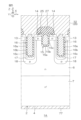
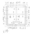
- FIG. 1 is a plan view showing the semiconductor device according to the first embodiment.
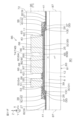
- FIG. FIG. 2 is a cross-sectional view taken along line II-II shown in FIG.
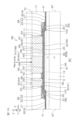
- FIG. 3 is a cross-sectional view taken along line III-III shown in FIG.
- FIG. 4 is an enlarged plan view showing the main part of the inner part of the chip.
- FIG. 5 is a cross-sectional view taken along line V-V shown in FIG.
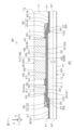
- FIG. 6 is an enlarged cross-sectional view showing the main part of the periphery of the chip.
- FIG. 7 is a plan view showing a layout example of gate electrodes and source electrodes.
- FIG. 8 is a plan view showing a layout example of the upper insulating film.
- FIG. 9 is a plan view showing the wafer structure used during fabrication.
- FIG. 10 is a cross-sectional view showing the device region shown in FIG. 9.
- FIG. 11A is a cross-sectional view showing an example of a method for manufacturing the semiconductor device shown in FIG. 1.
- FIG. 11B is a cross-sectional view showing a step after FIG. 11A.
- FIG. 11C is a cross-sectional view showing a step after FIG. 11B.
- FIG. 11D is a cross-sectional view showing a step after FIG. 11C.
- FIG. 11E is a cross-sectional view showing a step after FIG. 11D.
- FIG. 11F is a cross-sectional view showing a step after FIG. 11E.
- FIG. 11G is a cross-sectional view showing a step after FIG. 11F.
- FIG. 11A is a cross-sectional view showing an example of a method for manufacturing the semiconductor device shown in FIG. 1.
- FIG. 11B is a cross-sectional view showing a step after FIG. 11A.
- FIG. 11H is a cross-sectional view showing a step after FIG. 11G.
- FIG. 11I is a cross-sectional view showing a step after FIG. 11H.
- FIG. 12 is a plan view showing the semiconductor device according to the second embodiment.
- FIG. 13 is a plan view showing the semiconductor device according to the third embodiment.
- 14 is a cross-sectional view taken along line XIV-XIV shown in FIG. 13.
- FIG. 15 is a circuit diagram showing an electrical configuration of the semiconductor device shown in FIG. 13.
- FIG. FIG. 16 is a plan view showing the semiconductor device according to the fourth embodiment. 17 is a cross-sectional view taken along line XVII-XVII shown in FIG. 16.
- FIG. FIG. 18 is a plan view showing the semiconductor device according to the fifth embodiment.
- FIG. 19 is a plan view showing the semiconductor device according to the sixth embodiment.
- FIG. 20 is a plan view showing the semiconductor device according to the seventh embodiment.
- FIG. 21 is a plan view showing the semiconductor device according to the eighth embodiment.
- 22 is a cross-sectional view taken along line XXII-XXII shown in FIG. 21.
- FIG. 23 is a cross-sectional view showing a modification of the chip applied to each embodiment.
- FIG. 24 is a plan view showing a modification of the gap applied to each embodiment.
- FIG. 25 is a plan view showing a modification of the gap applied to each embodiment.
- FIG. 26 is a cross-sectional view showing a modification of the sealing insulator applied to each embodiment.
- FIG. 27 is a plan view showing a modification of the gate terminal electrode applied to each embodiment.
- FIG. 28 is a plan view showing a package in which the semiconductor devices according to the first to seventh embodiments are mounted.
- FIG. 29 is a plan view showing a package on which a semiconductor device according to the eighth embodiment is mounted;
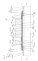
- FIG. 30 is a perspective view showing a package in which the semiconductor devices according to the first to seventh embodiments and the semiconductor device according to the eighth embodiment are mounted.
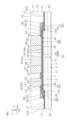
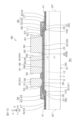
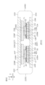
- 31 is an exploded perspective view of the package shown in FIG. 30;
- FIG. 32 is a cross-sectional view taken along line XXXII-XXXII shown in FIG. 30.
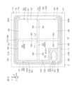
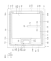
- FIG. 1 is a plan view showing a semiconductor device 1A according to the first embodiment.
- FIG. 2 is a cross-sectional view taken along line II-II shown in FIG.
- FIG. 3 is a cross-sectional view taken along line III-III shown in FIG.
- FIG. 4 is an enlarged plan view showing the main part of the inner part of the chip 2.
- FIG. 5 is a cross-sectional view taken along line V-V shown in FIG.
- FIG. 6 is an enlarged cross-sectional view showing the essential parts of the periphery of the chip 2.
- FIG. 7 is a plan view showing a layout example of the gate electrode 30 and the source electrode 32.
- FIG. FIG. 8 is a plan view showing a layout example of the upper insulating film 38. As shown in FIG.
- a semiconductor device 1A in this embodiment includes a chip 2 that includes a wide bandgap semiconductor single crystal and is formed in a hexahedral shape (specifically, a rectangular parallelepiped shape). include. That is, the semiconductor device 1A is a "wide bandgap semiconductor device". Chip 2 may also be referred to as a "semiconductor chip” or a "wide bandgap semiconductor chip”.
- a wide bandgap semiconductor is a semiconductor having a bandgap that exceeds the bandgap of Si (silicon). GaN (gallium nitride), SiC (silicon carbide) and C (diamond) are exemplified as wide bandgap semiconductors.
- the chip 2 is, in this embodiment, a "SiC chip" containing a hexagonal SiC single crystal as an example of a wide bandgap semiconductor. That is, the semiconductor device 1A is a "SiC semiconductor device". Hexagonal SiC single crystals have a plurality of polytypes including 2H (Hexagonal)-SiC single crystals, 4H-SiC single crystals, 6H-SiC single crystals and the like. In this form an example is shown in which the chip 2 comprises a 4H—SiC single crystal, but this does not exclude the choice of other polytypes.
- the chip 2 has a first main surface 3 on one side, a second main surface 4 on the other side, and first to fourth side surfaces 5A to 5D connecting the first main surface 3 and the second main surface 4. ing.
- the first main surface 3 and the second main surface 4 are formed in a quadrangular shape when viewed from the normal direction Z (hereinafter simply referred to as "plan view").
- the normal direction Z is also the thickness direction of the chip 2 .
- the first main surface 3 and the second main surface 4 are preferably formed by the c-plane of SiC single crystal.
- the first main surface 3 is formed by the silicon surface of the SiC single crystal
- the second main surface 4 is formed by the carbon surface of the SiC single crystal.
- the first main surface 3 and the second main surface 4 may have an off angle inclined at a predetermined angle in a predetermined off direction with respect to the c-plane.
- the off-direction is preferably the a-axis direction ([11-20] direction) of the SiC single crystal.
- the off angle may exceed 0° and be 10° or less.
- the off angle is preferably 5° or less.
- the second main surface 4 may be a ground surface having grinding marks, or may be a smooth surface having no grinding marks.
- the first side surface 5A and the second side surface 5B extend in the first direction X along the first main surface 3 and face the second direction Y intersecting (specifically, perpendicular to) the first direction X.
- the third side surface 5C and the fourth side surface 5D extend in the second direction Y and face the first direction X.
- the first direction X may be the m-axis direction ([1-100] direction) of the SiC single crystal
- the second direction Y may be the a-axis direction of the SiC single crystal.
- the first direction X may be the a-axis direction of the SiC single crystal
- the second direction Y may be the m-axis direction of the SiC single crystal.
- the first to fourth side surfaces 5A to 5D may be ground surfaces having grinding marks, or may be smooth surfaces having no grinding marks.
- the chip 2 may have a thickness of 5 ⁇ m or more and 250 ⁇ m or less with respect to the normal direction Z.
- the thickness of the chip 2 may be 100 ⁇ m or less.
- the thickness of the chip 2 is preferably 50 ⁇ m or less. It is particularly preferable that the thickness of the chip 2 is 40 ⁇ m or less.
- the first to fourth side surfaces 5A to 5D may have lengths of 0.5 mm or more and 10 mm or less in plan view.
- the length of the first to fourth side surfaces 5A to 5D is preferably 1 mm or more. It is particularly preferable that the lengths of the first to fourth side surfaces 5A to 5D are 2 mm or more. That is, it is preferable that the chip 2 has a plane area of 1 mm square or more (preferably 2 mm square or more) and a thickness of 100 ⁇ m or less (preferably 50 ⁇ m or less) in a cross-sectional view. The lengths of the first to fourth side surfaces 5A to 5D are set in the range of 4 mm or more and 6 mm or less in this embodiment.
- the semiconductor device 1A includes an n-type (first conductivity type) first semiconductor region 6 formed in a region (surface layer portion) on the first main surface 3 side within the chip 2 .
- the first semiconductor region 6 is formed in a layer extending along the first main surface 3 and exposed from the first main surface 3 and the first to fourth side surfaces 5A to 5D.
- the first semiconductor region 6 consists of an epitaxial layer (specifically, a SiC epitaxial layer) in this embodiment.
- the first semiconductor region 6 may have a thickness in the normal direction Z of 1 ⁇ m or more and 50 ⁇ m or less.
- the thickness of the first semiconductor region 6 is preferably 3 ⁇ m or more and 30 ⁇ m or less. It is particularly preferable that the thickness of the first semiconductor region 6 is 5 ⁇ m or more and 25 ⁇ m or less.
- the semiconductor device 1A includes an n-type second semiconductor region 7 formed in a region (surface layer portion) on the second main surface 4 side within the chip 2 .
- the second semiconductor region 7 is formed in a layer extending along the second main surface 4 and exposed from the second main surface 4 and the first to fourth side surfaces 5A to 5D.
- the second semiconductor region 7 has a higher n-type impurity concentration than the first semiconductor region 6 and is electrically connected to the first semiconductor region 6 .
- the second semiconductor region 7 is made of a semiconductor substrate (specifically, a SiC semiconductor substrate) in this embodiment. That is, the chip 2 has a laminated structure including a semiconductor substrate and an epitaxial layer.
- the second semiconductor region 7 may have a thickness of 1 ⁇ m or more and 200 ⁇ m or less with respect to the normal direction Z.
- the thickness of the second semiconductor region 7 is preferably 5 ⁇ m or more and 50 ⁇ m or less. It is particularly preferable that the thickness of the second semiconductor region 7 is 5 ⁇ m or more and 20 ⁇ m or less.
- the thickness of the second semiconductor region 7 is preferably 10 ⁇ m or more. Most preferably, the thickness of the second semiconductor region 7 is less than the thickness of the first semiconductor region 6 .
- the resistance value for example, on-resistance
- the thickness of the second semiconductor region 7 may exceed the thickness of the first semiconductor region 6 .
- the semiconductor device 1A includes an active surface 8 formed on the first main surface 3, an outer surface 9, and first to fourth connection surfaces 10A to 10D (connecting surfaces).
- the active surface 8, the outer surface 9 and the first to fourth connection surfaces 10A to 10D define a mesa portion 11 (plateau) on the first main surface 3.
- the active surface 8 may be called "first surface”
- the outer surface 9 may be called “second surface”
- the first to fourth connection surfaces 10A to 10D may be called “connection surfaces”.
- the active surface 8, the outer surface 9 and the first to fourth connection surfaces 10A-10D (that is, the mesa portion 11) may be regarded as components of the chip 2 (first main surface 3).
- the active surface 8 is formed spaced inwardly from the periphery of the first main surface 3 (first to fourth side surfaces 5A to 5D).
- the active surface 8 has a flat surface extending in the first direction X and the second direction Y. As shown in FIG. In this form, the active surface 8 is formed in a square shape having four sides parallel to the first to fourth side surfaces 5A to 5D in plan view.
- the outer surface 9 is located outside the active surface 8 and recessed from the active surface 8 in the thickness direction of the chip 2 (the second main surface 4 side). Specifically, the outer surface 9 is recessed to a depth less than the thickness of the first semiconductor region 6 so as to expose the first semiconductor region 6 .
- the outer side surface 9 extends in a belt shape along the active surface 8 in a plan view and is formed in an annular shape (specifically, a quadrangular annular shape) surrounding the active surface 8 .
- the outer side surface 9 has flat surfaces extending in the first direction X and the second direction Y and formed substantially parallel to the active surface 8 .
- the outer side surface 9 is continuous with the first to fourth side surfaces 5A to 5D.
- the first to fourth connection surfaces 10A to 10D extend in the normal direction Z and connect the active surface 8 and the outer surface 9.
- the first connection surface 10A is positioned on the first side surface 5A side
- the second connection surface 10B is positioned on the second side surface 5B side
- the third connection surface 10C is positioned on the third side surface 5C side
- the fourth connection surface 10D. is located on the side of the fourth side surface 5D.
- the first connection surface 10A and the second connection surface 10B extend in the first direction X and face the second direction Y.
- the third connection surface 10C and the fourth connection surface 10D extend in the second direction Y and face the first direction X.
- the first to fourth connection surfaces 10A to 10D may extend substantially vertically between the active surface 8 and the outer surface 9 so as to define a quadrangular prism-shaped mesa portion 11.
- the first to fourth connection surfaces 10A to 10D may be inclined downward from the active surface 8 toward the outer surface 9 so that the mesa portion 11 in the shape of a truncated square pyramid is defined.
- semiconductor device 1A includes mesa portion 11 formed in first semiconductor region 6 on first main surface 3 .
- the mesa portion 11 is formed only in the first semiconductor region 6 and not formed in the second semiconductor region 7 .
- a semiconductor device 1A includes a MISFET (Metal Insulator Semiconductor Field Effect Transistor) structure 12 formed on an active surface 8 (first main surface 3). 2 and 3, the MISFET structure 12 is shown simplified by dashed lines. A specific structure of the MISFET structure 12 will be described below with reference to FIGS. 4 and 5. FIG.
- MISFET Metal Insulator Semiconductor Field Effect Transistor
- the MISFET structure 12 includes a p-type (second conductivity type) body region 13 formed on the surface layer of the active surface 8 .
- the body region 13 is formed spaced from the bottom of the first semiconductor region 6 toward the active surface 8 side.
- Body region 13 is formed in a layered shape extending along active surface 8 .
- the body region 13 may be partially exposed from the first to fourth connection surfaces 10A to 10D.
- the MISFET structure 12 includes an n-type source region 14 formed on the surface layer of the body region 13 .
- the source region 14 has an n-type impurity concentration higher than that of the first semiconductor region 6 .
- the source region 14 is formed spaced from the bottom of the body region 13 toward the active surface 8 side.
- the source region 14 is formed in layers extending along the active surface 8 .
- Source region 14 may be exposed from the entire active surface 8 .
- the source region 14 may be exposed from part of the first to fourth connection surfaces 10A to 10D.
- Source region 14 forms a channel in body region 13 with first semiconductor region 6 .
- the MISFET structure 12 includes multiple gate structures 15 formed on the active surface 8 .
- the plurality of gate structures 15 are arranged in the first direction X at intervals in plan view, and are formed in strips extending in the second direction Y, respectively.
- a plurality of gate structures 15 extend through the body region 13 and the source region 14 to reach the first semiconductor region 6 .
- a plurality of gate structures 15 control channel inversion and non-inversion within the body region 13 .
- Each gate structure 15, in this form, includes a gate trench 15a, a gate insulating film 15b and a gate buried electrode 15c.
- a gate trench 15 a is formed in the active surface 8 and defines the walls of the gate structure 15 .
- the gate insulating film 15b covers the walls of the gate trench 15a.
- the gate buried electrode 15c is buried in the gate trench 15a with the gate insulating film 15b interposed therebetween and faces the channel with the gate insulating film 15b interposed therebetween.
- the MISFET structure 12 includes multiple source structures 16 formed on the active surface 8 .
- a plurality of source structures 16 are arranged in regions between a pair of adjacent gate structures 15 on the active surface 8 .
- the plurality of source structures 16 are each formed in a strip shape extending in the second direction Y in plan view.
- a plurality of source structures 16 extend through the body region 13 and the source region 14 to reach the first semiconductor region 6 .
- a plurality of source structures 16 have a depth that exceeds the depth of gate structures 15 .
- the plurality of source structures 16 specifically has a depth approximately equal to the depth of the outer surface 9 .
- Each source structure 16 includes a source trench 16a, a source insulating film 16b and a source buried electrode 16c.
- a source trench 16 a is formed in the active surface 8 and defines the walls of the source structure 16 .
- the source insulating film 16b covers the walls of the source trench 16a.
- the source buried electrode 16c is buried in the source trench 16a with the source insulating film 16b interposed therebetween.
- the MISFET structure 12 includes a plurality of p-type contact regions 17 respectively formed in regions along the plurality of source structures 16 within the chip 2 .
- a plurality of contact regions 17 have a higher p-type impurity concentration than body region 13 .
- Each contact region 17 covers the sidewalls and bottom walls of each source structure 16 and is electrically connected to body region 13 .
- the MISFET structure 12 includes a plurality of p-type well regions 18 respectively formed in regions along the plurality of source structures 16 within the chip 2 .
- Each well region 18 may have a p-type impurity concentration higher than body region 13 and lower than contact region 17 .
- Each well region 18 covers the corresponding source structure 16 with the corresponding contact region 17 interposed therebetween.
- Each well region 18 covers the sidewalls and bottom walls of corresponding source structure 16 and is electrically connected to body region 13 and contact region 17 .
- semiconductor device 1A includes p-type outer contact region 19 formed in the surface layer portion of outer side surface 9 .
- Outer contact region 19 has a p-type impurity concentration higher than that of body region 13 .
- the outer contact region 19 is formed in a band-like shape extending along the active surface 8 and spaced apart from the peripheral edge of the active surface 8 and the peripheral edge of the outer side surface 9 in plan view.
- the outer contact region 19 is formed in a ring shape (specifically, a square ring shape) surrounding the active surface 8 in plan view.
- the outer contact region 19 is formed spaced apart from the bottom of the first semiconductor region 6 to the outer side surface 9 .
- the outer contact region 19 is located on the bottom side of the first semiconductor region 6 with respect to the bottom walls of the plurality of gate structures 15 (source structures 16).
- the semiconductor device 1A includes a p-type outer well region 20 formed in the surface layer portion of the outer side surface 9 .
- the outer well region 20 has a p-type impurity concentration lower than that of the outer contact region 19 .
- the p-type impurity concentration of the outer well region 20 is preferably approximately equal to the p-type impurity concentration of the well region 18 .
- the outer well region 20 is formed in a region between the peripheral edge of the active surface 8 and the outer contact region 19 in plan view, and is formed in a strip shape extending along the active surface 8 .
- the outer well region 20 is formed in an annular shape (specifically, a quadrangular annular shape) surrounding the active surface 8 in plan view.
- the outer well region 20 is formed spaced apart from the bottom of the first semiconductor region 6 to the outer side surface 9 .
- the outer well region 20 may be formed deeper than the outer contact region 19 .
- the outer well region 20 is located on the bottom side of the first semiconductor region 6 with respect to the bottom walls of the plurality of gate structures 15 (source structures 16).
- the outer well region 20 is electrically connected to the outer contact region 19.
- the outer well region 20 extends from the outer contact region 19 side toward the first to fourth connection surfaces 10A to 10D and covers the first to fourth connection surfaces 10A to 10D.
- Outer well region 20 is electrically connected to body region 13 at the surface layer of active surface 8 .
- the semiconductor device 1A has at least one (preferably two or more and twenty or less) p-type field regions 21 formed in a region between the peripheral edge of the outer side surface 9 and the outer contact region 19 in the surface layer portion of the outer side surface 9. including.
- the semiconductor device 1A includes five field regions 21 in this form.
- a plurality of field regions 21 relax the electric field within the chip 2 at the outer surface 9 .
- the number, width, depth, p-type impurity concentration, etc. of the field regions 21 are arbitrary and can take various values according to the electric field to be relaxed.
- the plurality of field regions 21 are arranged at intervals from the outer contact region 19 side to the peripheral edge side of the outer surface 9 .
- the plurality of field regions 21 are formed in strips extending along the active surface 8 in plan view.
- the plurality of field regions 21 are formed in a ring shape (specifically, a square ring shape) surrounding the active surface 8 in plan view.
- the plurality of field regions 21 are each formed as an FLR (Field Limiting Ring) region.
- a plurality of field regions 21 are formed at intervals from the bottom of the first semiconductor region 6 to the outer surface 9 .
- the plurality of field regions 21 are located on the bottom side of the first semiconductor region 6 with respect to the bottom walls of the plurality of gate structures 15 (source structures 16).
- a plurality of field regions 21 may be formed deeper than the outer contact region 19 .
- the innermost field region 21 may be connected to the outer contact region 19 .
- the semiconductor device 1A includes a main surface insulating film 25 covering the first main surface 3.
- Main surface insulating film 25 may include at least one of a silicon oxide film, a silicon nitride film, and a silicon oxynitride film.
- the main surface insulating film 25 has a single layer structure made of a silicon oxide film in this embodiment.
- Main surface insulating film 25 particularly preferably includes a silicon oxide film made of oxide of chip 2 .
- the main surface insulating film 25 covers the active surface 8, the outer surface 9 and the first to fourth connection surfaces 10A to 10D.
- the main surface insulating film 25 continues to the gate insulating film 15b and the source insulating film 16b, and covers the active surface 8 so as to expose the gate buried electrode 15c and the source buried electrode 16c.
- the main surface insulating film 25 covers the outer surface 9 and the first to fourth connection surfaces 10A to 10D so as to cover the outer contact region 19, the outer well region 20 and the plurality of field regions 21. As shown in FIG.
- the main surface insulating film 25 may be continuous with the first to fourth side surfaces 5A to 5D.
- the outer wall of the main surface insulating film 25 may be a ground surface having grinding marks.
- the outer wall of the main surface insulating film 25 may form one ground surface together with the first to fourth side surfaces 5A to 5D.
- the outer wall of the main surface insulating film 25 may be formed with a space inwardly from the peripheral edge of the outer surface 9 to expose the first semiconductor region 6 from the peripheral edge of the outer surface 9 .
- the semiconductor device 1A includes a sidewall structure 26 formed on the main surface insulating film 25 so as to cover at least one of the first to fourth connection surfaces 10A to 10D on the outer surface 9.
- the sidewall structure 26 is formed in an annular shape (square annular shape) surrounding the active surface 8 in plan view.
- the sidewall structure 26 may have a portion overlying the active surface 8 .
- Sidewall structure 26 may comprise an inorganic insulator or polysilicon.
- Sidewall structure 26 may be a sidewall interconnect electrically connected to source structure 16 .
- the semiconductor device 1A includes an interlayer insulating film 27 formed on the main surface insulating film 25 .
- Interlayer insulating film 27 may include at least one of a silicon oxide film, a silicon nitride film, and a silicon oxynitride film.
- the interlayer insulating film 27 has a single-layer structure made of a silicon oxide film in this embodiment.
- the interlayer insulating film 27 covers the active surface 8, the outer side surface 9 and the first to fourth connection surfaces 10A to 10D with the main surface insulating film 25 interposed therebetween. Specifically, the interlayer insulating film 27 covers the active surface 8, the outer side surface 9 and the first to fourth connection surfaces 10A to 10D with the sidewall structure 26 interposed therebetween. The interlayer insulating film 27 covers the MISFET structure 12 on the active surface 8 side, and covers the outer contact region 19, the outer well region 20 and the plurality of field regions 21 on the outer side surface 9 side.
- the interlayer insulating film 27 continues to the first to fourth side surfaces 5A to 5D in this form.
- the outer wall of the interlayer insulating film 27 may be a ground surface having grinding marks.
- the outer wall of the interlayer insulating film 27 may form one ground surface together with the first to fourth side surfaces 5A to 5D.
- the outer wall of the interlayer insulating film 27 may be formed spaced inwardly from the peripheral edge of the outer side surface 9 to expose the first semiconductor region 6 from the peripheral edge portion of the outer side surface 9 .
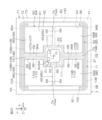
- the semiconductor device 1A includes a gate electrode 30 arranged on the first main surface 3 (interlayer insulating film 27).
- Gate electrode 30 may be referred to as a “gate main surface electrode”.
- the gate electrode 30 is arranged in the inner part of the first main surface 3 with a space from the peripheral edge of the first main surface 3 .
- a gate electrode 30 is arranged above the active surface 8 in this embodiment.
- the gate electrode 30 is arranged in a region on the periphery of the active surface 8 and close to the central portion of the third connection surface 10C (third side surface 5C).
- the gate electrode 30 is formed in a square shape in plan view.
- the gate electrode 30 may be formed in a polygonal shape other than a square shape, a circular shape, or an elliptical shape in plan view.
- the gate electrode 30 preferably has a plane area of 25% or less of the first main surface 3.
- the planar area of gate electrode 30 may be 10% or less of first main surface 3 .
- the gate electrode 30 may have a thickness of 0.5 ⁇ m or more and 15 ⁇ m or less.
- Gate electrode 30 includes a gate lower conductor layer 31 .
- the gate lower conductor layer 31 may include at least one of a Ti film, a TiN film, a W film, an Al film, a Cu film, an Al alloy film, a Cu alloy film and a conductive polysilicon film.
- the gate lower conductor layer 31 includes a pure Cu film (a Cu film with a purity of 99% or more), a pure Al film (an Al film with a purity of 99% or more), an AlCu alloy film, an AlSi alloy film, and an AlSiCu alloy film. may include at least one of In this embodiment, the gate lower conductor layer 31 has a laminated structure including a Ti film and an Al alloy film (AlSiCu alloy film in this embodiment) laminated in this order from the chip 2 side.
- the semiconductor device 1A includes a source electrode 32 spaced from the gate electrode 30 and arranged on the first main surface 3 (interlayer insulating film 27).
- the source electrode 32 may be referred to as a "source main surface electrode”.
- the source electrode 32 is arranged in the inner part of the first main surface 3 with a space from the periphery of the first main surface 3 .
- a source electrode 32 is arranged on the active surface 8 in this embodiment.
- the source electrode 32 has a body electrode portion 33 and at least one (in this embodiment, a plurality of) extraction electrode portions 34A and 34B.
- the body electrode portion 33 is arranged in a region on the side of the fourth side surface 5D (fourth connection surface 10D) with a gap from the gate electrode 30 in plan view, and faces the gate electrode 30 in the first direction X.
- the body electrode portion 33 is formed in a polygonal shape (specifically, a rectangular shape) having four sides parallel to the first to fourth side surfaces 5A to 5D in plan view.
- the multiple lead electrode portions 34A and 34B include a first lead electrode portion 34A on one side (first side surface 5A side) and a second lead electrode portion 34B on the other side (second side surface 5B side).
- the first extraction electrode portion 34A is extracted from the body electrode portion 33 to a region located on one side (first side surface 5A side) in the second direction Y with respect to the gate electrode 30 in plan view, and extends in the second direction Y to the gate electrode portion 34A. It faces the electrode 30 .
- the second extraction electrode portion 34B is extracted from the body electrode portion 33 to a region located on the other side (the second side surface 5B side) in the second direction Y with respect to the gate electrode 30 in plan view, and extends in the second direction Y to the gate electrode portion 34B. It faces the electrode 30 . That is, the plurality of extraction electrode portions 34A and 34B sandwich the gate electrode 30 from both sides in the second direction Y in plan view.
- the source electrode 32 (body electrode portion 33 and lead-out electrode portions 34A and 34B) penetrates the interlayer insulating film 27 and the main surface insulating film 25 and electrically connects the plurality of source structures 16, the source regions 14 and the plurality of well regions 18. It is connected to the.
- the source electrode 32 may be composed of only the body electrode portion 33 without the lead electrode portions 34A and 34B.
- the source electrode 32 has a planar area that exceeds the planar area of the gate electrode 30 .
- the plane area of the source electrode 32 is preferably 50% or more of the first main surface 3 . It is particularly preferable that the plane area of the source electrode 32 is 75% or more of the first main surface 3 .
- the source electrode 32 includes a source lower conductor layer 35 .
- the source lower conductor layer 35 may include at least one of a Ti film, a TiN film, a W film, an Al film, a Cu film, an Al alloy film, a Cu alloy film and a conductive polysilicon film.
- the source lower conductor layer 35 includes a pure Cu film (a Cu film with a purity of 99% or higher), a pure Al film (an Al film with a purity of 99% or higher), an AlCu alloy film, an AlSi alloy film, and an AlSiCu alloy film. preferably includes at least one of
- the source lower conductor layer 35 has a laminated structure including a Ti film and an Al alloy film (AlSiCu alloy film in this embodiment) laminated in this order from the chip 2 side.
- Source lower conductor layer 35 preferably comprises the same conductive material as gate lower conductor layer 31 .
- the source lower conductor layer 35 (source electrode 32) may have a thickness of 0.5 ⁇ m or more and 15 ⁇ m or less.
- the semiconductor device 1A includes at least one (a plurality in this embodiment) gate wirings 36A and 36B drawn from the gate electrode 30 onto the first main surface 3 (interlayer insulating film 27).
- the plurality of gate wirings 36A, 36B includes the gate lower conductor layer 31, similar to the gate electrode 30. As shown in FIG. A plurality of gate lines 36A, 36B cover the active surface 8 and do not cover the outer surface 9 in this configuration.
- a plurality of gate wirings 36A and 36B are led out to a region between the peripheral edge of the active surface 8 and the source electrode 32 in a plan view, and extend along the source electrode 32 in a strip shape.
- the plurality of gate wirings 36A, 36B specifically includes a first gate wiring 36A and a second gate wiring 36B.
- the first gate wiring 36A is drawn from the gate electrode 30 to a region on the first side surface 5A side in plan view.
- the first gate line 36A has a strip-like portion extending in the second direction Y along the third side surface 5C and a strip-like portion extending in the first direction X along the first side surface 5A.
- the second gate wiring 36B is drawn from the gate electrode 30 to a region on the second side surface 5B side in plan view.
- the second gate line 36B has a strip-like portion extending in the second direction Y along the third side surface 5C and a strip-like portion extending in the first direction X along the second side surface 5B.
- the plurality of gate wirings 36A and 36B intersect (specifically, perpendicularly) both ends of the plurality of gate structures 15 at the periphery of the active surface 8 (first main surface 3).
- the multiple gate wirings 36A and 36B are electrically connected to the multiple gate structures 15 through the interlayer insulating film 27 .
- the plurality of gate wirings 36A and 36B may be directly connected to the plurality of gate structures 15, or may be electrically connected to the plurality of gate structures 15 via a conductor film.
- the semiconductor device 1A includes a source wiring 37 drawn from the source electrode 32 onto the first main surface 3 (interlayer insulating film 27).
- the source line 37 includes a source lower conductor layer 35 as does the source electrode 32 .
- the source wiring 37 is formed in a strip shape extending along the periphery of the active surface 8 in a region closer to the outer surface 9 than the plurality of gate wirings 36A and 36B.
- the source wiring 37 is formed in a ring shape (specifically, a square ring shape) surrounding the gate electrode 30, the source electrode 32 and the plurality of gate wirings 36A and 36B in plan view.
- the source wiring 37 covers the sidewall structure 26 with the interlayer insulating film 27 interposed therebetween, and is drawn out from the active surface 8 side to the outer surface 9 side.
- the source wiring 37 preferably covers the entire sidewall structure 26 over the entire circumference.
- Source line 37 has a portion that penetrates interlayer insulating film 27 and main surface insulating film 25 on the side of outer surface 9 and is connected to outer surface 9 (specifically, outer contact region 19).
- the source wiring 37 may be electrically connected to the sidewall structure 26 through the interlayer insulating film 27 .
- the semiconductor device 1A includes an upper insulating film 38 that selectively covers the gate electrode 30, the source electrode 32, the plurality of gate wirings 36A and 36B, and the source wiring 37.
- the upper insulating film 38 has a gate opening 39 that exposes the inner portion of the gate electrode 30 and covers the peripheral portion of the gate electrode 30 over the entire circumference.
- the gate opening 39 is formed in a square shape in plan view.
- the upper insulating film 38 has a source opening 40 that exposes the inner part of the source electrode 32 in plan view, and covers the peripheral edge of the source electrode 32 over the entire circumference.
- the source opening 40 is formed in a polygonal shape along the source electrode 32 in plan view.
- the upper insulating film 38 covers the entire area of the plurality of gate wirings 36A and 36B and the entire area of the source wiring 37 .
- the upper insulating film 38 covers the sidewall structure 26 with the interlayer insulating film 27 interposed therebetween, and extends from the active surface 8 side to the outer surface 9 side.
- the upper insulating film 38 is formed spaced inwardly from the periphery of the outer side surface 9 (first to fourth side surfaces 5A to 5D) and covers the outer contact region 19, the outer well region 20 and the plurality of field regions 21. are doing.
- the upper insulating film 38 partitions the dicing streets 41 with the periphery of the outer side surface 9 .
- the dicing street 41 is formed in a strip shape extending along the peripheral edges (first to fourth side surfaces 5A to 5D) of the outer side surface 9 in plan view.
- the dicing street 41 is formed in an annular shape (specifically, a quadrangular annular shape) surrounding the inner portion (active surface 8) of the first main surface 3 in plan view.
- the dicing street 41 exposes the interlayer insulating film 27 in this form.
- the dicing streets 41 may expose the outer surface 9 .
- the dicing street 41 may have a width of 1 ⁇ m or more and 200 ⁇ m or less.
- the width of the dicing street 41 is the width in the direction perpendicular to the extending direction of the dicing street 41 .
- the width of the dicing street 41 is preferably 5 ⁇ m or more and 50 ⁇ m or less.
- the upper insulating film 38 preferably has a thickness exceeding the thickness of the gate electrode 30 and the thickness of the source electrode 32 .
- the thickness of the upper insulating film 38 is preferably less than the thickness of the chip 2 .
- the thickness of the upper insulating film 38 may be 3 ⁇ m or more and 35 ⁇ m or less.
- the thickness of the upper insulating film 38 is preferably 25 ⁇ m or less.
- the upper insulating film 38 has a laminated structure including an inorganic insulating film 42 and an organic insulating film 43 laminated in this order from the chip 2 side.
- the upper insulating film 38 may include at least one of the inorganic insulating film 42 and the organic insulating film 43, and does not necessarily include the inorganic insulating film 42 and the organic insulating film 43 at the same time.
- the inorganic insulating film 42 selectively covers the gate electrode 30, the source electrode 32, the plurality of gate wirings 36A and 36B, and the source wiring 37, and partially covers the gate opening 39, the source opening 40, and the dicing street 41. Some are partitioned.
- the inorganic insulating film 42 may include at least one of a silicon oxide film, a silicon nitride film and a silicon oxynitride film.
- the inorganic insulating film 42 preferably contains an insulating material different from that of the interlayer insulating film 27 .
- the inorganic insulating film 42 preferably contains a silicon nitride film.
- the inorganic insulating film 42 preferably has a thickness less than the thickness of the interlayer insulating film 27 .
- the inorganic insulating film 42 may have a thickness of 0.1 ⁇ m or more and 5 ⁇ m or less.
- the organic insulating film 43 selectively covers the inorganic insulating film 42 and partitions part of the gate opening 39 , part of the source opening 40 and part of the dicing street 41 . Specifically, the organic insulating film 43 partially exposes the inorganic insulating film 42 on the wall surface of the gate opening 39 . Also, the organic insulating film 43 partially exposes the inorganic insulating film 42 on the wall surface of the source opening 40 . Further, the organic insulating film 43 partially exposes the inorganic insulating film 42 on the wall surface of the dicing street 41 .
- the organic insulating film 43 may cover the inorganic insulating film 42 so that the inorganic insulating film 42 is not exposed from the wall surface of the gate opening 39 .
- the organic insulating film 43 may cover the inorganic insulating film 42 so that the inorganic insulating film 42 is not exposed from the wall surface of the source opening 40 .
- the organic insulating film 43 may cover the inorganic insulating film 42 so that the inorganic insulating film 42 is not exposed from the wall surfaces of the dicing streets 41 . In these cases, the organic insulating film 43 may cover the entire inorganic insulating film 42 .
- the organic insulating film 43 is preferably made of a resin film other than thermosetting resin.
- the organic insulating film 43 may be made of translucent resin or transparent resin.
- the organic insulating film 43 may be made of a negative type or positive type photosensitive resin film.
- the organic insulating film 43 is preferably made of a polyimide film, a polyamide film, or a polybenzoxazole film.
- the organic insulating film 43 includes a polybenzoxazole film in this form.
- the organic insulating film 43 preferably has a thickness exceeding the thickness of the inorganic insulating film 42 .
- the thickness of the organic insulating film 43 preferably exceeds the thickness of the interlayer insulating film 27 . It is particularly preferable that the thickness of the organic insulating film 43 exceeds the thickness of the gate electrode 30 and the thickness of the source electrode 32 .
- the thickness of the organic insulating film 43 may be 3 ⁇ m or more and 30 ⁇ m or less.
- the thickness of the organic insulating film 43 is preferably 20 ⁇ m or less.
- the semiconductor device 1A includes a gate terminal electrode 50 arranged on the gate electrode 30 .
- the gate terminal electrode 50 is erected in a pillar shape on a portion of the gate electrode 30 exposed from the gate opening 39 .
- the gate terminal electrode 50 has an area smaller than that of the gate electrode 30 in a plan view, and is arranged above the inner portion of the gate electrode 30 with a gap from the periphery of the gate electrode 30 .
- the gate terminal electrode 50 has a gate terminal surface 51 and gate terminal sidewalls 52 .
- Gate terminal surface 51 extends flat along first main surface 3 .
- the gate terminal surface 51 may be a ground surface having grinding marks.
- the gate terminal side wall 52 is located on the upper insulating film 38 (more specifically, the organic insulating film 43) in this embodiment.
- the gate terminal electrode 50 includes portions in contact with the inorganic insulating film 42 and the organic insulating film 43 .
- the gate terminal sidewall 52 extends substantially vertically in the normal direction Z. As shown in FIG. "Substantially vertical” also includes a form extending in the stacking direction while curving (meandering).
- Gate terminal sidewall 52 includes a portion facing gate electrode 30 with upper insulating film 38 interposed therebetween.
- the gate terminal side walls 52 are preferably smooth surfaces without grinding marks.
- the gate terminal electrode 50 has a first projecting portion 53 projecting outward from the lower end portion of the gate terminal side wall 52 .
- the first projecting portion 53 is formed in a region closer to the upper insulating film 38 (organic insulating film 43 ) than the intermediate portion of the gate terminal side wall 52 .
- the first projecting portion 53 extends along the outer surface of the upper insulating film 38 in a cross-sectional view, and is formed in a tapered shape in which the thickness gradually decreases from the gate terminal side wall 52 toward the tip portion.
- the first projecting portion 53 has a sharp tip that forms an acute angle.
- the gate terminal electrode 50 without the first projecting portion 53 may be formed.
- the gate terminal electrode 50 preferably has a thickness exceeding the thickness of the gate electrode 30 .
- the thickness of gate terminal electrode 50 is defined by the distance between gate electrode 30 and gate terminal surface 51 . It is particularly preferable that the thickness of the gate terminal electrode 50 exceeds the thickness of the upper insulating film 38 .
- the thickness of the gate terminal electrode 50 exceeds the thickness of the chip 2 in this embodiment. Of course, the thickness of the gate terminal electrode 50 may be less than the thickness of the chip 2 .
- the thickness of the gate terminal electrode 50 may be 10 ⁇ m or more and 300 ⁇ m or less.
- the thickness of the gate terminal electrode 50 is preferably 30 ⁇ m or more. It is particularly preferable that the thickness of the gate terminal electrode 50 is 80 ⁇ m or more and 200 ⁇ m or less.
- the planar area of the gate terminal electrode 50 is adjusted according to the planar area of the first main surface 3 .
- the planar area of the gate terminal electrode 50 is defined by the planar area of the gate terminal surface 51 .
- the planar area of gate terminal electrode 50 is preferably 25% or less of first main surface 3 .
- the planar area of the gate terminal electrode 50 may be 10% or less of the first main surface 3 .
- the plane area of the gate terminal electrode 50 may be 0.4 mm square or more.
- Gate terminal electrode 50 may be formed in a polygonal shape (for example, rectangular shape) having a plane area of 0.4 mm ⁇ 0.7 mm or more.
- the gate terminal electrode 50 is formed in a polygonal shape (quadrangular shape with four rectangular notched corners) having four sides parallel to the first to fourth side surfaces 5A to 5D in plan view.
- the gate terminal electrode 50 may be formed in a rectangular shape, a polygonal shape other than a rectangular shape, a circular shape, or an elliptical shape in plan view.
- the gate terminal electrode 50 includes a gate conductor layer 54 covering the gate electrode 30 .
- the gate conductor layer 54 covers the gate electrode 30 and the upper insulating film 38 within the gate opening 39 in this embodiment.
- the gate conductor layer 54 uniformly covers the gate electrode 30 and the upper insulating film 38 . Therefore, the gate terminal electrode 50 does not include a gap penetrating through the gate conductor layer 54 in the thickness direction.
- the gate conductor layer 54 has a laminated structure including a first gate conductor film 55 and a second gate conductor film 56 laminated in this order from the gate electrode 30 side.
- the first gate conductor film 55 may contain a Ti-based metal film.
- the first gate conductor film 55 may have a single layer structure made of a Ti film or a TiN film.
- the first gate conductor film 55 may have a laminated structure including a Ti film and a TiN film laminated in any order.
- the first gate conductor film 55 has a thickness less than the thickness of the gate electrode 30 .
- the first gate conductor film 55 covers the gate electrode 30 in the form of a film in the gate opening 39 and is pulled out on the upper insulating film 38 in the form of a film.
- the first gate conductor film 55 forms part of the first projecting portion 53 .
- the first gate conductor film 55 is not necessarily formed and may be removed.
- the second gate conductor film 56 forms the main body of the gate terminal electrode 50 .
- the second gate conductor film 56 may contain a Cu-based metal film.
- the Cu-based metal film may be a pure Cu film (a Cu film with a purity of 99% or more) or a Cu alloy film.
- the second gate conductor film 56 includes a pure Cu plating film in this embodiment.
- the second gate conductor film 56 preferably has a thickness exceeding the thickness of the gate electrode 30 . It is particularly preferable that the thickness of the second gate conductor film 56 exceeds the thickness of the upper insulating film 38 . The thickness of the second gate conductor film 56 exceeds the thickness of the chip 2 in this embodiment.
- the second gate conductor film 56 covers the gate electrode 30 in the gate opening 39 with the first gate conductor film 55 interposed therebetween, and is pulled out in the form of a film onto the upper insulating film 38 with the first gate conductor film 55 interposed therebetween. ing.
- the second gate conductor film 56 forms part of the first projecting portion 53 . That is, the first projecting portion 53 has a laminated structure including the first gate conductor film 55 and the second gate conductor film 56 .
- the second gate conductor film 56 preferably has a thickness exceeding the thickness of the first gate conductor film 55 within the first projecting portion 53 .
- the semiconductor device 1A includes a source terminal electrode 60 arranged on the source electrode 32 .
- the source terminal electrode 60 is erected in a columnar shape on a portion of the source electrode 32 exposed from the source opening 40 .
- the source terminal electrode 60 may have an area smaller than the area of the source electrode 32 in a plan view, and may be arranged above the inner portion of the source electrode 32 with a gap from the periphery of the source electrode 32 .
- the source terminal electrode 60 is formed in a polygonal shape (quadrangular in this form) having four sides parallel to the first to fourth side surfaces 5A to 5D in plan view.
- the source terminal electrode 60 has a source terminal surface 61 and source terminal sidewalls 62 .
- the source terminal surface 61 extends flat along the first main surface 3 .
- the source terminal surface 61 may be a ground surface having grinding marks.
- the source terminal sidewall 62 is located on the upper insulating film 38 (specifically, the organic insulating film 43) in this embodiment.
- the source terminal electrode 60 includes portions in contact with the inorganic insulating film 42 and the organic insulating film 43 .
- the source terminal sidewall 62 extends substantially vertically in the normal direction Z. As shown in FIG. "Substantially vertical” also includes a form extending in the stacking direction while curving (meandering).
- Source terminal sidewall 62 includes a portion facing source electrode 32 with upper insulating film 38 interposed therebetween.
- the source terminal sidewall 62 preferably has a smooth surface without grinding marks.
- the source terminal electrode 60 has a second projecting portion 63 projecting outward from the lower end portion of the source terminal side wall 62 in this embodiment.
- the second projecting portion 63 is formed in a region closer to the upper insulating film 38 (organic insulating film 43 ) than the intermediate portion of the source terminal side wall 62 .
- the second projecting portion 63 extends along the outer surface of the upper insulating film 38 in a cross-sectional view, and is formed in a tapered shape in which the thickness gradually decreases from the source terminal side wall 62 toward the tip portion.
- the second projecting portion 63 has a sharp tip that forms an acute angle.
- the source terminal electrode 60 without the second projecting portion 63 may be formed.
- the source terminal electrode 60 preferably has a thickness exceeding the thickness of the source electrode 32 .
- the thickness of source terminal electrode 60 is defined by the distance between source electrode 32 and source terminal surface 61 . It is particularly preferable that the thickness of the source terminal electrode 60 exceeds the thickness of the upper insulating film 38 . The thickness of the source terminal electrode 60 exceeds the thickness of the chip 2 in this embodiment.
- the thickness of the source terminal electrode 60 may be less than the thickness of the chip 2.
- the thickness of the source terminal electrode 60 may be 10 ⁇ m or more and 300 ⁇ m or less.
- the thickness of the source terminal electrode 60 is preferably 30 ⁇ m or more. It is particularly preferable that the thickness of the source terminal electrode 60 is 80 ⁇ m or more and 200 ⁇ m or less.
- the thickness of the source terminal electrode 60 is approximately equal to the thickness of the gate terminal electrode 50 .
- the source terminal electrode 60 includes a source conductor layer 64 , at least one (plurality in this embodiment) source gap portion 65 and at least one (plurality in this embodiment) source terminal portion 66 .
- the source conductor layer 64 covers the source electrode 32 and the upper insulating film 38 within the source opening 40 in this embodiment.
- the source conductor layer 64 has a laminated structure including a first source conductor film 67 and a second source conductor film 68 laminated in this order from the source electrode 32 side.
- the first source conductor film 67 may contain a Ti-based metal film.
- the first source conductor film 67 may have a single layer structure made of a Ti film or a TiN film.
- the first source conductor film 67 may have a laminated structure including a Ti film and a TiN film laminated in any order.
- the first source conductor film 67 is preferably made of the same conductive material as the first gate conductor film 55 .
- the first source conductor film 67 has a thickness less than the thickness of the source electrode 32 .
- the first source conductor film 67 covers the source electrode 32 in the form of a film in the source opening 40 and is pulled out on the upper insulating film 38 in the form of a film.
- the first source conductor film 67 forms part of the second projecting portion 63 .
- the thickness of the first source conductor film 67 is approximately equal to the thickness of the first gate conductor film 55 .
- the first source conductor film 67 does not necessarily have to be formed and may be removed.
- the second source conductor film 68 forms the main body of the source terminal electrode 60 .
- the second source conductor film 68 may contain a Cu-based metal film.
- the Cu-based metal film may be a pure Cu film (a Cu film with a purity of 99% or more) or a Cu alloy film.
- the second source conductor film 68 includes a pure Cu plating film in this embodiment.
- the second source conductor film 68 is preferably made of the same conductive material as the second gate conductor film 56 .
- the second source conductor film 68 preferably has a thickness exceeding the thickness of the source electrode 32 . It is particularly preferable that the thickness of the second source conductor film 68 exceeds the thickness of the upper insulating film 38 . The thickness of the second source conductor film 68 exceeds the thickness of the chip 2 in this form. The thickness of the second source conductor film 68 is approximately equal to the thickness of the second gate conductor film 56 .
- the second source conductor film 68 covers the source electrode 32 in the source opening 40 with the first source conductor film 67 interposed therebetween, and is pulled out in the form of a film onto the upper insulating film 38 with the first source conductor film 67 interposed therebetween. ing.
- the second source conductor film 68 forms part of the second projecting portion 63 . That is, the second projecting portion 63 has a laminated structure including the first source conductor film 67 and the second source conductor film 68 .
- the second source conductor film 68 preferably has a thickness exceeding the thickness of the first source conductor film 67 within the second protruding portion 63 .
- the source gap portion 65 penetrates the source conductor layer 64 in a cross-sectional view, and partitions the source conductor layer 64 into a plurality of portions (regions).
- the source gap 65 is formed at a position overlapping with the source electrode 32 to expose a portion of the source electrode 32 .
- the source gap 65 also exposes a portion of the upper insulating film 38 in this form.
- Source gap 65 in this form, includes a first source gap 65A and a second source gap 65B extending in different directions.
- the first source gap portion 65A is formed in a strip shape extending in the first direction X in plan view, and divides the source conductor layer 64 in the second direction Y. In this form, the first source gap portion 65A crosses the central portion of the source conductor layer 64 in the first direction X in plan view.
- the second source gap portion 65B is formed in a strip shape extending in the second direction Y so as to cross the first source gap portion 65A in plan view, and divides the source conductor layer 64 in the first direction X. As shown in FIG.
- the second source gap portion 65B crosses the central portion of the source conductor layer 64 in the second direction Y in plan view. That is, the second source gap 65B intersects the first source gap 65A at the central portion of the source conductor layer 64. As shown in FIG. The intersecting portion of the first source gap portion 65A and the second source gap portion 65B faces the gate terminal electrode 50 in the first direction X in plan view.
- the first source gap portion 65A may cross the central portion of the first main surface 3 (chip 2) in the first direction X in plan view.
- the second source gap portion 65B may cross the central portion of the first main surface 3 (chip 2) in the second direction Y in plan view.
- the first source gap portion 65A may be formed so as to be shifted in the second direction Y from the central portion of the source conductor layer 64 .
- the second source gap portion 65B may be formed so as to be shifted in the first direction X from the central portion of the source conductor layer 64 .
- the source gap portion 65 does not necessarily include both the first source gap portion 65A and the second source gap portion 65B at the same time, and includes only one of the first source gap portion 65A and the second source gap portion 65B. You can
- the multiple source terminal portions 66 are composed of multiple portions partitioned by the source gap portions 65 in the source conductor layer 64 . That is, in this form, four source terminal portions 66 are partitioned by the first source gap portion 65A and the second source gap portion 65B.
- the plurality of source terminal portions 66 are each fixed at the same potential as the source electrode 32 . That is, the source terminal electrode 60 is configured such that a source potential (single potential) is applied to one source electrode 32 via a plurality of source terminal portions 66 .
- the plurality of source terminal portions 66 are arranged on the body electrode portion 33 of the source electrode 32 and are not arranged on the extraction electrode portions 34A and 34B of the source electrode 32. Thereby, the facing area between the gate terminal electrode 50 and the source terminal portion 66 is reduced.
- Such a structure reduces the risk of shorting between the gate terminal electrode 50 and the source terminal portion 66 when a conductive adhesive such as solder or metal paste is attached to the gate terminal electrode 50 and the source terminal portion 66. is valid.
- a conductive joining member such as a conductive plate or a conductive wire (eg, bonding wire) may be connected to the gate terminal electrode 50 and the source terminal portion 66 . In this case, the risk of short-circuiting between the conductive joint member on the gate terminal electrode 50 side and the conductive joint member on the source terminal portion 66 side can be reduced.
- the plurality of source terminal portions 66 each have source gap sidewalls 69 partitioned by the source gap portions 65 .
- the source gap sidewall 69 preferably has a smooth surface without grinding marks.
- the plurality of source terminal portions 66 each have a second projecting portion 63 at the lower end portion of the source gap side wall 69 in this embodiment. The second projecting portion 63 on the side of the source gap sidewall 69 is positioned above the source electrode 32 .
- each source terminal portion 66 is adjusted according to the plane area of the first main surface 3 .
- the plane area of each source terminal portion 66 is defined by the plane area of the portion of source terminal surface 61 defined by source terminal sidewall 62 and source gap sidewall 69 .
- the total planar area of the plurality of source terminal portions 66 preferably exceeds the planar area of the gate terminal electrode 50 .
- the plane area of each source terminal portion 66 is preferably equal to or greater than the plane area of the gate terminal electrode 50 . It is particularly preferable that the plane area of each source terminal portion 66 exceeds the plane area of the gate terminal electrode 50 .
- the total plane area of the plurality of source terminal portions 66 is preferably 50% or more of the first main surface 3 . It is particularly preferable that the total plane area of the plurality of source terminal portions 66 is 75% or more of the first main surface 3 .
- each source terminal portion 66 is preferably 0.8 mm square or more. In this case, it is particularly preferable that the plane area of each source terminal portion 66 is 1 mm square or more.
- Each source terminal portion 66 may be formed in a polygonal shape having a plane area of 1 mm ⁇ 1.4 mm or more.
- Each source terminal portion 66 is formed in a square shape having four sides parallel to the first to fourth side surfaces 5A to 5D in plan view.
- each source terminal portion 66 may be formed in a polygonal shape other than a square shape, a circular shape, or an elliptical shape in plan view.
- the semiconductor device 1A includes a sealing insulator 71 that covers the first main surface 3.
- the sealing insulator 71 covers the periphery of the gate terminal electrode 50 and the periphery of the source terminal electrode 60 so as to expose a portion of the gate terminal electrode 50 and a portion of the source terminal electrode 60 on the first main surface 3 . are doing.
- the encapsulating insulator 71 covers the active surface 8, the outer surface 9 and the first to fourth connection surfaces 10A to 10D so as to expose the gate terminal electrode 50 and the source terminal electrode 60. As shown in FIG.
- the encapsulation insulator 71 exposes the gate terminal surface 51 and the source terminal surface 61 and covers the gate terminal sidewalls 52 and the source terminal sidewalls 62 .
- the sealing insulator 71 covers the first projecting portion 53 of the gate terminal electrode 50 and faces the upper insulating film 38 with the first projecting portion 53 interposed therebetween.
- the sealing insulator 71 prevents the gate terminal electrode 50 from coming off.
- the sealing insulator 71 covers the second projecting portion 63 of the source terminal electrode 60 and faces the upper insulating film 38 with the second projecting portion 63 interposed therebetween.
- the sealing insulator 71 prevents the source terminal electrode 60 from coming off.
- the sealing insulator 71 covers the dicing street 41 at the periphery of the outer surface 9 .
- the sealing insulator 71 directly covers the interlayer insulating film 27 at the dicing street 41 in this embodiment.
- the sealing insulator 71 directly covers the chip 2 and the main surface insulating film 25 on the dicing street 41.
- the sealing insulator 71 has an insulating main surface 72 and insulating side walls 73 .
- the insulating main surface 72 extends flat along the first main surface 3 .
- Insulating main surface 72 forms one flat surface with gate terminal surface 51 and source terminal surface 61 .
- the insulating main surface 72 may be a ground surface having grinding marks. In this case, the insulating main surface 72 preferably forms one ground surface together with the gate terminal surface 51 and the source terminal surface 61 .
- the insulating side wall 73 extends from the periphery of the insulating main surface 72 toward the chip 2 and forms one flat surface together with the first to fourth side surfaces 5A to 5D.
- the insulating side wall 73 is formed substantially perpendicular to the insulating main surface 72 .
- the angle formed between insulating side wall 73 and insulating main surface 72 may be 88° or more and 92° or less.
- the insulating side wall 73 may consist of a ground surface with grinding marks.
- the insulating sidewall 73 may form one grinding surface with the first to fourth side surfaces 5A to 5D.
- the encapsulating insulator 71 preferably has a thickness exceeding the thickness of the gate electrode 30 and the thickness of the source electrode 32 . It is particularly preferable that the thickness of the sealing insulator 71 exceeds the thickness of the upper insulating film 38 . The thickness of the encapsulation insulator 71 exceeds the thickness of the chip 2 in this embodiment. Of course, the thickness of the encapsulating insulator 71 may be less than the thickness of the chip 2 . The thickness of the sealing insulator 71 may be 10 ⁇ m or more and 300 ⁇ m or less. The thickness of the sealing insulator 71 is preferably 30 ⁇ m or more.
- the thickness of the sealing insulator 71 is 80 ⁇ m or more and 200 ⁇ m or less.
- the thickness of encapsulating insulator 71 is approximately equal to the thickness of gate terminal electrode 50 and the thickness of source terminal electrode 60 .
- the sealing insulator 71 contains a matrix resin, multiple fillers, and multiple flexible particles (flexible agents).
- the sealing insulator 71 is configured such that its mechanical strength is adjusted by the matrix resin, multiple fillers, and multiple flexible particles.
- the sealing insulator 71 only needs to contain a matrix resin, and the presence or absence of fillers and flexible particles is optional.
- the sealing insulator 71 may contain a coloring material such as carbon black for coloring the matrix resin.
- the matrix resin is preferably made of a thermosetting resin.
- the matrix resin may contain at least one of epoxy resin, phenolic resin, and polyimide resin, which are examples of thermosetting resins.
- the matrix resin, in this form, contains an epoxy resin.
- the plurality of fillers are composed of one or both of spherical objects made of insulators and amorphous objects made of insulators, and are added to the matrix resin.
- Amorphous objects have random shapes other than spheres, such as grains, fragments, and crushed pieces.
- the amorphous object may have corners.
- the plurality of fillers are each composed of a spherical object from the viewpoint of suppressing damage due to filler attack.
- the plurality of fillers may contain at least one of ceramics, oxides and nitrides.
- the plurality of fillers in this form, are each composed of silicon oxide particles (silica particles).
- a plurality of fillers may each have a particle size of 1 nm or more and 100 ⁇ m or less.
- the particle size of the plurality of fillers is preferably 50 ⁇ m or less.
- the sealing insulator 71 preferably contains a plurality of fillers with different particle sizes.
- the plurality of fillers may include a plurality of small-diameter fillers, a plurality of medium-diameter fillers, and a plurality of large-diameter fillers.
- the plurality of fillers are preferably added to the matrix resin at a content rate (density) in the order of small-diameter filler, medium-diameter filler, and large-diameter filler.
- the small-diameter filler may have a thickness less than the thickness of the source electrode 32 (the thickness of the gate electrode 30).
- the particle size of the small-diameter filler may be 1 nm or more and 1 ⁇ m or less.
- the medium-diameter filler may have a thickness exceeding the thickness of the source electrode 32 and equal to or less than the thickness of the upper insulating film 38 .
- the particle diameter of the medium-diameter filler may be 1 ⁇ m or more and 20 ⁇ m or less.
- the large-diameter filler may have a thickness exceeding the thickness of the upper insulating film 38 .
- the plurality of fillers includes at least one large diameter filler that exceeds any one of the thickness of the first semiconductor region 6 (epitaxial layer), the thickness of the second semiconductor region 7 (substrate) and the thickness of the chip 2. good too.
- the particle size of the large-diameter filler may be 20 ⁇ m or more and 100 ⁇ m or less.
- the particle size of the large-diameter filler is preferably 50 ⁇ m or less.
- the average particle size of the plurality of fillers may be 1 ⁇ m or more and 10 ⁇ m or less.
- the average particle size of the plurality of fillers is preferably 4 ⁇ m or more and 8 ⁇ m or less.
- the plurality of fillers need not contain all of the small-diameter fillers, medium-diameter fillers and large-diameter fillers at the same time, and may be composed of either one or both of the small-diameter fillers and the medium-diameter fillers.
- the maximum particle size of the plurality of fillers (medium-sized fillers) may be 10 ⁇ m or less.
- the encapsulation insulator 71 may include a plurality of filler fragments having broken particle shapes at the surface of the insulating main surface 72 and the surface of the insulating sidewalls 73 .
- the plurality of filler pieces may each be formed of a portion of the small-diameter filler, a portion of the medium-diameter filler, and a portion of the large-diameter filler.
- the plurality of filler pieces located on the insulating main surface 72 side have broken portions formed along the insulating main surface 72 so as to face the insulating main surface 72 .
- a plurality of filler pieces located on the side of the insulating sidewall 73 have broken portions formed along the insulating sidewall 73 so as to face the insulating sidewall 73 .
- the broken portions of the plurality of filler pieces may be exposed from the insulating main surface 72 and the insulating sidewalls 73, or may be partially or wholly covered with the matrix resin. Since the plurality of filler pieces are located on the surface layers of the insulating main surface 72 and the insulating side walls 73, they do not affect the structures on the chip 2 side.
- a plurality of flexible particles are added to the matrix resin.
- the plurality of flexible particles may include at least one of silicon-based flexible particles, acrylic-based flexible particles, and butadiene-based flexible particles.
- the encapsulating insulator 71 preferably contains silicon-based flexing particles.
- the plurality of flexing particles have an average particle size less than the average particle size of the plurality of fillers.
- the average particle size of the plurality of flexible particles is preferably 1 nm or more and 1 ⁇ m or less.
- the maximum particle size of the plurality of flexible particles is preferably 1 ⁇ m or less.
- the plurality of flexible particles are added to the matrix resin so that the ratio of the total cross-sectional area per unit cross-sectional area is 0.1% or more and 10% or less.
- the plurality of flexible particles are added to the matrix resin at a content in the range of 0.1% by weight to 10% by weight.
- the average particle size and content of the plurality of flexible particles are appropriately adjusted according to the elastic modulus to be imparted to the sealing insulator 71 during and/or after manufacturing.
- the semiconductor device 1A includes gap insulators 74 embedded in the source gaps 65 so as to expose a portion of the source terminal electrode 60 (a portion of the plurality of source terminal portions 66).
- the gap insulator 74 is embedded in the first source gap 65A and the second source gap 65B in this form. That is, the gap insulator 74, in this form, includes a first gap insulator 74A and a second gap insulator 74B.
- the first gap insulator 74A is embedded in the first source gap 65A and extends in the first direction X along the first source gap 65A.
- the second gap insulator 74B is embedded in the second source gap 65B and extends in the second direction Y along the second source gap 65B.
- the gap insulator 74 covers the source electrode 32 in a grid pattern (cross pattern) in plan view.
- the gap insulator 74 covers the source gap side walls 69 of the plurality of source terminal parts 66 in the first source gap part 65A and the second source gap part 65B. That is, the gap insulator 74 partitions the plurality of source terminal portions 66 within the source gap portion 65 . In this form, the gap insulator 74 physically separates the plurality of source terminal portions 66 above the source electrode 32 while keeping the plurality of source terminal portions 66 fixed at the same potential as the source electrode 32 . are doing. In other words, the interstitial insulator 74 allows vertical current transfer between the plurality of source terminal portions 66 and the source electrodes 32 and restricts lateral current transfer between the plurality of source terminal portions 66 . It is configured.
- the gap insulator 74 has a portion that directly covers the source electrode 32 in the source gap 65 in this form.
- the gap insulator 74 covers the second projecting portion 63 in the source gap portion 65 and covers the source electrode 32 with the second projecting portion 63 interposed therebetween.
- the gap insulator 74 prevents the source terminal portion 66 from coming off.
- the gap insulator 74 has a portion that directly covers the upper insulating film 38 in the source gap portion 65 in this embodiment.
- Gap insulator 74 is connected to encapsulation insulator 71 outside source gap 65 .
- the gap insulator 74 consists of part of the sealing insulator 71 in this form.
- the gap insulator 74 has an insulating main surface 72 that continues to the gate terminal surface 51 and the source terminal surface 61 .
- the gap insulator 74 also includes a thermosetting resin, a plurality of fillers and a plurality of flexing particles.
- the gap insulator 74 may be made of a different insulating material than the sealing insulator 71 .
- the semiconductor device 1A includes a drain electrode 77 (second main surface electrode) that covers the second main surface 4 .
- Drain electrode 77 is electrically connected to second main surface 4 .
- Drain electrode 77 forms ohmic contact with second semiconductor region 7 exposed from second main surface 4 .
- the drain electrode 77 may cover the entire second main surface 4 so as to be continuous with the periphery of the chip 2 (first to fourth side surfaces 5A to 5D).
- the drain electrode 77 may cover the second main surface 4 with a space inward from the periphery of the chip 2 .
- the drain electrode 77 is configured such that a drain-source voltage of 500 V or more and 3000 V or less is applied between the source terminal electrode 60 (the plurality of source terminal portions 66). That is, the chip 2 is formed so that a voltage of 500 V or more and 3000 V or less is applied between the first principal surface 3 and the second principal surface 4 .
- the semiconductor device 1A includes the chip 2, the source electrode 32 (main surface electrode), and the source terminal electrode 60.
- Chip 2 has a first main surface 3 .
- the source electrode 32 is arranged on the first main surface 3 .
- the source terminal electrode 60 is arranged on the source electrode 32 and fixed to the same potential as the source electrode 32 .
- Source terminal electrode 60 includes source conductor layer 64 and source gap 65 .
- the source conductor layer 64 covers the source electrode 32 .
- the source gap portion 65 penetrates the source conductor layer 64 in the thickness direction in a cross-sectional view.
- the volume of the source terminal electrode 60 is reduced by the source gap 65, and the stress caused by the source terminal electrode 60 is reduced.
- the source gap portion 65 is also effective in blocking the stress continuously generated in the width direction of the source terminal electrode 60 . As a result, it is possible to suppress variations in electrical characteristics and shape defects caused by the stress of the source terminal electrode 60 . Therefore, it is possible to provide the semiconductor device 1A with improved reliability.
- the semiconductor device 1A preferably includes a gap insulator 74 embedded in the source gap portion 65 .
- the gap insulator 74 can protect the source electrode 32 and the source terminal electrode 60 from external forces and moisture (moisture). Therefore, reliability can be improved.
- the semiconductor device 1A preferably includes a sealing insulator 71 that covers the periphery of the source terminal electrode 60 on the first main surface 3 so that a portion of the source terminal electrode 60 is exposed.
- the sealing insulator 71 can protect the object to be sealed from external force and moisture.
- the object to be sealed can be protected from damage (including peeling) caused by external force and deterioration (including corrosion) caused by humidity. This can suppress shape defects and variations in electrical characteristics. Therefore, reliability can be improved.
- the gap insulator 74 preferably consists of part of the sealing insulator 71 .
- the semiconductor device 1A preferably includes an upper insulating film 38 that partially covers the source electrode 32 .
- the upper insulating film 38 can protect the source electrode 32 from external forces and moisture.
- the source electrode 32 can be protected by both the upper insulating film 38 and the sealing insulator 71 .
- the source terminal electrode 60 may have a portion directly covering the source electrode 32 and a portion directly covering the upper insulating film 38 .
- the gap insulator 74 may have a portion directly covering the source electrode 32 and a portion directly covering the upper insulating film 38 .
- the sealing insulator 71 preferably has a portion that directly covers the upper insulating film 38 .
- the sealing insulator 71 preferably has a portion covering the source electrode 32 with the upper insulating film 38 interposed therebetween.
- the upper insulating film 38 preferably includes one or both of the inorganic insulating film 42 and the organic insulating film 43 .
- the organic insulating film 43 is preferably made of a photosensitive resin film.
- the upper insulating film 38 is preferably thicker than the source electrode 32 .
- Upper insulating film 38 is preferably thinner than chip 2 .
- Encapsulation insulator 71 is preferably thicker than source electrode 32 .
- the sealing insulator 71 is preferably thicker than the upper insulating film 38 . It is particularly preferred that the encapsulating insulator 71 is thicker than the chip 2 .
- the above configuration is effective when the source terminal electrode 60 having a relatively large planar area and/or a relatively large thickness is applied to the chip 2 having a relatively large planar area and/or a relatively small thickness. is.
- the source terminal electrode 60 having a relatively large plane area and/or a relatively large thickness is also effective in absorbing heat generated on the chip 2 side and dissipating it to the outside.
- the source gap 65 can appropriately relieve stress generated in the source terminal electrode 60 having a relatively large plane area and/or a relatively large thickness.
- source terminal electrode 60 is preferably thicker than source electrode 32 .
- the source terminal electrode 60 is preferably thicker than the upper insulating film 38 . It is particularly preferable that the source terminal electrode 60 is thicker than the chip 2 .
- source terminal electrode 60 may cover 50% or more of first main surface 3 in plan view.
- the chip 2 may have a first main surface 3 having an area of 1 mm square or more in plan view.
- the chip 2 may have a thickness of 100 ⁇ m or less when viewed in cross section.
- the chip 2 preferably has a thickness of 50 ⁇ m or less when viewed in cross section.
- Chip 2 may have a laminated structure including a semiconductor substrate and an epitaxial layer. In this case, the epitaxial layer is preferably thicker than the semiconductor substrate.
- the chip 2 preferably contains a wide bandgap semiconductor single crystal.
- Single crystals of wide bandgap semiconductors are effective in improving electrical characteristics.
- the structure having the sealing insulator 71 is also effective in the structure including the drain electrode 77 covering the second main surface 4 of the chip 2 .
- Drain electrode 77 forms a potential difference (for example, 500 V or more and 3000 V or less) across chip 2 with source electrode 32 .
- the distance between the source electrode 32 and the drain electrode 77 is shortened, which increases the risk of discharge phenomena between the rim of the first main surface 3 and the source electrode 32.
- the structure having the sealing insulator 71 can improve the insulation between the peripheral edge of the first main surface 3 and the source electrode 32 and suppress the discharge phenomenon.
- FIG. 9 is a plan view showing a wafer structure 80 used when manufacturing the semiconductor device 1A shown in FIG.
- FIG. 10 is a cross-sectional view showing device region 86 shown in FIG. 9 and 10
- wafer structure 80 includes wafer 81 formed in a disc shape.
- Wafer 81 serves as the base of chip 2 .
- the wafer 81 has a first wafer main surface 82 on one side, a second wafer main surface 83 on the other side, and a wafer side surface 84 connecting the first wafer main surface 82 and the second wafer main surface 83 . .
- the wafer 81 has marks 85 indicating the crystal orientation of the SiC single crystal on the wafer side surface 84 .
- the mark 85 includes an orientation flat cut linearly in plan view.
- the orientation flat extends in the second direction Y in this configuration.
- the orientation flat does not necessarily have to extend in the second direction Y and may extend in the first direction X as well.
- the mark 85 may include a first orientation flat extending in the first direction X and a first orientation flat extending in the second direction Y.
- the mark 85 may have an orientation notch cut toward the central portion of the wafer 81 instead of the orientation flat.
- the orientation notch may be a cut-out portion cut in a polygonal shape such as a triangular shape or a square shape in a plan view.
- the wafer 81 may have a diameter of 50 mm or more and 300 mm or less (that is, 2 inches or more and 12 inches or less) in plan view.
- the diameter of wafer structure 80 is defined by the length of a chord passing through the center of wafer structure 80 outside of mark 85 .
- Wafer structure 80 may have a thickness between 100 ⁇ m and 1100 ⁇ m.
- the wafer structure 80 includes a first semiconductor region 6 formed in a region on the first wafer main surface 82 side inside a wafer 81 and a second semiconductor region 7 formed in a region on the second wafer main surface 83 side.
- the first semiconductor region 6 is formed by an epitaxial layer and the second semiconductor region 7 is formed by a semiconductor substrate. That is, the first semiconductor region 6 is formed by epitaxially growing a semiconductor single crystal from the second semiconductor region 7 by an epitaxial growth method.
- the second semiconductor region 7 preferably has a thickness exceeding the thickness of the first semiconductor region 6 .
- the wafer structure 80 includes a plurality of device regions 86 and a plurality of scheduled cutting lines 87 provided on the first wafer main surface 82 .
- a plurality of device regions 86 are regions respectively corresponding to the semiconductor devices 1A.
- the plurality of device regions 86 are each set to have a rectangular shape in plan view. In this form, the plurality of device regions 86 are arranged in a matrix along the first direction X and the second direction Y in plan view.
- the plurality of planned cutting lines 87 are lines (regions extending in a belt shape) that define locations to be the first to fourth side surfaces 5A to 5D of the chip 2 .
- the plurality of planned cutting lines 87 are set in a grid pattern extending along the first direction X and the second direction Y so as to partition the plurality of device regions 86 .
- the plurality of planned cutting lines 87 may be defined by, for example, alignment marks or the like provided inside and/or outside the wafer 81 .
- the wafer structure 80 includes a mesa portion 11 formed in a plurality of device regions 86, a MISFET structure 12, an outer contact region 19, an outer well region 20, a field region 21, a main surface insulating film 25, and sidewall structures. 26, an interlayer insulating film 27, a gate electrode 30, a source electrode 32, a plurality of gate wirings 36A, 36B, a source wiring 37 and an upper insulating film 38.
- a wafer structure 80 includes dicing streets 41 defined in regions between a plurality of upper insulating films 38 .
- the dicing street 41 extends across a plurality of device regions 86 across the planned cutting line 87 so as to expose the planned cutting line 87 .
- the dicing streets 41 are formed in a lattice shape extending along a plurality of planned cutting lines 87 .
- the dicing street 41 exposes the interlayer insulating film 27 in this form. Of course, if the interlayer insulating film 27 that exposes the first wafer main surface 82 is formed, the dicing streets 41 may expose the first wafer main surface 82 .
- FIGS. 11A to 11I are cross-sectional views showing an example of a method for manufacturing the semiconductor device 1A shown in FIG. Descriptions of specific features of each structure formed in each process shown in FIGS. 11A to 11I are omitted or simplified since they are as described above.
- a wafer structure 80 is prepared (see FIGS. 9 and 10).
- a first base conductor film 88 serving as a base for the first gate conductor film 55 and the first source conductor film 67 is formed over the wafer structure 80 .
- the first base conductor film 88 is formed in a film shape along the interlayer insulating film 27 , the gate electrode 30 , the source electrode 32 , the plurality of gate wirings 36A and 36B, the source wiring 37 and the upper insulating film 38 .
- the first base conductor film 88 includes a Ti-based metal film.
- the first base conductor film 88 may be formed by sputtering and/or vapor deposition.
- a second base conductor film 89 serving as the base of the second gate conductor film 56 and the second source conductor film 68 is formed on the first base conductor film 88 .
- the second base conductor film 89 consists of the interlayer insulating film 27, the gate electrode 30, the source electrode 32, the plurality of gate wirings 36A and 36B, the source wiring 37, and the upper insulating film 38 with the first base conductor film 88 interposed therebetween. cover.
- the second base conductor film 89 contains a Cu-based metal film.
- the second base conductor film 89 may be formed by sputtering and/or vapor deposition.
- Resist mask 90 having a predetermined pattern is formed on the second base conductor film 89. Then, referring to FIG. Resist mask 90 includes a first opening 91 exposing gate electrode 30 and a second opening 92 exposing source electrode 32 .
- the first opening 91 exposes the region where the gate terminal electrode 50 is to be formed in the region above the gate electrode 30 .
- the second opening 92 exposes the region where the source terminal electrode 60 is to be formed in the region above the source electrode 32 .
- the resist mask 90 has a wall portion 93 that selectively covers the source electrode 32 within the second opening 92 .
- the wall portion 93 covers the regions where the source gap portions 65 (first and second source gap portions 65A and 65B in this embodiment) are to be formed, and exposes the regions where the plurality of source terminal portions 66 are to be formed. .
- the wall portion 93 is pulled out from the wall surface of the second opening 92 onto the source electrode 32 in this embodiment.
- the wall portion 93 has a belt-like portion extending in the first direction X and a belt-like portion extending in the second direction Y in plan view.
- the portion extending in the second direction Y intersects the portion extending in the first direction X. That is, in this embodiment, the wall portion 93 is formed in a lattice shape (cross shape) inside the second opening 92 and partitions the second opening 92 into a plurality of opening portions 94 . That is, the wall portion 93 is formed as a partition portion in this embodiment.
- This step includes a step of reducing the adhesion of the resist mask 90 to the second base conductor film 89 .
- the adhesion of the resist mask 90 is adjusted by adjusting exposure conditions for the resist mask 90 and post-exposure baking conditions (baking temperature, time, etc.).
- the growth starting point of the first projecting portion 53 is formed at the lower end of the first opening 91
- the growth starting point of the second projecting portion 63 is formed at the lower end of the second opening 92
- the growth starting point of the second projecting portion 63 is formed at the lower end of the wall portion 93 .
- a growth starting point of the second projecting portion 63 is formed.
- a third base conductor film 95 serving as the base of the second gate conductor film 56 and the second source conductor film 68 is formed on the second base conductor film 89 .
- the third base conductor film 95 is formed by depositing a conductor (Cu-based metal in this embodiment) in the first opening 91 and the second opening 92 by plating (eg, electroplating). .
- the third base conductor film 95 is integrated with the second base conductor film 89 inside the first opening 91 and the second opening 92 .
- the gate terminal electrode 50 including the gate conductor layer 54 covering the gate electrode 30 is formed.
- source terminal electrode 60 including source conductor layer 64 covering source electrode 32 and source gap 65 partitioned by wall 93 is formed. The volume of the source terminal electrode 60 is reduced by the wall portion 93 .
- This step includes a step of allowing the plating solution to enter between the second base conductor film 89 and the resist mask 90 at the lower end of the first opening 91 .
- This step also includes a step of allowing the plating solution to enter between the second base conductor film 89 and the resist mask 90 at the lower end of the second opening 92 .
- This step also includes a step of allowing the plating solution to enter between the second base conductor film 89 and the resist mask 90 at the lower end of the wall portion 93 .
- a portion of the third base conductor film 95 grows like a protrusion at the lower end of the first opening 91, forming the first protrusion 53.
- a portion of the third base conductor film 95 (the source terminal electrode 60 ) is grown in a projection shape at the lower end of the second opening 92 to form a second projection 63 .
- a portion of the third base conductor film 95 (the plurality of source terminal portions 66 ) is grown in a projecting shape at the lower end portion of the wall portion 93 to form the second projecting portion 63 .
- resist mask 90 is removed. Thereby, the gate terminal electrode 50 is exposed to the outside. Also, the source terminal electrode 60 including the source gap portion 65 and the source terminal portion 66 is exposed to the outside.
- portions of the second base conductor film 89 exposed from the gate terminal electrode 50 and the source terminal electrode 60 are removed.
- An unnecessary portion of the second base conductor film 89 may be removed by an etching method.
- the etching method may be a wet etching method and/or a dry etching method.
- portions of the first base conductor film 88 exposed from the gate terminal electrode 50 and the source terminal electrode 60 are removed.
- An unnecessary portion of the first base conductor film 88 may be removed by an etching method.
- the etching method may be a wet etching method and/or a dry etching method.
- a sealant 96 is supplied onto the first wafer main surface 82 so as to cover the gate terminal electrode 50 and the source terminal electrode 60 .
- Encapsulant 96 provides the base for encapsulation insulator 71 .
- the sealant 96 enters the source gap portion 65 and covers the entire upper insulating film 38 , the gate terminal electrode 50 and the source terminal electrode 60 .
- the sealant 96 in this form, contains a thermosetting resin, a plurality of fillers and a plurality of flexible particles (flexifying agents), and is cured by heating. Thereby, a sealing insulator 71 is formed.
- the encapsulating insulator 71 has an insulating main surface 72 that covers the entire gate terminal electrode 50 and the source terminal electrode 60 .
- the sealing insulator 71 is partially removed.
- the sealing insulator 71 is ground from the insulating main surface 72 side by a grinding method.
- the grinding method may be a mechanical polishing method or a chemical mechanical polishing method.
- the insulating main surface 72 is ground until the gate terminal electrode 50 and the source terminal electrode 60 are exposed.
- This step includes grinding the gate terminal electrode 50 and the source terminal electrode 60 .
- insulating main surface 72 forming one ground surface between gate terminal electrode 50 (gate terminal surface 51) and source terminal electrode 60 (source terminal surface 61) is formed.
- the sealing insulator 71 may be formed in a semi-cured state (incompletely cured state) by adjusting the heating conditions in the process of FIG. 11F described above. In this case, the sealing insulator 71 is ground again in the step of FIG. 11G and then heated again to be fully cured (completely cured). In this case, the sealing insulator 71 can be easily removed.
- the wafer 81 is partially removed from the second wafer main surface 83 side and thinned to a desired thickness.
- the thinning process of the wafer 81 may be performed by an etching method or a grinding method.
- the etching method may be a wet etching method or a dry etching method.
- the grinding method may be a mechanical polishing method or a chemical mechanical polishing method.
- This process includes thinning the wafer 81 using the sealing insulator 71 as a support member for supporting the wafer 81 .
- the wafer 81 can be handled appropriately.
- the deformation of the wafer 81 warping due to thinning
- the sealing insulator 71 can suppress the deformation of the wafer 81 (warping due to thinning) to be suppressed by the sealing insulator 71, the wafer 81 can be thinned appropriately.
- wafer 81 is further thinned. As another example, if the thickness of wafer 81 is greater than or equal to the thickness of encapsulation insulator 71 , wafer 81 is thinned to a thickness less than the thickness of encapsulation insulator 71 . In these cases, the wafer 81 is preferably thinned until the thickness of the second semiconductor region 7 (semiconductor substrate) is less than the thickness of the first semiconductor region 6 (epitaxial layer).
- the thickness of the second semiconductor region 7 may be greater than or equal to the thickness of the first semiconductor region 6 (epitaxial layer).
- the wafer 81 may be thinned until the first semiconductor region 6 is exposed from the second wafer main surface 83 . That is, the entire second semiconductor region 7 may be removed.
- a drain electrode 77 covering the second wafer main surface 83 is formed.
- the drain electrode 77 may be formed by sputtering and/or vapor deposition.
- the wafer structure 80 and encapsulation insulator 71 are then cut along the planned cutting lines 87 .
- Wafer structure 80 and encapsulation insulator 71 may be cut by a dicing blade (not shown).
- a plurality of semiconductor devices 1A are manufactured from one wafer structure 80 through the steps including the above.
- the method for manufacturing the semiconductor device 1A includes the step of preparing the wafer structure 80, the step of forming the resist mask 90 (mask), and the step of forming the source terminal electrode 60.
- the wafer structure 80 including the wafer 81 having the first wafer main surface 82 (main surface) and the source electrode 32 (main surface electrode) formed on the first wafer main surface 82. is prepared.
- the resist mask 90 having a second opening 92 (opening) exposing the source electrode 32 and having a wall portion 93 partially covering the source electrode 32 within the second opening 92 is formed. It is formed.
- a conductor is deposited on the portion of the source electrode 32 exposed from the resist mask 90 to form the source terminal electrode 60 fixed at the same potential as the source electrode 32 .
- the source terminal electrode 60 has a source conductor layer 64 covering the source electrode 32 and a source gap 65 defined by the wall 93 .
- the volume of the source terminal electrode 60 is reduced only by the wall portion 93, and the stress caused by the source terminal electrode 60 is reduced.
- the wall portion 93 of the resist mask 90 is also effective in blocking the stress continuously generated in the width direction of the source terminal electrode 60 .
- the above manufacturing method is effective when the source terminal electrode 60 having a relatively large planar area and/or a relatively large thickness is applied to the wafer 81 having a relatively large planar area and/or a relatively small thickness.
- the source electrode 32 may cover 50% or more of the device region 86 in plan view.
- the source terminal electrode 60 may cover 50% or more of the device region 86 in plan view.
- the source terminal electrode 60 may be formed thicker than the source electrode 32 in the process of forming the source terminal electrode 60 .
- the wafer 81 may be thinned until it becomes thinner than the source terminal electrode 60 in the thinning process of the wafer 81 .
- FIG. 12 is a plan view showing a semiconductor device 1B according to the second embodiment.
- semiconductor device 1B has a modified form of semiconductor device 1A.
- the semiconductor device 1B has a source terminal electrode 60 including a plurality of source terminal portions 66 having planar shapes different from each other.
- the source terminal electrode 60 includes at least one (two in this embodiment) first source terminal portion 66A and at least one (in this embodiment, two) having a planar shape different from that of the first source terminal portion 66A. 2) second source terminal portions 66B.
- the plurality of first source terminal portions 66A are arranged in regions on the side of the fourth side surface 5D in plan view.
- each of the plurality of first source terminal portions 66A is formed in a polygonal shape (quadrangular in this embodiment) having four sides parallel to the first to fourth side surfaces 5A to 5D in plan view.
- the planar shape of the plurality of first source terminal portions 66A is arbitrary, and may be formed in a polygonal shape other than a square shape, a circular shape, or an elliptical shape.
- the plurality of second source terminal portions 66B are arranged in a region on the side of the gate terminal electrode 50 (the side of the third side surface 5C) with respect to the plurality of first source terminal portions 66A in plan view.
- the plurality of second source terminal portions 66B are each formed in a polygonal shape having four sides parallel to the first to fourth side surfaces 5A to 5D.
- the plurality of second source terminal portions 66B each have a lead terminal portion 100 in this embodiment.
- One lead terminal portion 100 is drawn above the first lead electrode portion 34A in plan view and faces the gate terminal electrode 50 in the second direction Y. As shown in FIG. The other lead-out terminal portion 100 is led out above the second lead-out electrode portion 34B in plan view and faces the gate terminal electrode 50 in the second direction Y. As shown in FIG. That is, the plurality of lead terminal portions 100 sandwich the gate terminal electrode 50 from both sides in the second direction Y in plan view.
- the plurality of second source terminal portions 66B have a plane area different from that of the plurality of first source terminal portions 66A.
- the planar area of each second source terminal portion 66B may exceed the planar area of each first source terminal portion 66A.
- the plurality of source terminal portions 66 may be arranged in order of increasing planar area as they approach the gate terminal electrode 50 .
- the planar area of each second source terminal portion 66B may be less than the planar area of each first source terminal portion 66A.
- the plurality of source terminal portions 66 may be arranged in order of decreasing plane area as they approach the gate terminal electrode 50 .
- the semiconductor device 1B has the same effect as the semiconductor device 1A.
- Semiconductor device 1B is manufactured by changing the layout of resist mask 90 in semiconductor device 1A. Therefore, the method for manufacturing the semiconductor device 1B also produces the same effect as the method for manufacturing the semiconductor device 1A.
- FIG. 13 is a plan view showing a semiconductor device 1C according to the third embodiment. 14 is a cross-sectional view taken along line XIV-XIV shown in FIG. 13.
- FIG. FIG. 15 is a circuit diagram showing an electrical configuration of semiconductor device 1C shown in FIG. FIG. 15 also shows an example of an external connection form for the semiconductor device 1C. 13 to 15, semiconductor device 1C has a modified form of semiconductor device 1A.
- the semiconductor device 1C includes a source conductor layer 64, at least one (plurality in this embodiment) source gap portion 65, at least one (plurality in this embodiment) source terminal portion 66, and at least one (this It has a source terminal electrode 60 including sense gap portions 101 (a plurality in this embodiment) and at least one (a plurality in this embodiment) sense terminal portions 102 .
- the source gap 65 includes a first source gap 65A and a second source gap 65B, as in the first embodiment.
- a plurality of source terminal portions 66 are partitioned by source gap portions 65 as in the first embodiment.
- the plurality of source terminal portions 66 are each formed as a source-main terminal that conducts the drain-source current IDS.
- the plurality of source terminal portions 66 are arranged in regions on the side of the fourth side surface 5D in plan view.
- each of the plurality of source terminal portions 66 is formed in a polygonal shape (quadrangular in this embodiment) having four sides parallel to the first to fourth side surfaces 5A to 5D in plan view.
- the planar shape of the plurality of source terminal portions 66 is arbitrary, and may be formed in a polygonal shape other than a rectangular shape, a circular shape, or an elliptical shape.
- the plurality of sense gap portions 101 penetrate the source conductor layer 64 in regions outside the plurality of source terminal portions 66 in a cross-sectional view, and partition the source conductor layer 64 into portions (regions) outside the source terminal portions 66 .
- a plurality of sense gaps 101 are formed at positions overlapping with the source electrode 32 in plan view, and expose a part of the source electrode 32 .
- a plurality of sense gaps 101 are formed above the source electrode 32 so as to partition the lead electrode portions 34A and 34B from the body electrode portion 33 in this embodiment.
- the plurality of sense gap portions 101 are each formed in a strip shape extending in the second direction Y in plan view, and divides the source conductor layer 64 in the first direction X. As shown in FIG.
- a plurality of sense terminal portions 102 are partitioned on corresponding lead electrode portions 34A and 34B by corresponding sense gap portions 101, respectively.
- each of the plurality of sense terminal portions 102 is formed in a polygonal shape (quadrangular in this embodiment) having four sides parallel to the first to fourth side surfaces 5A to 5D in plan view.
- the planar shape of the plurality of sense terminal portions 102 is arbitrary, and may be formed in a polygonal shape other than a square shape, a circular shape, or an elliptical shape.
- a plurality of sense terminal portions 102 are formed as sense terminals for conducting a monitor current IM for monitoring the drain-source current IDS.
- One sense terminal portion 102 faces the gate terminal electrode 50 in the second direction Y in plan view.
- the other lead terminal portion 100 faces the gate terminal electrode 50 in the second direction Y in plan view. That is, the plurality of sense terminal portions 102 sandwich the gate terminal electrode 50 from both sides in the second direction Y in plan view.
- a plurality of sense terminal portions 102 each have a sense gap side wall 103 partitioned by the sense gap portion 101 .
- the sense gap side wall 103 preferably has a smooth surface without grinding marks.
- the plurality of sense terminal portions 102 each have a third projecting portion 104 projecting outward from the lower end portion of the sense gap side wall 103 .
- the third projecting portion 104 is formed on the source electrode 32 in the same manner as the second projecting portion 63 .
- the sense terminal portion 102 without the third projecting portion 104 may be formed.
- each sense terminal portion 102 has an area smaller than the area of each source terminal portion 66 in plan view.
- the multiple sense terminal portions 102 may have a total area exceeding the area of the gate terminal electrode 50 .
- Each sense terminal portion 102 may have an area exceeding the area of the gate terminal electrode 50 .
- each sense terminal portion 102 may have an area smaller than the area of the gate terminal electrode 50 .
- the plurality of source terminal portions 66 and the plurality of sense terminal portions 102 may cover 50% or more of the area of the first main surface 3 in plan view. It is preferable that the plurality of source terminal portions 66 and the plurality of sense terminal portions 102 cover 75% or more of the area of the first main surface 3 .
- the semiconductor device 1C includes sense gap insulators 105 embedded in the plurality of sense gap portions 101 respectively.
- Sense gap insulator 105 covers source gap sidewall 69 of source terminal portion 66 and sense gap sidewall 103 of sense terminal portion 102 at each sense gap portion 101 . That is, the sense gap insulator 105 partitions the source terminal portion 66 and the sense terminal portion 102 within the sense gap portion 101 .
- Sense gap insulator 105 in this configuration, keeps source terminal portion 66 and sense terminal portion 102 fixed at the same potential, while physically holding source terminal portion 66 and sense terminal portion 102 above source electrode 32 . physically separated.
- sense gap insulator 105 allows vertical current movement between source terminal portion 66 , sense terminal portion 102 and source electrode 32 and lateral current transfer between source terminal portion 66 and sense terminal portion 102 . configured to regulate current transfer;
- the sense gap insulator 105 directly covers the source electrode 32 within the sense gap portion 101 in this form. Further, the sense gap insulator 105 covers the third projecting portion 104 in the sense gap portion 101 and covers the source electrode 32 with the third projecting portion 104 interposed therebetween. The sense gap insulator 105 prevents the sense terminal portion 102 from coming off.
- the sense gap insulator 105 is connected to the sealing insulator 71 outside the sense gap portion 101 .
- the sense gap insulator 105 consists of a portion of the encapsulation insulator 71 in this form. That is, the sense gap insulator 105 has an insulating main surface 72 (sense insulating main surface) that is contiguous with the gate terminal surface 51 and the source terminal surface 61 .
- Sense gap insulator 105 also includes a thermosetting resin, a plurality of fillers and a plurality of flexing particles.
- sense gap insulator 105 may be made of a different insulating material than encapsulation insulator 71 .
- gate drive circuit 106 is electrically connected to gate terminal electrode 50, at least one first resistor R1 is electrically connected to a plurality of source terminal portions 66, and a plurality of At least one second resistor R2 is connected to the sense terminal portion 102 of the .
- the first resistor R1 is configured to conduct the drain-source current IDS generated in the semiconductor device 1C.
- the second resistor R2 is configured to conduct a monitor current IM having a value less than the drain-source current IDS.
- the first resistor R1 may be a resistor or a conductive joint member having a first resistance value.
- the second resistor R2 may be a resistor or a conductive joint member having a second resistance value greater than the first resistance value.
- the conductive joining member may be a conductive plate or a conductive wire (eg, bonding wire). That is, at least one first bonding wire having a first resistance value may be connected to at least one source terminal portion 66 .
- At least one second bonding wire having a second resistance value exceeding the first resistance value may be connected to at least one sense terminal portion 102 .
- the second bonding wire may have a line thickness less than the line thickness of the first bonding wire.
- the bonding area of the second bonding wire to the sense terminal portion 102 may be less than the bonding area of the first bonding wire to the source terminal portion 66 .
- the semiconductor device 1C has the same effect as the semiconductor device 1A.
- a resist mask 90 having a wall portion 93 that also covers the region where the sense gap portion 101 is to be formed is formed in the method for manufacturing the semiconductor device 1A, and the same steps as in the method for manufacturing the semiconductor device 1A are performed. be implemented. Therefore, the method for manufacturing the semiconductor device 1C also produces the same effect as the method for manufacturing the semiconductor device 1A.
- the arrangement location of the sense terminal portion 102 according to the semiconductor device 1C is an example, and the arrangement location of the sense terminal portion 102 is arbitrary.
- at least one of the sense terminal portions 102 may be used as the source terminal portion 66 and at least one of the plurality of source terminal portions 66 may be used as the sense terminal portion 102 .
- FIG. 16 is a plan view showing a semiconductor device 1D according to the fourth embodiment. 17 is a cross-sectional view taken along line XVII-XVII shown in FIG. 16.
- semiconductor device 1D has a modified form of semiconductor device 1A. Specifically, the semiconductor device 1D includes a source lower conductor layer 35, at least one (one in this embodiment) lower gap portion 107, and at least one (in this embodiment, a plurality of) lower electrode portions. It has a source electrode 32 including 108 .
- the lower gap portion 107 is formed in the body electrode portion 33 of the source electrode 32 .
- the lower gap portion 107 penetrates the source lower conductor layer 35 in a cross-sectional view, and partitions the source lower conductor layer 35 into a plurality of portions (regions).
- Lower gap portion 107 exposes a portion of interlayer insulating film 27 .
- the lower gap portion 107 extends in a strip shape from a portion of the wall portion of the source lower conductor layer 35 facing the gate electrode 30 in the first direction X toward the inner portion of the source lower conductor layer 35 . ing.
- the lower gap portion 107 is formed in a strip shape extending in the first direction X in this embodiment. In this form, the lower gap portion 107 crosses the central portion of the source lower conductor layer 35 in the first direction X in plan view.
- the lower gap portion 107 has an end portion at a position spaced inward (toward the gate electrode 30) from the wall portion of the source lower conductor layer 35 on the side of the fourth side surface 5D in plan view.
- the conductor layer 35 is not divided in the second direction Y.
- the lower gap portion 107 may divide the source lower conductor layer 35 in the second direction Y.
- the lower gap portion 107 partitions the source lower conductor layer 35 into a portion (region) on one side in the second direction Y and a portion (region) on the other side in plan view.
- the plurality of lower electrode portions 108 are composed of a plurality of portions (regions) partitioned by the lower gap portions 107 in the source lower conductor layer 35 . That is, in this form, the two lower electrode portions 108 are separated by the lower gap portion 107 .
- a plurality of lower electrode portions 108 penetrate through interlayer insulating film 27 and main surface insulating film 25 and are electrically connected to a plurality of source structures 16 , source regions 14 and a plurality of well regions 18 .
- the plurality of lower electrode portions 108 are each partitioned into a polygonal shape having four sides parallel to the first to fourth side surfaces 5A to 5D in plan view.
- the planar shape of the plurality of lower electrode portions 108 is arbitrary, and may be rectangular, circular, or elliptical.
- the semiconductor device 1D includes a gate intermediate wiring 109 pulled out from the gate electrode 30 into the lower gap portion 107 .
- the gate intermediate wiring 109 includes the gate lower conductor layer 31 like the gate electrode 30 (the plurality of gate wirings 36A, 36B). Gate intermediate wiring 109 extends in a strip shape along lower gap 107 in plan view.
- the gate intermediate wiring 109 is formed spaced apart from the plurality of lower electrode portions 108 in plan view, and faces the plurality of lower electrode portions 108 in the second direction Y. Gate intermediate wiring 109 is electrically connected to a plurality of gate structures 15 through interlayer insulating film 27 in the inner portion of active surface 8 (first main surface 3). The gate intermediate wiring 109 may be directly connected to the plurality of gate structures 15, or may be electrically connected to the plurality of gate structures 15 via a conductor film.
- the above-described upper insulating film 38 includes a gap covering portion 110 covering the lower gap portion 107 of the source electrode 32 in this embodiment.
- the gap covering portion 110 covers the entire area of the gate intermediate wiring 109 in the lower gap portion 107 .
- Gap covering portion 110 extends from inside lower gap portion 107 onto the plurality of lower electrode portions 108 so as to cover the peripheral edge portions of the plurality of lower electrode portions 108 .
- the source gap portion 65 related to the source terminal electrode 60 described above, in this form, includes a portion formed at a position overlapping the lower gap portion 107 in plan view.
- the source gap portion 65 includes a first source gap portion 65A formed at a position overlapping the lower gap portion 107 in plan view.
- the first source gap portion 65A extends in the first direction X along the lower gap portion 107, exposing the gap covering portion 110 of the upper insulating film .
- the second source gap portion 65B exposes the gap covering portion 110 of the upper insulating film 38 at the intersection with the first source gap portion 65A.
- a plurality of source terminal portions 66 related to the source terminal electrode 60 are partitioned above the plurality of lower electrode portions 108 by source gap portions 65 in this embodiment.
- the multiple source terminal portions 66 are fixed at the same potential as the multiple lower electrode portions 108 . That is, in this embodiment, the source terminal electrode 60 is configured such that a source potential (single potential) is applied to the plurality of lower electrode portions 108 via the plurality of source terminal portions 66 .
- the plurality of source terminal portions 66 have second projecting portions 63 on the source gap sidewalls 69 as in the first embodiment.
- the second protruding portion 63 on the side of the first source gap portion 65A is formed on the gap covering portion 110 of the upper insulating film 38 in this embodiment.
- the second projecting portion 63 on the second source gap portion 65B side is formed on the source electrode 32 (lower electrode portion 108) as in the first embodiment.
- the above-described gap insulator 74 includes a portion covering the source electrode 32 in the source gap 65 and a portion covering the upper insulating film 38 in this form. Specifically, the gap insulator 74 covers the gap covering portion 110 of the upper insulating film 38 in the first source gap portion 65A, and the source electrode 32 (the plurality of lower electrode portions) in the second source gap portion 65B. 108). The gap insulator 74 covers the gate intermediate wiring 109 with the upper insulating film 38 interposed therebetween in the first source gap portion 65A. The gap insulator 74 may cover the peripheral edge portions of the plurality of lower electrode portions 108 with the upper insulating film 38 interposed therebetween in the first source gap portion 65A.
- This embodiment shows an example in which the upper insulating film 38 has the gap covering portion 110 covering the lower gap portion 107 .
- the presence or absence of the gap covering portion 110 is arbitrary, and the upper insulating film 38 without the gap covering portion 110 may be formed.
- the first source gap portion 65A is formed in the source conductor layer 64 so as to expose the gate intermediate wiring 109. As shown in FIG.
- the gap insulator 74 directly covers the gate intermediate wiring 109 in the first source gap portion 65A and electrically insulates the gate intermediate wiring 109 from the source electrode 32 .
- Gap insulator 74 directly covers a portion of interlayer insulating film 27 exposed from the region between source electrode 32 and gate intermediate wiring 109 in first source gap 65A.
- This form shows an example in which the source gap 65 having the first and second source gaps 65A and 65B is formed.
- the source gap 65 having only the first source gap 65A and not having the second source gap 65B may be formed. That is, the source terminal electrode 60 may have two source terminal portions 66 separated by one source gap portion 65 (first source gap portion 65A).
- the source gap portion 65 having only the second source gap portion 65B and not having the first source gap portion 65A may be formed.
- the semiconductor device 1D has the same effect as the semiconductor device 1A.
- a wafer structure 80 in which structures corresponding to the semiconductor device 1D are formed in the device regions 86 is prepared, and the same steps as in the method for manufacturing the semiconductor device 1A are performed. Therefore, the method for manufacturing the semiconductor device 1D also has the same effect as the method for manufacturing the semiconductor device 1A.
- FIG. 18 is a plan view showing a semiconductor device 1E according to the fifth embodiment.
- the semiconductor device 1E combines the features of the semiconductor device 1D according to the fourth embodiment (the structure having the gate intermediate wiring 109) with the features of the semiconductor device 1C according to the third embodiment (the structure having the sense terminal portion 102). have a form.
- the semiconductor device 1E having such a form also provides the same effects as those of the semiconductor device 1A.
- FIG. 19 is a plan view showing a semiconductor device 1F according to the sixth embodiment.
- a semiconductor device 1F has a modified form of semiconductor device 1A.
- the semiconductor device 1 ⁇ /b>F specifically has a gate electrode 30 arranged in a region along an arbitrary corner of the chip 2 .
- the gate electrode 30 has a first straight line L1 (see two-dot chain line) that crosses the central portion of the first main surface 3 in the first direction X, and a straight line L1 that crosses the central portion of the first main surface 3 in the second direction Y.
- the crossing second straight line L2 (see the two-dot chain line portion) is set, it is arranged at a position shifted from both the first straight line L1 and the second straight line L2.
- gate electrode 30 is arranged in a region along a corner connecting second side surface 5B and third side surface 5C in plan view.
- the plurality of extraction electrode portions 34A and 34B related to the source electrode 32 described above sandwich the gate electrode 30 from both sides in the second direction Y in plan view, as in the first embodiment.
- the first extraction electrode portion 34A is extracted from the body electrode portion 33 with a first plane area.
- the second extraction electrode portion 34B is extracted from the body electrode portion 33 with a second plane area smaller than the first plane area.
- the source electrode 32 may include only the body electrode portion 33 and the first lead electrode portion 34A without the second lead electrode portion 34B.
- the gate terminal electrode 50 described above is arranged on the gate electrode 30 as in the case of the first embodiment.
- the gate terminal electrode 50 is arranged in a region along an arbitrary corner of the chip 2 in this embodiment. That is, the gate terminal electrode 50 is arranged at a position shifted from both the first straight line L1 and the second straight line L2 in plan view. In this embodiment, the gate terminal electrode 50 is arranged in a region along the corner connecting the second side surface 5B and the third side surface 5C in plan view.
- the source terminal electrode 60 described above includes a plurality of source terminal portions 66 partitioned by source gap portions 65 (first and second source gap portions 65A and 65B), as in the first embodiment.
- the plurality of source terminal portions 66 are arranged on the body electrode portion 33 respectively.
- at least one (two in this embodiment) arranged in the region on the side of the third side surface 5C is a lead-out terminal led out above the first lead-out electrode portion 34A. Each has a portion 100 .
- the plurality of source terminal portions 66 do not have lead terminal portions 100 led out above the second lead electrode portion 34B in this embodiment. Therefore, the plurality of lead terminal portions 100 face the gate terminal electrode 50 from one side in the second direction Y. As shown in FIG. Of the plurality of source terminal portions 66 , the source terminal portion 66 adjacent to the gate terminal electrode 50 faces the gate terminal electrode 50 from two directions, the first direction X and the second direction Y, by having the lead terminal portion 100 . have a part.
- the semiconductor device 1F has the same effect as the semiconductor device 1A.
- a wafer structure 80 in which a structure corresponding to the semiconductor device 1F is formed in each device region 86 is prepared, and the same steps as in the manufacturing method of the semiconductor device 1A are performed. Therefore, the method for manufacturing the semiconductor device 1F also produces the same effect as the method for manufacturing the semiconductor device 1A.
- the structure in which the gate electrode 30 and the gate terminal electrode 50 are arranged along the corners of the chip 2 may be applied to the second to fifth embodiments.
- FIG. 20 is a plan view showing a semiconductor device 1G according to the seventh embodiment.
- a semiconductor device 1G has a modified form of semiconductor device 1A.
- the semiconductor device 1G has a gate electrode 30 arranged in the central portion of the first main surface 3 (active surface 8) in plan view. That is, the gate electrode 30 has a first straight line L1 (see two-dot chain line) that crosses the central portion of the first main surface 3 in the first direction X, and a straight line L1 that crosses the central portion of the first main surface 3 in the second direction Y.
- the crossing second straight line L2 see two-dot chain line
- it is arranged so as to cover the intersection Cr of the first straight line L1 and the second straight line L2.
- the aforementioned source electrode 32 in this embodiment, includes the source lower conductor layer 35, at least one (in this embodiment, plural) lower gaps 107A, 107B, and at least one (in this embodiment, plural) lower side of the It includes electrode sections 108A and 108B.
- the source lower conductor layer 35 is formed in a ring shape (specifically, a square ring shape) surrounding the gate electrode 30 in plan view.
- the plurality of lower gaps 107A, 107B include a first lower gap 107A and a second lower gap 107B.
- the first lower gap portion 107A crosses in the second direction Y a portion extending in the first direction X in the region on one side (first side surface 5A side) of the source lower conductor layer 35 .
- the first lower gap portion 107A faces the gate electrode 30 in the second direction Y in plan view.
- the second lower gap portion 107B crosses in the second direction Y a portion extending in the first direction X in the region on the other side (second side surface 5B side) of the source lower conductor layer 35 .
- the second lower gap portion 107B faces the gate electrode 30 in the second direction Y in plan view.
- the second lower gap portion 107B faces the first lower gap portion 107A across the gate electrode 30 in plan view.
- the plurality of lower electrode portions 108A, 108B are composed of a plurality of portions partitioned by a plurality of lower gap portions 107A, 107B in the source lower conductor layer 35 .
- a plurality of lower electrode portions 108A and 108B penetrate through interlayer insulating film 27 and main surface insulating film 25 and are electrically connected to a plurality of source structures 16, source regions 14 and a plurality of well regions 18.
- FIG. In this form, the plurality of lower electrode portions 108A and 108B are each partitioned into a C-shape curved along the gate electrode 30 so as to face the gate electrode 30 from three directions in plan view.
- the aforementioned first gate wiring 36A is drawn from the gate electrode 30 into the first lower gap 107A. More specifically, the first gate line 36A has a portion extending in the second direction Y in a strip shape in the first lower gap portion 107A and a first direction along the first side surface 5A (first connection surface 10A). It has a portion extending in a strip shape in X.
- the aforementioned second gate wiring 36B is led out from the gate electrode 30 into the second lower gap portion 107B. Specifically, the second gate line 36B has a band-like portion extending in the second direction Y in the second lower gap portion 107B and a first direction along the second side surface 5B (second connection surface 10B). It has a portion extending in a strip shape in X.
- the plurality of gate wirings 36A and 36B intersect (specifically, orthogonally) the both ends of the plurality of gate structures 15, as in the first embodiment.
- the multiple gate wirings 36A and 36B are electrically connected to the multiple gate structures 15 through the interlayer insulating film 27 .
- the plurality of gate wirings 36A and 36B may be directly connected to the plurality of gate structures 15, or may be electrically connected to the plurality of gate structures 15 via a conductor film.
- the source wiring 37 described above, in this embodiment, is drawn out from the source electrode 32 at multiple locations and surrounds the gate electrode 30, the source electrode 32, and the gate wirings 36A and 36B.
- the source wiring 37 may be led out from a single portion of the source electrode 32 as in the first embodiment.
- the above-described upper insulating film 38 includes a plurality of gap covering portions 110A and 110B covering the plurality of lower gap portions 107A and 107B, respectively, in this embodiment.
- the plurality of gap covering portions 110A, 110B includes a first gap covering portion 110A and a second gap covering portion 110B.
- the first gap covering portion 110A covers the entire first gate wiring 36A in the first lower gap portion 107A.
- the second gap covering portion 110B covers the entire area of the second gate wiring 36B in the second lower gap portion 107B.
- the plurality of gap covering portions 110A and 110B extend from within the plurality of lower gap portions 107A and 107B onto the plurality of lower electrode portions 108A and 108B so as to cover the peripheral portions of the plurality of lower electrode portions 108A and 108B. each drawn out.
- the gate terminal electrode 50 described above is arranged on the gate electrode 30 as in the case of the first embodiment.
- the gate terminal electrode 50 is arranged in the central portion of the first main surface 3 (active surface 8) in this embodiment. That is, the gate terminal electrode 50 has a first straight line L1 (see two-dot chain line) crossing the central portion of the first main surface 3 in the first direction X, and a central portion of the first main surface 3 extending in the second direction Y.
- a second straight line L2 (see the two-dot chain line) is set to cross the two straight lines L1 and L2, it is arranged so as to cover the intersection Cr of the first straight line L1 and the second straight line L2.
- the aforementioned source terminal electrode 60 is formed in a polygonal ring shape (in this form, a square ring shape) having four sides parallel to the first to fourth side surfaces 5A to 5D in plan view.
- the source terminal electrode 60 in this embodiment, includes a source conductor layer 64, at least one (in this embodiment, plural) source gap portions 65A-65D, and at least one (in this embodiment, plural) source terminal portions 66A-66D. including.
- the plurality of source gaps 65 includes a portion that overlaps at least one of the plurality of lower gaps 107A and 107B and a portion that overlaps none of the plurality of lower gaps 107A and 107B.
- the plurality of source gaps 65A-65D specifically include a first source gap 65A, a second source gap 65B, a third source gap 65C and a fourth source gap 65D.
- the first source gap portion 65A is formed at a position overlapping the first lower gap portion 107A in plan view, and extends the region between the gate terminal electrode 50 and the first side surface 5A along the first lower gap portion 107A. It extends in two directions Y in a strip shape.
- the first source gap portion 65A exposes the gap covering portion 110 of the upper insulating film 38 in this embodiment.
- the first source gap portion 65A divides the source conductor layer 64 in the first direction X in this form.
- the second source gap portion 65B is formed at a position overlapping the second lower gap portion 107B in plan view, and extends the region between the gate terminal electrode 50 and the second side surface 5B along the second lower gap portion 107B. It extends in two directions Y in a strip shape.
- the second source gap portion 65B exposes the gap covering portion 110 of the upper insulating film 38 in this embodiment.
- the second source gap portion 65B divides the source conductor layer 64 in the first direction X in this form.
- the third source gap portion 65C is formed at a position overlapping the source lower conductor layer 35 (the first lower electrode portion 108A) in a plan view, and extends the region between the gate terminal electrode 50 and the third side surface 5C in the first direction. It extends in a strip in X.
- the third source gap 65C exposes the source lower conductor layer 35 in this form.
- the third source gap portion 65C divides the source conductor layer 64 in the second direction Y in this form.
- the fourth source gap portion 65D is formed at a position overlapping the source lower conductor layer 35 (the second lower electrode portion 108B) in a plan view, and extends the region between the gate terminal electrode 50 and the fourth side surface 5D in the first direction. It extends in a strip in X.
- the fourth source gap 65D exposes the source lower conductor layer 35 in this form.
- the fourth source gap portion 65D divides the source conductor layer 64 in the second direction Y in this form.
- a plurality of source terminal portions 66A to 66D are partitioned above a plurality of lower electrode portions 108A and 108B by a plurality of source gap portions 65A to 65D in this embodiment.
- the plurality of source terminal portions 66 include a first source terminal portion 66A, a second source terminal portion 66B, a third source terminal portion 66C and a fourth source terminal portion 66B.
- the first source terminal portion 66A is partitioned above the first lower electrode portion 108A in a region on the side of the first side surface 5A.
- the second source terminal portion 66B is partitioned above the first lower electrode portion 108A with a space from the first source terminal portion 66A to the region on the second side surface 5B side.
- the third source terminal portion 66C is partitioned above the second lower electrode portion 108B in the region on the side of the first side surface 5A.
- the fourth source terminal portion 66D is partitioned above the second lower electrode portion 108B with a space from the third source terminal portion 66C to the region on the second side surface 5B side. That is, in this form, a plurality of source terminal portions 66 are partitioned on the first lower electrode portion 108A, and a plurality of source terminal portions 66 are partitioned on the second lower electrode portion 108B.
- the plurality of source terminal portions 66 are formed in a polygonal shape having four sides parallel to the first to fourth side surfaces 5A to 5D in plan view. Specifically, each of the plurality of source terminal portions 66 has a notch portion 111 extending along the gate terminal electrode 50 at a corner portion close to the gate terminal electrode 50 . In this form, the cutout portion 111 is cut out in a rectangular shape having two sides parallel to the two sides of the gate terminal electrode 50 in plan view. Thus, the plurality of source terminal portions 66 face the gate terminal electrode 50 from a plurality of directions (in this embodiment, the first direction X and the second direction Y) in plan view.
- the plurality of source terminal portions 66A to 66D each have a second projecting portion 63 on the source gap side wall 69 as in the case of the first embodiment.
- the second projecting portion 63 on the first source gap portion 65A side and the second projecting portion 63 on the second source gap portion 65B side are respectively formed on the upper insulating film 38 (gap covering portion 110).
- the second projecting portion 63 on the side of the third source gap portion 65C and the second projecting portion 63 on the side of the fourth source gap portion 65D are formed on the source electrode 32 (lower electrode portions 108A and 108B).
- Gap insulator 74 includes a portion covering source electrode 32 and a portion covering upper insulating film 38 . Specifically, the gap insulator 74 covers the gap covering portions 110A and 110B of the upper insulating film 38 in the first and second source gap portions 65A and 65B.
- the gap insulator 74 covers the gate wirings 36A and 36B with the upper insulating film 38 (gap covering parts 110A and 110B) interposed in the first and second source gap parts 65A and 65B.
- the gap insulator 74 may cover the peripheral edge portions of the plurality of lower electrode portions 108A and 108B with the upper insulating film 38 interposed in the first and second source gap portions 65A and 65B.
- the gap insulator 74 covers the source electrode 32 (the plurality of lower electrode parts 108A and 108B) in the third and fourth source gap parts 65C-65D.
- the upper insulating film 38 has the gap covering portion 110 is shown.
- the presence or absence of the gap covering portion 110 is arbitrary, and the upper insulating film 38 without the gap covering portion 110 may be formed.
- the first and second source gap portions 65A and 65B are formed in the source conductor layer 64 so as to expose the gate wirings 36A and 36B.
- the gap insulator 74 directly covers the gate wirings 36A and 36B in the first and second source gaps 65A and 65B and electrically insulates the gate wirings 36A and 36B from the source electrode 32 . Also, the gap insulator 74 directly covers a portion of the interlayer insulating film 27 exposed from the region between the source electrode 32 and the gate wirings 36A and 36B in the first and second source gap portions 65A and 65B.
- the source gap portion 65 having the first to fourth source gap portions 65A to 65D is formed.
- the source gap 65 may be formed including at least one, two or three of the first to fourth source gaps 65A-65D. That is, the source terminal electrode 60 may have at least two source terminal portions 66 separated by at least one source gap portion 65 .
- the semiconductor device 1G has the same effect as the semiconductor device 1A.
- a wafer structure 80 in which structures corresponding to the semiconductor device 1G are formed in the device regions 86 is prepared, and the same steps as in the method for manufacturing the semiconductor device 1A are performed. Therefore, the method for manufacturing the semiconductor device 1G also produces the same effect as the method for manufacturing the semiconductor device 1A.
- the structure in which the gate electrode 30 and the gate terminal electrode 50 are arranged in the central portion of the chip 2 may be applied to the second to sixth embodiments.
- FIG. 21 is a plan view showing a semiconductor device 1H according to the eighth embodiment. 22 is a cross-sectional view taken along line XXII-XXII shown in FIG. 21.
- FIG. The semiconductor device 1H includes the chip 2 described above. The chip 2 does not have a mesa portion 11 in this form and includes a flat first principal surface 3 .
- the semiconductor device 1H includes an SBD (Schottky Barrier Diode) structure 120 as an example of a diode formed on the chip 2 .
- SBD Schottky Barrier Diode
- the semiconductor device 1H includes an n-type diode region 121 formed inside the first main surface 3 .
- the diode region 121 is formed using part of the first semiconductor region 6 in this embodiment.
- the semiconductor device 1H includes a p-type guard region 122 that partitions the diode region 121 from other regions on the first main surface 3 .
- the guard region 122 is formed in the surface layer portion of the first semiconductor region 6 with an inward space from the peripheral edge of the first main surface 3 .
- the guard region 122 is formed in a ring shape (in this form, a square ring shape) surrounding the diode region 121 in plan view.
- Guard region 122 has an inner edge portion on the diode region 121 side and an outer edge portion on the peripheral edge side of first main surface 3 .
- the semiconductor device 1H includes the main surface insulating film 25 that selectively covers the first main surface 3 .
- Main surface insulating film 25 has diode opening 123 exposing the inner edge of diode region 121 and guard region 122 .
- the main surface insulating film 25 is formed spaced inward from the peripheral edge of the first main surface 3 , exposing the first main surface 3 (first semiconductor region 6 ) from the peripheral edge of the first main surface 3 .
- the main surface insulating film 25 may cover the peripheral portion of the first main surface 3 . In this case, the peripheral portion of the main surface insulating film 25 may continue to the first to fourth side surfaces 5A to 5D.
- the semiconductor device 1H includes a first polarity electrode 124 (main surface electrode) arranged on the first main surface 3 .
- the first polarity electrode 124 is the "anode electrode” in this form.
- the first polar electrode 124 is spaced inwardly from the periphery of the first major surface 3 .
- the first polar electrode 124 is formed in a square shape along the periphery of the first main surface 3 in plan view.
- the first polar electrode 124 enters the diode opening 123 from above the main surface insulating film 25 and is electrically connected to the first main surface 3 and the inner edge of the guard region 122 .
- the first polar electrode 124 forms a Schottky junction with the diode region 121 (first semiconductor region 6). Thus, an SBD structure 120 is formed.
- the plane area of the first polar electrode 124 is preferably 50% or more of the first major surface 3 . It is particularly preferable that the plane area of the first polar electrode 124 is 75% or more of the first major surface 3 .
- the first polar electrode 124 may have a thickness of 0.5 ⁇ m to 15 ⁇ m.
- the first polar electrode 124 may have a laminated structure including a Ti-based metal film and an Al-based metal film.
- the Ti-based metal film may have a single layer structure consisting of a Ti film or a TiN film.
- the Ti-based metal film may have a laminated structure including a Ti film and a TiN film in any order.
- the Al-based metal film is preferably thicker than the Ti-based metal film.
- the Al-based metal film may include at least one of a pure Al film (an Al film with a purity of 99% or higher), an AlCu alloy film, an AlSi alloy film, and an AlSiCu alloy film.
- the semiconductor device 1H includes the aforementioned upper insulating film 38 selectively covering the main surface insulating film 25 and the first polarity electrode 124 .
- the upper insulating film 38 has a laminated structure including an inorganic insulating film 42 and an organic insulating film 43 laminated in this order from the chip 2 side, as in the case of the first embodiment.
- the upper insulating film 38 has a contact opening 125 that exposes the inner portion of the first polarity electrode 124 in plan view, and covers the peripheral edge portion of the first polarity electrode 124 over the entire circumference. .
- the contact opening 125 is formed in a square shape in plan view.
- the upper insulating film 38 is formed spaced inwardly from the peripheral edge of the first main surface 3 (first to fourth side surfaces 5A to 5D), and forms a dicing street 41 between the peripheral edge of the first main surface 3 and the upper insulating film 38 . are partitioned.
- the dicing street 41 is formed in a strip shape extending along the periphery of the first main surface 3 in plan view.
- the dicing street 41 is formed in a ring shape (specifically, a square ring shape) surrounding the inner portion of the first main surface 3 in plan view.
- the dicing street 41 exposes the first main surface 3 (first semiconductor region 6) in this form.
- the dicing streets 41 may expose the main surface insulating film 25 .
- the upper insulating film 38 preferably has a thickness exceeding the thickness of the first polarity electrode 124 .
- the thickness of the upper insulating film 38 may be less than the thickness of the chip 2 .
- the semiconductor device 1H includes a terminal electrode 126 arranged on the first polar electrode 124 .
- the terminal electrode 126 is erected in a columnar shape on a portion of the first polarity electrode 124 exposed from the contact opening 125 .
- the terminal electrode 126 has an area less than the area of the first polar electrode 124 in plan view, and is spaced apart from the periphery of the first polar electrode 124 and disposed above the inner portion of the first polar electrode 124 . good too.
- the terminal electrode 126 is formed in a polygonal shape (quadrangular shape in this form) having four sides parallel to the first to fourth side surfaces 5A to 5D in plan view.
- the terminal electrode 126 has a terminal surface 127 and terminal sidewalls 128 .
- Terminal surface 127 extends flat along first main surface 3 .
- the terminal surface 127 may consist of a ground surface with grinding marks.
- the terminal sidewall 128 is located on the upper insulating film 38 (specifically, the organic insulating film 43) in this embodiment.
- the terminal electrode 126 includes portions in contact with the inorganic insulating film 42 and the organic insulating film 43 .
- the terminal side wall 128 extends substantially vertically in the normal direction Z. As shown in FIG. "Substantially vertical" also includes a form extending in the stacking direction while curving (meandering). Terminal sidewall 128 includes a portion facing first polarity electrode 124 with upper insulating film 38 interposed therebetween.
- the terminal side wall 128 preferably has a smooth surface without grinding marks.
- the terminal electrode 126 has a projecting portion 129 projecting outward from the lower end portion of the terminal side wall 128 in this embodiment.
- the projecting portion 129 is formed in a region closer to the upper insulating film 38 (organic insulating film 43 ) than the intermediate portion of the terminal side wall 128 .
- the protruding portion 129 extends along the outer surface of the upper insulating film 38 and is formed in a tapered shape in which the thickness gradually decreases from the terminal side wall 128 toward the distal end in a cross-sectional view. As a result, the protruding portion 129 has a sharp tip that forms an acute angle.
- the terminal electrode 126 without the projecting portion 129 may be formed.
- the terminal electrode 126 preferably has a thickness exceeding the thickness of the first polarity electrode 124 . It is particularly preferable that the thickness of the terminal electrode 126 exceeds the thickness of the upper insulating film 38 . The thickness of the terminal electrode 126 exceeds the thickness of the chip 2 in this embodiment. Of course, the thickness of the terminal electrode 126 may be less than the thickness of the chip 2 .
- the thickness of the terminal electrode 126 may be 10 ⁇ m or more and 300 ⁇ m or less.
- the thickness of the terminal electrode 126 is preferably 30 ⁇ m or more. It is particularly preferable that the thickness of the terminal electrode 126 is 80 ⁇ m or more and 200 ⁇ m or less.
- the terminal electrode 126 preferably has a planar area of 50% or more of the first main surface 3 . It is particularly preferable that the plane area of the terminal electrode 126 is 75% or more of the first main surface 3 .
- the terminal electrode 126 includes a conductor layer 130 , at least one (plurality in this embodiment) gap portion 131 and at least one (plurality in this embodiment) terminal portion 132 .
- the conductor layer 130 covers the upper insulating film 38 and the first polarity electrode 124 within the contact opening 125 in this embodiment.
- the conductor layer 130 has a laminated structure including a first conductor film 133 and a second conductor film 134 laminated in this order from the first polarity electrode 124 side.
- the first conductor film 133 may contain a Ti-based metal film.
- the first conductor film 133 may have a single layer structure made of a Ti film or a TiN film.
- the first conductor film 133 may have a laminated structure including a Ti film and a TiN film laminated in any order.
- the first conductor film 133 has a thickness less than the thickness of the first polarity electrode 124 .
- the first conductor film 133 covers the first polarity electrode 124 in the form of a film in the contact opening 125 and is pulled out on the upper insulating film 38 in the form of a film.
- the first conductor film 133 forms part of the projecting portion 129 .
- the first conductor film 133 does not necessarily have to be formed, and may be removed.
- the second conductor film 134 forms the main body of the terminal electrode 126 .
- the second conductor film 134 may contain a Cu-based metal film.
- the Cu-based metal film may be a pure Cu film (a Cu film with a purity of 99% or more) or a Cu alloy film.
- the second conductor film 134 includes a pure Cu plating film in this embodiment.
- the second conductor film 134 preferably has a thickness exceeding the thickness of the first polar electrode 124 . It is particularly preferable that the thickness of the second conductor film 134 exceeds the thickness of the upper insulating film 38 . The thickness of the second conductor film 134 exceeds the thickness of the chip 2 in this embodiment.
- the second conductor film 134 covers the first polarity electrode 124 in the contact opening 125 with the first conductor film 133 interposed therebetween, and is pulled out in the form of a film onto the upper insulating film 38 with the first conductor film 133 interposed therebetween. there is
- the second conductor film 134 forms part of the projecting portion 129 . That is, the projecting portion 129 has a laminated structure including the first conductor film 133 and the second conductor film 134 .
- the second conductor film 134 has a thickness exceeding the thickness of the first conductor film 133 within the projecting portion 129 .
- the gap 131 penetrates the conductor layer 130 in a cross-sectional view and partitions the conductor layer 130 into a plurality of portions (regions).
- the gap 131 is formed at a position overlapping the first polarity electrode 124 in plan view, and exposes a part of the first polarity electrode 124 .
- Gap portion 131 includes a first gap portion 131A and a second gap portion 131B extending in directions different from each other in this embodiment.
- the first gap 131A is formed in a band shape extending in the first direction X in plan view, and divides the conductor layer 130 in the second direction Y.
- interval parts cross the center part of the conductor layer 130 in the 1st direction X in planar view in this form.
- the second gap 131B is formed in a strip shape extending in the second direction Y so as to cross the first gap 131A in plan view, and divides the conductor layer 130 in the first direction X.
- the second gap portion 131B crosses the central portion of the conductor layer 130 in the second direction Y in plan view. That is, the second gap 131B intersects the first gap 131A at the central portion of the conductor layer 130 .
- first gap portion 131A may be formed so as to be shifted in the second direction Y from the central portion of the conductor layer 130.
- second gap portion 131B may be formed so as to be shifted in the first direction X from the central portion of the conductor layer 130 .
- Gap 131 does not necessarily include both first gap 131A and second gap 131B at the same time, and may include only one of first gap 131A and second gap 131B.
- a plurality of terminal portions 132 are composed of a plurality of portions partitioned by gap portions 131 in the conductor layer 130 . That is, in this form, the four terminal portions 132 are partitioned by the first and second gap portions 131A and 131B.
- the plurality of terminal portions 132 are fixed at the same potential as the first polarity electrode 124 . That is, the terminal electrode 126 is configured such that a polar potential (single potential) is applied to one first polar electrode 124 via the plurality of terminal portions 132 in this embodiment.
- each of the plurality of terminal portions 132 is formed in a polygonal shape (quadrangular shape in this form) having four sides parallel to the first to fourth side surfaces 5A to 5D in plan view.
- the planar shape of the plurality of terminal portions 132 is arbitrary, and may be formed in a polygonal shape other than a square shape, a circular shape, or an elliptical shape.
- the plurality of terminal portions 132 each have a gap side wall 135 partitioned by the gap portion 131 .
- the gap side wall 135 preferably has a smooth surface without grinding marks.
- the plurality of terminal portions 132 each have a protruding portion 129 that protrudes outward from the lower end portion of the gap side wall 135 .
- a projecting portion 129 on the gap side wall 135 side is formed on the first polarity electrode 124 .
- the semiconductor device 1H includes the aforementioned sealing insulator 71 covering the first main surface 3 .
- the sealing insulator 71 covers the periphery of the terminal electrode 126 so as to partially expose the terminal electrode 126 on the first main surface 3 .
- the sealing insulator 71 exposes the terminal surface 127 and covers the terminal side walls 128 .
- the sealing insulator 71 covers the projecting portion 129 and faces the upper insulating film 38 with the projecting portion 129 interposed therebetween. The sealing insulator 71 prevents the terminal electrode 126 from coming off.
- the sealing insulator 71 covers the dicing street 41 at the peripheral portion of the first main surface 3 .
- the encapsulating insulator 71 directly covers the first major surface 3 (first semiconductor region 6 ) at the dicing street 41 in this embodiment.
- the sealing insulator 71 may directly cover the main surface insulating film 25 at the dicing streets 41 .
- the sealing insulator 71 has an insulating main surface 72 and insulating side walls 73 .
- the insulating main surface 72 extends flat along the first main surface 3 .
- the insulating main surface 72 forms one flat surface with the terminal surface 127 .
- the insulating main surface 72 may be a ground surface having grinding marks. In this case, the insulating main surface 72 preferably forms one ground surface with the terminal surface 127 .
- the insulating side wall 73 extends from the peripheral edge of the insulating main surface 72 toward the chip 2 and continues to the first to fourth side surfaces 5A to 5D.
- the insulating side wall 73 is formed substantially perpendicular to the insulating main surface 72 .
- the angle formed between insulating side wall 73 and insulating main surface 72 may be 88° or more and 92° or less.
- the insulating side wall 73 may consist of a ground surface with grinding marks.
- the insulating sidewall 73 may form one grinding surface with the first to fourth side surfaces 5A to 5D.
- the sealing insulator 71 preferably has a thickness exceeding the thickness of the first polar electrode 124 . It is particularly preferable that the thickness of the sealing insulator 71 exceeds the thickness of the upper insulating film 38 . The thickness of the encapsulation insulator 71 exceeds the thickness of the chip 2 in this embodiment. Of course, the thickness of the encapsulating insulator 71 may be less than the thickness of the chip 2 . The thickness of the sealing insulator 71 may be 10 ⁇ m or more and 300 ⁇ m or less. The thickness of the sealing insulator 71 is preferably 30 ⁇ m or more. It is particularly preferable that the thickness of the sealing insulator 71 is 80 ⁇ m or more and 200 ⁇ m or less.
- the semiconductor device 1H includes the gap insulator 74 embedded in the gap 131 so as to expose part of the terminal electrode 126 (part of the plurality of terminal parts 132).
- Gap insulator 74 includes first and second gap insulators 74A-74B, as in the first embodiment.
- the gap insulator 74 covers gap sidewalls 135 of the plurality of terminal portions 132 in the first and second gap portions 131A and 131B. That is, the gap insulator 74 partitions the plurality of terminal portions 132 within the gap portion 131 .
- the gap insulator 74 covers the first polarity electrode 124 in a lattice shape (cross shape) in plan view.
- the gap insulator 74 in this configuration physically separates the terminals 132 above the first polarity electrode 124 while keeping the terminals 132 fixed at the same potential.
- the interstitial insulator 74 is configured to allow vertical current transfer between the plurality of terminals 132 and the first polarity electrodes 124 and restrict lateral current transfer between the plurality of terminals. It is
- the gap insulator 74 directly covers the first polarity electrode 124 within the gap 131 in this form. Further, the gap insulator 74 covers the projecting portion 129 in the gap portion 131 and covers the first polarity electrode 124 with the projecting portion 129 interposed therebetween. The gap insulator 74 prevents the terminal portion 132 from coming off. Gap insulator 74 is connected to sealing insulator 71 outside gap 131 .
- the gap insulator 74 consists of part of the sealing insulator 71 in this form. That is, the gap insulator 74 has an insulating main surface 72 that continues to the terminal surface 127 .
- the gap insulator 74 also includes a thermosetting resin, a plurality of fillers and a plurality of flexing particles.
- the gap insulator 74 may be made of a different insulating material than the sealing insulator 71 .
- the semiconductor device 1H includes a second polarity electrode 136 (second main surface electrode) that covers the second main surface 4 .
- the second polar electrode 136 is the "cathode electrode” in this form.
- the second polar electrode 136 is electrically connected to the second major surface 4 .
- the second polar electrode 136 forms an ohmic contact with the second semiconductor region 7 exposed from the second major surface 4 .
- the second polar electrode 136 may cover the entire second main surface 4 so as to be connected to the periphery of the chip 2 (first to fourth side surfaces 5A to 5D).
- the second polar electrode 136 may cover the second main surface 4 with a space inward from the periphery of the chip 2 .
- the second polarity electrode 136 is configured such that a voltage of 500 V or more and 3000 V or less is applied between the terminal electrodes 126 (the plurality of terminal portions 132). That is, the chip 2 is formed so that a voltage of 500 V or more and 3000 V or less is applied between the first principal surface 3 and the second principal surface 4 .
- the semiconductor device 1H includes the chip 2, the first polarity electrode 124 (main surface electrode) and the terminal electrode 126.
- Chip 2 has a first main surface 3 .
- the first polar electrode 124 is arranged on the first major surface 3 .
- the terminal electrode 126 is arranged on the first polarity electrode 124 and fixed to the same potential as the first polarity electrode 124 .
- Terminal electrode 126 includes conductor layer 130 and gap 131 .
- a conductor layer 130 covers the first polar electrode 124 .
- the gap part 131 penetrates the conductor layer 130 in the thickness direction in a cross-sectional view.
- the volume of the terminal electrode 126 is reduced by the gap 131, and the stress caused by the terminal electrode 126 is reduced.
- the gap portion 131 is also effective in blocking the stress continuously generated in the width direction of the terminal electrode 126 .
- a wafer structure 80 in which a structure corresponding to the semiconductor device 1H is formed in each device region 86 is prepared, and the first polarity electrode 124 is formed through the same steps as in the manufacturing method of the semiconductor device 1A.
- a terminal electrode 126 is formed thereon. Therefore, the method for manufacturing the semiconductor device 1H also produces the same effect as the method for manufacturing the semiconductor device 1A.
- FIG. 23 is a cross-sectional view showing a modification of the tip 2 applied to each embodiment.
- semiconductor device 1A may include only first semiconductor region 6 without second semiconductor region 7 inside chip 2 .
- the first semiconductor region 6 is exposed from the first main surface 3, the second main surface 4 and the first to fourth side surfaces 5A to 5D of the chip 2.
- FIG. 23 is a cross-sectional view showing a modification of the tip 2 applied to each embodiment.
- the chip 2 does not have a semiconductor substrate and has a single-layer structure consisting of an epitaxial layer.
- Such a chip 2 is formed by completely removing the second semiconductor region 7 (semiconductor substrate) in the process of FIG. 11H described above.
- the structures according to the first to eighth embodiments are effective in suppressing deformation of the tip 2 when such an extremely thin tip 2 is employed.
- FIG. 24 is a plan view showing a modification of the source gap 65 applied to each embodiment.
- source gap portion 65 does not necessarily divide source conductor layer 64 in first direction X and/or second direction Y.
- the source gap portion 65 may extend from the source terminal sidewall 62 in the first direction X and/or the second direction Y and have an end located inside the source terminal electrode 60 . That is, the source gap portion 65 may be formed in a cutout shape.
- Such a structure can also reduce the volume of the source terminal electrode 60 and reduce the stress caused by the source terminal electrode 60 .
- FIG. 25 is a plan view showing a modification of the source gap 65 applied to each embodiment.
- source gap portion 65 does not necessarily divide source terminal electrode 60 in first direction X and/or second direction Y.
- the source gap portion 65 may be formed inside the source terminal electrode 60 with a gap from the source terminal side wall 62 .
- the source gap portion 65 may extend in the first direction X and/or the second direction Y and have an end located inside the source terminal electrode 60 . That is, the source gap portion 65 may be formed in an opening shape.
- the gap insulator 74 is embedded only in the region defined by the source gap 65 surrounded by the source conductor layer 64 . That is, the gap insulator 74 is formed physically separated from the encapsulation insulator 71 by the source conductor layer 64 . Such a structure can also reduce the volume of the source terminal electrode 60 and reduce the stress caused by the source terminal electrode 60 .
- FIG. 26 is a cross-sectional view showing a modification of the sealing insulator 71 applied to each embodiment.
- a sealing insulator 71 covering the entire upper insulating film 38 may be formed.
- a gate terminal electrode 50 not in contact with the upper insulating film 38 and a source terminal electrode 60 not in contact with the upper insulating film 38 are formed.
- FIG. 27 is a plan view showing a modification of the gate terminal electrode 50 applied to each embodiment.
- gate terminal electrode 50 includes gate conductor layer 54, at least one (one in this embodiment) gate gap portion 140, and at least one (plurality in this embodiment) gate terminal portion 141. may contain
- the gate gap portion 140 penetrates the gate conductor layer 54 in a cross-sectional view and partitions the gate conductor layer 54 into a plurality of portions (regions).
- the gate gap portion 140 is formed at a position overlapping the gate electrode 30 in plan view, and exposes a portion of the gate electrode 30 .
- the gate gap portion 140 may expose a portion of the upper insulating film 38 .
- the gate gap portion 140 may be formed in a strip shape extending in one or both of the first direction X and the second direction Y. In this form, the gate gap portion 140 crosses the central portion of the gate conductor layer 54 in the first direction X and divides the gate conductor layer 54 in the second direction Y in plan view. Of course, the gate gap portion 140 may include a plurality of band-like portions extending in the first direction X and the second direction Y so as to cross each other.
- the plurality of gate terminal portions 141 are composed of a plurality of portions partitioned by the gate gap portions 140 in the gate conductor layer 54 . That is, in this form, two gate terminal portions 141 are separated by the gate gap portion 140 .
- the plurality of gate terminal portions 141 are fixed at the same potential as the gate electrode 30 . That is, the gate terminal electrode 50 is configured such that a gate potential (single potential) is applied to one gate electrode 30 via the plurality of gate terminal portions 141 in this embodiment.
- the plurality of gate terminal portions 141 each have gate gap sidewalls 142 partitioned by the gate gap portion 140 .
- the gate gap sidewall 142 preferably has a smooth surface without grinding marks.
- the plurality of gate terminal portions 141 each have a first projecting portion 53 projecting outward from the lower end portion of the gate gap side wall 142 .
- the first projecting portion 53 on the side of the gate gap sidewall 142 is formed on the gate electrode 30 .
- the semiconductor device 1A includes a gate gap insulator 143 embedded in the gate gap portion 140 in this form.
- the gate gap insulator 143 covers the gate gap sidewalls 142 of the plurality of gate terminal portions 141 in the gate gap portion 140 so as to expose a portion of the gate terminal electrode 50 (a portion of the plurality of gate terminal portions 141).
- the gate gap insulator 143 partitions a plurality of gate terminal portions 141 within the gate gap portion 140 .
- the gate gap insulator 143 keeps the plurality of gate terminal portions 141 fixed to the same potential as the gate electrode 30 , and at the same time physically holds the plurality of gate terminal portions 141 above the gate electrode 30 . Separated.
- the gate gap insulator 143 allows vertical current migration between the plurality of gate terminal portions 141 and the gate electrode 30 and restricts lateral current migration between the plurality of gate terminal portions 141 .
- the gate gap insulator 143 covers the first projecting portion 53 in the gate gap portion 140 and covers the gate electrode 30 with the first projecting portion 53 interposed therebetween.
- the gate gap insulator 143 prevents the gate terminal portion 141 from coming off.
- Gate gap insulator 143 may have a portion covering upper insulating film 38 in gate gap portion 140 .
- the gate gap insulator 143 is connected to the sealing insulator 71 outside the gate gap portion 140 .
- Gate gap insulator 143 consists of a portion of encapsulation insulator 71 in this form.
- the gate gap insulator 143 has an insulating main surface 72 that continues to the gate terminal surface 51 and the source terminal surface 61 .
- gate gap insulator 143 may be made of a different insulating material than encapsulation insulator 71 .
- the semiconductor device 1A includes the chip 2, the gate electrode 30 (main surface electrode), and the gate terminal electrode 50 (terminal electrode).
- Chip 2 has a first main surface 3 .
- Gate electrode 30 is arranged on first main surface 3 .
- the gate terminal electrode 50 is arranged on the gate electrode 30 and fixed to the same potential as the gate electrode 30 .
- Gate terminal electrode 50 includes gate conductor layer 54 and gate gap portion 140 .
- a gate conductor layer 54 covers the gate electrode 30 .
- the gate gap portion 140 penetrates the gate conductor layer 54 in the thickness direction in a cross-sectional view.
- the volume of the gate terminal electrode 50 is reduced by the gate gap portion 140, and the stress caused by the gate terminal electrode 50 is reduced.
- the gate gap portion 140 is also effective in blocking the stress continuously generated in the width direction of the gate terminal electrode 50 . As a result, it is possible to suppress variations in electrical characteristics and shape defects caused by the stress of the gate terminal electrode 50 . Therefore, it is possible to provide the semiconductor device 1A with improved reliability.
- the semiconductor device 1A having the gate gap portion 140 (gate gap insulator 143) is manufactured by changing the layout of the resist mask 90. FIG. Therefore, the method for manufacturing the semiconductor device 1A having the gate gap portion 140 also produces the same effect as the method for manufacturing the semiconductor device 1A.
- the gate terminal electrode 50 having the gate gap 140 is formed, the source terminal electrode 60 without the source gap 65 may be formed.
- FIG. 28 is a plan view showing a package 201A on which semiconductor devices 1A to 1G according to the first to seventh embodiments are mounted.
- Package 201A may also be referred to as a "semiconductor package” or “semiconductor module.”
- package 201A includes a rectangular parallelepiped package body 202 .
- the package body 202 is made of mold resin, and contains a matrix resin (for example, epoxy resin), a plurality of fillers, and a plurality of flexible particles (flexifying agent), similar to the sealing insulator 71 .
- the package body 202 has a first surface 203 on one side, a second surface 204 on the other side, and first to fourth side walls 205A to 205D connecting the first surface 203 and the second surface 204. As shown in FIG.
- the first surface 203 and the second surface 204 are formed in a quadrangular shape when viewed from the normal direction Z thereof.
- the first side wall 205A and the second side wall 205B extend in the first direction X and face the second direction Y orthogonal to the first direction X.
- the third sidewall 205C and the fourth sidewall 205D extend in the second direction Y and face the first direction X. As shown in FIG.
- the package 201A includes a metal plate 206 (conductor plate) arranged inside the package body 202 .
- Metal plate 206 may be referred to as a "die pad.”
- the metal plate 206 is formed in a square shape (specifically, a rectangular shape) in plan view.
- the metal plate 206 includes a drawer plate portion 207 drawn out of the package body 202 from the first side wall 205A.
- the drawer plate portion 207 has a circular through hole 208 .
- Metal plate 206 may be exposed from second surface 204 .
- the package 201A includes a plurality of (three in this embodiment) lead terminals 209 drawn out from the inside of the package body 202 to the outside.
- a plurality of lead terminals 209 are arranged on the second side wall 205B side.
- the plurality of lead terminals 209 are each formed in a strip shape extending in the direction perpendicular to the second side wall 205B (that is, the second direction Y).
- the lead terminals 209 on both sides of the plurality of lead terminals 209 are spaced apart from the metal plate 206 , and the central lead terminal 209 is integrally formed with the metal plate 206 .
- Arrangement of the lead terminal 209 connected to the metal plate 206 is arbitrary.
- the package 201A includes a semiconductor device 210 arranged on a metal plate 206 within the package body 202 .
- the semiconductor device 210 is composed of any one of the semiconductor devices 1A to 1G according to the first to seventh embodiments.
- the semiconductor device 210 is arranged on the metal plate 206 with the drain electrode 77 facing the metal plate 206 and is electrically connected to the metal plate 206 .
- the package 201A includes a conductive adhesive 211 interposed between the drain electrode 77 and the metal plate 206 to bond the semiconductor device 210 to the metal plate 206.
- Conductive adhesive 211 may include solder or metal paste.
- the solder may be lead-free solder.
- the metal paste may contain at least one of Au, Ag and Cu.
- the Ag paste may consist of Ag sintered paste.
- the Ag sintering paste consists of a paste in which nano-sized or micro-sized Ag particles are added to an organic solvent.
- the package 201A includes at least one (a plurality of in this embodiment) conducting wires 212 (conductive connection members) electrically connected to the lead terminals 209 and the semiconductor device 210 within the package body 202 .
- Conductor 212 consists of a metal wire (that is, a bonding wire) in this form.
- Conductors 212 may include at least one of gold wire, copper wire and aluminum wire.
- the conducting wire 212 may be made of a metal plate such as a metal clip instead of the metal wire.
- At least one (one in this embodiment) conducting wire 212 is electrically connected to the gate terminal electrode 50 and the lead terminal 209 . At least one (four in this embodiment) conducting wire 212 is electrically connected to the source terminal electrode 60 and the lead terminal 209 .
- Four conductors 212 connect four source terminals 66 to one lead terminal 209 in this configuration.
- source terminal electrode 60 includes sense terminal portion 102 (see FIG. 13)
- lead terminal 209 corresponding to sense terminal portion 102 and conducting wire 212 connected to sense terminal portion 102 and lead terminal 209 are further provided.
- FIG. 29 is a plan view showing a package 201B on which a semiconductor device 1H according to the eighth embodiment is mounted.
- Package 201B may also be referred to as a "semiconductor package” or “semiconductor module.”
- package 201B includes package body 202, metal plate 206, a plurality (two in this embodiment) of lead terminals 209, semiconductor device 213, conductive adhesive 211 and a plurality of conducting wires 212.
- FIG. Differences from the package 201A will be described below.
- One lead terminal 209 of the plurality of lead terminals 209 is spaced apart from the metal plate 206 , and the other lead terminal 209 is integrally formed with the metal plate 206 .
- the semiconductor device 213 is arranged on the metal plate 206 inside the package body 202 .
- the semiconductor device 213 consists of the semiconductor device 1H according to the eighth embodiment.
- the semiconductor device 213 is placed on the metal plate 206 with the second polarity electrode 136 facing the metal plate 206 and electrically connected to the metal plate 206 .
- a conductive adhesive 211 is interposed between the second polar electrode 136 and the metal plate 206 to bond the semiconductor device 213 to the metal plate 206 .
- At least one (four in this embodiment) conducting wire 212 is electrically connected to the terminal electrode 126 and the lead terminal 209 .
- the four conductors 212 connect the four terminal portions 132 to one lead terminal 209 in this embodiment.
- FIG. 30 is a perspective view showing a package 201C on which the semiconductor devices 1A to 1G according to the first to seventh embodiments and the semiconductor device 1H according to the eighth embodiment are mounted.
- 31 is an exploded perspective view of the package 201C shown in FIG. 30.
- FIG. 32 is a cross-sectional view taken along line XXXII-XXXII shown in FIG. 30.
- FIG. Package 201C may also be referred to as a "semiconductor package” or “semiconductor module.”
- the package 201C includes a rectangular parallelepiped package main body 222.
- the package body 222 is made of mold resin, and contains a matrix resin (for example, epoxy resin), a plurality of fillers, and a plurality of flexible particles (flexifying agent), similar to the sealing insulator 71 .
- the package body 222 has a first surface 223 on one side, a second surface 224 on the other side, and first to fourth side walls 225A to 225D connecting the first surface 223 and the second surface 224. As shown in FIG.
- the first surface 223 and the second surface 224 are formed in a quadrangular shape (rectangular shape in this embodiment) when viewed from the normal direction Z thereof.
- the first side wall 225A and the second side wall 225B extend in the first direction X along the first surface 223 and face the second direction Y. As shown in FIG.
- the first side wall 225A and the second side wall 225B form the long sides of the package body 222 .
- the third sidewall 225C and the fourth sidewall 225D extend in the second direction Y and face the first direction X. As shown in FIG.
- the third side wall 225C and the fourth side wall 225D form short sides of the package body 222 .
- the package 201C includes first metal plates 226 arranged inside and outside the package body 222 .
- the first metal plate 226 is arranged on the side of the first surface 223 of the package body 222 and includes first pad portions 227 and first lead terminals 228 .
- the first pad portion 227 is formed in a rectangular shape extending in the first direction X inside the package body 222 and exposed from the first surface 223 .
- the first lead terminal 228 is pulled out from the first pad portion 227 toward the first side wall 225A in a strip shape extending in the second direction Y, penetrates the first side wall 225A and is exposed from the package body 222 .
- the first lead terminal 228 is arranged on the side of the fourth side wall 225D in plan view.
- the first lead terminal 228 is spaced apart from the first surface 223 and the second surface 224 and exposed from the first side wall 225A.
- the package 201C includes second metal plates 230 arranged inside and outside the package body 222 .
- the second metal plate 230 is arranged on the second surface 224 side of the package body 222 with a gap in the normal direction Z from the first metal plate 226 , and includes a second pad section 231 and a second lead terminal 232 .
- the second pad portion 231 is formed in a rectangular shape extending in the first direction X inside the package body 222 and is exposed from the second surface 224 .
- the second lead terminal 232 is pulled out from the second pad portion 231 toward the first side wall 225A in a strip shape extending in the second direction Y, penetrates the first side wall 225A and is exposed from the package main body 222 .
- the second lead terminal 232 is arranged on the side of the third side wall 225C in plan view.
- the second lead terminal 232 is spaced apart from the first surface 223 and the second surface 224 and exposed from the first side wall 225A.
- the second lead terminal 232 is pulled out from a thickness position different from that of the first lead terminal 228 with respect to the normal direction Z.
- the second lead terminal 232 is spaced from the first lead terminal 228 toward the second surface 224 and does not face the first lead terminal 228 in the first direction X.
- the second lead terminal 232 has a different length in the second direction Y than the first lead terminal 228 .
- the package 201C includes a plurality of (five in this embodiment) third lead terminals 234 drawn out from the inside of the package body 222 to the outside.
- the plurality of third lead terminals 234 are arranged in a thickness range between the first pad portion 227 and the second pad portion 231 in this embodiment.
- the plurality of third lead terminals 234 are pulled out from inside the package main body 222 toward the second side wall 225B in a strip shape extending in the second direction Y, and are exposed from the package main body 222 through the second side wall 225B.
- the arrangement of the plurality of third lead terminals 234 is arbitrary.
- the plurality of third lead terminals 234 are arranged on the side of the third side wall 225C so as to be positioned on the same straight line as the second lead terminals 232 in plan view.
- the plurality of third lead terminals 234 may have curved portions recessed toward the first surface 223 and/or the second surface 224 at portions located outside the package body 222 .
- the package 201C includes a first semiconductor device 235 arranged within the package body 222 .
- the first semiconductor device 235 is composed of any one of the semiconductor devices 1A to 1G according to the first to seventh embodiments.
- the first semiconductor device 235 is arranged between the first pad portion 227 and the second pad portion 231 .
- the first semiconductor device 235 is arranged on the side of the third side wall 225C in plan view.
- the first semiconductor device 235 is arranged on the second metal plate 230 with the drain electrode 77 facing the second metal plate 230 (the second pad portion 231 ), and is electrically connected to the second metal plate 230 . It is
- the package 201C includes a second semiconductor device 236 spaced from the first semiconductor device 235 and arranged within the package body 222 .
- the second semiconductor device 236 is composed of the semiconductor device 1H according to the eighth embodiment.
- the second semiconductor device 236 is arranged between the first pad portion 227 and the second pad portion 231 .
- the second semiconductor device 236 is arranged on the side of the fourth side wall 225D in plan view.
- the second semiconductor device 236 is arranged on the second metal plate 230 with the second polar electrode 136 facing the second metal plate 230 (the second pad portion 231). It is connected to the.
- the package 201C includes a first conductor spacer 237 (first conductive connection member) and a second conductor spacer 238 (second conductive connection member) respectively arranged within the package body 222 .
- the first conductor spacer 237 is interposed between the first semiconductor device 235 and the first pad portion 227 and electrically connected to the first semiconductor device 235 and the first pad portion 227 .
- the second conductor spacer 238 is interposed between the second semiconductor device 236 and the first pad section 227 and electrically connected to the second semiconductor device 236 and the first pad section 227 .
- the first conductor spacer 237 and the second conductor spacer 238 may each contain a metal plate (for example, a Cu-based metal plate).
- the second conductor spacer 238 is separate from the first conductor spacer 237 in this embodiment, but may be formed integrally with the first conductor spacer 237 .
- the package 201C includes first to sixth conductive adhesives 239A-239F.
- the first through sixth conductive adhesives 239A-239F may include solder or metal paste.
- the solder may be lead-free solder.
- the metal paste may contain at least one of Au, Ag and Cu.
- the Ag paste may consist of Ag sintered paste.
- the Ag sintering paste consists of a paste in which nano-sized or micro-sized Ag particles are added to an organic solvent.
- the first conductive adhesive 239 A is interposed between the drain electrode 77 and the second pad portion 231 to connect the first semiconductor device 235 to the second pad portion 231 .
- a second conductive adhesive 239 B is interposed between the second polarity electrode 136 and the second pad portion 231 to connect the second semiconductor device 236 to the second pad portion 231 .
- a third conductive adhesive 239 ⁇ /b>C is interposed between the source terminal electrode 60 and the first conductor spacer 237 to connect the first conductor spacer 237 to the source terminal electrode 60 .
- a fourth conductive adhesive 239 D is interposed between the terminal electrode 126 and the second conductor spacer 238 to connect the second conductor spacer 238 to the terminal electrode 126 .
- the fifth conductive adhesive 239E is interposed between the first pad portion 227 and the first conductor spacer 237 to connect the first conductor spacer 237 to the first pad portion 227.
- a sixth conductive adhesive 239 ⁇ /b>F is interposed between the first pad portion 227 and the second conductor spacer 238 to connect the second conductor spacer 238 to the first pad portion 227 .
- the package 201C includes at least one (in this embodiment, a plurality of) electrically connected to the gate terminal electrode 50 of the first semiconductor device 235 and at least one (in this embodiment, a plurality of) third lead terminals 234 in the package body 222. ) conductors 240 (conductive connecting members).
- Conductor 240 consists of a metal wire (that is, a bonding wire) in this form.
- Conductors 240 may include at least one of gold wire, copper wire and aluminum wire.
- the conducting wire 240 may be made of a metal plate such as a metal clip instead of the metal wire.
- This form shows an example in which one first conductor spacer 237 is connected to a plurality of source terminal portions 66 .
- multiple first conductor spacers 237 may be provided.
- the plurality of first conductor spacers 237 may be connected to the plurality of source terminal portions 66 in one-to-one correspondence.
- at least one of the multiple first conductor spacers 237 may be connected to the multiple source terminal portions 66 .
- the plurality of source terminal portions 66 may be connected to the first pad portion 227 by the third conductive adhesive 239C without the first conductor spacer 237 interposed therebetween.
- This form shows an example in which one second conductor spacer 238 is connected to a plurality of terminal portions 132 .
- multiple second conductor spacers 238 may be provided.
- the plurality of second conductor spacers 238 may be connected to the plurality of terminal portions 132 in one-to-one correspondence.
- at least one of the plurality of second conductor spacers 238 may be connected to the plurality of terminal portions 132 .
- the plurality of terminal portions 132 may be connected to the first pad portion 227 by the fourth conductive adhesive 239D without the second conductor spacer 238 interposed therebetween.
- the source gap 65 (the first source gap 65A and the second source gap 65B) extending in one or both of the first direction X and the second direction Y was shown.
- the direction in which the source gap portion 65 (the first source gap portion 65A and the second source gap portion 65B) extends is arbitrary, and is not limited to either the first direction X or the second direction Y or both.
- one or a plurality of source gap portions 65 (first source gap portion 65A and second source gap portion 65B) extending in the diagonal direction of the source conductor layer 64 may be formed.
- one or gaps 131 extending in the diagonal direction of the conductor layer 130 may be formed.
- one or more gate gaps 140 extending in the diagonal direction of the gate conductor layer 54 may be formed.
- the chip 2 having the mesa portion 11 was shown. However, a chip 2 that does not have the mesa portion 11 and has the flatly extending first main surface 3 may be employed. In this case the sidewall structure 26 is removed.
- the form having the source wiring 37 was shown. However, a form without the source wiring 37 may be adopted.
- the trench gate type gate structure 15 controlling the channel inside the chip 2 was shown. However, a planar gate type gate structure 15 that controls the channel from above the first main surface 3 may be employed.
- the MISFET structure 12 and the SBD structure 120 were formed on different chips 2 .
- the MISFET structure 12 and the SBD structure 120 may be formed in different regions of the first main surface 3 in the same chip 2 .
- SBD structure 120 may be formed as a freewheeling diode of MISFET structure 12 .
- the "first conductivity type” is “n-type” and the “second conductivity type” is “p-type”.
- a form in which the "first conductivity type” is the “p-type” and the “second conductivity type” is the “n-type” may be adopted.
- a specific configuration in this case can be obtained by replacing “n-type” with “p-type” and "p-type” with “n-type” in the above description and accompanying drawings.
- the "n-type” second semiconductor region 7 was shown.
- the second semiconductor region 7 may be "p-type".
- an IGBT (Insulated Gate Bipolar Transistor) structure is formed instead of the MISFET structure 12.
- the "source” of the MISFET structure 12 is replaced with the “emitter” of the IGBT structure and the "drain” of the MISFET structure 12 is replaced with the "collector" of the IGBT structure in the preceding description.
- the "p-type" second semiconductor region 7 is formed on the surface layer of the second main surface 4 of the chip 2 (epitaxial layer) by ion implantation. It may have p-type impurities introduced.
- the first direction X and the second direction Y are defined by the extending directions of the first to fourth side surfaces 5A to 5D.
- the first direction X and the second direction Y may be arbitrary directions as long as they maintain a relationship of crossing each other (specifically, orthogonally).
- the first direction X may be a direction intersecting the first to fourth side surfaces 5A-5D
- the second direction Y may be a direction intersecting the first to fourth side surfaces 5A-5D.
- semiconductor device in the following items may be replaced with "wide bandgap semiconductor device”, “SiC semiconductor device”, “semiconductor switching device”, or “semiconductor rectifier” as necessary.
- a chip (2) having a main surface (3), main surface electrodes (30, 32, 124) arranged on the main surface (3), and the main surface electrodes (30, 32, 124) ), and gaps (65, 101, 131, 140) penetrating through the conductor layers (54, 64, 130) in the thickness direction in a cross-sectional view. , and terminal electrodes (50, 60, 126) fixed to the same potential as the main surface electrodes (30, 32, 124).
- the terminal electrodes (50, 60, 126) are partitioned by the gaps (65, 101, 131, 140) and fixed to the same potential as the main surface electrodes (30, 32, 124).
- the gaps are formed at positions overlapping the main surface electrodes (30, 32, 124) in plan view. semiconductor devices (1A to 1H).
- [A5] Further includes gap insulators (74, 105, 143) embedded in the gaps (65, 101, 131, 140) so as to expose portions of the terminal electrodes (50, 60, 126). , A1 to A4, the semiconductor device (1A to 1H).
- the terminal electrodes (50, 60, 126) are thicker than the main surface electrodes (30, 32, 124), and the gap insulators (74, 105, 143) are thicker than the main surface electrodes (30, 30, 124). 32, 124), the semiconductor device of A5 (1A-1H).
- the terminal electrodes (50, 60, 126) have terminal surfaces (51, 61, 127), and the gap insulators (74, 105, 143) have terminal surfaces (51, 61, 127). ) and an insulating main surface (72) forming one planar surface.
- the main surface electrode (32) includes a lower conductor layer (35) covering the main surface (3) and a lower conductor layer (35) penetrating the lower conductor layer (35) in the thickness direction in a cross-sectional view.
- [A12] further includes an insulating film (38) partially covering the main surface electrodes (30, 32, 124), and the gaps (65, 101, 131, 140) cover the insulating film (38) The semiconductor device (1A-1H) of any one of A1-A11, which is exposed.
- a chip (2) having a principal surface (3), a gate electrode (30) disposed on the principal surface (3), and the principal surface (30) spaced apart from the gate electrode (30) 3) a source electrode (32) disposed thereon, a gate terminal electrode (50) disposed on said gate electrode (30), and a source conductor layer disposed on said source electrode (32); (64), and a source terminal electrode (60) having gaps (65, 101) penetrating through the source conductor layer (64) in the thickness direction when viewed in cross section. .
- the gate terminal electrode (50) has a gate conductor layer (54) covering the gate electrode (30), and a gap penetrating the gate conductor layer (54) in the thickness direction in a cross-sectional view.
- A20 Any one of A15 to A19, further including a gap insulator (74, 105) embedded in the gap (65, 101) so as to partially expose the source terminal electrode (60)
- the semiconductor device (1A to 1H) according to .
- [B1] providing a wafer structure (80) comprising a wafer (81) having a major surface (82) and major surface electrodes (30, 32, 124) disposed on said major surface (82); and a wall portion that has an opening (92) that exposes the main surface electrode (30, 32, 124) and partially covers the main surface electrode (30, 32, 124) within the opening (92).
- the step of forming the sealing insulator (71) comprises: forming the sealing insulator (71) covering the entire area of the terminal electrode (50, 60, 126); 50, 60, 126), removing said encapsulating insulator (71) until exposed.
- the terminal electrodes (50, 60, 126) include a plurality of terminal portions (66, 102, 132, 141) partitioned by the gap portions (65, 101, 131, 140), C1 to C3
- the semiconductor device (1A to 1H) according to any one of
- [C5] Further includes gap insulators (74, 105, 143) embedded in the gaps (65, 101, 131, 140) so as to expose portions of the terminal electrodes (50, 60, 126). , C1 to C4, the semiconductor device (1A to 1H).
- the terminal electrodes (50, 60, 126) are thicker than the main surface electrodes (30, 32, 124), and the sealing insulator (71) is thicker than the main surface electrodes (30, 32, 124). ), the semiconductor device (1A-1H) of C6.
Abstract
This semiconductor device comprises: a chip having a main surface; a main surface electrode located on the main surface; and a terminal electrode having a conductor layer that covers the main surface electrode, and a gap that penetrates the conductor layer in the thickness direction thereof as seen in cross-section, the terminal electrode being fixed to the same electric potential as the main surface electrode.
Description
この出願は、2021年11月5日に日本国特許庁に提出された特願2021-181312号に基づく優先権を主張しており、この出願の全開示はここに引用により組み込まれる。本開示は、半導体装置に関する。
This application claims priority based on Japanese Patent Application No. 2021-181312 filed with the Japan Patent Office on November 5, 2021, and the entire disclosure of this application is incorporated herein by reference. The present disclosure relates to semiconductor devices.
特許文献1は、半導体基板、電極および保護層を含む半導体装置を開示している。電極は、半導体基板の上に配置されている。保護層は、無機保護層および有機保護層を含む積層構造を有し、電極を被覆している。
Patent Document 1 discloses a semiconductor device including a semiconductor substrate, electrodes and a protective layer. The electrode is arranged on the semiconductor substrate. The protective layer has a laminate structure including an inorganic protective layer and an organic protective layer, and covers the electrodes.
一実施形態は、信頼性を向上できる半導体装置を提供する。
One embodiment provides a semiconductor device capable of improving reliability.
一実施形態は、主面を有するチップと、前記主面の上に配置された主面電極と、前記主面電極を被覆する導体層、および、断面視において前記導体層を厚さ方向に貫通する間隙部を有し、前記主面電極と同電位に固定された端子電極と、を含む、半導体装置を提供する。
In one embodiment, a chip having a main surface, a main surface electrode disposed on the main surface, a conductor layer covering the main surface electrode, and penetrating the conductor layer in the thickness direction in a cross-sectional view. and a terminal electrode fixed to the same potential as the principal surface electrode.
一実施形態は、主面を有するチップと、前記主面の上に配置されたゲート電極と、前記ゲート電極から間隔を空けて前記主面の上に配置されたソース電極と、前記ゲート電極の上に配置されたゲート端子電極と、前記ソース電極を被覆するソース導体層、および、断面視において前記ソース導体層を厚さ方向に貫通する間隙部を有するソース端子電極と、を含む、半導体装置を提供する。
One embodiment includes a chip having a main surface, a gate electrode disposed on the main surface, a source electrode spaced from the gate electrode and disposed on the main surface, and a gate electrode. A semiconductor device, comprising: a gate terminal electrode disposed thereon; a source conductor layer covering said source electrode; I will provide a.
上述のまたはさらに他の目的、特徴および効果は、添付図面の参照によって説明される実施形態により明らかにされる。
The above or further objects, features and advantages will be made clear by the embodiments described with reference to the accompanying drawings.
以下、添付図面を参照して、実施形態が詳細に説明される。添付図面は、模式図であり、厳密に図示されたものではなく、縮尺等は必ずしも一致しない。また、添付図面の間で対応する構造には同一の参照符号が付され、重複する説明は省略または簡略化される。説明が省略または簡略化された構造については、省略または簡略化される前になされた説明が適用される。
Hereinafter, embodiments will be described in detail with reference to the accompanying drawings. The attached drawings are schematic diagrams and are not strictly illustrated, and the scales and the like do not necessarily match. In addition, the same reference numerals are given to structures corresponding to each other in the accompanying drawings, and duplicate descriptions are omitted or simplified. For structures whose descriptions are omitted or simplified, the descriptions given before the omissions or simplifications apply.
図1は、第1実施形態に係る半導体装置1Aを示す平面図である。図2は、図1に示すII-II線に沿う断面図である。図3は、図1に示すIII-III線に沿う断面図である。図4は、チップ2の内方部の要部を示す拡大平面図である。図5は、図4に示すV-V線に沿う断面図である。図6は、チップ2の周縁部の要部を示す拡大断面図である。図7は、ゲート電極30およびソース電極32のレイアウト例を示す平面図である。図8は、アッパー絶縁膜38のレイアウト例を示す平面図である。
FIG. 1 is a plan view showing a semiconductor device 1A according to the first embodiment. FIG. 2 is a cross-sectional view taken along line II-II shown in FIG. FIG. 3 is a cross-sectional view taken along line III-III shown in FIG. FIG. 4 is an enlarged plan view showing the main part of the inner part of the chip 2. FIG. FIG. 5 is a cross-sectional view taken along line V-V shown in FIG. FIG. 6 is an enlarged cross-sectional view showing the essential parts of the periphery of the chip 2. As shown in FIG. FIG. 7 is a plan view showing a layout example of the gate electrode 30 and the source electrode 32. FIG. FIG. 8 is a plan view showing a layout example of the upper insulating film 38. As shown in FIG.
図1~図8を参照して、半導体装置1Aは、この形態(this embodiment)では、ワイドバンドギャップ半導体の単結晶を含み、六面体形状(具体的には直方体形状)に形成されたチップ2を含む。つまり、半導体装置1Aは、「ワイドバンドギャップ半導体装置」である。チップ2は、「半導体チップ」または「ワイドバンドギャップ半導体チップ」と称されてもよい。ワイドバンドギャップ半導体は、Si(シリコン)のバンドギャップを超えるバンドギャップを有する半導体である。GaN(窒化ガリウム)、SiC(炭化シリコン)およびC(ダイアモンド)が、ワイドバンドギャップ半導体として例示される。
1 to 8, a semiconductor device 1A in this embodiment includes a chip 2 that includes a wide bandgap semiconductor single crystal and is formed in a hexahedral shape (specifically, a rectangular parallelepiped shape). include. That is, the semiconductor device 1A is a "wide bandgap semiconductor device". Chip 2 may also be referred to as a "semiconductor chip" or a "wide bandgap semiconductor chip". A wide bandgap semiconductor is a semiconductor having a bandgap that exceeds the bandgap of Si (silicon). GaN (gallium nitride), SiC (silicon carbide) and C (diamond) are exemplified as wide bandgap semiconductors.
チップ2は、この形態では、ワイドバンドギャップ半導体の一例として六方晶のSiC単結晶を含む「SiCチップ」である。つまり、半導体装置1Aは、「SiC半導体装置」である。六方晶のSiC単結晶は、2H(Hexagonal)-SiC単結晶、4H-SiC単結晶、6H-SiC単結晶等を含む複数種のポリタイプを有している。この形態では、チップ2が4H-SiC単結晶を含む例が示されるが、他のポリタイプの選択を除外するものではない。
The chip 2 is, in this embodiment, a "SiC chip" containing a hexagonal SiC single crystal as an example of a wide bandgap semiconductor. That is, the semiconductor device 1A is a "SiC semiconductor device". Hexagonal SiC single crystals have a plurality of polytypes including 2H (Hexagonal)-SiC single crystals, 4H-SiC single crystals, 6H-SiC single crystals and the like. In this form an example is shown in which the chip 2 comprises a 4H—SiC single crystal, but this does not exclude the choice of other polytypes.
チップ2は、一方側の第1主面3、他方側の第2主面4、ならびに、第1主面3および第2主面4を接続する第1~第4側面5A~5Dを有している。第1主面3および第2主面4は、それらの法線方向Zから見た平面視(以下、単に「平面視」という。)において四角形状に形成されている。法線方向Zは、チップ2の厚さ方向でもある。第1主面3および第2主面4は、SiC単結晶のc面によって形成されていることが好ましい。
The chip 2 has a first main surface 3 on one side, a second main surface 4 on the other side, and first to fourth side surfaces 5A to 5D connecting the first main surface 3 and the second main surface 4. ing. The first main surface 3 and the second main surface 4 are formed in a quadrangular shape when viewed from the normal direction Z (hereinafter simply referred to as "plan view"). The normal direction Z is also the thickness direction of the chip 2 . The first main surface 3 and the second main surface 4 are preferably formed by the c-plane of SiC single crystal.
この場合、第1主面3はSiC単結晶のシリコン面によって形成され、第2主面4はSiC単結晶のカーボン面によって形成されていることが好ましい。第1主面3および第2主面4は、c面に対して所定のオフ方向に所定の角度で傾斜したオフ角を有していてもよい。オフ方向は、SiC単結晶のa軸方向([11-20]方向)であることが好ましい。オフ角は、0°を超えて10°以下であってもよい。オフ角は、5°以下であることが好ましい。第2主面4は、研削痕を有する研削面からなっていてもよいし、研削痕を有さない平滑面からなっていてもよい。
In this case, it is preferable that the first main surface 3 is formed by the silicon surface of the SiC single crystal, and the second main surface 4 is formed by the carbon surface of the SiC single crystal. The first main surface 3 and the second main surface 4 may have an off angle inclined at a predetermined angle in a predetermined off direction with respect to the c-plane. The off-direction is preferably the a-axis direction ([11-20] direction) of the SiC single crystal. The off angle may exceed 0° and be 10° or less. The off angle is preferably 5° or less. The second main surface 4 may be a ground surface having grinding marks, or may be a smooth surface having no grinding marks.
第1側面5Aおよび第2側面5Bは、第1主面3に沿う第1方向Xに延び、第1方向Xに交差(具体的には直交)する第2方向Yに対向している。第3側面5Cおよび第4側面5Dは、第2方向Yに延び、第1方向Xに対向している。第1方向XがSiC単結晶のm軸方向([1-100]方向)であり、第2方向YがSiC単結晶のa軸方向であってもよい。むろん、第1方向XがSiC単結晶のa軸方向であり、第2方向YがSiC単結晶のm軸方向であってもよい。第1~第4側面5A~5Dは、研削痕を有する研削面からなっていてもよいし、研削痕を有さない平滑面からなっていてもよい。
The first side surface 5A and the second side surface 5B extend in the first direction X along the first main surface 3 and face the second direction Y intersecting (specifically, perpendicular to) the first direction X. The third side surface 5C and the fourth side surface 5D extend in the second direction Y and face the first direction X. As shown in FIG. The first direction X may be the m-axis direction ([1-100] direction) of the SiC single crystal, and the second direction Y may be the a-axis direction of the SiC single crystal. Of course, the first direction X may be the a-axis direction of the SiC single crystal, and the second direction Y may be the m-axis direction of the SiC single crystal. The first to fourth side surfaces 5A to 5D may be ground surfaces having grinding marks, or may be smooth surfaces having no grinding marks.
チップ2は、法線方向Zに関して、5μm以上250μm以下の厚さを有していてもよい。チップ2の厚さは、100μm以下であってもよい。チップ2の厚さは、50μm以下であることが好ましい。チップ2の厚さは、40μm以下であることが特に好ましい。第1~第4側面5A~5Dは、平面視において0.5mm以上10mm以下の長さを有していてもよい。
The chip 2 may have a thickness of 5 μm or more and 250 μm or less with respect to the normal direction Z. The thickness of the chip 2 may be 100 μm or less. The thickness of the chip 2 is preferably 50 μm or less. It is particularly preferable that the thickness of the chip 2 is 40 μm or less. The first to fourth side surfaces 5A to 5D may have lengths of 0.5 mm or more and 10 mm or less in plan view.
第1~第4側面5A~5Dの長さは、1mm以上であることが好ましい。第1~第4側面5A~5Dの長さは、2mm以上であることが特に好ましい。つまり、チップ2は、1mm角以上(好ましくは2mm角以上)の平面積を有し、断面視において100μm以下(好ましくは50μm以下)の厚さを有していることが好ましい。第1~第4側面5A~5Dの長さは、この形態では、4mm以上6mm以下の範囲に設定されている。
The length of the first to fourth side surfaces 5A to 5D is preferably 1 mm or more. It is particularly preferable that the lengths of the first to fourth side surfaces 5A to 5D are 2 mm or more. That is, it is preferable that the chip 2 has a plane area of 1 mm square or more (preferably 2 mm square or more) and a thickness of 100 μm or less (preferably 50 μm or less) in a cross-sectional view. The lengths of the first to fourth side surfaces 5A to 5D are set in the range of 4 mm or more and 6 mm or less in this embodiment.
半導体装置1Aは、チップ2内において第1主面3側の領域(表層部)に形成されたn型(第1導電型)の第1半導体領域6を含む。第1半導体領域6は、第1主面3に沿って延びる層状に形成され、第1主面3および第1~第4側面5A~5Dから露出している。第1半導体領域6は、この形態では、エピタキシャル層(具体的にはSiCエピタキシャル層)からなる。第1半導体領域6は、法線方向Zに関して、1μm以上50μm以下の厚さを有していてもよい。第1半導体領域6の厚さは、3μm以上30μm以下であることが好ましい。第1半導体領域6の厚さは、5μm以上25μm以下であることが特に好ましい。
The semiconductor device 1A includes an n-type (first conductivity type) first semiconductor region 6 formed in a region (surface layer portion) on the first main surface 3 side within the chip 2 . The first semiconductor region 6 is formed in a layer extending along the first main surface 3 and exposed from the first main surface 3 and the first to fourth side surfaces 5A to 5D. The first semiconductor region 6 consists of an epitaxial layer (specifically, a SiC epitaxial layer) in this embodiment. The first semiconductor region 6 may have a thickness in the normal direction Z of 1 μm or more and 50 μm or less. The thickness of the first semiconductor region 6 is preferably 3 μm or more and 30 μm or less. It is particularly preferable that the thickness of the first semiconductor region 6 is 5 μm or more and 25 μm or less.
半導体装置1Aは、チップ2内において第2主面4側の領域(表層部)に形成されたn型の第2半導体領域7を含む。第2半導体領域7は、第2主面4に沿って延びる層状に形成され、第2主面4および第1~第4側面5A~5Dから露出している。第2半導体領域7は、第1半導体領域6よりも高いn型不純物濃度を有し、第1半導体領域6に電気的に接続されている。第2半導体領域7は、この形態では、半導体基板(具体的にはSiC半導体基板)からなる。つまり、チップ2は、半導体基板およびエピタキシャル層を含む積層構造を有している。
The semiconductor device 1A includes an n-type second semiconductor region 7 formed in a region (surface layer portion) on the second main surface 4 side within the chip 2 . The second semiconductor region 7 is formed in a layer extending along the second main surface 4 and exposed from the second main surface 4 and the first to fourth side surfaces 5A to 5D. The second semiconductor region 7 has a higher n-type impurity concentration than the first semiconductor region 6 and is electrically connected to the first semiconductor region 6 . The second semiconductor region 7 is made of a semiconductor substrate (specifically, a SiC semiconductor substrate) in this embodiment. That is, the chip 2 has a laminated structure including a semiconductor substrate and an epitaxial layer.
第2半導体領域7は、法線方向Zに関して、1μm以上200μm以下の厚さを有していてもよい。第2半導体領域7の厚さは、5μm以上50μm以下であることが好ましい。第2半導体領域7の厚さは、5μm以上20μm以下であることが特に好ましい。第1半導体領域6に生じる誤差を考慮すると、第2半導体領域7の厚さは、10μm以上であることが好ましい。第2半導体領域7の厚さは、第1半導体領域6の厚さ未満であることが最も好ましい。比較的小さい厚さを有する第2半導体領域7によれば、第2半導体領域7に起因する抵抗値(たとえばオン抵抗)を削減できる。むろん、第2半導体領域7の厚さは、第1半導体領域6の厚さを超えていてもよい。
The second semiconductor region 7 may have a thickness of 1 μm or more and 200 μm or less with respect to the normal direction Z. The thickness of the second semiconductor region 7 is preferably 5 μm or more and 50 μm or less. It is particularly preferable that the thickness of the second semiconductor region 7 is 5 μm or more and 20 μm or less. Considering the error that occurs in the first semiconductor region 6, the thickness of the second semiconductor region 7 is preferably 10 μm or more. Most preferably, the thickness of the second semiconductor region 7 is less than the thickness of the first semiconductor region 6 . With the second semiconductor region 7 having a relatively small thickness, the resistance value (for example, on-resistance) caused by the second semiconductor region 7 can be reduced. Of course, the thickness of the second semiconductor region 7 may exceed the thickness of the first semiconductor region 6 .
半導体装置1Aは、第1主面3に形成された活性面8(active surface)、外側面9(outer surface)および第1~第4接続面10A~10D(connecting surface)を含む。活性面8、外側面9および第1~第4接続面10A~10Dは、第1主面3においてメサ部11(台地)を区画している。活性面8が「第1面部」と称され、外側面9が「第2面部」と称され、第1~第4接続面10A~10Dが「接続面部」と称されてもよい。活性面8、外側面9および第1~第4接続面10A~10D(つまりメサ部11)は、チップ2(第1主面3)の構成要素と見なされてもよい。
The semiconductor device 1A includes an active surface 8 formed on the first main surface 3, an outer surface 9, and first to fourth connection surfaces 10A to 10D (connecting surfaces). The active surface 8, the outer surface 9 and the first to fourth connection surfaces 10A to 10D define a mesa portion 11 (plateau) on the first main surface 3. As shown in FIG. The active surface 8 may be called "first surface", the outer surface 9 may be called "second surface", and the first to fourth connection surfaces 10A to 10D may be called "connection surfaces". The active surface 8, the outer surface 9 and the first to fourth connection surfaces 10A-10D (that is, the mesa portion 11) may be regarded as components of the chip 2 (first main surface 3).
活性面8は、第1主面3の周縁(第1~第4側面5A~5D)から内方に間隔を空けて形成されている。活性面8は、第1方向Xおよび第2方向Yに延びる平坦面を有している。活性面8は、この形態では、平面視において第1~第4側面5A~5Dに平行な4辺を有する四角形状に形成されている。
The active surface 8 is formed spaced inwardly from the periphery of the first main surface 3 (first to fourth side surfaces 5A to 5D). The active surface 8 has a flat surface extending in the first direction X and the second direction Y. As shown in FIG. In this form, the active surface 8 is formed in a square shape having four sides parallel to the first to fourth side surfaces 5A to 5D in plan view.
外側面9は、活性面8外に位置し、活性面8からチップ2の厚さ方向(第2主面4側)に窪んでいる。外側面9は、具体的には、第1半導体領域6を露出させるように第1半導体領域6の厚さ未満の深さで窪んでいる。外側面9は、平面視において活性面8に沿って帯状に延び、活性面8を取り囲む環状(具体的には四角環状)に形成されている。外側面9は、第1方向Xおよび第2方向Yに延びる平坦面を有し、活性面8に対してほぼ平行に形成されている。外側面9は、第1~第4側面5A~5Dに連なっている。
The outer surface 9 is located outside the active surface 8 and recessed from the active surface 8 in the thickness direction of the chip 2 (the second main surface 4 side). Specifically, the outer surface 9 is recessed to a depth less than the thickness of the first semiconductor region 6 so as to expose the first semiconductor region 6 . The outer side surface 9 extends in a belt shape along the active surface 8 in a plan view and is formed in an annular shape (specifically, a quadrangular annular shape) surrounding the active surface 8 . The outer side surface 9 has flat surfaces extending in the first direction X and the second direction Y and formed substantially parallel to the active surface 8 . The outer side surface 9 is continuous with the first to fourth side surfaces 5A to 5D.
第1~第4接続面10A~10Dは、法線方向Zに延び、活性面8および外側面9を接続している。第1接続面10Aは第1側面5A側に位置し、第2接続面10Bは第2側面5B側に位置し、第3接続面10Cは第3側面5C側に位置し、第4接続面10Dは第4側面5D側に位置している。第1接続面10Aおよび第2接続面10Bは、第1方向Xに延び、第2方向Yに対向している。第3接続面10Cおよび第4接続面10Dは、第2方向Yに延び、第1方向Xに対向している。
The first to fourth connection surfaces 10A to 10D extend in the normal direction Z and connect the active surface 8 and the outer surface 9. The first connection surface 10A is positioned on the first side surface 5A side, the second connection surface 10B is positioned on the second side surface 5B side, the third connection surface 10C is positioned on the third side surface 5C side, and the fourth connection surface 10D. is located on the side of the fourth side surface 5D. The first connection surface 10A and the second connection surface 10B extend in the first direction X and face the second direction Y. As shown in FIG. The third connection surface 10C and the fourth connection surface 10D extend in the second direction Y and face the first direction X. As shown in FIG.
第1~第4接続面10A~10Dは、四角柱状のメサ部11が区画されるように活性面8および外側面9の間をほぼ垂直に延びていてもよい。第1~第4接続面10A~10Dは、四角錘台状のメサ部11が区画されるように活性面8から外側面9に向かって斜め下り傾斜していてもよい。このように、半導体装置1Aは、第1主面3において第1半導体領域6に形成されたメサ部11を含む。メサ部11は、第1半導体領域6のみに形成され、第2半導体領域7には形成されていない。
The first to fourth connection surfaces 10A to 10D may extend substantially vertically between the active surface 8 and the outer surface 9 so as to define a quadrangular prism-shaped mesa portion 11. The first to fourth connection surfaces 10A to 10D may be inclined downward from the active surface 8 toward the outer surface 9 so that the mesa portion 11 in the shape of a truncated square pyramid is defined. Thus, semiconductor device 1A includes mesa portion 11 formed in first semiconductor region 6 on first main surface 3 . The mesa portion 11 is formed only in the first semiconductor region 6 and not formed in the second semiconductor region 7 .
半導体装置1Aは、活性面8(第1主面3)に形成されたMISFET(Metal Insulator Semiconductor Field Effect Transistor)構造12を含む。図2および図3では、MISFET構造12が破線によって簡略化して示されている。以下、図4および図5を参照して、MISFET構造12の具体的な構造が説明される。
A semiconductor device 1A includes a MISFET (Metal Insulator Semiconductor Field Effect Transistor) structure 12 formed on an active surface 8 (first main surface 3). 2 and 3, the MISFET structure 12 is shown simplified by dashed lines. A specific structure of the MISFET structure 12 will be described below with reference to FIGS. 4 and 5. FIG.
MISFET構造12は、活性面8の表層部に形成されたp型(第2導電型)のボディ領域13を含む。ボディ領域13は、第1半導体領域6の底部から活性面8側に間隔を空けて形成されている。ボディ領域13は、活性面8に沿って延びる層状に形成されている。ボディ領域13は、第1~第4接続面10A~10Dの一部から露出していてもよい。
The MISFET structure 12 includes a p-type (second conductivity type) body region 13 formed on the surface layer of the active surface 8 . The body region 13 is formed spaced from the bottom of the first semiconductor region 6 toward the active surface 8 side. Body region 13 is formed in a layered shape extending along active surface 8 . The body region 13 may be partially exposed from the first to fourth connection surfaces 10A to 10D.
MISFET構造12は、ボディ領域13の表層部に形成されたn型のソース領域14を含む。ソース領域14は、第1半導体領域6よりも高いn型不純物濃度を有している。ソース領域14は、ボディ領域13の底部から活性面8側に間隔を空けて形成されている。ソース領域14は、活性面8に沿って延びる層状に形成されている。ソース領域14は、活性面8の全域から露出していてもよい。ソース領域14は、第1~第4接続面10A~10Dの一部から露出していてもよい。ソース領域14は、第1半導体領域6との間でボディ領域13内にチャネルを形成する。
The MISFET structure 12 includes an n-type source region 14 formed on the surface layer of the body region 13 . The source region 14 has an n-type impurity concentration higher than that of the first semiconductor region 6 . The source region 14 is formed spaced from the bottom of the body region 13 toward the active surface 8 side. The source region 14 is formed in layers extending along the active surface 8 . Source region 14 may be exposed from the entire active surface 8 . The source region 14 may be exposed from part of the first to fourth connection surfaces 10A to 10D. Source region 14 forms a channel in body region 13 with first semiconductor region 6 .
MISFET構造12は、活性面8に形成された複数のゲート構造15を含む。複数のゲート構造15は、平面視において第1方向Xに間隔を空けて配列され、第2方向Yに延びる帯状にそれぞれ形成されている。複数のゲート構造15は、ボディ領域13およびソース領域14を貫通して第1半導体領域6に至っている。複数のゲート構造15は、ボディ領域13内におけるチャネルの反転および非反転を制御する。
The MISFET structure 12 includes multiple gate structures 15 formed on the active surface 8 . The plurality of gate structures 15 are arranged in the first direction X at intervals in plan view, and are formed in strips extending in the second direction Y, respectively. A plurality of gate structures 15 extend through the body region 13 and the source region 14 to reach the first semiconductor region 6 . A plurality of gate structures 15 control channel inversion and non-inversion within the body region 13 .
各ゲート構造15は、この形態では、ゲートトレンチ15a、ゲート絶縁膜15bおよびゲート埋設電極15cを含む。ゲートトレンチ15aは、活性面8に形成され、ゲート構造15の壁面を区画している。ゲート絶縁膜15bは、ゲートトレンチ15aの壁面を被覆している。ゲート埋設電極15cは、ゲート絶縁膜15bを挟んでゲートトレンチ15aに埋設され、ゲート絶縁膜15bを挟んでチャネルに対向している。
Each gate structure 15, in this form, includes a gate trench 15a, a gate insulating film 15b and a gate buried electrode 15c. A gate trench 15 a is formed in the active surface 8 and defines the walls of the gate structure 15 . The gate insulating film 15b covers the walls of the gate trench 15a. The gate buried electrode 15c is buried in the gate trench 15a with the gate insulating film 15b interposed therebetween and faces the channel with the gate insulating film 15b interposed therebetween.
MISFET構造12は、活性面8に形成された複数のソース構造16を含む。複数のソース構造16は、活性面8において隣り合う一対のゲート構造15の間の領域にそれぞれ配置されている。複数のソース構造16は、平面視において第2方向Yに延びる帯状にそれぞれ形成されている。複数のソース構造16は、ボディ領域13およびソース領域14を貫通して第1半導体領域6に至っている。複数のソース構造16は、ゲート構造15の深さを超える深さを有している。複数のソース構造16は、具体的には、外側面9の深さとほぼ等しい深さを有している。
The MISFET structure 12 includes multiple source structures 16 formed on the active surface 8 . A plurality of source structures 16 are arranged in regions between a pair of adjacent gate structures 15 on the active surface 8 . The plurality of source structures 16 are each formed in a strip shape extending in the second direction Y in plan view. A plurality of source structures 16 extend through the body region 13 and the source region 14 to reach the first semiconductor region 6 . A plurality of source structures 16 have a depth that exceeds the depth of gate structures 15 . The plurality of source structures 16 specifically has a depth approximately equal to the depth of the outer surface 9 .
各ソース構造16は、ソーストレンチ16a、ソース絶縁膜16bおよびソース埋設電極16cを含む。ソーストレンチ16aは、活性面8に形成され、ソース構造16の壁面を区画している。ソース絶縁膜16bは、ソーストレンチ16aの壁面を被覆している。ソース埋設電極16cは、ソース絶縁膜16bを挟んでソーストレンチ16aに埋設されている。
Each source structure 16 includes a source trench 16a, a source insulating film 16b and a source buried electrode 16c. A source trench 16 a is formed in the active surface 8 and defines the walls of the source structure 16 . The source insulating film 16b covers the walls of the source trench 16a. The source buried electrode 16c is buried in the source trench 16a with the source insulating film 16b interposed therebetween.
MISFET構造12は、チップ2内において複数のソース構造16に沿う領域にそれぞれ形成された複数のp型のコンタクト領域17を含む。複数のコンタクト領域17は、ボディ領域13よりも高いp型不純物濃度を有している。各コンタクト領域17は、各ソース構造16の側壁および底壁を被覆し、ボディ領域13に電気的に接続されている。
The MISFET structure 12 includes a plurality of p-type contact regions 17 respectively formed in regions along the plurality of source structures 16 within the chip 2 . A plurality of contact regions 17 have a higher p-type impurity concentration than body region 13 . Each contact region 17 covers the sidewalls and bottom walls of each source structure 16 and is electrically connected to body region 13 .
MISFET構造12は、チップ2内において複数のソース構造16に沿う領域にそれぞれ形成された複数のp型のウェル領域18を含む。各ウェル領域18は、ボディ領域13よりも高く、コンタクト領域17よりも低いp型不純物濃度を有していてもよい。各ウェル領域18は、対応するコンタクト領域17を挟んで対応するソース構造16を被覆している。各ウェル領域18は、対応するソース構造16の側壁および底壁を被覆し、ボディ領域13およびコンタクト領域17に電気的に接続されている。
The MISFET structure 12 includes a plurality of p-type well regions 18 respectively formed in regions along the plurality of source structures 16 within the chip 2 . Each well region 18 may have a p-type impurity concentration higher than body region 13 and lower than contact region 17 . Each well region 18 covers the corresponding source structure 16 with the corresponding contact region 17 interposed therebetween. Each well region 18 covers the sidewalls and bottom walls of corresponding source structure 16 and is electrically connected to body region 13 and contact region 17 .
図6を参照して、半導体装置1Aは、外側面9の表層部に形成されたp型のアウターコンタクト領域19を含む。アウターコンタクト領域19は、ボディ領域13のp型不純物濃度を超えるp型不純物濃度を有している。アウターコンタクト領域19は、平面視において活性面8の周縁および外側面9の周縁から間隔を空けて形成され、活性面8に沿って延びる帯状に形成されている。
Referring to FIG. 6, semiconductor device 1A includes p-type outer contact region 19 formed in the surface layer portion of outer side surface 9 . Outer contact region 19 has a p-type impurity concentration higher than that of body region 13 . The outer contact region 19 is formed in a band-like shape extending along the active surface 8 and spaced apart from the peripheral edge of the active surface 8 and the peripheral edge of the outer side surface 9 in plan view.
アウターコンタクト領域19は、この形態では、平面視において活性面8を取り囲む環状(具体的には四角環状)に形成されている。アウターコンタクト領域19は、第1半導体領域6の底部から外側面9に間隔を空けて形成されている。アウターコンタクト領域19は、複数のゲート構造15(ソース構造16)の底壁に対して第1半導体領域6の底部側に位置している。
In this form, the outer contact region 19 is formed in a ring shape (specifically, a square ring shape) surrounding the active surface 8 in plan view. The outer contact region 19 is formed spaced apart from the bottom of the first semiconductor region 6 to the outer side surface 9 . The outer contact region 19 is located on the bottom side of the first semiconductor region 6 with respect to the bottom walls of the plurality of gate structures 15 (source structures 16).
半導体装置1Aは、外側面9の表層部に形成されたp型のアウターウェル領域20を含む。アウターウェル領域20は、アウターコンタクト領域19のp型不純物濃度未満のp型不純物濃度を有している。アウターウェル領域20のp型不純物濃度は、ウェル領域18のp型不純物濃度とほぼ等しいことが好ましい。アウターウェル領域20は、平面視において活性面8の周縁およびアウターコンタクト領域19の間の領域に形成され、活性面8に沿って延びる帯状に形成されている。
The semiconductor device 1A includes a p-type outer well region 20 formed in the surface layer portion of the outer side surface 9 . The outer well region 20 has a p-type impurity concentration lower than that of the outer contact region 19 . The p-type impurity concentration of the outer well region 20 is preferably approximately equal to the p-type impurity concentration of the well region 18 . The outer well region 20 is formed in a region between the peripheral edge of the active surface 8 and the outer contact region 19 in plan view, and is formed in a strip shape extending along the active surface 8 .
アウターウェル領域20は、この形態では、平面視において活性面8を取り囲む環状(具体的には四角環状)に形成されている。アウターウェル領域20は、第1半導体領域6の底部から外側面9に間隔を空けて形成されている。アウターウェル領域20は、アウターコンタクト領域19よりも深く形成されていてもよい。アウターウェル領域20は、複数のゲート構造15(ソース構造16)の底壁に対して第1半導体領域6の底部側に位置している。
In this form, the outer well region 20 is formed in an annular shape (specifically, a quadrangular annular shape) surrounding the active surface 8 in plan view. The outer well region 20 is formed spaced apart from the bottom of the first semiconductor region 6 to the outer side surface 9 . The outer well region 20 may be formed deeper than the outer contact region 19 . The outer well region 20 is located on the bottom side of the first semiconductor region 6 with respect to the bottom walls of the plurality of gate structures 15 (source structures 16).
アウターウェル領域20は、アウターコンタクト領域19に電気的に接続されている。アウターウェル領域20は、この形態では、アウターコンタクト領域19側から第1~第4接続面10A~10Dに向けて延び、第1~第4接続面10A~10Dを被覆している。アウターウェル領域20は、活性面8の表層部においてボディ領域13に電気的に接続されている。
The outer well region 20 is electrically connected to the outer contact region 19. In this embodiment, the outer well region 20 extends from the outer contact region 19 side toward the first to fourth connection surfaces 10A to 10D and covers the first to fourth connection surfaces 10A to 10D. Outer well region 20 is electrically connected to body region 13 at the surface layer of active surface 8 .
半導体装置1Aは、外側面9の表層部において外側面9の周縁およびアウターコンタクト領域19の間の領域に形成された少なくとも1つ(好ましくは2個以上20個以下)のp型のフィールド領域21を含む。半導体装置1Aは、この形態では、5個のフィールド領域21を含む。複数のフィールド領域21は、外側面9においてチップ2内の電界を緩和する。フィールド領域21の個数、幅、深さ、p型不純物濃度等は任意であり、緩和すべき電界に応じて種々の値を取り得る。
The semiconductor device 1A has at least one (preferably two or more and twenty or less) p-type field regions 21 formed in a region between the peripheral edge of the outer side surface 9 and the outer contact region 19 in the surface layer portion of the outer side surface 9. including. The semiconductor device 1A includes five field regions 21 in this form. A plurality of field regions 21 relax the electric field within the chip 2 at the outer surface 9 . The number, width, depth, p-type impurity concentration, etc. of the field regions 21 are arbitrary and can take various values according to the electric field to be relaxed.
複数のフィールド領域21は、アウターコンタクト領域19側から外側面9の周縁側に間隔を空けて配列されている。複数のフィールド領域21は、平面視において活性面8に沿って延びる帯状に形成されている。複数のフィールド領域21は、この形態では、平面視において活性面8を取り囲む環状(具体的には四角環状)に形成されている。これにより、複数のフィールド領域21は、FLR(Field Limiting Ring)領域としてそれぞれ形成されている。
The plurality of field regions 21 are arranged at intervals from the outer contact region 19 side to the peripheral edge side of the outer surface 9 . The plurality of field regions 21 are formed in strips extending along the active surface 8 in plan view. In this embodiment, the plurality of field regions 21 are formed in a ring shape (specifically, a square ring shape) surrounding the active surface 8 in plan view. Thereby, the plurality of field regions 21 are each formed as an FLR (Field Limiting Ring) region.
複数のフィールド領域21は、第1半導体領域6の底部から外側面9に間隔を空けて形成されている。複数のフィールド領域21は、複数のゲート構造15(ソース構造16)の底壁に対して第1半導体領域6の底部側に位置している。複数のフィールド領域21は、アウターコンタクト領域19よりも深く形成されていてもよい。最内のフィールド領域21は、アウターコンタクト領域19に接続されていてもよい。
A plurality of field regions 21 are formed at intervals from the bottom of the first semiconductor region 6 to the outer surface 9 . The plurality of field regions 21 are located on the bottom side of the first semiconductor region 6 with respect to the bottom walls of the plurality of gate structures 15 (source structures 16). A plurality of field regions 21 may be formed deeper than the outer contact region 19 . The innermost field region 21 may be connected to the outer contact region 19 .
半導体装置1Aは、第1主面3を被覆する主面絶縁膜25を含む。主面絶縁膜25は、酸化シリコン膜、窒化シリコン膜および酸窒化シリコン膜のうちの少なくとも1つを含んでいてもよい。主面絶縁膜25は、この形態では、酸化シリコン膜からなる単層構造を有している。主面絶縁膜25は、チップ2の酸化物からなる酸化シリコン膜を含むことが特に好ましい。
The semiconductor device 1A includes a main surface insulating film 25 covering the first main surface 3. Main surface insulating film 25 may include at least one of a silicon oxide film, a silicon nitride film, and a silicon oxynitride film. The main surface insulating film 25 has a single layer structure made of a silicon oxide film in this embodiment. Main surface insulating film 25 particularly preferably includes a silicon oxide film made of oxide of chip 2 .
主面絶縁膜25は、活性面8、外側面9および第1~第4接続面10A~10Dを被覆している。主面絶縁膜25は、ゲート絶縁膜15bおよびソース絶縁膜16bに連なり、ゲート埋設電極15cおよびソース埋設電極16cを露出させるように活性面8を被覆している。主面絶縁膜25は、アウターコンタクト領域19、アウターウェル領域20および複数のフィールド領域21を被覆するように外側面9および第1~第4接続面10A~10Dを被覆している。
The main surface insulating film 25 covers the active surface 8, the outer surface 9 and the first to fourth connection surfaces 10A to 10D. The main surface insulating film 25 continues to the gate insulating film 15b and the source insulating film 16b, and covers the active surface 8 so as to expose the gate buried electrode 15c and the source buried electrode 16c. The main surface insulating film 25 covers the outer surface 9 and the first to fourth connection surfaces 10A to 10D so as to cover the outer contact region 19, the outer well region 20 and the plurality of field regions 21. As shown in FIG.
主面絶縁膜25は、第1~第4側面5A~5Dに連なっていてもよい。この場合、主面絶縁膜25の外壁は、研削痕を有する研削面からなっていてもよい。主面絶縁膜25の外壁は、第1~第4側面5A~5Dと1つの研削面を形成していてもよい。むろん、主面絶縁膜25の外壁は、外側面9の周縁から内方に間隔を空けて形成され、外側面9の周縁部から第1半導体領域6を露出させていてもよい。
The main surface insulating film 25 may be continuous with the first to fourth side surfaces 5A to 5D. In this case, the outer wall of the main surface insulating film 25 may be a ground surface having grinding marks. The outer wall of the main surface insulating film 25 may form one ground surface together with the first to fourth side surfaces 5A to 5D. Of course, the outer wall of the main surface insulating film 25 may be formed with a space inwardly from the peripheral edge of the outer surface 9 to expose the first semiconductor region 6 from the peripheral edge of the outer surface 9 .
半導体装置1Aは、外側面9において第1~第4接続面10A~10Dのうちの少なくとも1つを被覆するように主面絶縁膜25の上に形成されたサイドウォール構造26を含む。サイドウォール構造26は、この形態では、平面視において活性面8を取り囲む環状(四角環状)に形成されている。サイドウォール構造26は、活性面8の上に乗り上げた部分を有していてもよい。サイドウォール構造26は、無機絶縁体またはポリシリコンを含んでいてもよい。サイドウォール構造26は、ソース構造16に電気的に接続されたサイドウォール配線であってもよい。
The semiconductor device 1A includes a sidewall structure 26 formed on the main surface insulating film 25 so as to cover at least one of the first to fourth connection surfaces 10A to 10D on the outer surface 9. In this form, the sidewall structure 26 is formed in an annular shape (square annular shape) surrounding the active surface 8 in plan view. The sidewall structure 26 may have a portion overlying the active surface 8 . Sidewall structure 26 may comprise an inorganic insulator or polysilicon. Sidewall structure 26 may be a sidewall interconnect electrically connected to source structure 16 .
半導体装置1Aは、主面絶縁膜25の上に形成された層間絶縁膜27を含む。層間絶縁膜27は、酸化シリコン膜、窒化シリコン膜および酸窒化シリコン膜のうちの少なくとも1つを含んでいてもよい。層間絶縁膜27は、この形態では、酸化シリコン膜からなる単層構造を有している。
The semiconductor device 1A includes an interlayer insulating film 27 formed on the main surface insulating film 25 . Interlayer insulating film 27 may include at least one of a silicon oxide film, a silicon nitride film, and a silicon oxynitride film. The interlayer insulating film 27 has a single-layer structure made of a silicon oxide film in this embodiment.
層間絶縁膜27は、主面絶縁膜25を挟んで活性面8、外側面9および第1~第4接続面10A~10Dを被覆している。層間絶縁膜27は、具体的には、サイドウォール構造26を介して活性面8、外側面9および第1~第4接続面10A~10Dを被覆している。層間絶縁膜27は、活性面8側においてMISFET構造12を被覆し、外側面9側においてアウターコンタクト領域19、アウターウェル領域20および複数のフィールド領域21を被覆している。
The interlayer insulating film 27 covers the active surface 8, the outer side surface 9 and the first to fourth connection surfaces 10A to 10D with the main surface insulating film 25 interposed therebetween. Specifically, the interlayer insulating film 27 covers the active surface 8, the outer side surface 9 and the first to fourth connection surfaces 10A to 10D with the sidewall structure 26 interposed therebetween. The interlayer insulating film 27 covers the MISFET structure 12 on the active surface 8 side, and covers the outer contact region 19, the outer well region 20 and the plurality of field regions 21 on the outer side surface 9 side.
層間絶縁膜27は、この形態では、第1~第4側面5A~5Dに連なっている。層間絶縁膜27の外壁は、研削痕を有する研削面からなっていてもよい。層間絶縁膜27の外壁は、第1~第4側面5A~5Dと1つの研削面を形成していてもよい。むろん、層間絶縁膜27の外壁は、外側面9の周縁から内方に間隔を空けて形成され、外側面9の周縁部から第1半導体領域6を露出させていてもよい。
The interlayer insulating film 27 continues to the first to fourth side surfaces 5A to 5D in this form. The outer wall of the interlayer insulating film 27 may be a ground surface having grinding marks. The outer wall of the interlayer insulating film 27 may form one ground surface together with the first to fourth side surfaces 5A to 5D. Of course, the outer wall of the interlayer insulating film 27 may be formed spaced inwardly from the peripheral edge of the outer side surface 9 to expose the first semiconductor region 6 from the peripheral edge portion of the outer side surface 9 .
半導体装置1Aは、第1主面3(層間絶縁膜27)の上に配置されたゲート電極30を含む。ゲート電極30は、「ゲート主面電極」と称されてもよい。ゲート電極30は、第1主面3の周縁から間隔を空けて第1主面3の内方部に配置されている。ゲート電極30は、この形態では、活性面8の上に配置されている。ゲート電極30は、具体的には、活性面8の周縁部において第3接続面10C(第3側面5C)の中央部に近接する領域に配置されている。ゲート電極30は、この形態では、平面視において四角形状に形成されている。むろん、ゲート電極30は、平面視において四角形状以外の多角形状、円形状または楕円形状に形成されていてもよい。
The semiconductor device 1A includes a gate electrode 30 arranged on the first main surface 3 (interlayer insulating film 27). Gate electrode 30 may be referred to as a “gate main surface electrode”. The gate electrode 30 is arranged in the inner part of the first main surface 3 with a space from the peripheral edge of the first main surface 3 . A gate electrode 30 is arranged above the active surface 8 in this embodiment. Specifically, the gate electrode 30 is arranged in a region on the periphery of the active surface 8 and close to the central portion of the third connection surface 10C (third side surface 5C). In this form, the gate electrode 30 is formed in a square shape in plan view. Of course, the gate electrode 30 may be formed in a polygonal shape other than a square shape, a circular shape, or an elliptical shape in plan view.
ゲート電極30は、第1主面3の25%以下の平面積を有していることが好ましい。ゲート電極30の平面積は、第1主面3の10%以下であってもよい。ゲート電極30は、0.5μm以上15μm以下の厚さを有していてもよい。ゲート電極30は、ゲート下側導体層31を含む。ゲート下側導体層31は、Ti膜、TiN膜、W膜、Al膜、Cu膜、Al合金膜、Cu合金膜および導電性ポリシリコン膜のうちの少なくとも1種を含んでいてもよい。
The gate electrode 30 preferably has a plane area of 25% or less of the first main surface 3. The planar area of gate electrode 30 may be 10% or less of first main surface 3 . The gate electrode 30 may have a thickness of 0.5 μm or more and 15 μm or less. Gate electrode 30 includes a gate lower conductor layer 31 . The gate lower conductor layer 31 may include at least one of a Ti film, a TiN film, a W film, an Al film, a Cu film, an Al alloy film, a Cu alloy film and a conductive polysilicon film.
ゲート下側導体層31は、純Cu膜(純度が99%以上のCu膜)、純Al膜(純度が99%以上のAl膜)、AlCu合金膜、AlSi合金膜、および、AlSiCu合金膜のうちの少なくとも1つを含んでいてもよい。ゲート下側導体層31は、この形態では、チップ2側からこの順に積層されたTi膜およびAl合金膜(この形態ではAlSiCu合金膜)を含む積層構造を有している。
The gate lower conductor layer 31 includes a pure Cu film (a Cu film with a purity of 99% or more), a pure Al film (an Al film with a purity of 99% or more), an AlCu alloy film, an AlSi alloy film, and an AlSiCu alloy film. may include at least one of In this embodiment, the gate lower conductor layer 31 has a laminated structure including a Ti film and an Al alloy film (AlSiCu alloy film in this embodiment) laminated in this order from the chip 2 side.
半導体装置1Aは、ゲート電極30から間隔を空けて第1主面3(層間絶縁膜27)の上に配置されたソース電極32を含む。ソース電極32は、「ソース主面電極」と称されてもよい。ソース電極32は、第1主面3の周縁から間隔を空けて第1主面3の内方部に配置されている。ソース電極32は、この形態では、活性面8の上に配置されている。ソース電極32は、この形態では、本体電極部33、および、少なくとも1つ(この形態では複数)の引き出し電極部34A、34Bを有している。
The semiconductor device 1A includes a source electrode 32 spaced from the gate electrode 30 and arranged on the first main surface 3 (interlayer insulating film 27). The source electrode 32 may be referred to as a "source main surface electrode". The source electrode 32 is arranged in the inner part of the first main surface 3 with a space from the periphery of the first main surface 3 . A source electrode 32 is arranged on the active surface 8 in this embodiment. In this embodiment, the source electrode 32 has a body electrode portion 33 and at least one (in this embodiment, a plurality of) extraction electrode portions 34A and 34B.
本体電極部33は、平面視においてゲート電極30から間隔を空けて第4側面5D(第4接続面10D)側の領域に配置され、第1方向Xにゲート電極30に対向している。本体電極部33は、この形態では、平面視において第1~第4側面5A~5Dに平行な4辺を有する多角形状(具体的には四角形状)に形成されている。
The body electrode portion 33 is arranged in a region on the side of the fourth side surface 5D (fourth connection surface 10D) with a gap from the gate electrode 30 in plan view, and faces the gate electrode 30 in the first direction X. In this form, the body electrode portion 33 is formed in a polygonal shape (specifically, a rectangular shape) having four sides parallel to the first to fourth side surfaces 5A to 5D in plan view.
複数の引き出し電極部34A、34Bは、一方側(第1側面5A側)の第1引き出し電極部34A、および、他方側(第2側面5B側)の第2引き出し電極部34Bを含む。第1引き出し電極部34Aは、平面視において本体電極部33からゲート電極30に対して第2方向Yの一方側(第1側面5A側)に位置する領域に引き出され、第2方向Yにゲート電極30に対向している。
The multiple lead electrode portions 34A and 34B include a first lead electrode portion 34A on one side (first side surface 5A side) and a second lead electrode portion 34B on the other side (second side surface 5B side). The first extraction electrode portion 34A is extracted from the body electrode portion 33 to a region located on one side (first side surface 5A side) in the second direction Y with respect to the gate electrode 30 in plan view, and extends in the second direction Y to the gate electrode portion 34A. It faces the electrode 30 .
第2引き出し電極部34Bは、平面視において本体電極部33からゲート電極30に対して第2方向Yの他方側(第2側面5B側)に位置する領域に引き出され、第2方向Yにゲート電極30に対向している。つまり、複数の引き出し電極部34A、34Bは、平面視において第2方向Yの両サイドからゲート電極30を挟み込んでいる。
The second extraction electrode portion 34B is extracted from the body electrode portion 33 to a region located on the other side (the second side surface 5B side) in the second direction Y with respect to the gate electrode 30 in plan view, and extends in the second direction Y to the gate electrode portion 34B. It faces the electrode 30 . That is, the plurality of extraction electrode portions 34A and 34B sandwich the gate electrode 30 from both sides in the second direction Y in plan view.
ソース電極32(本体電極部33および引き出し電極部34A、34B)は、層間絶縁膜27および主面絶縁膜25を貫通し、複数のソース構造16、ソース領域14および複数のウェル領域18に電気的に接続されている。むろん、ソース電極32は、引き出し電極部34A、34Bを有さず、本体電極部33のみからなっていてもよい。ソース電極32は、ゲート電極30の平面積を超える平面積を有している。ソース電極32の平面積は、第1主面3の50%以上であることが好ましい。ソース電極32の平面積は、第1主面3の75%以上であることが特に好ましい。
The source electrode 32 (body electrode portion 33 and lead-out electrode portions 34A and 34B) penetrates the interlayer insulating film 27 and the main surface insulating film 25 and electrically connects the plurality of source structures 16, the source regions 14 and the plurality of well regions 18. It is connected to the. Of course, the source electrode 32 may be composed of only the body electrode portion 33 without the lead electrode portions 34A and 34B. The source electrode 32 has a planar area that exceeds the planar area of the gate electrode 30 . The plane area of the source electrode 32 is preferably 50% or more of the first main surface 3 . It is particularly preferable that the plane area of the source electrode 32 is 75% or more of the first main surface 3 .
ソース電極32は、ソース下側導体層35を含む。ソース下側導体層35は、Ti膜、TiN膜、W膜、Al膜、Cu膜、Al合金膜、Cu合金膜および導電性ポリシリコン膜のうちの少なくとも1種を含んでいてもよい。ソース下側導体層35は、純Cu膜(純度が99%以上のCu膜)、純Al膜(純度が99%以上のAl膜)、AlCu合金膜、AlSi合金膜、および、AlSiCu合金膜のうちの少なくとも1つを含むことが好ましい。
The source electrode 32 includes a source lower conductor layer 35 . The source lower conductor layer 35 may include at least one of a Ti film, a TiN film, a W film, an Al film, a Cu film, an Al alloy film, a Cu alloy film and a conductive polysilicon film. The source lower conductor layer 35 includes a pure Cu film (a Cu film with a purity of 99% or higher), a pure Al film (an Al film with a purity of 99% or higher), an AlCu alloy film, an AlSi alloy film, and an AlSiCu alloy film. preferably includes at least one of
ソース下側導体層35は、この形態では、チップ2側からこの順に積層されたTi膜およびAl合金膜(この形態ではAlSiCu合金膜)を含む積層構造を有している。ソース下側導体層35は、ゲート下側導体層31と同一の導電材料を含むことが好ましい。ソース下側導体層35(ソース電極32)は、0.5μm以上15μm以下の厚さを有していてもよい。
In this embodiment, the source lower conductor layer 35 has a laminated structure including a Ti film and an Al alloy film (AlSiCu alloy film in this embodiment) laminated in this order from the chip 2 side. Source lower conductor layer 35 preferably comprises the same conductive material as gate lower conductor layer 31 . The source lower conductor layer 35 (source electrode 32) may have a thickness of 0.5 μm or more and 15 μm or less.
半導体装置1Aは、ゲート電極30から第1主面3(層間絶縁膜27)の上に引き出された少なくとも1つ(この形態では複数)のゲート配線36A、36Bを含む。複数のゲート配線36A、36Bは、ゲート電極30と同様、ゲート下側導体層31を含む。複数のゲート配線36A、36Bは、この形態では、活性面8を被覆し、外側面9を被覆していない。複数のゲート配線36A、36Bは、平面視において活性面8の周縁およびソース電極32の間の領域に引き出され、ソース電極32に沿って帯状に延びている。
The semiconductor device 1A includes at least one (a plurality in this embodiment) gate wirings 36A and 36B drawn from the gate electrode 30 onto the first main surface 3 (interlayer insulating film 27). The plurality of gate wirings 36A, 36B includes the gate lower conductor layer 31, similar to the gate electrode 30. As shown in FIG. A plurality of gate lines 36A, 36B cover the active surface 8 and do not cover the outer surface 9 in this configuration. A plurality of gate wirings 36A and 36B are led out to a region between the peripheral edge of the active surface 8 and the source electrode 32 in a plan view, and extend along the source electrode 32 in a strip shape.
複数のゲート配線36A、36Bは、具体的には、第1ゲート配線36Aおよび第2ゲート配線36Bを含む。第1ゲート配線36Aは、平面視においてゲート電極30から第1側面5A側の領域に引き出されている。第1ゲート配線36Aは、第3側面5Cに沿って第2方向Yに帯状に延びる部分、および、第1側面5Aに沿って第1方向Xに帯状に延びる部分を有している。第2ゲート配線36Bは、平面視においてゲート電極30から第2側面5B側の領域に引き出されている。第2ゲート配線36Bは、第3側面5Cに沿って第2方向Yに帯状に延びる部分、および、第2側面5Bに沿って第1方向Xに帯状に延びる部分を有している。
The plurality of gate wirings 36A, 36B specifically includes a first gate wiring 36A and a second gate wiring 36B. The first gate wiring 36A is drawn from the gate electrode 30 to a region on the first side surface 5A side in plan view. The first gate line 36A has a strip-like portion extending in the second direction Y along the third side surface 5C and a strip-like portion extending in the first direction X along the first side surface 5A. The second gate wiring 36B is drawn from the gate electrode 30 to a region on the second side surface 5B side in plan view. The second gate line 36B has a strip-like portion extending in the second direction Y along the third side surface 5C and a strip-like portion extending in the first direction X along the second side surface 5B.
複数のゲート配線36A、36Bは、活性面8(第1主面3)の周縁部において複数のゲート構造15の両端部に交差(具体的には直交)している。複数のゲート配線36A、36Bは、層間絶縁膜27を貫通して複数のゲート構造15に電気的に接続されている。複数のゲート配線36A、36Bは、複数のゲート構造15に直接接続されていてもよいし、導体膜を介して複数のゲート構造15に電気的に接続されていてもよい。
The plurality of gate wirings 36A and 36B intersect (specifically, perpendicularly) both ends of the plurality of gate structures 15 at the periphery of the active surface 8 (first main surface 3). The multiple gate wirings 36A and 36B are electrically connected to the multiple gate structures 15 through the interlayer insulating film 27 . The plurality of gate wirings 36A and 36B may be directly connected to the plurality of gate structures 15, or may be electrically connected to the plurality of gate structures 15 via a conductor film.
半導体装置1Aは、ソース電極32から第1主面3(層間絶縁膜27)の上に引き出されたソース配線37を含む。ソース配線37は、ソース電極32と同様、ソース下側導体層35を含む。ソース配線37は、複数のゲート配線36A、36Bよりも外側面9側の領域において活性面8の周縁に沿って延びる帯状に形成されている。ソース配線37は、この形態では、平面視においてゲート電極30、ソース電極32および複数のゲート配線36A、36Bを取り囲む環状(具体的には四角環状)に形成されている。
The semiconductor device 1A includes a source wiring 37 drawn from the source electrode 32 onto the first main surface 3 (interlayer insulating film 27). The source line 37 includes a source lower conductor layer 35 as does the source electrode 32 . The source wiring 37 is formed in a strip shape extending along the periphery of the active surface 8 in a region closer to the outer surface 9 than the plurality of gate wirings 36A and 36B. In this embodiment, the source wiring 37 is formed in a ring shape (specifically, a square ring shape) surrounding the gate electrode 30, the source electrode 32 and the plurality of gate wirings 36A and 36B in plan view.
ソース配線37は、層間絶縁膜27を挟んでサイドウォール構造26を被覆し、活性面8側から外側面9側に引き出されている。ソース配線37は、全周に亘ってサイドウォール構造26の全域を被覆していることが好ましい。ソース配線37は、外側面9側において層間絶縁膜27および主面絶縁膜25を貫通して、外側面9(具体的にはアウターコンタクト領域19)に接続された部分を有している。ソース配線37は、層間絶縁膜27を貫通してサイドウォール構造26に電気的に接続されていてもよい。
The source wiring 37 covers the sidewall structure 26 with the interlayer insulating film 27 interposed therebetween, and is drawn out from the active surface 8 side to the outer surface 9 side. The source wiring 37 preferably covers the entire sidewall structure 26 over the entire circumference. Source line 37 has a portion that penetrates interlayer insulating film 27 and main surface insulating film 25 on the side of outer surface 9 and is connected to outer surface 9 (specifically, outer contact region 19). The source wiring 37 may be electrically connected to the sidewall structure 26 through the interlayer insulating film 27 .
半導体装置1Aは、ゲート電極30、ソース電極32、複数のゲート配線36A、36Bおよびソース配線37を選択的に被覆するアッパー絶縁膜38を含む。アッパー絶縁膜38は、ゲート電極30の内方部を露出させるゲート開口39を有し、全周に亘ってゲート電極30の周縁部を被覆している。ゲート開口39は、この形態では、平面視において四角形状に形成されている。
The semiconductor device 1A includes an upper insulating film 38 that selectively covers the gate electrode 30, the source electrode 32, the plurality of gate wirings 36A and 36B, and the source wiring 37. The upper insulating film 38 has a gate opening 39 that exposes the inner portion of the gate electrode 30 and covers the peripheral portion of the gate electrode 30 over the entire circumference. In this form, the gate opening 39 is formed in a square shape in plan view.
アッパー絶縁膜38は、平面視においてソース電極32の内方部を露出させるソース開口40を有し、全周に亘ってソース電極32の周縁部を被覆している。ソース開口40は、この形態では、平面視においてソース電極32に沿う多角形状に形成されている。アッパー絶縁膜38は、複数のゲート配線36A、36Bの全域およびソース配線37の全域を被覆している。
The upper insulating film 38 has a source opening 40 that exposes the inner part of the source electrode 32 in plan view, and covers the peripheral edge of the source electrode 32 over the entire circumference. In this form, the source opening 40 is formed in a polygonal shape along the source electrode 32 in plan view. The upper insulating film 38 covers the entire area of the plurality of gate wirings 36A and 36B and the entire area of the source wiring 37 .
アッパー絶縁膜38は、層間絶縁膜27を挟んでサイドウォール構造26を被覆し、活性面8側から外側面9側に引き出されている。アッパー絶縁膜38は、外側面9の周縁(第1~第4側面5A~5D)から内方に間隔を空けて形成され、アウターコンタクト領域19、アウターウェル領域20および複数のフィールド領域21を被覆している。アッパー絶縁膜38は、外側面9の周縁との間でダイシングストリート41を区画している。
The upper insulating film 38 covers the sidewall structure 26 with the interlayer insulating film 27 interposed therebetween, and extends from the active surface 8 side to the outer surface 9 side. The upper insulating film 38 is formed spaced inwardly from the periphery of the outer side surface 9 (first to fourth side surfaces 5A to 5D) and covers the outer contact region 19, the outer well region 20 and the plurality of field regions 21. are doing. The upper insulating film 38 partitions the dicing streets 41 with the periphery of the outer side surface 9 .
ダイシングストリート41は、平面視において外側面9の周縁(第1~第4側面5A~5D)に沿って延びる帯状に形成されている。ダイシングストリート41は、この形態では、平面視において第1主面3の内方部(活性面8)を取り囲む環状(具体的には四角環状)に形成されている。ダイシングストリート41は、この形態では、層間絶縁膜27を露出させている。
The dicing street 41 is formed in a strip shape extending along the peripheral edges (first to fourth side surfaces 5A to 5D) of the outer side surface 9 in plan view. In this embodiment, the dicing street 41 is formed in an annular shape (specifically, a quadrangular annular shape) surrounding the inner portion (active surface 8) of the first main surface 3 in plan view. The dicing street 41 exposes the interlayer insulating film 27 in this form.
むろん、主面絶縁膜25および層間絶縁膜27が外側面9を露出させている場合、ダイシングストリート41は、外側面9を露出させていてもよい。ダイシングストリート41は、1μm以上200μm以下の幅を有していてもよい。ダイシングストリート41の幅は、ダイシングストリート41の延在方向に直交する方向の幅である。ダイシングストリート41の幅は、5μm以上50μm以下であることが好ましい。
Of course, when the main surface insulating film 25 and the interlayer insulating film 27 expose the outer surface 9 , the dicing streets 41 may expose the outer surface 9 . The dicing street 41 may have a width of 1 μm or more and 200 μm or less. The width of the dicing street 41 is the width in the direction perpendicular to the extending direction of the dicing street 41 . The width of the dicing street 41 is preferably 5 μm or more and 50 μm or less.
アッパー絶縁膜38は、ゲート電極30の厚さおよびソース電極32の厚さを超える厚さを有していることが好ましい。アッパー絶縁膜38の厚さは、チップ2の厚さ未満であることが好ましい。アッパー絶縁膜38の厚さは、3μm以上35μm以下であってもよい。アッパー絶縁膜38の厚さは、25μm以下であることが好ましい。
The upper insulating film 38 preferably has a thickness exceeding the thickness of the gate electrode 30 and the thickness of the source electrode 32 . The thickness of the upper insulating film 38 is preferably less than the thickness of the chip 2 . The thickness of the upper insulating film 38 may be 3 μm or more and 35 μm or less. The thickness of the upper insulating film 38 is preferably 25 μm or less.
アッパー絶縁膜38は、この形態では、チップ2側からこの順に積層された無機絶縁膜42および有機絶縁膜43を含む積層構造を有している。アッパー絶縁膜38は、無機絶縁膜42および有機絶縁膜43のうちの少なくとも1つを含んでいればよく、必ずしも無機絶縁膜42および有機絶縁膜43を同時に含む必要はない。無機絶縁膜42は、ゲート電極30、ソース電極32、複数のゲート配線36A、36Bおよびソース配線37を選択的に被覆し、ゲート開口39の一部、ソース開口40の一部およびダイシングストリート41の一部を区画している。
In this embodiment, the upper insulating film 38 has a laminated structure including an inorganic insulating film 42 and an organic insulating film 43 laminated in this order from the chip 2 side. The upper insulating film 38 may include at least one of the inorganic insulating film 42 and the organic insulating film 43, and does not necessarily include the inorganic insulating film 42 and the organic insulating film 43 at the same time. The inorganic insulating film 42 selectively covers the gate electrode 30, the source electrode 32, the plurality of gate wirings 36A and 36B, and the source wiring 37, and partially covers the gate opening 39, the source opening 40, and the dicing street 41. Some are partitioned.
無機絶縁膜42は、酸化シリコン膜、窒化シリコン膜および酸窒化シリコン膜のうちの少なくとも1つを含んでいてもよい。無機絶縁膜42は、層間絶縁膜27とは異なる絶縁材料を含むことが好ましい。無機絶縁膜42は、窒化シリコン膜を含むことが好ましい。無機絶縁膜42は、層間絶縁膜27の厚さ未満の厚さを有していることが好ましい。無機絶縁膜42の厚さは、0.1μm以上5μm以下であってもよい。
The inorganic insulating film 42 may include at least one of a silicon oxide film, a silicon nitride film and a silicon oxynitride film. The inorganic insulating film 42 preferably contains an insulating material different from that of the interlayer insulating film 27 . The inorganic insulating film 42 preferably contains a silicon nitride film. The inorganic insulating film 42 preferably has a thickness less than the thickness of the interlayer insulating film 27 . The inorganic insulating film 42 may have a thickness of 0.1 μm or more and 5 μm or less.
有機絶縁膜43は、無機絶縁膜42を選択的に被覆し、ゲート開口39の一部、ソース開口40の一部およびダイシングストリート41の一部を区画している。有機絶縁膜43は、具体的には、ゲート開口39の壁面において無機絶縁膜42を部分的に露出させている。また、有機絶縁膜43は、ソース開口40の壁面において無機絶縁膜42を部分的に露出させている。また、有機絶縁膜43は、ダイシングストリート41の壁面において無機絶縁膜42を部分的に露出させている。
The organic insulating film 43 selectively covers the inorganic insulating film 42 and partitions part of the gate opening 39 , part of the source opening 40 and part of the dicing street 41 . Specifically, the organic insulating film 43 partially exposes the inorganic insulating film 42 on the wall surface of the gate opening 39 . Also, the organic insulating film 43 partially exposes the inorganic insulating film 42 on the wall surface of the source opening 40 . Further, the organic insulating film 43 partially exposes the inorganic insulating film 42 on the wall surface of the dicing street 41 .
むろん、有機絶縁膜43は、ゲート開口39の壁面から無機絶縁膜42が露出しないように無機絶縁膜42を被覆していてもよい。有機絶縁膜43は、ソース開口40の壁面から無機絶縁膜42が露出しないように無機絶縁膜42を被覆していてもよい。有機絶縁膜43は、ダイシングストリート41の壁面から無機絶縁膜42が露出しないように無機絶縁膜42を被覆していてもよい。これらの場合、有機絶縁膜43は、無機絶縁膜42の全域を被覆していてもよい。
Of course, the organic insulating film 43 may cover the inorganic insulating film 42 so that the inorganic insulating film 42 is not exposed from the wall surface of the gate opening 39 . The organic insulating film 43 may cover the inorganic insulating film 42 so that the inorganic insulating film 42 is not exposed from the wall surface of the source opening 40 . The organic insulating film 43 may cover the inorganic insulating film 42 so that the inorganic insulating film 42 is not exposed from the wall surfaces of the dicing streets 41 . In these cases, the organic insulating film 43 may cover the entire inorganic insulating film 42 .
有機絶縁膜43は、熱硬化性樹脂以外の樹脂膜からなることが好ましい。有機絶縁膜43は、透光性樹脂または透明樹脂からなっていてもよい。有機絶縁膜43は、ネガティブタイプまたはポジティブタイプの感光性樹脂膜からなっていてもよい。有機絶縁膜43は、ポリイミド膜、ポリアミド膜またはポリベンゾオキサゾール膜からなることが好ましい。有機絶縁膜43は、この形態では、ポリベンゾオキサゾール膜を含む。
The organic insulating film 43 is preferably made of a resin film other than thermosetting resin. The organic insulating film 43 may be made of translucent resin or transparent resin. The organic insulating film 43 may be made of a negative type or positive type photosensitive resin film. The organic insulating film 43 is preferably made of a polyimide film, a polyamide film, or a polybenzoxazole film. The organic insulating film 43 includes a polybenzoxazole film in this form.
有機絶縁膜43は、無機絶縁膜42の厚さを超える厚さを有していることが好ましい。有機絶縁膜43の厚さは、層間絶縁膜27の厚さを超えていることが好ましい。有機絶縁膜43の厚さは、ゲート電極30の厚さおよびソース電極32の厚さを超えていることが特に好ましい。有機絶縁膜43の厚さは、3μm以上30μm以下であってもよい。有機絶縁膜43の厚さは、20μm以下であることが好ましい。
The organic insulating film 43 preferably has a thickness exceeding the thickness of the inorganic insulating film 42 . The thickness of the organic insulating film 43 preferably exceeds the thickness of the interlayer insulating film 27 . It is particularly preferable that the thickness of the organic insulating film 43 exceeds the thickness of the gate electrode 30 and the thickness of the source electrode 32 . The thickness of the organic insulating film 43 may be 3 μm or more and 30 μm or less. The thickness of the organic insulating film 43 is preferably 20 μm or less.
半導体装置1Aは、ゲート電極30の上に配置されたゲート端子電極50を含む。ゲート端子電極50は、ゲート電極30においてゲート開口39から露出した部分の上に柱状に立設されている。ゲート端子電極50は、平面視においてゲート電極30の面積未満の面積を有し、ゲート電極30の周縁から間隔を空けてゲート電極30の内方部の上に配置されている。
The semiconductor device 1A includes a gate terminal electrode 50 arranged on the gate electrode 30 . The gate terminal electrode 50 is erected in a pillar shape on a portion of the gate electrode 30 exposed from the gate opening 39 . The gate terminal electrode 50 has an area smaller than that of the gate electrode 30 in a plan view, and is arranged above the inner portion of the gate electrode 30 with a gap from the periphery of the gate electrode 30 .
ゲート端子電極50は、ゲート端子面51およびゲート端子側壁52を有している。ゲート端子面51は、第1主面3に沿って平坦に延びている。ゲート端子面51は、研削痕を有する研削面からなっていてもよい。ゲート端子側壁52は、この形態では、アッパー絶縁膜38(具体的には有機絶縁膜43)の上に位置している。
The gate terminal electrode 50 has a gate terminal surface 51 and gate terminal sidewalls 52 . Gate terminal surface 51 extends flat along first main surface 3 . The gate terminal surface 51 may be a ground surface having grinding marks. The gate terminal side wall 52 is located on the upper insulating film 38 (more specifically, the organic insulating film 43) in this embodiment.
つまり、ゲート端子電極50は、無機絶縁膜42および有機絶縁膜43に接する部分を含む。ゲート端子側壁52は、法線方向Zに略鉛直に延びている。「略鉛直」は、湾曲(蛇行)しながら積層方向に延びている形態も含む。ゲート端子側壁52は、アッパー絶縁膜38を挟んでゲート電極30に対向する部分を含む。ゲート端子側壁52は、研削痕を有さない平滑面からなることが好ましい。
That is, the gate terminal electrode 50 includes portions in contact with the inorganic insulating film 42 and the organic insulating film 43 . The gate terminal sidewall 52 extends substantially vertically in the normal direction Z. As shown in FIG. "Substantially vertical" also includes a form extending in the stacking direction while curving (meandering). Gate terminal sidewall 52 includes a portion facing gate electrode 30 with upper insulating film 38 interposed therebetween. The gate terminal side walls 52 are preferably smooth surfaces without grinding marks.
ゲート端子電極50は、この形態では、ゲート端子側壁52の下端部において外方に向けて突出した第1突出部53を有している。第1突出部53は、ゲート端子側壁52の中間部よりもアッパー絶縁膜38(有機絶縁膜43)側の領域に形成されている。第1突出部53は、断面視においてアッパー絶縁膜38の外面に沿って延び、ゲート端子側壁52から先端部に向けて厚さが徐々に小さくなる先細り形状に形成されている。これにより、第1突出部53は、鋭角を成す尖鋭形状の先端部を有している。むろん、第1突出部53を有さないゲート端子電極50が形成されてもよい。
In this embodiment, the gate terminal electrode 50 has a first projecting portion 53 projecting outward from the lower end portion of the gate terminal side wall 52 . The first projecting portion 53 is formed in a region closer to the upper insulating film 38 (organic insulating film 43 ) than the intermediate portion of the gate terminal side wall 52 . The first projecting portion 53 extends along the outer surface of the upper insulating film 38 in a cross-sectional view, and is formed in a tapered shape in which the thickness gradually decreases from the gate terminal side wall 52 toward the tip portion. As a result, the first projecting portion 53 has a sharp tip that forms an acute angle. Of course, the gate terminal electrode 50 without the first projecting portion 53 may be formed.
ゲート端子電極50は、ゲート電極30の厚さを超える厚さを有していることが好ましい。ゲート端子電極50の厚さは、ゲート電極30およびゲート端子面51の間の距離によって定義される。ゲート端子電極50の厚さは、アッパー絶縁膜38の厚さを超えていることが特に好ましい。ゲート端子電極50の厚さは、この形態では、チップ2の厚さを超えている。むろん、ゲート端子電極50の厚さは、チップ2の厚さ未満であってもよい。ゲート端子電極50の厚さは、10μm以上300μm以下であってもよい。ゲート端子電極50の厚さは、30μm以上であることが好ましい。ゲート端子電極50の厚さは、80μm以上200μm以下であることが特に好ましい。
The gate terminal electrode 50 preferably has a thickness exceeding the thickness of the gate electrode 30 . The thickness of gate terminal electrode 50 is defined by the distance between gate electrode 30 and gate terminal surface 51 . It is particularly preferable that the thickness of the gate terminal electrode 50 exceeds the thickness of the upper insulating film 38 . The thickness of the gate terminal electrode 50 exceeds the thickness of the chip 2 in this embodiment. Of course, the thickness of the gate terminal electrode 50 may be less than the thickness of the chip 2 . The thickness of the gate terminal electrode 50 may be 10 μm or more and 300 μm or less. The thickness of the gate terminal electrode 50 is preferably 30 μm or more. It is particularly preferable that the thickness of the gate terminal electrode 50 is 80 μm or more and 200 μm or less.
ゲート端子電極50の平面積は、第1主面3の平面積に応じて調整される。ゲート端子電極50の平面積は、ゲート端子面51の平面積によって定義される。ゲート端子電極50の平面積は、第1主面3の25%以下であることが好ましい。ゲート端子電極50の平面積は、第1主面3の10%以下であってもよい。
The planar area of the gate terminal electrode 50 is adjusted according to the planar area of the first main surface 3 . The planar area of the gate terminal electrode 50 is defined by the planar area of the gate terminal surface 51 . The planar area of gate terminal electrode 50 is preferably 25% or less of first main surface 3 . The planar area of the gate terminal electrode 50 may be 10% or less of the first main surface 3 .
第1主面3が1mm角以上の平面積を有する場合、ゲート端子電極50の平面積は0.4mm角以上であってもよい。ゲート端子電極50は、0.4mm×0.7mm以上の平面積を有する多角形状(たとえば長方形状)に形成されていてもよい。ゲート端子電極50は、この形態では、平面視において第1~第4側面5A~5Dに平行な4辺を有する多角形状(矩形状に切り欠かれた四隅を有する四角形状)に形成されている。むろん、ゲート端子電極50は、平面視において四角形状、四角形状以外の多角形状、円形状または楕円形状に形成されていてもよい。
When the first main surface 3 has a plane area of 1 mm square or more, the plane area of the gate terminal electrode 50 may be 0.4 mm square or more. Gate terminal electrode 50 may be formed in a polygonal shape (for example, rectangular shape) having a plane area of 0.4 mm×0.7 mm or more. In this embodiment, the gate terminal electrode 50 is formed in a polygonal shape (quadrangular shape with four rectangular notched corners) having four sides parallel to the first to fourth side surfaces 5A to 5D in plan view. . Of course, the gate terminal electrode 50 may be formed in a rectangular shape, a polygonal shape other than a rectangular shape, a circular shape, or an elliptical shape in plan view.
ゲート端子電極50は、ゲート電極30を被覆するゲート導体層54を含む。ゲート導体層54は、この形態では、ゲート開口39内においてゲート電極30およびアッパー絶縁膜38を被覆している。ゲート導体層54は、ゲート電極30およびアッパー絶縁膜38を一様に被覆している。したがって、ゲート端子電極50は、ゲート導体層54を厚さ方向に貫通する間隙部を含まない。
The gate terminal electrode 50 includes a gate conductor layer 54 covering the gate electrode 30 . The gate conductor layer 54 covers the gate electrode 30 and the upper insulating film 38 within the gate opening 39 in this embodiment. The gate conductor layer 54 uniformly covers the gate electrode 30 and the upper insulating film 38 . Therefore, the gate terminal electrode 50 does not include a gap penetrating through the gate conductor layer 54 in the thickness direction.
ゲート導体層54は、この形態では、ゲート電極30側からこの順に積層された第1ゲート導体膜55および第2ゲート導体膜56を含む積層構造を有している。第1ゲート導体膜55は、Ti系金属膜を含んでいてもよい。第1ゲート導体膜55は、Ti膜またはTiN膜からなる単層構造を有していてもよい。第1ゲート導体膜55は、任意の順序で積層されたTi膜およびTiN膜を含む積層構造を有していてもよい。
In this form, the gate conductor layer 54 has a laminated structure including a first gate conductor film 55 and a second gate conductor film 56 laminated in this order from the gate electrode 30 side. The first gate conductor film 55 may contain a Ti-based metal film. The first gate conductor film 55 may have a single layer structure made of a Ti film or a TiN film. The first gate conductor film 55 may have a laminated structure including a Ti film and a TiN film laminated in any order.
第1ゲート導体膜55は、ゲート電極30の厚さ未満の厚さを有している。第1ゲート導体膜55は、ゲート開口39内においてゲート電極30を膜状に被覆し、アッパー絶縁膜38の上に膜状に引き出されている。第1ゲート導体膜55は、第1突出部53の一部を形成している。第1ゲート導体膜55は、必ずしも形成されている必要はなく、取り除かれてもよい。
The first gate conductor film 55 has a thickness less than the thickness of the gate electrode 30 . The first gate conductor film 55 covers the gate electrode 30 in the form of a film in the gate opening 39 and is pulled out on the upper insulating film 38 in the form of a film. The first gate conductor film 55 forms part of the first projecting portion 53 . The first gate conductor film 55 is not necessarily formed and may be removed.
第2ゲート導体膜56は、ゲート端子電極50の本体を形成している。第2ゲート導体膜56は、Cu系金属膜を含んでいてもよい。Cu系金属膜は、純Cu膜(純度が99%以上のCu膜)またはCu合金膜であってもよい。第2ゲート導体膜56は、この形態では、純Cuめっき膜を含む。第2ゲート導体膜56は、ゲート電極30の厚さを超える厚さを有していることが好ましい。第2ゲート導体膜56の厚さは、アッパー絶縁膜38の厚さを超えていることが特に好ましい。第2ゲート導体膜56の厚さは、この形態では、チップ2の厚さを超えている。
The second gate conductor film 56 forms the main body of the gate terminal electrode 50 . The second gate conductor film 56 may contain a Cu-based metal film. The Cu-based metal film may be a pure Cu film (a Cu film with a purity of 99% or more) or a Cu alloy film. The second gate conductor film 56 includes a pure Cu plating film in this embodiment. The second gate conductor film 56 preferably has a thickness exceeding the thickness of the gate electrode 30 . It is particularly preferable that the thickness of the second gate conductor film 56 exceeds the thickness of the upper insulating film 38 . The thickness of the second gate conductor film 56 exceeds the thickness of the chip 2 in this embodiment.
第2ゲート導体膜56は、ゲート開口39内において第1ゲート導体膜55を挟んでゲート電極30を被覆し、第1ゲート導体膜55を挟んでアッパー絶縁膜38の上に膜状に引き出されている。第2ゲート導体膜56は、第1突出部53の一部を形成している。つまり、第1突出部53は、第1ゲート導体膜55および第2ゲート導体膜56を含む積層構造を有している。第2ゲート導体膜56は、第1突出部53内において第1ゲート導体膜55の厚さを超える厚さを有していることが好ましい。
The second gate conductor film 56 covers the gate electrode 30 in the gate opening 39 with the first gate conductor film 55 interposed therebetween, and is pulled out in the form of a film onto the upper insulating film 38 with the first gate conductor film 55 interposed therebetween. ing. The second gate conductor film 56 forms part of the first projecting portion 53 . That is, the first projecting portion 53 has a laminated structure including the first gate conductor film 55 and the second gate conductor film 56 . The second gate conductor film 56 preferably has a thickness exceeding the thickness of the first gate conductor film 55 within the first projecting portion 53 .
半導体装置1Aは、ソース電極32の上に配置されたソース端子電極60を含む。ソース端子電極60は、ソース電極32においてソース開口40から露出した部分の上に柱状に立設されている。ソース端子電極60は、平面視においてソース電極32の面積未満の面積を有し、ソース電極32の周縁から間隔を空けてソース電極32の内方部の上に配置されていてもよい。ソース端子電極60は、この形態では、平面視において第1~第4側面5A~5Dに平行な4辺を有する多角形状(この形態では四角形状)に形成されている。
The semiconductor device 1A includes a source terminal electrode 60 arranged on the source electrode 32 . The source terminal electrode 60 is erected in a columnar shape on a portion of the source electrode 32 exposed from the source opening 40 . The source terminal electrode 60 may have an area smaller than the area of the source electrode 32 in a plan view, and may be arranged above the inner portion of the source electrode 32 with a gap from the periphery of the source electrode 32 . In this form, the source terminal electrode 60 is formed in a polygonal shape (quadrangular in this form) having four sides parallel to the first to fourth side surfaces 5A to 5D in plan view.
ソース端子電極60は、ソース端子面61およびソース端子側壁62を有している。ソース端子面61は、第1主面3に沿って平坦に延びている。ソース端子面61は、研削痕を有する研削面からなっていてもよい。ソース端子側壁62は、この形態では、アッパー絶縁膜38(具体的には有機絶縁膜43)の上に位置している。
The source terminal electrode 60 has a source terminal surface 61 and source terminal sidewalls 62 . The source terminal surface 61 extends flat along the first main surface 3 . The source terminal surface 61 may be a ground surface having grinding marks. The source terminal sidewall 62 is located on the upper insulating film 38 (specifically, the organic insulating film 43) in this embodiment.
つまり、ソース端子電極60は、無機絶縁膜42および有機絶縁膜43に接する部分を含む。ソース端子側壁62は、法線方向Zに略鉛直に延びている。「略鉛直」は、湾曲(蛇行)しながら積層方向に延びている形態も含む。ソース端子側壁62は、アッパー絶縁膜38を挟んでソース電極32に対向する部分を含む。ソース端子側壁62は、研削痕を有さない平滑面からなることが好ましい。
That is, the source terminal electrode 60 includes portions in contact with the inorganic insulating film 42 and the organic insulating film 43 . The source terminal sidewall 62 extends substantially vertically in the normal direction Z. As shown in FIG. "Substantially vertical" also includes a form extending in the stacking direction while curving (meandering). Source terminal sidewall 62 includes a portion facing source electrode 32 with upper insulating film 38 interposed therebetween. The source terminal sidewall 62 preferably has a smooth surface without grinding marks.
ソース端子電極60は、この形態では、ソース端子側壁62の下端部において外方に向けて突出した第2突出部63を有している。第2突出部63は、ソース端子側壁62の中間部よりもアッパー絶縁膜38(有機絶縁膜43)側の領域に形成されている。第2突出部63は、断面視においてアッパー絶縁膜38の外面に沿って延び、ソース端子側壁62から先端部に向けて厚さが徐々に小さくなる先細り形状に形成されている。これにより、第2突出部63は、鋭角を成す尖鋭形状の先端部を有している。むろん、第2突出部63を有さないソース端子電極60が形成されてもよい。
The source terminal electrode 60 has a second projecting portion 63 projecting outward from the lower end portion of the source terminal side wall 62 in this embodiment. The second projecting portion 63 is formed in a region closer to the upper insulating film 38 (organic insulating film 43 ) than the intermediate portion of the source terminal side wall 62 . The second projecting portion 63 extends along the outer surface of the upper insulating film 38 in a cross-sectional view, and is formed in a tapered shape in which the thickness gradually decreases from the source terminal side wall 62 toward the tip portion. As a result, the second projecting portion 63 has a sharp tip that forms an acute angle. Of course, the source terminal electrode 60 without the second projecting portion 63 may be formed.
ソース端子電極60は、ソース電極32の厚さを超える厚さを有していることが好ましい。ソース端子電極60の厚さは、ソース電極32およびソース端子面61の間の距離によって定義される。ソース端子電極60の厚さは、アッパー絶縁膜38の厚さを超えていることが特に好ましい。ソース端子電極60の厚さは、この形態では、チップ2の厚さを超えている。
The source terminal electrode 60 preferably has a thickness exceeding the thickness of the source electrode 32 . The thickness of source terminal electrode 60 is defined by the distance between source electrode 32 and source terminal surface 61 . It is particularly preferable that the thickness of the source terminal electrode 60 exceeds the thickness of the upper insulating film 38 . The thickness of the source terminal electrode 60 exceeds the thickness of the chip 2 in this embodiment.
むろん、ソース端子電極60の厚さは、チップ2の厚さ未満であってもよい。ソース端子電極60の厚さは、10μm以上300μm以下であってもよい。ソース端子電極60の厚さは、30μm以上であることが好ましい。ソース端子電極60の厚さは、80μm以上200μm以下であることが特に好ましい。ソース端子電極60の厚さは、ゲート端子電極50の厚さとほぼ等しい。
Of course, the thickness of the source terminal electrode 60 may be less than the thickness of the chip 2. The thickness of the source terminal electrode 60 may be 10 μm or more and 300 μm or less. The thickness of the source terminal electrode 60 is preferably 30 μm or more. It is particularly preferable that the thickness of the source terminal electrode 60 is 80 μm or more and 200 μm or less. The thickness of the source terminal electrode 60 is approximately equal to the thickness of the gate terminal electrode 50 .
ソース端子電極60は、ソース導体層64、少なくとも1つ(この形態では複数)のソース間隙部65および少なくとも1つ(この形態では複数)のソース端子部66を含む。ソース導体層64は、この形態では、ソース開口40内においてソース電極32およびアッパー絶縁膜38を被覆している。ソース導体層64は、この形態では、ソース電極32側からこの順に積層された第1ソース導体膜67および第2ソース導体膜68を含む積層構造を有している。
The source terminal electrode 60 includes a source conductor layer 64 , at least one (plurality in this embodiment) source gap portion 65 and at least one (plurality in this embodiment) source terminal portion 66 . The source conductor layer 64 covers the source electrode 32 and the upper insulating film 38 within the source opening 40 in this embodiment. In this embodiment, the source conductor layer 64 has a laminated structure including a first source conductor film 67 and a second source conductor film 68 laminated in this order from the source electrode 32 side.
第1ソース導体膜67は、Ti系金属膜を含んでいてもよい。第1ソース導体膜67は、Ti膜またはTiN膜からなる単層構造を有していてもよい。第1ソース導体膜67は、任意の順序で積層されたTi膜およびTiN膜を含む積層構造を有していてもよい。第1ソース導体膜67は、第1ゲート導体膜55と同一の導電材料からなることが好ましい。
The first source conductor film 67 may contain a Ti-based metal film. The first source conductor film 67 may have a single layer structure made of a Ti film or a TiN film. The first source conductor film 67 may have a laminated structure including a Ti film and a TiN film laminated in any order. The first source conductor film 67 is preferably made of the same conductive material as the first gate conductor film 55 .
第1ソース導体膜67は、ソース電極32の厚さ未満の厚さを有している。第1ソース導体膜67は、ソース開口40内においてソース電極32を膜状に被覆し、アッパー絶縁膜38の上に膜状に引き出されている。第1ソース導体膜67は、第2突出部63の一部を形成している。第1ソース導体膜67の厚さは、第1ゲート導体膜55の厚さとほぼ等しい。第1ソース導体膜67は、必ずしも形成されている必要はなく、取り除かれてもよい。
The first source conductor film 67 has a thickness less than the thickness of the source electrode 32 . The first source conductor film 67 covers the source electrode 32 in the form of a film in the source opening 40 and is pulled out on the upper insulating film 38 in the form of a film. The first source conductor film 67 forms part of the second projecting portion 63 . The thickness of the first source conductor film 67 is approximately equal to the thickness of the first gate conductor film 55 . The first source conductor film 67 does not necessarily have to be formed and may be removed.
第2ソース導体膜68は、ソース端子電極60の本体を形成している。第2ソース導体膜68は、Cu系金属膜を含んでいてもよい。Cu系金属膜は、純Cu膜(純度が99%以上のCu膜)またはCu合金膜であってもよい。第2ソース導体膜68は、この形態では、純Cuめっき膜を含む。第2ソース導体膜68は、第2ゲート導体膜56と同一の導電材料からなることが好ましい。
The second source conductor film 68 forms the main body of the source terminal electrode 60 . The second source conductor film 68 may contain a Cu-based metal film. The Cu-based metal film may be a pure Cu film (a Cu film with a purity of 99% or more) or a Cu alloy film. The second source conductor film 68 includes a pure Cu plating film in this embodiment. The second source conductor film 68 is preferably made of the same conductive material as the second gate conductor film 56 .
第2ソース導体膜68は、ソース電極32の厚さを超える厚さを有していることが好ましい。第2ソース導体膜68の厚さは、アッパー絶縁膜38の厚さを超えていることが特に好ましい。第2ソース導体膜68の厚さは、この形態では、チップ2の厚さを超えている。第2ソース導体膜68の厚さは、第2ゲート導体膜56の厚さとほぼ等しい。
The second source conductor film 68 preferably has a thickness exceeding the thickness of the source electrode 32 . It is particularly preferable that the thickness of the second source conductor film 68 exceeds the thickness of the upper insulating film 38 . The thickness of the second source conductor film 68 exceeds the thickness of the chip 2 in this form. The thickness of the second source conductor film 68 is approximately equal to the thickness of the second gate conductor film 56 .
第2ソース導体膜68は、ソース開口40内において第1ソース導体膜67を挟んでソース電極32を被覆し、第1ソース導体膜67を挟んでアッパー絶縁膜38の上に膜状に引き出されている。第2ソース導体膜68は、第2突出部63の一部を形成している。つまり、第2突出部63は、第1ソース導体膜67および第2ソース導体膜68を含む積層構造を有している。第2ソース導体膜68は、第2突出部63内において第1ソース導体膜67の厚さを超える厚さを有していることが好ましい。
The second source conductor film 68 covers the source electrode 32 in the source opening 40 with the first source conductor film 67 interposed therebetween, and is pulled out in the form of a film onto the upper insulating film 38 with the first source conductor film 67 interposed therebetween. ing. The second source conductor film 68 forms part of the second projecting portion 63 . That is, the second projecting portion 63 has a laminated structure including the first source conductor film 67 and the second source conductor film 68 . The second source conductor film 68 preferably has a thickness exceeding the thickness of the first source conductor film 67 within the second protruding portion 63 .
ソース間隙部65は、断面視においてソース導体層64を貫通し、ソース導体層64を複数の部分(領域)に区画している。ソース間隙部65は、ソース電極32に重なる位置に形成され、ソース電極32の一部を露出させている。ソース間隙部65は、この形態では、アッパー絶縁膜38の一部も露出させている。ソース間隙部65は、この形態では、異なる方向に延びる第1ソース間隙部65Aおよび第2ソース間隙部65Bを含む。
The source gap portion 65 penetrates the source conductor layer 64 in a cross-sectional view, and partitions the source conductor layer 64 into a plurality of portions (regions). The source gap 65 is formed at a position overlapping with the source electrode 32 to expose a portion of the source electrode 32 . The source gap 65 also exposes a portion of the upper insulating film 38 in this form. Source gap 65, in this form, includes a first source gap 65A and a second source gap 65B extending in different directions.
第1ソース間隙部65Aは、平面視において第1方向Xに延びる帯状に形成され、ソース導体層64を第2方向Yに分断している。第1ソース間隙部65Aは、この形態では、平面視においてソース導体層64の中央部を第1方向Xに横切っている。第2ソース間隙部65Bは、平面視において第1ソース間隙部65Aに交差するように第2方向Yに延びる帯状に形成され、ソース導体層64を第1方向Xに分断している。
The first source gap portion 65A is formed in a strip shape extending in the first direction X in plan view, and divides the source conductor layer 64 in the second direction Y. In this form, the first source gap portion 65A crosses the central portion of the source conductor layer 64 in the first direction X in plan view. The second source gap portion 65B is formed in a strip shape extending in the second direction Y so as to cross the first source gap portion 65A in plan view, and divides the source conductor layer 64 in the first direction X. As shown in FIG.
第2ソース間隙部65Bは、この形態では、平面視においてソース導体層64の中央部を第2方向Yに横切っている。つまり、第2ソース間隙部65Bは、ソース導体層64の中央部において第1ソース間隙部65Aと交差している。第1ソース間隙部65Aおよび第2ソース間隙部65Bの交差部は、平面視において第1方向Xにゲート端子電極50に対向している。
In this form, the second source gap portion 65B crosses the central portion of the source conductor layer 64 in the second direction Y in plan view. That is, the second source gap 65B intersects the first source gap 65A at the central portion of the source conductor layer 64. As shown in FIG. The intersecting portion of the first source gap portion 65A and the second source gap portion 65B faces the gate terminal electrode 50 in the first direction X in plan view.
むろん、第1ソース間隙部65Aは、平面視において第1主面3(チップ2)の中央部を第1方向Xに横切っていてもよい。また、第2ソース間隙部65Bは、平面視において第1主面3(チップ2)の中央部を第2方向Yに横切っていてもよい。また、第1ソース間隙部65Aはソース導体層64の中央部から第2方向Yにずれて形成されてもよい。また、第2ソース間隙部65Bはソース導体層64の中央部から第1方向Xにずれて形成されていてもよい。ソース間隙部65は、必ずしも第1ソース間隙部65Aおよび第2ソース間隙部65Bの双方を同時に含む必要はなく、第1ソース間隙部65Aおよび第2ソース間隙部65Bのいずれか一方のみを含んでいてもよい。
Of course, the first source gap portion 65A may cross the central portion of the first main surface 3 (chip 2) in the first direction X in plan view. Further, the second source gap portion 65B may cross the central portion of the first main surface 3 (chip 2) in the second direction Y in plan view. Also, the first source gap portion 65A may be formed so as to be shifted in the second direction Y from the central portion of the source conductor layer 64 . Also, the second source gap portion 65B may be formed so as to be shifted in the first direction X from the central portion of the source conductor layer 64 . The source gap portion 65 does not necessarily include both the first source gap portion 65A and the second source gap portion 65B at the same time, and includes only one of the first source gap portion 65A and the second source gap portion 65B. You can
複数のソース端子部66は、ソース導体層64においてソース間隙部65によって区画された複数の部分からなる。つまり、この形態では、4つのソース端子部66が、第1ソース間隙部65Aおよび第2ソース間隙部65Bによって区画されている。複数のソース端子部66は、ソース電極32と同電位にそれぞれ固定されている。つまり、ソース端子電極60は、複数のソース端子部66を介して1つのソース電極32にソース電位(単一の電位)が付与されるように構成されている。
The multiple source terminal portions 66 are composed of multiple portions partitioned by the source gap portions 65 in the source conductor layer 64 . That is, in this form, four source terminal portions 66 are partitioned by the first source gap portion 65A and the second source gap portion 65B. The plurality of source terminal portions 66 are each fixed at the same potential as the source electrode 32 . That is, the source terminal electrode 60 is configured such that a source potential (single potential) is applied to one source electrode 32 via a plurality of source terminal portions 66 .
複数のソース端子部66は、この形態では、ソース電極32の本体電極部33の上に配置され、ソース電極32の引き出し電極部34A、34Bの上には配置されていない。これにより、ゲート端子電極50およびソース端子部66の間の対向面積が削減されている。
In this embodiment, the plurality of source terminal portions 66 are arranged on the body electrode portion 33 of the source electrode 32 and are not arranged on the extraction electrode portions 34A and 34B of the source electrode 32. Thereby, the facing area between the gate terminal electrode 50 and the source terminal portion 66 is reduced.
このような構造は、半田や金属ペースト等の導電接着剤がゲート端子電極50およびソース端子部66に付着される場合において、ゲート端子電極50およびソース端子部66の間の短絡リスクを低減する上で有効である。むろん、導体板や導線(たとえばボンディングワイヤ)等の導電接合部材がゲート端子電極50およびソース端子部66に接続されてもよい。この場合、ゲート端子電極50側の導電接合部材およびソース端子部66側の導電接合部材の間の短絡リスクを低減できる。
Such a structure reduces the risk of shorting between the gate terminal electrode 50 and the source terminal portion 66 when a conductive adhesive such as solder or metal paste is attached to the gate terminal electrode 50 and the source terminal portion 66. is valid. Of course, a conductive joining member such as a conductive plate or a conductive wire (eg, bonding wire) may be connected to the gate terminal electrode 50 and the source terminal portion 66 . In this case, the risk of short-circuiting between the conductive joint member on the gate terminal electrode 50 side and the conductive joint member on the source terminal portion 66 side can be reduced.
複数のソース端子部66は、ソース間隙部65によって区画されたソース間隙側壁69をそれぞれ有している。ソース間隙側壁69は、研削痕を有さない平滑面からなることが好ましい。複数のソース端子部66は、この形態では、ソース間隙側壁69の下端部において第2突出部63をそれぞれ有している。ソース間隙側壁69側の第2突出部63は、ソース電極32の上に位置している。
The plurality of source terminal portions 66 each have source gap sidewalls 69 partitioned by the source gap portions 65 . The source gap sidewall 69 preferably has a smooth surface without grinding marks. The plurality of source terminal portions 66 each have a second projecting portion 63 at the lower end portion of the source gap side wall 69 in this embodiment. The second projecting portion 63 on the side of the source gap sidewall 69 is positioned above the source electrode 32 .
各ソース端子部66の平面積は、第1主面3の平面積に応じて調整される。各ソース端子部66の平面積は、ソース端子面61のうちソース端子側壁62およびソース間隙側壁69によって区画された部分の平面積によって定義される。複数のソース端子部66の総平面積は、ゲート端子電極50の平面積を超えていることが好ましい。各ソース端子部66の平面積は、ゲート端子電極50の平面積以上であることが好ましい。各ソース端子部66の平面積は、ゲート端子電極50の平面積を超えていることが特に好ましい。複数のソース端子部66の総平面積は、第1主面3の50%以上であることが好ましい。複数のソース端子部66の総平面積は、第1主面3の75%以上であることが特に好ましい。
The plane area of each source terminal portion 66 is adjusted according to the plane area of the first main surface 3 . The plane area of each source terminal portion 66 is defined by the plane area of the portion of source terminal surface 61 defined by source terminal sidewall 62 and source gap sidewall 69 . The total planar area of the plurality of source terminal portions 66 preferably exceeds the planar area of the gate terminal electrode 50 . The plane area of each source terminal portion 66 is preferably equal to or greater than the plane area of the gate terminal electrode 50 . It is particularly preferable that the plane area of each source terminal portion 66 exceeds the plane area of the gate terminal electrode 50 . The total plane area of the plurality of source terminal portions 66 is preferably 50% or more of the first main surface 3 . It is particularly preferable that the total plane area of the plurality of source terminal portions 66 is 75% or more of the first main surface 3 .
第1主面3が1mm角以上の平面積を有している場合、各ソース端子部66の平面積は0.8mm角以上であることが好ましい。この場合、各ソース端子部66の平面積は、1mm角以上であることが特に好ましい。各ソース端子部66は、1mm×1.4mm以上の平面積を有する多角形状に形成されていてもよい。各ソース端子部66は、この形態では、平面視において第1~第4側面5A~5Dに平行な4辺を有する四角形状に形成されている。むろん、各ソース端子部66は、平面視において四角形状以外の多角形状、円形状または楕円形状に形成されていてもよい。
When the first main surface 3 has a plane area of 1 mm square or more, the plane area of each source terminal portion 66 is preferably 0.8 mm square or more. In this case, it is particularly preferable that the plane area of each source terminal portion 66 is 1 mm square or more. Each source terminal portion 66 may be formed in a polygonal shape having a plane area of 1 mm×1.4 mm or more. Each source terminal portion 66 is formed in a square shape having four sides parallel to the first to fourth side surfaces 5A to 5D in plan view. Of course, each source terminal portion 66 may be formed in a polygonal shape other than a square shape, a circular shape, or an elliptical shape in plan view.
半導体装置1Aは、第1主面3を被覆する封止絶縁体71(a sealing insulator)を含む。封止絶縁体71は、第1主面3の上においてゲート端子電極50の一部およびソース端子電極60の一部を露出させるようにゲート端子電極50の周囲およびソース端子電極60の周囲を被覆している。封止絶縁体71は、具体的には、ゲート端子電極50およびソース端子電極60を露出させるように活性面8、外側面9および第1~第4接続面10A~10Dを被覆している。
The semiconductor device 1A includes a sealing insulator 71 that covers the first main surface 3. The sealing insulator 71 covers the periphery of the gate terminal electrode 50 and the periphery of the source terminal electrode 60 so as to expose a portion of the gate terminal electrode 50 and a portion of the source terminal electrode 60 on the first main surface 3 . are doing. Specifically, the encapsulating insulator 71 covers the active surface 8, the outer surface 9 and the first to fourth connection surfaces 10A to 10D so as to expose the gate terminal electrode 50 and the source terminal electrode 60. As shown in FIG.
封止絶縁体71は、ゲート端子面51およびソース端子面61を露出させ、ゲート端子側壁52およびソース端子側壁62を被覆している。封止絶縁体71は、この形態では、ゲート端子電極50の第1突出部53を被覆し、第1突出部53を挟んでアッパー絶縁膜38に対向している。封止絶縁体71は、ゲート端子電極50の抜け落ちを抑制する。また、封止絶縁体71は、ソース端子電極60の第2突出部63を被覆し、第2突出部63を挟んでアッパー絶縁膜38に対向している。封止絶縁体71は、ソース端子電極60の抜け落ちを抑制する。
The encapsulation insulator 71 exposes the gate terminal surface 51 and the source terminal surface 61 and covers the gate terminal sidewalls 52 and the source terminal sidewalls 62 . In this embodiment, the sealing insulator 71 covers the first projecting portion 53 of the gate terminal electrode 50 and faces the upper insulating film 38 with the first projecting portion 53 interposed therebetween. The sealing insulator 71 prevents the gate terminal electrode 50 from coming off. Also, the sealing insulator 71 covers the second projecting portion 63 of the source terminal electrode 60 and faces the upper insulating film 38 with the second projecting portion 63 interposed therebetween. The sealing insulator 71 prevents the source terminal electrode 60 from coming off.
封止絶縁体71は、外側面9の周縁部においてダイシングストリート41を被覆している。封止絶縁体71は、この形態では、ダイシングストリート41において層間絶縁膜27を直接被覆している。むろん、ダイシングストリート41からチップ2(外側面9)や主面絶縁膜25が露出している場合、封止絶縁体71は、ダイシングストリート41においてチップ2や主面絶縁膜25を直接被覆していてもよい。
The sealing insulator 71 covers the dicing street 41 at the periphery of the outer surface 9 . The sealing insulator 71 directly covers the interlayer insulating film 27 at the dicing street 41 in this embodiment. Of course, when the chip 2 (the outer surface 9) and the main surface insulating film 25 are exposed from the dicing street 41, the sealing insulator 71 directly covers the chip 2 and the main surface insulating film 25 on the dicing street 41. may
封止絶縁体71は、絶縁主面72および絶縁側壁73を有している。絶縁主面72は、第1主面3に沿って平坦に延びている。絶縁主面72は、ゲート端子面51およびソース端子面61と1つの平坦面を形成している。絶縁主面72は、研削痕を有する研削面からなっていてもよい。この場合、絶縁主面72は、ゲート端子面51およびソース端子面61と1つの研削面を形成していることが好ましい。
The sealing insulator 71 has an insulating main surface 72 and insulating side walls 73 . The insulating main surface 72 extends flat along the first main surface 3 . Insulating main surface 72 forms one flat surface with gate terminal surface 51 and source terminal surface 61 . The insulating main surface 72 may be a ground surface having grinding marks. In this case, the insulating main surface 72 preferably forms one ground surface together with the gate terminal surface 51 and the source terminal surface 61 .
絶縁側壁73は、絶縁主面72の周縁からチップ2に向かって延び、第1~第4側面5A~5Dと1つの平坦面を形成している。絶縁側壁73は、絶縁主面72に対してほぼ直角に形成されている。絶縁側壁73が絶縁主面72との間で成す角度は、88°以上92°以下であってもよい。絶縁側壁73は、研削痕を有する研削面からなっていてもよい。絶縁側壁73は、第1~第4側面5A~5Dと1つの研削面を形成していてもよい。
The insulating side wall 73 extends from the periphery of the insulating main surface 72 toward the chip 2 and forms one flat surface together with the first to fourth side surfaces 5A to 5D. The insulating side wall 73 is formed substantially perpendicular to the insulating main surface 72 . The angle formed between insulating side wall 73 and insulating main surface 72 may be 88° or more and 92° or less. The insulating side wall 73 may consist of a ground surface with grinding marks. The insulating sidewall 73 may form one grinding surface with the first to fourth side surfaces 5A to 5D.
封止絶縁体71は、ゲート電極30の厚さおよびソース電極32の厚さを超える厚さを有していることが好ましい。封止絶縁体71の厚さは、アッパー絶縁膜38の厚さを超えていることが特に好ましい。封止絶縁体71の厚さは、この形態では、チップ2の厚さを超えている。むろん、封止絶縁体71の厚さは、チップ2の厚さ未満であってもよい。封止絶縁体71の厚さは、10μm以上300μm以下であってもよい。封止絶縁体71の厚さは、30μm以上であることが好ましい。封止絶縁体71の厚さは、80μm以上200μm以下であることが特に好ましい。封止絶縁体71の厚さは、ゲート端子電極50の厚さおよびソース端子電極60の厚さとほぼ等しい。
The encapsulating insulator 71 preferably has a thickness exceeding the thickness of the gate electrode 30 and the thickness of the source electrode 32 . It is particularly preferable that the thickness of the sealing insulator 71 exceeds the thickness of the upper insulating film 38 . The thickness of the encapsulation insulator 71 exceeds the thickness of the chip 2 in this embodiment. Of course, the thickness of the encapsulating insulator 71 may be less than the thickness of the chip 2 . The thickness of the sealing insulator 71 may be 10 μm or more and 300 μm or less. The thickness of the sealing insulator 71 is preferably 30 μm or more. It is particularly preferable that the thickness of the sealing insulator 71 is 80 μm or more and 200 μm or less. The thickness of encapsulating insulator 71 is approximately equal to the thickness of gate terminal electrode 50 and the thickness of source terminal electrode 60 .
封止絶縁体71は、マトリクス樹脂、複数のフィラーおよび複数の可撓化粒子(可撓化剤)を含む。封止絶縁体71は、マトリクス樹脂、複数のフィラーおよび複数の可撓化粒子によって機械的強度が調節されるように構成されている。封止絶縁体71は、マトリクス樹脂を含んでいればよく、フィラーおよび可撓化粒子の有無は任意である。
The sealing insulator 71 contains a matrix resin, multiple fillers, and multiple flexible particles (flexible agents). The sealing insulator 71 is configured such that its mechanical strength is adjusted by the matrix resin, multiple fillers, and multiple flexible particles. The sealing insulator 71 only needs to contain a matrix resin, and the presence or absence of fillers and flexible particles is optional.
封止絶縁体71は、カーボンブラック等のマトリクス樹脂を着色する色材を含んでいてもよい。マトリクス樹脂は、熱硬化性樹脂からなることが好ましい。マトリクス樹脂は、熱硬化性樹脂の一例としてのエポキシ樹脂、フェノール樹脂およびポリイミド樹脂のうちの少なくとも1つを含んでいてもよい。マトリクス樹脂は、この形態では、エポキシ樹脂を含む。
The sealing insulator 71 may contain a coloring material such as carbon black for coloring the matrix resin. The matrix resin is preferably made of a thermosetting resin. The matrix resin may contain at least one of epoxy resin, phenolic resin, and polyimide resin, which are examples of thermosetting resins. The matrix resin, in this form, contains an epoxy resin.
複数のフィラーは、絶縁体からなる球体物および絶縁体からなる不定形物のうちのいずれか一方または双方によって構成され、マトリクス樹脂に添加されている。不定形物は、粒状、欠片状、破砕片状等の球体以外のランダム形状を有している。不定形物は、角張りを有していてもよい。複数のフィラーは、この形態では、フィラーアタックによるダメージを抑制する観点から、球体物によってそれぞれ構成されている。
The plurality of fillers are composed of one or both of spherical objects made of insulators and amorphous objects made of insulators, and are added to the matrix resin. Amorphous objects have random shapes other than spheres, such as grains, fragments, and crushed pieces. The amorphous object may have corners. In this embodiment, the plurality of fillers are each composed of a spherical object from the viewpoint of suppressing damage due to filler attack.
複数のフィラーは、セラミック、酸化物および窒化物のうちの少なくとも1つを含んでいてもよい。複数のフィラーは、この形態では、酸化シリコン粒子(シリカ粒子)からそれぞれなる。複数のフィラーは、1nm以上100μm以下の粒径をそれぞれ有していてもよい。複数のフィラーの粒径は、50μm以下であることが好ましい。
The plurality of fillers may contain at least one of ceramics, oxides and nitrides. The plurality of fillers, in this form, are each composed of silicon oxide particles (silica particles). A plurality of fillers may each have a particle size of 1 nm or more and 100 μm or less. The particle size of the plurality of fillers is preferably 50 μm or less.
封止絶縁体71は、粒径(particle sizes)の異なる複数のフィラーを含むことが好ましい。複数のフィラーは、複数の小径フィラー、複数の中径フィラー、および、複数の大径フィラーを含んでいてもよい。複数のフィラーは、小径フィラー、中径フィラーおよび大径フィラーの順となる含有率(密度)でマトリクス樹脂に添加されていることが好ましい。
The sealing insulator 71 preferably contains a plurality of fillers with different particle sizes. The plurality of fillers may include a plurality of small-diameter fillers, a plurality of medium-diameter fillers, and a plurality of large-diameter fillers. The plurality of fillers are preferably added to the matrix resin at a content rate (density) in the order of small-diameter filler, medium-diameter filler, and large-diameter filler.
小径フィラーは、ソース電極32の厚さ(ゲート電極30の厚さ)未満の厚さを有していてもよい。小径フィラーの粒径は、1nm以上1μm以下であってもよい。中径フィラーは、ソース電極32の厚さを超えてアッパー絶縁膜38の厚さ以下の厚さを有していてもよい。中径フィラーの粒径は、1μm以上20μm以下であってもよい。
The small-diameter filler may have a thickness less than the thickness of the source electrode 32 (the thickness of the gate electrode 30). The particle size of the small-diameter filler may be 1 nm or more and 1 μm or less. The medium-diameter filler may have a thickness exceeding the thickness of the source electrode 32 and equal to or less than the thickness of the upper insulating film 38 . The particle diameter of the medium-diameter filler may be 1 μm or more and 20 μm or less.
大径フィラーは、アッパー絶縁膜38の厚さを超える厚さを有していてもよい。複数のフィラーは、第1半導体領域6(エピタキシャル層)の厚さ、第2半導体領域7(基板)の厚さおよびチップ2の厚さのいずれかを超える少なくとも1つの大径フィラーを含んでいてもよい。大径フィラーの粒径は、20μm以上100μm以下であってもよい。大径フィラーの粒径は、50μm以下であることが好ましい。
The large-diameter filler may have a thickness exceeding the thickness of the upper insulating film 38 . The plurality of fillers includes at least one large diameter filler that exceeds any one of the thickness of the first semiconductor region 6 (epitaxial layer), the thickness of the second semiconductor region 7 (substrate) and the thickness of the chip 2. good too. The particle size of the large-diameter filler may be 20 μm or more and 100 μm or less. The particle size of the large-diameter filler is preferably 50 μm or less.
複数のフィラーの平均粒径は、1μm以上10μm以下であってもよい。複数のフィラーの平均粒径は、4μm以上8μm以下であることが好ましい。むろん、複数のフィラーは、小径フィラー、中径フィラーおよび大径フィラーの全てを同時に含む必要はなく、小径フィラーおよび中径フィラーのいずれか一方または双方によって構成されていてもよい。たとえば、この場合、複数のフィラー(中径フィラー)の最大粒径は、10μm以下であってもよい。
The average particle size of the plurality of fillers may be 1 μm or more and 10 μm or less. The average particle size of the plurality of fillers is preferably 4 μm or more and 8 μm or less. Of course, the plurality of fillers need not contain all of the small-diameter fillers, medium-diameter fillers and large-diameter fillers at the same time, and may be composed of either one or both of the small-diameter fillers and the medium-diameter fillers. For example, in this case, the maximum particle size of the plurality of fillers (medium-sized fillers) may be 10 μm or less.
封止絶縁体71は、絶縁主面72の表層部および絶縁側壁73の表層部において破断された粒形(particle shapes)を有する複数のフィラー欠片(a plurality of filler fragments)を含んでいてもよい。複数のフィラー欠片は、小径フィラーの一部、中径フィラーの一部および大径フィラーの一部のうちのいずれかによってそれぞれ形成されていてもよい。
The encapsulation insulator 71 may include a plurality of filler fragments having broken particle shapes at the surface of the insulating main surface 72 and the surface of the insulating sidewalls 73 . . The plurality of filler pieces may each be formed of a portion of the small-diameter filler, a portion of the medium-diameter filler, and a portion of the large-diameter filler.
絶縁主面72側に位置する複数のフィラー欠片は、絶縁主面72に面するように絶縁主面72に沿って形成された破断部を有している。絶縁側壁73側に位置する複数のフィラー欠片は、絶縁側壁73に面するように絶縁側壁73に沿って形成された破断部を有している。複数のフィラー欠片の破断部は、絶縁主面72および絶縁側壁73から露出していてもよいし、マトリクス樹脂によって部分的にまたは全体的に被覆されてもよい。複数のフィラー欠片は、絶縁主面72および絶縁側壁73の表層部に位置するため、チップ2側の構造物に影響しない。
The plurality of filler pieces located on the insulating main surface 72 side have broken portions formed along the insulating main surface 72 so as to face the insulating main surface 72 . A plurality of filler pieces located on the side of the insulating sidewall 73 have broken portions formed along the insulating sidewall 73 so as to face the insulating sidewall 73 . The broken portions of the plurality of filler pieces may be exposed from the insulating main surface 72 and the insulating sidewalls 73, or may be partially or wholly covered with the matrix resin. Since the plurality of filler pieces are located on the surface layers of the insulating main surface 72 and the insulating side walls 73, they do not affect the structures on the chip 2 side.
複数の可撓化粒子は、マトリクス樹脂に添加されている。複数の可撓化粒子は、シリコン系可撓化粒子、アクリル系可撓化粒子およびブタジエン系可撓化粒子のうちの少なくとも1種を含んでいてもよい。封止絶縁体71は、シリコン系可撓化粒子を含むことが好ましい。複数の可撓化粒子は、複数のフィラーの平均粒径未満の平均粒径を有していることが好ましい。複数の可撓化粒子の平均粒径は、1nm以上1μm以下であることが好ましい。複数の可撓化粒子の最大粒径は、1μm以下であることが好ましい。
A plurality of flexible particles are added to the matrix resin. The plurality of flexible particles may include at least one of silicon-based flexible particles, acrylic-based flexible particles, and butadiene-based flexible particles. The encapsulating insulator 71 preferably contains silicon-based flexing particles. Preferably, the plurality of flexing particles have an average particle size less than the average particle size of the plurality of fillers. The average particle size of the plurality of flexible particles is preferably 1 nm or more and 1 μm or less. The maximum particle size of the plurality of flexible particles is preferably 1 μm or less.
複数の可撓化粒子は、この形態では、単位断面積当たりに占める総断面積の割合が0.1%以上10%以下となるようにマトリクス樹脂に添加されている。換言すると、複数の可撓化粒子は、0.1重量%以上10重量%以下の範囲の含有率でマトリクス樹脂に添加されている。複数の可撓化粒子の平均粒径や含有率は、製造時および/または製造後に封止絶縁体71に付与すべき弾性率に応じて適宜調節される。たとえば、サブミクロンオーダ(=1μm以下)の平均粒径を有する複数の可撓化粒子によれば、封止絶縁体71の低弾性率や低硬化収縮率に寄与させることができる。
In this form, the plurality of flexible particles are added to the matrix resin so that the ratio of the total cross-sectional area per unit cross-sectional area is 0.1% or more and 10% or less. In other words, the plurality of flexible particles are added to the matrix resin at a content in the range of 0.1% by weight to 10% by weight. The average particle size and content of the plurality of flexible particles are appropriately adjusted according to the elastic modulus to be imparted to the sealing insulator 71 during and/or after manufacturing. For example, a plurality of flexible particles having an average particle size of submicron order (=1 μm or less) can contribute to the low elastic modulus and low cure shrinkage of the sealing insulator 71 .
半導体装置1Aは、ソース端子電極60の一部(複数のソース端子部66の一部)を露出させるようにソース間隙部65に埋設された間隙絶縁体74を含む。間隙絶縁体74は、この形態では、第1ソース間隙部65Aおよび第2ソース間隙部65Bに埋設されている。つまり、間隙絶縁体74は、この形態では、第1間隙絶縁体74Aおよび第2間隙絶縁体74Bを含む。
The semiconductor device 1A includes gap insulators 74 embedded in the source gaps 65 so as to expose a portion of the source terminal electrode 60 (a portion of the plurality of source terminal portions 66). The gap insulator 74 is embedded in the first source gap 65A and the second source gap 65B in this form. That is, the gap insulator 74, in this form, includes a first gap insulator 74A and a second gap insulator 74B.
第1間隙絶縁体74Aは、第1ソース間隙部65Aに埋設され、第1ソース間隙部65Aに沿って第1方向Xに延びている。第2間隙絶縁体74Bは、第2ソース間隙部65Bに埋設され、第2ソース間隙部65Bに沿って第2方向Yに延びている。これにより、間隙絶縁体74は、平面視においてソース電極32を格子状(十字状)に被覆している。
The first gap insulator 74A is embedded in the first source gap 65A and extends in the first direction X along the first source gap 65A. The second gap insulator 74B is embedded in the second source gap 65B and extends in the second direction Y along the second source gap 65B. Thus, the gap insulator 74 covers the source electrode 32 in a grid pattern (cross pattern) in plan view.
間隙絶縁体74は、第1ソース間隙部65Aおよび第2ソース間隙部65Bにおいて複数のソース端子部66のソース間隙側壁69を被覆している。つまり、間隙絶縁体74は、ソース間隙部65内において複数のソース端子部66を区画している。間隙絶縁体74は、この形態では、複数のソース端子部66がソース電極32と同電位に固定された状態を維持すると同時に、複数のソース端子部66をソース電極32の上で物理的に分離している。換言すると、間隙絶縁体74は、複数のソース端子部66およびソース電極32の間の縦方向の電流移動を許容し、複数のソース端子部66の間の横方向の電流移動を規制するように構成されている。
The gap insulator 74 covers the source gap side walls 69 of the plurality of source terminal parts 66 in the first source gap part 65A and the second source gap part 65B. That is, the gap insulator 74 partitions the plurality of source terminal portions 66 within the source gap portion 65 . In this form, the gap insulator 74 physically separates the plurality of source terminal portions 66 above the source electrode 32 while keeping the plurality of source terminal portions 66 fixed at the same potential as the source electrode 32 . are doing. In other words, the interstitial insulator 74 allows vertical current transfer between the plurality of source terminal portions 66 and the source electrodes 32 and restricts lateral current transfer between the plurality of source terminal portions 66 . It is configured.
間隙絶縁体74は、この形態では、ソース間隙部65内においてソース電極32を直接被覆する部分を有している。また、間隙絶縁体74は、ソース間隙部65内において第2突出部63を被覆し、第2突出部63を挟んでソース電極32を被覆している。間隙絶縁体74は、ソース端子部66の抜け落ちを抑制する。また、間隙絶縁体74は、この形態では、ソース間隙部65内においてアッパー絶縁膜38を直接被覆する部分を有している。間隙絶縁体74は、ソース間隙部65外において封止絶縁体71に接続されている。
The gap insulator 74 has a portion that directly covers the source electrode 32 in the source gap 65 in this form. In addition, the gap insulator 74 covers the second projecting portion 63 in the source gap portion 65 and covers the source electrode 32 with the second projecting portion 63 interposed therebetween. The gap insulator 74 prevents the source terminal portion 66 from coming off. Also, the gap insulator 74 has a portion that directly covers the upper insulating film 38 in the source gap portion 65 in this embodiment. Gap insulator 74 is connected to encapsulation insulator 71 outside source gap 65 .
間隙絶縁体74は、この形態では、封止絶縁体71の一部からなる。つまり、間隙絶縁体74は、ゲート端子面51およびソース端子面61に連なる絶縁主面72を有している。また、間隙絶縁体74は、熱硬化性樹脂、複数のフィラーおよび複数の可撓化粒子を含む。むろん、間隙絶縁体74は、封止絶縁体71とは異なる絶縁材料からなっていてもよい。
The gap insulator 74 consists of part of the sealing insulator 71 in this form. In other words, the gap insulator 74 has an insulating main surface 72 that continues to the gate terminal surface 51 and the source terminal surface 61 . The gap insulator 74 also includes a thermosetting resin, a plurality of fillers and a plurality of flexing particles. Of course, the gap insulator 74 may be made of a different insulating material than the sealing insulator 71 .
半導体装置1Aは、第2主面4を被覆するドレイン電極77(第2主面電極)を含む。ドレイン電極77は、第2主面4に電気的に接続されている。ドレイン電極77は、第2主面4から露出した第2半導体領域7とオーミック接触を形成している。ドレイン電極77は、チップ2の周縁(第1~第4側面5A~5D)に連なるように第2主面4の全域を被覆していてもよい。
The semiconductor device 1A includes a drain electrode 77 (second main surface electrode) that covers the second main surface 4 . Drain electrode 77 is electrically connected to second main surface 4 . Drain electrode 77 forms ohmic contact with second semiconductor region 7 exposed from second main surface 4 . The drain electrode 77 may cover the entire second main surface 4 so as to be continuous with the periphery of the chip 2 (first to fourth side surfaces 5A to 5D).
ドレイン電極77は、チップ2の周縁から内方に間隔を空けて第2主面4を被覆していてもよい。ドレイン電極77は、ソース端子電極60(複数のソース端子部66)との間に500V以上3000V以下のドレインソース電圧が印加されるように構成される。つまり、チップ2は、第1主面3および第2主面4の間に500V以上3000V以下の電圧が印加されるように形成されている。
The drain electrode 77 may cover the second main surface 4 with a space inward from the periphery of the chip 2 . The drain electrode 77 is configured such that a drain-source voltage of 500 V or more and 3000 V or less is applied between the source terminal electrode 60 (the plurality of source terminal portions 66). That is, the chip 2 is formed so that a voltage of 500 V or more and 3000 V or less is applied between the first principal surface 3 and the second principal surface 4 .
以上、半導体装置1Aは、チップ2、ソース電極32(主面電極)およびソース端子電極60を含む。チップ2は、第1主面3を有している。ソース電極32は、第1主面3の上に配置されている。ソース端子電極60は、ソース電極32の上に配置され、ソース電極32と同電位に固定されている。ソース端子電極60は、ソース導体層64およびソース間隙部65を含む。ソース導体層64は、ソース電極32を被覆している。ソース間隙部65は、断面視においてソース導体層64を厚さ方向に貫通している。
As described above, the semiconductor device 1A includes the chip 2, the source electrode 32 (main surface electrode), and the source terminal electrode 60. Chip 2 has a first main surface 3 . The source electrode 32 is arranged on the first main surface 3 . The source terminal electrode 60 is arranged on the source electrode 32 and fixed to the same potential as the source electrode 32 . Source terminal electrode 60 includes source conductor layer 64 and source gap 65 . The source conductor layer 64 covers the source electrode 32 . The source gap portion 65 penetrates the source conductor layer 64 in the thickness direction in a cross-sectional view.
この構造によれば、ソース端子電極60の体積がソース間隙部65によって削減され、ソース端子電極60に起因する応力が低減される。ソース間隙部65は、ソース端子電極60の幅方向に連続的に生じる応力を遮断する上でも有効である。これにより、ソース端子電極60の応力に起因する電気的特性の変動や形状不良を抑制できる。よって、信頼性を向上できる半導体装置1Aを提供できる。
According to this structure, the volume of the source terminal electrode 60 is reduced by the source gap 65, and the stress caused by the source terminal electrode 60 is reduced. The source gap portion 65 is also effective in blocking the stress continuously generated in the width direction of the source terminal electrode 60 . As a result, it is possible to suppress variations in electrical characteristics and shape defects caused by the stress of the source terminal electrode 60 . Therefore, it is possible to provide the semiconductor device 1A with improved reliability.
半導体装置1Aは、ソース間隙部65に埋設された間隙絶縁体74を含むことが好ましい。この構造によれば、間隙絶縁体74によって外力や湿気(水分)からソース電極32やソース端子電極60を保護できる。よって、信頼性を向上できる。半導体装置1Aは、ソース端子電極60の一部を露出させるように第1主面3の上でソース端子電極60の周囲を被覆する封止絶縁体71を含むことが好ましい。
The semiconductor device 1A preferably includes a gap insulator 74 embedded in the source gap portion 65 . According to this structure, the gap insulator 74 can protect the source electrode 32 and the source terminal electrode 60 from external forces and moisture (moisture). Therefore, reliability can be improved. The semiconductor device 1A preferably includes a sealing insulator 71 that covers the periphery of the source terminal electrode 60 on the first main surface 3 so that a portion of the source terminal electrode 60 is exposed.
この構造によれば、封止絶縁体71によって外力や湿気から封止対象物を保護できると。つまり、外力に起因するダメージ(剥離を含む)や湿気に起因する劣化(腐蝕を含む)から封止対象物を保護できる。これにより、形状不良や電気的特性の変動を抑制できる。よって、信頼性を向上できる。このような構造において、間隙絶縁体74は、封止絶縁体71の一部からなることが好ましい。
According to this structure, the sealing insulator 71 can protect the object to be sealed from external force and moisture. In other words, the object to be sealed can be protected from damage (including peeling) caused by external force and deterioration (including corrosion) caused by humidity. This can suppress shape defects and variations in electrical characteristics. Therefore, reliability can be improved. In such a structure, the gap insulator 74 preferably consists of part of the sealing insulator 71 .
半導体装置1Aは、ソース電極32を部分的に被覆するアッパー絶縁膜38を含むことが好ましい。この構造によれば、アッパー絶縁膜38によって外力や湿気からソース電極32を保護できる。つまり、この構造によれば、アッパー絶縁膜38および封止絶縁体71の双方によってソース電極32を保護できる。ソース端子電極60は、ソース電極32を直接被覆する部分およびアッパー絶縁膜38を直接被覆する部分を有していてもよい。また、間隙絶縁体74は、ソース電極32を直接被覆する部分およびアッパー絶縁膜38を直接被覆する部分を有していてもよい。
The semiconductor device 1A preferably includes an upper insulating film 38 that partially covers the source electrode 32 . According to this structure, the upper insulating film 38 can protect the source electrode 32 from external forces and moisture. In other words, according to this structure, the source electrode 32 can be protected by both the upper insulating film 38 and the sealing insulator 71 . The source terminal electrode 60 may have a portion directly covering the source electrode 32 and a portion directly covering the upper insulating film 38 . Also, the gap insulator 74 may have a portion directly covering the source electrode 32 and a portion directly covering the upper insulating film 38 .
また、封止絶縁体71は、アッパー絶縁膜38を直接被覆する部分を有していることが好ましい。封止絶縁体71は、アッパー絶縁膜38を挟んでソース電極32を被覆する部分を有していることが好ましい。アッパー絶縁膜38は、無機絶縁膜42および有機絶縁膜43のいずれか一方または双方を含むことが好ましい。有機絶縁膜43は、感光性樹脂膜からなることが好ましい。
Also, the sealing insulator 71 preferably has a portion that directly covers the upper insulating film 38 . The sealing insulator 71 preferably has a portion covering the source electrode 32 with the upper insulating film 38 interposed therebetween. The upper insulating film 38 preferably includes one or both of the inorganic insulating film 42 and the organic insulating film 43 . The organic insulating film 43 is preferably made of a photosensitive resin film.
アッパー絶縁膜38は、ソース電極32よりも厚いことが好ましい。アッパー絶縁膜38は、チップ2よりも薄いことが好ましい。封止絶縁体71は、ソース電極32よりも厚いことが好ましい。封止絶縁体71は、アッパー絶縁膜38よりも厚いことが好ましい。封止絶縁体71は、チップ2よりも厚いことが特に好ましい。
The upper insulating film 38 is preferably thicker than the source electrode 32 . Upper insulating film 38 is preferably thinner than chip 2 . Encapsulation insulator 71 is preferably thicker than source electrode 32 . The sealing insulator 71 is preferably thicker than the upper insulating film 38 . It is particularly preferred that the encapsulating insulator 71 is thicker than the chip 2 .
上記構成は、比較的大きい平面積および/または比較的小さい厚さを有するチップ2に対して、比較的大きい平面積および/または比較的大きい厚さを有するソース端子電極60を適用する場合において有効である。比較的大きい平面積および/または比較的大きい厚さを有するソース端子電極60は、チップ2側で生じた熱を吸収し、外部に放散させる上でも有効である。
The above configuration is effective when the source terminal electrode 60 having a relatively large planar area and/or a relatively large thickness is applied to the chip 2 having a relatively large planar area and/or a relatively small thickness. is. The source terminal electrode 60 having a relatively large plane area and/or a relatively large thickness is also effective in absorbing heat generated on the chip 2 side and dissipating it to the outside.
また、ソース間隙部65によれば、比較的大きい平面積および/または比較的大きい厚さを有するソース端子電極60で生じる応力を適切に緩和できる。たとえば、ソース端子電極60は、ソース電極32よりも厚いことが好ましい。ソース端子電極60は、アッパー絶縁膜38よりも厚いことが好ましい。ソース端子電極60は、チップ2よりも厚いことが特に好ましい。たとえば、ソース端子電極60は、平面視において第1主面3の50%以上の領域を被覆していてもよい。
In addition, the source gap 65 can appropriately relieve stress generated in the source terminal electrode 60 having a relatively large plane area and/or a relatively large thickness. For example, source terminal electrode 60 is preferably thicker than source electrode 32 . The source terminal electrode 60 is preferably thicker than the upper insulating film 38 . It is particularly preferable that the source terminal electrode 60 is thicker than the chip 2 . For example, source terminal electrode 60 may cover 50% or more of first main surface 3 in plan view.
たとえば、チップ2は、平面視において1mm角以上の面積を有する第1主面3を有していてもよい。チップ2は、断面視において100μm以下の厚さを有していてもよい。チップ2は、断面視において50μm以下の厚さを有していることが好ましい。チップ2は、半導体基板およびエピタキシャル層を含む積層構造を有していてもよい。この場合、エピタキシャル層は、半導体基板よりも厚いことが好ましい。
For example, the chip 2 may have a first main surface 3 having an area of 1 mm square or more in plan view. The chip 2 may have a thickness of 100 μm or less when viewed in cross section. The chip 2 preferably has a thickness of 50 μm or less when viewed in cross section. Chip 2 may have a laminated structure including a semiconductor substrate and an epitaxial layer. In this case, the epitaxial layer is preferably thicker than the semiconductor substrate.
上記構成において、チップ2は、ワイドバンドギャップ半導体の単結晶を含むことが好ましい。ワイドバンドギャップ半導体の単結晶は、電気的特性を向上させる上で有効である。また、ワイドバンドギャップ半導体の単結晶によれば、比較的高い硬度によってチップ2の変形を抑制しながら、チップ2の薄化およびチップ2の平面積の増加を達成できる。チップ2の薄化およびチップ2の平面積の拡張は、電気的特性を向上させる上でも有効である。
In the above configuration, the chip 2 preferably contains a wide bandgap semiconductor single crystal. Single crystals of wide bandgap semiconductors are effective in improving electrical characteristics. Moreover, according to the single crystal of the wide bandgap semiconductor, it is possible to reduce the thickness of the tip 2 and increase the planar area of the tip 2 while suppressing deformation of the tip 2 due to its relatively high hardness. Thinning the chip 2 and expanding the planar area of the chip 2 are also effective in improving electrical characteristics.
封止絶縁体71を有する構成は、チップ2の第2主面4を被覆するドレイン電極77を含む構造においても有効である。ドレイン電極77は、ソース電極32との間でチップ2を介する電位差(たとえば500V以上3000V以下)を形成する。とりわけ、比較的薄いチップ2の場合、ソース電極32およびドレイン電極77の間の距離が短縮されるため、第1主面3の周縁およびソース電極32の間の放電現象のリスクが高まる。この点、封止絶縁体71を有する構造では、第1主面3の周縁およびソース電極32の間の絶縁性を向上でき、放電現象を抑制できる。
The structure having the sealing insulator 71 is also effective in the structure including the drain electrode 77 covering the second main surface 4 of the chip 2 . Drain electrode 77 forms a potential difference (for example, 500 V or more and 3000 V or less) across chip 2 with source electrode 32 . Particularly in the case of a relatively thin chip 2, the distance between the source electrode 32 and the drain electrode 77 is shortened, which increases the risk of discharge phenomena between the rim of the first main surface 3 and the source electrode 32. FIG. In this regard, the structure having the sealing insulator 71 can improve the insulation between the peripheral edge of the first main surface 3 and the source electrode 32 and suppress the discharge phenomenon.
図9は、図1に示す半導体装置1Aの製造時に使用されるウエハ構造80を示す平面図である。図10は、図9に示すデバイス領域86を示す断面図である。図9および図10を参照して、ウエハ構造80は、円盤状に形成されたウエハ81を含む。ウエハ81は、チップ2のベースとなる。ウエハ81は、一方側の第1ウエハ主面82、他方側の第2ウエハ主面83、ならびに、第1ウエハ主面82および第2ウエハ主面83を接続するウエハ側面84を有している。
FIG. 9 is a plan view showing a wafer structure 80 used when manufacturing the semiconductor device 1A shown in FIG. FIG. 10 is a cross-sectional view showing device region 86 shown in FIG. 9 and 10, wafer structure 80 includes wafer 81 formed in a disc shape. Wafer 81 serves as the base of chip 2 . The wafer 81 has a first wafer main surface 82 on one side, a second wafer main surface 83 on the other side, and a wafer side surface 84 connecting the first wafer main surface 82 and the second wafer main surface 83 . .
ウエハ81は、ウエハ側面84においてSiC単結晶の結晶方位を示す目印85を有している。目印85は、この形態では、平面視において直線状に切り欠かれたオリエンテーションフラットを含む。オリエンテーションフラットは、この形態では、第2方向Yに延びている。オリエンテーションフラットは、必ずしも第2方向Yに延びている必要はなく、第1方向Xに延びていてもよい。
The wafer 81 has marks 85 indicating the crystal orientation of the SiC single crystal on the wafer side surface 84 . In this form, the mark 85 includes an orientation flat cut linearly in plan view. The orientation flat extends in the second direction Y in this configuration. The orientation flat does not necessarily have to extend in the second direction Y and may extend in the first direction X as well.
むろん、目印85は、第1方向Xに延びる第1オリエンテーションフラット、および、第2方向Yに延びる第1オリエンテーションフラットを含んでいてもよい。また、目印85は、オリエンテーションフラットに代えて、ウエハ81の中央部に向けて切り欠かれたオリエンテーションノッチを有していてもよい。オリエンテーションノッチは、平面視において三角形状や四角形状等の多角形状に切り欠かれた切欠部であってもよい。
Of course, the mark 85 may include a first orientation flat extending in the first direction X and a first orientation flat extending in the second direction Y. Also, the mark 85 may have an orientation notch cut toward the central portion of the wafer 81 instead of the orientation flat. The orientation notch may be a cut-out portion cut in a polygonal shape such as a triangular shape or a square shape in a plan view.
ウエハ81は、平面視において50mm以上300mm以下(つまり2インチ以上12インチ以下)の直径を有していてもよい。ウエハ構造80の直径は、目印85外においてウエハ構造80の中心を通る弦の長さによって定義される。ウエハ構造80は、100μm以上1100μm以下の厚さを有していてもよい。
The wafer 81 may have a diameter of 50 mm or more and 300 mm or less (that is, 2 inches or more and 12 inches or less) in plan view. The diameter of wafer structure 80 is defined by the length of a chord passing through the center of wafer structure 80 outside of mark 85 . Wafer structure 80 may have a thickness between 100 μm and 1100 μm.
ウエハ構造80は、ウエハ81の内部において第1ウエハ主面82側の領域に形成された第1半導体領域6、および、第2ウエハ主面83側の領域に形成された第2半導体領域7を含む。第1半導体領域6はエピタキシャル層によって形成され、第2半導体領域7は半導体基板によって形成されている。つまり、第1半導体領域6は、エピタキシャル成長法によって、第2半導体領域7から半導体単結晶をエピタキシャル成長させることによって形成されている。第2半導体領域7は、第1半導体領域6の厚さを超える厚さを有していることが好ましい。
The wafer structure 80 includes a first semiconductor region 6 formed in a region on the first wafer main surface 82 side inside a wafer 81 and a second semiconductor region 7 formed in a region on the second wafer main surface 83 side. include. The first semiconductor region 6 is formed by an epitaxial layer and the second semiconductor region 7 is formed by a semiconductor substrate. That is, the first semiconductor region 6 is formed by epitaxially growing a semiconductor single crystal from the second semiconductor region 7 by an epitaxial growth method. The second semiconductor region 7 preferably has a thickness exceeding the thickness of the first semiconductor region 6 .
ウエハ構造80は、第1ウエハ主面82に設けられた複数のデバイス領域86および複数の切断予定ライン87を含む。複数のデバイス領域86は、半導体装置1Aにそれぞれ対応する領域である。複数のデバイス領域86は、平面視において四角形状にそれぞれ設定されている。複数のデバイス領域86は、この形態では、平面視において第1方向Xおよび第2方向Yに沿って行列状に配列されている。
The wafer structure 80 includes a plurality of device regions 86 and a plurality of scheduled cutting lines 87 provided on the first wafer main surface 82 . A plurality of device regions 86 are regions respectively corresponding to the semiconductor devices 1A. The plurality of device regions 86 are each set to have a rectangular shape in plan view. In this form, the plurality of device regions 86 are arranged in a matrix along the first direction X and the second direction Y in plan view.
複数の切断予定ライン87は、チップ2の第1~第4側面5A~5Dとなる箇所を定めるライン(帯状に延びる領域)である。複数の切断予定ライン87は、複数のデバイス領域86を区画するように第1方向Xおよび第2方向Yに沿って延びる格子状に設定されている。複数の切断予定ライン87は、たとえば、ウエハ81の内部および/または外部に設けられたアライメントマーク等によって定められていてもよい。
The plurality of planned cutting lines 87 are lines (regions extending in a belt shape) that define locations to be the first to fourth side surfaces 5A to 5D of the chip 2 . The plurality of planned cutting lines 87 are set in a grid pattern extending along the first direction X and the second direction Y so as to partition the plurality of device regions 86 . The plurality of planned cutting lines 87 may be defined by, for example, alignment marks or the like provided inside and/or outside the wafer 81 .
ウエハ構造80は、この形態では、複数のデバイス領域86にそれぞれ形成されたメサ部11、MISFET構造12、アウターコンタクト領域19、アウターウェル領域20、フィールド領域21、主面絶縁膜25、サイドウォール構造26、層間絶縁膜27、ゲート電極30、ソース電極32、複数のゲート配線36A、36B、ソース配線37およびアッパー絶縁膜38を含む。
In this embodiment, the wafer structure 80 includes a mesa portion 11 formed in a plurality of device regions 86, a MISFET structure 12, an outer contact region 19, an outer well region 20, a field region 21, a main surface insulating film 25, and sidewall structures. 26, an interlayer insulating film 27, a gate electrode 30, a source electrode 32, a plurality of gate wirings 36A, 36B, a source wiring 37 and an upper insulating film 38. FIG.
ウエハ構造80は、複数のアッパー絶縁膜38の間の領域に区画されたダイシングストリート41を含む。ダイシングストリート41は、切断予定ライン87を露出させるように切断予定ライン87を横切って複数のデバイス領域86に跨っている。ダイシングストリート41は、複数の切断予定ライン87に沿って延びる格子状に形成されている。ダイシングストリート41は、この形態では、層間絶縁膜27を露出させている。むろん、第1ウエハ主面82を露出させる層間絶縁膜27が形成されている場合、ダイシングストリート41は、第1ウエハ主面82を露出させていてもよい。
A wafer structure 80 includes dicing streets 41 defined in regions between a plurality of upper insulating films 38 . The dicing street 41 extends across a plurality of device regions 86 across the planned cutting line 87 so as to expose the planned cutting line 87 . The dicing streets 41 are formed in a lattice shape extending along a plurality of planned cutting lines 87 . The dicing street 41 exposes the interlayer insulating film 27 in this form. Of course, if the interlayer insulating film 27 that exposes the first wafer main surface 82 is formed, the dicing streets 41 may expose the first wafer main surface 82 .
図11A~図11Iは、図1に示す半導体装置1Aの製造方法例を示す断面図である。図11A~図11Iに示される各工程で形成される各構造の具体的な特徴の説明は、前述した通りであるので、省略または簡略化される。
11A to 11I are cross-sectional views showing an example of a method for manufacturing the semiconductor device 1A shown in FIG. Descriptions of specific features of each structure formed in each process shown in FIGS. 11A to 11I are omitted or simplified since they are as described above.
図11Aを参照して、ウエハ構造80が用意される(図9および図10参照)。次に、第1ゲート導体膜55および第1ソース導体膜67のベースとなる第1ベース導体膜88がウエハ構造80の上に形成される。第1ベース導体膜88は、層間絶縁膜27、ゲート電極30、ソース電極32、複数のゲート配線36A、36B、ソース配線37およびアッパー絶縁膜38に沿って膜状に形成される。第1ベース導体膜88は、Ti系金属膜を含む。第1ベース導体膜88は、スパッタ法および/または蒸着法によって形成されてもよい。
Referring to FIG. 11A, a wafer structure 80 is prepared (see FIGS. 9 and 10). Next, a first base conductor film 88 serving as a base for the first gate conductor film 55 and the first source conductor film 67 is formed over the wafer structure 80 . The first base conductor film 88 is formed in a film shape along the interlayer insulating film 27 , the gate electrode 30 , the source electrode 32 , the plurality of gate wirings 36A and 36B, the source wiring 37 and the upper insulating film 38 . The first base conductor film 88 includes a Ti-based metal film. The first base conductor film 88 may be formed by sputtering and/or vapor deposition.
次に、第2ゲート導体膜56および第2ソース導体膜68のベースとなる第2ベース導体膜89が第1ベース導体膜88の上に形成される。第2ベース導体膜89は、第1ベース導体膜88を挟んで層間絶縁膜27、ゲート電極30、ソース電極32、複数のゲート配線36A、36B、ソース配線37およびアッパー絶縁膜38を膜状に被覆する。第2ベース導体膜89は、Cu系金属膜を含む。第2ベース導体膜89は、スパッタ法および/または蒸着法によって形成されてもよい。
Next, a second base conductor film 89 serving as the base of the second gate conductor film 56 and the second source conductor film 68 is formed on the first base conductor film 88 . The second base conductor film 89 consists of the interlayer insulating film 27, the gate electrode 30, the source electrode 32, the plurality of gate wirings 36A and 36B, the source wiring 37, and the upper insulating film 38 with the first base conductor film 88 interposed therebetween. cover. The second base conductor film 89 contains a Cu-based metal film. The second base conductor film 89 may be formed by sputtering and/or vapor deposition.
次に、図11Bを参照して、所定パターンを有するレジストマスク90が第2ベース導体膜89の上に形成される。レジストマスク90は、ゲート電極30を露出させる第1開口91、および、ソース電極32を露出させる第2開口92を含む。第1開口91は、ゲート電極30上の領域においてゲート端子電極50を形成すべき領域を露出させている。第2開口92は、ソース電極32上の領域においてソース端子電極60を形成すべき領域を露出させている。
11B, a resist mask 90 having a predetermined pattern is formed on the second base conductor film 89. Then, referring to FIG. Resist mask 90 includes a first opening 91 exposing gate electrode 30 and a second opening 92 exposing source electrode 32 . The first opening 91 exposes the region where the gate terminal electrode 50 is to be formed in the region above the gate electrode 30 . The second opening 92 exposes the region where the source terminal electrode 60 is to be formed in the region above the source electrode 32 .
レジストマスク90は、第2開口92内においてソース電極32を選択的に被覆する壁部93を有している。壁部93は、ソース間隙部65(この形態では第1~第2ソース間隙部65A~65B)を形成すべき領域を被覆し、複数のソース端子部66を形成すべき領域を露出させている。壁部93は、この形態では、第2開口92の壁面からソース電極32の上に引き出されている。
The resist mask 90 has a wall portion 93 that selectively covers the source electrode 32 within the second opening 92 . The wall portion 93 covers the regions where the source gap portions 65 (first and second source gap portions 65A and 65B in this embodiment) are to be formed, and exposes the regions where the plurality of source terminal portions 66 are to be formed. . The wall portion 93 is pulled out from the wall surface of the second opening 92 onto the source electrode 32 in this embodiment.
壁部93は、具体的には、平面視において第1方向Xに帯状に延びる部分および第2方向Yに帯状に延びる部分を有している。第2方向Yに延びる部分は、第1方向Xに延びる部分に交差している。つまり、壁部93は、この形態では、第2開口92内において格子状(十字状)に形成され、第2開口92内に複数の開口部94を区画している。つまり、壁部93は、この形態では、隔壁部として形成されている。
Specifically, the wall portion 93 has a belt-like portion extending in the first direction X and a belt-like portion extending in the second direction Y in plan view. The portion extending in the second direction Y intersects the portion extending in the first direction X. That is, in this embodiment, the wall portion 93 is formed in a lattice shape (cross shape) inside the second opening 92 and partitions the second opening 92 into a plurality of opening portions 94 . That is, the wall portion 93 is formed as a partition portion in this embodiment.
この工程は、第2ベース導体膜89に対するレジストマスク90の密着性を低下させる工程を含む。レジストマスク90の密着性は、レジストマスク90に対する露光条件や露光後のベーク条件(焼き締め温度や時間等)を調節することによって調整される。これにより、第1開口91の下端部に第1突出部53の成長起点が形成され、第2開口92の下端部に第2突出部63の成長起点が形成され、壁部93の下端部に第2突出部63の成長起点が形成される。
This step includes a step of reducing the adhesion of the resist mask 90 to the second base conductor film 89 . The adhesion of the resist mask 90 is adjusted by adjusting exposure conditions for the resist mask 90 and post-exposure baking conditions (baking temperature, time, etc.). As a result, the growth starting point of the first projecting portion 53 is formed at the lower end of the first opening 91 , the growth starting point of the second projecting portion 63 is formed at the lower end of the second opening 92 , and the growth starting point of the second projecting portion 63 is formed at the lower end of the wall portion 93 . A growth starting point of the second projecting portion 63 is formed.
次に、図11Cを参照して、第2ゲート導体膜56および第2ソース導体膜68のベースとなる第3ベース導体膜95が第2ベース導体膜89の上に形成される。第3ベース導体膜95は、この形態では、めっき法(たとえば電解めっき法)によって導電体(この形態ではCu系金属)を第1開口91および第2開口92内に堆積させることによって形成される。第3ベース導体膜95は、第1開口91および第2開口92内において第2ベース導体膜89と一体化する。
Next, referring to FIG. 11C, a third base conductor film 95 serving as the base of the second gate conductor film 56 and the second source conductor film 68 is formed on the second base conductor film 89 . In this embodiment, the third base conductor film 95 is formed by depositing a conductor (Cu-based metal in this embodiment) in the first opening 91 and the second opening 92 by plating (eg, electroplating). . The third base conductor film 95 is integrated with the second base conductor film 89 inside the first opening 91 and the second opening 92 .
これにより、ゲート電極30を被覆するゲート導体層54を含むゲート端子電極50が形成される。また、ソース電極32を被覆するソース導体層64、および、壁部93によって区画されたソース間隙部65を含むソース端子電極60が形成される。ソース端子電極60の体積は、壁部93の分だけ削減される。
Thereby, the gate terminal electrode 50 including the gate conductor layer 54 covering the gate electrode 30 is formed. Also, source terminal electrode 60 including source conductor layer 64 covering source electrode 32 and source gap 65 partitioned by wall 93 is formed. The volume of the source terminal electrode 60 is reduced by the wall portion 93 .
この工程は、第1開口91の下端部における第2ベース導体膜89およびレジストマスク90の間にめっき液を進入させる工程を含む。また、この工程は、第2開口92の下端部における第2ベース導体膜89およびレジストマスク90の間にめっき液を進入させる工程を含む。また、この工程は、壁部93の下端部において第2ベース導体膜89およびレジストマスク90の間にめっき液を進入させる工程を含む。
This step includes a step of allowing the plating solution to enter between the second base conductor film 89 and the resist mask 90 at the lower end of the first opening 91 . This step also includes a step of allowing the plating solution to enter between the second base conductor film 89 and the resist mask 90 at the lower end of the second opening 92 . This step also includes a step of allowing the plating solution to enter between the second base conductor film 89 and the resist mask 90 at the lower end of the wall portion 93 .
これにより、第1開口91の下端部において第3ベース導体膜95の一部(ゲート端子電極50)が突起状に成長され、第1突出部53が形成される。また、第2開口92の下端部において第3ベース導体膜95の一部(ソース端子電極60)が突起状に成長され、第2突出部63が形成される。また、壁部93の下端部において第3ベース導体膜95の一部(複数のソース端子部66)が突起状に成長され、第2突出部63が形成される。
As a result, a portion of the third base conductor film 95 (the gate terminal electrode 50) grows like a protrusion at the lower end of the first opening 91, forming the first protrusion 53. As shown in FIG. A portion of the third base conductor film 95 (the source terminal electrode 60 ) is grown in a projection shape at the lower end of the second opening 92 to form a second projection 63 . A portion of the third base conductor film 95 (the plurality of source terminal portions 66 ) is grown in a projecting shape at the lower end portion of the wall portion 93 to form the second projecting portion 63 .
次に、図11Dを参照して、レジストマスク90が除去される。これにより、ゲート端子電極50が外部に露出される。また、ソース間隙部65およびソース端子部66を含むソース端子電極60が外部に露出される。
Next, referring to FIG. 11D, resist mask 90 is removed. Thereby, the gate terminal electrode 50 is exposed to the outside. Also, the source terminal electrode 60 including the source gap portion 65 and the source terminal portion 66 is exposed to the outside.
次に、図11Eを参照して、第2ベース導体膜89のうちゲート端子電極50およびソース端子電極60から露出した部分が除去される。第2ベース導体膜89の不要な部分は、エッチング法によって除去されてもよい。エッチング法は、ウエットエッチング法および/またはドライエッチング法であってもよい。次に、第1ベース導体膜88のうちゲート端子電極50およびソース端子電極60から露出した部分が除去される。第1ベース導体膜88の不要な部分は、エッチング法によって除去されてもよい。エッチング法は、ウエットエッチング法および/またはドライエッチング法であってもよい。
Next, referring to FIG. 11E, portions of the second base conductor film 89 exposed from the gate terminal electrode 50 and the source terminal electrode 60 are removed. An unnecessary portion of the second base conductor film 89 may be removed by an etching method. The etching method may be a wet etching method and/or a dry etching method. Next, portions of the first base conductor film 88 exposed from the gate terminal electrode 50 and the source terminal electrode 60 are removed. An unnecessary portion of the first base conductor film 88 may be removed by an etching method. The etching method may be a wet etching method and/or a dry etching method.
次に、図11Fを参照して、ゲート端子電極50およびソース端子電極60を被覆するように封止剤96が第1ウエハ主面82の上に供給される。封止剤96は、封止絶縁体71のベースとなる。封止剤96は、ソース間隙部65内に入り込み、アッパー絶縁膜38の全域、ゲート端子電極50の全域およびソース端子電極60の全域を被覆する。
Next, referring to FIG. 11F, a sealant 96 is supplied onto the first wafer main surface 82 so as to cover the gate terminal electrode 50 and the source terminal electrode 60 . Encapsulant 96 provides the base for encapsulation insulator 71 . The sealant 96 enters the source gap portion 65 and covers the entire upper insulating film 38 , the gate terminal electrode 50 and the source terminal electrode 60 .
封止剤96は、この形態では、熱硬化性樹脂、複数のフィラーおよび複数の可撓化粒子(可撓化剤)を含み、加熱によって硬化される。これにより、封止絶縁体71が形成される。封止絶縁体71は、ゲート端子電極50の全域およびソース端子電極60の全域を被覆する絶縁主面72を有している。
The sealant 96, in this form, contains a thermosetting resin, a plurality of fillers and a plurality of flexible particles (flexifying agents), and is cured by heating. Thereby, a sealing insulator 71 is formed. The encapsulating insulator 71 has an insulating main surface 72 that covers the entire gate terminal electrode 50 and the source terminal electrode 60 .
次に、図11Gを参照して、封止絶縁体71が部分的に除去される。封止絶縁体71は、この形態では、研削法によって絶縁主面72側から研削される。研削法は、機械研磨法あってもよいし、化学機械研磨法であってもよい。絶縁主面72は、ゲート端子電極50およびソース端子電極60が露出するまで研削される。この工程は、ゲート端子電極50およびソース端子電極60の研削工程を含む。これにより、ゲート端子電極50(ゲート端子面51)およびソース端子電極60(ソース端子面61)との間で1つの研削面を形成する絶縁主面72が形成される。
Next, referring to FIG. 11G, the sealing insulator 71 is partially removed. In this embodiment, the sealing insulator 71 is ground from the insulating main surface 72 side by a grinding method. The grinding method may be a mechanical polishing method or a chemical mechanical polishing method. The insulating main surface 72 is ground until the gate terminal electrode 50 and the source terminal electrode 60 are exposed. This step includes grinding the gate terminal electrode 50 and the source terminal electrode 60 . Thereby, insulating main surface 72 forming one ground surface between gate terminal electrode 50 (gate terminal surface 51) and source terminal electrode 60 (source terminal surface 61) is formed.
封止絶縁体71は、前述の図11Fの工程において加熱条件の調整によって半硬化状態(完全に硬化していない状態)に形成されてもよい。この場合、封止絶縁体71は、図11Gの工程において研削された後、再度加熱され、全硬化状態(完全に硬化した状態)に形成される。この場合、封止絶縁体71を容易に除去できる。
The sealing insulator 71 may be formed in a semi-cured state (incompletely cured state) by adjusting the heating conditions in the process of FIG. 11F described above. In this case, the sealing insulator 71 is ground again in the step of FIG. 11G and then heated again to be fully cured (completely cured). In this case, the sealing insulator 71 can be easily removed.
次に、図11Hを参照して、ウエハ81が第2ウエハ主面83側から部分的に除去され、ウエハ81が所望の厚さになるまで薄化される。ウエハ81の薄化工程は、エッチング法や研削法によって実施されてもよい。エッチング法は、ウエットエッチング法であってもよいし、ドライエッチング法であってもよい。研削法は、機械研磨法あってもよいし、化学機械研磨法であってもよい。
Next, referring to FIG. 11H, the wafer 81 is partially removed from the second wafer main surface 83 side and thinned to a desired thickness. The thinning process of the wafer 81 may be performed by an etching method or a grinding method. The etching method may be a wet etching method or a dry etching method. The grinding method may be a mechanical polishing method or a chemical mechanical polishing method.
この工程は、ウエハ81を支持する支持部材として封止絶縁体71を利用し、ウエハ81を薄化させる工程を含む。これにより、ウエハ81を適切にハンドリングできる。また、ウエハ81の変形(薄化に伴う反り)を封止絶縁体71によって抑制できるから、ウエハ81を適切に薄化できる。
This process includes thinning the wafer 81 using the sealing insulator 71 as a support member for supporting the wafer 81 . Thereby, the wafer 81 can be handled appropriately. Moreover, since the deformation of the wafer 81 (warping due to thinning) can be suppressed by the sealing insulator 71, the wafer 81 can be thinned appropriately.
一例として、ウエハ81の厚さが封止絶縁体71の厚さ未満である場合、ウエハ81は更に薄化される。他の例として、ウエハ81の厚さが封止絶縁体71の厚さ以上である場合、ウエハ81は封止絶縁体71の厚さ未満の厚さになるまで薄化される。これらの場合、第2半導体領域7(半導体基板)の厚さが第1半導体領域6(エピタキシャル層)の厚さ未満になるまでウエハ81が薄化されることが好ましい。
As an example, if the thickness of wafer 81 is less than the thickness of encapsulation insulator 71, wafer 81 is further thinned. As another example, if the thickness of wafer 81 is greater than or equal to the thickness of encapsulation insulator 71 , wafer 81 is thinned to a thickness less than the thickness of encapsulation insulator 71 . In these cases, the wafer 81 is preferably thinned until the thickness of the second semiconductor region 7 (semiconductor substrate) is less than the thickness of the first semiconductor region 6 (epitaxial layer).
むろん、第2半導体領域7(半導体基板)の厚さは、第1半導体領域6(エピタキシャル層)の厚さ以上であってもよい。また、第1半導体領域6が第2ウエハ主面83から露出するまでウエハ81が薄化されてもよい。つまり、第2半導体領域7の全部が除去されてもよい。
Of course, the thickness of the second semiconductor region 7 (semiconductor substrate) may be greater than or equal to the thickness of the first semiconductor region 6 (epitaxial layer). Also, the wafer 81 may be thinned until the first semiconductor region 6 is exposed from the second wafer main surface 83 . That is, the entire second semiconductor region 7 may be removed.
次に、図11Iを参照して、第2ウエハ主面83を被覆するドレイン電極77が形成される。ドレイン電極77は、スパッタ法および/または蒸着法によって形成されてもよい。その後、切断予定ライン87に沿ってウエハ構造80および封止絶縁体71が切断される。ウエハ構造80および封止絶縁体71は、ダイシングブレード(図示せず)によって切断されてもよい。以上を含む工程を経て、1枚のウエハ構造80から複数の半導体装置1Aが製造される。
Next, referring to FIG. 11I, a drain electrode 77 covering the second wafer main surface 83 is formed. The drain electrode 77 may be formed by sputtering and/or vapor deposition. The wafer structure 80 and encapsulation insulator 71 are then cut along the planned cutting lines 87 . Wafer structure 80 and encapsulation insulator 71 may be cut by a dicing blade (not shown). A plurality of semiconductor devices 1A are manufactured from one wafer structure 80 through the steps including the above.
以上、半導体装置1Aの製造方法は、ウエハ構造80の用意工程、レジストマスク90(マスク)の形成工程およびソース端子電極60の形成工程を含む。ウエハ構造80の用意工程では、第1ウエハ主面82(主面)を有するウエハ81、および、第1ウエハ主面82の上に形成されたソース電極32(主面電極)を含むウエハ構造80が用意される。レジストマスク90の形成工程では、ソース電極32を露出させる第2開口92(開口)を有し、当該第2開口92内においてソース電極32を部分的に被覆する壁部93を有するレジストマスク90が形成される。
As described above, the method for manufacturing the semiconductor device 1A includes the step of preparing the wafer structure 80, the step of forming the resist mask 90 (mask), and the step of forming the source terminal electrode 60. In the preparation process of the wafer structure 80, the wafer structure 80 including the wafer 81 having the first wafer main surface 82 (main surface) and the source electrode 32 (main surface electrode) formed on the first wafer main surface 82. is prepared. In the step of forming the resist mask 90 , the resist mask 90 having a second opening 92 (opening) exposing the source electrode 32 and having a wall portion 93 partially covering the source electrode 32 within the second opening 92 is formed. It is formed.
ソース端子電極60の形成工程では、導電体がソース電極32においてレジストマスク90から露出した部分の上に堆積され、ソース電極32と同電位に固定されるソース端子電極60が形成される。ソース端子電極60は、ソース電極32を被覆するソース導体層64、および、壁部93によって区画されたソース間隙部65を有している。
In the process of forming the source terminal electrode 60 , a conductor is deposited on the portion of the source electrode 32 exposed from the resist mask 90 to form the source terminal electrode 60 fixed at the same potential as the source electrode 32 . The source terminal electrode 60 has a source conductor layer 64 covering the source electrode 32 and a source gap 65 defined by the wall 93 .
この製造方法によれば、ソース端子電極60の体積が壁部93の部分だけ削減され、ソース端子電極60に起因する応力が低減される。レジストマスク90の壁部93は、ソース端子電極60の幅方向に連続的に生じる応力を遮断する上でも有効である。これにより、ソース端子電極60の応力に起因するウエハ81の電気的特性の変動や形状不良を抑制できる。その結果、電気的特性の変動や形状不良が抑制された半導体装置1Aを製造できる。よって、信頼性を向上できる半導体装置1Aを提供できる。
According to this manufacturing method, the volume of the source terminal electrode 60 is reduced only by the wall portion 93, and the stress caused by the source terminal electrode 60 is reduced. The wall portion 93 of the resist mask 90 is also effective in blocking the stress continuously generated in the width direction of the source terminal electrode 60 . As a result, it is possible to suppress fluctuations in electrical characteristics and shape defects of the wafer 81 due to the stress of the source terminal electrode 60 . As a result, it is possible to manufacture the semiconductor device 1A in which variations in electrical characteristics and shape defects are suppressed. Therefore, it is possible to provide the semiconductor device 1A with improved reliability.
上記製造方法は、比較的大きい平面積および/または比較的小さい厚さを有するウエハ81に、比較的大きい平面積および/または比較的大きい厚さを有するソース端子電極60が適用される場合に有効である。たとえば、ソース電極32は、平面視においてデバイス領域86の50%以上の領域を被覆してもよい。また、ソース端子電極60は、平面視においてデバイス領域86の50%以上の領域を被覆してもよい。また、ソース端子電極60の形成工程においてソース電極32よりも厚いソース端子電極60が形成されてもよい。また、ウエハ81の薄化工程においてソース端子電極60よりも薄くなるまでウエハ81が薄化されてもよい。
The above manufacturing method is effective when the source terminal electrode 60 having a relatively large planar area and/or a relatively large thickness is applied to the wafer 81 having a relatively large planar area and/or a relatively small thickness. is. For example, the source electrode 32 may cover 50% or more of the device region 86 in plan view. Also, the source terminal electrode 60 may cover 50% or more of the device region 86 in plan view. Also, the source terminal electrode 60 may be formed thicker than the source electrode 32 in the process of forming the source terminal electrode 60 . Further, the wafer 81 may be thinned until it becomes thinner than the source terminal electrode 60 in the thinning process of the wafer 81 .
図12は、第2実施形態に係る半導体装置1Bを示す平面図である。図12を参照して、半導体装置1Bは、半導体装置1Aを変形させた形態を有している。半導体装置1Bは、具体的には、互いに異なる平面形状を有する複数のソース端子部66を含むソース端子電極60を有している。ソース端子電極60は、この形態では、少なくとも1つ(この形態では2つ)の第1ソース端子部66A、および、第1ソース端子部66Aとは異なる平面形状を有する少なくとも1つ(この形態では2つ)の第2ソース端子部66Bを有している。
FIG. 12 is a plan view showing a semiconductor device 1B according to the second embodiment. Referring to FIG. 12, semiconductor device 1B has a modified form of semiconductor device 1A. Specifically, the semiconductor device 1B has a source terminal electrode 60 including a plurality of source terminal portions 66 having planar shapes different from each other. In this embodiment, the source terminal electrode 60 includes at least one (two in this embodiment) first source terminal portion 66A and at least one (in this embodiment, two) having a planar shape different from that of the first source terminal portion 66A. 2) second source terminal portions 66B.
複数の第1ソース端子部66Aは、平面視において第4側面5D側の領域にそれぞれ配置されている。複数の第1ソース端子部66Aは、この形態では、平面視において第1~第4側面5A~5Dに平行な4辺を有する多角形状(この形態では四角形状)にそれぞれ形成されている。複数の第1ソース端子部66Aの平面形状は、任意であり、四角形状以外の多角形状、円形状または楕円形状に形成されていてもよい。
The plurality of first source terminal portions 66A are arranged in regions on the side of the fourth side surface 5D in plan view. In this embodiment, each of the plurality of first source terminal portions 66A is formed in a polygonal shape (quadrangular in this embodiment) having four sides parallel to the first to fourth side surfaces 5A to 5D in plan view. The planar shape of the plurality of first source terminal portions 66A is arbitrary, and may be formed in a polygonal shape other than a square shape, a circular shape, or an elliptical shape.
複数の第2ソース端子部66Bは、平面視において複数の第1ソース端子部66Aに対してゲート端子電極50側(第3側面5C側)の領域にそれぞれ配置されている。複数の第2ソース端子部66Bは、第1~第4側面5A~5Dに平行な4辺を有する多角形状にそれぞれ形成されている。複数の第2ソース端子部66Bは、この形態では、引き出し端子部100をそれぞれ有している。
The plurality of second source terminal portions 66B are arranged in a region on the side of the gate terminal electrode 50 (the side of the third side surface 5C) with respect to the plurality of first source terminal portions 66A in plan view. The plurality of second source terminal portions 66B are each formed in a polygonal shape having four sides parallel to the first to fourth side surfaces 5A to 5D. The plurality of second source terminal portions 66B each have a lead terminal portion 100 in this embodiment.
一方の引き出し端子部100は、平面視において第1引き出し電極部34Aの上に引き出され、第2方向Yにゲート端子電極50に対向している。他方の引き出し端子部100は、平面視において第2引き出し電極部34Bの上に引き出され、第2方向Yにゲート端子電極50に対向している。つまり、複数の引き出し端子部100は、平面視において第2方向Yの両サイドからゲート端子電極50を挟み込んでいる。
One lead terminal portion 100 is drawn above the first lead electrode portion 34A in plan view and faces the gate terminal electrode 50 in the second direction Y. As shown in FIG. The other lead-out terminal portion 100 is led out above the second lead-out electrode portion 34B in plan view and faces the gate terminal electrode 50 in the second direction Y. As shown in FIG. That is, the plurality of lead terminal portions 100 sandwich the gate terminal electrode 50 from both sides in the second direction Y in plan view.
複数の第2ソース端子部66Bは、複数の第1ソース端子部66Aとは異なる平面積を有している。各第2ソース端子部66Bの平面積は、各第1ソース端子部66Aの平面積を超えていてもよい。つまり、複数のソース端子部66は、ゲート端子電極50に近づくに従って平面積が大きくなる順序で配列されていてもよい。むろん、各第2ソース端子部66Bの平面積は、各第1ソース端子部66Aの平面積未満であってもよい。つまり、複数のソース端子部66は、ゲート端子電極50に近づくに従って平面積が小さくなる順序で配列されていてもよい。
The plurality of second source terminal portions 66B have a plane area different from that of the plurality of first source terminal portions 66A. The planar area of each second source terminal portion 66B may exceed the planar area of each first source terminal portion 66A. In other words, the plurality of source terminal portions 66 may be arranged in order of increasing planar area as they approach the gate terminal electrode 50 . Of course, the planar area of each second source terminal portion 66B may be less than the planar area of each first source terminal portion 66A. In other words, the plurality of source terminal portions 66 may be arranged in order of decreasing plane area as they approach the gate terminal electrode 50 .
以上、半導体装置1Bによっても半導体装置1Aに係る効果と同様の効果が奏される。半導体装置1Bは、半導体装置1Aにおいてレジストマスク90のレイアウトを変更することによって製造される。したがって、半導体装置1Bの製造方法によっても半導体装置1Aの製造方法に係る効果と同様の効果が奏される。
As described above, the semiconductor device 1B has the same effect as the semiconductor device 1A. Semiconductor device 1B is manufactured by changing the layout of resist mask 90 in semiconductor device 1A. Therefore, the method for manufacturing the semiconductor device 1B also produces the same effect as the method for manufacturing the semiconductor device 1A.
図13は、第3実施形態に係る半導体装置1Cを示す平面図である。図14は、図13に示すXIV-XIV線に沿う断面図である。図15は、図13に示す半導体装置1Cの電気的構成を示す回路図である。図15では、半導体装置1Cに対する外的な接続形態例も示されている。図13~図15を参照して、半導体装置1Cは、半導体装置1Aを変形させた形態を有している。
FIG. 13 is a plan view showing a semiconductor device 1C according to the third embodiment. 14 is a cross-sectional view taken along line XIV-XIV shown in FIG. 13. FIG. FIG. 15 is a circuit diagram showing an electrical configuration of semiconductor device 1C shown in FIG. FIG. 15 also shows an example of an external connection form for the semiconductor device 1C. 13 to 15, semiconductor device 1C has a modified form of semiconductor device 1A.
半導体装置1Cは、具体的には、ソース導体層64、少なくとも1つ(この形態では複数)のソース間隙部65、少なくとも1つ(この形態では複数)のソース端子部66、少なくとも1つ(この形態では複数)のセンス間隙部101、および、少なくとも1つ(この形態では複数)のセンス端子部102を含むソース端子電極60を有している。
Specifically, the semiconductor device 1C includes a source conductor layer 64, at least one (plurality in this embodiment) source gap portion 65, at least one (plurality in this embodiment) source terminal portion 66, and at least one (this It has a source terminal electrode 60 including sense gap portions 101 (a plurality in this embodiment) and at least one (a plurality in this embodiment) sense terminal portions 102 .
ソース間隙部65は、第1実施形態の場合と同様、第1ソース間隙部65Aおよび第2ソース間隙部65Bを含む。複数のソース端子部66は、第1実施形態の場合と同様、ソース間隙部65によってそれぞれ区画されている。複数のソース端子部66は、この形態では、ドレインソース電流IDSを導通させるソースメイン端子としてそれぞれ形成されている。
The source gap 65 includes a first source gap 65A and a second source gap 65B, as in the first embodiment. A plurality of source terminal portions 66 are partitioned by source gap portions 65 as in the first embodiment. In this embodiment, the plurality of source terminal portions 66 are each formed as a source-main terminal that conducts the drain-source current IDS.
複数のソース端子部66は、この形態では、平面視において第4側面5D側の領域にそれぞれ配置されている。複数のソース端子部66は、この形態では、平面視において第1~第4側面5A~5Dに平行な4辺を有する多角形状(この形態では四角形状)にそれぞれ形成されている。複数のソース端子部66の平面形状は、任意であり、四角形状以外の多角形状、円形状または楕円形状に形成されていてもよい。
In this embodiment, the plurality of source terminal portions 66 are arranged in regions on the side of the fourth side surface 5D in plan view. In this embodiment, each of the plurality of source terminal portions 66 is formed in a polygonal shape (quadrangular in this embodiment) having four sides parallel to the first to fourth side surfaces 5A to 5D in plan view. The planar shape of the plurality of source terminal portions 66 is arbitrary, and may be formed in a polygonal shape other than a rectangular shape, a circular shape, or an elliptical shape.
複数のセンス間隙部101は、断面視において複数のソース端子部66外の領域でソース導体層64を貫通し、ソース導体層64をソース端子部66外の部分(領域)に区画している。複数のセンス間隙部101は、平面視においてソース電極32に重なる位置に形成され、ソース電極32の一部を露出させている。複数のセンス間隙部101は、この形態では、引き出し電極部34A、34Bを本体電極部33から区画するようにソース電極32の上にそれぞれ形成されている。複数のセンス間隙部101は、平面視において第2方向Yに延びる帯状にそれぞれ形成され、ソース導体層64を第1方向Xに分断している。
The plurality of sense gap portions 101 penetrate the source conductor layer 64 in regions outside the plurality of source terminal portions 66 in a cross-sectional view, and partition the source conductor layer 64 into portions (regions) outside the source terminal portions 66 . A plurality of sense gaps 101 are formed at positions overlapping with the source electrode 32 in plan view, and expose a part of the source electrode 32 . A plurality of sense gaps 101 are formed above the source electrode 32 so as to partition the lead electrode portions 34A and 34B from the body electrode portion 33 in this embodiment. The plurality of sense gap portions 101 are each formed in a strip shape extending in the second direction Y in plan view, and divides the source conductor layer 64 in the first direction X. As shown in FIG.
複数のセンス端子部102は、対応するセンス間隙部101によって対応する引き出し電極部34A、34Bの上にそれぞれ区画されている。複数のセンス端子部102は、この形態では、平面視において第1~第4側面5A~5Dに平行な4辺を有する多角形状(この形態では四角形状)にそれぞれ形成されている。複数のセンス端子部102の平面形状は、任意であり、四角形状以外の多角形状、円形状または楕円形状に形成されていてもよい。複数のセンス端子部102は、ドレインソース電流IDSを監視するモニタ電流IMを導通させるセンス端子としてそれぞれ形成されている。
A plurality of sense terminal portions 102 are partitioned on corresponding lead electrode portions 34A and 34B by corresponding sense gap portions 101, respectively. In this embodiment, each of the plurality of sense terminal portions 102 is formed in a polygonal shape (quadrangular in this embodiment) having four sides parallel to the first to fourth side surfaces 5A to 5D in plan view. The planar shape of the plurality of sense terminal portions 102 is arbitrary, and may be formed in a polygonal shape other than a square shape, a circular shape, or an elliptical shape. A plurality of sense terminal portions 102 are formed as sense terminals for conducting a monitor current IM for monitoring the drain-source current IDS.
一方のセンス端子部102は、平面視において第2方向Yにゲート端子電極50に対向している。他方の引き出し端子部100は、平面視において第2方向Yにゲート端子電極50に対向している。つまり、複数のセンス端子部102は、平面視において第2方向Yの両サイドからゲート端子電極50を挟み込んでいる。
One sense terminal portion 102 faces the gate terminal electrode 50 in the second direction Y in plan view. The other lead terminal portion 100 faces the gate terminal electrode 50 in the second direction Y in plan view. That is, the plurality of sense terminal portions 102 sandwich the gate terminal electrode 50 from both sides in the second direction Y in plan view.
複数のセンス端子部102は、センス間隙部101によって区画されたセンス間隙側壁103をそれぞれ有している。センス間隙側壁103は、研削痕を有さない平滑面からなることが好ましい。複数のセンス端子部102は、この形態では、センス間隙側壁103の下端部において外方に向けて突出した第3突出部104をそれぞれ有している。第3突出部104は、第2突出部63と同様の形態でソース電極32の上に形成されている。むろん、第3突出部104を有さないセンス端子部102が形成されてもよい。
A plurality of sense terminal portions 102 each have a sense gap side wall 103 partitioned by the sense gap portion 101 . The sense gap side wall 103 preferably has a smooth surface without grinding marks. In this embodiment, the plurality of sense terminal portions 102 each have a third projecting portion 104 projecting outward from the lower end portion of the sense gap side wall 103 . The third projecting portion 104 is formed on the source electrode 32 in the same manner as the second projecting portion 63 . Of course, the sense terminal portion 102 without the third projecting portion 104 may be formed.
各センス端子部102は、この形態では、平面視において各ソース端子部66の面積未満の面積をそれぞれ有している。複数のセンス端子部102は、ゲート端子電極50の面積を超える総面積を有していてもよい。各センス端子部102は、ゲート端子電極50の面積を超える面積をそれぞれ有していてもよい。むろん、各センス端子部102は、ゲート端子電極50の面積未満の面積をそれぞれ有していてもよい。複数のソース端子部66および複数のセンス端子部102は、平面視において第1主面3の50%以上の領域を被覆していてもよい。複数のソース端子部66および複数のセンス端子部102は、第1主面3の75%以上の領域を被覆していることが好ましい。
In this form, each sense terminal portion 102 has an area smaller than the area of each source terminal portion 66 in plan view. The multiple sense terminal portions 102 may have a total area exceeding the area of the gate terminal electrode 50 . Each sense terminal portion 102 may have an area exceeding the area of the gate terminal electrode 50 . Of course, each sense terminal portion 102 may have an area smaller than the area of the gate terminal electrode 50 . The plurality of source terminal portions 66 and the plurality of sense terminal portions 102 may cover 50% or more of the area of the first main surface 3 in plan view. It is preferable that the plurality of source terminal portions 66 and the plurality of sense terminal portions 102 cover 75% or more of the area of the first main surface 3 .
半導体装置1Cは、複数のセンス間隙部101にそれぞれ埋設されたセンス間隙絶縁体105を含む。センス間隙絶縁体105は、各センス間隙部101においてソース端子部66のソース間隙側壁69およびセンス端子部102のセンス間隙側壁103を被覆している。つまり、センス間隙絶縁体105は、センス間隙部101内においてソース端子部66およびセンス端子部102を区画している。
The semiconductor device 1C includes sense gap insulators 105 embedded in the plurality of sense gap portions 101 respectively. Sense gap insulator 105 covers source gap sidewall 69 of source terminal portion 66 and sense gap sidewall 103 of sense terminal portion 102 at each sense gap portion 101 . That is, the sense gap insulator 105 partitions the source terminal portion 66 and the sense terminal portion 102 within the sense gap portion 101 .
センス間隙絶縁体105は、この形態では、ソース端子部66およびセンス端子部102が同電位に固定された状態を維持すると同時に、ソース端子部66およびセンス端子部102をソース電極32の上で物理的に分離している。換言すると、センス間隙絶縁体105は、ソース端子部66、センス端子部102およびソース電極32の間の縦方向の電流移動を許容し、ソース端子部66およびセンス端子部102の間の横方向の電流移動を規制するように構成されている。
Sense gap insulator 105 , in this configuration, keeps source terminal portion 66 and sense terminal portion 102 fixed at the same potential, while physically holding source terminal portion 66 and sense terminal portion 102 above source electrode 32 . physically separated. In other words, sense gap insulator 105 allows vertical current movement between source terminal portion 66 , sense terminal portion 102 and source electrode 32 and lateral current transfer between source terminal portion 66 and sense terminal portion 102 . configured to regulate current transfer;
センス間隙絶縁体105は、この形態では、センス間隙部101内においてソース電極32を直接被覆している。また、センス間隙絶縁体105は、センス間隙部101内において第3突出部104を被覆し、第3突出部104を挟んでソース電極32を被覆している。センス間隙絶縁体105は、センス端子部102の抜け落ちを抑制する。
The sense gap insulator 105 directly covers the source electrode 32 within the sense gap portion 101 in this form. Further, the sense gap insulator 105 covers the third projecting portion 104 in the sense gap portion 101 and covers the source electrode 32 with the third projecting portion 104 interposed therebetween. The sense gap insulator 105 prevents the sense terminal portion 102 from coming off.
センス間隙絶縁体105は、センス間隙部101外において封止絶縁体71に接続されている。センス間隙絶縁体105は、この形態では、封止絶縁体71の一部からなる。つまり、センス間隙絶縁体105は、ゲート端子面51およびソース端子面61に連なる絶縁主面72(センス絶縁主面)を有している。また、センス間隙絶縁体105は、熱硬化性樹脂、複数のフィラーおよび複数の可撓化粒子を含む。むろん、センス間隙絶縁体105は、封止絶縁体71とは異なる絶縁材料からなっていてもよい。
The sense gap insulator 105 is connected to the sealing insulator 71 outside the sense gap portion 101 . The sense gap insulator 105 consists of a portion of the encapsulation insulator 71 in this form. That is, the sense gap insulator 105 has an insulating main surface 72 (sense insulating main surface) that is contiguous with the gate terminal surface 51 and the source terminal surface 61 . Sense gap insulator 105 also includes a thermosetting resin, a plurality of fillers and a plurality of flexing particles. Of course, sense gap insulator 105 may be made of a different insulating material than encapsulation insulator 71 .
図15を参照して、半導体装置1Cでは、ゲート端子電極50にゲート駆動回路106が電気的に接続され、複数のソース端子部66に少なくとも1つの第1抵抗R1が電気的に接続され、複数のセンス端子部102に少なくとも1つの第2抵抗R2が接続される。第1抵抗R1は、半導体装置1Cで生成されたドレインソース電流IDSを導通させるように構成される。第2抵抗R2は、ドレインソース電流IDS未満の値を有するモニタ電流IMを導通させるように構成される。
15, in semiconductor device 1C, gate drive circuit 106 is electrically connected to gate terminal electrode 50, at least one first resistor R1 is electrically connected to a plurality of source terminal portions 66, and a plurality of At least one second resistor R2 is connected to the sense terminal portion 102 of the . The first resistor R1 is configured to conduct the drain-source current IDS generated in the semiconductor device 1C. The second resistor R2 is configured to conduct a monitor current IM having a value less than the drain-source current IDS.
第1抵抗R1は、第1抵抗値を有する抵抗器または導電接合部材であってもよい。第2抵抗R2は、第1抵抗値よりも大きい第2抵抗値を有する抵抗器または導電接合部材であってもよい。導電接合部材は、導体板または導線(たとえばボンディングワイヤ)であってもよい。つまり、第1抵抗値を有する少なくとも1つの第1ボンディングワイヤが少なくとも1つのソース端子部66に接続されてもよい。
The first resistor R1 may be a resistor or a conductive joint member having a first resistance value. The second resistor R2 may be a resistor or a conductive joint member having a second resistance value greater than the first resistance value. The conductive joining member may be a conductive plate or a conductive wire (eg, bonding wire). That is, at least one first bonding wire having a first resistance value may be connected to at least one source terminal portion 66 .
また、第1抵抗値を超える第2抵抗値を有する少なくとも1つの第2ボンディングワイヤが少なくとも1つのセンス端子部102に接続されてもよい。第2ボンディングワイヤは、第1ボンディングワイヤのライン太さ未満のライン太さを有していてもよい。この場合、センス端子部102に対する第2ボンディングワイヤの接合面積は、ソース端子部66に対する第1ボンディングワイヤの接合面積未満であってもよい。
Also, at least one second bonding wire having a second resistance value exceeding the first resistance value may be connected to at least one sense terminal portion 102 . The second bonding wire may have a line thickness less than the line thickness of the first bonding wire. In this case, the bonding area of the second bonding wire to the sense terminal portion 102 may be less than the bonding area of the first bonding wire to the source terminal portion 66 .
以上、半導体装置1Cによっても半導体装置1Aに係る効果と同様の効果が奏される。半導体装置1Cの製造方法では、半導体装置1Aの製造方法においてセンス間隙部101を形成すべき領域も被覆する壁部93を有するレジストマスク90が形成され、半導体装置1Aの製造方法と同様の工程が実施される。したがって、半導体装置1Cの製造方法によっても半導体装置1Aの製造方法に係る効果と同様の効果が奏される。
As described above, the semiconductor device 1C has the same effect as the semiconductor device 1A. In the method for manufacturing the semiconductor device 1C, a resist mask 90 having a wall portion 93 that also covers the region where the sense gap portion 101 is to be formed is formed in the method for manufacturing the semiconductor device 1A, and the same steps as in the method for manufacturing the semiconductor device 1A are performed. be implemented. Therefore, the method for manufacturing the semiconductor device 1C also produces the same effect as the method for manufacturing the semiconductor device 1A.
半導体装置1Cに係るセンス端子部102の配置箇所は一例であり、センス端子部102の配置箇所は任意である。たとえば、センス端子部102の少なくとも1つがソース端子部66として利用され、複数のソース端子部66の少なくとも1つがセンス端子部102として利用されてもよい。
The arrangement location of the sense terminal portion 102 according to the semiconductor device 1C is an example, and the arrangement location of the sense terminal portion 102 is arbitrary. For example, at least one of the sense terminal portions 102 may be used as the source terminal portion 66 and at least one of the plurality of source terminal portions 66 may be used as the sense terminal portion 102 .
図16は、第4実施形態に係る半導体装置1Dを示す平面図である。図17は、図16に示すXVII-XVII線に沿う断面図である。図16および図17を参照して、半導体装置1Dは、半導体装置1Aを変形させた形態を有している。半導体装置1Dは、具体的には、ソース下側導体層35、少なくとも1つ(この形態では1つ)の下側間隙部107、および、少なくとも1つ(この形態では複数)の下側電極部108を含むソース電極32を有している。
FIG. 16 is a plan view showing a semiconductor device 1D according to the fourth embodiment. 17 is a cross-sectional view taken along line XVII-XVII shown in FIG. 16. FIG. Referring to FIGS. 16 and 17, semiconductor device 1D has a modified form of semiconductor device 1A. Specifically, the semiconductor device 1D includes a source lower conductor layer 35, at least one (one in this embodiment) lower gap portion 107, and at least one (in this embodiment, a plurality of) lower electrode portions. It has a source electrode 32 including 108 .
下側間隙部107は、ソース電極32の本体電極部33に形成されている。下側間隙部107は、断面視においてソース下側導体層35を貫通し、ソース下側導体層35を複数の部分(領域)に区画している。下側間隙部107は、層間絶縁膜27の一部を露出させている。下側間隙部107は、この形態では、ソース下側導体層35の壁部においてゲート電極30に第1方向Xに対向する部分からソース下側導体層35の内方部に向けて帯状に延びている。
The lower gap portion 107 is formed in the body electrode portion 33 of the source electrode 32 . The lower gap portion 107 penetrates the source lower conductor layer 35 in a cross-sectional view, and partitions the source lower conductor layer 35 into a plurality of portions (regions). Lower gap portion 107 exposes a portion of interlayer insulating film 27 . In this embodiment, the lower gap portion 107 extends in a strip shape from a portion of the wall portion of the source lower conductor layer 35 facing the gate electrode 30 in the first direction X toward the inner portion of the source lower conductor layer 35 . ing.
下側間隙部107は、この形態では、第1方向Xに延びる帯状に形成されている。下側間隙部107は、この形態では、平面視においてソース下側導体層35の中央部を第1方向Xに横切っている。下側間隙部107は、平面視においてソース下側導体層35の第4側面5D側の壁部から内方(ゲート電極30側)に間隔を空けた位置に端部を有し、ソース下側導体層35を第2方向Yに分断していない。むろん、下側間隙部107は、ソース下側導体層35を第2方向Yに分断していてもよい。下側間隙部107は、平面視においてソース下側導体層35を第2方向Yの一方側の部分(領域)および他方側の部分(領域)に区画している。
The lower gap portion 107 is formed in a strip shape extending in the first direction X in this embodiment. In this form, the lower gap portion 107 crosses the central portion of the source lower conductor layer 35 in the first direction X in plan view. The lower gap portion 107 has an end portion at a position spaced inward (toward the gate electrode 30) from the wall portion of the source lower conductor layer 35 on the side of the fourth side surface 5D in plan view. The conductor layer 35 is not divided in the second direction Y. Of course, the lower gap portion 107 may divide the source lower conductor layer 35 in the second direction Y. The lower gap portion 107 partitions the source lower conductor layer 35 into a portion (region) on one side in the second direction Y and a portion (region) on the other side in plan view.
複数の下側電極部108は、ソース下側導体層35において下側間隙部107によって区画された複数の部分(領域)からなる。つまり、この形態では、2つの下側電極部108が、下側間隙部107によって区画されている。複数の下側電極部108は、層間絶縁膜27および主面絶縁膜25を貫通し、複数のソース構造16、ソース領域14および複数のウェル領域18に電気的に接続されている。複数の下側電極部108は、この形態では、平面視において第1~第4側面5A~5Dに平行な4辺を有する多角形状にそれぞれ区画されている。複数の下側電極部108の平面形状は、任意であり、四角形状、円形状または楕円形状に形成されていてもよい。
The plurality of lower electrode portions 108 are composed of a plurality of portions (regions) partitioned by the lower gap portions 107 in the source lower conductor layer 35 . That is, in this form, the two lower electrode portions 108 are separated by the lower gap portion 107 . A plurality of lower electrode portions 108 penetrate through interlayer insulating film 27 and main surface insulating film 25 and are electrically connected to a plurality of source structures 16 , source regions 14 and a plurality of well regions 18 . In this form, the plurality of lower electrode portions 108 are each partitioned into a polygonal shape having four sides parallel to the first to fourth side surfaces 5A to 5D in plan view. The planar shape of the plurality of lower electrode portions 108 is arbitrary, and may be rectangular, circular, or elliptical.
半導体装置1Dは、ゲート電極30から下側間隙部107内に引き出されたゲート中間配線109を含む。ゲート中間配線109は、ゲート電極30(複数のゲート配線36A、36B)と同様、ゲート下側導体層31を含む。ゲート中間配線109は、平面視において下側間隙部107に沿って帯状に延びている。
The semiconductor device 1D includes a gate intermediate wiring 109 pulled out from the gate electrode 30 into the lower gap portion 107 . The gate intermediate wiring 109 includes the gate lower conductor layer 31 like the gate electrode 30 (the plurality of gate wirings 36A, 36B). Gate intermediate wiring 109 extends in a strip shape along lower gap 107 in plan view.
ゲート中間配線109は、平面視において複数の下側電極部108から間隔を空けて形成され、第2方向Yに複数の下側電極部108に対向している。ゲート中間配線109は、活性面8(第1主面3)の内方部において層間絶縁膜27を貫通して複数のゲート構造15に電気的に接続されている。ゲート中間配線109は、複数のゲート構造15に直接接続されていてもよいし、導体膜を介して複数のゲート構造15に電気的に接続されていてもよい。
The gate intermediate wiring 109 is formed spaced apart from the plurality of lower electrode portions 108 in plan view, and faces the plurality of lower electrode portions 108 in the second direction Y. Gate intermediate wiring 109 is electrically connected to a plurality of gate structures 15 through interlayer insulating film 27 in the inner portion of active surface 8 (first main surface 3). The gate intermediate wiring 109 may be directly connected to the plurality of gate structures 15, or may be electrically connected to the plurality of gate structures 15 via a conductor film.
前述のアッパー絶縁膜38は、この形態では、ソース電極32の下側間隙部107を被覆する間隙被覆部110を含む。間隙被覆部110は、下側間隙部107内においてゲート中間配線109の全域を被覆している。間隙被覆部110は、複数の下側電極部108の周縁部を被覆するように下側間隙部107内から複数の下側電極部108の上に引き出されている。
The above-described upper insulating film 38 includes a gap covering portion 110 covering the lower gap portion 107 of the source electrode 32 in this embodiment. The gap covering portion 110 covers the entire area of the gate intermediate wiring 109 in the lower gap portion 107 . Gap covering portion 110 extends from inside lower gap portion 107 onto the plurality of lower electrode portions 108 so as to cover the peripheral edge portions of the plurality of lower electrode portions 108 .
前述のソース端子電極60に係るソース間隙部65は、この形態では、平面視において下側間隙部107に重なる位置に形成された部分を含む。ソース間隙部65は、具体的には、平面視において下側間隙部107に重なる位置に形成された第1ソース間隙部65Aを含む。第1ソース間隙部65Aは、この形態では、下側間隙部107に沿って第1方向Xに延び、アッパー絶縁膜38の間隙被覆部110を露出させている。一方、第2ソース間隙部65Bは、第1ソース間隙部65Aとの交差部においてアッパー絶縁膜38の間隙被覆部110を露出させている。
The source gap portion 65 related to the source terminal electrode 60 described above, in this form, includes a portion formed at a position overlapping the lower gap portion 107 in plan view. Specifically, the source gap portion 65 includes a first source gap portion 65A formed at a position overlapping the lower gap portion 107 in plan view. In this embodiment, the first source gap portion 65A extends in the first direction X along the lower gap portion 107, exposing the gap covering portion 110 of the upper insulating film . On the other hand, the second source gap portion 65B exposes the gap covering portion 110 of the upper insulating film 38 at the intersection with the first source gap portion 65A.
ソース端子電極60に係る複数のソース端子部66は、この形態では、ソース間隙部65によって複数の下側電極部108の上にそれぞれ区画されている。複数のソース端子部66は、複数の下側電極部108と同電位に固定されている。つまり、ソース端子電極60は、この形態では、複数のソース端子部66を介して複数の下側電極部108にソース電位(単一の電位)が付与されるように構成されている。
A plurality of source terminal portions 66 related to the source terminal electrode 60 are partitioned above the plurality of lower electrode portions 108 by source gap portions 65 in this embodiment. The multiple source terminal portions 66 are fixed at the same potential as the multiple lower electrode portions 108 . That is, in this embodiment, the source terminal electrode 60 is configured such that a source potential (single potential) is applied to the plurality of lower electrode portions 108 via the plurality of source terminal portions 66 .
複数のソース端子部66は、第1実施形態の場合と同様、ソース間隙側壁69において第2突出部63を有している。第1ソース間隙部65A側の第2突出部63は、この形態では、アッパー絶縁膜38の間隙被覆部110の上に形成されている。第2ソース間隙部65B側の第2突出部63は、第1実施形態の場合と同様、ソース電極32(下側電極部108)の上に形成されている。
The plurality of source terminal portions 66 have second projecting portions 63 on the source gap sidewalls 69 as in the first embodiment. The second protruding portion 63 on the side of the first source gap portion 65A is formed on the gap covering portion 110 of the upper insulating film 38 in this embodiment. The second projecting portion 63 on the second source gap portion 65B side is formed on the source electrode 32 (lower electrode portion 108) as in the first embodiment.
前述の間隙絶縁体74は、この形態では、ソース間隙部65内においてソース電極32を被覆する部分、および、アッパー絶縁膜38を被覆する部分を含む。間隙絶縁体74は、具体的には、第1ソース間隙部65A内においてアッパー絶縁膜38の間隙被覆部110を被覆し、第2ソース間隙部65B内においてソース電極32(複数の下側電極部108)を被覆している。間隙絶縁体74は、第1ソース間隙部65A内においてアッパー絶縁膜38を挟んでゲート中間配線109を被覆している。間隙絶縁体74は、第1ソース間隙部65A内においてアッパー絶縁膜38を挟んで複数の下側電極部108の周縁部を被覆していてもよい。
The above-described gap insulator 74 includes a portion covering the source electrode 32 in the source gap 65 and a portion covering the upper insulating film 38 in this form. Specifically, the gap insulator 74 covers the gap covering portion 110 of the upper insulating film 38 in the first source gap portion 65A, and the source electrode 32 (the plurality of lower electrode portions) in the second source gap portion 65B. 108). The gap insulator 74 covers the gate intermediate wiring 109 with the upper insulating film 38 interposed therebetween in the first source gap portion 65A. The gap insulator 74 may cover the peripheral edge portions of the plurality of lower electrode portions 108 with the upper insulating film 38 interposed therebetween in the first source gap portion 65A.
この形態では、アッパー絶縁膜38が下側間隙部107を被覆する間隙被覆部110を有している例が示された。しかし、間隙被覆部110の有無は任意であり、間隙被覆部110を有さないアッパー絶縁膜38が形成されてもよい。この場合、第1ソース間隙部65Aは、ゲート中間配線109を露出させるようにソース導体層64に形成される。
This embodiment shows an example in which the upper insulating film 38 has the gap covering portion 110 covering the lower gap portion 107 . However, the presence or absence of the gap covering portion 110 is arbitrary, and the upper insulating film 38 without the gap covering portion 110 may be formed. In this case, the first source gap portion 65A is formed in the source conductor layer 64 so as to expose the gate intermediate wiring 109. As shown in FIG.
この場合、間隙絶縁体74は、第1ソース間隙部65A内においてゲート中間配線109を直接被覆し、ソース電極32からゲート中間配線109を電気的に絶縁させる。また、間隙絶縁体74は、第1ソース間隙部65A内においてソース電極32およびゲート中間配線109の間の領域から露出した層間絶縁膜27の一部を直接被覆する。
In this case, the gap insulator 74 directly covers the gate intermediate wiring 109 in the first source gap portion 65A and electrically insulates the gate intermediate wiring 109 from the source electrode 32 . Gap insulator 74 directly covers a portion of interlayer insulating film 27 exposed from the region between source electrode 32 and gate intermediate wiring 109 in first source gap 65A.
この形態では、第1~第2ソース間隙部65A~65Bを有するソース間隙部65が形成された例が示された。しかし、第1ソース間隙部65Aのみを有し、第2ソース間隙部65Bを有さないソース間隙部65が形成されてもよい。つまり、ソース端子電極60は、1つのソース間隙部65(第1ソース間隙部65A)によって区画された2つのソース端子部66を有していてもよい。むろん、第2ソース間隙部65Bのみを有し、第1ソース間隙部65Aを有さないソース間隙部65が形成されてもよい。
This form shows an example in which the source gap 65 having the first and second source gaps 65A and 65B is formed. However, the source gap 65 having only the first source gap 65A and not having the second source gap 65B may be formed. That is, the source terminal electrode 60 may have two source terminal portions 66 separated by one source gap portion 65 (first source gap portion 65A). Of course, the source gap portion 65 having only the second source gap portion 65B and not having the first source gap portion 65A may be formed.
以上、半導体装置1Dによっても半導体装置1Aに係る効果と同様の効果が奏される。半導体装置1Dの製造方法では、半導体装置1Dに対応した構造がデバイス領域86にそれぞれ作り込まれたウエハ構造80が用意され、半導体装置1Aの製造方法と同様の工程が実施される。したがって、半導体装置1Dの製造方法によっても半導体装置1Aの製造方法に係る効果と同様の効果が奏される。
As described above, the semiconductor device 1D has the same effect as the semiconductor device 1A. In the method for manufacturing the semiconductor device 1D, a wafer structure 80 in which structures corresponding to the semiconductor device 1D are formed in the device regions 86 is prepared, and the same steps as in the method for manufacturing the semiconductor device 1A are performed. Therefore, the method for manufacturing the semiconductor device 1D also has the same effect as the method for manufacturing the semiconductor device 1A.
図18は、第5実施形態に係る半導体装置1Eを示す平面図である。半導体装置1Eは、第4実施形態に係る半導体装置1Dの特徴(ゲート中間配線109を有する構造)を、第3実施形態に係る半導体装置1Cの特徴(センス端子部102を有する構造)に組み合わせた形態を有している。このような形態を有する半導体装置1Eによっても半導体装置1Aに係る効果と同様の効果が奏される。
FIG. 18 is a plan view showing a semiconductor device 1E according to the fifth embodiment. The semiconductor device 1E combines the features of the semiconductor device 1D according to the fourth embodiment (the structure having the gate intermediate wiring 109) with the features of the semiconductor device 1C according to the third embodiment (the structure having the sense terminal portion 102). have a form. The semiconductor device 1E having such a form also provides the same effects as those of the semiconductor device 1A.
図19は、第6実施形態に係る半導体装置1Fを示す平面図である。図19を参照して、半導体装置1Fは、半導体装置1Aを変形させた形態を有している。半導体装置1Fは、具体的には、チップ2の任意の角部に沿う領域に配置されたゲート電極30を有している。
FIG. 19 is a plan view showing a semiconductor device 1F according to the sixth embodiment. Referring to FIG. 19, a semiconductor device 1F has a modified form of semiconductor device 1A. The semiconductor device 1</b>F specifically has a gate electrode 30 arranged in a region along an arbitrary corner of the chip 2 .
つまり、ゲート電極30は、第1主面3の中央部を第1方向Xに横切る第1直線L1(二点鎖線部参照)、および、第1主面3の中央部を第2方向Yに横切る第2直線L2(二点鎖線部参照)を設定したとき、第1直線L1および第2直線L2の双方からずれた位置に配置されている。ゲート電極30は、この形態では、平面視において第2側面5Bおよび第3側面5Cを接続する角部に沿う領域に配置されている。
That is, the gate electrode 30 has a first straight line L1 (see two-dot chain line) that crosses the central portion of the first main surface 3 in the first direction X, and a straight line L1 that crosses the central portion of the first main surface 3 in the second direction Y. When the crossing second straight line L2 (see the two-dot chain line portion) is set, it is arranged at a position shifted from both the first straight line L1 and the second straight line L2. In this embodiment, gate electrode 30 is arranged in a region along a corner connecting second side surface 5B and third side surface 5C in plan view.
前述のソース電極32に係る複数の引き出し電極部34A、34Bは、第1実施形態の場合と同様、平面視において第2方向Yの両サイドからゲート電極30を挟み込んでいる。第1引き出し電極部34Aは、第1平面積で本体電極部33から引き出されている。第2引き出し電極部34Bは、第1平面積未満の第2平面積で本体電極部33から引き出されている。むろん、ソース電極32は、第2引き出し電極部34Bを有さず、本体電極部33および第1引き出し電極部34Aのみを含んでいてもよい。
The plurality of extraction electrode portions 34A and 34B related to the source electrode 32 described above sandwich the gate electrode 30 from both sides in the second direction Y in plan view, as in the first embodiment. The first extraction electrode portion 34A is extracted from the body electrode portion 33 with a first plane area. The second extraction electrode portion 34B is extracted from the body electrode portion 33 with a second plane area smaller than the first plane area. Of course, the source electrode 32 may include only the body electrode portion 33 and the first lead electrode portion 34A without the second lead electrode portion 34B.
前述のゲート端子電極50は、第1実施形態の場合と同様、ゲート電極30の上に配置されている。ゲート端子電極50は、この形態では、チップ2の任意の角部に沿う領域に配置されている。つまり、ゲート端子電極50は、平面視において第1直線L1および第2直線L2の双方からずれた位置に配置されている。ゲート端子電極50は、この形態では、平面視において第2側面5Bおよび第3側面5Cを接続する角部に沿う領域に配置されている。
The gate terminal electrode 50 described above is arranged on the gate electrode 30 as in the case of the first embodiment. The gate terminal electrode 50 is arranged in a region along an arbitrary corner of the chip 2 in this embodiment. That is, the gate terminal electrode 50 is arranged at a position shifted from both the first straight line L1 and the second straight line L2 in plan view. In this embodiment, the gate terminal electrode 50 is arranged in a region along the corner connecting the second side surface 5B and the third side surface 5C in plan view.
前述のソース端子電極60は、第1実施形態の場合と同様、ソース間隙部65(第1~第2ソース間隙部65A~65B)によって区画された複数のソース端子部66を含む。複数のソース端子部66は、本体電極部33の上にそれぞれ配置されている。複数のソース端子部66のうち第3側面5C側の領域に配置された少なくとも1つ(この形態では2つ)のソース端子部66は、第1引き出し電極部34Aの上に引き出された引き出し端子部100をそれぞれ有している。
The source terminal electrode 60 described above includes a plurality of source terminal portions 66 partitioned by source gap portions 65 (first and second source gap portions 65A and 65B), as in the first embodiment. The plurality of source terminal portions 66 are arranged on the body electrode portion 33 respectively. Of the plurality of source terminal portions 66, at least one (two in this embodiment) arranged in the region on the side of the third side surface 5C is a lead-out terminal led out above the first lead-out electrode portion 34A. Each has a portion 100 .
複数のソース端子部66は、この形態では、第2引き出し電極部34Bの上に引き出された引き出し端子部100を有していない。したがって、複数の引き出し端子部100は、第2方向Yの一方側からゲート端子電極50に対向している。複数のソース端子部66のうちゲート端子電極50に隣り合うソース端子部66は、引き出し端子部100を有することにより、第1方向Xおよび第2方向Yの2方向からゲート端子電極50に対向する部分を有している。
The plurality of source terminal portions 66 do not have lead terminal portions 100 led out above the second lead electrode portion 34B in this embodiment. Therefore, the plurality of lead terminal portions 100 face the gate terminal electrode 50 from one side in the second direction Y. As shown in FIG. Of the plurality of source terminal portions 66 , the source terminal portion 66 adjacent to the gate terminal electrode 50 faces the gate terminal electrode 50 from two directions, the first direction X and the second direction Y, by having the lead terminal portion 100 . have a part.
以上、半導体装置1Fによっても半導体装置1Aに係る効果と同様の効果が奏される。半導体装置1Fの製造方法では、半導体装置1Fに対応した構造がデバイス領域86にそれぞれ作り込まれたウエハ構造80が用意され、半導体装置1Aの製造方法と同様の工程が実施される。したがって、半導体装置1Fの製造方法によっても半導体装置1Aの製造方法に係る効果と同様の効果が奏される。ゲート電極30およびゲート端子電極50がチップ2の角部に沿う領域に配置された構造は、第2~第5実施形態に適用されてもよい。
As described above, the semiconductor device 1F has the same effect as the semiconductor device 1A. In the manufacturing method of the semiconductor device 1F, a wafer structure 80 in which a structure corresponding to the semiconductor device 1F is formed in each device region 86 is prepared, and the same steps as in the manufacturing method of the semiconductor device 1A are performed. Therefore, the method for manufacturing the semiconductor device 1F also produces the same effect as the method for manufacturing the semiconductor device 1A. The structure in which the gate electrode 30 and the gate terminal electrode 50 are arranged along the corners of the chip 2 may be applied to the second to fifth embodiments.
図20は、第7実施形態に係る半導体装置1Gを示す平面図である。図20を参照して、半導体装置1Gは、半導体装置1Aを変形させた形態を有している。半導体装置1Gは、具体的には、平面視において第1主面3(活性面8)の中央部に配置されたゲート電極30を有している。つまり、ゲート電極30は、第1主面3の中央部を第1方向Xに横切る第1直線L1(二点鎖線部参照)、および、第1主面3の中央部を第2方向Yに横切る第2直線L2(二点鎖線部参照)を設定したとき、第1直線L1および第2直線L2の交差部Crを被覆するように配置されている。
FIG. 20 is a plan view showing a semiconductor device 1G according to the seventh embodiment. Referring to FIG. 20, a semiconductor device 1G has a modified form of semiconductor device 1A. Specifically, the semiconductor device 1G has a gate electrode 30 arranged in the central portion of the first main surface 3 (active surface 8) in plan view. That is, the gate electrode 30 has a first straight line L1 (see two-dot chain line) that crosses the central portion of the first main surface 3 in the first direction X, and a straight line L1 that crosses the central portion of the first main surface 3 in the second direction Y. When the crossing second straight line L2 (see two-dot chain line) is set, it is arranged so as to cover the intersection Cr of the first straight line L1 and the second straight line L2.
前述のソース電極32は、この形態では、ソース下側導体層35、少なくとも1つ(この形態では複数)の下側間隙部107A、107B、および、少なくとも1つ(この形態では複数)の下側電極部108A、108Bを含む。ソース下側導体層35は、この形態では、平面視においてゲート電極30を取り囲む環状(具体的には四角環状)に形成されている。
The aforementioned source electrode 32, in this embodiment, includes the source lower conductor layer 35, at least one (in this embodiment, plural) lower gaps 107A, 107B, and at least one (in this embodiment, plural) lower side of the It includes electrode sections 108A and 108B. In this embodiment, the source lower conductor layer 35 is formed in a ring shape (specifically, a square ring shape) surrounding the gate electrode 30 in plan view.
複数の下側間隙部107A、107Bは、第1下側間隙部107Aおよび第2下側間隙部107Bを含む。第1下側間隙部107Aは、ソース下側導体層35の一方側(第1側面5A側)の領域において第1方向Xに延びる部分を第2方向Yに横切っている。第1下側間隙部107Aは、平面視においてゲート電極30に第2方向Yに対向している。
The plurality of lower gaps 107A, 107B include a first lower gap 107A and a second lower gap 107B. The first lower gap portion 107A crosses in the second direction Y a portion extending in the first direction X in the region on one side (first side surface 5A side) of the source lower conductor layer 35 . The first lower gap portion 107A faces the gate electrode 30 in the second direction Y in plan view.
第2下側間隙部107Bは、ソース下側導体層35の他方側(第2側面5B側)の領域において第1方向Xに延びる部分を第2方向Yに横切っている。第2下側間隙部107Bは、平面視においてゲート電極30に第2方向Yに対向している。第2下側間隙部107Bは、この形態では、平面視においてゲート電極30を挟んで第1下側間隙部107Aに対向している。
The second lower gap portion 107B crosses in the second direction Y a portion extending in the first direction X in the region on the other side (second side surface 5B side) of the source lower conductor layer 35 . The second lower gap portion 107B faces the gate electrode 30 in the second direction Y in plan view. In this form, the second lower gap portion 107B faces the first lower gap portion 107A across the gate electrode 30 in plan view.
複数の下側電極部108A、108Bは、ソース下側導体層35において複数の下側間隙部107A、107Bによって区画された複数の部分からなる。複数の下側電極部108A、108Bは、層間絶縁膜27および主面絶縁膜25を貫通し、複数のソース構造16、ソース領域14および複数のウェル領域18に電気的に接続されている。複数の下側電極部108A、108Bは、この形態では、平面視において3つの方向からゲート電極30に対向するように当該ゲート電極30に沿って湾曲したC字形状にそれぞれ区画されている。
The plurality of lower electrode portions 108A, 108B are composed of a plurality of portions partitioned by a plurality of lower gap portions 107A, 107B in the source lower conductor layer 35 . A plurality of lower electrode portions 108A and 108B penetrate through interlayer insulating film 27 and main surface insulating film 25 and are electrically connected to a plurality of source structures 16, source regions 14 and a plurality of well regions 18. FIG. In this form, the plurality of lower electrode portions 108A and 108B are each partitioned into a C-shape curved along the gate electrode 30 so as to face the gate electrode 30 from three directions in plan view.
前述の第1ゲート配線36Aは、ゲート電極30から第1下側間隙部107A内に引き出されている。第1ゲート配線36Aは、具体的には、第1下側間隙部107A内を第2方向Yに帯状に延びる部分、および、第1側面5A(第1接続面10A)に沿って第1方向Xに帯状に延びる部分を有している。前述の第2ゲート配線36Bは、ゲート電極30から第2下側間隙部107B内に引き出されている。第2ゲート配線36Bは、具体的には、第2下側間隙部107B内を第2方向Yに帯状に延びる部分、および、第2側面5B(第2接続面10B)に沿って第1方向Xに帯状に延びる部分を有している。
The aforementioned first gate wiring 36A is drawn from the gate electrode 30 into the first lower gap 107A. More specifically, the first gate line 36A has a portion extending in the second direction Y in a strip shape in the first lower gap portion 107A and a first direction along the first side surface 5A (first connection surface 10A). It has a portion extending in a strip shape in X. The aforementioned second gate wiring 36B is led out from the gate electrode 30 into the second lower gap portion 107B. Specifically, the second gate line 36B has a band-like portion extending in the second direction Y in the second lower gap portion 107B and a first direction along the second side surface 5B (second connection surface 10B). It has a portion extending in a strip shape in X.
複数のゲート配線36A、36Bは、第1実施形態の場合と同様、複数のゲート構造15の両端部に交差(具体的には直交)している。複数のゲート配線36A、36Bは、層間絶縁膜27を貫通して複数のゲート構造15に電気的に接続されている。複数のゲート配線36A、36Bは、複数のゲート構造15に直接接続されていてもよいし、導体膜を介して複数のゲート構造15に電気的に接続されていてもよい。
The plurality of gate wirings 36A and 36B intersect (specifically, orthogonally) the both ends of the plurality of gate structures 15, as in the first embodiment. The multiple gate wirings 36A and 36B are electrically connected to the multiple gate structures 15 through the interlayer insulating film 27 . The plurality of gate wirings 36A and 36B may be directly connected to the plurality of gate structures 15, or may be electrically connected to the plurality of gate structures 15 via a conductor film.
前述のソース配線37は、この形態では、ソース電極32の複数個所から引き出され、ゲート電極30、ソース電極32およびゲート配線36A、36Bを取り囲んでいる。むろん、ソース配線37は、第1実施形態のようにソース電極32の単一箇所から引き出されていてもよい。
The source wiring 37 described above, in this embodiment, is drawn out from the source electrode 32 at multiple locations and surrounds the gate electrode 30, the source electrode 32, and the gate wirings 36A and 36B. Of course, the source wiring 37 may be led out from a single portion of the source electrode 32 as in the first embodiment.
前述のアッパー絶縁膜38は、この形態では、複数の下側間隙部107A、107Bをそれぞれ被覆する複数の間隙被覆部110A、110Bを含む。複数の間隙被覆部110A、110Bは、第1間隙被覆部110Aおよび第2間隙被覆部110Bを含む。第1間隙被覆部110Aは、第1下側間隙部107A内において第1ゲート配線36Aの全域を被覆している。第2間隙被覆部110Bは、第2下側間隙部107B内において第2ゲート配線36Bの全域を被覆している。複数の間隙被覆部110A、110Bは、複数の下側電極部108A、108Bの周縁部を被覆するように複数の下側間隙部107A、107B内から複数の下側電極部108A、108Bの上にそれぞれ引き出されている。
The above-described upper insulating film 38 includes a plurality of gap covering portions 110A and 110B covering the plurality of lower gap portions 107A and 107B, respectively, in this embodiment. The plurality of gap covering portions 110A, 110B includes a first gap covering portion 110A and a second gap covering portion 110B. The first gap covering portion 110A covers the entire first gate wiring 36A in the first lower gap portion 107A. The second gap covering portion 110B covers the entire area of the second gate wiring 36B in the second lower gap portion 107B. The plurality of gap covering portions 110A and 110B extend from within the plurality of lower gap portions 107A and 107B onto the plurality of lower electrode portions 108A and 108B so as to cover the peripheral portions of the plurality of lower electrode portions 108A and 108B. each drawn out.
前述のゲート端子電極50は、第1実施形態の場合と同様、ゲート電極30の上に配置されている。ゲート端子電極50は、この形態では、第1主面3(活性面8)の中央部に配置されている。つまり、ゲート端子電極50は、第1主面3の中央部を第1方向Xに横切る第1直線L1(二点鎖線部参照)、および、第1主面3の中央部を第2方向Yに横切る第2直線L2(二点鎖線部参照)を設定したとき、第1直線L1および第2直線L2の交差部Crを被覆するように配置されている。
The gate terminal electrode 50 described above is arranged on the gate electrode 30 as in the case of the first embodiment. The gate terminal electrode 50 is arranged in the central portion of the first main surface 3 (active surface 8) in this embodiment. That is, the gate terminal electrode 50 has a first straight line L1 (see two-dot chain line) crossing the central portion of the first main surface 3 in the first direction X, and a central portion of the first main surface 3 extending in the second direction Y. When a second straight line L2 (see the two-dot chain line) is set to cross the two straight lines L1 and L2, it is arranged so as to cover the intersection Cr of the first straight line L1 and the second straight line L2.
前述のソース端子電極60は、この形態では、平面視において第1~第4側面5A~5Dに平行な4辺を有する多角環状(この形態では四角環状)に形成されている。ソース端子電極60は、この形態では、ソース導体層64、少なくとも1つ(この形態では複数)のソース間隙部65A~65D、および、少なくとも1つ(この形態では複数)のソース端子部66A~66Dを含む。
In this form, the aforementioned source terminal electrode 60 is formed in a polygonal ring shape (in this form, a square ring shape) having four sides parallel to the first to fourth side surfaces 5A to 5D in plan view. The source terminal electrode 60, in this embodiment, includes a source conductor layer 64, at least one (in this embodiment, plural) source gap portions 65A-65D, and at least one (in this embodiment, plural) source terminal portions 66A-66D. including.
複数のソース間隙部65は、この形態では、複数の下側間隙部107A、107Bの少なくとも1つに重なる部分、および、複数の下側間隙部107A、107Bのいずれにも重ならない部分を含む。複数のソース間隙部65A~65Dは、具体的には、第1ソース間隙部65A、第2ソース間隙部65B、第3ソース間隙部65Cおよび第4ソース間隙部65Dを含む。
The plurality of source gaps 65, in this embodiment, includes a portion that overlaps at least one of the plurality of lower gaps 107A and 107B and a portion that overlaps none of the plurality of lower gaps 107A and 107B. The plurality of source gaps 65A-65D specifically include a first source gap 65A, a second source gap 65B, a third source gap 65C and a fourth source gap 65D.
第1ソース間隙部65Aは、平面視において第1下側間隙部107Aに重なる位置に形成され、ゲート端子電極50および第1側面5Aの間の領域を第1下側間隙部107Aに沿って第2方向Yに帯状に延びている。第1ソース間隙部65Aは、この形態では、アッパー絶縁膜38の間隙被覆部110を露出させている。第1ソース間隙部65Aは、この形態では、ソース導体層64を第1方向Xに分断している。
The first source gap portion 65A is formed at a position overlapping the first lower gap portion 107A in plan view, and extends the region between the gate terminal electrode 50 and the first side surface 5A along the first lower gap portion 107A. It extends in two directions Y in a strip shape. The first source gap portion 65A exposes the gap covering portion 110 of the upper insulating film 38 in this embodiment. The first source gap portion 65A divides the source conductor layer 64 in the first direction X in this form.
第2ソース間隙部65Bは、平面視において第2下側間隙部107Bに重なる位置に形成され、ゲート端子電極50および第2側面5Bの間の領域を第2下側間隙部107Bに沿って第2方向Yに帯状に延びている。第2ソース間隙部65Bは、この形態では、アッパー絶縁膜38の間隙被覆部110を露出させている。第2ソース間隙部65Bは、この形態では、ソース導体層64を第1方向Xに分断している。
The second source gap portion 65B is formed at a position overlapping the second lower gap portion 107B in plan view, and extends the region between the gate terminal electrode 50 and the second side surface 5B along the second lower gap portion 107B. It extends in two directions Y in a strip shape. The second source gap portion 65B exposes the gap covering portion 110 of the upper insulating film 38 in this embodiment. The second source gap portion 65B divides the source conductor layer 64 in the first direction X in this form.
第3ソース間隙部65Cは、平面視においてソース下側導体層35(第1下側電極部108A)に重なる位置に形成され、ゲート端子電極50および第3側面5Cの間の領域を第1方向Xに帯状に延びている。第3ソース間隙部65Cは、この形態では、ソース下側導体層35を露出させている。第3ソース間隙部65Cは、この形態では、ソース導体層64を第2方向Yに分断している。
The third source gap portion 65C is formed at a position overlapping the source lower conductor layer 35 (the first lower electrode portion 108A) in a plan view, and extends the region between the gate terminal electrode 50 and the third side surface 5C in the first direction. It extends in a strip in X. The third source gap 65C exposes the source lower conductor layer 35 in this form. The third source gap portion 65C divides the source conductor layer 64 in the second direction Y in this form.
第4ソース間隙部65Dは、平面視においてソース下側導体層35(第2下側電極部108B)に重なる位置に形成され、ゲート端子電極50および第4側面5Dの間の領域を第1方向Xに帯状に延びている。第4ソース間隙部65Dは、この形態では、ソース下側導体層35を露出させている。第4ソース間隙部65Dは、この形態では、ソース導体層64を第2方向Yに分断している。
The fourth source gap portion 65D is formed at a position overlapping the source lower conductor layer 35 (the second lower electrode portion 108B) in a plan view, and extends the region between the gate terminal electrode 50 and the fourth side surface 5D in the first direction. It extends in a strip in X. The fourth source gap 65D exposes the source lower conductor layer 35 in this form. The fourth source gap portion 65D divides the source conductor layer 64 in the second direction Y in this form.
複数のソース端子部66A~66Dは、この形態では、複数のソース間隙部65A~65Dによって複数の下側電極部108A、108Bの上にそれぞれ区画されている。複数のソース端子部66は、第1ソース端子部66A、第2ソース端子部66B、第3ソース端子部66Cおよび第4ソース端子部66Bを含む。第1ソース端子部66Aは、第1側面5A側の領域において第1下側電極部108Aの上に区画されている。第2ソース端子部66Bは、第1ソース端子部66Aから第2側面5B側の領域に間隔を空けて第1下側電極部108Aの上に区画されている。
A plurality of source terminal portions 66A to 66D are partitioned above a plurality of lower electrode portions 108A and 108B by a plurality of source gap portions 65A to 65D in this embodiment. The plurality of source terminal portions 66 include a first source terminal portion 66A, a second source terminal portion 66B, a third source terminal portion 66C and a fourth source terminal portion 66B. The first source terminal portion 66A is partitioned above the first lower electrode portion 108A in a region on the side of the first side surface 5A. The second source terminal portion 66B is partitioned above the first lower electrode portion 108A with a space from the first source terminal portion 66A to the region on the second side surface 5B side.
第3ソース端子部66Cは、第1側面5A側の領域において第2下側電極部108Bの上に区画されている。第4ソース端子部66Dは、第3ソース端子部66Cから第2側面5B側の領域に間隔を空けて第2下側電極部108Bの上に区画されている。つまり、この形態では、複数のソース端子部66が第1下側電極部108Aの上に区画され、複数のソース端子部66が第2下側電極部108Bの上に区画されている。
The third source terminal portion 66C is partitioned above the second lower electrode portion 108B in the region on the side of the first side surface 5A. The fourth source terminal portion 66D is partitioned above the second lower electrode portion 108B with a space from the third source terminal portion 66C to the region on the second side surface 5B side. That is, in this form, a plurality of source terminal portions 66 are partitioned on the first lower electrode portion 108A, and a plurality of source terminal portions 66 are partitioned on the second lower electrode portion 108B.
複数のソース端子部66は、この形態では、平面視において第1~第4側面5A~5Dに平行な4辺を有する多角形状に形成されている。複数のソース端子部66は、具体的には、ゲート端子電極50に近接した角部において、ゲート端子電極50に沿って延びる切欠き部111をそれぞれ有している。切欠き部111は、この形態では、平面視においてゲート端子電極50の2辺に平行な2辺を有する四角形状に切り欠かれている。これにより、複数のソース端子部66は、平面視において複数方向(この形態では第1方向Xおよび第2方向Y)からゲート端子電極50に対向している。
In this form, the plurality of source terminal portions 66 are formed in a polygonal shape having four sides parallel to the first to fourth side surfaces 5A to 5D in plan view. Specifically, each of the plurality of source terminal portions 66 has a notch portion 111 extending along the gate terminal electrode 50 at a corner portion close to the gate terminal electrode 50 . In this form, the cutout portion 111 is cut out in a rectangular shape having two sides parallel to the two sides of the gate terminal electrode 50 in plan view. Thus, the plurality of source terminal portions 66 face the gate terminal electrode 50 from a plurality of directions (in this embodiment, the first direction X and the second direction Y) in plan view.
複数のソース端子部66A~66Dは、第1実施形態の場合と同様、ソース間隙側壁69において第2突出部63をそれぞれ有している。第1ソース間隙部65A側の第2突出部63および第2ソース間隙部65B側の第2突出部63は、アッパー絶縁膜38(間隙被覆部110)の上にそれぞれ形成されている。第3ソース間隙部65C側の第2突出部63および第4ソース間隙部65D側の第2突出部63は、ソース電極32(下側電極部108A、108B)の上に形成されている。
The plurality of source terminal portions 66A to 66D each have a second projecting portion 63 on the source gap side wall 69 as in the case of the first embodiment. The second projecting portion 63 on the first source gap portion 65A side and the second projecting portion 63 on the second source gap portion 65B side are respectively formed on the upper insulating film 38 (gap covering portion 110). The second projecting portion 63 on the side of the third source gap portion 65C and the second projecting portion 63 on the side of the fourth source gap portion 65D are formed on the source electrode 32 ( lower electrode portions 108A and 108B).
前述の間隙絶縁体74(第1~第2間隙絶縁体74A~74B)は、この形態では、第1~第4ソース間隙部65A~65Dに埋設されている。間隙絶縁体74は、ソース電極32を被覆する部分、および、アッパー絶縁膜38を被覆する部分を含む。間隙絶縁体74は、具体的には、第1~第2ソース間隙部65A~65B内においてアッパー絶縁膜38の間隙被覆部110A、110Bを被覆している。
The aforementioned gap insulators 74 (first and second gap insulators 74A to 74B) are embedded in the first to fourth source gap portions 65A to 65D in this embodiment. Gap insulator 74 includes a portion covering source electrode 32 and a portion covering upper insulating film 38 . Specifically, the gap insulator 74 covers the gap covering portions 110A and 110B of the upper insulating film 38 in the first and second source gap portions 65A and 65B.
間隙絶縁体74は、第1~第2ソース間隙部65A~65B内においてアッパー絶縁膜38(間隙被覆部110A、110B)を挟んでゲート配線36A、36Bを被覆している。間隙絶縁体74は、第1~第2ソース間隙部65A~65B内においてアッパー絶縁膜38を挟んで複数の下側電極部108A、108Bの周縁部を被覆していてもよい。間隙絶縁体74は、第3~第4ソース間隙部65C~65D内においてソース電極32(複数の下側電極部108A、108B)を被覆している。
The gap insulator 74 covers the gate wirings 36A and 36B with the upper insulating film 38 ( gap covering parts 110A and 110B) interposed in the first and second source gap parts 65A and 65B. The gap insulator 74 may cover the peripheral edge portions of the plurality of lower electrode portions 108A and 108B with the upper insulating film 38 interposed in the first and second source gap portions 65A and 65B. The gap insulator 74 covers the source electrode 32 (the plurality of lower electrode parts 108A and 108B) in the third and fourth source gap parts 65C-65D.
この形態では、アッパー絶縁膜38が間隙被覆部110を有している例が示された。しかし、間隙被覆部110の有無は任意であり、間隙被覆部110を有さないアッパー絶縁膜38が形成されてもよい。この場合、第1~第2ソース間隙部65A~65Bは、ゲート配線36A、36Bを露出させるようにソース導体層64に形成される。
In this embodiment, an example in which the upper insulating film 38 has the gap covering portion 110 is shown. However, the presence or absence of the gap covering portion 110 is arbitrary, and the upper insulating film 38 without the gap covering portion 110 may be formed. In this case, the first and second source gap portions 65A and 65B are formed in the source conductor layer 64 so as to expose the gate wirings 36A and 36B.
この場合、間隙絶縁体74は、第1~第2ソース間隙部65A~65B内においてゲート配線36A、36Bを直接被覆し、ソース電極32からゲート配線36A、36Bを電気的に絶縁させる。また、間隙絶縁体74は、第1~第2ソース間隙部65A~65B内においてソース電極32およびゲート配線36A、36Bの間の領域から露出した層間絶縁膜27の一部を直接被覆する。
In this case, the gap insulator 74 directly covers the gate wirings 36A and 36B in the first and second source gaps 65A and 65B and electrically insulates the gate wirings 36A and 36B from the source electrode 32 . Also, the gap insulator 74 directly covers a portion of the interlayer insulating film 27 exposed from the region between the source electrode 32 and the gate wirings 36A and 36B in the first and second source gap portions 65A and 65B.
また、この形態では、第1~第4ソース間隙部65A~65Dを有するソース間隙部65が形成された例が示された。しかし、第1~第4ソース間隙部65A~65Dのうちの少なくとも1つ、2つまたは3つのみを含むソース間隙部65が形成されてもよい。つまり、ソース端子電極60は、少なくとも1つのソース間隙部65によって区画された少なくとも2つのソース端子部66を有していてもよい。
Also, in this embodiment, an example is shown in which the source gap portion 65 having the first to fourth source gap portions 65A to 65D is formed. However, the source gap 65 may be formed including at least one, two or three of the first to fourth source gaps 65A-65D. That is, the source terminal electrode 60 may have at least two source terminal portions 66 separated by at least one source gap portion 65 .
以上、半導体装置1Gによっても半導体装置1Aに係る効果と同様の効果が奏される。半導体装置1Gの製造方法では、半導体装置1Gに対応した構造がデバイス領域86にそれぞれ作り込まれたウエハ構造80が用意され、半導体装置1Aの製造方法と同様の工程が実施される。したがって、半導体装置1Gの製造方法によっても半導体装置1Aの製造方法に係る効果と同様の効果が奏される。ゲート電極30およびゲート端子電極50がチップ2の中央部に配置された構造は、第2~第6実施形態に適用されてもよい。
As described above, the semiconductor device 1G has the same effect as the semiconductor device 1A. In the method for manufacturing the semiconductor device 1G, a wafer structure 80 in which structures corresponding to the semiconductor device 1G are formed in the device regions 86 is prepared, and the same steps as in the method for manufacturing the semiconductor device 1A are performed. Therefore, the method for manufacturing the semiconductor device 1G also produces the same effect as the method for manufacturing the semiconductor device 1A. The structure in which the gate electrode 30 and the gate terminal electrode 50 are arranged in the central portion of the chip 2 may be applied to the second to sixth embodiments.
図21は、第8実施形態に係る半導体装置1Hを示す平面図である。図22は、図21に示すXXII-XXII線に沿う断面図である。半導体装置1Hは、前述のチップ2を含む。チップ2は、この形態では、メサ部11を有さず、平坦な第1主面3を含む。半導体装置1Hは、チップ2に形成されたダイオードの一例としてのSBD(Schottky Barrier Diode)構造120を含む。
FIG. 21 is a plan view showing a semiconductor device 1H according to the eighth embodiment. 22 is a cross-sectional view taken along line XXII-XXII shown in FIG. 21. FIG. The semiconductor device 1H includes the chip 2 described above. The chip 2 does not have a mesa portion 11 in this form and includes a flat first principal surface 3 . The semiconductor device 1H includes an SBD (Schottky Barrier Diode) structure 120 as an example of a diode formed on the chip 2 .
半導体装置1Hは、第1主面3の内方部に形成されたn型のダイオード領域121を含む。ダイオード領域121は、この形態では、第1半導体領域6の一部を利用して形成されている。
The semiconductor device 1H includes an n-type diode region 121 formed inside the first main surface 3 . The diode region 121 is formed using part of the first semiconductor region 6 in this embodiment.
半導体装置1Hは、第1主面3においてダイオード領域121を他の領域から区画するp型のガード領域122を含む。ガード領域122は、第1主面3の周縁から内方に間隔を空けて第1半導体領域6の表層部に形成されている。ガード領域122は、この形態では、平面視においてダイオード領域121を取り囲む環状(この形態では四角環状)に形成されている。ガード領域122は、ダイオード領域121側の内縁部、および、第1主面3の周縁側の外縁部を有している。
The semiconductor device 1H includes a p-type guard region 122 that partitions the diode region 121 from other regions on the first main surface 3 . The guard region 122 is formed in the surface layer portion of the first semiconductor region 6 with an inward space from the peripheral edge of the first main surface 3 . In this form, the guard region 122 is formed in a ring shape (in this form, a square ring shape) surrounding the diode region 121 in plan view. Guard region 122 has an inner edge portion on the diode region 121 side and an outer edge portion on the peripheral edge side of first main surface 3 .
半導体装置1Hは、第1主面3を選択的に被覆する前述の主面絶縁膜25を含む。主面絶縁膜25は、ダイオード領域121およびガード領域122の内縁部を露出させるダイオード開口123を有している。主面絶縁膜25は、第1主面3の周縁から内方に間隔を空けて形成され、第1主面3の周縁部から第1主面3(第1半導体領域6)を露出させている。むろん、主面絶縁膜25は、第1主面3の周縁部を被覆していてもよい。この場合、主面絶縁膜25の周縁部は、第1~第4側面5A~5Dに連なっていてもよい。
The semiconductor device 1H includes the main surface insulating film 25 that selectively covers the first main surface 3 . Main surface insulating film 25 has diode opening 123 exposing the inner edge of diode region 121 and guard region 122 . The main surface insulating film 25 is formed spaced inward from the peripheral edge of the first main surface 3 , exposing the first main surface 3 (first semiconductor region 6 ) from the peripheral edge of the first main surface 3 . there is Of course, the main surface insulating film 25 may cover the peripheral portion of the first main surface 3 . In this case, the peripheral portion of the main surface insulating film 25 may continue to the first to fourth side surfaces 5A to 5D.
半導体装置1Hは、第1主面3の上に配置された第1極性電極124(主面電極)を含む。第1極性電極124は、この形態では、「アノード電極」である。第1極性電極124は、第1主面3の周縁から内方に間隔を空けて配置されている。第1極性電極124は、この形態では、平面視において第1主面3の周縁に沿う四角形状に形成されている。第1極性電極124は、主面絶縁膜25の上からダイオード開口123に入り込み、第1主面3およびガード領域122の内縁部に電気的に接続されている。
The semiconductor device 1H includes a first polarity electrode 124 (main surface electrode) arranged on the first main surface 3 . The first polarity electrode 124 is the "anode electrode" in this form. The first polar electrode 124 is spaced inwardly from the periphery of the first major surface 3 . In this form, the first polar electrode 124 is formed in a square shape along the periphery of the first main surface 3 in plan view. The first polar electrode 124 enters the diode opening 123 from above the main surface insulating film 25 and is electrically connected to the first main surface 3 and the inner edge of the guard region 122 .
第1極性電極124は、ダイオード領域121(第1半導体領域6)とショットキー接合を形成している。これにより、SBD構造120が形成されている。第1極性電極124の平面積は、第1主面3の50%以上であることが好ましい。第1極性電極124の平面積は、第1主面3の75%以上であることが特に好ましい。第1極性電極124は、0.5μm以上15μm以下の厚さを有していてもよい。
The first polar electrode 124 forms a Schottky junction with the diode region 121 (first semiconductor region 6). Thus, an SBD structure 120 is formed. The plane area of the first polar electrode 124 is preferably 50% or more of the first major surface 3 . It is particularly preferable that the plane area of the first polar electrode 124 is 75% or more of the first major surface 3 . The first polar electrode 124 may have a thickness of 0.5 μm to 15 μm.
第1極性電極124は、Ti系金属膜およびAl系金属膜を含む積層構造を有していてもよい。Ti系金属膜は、Ti膜またはTiN膜からなる単層構造を有していてもよい。Ti系金属膜は、Ti膜およびTiN膜を任意の順序で含む積層構造を有していてもよい。Al系金属膜は、Ti系金属膜よりも厚いことが好ましい。Al系金属膜は、純Al膜(純度が99%以上のAl膜)、AlCu合金膜、AlSi合金膜、および、AlSiCu合金膜のうちの少なくとも1つを含んでいてもよい。
The first polar electrode 124 may have a laminated structure including a Ti-based metal film and an Al-based metal film. The Ti-based metal film may have a single layer structure consisting of a Ti film or a TiN film. The Ti-based metal film may have a laminated structure including a Ti film and a TiN film in any order. The Al-based metal film is preferably thicker than the Ti-based metal film. The Al-based metal film may include at least one of a pure Al film (an Al film with a purity of 99% or higher), an AlCu alloy film, an AlSi alloy film, and an AlSiCu alloy film.
半導体装置1Hは、主面絶縁膜25および第1極性電極124を選択的に被覆する前述のアッパー絶縁膜38を含む。アッパー絶縁膜38は、第1実施形態の場合と同様、チップ2側からこの順に積層された無機絶縁膜42および有機絶縁膜43を含む積層構造を有している。アッパー絶縁膜38は、この形態では、平面視において第1極性電極124の内方部を露出させるコンタクト開口125を有し、全周に亘って第1極性電極124の周縁部を被覆している。コンタクト開口125は、この形態では、平面視において四角形状に形成されている。
The semiconductor device 1H includes the aforementioned upper insulating film 38 selectively covering the main surface insulating film 25 and the first polarity electrode 124 . The upper insulating film 38 has a laminated structure including an inorganic insulating film 42 and an organic insulating film 43 laminated in this order from the chip 2 side, as in the case of the first embodiment. In this form, the upper insulating film 38 has a contact opening 125 that exposes the inner portion of the first polarity electrode 124 in plan view, and covers the peripheral edge portion of the first polarity electrode 124 over the entire circumference. . In this form, the contact opening 125 is formed in a square shape in plan view.
アッパー絶縁膜38は、第1主面3の周縁(第1~第4側面5A~5D)から内方に間隔を空けて形成され、第1主面3の周縁との間でダイシングストリート41を区画している。ダイシングストリート41は、平面視において第1主面3の周縁に沿って延びる帯状に形成されている。ダイシングストリート41は、この形態では、平面視において第1主面3の内方部を取り囲む環状(具体的には四角環状)に形成されている。
The upper insulating film 38 is formed spaced inwardly from the peripheral edge of the first main surface 3 (first to fourth side surfaces 5A to 5D), and forms a dicing street 41 between the peripheral edge of the first main surface 3 and the upper insulating film 38 . are partitioned. The dicing street 41 is formed in a strip shape extending along the periphery of the first main surface 3 in plan view. In this embodiment, the dicing street 41 is formed in a ring shape (specifically, a square ring shape) surrounding the inner portion of the first main surface 3 in plan view.
ダイシングストリート41は、この形態では、第1主面3(第1半導体領域6)を露出させている。むろん、主面絶縁膜25が第1主面3の周縁部を被覆している場合、ダイシングストリート41は、主面絶縁膜25を露出させていてもよい。アッパー絶縁膜38は、第1極性電極124の厚さを超える厚さを有していることが好ましい。アッパー絶縁膜38の厚さは、チップ2の厚さ未満であってもよい。
The dicing street 41 exposes the first main surface 3 (first semiconductor region 6) in this form. Of course, when the main surface insulating film 25 covers the peripheral portion of the first main surface 3 , the dicing streets 41 may expose the main surface insulating film 25 . The upper insulating film 38 preferably has a thickness exceeding the thickness of the first polarity electrode 124 . The thickness of the upper insulating film 38 may be less than the thickness of the chip 2 .
半導体装置1Hは、第1極性電極124の上に配置された端子電極126を含む。端子電極126は、第1極性電極124においてコンタクト開口125から露出した部分の上に柱状に立設されている。端子電極126は、平面視において第1極性電極124の面積未満の面積を有し、第1極性電極124の周縁から間隔を空けて第1極性電極124の内方部の上に配置されていてもよい。端子電極126は、この形態では、平面視において第1~第4側面5A~5Dに平行な4辺を有する多角形状(この形態では四角形状)に形成されている。
The semiconductor device 1H includes a terminal electrode 126 arranged on the first polar electrode 124 . The terminal electrode 126 is erected in a columnar shape on a portion of the first polarity electrode 124 exposed from the contact opening 125 . The terminal electrode 126 has an area less than the area of the first polar electrode 124 in plan view, and is spaced apart from the periphery of the first polar electrode 124 and disposed above the inner portion of the first polar electrode 124 . good too. In this form, the terminal electrode 126 is formed in a polygonal shape (quadrangular shape in this form) having four sides parallel to the first to fourth side surfaces 5A to 5D in plan view.
端子電極126は、端子面127および端子側壁128を有している。端子面127は、第1主面3に沿って平坦に延びている。端子面127は、研削痕を有する研削面からなっていてもよい。端子側壁128は、この形態では、アッパー絶縁膜38(具体的には有機絶縁膜43)の上に位置している。
The terminal electrode 126 has a terminal surface 127 and terminal sidewalls 128 . Terminal surface 127 extends flat along first main surface 3 . The terminal surface 127 may consist of a ground surface with grinding marks. The terminal sidewall 128 is located on the upper insulating film 38 (specifically, the organic insulating film 43) in this embodiment.
つまり、端子電極126は、無機絶縁膜42および有機絶縁膜43に接する部分を含む。端子側壁128は、法線方向Zに略鉛直に延びている。「略鉛直」は、湾曲(蛇行)しながら積層方向に延びている形態も含む。端子側壁128は、アッパー絶縁膜38を挟んで第1極性電極124に対向する部分を含む。端子側壁128は、研削痕を有さない平滑面からなることが好ましい。
That is, the terminal electrode 126 includes portions in contact with the inorganic insulating film 42 and the organic insulating film 43 . The terminal side wall 128 extends substantially vertically in the normal direction Z. As shown in FIG. "Substantially vertical" also includes a form extending in the stacking direction while curving (meandering). Terminal sidewall 128 includes a portion facing first polarity electrode 124 with upper insulating film 38 interposed therebetween. The terminal side wall 128 preferably has a smooth surface without grinding marks.
端子電極126は、この形態では、端子側壁128の下端部において外方に向けて突出した突出部129を有している。突出部129は、端子側壁128の中間部よりもアッパー絶縁膜38(有機絶縁膜43)側の領域に形成されている。突出部129は、アッパー絶縁膜38の外面に沿って延び、断面視において端子側壁128から先端部に向けて厚さが徐々に小さくなる先細り形状に形成されている。これにより、突出部129は、鋭角を成す尖鋭形状の先端部を有している。むろん、突出部129を有さない端子電極126が形成されてもよい。
The terminal electrode 126 has a projecting portion 129 projecting outward from the lower end portion of the terminal side wall 128 in this embodiment. The projecting portion 129 is formed in a region closer to the upper insulating film 38 (organic insulating film 43 ) than the intermediate portion of the terminal side wall 128 . The protruding portion 129 extends along the outer surface of the upper insulating film 38 and is formed in a tapered shape in which the thickness gradually decreases from the terminal side wall 128 toward the distal end in a cross-sectional view. As a result, the protruding portion 129 has a sharp tip that forms an acute angle. Of course, the terminal electrode 126 without the projecting portion 129 may be formed.
端子電極126は、第1極性電極124の厚さを超える厚さを有していることが好ましい。端子電極126の厚さは、アッパー絶縁膜38の厚さを超えていることが特に好ましい。端子電極126の厚さは、この形態では、チップ2の厚さを超えている。むろん、端子電極126の厚さは、チップ2の厚さ未満であってもよい。
The terminal electrode 126 preferably has a thickness exceeding the thickness of the first polarity electrode 124 . It is particularly preferable that the thickness of the terminal electrode 126 exceeds the thickness of the upper insulating film 38 . The thickness of the terminal electrode 126 exceeds the thickness of the chip 2 in this embodiment. Of course, the thickness of the terminal electrode 126 may be less than the thickness of the chip 2 .
端子電極126の厚さは、10μm以上300μm以下であってもよい。端子電極126の厚さは、30μm以上であることが好ましい。端子電極126の厚さは、80μm以上200μm以下であることが特に好ましい。端子電極126は、第1主面3の50%以上の平面積を有していることが好ましい。端子電極126の平面積は、第1主面3の75%以上であることが特に好ましい。
The thickness of the terminal electrode 126 may be 10 μm or more and 300 μm or less. The thickness of the terminal electrode 126 is preferably 30 μm or more. It is particularly preferable that the thickness of the terminal electrode 126 is 80 μm or more and 200 μm or less. The terminal electrode 126 preferably has a planar area of 50% or more of the first main surface 3 . It is particularly preferable that the plane area of the terminal electrode 126 is 75% or more of the first main surface 3 .
端子電極126は、導体層130、少なくとも1つ(この形態では複数)の間隙部131および少なくとも1つ(この形態では複数)の端子部132を含む。導体層130は、この形態では、コンタクト開口125内においてアッパー絶縁膜38および第1極性電極124を被覆している。導体層130は、この形態では、第1極性電極124側からこの順に積層された第1導体膜133および第2導体膜134を含む積層構造を有している。第1導体膜133は、Ti系金属膜を含んでいてもよい。第1導体膜133は、Ti膜またはTiN膜からなる単層構造を有していてもよい。
The terminal electrode 126 includes a conductor layer 130 , at least one (plurality in this embodiment) gap portion 131 and at least one (plurality in this embodiment) terminal portion 132 . The conductor layer 130 covers the upper insulating film 38 and the first polarity electrode 124 within the contact opening 125 in this embodiment. In this form, the conductor layer 130 has a laminated structure including a first conductor film 133 and a second conductor film 134 laminated in this order from the first polarity electrode 124 side. The first conductor film 133 may contain a Ti-based metal film. The first conductor film 133 may have a single layer structure made of a Ti film or a TiN film.
第1導体膜133は、任意の順序で積層されたTi膜およびTiN膜を含む積層構造を有していてもよい。第1導体膜133は、第1極性電極124の厚さ未満の厚さを有している。第1導体膜133は、コンタクト開口125内において第1極性電極124を膜状に被覆し、アッパー絶縁膜38の上に膜状に引き出されている。第1導体膜133は、突出部129の一部を形成している。第1導体膜133は、必ずしも形成されている必要はなく、取り除かれてもよい。
The first conductor film 133 may have a laminated structure including a Ti film and a TiN film laminated in any order. The first conductor film 133 has a thickness less than the thickness of the first polarity electrode 124 . The first conductor film 133 covers the first polarity electrode 124 in the form of a film in the contact opening 125 and is pulled out on the upper insulating film 38 in the form of a film. The first conductor film 133 forms part of the projecting portion 129 . The first conductor film 133 does not necessarily have to be formed, and may be removed.
第2導体膜134は、端子電極126の本体を形成している。第2導体膜134は、Cu系金属膜を含んでいてもよい。Cu系金属膜は、純Cu膜(純度が99%以上のCu膜)またはCu合金膜であってもよい。第2導体膜134は、この形態では、純Cuめっき膜を含む。第2導体膜134は、第1極性電極124の厚さを超える厚さを有していることが好ましい。第2導体膜134の厚さは、アッパー絶縁膜38の厚さを超えていることが特に好ましい。第2導体膜134の厚さは、この形態では、チップ2の厚さを超えている。
The second conductor film 134 forms the main body of the terminal electrode 126 . The second conductor film 134 may contain a Cu-based metal film. The Cu-based metal film may be a pure Cu film (a Cu film with a purity of 99% or more) or a Cu alloy film. The second conductor film 134 includes a pure Cu plating film in this embodiment. The second conductor film 134 preferably has a thickness exceeding the thickness of the first polar electrode 124 . It is particularly preferable that the thickness of the second conductor film 134 exceeds the thickness of the upper insulating film 38 . The thickness of the second conductor film 134 exceeds the thickness of the chip 2 in this embodiment.
第2導体膜134は、コンタクト開口125内において第1導体膜133を挟んで第1極性電極124を被覆し、第1導体膜133を挟んでアッパー絶縁膜38の上に膜状に引き出されている。第2導体膜134は、突出部129の一部を形成している。つまり、突出部129は、第1導体膜133および第2導体膜134を含む積層構造を有している。第2導体膜134は、突出部129内において第1導体膜133の厚さを超える厚さを有している。
The second conductor film 134 covers the first polarity electrode 124 in the contact opening 125 with the first conductor film 133 interposed therebetween, and is pulled out in the form of a film onto the upper insulating film 38 with the first conductor film 133 interposed therebetween. there is The second conductor film 134 forms part of the projecting portion 129 . That is, the projecting portion 129 has a laminated structure including the first conductor film 133 and the second conductor film 134 . The second conductor film 134 has a thickness exceeding the thickness of the first conductor film 133 within the projecting portion 129 .
間隙部131は、断面視において導体層130を貫通し、導体層130を複数の部分(領域)に区画している。間隙部131は、平面視において第1極性電極124に重なる位置に形成され、第1極性電極124の一部を露出させている。間隙部131は、この形態では、互いに異なる方向に延びる第1間隙部131Aおよび第2間隙部131Bを含む。
The gap 131 penetrates the conductor layer 130 in a cross-sectional view and partitions the conductor layer 130 into a plurality of portions (regions). The gap 131 is formed at a position overlapping the first polarity electrode 124 in plan view, and exposes a part of the first polarity electrode 124 . Gap portion 131 includes a first gap portion 131A and a second gap portion 131B extending in directions different from each other in this embodiment.
第1間隙部131Aは、平面視において第1方向Xに延びる帯状に形成され、導体層130を第2方向Yに分断している。第1間隙部131Aは、この形態では、平面視において導体層130の中央部を第1方向Xに横切っている。第2間隙部131Bは、平面視において第1間隙部131Aに交差するように第2方向Yに延びる帯状に形成され、導体層130を第1方向Xに分断している。第2間隙部131Bは、この形態では、平面視において導体層130の中央部を第2方向Yに横切っている。つまり、第2間隙部131Bは、導体層130の中央部において第1間隙部131Aと交差している。
The first gap 131A is formed in a band shape extending in the first direction X in plan view, and divides the conductor layer 130 in the second direction Y. 131 A of 1st gap|interval parts cross the center part of the conductor layer 130 in the 1st direction X in planar view in this form. The second gap 131B is formed in a strip shape extending in the second direction Y so as to cross the first gap 131A in plan view, and divides the conductor layer 130 in the first direction X. As shown in FIG. In this form, the second gap portion 131B crosses the central portion of the conductor layer 130 in the second direction Y in plan view. That is, the second gap 131B intersects the first gap 131A at the central portion of the conductor layer 130 .
むろん、第1間隙部131Aは、導体層130の中央部から第2方向Yにずれて形成されていてもよい。また、第2間隙部131Bは、導体層130の中央部から第1方向Xにずれて形成されていてもよい。間隙部131は、必ずしも第1間隙部131Aおよび第2間隙部131Bの双方を同時に含む必要はなく、第1間隙部131Aおよび第2間隙部131Bのいずれか一方のみを含んでいてもよい。
Of course, the first gap portion 131A may be formed so as to be shifted in the second direction Y from the central portion of the conductor layer 130. Also, the second gap portion 131B may be formed so as to be shifted in the first direction X from the central portion of the conductor layer 130 . Gap 131 does not necessarily include both first gap 131A and second gap 131B at the same time, and may include only one of first gap 131A and second gap 131B.
複数の端子部132は、導体層130において間隙部131によって区画された複数の部分からなる。つまり、この形態では、4つの端子部132が、第1~第2間隙部131A~131Bによって区画されている。複数の端子部132は、第1極性電極124と同電位に固定されている。つまり、端子電極126は、この形態では、複数の端子部132を介して1つの第1極性電極124に極性電位(単一の電位)が付与されるように構成されている。
A plurality of terminal portions 132 are composed of a plurality of portions partitioned by gap portions 131 in the conductor layer 130 . That is, in this form, the four terminal portions 132 are partitioned by the first and second gap portions 131A and 131B. The plurality of terminal portions 132 are fixed at the same potential as the first polarity electrode 124 . That is, the terminal electrode 126 is configured such that a polar potential (single potential) is applied to one first polar electrode 124 via the plurality of terminal portions 132 in this embodiment.
複数の端子部132は、この形態では、平面視において第1~第4側面5A~5Dに平行な4辺を有する多角形状(この形態では四角形状)にそれぞれ形成されている。複数の端子部132の平面形状は、任意であり、四角形状以外の多角形状、円形状または楕円形状に形成されていてもよい。
In this form, each of the plurality of terminal portions 132 is formed in a polygonal shape (quadrangular shape in this form) having four sides parallel to the first to fourth side surfaces 5A to 5D in plan view. The planar shape of the plurality of terminal portions 132 is arbitrary, and may be formed in a polygonal shape other than a square shape, a circular shape, or an elliptical shape.
複数の端子部132は、間隙部131によって区画された間隙側壁135をそれぞれ有している。間隙側壁135は、研削痕を有さない平滑面からなることが好ましい。複数の端子部132は、この形態では、間隙側壁135の下端部において外方に向けて突出した突出部129をそれぞれ有している。間隙側壁135側の突出部129は第1極性電極124の上に形成されている。
The plurality of terminal portions 132 each have a gap side wall 135 partitioned by the gap portion 131 . The gap side wall 135 preferably has a smooth surface without grinding marks. In this embodiment, the plurality of terminal portions 132 each have a protruding portion 129 that protrudes outward from the lower end portion of the gap side wall 135 . A projecting portion 129 on the gap side wall 135 side is formed on the first polarity electrode 124 .
半導体装置1Hは、第1主面3を被覆する前述の封止絶縁体71を含む。封止絶縁体71は、この形態では、第1主面3の上において端子電極126の一部を露出させるように端子電極126の周囲を被覆している。封止絶縁体71は、具体的には、端子面127を露出させ、端子側壁128を被覆している。封止絶縁体71は、この形態では、突出部129を被覆し、突出部129を挟んでアッパー絶縁膜38に対向している。封止絶縁体71は、端子電極126の抜け落ちを抑制する。
The semiconductor device 1H includes the aforementioned sealing insulator 71 covering the first main surface 3 . In this form, the sealing insulator 71 covers the periphery of the terminal electrode 126 so as to partially expose the terminal electrode 126 on the first main surface 3 . Specifically, the sealing insulator 71 exposes the terminal surface 127 and covers the terminal side walls 128 . In this embodiment, the sealing insulator 71 covers the projecting portion 129 and faces the upper insulating film 38 with the projecting portion 129 interposed therebetween. The sealing insulator 71 prevents the terminal electrode 126 from coming off.
封止絶縁体71は、第1主面3の周縁部においてダイシングストリート41を被覆している。封止絶縁体71は、この形態では、ダイシングストリート41において第1主面3(第1半導体領域6)を直接被覆している。むろん、ダイシングストリート41から主面絶縁膜25が露出している場合、封止絶縁体71は、ダイシングストリート41において主面絶縁膜25を直接被覆していてもよい。
The sealing insulator 71 covers the dicing street 41 at the peripheral portion of the first main surface 3 . The encapsulating insulator 71 directly covers the first major surface 3 (first semiconductor region 6 ) at the dicing street 41 in this embodiment. Of course, when the main surface insulating film 25 is exposed from the dicing streets 41 , the sealing insulator 71 may directly cover the main surface insulating film 25 at the dicing streets 41 .
封止絶縁体71は、絶縁主面72および絶縁側壁73を有している。絶縁主面72は、第1主面3に沿って平坦に延びている。絶縁主面72は、端子面127と1つの平坦面を形成している。絶縁主面72は、研削痕を有する研削面からなっていてもよい。この場合、絶縁主面72は、端子面127と1つの研削面を形成していることが好ましい。
The sealing insulator 71 has an insulating main surface 72 and insulating side walls 73 . The insulating main surface 72 extends flat along the first main surface 3 . The insulating main surface 72 forms one flat surface with the terminal surface 127 . The insulating main surface 72 may be a ground surface having grinding marks. In this case, the insulating main surface 72 preferably forms one ground surface with the terminal surface 127 .
絶縁側壁73は、絶縁主面72の周縁からチップ2に向かって延び、第1~第4側面5A~5Dに連なっている。絶縁側壁73は、絶縁主面72に対してほぼ直角に形成されている。絶縁側壁73が絶縁主面72との間で成す角度は、88°以上92°以下であってもよい。絶縁側壁73は、研削痕を有する研削面からなっていてもよい。絶縁側壁73は、第1~第4側面5A~5Dと1つの研削面を形成していてもよい。
The insulating side wall 73 extends from the peripheral edge of the insulating main surface 72 toward the chip 2 and continues to the first to fourth side surfaces 5A to 5D. The insulating side wall 73 is formed substantially perpendicular to the insulating main surface 72 . The angle formed between insulating side wall 73 and insulating main surface 72 may be 88° or more and 92° or less. The insulating side wall 73 may consist of a ground surface with grinding marks. The insulating sidewall 73 may form one grinding surface with the first to fourth side surfaces 5A to 5D.
封止絶縁体71は、第1極性電極124の厚さを超える厚さを有していることが好ましい。封止絶縁体71の厚さは、アッパー絶縁膜38の厚さを超えていることが特に好ましい。封止絶縁体71の厚さは、この形態では、チップ2の厚さを超えている。むろん、封止絶縁体71の厚さは、チップ2の厚さ未満であってもよい。封止絶縁体71の厚さは、10μm以上300μm以下であってもよい。封止絶縁体71の厚さは、30μm以上であることが好ましい。封止絶縁体71の厚さは、80μm以上200μm以下であることが特に好ましい。
The sealing insulator 71 preferably has a thickness exceeding the thickness of the first polar electrode 124 . It is particularly preferable that the thickness of the sealing insulator 71 exceeds the thickness of the upper insulating film 38 . The thickness of the encapsulation insulator 71 exceeds the thickness of the chip 2 in this embodiment. Of course, the thickness of the encapsulating insulator 71 may be less than the thickness of the chip 2 . The thickness of the sealing insulator 71 may be 10 μm or more and 300 μm or less. The thickness of the sealing insulator 71 is preferably 30 μm or more. It is particularly preferable that the thickness of the sealing insulator 71 is 80 μm or more and 200 μm or less.
半導体装置1Hは、端子電極126の一部(複数の端子部132の一部)を露出させるように間隙部131に埋設された前述の間隙絶縁体74を含む。間隙絶縁体74は、第1実施形態の場合と同様、第1~第2間隙絶縁体74A~74Bを含む。間隙絶縁体74は、第1~第2間隙部131A~131Bにおいて複数の端子部132の間隙側壁135を被覆している。つまり、間隙絶縁体74は、間隙部131内において複数の端子部132を区画している。また、間隙絶縁体74は、平面視において第1極性電極124を格子状(十字状)に被覆している。
The semiconductor device 1H includes the gap insulator 74 embedded in the gap 131 so as to expose part of the terminal electrode 126 (part of the plurality of terminal parts 132). Gap insulator 74 includes first and second gap insulators 74A-74B, as in the first embodiment. The gap insulator 74 covers gap sidewalls 135 of the plurality of terminal portions 132 in the first and second gap portions 131A and 131B. That is, the gap insulator 74 partitions the plurality of terminal portions 132 within the gap portion 131 . In addition, the gap insulator 74 covers the first polarity electrode 124 in a lattice shape (cross shape) in plan view.
間隙絶縁体74は、この形態では、複数の端子部132が同電位に固定されている状態を維持すると同時に、複数の端子部132を第1極性電極124の上で物理的に分離している。換言すると、間隙絶縁体74は、複数の端子部132および第1極性電極124の間の縦方向の電流移動を許容し、複数の端子部の間の横方向の電流移動を規制するように構成されている。
The gap insulator 74 in this configuration physically separates the terminals 132 above the first polarity electrode 124 while keeping the terminals 132 fixed at the same potential. . In other words, the interstitial insulator 74 is configured to allow vertical current transfer between the plurality of terminals 132 and the first polarity electrodes 124 and restrict lateral current transfer between the plurality of terminals. It is
間隙絶縁体74は、この形態では、間隙部131内において第1極性電極124を直接被覆している。また、間隙絶縁体74は、間隙部131内において突出部129を被覆し、突出部129を挟んで第1極性電極124を被覆している。間隙絶縁体74は、端子部132の抜け落ちを抑制する。間隙絶縁体74は、間隙部131外において封止絶縁体71に接続されている。
The gap insulator 74 directly covers the first polarity electrode 124 within the gap 131 in this form. Further, the gap insulator 74 covers the projecting portion 129 in the gap portion 131 and covers the first polarity electrode 124 with the projecting portion 129 interposed therebetween. The gap insulator 74 prevents the terminal portion 132 from coming off. Gap insulator 74 is connected to sealing insulator 71 outside gap 131 .
間隙絶縁体74は、この形態では、封止絶縁体71の一部からなる。つまり、間隙絶縁体74は、端子面127に連なる絶縁主面72を有している。また、間隙絶縁体74は、熱硬化性樹脂、複数のフィラーおよび複数の可撓化粒子を含む。むろん、間隙絶縁体74は、封止絶縁体71とは異なる絶縁材料からなっていてもよい。
The gap insulator 74 consists of part of the sealing insulator 71 in this form. That is, the gap insulator 74 has an insulating main surface 72 that continues to the terminal surface 127 . The gap insulator 74 also includes a thermosetting resin, a plurality of fillers and a plurality of flexing particles. Of course, the gap insulator 74 may be made of a different insulating material than the sealing insulator 71 .
半導体装置1Hは、第2主面4を被覆する第2極性電極136(第2主面電極)を含む。第2極性電極136は、この形態では「カソード電極」である。第2極性電極136は、第2主面4に電気的に接続されている。第2極性電極136は、第2主面4から露出した第2半導体領域7とオーミック接触を形成している。第2極性電極136は、チップ2の周縁(第1~第4側面5A~5D)に連なるように第2主面4の全域を被覆していてもよい。
The semiconductor device 1H includes a second polarity electrode 136 (second main surface electrode) that covers the second main surface 4 . The second polar electrode 136 is the "cathode electrode" in this form. The second polar electrode 136 is electrically connected to the second major surface 4 . The second polar electrode 136 forms an ohmic contact with the second semiconductor region 7 exposed from the second major surface 4 . The second polar electrode 136 may cover the entire second main surface 4 so as to be connected to the periphery of the chip 2 (first to fourth side surfaces 5A to 5D).
第2極性電極136は、チップ2の周縁から内方に間隔を空けて第2主面4を被覆していてもよい。第2極性電極136は、端子電極126(複数の端子部132)との間に500V以上3000V以下の電圧が印加されるように構成される。つまり、チップ2は、第1主面3および第2主面4の間に500V以上3000V以下の電圧が印加されるように形成されている。
The second polar electrode 136 may cover the second main surface 4 with a space inward from the periphery of the chip 2 . The second polarity electrode 136 is configured such that a voltage of 500 V or more and 3000 V or less is applied between the terminal electrodes 126 (the plurality of terminal portions 132). That is, the chip 2 is formed so that a voltage of 500 V or more and 3000 V or less is applied between the first principal surface 3 and the second principal surface 4 .
以上、半導体装置1Hは、チップ2、第1極性電極124(主面電極)および端子電極126を含む。チップ2は、第1主面3を有している。第1極性電極124は、第1主面3の上に配置されている。端子電極126は、第1極性電極124の上に配置され、第1極性電極124と同電位に固定されている。端子電極126は、導体層130および間隙部131を含む。導体層130は、第1極性電極124を被覆している。間隙部131は、断面視において導体層130を厚さ方向に貫通している。
As described above, the semiconductor device 1H includes the chip 2, the first polarity electrode 124 (main surface electrode) and the terminal electrode 126. Chip 2 has a first main surface 3 . The first polar electrode 124 is arranged on the first major surface 3 . The terminal electrode 126 is arranged on the first polarity electrode 124 and fixed to the same potential as the first polarity electrode 124 . Terminal electrode 126 includes conductor layer 130 and gap 131 . A conductor layer 130 covers the first polar electrode 124 . The gap part 131 penetrates the conductor layer 130 in the thickness direction in a cross-sectional view.
この構造によれば、端子電極126の体積が間隙部131によって削減され、端子電極126に起因する応力が低減される。間隙部131は、端子電極126の幅方向に連続的に生じる応力を遮断する上でも有効である。これにより、端子電極126の応力に起因する電気的特性の変動や形状不良を抑制できる。よって、半導体装置1Aに係る効果と同様の効果を奏する半導体装置1Hを提供できる。
According to this structure, the volume of the terminal electrode 126 is reduced by the gap 131, and the stress caused by the terminal electrode 126 is reduced. The gap portion 131 is also effective in blocking the stress continuously generated in the width direction of the terminal electrode 126 . As a result, it is possible to suppress variations in electrical characteristics and defective shapes caused by the stress of the terminal electrodes 126 . Therefore, it is possible to provide the semiconductor device 1H having the same effects as those of the semiconductor device 1A.
半導体装置1Hの製造方法では、半導体装置1Hに対応した構造がデバイス領域86にそれぞれ作り込まれたウエハ構造80が用意され、半導体装置1Aの製造方法と同様の工程を経て第1極性電極124の上に端子電極126が形成される。したがって、半導体装置1Hの製造方法によっても半導体装置1Aの製造方法に係る効果と同様の効果が奏される。
In the manufacturing method of the semiconductor device 1H, a wafer structure 80 in which a structure corresponding to the semiconductor device 1H is formed in each device region 86 is prepared, and the first polarity electrode 124 is formed through the same steps as in the manufacturing method of the semiconductor device 1A. A terminal electrode 126 is formed thereon. Therefore, the method for manufacturing the semiconductor device 1H also produces the same effect as the method for manufacturing the semiconductor device 1A.
以下、各実施形態に適用される変形例が示される。以下では、第1実施形態に係る半導体装置1Aに変形例が適用された例が示されるが、以下の変形例、または、以下の変形例の組み合わせ形態は、第1~第8実施形態のいずれか1つに適宜適用される。以下の変形例が第8実施形態に適用される場合、「ソース間隙部65」や「ソース端子電極60」等は、「間隙部131」や「端子電極126」等に置き換えられる。
Modifications applied to each embodiment are shown below. An example in which a modification is applied to the semiconductor device 1A according to the first embodiment will be described below, but the following modification or a combination of the modification can be any of the first to eighth embodiments. or one as appropriate. When the following modifications are applied to the eighth embodiment, the "source gap 65", the "source terminal electrode 60", and the like are replaced with the "gap 131", the "terminal electrode 126", and the like.
図23は、各実施形態に適用されるチップ2の変形例を示す断面図である。図23を参照して、半導体装置1Aは、チップ2の内部において第2半導体領域7を有さず、第1半導体領域6のみを含んでいてもよい。この場合、第1半導体領域6は、チップ2の第1主面3、第2主面4および第1~第4側面5A~5Dから露出している。
FIG. 23 is a cross-sectional view showing a modification of the tip 2 applied to each embodiment. Referring to FIG. 23, semiconductor device 1A may include only first semiconductor region 6 without second semiconductor region 7 inside chip 2 . In this case, the first semiconductor region 6 is exposed from the first main surface 3, the second main surface 4 and the first to fourth side surfaces 5A to 5D of the chip 2. FIG.
つまり、チップ2は、この形態では、半導体基板を有さず、エピタキシャル層からなる単層構造を有している。このようなチップ2は、前述の図11Hの工程において、第2半導体領域7(半導体基板)を完全に除去することによって形成される。第1~第8実施形態に係る構造は、このような極めて薄いチップ2が採用される場合において、当該チップ2の変形を抑制する上で有効である。
That is, in this form, the chip 2 does not have a semiconductor substrate and has a single-layer structure consisting of an epitaxial layer. Such a chip 2 is formed by completely removing the second semiconductor region 7 (semiconductor substrate) in the process of FIG. 11H described above. The structures according to the first to eighth embodiments are effective in suppressing deformation of the tip 2 when such an extremely thin tip 2 is employed.
図24は、各実施形態に適用されるソース間隙部65の変形例を示す平面図である。図24を参照して、ソース間隙部65は、必ずしもソース導体層64を第1方向Xおよび/または第2方向Yに分断している必要はない。ソース間隙部65は、ソース端子側壁62から第1方向Xおよび/または第2方向Yに延び、ソース端子電極60の内方部に位置する端部を有していてもよい。つまり、ソース間隙部65は、切り欠き状に形成されていてもよい。このような構造によってもソース端子電極60の体積を削減し、ソース端子電極60に起因する応力を低減できる。
FIG. 24 is a plan view showing a modification of the source gap 65 applied to each embodiment. 24, source gap portion 65 does not necessarily divide source conductor layer 64 in first direction X and/or second direction Y. Referring to FIG. The source gap portion 65 may extend from the source terminal sidewall 62 in the first direction X and/or the second direction Y and have an end located inside the source terminal electrode 60 . That is, the source gap portion 65 may be formed in a cutout shape. Such a structure can also reduce the volume of the source terminal electrode 60 and reduce the stress caused by the source terminal electrode 60 .
図25は、各実施形態に適用されるソース間隙部65の変形例を示す平面図である。図25を参照して、ソース間隙部65は、必ずしもソース端子電極60を第1方向Xおよび/または第2方向Yに分断している必要はない。ソース間隙部65は、ソース端子側壁62から間隔を空けてソース端子電極60の内方部に形成されていてもよい。この場合、ソース間隙部65は、第1方向Xおよび/または第2方向Yに延び、ソース端子電極60の内方部に位置する端部を有していてもよい。つまり、ソース間隙部65は、開口状に形成されていてもよい。
FIG. 25 is a plan view showing a modification of the source gap 65 applied to each embodiment. 25, source gap portion 65 does not necessarily divide source terminal electrode 60 in first direction X and/or second direction Y. Referring to FIG. The source gap portion 65 may be formed inside the source terminal electrode 60 with a gap from the source terminal side wall 62 . In this case, the source gap portion 65 may extend in the first direction X and/or the second direction Y and have an end located inside the source terminal electrode 60 . That is, the source gap portion 65 may be formed in an opening shape.
間隙絶縁体74は、ソース導体層64によって取り囲まれたソース間隙部65によって区画された領域のみに埋設されている。つまり、間隙絶縁体74は、ソース導体層64によって封止絶縁体71から物理的に分離して形成されている。このような構造によってもソース端子電極60の体積を削減し、ソース端子電極60に起因する応力を低減できる。
The gap insulator 74 is embedded only in the region defined by the source gap 65 surrounded by the source conductor layer 64 . That is, the gap insulator 74 is formed physically separated from the encapsulation insulator 71 by the source conductor layer 64 . Such a structure can also reduce the volume of the source terminal electrode 60 and reduce the stress caused by the source terminal electrode 60 .
図26は、各実施形態に適用される封止絶縁体71の変形例を示す断面図である。図26を参照して、アッパー絶縁膜38の全域を被覆する封止絶縁体71が形成されてもよい。この場合、アッパー絶縁膜38に接しないゲート端子電極50、および、アッパー絶縁膜38に接しないソース端子電極60が形成される。
FIG. 26 is a cross-sectional view showing a modification of the sealing insulator 71 applied to each embodiment. Referring to FIG. 26, a sealing insulator 71 covering the entire upper insulating film 38 may be formed. In this case, a gate terminal electrode 50 not in contact with the upper insulating film 38 and a source terminal electrode 60 not in contact with the upper insulating film 38 are formed.
図27は、各実施形態に適用されるゲート端子電極50の変形例を示す平面図である。図27を参照して、ゲート端子電極50は、ゲート導体層54、少なくとも1つ(この形態では1つ)のゲート間隙部140、および、少なくとも1つ(この形態では複数)のゲート端子部141を含んでいてもよい。
FIG. 27 is a plan view showing a modification of the gate terminal electrode 50 applied to each embodiment. Referring to FIG. 27, gate terminal electrode 50 includes gate conductor layer 54, at least one (one in this embodiment) gate gap portion 140, and at least one (plurality in this embodiment) gate terminal portion 141. may contain
ゲート間隙部140は、断面視においてゲート導体層54を貫通し、ゲート導体層54を複数の部分(領域)に区画している。ゲート間隙部140は、平面視においてゲート電極30に重なる位置に形成され、ゲート電極30の一部を露出させている。ゲート間隙部140は、アッパー絶縁膜38の一部を露出させていてもよい。
The gate gap portion 140 penetrates the gate conductor layer 54 in a cross-sectional view and partitions the gate conductor layer 54 into a plurality of portions (regions). The gate gap portion 140 is formed at a position overlapping the gate electrode 30 in plan view, and exposes a portion of the gate electrode 30 . The gate gap portion 140 may expose a portion of the upper insulating film 38 .
ゲート間隙部140は、第1方向Xおよび第2方向Yのいずれか一方または双方に延びる帯状に形成されていてもよい。ゲート間隙部140は、この形態では、平面視においてゲート導体層54の中央部を第1方向Xに横切り、ゲート導体層54を第2方向Yに分断している。むろん、ゲート間隙部140は、互いに交差するように第1方向Xおよび第2方向Yに延びる複数の帯状の部分を含んでいてもよい。
The gate gap portion 140 may be formed in a strip shape extending in one or both of the first direction X and the second direction Y. In this form, the gate gap portion 140 crosses the central portion of the gate conductor layer 54 in the first direction X and divides the gate conductor layer 54 in the second direction Y in plan view. Of course, the gate gap portion 140 may include a plurality of band-like portions extending in the first direction X and the second direction Y so as to cross each other.
複数のゲート端子部141は、ゲート導体層54においてゲート間隙部140によって区画された複数の部分からなる。つまり、この形態では、2つのゲート端子部141が、ゲート間隙部140によって区画されている。複数のゲート端子部141は、ゲート電極30と同電位に固定されている。つまり、ゲート端子電極50は、この形態では、複数のゲート端子部141を介して1つのゲート電極30にゲート電位(単一の電位)が付与されるように構成されている。
The plurality of gate terminal portions 141 are composed of a plurality of portions partitioned by the gate gap portions 140 in the gate conductor layer 54 . That is, in this form, two gate terminal portions 141 are separated by the gate gap portion 140 . The plurality of gate terminal portions 141 are fixed at the same potential as the gate electrode 30 . That is, the gate terminal electrode 50 is configured such that a gate potential (single potential) is applied to one gate electrode 30 via the plurality of gate terminal portions 141 in this embodiment.
複数のゲート端子部141は、ゲート間隙部140によって区画されたゲート間隙側壁142をそれぞれ有している。ゲート間隙側壁142は、研削痕を有さない平滑面からなることが好ましい。複数のゲート端子部141は、この形態では、ゲート間隙側壁142の下端部において外方に向けて突出した第1突出部53をそれぞれ有している。ゲート間隙側壁142側の第1突出部53は、ゲート電極30の上に形成されている。
The plurality of gate terminal portions 141 each have gate gap sidewalls 142 partitioned by the gate gap portion 140 . The gate gap sidewall 142 preferably has a smooth surface without grinding marks. In this embodiment, the plurality of gate terminal portions 141 each have a first projecting portion 53 projecting outward from the lower end portion of the gate gap side wall 142 . The first projecting portion 53 on the side of the gate gap sidewall 142 is formed on the gate electrode 30 .
半導体装置1Aは、この形態では、ゲート間隙部140に埋設されたゲート間隙絶縁体143を含む。ゲート間隙絶縁体143は、ゲート端子電極50の一部(複数のゲート端子部141の一部)を露出させるようにゲート間隙部140において複数のゲート端子部141のゲート間隙側壁142を被覆している。
The semiconductor device 1A includes a gate gap insulator 143 embedded in the gate gap portion 140 in this form. The gate gap insulator 143 covers the gate gap sidewalls 142 of the plurality of gate terminal portions 141 in the gate gap portion 140 so as to expose a portion of the gate terminal electrode 50 (a portion of the plurality of gate terminal portions 141). there is
つまり、ゲート間隙絶縁体143は、ゲート間隙部140内において複数のゲート端子部141を区画している。ゲート間隙絶縁体143は、この形態では、複数のゲート端子部141がゲート電極30と同電位に固定された状態を維持すると同時に、複数のゲート端子部141をゲート電極30の上で物理的に分離している。
In other words, the gate gap insulator 143 partitions a plurality of gate terminal portions 141 within the gate gap portion 140 . In this form, the gate gap insulator 143 keeps the plurality of gate terminal portions 141 fixed to the same potential as the gate electrode 30 , and at the same time physically holds the plurality of gate terminal portions 141 above the gate electrode 30 . Separated.
換言すると、ゲート間隙絶縁体143は、複数のゲート端子部141およびゲート電極30の間の縦方向の電流移動を許容し、複数のゲート端子部141の間の横方向の電流移動を規制するように構成されている。ゲート間隙絶縁体143は、この形態では、ゲート間隙部140内においてゲート電極30を直接被覆している。
In other words, the gate gap insulator 143 allows vertical current migration between the plurality of gate terminal portions 141 and the gate electrode 30 and restricts lateral current migration between the plurality of gate terminal portions 141 . is configured to Gate gap insulator 143 directly covers gate electrode 30 within gate gap 140 in this configuration.
また、ゲート間隙絶縁体143は、ゲート間隙部140内において第1突出部53を被覆し、第1突出部53を挟んでゲート電極30を被覆している。ゲート間隙絶縁体143は、ゲート端子部141の抜け落ちを抑制する。ゲート間隙絶縁体143は、ゲート間隙部140においてアッパー絶縁膜38を被覆する部分を有していてもよい。
In addition, the gate gap insulator 143 covers the first projecting portion 53 in the gate gap portion 140 and covers the gate electrode 30 with the first projecting portion 53 interposed therebetween. The gate gap insulator 143 prevents the gate terminal portion 141 from coming off. Gate gap insulator 143 may have a portion covering upper insulating film 38 in gate gap portion 140 .
ゲート間隙絶縁体143は、ゲート間隙部140外において封止絶縁体71に接続されている。ゲート間隙絶縁体143は、この形態では、封止絶縁体71の一部からなる。つまり、ゲート間隙絶縁体143は、ゲート端子面51およびソース端子面61に連なる絶縁主面72を有している。むろん、ゲート間隙絶縁体143は、封止絶縁体71とは異なる絶縁材料からなっていてもよい。
The gate gap insulator 143 is connected to the sealing insulator 71 outside the gate gap portion 140 . Gate gap insulator 143 consists of a portion of encapsulation insulator 71 in this form. In other words, the gate gap insulator 143 has an insulating main surface 72 that continues to the gate terminal surface 51 and the source terminal surface 61 . Of course, gate gap insulator 143 may be made of a different insulating material than encapsulation insulator 71 .
以上、半導体装置1Aは、チップ2、ゲート電極30(主面電極)およびゲート端子電極50(端子電極)を含む。チップ2は、第1主面3を有している。ゲート電極30は、第1主面3の上に配置されている。ゲート端子電極50は、ゲート電極30の上に配置され、ゲート電極30と同電位に固定されている。ゲート端子電極50は、ゲート導体層54およびゲート間隙部140を含む。ゲート導体層54は、ゲート電極30を被覆している。ゲート間隙部140は、断面視においてゲート導体層54を厚さ方向に貫通している。
As described above, the semiconductor device 1A includes the chip 2, the gate electrode 30 (main surface electrode), and the gate terminal electrode 50 (terminal electrode). Chip 2 has a first main surface 3 . Gate electrode 30 is arranged on first main surface 3 . The gate terminal electrode 50 is arranged on the gate electrode 30 and fixed to the same potential as the gate electrode 30 . Gate terminal electrode 50 includes gate conductor layer 54 and gate gap portion 140 . A gate conductor layer 54 covers the gate electrode 30 . The gate gap portion 140 penetrates the gate conductor layer 54 in the thickness direction in a cross-sectional view.
この構造によれば、ゲート端子電極50の体積がゲート間隙部140によって削減され、ゲート端子電極50に起因する応力が低減される。ゲート間隙部140は、ゲート端子電極50の幅方向に連続的に生じる応力を遮断する上でも有効である。これにより、ゲート端子電極50の応力に起因する電気的特性の変動や形状不良を抑制できる。よって、信頼性を向上できる半導体装置1Aを提供できる。
According to this structure, the volume of the gate terminal electrode 50 is reduced by the gate gap portion 140, and the stress caused by the gate terminal electrode 50 is reduced. The gate gap portion 140 is also effective in blocking the stress continuously generated in the width direction of the gate terminal electrode 50 . As a result, it is possible to suppress variations in electrical characteristics and shape defects caused by the stress of the gate terminal electrode 50 . Therefore, it is possible to provide the semiconductor device 1A with improved reliability.
ゲート間隙部140(ゲート間隙絶縁体143)を有する半導体装置1Aは、レジストマスク90のレイアウトを変更することによって製造される。したがって、ゲート間隙部140を有する半導体装置1Aの製造方法によっても半導体装置1Aの製造方法に係る効果と同様の効果が奏される。ゲート間隙部140を有するゲート端子電極50が形成される場合、ソース間隙部65を有さないソース端子電極60が形成されてもよい。
The semiconductor device 1A having the gate gap portion 140 (gate gap insulator 143) is manufactured by changing the layout of the resist mask 90. FIG. Therefore, the method for manufacturing the semiconductor device 1A having the gate gap portion 140 also produces the same effect as the method for manufacturing the semiconductor device 1A. When the gate terminal electrode 50 having the gate gap 140 is formed, the source terminal electrode 60 without the source gap 65 may be formed.
以下、第1~第8実施形態に係る半導体装置1A~1Hが搭載されるパッケージの形態例が示される。図28は、第1~第7実施形態に係る半導体装置1A~1Gが搭載されるパッケージ201Aを示す平面図である。パッケージ201Aは、「半導体パッケージ」または「半導体モジュール」と称されてもよい。
Examples of forms of packages in which the semiconductor devices 1A to 1H according to the first to eighth embodiments are mounted are shown below. FIG. 28 is a plan view showing a package 201A on which semiconductor devices 1A to 1G according to the first to seventh embodiments are mounted. Package 201A may also be referred to as a "semiconductor package" or "semiconductor module."
図28を参照して、パッケージ201Aは、直方体形状のパッケージ本体202を含む。パッケージ本体202は、モールド樹脂からなり、封止絶縁体71と同様にマトリクス樹脂(たとえばエポキシ樹脂)、複数のフィラーおよび複数の可撓化粒子(可撓化剤)を含む。パッケージ本体202は、一方側の第1面203、他方側の第2面204、ならびに、第1面203および第2面204を接続する第1~第4側壁205A~205Dを有している。
Referring to FIG. 28, package 201A includes a rectangular parallelepiped package body 202 . The package body 202 is made of mold resin, and contains a matrix resin (for example, epoxy resin), a plurality of fillers, and a plurality of flexible particles (flexifying agent), similar to the sealing insulator 71 . The package body 202 has a first surface 203 on one side, a second surface 204 on the other side, and first to fourth side walls 205A to 205D connecting the first surface 203 and the second surface 204. As shown in FIG.
第1面203および第2面204は、それらの法線方向Zから見た平面視において四角形状に形成されている。第1側壁205Aおよび第2側壁205Bは、第1方向Xに延び、第1方向Xに直交する第2方向Yに対向している。第3側壁205Cおよび第4側壁205Dは、第2方向Yに延び、第1方向Xに対向している。
The first surface 203 and the second surface 204 are formed in a quadrangular shape when viewed from the normal direction Z thereof. The first side wall 205A and the second side wall 205B extend in the first direction X and face the second direction Y orthogonal to the first direction X. As shown in FIG. The third sidewall 205C and the fourth sidewall 205D extend in the second direction Y and face the first direction X. As shown in FIG.
パッケージ201Aは、パッケージ本体202内に配置された金属板206(導体板)を含む。金属板206は、「ダイパッド」と称されてもよい。金属板206は、平面視において四角形状(具体的には長方形状)に形成されている。金属板206は、第1側壁205Aからパッケージ本体202の外部に引き出された引き出し板部207を含む。引き出し板部207は、円形の貫通孔208を有している。金属板206は、第2面204から露出していてもよい。
The package 201A includes a metal plate 206 (conductor plate) arranged inside the package body 202 . Metal plate 206 may be referred to as a "die pad." The metal plate 206 is formed in a square shape (specifically, a rectangular shape) in plan view. The metal plate 206 includes a drawer plate portion 207 drawn out of the package body 202 from the first side wall 205A. The drawer plate portion 207 has a circular through hole 208 . Metal plate 206 may be exposed from second surface 204 .
パッケージ201Aは、パッケージ本体202の内部から外部に引き出された複数(この形態では3個)のリード端子209を含む。複数のリード端子209は、第2側壁205B側に配置されている。複数のリード端子209は、第2側壁205Bの直交方向(つまり第2方向Y)に延びる帯状にそれぞれ形成されている。複数のリード端子209のうちの両サイドのリード端子209は、金属板206から間隔を空けて配置され、中央のリード端子209は金属板206と一体的に形成されている。金属板206に接続されるリード端子209の配置は任意である。
The package 201A includes a plurality of (three in this embodiment) lead terminals 209 drawn out from the inside of the package body 202 to the outside. A plurality of lead terminals 209 are arranged on the second side wall 205B side. The plurality of lead terminals 209 are each formed in a strip shape extending in the direction perpendicular to the second side wall 205B (that is, the second direction Y). The lead terminals 209 on both sides of the plurality of lead terminals 209 are spaced apart from the metal plate 206 , and the central lead terminal 209 is integrally formed with the metal plate 206 . Arrangement of the lead terminal 209 connected to the metal plate 206 is arbitrary.
パッケージ201Aは、パッケージ本体202内において金属板206の上に配置された半導体装置210を含む。半導体装置210は、第1~第7実施形態に係る半導体装置1A~1Gのいずれか一つからなる。半導体装置210は、ドレイン電極77を金属板206に対向させた姿勢で金属板206の上に配置され、金属板206に電気的に接続されている。
The package 201A includes a semiconductor device 210 arranged on a metal plate 206 within the package body 202 . The semiconductor device 210 is composed of any one of the semiconductor devices 1A to 1G according to the first to seventh embodiments. The semiconductor device 210 is arranged on the metal plate 206 with the drain electrode 77 facing the metal plate 206 and is electrically connected to the metal plate 206 .
パッケージ201Aは、ドレイン電極77および金属板206の間に介在され、半導体装置210を金属板206に接合させる導電接着剤211を含む。導電接着剤211は、半田または金属ペーストを含んでいてもよい。半田は、鉛フリー半田であってもよい。金属ペーストは、Au、AgおよびCuのうちの少なくとも1つを含んでいてもよい。Agペーストは、Ag焼結ペーストからなっていてもよい。Ag焼結ペーストは、ナノサイズまたはマイクロサイズのAg粒子が有機溶剤に添加されたペーストからなる。
The package 201A includes a conductive adhesive 211 interposed between the drain electrode 77 and the metal plate 206 to bond the semiconductor device 210 to the metal plate 206. Conductive adhesive 211 may include solder or metal paste. The solder may be lead-free solder. The metal paste may contain at least one of Au, Ag and Cu. The Ag paste may consist of Ag sintered paste. The Ag sintering paste consists of a paste in which nano-sized or micro-sized Ag particles are added to an organic solvent.
パッケージ201Aは、パッケージ本体202内においてリード端子209および半導体装置210に電気的に接続された少なくとも1つ(この形態では複数)の導線212(導電接続部材)を含む。導線212は、この形態では、金属ワイヤ(つまりボンディングワイヤ)からなる。導線212は、金ワイヤ、銅ワイヤおよびアルミニウムワイヤのうちの少なくとも1つを含んでいてもよい。むろん、導線212は、金属ワイヤに代えて金属クリップ等の金属板からなっていてもよい。
The package 201A includes at least one (a plurality of in this embodiment) conducting wires 212 (conductive connection members) electrically connected to the lead terminals 209 and the semiconductor device 210 within the package body 202 . Conductor 212 consists of a metal wire (that is, a bonding wire) in this form. Conductors 212 may include at least one of gold wire, copper wire and aluminum wire. Of course, the conducting wire 212 may be made of a metal plate such as a metal clip instead of the metal wire.
少なくとも1つ(この形態では1つ)の導線212は、ゲート端子電極50およびリード端子209に電気的に接続されている。少なくとも1つ(この形態では4つ)の導線212は、ソース端子電極60およびリード端子209に電気的に接続されている。4つの導線212は、この形態では、4つのソース端子部66を1つのリード端子209に接続させている。ソース端子電極60がセンス端子部102(図13参照)を含む場合、センス端子部102に対応したリード端子209、ならびに、センス端子部102およびリード端子209に接続される導線212がさらに設けられる。
At least one (one in this embodiment) conducting wire 212 is electrically connected to the gate terminal electrode 50 and the lead terminal 209 . At least one (four in this embodiment) conducting wire 212 is electrically connected to the source terminal electrode 60 and the lead terminal 209 . Four conductors 212 connect four source terminals 66 to one lead terminal 209 in this configuration. When source terminal electrode 60 includes sense terminal portion 102 (see FIG. 13), lead terminal 209 corresponding to sense terminal portion 102 and conducting wire 212 connected to sense terminal portion 102 and lead terminal 209 are further provided.
図29は、第8実施形態に係る半導体装置1Hが搭載されるパッケージ201Bを示す平面図である。パッケージ201Bは、「半導体パッケージ」または「半導体モジュール」と称されてもよい。図29を参照して、パッケージ201Bは、パッケージ本体202、金属板206、複数(この形態では2つ)のリード端子209、半導体装置213、導電接着剤211および複数の導線212を含む。以下、パッケージ201Aと異なる点が説明される。
FIG. 29 is a plan view showing a package 201B on which a semiconductor device 1H according to the eighth embodiment is mounted. Package 201B may also be referred to as a "semiconductor package" or "semiconductor module." 29, package 201B includes package body 202, metal plate 206, a plurality (two in this embodiment) of lead terminals 209, semiconductor device 213, conductive adhesive 211 and a plurality of conducting wires 212. FIG. Differences from the package 201A will be described below.
複数のリード端子209のうちの一方のリード端子209は、金属板206から間隔を空けて配置され、他方のリード端子209は金属板206と一体的に形成されている。半導体装置213は、パッケージ本体202内において金属板206の上に配置されている。半導体装置213は、第8実施形態に係る半導体装置1Hからなる。半導体装置213は、第2極性電極136を金属板206に対向させた姿勢で金属板206の上に配置され、金属板206に電気的に接続されている。
One lead terminal 209 of the plurality of lead terminals 209 is spaced apart from the metal plate 206 , and the other lead terminal 209 is integrally formed with the metal plate 206 . The semiconductor device 213 is arranged on the metal plate 206 inside the package body 202 . The semiconductor device 213 consists of the semiconductor device 1H according to the eighth embodiment. The semiconductor device 213 is placed on the metal plate 206 with the second polarity electrode 136 facing the metal plate 206 and electrically connected to the metal plate 206 .
導電接着剤211は、第2極性電極136および金属板206の間に介在され、半導体装置213を金属板206に接合させている。少なくとも1つ(この形態では4つ)の導線212は、端子電極126およびリード端子209に電気的に接続されている。4つの導線212は、この形態では、4つの端子部132を1つのリード端子209に接続させている。
A conductive adhesive 211 is interposed between the second polar electrode 136 and the metal plate 206 to bond the semiconductor device 213 to the metal plate 206 . At least one (four in this embodiment) conducting wire 212 is electrically connected to the terminal electrode 126 and the lead terminal 209 . The four conductors 212 connect the four terminal portions 132 to one lead terminal 209 in this embodiment.
図30は、第1~第7実施形態に係る半導体装置1A~1Gおよび第8実施形態に係る半導体装置1Hが搭載されるパッケージ201Cを示す斜視図である。図31は、図30に示すパッケージ201Cの分解斜視図である。図32は、図30に示すXXXII-XXXII線に沿う断面図である。パッケージ201Cは、「半導体パッケージ」または「半導体モジュール」と称されてもよい。
FIG. 30 is a perspective view showing a package 201C on which the semiconductor devices 1A to 1G according to the first to seventh embodiments and the semiconductor device 1H according to the eighth embodiment are mounted. 31 is an exploded perspective view of the package 201C shown in FIG. 30. FIG. 32 is a cross-sectional view taken along line XXXII-XXXII shown in FIG. 30. FIG. Package 201C may also be referred to as a "semiconductor package" or "semiconductor module."
図30~図32を参照して、パッケージ201Cは、直方体形状のパッケージ本体222を含む。パッケージ本体222は、モールド樹脂からなり、封止絶縁体71と同様にマトリクス樹脂(たとえばエポキシ樹脂)、複数のフィラーおよび複数の可撓化粒子(可撓化剤)を含む。パッケージ本体222は、一方側の第1面223、他方側の第2面224、ならびに、第1面223および第2面224を接続する第1~第4側壁225A~225Dを有している。
30 to 32, the package 201C includes a rectangular parallelepiped package main body 222. As shown in FIG. The package body 222 is made of mold resin, and contains a matrix resin (for example, epoxy resin), a plurality of fillers, and a plurality of flexible particles (flexifying agent), similar to the sealing insulator 71 . The package body 222 has a first surface 223 on one side, a second surface 224 on the other side, and first to fourth side walls 225A to 225D connecting the first surface 223 and the second surface 224. As shown in FIG.
第1面223および第2面224は、それらの法線方向Zから見た平面視において四角形状(この形態では長方形状)に形成されている。第1側壁225Aおよび第2側壁225Bは、第1面223に沿う第1方向Xに延び、第2方向Yに対向している。第1側壁225Aおよび第2側壁225Bは、パッケージ本体222の長辺を形成している。第3側壁225Cおよび第4側壁225Dは、第2方向Yに延び、第1方向Xに対向している。第3側壁225Cおよび第4側壁225Dは、パッケージ本体222の短辺を形成している。
The first surface 223 and the second surface 224 are formed in a quadrangular shape (rectangular shape in this embodiment) when viewed from the normal direction Z thereof. The first side wall 225A and the second side wall 225B extend in the first direction X along the first surface 223 and face the second direction Y. As shown in FIG. The first side wall 225A and the second side wall 225B form the long sides of the package body 222 . The third sidewall 225C and the fourth sidewall 225D extend in the second direction Y and face the first direction X. As shown in FIG. The third side wall 225C and the fourth side wall 225D form short sides of the package body 222 .
パッケージ201Cは、パッケージ本体222の内外に配置された第1金属板226を含む。第1金属板226は、パッケージ本体222の第1面223側に配置され、第1パッド部227および第1リード端子228を含む。第1パッド部227は、パッケージ本体222内において第1方向Xに延びる長方形状に形成され、第1面223から露出している。
The package 201C includes first metal plates 226 arranged inside and outside the package body 222 . The first metal plate 226 is arranged on the side of the first surface 223 of the package body 222 and includes first pad portions 227 and first lead terminals 228 . The first pad portion 227 is formed in a rectangular shape extending in the first direction X inside the package body 222 and exposed from the first surface 223 .
第1リード端子228は、第1パッド部227から第1側壁225Aに向けて第2方向Yに延びる帯状に引き出され、第1側壁225Aを貫通してパッケージ本体222から露出している。第1リード端子228は、平面視において第4側壁225D側に配置されている。第1リード端子228は、第1面223および第2面224から間隔を空けて第1側壁225Aから露出している。
The first lead terminal 228 is pulled out from the first pad portion 227 toward the first side wall 225A in a strip shape extending in the second direction Y, penetrates the first side wall 225A and is exposed from the package body 222 . The first lead terminal 228 is arranged on the side of the fourth side wall 225D in plan view. The first lead terminal 228 is spaced apart from the first surface 223 and the second surface 224 and exposed from the first side wall 225A.
パッケージ201Cは、パッケージ本体222の内外に配置された第2金属板230を含む。第2金属板230は、第1金属板226から法線方向Zに間隔を空けてパッケージ本体222の第2面224側に配置され、第2パッド部231および第2リード端子232を含む。第2パッド部231は、パッケージ本体222内において第1方向Xに延びる長方形状に形成され、第2面224から露出している。
The package 201C includes second metal plates 230 arranged inside and outside the package body 222 . The second metal plate 230 is arranged on the second surface 224 side of the package body 222 with a gap in the normal direction Z from the first metal plate 226 , and includes a second pad section 231 and a second lead terminal 232 . The second pad portion 231 is formed in a rectangular shape extending in the first direction X inside the package body 222 and is exposed from the second surface 224 .
第2リード端子232は、第2パッド部231から第1側壁225Aに向けて第2方向Yに延びる帯状に引き出され、第1側壁225Aを貫通してパッケージ本体222から露出している。第2リード端子232は、平面視において第3側壁225C側に配置されている。第2リード端子232は、第1面223および第2面224から間隔を空けて第1側壁225Aから露出している。
The second lead terminal 232 is pulled out from the second pad portion 231 toward the first side wall 225A in a strip shape extending in the second direction Y, penetrates the first side wall 225A and is exposed from the package main body 222 . The second lead terminal 232 is arranged on the side of the third side wall 225C in plan view. The second lead terminal 232 is spaced apart from the first surface 223 and the second surface 224 and exposed from the first side wall 225A.
第2リード端子232は、法線方向Zに関して第1リード端子228とは異なる厚さ位置から引き出されている。第2リード端子232は、この形態では、第1リード端子228から第2面224側に間隔を空けて形成され、第1方向Xに第1リード端子228と対向していない。第2リード端子232は、第2方向Yに関して第1リード端子228とは異なる長さを有している。
The second lead terminal 232 is pulled out from a thickness position different from that of the first lead terminal 228 with respect to the normal direction Z. In this embodiment, the second lead terminal 232 is spaced from the first lead terminal 228 toward the second surface 224 and does not face the first lead terminal 228 in the first direction X. As shown in FIG. The second lead terminal 232 has a different length in the second direction Y than the first lead terminal 228 .
パッケージ201Cは、パッケージ本体222の内部から外部に引き出された複数(この形態では5つ)の第3リード端子234を含む。複数の第3リード端子234は、この形態では、第1パッド部227および第2パッド部231の間の厚さ範囲に配置されている。複数の第3リード端子234は、パッケージ本体222内から第2側壁225Bに向けて第2方向Yに延びる帯状に引き出され、第2側壁225Bを貫通してパッケージ本体222から露出している。
The package 201C includes a plurality of (five in this embodiment) third lead terminals 234 drawn out from the inside of the package body 222 to the outside. The plurality of third lead terminals 234 are arranged in a thickness range between the first pad portion 227 and the second pad portion 231 in this embodiment. The plurality of third lead terminals 234 are pulled out from inside the package main body 222 toward the second side wall 225B in a strip shape extending in the second direction Y, and are exposed from the package main body 222 through the second side wall 225B.
複数の第3リード端子234の配置は任意である。複数の第3リード端子234は、この形態では、平面視において第2リード端子232と同一直線上に位置するように第3側壁225C側に配置されている。複数の第3リード端子234は、パッケージ本体222外に位置する部分において第1面223および/または第2面224に向けて窪んだ湾曲部を有していてもよい。
The arrangement of the plurality of third lead terminals 234 is arbitrary. In this embodiment, the plurality of third lead terminals 234 are arranged on the side of the third side wall 225C so as to be positioned on the same straight line as the second lead terminals 232 in plan view. The plurality of third lead terminals 234 may have curved portions recessed toward the first surface 223 and/or the second surface 224 at portions located outside the package body 222 .
パッケージ201Cは、パッケージ本体222内に配置された第1半導体装置235を含む。第1半導体装置235は、第1~第7実施形態に係る半導体装置1A~1Gのいずれか一つからなる。第1半導体装置235は、第1パッド部227および第2パッド部231の間に配置されている。第1半導体装置235は、平面視において第3側壁225C側に配置されている。第1半導体装置235は、ドレイン電極77を第2金属板230(第2パッド部231)に対向させた姿勢で第2金属板230の上に配置され、第2金属板230に電気的に接続されている。
The package 201C includes a first semiconductor device 235 arranged within the package body 222 . The first semiconductor device 235 is composed of any one of the semiconductor devices 1A to 1G according to the first to seventh embodiments. The first semiconductor device 235 is arranged between the first pad portion 227 and the second pad portion 231 . The first semiconductor device 235 is arranged on the side of the third side wall 225C in plan view. The first semiconductor device 235 is arranged on the second metal plate 230 with the drain electrode 77 facing the second metal plate 230 (the second pad portion 231 ), and is electrically connected to the second metal plate 230 . It is
パッケージ201Cは、第1半導体装置235から間隔を空けてパッケージ本体222内に配置された第2半導体装置236を含む。第2半導体装置236は、第8実施形態に係る半導体装置1Hからなる。第2半導体装置236は、第1パッド部227および第2パッド部231の間に配置されている。第2半導体装置236は、平面視において第4側壁225D側に配置されている。第2半導体装置236は、第2極性電極136を第2金属板230(第2パッド部231)に対向させた姿勢で第2金属板230の上に配置され、第2金属板230に電気的に接続されている。
The package 201C includes a second semiconductor device 236 spaced from the first semiconductor device 235 and arranged within the package body 222 . The second semiconductor device 236 is composed of the semiconductor device 1H according to the eighth embodiment. The second semiconductor device 236 is arranged between the first pad portion 227 and the second pad portion 231 . The second semiconductor device 236 is arranged on the side of the fourth side wall 225D in plan view. The second semiconductor device 236 is arranged on the second metal plate 230 with the second polar electrode 136 facing the second metal plate 230 (the second pad portion 231). It is connected to the.
パッケージ201Cは、パッケージ本体222内にそれぞれ配置された第1導体スペーサ237(第1導電接続部材)および第2導体スペーサ238(第2導電接続部材)を含む。第1導体スペーサ237は、第1半導体装置235および第1パッド部227の間に介在され、第1半導体装置235および第1パッド部227に電気的に接続されている。第2導体スペーサ238は、第2半導体装置236および第1パッド部227の間に介在され、第2半導体装置236および第1パッド部227に電気的に接続されている。
The package 201C includes a first conductor spacer 237 (first conductive connection member) and a second conductor spacer 238 (second conductive connection member) respectively arranged within the package body 222 . The first conductor spacer 237 is interposed between the first semiconductor device 235 and the first pad portion 227 and electrically connected to the first semiconductor device 235 and the first pad portion 227 . The second conductor spacer 238 is interposed between the second semiconductor device 236 and the first pad section 227 and electrically connected to the second semiconductor device 236 and the first pad section 227 .
第1導体スペーサ237および第2導体スペーサ238は、金属板(たとえばCu系金属板)をそれぞれ含んでいてもよい。第2導体スペーサ238は、この形態では、第1導体スペーサ237とは別体からなるが、第1導体スペーサ237と一体的に形成されていてもよい。
The first conductor spacer 237 and the second conductor spacer 238 may each contain a metal plate (for example, a Cu-based metal plate). The second conductor spacer 238 is separate from the first conductor spacer 237 in this embodiment, but may be formed integrally with the first conductor spacer 237 .
パッケージ201Cは、第1~第6導電接着剤239A~239Fを含む。第1~第6導電接着剤239A~239Fは、半田または金属ペーストを含んでいてもよい。半田は、鉛フリー半田であってもよい。金属ペーストは、Au、AgおよびCuのうちの少なくとも1つを含んでいてもよい。Agペーストは、Ag焼結ペーストからなっていてもよい。Ag焼結ペーストは、ナノサイズまたはマイクロサイズのAg粒子が有機溶剤に添加されたペーストからなる。
The package 201C includes first to sixth conductive adhesives 239A-239F. The first through sixth conductive adhesives 239A-239F may include solder or metal paste. The solder may be lead-free solder. The metal paste may contain at least one of Au, Ag and Cu. The Ag paste may consist of Ag sintered paste. The Ag sintering paste consists of a paste in which nano-sized or micro-sized Ag particles are added to an organic solvent.
第1導電接着剤239Aは、ドレイン電極77および第2パッド部231の間に介在され、第1半導体装置235を第2パッド部231に接続している。第2導電接着剤239Bは、第2極性電極136および第2パッド部231の間に介在され、第2半導体装置236を第2パッド部231に接続している。
The first conductive adhesive 239 A is interposed between the drain electrode 77 and the second pad portion 231 to connect the first semiconductor device 235 to the second pad portion 231 . A second conductive adhesive 239 B is interposed between the second polarity electrode 136 and the second pad portion 231 to connect the second semiconductor device 236 to the second pad portion 231 .
第3導電接着剤239Cは、ソース端子電極60および第1導体スペーサ237の間に介在され、第1導体スペーサ237をソース端子電極60に接続している。第4導電接着剤239Dは、端子電極126および第2導体スペーサ238の間に介在され、第2導体スペーサ238を端子電極126に接続している。
A third conductive adhesive 239</b>C is interposed between the source terminal electrode 60 and the first conductor spacer 237 to connect the first conductor spacer 237 to the source terminal electrode 60 . A fourth conductive adhesive 239 D is interposed between the terminal electrode 126 and the second conductor spacer 238 to connect the second conductor spacer 238 to the terminal electrode 126 .
第5導電接着剤239Eは、第1パッド部227および第1導体スペーサ237の間に介在され、第1導体スペーサ237を第1パッド部227に接続している。第6導電接着剤239Fは、第1パッド部227および第2導体スペーサ238の間に介在され、第2導体スペーサ238を第1パッド部227に接続している。
The fifth conductive adhesive 239E is interposed between the first pad portion 227 and the first conductor spacer 237 to connect the first conductor spacer 237 to the first pad portion 227. A sixth conductive adhesive 239</b>F is interposed between the first pad portion 227 and the second conductor spacer 238 to connect the second conductor spacer 238 to the first pad portion 227 .
パッケージ201Cは、パッケージ本体222内において第1半導体装置235のゲート端子電極50および少なくとも1つ(この形態では複数)の第3リード端子234に電気的に接続された少なくとも1つ(この形態では複数)の導線240(導電接続部材)を含む。導線240は、この形態では、金属ワイヤ(つまりボンディングワイヤ)からなる。導線240は、金ワイヤ、銅ワイヤおよびアルミニウムワイヤのうちの少なくとも1つを含んでいてもよい。むろん、導線240は、金属ワイヤに代えて金属クリップ等の金属板からなっていてもよい。
The package 201C includes at least one (in this embodiment, a plurality of) electrically connected to the gate terminal electrode 50 of the first semiconductor device 235 and at least one (in this embodiment, a plurality of) third lead terminals 234 in the package body 222. ) conductors 240 (conductive connecting members). Conductor 240 consists of a metal wire (that is, a bonding wire) in this form. Conductors 240 may include at least one of gold wire, copper wire and aluminum wire. Of course, the conducting wire 240 may be made of a metal plate such as a metal clip instead of the metal wire.
この形態では、1つの第1導体スペーサ237が複数のソース端子部66に接続された例が示された。しかし、複数の第1導体スペーサ237が設けられてもよい。この場合、複数の第1導体スペーサ237は、1対1の対応関係で複数のソース端子部66にそれぞれ接続されてもよい。むろん、複数の第1導体スペーサ237のうちの少なくとも1つは、複数のソース端子部66に接続されていてもよい。また、複数のソース端子部66は、第1導体スペーサ237を介さずに第3導電接着剤239Cによって第1パッド部227に接続されてもよい。
This form shows an example in which one first conductor spacer 237 is connected to a plurality of source terminal portions 66 . However, multiple first conductor spacers 237 may be provided. In this case, the plurality of first conductor spacers 237 may be connected to the plurality of source terminal portions 66 in one-to-one correspondence. Of course, at least one of the multiple first conductor spacers 237 may be connected to the multiple source terminal portions 66 . Also, the plurality of source terminal portions 66 may be connected to the first pad portion 227 by the third conductive adhesive 239C without the first conductor spacer 237 interposed therebetween.
この形態では、1つの第2導体スペーサ238が複数の端子部132に接続された例が示された。しかし、複数の第2導体スペーサ238が設けられてもよい。この場合、複数の第2導体スペーサ238は、1対1の対応関係で複数の端子部132にそれぞれ接続されてもよい。むろん、複数の第2導体スペーサ238のうちの少なくとも1つは、複数の端子部132に接続されていてもよい。また、複数の端子部132は、第2導体スペーサ238を介さずに第4導電接着剤239Dによって第1パッド部227に接続されてもよい。ソース端子電極60がセンス端子部102(図13参照)を含む場合、センス端子部102および第3リード端子234に接続される導線240がさらに設けられる。
This form shows an example in which one second conductor spacer 238 is connected to a plurality of terminal portions 132 . However, multiple second conductor spacers 238 may be provided. In this case, the plurality of second conductor spacers 238 may be connected to the plurality of terminal portions 132 in one-to-one correspondence. Of course, at least one of the plurality of second conductor spacers 238 may be connected to the plurality of terminal portions 132 . Also, the plurality of terminal portions 132 may be connected to the first pad portion 227 by the fourth conductive adhesive 239D without the second conductor spacer 238 interposed therebetween. When source terminal electrode 60 includes sense terminal portion 102 (see FIG. 13), lead wire 240 connected to sense terminal portion 102 and third lead terminal 234 is further provided.
前述の各実施形態はさらに他の形態で実施できる。たとえば、前述の第1~第8実施形態で開示された特徴は、それらの間で適宜組み合わされることができる。すなわち、前述の第1~第8実施形態で開示された特徴のうちの少なくとも2つの特徴を同時に含む形態が採用されてもよい。
Each of the above-described embodiments can be implemented in other forms. For example, the features disclosed in the first to eighth embodiments described above can be appropriately combined among them. That is, a form including at least two of the features disclosed in the above-described first to eighth embodiments at the same time may be employed.
また、前述の各実施形態では、第1方向Xおよび第2方向Yのいずれか一方または双方に延びるソース間隙部65(第1ソース間隙部65Aおよび第2ソース間隙部65B)が示された。しかし、ソース間隙部65(第1ソース間隙部65Aおよび第2ソース間隙部65B)が延びる方向は任意であり、第1方向Xおよび第2方向Yのいずれか一方または双方に制限されない。
Also, in each of the above-described embodiments, the source gap 65 (the first source gap 65A and the second source gap 65B) extending in one or both of the first direction X and the second direction Y was shown. However, the direction in which the source gap portion 65 (the first source gap portion 65A and the second source gap portion 65B) extends is arbitrary, and is not limited to either the first direction X or the second direction Y or both.
たとえば、ソース導体層64の対角方向に延びる一つまたは複数のソース間隙部65(第1ソース間隙部65Aおよび第2ソース間隙部65B)が形成されてもよい。むろん、導体層130の対角方向に延びる一つまたは間隙部131が形成されてもよい。また、ゲート導体層54の対角方向に延びる一つまたは複数のゲート間隙部140が形成されてもよい。
For example, one or a plurality of source gap portions 65 (first source gap portion 65A and second source gap portion 65B) extending in the diagonal direction of the source conductor layer 64 may be formed. Of course, one or gaps 131 extending in the diagonal direction of the conductor layer 130 may be formed. Also, one or more gate gaps 140 extending in the diagonal direction of the gate conductor layer 54 may be formed.
前述の各実施形態では、メサ部11を有するチップ2が示された。しかし、メサ部11を有さず、平坦に延びる第1主面3を有するチップ2が採用されてもよい。この場合、サイドウォール構造26は取り除かれる。
In each of the above-described embodiments, the chip 2 having the mesa portion 11 was shown. However, a chip 2 that does not have the mesa portion 11 and has the flatly extending first main surface 3 may be employed. In this case the sidewall structure 26 is removed.
前述の各実施形態では、ソース配線37を有する形態が示された。しかし、ソース配線37を有さない形態が採用されてもよい。前述の各実施形態では、チップ2の内部においてチャネルを制御するトレンチゲート型のゲート構造15が示された。しかし、第1主面3の上からチャネルを制御するプレーナゲート型のゲート構造15が採用されてもよい。
In each of the above-described embodiments, the form having the source wiring 37 was shown. However, a form without the source wiring 37 may be adopted. In each of the above-described embodiments, the trench gate type gate structure 15 controlling the channel inside the chip 2 was shown. However, a planar gate type gate structure 15 that controls the channel from above the first main surface 3 may be employed.
前述の各実施形態では、MISFET構造12およびSBD構造120が異なるチップ2に形成された形態が示された。しかし、MISFET構造12およびSBD構造120は、同一のチップ2において第1主面3の異なる領域に形成されていてもよい。この場合、SBD構造120は、MISFET構造12の還流ダイオードとして形成されていてもよい。
In each of the above-described embodiments, the MISFET structure 12 and the SBD structure 120 were formed on different chips 2 . However, the MISFET structure 12 and the SBD structure 120 may be formed in different regions of the first main surface 3 in the same chip 2 . In this case, SBD structure 120 may be formed as a freewheeling diode of MISFET structure 12 .
前述の各実施形態では、「第1導電型」が「n型」であり、「第2導電型」が「p型」である形態が示された。しかし、前述の各実施形態において、「第1導電型」が「p型」であり、「第2導電型」が「n型」である形態が採用されてもよい。この場合の具体的な構成は、前述の説明および添付図面において、「n型」を「p型」に置き換えると同時に、「p型」を「n型」に置き換えることによって得られる。
In each of the above-described embodiments, the "first conductivity type" is "n-type" and the "second conductivity type" is "p-type". However, in each of the above-described embodiments, a form in which the "first conductivity type" is the "p-type" and the "second conductivity type" is the "n-type" may be adopted. A specific configuration in this case can be obtained by replacing "n-type" with "p-type" and "p-type" with "n-type" in the above description and accompanying drawings.
前述の各実施形態では、「n型」の第2半導体領域7が示された。しかし、第2半導体領域7は、「p型」であってもよい。この場合、MISFET構造12に代えてIGBT(Insulated Gate Bipolar Transistor)構造が形成される。この場合、前述の説明において、MISFET構造12の「ソース」がIGBT構造の「エミッタ」に置き換えられ、MISFET構造12の「ドレイン」がIGBT構造の「コレクタ」に置き換えられる。むろん、チップ2がエピタキシャル層からなる単層構造を有している場合、「p型」の第2半導体領域7はイオン注入法によってチップ2(エピタキシャル層)の第2主面4の表層部に導入されたp型不純物を有していてもよい。
In each of the above-described embodiments, the "n-type" second semiconductor region 7 was shown. However, the second semiconductor region 7 may be "p-type". In this case, instead of the MISFET structure 12, an IGBT (Insulated Gate Bipolar Transistor) structure is formed. In this case, the "source" of the MISFET structure 12 is replaced with the "emitter" of the IGBT structure and the "drain" of the MISFET structure 12 is replaced with the "collector" of the IGBT structure in the preceding description. Of course, when the chip 2 has a single-layer structure consisting of an epitaxial layer, the "p-type" second semiconductor region 7 is formed on the surface layer of the second main surface 4 of the chip 2 (epitaxial layer) by ion implantation. It may have p-type impurities introduced.
前述の各実施形態では、第1方向Xおよび第2方向Yが第1~第4側面5A~5Dの延在方向によって規定された。しかし、第1方向Xおよび第2方向Yは、互いに交差(具体的には直交)する関係を維持する限り、任意の方向であってもよい。たとえば、第1方向Xは第1~第4側面5A~5Dに交差する方向であり、第2方向Yは第1~第4側面5A~5Dに交差する方向であってもよい。
In each of the embodiments described above, the first direction X and the second direction Y are defined by the extending directions of the first to fourth side surfaces 5A to 5D. However, the first direction X and the second direction Y may be arbitrary directions as long as they maintain a relationship of crossing each other (specifically, orthogonally). For example, the first direction X may be a direction intersecting the first to fourth side surfaces 5A-5D, and the second direction Y may be a direction intersecting the first to fourth side surfaces 5A-5D.
以下、この明細書および図面から抽出される特徴例が示される。以下、括弧内の英数字等は前述の実施形態における対応構成要素等を表すが、各項目の範囲を実施形態に限定する趣旨ではない。以下の項目に係る「半導体装置」は、必要に応じて「ワイドバンドギャップ半導体装置」、「SiC半導体装置」、「半導体スイッチング装置」または「半導体整流装置」に置き換えられてもよい。
Examples of features extracted from this specification and drawings are shown below. Hereinafter, alphanumeric characters in parentheses represent components corresponding to the above-described embodiments, but the scope of each item is not limited to the embodiments. "Semiconductor device" in the following items may be replaced with "wide bandgap semiconductor device", "SiC semiconductor device", "semiconductor switching device", or "semiconductor rectifier" as necessary.
[A1]主面(3)を有するチップ(2)と、前記主面(3)の上に配置された主面電極(30、32、124)と、前記主面電極(30、32、124)を被覆する導体層(54、64、130)、および、断面視において前記導体層(54、64、130)を厚さ方向に貫通する間隙部(65、101、131、140)を有し、前記主面電極(30、32、124)と同電位に固定された端子電極(50、60、126)と、を含む、半導体装置(1A~1H)。
[A1] A chip (2) having a main surface (3), main surface electrodes (30, 32, 124) arranged on the main surface (3), and the main surface electrodes (30, 32, 124) ), and gaps (65, 101, 131, 140) penetrating through the conductor layers (54, 64, 130) in the thickness direction in a cross-sectional view. , and terminal electrodes (50, 60, 126) fixed to the same potential as the main surface electrodes (30, 32, 124).
[A2]前記端子電極(50、60、126)は、前記間隙部(65、101、131、140)によって区画され、前記主面電極(30、32、124)と同電位にそれぞれ固定された複数の端子部(66、102、132、141)を含む、A1に記載の半導体装置(1A~1H)。
[A2] The terminal electrodes (50, 60, 126) are partitioned by the gaps (65, 101, 131, 140) and fixed to the same potential as the main surface electrodes (30, 32, 124). The semiconductor device (1A-1H) according to A1, including a plurality of terminal portions (66, 102, 132, 141).
[A3]複数の前記端子部(66、102、132、141)は、前記間隙部(65、101、131、140)によって物理的に切り離されている、A2に記載の半導体装置(1A~1H)。
[A3] The semiconductor device according to A2 (1A to 1H ).
[A4]前記間隙部(65、101、131、140)は、平面視において前記主面電極(30、32、124)に重なる位置に形成されている、A1~A3のいずれか一つに記載の半導体装置(1A~1H)。
[A4] According to any one of A1 to A3, the gaps (65, 101, 131, 140) are formed at positions overlapping the main surface electrodes (30, 32, 124) in plan view. semiconductor devices (1A to 1H).
[A5]前記端子電極(50、60、126)の一部を露出させるように前記間隙部(65、101、131、140)に埋設された間隙絶縁体(74、105、143)をさらに含む、A1~A4のいずれか一つに記載の半導体装置(1A~1H)。
[A5] Further includes gap insulators (74, 105, 143) embedded in the gaps (65, 101, 131, 140) so as to expose portions of the terminal electrodes (50, 60, 126). , A1 to A4, the semiconductor device (1A to 1H).
[A6]前記端子電極(50、60、126)は、前記主面電極(30、32、124)よりも厚く、前記間隙絶縁体(74、105、143)は、前記主面電極(30、32、124)よりも厚い、A5に記載の半導体装置(1A~1H)。
[A6] The terminal electrodes (50, 60, 126) are thicker than the main surface electrodes (30, 32, 124), and the gap insulators (74, 105, 143) are thicker than the main surface electrodes (30, 30, 124). 32, 124), the semiconductor device of A5 (1A-1H).
[A7]前記端子電極(50、60、126)は、端子面(51、61、127)を有し、前記間隙絶縁体(74、105、143)は、前記端子面(51、61、127)と一つの平坦面を形成する絶縁主面(72)を有している、A5またはA6に記載の半導体装置(1A~1H)。
[A7] The terminal electrodes (50, 60, 126) have terminal surfaces (51, 61, 127), and the gap insulators (74, 105, 143) have terminal surfaces (51, 61, 127). ) and an insulating main surface (72) forming one planar surface.
[A8]前記端子面(51、61、127)は、研削痕を有する研削面からなり、前記絶縁主面(72)は、研削痕を有する研削面からなる、A7に記載の半導体装置(1A~1H)。
[A8] The semiconductor device (1A ~1 H).
[A9]前記主面電極(32)は、前記主面(3)を被覆する下側導体層(35)、および、断面視において前記下側導体層(35)を厚さ方向に貫通する下側間隙部(107)を有し、前記間隙部(65)は、平面視において前記下側間隙部(107)に重なる位置に形成されている、A1~A8のいずれか一つに記載の半導体装置(1A~1H)。
[A9] The main surface electrode (32) includes a lower conductor layer (35) covering the main surface (3) and a lower conductor layer (35) penetrating the lower conductor layer (35) in the thickness direction in a cross-sectional view. The semiconductor according to any one of A1 to A8, having a side gap (107), wherein the gap (65) is formed at a position overlapping the lower gap (107) in plan view. Devices (1A-1H).
[A10]前記主面電極(30、32、124)は、前記下側間隙部(107)によって区画された複数の電極部(108)を含む、A9に記載の半導体装置(1A~1H)。
[A10] The semiconductor device (1A to 1H) according to A9, wherein the main surface electrodes (30, 32, 124) include a plurality of electrode portions (108) partitioned by the lower gap portion (107).
[A11]前記下側間隙部(107)内に配置された配線(109)をさらに含む、A9またはA10に記載の半導体装置(1A~1H)。
[A11] The semiconductor device (1A to 1H) according to A9 or A10, further including a wiring (109) arranged in the lower gap (107).
[A12]前記主面電極(30、32、124)を部分的に被覆する絶縁膜(38)をさらに含み、前記間隙部(65、101、131、140)は、前記絶縁膜(38)を露出させている、A1~A11のいずれか一つに記載の半導体装置(1A~1H)。
[A12] further includes an insulating film (38) partially covering the main surface electrodes (30, 32, 124), and the gaps (65, 101, 131, 140) cover the insulating film (38) The semiconductor device (1A-1H) of any one of A1-A11, which is exposed.
[A13]前記絶縁膜(38)は、無機絶縁膜(42)および有機絶縁膜(43)のいずれか一方または双方を含む、A12に記載の半導体装置(1A~1H)。
[A13] The semiconductor device (1A to 1H) according to A12, wherein the insulating film (38) includes one or both of an inorganic insulating film (42) and an organic insulating film (43).
[A14]前記チップ(2)は、ワイドバンドギャップ半導体の単結晶を含む、A1~A13のいずれか一つに記載の半導体装置(1A~1H)。
[A14] The semiconductor device (1A to 1H) according to any one of A1 to A13, wherein the chip (2) includes a wide bandgap semiconductor single crystal.
[A15]主面(3)を有するチップ(2)と、前記主面(3)の上に配置されたゲート電極(30)と、前記ゲート電極(30)から間隔を空けて前記主面(3)の上に配置されたソース電極(32)と、前記ゲート電極(30)の上に配置されたゲート端子電極(50)と、前記ソース電極(32)の上に配置されたソース導体層(64)、および、断面視において前記ソース導体層(64)を厚さ方向に貫通する間隙部(65、101)を有するソース端子電極(60)と、を含む、半導体装置(1A~1H)。
[A15] A chip (2) having a principal surface (3), a gate electrode (30) disposed on the principal surface (3), and the principal surface (30) spaced apart from the gate electrode (30) 3) a source electrode (32) disposed thereon, a gate terminal electrode (50) disposed on said gate electrode (30), and a source conductor layer disposed on said source electrode (32); (64), and a source terminal electrode (60) having gaps (65, 101) penetrating through the source conductor layer (64) in the thickness direction when viewed in cross section. .
[A16]前記ソース端子電極(60)は、前記ゲート端子電極(50)よりも大きい平面積を有している、A15に記載の半導体装置(1A~1H)。
[A16] The semiconductor device (1A to 1H) according to A15, wherein the source terminal electrode (60) has a larger planar area than the gate terminal electrode (50).
[A17]前記ゲート端子電極(50)は、前記ゲート電極(30)を被覆するゲート導体層(54)を有し、断面視において前記ゲート導体層(54)を厚さ方向に貫通する間隙部を有さない、A15またはA16に記載の半導体装置(1A~1H)。
[A17] The gate terminal electrode (50) has a gate conductor layer (54) covering the gate electrode (30), and a gap penetrating the gate conductor layer (54) in the thickness direction in a cross-sectional view. The semiconductor device (1A-1H) according to A15 or A16, having no
[A18]前記ソース端子電極(60)は、前記間隙部(65、101)によって区画された複数の端子部(66、102)を含む、A15~A17のいずれか一つに記載の半導体装置(1A~1H)。
[A18] The semiconductor device ( 1A-1H).
[A19]前記主面(3)を被覆する下側導体層(35)、および、断面視において前記下側導体層(35)を厚さ方向に貫通する下側間隙部(107)を有する前記ソース電極(32)と、前記ゲート電極(30)から前記下側間隙部(107)内に引き出されたゲート配線(109)と、平面視において前記ゲート配線(109)に重なる位置に形成された前記間隙部(65、101)を有する前記ソース端子電極(60)と、をさらに含む、A15~A18のいずれか一つに記載の半導体装置(1A~1H)。
[A19] The lower conductor layer (35) covering the main surface (3), and the lower gap (107) passing through the lower conductor layer (35) in the thickness direction in a cross-sectional view. A source electrode (32) and a gate wiring (109) extending from the gate electrode (30) into the lower gap (107) are formed at positions overlapping the gate wiring (109) in plan view. and the source terminal electrode (60) having the gap (65, 101).
[A20]前記ソース端子電極(60)の一部を露出させるように前記間隙部(65、101)に埋設された間隙絶縁体(74、105)をさらに含む、A15~A19のいずれか一つに記載の半導体装置(1A~1H)。
[A20] Any one of A15 to A19, further including a gap insulator (74, 105) embedded in the gap (65, 101) so as to partially expose the source terminal electrode (60) The semiconductor device (1A to 1H) according to .
[B1]主面(82)を有するウエハ(81)、および、前記主面(82)の上に配置された主面電極(30、32、124)を含むウエハ構造(80)を用意する工程と、前記主面電極(30、32、124)を露出させる開口(92)を有し、前記開口(92)内において前記主面電極(30、32、124)を部分的に被覆する壁部(93)を有するマスク(90)を形成する工程と、前記主面電極(30、32、124)においてマスク(90)から露出した部分の上に導電体を堆積させることにより、前記主面電極(30、32、124)を被覆する導体層(54、64、130)、および、前記壁部(93)によって区画された間隙部(65、101、131、140)を有し、前記主面電極(30、32、124)と同電位に固定された端子電極(50、60、126)を形成する工程と、を含む、半導体装置(1A~1H)の製造方法。
[B1] providing a wafer structure (80) comprising a wafer (81) having a major surface (82) and major surface electrodes (30, 32, 124) disposed on said major surface (82); and a wall portion that has an opening (92) that exposes the main surface electrode (30, 32, 124) and partially covers the main surface electrode (30, 32, 124) within the opening (92). forming a mask (90) having (93); and depositing a conductor on the portions of said main surface electrodes (30, 32, 124) exposed from the mask (90), thereby Conductor layers (54, 64, 130) covering (30, 32, 124) and gaps (65, 101, 131, 140) partitioned by the walls (93), the main surface and forming terminal electrodes (50, 60, 126) fixed at the same potential as the electrodes (30, 32, 124).
[B2]前記壁部(93)は、平面視において一方方向に延びる部分を有している、B1に記載の半導体装置(1A~1H)の製造方法。
[B2] The method for manufacturing a semiconductor device (1A to 1H) according to B1, wherein the wall portion (93) has a portion extending in one direction in plan view.
[B3]前記壁部(93)は、平面視において前記一方方向に交差する交差方向に延びる部分を有している、B2に記載の半導体装置(1A~1H)の製造方法。
[B3] The method for manufacturing a semiconductor device (1A to 1H) according to B2, wherein the wall portion (93) has a portion extending in a crossing direction that crosses the one direction in plan view.
[B4]前記壁部(93)は、前記開口(92)内に複数の開口部(94)を区画している、B1~B3のいずれか一つに記載の半導体装置(1A~1H)の製造方法。
[B4] The semiconductor device (1A to 1H) according to any one of B1 to B3, wherein the wall (93) defines a plurality of openings (94) in the opening (92). Production method.
[B5]前記端子電極(50、60、126)の形成工程は、めっき法によって前記導電体を堆積させる工程を含む、B1~B4のいずれか一つに記載の半導体装置(1A~1H)の製造方法。
[B5] The semiconductor device (1A to 1H) according to any one of B1 to B4, wherein the step of forming the terminal electrodes (50, 60, 126) includes a step of depositing the conductor by plating. Production method.
[B6]前記端子電極(50、60、126)の形成工程後、前記マスク(90)を除去する工程をさらに含む、B1~B5のいずれか一つに記載の半導体装置(1A~1H)の製造方法。
[B6] The semiconductor device (1A to 1H) according to any one of B1 to B5, further including a step of removing the mask (90) after the step of forming the terminal electrodes (50, 60, 126). Production method.
[B7]前記端子電極(50、60、126)の形成工程後、前記ウエハ(81)を薄化する工程をさらに含む、B1~B6のいずれか一つに記載の半導体装置(1A~1H)の製造方法。
[B7] The semiconductor device (1A to 1H) according to any one of B1 to B6, further including a step of thinning the wafer (81) after the step of forming the terminal electrodes (50, 60, 126). manufacturing method.
[B8]前記端子電極(50、60、126)の形成工程後、前記端子電極(50、60、126)を露出させるように前記ウエハ構造(80)を被覆する封止絶縁体(71)を形成する工程をさらに含む、B1~B7のいずれか一つに記載の半導体装置(1A~1H)の製造方法。
[B8] after the step of forming the terminal electrodes (50, 60, 126), a sealing insulator (71) covering the wafer structure (80) so as to expose the terminal electrodes (50, 60, 126); A method for manufacturing a semiconductor device (1A to 1H) according to any one of B1 to B7, further including a step of forming.
[B9]前記封止絶縁体(71)の形成工程は、前記端子電極(50、60、126)の全域を被覆する前記封止絶縁体(71)を形成する工程、および、前記端子電極(50、60、126)が露出するまで前記封止絶縁体(71)を除去する工程を含む、B8に記載の半導体装置(1A~1H)の製造方法。
[B9] The step of forming the sealing insulator (71) comprises: forming the sealing insulator (71) covering the entire area of the terminal electrode (50, 60, 126); 50, 60, 126), removing said encapsulating insulator (71) until exposed.
[B10]前記封止絶縁体(71)の除去工程は、研削法によって前記封止絶縁体(71)を除去する工程を含む、B9に記載の半導体装置(1A~1H)の製造方法。
[B10] The method for manufacturing a semiconductor device (1A to 1H) according to B9, wherein the step of removing the sealing insulator (71) includes a step of removing the sealing insulator (71) by a grinding method.
[C1]ワイドバンドギャップ半導体の単結晶を含み、平面視において1mm角以上の面積を有する主面(3)を有し、断面視において100μm以下の厚さを有するチップ(2)と、平面視において前記主面(3)の50%以上の領域を被覆するように前記主面(3)の上に配置された主面電極(30、32、124)と、前記主面電極(30、32、124)の上に配置された導体層(54、64、130)、および、断面視において前記導体層(54、64、130)を厚さ方向に貫通する間隙部(65、101、131、140)を有し、平面視において前記主面(3)の50%以上の領域を被覆する端子電極(50、60、126)と、を含む、半導体装置(1A~1H)。
[C1] A chip (2) containing a single crystal of a wide band gap semiconductor, having a main surface (3) having an area of 1 mm square or more in plan view, and having a thickness of 100 μm or less in plan view. main surface electrodes (30, 32, 124) arranged on the main surface (3) so as to cover 50% or more of the main surface (3) in the main surface electrodes (30, 32 , 124), and gaps (65, 101, 131, 140), and terminal electrodes (50, 60, 126) covering 50% or more of the main surface (3) in plan view.
[C2]前記チップ(2)は、50μm以下の厚さを有している、C1に記載の半導体装置(1A~1H)。
[C2] The semiconductor device (1A to 1H) according to C1, wherein the chip (2) has a thickness of 50 μm or less.
[C3]前記主面(3)は、平面視において10mm角以下の面積を有している、C1またはC2に記載の半導体装置(1A~1H)。
[C3] The semiconductor device (1A to 1H) according to C1 or C2, wherein the main surface (3) has an area of 10 mm square or less in plan view.
[C4]前記端子電極(50、60、126)は、前記間隙部(65、101、131、140)によって区画された複数の端子部(66、102、132、141)を含む、C1~C3のいずれか一つに記載の半導体装置(1A~1H)。
[C4] The terminal electrodes (50, 60, 126) include a plurality of terminal portions (66, 102, 132, 141) partitioned by the gap portions (65, 101, 131, 140), C1 to C3 The semiconductor device (1A to 1H) according to any one of
[C5]前記端子電極(50、60、126)の一部を露出させるように前記間隙部(65、101、131、140)に埋設された間隙絶縁体(74、105、143)をさらに含む、C1~C4のいずれか一つに記載の半導体装置(1A~1H)。
[C5] Further includes gap insulators (74, 105, 143) embedded in the gaps (65, 101, 131, 140) so as to expose portions of the terminal electrodes (50, 60, 126). , C1 to C4, the semiconductor device (1A to 1H).
[C6]前記端子電極(50、60、126)の一部を露出させるように前記主面(3)の上で前記端子電極(50、60、126)の周囲を被覆する封止絶縁体(71)をさらに含み、前記間隙絶縁体(74、105、143)は、前記封止絶縁体(71)の一部からなる、C5に記載の半導体装置(1A~1H)。
[C6] A sealing insulator ( 71), wherein said interstitial insulator (74, 105, 143) consists of a portion of said encapsulation insulator (71).
[C7]前記端子電極(50、60、126)は、前記主面電極(30、32、124)よりも厚く、前記封止絶縁体(71)は、前記主面電極(30、32、124)よりも厚い、C6に記載の半導体装置(1A~1H)。
[C7] The terminal electrodes (50, 60, 126) are thicker than the main surface electrodes (30, 32, 124), and the sealing insulator (71) is thicker than the main surface electrodes (30, 32, 124). ), the semiconductor device (1A-1H) of C6.
[C8]前記端子電極(50、60、126)は、前記チップ(2)よりも厚く、前記封止絶縁体(71)は、前記チップ(2)よりも厚い、C6またはC7に記載の半導体装置(1A~1H)。
[C8] The semiconductor according to C6 or C7, wherein the terminal electrodes (50, 60, 126) are thicker than the chip (2), and the encapsulating insulator (71) is thicker than the chip (2). Devices (1A-1H).
[C9]前記封止絶縁体(71)は、熱硬化性樹脂を含む、C6~C8のいずれか一つに記載の半導体装置(1A~1H)。
[C9] The semiconductor device (1A-1H) according to any one of C6-C8, wherein the sealing insulator (71) contains a thermosetting resin.
[C10]前記チップ(2)は、半導体基板およびエピタキシャル層を含む積層構造を有している、C1~C9のいずれか一つに記載の半導体装置(1A~1H)。
[C10] The semiconductor device (1A-1H) according to any one of C1-C9, wherein the chip (2) has a laminated structure including a semiconductor substrate and an epitaxial layer.
[C11]前記エピタキシャル層は、前記半導体基板よりも厚い、C10に記載の半導体装置(1A~1H)。
[C11] The semiconductor device (1A to 1H) according to C10, wherein the epitaxial layer is thicker than the semiconductor substrate.
[C12]前記チップ(2)は、エピタキシャル層からなる単層構造を有している、C1~C9のいずれか一つに記載の半導体装置(1A~1H)。
[C12] The semiconductor device (1A-1H) according to any one of C1-C9, wherein the chip (2) has a single-layer structure consisting of an epitaxial layer.
[C13]前記チップ(2)には、500V以上3000V以下の電圧が印加される、C1~C12のいずれか一つに記載の半導体装置(1A~1H)。
[C13] The semiconductor device (1A-1H) according to any one of C1-C12, wherein a voltage of 500V or more and 3000V or less is applied to the chip (2).
以上、実施形態について詳細に説明してきたが、これらは技術的内容を明らかにするために用いられた具体例に過ぎず、本発明はこれらの具体例に限定して解釈されるべきではなく、本発明の範囲は添付の請求の範囲によって限定される。
Although the embodiments have been described in detail above, these are only specific examples used to clarify the technical content, and the present invention should not be construed as being limited to these specific examples. The scope of the invention is limited by the appended claims.
1A 半導体装置
1B 半導体装置
1C 半導体装置
1D 半導体装置
1E 半導体装置
1F 半導体装置
1G 半導体装置
1H 半導体装置
2 チップ
3 第1主面
30 ゲート電極(主面電極)
32 ソース電極(主面電極)
35 下側導体層
38 アッパー絶縁膜(絶縁膜)
42 無機絶縁膜
43 有機絶縁膜
50 ゲート端子電極
51 ゲート端子面
54 ゲート導体層
60 ソース端子電極
61 ソース端子面
64 ソース導体層
65 ソース間隙部
66 ソース端子部
71 封止絶縁体
72 絶縁主面
74 間隙絶縁体
80 ウエハ構造
81 ウエハ
82 第1ウエハ主面
90 レジストマスク
92 第2開口
93 壁部
94 開口部
101 センス間隙部
102 センス端子部
105 センス間隙絶縁体
107 下側間隙部
108 下側電極部
109 ゲート配線
124 第1極性電極(主面電極)
126 端子電極
127 端子面
130 導体層
131 間隙部
132 端子部
140 ゲート間隙部
141 ゲート端子部
143 ゲート間隙絶縁体1A semiconductor device 1B semiconductor device 1C semiconductor device 1D semiconductor device 1E semiconductor device 1F semiconductor device 1G semiconductor device 1H semiconductor device 2 chip 3 first main surface 30 gate electrode (main surface electrode)
32 source electrode (principal surface electrode)
35lower conductor layer 38 upper insulating film (insulating film)
42 inorganic insulatingfilm 43 organic insulating film 50 gate terminal electrode 51 gate terminal surface 54 gate conductor layer 60 source terminal electrode 61 source terminal surface 64 source conductor layer 65 source gap 66 source terminal 71 sealing insulator 72 main insulating surface 74 Gap insulator 80 Wafer structure 81 Wafer 82 First wafer main surface 90 Resist mask 92 Second opening 93 Wall 94 Opening 101 Sense gap 102 Sense terminal 105 Sense gap insulator 107 Lower gap 108 Lower electrode 109 gate wiring 124 first polarity electrode (principal surface electrode)
126terminal electrode 127 terminal surface 130 conductor layer 131 gap 132 terminal 140 gate gap 141 gate terminal 143 gate gap insulator
1B 半導体装置
1C 半導体装置
1D 半導体装置
1E 半導体装置
1F 半導体装置
1G 半導体装置
1H 半導体装置
2 チップ
3 第1主面
30 ゲート電極(主面電極)
32 ソース電極(主面電極)
35 下側導体層
38 アッパー絶縁膜(絶縁膜)
42 無機絶縁膜
43 有機絶縁膜
50 ゲート端子電極
51 ゲート端子面
54 ゲート導体層
60 ソース端子電極
61 ソース端子面
64 ソース導体層
65 ソース間隙部
66 ソース端子部
71 封止絶縁体
72 絶縁主面
74 間隙絶縁体
80 ウエハ構造
81 ウエハ
82 第1ウエハ主面
90 レジストマスク
92 第2開口
93 壁部
94 開口部
101 センス間隙部
102 センス端子部
105 センス間隙絶縁体
107 下側間隙部
108 下側電極部
109 ゲート配線
124 第1極性電極(主面電極)
126 端子電極
127 端子面
130 導体層
131 間隙部
132 端子部
140 ゲート間隙部
141 ゲート端子部
143 ゲート間隙絶縁体
32 source electrode (principal surface electrode)
35
42 inorganic insulating
126
Claims (20)
- 主面を有するチップと、
前記主面の上に配置された主面電極と、
前記主面電極を被覆する導体層、および、断面視において前記導体層を厚さ方向に貫通する間隙部を有し、前記主面電極と同電位に固定された端子電極と、を含む、半導体装置。 a chip having a major surface;
a principal surface electrode disposed on the principal surface;
A semiconductor comprising: a conductor layer covering the principal surface electrode; and a terminal electrode having a gap penetrating the conductor layer in a thickness direction in a cross-sectional view and fixed to the same potential as the principal surface electrode. Device. - 前記端子電極は、前記間隙部によって区画され、前記主面電極と同電位にそれぞれ固定された複数の端子部を含む、請求項1に記載の半導体装置。 2. The semiconductor device according to claim 1, wherein said terminal electrode includes a plurality of terminal portions partitioned by said gap portion and each fixed to the same potential as said principal surface electrode.
- 複数の前記端子部は、前記間隙部によって物理的に切り離されている、請求項2に記載の半導体装置。 3. The semiconductor device according to claim 2, wherein said plurality of terminal portions are physically separated by said gap portion.
- 前記間隙部は、平面視において前記主面電極に重なる位置に形成されている、請求項1~3のいずれか一項に記載の半導体装置。 The semiconductor device according to any one of claims 1 to 3, wherein said gap is formed at a position overlapping said principal surface electrode in plan view.
- 前記端子電極の一部を露出させるように前記間隙部に埋設された間隙絶縁体をさらに含む、請求項1~4のいずれか一項に記載の半導体装置。 The semiconductor device according to any one of claims 1 to 4, further comprising a gap insulator embedded in said gap so as to expose a part of said terminal electrode.
- 前記端子電極は、前記主面電極よりも厚く、
前記間隙絶縁体は、前記主面電極よりも厚い、請求項5に記載の半導体装置。 The terminal electrode is thicker than the main surface electrode,
6. The semiconductor device according to claim 5, wherein said gap insulator is thicker than said main surface electrode. - 前記端子電極は、端子面を有し、
前記間隙絶縁体は、前記端子面と一つの平坦面を形成する絶縁主面を有している、請求項5または6に記載の半導体装置。 The terminal electrode has a terminal surface,
7. The semiconductor device according to claim 5, wherein said gap insulator has an insulating main surface forming one flat surface with said terminal surface. - 前記端子面は、研削痕を有する研削面からなり、
前記絶縁主面は、研削痕を有する研削面からなる、請求項7に記載の半導体装置。 The terminal surface comprises a ground surface having grinding marks,
8. The semiconductor device according to claim 7, wherein said insulating main surface is a ground surface having grinding marks. - 前記主面電極は、前記主面を被覆する下側導体層、および、断面視において前記下側導体層を厚さ方向に貫通する下側間隙部を有し、
前記間隙部は、平面視において前記下側間隙部に重なる位置に形成されている、請求項1~8のいずれか一項に記載の半導体装置。 The principal surface electrode has a lower conductor layer covering the principal surface and a lower gap penetrating the lower conductor layer in a thickness direction in a cross-sectional view,
9. The semiconductor device according to claim 1, wherein said gap is formed at a position overlapping said lower gap in plan view. - 前記主面電極は、前記下側間隙部によって区画された複数の電極部を含む、請求項9に記載の半導体装置。 10. The semiconductor device according to claim 9, wherein said main surface electrode includes a plurality of electrode portions partitioned by said lower gap portion.
- 前記下側間隙部内に配置された配線をさらに含む、請求項9または10に記載の半導体装置。 11. The semiconductor device according to claim 9, further comprising a wiring arranged in said lower gap.
- 前記主面電極を部分的に被覆する絶縁膜をさらに含み、
前記間隙部は、前記絶縁膜を露出させている、請求項1~11のいずれか一項に記載の半導体装置。 further comprising an insulating film partially covering the main surface electrode;
12. The semiconductor device according to claim 1, wherein said gap exposes said insulating film. - 前記絶縁膜は、無機絶縁膜および有機絶縁膜のいずれか一方または双方を含む、請求項12に記載の半導体装置。 13. The semiconductor device according to claim 12, wherein said insulating film includes one or both of an inorganic insulating film and an organic insulating film.
- 前記チップは、ワイドバンドギャップ半導体の単結晶を含む、請求項1~13のいずれか一項に記載の半導体装置。 The semiconductor device according to any one of claims 1 to 13, wherein the chip includes a wide bandgap semiconductor single crystal.
- 主面を有するチップと、
前記主面の上に配置されたゲート電極と、
前記ゲート電極から間隔を空けて前記主面の上に配置されたソース電極と、
前記ゲート電極の上に配置されたゲート端子電極と、
前記ソース電極の上に配置されたソース導体層、および、断面視において前記ソース導体層を厚さ方向に貫通する間隙部を有するソース端子電極と、を含む、半導体装置。 a chip having a major surface;
a gate electrode disposed on the main surface;
a source electrode spaced from the gate electrode and disposed on the main surface;
a gate terminal electrode disposed on the gate electrode;
A semiconductor device, comprising: a source conductor layer disposed on the source electrode; and a source terminal electrode having a gap penetrating through the source conductor layer in a thickness direction in a cross-sectional view. - 前記ソース端子電極は、前記ゲート端子電極よりも大きい平面積を有している、請求項15に記載の半導体装置。 16. The semiconductor device according to claim 15, wherein said source terminal electrode has a larger planar area than said gate terminal electrode.
- 前記ゲート端子電極は、前記ゲート電極を被覆するゲート導体層を有し、断面視において前記ゲート導体層を厚さ方向に貫通する間隙部を有さない、請求項15または16に記載の半導体装置。 17. The semiconductor device according to claim 15, wherein said gate terminal electrode has a gate conductor layer covering said gate electrode, and does not have a gap penetrating through said gate conductor layer in a thickness direction in a cross-sectional view. .
- 前記ソース端子電極は、前記間隙部によって区画された複数の端子部を含む、請求項15~17のいずれか一項に記載の半導体装置。 The semiconductor device according to any one of claims 15 to 17, wherein said source terminal electrode includes a plurality of terminal portions partitioned by said gap portions.
- 前記主面を被覆する下側導体層、および、断面視において前記下側導体層を厚さ方向に貫通する下側間隙部を有する前記ソース電極と、
前記ゲート電極から前記下側間隙部内に引き出されたゲート配線と、
平面視において前記ゲート配線に重なる位置に形成された前記間隙部を有する前記ソース端子電極と、をさらに含む、請求項15~18のいずれか一項に記載の半導体装置。 the source electrode having a lower conductor layer covering the main surface, and a lower gap penetrating the lower conductor layer in a thickness direction in a cross-sectional view;
a gate wiring drawn out from the gate electrode into the lower gap;
19. The semiconductor device according to claim 15, further comprising said source terminal electrode having said gap formed at a position overlapping said gate line in a plan view. - 前記ソース端子電極の一部を露出させるように前記間隙部に埋設された間隙絶縁体をさらに含む、請求項15~19のいずれか一項に記載の半導体装置。 20. The semiconductor device according to claim 15, further comprising a gap insulator buried in said gap so as to expose a part of said source terminal electrode.
Applications Claiming Priority (2)
| Application Number | Priority Date | Filing Date | Title |
|---|---|---|---|
| JP2021-181312 | 2021-11-05 | ||
| JP2021181312 | 2021-11-05 |
Publications (1)
| Publication Number | Publication Date |
|---|---|
| WO2023080081A1 true WO2023080081A1 (en) | 2023-05-11 |
Family
ID=86241138
Family Applications (1)
| Application Number | Title | Priority Date | Filing Date |
|---|---|---|---|
| PCT/JP2022/040493 WO2023080081A1 (en) | 2021-11-05 | 2022-10-28 | Semiconductor device |
Country Status (1)
| Country | Link |
|---|---|
| WO (1) | WO2023080081A1 (en) |
Citations (4)
| Publication number | Priority date | Publication date | Assignee | Title |
|---|---|---|---|---|
| JPH09135023A (en) * | 1995-11-08 | 1997-05-20 | Toshiba Corp | Pressure-contact type semiconductor device |
| JP2017079324A (en) * | 2015-10-19 | 2017-04-27 | 富士電機株式会社 | Semiconductor device and semiconductor device manufacturing method |
| WO2018131144A1 (en) * | 2017-01-13 | 2018-07-19 | 三菱電機株式会社 | Semiconductor device and method for manufacturing same |
| JP2021005732A (en) * | 2018-12-19 | 2021-01-14 | ヌヴォトンテクノロジージャパン株式会社 | Semiconductor device and mounting substrate |
-
2022
- 2022-10-28 WO PCT/JP2022/040493 patent/WO2023080081A1/en unknown
Patent Citations (4)
| Publication number | Priority date | Publication date | Assignee | Title |
|---|---|---|---|---|
| JPH09135023A (en) * | 1995-11-08 | 1997-05-20 | Toshiba Corp | Pressure-contact type semiconductor device |
| JP2017079324A (en) * | 2015-10-19 | 2017-04-27 | 富士電機株式会社 | Semiconductor device and semiconductor device manufacturing method |
| WO2018131144A1 (en) * | 2017-01-13 | 2018-07-19 | 三菱電機株式会社 | Semiconductor device and method for manufacturing same |
| JP2021005732A (en) * | 2018-12-19 | 2021-01-14 | ヌヴォトンテクノロジージャパン株式会社 | Semiconductor device and mounting substrate |
Similar Documents
| Publication | Publication Date | Title |
|---|---|---|
| US10784256B2 (en) | Semiconductor device and method of manufacturing semiconductor device | |
| US20230223445A1 (en) | SiC SEMICONDUCTOR DEVICE | |
| US20220336598A1 (en) | Semiconductor device | |
| JP7401615B2 (en) | SiC semiconductor device | |
| US11916112B2 (en) | SiC semiconductor device | |
| US20220181447A1 (en) | SiC SEMICONDUCTOR DEVICE | |
| JP6795032B2 (en) | Semiconductor device | |
| US20230223433A1 (en) | SiC SEMICONDUCTOR DEVICE | |
| WO2023080081A1 (en) | Semiconductor device | |
| WO2023080092A1 (en) | Semiconductor device | |
| WO2023080087A1 (en) | Semiconductor device | |
| WO2021261102A1 (en) | Electronic component | |
| WO2023080085A1 (en) | Semiconductor device production method | |
| WO2023080088A1 (en) | Semiconductor device | |
| WO2023080084A1 (en) | Semiconductor device | |
| WO2023080083A1 (en) | Semiconductor device | |
| WO2023080086A1 (en) | Semiconductor device | |
| WO2023080082A1 (en) | Semiconductor device | |
| WO2023080089A1 (en) | Method for producing semiconductor device | |
| WO2023080090A1 (en) | Semiconductor package | |
| WO2023080091A1 (en) | Method for manufacturing semiconductor device | |
| WO2023080093A1 (en) | Semiconductor module | |
| JP6630410B1 (en) | SiC semiconductor device | |
| JP7129437B2 (en) | SiC semiconductor device | |
| JP6630411B1 (en) | SiC semiconductor device |
Legal Events
| Date | Code | Title | Description |
|---|---|---|---|
| 121 | Ep: the epo has been informed by wipo that ep was designated in this application |
Ref document number: 22889901 Country of ref document: EP Kind code of ref document: A1 |