WO2023079820A1 - 半導体装置 - Google Patents
半導体装置 Download PDFInfo
- Publication number
- WO2023079820A1 WO2023079820A1 PCT/JP2022/032511 JP2022032511W WO2023079820A1 WO 2023079820 A1 WO2023079820 A1 WO 2023079820A1 JP 2022032511 W JP2022032511 W JP 2022032511W WO 2023079820 A1 WO2023079820 A1 WO 2023079820A1
- Authority
- WO
- WIPO (PCT)
- Prior art keywords
- transistor
- control signal
- state
- turn
- timing
- Prior art date
- Legal status (The legal status is an assumption and is not a legal conclusion. Google has not performed a legal analysis and makes no representation as to the accuracy of the status listed.)
- Ceased
Links
Images






Classifications
-
- H—ELECTRICITY
- H03—ELECTRONIC CIRCUITRY
- H03K—PULSE TECHNIQUE
- H03K17/00—Electronic switching or gating, i.e. not by contact-making and –breaking
- H03K17/16—Modifications for eliminating interference voltages or currents
- H03K17/168—Modifications for eliminating interference voltages or currents in composite switches
-
- H—ELECTRICITY
- H02—GENERATION; CONVERSION OR DISTRIBUTION OF ELECTRIC POWER
- H02M—APPARATUS FOR CONVERSION BETWEEN AC AND AC, BETWEEN AC AND DC, OR BETWEEN DC AND DC, AND FOR USE WITH MAINS OR SIMILAR POWER SUPPLY SYSTEMS; CONVERSION OF DC OR AC INPUT POWER INTO SURGE OUTPUT POWER; CONTROL OR REGULATION THEREOF
- H02M1/00—Details of apparatus for conversion
- H02M1/08—Circuits specially adapted for the generation of control voltages for semiconductor devices incorporated in static converters
-
- H—ELECTRICITY
- H03—ELECTRONIC CIRCUITRY
- H03K—PULSE TECHNIQUE
- H03K17/00—Electronic switching or gating, i.e. not by contact-making and –breaking
- H03K17/12—Modifications for increasing the maximum permissible switched current
- H03K17/127—Modifications for increasing the maximum permissible switched current in composite switches
-
- H—ELECTRICITY
- H03—ELECTRONIC CIRCUITRY
- H03K—PULSE TECHNIQUE
- H03K17/00—Electronic switching or gating, i.e. not by contact-making and –breaking
- H03K17/16—Modifications for eliminating interference voltages or currents
- H03K17/161—Modifications for eliminating interference voltages or currents in field-effect transistor switches
-
- H—ELECTRICITY
- H03—ELECTRONIC CIRCUITRY
- H03K—PULSE TECHNIQUE
- H03K17/00—Electronic switching or gating, i.e. not by contact-making and –breaking
- H03K17/51—Electronic switching or gating, i.e. not by contact-making and –breaking characterised by the components used
- H03K17/56—Electronic switching or gating, i.e. not by contact-making and –breaking characterised by the components used by the use, as active elements, of semiconductor devices
- H03K17/60—Electronic switching or gating, i.e. not by contact-making and –breaking characterised by the components used by the use, as active elements, of semiconductor devices the devices being bipolar transistors
-
- H—ELECTRICITY
- H03—ELECTRONIC CIRCUITRY
- H03K—PULSE TECHNIQUE
- H03K17/00—Electronic switching or gating, i.e. not by contact-making and –breaking
- H03K17/51—Electronic switching or gating, i.e. not by contact-making and –breaking characterised by the components used
- H03K17/56—Electronic switching or gating, i.e. not by contact-making and –breaking characterised by the components used by the use, as active elements, of semiconductor devices
- H03K17/687—Electronic switching or gating, i.e. not by contact-making and –breaking characterised by the components used by the use, as active elements, of semiconductor devices the devices being field-effect transistors
-
- H—ELECTRICITY
- H03—ELECTRONIC CIRCUITRY
- H03K—PULSE TECHNIQUE
- H03K2217/00—Indexing scheme related to electronic switching or gating, i.e. not by contact-making or -breaking covered by H03K17/00
- H03K2217/0063—High side switches, i.e. the higher potential [DC] or life wire [AC] being directly connected to the switch and not via the load
-
- H—ELECTRICITY
- H03—ELECTRONIC CIRCUITRY
- H03K—PULSE TECHNIQUE
- H03K2217/00—Indexing scheme related to electronic switching or gating, i.e. not by contact-making or -breaking covered by H03K17/00
- H03K2217/0072—Low side switches, i.e. the lower potential [DC] or neutral wire [AC] being directly connected to the switch and not via the load
-
- Y—GENERAL TAGGING OF NEW TECHNOLOGICAL DEVELOPMENTS; GENERAL TAGGING OF CROSS-SECTIONAL TECHNOLOGIES SPANNING OVER SEVERAL SECTIONS OF THE IPC; TECHNICAL SUBJECTS COVERED BY FORMER USPC CROSS-REFERENCE ART COLLECTIONS [XRACs] AND DIGESTS
- Y02—TECHNOLOGIES OR APPLICATIONS FOR MITIGATION OR ADAPTATION AGAINST CLIMATE CHANGE
- Y02B—CLIMATE CHANGE MITIGATION TECHNOLOGIES RELATED TO BUILDINGS, e.g. HOUSING, HOUSE APPLIANCES OR RELATED END-USER APPLICATIONS
- Y02B70/00—Technologies for an efficient end-user side electric power management and consumption
- Y02B70/10—Technologies improving the efficiency by using switched-mode power supplies [SMPS], i.e. efficient power electronics conversion e.g. power factor correction or reduction of losses in power supplies or efficient standby modes
Definitions
- the present disclosure relates to semiconductor devices.
- a switching element may be composed of a parallel connection circuit of a plurality of transistors. In this type of switching element, there is room for improvement in terms of reducing switching loss.
- An object of the present disclosure is to provide a semiconductor device that contributes to reducing switching loss.
- a semiconductor device includes a switching element having a parallel connection circuit of a first transistor configured by a field effect transistor and a second transistor configured by an insulated gate bipolar transistor, and the switching element according to an input control signal.
- a driver circuit configured to drive a device, the driver circuit configured to drive the first transistor from the first state to the second state when transitioning the switching device from the first state to the second state. and the transition timing of the second transistor from the first state to the second state are different, and one of the first state and the second state is an off state, and The other is on.
- FIG. 1 is an overall configuration diagram of a system (load driving system) according to an embodiment of the present disclosure.
- FIG. 2 is an external perspective view of a semiconductor device according to an embodiment of the present disclosure.
- FIG. 3 is a relational diagram of each drive control signal, each gate voltage, and each transistor state in relation to the semiconductor device according to the embodiment of the present disclosure.
- FIG. 4 is an internal block diagram of a high side driver and a low side driver according to an embodiment of the present disclosure;
- FIG. 5 is a diagram illustrating the relationship of multiple signals involved in driving a high-side switching device, according to an embodiment of the present disclosure.
- FIG. 6 is a diagram illustrating the relationship of multiple signals involved in driving a low-side switching device, according to an embodiment of the present disclosure.
- FIG. 1 is an overall configuration diagram of a system (load driving system) according to an embodiment of the present disclosure.
- FIG. 2 is an external perspective view of a semiconductor device according to an embodiment of the present disclosure.
- FIG. 3 is a relation
- FIG. 7 is a configuration diagram of an evaluation system according to an embodiment of the present disclosure.
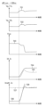
- FIG. 8 is a diagram schematically illustrating waveforms of voltages and currents actually measured in a first turn-on evaluation experiment according to an embodiment of the present disclosure.
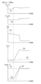
- FIG. 9 is a diagram schematically illustrating waveforms of voltages and currents actually measured in a second turn-on evaluation experiment according to an embodiment of the present disclosure;
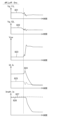
- FIG. 10 is a diagram schematically illustrating waveforms of voltages and currents actually measured in a third turn-on evaluation experiment according to an embodiment of the present disclosure;
- FIG. 11 is a diagram illustrating turn-on loss versus turn-on time difference between two transistors, according to an embodiment of the present disclosure.
- FIG. 12 is a diagram illustrating recovery loss versus turn-on time difference between two transistors, according to an embodiment of the present disclosure.
- FIG. 13 is a diagram schematically illustrating waveforms of voltages and currents actually measured in a first turn-off evaluation experiment according to an embodiment of the present disclosure;
- FIG. 14 is a diagram schematically illustrating waveforms of voltages and currents actually measured in a second turn-off evaluation experiment according to an embodiment of the present disclosure;
- FIG. 15 is a diagram schematically showing waveforms of voltages and currents actually measured in a third turn-off evaluation experiment according to an embodiment of the present disclosure;
- FIG. 16 is a diagram schematically illustrating waveforms of voltages and currents actually measured in a fourth turn-off evaluation experiment according to an embodiment of the present disclosure;
- FIG. 13 is a diagram schematically illustrating waveforms of voltages and currents actually measured in a first turn-off evaluation experiment according to an embodiment of the present disclosure
- FIG. 14 is a diagram schematically illustrating wave
- FIG. 17 is a diagram illustrating turn-off loss versus turn-off time difference between two transistors, according to an embodiment of the present disclosure.
- FIG. 18 is a diagram illustrating how a semiconductor device is provided with a plurality of half-bridge circuits according to an embodiment of the present disclosure.
- the ground refers to a reference conductive portion having a potential of 0 V (zero volt) as a reference, or refers to a potential of 0 V itself.
- the reference conductive portion is made of a conductor such as metal.
- a potential of 0 V is sometimes referred to as a ground potential.
- voltages shown without specific reference represent potentials with respect to ground.
- a level refers to a level of potential, and for any signal or voltage of interest, a high level has a higher potential than a low level.
- a high level For any signal or voltage of interest, strictly speaking that the signal or voltage is at a high level means that the signal or voltage is at a high level, and strictly speaking that the signal or voltage is at a low level. It means that the signal or voltage level is at low level.
- Levels for signals are sometimes referred to as signal levels, and levels for voltages are sometimes referred to as voltage levels.
- the switching from low level to high level is called up edge (or rising edge), and the timing of switching from low level to high level is called up edge timing (or rising edge timing).
- up edge timing or rising edge timing
- rising edge timing or rising edge timing
- falling edge timing or falling edge timing
- a period during which the level of the signal is high is called a high level period
- a period during which the level of the signal is low is called a low level period.
- the same is true for any voltage that takes a high or low voltage level.
- MOSFET Field Effect Transistor
- the ON state refers to the state in which there is conduction between the drain and source of the transistor
- the OFF state refers to the state in which there is conduction between the drain and source of the transistor. It refers to the state in which the current between the two is non-conducting (blocking state).
- MOSFETs are understood to be enhancement mode MOSFETs unless otherwise stated.
- MOSFET is an abbreviation for Metal-Oxide-Semiconductor Field-Effect Transistor.
- the back gate is understood to be shorted to the source.
- the electrical characteristics of a MOSFET include the gate threshold voltage.
- the gate threshold voltage For an N-channel MOSFET, when the gate potential of the MOSFET is higher than the source potential of the MOSFET and the magnitude of the gate-source voltage of the MOSFET is equal to or greater than the gate threshold voltage of the MOSFET, the MOSFET is It will be on, otherwise the MOSFET will be off.
- the gate-to-source voltage refers to the potential of the gate relative to the potential of the source.
- the on state refers to conduction between the transistor's collector and emitter
- the off state refers to non-conduction between the transistor's collector and emitter. It refers to the state (blocked state).
- IGBT is an abbreviation for Insulated Gate Bipolar Transistor.
- the electrical characteristics of IGBTs include the gate threshold voltage.
- the gate-emitter voltage refers to the potential of the gate as seen from the potential of the emitter.
- Connections between multiple parts forming a circuit such as arbitrary circuit elements, wirings, and nodes, may be understood to refer to electrical connections unless otherwise specified.
- FIG. 1 shows the overall configuration of the system SYS according to the first embodiment.
- System SYS can be referred to as a load driving system.
- the system SYS includes a semiconductor device 1 for driving a load LD, an MPU (Micro Processing Unit) 2, a voltage source 3, a capacitor CB, and a sense resistor Rs.
- the semiconductor device 1 can also be called a load driving device or a load driving semiconductor device.
- FIG. 2 is an external perspective view of the semiconductor device 1.
- the semiconductor device 1 includes a semiconductor chip having a semiconductor integrated circuit formed on a semiconductor substrate, a semiconductor discrete component, a housing (package) for housing the semiconductor chip and the semiconductor discrete component, and an exterior of the semiconductor device 1 from the housing. and a plurality of external terminals exposed to the electronic component.
- a semiconductor device 1 is formed by enclosing a semiconductor chip and semiconductor discrete components in a housing (package) made of resin. This type of semiconductor device 1 can be called IPM (Intelligent Power Modules).
- IPM Intelligent Power Modules
- the number of external terminals of the semiconductor device 1 and the type of housing of the semiconductor device 1 shown in FIG. 2 are merely examples, and they can be designed arbitrarily.
- terminals TM11 to TM17 are shown in FIG.
- a terminal TM11 is an output terminal to which an output terminal voltage Vsw is applied.
- a terminal TM12 is a power supply terminal to which a power supply voltage VP is applied.
- Terminal TM13 is a low-side terminal.
- a terminal TM14 is a ground terminal connected to the ground.
- a terminal TM15 is a boot terminal to which a boot voltage VB is applied.
- a terminal TM16 is a control input terminal to which a drive control signal HIN is applied.
- a terminal TM17 is a control input terminal to which a drive control signal LIN is applied. Drive control signals HIN and LIN are input control signals for the semiconductor device 1 .
- the load LD is connected to the output terminal TM11 and driven based on power supplied through the output terminal TM11.
- Load LD includes an inductive load.
- one end of the coil as the load LD is connected to the output terminal TM11, and the other end of the coil as the load LD is connected to the wiring to which the power supply voltage VP is applied.
- the load LD may be a motor coil (armature winding).
- the load LD is arbitrary as long as it includes an inductive load.
- a current flowing between the output terminal TM11 and the load LD is hereinafter referred to as a load current, and the load current is referred to by the symbol "Io".
- a capacitor CB is a bootstrap capacitor provided outside the semiconductor device 1 . Outside the semiconductor device 1, the capacitor CB is provided between the terminals TM11 and TM15. That is, one end of the capacitor CB is connected to the output terminal TM11, and the other end of the capacitor CB is connected to the boot terminal TM15. A modification in which the capacitor CB is incorporated in the semiconductor device 1 is also possible.
- the voltage source 3 outputs a power supply voltage VP having a predetermined positive DC voltage value.
- the power supply voltage VP may also be called a power supply voltage.
- a power supply voltage VP is input to a power supply terminal TM12.
- the voltage value of the power supply voltage VP is arbitrary. For example, the power supply voltage VP is several hundred V (volts).
- the low-side terminal TM13 is connected to the ground via the sense resistor Rs.
- a modification in which the sense resistor Rs is built in the semiconductor device 1 is also possible.
- the low-side terminal TM13 may be directly connected to the ground.
- an overcurrent protection operation for a switching element 10H or 10L, which will be described later, can be performed based on the voltage drop of the sense resistor Rs.
- it is also possible to omit the sense resistor Rs in the system SYS it is also possible to omit the sense resistor Rs in the system SYS (it may be understood that the resistance value of the sense resistor Rs is 0 ⁇ ).
- the MPU 2 generates and outputs drive control signals HIN and LIN.
- the drive control signal HIN is input to the control input terminal TM16
- the drive control signal LIN is input to the control input terminal TM17.
- Each of the drive control signals HIN and LIN is a digital signal (binary signal) that takes either a high level or a low level.
- High levels of the drive control signals HIN and LIN match the level of the power supply voltage VCC2 of the MPU 2
- low levels of the drive control signals HIN and LIN match the ground level (see FIG. 3).
- Matching here is a concept that also includes substantially matching.
- the voltage value of power supply voltage VCC2 is arbitrary. For example, the power supply voltage VCC2 is 5V (volt).
- the semiconductor device 1 includes a high-side switching element 10H and a low-side switching element 10L, a high-side driver 20H and a low-side driver 20L, a boot circuit 30, gate resistors 41H, 42H, 41L and 42L, Prepare.
- the switching elements 10H and 10L are composite switching elements each having a parallel connection circuit of a field effect transistor and an insulated gate bipolar transistor.
- the switching element 10H includes a transistor 11H that is an N-channel MOSFET, a transistor 12H that is an N-channel IGBT, and a diode 13H that is a Schottky barrier diode.
- Transistors 11H and 12H and diode 13H can be formed of semiconductor discrete components.
- Diode 11Hd represents a parasitic diode added to transistor 11H.
- the switching element 10H has terminals 15H and 16H.
- the drain of transistor 11H, the collector of transistor 12H and the cathode of diode 13H are commonly connected to terminal 15H.
- the source of transistor 11H, the emitter of transistor 12H and the anode of diode 13H are commonly connected to terminal 16H.
- the anode and cathode of the parasitic diode 11Hd are connected to the source and drain of the transistor 11H, respectively.
- the switching element 10L includes a transistor 11L that is an N-channel MOSFET, a transistor 12L that is an N-channel IGBT, and a diode 13L that is a Schottky barrier diode.
- Transistors 11L and 12L and diode 13L can be formed of semiconductor discrete components.
- Diode 11Ld represents a parasitic diode added to transistor 11L.
- the switching element 10L has terminals 15L and 16L.
- the drain of transistor 11L, the collector of transistor 12L and the cathode of diode 13L are commonly connected to terminal 15L.
- the source of transistor 11L, the emitter of transistor 12L and the anode of diode 13L are commonly connected to terminal 16L.
- the anode and cathode of the parasitic diode 11Ld are connected to the source and drain of the transistor 11L, respectively.
- the terminal 15H is connected to the power supply terminal TM12 to receive the power supply voltage VP.
- the terminal 16L is connected to the low side terminal TM13.
- Terminals 16H and 15L are connected to each other within semiconductor device 1 .
- Terminals 16H and 15L are connected to output terminal TM11.
- the switching elements 10H and 10L are connected in series to form a half bridge circuit.
- the switching element 10H makes the terminals 15H and 16H conductive or non-conductive under the control of the high side driver 20H.
- a state in which the terminals 15H and 16H are conductive is referred to as an ON state of the switching element 10H, and a state in which the terminals 15H and 16H are non-conductive is referred to as an OFF state of the switching element 10H.
- switching element 10H is on.
- the switching element 10H is also on when one of the transistors 11H and 12H is on and the other is off. When both transistors 11H and 12H are off, switching element 10H is off.
- the switching element 10L makes the terminals 15L and 16L conductive or non-conductive under the control of the low-side driver 20L.
- a state in which the terminals 15L and 16L are electrically connected is referred to as an ON state of the switching element 10L, and a state in which the terminals 15L and 16L are not electrically connected is referred to as an OFF state of the switching element 10L.
- the switching element 10L is on.
- the switching element 10L is also in the ON state when one of the transistors 11L and 12L is in the ON state and the other is in the OFF state. When both transistors 11L and 12L are off, switching element 10L is off.
- the transistors 11H and 11L are formed using silicon carbide (SiC). However, it is also possible to form transistors 11H and 11L using a semiconductor material other than silicon carbide (eg, silicon). Transistors 12H and 12L may be formed using silicon (Si). Diodes 13H and 13L are formed using silicon carbide (SiC). However, it is also possible to form the diodes 13H and 13L using a semiconductor material other than silicon carbide (eg, silicon).
- the on state and off state of any transistor or switching element may be simply expressed as on and off.
- switching from an off state to an on state is expressed as turn-on
- switching from an on state to an off state is expressed as turn-off.
- the timing at which turn-on occurs and the timing at which turn-off occurs are expressed as turn-on timing and turn-off timing, respectively.
- the period during which the transistor or switching element is on may be referred to as an on period
- the period during which the transistor or switching element is off may be referred to as an off period. be.
- the drive control signal HIN received at the control input terminal TM16 is input to the high side driver 20H.
- the high side driver 20H is connected to the ground, and the control power supply voltage VCC, the output terminal voltage Vsw and the boot voltage VB are input to the high side driver 20H.
- the high-side driver 20H drives the switching element 10H (controls the state of the switching element 10H) by controlling the gate potentials of the transistors 11H and 12H according to the drive control signal HIN.
- the control power supply voltage VCC is a positive DC voltage (eg, 15V) supplied to the semiconductor device 1 from an external power supply (not shown). Alternatively, the semiconductor device 1 may generate the control power supply voltage VCC.
- the drive control signal LIN received at the control input terminal TM17 is input to the low-side driver 20L. Also, the low side driver 20L is connected to the ground, and the control power supply voltage VCC is input to the low side driver 20L.
- the low-side driver 20L drives the switching element 10L (controls the state of the switching element 10L) by controlling the gate potentials of the transistors 11L and 12L according to the drive control signal LIN.
- a boot voltage VB is generated at the boot terminal TM15 by a bootstrap circuit composed of the circuit 30 for booting and the capacitor CB.
- the boot circuit 30 is provided with a diode 31 having an anode for receiving the control power supply voltage VCC and a cathode connected to the boot terminal TM15.
- a diode 31 having an anode for receiving the control power supply voltage VCC and a cathode connected to the boot terminal TM15.
- the gate voltage of the transistor 11H (that is, the voltage applied to the gate of the transistor 11H) is referred to by the symbol "Vg_11H".
- the gate voltage of transistor 12H (ie, the voltage applied to the gate of transistor 12H) is referenced by the symbol "Vg_12H”.
- Two wirings 43H and 44H separated from each other are provided between the high side driver 20H and the switching element 10H.
- One end of the wiring 43H is connected to the high side driver 20H, and the other end of the wiring 43H is connected to the gate of the transistor 11H.
- the high-side driver 20H outputs charges (positive charges) to the wiring 43H or draws charges (positive charges) from the wiring 43H to control the gate voltage Vg_11H, thereby controlling the state (on, off) of the transistor 11H.
- a gate resistor 41H is inserted in series on the wiring 43H. However, the gate resistor 41H may be built in the high side driver 20H. Gate resistor 41H may be omitted.
- One end of the wiring 44H is connected to the high side driver 20H, and the other end of the wiring 44H is connected to the gate of the transistor 12H.
- the high-side driver 20H outputs charge (positive charge) to the wiring 44H or draws charge (positive charge) from the wiring 44H to control the gate voltage Vg_12H, thereby controlling the state (on, off) of the transistor 12H. ).
- a gate resistor 42H is inserted in series on the wiring 44H. However, the gate resistor 42H may be built in the high side driver 20H. Gate resistor 42H may be omitted.
- the gate voltage of the transistor 11L (that is, the voltage applied to the gate of the transistor 11L) is referred to by the symbol "Vg_11L”.
- the gate voltage of transistor 12L (ie, the voltage applied to the gate of transistor 12L) is referenced by the symbol "Vg_12L”.
- Two wirings 43L and 44L separated from each other are provided between the low-side driver 20L and the switching element 10L.
- One end of the wiring 43L is connected to the low side driver 20L, and the other end of the wiring 43L is connected to the gate of the transistor 11L.
- the low-side driver 20L outputs charge (positive charge) to the wiring 43L or draws charge (positive charge) from the wiring 43L to control the gate voltage Vg_11L, thereby controlling the state (on, off) of the transistor 11L. to control.
- a gate resistor 41L is inserted in series on the wiring 43L. However, the gate resistor 41L may be built in the low side driver 20L. Gate resistor 41L may be omitted.
- One end of the wiring 44L is connected to the low side driver 20L, and the other end of the wiring 44L is connected to the gate of the transistor 12L.
- the low-side driver 20L outputs charge (positive charge) to the wiring 44L or draws charge (positive charge) from the wiring 44L to control the gate voltage Vg_12L, thereby controlling the state (on, off) of the transistor 12L. to control.
- a gate resistor 42L is inserted in series on the wiring 44L. However, the gate resistor 42L may be built in the low side driver 20L. Gate resistor 42L may be omitted.
- Fig. 3 shows the relationship between each drive control signal, each gate voltage and the state of each transistor.
- the high-side driver 20H generates and controls gate voltages Vg_11H and Vg_12H based on the voltage between terminals TM11 and TM15, that is, based on the differential voltage (VB-Vsw).
- the high-side driver 20H can individually set the gate voltages Vg_11H and Vg_12H to high level or low level according to the drive control signal HIN.
- the high level of the gate voltages Vg_11H and Vg_12H has the level of the boot voltage VB
- the low level of the gate voltages Vg_11H and Vg_12H has the level of the output terminal voltage Vsw.
- the voltage (VB-Vsw) represents the differential voltage between the terminals TM11 and TM15 with the potential of the terminal TM11 as a reference, and corresponds to the height of the boot voltage VB seen from the output terminal voltage Vsw.
- the boot voltage VB is higher than the output terminal voltage Vsw, and in steady state, the difference voltage (VB-Vsw) is stabilized at or near the control power supply voltage VCC (i.e., the difference voltage (VB -Vsw) is stabilized at the same level as the value of the control power supply voltage VCC).
- the magnitude of the control power supply voltage VCC is greater than the magnitude of each gate threshold voltage of the transistors 11H and 12H.
- the transistor 11H is turned on during the high level period of the gate voltage Vg_11H, and turned off during the low level period of the gate voltage Vg_11H.
- the transistor 12H is turned on during the high level period of the gate voltage Vg_12H, and turned off during the low level period of the gate voltage Vg_12H.
- the low-side driver 20L generates and controls gate voltages Vg_11L and Vg_12L based on the control power supply voltage VCC.
- the low-side driver 20L can individually set the gate voltages Vg_11L and Vg_12L to high level or low level according to the drive control signal LIN.
- a high level at the gate voltages Vg_11L and Vg_12L has the level of the control power supply voltage VCC, and a low level at the gate voltages Vg_11L and Vg_12L has the ground level (ie ground potential).
- the magnitude of the control power supply voltage VCC is greater than the magnitude of each gate threshold voltage of the transistors 11L and 12L. Therefore, the transistor 11L is turned on during the high level period of the gate voltage Vg_11L, and turned off during the low level period of the gate voltage Vg_11L. Similarly, the transistor 12L is turned on during the high level period of the gate voltage Vg_12L, and turned off during the low level period of the gate voltage Vg_12L.
- any voltage of interest that takes a high level or a low level includes that the level of the voltage of interest matches the specific level.
- Another concept involves the level of the voltage of interest substantially matching a particular level. Therefore, for example, although the high level gate voltage Vg_11H is equivalent to the level of the boot voltage VB, strictly speaking, it may be slightly different from the level of the boot voltage VB. The same is true for any signal that takes a high level or a low level.
- MOSFETs have the characteristic of being able to keep steady-state loss low for small currents compared to IGBTs
- IGBTs have the characteristic of being able to keep steady-state losses low for large currents compared to MOSFETs. Therefore, by forming a switching element using a parallel connection circuit of a MOSFET and an IGBT, it is possible to keep the steady-state loss low over a wide current range. Simply, it is conceivable to simultaneously turn on/off the MOSFET and the IGBT in synchronization with the drive control signal (HIN or LIN). However, turning on and off the MOSFET and IGBT at the same time is not always optimal for reducing switching loss.
- the low-side driver 20L when the low-side driver 20L turns on the switching element 10L in synchronization with the rising edge of the drive control signal LIN, one of the transistors 11L and 12L can be turned on first and then the other. can.
- the low-side driver 20L turns off the switching element 10L in synchronization with the down edge of the drive control signal LIN, it can first turn off one of the transistors 11L and 12L and then turn off the other.
- the high side driver 20H In the example of FIG. 3, when the switching element 10L is turned on, the transistor 11L is turned on first, but the transistor 12L may be turned on first. In the example of FIG. 3, when the switching element 10L is turned off, the transistor 11L is turned off first, but the transistor 12L may be turned off first. The same applies to the high side driver 20H.
- Fig. 4 shows the internal configuration of the drivers 20H and 20L.
- the high side driver 20H has parts referenced 21H to 29H.
- the low-side driver 20L has parts referenced by reference numerals 21L to 26L.
- the input circuit 21H operates based on the power supply voltage VCC2 (eg, 5V) with reference to the ground potential.
- the input circuit 21H consists of a Schmidt buffer and outputs a binarized signal 611 obtained by waveform-shaping the drive control signal HIN.
- the level shifter 22H generates a binarized signal 612 by level-shifting the binarized signal 611 based on the power supply voltage VCC2 (eg, 5V) and the control power supply voltage VCC (eg, 15V). Any binarized signal has a low level or a high level signal level.
- the high level of binarized signal 611 has the level of power supply voltage VCC2, while the high level of binarized signal 612 has the level of control power supply voltage VCC.
- the low level of binarized signals 611 and 612 has a ground level.
- the power supply voltage VCC2 may be generated based on the control power supply voltage VCC.
- the pulse generation circuit 23H generates and outputs a set signal 613s and a reset signal 613r based on the binarized signal 612. Signals 613s and 613r in principle have a low level.
- the pulse generation circuit 23H sets the set signal 613s to a high level for a predetermined minute time at the rising edge timing of the binarized signal 612, and sets the reset signal 613r to a high level for a predetermined minute time at the falling edge timing of the binarized signal 612. High level.
- the high level of signals 613s and 613r has the level of control power supply voltage VCC.
- the low levels of signals 613s and 613r have a ground level.
- the level shifter 24H shifts the level of the set signal 613s based on the control power supply voltage VCC seen from the ground and the boot voltage VB seen from the output terminal voltage Vsw to generate the set signal 614s and the level of the reset signal 613r.
- the shift produces a reset signal 614r.
- Signals 614s and 614r essentially have a high level.
- the level shifter 24H sets the set signal 614s to low level only during the high level period of the set signal 613s, and sets the reset signal 614r to low level only during the high level period of the reset signal 613r.
- the high level of signals 614s and 614r has the level of boot voltage VB.
- the low level of signals 614s and 614r has the level of output terminal voltage Vsw.
- the filter 25H performs filtering to reduce noise in the set signal 614s and the reset signal 614r, and outputs the filtered set signal 614s as the set signal 615s and the filtered reset signal 614r as the reset signal 615r.
- the filter 25H may employ a low-active circuit configuration or a high-active circuit configuration. In the configuration example of FIG. 4, when the set signal 614s is at low level, the set signal 615s is also at low level, and when the set signal 614s is at high level, the set signal 615s is also at high level. Similarly, in the configuration example of FIG. 4, when the reset signal 614r is low level, the reset signal 615r is also low level, and when the reset signal 614r is high level, the reset signal 615r is also high level.
- a set signal 615s and a reset signal 615r are input to the latch circuit 26H composed of an RS-type flip-flop.
- the latch circuit 26H outputs a control signal CNT_H based on the set signal 615s and the reset signal 615r.
- the control signal CNT_H is a kind of binarized signal.
- a low active type circuit configuration may be employed in the latch circuit 26H, or a high active type circuit configuration may be employed.
- the latch circuit 26H causes the control signal CNT_H to generate a rising edge in synchronization with the falling edge of the set signal 615s, and then causes the control signal CNT_H to generate a falling edge in synchronization with the falling edge of the reset signal 615r.
- the latch circuit 26H operates using the boot voltage VB as the high potential side power supply voltage and the output terminal voltage Vsw as the low potential side power supply voltage. Therefore, the high level of the control signal CNT_H has the level of the boot voltage VB, and the low level of the control signal CNT_H has the level of the output terminal voltage Vsw (see FIG. 5).
- the control signal CNT_H corresponds to a signal obtained by level-shifting the drive control signal HIN. Assuming that the signal delay from the drive control signal HIN to the generation of the control signal CNT_H is zero, the control signal CNT_H is at the high level during the high level period of the drive control signal HIN, and the drive control signal HIN is at the low level. During the period, the control signal CNT_H becomes low level (see FIG. 5).
- a protection circuit (not shown) is incorporated in the latch circuit 26H, and the latch circuit 26H fixes the control signal CNT_H at low level when a predetermined abnormality (for example, the boot voltage VB is too low) is detected.
- the delay circuit 27H and the output circuits 28H and 29H also operate using the boot voltage VB as the high potential side power supply voltage and the output end voltage Vsw as the low potential side power supply voltage, similarly to the latch circuit 26H.
- the delay circuit 27H generates control signals CNT_11H and CNT_12H based on the control signal CNT_H.
- FIG. 5 shows the relationship between the drive control signal HIN and the control signals CNT_H, CNT_11H and CNT_12H.
- Each of the control signals CNT_11H and CNT_12H is also a kind of binarized signal. High levels of the control signals CNT_11H and CNT_12H have the level of the boot voltage VB, and low levels of the control signals CNT_11H and CNT_12H have the level of the output terminal voltage Vsw.
- the delay circuit 27H also causes the control signals CNT_11H and CNT_12H to rise in response to the rising edge of the control signal CNT_H.
- a rising edge of the control signal CNT_11H indicates turning on of the transistor 11H
- a rising edge of the control signal CNT_12H indicates turning on of the transistor 12H.
- the timing t_H1 of the rising edge of the control signal CNT_11H in response to the rising edge of the control signal CNT_H is simultaneous with or after the rising edge timing of the control signal CNT_H.
- a delay of the up edge timing t_H1 of the control signal CNT_11H from the up edge timing of the control signal CNT_H is referred to as a delay amount ⁇ d_H1.
- the timing t_H2 of the rising edge of the control signal CNT_12H in response to the rising edge of the control signal CNT_H is simultaneous with or after the rising edge timing of the control signal CNT_H.
- a delay of the up edge timing t_H2 of the control signal CNT_12H as viewed from the up edge timing of the control signal CNT_H is called a delay amount ⁇ d_H2.
- the delay amounts ⁇ d_H1 and ⁇ d_H2 may be different from each other. It may be " ⁇ d_H1> ⁇ d_H2" or " ⁇ d_H1 ⁇ d_H2". Only one of the delay amounts ⁇ d_H1 and ⁇ d_H2 may be zero.
- dff_Hon ⁇ 0 the transistor 12H is turned on earlier than the transistor 11H is turned on by the time corresponding to the absolute value
- the delay circuit 27H also causes the control signals CNT_11H and CNT_12H to have down edges in response to the down edge of the control signal CNT_H.
- a falling edge of the control signal CNT_11H indicates turning off of the transistor 11H
- a falling edge of the control signal CNT_12H indicates turning off of the transistor 12H.
- the timing t_H3 of the down edge of the control signal CNT_11H in response to the down edge of the control signal CNT_H is simultaneous with or after the down edge timing of the control signal CNT_H.
- a delay of the down edge timing t_H3 of the control signal CNT_11H from the down edge timing of the control signal CNT_H is referred to as a delay amount ⁇ d_H3.
- Timing t_H4 of the down edge of control signal CNT_12H in response to the down edge of control signal CNT_H is simultaneous with or after the down edge timing of control signal CNT_H.
- a delay of the down edge timing t_H4 of the control signal CNT_12H from the down edge timing of the control signal CNT_H is referred to as a delay amount ⁇ d_H4.
- the delay amounts ⁇ d_H3 and ⁇ d_H4 may be different from each other. It may be " ⁇ d_H3> ⁇ d_H4" or " ⁇ d_H3 ⁇ d_H4". Only one of the delay amounts ⁇ d_H3 and ⁇ d_H4 may be zero.
- the difference dff_Hoff represents the time difference between the timing at which the turn-off of the transistor 11H is instructed and the timing at which the turn-off of the transistor 12H is instructed.
- dff_Hoff ⁇ 0 the transistor 12H is turned off earlier than the transistor 11H is turned off by the time corresponding to the absolute value
- the transistor 11H is turned off earlier than the transistor 12H is turned off by the time corresponding to the absolute value
- the output circuit 28H is connected to a wiring 43H connected to the gate of the transistor 11H (see also FIG. 1).
- the output circuit 28H controls the gate voltage Vg_11H based on the control signal CNT_11H. Specifically, the output circuit 28H turns on the transistor 11H by setting the gate voltage Vg_11H to the level of the boot voltage VB during the high level period of the control signal CNT_11H, and maintains the gate voltage Vg_11H during the low level period of the control signal CNT_11H.
- the level of the output terminal voltage Vsw turns off the transistor 11H.
- the output circuit 28H receives the rising edge of the control signal CNT_11H and starts raising the gate voltage Vg_11H from the level of the output terminal voltage Vsw. Therefore, there is a delay from the rising edge of control signal CNT_11H to the actual turn-on of transistor 11H.
- the output circuit 28H receives the falling edge of the control signal CNT_11H and starts lowering the gate voltage Vg_11H from the level of the boot voltage VB. Therefore, there is a delay from the falling edge of control signal CNT_11H to the actual turning off of transistor 11H.
- the output circuit 29H is connected to a wiring 44H connected to the gate of the transistor 12H (see also FIG. 1).
- the output circuit 29H controls the gate voltage Vg_12H based on the control signal CNT_12H. Specifically, the output circuit 29H turns on the transistor 12H by setting the gate voltage Vg_12H to the level of the boot voltage VB during the high level period of the control signal CNT_12H. The level of the output terminal voltage Vsw turns off the transistor 12H. However, in detail, the output circuit 29H receives the rising edge of the control signal CNT_12H and starts raising the gate voltage Vg_12H from the level of the output terminal voltage Vsw.
- control signal CNT_12H there is a delay from the rising edge of control signal CNT_12H to the actual turn-on of transistor 12H.
- the output circuit 29H receives the falling edge of the control signal CNT_12H and starts lowering the gate voltage Vg_12H from the level of the boot voltage VB. Therefore, there is a delay from the falling edge of control signal CNT_12H to the actual turning off of transistor 12H.
- the configuration of the low-side driver 20L will be described with reference to FIG.
- the input circuit 21L, the control logic circuit 22L, and the delay circuit 23L operate based on the power supply voltage VCC2 with reference to the ground potential.
- the input circuit 21L consists of a Schmidt buffer and outputs a binarized signal 621 obtained by waveform shaping the drive control signal LIN.
- the control logic circuit 22L generates the control signal CNT_L based on the binarized signal 621.
- the control signal CNT_L is a kind of binarized signal.
- the drive control signal LIN, the binarized signal 621, and the control signal CNT_L may be understood to be substantially the same rectangular wave signal.
- the control logic circuit 22L has a built-in protection circuit (not shown), and when an abnormality (such as a temperature abnormality or an overcurrent abnormality) is detected in the protection circuit, the control signal CNT_L is maintained at a low level. be done.
- an abnormality such as a temperature abnormality or an overcurrent abnormality
- the delay circuit 23L generates control signals CNT_11L and CNT_12L based on the control signal CNT_L.
- FIG. 6 shows the relationship between the drive control signal LIN and the control signals CNT_L, CNT_11L and CNT_12L.
- Each of the control signals CNT_11L and CNT_12L is also a kind of binarized signal. Similar to the drive control signal LIN, the high levels of the control signals CNT_L, CNT_11L and CNT_12L have the level of the power supply voltage VCC2, and the low levels of the control signals CNT_L, CNT_11L and CNT_12L have the ground level.
- the delay circuit 23L also causes the control signals CNT_11L and CNT_12L to rise in response to the rising edge of the control signal CNT_L.
- a rising edge of the control signal CNT_11L indicates turning on of the transistor 11L
- a rising edge of the control signal CNT_12L indicates turning on of the transistor 12L.
- the timing t_L1 of the rising edge of the control signal CNT_11L in response to the rising edge of the control signal CNT_L is simultaneous with or after the rising edge timing of the control signal CNT_L.
- a delay of the up edge timing t_L1 of the control signal CNT_11L as viewed from the up edge timing of the control signal CNT_L is called a delay amount ⁇ d_L1.
- the up edge timing t_L2 of the control signal CNT_12L in response to the up edge of the control signal CNT_L is the same as or after the up edge timing of the control signal CNT_L.
- a delay of the up edge timing t_L2 of the control signal CNT_12L from the up edge timing of the control signal CNT_L is referred to as a delay amount ⁇ d_L2.
- the delay amounts ⁇ d_L1 and ⁇ d_L2 may be different from each other. " ⁇ d_L1> ⁇ d_L2" or " ⁇ d_L1 ⁇ d_L2". Only one of the delay amounts ⁇ d_L1 and ⁇ d_L2 may be zero.
- the difference dff_Lon represents the time difference between the timing at which the turn-on of the transistor 11L is instructed and the timing at which the turn-on of the transistor 12L is instructed.
- dff_Lon ⁇ 0 the transistor 12L is turned on earlier than the transistor 11L is turned on by the time corresponding to the absolute value
- the transistor 11L is turned on earlier than the transistor 12L is turned on by the time corresponding to the absolute value
- the delay circuit 23L also causes the control signals CNT_11L and CNT_12L to have down edges in response to the down edge of the control signal CNT_L.
- a falling edge of the control signal CNT_11L indicates turning off of the transistor 11L
- a falling edge of the control signal CNT_12L indicates turning off of the transistor 12L.
- the timing t_L3 of the down edge of the control signal CNT_11L in response to the down edge of the control signal CNT_L is simultaneous with or after the down edge timing of the control signal CNT_L.
- a delay of the down edge timing t_L3 of the control signal CNT_11L from the down edge timing of the control signal CNT_L is referred to as a delay amount ⁇ d_L3.
- the down edge timing t_L4 of the control signal CNT_12L in response to the down edge of the control signal CNT_L is the same as or after the down edge timing of the control signal CNT_L.
- a delay of the down edge timing t_L4 of the control signal CNT_12L from the down edge timing of the control signal CNT_L is referred to as a delay amount ⁇ d_L4.
- the delay amounts ⁇ d_L3 and ⁇ d_L4 may be different from each other. " ⁇ d_L3> ⁇ d_L4" or " ⁇ d_L3 ⁇ d_L4". Only one of the delay amounts ⁇ d_L3 and ⁇ d_L4 may be zero.
- the difference dff_Loff represents the time difference between the timing at which the turn-off of the transistor 11L is instructed and the timing at which the turn-off of the transistor 12L is instructed.
- dff_Loff ⁇ 0 the transistor 12L is turned off earlier than the transistor 11L is turned off by the time corresponding to the absolute value
- the transistor 11L is turned off earlier than the transistor 12L is turned off by the time corresponding to the absolute value
- the level shifter 24L generates control signals CNT_11L' and CNT_12L' by level-shifting the control signals CNT_11L and CNT_12L based on the power supply voltage VCC2 (eg, 5V) and the control power supply voltage VCC (eg, 15V).
- the level shift by the level shifter 24L shifts the high level of the control signals CNT_11L and CNT_12L to the level of the control power supply voltage VCC.
- the control signals CNT_11L and CNT_12L after the shift are control signals CNT_11L' and CNT_12L', respectively.
- the output circuit 25L is connected to a wiring 43L connected to the gate of the transistor 11L (see also FIG. 1).
- the output circuit 25L controls the gate voltage Vg_11L based on the control signal CNT_11L'. Specifically, the output circuit 25L turns on the transistor 11L by setting the gate voltage Vg_11L to the level of the control power supply voltage VCC during the high level period of the control signal CNT_11L', and turns on the gate voltage during the low level period of the control signal CNT_11L'.
- the transistor 11L is turned off by setting the voltage Vg_11L to the ground level. More specifically, however, the output circuit 25L receives the rising edge of the control signal CNT_11L' and starts raising the gate voltage Vg_11L from the ground level.
- the output circuit 25L receives the falling edge of the control signal CNT_11L' and starts lowering the gate voltage Vg_11L from the level of the control power supply voltage VCC. Therefore, there is a delay from the falling edge of the control signal CNT_11L' until the transistor 11L is actually turned off.
- the output circuit 26L is connected to a wiring 44L connected to the gate of the transistor 12L (see also FIG. 1).
- the output circuit 26L controls the gate voltage Vg_12L based on the control signal CNT_12L'. Specifically, the output circuit 26L turns on the transistor 12L by setting the gate voltage Vg_12L to the level of the control power supply voltage VCC during the high level period of the control signal CNT_12L', and turns on the gate voltage during the low level period of the control signal CNT_12L'.
- the transistor 12L is turned off by grounding the voltage Vg_12L.
- the output circuit 26L receives the rising edge of the control signal CNT_12L' and starts raising the gate voltage Vg_12L from the ground level.
- control signal CNT_12L' there is a delay from the rising edge of control signal CNT_12L' to the actual turn-on of transistor 12L.
- the output circuit 26L receives the falling edge of the control signal CNT_12L' and starts lowering the gate voltage Vg_12L from the level of the control power supply voltage VCC. Therefore, there is a delay from the falling edge of control signal CNT_12L' to the actual turning off of transistor 12L.
- the amount of delay (the amount of delay in the delay circuit) suitable for reducing switching loss
- the gate and source of the transistor 11H are shorted and the gate and emitter of the transistor 12H are shorted.
- An evaluation experiment was conducted using the evaluation system shown in FIG. In the evaluation experiment, the drive control signal LIN was alternately switched between high level and low level so that a substantially constant load current Io continued to flow from the wiring to which the power supply voltage VP was applied to the output terminal TM11 via the load LD. switched.
- the drain current Id of the transistor 11L and the collector current Ic of the transistor 12L were actually measured in the evaluation experiment. Also, the sum of the drain current Id of the transistor 11L and the collector current Ic of the transistor 12L is called a sum current Imath.
- FIGS. 8, 9, and 10 schematically show waveforms of voltages and currents actually measured in the first, second, and third turn-on evaluation experiments, respectively.
- the time difference dff_Lon was set to "-300 ns". This approximately corresponds to turning on transistor 12L earlier than transistor 11L by 300 ns.
- the time difference dff_Lon was set to "+100 ns”. This approximately corresponds to turning on the transistor 11L earlier than the transistor 12L by 100 ns.
- the time difference dff_Lon was set to "+500 ns". This approximately corresponds to turning on transistor 11L earlier than transistor 12L by 500 ns. Note that "ns” is an abbreviation for nanoseconds.
- waveforms 711, 712, 713, 714, 715, 716, and 717 are respectively the gate voltage Vg_11L, the gate voltage Vg_12L, the output terminal voltage Vsw, the drain current Id, the collector current Ic, and the sum in the first turn-on evaluation experiment.
- Schematic waveforms of current Imath and load current Io are shown.
- waveforms 721, 722, 723, 724, 725, 726, and 727 are respectively the gate voltage Vg_11L, the gate voltage Vg_12L, the output terminal voltage Vsw, the drain current Id, the collector current Ic, and the sum in the second turn-on evaluation experiment.
- Schematic waveforms of current Imath and load current Io are shown.
- waveforms 731, 732, 733, 734, 735, 736, and 737 are respectively the gate voltage Vg_11L, the gate voltage Vg_12L, the output terminal voltage Vsw, the drain current Id, the collector current Ic, and the sum in the third turn-on evaluation experiment.
- Schematic waveforms of current Imath and load current Io are shown.
- 8 to 10 are derived from the current flowing on the board used for evaluation and the inductance component of the pattern on the board (see FIGS. 13 to 16 to be described later). as well).
- the waveforms shown in FIGS. 8 to 10 are schematic representations of the actually measured waveforms, and the noise components contained in the actually measured waveforms are not shown in FIGS. The same is true for ).
- the dashed straight line 718 in FIG. 8, the dashed straight line 728 in FIG. 9, and the dashed straight line 738 in FIG. represents the slope of the sum current Imath at .
- the increase rate of the sum current Imath changes abruptly in the process of increasing the sum current Imath accompanying the turn-on of the switching element 10L.
- the transistor 12L since the transistor 12L is turned on first, the sum current Imath increases only by the increase in the collector current Ic, and then the transistor 11L is turned on, so that the increase rate of the sum current Imath increases. Because it does.
- the transistor 11L since the transistor 11L is turned on first, the sum current Imath increases only by the increase in the drain current Id, and then the transistor 12L is turned on, so that the increase rate of the sum current Imath increases. Because it does.
- the increase rate of the sum current Imath is kept substantially constant in the process of increasing the sum current Imath accompanying the turn-on of the switching element 10L. This means that the drain current Id and the collector current Ic increase at approximately the same rate and at the same time in the process of increasing the sum current Imath.
- the turn-on loss Eon is minimized under the condition that the rate of increase of the sum current Imath is kept substantially constant in the process of increasing the sum current Imath as the switching element 10L is turned on.
- waveform 760 shows the relationship between turn-on loss Eon and time difference dff_Lon in the turn-on evaluation experiment.
- a turn-on loss Eon is a switching loss when the switching element 10L is turned on. That is, the turn-on loss Eon is the loss generated in the switching element 10L when the switching element 10L transitions from the OFF state to the ON state.
- the turn-on loss Eon corresponds to the sum of the turn-on loss of the transistor 11L and the turn-on loss of the transistor 12L.
- the turn-on loss of the transistor 11L is switching loss that occurs in the transistor 11L when the transistor 11L transitions from an off state to an on state.
- the turn-on loss of the transistor 12L is switching loss that occurs in the transistor 12L when the transistor 12L transitions from the off state to the on state.
- waveform 770 shows the relationship between recovery loss Err and time difference dff_Lon in the turn-on evaluation experiment.
- the recovery loss Err is a recovery loss that occurs in the diodes 11Hd and 13H of the high side switching element 10H when the low side switching element 10 is turned on (this recovery loss occurs mainly in the diode 13H).
- 11 and 12 do not show specific numerical values of the turn-on loss Eon and the recovery loss Err, but the recovery loss Err is sufficiently smaller than the turn-on loss Eon (for example, 1/10 to several 10 minutes). ). Therefore, when discussing the total switching loss of the switching elements 10H and 10L, it can be said that attention should be paid only to the turn-on loss Eon.
- the turn-on loss Eon can be minimized by setting the time difference dff_Lon to approximately "+100 ns".
- is considerably large when the switching element 10L is turned on, the current flows only through one of the transistors 11L and 12L for a long period of time, leading to an increase in the turn-on loss Eon.
- the time difference dff_Lon is close to zero, the switching element 10L is turned on in such a manner that the currents are almost evenly distributed to the transistors 11L and 12L, so a reduction in the turn-on loss Eon can be expected.
- the time difference dff_Lon suitable for minimizing the turn-on loss Eon varies depending on the combination of characteristics of the transistors 11L and 12L.
- the semiconductor device 1 has a delay circuit 23L so that an arbitrary time difference dff_Lon can be provided between the turn-on timings of the transistors 11L and 12L.
- the time difference dff_Lon for minimizing the turn-on loss Eon should be determined through experiments or the like in the design stage, manufacturing stage, or shipping process of the semiconductor device 1, and the determined time difference dff_Lon should be adopted in the delay circuit 23L. .
- the delay circuit 23L reduces the switching loss (i.e., It is preferable to set the time difference dff_Lon so that the turn-on loss (Eon) is reduced.
- the delay circuit 23L is arranged so that the timing at which the rate of increase of the drain current Id of the transistor 11L is maximized and the timing at which the rate of increase of the collector current Ic of the transistor 12L is maximized coincide with each other. It is preferable to provide a time difference dff_Lon.
- the turn-on loss was evaluated by focusing on the low-side switching element 10L, and the configuration of the delay circuit 23L based on the evaluation results was described above, but the high-side delay circuit 27H is designed similarly.
- the delay circuit 27H reduces the switching loss at the turn-on of the switching element 10H (hereinafter referred to as It is preferable to set the time difference dff_Hon so that the turn-on loss Eon') is reduced.
- the delay circuit 27H provides a time difference dff_Hon so that the timing at which the rate of increase of the drain current of the transistor 11H is maximized and the timing at which the rate of increase of the collector current of the transistor 12H is maximized. and good.
- a turn-on loss Eon' is a loss generated in the switching element 10H when the switching element 10H transitions from an off state to an on state.
- the turn-on loss Eon' corresponds to the sum of the turn-on loss of transistor 11H and the turn-on loss of transistor 12H.
- the turn-on loss of the transistor 11H is switching loss that occurs in the transistor 11H when the transistor 11H transitions from an off state to an on state.
- the turn-on loss of the transistor 12H is switching loss that occurs in the transistor 12H when the transistor 12H transitions from the off state to the on state.
- FIGS. 13, 14, 15, and 16 schematically show waveforms of voltages and currents actually measured in the first, second, third, and fourth turn-off evaluation experiments, respectively.
- the time difference dff_Loff was set to "-200 ns". This approximately corresponds to turning off the transistor 12L earlier than the transistor 11L by 200 ns.
- the time difference dff_Loff was set to "0 ns”. This approximately corresponds to turning off transistors 11L and 12L at the same time.
- the time difference dff_Loff was set to "+300 ns".
- waveforms 811, 812, 813, 814, 815, 816, and 817 are respectively the gate voltage Vg_11L, the gate voltage Vg_12L, the output terminal voltage Vsw, the drain current Id, the collector current Ic, and the sum in the first turn-off evaluation experiment.
- Schematic waveforms of current Imath and load current Io are shown.
- waveforms 821, 822, 823, 824, 825, 826, and 827 are the gate voltage Vg_11L, the gate voltage Vg_12L, the output terminal voltage Vsw, the drain current Id, the collector current Ic, and the sum, respectively, in the second turn-off evaluation experiment.
- waveforms 831, 832, 833, 834, 835, 836, and 837 are respectively the gate voltage Vg_11L, the gate voltage Vg_12L, the output terminal voltage Vsw, the drain current Id, the collector current Ic, and the sum in the third turn-off evaluation experiment.
- waveforms of current Imath and load current Io are shown. In FIG.
- waveforms 841, 842, 843, 844, 845, 846, and 847 are the gate voltage Vg_11L, the gate voltage Vg_12L, the output terminal voltage Vsw, the drain current Id, the collector current Ic, and the sum, respectively, in the fourth turn-off evaluation experiment. Schematic waveforms of current Imath and load current Io are shown.
- the output terminal voltage Vsw When the switching element 10L is turned off, in the process of the transistor 11L or 12L transitioning from the ON state to the OFF state, the output terminal voltage Vsw once rises from around 0 V, drops, and then rises sharply (waveform 813, 823, 833 and 843).
- the first rise in the output terminal voltage Vsw occurs in the process of turning off the transistor 11L or 12L.
- the second rise in the output terminal voltage Vsw occurs in the process in which one of the transistors 11L and 12L turns off and then the other turns off, or in the process in which the transistors 11L and 12L simultaneously turn off. do.
- the turn-off loss Eoff increases (the turn-off loss Eoff will be described later). Therefore, shortening the length of the period as much as possible or to some extent is suitable for minimizing the turn-off loss Eoff. Also, the ratio of the currents flowing through the transistors 11L and 12L in the process of the switching element 10L transitioning from the ON state to the OFF state also affects the turn-off loss Eoff. Therefore, it is necessary to set the time difference dff_Loff in consideration of these to minimize the turn-off loss Eoff.
- waveform 860 shows the relationship between turn-off loss Eoff and time difference dff_Loff in the turn-off evaluation experiment.
- a turn-off loss Eoff is a switching loss when the switching element 10L is turned off. That is, the turn-off loss Eoff is loss generated in the switching element 10L when the switching element 10L transitions from the ON state to the OFF state.
- the turn-off loss Eoff corresponds to the sum of the turn-off loss of the transistor 11L and the turn-off loss of the transistor 12L.
- the turn-off loss of the transistor 11L is switching loss that occurs in the transistor 11L when the transistor 11L transitions from the ON state to the OFF state.
- the turn-off loss of the transistor 12L is switching loss that occurs in the transistor 12L when the transistor 12L transitions from the ON state to the OFF state.
- the turn-off loss Eoff can be minimized by setting the time difference dff_Loff to approximately "+300 ns".
- the time difference dff_Loff is "+300 ns" (see FIG. 15)
- the drain current Id of the transistor 11L decreases as the transistor 11L turns off first, and the collector current Id of the transistor 12H compensates for the decrease.
- Current Ic increases.
- the collector current Ic increases to some extent (in the process of increasing the collector current Ic)
- the transistor 12L transitions to the off state.
- the time difference dff_Loff suitable for minimizing the turn-off loss Eoff varies depending on the combination of characteristics of the transistors 11L and 12L.
- the semiconductor device 1 has a delay circuit 23L so that an arbitrary time difference dff_Loff can be provided between the turn-off timings of the transistors 11L and 12L.
- dff_Loff it is preferable to determine the time difference dff_Loff for minimizing the turn-off loss Eoff through experiments or the like in the design stage, manufacturing stage, or shipping process of the semiconductor device 1, and to adopt the determined time difference dff_Loff in the delay circuit 23L. .
- the delay circuit 23L reduces the switching loss (i.e., It is preferable to set the time difference dff_Loff so that the turn-off loss (Eoff) is reduced.
- a second predetermined change in the drive control signal LIN (here, When turning off the transistors 11L and 12L in response to the falling edge), the delay circuit 23L increases the collector current Ic of the transistor 12L by turning off the transistor 11L before the transistor 12L. It is preferable to set the time difference dff_Loff so that the transistor 12L is turned off when the ratio of the collector current Ic to the sum (Imath) of the drain current Id and the collector current Ic is equal to or less than a predetermined ratio.
- the predetermined percentage may be selected, for example, within the range of 50% to 95%.
- the turn-off loss was evaluated by focusing on the low-side switching element 10L, and the configuration of the delay circuit 23L based on the evaluation results was described above, but the high-side delay circuit 27H is similarly designed.
- the delay circuit 27H reduces the switching loss at the turn-off of the switching element 10H (hereinafter referred to as It is preferable to set the time difference dff_Hoff so that the turn-off loss Eoff') is reduced.
- delay circuit 27H causes transistor 11H to turn off before transistor 12H, thereby increasing the collector current of transistor 12H and then turning off transistor 11H.
- the time difference dff_Hoff may be set such that the transistor 12H turns off when the ratio of the collector current of the transistor 12H to the sum of the drain current and the collector current of the transistor 12H is less than or equal to a predetermined ratio.
- a turn-off loss Eoff' is a loss generated in the switching element 10H when the switching element 10H transitions from the ON state to the OFF state.
- the turn-off loss Eoff' corresponds to the sum of the turn-off loss of transistor 11H and the turn-off loss of transistor 12H.
- the turn-off loss of the transistor 11H is switching loss that occurs in the transistor 11H when the transistor 11H transitions from the ON state to the OFF state.
- the turn-off loss of the transistor 12H is switching loss that occurs in the transistor 12H when the transistor 12H transitions from the ON state to the OFF state.
- the switching elements 10H and 10L each have first to third elements.
- the first element is a transistor 11H or 11L composed of a MOSFET.
- the second element is a transistor 12H or 12L made up of an IGBT.
- a third element is a diode 13H or 13L connected in parallel to the first and second elements.
- the diode 13H or 13L is a Schottky barrier diode as described above. However, it is also possible to employ a PN junction diode as the diode 13H or 13L.
- the Schottky barrier diode as the diode 13H or 13L, the switching loss (Eon, Eon') at the time of turn-on in each switching element can be kept low, and the steady-state loss in the diode during regeneration can be kept low. can.
- the effect of suppressing these losses becomes remarkable when the transistors 11H and 11L and the diodes 13H and 13L are formed using silicon carbide (SiC).
- a second embodiment of the semiconductor device 1 will be described.
- a plurality of half bridge circuits may be provided by switching elements 10H and 10L.
- drivers 20H and 20L, boot circuit 30, gate resistors 41H, 42H, 41L and 42L, output terminal TM11, low side terminal TM13, boot terminal TM15, and control input terminal are provided for each half bridge circuit.
- TM16 and TM17 and capacitor CB may be provided.
- the gate resistance can be omitted (hereafter, the existence of the gate resistance is ignored).
- the semiconductor device 1 may be provided with a U-phase unit circuit, a V-phase unit circuit, and a W-phase unit circuit.
- Each unit circuit includes a half bridge circuit with switching elements 10H and 10L, drivers 20H and 20L, and a boot circuit 30.
- FIG. An output terminal TM11, a low-side terminal TM13, a boot terminal TM15, control input terminals TM16 and TM17, and a capacitor CB are provided for each unit circuit.
- the load LD in this case may be a three-phase motor having a U-phase coil, a V-phase coil and a W-phase coil.
- U-phase coil, the V-phase coil, and the W-phase coil are star-connected (Y-connected), one end of the U-phase coil, one end of the V-phase coil, and one end of the W-phase coil are connected to the output terminals for the U-phase, respectively.
- TM11, V-phase output terminal TM11, and W-phase output terminal TM11 are connected, and the other end of the U-phase coil, the other end of the V-phase coil, and the other end of the W-phase coil are connected in common.
- a high side driver 20H which is a driver circuit for the switching element 10H
- a low side driver 20L which is a driver circuit for the switching element 10L
- a control signal generation circuit in the high side driver 20H generates a control signal CNT_11H for controlling the state of the transistor 11H and a control signal CNT_12H for controlling the state of the transistor 12H based on the drive control signal HIN.
- the high side driver 20H drives the gate of the transistor 11H based on the control signal CNT_11H, and drives the gate of the transistor 12H based on the control signal CNT_12H.
- a control signal generation circuit for the high side driver 20H is formed at each portion referenced by reference numerals 21H to 27H.
- a control signal generation circuit in the low-side driver 20L generates a control signal CNT_11L for controlling the state of the transistor 11L and a control signal CNT_12L for controlling the state of the transistor 12L based on the drive control signal LIN.
- the low-side driver 20L drives the gate of the transistor 11L based on the control signal CNT_11L, and drives the gate of the transistor 12L based on the control signal CNT_12L.
- a control signal generation circuit for the low side driver 20L is formed at each portion referenced by reference numerals 21L to 23L.
- the switching elements (10H, 10L) are turned on in response to the down edge of the drive control signals (HIN, LIN), and the switching elements (10H, 10H) are turned on in response to the up edge of the drive control signals (HIN, LIN).
- , 10L) may be turned off.
- FET field effect transistor
- a semiconductor device (1) is a parallel connection circuit of a first transistor (for example, 11L) formed of a field effect transistor and a second transistor (for example, 12L) formed of an insulated gate bipolar transistor. and a driver circuit (e.g. 20L) configured to drive the switching element in response to an input control signal (e.g. LIN), wherein the driver circuit drives the switching element When transitioning from the first state to the second state, the transition timing of the first transistor from the first state to the second state and the transition timing of the second transistor from the first state to the second state and , and one of the first state and the second state is in the OFF state and the other is in the ON state (first configuration).
- a driver circuit e.g. 20L
- the driver circuit controls the state of the second transistor and a first control signal (for example, CNT_11L) for controlling the state of the first transistor based on the input control signal.
- a control signal generation circuit eg, 21L-23L
- the control signal generation circuit generates a change timing (for example, t_L1 or t_L3) of the first control signal based on a change of the input control signal and the input control signal.
- the delay circuit turns on the first transistor and the second transistor in response to a predetermined change (for example, a change from low level to high level) in the input control signal.
- a predetermined change for example, a change from low level to high level
- a first timing for example, t_L1
- a timing for turning on the second transistor based on the predetermined change for example, a timing for turning on the second transistor based on the predetermined change.
- a configuration (third configuration) that provides a difference from the second timing (for example, t_L2) at which the level change is caused in the second control signal may be employed.
- the delay circuit reduces switching loss (e.g., Eon) at turn-on of the switching element compared to when the first timing and the second timing are simultaneous.
- the configuration (fourth configuration) may be such that the difference is provided.
- the delay circuit determines the timing at which the rate of increase of the drain current of the first transistor becomes maximum and the A configuration (fifth configuration) in which the difference is provided so as to coincide with the timing at which the rate of increase of the collector current of the second transistor is maximized may be employed.
- the delay circuit turns off the first transistor and the second transistor in response to a predetermined change (for example, a change from high level to low level) in the input control signal.
- a predetermined change for example, a change from high level to low level
- a first timing for example, t_L3
- a timing for turning off the second transistor based on the predetermined change for example, a predetermined change from the input control signal.
- a configuration (sixth configuration) that provides a difference from the second timing (for example, t_L4) at which the level change is caused in the second control signal may be employed.
- the delay circuit has a reduced switching loss (e.g., Eoff) at turn-off of the switching element compared to when the first timing and the second timing are simultaneous.
- Eoff switching loss
- the delay circuit causes the first transistor to turn off before the second transistor. and then divide the difference such that the second transistor turns off when the ratio of the collector current to the sum of the drain current and the collector current is less than or equal to a predetermined ratio.
- a configuration (eighth configuration) may be employed.
- a plurality of sets of the switching element and the driver circuit are provided, and two switching elements in two sets are connected in series to form a half bridge circuit.
- the configuration (the ninth configuration) may be used.
- each set may have a configuration (tenth configuration) in which Schottky barrier diodes (13H, 13L) are connected in parallel to the second transistor.
- the first transistor and the Schottky barrier diode may be formed using silicon carbide (eleventh configuration).
- the semiconductor device may have a configuration in which a plurality of the herb bridge circuits are provided (a twelfth configuration).
- SYS system (load drive system) 1 semiconductor device 2 MPU 3 voltage source CB capacitor LD load Rs sense resistor 10H high side switching element 10L low side switching element 11H, 11L transistor (MOSFET) 12H, 12L Transistor (IGBT) 13H, 13L diodes (Schottky barrier diodes) 11Hd, 11Ld diode (parasitic diode) 20H high side driver 20L low side driver 30 boot circuit 31 diode 41H, 42H, 41L, 42L gate resistor 21H input circuit 22H level shifter 23H pulse generation circuit 24H level shifter 25H filter 26H latch circuit 27H delay circuit 28H, 29H output circuit 21L input circuit 22L Control logic circuit 23L Delay circuit 24L Level shifter 25L, 26L Output circuit
Landscapes
- Engineering & Computer Science (AREA)
- Power Engineering (AREA)
- Electronic Switches (AREA)
- Power Conversion In General (AREA)
Priority Applications (4)
| Application Number | Priority Date | Filing Date | Title |
|---|---|---|---|
| JP2023557633A JPWO2023079820A1 (https=) | 2021-11-08 | 2022-08-30 | |
| DE112022004055.6T DE112022004055T5 (de) | 2021-11-08 | 2022-08-30 | Halbleiterbauteil |
| CN202280074099.2A CN118202564A (zh) | 2021-11-08 | 2022-08-30 | 半导体装置 |
| US18/632,581 US12580563B2 (en) | 2021-11-08 | 2024-04-11 | Semiconductor device |
Applications Claiming Priority (2)
| Application Number | Priority Date | Filing Date | Title |
|---|---|---|---|
| JP2021181609 | 2021-11-08 | ||
| JP2021-181609 | 2021-11-08 |
Related Child Applications (1)
| Application Number | Title | Priority Date | Filing Date |
|---|---|---|---|
| US18/632,581 Continuation US12580563B2 (en) | 2021-11-08 | 2024-04-11 | Semiconductor device |
Publications (1)
| Publication Number | Publication Date |
|---|---|
| WO2023079820A1 true WO2023079820A1 (ja) | 2023-05-11 |
Family
ID=86241208
Family Applications (1)
| Application Number | Title | Priority Date | Filing Date |
|---|---|---|---|
| PCT/JP2022/032511 Ceased WO2023079820A1 (ja) | 2021-11-08 | 2022-08-30 | 半導体装置 |
Country Status (5)
| Country | Link |
|---|---|
| US (1) | US12580563B2 (https=) |
| JP (1) | JPWO2023079820A1 (https=) |
| CN (1) | CN118202564A (https=) |
| DE (1) | DE112022004055T5 (https=) |
| WO (1) | WO2023079820A1 (https=) |
Cited By (2)
| Publication number | Priority date | Publication date | Assignee | Title |
|---|---|---|---|---|
| US12362742B1 (en) | 2024-03-13 | 2025-07-15 | GM Global Technology Operations LLC | Variable slew rate gate driver for hybrid switch power module |
| DE102024116679A1 (de) * | 2024-04-12 | 2025-10-16 | GM Global Technology Operations LLC | System und verfahren zur steuerung eines mehrphasen-wechselrichters einer elektrischen maschine |
Families Citing this family (2)
| Publication number | Priority date | Publication date | Assignee | Title |
|---|---|---|---|---|
| US20250141275A1 (en) * | 2023-10-31 | 2025-05-01 | Renesas Electronics America Inc. | Adaptive zero voltage switching for near field communication |
| DE102024129617A1 (de) * | 2024-10-14 | 2026-04-16 | Audi Aktiengesellschaft | Elektronische Schaltungsvorrichtung zur Bildung eines Umrichters oder Gleichspannungswandlers |
Citations (3)
| Publication number | Priority date | Publication date | Assignee | Title |
|---|---|---|---|---|
| WO2016103328A1 (ja) * | 2014-12-22 | 2016-06-30 | 三菱電機株式会社 | スイッチング装置、モータ駆動装置、電力変換装置およびスイッチング方法 |
| JP2018157712A (ja) * | 2017-03-20 | 2018-10-04 | 株式会社デンソー | 電力変換装置 |
| JP2020108225A (ja) * | 2018-12-26 | 2020-07-09 | 株式会社デンソー | スイッチの駆動装置 |
Family Cites Families (6)
| Publication number | Priority date | Publication date | Assignee | Title |
|---|---|---|---|---|
| US9030054B2 (en) * | 2012-03-27 | 2015-05-12 | Raytheon Company | Adaptive gate drive control method and circuit for composite power switch |
| KR101643492B1 (ko) * | 2012-04-06 | 2016-07-27 | 미쓰비시덴키 가부시키가이샤 | 복합 반도체 스위치 장치 |
| JP2014117109A (ja) | 2012-12-12 | 2014-06-26 | Rohm Co Ltd | スイッチング電源装置 |
| WO2018087374A1 (en) * | 2016-11-14 | 2018-05-17 | Abb Schweiz Ag | Switching of paralleled reverse conducting igbt and wide bandgap switch |
| CN111130514B (zh) * | 2019-12-30 | 2022-04-29 | 华为数字能源技术有限公司 | 开关装置的控制方法及控制装置 |
| DE112022001871T5 (de) * | 2021-05-10 | 2024-02-01 | Rohm Co., Ltd. | Halbleiterbauelement |
-
2022
- 2022-08-30 JP JP2023557633A patent/JPWO2023079820A1/ja active Pending
- 2022-08-30 DE DE112022004055.6T patent/DE112022004055T5/de active Pending
- 2022-08-30 WO PCT/JP2022/032511 patent/WO2023079820A1/ja not_active Ceased
- 2022-08-30 CN CN202280074099.2A patent/CN118202564A/zh active Pending
-
2024
- 2024-04-11 US US18/632,581 patent/US12580563B2/en active Active
Patent Citations (3)
| Publication number | Priority date | Publication date | Assignee | Title |
|---|---|---|---|---|
| WO2016103328A1 (ja) * | 2014-12-22 | 2016-06-30 | 三菱電機株式会社 | スイッチング装置、モータ駆動装置、電力変換装置およびスイッチング方法 |
| JP2018157712A (ja) * | 2017-03-20 | 2018-10-04 | 株式会社デンソー | 電力変換装置 |
| JP2020108225A (ja) * | 2018-12-26 | 2020-07-09 | 株式会社デンソー | スイッチの駆動装置 |
Cited By (2)
| Publication number | Priority date | Publication date | Assignee | Title |
|---|---|---|---|---|
| US12362742B1 (en) | 2024-03-13 | 2025-07-15 | GM Global Technology Operations LLC | Variable slew rate gate driver for hybrid switch power module |
| DE102024116679A1 (de) * | 2024-04-12 | 2025-10-16 | GM Global Technology Operations LLC | System und verfahren zur steuerung eines mehrphasen-wechselrichters einer elektrischen maschine |
Also Published As
| Publication number | Publication date |
|---|---|
| CN118202564A (zh) | 2024-06-14 |
| JPWO2023079820A1 (https=) | 2023-05-11 |
| US20240259015A1 (en) | 2024-08-01 |
| DE112022004055T5 (de) | 2024-08-01 |
| US12580563B2 (en) | 2026-03-17 |
Similar Documents
| Publication | Publication Date | Title |
|---|---|---|
| WO2023079820A1 (ja) | 半導体装置 | |
| US10897254B2 (en) | Power semiconductor drive circuit, power semiconductor circuit, and power module circuit device | |
| TWI641218B (zh) | 增強模式fet閘極驅動器ic | |
| US7692474B2 (en) | Control circuit for a high-side semiconductor switch for switching a supply voltage | |
| US10063224B2 (en) | Driver circuit and semiconductor module having same | |
| US9595954B2 (en) | Method and circuit for recharging a bootstrap capacitor using a transfer capacitor | |
| CN107851661A (zh) | 功率转换器的物理拓扑结构 | |
| CN114204785B (zh) | 驱动电路及逆变器装置 | |
| US20180115311A1 (en) | Configurable Clamp Circuit | |
| CN111917403A (zh) | 用于降低死区时间效率低下的栅极驱动器电路 | |
| CN113630112B (zh) | 在不同电压域之间传输信号的电路和传输信号的对应方法 | |
| US12592636B2 (en) | Power supply semiconductor device, including a delay circuit to protect power transistor | |
| KR101758808B1 (ko) | 지능형 파워 모듈 및 그의 전원구동모듈 | |
| CN109889026B (zh) | 功率器件及电器 | |
| JP2023166269A (ja) | 電源用半導体装置及びスイッチトキャパシタコンバータ | |
| JP6744935B2 (ja) | パワー半導体駆動回路、パワー半導体回路、及びパワーモジュール回路装置 | |
| CN106253753A (zh) | 半导体装置 | |
| EP2712087B1 (en) | Semiconductor device and circuit for controlling electric potential of gate of insulated-gate type switching element | |
| CN106160423A (zh) | 用于低发射开关调节器的驱动器 | |
| JP2022077909A (ja) | 半導体装置 | |
| US20220173734A1 (en) | Drive circuit and drive system | |
| JP2006087089A (ja) | ダイナミック・バックゲート・バイアスと短絡保護を伴うブートストラップ・ダイオード・エミュレータ | |
| CN119229767B (zh) | 栅极驱动电路、栅极驱动芯片、智能功率模块和设备 | |
| JP2024546764A (ja) | モータドライバにおける誘導接地バウンス電圧の低減のためのシステム及び方法 | |
| CN119631289A (zh) | 半导体装置以及电力变换装置 |
Legal Events
| Date | Code | Title | Description |
|---|---|---|---|
| 121 | Ep: the epo has been informed by wipo that ep was designated in this application |
Ref document number: 22889645 Country of ref document: EP Kind code of ref document: A1 |
|
| WWE | Wipo information: entry into national phase |
Ref document number: 2023557633 Country of ref document: JP |
|
| WWE | Wipo information: entry into national phase |
Ref document number: 112022004055 Country of ref document: DE |
|
| WWE | Wipo information: entry into national phase |
Ref document number: 202280074099.2 Country of ref document: CN |
|
| 122 | Ep: pct application non-entry in european phase |
Ref document number: 22889645 Country of ref document: EP Kind code of ref document: A1 |