WO2023079820A1 - Semiconductor device - Google Patents
Semiconductor device Download PDFInfo
- Publication number
- WO2023079820A1 WO2023079820A1 PCT/JP2022/032511 JP2022032511W WO2023079820A1 WO 2023079820 A1 WO2023079820 A1 WO 2023079820A1 JP 2022032511 W JP2022032511 W JP 2022032511W WO 2023079820 A1 WO2023079820 A1 WO 2023079820A1
- Authority
- WO
- WIPO (PCT)
- Prior art keywords
- transistor
- control signal
- state
- turn
- timing
- Prior art date
Links
- 239000004065 semiconductor Substances 0.000 title claims abstract description 80
- 230000004044 response Effects 0.000 claims abstract description 28
- 230000007704 transition Effects 0.000 claims abstract description 22
- 230000005669 field effect Effects 0.000 claims abstract description 8
- 230000008859 change Effects 0.000 claims description 38
- 230000004888 barrier function Effects 0.000 claims description 9
- 230000007274 generation of a signal involved in cell-cell signaling Effects 0.000 claims description 8
- HBMJWWWQQXIZIP-UHFFFAOYSA-N silicon carbide Chemical compound [Si+]#[C-] HBMJWWWQQXIZIP-UHFFFAOYSA-N 0.000 claims description 7
- 230000001939 inductive effect Effects 0.000 claims description 4
- 229910010271 silicon carbide Inorganic materials 0.000 claims description 4
- 238000011156 evaluation Methods 0.000 description 52
- 238000002474 experimental method Methods 0.000 description 47
- 230000000630 rising effect Effects 0.000 description 28
- 238000010586 diagram Methods 0.000 description 17
- 239000003990 capacitor Substances 0.000 description 13
- 238000000034 method Methods 0.000 description 12
- 230000008569 process Effects 0.000 description 12
- 238000011084 recovery Methods 0.000 description 7
- 230000003071 parasitic effect Effects 0.000 description 5
- 230000005856 abnormality Effects 0.000 description 4
- XUIMIQQOPSSXEZ-UHFFFAOYSA-N Silicon Chemical compound [Si] XUIMIQQOPSSXEZ-UHFFFAOYSA-N 0.000 description 3
- 230000008929 regeneration Effects 0.000 description 3
- 238000011069 regeneration method Methods 0.000 description 3
- 229910052710 silicon Inorganic materials 0.000 description 3
- 239000010703 silicon Substances 0.000 description 3
- 230000007423 decrease Effects 0.000 description 2
- 238000013461 design Methods 0.000 description 2
- 230000000694 effects Effects 0.000 description 2
- 238000004519 manufacturing process Methods 0.000 description 2
- 239000000463 material Substances 0.000 description 2
- 230000004048 modification Effects 0.000 description 2
- 238000012986 modification Methods 0.000 description 2
- 238000007493 shaping process Methods 0.000 description 2
- 102100031383 Fibulin-7 Human genes 0.000 description 1
- 101000846874 Homo sapiens Fibulin-7 Proteins 0.000 description 1
- 230000000903 blocking effect Effects 0.000 description 1
- 239000002131 composite material Substances 0.000 description 1
- 239000004020 conductor Substances 0.000 description 1
- 239000000470 constituent Substances 0.000 description 1
- 238000001914 filtration Methods 0.000 description 1
- RFHAOTPXVQNOHP-UHFFFAOYSA-N fluconazole Chemical compound C1=NC=NN1CC(C=1C(=CC(F)=CC=1)F)(O)CN1C=NC=N1 RFHAOTPXVQNOHP-UHFFFAOYSA-N 0.000 description 1
- 230000006872 improvement Effects 0.000 description 1
- 239000002184 metal Substances 0.000 description 1
- 238000012545 processing Methods 0.000 description 1
- 230000009467 reduction Effects 0.000 description 1
- 239000011347 resin Substances 0.000 description 1
- 229920005989 resin Polymers 0.000 description 1
- 238000004904 shortening Methods 0.000 description 1
- 239000000758 substrate Substances 0.000 description 1
- 238000004804 winding Methods 0.000 description 1
Images


Classifications
-
- H—ELECTRICITY
- H02—GENERATION; CONVERSION OR DISTRIBUTION OF ELECTRIC POWER
- H02M—APPARATUS FOR CONVERSION BETWEEN AC AND AC, BETWEEN AC AND DC, OR BETWEEN DC AND DC, AND FOR USE WITH MAINS OR SIMILAR POWER SUPPLY SYSTEMS; CONVERSION OF DC OR AC INPUT POWER INTO SURGE OUTPUT POWER; CONTROL OR REGULATION THEREOF
- H02M1/00—Details of apparatus for conversion
- H02M1/08—Circuits specially adapted for the generation of control voltages for semiconductor devices incorporated in static converters
-
- H—ELECTRICITY
- H03—ELECTRONIC CIRCUITRY
- H03K—PULSE TECHNIQUE
- H03K17/00—Electronic switching or gating, i.e. not by contact-making and –breaking
- H03K17/51—Electronic switching or gating, i.e. not by contact-making and –breaking characterised by the components used
- H03K17/56—Electronic switching or gating, i.e. not by contact-making and –breaking characterised by the components used by the use, as active elements, of semiconductor devices
- H03K17/60—Electronic switching or gating, i.e. not by contact-making and –breaking characterised by the components used by the use, as active elements, of semiconductor devices the devices being bipolar transistors
-
- H—ELECTRICITY
- H03—ELECTRONIC CIRCUITRY
- H03K—PULSE TECHNIQUE
- H03K17/00—Electronic switching or gating, i.e. not by contact-making and –breaking
- H03K17/51—Electronic switching or gating, i.e. not by contact-making and –breaking characterised by the components used
- H03K17/56—Electronic switching or gating, i.e. not by contact-making and –breaking characterised by the components used by the use, as active elements, of semiconductor devices
- H03K17/687—Electronic switching or gating, i.e. not by contact-making and –breaking characterised by the components used by the use, as active elements, of semiconductor devices the devices being field-effect transistors
-
- Y—GENERAL TAGGING OF NEW TECHNOLOGICAL DEVELOPMENTS; GENERAL TAGGING OF CROSS-SECTIONAL TECHNOLOGIES SPANNING OVER SEVERAL SECTIONS OF THE IPC; TECHNICAL SUBJECTS COVERED BY FORMER USPC CROSS-REFERENCE ART COLLECTIONS [XRACs] AND DIGESTS
- Y02—TECHNOLOGIES OR APPLICATIONS FOR MITIGATION OR ADAPTATION AGAINST CLIMATE CHANGE
- Y02B—CLIMATE CHANGE MITIGATION TECHNOLOGIES RELATED TO BUILDINGS, e.g. HOUSING, HOUSE APPLIANCES OR RELATED END-USER APPLICATIONS
- Y02B70/00—Technologies for an efficient end-user side electric power management and consumption
- Y02B70/10—Technologies improving the efficiency by using switched-mode power supplies [SMPS], i.e. efficient power electronics conversion e.g. power factor correction or reduction of losses in power supplies or efficient standby modes
Definitions
- the present disclosure relates to semiconductor devices.
- a switching element may be composed of a parallel connection circuit of a plurality of transistors. In this type of switching element, there is room for improvement in terms of reducing switching loss.
- An object of the present disclosure is to provide a semiconductor device that contributes to reducing switching loss.
- a semiconductor device includes a switching element having a parallel connection circuit of a first transistor configured by a field effect transistor and a second transistor configured by an insulated gate bipolar transistor, and the switching element according to an input control signal.
- a driver circuit configured to drive a device, the driver circuit configured to drive the first transistor from the first state to the second state when transitioning the switching device from the first state to the second state. and the transition timing of the second transistor from the first state to the second state are different, and one of the first state and the second state is an off state, and The other is on.
- FIG. 1 is an overall configuration diagram of a system (load driving system) according to an embodiment of the present disclosure.
- FIG. 2 is an external perspective view of a semiconductor device according to an embodiment of the present disclosure.
- FIG. 3 is a relational diagram of each drive control signal, each gate voltage, and each transistor state in relation to the semiconductor device according to the embodiment of the present disclosure.
- FIG. 4 is an internal block diagram of a high side driver and a low side driver according to an embodiment of the present disclosure;
- FIG. 5 is a diagram illustrating the relationship of multiple signals involved in driving a high-side switching device, according to an embodiment of the present disclosure.
- FIG. 6 is a diagram illustrating the relationship of multiple signals involved in driving a low-side switching device, according to an embodiment of the present disclosure.
- FIG. 1 is an overall configuration diagram of a system (load driving system) according to an embodiment of the present disclosure.
- FIG. 2 is an external perspective view of a semiconductor device according to an embodiment of the present disclosure.
- FIG. 3 is a relation
- FIG. 7 is a configuration diagram of an evaluation system according to an embodiment of the present disclosure.
- FIG. 8 is a diagram schematically illustrating waveforms of voltages and currents actually measured in a first turn-on evaluation experiment according to an embodiment of the present disclosure.
- FIG. 9 is a diagram schematically illustrating waveforms of voltages and currents actually measured in a second turn-on evaluation experiment according to an embodiment of the present disclosure;
- FIG. 10 is a diagram schematically illustrating waveforms of voltages and currents actually measured in a third turn-on evaluation experiment according to an embodiment of the present disclosure;
- FIG. 11 is a diagram illustrating turn-on loss versus turn-on time difference between two transistors, according to an embodiment of the present disclosure.
- FIG. 12 is a diagram illustrating recovery loss versus turn-on time difference between two transistors, according to an embodiment of the present disclosure.
- FIG. 13 is a diagram schematically illustrating waveforms of voltages and currents actually measured in a first turn-off evaluation experiment according to an embodiment of the present disclosure;
- FIG. 14 is a diagram schematically illustrating waveforms of voltages and currents actually measured in a second turn-off evaluation experiment according to an embodiment of the present disclosure;
- FIG. 15 is a diagram schematically showing waveforms of voltages and currents actually measured in a third turn-off evaluation experiment according to an embodiment of the present disclosure;
- FIG. 16 is a diagram schematically illustrating waveforms of voltages and currents actually measured in a fourth turn-off evaluation experiment according to an embodiment of the present disclosure;
- FIG. 13 is a diagram schematically illustrating waveforms of voltages and currents actually measured in a first turn-off evaluation experiment according to an embodiment of the present disclosure
- FIG. 14 is a diagram schematically illustrating wave
- FIG. 17 is a diagram illustrating turn-off loss versus turn-off time difference between two transistors, according to an embodiment of the present disclosure.
- FIG. 18 is a diagram illustrating how a semiconductor device is provided with a plurality of half-bridge circuits according to an embodiment of the present disclosure.
- the ground refers to a reference conductive portion having a potential of 0 V (zero volt) as a reference, or refers to a potential of 0 V itself.
- the reference conductive portion is made of a conductor such as metal.
- a potential of 0 V is sometimes referred to as a ground potential.
- voltages shown without specific reference represent potentials with respect to ground.
- a level refers to a level of potential, and for any signal or voltage of interest, a high level has a higher potential than a low level.
- a high level For any signal or voltage of interest, strictly speaking that the signal or voltage is at a high level means that the signal or voltage is at a high level, and strictly speaking that the signal or voltage is at a low level. It means that the signal or voltage level is at low level.
- Levels for signals are sometimes referred to as signal levels, and levels for voltages are sometimes referred to as voltage levels.
- the switching from low level to high level is called up edge (or rising edge), and the timing of switching from low level to high level is called up edge timing (or rising edge timing).
- up edge timing or rising edge timing
- rising edge timing or rising edge timing
- falling edge timing or falling edge timing
- a period during which the level of the signal is high is called a high level period
- a period during which the level of the signal is low is called a low level period.
- the same is true for any voltage that takes a high or low voltage level.
- MOSFET Field Effect Transistor
- the ON state refers to the state in which there is conduction between the drain and source of the transistor
- the OFF state refers to the state in which there is conduction between the drain and source of the transistor. It refers to the state in which the current between the two is non-conducting (blocking state).
- MOSFETs are understood to be enhancement mode MOSFETs unless otherwise stated.
- MOSFET is an abbreviation for Metal-Oxide-Semiconductor Field-Effect Transistor.
- the back gate is understood to be shorted to the source.
- the electrical characteristics of a MOSFET include the gate threshold voltage.
- the gate threshold voltage For an N-channel MOSFET, when the gate potential of the MOSFET is higher than the source potential of the MOSFET and the magnitude of the gate-source voltage of the MOSFET is equal to or greater than the gate threshold voltage of the MOSFET, the MOSFET is It will be on, otherwise the MOSFET will be off.
- the gate-to-source voltage refers to the potential of the gate relative to the potential of the source.
- the on state refers to conduction between the transistor's collector and emitter
- the off state refers to non-conduction between the transistor's collector and emitter. It refers to the state (blocked state).
- IGBT is an abbreviation for Insulated Gate Bipolar Transistor.
- the electrical characteristics of IGBTs include the gate threshold voltage.
- the gate-emitter voltage refers to the potential of the gate as seen from the potential of the emitter.
- Connections between multiple parts forming a circuit such as arbitrary circuit elements, wirings, and nodes, may be understood to refer to electrical connections unless otherwise specified.
- FIG. 1 shows the overall configuration of the system SYS according to the first embodiment.
- System SYS can be referred to as a load driving system.
- the system SYS includes a semiconductor device 1 for driving a load LD, an MPU (Micro Processing Unit) 2, a voltage source 3, a capacitor CB, and a sense resistor Rs.
- the semiconductor device 1 can also be called a load driving device or a load driving semiconductor device.
- FIG. 2 is an external perspective view of the semiconductor device 1.
- the semiconductor device 1 includes a semiconductor chip having a semiconductor integrated circuit formed on a semiconductor substrate, a semiconductor discrete component, a housing (package) for housing the semiconductor chip and the semiconductor discrete component, and an exterior of the semiconductor device 1 from the housing. and a plurality of external terminals exposed to the electronic component.
- a semiconductor device 1 is formed by enclosing a semiconductor chip and semiconductor discrete components in a housing (package) made of resin. This type of semiconductor device 1 can be called IPM (Intelligent Power Modules).
- IPM Intelligent Power Modules
- the number of external terminals of the semiconductor device 1 and the type of housing of the semiconductor device 1 shown in FIG. 2 are merely examples, and they can be designed arbitrarily.
- terminals TM11 to TM17 are shown in FIG.
- a terminal TM11 is an output terminal to which an output terminal voltage Vsw is applied.
- a terminal TM12 is a power supply terminal to which a power supply voltage VP is applied.
- Terminal TM13 is a low-side terminal.
- a terminal TM14 is a ground terminal connected to the ground.
- a terminal TM15 is a boot terminal to which a boot voltage VB is applied.
- a terminal TM16 is a control input terminal to which a drive control signal HIN is applied.
- a terminal TM17 is a control input terminal to which a drive control signal LIN is applied. Drive control signals HIN and LIN are input control signals for the semiconductor device 1 .
- the load LD is connected to the output terminal TM11 and driven based on power supplied through the output terminal TM11.
- Load LD includes an inductive load.
- one end of the coil as the load LD is connected to the output terminal TM11, and the other end of the coil as the load LD is connected to the wiring to which the power supply voltage VP is applied.
- the load LD may be a motor coil (armature winding).
- the load LD is arbitrary as long as it includes an inductive load.
- a current flowing between the output terminal TM11 and the load LD is hereinafter referred to as a load current, and the load current is referred to by the symbol "Io".
- a capacitor CB is a bootstrap capacitor provided outside the semiconductor device 1 . Outside the semiconductor device 1, the capacitor CB is provided between the terminals TM11 and TM15. That is, one end of the capacitor CB is connected to the output terminal TM11, and the other end of the capacitor CB is connected to the boot terminal TM15. A modification in which the capacitor CB is incorporated in the semiconductor device 1 is also possible.
- the voltage source 3 outputs a power supply voltage VP having a predetermined positive DC voltage value.
- the power supply voltage VP may also be called a power supply voltage.
- a power supply voltage VP is input to a power supply terminal TM12.
- the voltage value of the power supply voltage VP is arbitrary. For example, the power supply voltage VP is several hundred V (volts).
- the low-side terminal TM13 is connected to the ground via the sense resistor Rs.
- a modification in which the sense resistor Rs is built in the semiconductor device 1 is also possible.
- the low-side terminal TM13 may be directly connected to the ground.
- an overcurrent protection operation for a switching element 10H or 10L, which will be described later, can be performed based on the voltage drop of the sense resistor Rs.
- it is also possible to omit the sense resistor Rs in the system SYS it is also possible to omit the sense resistor Rs in the system SYS (it may be understood that the resistance value of the sense resistor Rs is 0 ⁇ ).
- the MPU 2 generates and outputs drive control signals HIN and LIN.
- the drive control signal HIN is input to the control input terminal TM16
- the drive control signal LIN is input to the control input terminal TM17.
- Each of the drive control signals HIN and LIN is a digital signal (binary signal) that takes either a high level or a low level.
- High levels of the drive control signals HIN and LIN match the level of the power supply voltage VCC2 of the MPU 2
- low levels of the drive control signals HIN and LIN match the ground level (see FIG. 3).
- Matching here is a concept that also includes substantially matching.
- the voltage value of power supply voltage VCC2 is arbitrary. For example, the power supply voltage VCC2 is 5V (volt).
- the semiconductor device 1 includes a high-side switching element 10H and a low-side switching element 10L, a high-side driver 20H and a low-side driver 20L, a boot circuit 30, gate resistors 41H, 42H, 41L and 42L, Prepare.
- the switching elements 10H and 10L are composite switching elements each having a parallel connection circuit of a field effect transistor and an insulated gate bipolar transistor.
- the switching element 10H includes a transistor 11H that is an N-channel MOSFET, a transistor 12H that is an N-channel IGBT, and a diode 13H that is a Schottky barrier diode.
- Transistors 11H and 12H and diode 13H can be formed of semiconductor discrete components.
- Diode 11Hd represents a parasitic diode added to transistor 11H.
- the switching element 10H has terminals 15H and 16H.
- the drain of transistor 11H, the collector of transistor 12H and the cathode of diode 13H are commonly connected to terminal 15H.
- the source of transistor 11H, the emitter of transistor 12H and the anode of diode 13H are commonly connected to terminal 16H.
- the anode and cathode of the parasitic diode 11Hd are connected to the source and drain of the transistor 11H, respectively.
- the switching element 10L includes a transistor 11L that is an N-channel MOSFET, a transistor 12L that is an N-channel IGBT, and a diode 13L that is a Schottky barrier diode.
- Transistors 11L and 12L and diode 13L can be formed of semiconductor discrete components.
- Diode 11Ld represents a parasitic diode added to transistor 11L.
- the switching element 10L has terminals 15L and 16L.
- the drain of transistor 11L, the collector of transistor 12L and the cathode of diode 13L are commonly connected to terminal 15L.
- the source of transistor 11L, the emitter of transistor 12L and the anode of diode 13L are commonly connected to terminal 16L.
- the anode and cathode of the parasitic diode 11Ld are connected to the source and drain of the transistor 11L, respectively.
- the terminal 15H is connected to the power supply terminal TM12 to receive the power supply voltage VP.
- the terminal 16L is connected to the low side terminal TM13.
- Terminals 16H and 15L are connected to each other within semiconductor device 1 .
- Terminals 16H and 15L are connected to output terminal TM11.
- the switching elements 10H and 10L are connected in series to form a half bridge circuit.
- the switching element 10H makes the terminals 15H and 16H conductive or non-conductive under the control of the high side driver 20H.
- a state in which the terminals 15H and 16H are conductive is referred to as an ON state of the switching element 10H, and a state in which the terminals 15H and 16H are non-conductive is referred to as an OFF state of the switching element 10H.
- switching element 10H is on.
- the switching element 10H is also on when one of the transistors 11H and 12H is on and the other is off. When both transistors 11H and 12H are off, switching element 10H is off.
- the switching element 10L makes the terminals 15L and 16L conductive or non-conductive under the control of the low-side driver 20L.
- a state in which the terminals 15L and 16L are electrically connected is referred to as an ON state of the switching element 10L, and a state in which the terminals 15L and 16L are not electrically connected is referred to as an OFF state of the switching element 10L.
- the switching element 10L is on.
- the switching element 10L is also in the ON state when one of the transistors 11L and 12L is in the ON state and the other is in the OFF state. When both transistors 11L and 12L are off, switching element 10L is off.
- the transistors 11H and 11L are formed using silicon carbide (SiC). However, it is also possible to form transistors 11H and 11L using a semiconductor material other than silicon carbide (eg, silicon). Transistors 12H and 12L may be formed using silicon (Si). Diodes 13H and 13L are formed using silicon carbide (SiC). However, it is also possible to form the diodes 13H and 13L using a semiconductor material other than silicon carbide (eg, silicon).
- the on state and off state of any transistor or switching element may be simply expressed as on and off.
- switching from an off state to an on state is expressed as turn-on
- switching from an on state to an off state is expressed as turn-off.
- the timing at which turn-on occurs and the timing at which turn-off occurs are expressed as turn-on timing and turn-off timing, respectively.
- the period during which the transistor or switching element is on may be referred to as an on period
- the period during which the transistor or switching element is off may be referred to as an off period. be.
- the drive control signal HIN received at the control input terminal TM16 is input to the high side driver 20H.
- the high side driver 20H is connected to the ground, and the control power supply voltage VCC, the output terminal voltage Vsw and the boot voltage VB are input to the high side driver 20H.
- the high-side driver 20H drives the switching element 10H (controls the state of the switching element 10H) by controlling the gate potentials of the transistors 11H and 12H according to the drive control signal HIN.
- the control power supply voltage VCC is a positive DC voltage (eg, 15V) supplied to the semiconductor device 1 from an external power supply (not shown). Alternatively, the semiconductor device 1 may generate the control power supply voltage VCC.
- the drive control signal LIN received at the control input terminal TM17 is input to the low-side driver 20L. Also, the low side driver 20L is connected to the ground, and the control power supply voltage VCC is input to the low side driver 20L.
- the low-side driver 20L drives the switching element 10L (controls the state of the switching element 10L) by controlling the gate potentials of the transistors 11L and 12L according to the drive control signal LIN.
- a boot voltage VB is generated at the boot terminal TM15 by a bootstrap circuit composed of the circuit 30 for booting and the capacitor CB.
- the boot circuit 30 is provided with a diode 31 having an anode for receiving the control power supply voltage VCC and a cathode connected to the boot terminal TM15.
- a diode 31 having an anode for receiving the control power supply voltage VCC and a cathode connected to the boot terminal TM15.
- the gate voltage of the transistor 11H (that is, the voltage applied to the gate of the transistor 11H) is referred to by the symbol "Vg_11H".
- the gate voltage of transistor 12H (ie, the voltage applied to the gate of transistor 12H) is referenced by the symbol "Vg_12H”.
- Two wirings 43H and 44H separated from each other are provided between the high side driver 20H and the switching element 10H.
- One end of the wiring 43H is connected to the high side driver 20H, and the other end of the wiring 43H is connected to the gate of the transistor 11H.
- the high-side driver 20H outputs charges (positive charges) to the wiring 43H or draws charges (positive charges) from the wiring 43H to control the gate voltage Vg_11H, thereby controlling the state (on, off) of the transistor 11H.
- a gate resistor 41H is inserted in series on the wiring 43H. However, the gate resistor 41H may be built in the high side driver 20H. Gate resistor 41H may be omitted.
- One end of the wiring 44H is connected to the high side driver 20H, and the other end of the wiring 44H is connected to the gate of the transistor 12H.
- the high-side driver 20H outputs charge (positive charge) to the wiring 44H or draws charge (positive charge) from the wiring 44H to control the gate voltage Vg_12H, thereby controlling the state (on, off) of the transistor 12H. ).
- a gate resistor 42H is inserted in series on the wiring 44H. However, the gate resistor 42H may be built in the high side driver 20H. Gate resistor 42H may be omitted.
- the gate voltage of the transistor 11L (that is, the voltage applied to the gate of the transistor 11L) is referred to by the symbol "Vg_11L”.
- the gate voltage of transistor 12L (ie, the voltage applied to the gate of transistor 12L) is referenced by the symbol "Vg_12L”.
- Two wirings 43L and 44L separated from each other are provided between the low-side driver 20L and the switching element 10L.
- One end of the wiring 43L is connected to the low side driver 20L, and the other end of the wiring 43L is connected to the gate of the transistor 11L.
- the low-side driver 20L outputs charge (positive charge) to the wiring 43L or draws charge (positive charge) from the wiring 43L to control the gate voltage Vg_11L, thereby controlling the state (on, off) of the transistor 11L. to control.
- a gate resistor 41L is inserted in series on the wiring 43L. However, the gate resistor 41L may be built in the low side driver 20L. Gate resistor 41L may be omitted.
- One end of the wiring 44L is connected to the low side driver 20L, and the other end of the wiring 44L is connected to the gate of the transistor 12L.
- the low-side driver 20L outputs charge (positive charge) to the wiring 44L or draws charge (positive charge) from the wiring 44L to control the gate voltage Vg_12L, thereby controlling the state (on, off) of the transistor 12L. to control.
- a gate resistor 42L is inserted in series on the wiring 44L. However, the gate resistor 42L may be built in the low side driver 20L. Gate resistor 42L may be omitted.
- Fig. 3 shows the relationship between each drive control signal, each gate voltage and the state of each transistor.
- the high-side driver 20H generates and controls gate voltages Vg_11H and Vg_12H based on the voltage between terminals TM11 and TM15, that is, based on the differential voltage (VB-Vsw).
- the high-side driver 20H can individually set the gate voltages Vg_11H and Vg_12H to high level or low level according to the drive control signal HIN.
- the high level of the gate voltages Vg_11H and Vg_12H has the level of the boot voltage VB
- the low level of the gate voltages Vg_11H and Vg_12H has the level of the output terminal voltage Vsw.
- the voltage (VB-Vsw) represents the differential voltage between the terminals TM11 and TM15 with the potential of the terminal TM11 as a reference, and corresponds to the height of the boot voltage VB seen from the output terminal voltage Vsw.
- the boot voltage VB is higher than the output terminal voltage Vsw, and in steady state, the difference voltage (VB-Vsw) is stabilized at or near the control power supply voltage VCC (i.e., the difference voltage (VB -Vsw) is stabilized at the same level as the value of the control power supply voltage VCC).
- the magnitude of the control power supply voltage VCC is greater than the magnitude of each gate threshold voltage of the transistors 11H and 12H.
- the transistor 11H is turned on during the high level period of the gate voltage Vg_11H, and turned off during the low level period of the gate voltage Vg_11H.
- the transistor 12H is turned on during the high level period of the gate voltage Vg_12H, and turned off during the low level period of the gate voltage Vg_12H.
- the low-side driver 20L generates and controls gate voltages Vg_11L and Vg_12L based on the control power supply voltage VCC.
- the low-side driver 20L can individually set the gate voltages Vg_11L and Vg_12L to high level or low level according to the drive control signal LIN.
- a high level at the gate voltages Vg_11L and Vg_12L has the level of the control power supply voltage VCC, and a low level at the gate voltages Vg_11L and Vg_12L has the ground level (ie ground potential).
- the magnitude of the control power supply voltage VCC is greater than the magnitude of each gate threshold voltage of the transistors 11L and 12L. Therefore, the transistor 11L is turned on during the high level period of the gate voltage Vg_11L, and turned off during the low level period of the gate voltage Vg_11L. Similarly, the transistor 12L is turned on during the high level period of the gate voltage Vg_12L, and turned off during the low level period of the gate voltage Vg_12L.
- any voltage of interest that takes a high level or a low level includes that the level of the voltage of interest matches the specific level.
- Another concept involves the level of the voltage of interest substantially matching a particular level. Therefore, for example, although the high level gate voltage Vg_11H is equivalent to the level of the boot voltage VB, strictly speaking, it may be slightly different from the level of the boot voltage VB. The same is true for any signal that takes a high level or a low level.
- MOSFETs have the characteristic of being able to keep steady-state loss low for small currents compared to IGBTs
- IGBTs have the characteristic of being able to keep steady-state losses low for large currents compared to MOSFETs. Therefore, by forming a switching element using a parallel connection circuit of a MOSFET and an IGBT, it is possible to keep the steady-state loss low over a wide current range. Simply, it is conceivable to simultaneously turn on/off the MOSFET and the IGBT in synchronization with the drive control signal (HIN or LIN). However, turning on and off the MOSFET and IGBT at the same time is not always optimal for reducing switching loss.
- the low-side driver 20L when the low-side driver 20L turns on the switching element 10L in synchronization with the rising edge of the drive control signal LIN, one of the transistors 11L and 12L can be turned on first and then the other. can.
- the low-side driver 20L turns off the switching element 10L in synchronization with the down edge of the drive control signal LIN, it can first turn off one of the transistors 11L and 12L and then turn off the other.
- the high side driver 20H In the example of FIG. 3, when the switching element 10L is turned on, the transistor 11L is turned on first, but the transistor 12L may be turned on first. In the example of FIG. 3, when the switching element 10L is turned off, the transistor 11L is turned off first, but the transistor 12L may be turned off first. The same applies to the high side driver 20H.
- Fig. 4 shows the internal configuration of the drivers 20H and 20L.
- the high side driver 20H has parts referenced 21H to 29H.
- the low-side driver 20L has parts referenced by reference numerals 21L to 26L.
- the input circuit 21H operates based on the power supply voltage VCC2 (eg, 5V) with reference to the ground potential.
- the input circuit 21H consists of a Schmidt buffer and outputs a binarized signal 611 obtained by waveform-shaping the drive control signal HIN.
- the level shifter 22H generates a binarized signal 612 by level-shifting the binarized signal 611 based on the power supply voltage VCC2 (eg, 5V) and the control power supply voltage VCC (eg, 15V). Any binarized signal has a low level or a high level signal level.
- the high level of binarized signal 611 has the level of power supply voltage VCC2, while the high level of binarized signal 612 has the level of control power supply voltage VCC.
- the low level of binarized signals 611 and 612 has a ground level.
- the power supply voltage VCC2 may be generated based on the control power supply voltage VCC.
- the pulse generation circuit 23H generates and outputs a set signal 613s and a reset signal 613r based on the binarized signal 612. Signals 613s and 613r in principle have a low level.
- the pulse generation circuit 23H sets the set signal 613s to a high level for a predetermined minute time at the rising edge timing of the binarized signal 612, and sets the reset signal 613r to a high level for a predetermined minute time at the falling edge timing of the binarized signal 612. High level.
- the high level of signals 613s and 613r has the level of control power supply voltage VCC.
- the low levels of signals 613s and 613r have a ground level.
- the level shifter 24H shifts the level of the set signal 613s based on the control power supply voltage VCC seen from the ground and the boot voltage VB seen from the output terminal voltage Vsw to generate the set signal 614s and the level of the reset signal 613r.
- the shift produces a reset signal 614r.
- Signals 614s and 614r essentially have a high level.
- the level shifter 24H sets the set signal 614s to low level only during the high level period of the set signal 613s, and sets the reset signal 614r to low level only during the high level period of the reset signal 613r.
- the high level of signals 614s and 614r has the level of boot voltage VB.
- the low level of signals 614s and 614r has the level of output terminal voltage Vsw.
- the filter 25H performs filtering to reduce noise in the set signal 614s and the reset signal 614r, and outputs the filtered set signal 614s as the set signal 615s and the filtered reset signal 614r as the reset signal 615r.
- the filter 25H may employ a low-active circuit configuration or a high-active circuit configuration. In the configuration example of FIG. 4, when the set signal 614s is at low level, the set signal 615s is also at low level, and when the set signal 614s is at high level, the set signal 615s is also at high level. Similarly, in the configuration example of FIG. 4, when the reset signal 614r is low level, the reset signal 615r is also low level, and when the reset signal 614r is high level, the reset signal 615r is also high level.
- a set signal 615s and a reset signal 615r are input to the latch circuit 26H composed of an RS-type flip-flop.
- the latch circuit 26H outputs a control signal CNT_H based on the set signal 615s and the reset signal 615r.
- the control signal CNT_H is a kind of binarized signal.
- a low active type circuit configuration may be employed in the latch circuit 26H, or a high active type circuit configuration may be employed.
- the latch circuit 26H causes the control signal CNT_H to generate a rising edge in synchronization with the falling edge of the set signal 615s, and then causes the control signal CNT_H to generate a falling edge in synchronization with the falling edge of the reset signal 615r.
- the latch circuit 26H operates using the boot voltage VB as the high potential side power supply voltage and the output terminal voltage Vsw as the low potential side power supply voltage. Therefore, the high level of the control signal CNT_H has the level of the boot voltage VB, and the low level of the control signal CNT_H has the level of the output terminal voltage Vsw (see FIG. 5).
- the control signal CNT_H corresponds to a signal obtained by level-shifting the drive control signal HIN. Assuming that the signal delay from the drive control signal HIN to the generation of the control signal CNT_H is zero, the control signal CNT_H is at the high level during the high level period of the drive control signal HIN, and the drive control signal HIN is at the low level. During the period, the control signal CNT_H becomes low level (see FIG. 5).
- a protection circuit (not shown) is incorporated in the latch circuit 26H, and the latch circuit 26H fixes the control signal CNT_H at low level when a predetermined abnormality (for example, the boot voltage VB is too low) is detected.
- the delay circuit 27H and the output circuits 28H and 29H also operate using the boot voltage VB as the high potential side power supply voltage and the output end voltage Vsw as the low potential side power supply voltage, similarly to the latch circuit 26H.
- the delay circuit 27H generates control signals CNT_11H and CNT_12H based on the control signal CNT_H.
- FIG. 5 shows the relationship between the drive control signal HIN and the control signals CNT_H, CNT_11H and CNT_12H.
- Each of the control signals CNT_11H and CNT_12H is also a kind of binarized signal. High levels of the control signals CNT_11H and CNT_12H have the level of the boot voltage VB, and low levels of the control signals CNT_11H and CNT_12H have the level of the output terminal voltage Vsw.
- the delay circuit 27H also causes the control signals CNT_11H and CNT_12H to rise in response to the rising edge of the control signal CNT_H.
- a rising edge of the control signal CNT_11H indicates turning on of the transistor 11H
- a rising edge of the control signal CNT_12H indicates turning on of the transistor 12H.
- the timing t_H1 of the rising edge of the control signal CNT_11H in response to the rising edge of the control signal CNT_H is simultaneous with or after the rising edge timing of the control signal CNT_H.
- a delay of the up edge timing t_H1 of the control signal CNT_11H from the up edge timing of the control signal CNT_H is referred to as a delay amount ⁇ d_H1.
- the timing t_H2 of the rising edge of the control signal CNT_12H in response to the rising edge of the control signal CNT_H is simultaneous with or after the rising edge timing of the control signal CNT_H.
- a delay of the up edge timing t_H2 of the control signal CNT_12H as viewed from the up edge timing of the control signal CNT_H is called a delay amount ⁇ d_H2.
- the delay amounts ⁇ d_H1 and ⁇ d_H2 may be different from each other. It may be " ⁇ d_H1> ⁇ d_H2" or " ⁇ d_H1 ⁇ d_H2". Only one of the delay amounts ⁇ d_H1 and ⁇ d_H2 may be zero.
- dff_Hon ⁇ 0 the transistor 12H is turned on earlier than the transistor 11H is turned on by the time corresponding to the absolute value
- the delay circuit 27H also causes the control signals CNT_11H and CNT_12H to have down edges in response to the down edge of the control signal CNT_H.
- a falling edge of the control signal CNT_11H indicates turning off of the transistor 11H
- a falling edge of the control signal CNT_12H indicates turning off of the transistor 12H.
- the timing t_H3 of the down edge of the control signal CNT_11H in response to the down edge of the control signal CNT_H is simultaneous with or after the down edge timing of the control signal CNT_H.
- a delay of the down edge timing t_H3 of the control signal CNT_11H from the down edge timing of the control signal CNT_H is referred to as a delay amount ⁇ d_H3.
- Timing t_H4 of the down edge of control signal CNT_12H in response to the down edge of control signal CNT_H is simultaneous with or after the down edge timing of control signal CNT_H.
- a delay of the down edge timing t_H4 of the control signal CNT_12H from the down edge timing of the control signal CNT_H is referred to as a delay amount ⁇ d_H4.
- the delay amounts ⁇ d_H3 and ⁇ d_H4 may be different from each other. It may be " ⁇ d_H3> ⁇ d_H4" or " ⁇ d_H3 ⁇ d_H4". Only one of the delay amounts ⁇ d_H3 and ⁇ d_H4 may be zero.
- the difference dff_Hoff represents the time difference between the timing at which the turn-off of the transistor 11H is instructed and the timing at which the turn-off of the transistor 12H is instructed.
- dff_Hoff ⁇ 0 the transistor 12H is turned off earlier than the transistor 11H is turned off by the time corresponding to the absolute value
- the transistor 11H is turned off earlier than the transistor 12H is turned off by the time corresponding to the absolute value
- the output circuit 28H is connected to a wiring 43H connected to the gate of the transistor 11H (see also FIG. 1).
- the output circuit 28H controls the gate voltage Vg_11H based on the control signal CNT_11H. Specifically, the output circuit 28H turns on the transistor 11H by setting the gate voltage Vg_11H to the level of the boot voltage VB during the high level period of the control signal CNT_11H, and maintains the gate voltage Vg_11H during the low level period of the control signal CNT_11H.
- the level of the output terminal voltage Vsw turns off the transistor 11H.
- the output circuit 28H receives the rising edge of the control signal CNT_11H and starts raising the gate voltage Vg_11H from the level of the output terminal voltage Vsw. Therefore, there is a delay from the rising edge of control signal CNT_11H to the actual turn-on of transistor 11H.
- the output circuit 28H receives the falling edge of the control signal CNT_11H and starts lowering the gate voltage Vg_11H from the level of the boot voltage VB. Therefore, there is a delay from the falling edge of control signal CNT_11H to the actual turning off of transistor 11H.
- the output circuit 29H is connected to a wiring 44H connected to the gate of the transistor 12H (see also FIG. 1).
- the output circuit 29H controls the gate voltage Vg_12H based on the control signal CNT_12H. Specifically, the output circuit 29H turns on the transistor 12H by setting the gate voltage Vg_12H to the level of the boot voltage VB during the high level period of the control signal CNT_12H. The level of the output terminal voltage Vsw turns off the transistor 12H. However, in detail, the output circuit 29H receives the rising edge of the control signal CNT_12H and starts raising the gate voltage Vg_12H from the level of the output terminal voltage Vsw.
- control signal CNT_12H there is a delay from the rising edge of control signal CNT_12H to the actual turn-on of transistor 12H.
- the output circuit 29H receives the falling edge of the control signal CNT_12H and starts lowering the gate voltage Vg_12H from the level of the boot voltage VB. Therefore, there is a delay from the falling edge of control signal CNT_12H to the actual turning off of transistor 12H.
- the configuration of the low-side driver 20L will be described with reference to FIG.
- the input circuit 21L, the control logic circuit 22L, and the delay circuit 23L operate based on the power supply voltage VCC2 with reference to the ground potential.
- the input circuit 21L consists of a Schmidt buffer and outputs a binarized signal 621 obtained by waveform shaping the drive control signal LIN.
- the control logic circuit 22L generates the control signal CNT_L based on the binarized signal 621.
- the control signal CNT_L is a kind of binarized signal.
- the drive control signal LIN, the binarized signal 621, and the control signal CNT_L may be understood to be substantially the same rectangular wave signal.
- the control logic circuit 22L has a built-in protection circuit (not shown), and when an abnormality (such as a temperature abnormality or an overcurrent abnormality) is detected in the protection circuit, the control signal CNT_L is maintained at a low level. be done.
- an abnormality such as a temperature abnormality or an overcurrent abnormality
- the delay circuit 23L generates control signals CNT_11L and CNT_12L based on the control signal CNT_L.
- FIG. 6 shows the relationship between the drive control signal LIN and the control signals CNT_L, CNT_11L and CNT_12L.
- Each of the control signals CNT_11L and CNT_12L is also a kind of binarized signal. Similar to the drive control signal LIN, the high levels of the control signals CNT_L, CNT_11L and CNT_12L have the level of the power supply voltage VCC2, and the low levels of the control signals CNT_L, CNT_11L and CNT_12L have the ground level.
- the delay circuit 23L also causes the control signals CNT_11L and CNT_12L to rise in response to the rising edge of the control signal CNT_L.
- a rising edge of the control signal CNT_11L indicates turning on of the transistor 11L
- a rising edge of the control signal CNT_12L indicates turning on of the transistor 12L.
- the timing t_L1 of the rising edge of the control signal CNT_11L in response to the rising edge of the control signal CNT_L is simultaneous with or after the rising edge timing of the control signal CNT_L.
- a delay of the up edge timing t_L1 of the control signal CNT_11L as viewed from the up edge timing of the control signal CNT_L is called a delay amount ⁇ d_L1.
- the up edge timing t_L2 of the control signal CNT_12L in response to the up edge of the control signal CNT_L is the same as or after the up edge timing of the control signal CNT_L.
- a delay of the up edge timing t_L2 of the control signal CNT_12L from the up edge timing of the control signal CNT_L is referred to as a delay amount ⁇ d_L2.
- the delay amounts ⁇ d_L1 and ⁇ d_L2 may be different from each other. " ⁇ d_L1> ⁇ d_L2" or " ⁇ d_L1 ⁇ d_L2". Only one of the delay amounts ⁇ d_L1 and ⁇ d_L2 may be zero.
- the difference dff_Lon represents the time difference between the timing at which the turn-on of the transistor 11L is instructed and the timing at which the turn-on of the transistor 12L is instructed.
- dff_Lon ⁇ 0 the transistor 12L is turned on earlier than the transistor 11L is turned on by the time corresponding to the absolute value
- the transistor 11L is turned on earlier than the transistor 12L is turned on by the time corresponding to the absolute value
- the delay circuit 23L also causes the control signals CNT_11L and CNT_12L to have down edges in response to the down edge of the control signal CNT_L.
- a falling edge of the control signal CNT_11L indicates turning off of the transistor 11L
- a falling edge of the control signal CNT_12L indicates turning off of the transistor 12L.
- the timing t_L3 of the down edge of the control signal CNT_11L in response to the down edge of the control signal CNT_L is simultaneous with or after the down edge timing of the control signal CNT_L.
- a delay of the down edge timing t_L3 of the control signal CNT_11L from the down edge timing of the control signal CNT_L is referred to as a delay amount ⁇ d_L3.
- the down edge timing t_L4 of the control signal CNT_12L in response to the down edge of the control signal CNT_L is the same as or after the down edge timing of the control signal CNT_L.
- a delay of the down edge timing t_L4 of the control signal CNT_12L from the down edge timing of the control signal CNT_L is referred to as a delay amount ⁇ d_L4.
- the delay amounts ⁇ d_L3 and ⁇ d_L4 may be different from each other. " ⁇ d_L3> ⁇ d_L4" or " ⁇ d_L3 ⁇ d_L4". Only one of the delay amounts ⁇ d_L3 and ⁇ d_L4 may be zero.
- the difference dff_Loff represents the time difference between the timing at which the turn-off of the transistor 11L is instructed and the timing at which the turn-off of the transistor 12L is instructed.
- dff_Loff ⁇ 0 the transistor 12L is turned off earlier than the transistor 11L is turned off by the time corresponding to the absolute value
- the transistor 11L is turned off earlier than the transistor 12L is turned off by the time corresponding to the absolute value
- the level shifter 24L generates control signals CNT_11L' and CNT_12L' by level-shifting the control signals CNT_11L and CNT_12L based on the power supply voltage VCC2 (eg, 5V) and the control power supply voltage VCC (eg, 15V).
- the level shift by the level shifter 24L shifts the high level of the control signals CNT_11L and CNT_12L to the level of the control power supply voltage VCC.
- the control signals CNT_11L and CNT_12L after the shift are control signals CNT_11L' and CNT_12L', respectively.
- the output circuit 25L is connected to a wiring 43L connected to the gate of the transistor 11L (see also FIG. 1).
- the output circuit 25L controls the gate voltage Vg_11L based on the control signal CNT_11L'. Specifically, the output circuit 25L turns on the transistor 11L by setting the gate voltage Vg_11L to the level of the control power supply voltage VCC during the high level period of the control signal CNT_11L', and turns on the gate voltage during the low level period of the control signal CNT_11L'.
- the transistor 11L is turned off by setting the voltage Vg_11L to the ground level. More specifically, however, the output circuit 25L receives the rising edge of the control signal CNT_11L' and starts raising the gate voltage Vg_11L from the ground level.
- the output circuit 25L receives the falling edge of the control signal CNT_11L' and starts lowering the gate voltage Vg_11L from the level of the control power supply voltage VCC. Therefore, there is a delay from the falling edge of the control signal CNT_11L' until the transistor 11L is actually turned off.
- the output circuit 26L is connected to a wiring 44L connected to the gate of the transistor 12L (see also FIG. 1).
- the output circuit 26L controls the gate voltage Vg_12L based on the control signal CNT_12L'. Specifically, the output circuit 26L turns on the transistor 12L by setting the gate voltage Vg_12L to the level of the control power supply voltage VCC during the high level period of the control signal CNT_12L', and turns on the gate voltage during the low level period of the control signal CNT_12L'.
- the transistor 12L is turned off by grounding the voltage Vg_12L.
- the output circuit 26L receives the rising edge of the control signal CNT_12L' and starts raising the gate voltage Vg_12L from the ground level.
- control signal CNT_12L' there is a delay from the rising edge of control signal CNT_12L' to the actual turn-on of transistor 12L.
- the output circuit 26L receives the falling edge of the control signal CNT_12L' and starts lowering the gate voltage Vg_12L from the level of the control power supply voltage VCC. Therefore, there is a delay from the falling edge of control signal CNT_12L' to the actual turning off of transistor 12L.
- the amount of delay (the amount of delay in the delay circuit) suitable for reducing switching loss
- the gate and source of the transistor 11H are shorted and the gate and emitter of the transistor 12H are shorted.
- An evaluation experiment was conducted using the evaluation system shown in FIG. In the evaluation experiment, the drive control signal LIN was alternately switched between high level and low level so that a substantially constant load current Io continued to flow from the wiring to which the power supply voltage VP was applied to the output terminal TM11 via the load LD. switched.
- the drain current Id of the transistor 11L and the collector current Ic of the transistor 12L were actually measured in the evaluation experiment. Also, the sum of the drain current Id of the transistor 11L and the collector current Ic of the transistor 12L is called a sum current Imath.
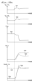
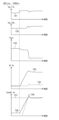
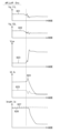
- FIGS. 8, 9, and 10 schematically show waveforms of voltages and currents actually measured in the first, second, and third turn-on evaluation experiments, respectively.
- the time difference dff_Lon was set to "-300 ns". This approximately corresponds to turning on transistor 12L earlier than transistor 11L by 300 ns.
- the time difference dff_Lon was set to "+100 ns”. This approximately corresponds to turning on the transistor 11L earlier than the transistor 12L by 100 ns.
- the time difference dff_Lon was set to "+500 ns". This approximately corresponds to turning on transistor 11L earlier than transistor 12L by 500 ns. Note that "ns” is an abbreviation for nanoseconds.
- waveforms 711, 712, 713, 714, 715, 716, and 717 are respectively the gate voltage Vg_11L, the gate voltage Vg_12L, the output terminal voltage Vsw, the drain current Id, the collector current Ic, and the sum in the first turn-on evaluation experiment.
- Schematic waveforms of current Imath and load current Io are shown.
- waveforms 721, 722, 723, 724, 725, 726, and 727 are respectively the gate voltage Vg_11L, the gate voltage Vg_12L, the output terminal voltage Vsw, the drain current Id, the collector current Ic, and the sum in the second turn-on evaluation experiment.
- Schematic waveforms of current Imath and load current Io are shown.
- waveforms 731, 732, 733, 734, 735, 736, and 737 are respectively the gate voltage Vg_11L, the gate voltage Vg_12L, the output terminal voltage Vsw, the drain current Id, the collector current Ic, and the sum in the third turn-on evaluation experiment.
- Schematic waveforms of current Imath and load current Io are shown.
- 8 to 10 are derived from the current flowing on the board used for evaluation and the inductance component of the pattern on the board (see FIGS. 13 to 16 to be described later). as well).
- the waveforms shown in FIGS. 8 to 10 are schematic representations of the actually measured waveforms, and the noise components contained in the actually measured waveforms are not shown in FIGS. The same is true for ).
- the dashed straight line 718 in FIG. 8, the dashed straight line 728 in FIG. 9, and the dashed straight line 738 in FIG. represents the slope of the sum current Imath at .
- the increase rate of the sum current Imath changes abruptly in the process of increasing the sum current Imath accompanying the turn-on of the switching element 10L.
- the transistor 12L since the transistor 12L is turned on first, the sum current Imath increases only by the increase in the collector current Ic, and then the transistor 11L is turned on, so that the increase rate of the sum current Imath increases. Because it does.
- the transistor 11L since the transistor 11L is turned on first, the sum current Imath increases only by the increase in the drain current Id, and then the transistor 12L is turned on, so that the increase rate of the sum current Imath increases. Because it does.
- the increase rate of the sum current Imath is kept substantially constant in the process of increasing the sum current Imath accompanying the turn-on of the switching element 10L. This means that the drain current Id and the collector current Ic increase at approximately the same rate and at the same time in the process of increasing the sum current Imath.
- the turn-on loss Eon is minimized under the condition that the rate of increase of the sum current Imath is kept substantially constant in the process of increasing the sum current Imath as the switching element 10L is turned on.
- waveform 760 shows the relationship between turn-on loss Eon and time difference dff_Lon in the turn-on evaluation experiment.
- a turn-on loss Eon is a switching loss when the switching element 10L is turned on. That is, the turn-on loss Eon is the loss generated in the switching element 10L when the switching element 10L transitions from the OFF state to the ON state.
- the turn-on loss Eon corresponds to the sum of the turn-on loss of the transistor 11L and the turn-on loss of the transistor 12L.
- the turn-on loss of the transistor 11L is switching loss that occurs in the transistor 11L when the transistor 11L transitions from an off state to an on state.
- the turn-on loss of the transistor 12L is switching loss that occurs in the transistor 12L when the transistor 12L transitions from the off state to the on state.
- waveform 770 shows the relationship between recovery loss Err and time difference dff_Lon in the turn-on evaluation experiment.
- the recovery loss Err is a recovery loss that occurs in the diodes 11Hd and 13H of the high side switching element 10H when the low side switching element 10 is turned on (this recovery loss occurs mainly in the diode 13H).
- 11 and 12 do not show specific numerical values of the turn-on loss Eon and the recovery loss Err, but the recovery loss Err is sufficiently smaller than the turn-on loss Eon (for example, 1/10 to several 10 minutes). ). Therefore, when discussing the total switching loss of the switching elements 10H and 10L, it can be said that attention should be paid only to the turn-on loss Eon.
- the turn-on loss Eon can be minimized by setting the time difference dff_Lon to approximately "+100 ns".
- is considerably large when the switching element 10L is turned on, the current flows only through one of the transistors 11L and 12L for a long period of time, leading to an increase in the turn-on loss Eon.
- the time difference dff_Lon is close to zero, the switching element 10L is turned on in such a manner that the currents are almost evenly distributed to the transistors 11L and 12L, so a reduction in the turn-on loss Eon can be expected.
- the time difference dff_Lon suitable for minimizing the turn-on loss Eon varies depending on the combination of characteristics of the transistors 11L and 12L.
- the semiconductor device 1 has a delay circuit 23L so that an arbitrary time difference dff_Lon can be provided between the turn-on timings of the transistors 11L and 12L.
- the time difference dff_Lon for minimizing the turn-on loss Eon should be determined through experiments or the like in the design stage, manufacturing stage, or shipping process of the semiconductor device 1, and the determined time difference dff_Lon should be adopted in the delay circuit 23L. .
- the delay circuit 23L reduces the switching loss (i.e., It is preferable to set the time difference dff_Lon so that the turn-on loss (Eon) is reduced.
- the delay circuit 23L is arranged so that the timing at which the rate of increase of the drain current Id of the transistor 11L is maximized and the timing at which the rate of increase of the collector current Ic of the transistor 12L is maximized coincide with each other. It is preferable to provide a time difference dff_Lon.
- the turn-on loss was evaluated by focusing on the low-side switching element 10L, and the configuration of the delay circuit 23L based on the evaluation results was described above, but the high-side delay circuit 27H is designed similarly.
- the delay circuit 27H reduces the switching loss at the turn-on of the switching element 10H (hereinafter referred to as It is preferable to set the time difference dff_Hon so that the turn-on loss Eon') is reduced.
- the delay circuit 27H provides a time difference dff_Hon so that the timing at which the rate of increase of the drain current of the transistor 11H is maximized and the timing at which the rate of increase of the collector current of the transistor 12H is maximized. and good.
- a turn-on loss Eon' is a loss generated in the switching element 10H when the switching element 10H transitions from an off state to an on state.
- the turn-on loss Eon' corresponds to the sum of the turn-on loss of transistor 11H and the turn-on loss of transistor 12H.
- the turn-on loss of the transistor 11H is switching loss that occurs in the transistor 11H when the transistor 11H transitions from an off state to an on state.
- the turn-on loss of the transistor 12H is switching loss that occurs in the transistor 12H when the transistor 12H transitions from the off state to the on state.
- FIGS. 13, 14, 15, and 16 schematically show waveforms of voltages and currents actually measured in the first, second, third, and fourth turn-off evaluation experiments, respectively.
- the time difference dff_Loff was set to "-200 ns". This approximately corresponds to turning off the transistor 12L earlier than the transistor 11L by 200 ns.
- the time difference dff_Loff was set to "0 ns”. This approximately corresponds to turning off transistors 11L and 12L at the same time.
- the time difference dff_Loff was set to "+300 ns".
- waveforms 811, 812, 813, 814, 815, 816, and 817 are respectively the gate voltage Vg_11L, the gate voltage Vg_12L, the output terminal voltage Vsw, the drain current Id, the collector current Ic, and the sum in the first turn-off evaluation experiment.
- Schematic waveforms of current Imath and load current Io are shown.
- waveforms 821, 822, 823, 824, 825, 826, and 827 are the gate voltage Vg_11L, the gate voltage Vg_12L, the output terminal voltage Vsw, the drain current Id, the collector current Ic, and the sum, respectively, in the second turn-off evaluation experiment.
- waveforms 831, 832, 833, 834, 835, 836, and 837 are respectively the gate voltage Vg_11L, the gate voltage Vg_12L, the output terminal voltage Vsw, the drain current Id, the collector current Ic, and the sum in the third turn-off evaluation experiment.
- waveforms of current Imath and load current Io are shown. In FIG.
- waveforms 841, 842, 843, 844, 845, 846, and 847 are the gate voltage Vg_11L, the gate voltage Vg_12L, the output terminal voltage Vsw, the drain current Id, the collector current Ic, and the sum, respectively, in the fourth turn-off evaluation experiment. Schematic waveforms of current Imath and load current Io are shown.
- the output terminal voltage Vsw When the switching element 10L is turned off, in the process of the transistor 11L or 12L transitioning from the ON state to the OFF state, the output terminal voltage Vsw once rises from around 0 V, drops, and then rises sharply (waveform 813, 823, 833 and 843).
- the first rise in the output terminal voltage Vsw occurs in the process of turning off the transistor 11L or 12L.
- the second rise in the output terminal voltage Vsw occurs in the process in which one of the transistors 11L and 12L turns off and then the other turns off, or in the process in which the transistors 11L and 12L simultaneously turn off. do.
- the turn-off loss Eoff increases (the turn-off loss Eoff will be described later). Therefore, shortening the length of the period as much as possible or to some extent is suitable for minimizing the turn-off loss Eoff. Also, the ratio of the currents flowing through the transistors 11L and 12L in the process of the switching element 10L transitioning from the ON state to the OFF state also affects the turn-off loss Eoff. Therefore, it is necessary to set the time difference dff_Loff in consideration of these to minimize the turn-off loss Eoff.
- waveform 860 shows the relationship between turn-off loss Eoff and time difference dff_Loff in the turn-off evaluation experiment.
- a turn-off loss Eoff is a switching loss when the switching element 10L is turned off. That is, the turn-off loss Eoff is loss generated in the switching element 10L when the switching element 10L transitions from the ON state to the OFF state.
- the turn-off loss Eoff corresponds to the sum of the turn-off loss of the transistor 11L and the turn-off loss of the transistor 12L.
- the turn-off loss of the transistor 11L is switching loss that occurs in the transistor 11L when the transistor 11L transitions from the ON state to the OFF state.
- the turn-off loss of the transistor 12L is switching loss that occurs in the transistor 12L when the transistor 12L transitions from the ON state to the OFF state.
- the turn-off loss Eoff can be minimized by setting the time difference dff_Loff to approximately "+300 ns".
- the time difference dff_Loff is "+300 ns" (see FIG. 15)
- the drain current Id of the transistor 11L decreases as the transistor 11L turns off first, and the collector current Id of the transistor 12H compensates for the decrease.
- Current Ic increases.
- the collector current Ic increases to some extent (in the process of increasing the collector current Ic)
- the transistor 12L transitions to the off state.
- the time difference dff_Loff suitable for minimizing the turn-off loss Eoff varies depending on the combination of characteristics of the transistors 11L and 12L.
- the semiconductor device 1 has a delay circuit 23L so that an arbitrary time difference dff_Loff can be provided between the turn-off timings of the transistors 11L and 12L.
- dff_Loff it is preferable to determine the time difference dff_Loff for minimizing the turn-off loss Eoff through experiments or the like in the design stage, manufacturing stage, or shipping process of the semiconductor device 1, and to adopt the determined time difference dff_Loff in the delay circuit 23L. .
- the delay circuit 23L reduces the switching loss (i.e., It is preferable to set the time difference dff_Loff so that the turn-off loss (Eoff) is reduced.
- a second predetermined change in the drive control signal LIN (here, When turning off the transistors 11L and 12L in response to the falling edge), the delay circuit 23L increases the collector current Ic of the transistor 12L by turning off the transistor 11L before the transistor 12L. It is preferable to set the time difference dff_Loff so that the transistor 12L is turned off when the ratio of the collector current Ic to the sum (Imath) of the drain current Id and the collector current Ic is equal to or less than a predetermined ratio.
- the predetermined percentage may be selected, for example, within the range of 50% to 95%.
- the turn-off loss was evaluated by focusing on the low-side switching element 10L, and the configuration of the delay circuit 23L based on the evaluation results was described above, but the high-side delay circuit 27H is similarly designed.
- the delay circuit 27H reduces the switching loss at the turn-off of the switching element 10H (hereinafter referred to as It is preferable to set the time difference dff_Hoff so that the turn-off loss Eoff') is reduced.
- delay circuit 27H causes transistor 11H to turn off before transistor 12H, thereby increasing the collector current of transistor 12H and then turning off transistor 11H.
- the time difference dff_Hoff may be set such that the transistor 12H turns off when the ratio of the collector current of the transistor 12H to the sum of the drain current and the collector current of the transistor 12H is less than or equal to a predetermined ratio.
- a turn-off loss Eoff' is a loss generated in the switching element 10H when the switching element 10H transitions from the ON state to the OFF state.
- the turn-off loss Eoff' corresponds to the sum of the turn-off loss of transistor 11H and the turn-off loss of transistor 12H.
- the turn-off loss of the transistor 11H is switching loss that occurs in the transistor 11H when the transistor 11H transitions from the ON state to the OFF state.
- the turn-off loss of the transistor 12H is switching loss that occurs in the transistor 12H when the transistor 12H transitions from the ON state to the OFF state.
- the switching elements 10H and 10L each have first to third elements.
- the first element is a transistor 11H or 11L composed of a MOSFET.
- the second element is a transistor 12H or 12L made up of an IGBT.
- a third element is a diode 13H or 13L connected in parallel to the first and second elements.
- the diode 13H or 13L is a Schottky barrier diode as described above. However, it is also possible to employ a PN junction diode as the diode 13H or 13L.
- the Schottky barrier diode as the diode 13H or 13L, the switching loss (Eon, Eon') at the time of turn-on in each switching element can be kept low, and the steady-state loss in the diode during regeneration can be kept low. can.
- the effect of suppressing these losses becomes remarkable when the transistors 11H and 11L and the diodes 13H and 13L are formed using silicon carbide (SiC).
- a second embodiment of the semiconductor device 1 will be described.
- a plurality of half bridge circuits may be provided by switching elements 10H and 10L.
- drivers 20H and 20L, boot circuit 30, gate resistors 41H, 42H, 41L and 42L, output terminal TM11, low side terminal TM13, boot terminal TM15, and control input terminal are provided for each half bridge circuit.
- TM16 and TM17 and capacitor CB may be provided.
- the gate resistance can be omitted (hereafter, the existence of the gate resistance is ignored).
- the semiconductor device 1 may be provided with a U-phase unit circuit, a V-phase unit circuit, and a W-phase unit circuit.
- Each unit circuit includes a half bridge circuit with switching elements 10H and 10L, drivers 20H and 20L, and a boot circuit 30.
- FIG. An output terminal TM11, a low-side terminal TM13, a boot terminal TM15, control input terminals TM16 and TM17, and a capacitor CB are provided for each unit circuit.
- the load LD in this case may be a three-phase motor having a U-phase coil, a V-phase coil and a W-phase coil.
- U-phase coil, the V-phase coil, and the W-phase coil are star-connected (Y-connected), one end of the U-phase coil, one end of the V-phase coil, and one end of the W-phase coil are connected to the output terminals for the U-phase, respectively.
- TM11, V-phase output terminal TM11, and W-phase output terminal TM11 are connected, and the other end of the U-phase coil, the other end of the V-phase coil, and the other end of the W-phase coil are connected in common.
- a high side driver 20H which is a driver circuit for the switching element 10H
- a low side driver 20L which is a driver circuit for the switching element 10L
- a control signal generation circuit in the high side driver 20H generates a control signal CNT_11H for controlling the state of the transistor 11H and a control signal CNT_12H for controlling the state of the transistor 12H based on the drive control signal HIN.
- the high side driver 20H drives the gate of the transistor 11H based on the control signal CNT_11H, and drives the gate of the transistor 12H based on the control signal CNT_12H.
- a control signal generation circuit for the high side driver 20H is formed at each portion referenced by reference numerals 21H to 27H.
- a control signal generation circuit in the low-side driver 20L generates a control signal CNT_11L for controlling the state of the transistor 11L and a control signal CNT_12L for controlling the state of the transistor 12L based on the drive control signal LIN.
- the low-side driver 20L drives the gate of the transistor 11L based on the control signal CNT_11L, and drives the gate of the transistor 12L based on the control signal CNT_12L.
- a control signal generation circuit for the low side driver 20L is formed at each portion referenced by reference numerals 21L to 23L.
- the switching elements (10H, 10L) are turned on in response to the down edge of the drive control signals (HIN, LIN), and the switching elements (10H, 10H) are turned on in response to the up edge of the drive control signals (HIN, LIN).
- , 10L) may be turned off.
- FET field effect transistor
- a semiconductor device (1) is a parallel connection circuit of a first transistor (for example, 11L) formed of a field effect transistor and a second transistor (for example, 12L) formed of an insulated gate bipolar transistor. and a driver circuit (e.g. 20L) configured to drive the switching element in response to an input control signal (e.g. LIN), wherein the driver circuit drives the switching element When transitioning from the first state to the second state, the transition timing of the first transistor from the first state to the second state and the transition timing of the second transistor from the first state to the second state and , and one of the first state and the second state is in the OFF state and the other is in the ON state (first configuration).
- a driver circuit e.g. 20L
- the driver circuit controls the state of the second transistor and a first control signal (for example, CNT_11L) for controlling the state of the first transistor based on the input control signal.
- a control signal generation circuit eg, 21L-23L
- the control signal generation circuit generates a change timing (for example, t_L1 or t_L3) of the first control signal based on a change of the input control signal and the input control signal.
- the delay circuit turns on the first transistor and the second transistor in response to a predetermined change (for example, a change from low level to high level) in the input control signal.
- a predetermined change for example, a change from low level to high level
- a first timing for example, t_L1
- a timing for turning on the second transistor based on the predetermined change for example, a timing for turning on the second transistor based on the predetermined change.
- a configuration (third configuration) that provides a difference from the second timing (for example, t_L2) at which the level change is caused in the second control signal may be employed.
- the delay circuit reduces switching loss (e.g., Eon) at turn-on of the switching element compared to when the first timing and the second timing are simultaneous.
- the configuration (fourth configuration) may be such that the difference is provided.
- the delay circuit determines the timing at which the rate of increase of the drain current of the first transistor becomes maximum and the A configuration (fifth configuration) in which the difference is provided so as to coincide with the timing at which the rate of increase of the collector current of the second transistor is maximized may be employed.
- the delay circuit turns off the first transistor and the second transistor in response to a predetermined change (for example, a change from high level to low level) in the input control signal.
- a predetermined change for example, a change from high level to low level
- a first timing for example, t_L3
- a timing for turning off the second transistor based on the predetermined change for example, a predetermined change from the input control signal.
- a configuration (sixth configuration) that provides a difference from the second timing (for example, t_L4) at which the level change is caused in the second control signal may be employed.
- the delay circuit has a reduced switching loss (e.g., Eoff) at turn-off of the switching element compared to when the first timing and the second timing are simultaneous.
- Eoff switching loss
- the delay circuit causes the first transistor to turn off before the second transistor. and then divide the difference such that the second transistor turns off when the ratio of the collector current to the sum of the drain current and the collector current is less than or equal to a predetermined ratio.
- a configuration (eighth configuration) may be employed.
- a plurality of sets of the switching element and the driver circuit are provided, and two switching elements in two sets are connected in series to form a half bridge circuit.
- the configuration (the ninth configuration) may be used.
- each set may have a configuration (tenth configuration) in which Schottky barrier diodes (13H, 13L) are connected in parallel to the second transistor.
- the first transistor and the Schottky barrier diode may be formed using silicon carbide (eleventh configuration).
- the semiconductor device may have a configuration in which a plurality of the herb bridge circuits are provided (a twelfth configuration).
- SYS system (load drive system) 1 semiconductor device 2 MPU 3 voltage source CB capacitor LD load Rs sense resistor 10H high side switching element 10L low side switching element 11H, 11L transistor (MOSFET) 12H, 12L Transistor (IGBT) 13H, 13L diodes (Schottky barrier diodes) 11Hd, 11Ld diode (parasitic diode) 20H high side driver 20L low side driver 30 boot circuit 31 diode 41H, 42H, 41L, 42L gate resistor 21H input circuit 22H level shifter 23H pulse generation circuit 24H level shifter 25H filter 26H latch circuit 27H delay circuit 28H, 29H output circuit 21L input circuit 22L Control logic circuit 23L Delay circuit 24L Level shifter 25L, 26L Output circuit
Abstract
This semiconductor device is provided with: a switching element having a circuit in which a first transistor formed of a field effect transistor and a second transistor formed of an insulated gate bipolar transistor are connected in parallel; and a driver circuit configured to drive the switching element in response to an input control signal. When causing the switching element to make a transition from a first state to a second state, the driver circuit makes a difference between: a transition timing from the first state to the second state of the first transistor; and a transition timing from the first state to the second state of the second transistor. One of the first state and the second state is an off-state, and the other is an on-state.
Description
本開示は、半導体装置に関する。
The present disclosure relates to semiconductor devices.
スイッチング素子を用いて負荷(コイル等)を駆動する装置がある。
There are devices that drive loads (coils, etc.) using switching elements.
複数のトランジスタの並列接続回路にてスイッチング素子を構成する場合がある。この種のスイッチング素子において、スイッチング損失の低減に関して改善の余地がある。
A switching element may be composed of a parallel connection circuit of a plurality of transistors. In this type of switching element, there is room for improvement in terms of reducing switching loss.
本開示はスイッチング損失の低減に寄与する半導体装置を提供することを目的とする。
An object of the present disclosure is to provide a semiconductor device that contributes to reducing switching loss.
本開示に係る半導体装置は、電界効果トランジスタにて構成された第1トランジスタ及び絶縁ゲートバイポーラトランジスタにて構成された第2トランジスタの並列接続回路を有するスイッチング素子と、入力制御信号に応じて前記スイッチング素子を駆動するよう構成されたドライバ回路と、を備え、前記ドライバ回路は、前記スイッチング素子を第1状態から第2状態に遷移させる際、前記第1トランジスタの前記第1状態から前記第2状態への遷移タイミングと、前記第2トランジスタの前記第1状態から前記第2状態への遷移タイミングと、を異ならせ、前記第1状態及び前記第2状態の内、一方はオフ状態であって且つ他方はオン状態である。
A semiconductor device according to the present disclosure includes a switching element having a parallel connection circuit of a first transistor configured by a field effect transistor and a second transistor configured by an insulated gate bipolar transistor, and the switching element according to an input control signal. a driver circuit configured to drive a device, the driver circuit configured to drive the first transistor from the first state to the second state when transitioning the switching device from the first state to the second state. and the transition timing of the second transistor from the first state to the second state are different, and one of the first state and the second state is an off state, and The other is on.
本開示によれば、スイッチング損失の低減に寄与する半導体装置を提供することが可能となる。
According to the present disclosure, it is possible to provide a semiconductor device that contributes to reducing switching loss.
以下、本開示の実施形態の例を、図面を参照して具体的に説明する。参照される各図において、同一の部分には同一の符号を付し、同一の部分に関する重複する説明を原則として省略する。尚、本明細書では、記述の簡略化上、情報、信号、物理量、素子又は部位等を参照する記号又は符号を記すことによって、該記号又は符号に対応する情報、信号、物理量、素子又は部位等の名称を省略又は略記することがある。例えば、後述の“10H”によって参照されるハイサイドスイッチング素子10Hは(図1参照)、ハイサイドスイッチング素子10Hと表記されることもあるし、スイッチング素子10Hと略記されることもあり得るが、それらは全て同じものを指す。
Hereinafter, examples of embodiments of the present disclosure will be specifically described with reference to the drawings. In each figure referred to, the same parts are denoted by the same reference numerals, and redundant descriptions of the same parts are omitted in principle. In this specification, for simplification of description, by describing symbols or codes that refer to information, signals, physical quantities, elements or parts, etc., information, signals, physical quantities, elements or parts corresponding to the symbols or codes are used. etc. may be omitted or abbreviated. For example, a high-side switching element 10H (see FIG. 1) referred to by "10H" described later may be referred to as the high-side switching element 10H or may be abbreviated as the switching element 10H. they all refer to the same thing.
まず、本開示の実施形態の記述にて用いられる幾つかの用語について説明を設ける。グランドとは、基準となる0V(ゼロボルト)の電位を有する基準導電部を指す又は0Vの電位そのものを指す。基準導電部は金属等の導体にて形成される。0Vの電位をグランド電位と称することもある。本開示の実施形態において、特に基準を設けずに示される電圧はグランドから見た電位を表す。
First, some terms used in the description of the embodiments of the present disclosure will be explained. The ground refers to a reference conductive portion having a potential of 0 V (zero volt) as a reference, or refers to a potential of 0 V itself. The reference conductive portion is made of a conductor such as metal. A potential of 0 V is sometimes referred to as a ground potential. In embodiments of the present disclosure, voltages shown without specific reference represent potentials with respect to ground.
レベルとは電位のレベルを指し、任意の注目した信号又は電圧についてハイレベルはローレベルよりも高い電位を有する。任意の注目した信号又は電圧について、信号又は電圧がハイレベルにあるとは厳密には信号又は電圧のレベルがハイレベルにあることを意味し、信号又は電圧がローレベルにあるとは厳密には信号又は電圧のレベルがローレベルにあることを意味する。信号についてのレベルは信号レベルと表現されることがあり、電圧についてのレベルは電圧レベルと表現されることがある。
A level refers to a level of potential, and for any signal or voltage of interest, a high level has a higher potential than a low level. For any signal or voltage of interest, strictly speaking that the signal or voltage is at a high level means that the signal or voltage is at a high level, and strictly speaking that the signal or voltage is at a low level. It means that the signal or voltage level is at low level. Levels for signals are sometimes referred to as signal levels, and levels for voltages are sometimes referred to as voltage levels.
任意の注目した信号又は電圧において、ローレベルからハイレベルへの切り替わりをアップエッジ(或いはライジングエッジ)と称し、ローレベルからハイレベルへの切り替わりのタイミングをアップエッジタイミング(或いはライジングエッジタイミング)と称する。同様に、任意の注目した信号又は電圧において、ハイレベルからローレベルへの切り替わりをダウンエッジ(或いはフォーリングエッジ)と称し、ハイレベルからローレベルへの切り替わりのタイミングをダウンエッジタイミング(或いはフォーリングエッジタイミング)と称する。
In any signal or voltage of interest, the switching from low level to high level is called up edge (or rising edge), and the timing of switching from low level to high level is called up edge timing (or rising edge timing). . Similarly, for any signal or voltage of interest, the switching from high level to low level is called the falling edge (or falling edge), and the timing of switching from high level to low level is called the falling edge timing (or falling edge). edge timing).
ハイレベル又はローレベルの信号レベルをとる任意の信号について、当該信号のレベルがハイレベルとなる期間をハイレベル期間と称し、当該信号のレベルがローレベルとなる期間をローレベル期間と称する。ハイレベル又はローレベルの電圧レベルをとる任意の電圧についても同様である。
For any signal that takes a signal level of high level or low level, a period during which the level of the signal is high is called a high level period, and a period during which the level of the signal is low is called a low level period. The same is true for any voltage that takes a high or low voltage level.
MOSFETを含むFET(電界効果トランジスタ)として構成された任意のトランジスタについて、オン状態とは、当該トランジスタのドレイン及びソース間が導通している状態を指し、オフ状態とは、当該トランジスタのドレイン及びソース間が非導通となっている状態(遮断状態)を指す。MOSFETは、特に記述無き限り、エンハンスメント型のMOSFETであると解される。MOSFETは金属酸化膜半導体電界効果トランジスタ(Metal-Oxide-Semiconductor Field-Effect Transistor)の略称である。また、特に記述なき限り、任意のMOSFETにおいて、バックゲートはソースに短絡されていると解される。
For any transistor configured as a FET (Field Effect Transistor), including a MOSFET, the ON state refers to the state in which there is conduction between the drain and source of the transistor, and the OFF state refers to the state in which there is conduction between the drain and source of the transistor. It refers to the state in which the current between the two is non-conducting (blocking state). MOSFETs are understood to be enhancement mode MOSFETs unless otherwise stated. MOSFET is an abbreviation for Metal-Oxide-Semiconductor Field-Effect Transistor. Also, unless otherwise stated, in any MOSFET, the back gate is understood to be shorted to the source.
MOSFETの電気的特性にはゲート閾電圧が含まれる。Nチャネル型のMOSFETについて、当該MOSFETのゲート電位が当該MOSFETのソース電位よりも高く、且つ、当該MOSFETのゲート-ソース間電圧の大きさが当該MOSFETのゲート閾電圧以上であるとき、当該MOSFETはオン状態となり、そうでないとき、当該MOSFETはオフ状態となる。任意のMOSFETにおいて、ゲート-ソース間電圧とは、ソースの電位から見たゲートの電位を指す。
The electrical characteristics of a MOSFET include the gate threshold voltage. For an N-channel MOSFET, when the gate potential of the MOSFET is higher than the source potential of the MOSFET and the magnitude of the gate-source voltage of the MOSFET is equal to or greater than the gate threshold voltage of the MOSFET, the MOSFET is It will be on, otherwise the MOSFET will be off. In any MOSFET, the gate-to-source voltage refers to the potential of the gate relative to the potential of the source.
IGBTとして構成された任意のトランジスタについて、オン状態とは、当該トランジスタのコレクタ及びエミッタ間が導通している状態を指し、オフ状態とは、当該トランジスタのコレクタ及びエミッタ間が非導通となっている状態(遮断状態)を指す。IGBTは絶縁ゲートバイポーラトランジスタ(Insulated Gate Bipolar Transistor)の略称である。
For any transistor configured as an IGBT, the on state refers to conduction between the transistor's collector and emitter, and the off state refers to non-conduction between the transistor's collector and emitter. It refers to the state (blocked state). IGBT is an abbreviation for Insulated Gate Bipolar Transistor.
IGBTの電気的特性にはゲート閾電圧が含まれる。Nチャネル型のIGBTについて、当該IGBTのゲート電位が当該IGBTのエミッタ電位よりも高く、且つ、当該IGBTのゲート-エミッタ間電圧の大きさが当該IGBTのゲート閾電圧以上であるとき、当該IGBTはオン状態となり、そうでないとき、当該IGBTはオフ状態となる。任意のIGBTにおいて、ゲート-エミッタ間電圧とは、エミッタの電位から見たゲートの電位を指す。
The electrical characteristics of IGBTs include the gate threshold voltage. For an N-channel IGBT, when the gate potential of the IGBT is higher than the emitter potential of the IGBT and the gate-emitter voltage of the IGBT is equal to or higher than the gate threshold voltage of the IGBT, the IGBT The IGBT is turned on, otherwise the IGBT is turned off. In any IGBT, the gate-emitter voltage refers to the potential of the gate as seen from the potential of the emitter.
任意の回路素子、配線、ノードなど、回路を形成する複数の部位間についての接続とは、特に記述なき限り、電気的な接続を指すと解して良い。
Connections between multiple parts forming a circuit, such as arbitrary circuit elements, wirings, and nodes, may be understood to refer to electrical connections unless otherwise specified.
図1に第1実施形態に係るシステムSYSの全体構成を示す。システムSYSを負荷駆動システムと称することができる。システムSYSは、負荷LDを駆動するための半導体装置1と、MPU(Micro Processing Unit)2と、電圧源3を備えると共に、コンデンサCBと、センス抵抗Rsと、を備える。半導体装置1を、負荷駆動装置又は負荷駆動用半導体装置と称することもできる。
FIG. 1 shows the overall configuration of the system SYS according to the first embodiment. System SYS can be referred to as a load driving system. The system SYS includes a semiconductor device 1 for driving a load LD, an MPU (Micro Processing Unit) 2, a voltage source 3, a capacitor CB, and a sense resistor Rs. The semiconductor device 1 can also be called a load driving device or a load driving semiconductor device.
図2は半導体装置1の外観斜視図である。半導体装置1は、半導体基板上に形成された半導体集積回路を有する半導体チップと、半導体ディスクリート部品と、半導体チップ及び半導体ディスクリート部品を収容する筐体(パッケージ)と、筐体から半導体装置1の外部に対して露出する複数の外部端子と、を備えた電子部品である。半導体チップ及び半導体ディスクリート部品を樹脂にて構成された筐体(パッケージ)内に封入することで半導体装置1が形成される。この種の半導体装置1はIPM(Intelligent Power Modules)と称され得る。尚、図2に示される半導体装置1の外部端子の数及び半導体装置1の筐体の種類は例示に過ぎず、それらを任意に設計可能である。
2 is an external perspective view of the semiconductor device 1. FIG. The semiconductor device 1 includes a semiconductor chip having a semiconductor integrated circuit formed on a semiconductor substrate, a semiconductor discrete component, a housing (package) for housing the semiconductor chip and the semiconductor discrete component, and an exterior of the semiconductor device 1 from the housing. and a plurality of external terminals exposed to the electronic component. A semiconductor device 1 is formed by enclosing a semiconductor chip and semiconductor discrete components in a housing (package) made of resin. This type of semiconductor device 1 can be called IPM (Intelligent Power Modules). The number of external terminals of the semiconductor device 1 and the type of housing of the semiconductor device 1 shown in FIG. 2 are merely examples, and they can be designed arbitrarily.
半導体装置1に設けられる外部端子の一部として、図1には端子TM11~TM17が示されている。端子TM11は出力端電圧Vswが加わる出力端子である。端子TM12はパワー電源電圧VPが加わるパワー電源端子である。端子TM13はローサイド端子である。端子TM14はグランドに接続されるグランド端子である。端子TM15はブート電圧VBが加わるブート端子である。端子TM16は駆動制御信号HINが加わる制御入力端子である。端子TM17は駆動制御信号LINが加わる制御入力端子である。駆動制御信号HIN及びLINは半導体装置1に対する入力制御信号である。
As part of the external terminals provided in the semiconductor device 1, terminals TM11 to TM17 are shown in FIG. A terminal TM11 is an output terminal to which an output terminal voltage Vsw is applied. A terminal TM12 is a power supply terminal to which a power supply voltage VP is applied. Terminal TM13 is a low-side terminal. A terminal TM14 is a ground terminal connected to the ground. A terminal TM15 is a boot terminal to which a boot voltage VB is applied. A terminal TM16 is a control input terminal to which a drive control signal HIN is applied. A terminal TM17 is a control input terminal to which a drive control signal LIN is applied. Drive control signals HIN and LIN are input control signals for the semiconductor device 1 .
まず半導体装置1の外部構成について説明する。負荷LDは出力端子TM11に接続され、出力端子TM11を通じて供給される電力に基づいて駆動する。負荷LDは誘導性負荷を含む。ここでは、負荷LDとしてのコイルの一端は出力端子TM11に接続され、且つ、負荷LDとしてのコイルの他端はパワー電源電圧VPが加わる配線に接続されるものとする。負荷LDはモータのコイル(電機子巻線)であって良い。但し、負荷LDは誘導性負荷を含むものであれば任意である。出力端子TM11及び負荷LD間に流れる電流を、以下、負荷電流と称し、負荷電流を記号“Io”にて参照する。
First, the external configuration of the semiconductor device 1 will be described. The load LD is connected to the output terminal TM11 and driven based on power supplied through the output terminal TM11. Load LD includes an inductive load. Here, one end of the coil as the load LD is connected to the output terminal TM11, and the other end of the coil as the load LD is connected to the wiring to which the power supply voltage VP is applied. The load LD may be a motor coil (armature winding). However, the load LD is arbitrary as long as it includes an inductive load. A current flowing between the output terminal TM11 and the load LD is hereinafter referred to as a load current, and the load current is referred to by the symbol "Io".
コンデンサCBは半導体装置1の外部に設けられたブートストラップコンデンサである。半導体装置1の外部において、コンデンサCBは端子TM11及びTM15間に設けられる。即ち、コンデンサCBの一端は出力端子TM11に接続され、コンデンサCBの他端はブート端子TM15に接続される。尚、コンデンサCBを半導体装置1に内蔵する変形も可能である。
A capacitor CB is a bootstrap capacitor provided outside the semiconductor device 1 . Outside the semiconductor device 1, the capacitor CB is provided between the terminals TM11 and TM15. That is, one end of the capacitor CB is connected to the output terminal TM11, and the other end of the capacitor CB is connected to the boot terminal TM15. A modification in which the capacitor CB is incorporated in the semiconductor device 1 is also possible.
電圧源3は所定の正の直流電圧値を有する電源電圧VPを出力する。電源電圧VPをパワー電源電圧と称することもある。パワー電源電圧VPはパワー電源端子TM12に入力される。電源電圧VPの電圧値は任意である。例えば、電源電圧VPは数100V(ボルト)である。
The voltage source 3 outputs a power supply voltage VP having a predetermined positive DC voltage value. The power supply voltage VP may also be called a power supply voltage. A power supply voltage VP is input to a power supply terminal TM12. The voltage value of the power supply voltage VP is arbitrary. For example, the power supply voltage VP is several hundred V (volts).
ローサイド端子TM13はセンス抵抗Rsを介してグランドに接続される。センス抵抗Rsを半導体装置1に内蔵する変形も可能である。尚、ローサイド端子TM13はグランドに対して直接接続される場合もある。半導体装置1では、センス抵抗Rsの電圧降下に基づき後述のスイッチング素子10H又は10Lに対する過電流保護動作を行うことができる。但し、システムSYSにおいてセンス抵抗Rsを省略することも可能である(センス抵抗Rsの抵抗値が0Ωであると解しても良い)。
The low-side terminal TM13 is connected to the ground via the sense resistor Rs. A modification in which the sense resistor Rs is built in the semiconductor device 1 is also possible. Incidentally, the low-side terminal TM13 may be directly connected to the ground. In the semiconductor device 1, an overcurrent protection operation for a switching element 10H or 10L, which will be described later, can be performed based on the voltage drop of the sense resistor Rs. However, it is also possible to omit the sense resistor Rs in the system SYS (it may be understood that the resistance value of the sense resistor Rs is 0Ω).
MPU2は駆動制御信号HIN及びLINを生成及び出力する。駆動制御信号HINは制御入力端子TM16に入力され、駆動制御信号LINは制御入力端子TM17に入力される。駆動制御信号HIN及びLINは夫々に、ハイレベル又はローレベルの何れかをとるデジタル信号(二値化信号)である。駆動制御信号HIN及びLINにおけるハイレベルはMPU2の電源電圧VCC2のレベルと一致し、駆動制御信号HIN及びLINにおけるローレベルはグランドのレベルと一致する(図3参照)。ここにおける一致は実質的に一致することをも含む概念である。電源電圧VCC2の電圧値は任意である。例えば、電源電圧VCC2は5V(ボルト)である。
The MPU 2 generates and outputs drive control signals HIN and LIN. The drive control signal HIN is input to the control input terminal TM16, and the drive control signal LIN is input to the control input terminal TM17. Each of the drive control signals HIN and LIN is a digital signal (binary signal) that takes either a high level or a low level. High levels of the drive control signals HIN and LIN match the level of the power supply voltage VCC2 of the MPU 2, and low levels of the drive control signals HIN and LIN match the ground level (see FIG. 3). Matching here is a concept that also includes substantially matching. The voltage value of power supply voltage VCC2 is arbitrary. For example, the power supply voltage VCC2 is 5V (volt).
次に、半導体装置1の内部構成を説明する。図1に示す如く、半導体装置1は、ハイサイドスイッチング素子10H及びローサイドスイッチング素子10Lと、ハイサイドドライバ20H及びローサイドドライバ20Lと、ブート用回路30と、ゲート抵抗41H、42H、41L及び42Lと、を備える。
Next, the internal configuration of the semiconductor device 1 will be described. As shown in FIG. 1, the semiconductor device 1 includes a high-side switching element 10H and a low-side switching element 10L, a high-side driver 20H and a low-side driver 20L, a boot circuit 30, gate resistors 41H, 42H, 41L and 42L, Prepare.
スイッチング素子10H及び10Lは、夫々に、電界効果トランジスタと絶縁ゲートバイポーラトランジスタの並列接続回路を有する複合スイッチング素子である。
The switching elements 10H and 10L are composite switching elements each having a parallel connection circuit of a field effect transistor and an insulated gate bipolar transistor.
より具体的には、スイッチング素子10Hは、Nチャネル型のMOSFETであるトランジスタ11Hと、Nチャネル型のIGBTであるトランジスタ12Hと、ショットキバリアダイオードであるダイオード13Hと、を備える。トランジスタ11H及び12H並びにダイオード13Hを半導体ディスクリート部品にて形成することができる。ダイオード11Hdは、トランジスタ11Hに付加された寄生ダイオードを表す。スイッチング素子10Hは、端子15H及び16Hを有する。トランジスタ11Hのドレイン、トランジスタ12Hのコレクタ及びダイオード13Hのカソードは、端子15Hに共通接続される。トランジスタ11Hのソース、トランジスタ12Hのエミッタ及びダイオード13Hのアノードは、端子16Hに共通接続される。寄生ダイオード11Hdのアノード、カソードは、夫々、トランジスタ11Hのソース、ドレインに接続される。
More specifically, the switching element 10H includes a transistor 11H that is an N-channel MOSFET, a transistor 12H that is an N-channel IGBT, and a diode 13H that is a Schottky barrier diode. Transistors 11H and 12H and diode 13H can be formed of semiconductor discrete components. Diode 11Hd represents a parasitic diode added to transistor 11H. The switching element 10H has terminals 15H and 16H. The drain of transistor 11H, the collector of transistor 12H and the cathode of diode 13H are commonly connected to terminal 15H. The source of transistor 11H, the emitter of transistor 12H and the anode of diode 13H are commonly connected to terminal 16H. The anode and cathode of the parasitic diode 11Hd are connected to the source and drain of the transistor 11H, respectively.
スイッチング素子10Lは、Nチャネル型のMOSFETであるトランジスタ11Lと、Nチャネル型のIGBTであるトランジスタ12Lと、ショットキバリアダイオードであるダイオード13Lと、を備える。トランジスタ11L及び12L並びにダイオード13Lを半導体ディスクリート部品にて形成することができる。ダイオード11Ldは、トランジスタ11Lに付加された寄生ダイオードを表す。スイッチング素子10Lは、端子15L及び16Lを有する。トランジスタ11Lのドレイン、トランジスタ12Lのコレクタ及びダイオード13Lのカソードは、端子15Lに共通接続される。トランジスタ11Lのソース、トランジスタ12Lのエミッタ及びダイオード13Lのアノードは、端子16Lに共通接続される。寄生ダイオード11Ldのアノード、カソードは、夫々、トランジスタ11Lのソース、ドレインに接続される。
The switching element 10L includes a transistor 11L that is an N-channel MOSFET, a transistor 12L that is an N-channel IGBT, and a diode 13L that is a Schottky barrier diode. Transistors 11L and 12L and diode 13L can be formed of semiconductor discrete components. Diode 11Ld represents a parasitic diode added to transistor 11L. The switching element 10L has terminals 15L and 16L. The drain of transistor 11L, the collector of transistor 12L and the cathode of diode 13L are commonly connected to terminal 15L. The source of transistor 11L, the emitter of transistor 12L and the anode of diode 13L are commonly connected to terminal 16L. The anode and cathode of the parasitic diode 11Ld are connected to the source and drain of the transistor 11L, respectively.
端子15Hはパワー電源端子TM12に接続されてパワー電源電圧VPの供給を受ける。端子16Lはローサイド端子TM13に接続される。端子16H及び15Lは半導体装置1内で互いに接続される。端子16H及び15Lは出力端子TM11に接続される。このように、スイッチング素子10H及び10Lは互いに直列接続されることでハーフブリッジ回路を形成する。
The terminal 15H is connected to the power supply terminal TM12 to receive the power supply voltage VP. The terminal 16L is connected to the low side terminal TM13. Terminals 16H and 15L are connected to each other within semiconductor device 1 . Terminals 16H and 15L are connected to output terminal TM11. Thus, the switching elements 10H and 10L are connected in series to form a half bridge circuit.
スイッチング素子10Hは、ハイサイドドライバ20Hの制御の下、端子15H及び16H間を導通させる又は非導通とする。端子15H及び16H間が導通している状態をスイッチング素子10Hのオン状態と称し、端子15H及び16H間が非導通となる状態をスイッチング素子10Hのオフ状態と称する。トランジスタ11H及び12Hの双方がオン状態であるとき、スイッチング素子10Hはオン状態である。トランジスタ11H及び12Hの内、何れか一方がオン状態であって且つ他方がオフ状態であるときにも、スイッチング素子10Hはオン状態である。トランジスタ11H及び12Hの双方がオフ状態であるとき、スイッチング素子10Hはオフ状態である。
The switching element 10H makes the terminals 15H and 16H conductive or non-conductive under the control of the high side driver 20H. A state in which the terminals 15H and 16H are conductive is referred to as an ON state of the switching element 10H, and a state in which the terminals 15H and 16H are non-conductive is referred to as an OFF state of the switching element 10H. When both transistors 11H and 12H are on, switching element 10H is on. The switching element 10H is also on when one of the transistors 11H and 12H is on and the other is off. When both transistors 11H and 12H are off, switching element 10H is off.
スイッチング素子10Lは、ローサイドドライバ20Lの制御の下、端子15L及び16L間を導通させる又は非導通とする。端子15L及び16L間が導通している状態をスイッチング素子10Lのオン状態と称し、端子15L及び16L間が非導通となる状態をスイッチング素子10Lのオフ状態と称する。トランジスタ11L及び12Lの双方がオン状態であるとき、スイッチング素子10Lはオン状態である。トランジスタ11L及び12Lの内、何れか一方がオン状態であって且つ他方がオフ状態であるときにも、スイッチング素子10Lはオン状態である。トランジスタ11L及び12Lの双方がオフ状態であるとき、スイッチング素子10Lはオフ状態である。
The switching element 10L makes the terminals 15L and 16L conductive or non-conductive under the control of the low-side driver 20L. A state in which the terminals 15L and 16L are electrically connected is referred to as an ON state of the switching element 10L, and a state in which the terminals 15L and 16L are not electrically connected is referred to as an OFF state of the switching element 10L. When both transistors 11L and 12L are on, the switching element 10L is on. The switching element 10L is also in the ON state when one of the transistors 11L and 12L is in the ON state and the other is in the OFF state. When both transistors 11L and 12L are off, switching element 10L is off.
トランジスタ11H及び11Lは炭化ケイ素(SiC)を用いて形成される。但し、炭化ケイ素以外の半導体材料(例えばケイ素)を用いてトランジスタ11H及び11Lを形成することも可能である。トランジスタ12H及び12Lはケイ素(Si)を用いて形成されて良い。ダイオード13H及び13Lは炭化ケイ素(SiC)を用いて形成される。但し、炭化ケイ素以外の半導体材料(例えばケイ素)を用いてダイオード13H及び13Lを形成することも可能である。
The transistors 11H and 11L are formed using silicon carbide (SiC). However, it is also possible to form transistors 11H and 11L using a semiconductor material other than silicon carbide (eg, silicon). Transistors 12H and 12L may be formed using silicon (Si). Diodes 13H and 13L are formed using silicon carbide (SiC). However, it is also possible to form the diodes 13H and 13L using a semiconductor material other than silicon carbide (eg, silicon).
以下、任意のトランジスタ又はスイッチング素子について、オン状態、オフ状態を、単に、オン、オフと表現することがある。また、任意のトランジスタ又はスイッチング素子について、オフ状態からオン状態への切り替わりをターンオンと表現し、オン状態からオフ状態への切り替わりをターンオフと表現する。ターンオンが発生するタイミング、ターンオフが発生するタイミングを、夫々、ターンオンタイミング、ターンオフタイミングと表現する。また、任意のトランジスタ又はスイッチング素子について、トランジスタ又はスイッチング素子がオン状態となっている期間をオン期間と称することがあり、トランジスタ又はスイッチング素子がオフ状態となっている期間をオフ期間と称することがある。
Hereinafter, the on state and off state of any transistor or switching element may be simply expressed as on and off. For any transistor or switching element, switching from an off state to an on state is expressed as turn-on, and switching from an on state to an off state is expressed as turn-off. The timing at which turn-on occurs and the timing at which turn-off occurs are expressed as turn-on timing and turn-off timing, respectively. Further, for any transistor or switching element, the period during which the transistor or switching element is on may be referred to as an on period, and the period during which the transistor or switching element is off may be referred to as an off period. be.
ハイサイドドライバ20Hに対し、制御入力端子TM16にて受けた駆動制御信号HINが入力される。また、ハイサイドドライバ20Hはグランドに接続され、且つ、制御電源電圧VCC、出力端電圧Vsw及びブート電圧VBがハイサイドドライバ20Hに入力される。ハイサイドドライバ20Hは、駆動制御信号HINに応じてトランジスタ11H及び12Hの各ゲート電位を制御することでスイッチング素子10Hを駆動する(スイッチング素子10Hの状態を制御する)。制御電源電圧VCCは外部電源(不図示)から半導体装置1に供給される正の直流電圧(例えば15V)である。或いは、半導体装置1にて制御電源電圧VCCが生成されても良い。
The drive control signal HIN received at the control input terminal TM16 is input to the high side driver 20H. Also, the high side driver 20H is connected to the ground, and the control power supply voltage VCC, the output terminal voltage Vsw and the boot voltage VB are input to the high side driver 20H. The high-side driver 20H drives the switching element 10H (controls the state of the switching element 10H) by controlling the gate potentials of the transistors 11H and 12H according to the drive control signal HIN. The control power supply voltage VCC is a positive DC voltage (eg, 15V) supplied to the semiconductor device 1 from an external power supply (not shown). Alternatively, the semiconductor device 1 may generate the control power supply voltage VCC.
ローサイドドライバ20Lに対し、制御入力端子TM17にて受けた駆動制御信号LINが入力される。また、ローサイドドライバ20Lはグランドに接続され、且つ、制御電源電圧VCCがローサイドドライバ20Lに入力される。ローサイドドライバ20Lは、駆動制御信号LINに応じてトランジスタ11L及び12Lの各ゲート電位を制御することでスイッチング素子10Lを駆動する(スイッチング素子10Lの状態を制御する)。
The drive control signal LIN received at the control input terminal TM17 is input to the low-side driver 20L. Also, the low side driver 20L is connected to the ground, and the control power supply voltage VCC is input to the low side driver 20L. The low-side driver 20L drives the switching element 10L (controls the state of the switching element 10L) by controlling the gate potentials of the transistors 11L and 12L according to the drive control signal LIN.
システムSYSにおいて、スイッチング素子10H及び10Lは交互にオンとされ、スイッチング素子10H及び10Lが同時にオンとなることは無い。ブート用回路30とコンデンサCBとで構成されるブートストラップ回路によりブート端子TM15にブート電圧VBが発生する。
In the system SYS, the switching elements 10H and 10L are alternately turned on, and the switching elements 10H and 10L are never turned on at the same time. A boot voltage VB is generated at the boot terminal TM15 by a bootstrap circuit composed of the circuit 30 for booting and the capacitor CB.
ブート用回路30には、制御電源電圧VCCを受けるアノード及びブート端子TM15に接続されたカソードを有するダイオード31が設けられる。スイッチング素子10Hがオフ且つスイッチング素子10Lがオンの期間においてダイオード31を通じてコンデンサCBへ充電電流が供給され、それ以外の期間においてダイオード31を通じたコンデンサCBの放電は発生しない。このため、スイッチング素子10H及び10Lの交互オンにより、ブート電圧VBは、概略的に出力端電圧Vswより制御電源電圧VCCだけ高い電圧値を持つ(ここではダイオード31の順方向電圧を無視)。
The boot circuit 30 is provided with a diode 31 having an anode for receiving the control power supply voltage VCC and a cathode connected to the boot terminal TM15. During the period when the switching element 10H is off and the switching element 10L is on, the charging current is supplied to the capacitor CB through the diode 31, and the capacitor CB is not discharged through the diode 31 in other periods. Therefore, by alternately turning on the switching elements 10H and 10L, the boot voltage VB generally has a voltage value higher than the output terminal voltage Vsw by the control power supply voltage VCC (here, the forward voltage of the diode 31 is ignored).
トランジスタ11Hのゲート電圧(即ちトランジスタ11Hのゲートに加わる電圧)を記号“Vg_11H”にて参照する。トランジスタ12Hのゲート電圧(即ちトランジスタ12Hのゲートに加わる電圧)を記号“Vg_12H”にて参照する。ハイサイドドライバ20Hとスイッチング素子10Hとの間には互いに分離した2つの配線43H及び44Hが設けられる。
The gate voltage of the transistor 11H (that is, the voltage applied to the gate of the transistor 11H) is referred to by the symbol "Vg_11H". The gate voltage of transistor 12H (ie, the voltage applied to the gate of transistor 12H) is referenced by the symbol "Vg_12H". Two wirings 43H and 44H separated from each other are provided between the high side driver 20H and the switching element 10H.
配線43Hの一端はハイサイドドライバ20Hに接続され、配線43Hの他端はトランジスタ11Hのゲートに接続される。ハイサイドドライバ20Hは配線43Hに対して電荷(正の電荷)を出力する又は配線43Hから電荷(正の電荷)を引き込むことでゲート電圧Vg_11Hを制御し、これによってトランジスタ11Hの状態(オン、オフ)を制御する。配線43H上に直列にゲート抵抗41Hが挿入される。但し、ゲート抵抗41Hはハイサイドドライバ20Hに内蔵されるものであっても良い。ゲート抵抗41Hは省略され得る。配線44Hの一端はハイサイドドライバ20Hに接続され、配線44Hの他端はトランジスタ12Hのゲートに接続される。ハイサイドドライバ20Hは配線44Hに対して電荷(正の電荷)を出力する又は配線44Hから電荷(正の電荷)を引き込むことでゲート電圧Vg_12Hを制御し、これによってトランジスタ12Hの状態(オン、オフ)を制御する。配線44H上に直列にゲート抵抗42Hが挿入される。但し、ゲート抵抗42Hはハイサイドドライバ20Hに内蔵されるものであっても良い。ゲート抵抗42Hは省略され得る。
One end of the wiring 43H is connected to the high side driver 20H, and the other end of the wiring 43H is connected to the gate of the transistor 11H. The high-side driver 20H outputs charges (positive charges) to the wiring 43H or draws charges (positive charges) from the wiring 43H to control the gate voltage Vg_11H, thereby controlling the state (on, off) of the transistor 11H. ). A gate resistor 41H is inserted in series on the wiring 43H. However, the gate resistor 41H may be built in the high side driver 20H. Gate resistor 41H may be omitted. One end of the wiring 44H is connected to the high side driver 20H, and the other end of the wiring 44H is connected to the gate of the transistor 12H. The high-side driver 20H outputs charge (positive charge) to the wiring 44H or draws charge (positive charge) from the wiring 44H to control the gate voltage Vg_12H, thereby controlling the state (on, off) of the transistor 12H. ). A gate resistor 42H is inserted in series on the wiring 44H. However, the gate resistor 42H may be built in the high side driver 20H. Gate resistor 42H may be omitted.
トランジスタ11Lのゲート電圧(即ちトランジスタ11Lのゲートに加わる電圧)を記号“Vg_11L”にて参照する。トランジスタ12Lのゲート電圧(即ちトランジスタ12Lのゲートに加わる電圧)を記号“Vg_12L”にて参照する。ローサイドドライバ20Lとスイッチング素子10Lとの間には互いに分離した2つの配線43L及び44Lが設けられる。
The gate voltage of the transistor 11L (that is, the voltage applied to the gate of the transistor 11L) is referred to by the symbol "Vg_11L". The gate voltage of transistor 12L (ie, the voltage applied to the gate of transistor 12L) is referenced by the symbol "Vg_12L". Two wirings 43L and 44L separated from each other are provided between the low-side driver 20L and the switching element 10L.
配線43Lの一端はローサイドドライバ20Lに接続され、配線43Lの他端はトランジスタ11Lのゲートに接続される。ローサイドドライバ20Lは配線43Lに対して電荷(正の電荷)を出力する又は配線43Lから電荷(正の電荷)を引き込むことでゲート電圧Vg_11Lを制御し、これによってトランジスタ11Lの状態(オン、オフ)を制御する。配線43L上に直列にゲート抵抗41Lが挿入される。但し、ゲート抵抗41Lはローサイドドライバ20Lに内蔵されるものであっても良い。ゲート抵抗41Lは省略され得る。配線44Lの一端はローサイドドライバ20Lに接続され、配線44Lの他端はトランジスタ12Lのゲートに接続される。ローサイドドライバ20Lは配線44Lに対して電荷(正の電荷)を出力する又は配線44Lから電荷(正の電荷)を引き込むことでゲート電圧Vg_12Lを制御し、これによってトランジスタ12Lの状態(オン、オフ)を制御する。配線44L上に直列にゲート抵抗42Lが挿入される。但し、ゲート抵抗42Lはローサイドドライバ20Lに内蔵されるものであっても良い。ゲート抵抗42Lは省略され得る。
One end of the wiring 43L is connected to the low side driver 20L, and the other end of the wiring 43L is connected to the gate of the transistor 11L. The low-side driver 20L outputs charge (positive charge) to the wiring 43L or draws charge (positive charge) from the wiring 43L to control the gate voltage Vg_11L, thereby controlling the state (on, off) of the transistor 11L. to control. A gate resistor 41L is inserted in series on the wiring 43L. However, the gate resistor 41L may be built in the low side driver 20L. Gate resistor 41L may be omitted. One end of the wiring 44L is connected to the low side driver 20L, and the other end of the wiring 44L is connected to the gate of the transistor 12L. The low-side driver 20L outputs charge (positive charge) to the wiring 44L or draws charge (positive charge) from the wiring 44L to control the gate voltage Vg_12L, thereby controlling the state (on, off) of the transistor 12L. to control. A gate resistor 42L is inserted in series on the wiring 44L. However, the gate resistor 42L may be built in the low side driver 20L. Gate resistor 42L may be omitted.
図3に各駆動制御信号と各ゲート電圧と各トランジスタの状態との関係を示す。ハイサイドドライバ20Hは、端子TM11及びTM15間の電圧に基づき、即ち差電圧(VB-Vsw)に基づき、ゲート電圧Vg_11H及びVg_12Hを生成及び制御する。ハイサイドドライバ20Hは駆動制御信号HINに応じてゲート電圧Vg_11H及びVg_12Hを個別にハイレベル又はローレベルとすることができる。ゲート電圧Vg_11H及びVg_12Hにおけるハイレベルはブート電圧VBのレベルを有し、ゲート電圧Vg_11H及びVg_12Hにおけるローレベルは出力端電圧Vswのレベルを有する。
Fig. 3 shows the relationship between each drive control signal, each gate voltage and the state of each transistor. The high-side driver 20H generates and controls gate voltages Vg_11H and Vg_12H based on the voltage between terminals TM11 and TM15, that is, based on the differential voltage (VB-Vsw). The high-side driver 20H can individually set the gate voltages Vg_11H and Vg_12H to high level or low level according to the drive control signal HIN. The high level of the gate voltages Vg_11H and Vg_12H has the level of the boot voltage VB, and the low level of the gate voltages Vg_11H and Vg_12H has the level of the output terminal voltage Vsw.
電圧(VB-Vsw)は、端子TM11の電位を基準とする端子TM11及びTM15間の差電圧を表し、出力端電圧Vswから見たブート電圧VBの高さに相当する。ブート電圧VBは出力端電圧Vswよりも高く、安定状態において、差電圧(VB-Vsw)は制御電源電圧VCCにて又は制御電源電圧VCCの近辺にて安定化される(即ち、差電圧(VB-Vsw)の値が制御電源電圧VCCの値と同程度にて安定化される)。そして、制御電源電圧VCCの大きさはトランジスタ11H及び12Hの各ゲート閾電圧の大きさよりも大きい。このため、ゲート電圧Vg_11Hのハイレベル期間においてトランジスタ11Hはオン状態となり、ゲート電圧Vg_11Hのローレベル期間においてトランジスタ11Hはオフ状態となる。同様に、ゲート電圧Vg_12Hのハイレベル期間においてトランジスタ12Hはオン状態となり、ゲート電圧Vg_12Hのローレベル期間においてトランジスタ12Hはオフ状態となる。
The voltage (VB-Vsw) represents the differential voltage between the terminals TM11 and TM15 with the potential of the terminal TM11 as a reference, and corresponds to the height of the boot voltage VB seen from the output terminal voltage Vsw. The boot voltage VB is higher than the output terminal voltage Vsw, and in steady state, the difference voltage (VB-Vsw) is stabilized at or near the control power supply voltage VCC (i.e., the difference voltage (VB -Vsw) is stabilized at the same level as the value of the control power supply voltage VCC). The magnitude of the control power supply voltage VCC is greater than the magnitude of each gate threshold voltage of the transistors 11H and 12H. Therefore, the transistor 11H is turned on during the high level period of the gate voltage Vg_11H, and turned off during the low level period of the gate voltage Vg_11H. Similarly, the transistor 12H is turned on during the high level period of the gate voltage Vg_12H, and turned off during the low level period of the gate voltage Vg_12H.
一方、ローサイドドライバ20Lは、制御電源電圧VCCに基づいて、ゲート電圧Vg_11L及びVg_12Lを生成及び制御する。ローサイドドライバ20Lは駆動制御信号LINに応じてゲート電圧Vg_11L及びVg_12Lを個別にハイレベル又はローレベルとすることができる。ゲート電圧Vg_11L及びVg_12Lにおけるハイレベルは制御電源電圧VCCのレベルを有し、ゲート電圧Vg_11L及びVg_12Lにおけるローレベルはグランドのレベル(即ちグランド電位)を有する。
On the other hand, the low-side driver 20L generates and controls gate voltages Vg_11L and Vg_12L based on the control power supply voltage VCC. The low-side driver 20L can individually set the gate voltages Vg_11L and Vg_12L to high level or low level according to the drive control signal LIN. A high level at the gate voltages Vg_11L and Vg_12L has the level of the control power supply voltage VCC, and a low level at the gate voltages Vg_11L and Vg_12L has the ground level (ie ground potential).
制御電源電圧VCCの大きさはトランジスタ11L及び12Lの各ゲート閾電圧の大きさよりも大きい。このため、ゲート電圧Vg_11Lのハイレベル期間においてトランジスタ11Lはオン状態となり、ゲート電圧Vg_11Lのローレベル期間においてトランジスタ11Lはオフ状態となる。同様に、ゲート電圧Vg_12Lのハイレベル期間においてトランジスタ12Lはオン状態となり、ゲート電圧Vg_12Lのローレベル期間においてトランジスタ12Lはオフ状態となる。
The magnitude of the control power supply voltage VCC is greater than the magnitude of each gate threshold voltage of the transistors 11L and 12L. Therefore, the transistor 11L is turned on during the high level period of the gate voltage Vg_11L, and turned off during the low level period of the gate voltage Vg_11L. Similarly, the transistor 12L is turned on during the high level period of the gate voltage Vg_12L, and turned off during the low level period of the gate voltage Vg_12L.
尚、ハイレベル又はローレベルをとる任意の注目された電圧(以下、注目電圧と称する)について、注目電圧が特定のレベルを有するとは、注目電圧のレベルが特定のレベルと一致することを含む他、注目電圧のレベルが特定のレベルと実質的に一致することを含む概念である。従って例えば、ハイレベルのゲート電圧Vg_11Hはブート電圧VBのレベルと同等であるものの、厳密にはブート電圧VBのレベルとは若干相違し得る。ハイレベル又はローレベルをとる任意の信号についても同様である。
Note that for any voltage of interest that takes a high level or a low level (hereinafter referred to as voltage of interest), that the voltage of interest has a specific level includes that the level of the voltage of interest matches the specific level. Another concept involves the level of the voltage of interest substantially matching a particular level. Therefore, for example, although the high level gate voltage Vg_11H is equivalent to the level of the boot voltage VB, strictly speaking, it may be slightly different from the level of the boot voltage VB. The same is true for any signal that takes a high level or a low level.
一般的に、MOSFETはIGBTと比べ小電流に対して定常損失を低く抑えることができるという特性を持ち、IGBTはMOSFETと比べ大電流に対して定常損失を低く抑えることができるという特性を持つ。このため、MOSFETとIGBTの並列接続回路を用いてスイッチング素子を構成することにより、広い電流範囲に亘って定常損失を低く抑えることが可能となる。単純には、駆動制御信号(HIN又はLIN)に同期してMOSFET及びIGBTを同時にオン、オフすることが考えられる。但し、MOSFET及びIGBTを同時にオン、オフすることが、スイッチング損失の低減にとって最適であるとは限らない。
In general, MOSFETs have the characteristic of being able to keep steady-state loss low for small currents compared to IGBTs, and IGBTs have the characteristic of being able to keep steady-state losses low for large currents compared to MOSFETs. Therefore, by forming a switching element using a parallel connection circuit of a MOSFET and an IGBT, it is possible to keep the steady-state loss low over a wide current range. Simply, it is conceivable to simultaneously turn on/off the MOSFET and the IGBT in synchronization with the drive control signal (HIN or LIN). However, turning on and off the MOSFET and IGBT at the same time is not always optimal for reducing switching loss.
これを考慮し、ローサイドドライバ20Lは、駆動制御信号LINのアップエッジに同期してスイッチング素子10Lをターンオンさせる際、トランジスタ11L及び12Lの内、一方を先にターンオンさせてから他方をターンオンさせることができる。またローサイドドライバ20Lは、駆動制御信号LINのダウンエッジに同期してスイッチング素子10Lをターンオフさせる際、トランジスタ11L及び12Lの内、一方を先にターンオフさせてから他方をターンオフさせることができる。ハイサイドドライバ20Hについても同様である。図3の例では、スイッチング素子10Lをターンオンさせる際、トランジスタ11Lを先にターンオンさせる例が示されているが、トランジスタ12Lを先にターンオンさせる場合もある。図3の例では、スイッチング素子10Lをターンオフさせる際、トランジスタ11Lを先にターンオフさせる例が示されているが、トランジスタ12Lを先にターンオフさせる場合もある。ハイサイドドライバ20Hについても同様である。
Considering this, when the low-side driver 20L turns on the switching element 10L in synchronization with the rising edge of the drive control signal LIN, one of the transistors 11L and 12L can be turned on first and then the other. can. When the low-side driver 20L turns off the switching element 10L in synchronization with the down edge of the drive control signal LIN, it can first turn off one of the transistors 11L and 12L and then turn off the other. The same applies to the high side driver 20H. In the example of FIG. 3, when the switching element 10L is turned on, the transistor 11L is turned on first, but the transistor 12L may be turned on first. In the example of FIG. 3, when the switching element 10L is turned off, the transistor 11L is turned off first, but the transistor 12L may be turned off first. The same applies to the high side driver 20H.
図4にドライバ20H及び20Lの内部構成を示す。ハイサイドドライバ20Hは符号21H~29Hによって参照される各部位を備える。ローサイドドライバ20Lは符号21L~26Lによって参照される各部位を備える。
Fig. 4 shows the internal configuration of the drivers 20H and 20L. The high side driver 20H has parts referenced 21H to 29H. The low-side driver 20L has parts referenced by reference numerals 21L to 26L.
図4を参照してハイサイドドライバ20Hの構成を説明する。入力回路21Hはグランド電位を基準に電源電圧VCC2(例えば5V)に基づいて動作する。入力回路21Hはシュミットバッファから成り、駆動制御信号HINを波形整形することで得た二値化信号611を出力する。レベルシフタ22Hは、電源電圧VCC2(例えば5V)及び制御電源電圧VCC(例えば15V)に基づき、二値化信号611のレベルシフトを行うことで二値化信号612を生成する。任意の二値化信号はローレベル又はハイレベルの信号レベルをとる。二値化信号611のハイレベルは電源電圧VCC2のレベルを有するのに対し、二値化信号612のハイレベルは制御電源電圧VCCのレベルを有する。二値化信号611及び612のローレベルはグランドのレベルを有する。尚、半導体装置1において制御電源電圧VCCを元に電源電圧VCC2が生成されて良い。
The configuration of the high side driver 20H will be described with reference to FIG. The input circuit 21H operates based on the power supply voltage VCC2 (eg, 5V) with reference to the ground potential. The input circuit 21H consists of a Schmidt buffer and outputs a binarized signal 611 obtained by waveform-shaping the drive control signal HIN. The level shifter 22H generates a binarized signal 612 by level-shifting the binarized signal 611 based on the power supply voltage VCC2 (eg, 5V) and the control power supply voltage VCC (eg, 15V). Any binarized signal has a low level or a high level signal level. The high level of binarized signal 611 has the level of power supply voltage VCC2, while the high level of binarized signal 612 has the level of control power supply voltage VCC. The low level of binarized signals 611 and 612 has a ground level. In the semiconductor device 1, the power supply voltage VCC2 may be generated based on the control power supply voltage VCC.
パルス生成回路23Hは、二値化信号612に基づきセット信号613s及びリセット信号613rを生成及び出力する。信号613s及び613rは原則としてローレベルを有する。パルス生成回路23Hは、二値化信号612のアップエッジタイミングにてセット信号613sを所定の微小時間だけハイレベルとし、二値化信号612のダウンエッジタイミングにてリセット信号613rを所定の微小時間だけハイレベルとする。信号613s及び613rのハイレベルは制御電源電圧VCCのレベルを有する。信号613s及び613rのローレベルはグランドのレベルを有する。
The pulse generation circuit 23H generates and outputs a set signal 613s and a reset signal 613r based on the binarized signal 612. Signals 613s and 613r in principle have a low level. The pulse generation circuit 23H sets the set signal 613s to a high level for a predetermined minute time at the rising edge timing of the binarized signal 612, and sets the reset signal 613r to a high level for a predetermined minute time at the falling edge timing of the binarized signal 612. High level. The high level of signals 613s and 613r has the level of control power supply voltage VCC. The low levels of signals 613s and 613r have a ground level.
レベルシフタ24Hは、グランドから見た制御電源電圧VCCと、出力端電圧Vswから見たブート電圧VBとに基づき、セット信号613sのレベルシフトを行うことでセット信号614sを生成し且つリセット信号613rのレベルシフトを行うことでリセット信号614rを生成する。信号614s及び614rは原則としてハイレベルを有する。レベルシフタ24Hは、セット信号613sのハイレベル期間においてのみセット信号614sをローレベルとし、且つ、リセット信号613rのハイレベル期間においてのみリセット信号614rをローレベルとする。信号614s及び614rのハイレベルはブート電圧VBのレベルを有する。信号614s及び614rのローレベルは出力端電圧Vswのレベルを有する。
The level shifter 24H shifts the level of the set signal 613s based on the control power supply voltage VCC seen from the ground and the boot voltage VB seen from the output terminal voltage Vsw to generate the set signal 614s and the level of the reset signal 613r. The shift produces a reset signal 614r. Signals 614s and 614r essentially have a high level. The level shifter 24H sets the set signal 614s to low level only during the high level period of the set signal 613s, and sets the reset signal 614r to low level only during the high level period of the reset signal 613r. The high level of signals 614s and 614r has the level of boot voltage VB. The low level of signals 614s and 614r has the level of output terminal voltage Vsw.
フィルタ25Hは、セット信号614s及びリセット信号614rにおけるノイズを低減させるフィルタ処理を行い、フィルタ処理後のセット信号614sをセット信号615sとして且つフィルタ処理後のリセット信号614rをリセット信号615rとして出力する。フィルタ25Hにおいてローアクティブ型の回路構成が採用されても良いし、ハイアクティブ型の回路構成が採用されても良い。図4の構成例では、セット信号614sがローレベルであるときセット信号615sもローレベルとなり、セット信号614sがハイレベルであるときセット信号615sもハイレベルとなるものとする。同様に、図4の構成例では、リセット信号614rがローレベルであるときリセット信号615rもローレベルとなり、リセット信号614rがハイレベルであるときリセット信号615rもハイレベルとなるものとする。
The filter 25H performs filtering to reduce noise in the set signal 614s and the reset signal 614r, and outputs the filtered set signal 614s as the set signal 615s and the filtered reset signal 614r as the reset signal 615r. The filter 25H may employ a low-active circuit configuration or a high-active circuit configuration. In the configuration example of FIG. 4, when the set signal 614s is at low level, the set signal 615s is also at low level, and when the set signal 614s is at high level, the set signal 615s is also at high level. Similarly, in the configuration example of FIG. 4, when the reset signal 614r is low level, the reset signal 615r is also low level, and when the reset signal 614r is high level, the reset signal 615r is also high level.
RS型のフリップフロップにて構成されるラッチ回路26Hには、セット信号615s及びリセット信号615rが入力される。ラッチ回路26Hは、セット信号615s及びリセット信号615rに基づく制御信号CNT_Hを出力する。制御信号CNT_Hは二値化信号の一種である。ラッチ回路26Hにおいてローアクティブ型の回路構成が採用されても良いし、ハイアクティブ型の回路構成が採用されても良い。図4の構成例では、ラッチ回路26Hは、セット信号615sのダウンエッジに同期して制御信号CNT_Hにアップエッジを生じさせ、その後、リセット信号615rのダウンエッジに同期して制御信号CNT_Hにダウンエッジを生じさせるものとする。ラッチ回路26Hはブート電圧VBを高電位側の電源電圧として用い且つ出力端電圧Vswを低電位側の電源電圧として用いて動作する。このため、制御信号CNT_Hのハイレベルはブート電圧VBのレベルを有し、制御信号CNT_Hのローレベルは出力端電圧Vswのレベルを有する(図5参照)。
A set signal 615s and a reset signal 615r are input to the latch circuit 26H composed of an RS-type flip-flop. The latch circuit 26H outputs a control signal CNT_H based on the set signal 615s and the reset signal 615r. The control signal CNT_H is a kind of binarized signal. A low active type circuit configuration may be employed in the latch circuit 26H, or a high active type circuit configuration may be employed. In the configuration example of FIG. 4, the latch circuit 26H causes the control signal CNT_H to generate a rising edge in synchronization with the falling edge of the set signal 615s, and then causes the control signal CNT_H to generate a falling edge in synchronization with the falling edge of the reset signal 615r. shall give rise to The latch circuit 26H operates using the boot voltage VB as the high potential side power supply voltage and the output terminal voltage Vsw as the low potential side power supply voltage. Therefore, the high level of the control signal CNT_H has the level of the boot voltage VB, and the low level of the control signal CNT_H has the level of the output terminal voltage Vsw (see FIG. 5).
制御信号CNT_Hは駆動制御信号HINをレベルシフトさせた信号に相当する。駆動制御信号HINから制御信号CNT_Hが生成されるまでの信号遅延がゼロであると仮定すれば、駆動制御信号HINのハイレベル期間にて制御信号CNT_Hはハイレベルとなり、駆動制御信号HINのローレベル期間にて制御信号CNT_Hはローレベルとなる(図5参照)。尚、ラッチ回路26Hに保護回路(不図示)が内蔵され、ラッチ回路26Hは所定の異常(例えばブート電圧VBが低すぎる異常)が検出されたときには制御信号CNT_Hをローレベルで固定する。
The control signal CNT_H corresponds to a signal obtained by level-shifting the drive control signal HIN. Assuming that the signal delay from the drive control signal HIN to the generation of the control signal CNT_H is zero, the control signal CNT_H is at the high level during the high level period of the drive control signal HIN, and the drive control signal HIN is at the low level. During the period, the control signal CNT_H becomes low level (see FIG. 5). A protection circuit (not shown) is incorporated in the latch circuit 26H, and the latch circuit 26H fixes the control signal CNT_H at low level when a predetermined abnormality (for example, the boot voltage VB is too low) is detected.
遅延回路27H、出力回路28H及び29Hも、ラッチ回路26Hと同様に、ブート電圧VBを高電位側の電源電圧として用い且つ出力端電圧Vswを低電位側の電源電圧として用いて動作する。
The delay circuit 27H and the output circuits 28H and 29H also operate using the boot voltage VB as the high potential side power supply voltage and the output end voltage Vsw as the low potential side power supply voltage, similarly to the latch circuit 26H.
遅延回路27Hは、制御信号CNT_Hに基づき制御信号CNT_11H及びCNT_12Hを生成する。図5に、駆動制御信号HINと制御信号CNT_H、CNT_11H及びCNT_12Hの関係を示す。制御信号CNT_11H及びCNT_12Hも夫々に二値化信号の一種である。制御信号CNT_11H及びCNT_12Hのハイレベルはブート電圧VBのレベルを有し、制御信号CNT_11H及びCNT_12Hのローレベルは出力端電圧Vswのレベルを有する。
The delay circuit 27H generates control signals CNT_11H and CNT_12H based on the control signal CNT_H. FIG. 5 shows the relationship between the drive control signal HIN and the control signals CNT_H, CNT_11H and CNT_12H. Each of the control signals CNT_11H and CNT_12H is also a kind of binarized signal. High levels of the control signals CNT_11H and CNT_12H have the level of the boot voltage VB, and low levels of the control signals CNT_11H and CNT_12H have the level of the output terminal voltage Vsw.
遅延回路27Hは、制御信号CNT_Hのアップエッジに応答して制御信号CNT_11H及びCNT_12Hにもアップエッジを生じさせる。制御信号CNT_11Hのアップエッジはトランジスタ11Hのターンオンを指示し、制御信号CNT_12Hのアップエッジはトランジスタ12Hのターンオンを指示する。制御信号CNT_Hのアップエッジに応答した制御信号CNT_11Hのアップエッジのタイミングt_H1は、制御信号CNT_Hのアップエッジタイミングと同時であるか、それ以降である。制御信号CNT_Hのアップエッジタイミングから見た制御信号CNT_11Hのアップエッジタイミングt_H1の遅れを遅延量Δd_H1と称する。制御信号CNT_Hのアップエッジに応答した制御信号CNT_12Hのアップエッジのタイミングt_H2は、制御信号CNT_Hのアップエッジタイミングと同時であるか、それ以降である。制御信号CNT_Hのアップエッジタイミングから見た制御信号CNT_12Hのアップエッジタイミングt_H2の遅れを遅延量Δd_H2と称する。ここで、遅延量Δd_H1及びΔd_H2は互いに異なっていて良い。“Δd_H1>Δd_H2”であり得るし、“Δd_H1<Δd_H2”であり得る。遅延量Δd_H1及びΔd_H2の内、一方のみがゼロであっても良い。
The delay circuit 27H also causes the control signals CNT_11H and CNT_12H to rise in response to the rising edge of the control signal CNT_H. A rising edge of the control signal CNT_11H indicates turning on of the transistor 11H, and a rising edge of the control signal CNT_12H indicates turning on of the transistor 12H. The timing t_H1 of the rising edge of the control signal CNT_11H in response to the rising edge of the control signal CNT_H is simultaneous with or after the rising edge timing of the control signal CNT_H. A delay of the up edge timing t_H1 of the control signal CNT_11H from the up edge timing of the control signal CNT_H is referred to as a delay amount Δd_H1. The timing t_H2 of the rising edge of the control signal CNT_12H in response to the rising edge of the control signal CNT_H is simultaneous with or after the rising edge timing of the control signal CNT_H. A delay of the up edge timing t_H2 of the control signal CNT_12H as viewed from the up edge timing of the control signal CNT_H is called a delay amount Δd_H2. Here, the delay amounts Δd_H1 and Δd_H2 may be different from each other. It may be "Δd_H1>Δd_H2" or "Δd_H1<Δd_H2". Only one of the delay amounts Δd_H1 and Δd_H2 may be zero.
遅延量Δd_H1及びΔd_H2の差dff_Honを、“dff_Hon=Δd_H2-Δd_H1”と定義する。差dff_Honはトランジスタ11Hのターンオンが指示されるタイミングとトランジスタ12Hのターンオンが指示されるタイミングとの時間差を表すので、以下、時間差dff_Honとも称され得る。“dff_Hon<0”であるとき、トランジスタ11Hのターンオンよりも絶対値|dff_Hon|に応じた時間だけ先にトランジスタ12Hがターンオンすることになる。“dff_Hon>0”であるとき、トランジスタ12Hのターンオンよりも絶対値|dff_Hon|に応じた時間だけ先にトランジスタ11Hがターンオンすることになる。
A difference dff_Hon between the delay amounts Δd_H1 and Δd_H2 is defined as "dff_Hon=Δd_H2−Δd_H1". Since the difference dff_Hon represents the time difference between the timing at which the turn-on of the transistor 11H is instructed and the timing at which the turn-on of the transistor 12H is instructed, it may also be referred to as the time difference dff_Hon. When "dff_Hon<0", the transistor 12H is turned on earlier than the transistor 11H is turned on by the time corresponding to the absolute value |dff_Hon|. When "dff_Hon>0", the transistor 11H is turned on before the transistor 12H is turned on by the time corresponding to the absolute value |dff_Hon|.
遅延回路27Hは、制御信号CNT_Hのダウンエッジに応答して制御信号CNT_11H及びCNT_12Hにもダウンエッジを生じさせる。制御信号CNT_11Hのダウンエッジはトランジスタ11Hのターンオフを指示し、制御信号CNT_12Hのダウンエッジはトランジスタ12Hのターンオフを指示する。制御信号CNT_Hのダウンエッジに応答した制御信号CNT_11Hのダウンエッジのタイミングt_H3は、制御信号CNT_Hのダウンエッジタイミングと同時であるか、それ以降である。制御信号CNT_Hのダウンエッジタイミングから見た制御信号CNT_11Hのダウンエッジタイミングt_H3の遅れを遅延量Δd_H3と称する。制御信号CNT_Hのダウンエッジに応答した制御信号CNT_12Hのダウンエッジのタイミングt_H4は、制御信号CNT_Hのダウンエッジタイミングと同時であるか、それ以降である。制御信号CNT_Hのダウンエッジタイミングから見た制御信号CNT_12Hのダウンエッジタイミングt_H4の遅れを遅延量Δd_H4と称する。ここで、遅延量Δd_H3及びΔd_H4は互いに異なっていて良い。“Δd_H3>Δd_H4”であり得るし、“Δd_H3<Δd_H4”であり得る。遅延量Δd_H3及びΔd_H4の内、一方のみがゼロであっても良い。
The delay circuit 27H also causes the control signals CNT_11H and CNT_12H to have down edges in response to the down edge of the control signal CNT_H. A falling edge of the control signal CNT_11H indicates turning off of the transistor 11H, and a falling edge of the control signal CNT_12H indicates turning off of the transistor 12H. The timing t_H3 of the down edge of the control signal CNT_11H in response to the down edge of the control signal CNT_H is simultaneous with or after the down edge timing of the control signal CNT_H. A delay of the down edge timing t_H3 of the control signal CNT_11H from the down edge timing of the control signal CNT_H is referred to as a delay amount Δd_H3. Timing t_H4 of the down edge of control signal CNT_12H in response to the down edge of control signal CNT_H is simultaneous with or after the down edge timing of control signal CNT_H. A delay of the down edge timing t_H4 of the control signal CNT_12H from the down edge timing of the control signal CNT_H is referred to as a delay amount Δd_H4. Here, the delay amounts Δd_H3 and Δd_H4 may be different from each other. It may be "Δd_H3>Δd_H4" or "Δd_H3<Δd_H4". Only one of the delay amounts Δd_H3 and Δd_H4 may be zero.
遅延量Δd_H3及びΔd_H4の差dff_Hoffを、“dff_Hoff=Δd_H4-Δd_H3”と定義する。差dff_Hoffはトランジスタ11Hのターンオフが指示されるタイミングとトランジスタ12Hのターンオフが指示されるタイミングとの時間差を表すので、以下、時間差dff_Hoffとも称され得る。“dff_Hoff<0”であるとき、トランジスタ11Hのターンオフよりも絶対値|dff_Hoff|に応じた時間だけ先にトランジスタ12Hがターンオフすることになる。“dff_Hoff>0”であるとき、トランジスタ12Hのターンオフよりも絶対値|dff_Hoff|に応じた時間だけ先にトランジスタ11Hがターンオフすることになる。
A difference dff_Hoff between the delay amounts Δd_H3 and Δd_H4 is defined as "dff_Hoff=Δd_H4−Δd_H3". The difference dff_Hoff represents the time difference between the timing at which the turn-off of the transistor 11H is instructed and the timing at which the turn-off of the transistor 12H is instructed. When "dff_Hoff<0", the transistor 12H is turned off earlier than the transistor 11H is turned off by the time corresponding to the absolute value |dff_Hoff|. When "dff_Hoff>0", the transistor 11H is turned off earlier than the transistor 12H is turned off by the time corresponding to the absolute value |dff_Hoff|.
出力回路28Hはトランジスタ11Hのゲートに繋がる配線43Hに接続される(図1も参照)。出力回路28Hは制御信号CNT_11Hに基づきゲート電圧Vg_11Hを制御する。具体的には、出力回路28Hは、制御信号CNT_11Hのハイレベル期間においてゲート電圧Vg_11Hをブート電圧VBのレベルとすることでトランジスタ11Hをオン状態とし、制御信号CNT_11Hのローレベル期間においてゲート電圧Vg_11Hを出力端電圧Vswのレベルすることでトランジスタ11Hをオフ状態とする。但し、詳細には、出力回路28Hは、制御信号CNT_11Hのアップエッジを受けてゲート電圧Vg_11Hを出力端電圧Vswのレベルから上昇開始させる。このため、制御信号CNT_11Hのアップエッジから実際にトランジスタ11Hがターンオンするまでには遅延が存在する。同様に、出力回路28Hは、制御信号CNT_11Hのダウンエッジを受けてゲート電圧Vg_11Hをブート電圧VBのレベルから低下開始させる。このため、制御信号CNT_11Hのダウンエッジから実際にトランジスタ11Hがターンオフするまでには遅延が存在する。
The output circuit 28H is connected to a wiring 43H connected to the gate of the transistor 11H (see also FIG. 1). The output circuit 28H controls the gate voltage Vg_11H based on the control signal CNT_11H. Specifically, the output circuit 28H turns on the transistor 11H by setting the gate voltage Vg_11H to the level of the boot voltage VB during the high level period of the control signal CNT_11H, and maintains the gate voltage Vg_11H during the low level period of the control signal CNT_11H. The level of the output terminal voltage Vsw turns off the transistor 11H. However, in detail, the output circuit 28H receives the rising edge of the control signal CNT_11H and starts raising the gate voltage Vg_11H from the level of the output terminal voltage Vsw. Therefore, there is a delay from the rising edge of control signal CNT_11H to the actual turn-on of transistor 11H. Similarly, the output circuit 28H receives the falling edge of the control signal CNT_11H and starts lowering the gate voltage Vg_11H from the level of the boot voltage VB. Therefore, there is a delay from the falling edge of control signal CNT_11H to the actual turning off of transistor 11H.
出力回路29Hはトランジスタ12Hのゲートに繋がる配線44Hに接続される(図1も参照)。出力回路29Hは制御信号CNT_12Hに基づきゲート電圧Vg_12Hを制御する。具体的には、出力回路29Hは、制御信号CNT_12Hのハイレベル期間においてゲート電圧Vg_12Hをブート電圧VBのレベルとすることでトランジスタ12Hをオン状態とし、制御信号CNT_12Hのローレベル期間においてゲート電圧Vg_12Hを出力端電圧Vswのレベルすることでトランジスタ12Hをオフ状態とする。但し、詳細には、出力回路29Hは、制御信号CNT_12Hのアップエッジを受けてゲート電圧Vg_12Hを出力端電圧Vswのレベルから上昇開始させる。このため、制御信号CNT_12Hのアップエッジから実際にトランジスタ12Hがターンオンするまでには遅延が存在する。同様に、出力回路29Hは、制御信号CNT_12Hのダウンエッジを受けてゲート電圧Vg_12Hをブート電圧VBのレベルから低下開始させる。このため、制御信号CNT_12Hのダウンエッジから実際にトランジスタ12Hがターンオフするまでには遅延が存在する。
The output circuit 29H is connected to a wiring 44H connected to the gate of the transistor 12H (see also FIG. 1). The output circuit 29H controls the gate voltage Vg_12H based on the control signal CNT_12H. Specifically, the output circuit 29H turns on the transistor 12H by setting the gate voltage Vg_12H to the level of the boot voltage VB during the high level period of the control signal CNT_12H. The level of the output terminal voltage Vsw turns off the transistor 12H. However, in detail, the output circuit 29H receives the rising edge of the control signal CNT_12H and starts raising the gate voltage Vg_12H from the level of the output terminal voltage Vsw. Therefore, there is a delay from the rising edge of control signal CNT_12H to the actual turn-on of transistor 12H. Similarly, the output circuit 29H receives the falling edge of the control signal CNT_12H and starts lowering the gate voltage Vg_12H from the level of the boot voltage VB. Therefore, there is a delay from the falling edge of control signal CNT_12H to the actual turning off of transistor 12H.
図4を参照してローサイドドライバ20Lの構成を説明する。入力回路21L、制御ロジック回路22L及び遅延回路23Lは、グランド電位を基準に電源電圧VCC2に基づいて動作する。入力回路21Lはシュミットバッファから成り、駆動制御信号LINを波形整形することで得た二値化信号621を出力する。制御ロジック回路22Lは、二値化信号621に基づいて制御信号CNT_Lを生成する。制御信号CNT_Lは二値化信号の一種である。駆動制御信号LINと二値化信号621と制御信号CNT_Lは、実質的に同じ矩形波信号であると解して良い。即ち、駆動制御信号LINから制御信号CNT_Lが生成されるまでの信号遅延がゼロであると仮定すれば、駆動制御信号LINのハイレベル期間にて制御信号CNT_Lはハイレベルとなり、駆動制御信号LINのローレベル期間にて制御信号CNT_Lはローレベルとなる(図6参照)。但し、制御ロジック回路22Lには保護回路(不図示)が内蔵されており、当該保護回路にて異常(例えば温度異常、過電流による異常)が検出されたときには、制御信号CNT_Lがローレベルで維持される。
The configuration of the low-side driver 20L will be described with reference to FIG. The input circuit 21L, the control logic circuit 22L, and the delay circuit 23L operate based on the power supply voltage VCC2 with reference to the ground potential. The input circuit 21L consists of a Schmidt buffer and outputs a binarized signal 621 obtained by waveform shaping the drive control signal LIN. The control logic circuit 22L generates the control signal CNT_L based on the binarized signal 621. FIG. The control signal CNT_L is a kind of binarized signal. The drive control signal LIN, the binarized signal 621, and the control signal CNT_L may be understood to be substantially the same rectangular wave signal. That is, assuming that the signal delay from the drive control signal LIN to the generation of the control signal CNT_L is zero, the control signal CNT_L becomes high level during the high level period of the drive control signal LIN. During the low level period, the control signal CNT_L becomes low level (see FIG. 6). However, the control logic circuit 22L has a built-in protection circuit (not shown), and when an abnormality (such as a temperature abnormality or an overcurrent abnormality) is detected in the protection circuit, the control signal CNT_L is maintained at a low level. be done.
遅延回路23Lは、制御信号CNT_Lに基づき制御信号CNT_11L及びCNT_12Lを生成する。図6に、駆動制御信号LINと制御信号CNT_L、CNT_11L及びCNT_12Lの関係を示す。制御信号CNT_11L及びCNT_12Lも夫々に二値化信号の一種である。駆動制御信号LINと同様に、制御信号CNT_L、CNT_11L及びCNT_12Lのハイレベルは電源電圧VCC2のレベルを有し、制御信号CNT_L、CNT_11L及びCNT_12Lのローレベルはグランドのレベルを有する。
The delay circuit 23L generates control signals CNT_11L and CNT_12L based on the control signal CNT_L. FIG. 6 shows the relationship between the drive control signal LIN and the control signals CNT_L, CNT_11L and CNT_12L. Each of the control signals CNT_11L and CNT_12L is also a kind of binarized signal. Similar to the drive control signal LIN, the high levels of the control signals CNT_L, CNT_11L and CNT_12L have the level of the power supply voltage VCC2, and the low levels of the control signals CNT_L, CNT_11L and CNT_12L have the ground level.
遅延回路23Lは、制御信号CNT_Lのアップエッジに応答して制御信号CNT_11L及びCNT_12Lにもアップエッジを生じさせる。制御信号CNT_11Lのアップエッジはトランジスタ11Lのターンオンを指示し、制御信号CNT_12Lのアップエッジはトランジスタ12Lのターンオンを指示する。制御信号CNT_Lのアップエッジに応答した制御信号CNT_11Lのアップエッジのタイミングt_L1は、制御信号CNT_Lのアップエッジタイミングと同時であるか、それ以降である。制御信号CNT_Lのアップエッジタイミングから見た制御信号CNT_11Lのアップエッジタイミングt_L1の遅れを遅延量Δd_L1と称する。制御信号CNT_Lのアップエッジに応答した制御信号CNT_12Lのアップエッジのタイミングt_L2は、制御信号CNT_Lのアップエッジタイミングと同時であるか、それ以降である。制御信号CNT_Lのアップエッジタイミングから見た制御信号CNT_12Lのアップエッジタイミングt_L2の遅れを遅延量Δd_L2と称する。ここで、遅延量Δd_L1及びΔd_L2は互いに異なっていて良い。“Δd_L1>Δd_L2”であり得るし、“Δd_L1<Δd_L2”であり得る。遅延量Δd_L1及びΔd_L2の内、一方のみがゼロであっても良い。
The delay circuit 23L also causes the control signals CNT_11L and CNT_12L to rise in response to the rising edge of the control signal CNT_L. A rising edge of the control signal CNT_11L indicates turning on of the transistor 11L, and a rising edge of the control signal CNT_12L indicates turning on of the transistor 12L. The timing t_L1 of the rising edge of the control signal CNT_11L in response to the rising edge of the control signal CNT_L is simultaneous with or after the rising edge timing of the control signal CNT_L. A delay of the up edge timing t_L1 of the control signal CNT_11L as viewed from the up edge timing of the control signal CNT_L is called a delay amount Δd_L1. The up edge timing t_L2 of the control signal CNT_12L in response to the up edge of the control signal CNT_L is the same as or after the up edge timing of the control signal CNT_L. A delay of the up edge timing t_L2 of the control signal CNT_12L from the up edge timing of the control signal CNT_L is referred to as a delay amount Δd_L2. Here, the delay amounts Δd_L1 and Δd_L2 may be different from each other. "Δd_L1>Δd_L2" or "Δd_L1<Δd_L2". Only one of the delay amounts Δd_L1 and Δd_L2 may be zero.
遅延量Δd_L1及びΔd_L2の差dff_Lonを、“dff_Lon=Δd_L2-Δd_L1”と定義する。差dff_Lonはトランジスタ11Lのターンオンが指示されるタイミングとトランジスタ12Lのターンオンが指示されるタイミングとの時間差を表すので、以下、時間差dff_Lonとも称され得る。“dff_Lon<0”であるとき、トランジスタ11Lのターンオンよりも絶対値|dff_Lon|に応じた時間だけ先にトランジスタ12Lがターンオンすることになる。“dff_Lon>0”であるとき、トランジスタ12Lのターンオンよりも絶対値|dff_Lon|に応じた時間だけ先にトランジスタ11Lがターンオンすることになる。
A difference dff_Lon between the delay amounts Δd_L1 and Δd_L2 is defined as "dff_Lon=Δd_L2−Δd_L1". The difference dff_Lon represents the time difference between the timing at which the turn-on of the transistor 11L is instructed and the timing at which the turn-on of the transistor 12L is instructed. When "dff_Lon<0", the transistor 12L is turned on earlier than the transistor 11L is turned on by the time corresponding to the absolute value |dff_Lon|. When "dff_Lon>0", the transistor 11L is turned on earlier than the transistor 12L is turned on by the time corresponding to the absolute value |dff_Lon|.
遅延回路23Lは、制御信号CNT_Lのダウンエッジに応答して制御信号CNT_11L及びCNT_12Lにもダウンエッジを生じさせる。制御信号CNT_11Lのダウンエッジはトランジスタ11Lのターンオフを指示し、制御信号CNT_12Lのダウンエッジはトランジスタ12Lのターンオフを指示する。制御信号CNT_Lのダウンエッジに応答した制御信号CNT_11Lのダウンエッジのタイミングt_L3は、制御信号CNT_Lのダウンエッジタイミングと同時であるか、それ以降である。制御信号CNT_Lのダウンエッジタイミングから見た制御信号CNT_11Lのダウンエッジタイミングt_L3の遅れを遅延量Δd_L3と称する。制御信号CNT_Lのダウンエッジに応答した制御信号CNT_12Lのダウンエッジのタイミングt_L4は、制御信号CNT_Lのダウンエッジタイミングと同時であるか、それ以降である。制御信号CNT_Lのダウンエッジタイミングから見た制御信号CNT_12Lのダウンエッジタイミングt_L4の遅れを遅延量Δd_L4と称する。ここで、遅延量Δd_L3及びΔd_L4は互いに異なっていて良い。“Δd_L3>Δd_L4”であり得るし、“Δd_L3<Δd_L4”であり得る。遅延量Δd_L3及びΔd_L4の内、一方のみがゼロであっても良い。
The delay circuit 23L also causes the control signals CNT_11L and CNT_12L to have down edges in response to the down edge of the control signal CNT_L. A falling edge of the control signal CNT_11L indicates turning off of the transistor 11L, and a falling edge of the control signal CNT_12L indicates turning off of the transistor 12L. The timing t_L3 of the down edge of the control signal CNT_11L in response to the down edge of the control signal CNT_L is simultaneous with or after the down edge timing of the control signal CNT_L. A delay of the down edge timing t_L3 of the control signal CNT_11L from the down edge timing of the control signal CNT_L is referred to as a delay amount Δd_L3. The down edge timing t_L4 of the control signal CNT_12L in response to the down edge of the control signal CNT_L is the same as or after the down edge timing of the control signal CNT_L. A delay of the down edge timing t_L4 of the control signal CNT_12L from the down edge timing of the control signal CNT_L is referred to as a delay amount Δd_L4. Here, the delay amounts Δd_L3 and Δd_L4 may be different from each other. "Δd_L3>Δd_L4" or "Δd_L3<Δd_L4". Only one of the delay amounts Δd_L3 and Δd_L4 may be zero.
遅延量Δd_L3及びΔd_L4の差dff_Loffを、“dff_Loff=Δd_L4-Δd_L3”と定義する。差dff_Loffはトランジスタ11Lのターンオフが指示されるタイミングとトランジスタ12Lのターンオフが指示されるタイミングとの時間差を表すので、以下、時間差dff_Loffとも称され得る。“dff_Loff<0”であるとき、トランジスタ11Lのターンオフよりも絶対値|dff_Loff|に応じた時間だけ先にトランジスタ12Lがターンオフすることになる。“dff_Loff>0”であるとき、トランジスタ12Lのターンオフよりも絶対値|dff_Loff|に応じた時間だけ先にトランジスタ11Lがターンオフすることになる。
A difference dff_Loff between the delay amounts Δd_L3 and Δd_L4 is defined as "dff_Loff=Δd_L4−Δd_L3". The difference dff_Loff represents the time difference between the timing at which the turn-off of the transistor 11L is instructed and the timing at which the turn-off of the transistor 12L is instructed. When "dff_Loff<0", the transistor 12L is turned off earlier than the transistor 11L is turned off by the time corresponding to the absolute value |dff_Loff|. When "dff_Loff>0", the transistor 11L is turned off earlier than the transistor 12L is turned off by the time corresponding to the absolute value |dff_Loff|.
レベルシフタ24Lは、電源電圧VCC2(例えば5V)及び制御電源電圧VCC(例えば15V)に基づき、制御信号CNT_11L及びCNT_12Lのレベルシフトを行うことで制御信号CNT_11L’及びCNT_12L’を生成する。レベルシフタ24Lによるレベルシフトにより、制御信号CNT_11L及びCNT_12Lのハイレベルが制御電源電圧VCCのレベルにシフトされる。当該シフト後の制御信号CNT_11L及びCNT_12Lが、夫々、制御信号CNT_11L’及びCNT_12L’である。
The level shifter 24L generates control signals CNT_11L' and CNT_12L' by level-shifting the control signals CNT_11L and CNT_12L based on the power supply voltage VCC2 (eg, 5V) and the control power supply voltage VCC (eg, 15V). The level shift by the level shifter 24L shifts the high level of the control signals CNT_11L and CNT_12L to the level of the control power supply voltage VCC. The control signals CNT_11L and CNT_12L after the shift are control signals CNT_11L' and CNT_12L', respectively.
出力回路25Lはトランジスタ11Lのゲートに繋がる配線43Lに接続される(図1も参照)。出力回路25Lは制御信号CNT_11L’に基づきゲート電圧Vg_11Lを制御する。具体的には、出力回路25Lは、制御信号CNT_11L’のハイレベル期間においてゲート電圧Vg_11Lを制御電源電圧VCCのレベルとすることでトランジスタ11Lをオン状態とし、制御信号CNT_11L’のローレベル期間においてゲート電圧Vg_11Lをグランドのレベルすることでトランジスタ11Lをオフ状態とする。但し、詳細には、出力回路25Lは、制御信号CNT_11L’のアップエッジを受けてゲート電圧Vg_11Lをグランドのレベルから上昇開始させる。このため、制御信号CNT_11L’のアップエッジから実際にトランジスタ11Lがターンオンするまでには遅延が存在する。同様に、出力回路25Lは、制御信号CNT_11L’のダウンエッジを受けてゲート電圧Vg_11Lを制御電源電圧VCCのレベルから低下開始させる。このため、制御信号CNT_11L’のダウンエッジから実際にトランジスタ11Lがターンオフするまでには遅延が存在する。
The output circuit 25L is connected to a wiring 43L connected to the gate of the transistor 11L (see also FIG. 1). The output circuit 25L controls the gate voltage Vg_11L based on the control signal CNT_11L'. Specifically, the output circuit 25L turns on the transistor 11L by setting the gate voltage Vg_11L to the level of the control power supply voltage VCC during the high level period of the control signal CNT_11L', and turns on the gate voltage during the low level period of the control signal CNT_11L'. The transistor 11L is turned off by setting the voltage Vg_11L to the ground level. More specifically, however, the output circuit 25L receives the rising edge of the control signal CNT_11L' and starts raising the gate voltage Vg_11L from the ground level. Therefore, there is a delay from the rising edge of the control signal CNT_11L' until the transistor 11L is actually turned on. Similarly, the output circuit 25L receives the falling edge of the control signal CNT_11L' and starts lowering the gate voltage Vg_11L from the level of the control power supply voltage VCC. Therefore, there is a delay from the falling edge of the control signal CNT_11L' until the transistor 11L is actually turned off.
出力回路26Lはトランジスタ12Lのゲートに繋がる配線44Lに接続される(図1も参照)。出力回路26Lは制御信号CNT_12L’に基づきゲート電圧Vg_12Lを制御する。具体的には、出力回路26Lは、制御信号CNT_12L’のハイレベル期間においてゲート電圧Vg_12Lを制御電源電圧VCCのレベルとすることでトランジスタ12Lをオン状態とし、制御信号CNT_12L’のローレベル期間においてゲート電圧Vg_12Lをグランドのレベルすることでトランジスタ12Lをオフ状態とする。但し、詳細には、出力回路26Lは、制御信号CNT_12L’のアップエッジを受けてゲート電圧Vg_12Lをグランドのレベルから上昇開始させる。このため、制御信号CNT_12L’のアップエッジから実際にトランジスタ12Lがターンオンするまでには遅延が存在する。同様に、出力回路26Lは、制御信号CNT_12L’のダウンエッジを受けてゲート電圧Vg_12Lを制御電源電圧VCCのレベルから低下開始させる。このため、制御信号CNT_12L’のダウンエッジから実際にトランジスタ12Lがターンオフするまでには遅延が存在する。
The output circuit 26L is connected to a wiring 44L connected to the gate of the transistor 12L (see also FIG. 1). The output circuit 26L controls the gate voltage Vg_12L based on the control signal CNT_12L'. Specifically, the output circuit 26L turns on the transistor 12L by setting the gate voltage Vg_12L to the level of the control power supply voltage VCC during the high level period of the control signal CNT_12L', and turns on the gate voltage during the low level period of the control signal CNT_12L'. The transistor 12L is turned off by grounding the voltage Vg_12L. However, in detail, the output circuit 26L receives the rising edge of the control signal CNT_12L' and starts raising the gate voltage Vg_12L from the ground level. Therefore, there is a delay from the rising edge of control signal CNT_12L' to the actual turn-on of transistor 12L. Similarly, the output circuit 26L receives the falling edge of the control signal CNT_12L' and starts lowering the gate voltage Vg_12L from the level of the control power supply voltage VCC. Therefore, there is a delay from the falling edge of control signal CNT_12L' to the actual turning off of transistor 12L.
スイッチング損失の低減に適した遅延量(遅延回路における遅延量)を検討するために、図7に示す評価用システムを形成した。図7に示す評価用システムでは、図1のシステムSYSを基準に、トランジスタ11Hのゲート及びソース間が短絡され且つトランジスタ12Hのゲート及びエミッタ間が短絡される。図7の評価用システムにおいて評価実験を行った。評価実験では、パワー電源電圧VPが加わる配線から負荷LDを経由して出力端子TM11に向かう向きに、略一定の負荷電流Ioが流れ続けるよう駆動制御信号LINをハイレベル及びローレベル間で交互に切り替えた。尚、評価実験では、電圧Vg_11L、Vg_12L及びVswに加えて、トランジスタ11Lのドレイン電流Idとトランジスタ12Lのコレクタ電流Icが実測された。また、トランジスタ11Lのドレイン電流Idとトランジスタ12Lのコレクタ電流Icの和を和電流Imathと称する。
In order to study the amount of delay (the amount of delay in the delay circuit) suitable for reducing switching loss, we formed the evaluation system shown in FIG. In the evaluation system shown in FIG. 7, based on the system SYS of FIG. 1, the gate and source of the transistor 11H are shorted and the gate and emitter of the transistor 12H are shorted. An evaluation experiment was conducted using the evaluation system shown in FIG. In the evaluation experiment, the drive control signal LIN was alternately switched between high level and low level so that a substantially constant load current Io continued to flow from the wiring to which the power supply voltage VP was applied to the output terminal TM11 via the load LD. switched. In addition to the voltages Vg_11L, Vg_12L, and Vsw, the drain current Id of the transistor 11L and the collector current Ic of the transistor 12L were actually measured in the evaluation experiment. Also, the sum of the drain current Id of the transistor 11L and the collector current Ic of the transistor 12L is called a sum current Imath.
[ターンオン評価実験]
評価実験として以下のターンオン評価実験を行った。ターンオン評価実験では、上述の時間差dff_Lon(図6参照)を様々に変化させて各電圧及び各電流の波形を実測した。 [Turn-on evaluation experiment]
As an evaluation experiment, the following turn-on evaluation experiment was conducted. In the turn-on evaluation experiment, the waveforms of each voltage and each current were actually measured while varying the time difference dff_Lon (see FIG. 6).
図8、図9、図10に、夫々、第1、第2、第3ターンオン評価実験で実測された各電圧及び各電流の波形を概略的に示す。図8に対応する第1ターンオン評価実験では上述の時間差dff_Lonが“-300ns”に設定された。これは、近似的にトランジスタ11Lよりも300nsだけ先にトランジスタ12Lをターンオンさせることに相当する。図9に対応する第2ターンオン評価実験では上述の時間差dff_Lonが“+100ns”に設定された。これは、近似的にトランジスタ12Lよりも100nsだけ先にトランジスタ11Lをターンオンさせることに相当する。図10に対応する第3ターンオン評価実験では上述の時間差dff_Lonが“+500ns”に設定された。これは、近似的にトランジスタ12Lよりも500nsだけ先にトランジスタ11Lをターンオンさせることに相当する。尚、“ns”はナノ秒を略記したものを指す。
FIGS. 8, 9, and 10 schematically show waveforms of voltages and currents actually measured in the first, second, and third turn-on evaluation experiments, respectively. In the first turn-on evaluation experiment corresponding to FIG. 8, the time difference dff_Lon was set to "-300 ns". This approximately corresponds to turning on transistor 12L earlier than transistor 11L by 300 ns. In the second turn-on evaluation experiment corresponding to FIG. 9, the time difference dff_Lon was set to "+100 ns". This approximately corresponds to turning on the transistor 11L earlier than the transistor 12L by 100 ns. In the third turn-on evaluation experiment corresponding to FIG. 10, the time difference dff_Lon was set to "+500 ns". This approximately corresponds to turning on transistor 11L earlier than transistor 12L by 500 ns. Note that "ns" is an abbreviation for nanoseconds.
図8において、波形711、712、713、714、715、716、717は、夫々、第1ターンオン評価実験におけるゲート電圧Vg_11L、ゲート電圧Vg_12L、出力端電圧Vsw、ドレイン電流Id、コレクタ電流Ic、和電流Imath、負荷電流Ioの概略波形を示している。図9において、波形721、722、723、724、725、726、727は、夫々、第2ターンオン評価実験におけるゲート電圧Vg_11L、ゲート電圧Vg_12L、出力端電圧Vsw、ドレイン電流Id、コレクタ電流Ic、和電流Imath、負荷電流Ioの概略波形を示している。図10において、波形731、732、733、734、735、736、737は、夫々、第3ターンオン評価実験におけるゲート電圧Vg_11L、ゲート電圧Vg_12L、出力端電圧Vsw、ドレイン電流Id、コレクタ電流Ic、和電流Imath、負荷電流Ioの概略波形を示している。尚、図8~図10の各電圧波形における微小な変動は、評価に用いた基板上に流れる電流と基板上のパターンのインダクタンス成分とに由来するものである(後述の図13~図16においても同様)。また、図8~図10に示される波形は実測波形を概略的に示したものであり、実測波形に含まれるノイズ成分は図8~図10に示されていない(後述の図13~図16においても同様)。
In FIG. 8, waveforms 711, 712, 713, 714, 715, 716, and 717 are respectively the gate voltage Vg_11L, the gate voltage Vg_12L, the output terminal voltage Vsw, the drain current Id, the collector current Ic, and the sum in the first turn-on evaluation experiment. Schematic waveforms of current Imath and load current Io are shown. In FIG. 9, waveforms 721, 722, 723, 724, 725, 726, and 727 are respectively the gate voltage Vg_11L, the gate voltage Vg_12L, the output terminal voltage Vsw, the drain current Id, the collector current Ic, and the sum in the second turn-on evaluation experiment. Schematic waveforms of current Imath and load current Io are shown. In FIG. 10, waveforms 731, 732, 733, 734, 735, 736, and 737 are respectively the gate voltage Vg_11L, the gate voltage Vg_12L, the output terminal voltage Vsw, the drain current Id, the collector current Ic, and the sum in the third turn-on evaluation experiment. Schematic waveforms of current Imath and load current Io are shown. 8 to 10 are derived from the current flowing on the board used for evaluation and the inductance component of the pattern on the board (see FIGS. 13 to 16 to be described later). as well). Further, the waveforms shown in FIGS. 8 to 10 are schematic representations of the actually measured waveforms, and the noise components contained in the actually measured waveforms are not shown in FIGS. The same is true for ).
また、図8の破線直線718、図9の破線直線728、図10の破線直線738は、夫々、第1、第2、第3ターンオン評価実験に係る和電流Imathの増加率が最大となるタイミングでの和電流Imathの傾きを表している。
The dashed straight line 718 in FIG. 8, the dashed straight line 728 in FIG. 9, and the dashed straight line 738 in FIG. represents the slope of the sum current Imath at .
第1及び第3ターンオン評価実験では、スイッチング素子10Lのターンオンに伴う和電流Imathの増加過程において和電流Imathの増加率が急激に変化することが分かる。第1ターンオン評価実験では、トランジスタ12Lが先にターンオンすることでコレクタ電流Icの増加のみで和電流Imathが増大してゆき、その後に、トランジスタ11Lがターンオンすることで和電流Imathの増大率が上昇するからである。第3ターンオン評価実験では、トランジスタ11Lが先にターンオンすることでドレイン電流Idの増加のみで和電流Imathが増大してゆき、その後に、トランジスタ12Lがターンオンすることで和電流Imathの増大率が上昇するからである。
In the first and third turn-on evaluation experiments, it can be seen that the increase rate of the sum current Imath changes abruptly in the process of increasing the sum current Imath accompanying the turn-on of the switching element 10L. In the first turn-on evaluation experiment, since the transistor 12L is turned on first, the sum current Imath increases only by the increase in the collector current Ic, and then the transistor 11L is turned on, so that the increase rate of the sum current Imath increases. Because it does. In the third turn-on evaluation experiment, since the transistor 11L is turned on first, the sum current Imath increases only by the increase in the drain current Id, and then the transistor 12L is turned on, so that the increase rate of the sum current Imath increases. Because it does.
これに対し、第2ターンオン評価実験では、スイッチング素子10Lのターンオンに伴う和電流Imathの増加過程において和電流Imathの増加率が略一定で保たれていることが分かる。これは、和電流Imathの増加過程においてドレイン電流Id及びコレクタ電流Icが概ね均等な割合で同時期に増大することを意味する。
On the other hand, in the second turn-on evaluation experiment, it can be seen that the increase rate of the sum current Imath is kept substantially constant in the process of increasing the sum current Imath accompanying the turn-on of the switching element 10L. This means that the drain current Id and the collector current Ic increase at approximately the same rate and at the same time in the process of increasing the sum current Imath.
スイッチング素子10Lのターンオンに伴う和電流Imathの増加過程において和電流Imathの増加率が略一定で保たれるような条件においてターンオン損失Eonが最小化される。図11において、波形760は、ターンオン評価実験におけるターンオン損失Eonと時間差dff_Lonとの関係を示す。ターンオン損失Eonは、スイッチング素子10Lのターンオンでのスイッチング損失である。即ち、ターンオン損失Eonは、スイッチング素子10Lがオフ状態からオン状態に遷移する際にスイッチング素子10Lにて発生する損失である。ターンオン損失Eonは、トランジスタ11Lのターンオン損失とトランジスタ12Lのターンオン損失との和に相当する。トランジスタ11Lのターンオン損失は、トランジスタ11Lがオフ状態からオン状態に遷移する際にトランジスタ11Lにて発生するスイッチング損失である。トランジスタ12Lのターンオン損失は、トランジスタ12Lがオフ状態からオン状態に遷移する際にトランジスタ12Lにて発生するスイッチング損失である。
The turn-on loss Eon is minimized under the condition that the rate of increase of the sum current Imath is kept substantially constant in the process of increasing the sum current Imath as the switching element 10L is turned on. In FIG. 11, waveform 760 shows the relationship between turn-on loss Eon and time difference dff_Lon in the turn-on evaluation experiment. A turn-on loss Eon is a switching loss when the switching element 10L is turned on. That is, the turn-on loss Eon is the loss generated in the switching element 10L when the switching element 10L transitions from the OFF state to the ON state. The turn-on loss Eon corresponds to the sum of the turn-on loss of the transistor 11L and the turn-on loss of the transistor 12L. The turn-on loss of the transistor 11L is switching loss that occurs in the transistor 11L when the transistor 11L transitions from an off state to an on state. The turn-on loss of the transistor 12L is switching loss that occurs in the transistor 12L when the transistor 12L transitions from the off state to the on state.
図12において、波形770は、ターンオン評価実験におけるリカバリ損失Errと時間差dff_Lonとの関係を示す。リカバリ損失Errは、ローサイドスイッチング素子10のターンオンに伴ってハイサイドスイッチング素子10Hのダイオード11Hd及び13Hで発生するリカバリ損失である(当該リカバリ損失は主としてダイオード13Hで発生する)。図11及び図12には、ターンオン損失Eon及びリカバリ損失Errの具体的な数値が示されていないが、リカバリ損失Errはターンオン損失Eonに比べて十分に小さい(例えば10分の1~数10分の1である)。このため、スイッチング素子10H及び10Lのトータルのスイッチング損失を議論する場合には、ターンオン損失Eonだけに注目すれば良いと言える。
In FIG. 12, waveform 770 shows the relationship between recovery loss Err and time difference dff_Lon in the turn-on evaluation experiment. The recovery loss Err is a recovery loss that occurs in the diodes 11Hd and 13H of the high side switching element 10H when the low side switching element 10 is turned on (this recovery loss occurs mainly in the diode 13H). 11 and 12 do not show specific numerical values of the turn-on loss Eon and the recovery loss Err, but the recovery loss Err is sufficiently smaller than the turn-on loss Eon (for example, 1/10 to several 10 minutes). ). Therefore, when discussing the total switching loss of the switching elements 10H and 10L, it can be said that attention should be paid only to the turn-on loss Eon.
本実施形態に係るターンオン評価実験に使用したトランジスタ11L及び12Lの組み合わせにおいては、時間差dff_Lonを概ね“+100ns”に設定すればターンオン損失Eonを最小化できることが分かった。スイッチング素子10Lをターンオンするにあたり絶対値|dff_Lon|が相当に大きいとき、トランジスタ11L及び12Lの内、一方のトランジスタだけに電流が流れる時間が長くなり、ターンオン損失Eonの増大に繋がる。時間差dff_Lonがゼロ近辺であれば、トランジスタ11L及び12Lに概ね均等に電流が割り振られる態様でスイッチング素子10Lがターンオンするので、ターンオン損失Eonの低減が見込める。但し、トランジスタ11L及び12Lの特性の組み合わせ等に依存して、ターンオン損失Eonの最小化に適した時間差dff_Lonは様々となる。
In the combination of the transistors 11L and 12L used in the turn-on evaluation experiment according to this embodiment, it was found that the turn-on loss Eon can be minimized by setting the time difference dff_Lon to approximately "+100 ns". When the absolute value |dff_Lon| is considerably large when the switching element 10L is turned on, the current flows only through one of the transistors 11L and 12L for a long period of time, leading to an increase in the turn-on loss Eon. If the time difference dff_Lon is close to zero, the switching element 10L is turned on in such a manner that the currents are almost evenly distributed to the transistors 11L and 12L, so a reduction in the turn-on loss Eon can be expected. However, the time difference dff_Lon suitable for minimizing the turn-on loss Eon varies depending on the combination of characteristics of the transistors 11L and 12L.
半導体装置1は遅延回路23Lを有し、トランジスタ11L及び12Lのターンオンタイミングに任意の時間差dff_Lonを設けることができるようにしている。実際には、半導体装置1の設計段階、製造段階又は出荷工程において、ターンオン損失Eonを最小化させるための時間差dff_Lonを実験等を通じて決定し、決定した時間差dff_Lonを遅延回路23Lにて採用させると良い。
The semiconductor device 1 has a delay circuit 23L so that an arbitrary time difference dff_Lon can be provided between the turn-on timings of the transistors 11L and 12L. In practice, the time difference dff_Lon for minimizing the turn-on loss Eon should be determined through experiments or the like in the design stage, manufacturing stage, or shipping process of the semiconductor device 1, and the determined time difference dff_Lon should be adopted in the delay circuit 23L. .
この際、遅延回路23Lは、時間差dff_Lonがゼロであるときと比べて(即ち、図6に示すタイミングt_L1及びt_L2が同時であるときと比べて)、スイッチング素子10Lのターンオンでのスイッチング損失(即ちターンオン損失Eon)が低減されるよう、時間差dff_Lonを設定すると良い。
At this time, the delay circuit 23L reduces the switching loss (i.e., It is preferable to set the time difference dff_Lon so that the turn-on loss (Eon) is reduced.
これを達成するために、トランジスタ11L及び12Lのターンオンによりトランジスタ11Lのドレイン電流Id及びトランジスタ12Lのコレクタ電流Icが増加する場合において、駆動制御信号LINにおける第1所定変化(ここではアップエッジ)に応答してトランジスタ11L及び12Lをターンオンさせる際、遅延回路23Lは、トランジスタ11Lのドレイン電流Idの増加率が最大となるタイミングとトランジスタ12Lのコレクタ電流Icの増加率が最大となるタイミングとが重なるよう、時間差dff_Lonを設けると良い。
To achieve this, in response to a first predetermined change (here, an up edge) in the drive control signal LIN, where the turn-on of transistors 11L and 12L causes the drain current Id of transistor 11L and the collector current Ic of transistor 12L to increase, When turning on the transistors 11L and 12L, the delay circuit 23L is arranged so that the timing at which the rate of increase of the drain current Id of the transistor 11L is maximized and the timing at which the rate of increase of the collector current Ic of the transistor 12L is maximized coincide with each other. It is preferable to provide a time difference dff_Lon.
ターンオン評価実験では、ローサイドスイッチング素子10Lに注目してターンオン損失を評価し、その評価結果に基づく遅延回路23Lの構成を上述したが、ハイサイド側の遅延回路27Hも同様に設計される。
In the turn-on evaluation experiment, the turn-on loss was evaluated by focusing on the low-side switching element 10L, and the configuration of the delay circuit 23L based on the evaluation results was described above, but the high-side delay circuit 27H is designed similarly.
即ち、遅延回路27Hは、時間差dff_Honがゼロであるときと比べて(即ち、図5に示すタイミングt_H1及びt_H2が同時であるときと比べて)、スイッチング素子10Hのターンオンでのスイッチング損失(以下、ターンオン損失Eon’と称する)が低減されるよう、時間差dff_Honを設定すると良い。
That is, the delay circuit 27H reduces the switching loss at the turn-on of the switching element 10H (hereinafter referred to as It is preferable to set the time difference dff_Hon so that the turn-on loss Eon') is reduced.
これを達成するために、トランジスタ11H及び12Hのターンオンによりトランジスタ11Hのドレイン電流及びトランジスタ12Hのコレクタ電流が増加する場合において、駆動制御信号HINにおける第1所定変化(ここではアップエッジ)に応答してトランジスタ11H及び12Hをターンオンさせる際、遅延回路27Hは、トランジスタ11Hのドレイン電流の増加率が最大となるタイミングとトランジスタ12Hのコレクタ電流の増加率が最大となるタイミングとが重なるよう、時間差dff_Honを設けると良い。
To accomplish this, in response to a first predetermined change (here an up edge) in the drive control signal HIN, where the turn-on of transistors 11H and 12H causes the drain current of transistor 11H and the collector current of transistor 12H to increase, When turning on the transistors 11H and 12H, the delay circuit 27H provides a time difference dff_Hon so that the timing at which the rate of increase of the drain current of the transistor 11H is maximized and the timing at which the rate of increase of the collector current of the transistor 12H is maximized. and good.
ターンオン損失Eon’は、スイッチング素子10Hがオフ状態からオン状態に遷移する際にスイッチング素子10Hにて発生する損失である。ターンオン損失Eon’は、トランジスタ11Hのターンオン損失とトランジスタ12Hのターンオン損失との和に相当する。トランジスタ11Hのターンオン損失は、トランジスタ11Hがオフ状態からオン状態に遷移する際にトランジスタ11Hにて発生するスイッチング損失である。トランジスタ12Hのターンオン損失は、トランジスタ12Hがオフ状態からオン状態に遷移する際にトランジスタ12Hにて発生するスイッチング損失である。
A turn-on loss Eon' is a loss generated in the switching element 10H when the switching element 10H transitions from an off state to an on state. The turn-on loss Eon' corresponds to the sum of the turn-on loss of transistor 11H and the turn-on loss of transistor 12H. The turn-on loss of the transistor 11H is switching loss that occurs in the transistor 11H when the transistor 11H transitions from an off state to an on state. The turn-on loss of the transistor 12H is switching loss that occurs in the transistor 12H when the transistor 12H transitions from the off state to the on state.
[ターンオフ評価実験]
評価実験として以下のターンオフ評価実験を行った。ターンオフ評価実験では、上述の時間差dff_Loff(図6参照)を様々に変化させて各電圧及び各電流の波形を実測した。 [Turn-off evaluation experiment]
As an evaluation experiment, the following turn-off evaluation experiment was conducted. In the turn-off evaluation experiment, waveforms of each voltage and each current were actually measured while varying the time difference dff_Loff (see FIG. 6).
図13、図14、図15、図16に、夫々、第1、第2、第3、第4ターンオフ評価実験で実測された各電圧及び各電流の波形を概略的に示す。図13に対応する第1ターンオフ評価実験では上述の時間差dff_Loffが“-200ns”に設定された。これは、近似的にトランジスタ11Lよりも200nsだけ先にトランジスタ12Lをターンオフさせることに相当する。図14に対応する第2ターンオフ評価実験では上述の時間差dff_Loffが“0ns”に設定された。これは、近似的にトランジスタ11L及び12Lを同時にターンオフさせることに相当する。図15に対応する第3ターンオフ評価実験では上述の時間差dff_Loffが“+300ns”に設定された。これは、近似的にトランジスタ12Lよりも300nsだけ先にトランジスタ11Lをターンオフさせることに相当する。図16に対応する第4ターンオフ評価実験では上述の時間差dff_Loffが“+600ns”に設定された。これは、近似的にトランジスタ12Lよりも600nsだけ先にトランジスタ11Lをターンオフさせることに相当する。
FIGS. 13, 14, 15, and 16 schematically show waveforms of voltages and currents actually measured in the first, second, third, and fourth turn-off evaluation experiments, respectively. In the first turn-off evaluation experiment corresponding to FIG. 13, the time difference dff_Loff was set to "-200 ns". This approximately corresponds to turning off the transistor 12L earlier than the transistor 11L by 200 ns. In the second turn-off evaluation experiment corresponding to FIG. 14, the time difference dff_Loff was set to "0 ns". This approximately corresponds to turning off transistors 11L and 12L at the same time. In the third turn-off evaluation experiment corresponding to FIG. 15, the time difference dff_Loff was set to "+300 ns". This approximately corresponds to turning off transistor 11L earlier than transistor 12L by 300 ns. In the fourth turn-off evaluation experiment corresponding to FIG. 16, the time difference dff_Loff was set to "+600 ns". This approximately corresponds to turning off transistor 11L earlier than transistor 12L by 600 ns.
図13において、波形811、812、813、814、815、816、817は、夫々、第1ターンオフ評価実験におけるゲート電圧Vg_11L、ゲート電圧Vg_12L、出力端電圧Vsw、ドレイン電流Id、コレクタ電流Ic、和電流Imath、負荷電流Ioの概略波形を示している。図14において、波形821、822、823、824、825、826、827は、夫々、第2ターンオフ評価実験におけるゲート電圧Vg_11L、ゲート電圧Vg_12L、出力端電圧Vsw、ドレイン電流Id、コレクタ電流Ic、和電流Imath、負荷電流Ioの概略波形を示している。図15において、波形831、832、833、834、835、836、837は、夫々、第3ターンオフ評価実験におけるゲート電圧Vg_11L、ゲート電圧Vg_12L、出力端電圧Vsw、ドレイン電流Id、コレクタ電流Ic、和電流Imath、負荷電流Ioの概略波形を示している。図16において、波形841、842、843、844、845、846、847は、夫々、第4ターンオフ評価実験におけるゲート電圧Vg_11L、ゲート電圧Vg_12L、出力端電圧Vsw、ドレイン電流Id、コレクタ電流Ic、和電流Imath、負荷電流Ioの概略波形を示している。
In FIG. 13, waveforms 811, 812, 813, 814, 815, 816, and 817 are respectively the gate voltage Vg_11L, the gate voltage Vg_12L, the output terminal voltage Vsw, the drain current Id, the collector current Ic, and the sum in the first turn-off evaluation experiment. Schematic waveforms of current Imath and load current Io are shown. In FIG. 14, waveforms 821, 822, 823, 824, 825, 826, and 827 are the gate voltage Vg_11L, the gate voltage Vg_12L, the output terminal voltage Vsw, the drain current Id, the collector current Ic, and the sum, respectively, in the second turn-off evaluation experiment. Schematic waveforms of current Imath and load current Io are shown. In FIG. 15, waveforms 831, 832, 833, 834, 835, 836, and 837 are respectively the gate voltage Vg_11L, the gate voltage Vg_12L, the output terminal voltage Vsw, the drain current Id, the collector current Ic, and the sum in the third turn-off evaluation experiment. Schematic waveforms of current Imath and load current Io are shown. In FIG. 16, waveforms 841, 842, 843, 844, 845, 846, and 847 are the gate voltage Vg_11L, the gate voltage Vg_12L, the output terminal voltage Vsw, the drain current Id, the collector current Ic, and the sum, respectively, in the fourth turn-off evaluation experiment. Schematic waveforms of current Imath and load current Io are shown.
スイッチング素子10Lをターンオフさせる際、トランジスタ11L又は12Lがオン状態からオフ状態に遷移する過程で、出力端電圧Vswが0V付近から一旦上昇した後に低下し、更にその後に急激に上昇する(波形813、823、833及び843参照)。出力端電圧Vswの1回目の上昇はトランジスタ11L又は12Lがオフ状態に向かう過程で発生する。出力端電圧Vswの2回目の上昇は、トランジスタ11L及び12Lの一方がオフ状態となった後に他方がオフ状態に向かう過程で発生する、或いは、トランジスタ11L及び12Lが同時にオフ状態に向かう過程で発生する。
When the switching element 10L is turned off, in the process of the transistor 11L or 12L transitioning from the ON state to the OFF state, the output terminal voltage Vsw once rises from around 0 V, drops, and then rises sharply ( waveform 813, 823, 833 and 843). The first rise in the output terminal voltage Vsw occurs in the process of turning off the transistor 11L or 12L. The second rise in the output terminal voltage Vsw occurs in the process in which one of the transistors 11L and 12L turns off and then the other turns off, or in the process in which the transistors 11L and 12L simultaneously turn off. do.
出力端電圧Vswの1回目の上昇を経て出力端電圧Vswの2回目の上昇が発生するまでの期間の長さが長いと、ターンオフ損失Eoffが増大する(ターンオフ損失Eoffについては後述)。このため、当該期間の長さをなるだけ又はある程度短くすることが、ターンオフ損失Eoffの最小化に適している。また、スイッチング素子10Lがオン状態からオフ状態に遷移する過程においてトランジスタ11L及び12Lに流れる電流の割合も、ターンオフ損失Eoffに影響を与える。故に、これらを考慮して時間差dff_Loffを設定することがターンオフ損失Eoffの最小化に必要となる。
If the length of the period from the first rise of the output terminal voltage Vsw to the occurrence of the second rise of the output terminal voltage Vsw is long, the turn-off loss Eoff increases (the turn-off loss Eoff will be described later). Therefore, shortening the length of the period as much as possible or to some extent is suitable for minimizing the turn-off loss Eoff. Also, the ratio of the currents flowing through the transistors 11L and 12L in the process of the switching element 10L transitioning from the ON state to the OFF state also affects the turn-off loss Eoff. Therefore, it is necessary to set the time difference dff_Loff in consideration of these to minimize the turn-off loss Eoff.
図17において、波形860は、ターンオフ評価実験におけるターンオフ損失Eoffと時間差dff_Loffとの関係を示す。ターンオフ損失Eoffは、スイッチング素子10Lのターンオフでのスイッチング損失である。即ち、ターンオフ損失Eoffは、スイッチング素子10Lがオン状態からオフ状態に遷移する際にスイッチング素子10Lにて発生する損失である。ターンオフ損失Eoffは、トランジスタ11Lのターンオフ損失とトランジスタ12Lのターンオフ損失との和に相当する。トランジスタ11Lのターンオフ損失は、トランジスタ11Lがオン状態からオフ状態に遷移する際にトランジスタ11Lにて発生するスイッチング損失である。トランジスタ12Lのターンオフ損失は、トランジスタ12Lがオン状態からオフ状態に遷移する際にトランジスタ12Lにて発生するスイッチング損失である。
In FIG. 17, waveform 860 shows the relationship between turn-off loss Eoff and time difference dff_Loff in the turn-off evaluation experiment. A turn-off loss Eoff is a switching loss when the switching element 10L is turned off. That is, the turn-off loss Eoff is loss generated in the switching element 10L when the switching element 10L transitions from the ON state to the OFF state. The turn-off loss Eoff corresponds to the sum of the turn-off loss of the transistor 11L and the turn-off loss of the transistor 12L. The turn-off loss of the transistor 11L is switching loss that occurs in the transistor 11L when the transistor 11L transitions from the ON state to the OFF state. The turn-off loss of the transistor 12L is switching loss that occurs in the transistor 12L when the transistor 12L transitions from the ON state to the OFF state.
本実施形態に係るターンオフ評価実験に使用したトランジスタ11L及び12Lの組み合わせにおいては、時間差dff_Loffを概ね“+300ns”に設定すればターンオフ損失Eoffを最小化できることが分かった。時間差dff_Loffが“+300ns”であるとき(図15参照)、トランジスタ11Lが先にオフ状態に向かうことでトランジスタ11Lのドレイン電流Idが減少してゆき、その減少分を補完するようにトランジスタ12Hのコレクタ電流Icが増大してゆく。そして、コレクタ電流Icが或る程度高まった時点で(コレクタ電流Icの増大過程で)、トランジスタ12Lがオフ状態に遷移する。このように、和電流Imathを占めるコレクタ電流Icの割合を増大させてからトランジスタ12Lをターンオフさせればターンオフ損失Eoffの低減が見込めることが分かった。但し、図16の例の如く、和電流Imathに占めるコレクタ電流Icの割合が所定割合(例えば95%)を超えるような状態にまでなってからトランジスタ12Lをターンオフさせる条件では、ターンオフ損失Eoffの低減が見込みにくい。
In the combination of the transistors 11L and 12L used in the turn-off evaluation experiment according to this embodiment, it was found that the turn-off loss Eoff can be minimized by setting the time difference dff_Loff to approximately "+300 ns". When the time difference dff_Loff is "+300 ns" (see FIG. 15), the drain current Id of the transistor 11L decreases as the transistor 11L turns off first, and the collector current Id of the transistor 12H compensates for the decrease. Current Ic increases. Then, when the collector current Ic increases to some extent (in the process of increasing the collector current Ic), the transistor 12L transitions to the off state. Thus, it has been found that turning off the transistor 12L after increasing the ratio of the collector current Ic to the total current Imath can be expected to reduce the turn-off loss Eoff. However, as in the example of FIG. 16, under the condition that the transistor 12L is turned off after the ratio of the collector current Ic to the total current Imath exceeds a predetermined ratio (for example, 95%), the turn-off loss Eoff is reduced. is unlikely.
また実際にはトランジスタ11L及び12Lの特性の組み合わせ等に依存して、ターンオフ損失Eoffの最小化に適した時間差dff_Loffは様々となる。
Also, in practice, the time difference dff_Loff suitable for minimizing the turn-off loss Eoff varies depending on the combination of characteristics of the transistors 11L and 12L.
半導体装置1は遅延回路23Lを有し、トランジスタ11L及び12Lのターンオフタイミングに任意の時間差dff_Loffを設けることができるようにしている。実際には、半導体装置1の設計段階、製造段階又は出荷工程において、ターンオフ損失Eoffを最小化させるための時間差dff_Loffを実験等を通じて決定し、決定した時間差dff_Loffを遅延回路23Lにて採用させると良い。
The semiconductor device 1 has a delay circuit 23L so that an arbitrary time difference dff_Loff can be provided between the turn-off timings of the transistors 11L and 12L. In practice, it is preferable to determine the time difference dff_Loff for minimizing the turn-off loss Eoff through experiments or the like in the design stage, manufacturing stage, or shipping process of the semiconductor device 1, and to adopt the determined time difference dff_Loff in the delay circuit 23L. .
この際、遅延回路23Lは、時間差dff_Loffがゼロであるときと比べて(即ち、図6に示すタイミングt_L3及びt_L4が同時であるときと比べて)、スイッチング素子10Lのターンオフでのスイッチング損失(即ちターンオフ損失Eoff)が低減されるよう、時間差dff_Loffを設定すると良い。
At this time, the delay circuit 23L reduces the switching loss (i.e., It is preferable to set the time difference dff_Loff so that the turn-off loss (Eoff) is reduced.
これを達成するために、誘導性負荷(LD)を経由してトランジスタ11Lにドレイン電流Id及びトランジスタ12Lにコレクタ電流Icが流れている状態を起点に、駆動制御信号LINにおける第2所定変化(ここではダウンエッジ)に応答してトランジスタ11L及び12Lをターンオフさせる際、遅延回路23Lは、トランジスタ11Lをトランジスタ12Lよりも先にオフ状態に向かわせることでトランジスタ12Lのコレクタ電流Icを増大させ、その後、ドレイン電流Id及びコレクタ電流Icの和(Imath)に対するコレクタ電流Icの割合が所定割合以下であるときにトランジスタ12Lがターンオフするよう、時間差dff_Loffを設定すると良い。所定割合は、例えば50%から95%までの範囲内から選ばれて良い。
In order to achieve this, a second predetermined change in the drive control signal LIN (here, When turning off the transistors 11L and 12L in response to the falling edge), the delay circuit 23L increases the collector current Ic of the transistor 12L by turning off the transistor 11L before the transistor 12L. It is preferable to set the time difference dff_Loff so that the transistor 12L is turned off when the ratio of the collector current Ic to the sum (Imath) of the drain current Id and the collector current Ic is equal to or less than a predetermined ratio. The predetermined percentage may be selected, for example, within the range of 50% to 95%.
ターンオフ評価実験では、ローサイドスイッチング素子10Lに注目してターンオフ損失を評価し、その評価結果に基づく遅延回路23Lの構成を上述したが、ハイサイド側の遅延回路27Hも同様に設計される。
In the turn-off evaluation experiment, the turn-off loss was evaluated by focusing on the low-side switching element 10L, and the configuration of the delay circuit 23L based on the evaluation results was described above, but the high-side delay circuit 27H is similarly designed.
即ち、遅延回路27Hは、時間差dff_Hoffがゼロであるときと比べて(即ち、図5に示すタイミングt_H3及びt_H4が同時であるときと比べて)、スイッチング素子10Hのターンオフでのスイッチング損失(以下、ターンオフ損失Eoff’と称する)が低減されるよう、時間差dff_Hoffを設定すると良い。
That is, the delay circuit 27H reduces the switching loss at the turn-off of the switching element 10H (hereinafter referred to as It is preferable to set the time difference dff_Hoff so that the turn-off loss Eoff') is reduced.
これを達成するために、誘導性負荷(HD)を経由してトランジスタ11Hにドレイン電流及びトランジスタ12Hにコレクタ電流が流れている状態を起点に、駆動制御信号HINにおける第2所定変化(ここではダウンエッジ)に応答してトランジスタ11H及び12Hをターンオフさせる際、遅延回路27Hは、トランジスタ11Hをトランジスタ12Hよりも先にオフ状態に向かわせることでトランジスタ12Hのコレクタ電流を増大させ、その後、トランジスタ11Hのドレイン電流及びトランジスタ12Hのコレクタ電流の和に対するトランジスタ12Hのコレクタ電流の割合が所定割合以下であるときにトランジスタ12Hがターンオフするよう、時間差dff_Hoffを設定すると良い。
To achieve this, a second predetermined change in the drive control signal HIN (here, down edge), delay circuit 27H causes transistor 11H to turn off before transistor 12H, thereby increasing the collector current of transistor 12H and then turning off transistor 11H. The time difference dff_Hoff may be set such that the transistor 12H turns off when the ratio of the collector current of the transistor 12H to the sum of the drain current and the collector current of the transistor 12H is less than or equal to a predetermined ratio.
ターンオフ損失Eoff’は、スイッチング素子10Hがオン状態からオフ状態に遷移する際にスイッチング素子10Hにて発生する損失である。ターンオフ損失Eoff’は、トランジスタ11Hのターンオフ損失とトランジスタ12Hのターンオフ損失との和に相当する。トランジスタ11Hのターンオフ損失は、トランジスタ11Hがオン状態からオフ状態に遷移する際にトランジスタ11Hにて発生するスイッチング損失である。トランジスタ12Hのターンオフ損失は、トランジスタ12Hがオン状態からオフ状態に遷移する際にトランジスタ12Hにて発生するスイッチング損失である。
A turn-off loss Eoff' is a loss generated in the switching element 10H when the switching element 10H transitions from the ON state to the OFF state. The turn-off loss Eoff' corresponds to the sum of the turn-off loss of transistor 11H and the turn-off loss of transistor 12H. The turn-off loss of the transistor 11H is switching loss that occurs in the transistor 11H when the transistor 11H transitions from the ON state to the OFF state. The turn-off loss of the transistor 12H is switching loss that occurs in the transistor 12H when the transistor 12H transitions from the ON state to the OFF state.
[第1実施例]
半導体装置1の第1実施例を説明する。スイッチング素子10H及び10Lは、夫々に、第1~第3素子を備える。第1素子はMOSFETで構成されたトランジスタ11H又は11Lである。第2素子はIGBTで構成されたトランジスタ12H又は12Lである。第3素子は、第1素子及び第2素子に並列接続されるダイオード13H又は13Lである。 [First embodiment]
A first embodiment of thesemiconductor device 1 will be described. The switching elements 10H and 10L each have first to third elements. The first element is a transistor 11H or 11L composed of a MOSFET. The second element is a transistor 12H or 12L made up of an IGBT. A third element is a diode 13H or 13L connected in parallel to the first and second elements.
半導体装置1の第1実施例を説明する。スイッチング素子10H及び10Lは、夫々に、第1~第3素子を備える。第1素子はMOSFETで構成されたトランジスタ11H又は11Lである。第2素子はIGBTで構成されたトランジスタ12H又は12Lである。第3素子は、第1素子及び第2素子に並列接続されるダイオード13H又は13Lである。 [First embodiment]
A first embodiment of the
ダイオード13H又は13Lは上述したようにショットキバリアダイオードである。但し、ダイオード13H又は13LとしてPN接合ダイオードを採用することも可能ではある。ショットキバリアダイオードをダイオード13H又は13Lとして設けておくことで、各スイッチング素子におけるターンオン時のスイッチング損失(Eon、Eon’)を低く抑えることができると共に、回生におけるダイオードでの定常損失を低く抑えることができる。そして、これらの損失を低く抑える効果は、トランジスタ11H及び11L並びにダイオード13H及び13Lを炭化ケイ素(SiC)を用いて形成したときに顕著となる。
The diode 13H or 13L is a Schottky barrier diode as described above. However, it is also possible to employ a PN junction diode as the diode 13H or 13L. By providing the Schottky barrier diode as the diode 13H or 13L, the switching loss (Eon, Eon') at the time of turn-on in each switching element can be kept low, and the steady-state loss in the diode during regeneration can be kept low. can. The effect of suppressing these losses becomes remarkable when the transistors 11H and 11L and the diodes 13H and 13L are formed using silicon carbide (SiC).
[第2実施例]
半導体装置1の第2実施例を説明する。図18に示す如く、半導体装置1において、スイッチング素子10H及び10Lによるハーフブリッジ回路が複数設けられていても良い。ハーフブリッジ回路が複数設けられる場合、ハーフブリッジ回路ごとに、ドライバ20H及び20L、ブート用回路30、ゲート抵抗41H、42H、41L及び42L、出力端子TM11、ローサイド端子TM13、ブート端子TM15、制御入力端子TM16及びTM17、並びに、コンデンサCBが設けられると良い。但し、ゲート抵抗は省略され得る(以下、ゲート抵抗の存在を無視する)。 [Second embodiment]
A second embodiment of thesemiconductor device 1 will be described. As shown in FIG. 18, in the semiconductor device 1, a plurality of half bridge circuits may be provided by switching elements 10H and 10L. When a plurality of half bridge circuits are provided, drivers 20H and 20L, boot circuit 30, gate resistors 41H, 42H, 41L and 42L, output terminal TM11, low side terminal TM13, boot terminal TM15, and control input terminal are provided for each half bridge circuit. TM16 and TM17 and capacitor CB may be provided. However, the gate resistance can be omitted (hereafter, the existence of the gate resistance is ignored).
半導体装置1の第2実施例を説明する。図18に示す如く、半導体装置1において、スイッチング素子10H及び10Lによるハーフブリッジ回路が複数設けられていても良い。ハーフブリッジ回路が複数設けられる場合、ハーフブリッジ回路ごとに、ドライバ20H及び20L、ブート用回路30、ゲート抵抗41H、42H、41L及び42L、出力端子TM11、ローサイド端子TM13、ブート端子TM15、制御入力端子TM16及びTM17、並びに、コンデンサCBが設けられると良い。但し、ゲート抵抗は省略され得る(以下、ゲート抵抗の存在を無視する)。 [Second embodiment]
A second embodiment of the
典型的には例えば、半導体装置1に、U相用の単位回路、V相用の単位回路及びW相用の単位回路が設けられていて良い。各単位回路は、スイッチング素子10H及び10Lによるハーフブリッジ回路と、ドライバ20H及び20L、ブート用回路30を備える。単位回路ごとに、出力端子TM11、ローサイド端子TM13、ブート端子TM15、制御入力端子TM16及びTM17、並びに、コンデンサCBが設けられる。この際における負荷LDはU相コイル、V相コイル及びW相コイルを備えた三相モータであって良い。U相コイル、V相コイル及びW相コイルをスター結線(Y結線)するのであれば、U相コイルの一端、V相コイルの一端、W相コイルの一端を、夫々、U相用の出力端子TM11、V相用の出力端子TM11、W相用の出力端子TM11に接続すると共に、U相コイルの他端、V相コイルの他端及びW相コイルの他端を共通接続すれば良い。
Typically, for example, the semiconductor device 1 may be provided with a U-phase unit circuit, a V-phase unit circuit, and a W-phase unit circuit. Each unit circuit includes a half bridge circuit with switching elements 10H and 10L, drivers 20H and 20L, and a boot circuit 30. FIG. An output terminal TM11, a low-side terminal TM13, a boot terminal TM15, control input terminals TM16 and TM17, and a capacitor CB are provided for each unit circuit. The load LD in this case may be a three-phase motor having a U-phase coil, a V-phase coil and a W-phase coil. If the U-phase coil, the V-phase coil, and the W-phase coil are star-connected (Y-connected), one end of the U-phase coil, one end of the V-phase coil, and one end of the W-phase coil are connected to the output terminals for the U-phase, respectively. TM11, V-phase output terminal TM11, and W-phase output terminal TM11 are connected, and the other end of the U-phase coil, the other end of the V-phase coil, and the other end of the W-phase coil are connected in common.
[第3実施例]
半導体装置1の第3実施例を説明する。 [Third embodiment]
A third embodiment of thesemiconductor device 1 will be described.
半導体装置1の第3実施例を説明する。 [Third embodiment]
A third embodiment of the
スイッチング素子10Hに対するドライバ回路であるハイサイドドライバ20H、及び、スイッチング素子10Lに対するドライバ回路であるローサイドドライバ20Lは、各々に、制御信号生成回路を備える。
A high side driver 20H, which is a driver circuit for the switching element 10H, and a low side driver 20L, which is a driver circuit for the switching element 10L, each include a control signal generation circuit.
ハイサイドドライバ20Hにおける制御信号生成回路は、駆動制御信号HINに基づきトランジスタ11Hの状態を制御するための制御信号CNT_11H及びトランジスタ12Hの状態を制御するための制御信号CNT_12Hを生成する。ハイサイドドライバ20Hは、制御信号CNT_11Hに基づきトランジスタ11Hのゲートを駆動し、制御信号CNT_12Hに基づきトランジスタ12Hのゲートを駆動する。図4の構成では、符号21H~27Hによって参照される各部位にてハイサイドドライバ20Hの制御信号生成回路が形成されると言える。
A control signal generation circuit in the high side driver 20H generates a control signal CNT_11H for controlling the state of the transistor 11H and a control signal CNT_12H for controlling the state of the transistor 12H based on the drive control signal HIN. The high side driver 20H drives the gate of the transistor 11H based on the control signal CNT_11H, and drives the gate of the transistor 12H based on the control signal CNT_12H. In the configuration of FIG. 4, it can be said that a control signal generation circuit for the high side driver 20H is formed at each portion referenced by reference numerals 21H to 27H.
ローサイドドライバ20Lにおける制御信号生成回路は、駆動制御信号LINに基づきトランジスタ11Lの状態を制御するための制御信号CNT_11L及びトランジスタ12Lの状態を制御するための制御信号CNT_12Lを生成する。ローサイドドライバ20Lは、制御信号CNT_11Lに基づきトランジスタ11Lのゲートを駆動し、制御信号CNT_12Lに基づきトランジスタ12Lのゲートを駆動する。図4の構成では、符号21L~23Lによって参照される各部位にてローサイドドライバ20Lの制御信号生成回路が形成されると言える。
A control signal generation circuit in the low-side driver 20L generates a control signal CNT_11L for controlling the state of the transistor 11L and a control signal CNT_12L for controlling the state of the transistor 12L based on the drive control signal LIN. The low-side driver 20L drives the gate of the transistor 11L based on the control signal CNT_11L, and drives the gate of the transistor 12L based on the control signal CNT_12L. In the configuration of FIG. 4, it can be said that a control signal generation circuit for the low side driver 20L is formed at each portion referenced by reference numerals 21L to 23L.
任意の信号又は電圧に関して、上述の主旨を損なわない形で、それらのハイレベルとローレベルの関係は上述したものの逆とされ得る。即ち例えば、駆動制御信号(HIN、LIN)のダウンエッジに応答してスイッチング素子(10H、10L)がターンオンし、且つ、駆動制御信号(HIN、LIN)のアップエッジに応答してスイッチング素子(10H、10L)がターンオフする構成が採用されても良い。制御信号CNT_H、CNT_11H及びCNT_12Hとトランジスタ11H及び12Hとの関係についても同様である。制御信号CNT_L、CNT_11L及びCNT_12Lとトランジスタ11L及び12Lとの関係についても同様である。
For any signal or voltage, their high-level and low-level relationships can be reversed to those described above without departing from the spirit of the discussion above. That is, for example, the switching elements (10H, 10L) are turned on in response to the down edge of the drive control signals (HIN, LIN), and the switching elements (10H, 10H) are turned on in response to the up edge of the drive control signals (HIN, LIN). , 10L) may be turned off. The same applies to the relationship between the control signals CNT_H, CNT_11H and CNT_12H and the transistors 11H and 12H. The same applies to the relationship between the control signals CNT_L, CNT_11L and CNT_12L and the transistors 11L and 12L.
各実施形態に示されたFET(電界効果トランジスタ)のチャネルの種類は例示である。上述の主旨を損なわない形で、任意のFETのチャネルの種類はPチャネル型及びNチャネル型間で変更され得る。IGBTについても同様であって良い。
The types of FET (field effect transistor) channels shown in each embodiment are examples. Without detracting from the spirit of the above discussion, the channel type of any FET may be changed between P-channel and N-channel types. The same may be applied to IGBTs.
本開示の実施形態は、特許請求の範囲に示された技術的思想の範囲内において、適宜、種々の変更が可能である。以上の実施形態は、あくまでも、本開示の実施形態の例であって、本開示ないし各構成要件の用語の意義は、以上の実施形態に記載されたものに制限されるものではない。上述の説明文中に示した具体的な数値は、単なる例示であって、当然の如く、それらを様々な数値に変更することができる。
The embodiments of the present disclosure can be appropriately modified in various ways within the scope of the technical ideas indicated in the claims. The above embodiments are merely examples of the embodiments of the present disclosure, and the meanings of the terms of the present disclosure and each constituent element are not limited to those described in the above embodiments. The specific numerical values given in the above description are merely examples and can of course be changed to various numerical values.
<<付記>>
上述の実施形態にて具体的構成例が示された本開示について付記を設ける。 <<Appendix>>
Additional remarks are provided for the present disclosure in which specific configuration examples are shown in the above-described embodiments.
上述の実施形態にて具体的構成例が示された本開示について付記を設ける。 <<Appendix>>
Additional remarks are provided for the present disclosure in which specific configuration examples are shown in the above-described embodiments.
本開示の一側面に係る半導体装置(1)は、電界効果トランジスタにて構成された第1トランジスタ(例えば11L)及び絶縁ゲートバイポーラトランジスタにて構成された第2トランジスタ(例えば12L)の並列接続回路を有するスイッチング素子(例えば10L)と、入力制御信号(例えばLIN)に応じて前記スイッチング素子を駆動するよう構成されたドライバ回路(例えば20L)と、を備え、前記ドライバ回路は、前記スイッチング素子を第1状態から第2状態に遷移させる際、前記第1トランジスタの前記第1状態から前記第2状態への遷移タイミングと、前記第2トランジスタの前記第1状態から前記第2状態への遷移タイミングと、を異ならせ、前記第1状態及び前記第2状態の内、一方はオフ状態であって且つ他方はオン状態である構成(第1の構成)である。
A semiconductor device (1) according to one aspect of the present disclosure is a parallel connection circuit of a first transistor (for example, 11L) formed of a field effect transistor and a second transistor (for example, 12L) formed of an insulated gate bipolar transistor. and a driver circuit (e.g. 20L) configured to drive the switching element in response to an input control signal (e.g. LIN), wherein the driver circuit drives the switching element When transitioning from the first state to the second state, the transition timing of the first transistor from the first state to the second state and the transition timing of the second transistor from the first state to the second state and , and one of the first state and the second state is in the OFF state and the other is in the ON state (first configuration).
これにより、スイッチング損失を低く抑えることが可能となる。
This makes it possible to keep switching losses low.
上記第1の構成に係る半導体装置において、前記ドライバ回路は、前記入力制御信号に基づき前記第1トランジスタの状態を制御するための第1制御信号(例えばCNT_11L)及び前記第2トランジスタの状態を制御するための第2制御信号(例えばCNT_12L)を生成するよう構成された制御信号生成回路(例えば21L~23L)を備えて、前記第1制御信号に基づき前記第1トランジスタのゲートを駆動し且つ前記第2制御信号に基づき前記第2トランジスタのゲートを駆動し、前記制御信号生成回路は、前記入力制御信号の変化に基づく前記第1制御信号の変化タイミング(例えばt_L1又はt_L3)と前記入力制御信号の変化に基づく前記第2制御信号の変化タイミング(例えばt_L2又はt_L4)とを異ならせるよう構成された遅延回路(例えば23L)を備える構成(第2の構成)であっても良い。
In the semiconductor device according to the first configuration, the driver circuit controls the state of the second transistor and a first control signal (for example, CNT_11L) for controlling the state of the first transistor based on the input control signal. a control signal generation circuit (eg, 21L-23L) configured to generate a second control signal (eg, CNT_12L) for driving the gate of the first transistor based on the first control signal and the The gate of the second transistor is driven based on a second control signal, and the control signal generation circuit generates a change timing (for example, t_L1 or t_L3) of the first control signal based on a change of the input control signal and the input control signal. A configuration (second configuration) including a delay circuit (for example, 23L) configured to differ from the change timing (for example, t_L2 or t_L4) of the second control signal based on the change of .
上記遅延回路を設けることで、第1及び第2トランジスタのターンオン又はターンオフタイミングをずらすことが可能となり、以って、スイッチング損失を低く抑えることが可能となる。
By providing the delay circuit, it is possible to shift the turn-on or turn-off timings of the first and second transistors, thereby making it possible to keep the switching loss low.
上記第2の構成に係る半導体装置において、前記遅延回路は、前記入力制御信号における所定変化(例えばローレベルからハイレベルへの変化)に応答して前記第1トランジスタ及び前記第2トランジスタをターンオンさせる際、前記所定変化に基づき前記第1トランジスタをターンオンさせるためのレベル変化を前記第1制御信号に生じさせる第1タイミング(例えばt_L1)と、前記所定変化に基づき前記第2トランジスタをターンオンさせるためのレベル変化を前記第2制御信号に生じさせる第2タイミング(例えばt_L2)との間に、差を設ける構成(第3の構成)であっても良い。
In the semiconductor device according to the second configuration, the delay circuit turns on the first transistor and the second transistor in response to a predetermined change (for example, a change from low level to high level) in the input control signal. a first timing (for example, t_L1) for causing a level change in the first control signal for turning on the first transistor based on the predetermined change; and a timing for turning on the second transistor based on the predetermined change. A configuration (third configuration) that provides a difference from the second timing (for example, t_L2) at which the level change is caused in the second control signal may be employed.
これにより、第1及び第2トランジスタのターンオンタイミングをずらすことが可能となる。
This makes it possible to shift the turn-on timings of the first and second transistors.
上記第3の構成に係る半導体装置において、前記遅延回路は、前記第1タイミングと前記第2タイミングが同時であるときと比べて、前記スイッチング素子のターンオンでのスイッチング損失(例えばEon)が低減されるよう、前記差を設ける構成(第4の構成)であっても良い。
In the semiconductor device according to the third configuration, the delay circuit reduces switching loss (e.g., Eon) at turn-on of the switching element compared to when the first timing and the second timing are simultaneous. The configuration (fourth configuration) may be such that the difference is provided.
これにより、ターンオン時のスイッチング損失を低く抑えることが可能となる。
This makes it possible to keep the switching loss at turn-on low.
上記第3又は第4の構成に係る半導体装置に関し(図9参照)、前記第1トランジスタ及び前記第2トランジスタのターンオンにより前記第1トランジスタのドレイン電流及び前記第2トランジスタのコレクタ電流が増加する場合において、前記入力制御信号における前記所定変化に応答して前記第1トランジスタ及び前記第2トランジスタをターンオンさせる際、前記遅延回路は、前記第1トランジスタのドレイン電流の増加率が最大となるタイミングと前記第2トランジスタのコレクタ電流の増加率が最大となるタイミングとが重なるように、前記差を設ける構成(第5の構成)であっても良い。
Regarding the semiconductor device according to the third or fourth configuration (see FIG. 9), when the drain current of the first transistor and the collector current of the second transistor increase due to the turn-on of the first transistor and the second transistor wherein, when turning on the first transistor and the second transistor in response to the predetermined change in the input control signal, the delay circuit determines the timing at which the rate of increase of the drain current of the first transistor becomes maximum and the A configuration (fifth configuration) in which the difference is provided so as to coincide with the timing at which the rate of increase of the collector current of the second transistor is maximized may be employed.
これにより、ターンオン時のスイッチング損失を低く抑えることが可能となる。
This makes it possible to keep the switching loss at turn-on low.
上記第2の構成に係る半導体装置において、前記遅延回路は、前記入力制御信号における所定変化(例えばハイレベルからローレベルへの変化)に応答して前記第1トランジスタ及び前記第2トランジスタをターンオフさせる際、前記所定変化に基づき前記第1トランジスタをターンオフさせるためのレベル変化を前記第1制御信号に生じさせる第1タイミング(例えばt_L3)と、前記所定変化に基づき前記第2トランジスタをターンオフさせるためのレベル変化を前記第2制御信号に生じさせる第2タイミング(例えばt_L4)との間に、差を設ける構成(第6の構成)であっても良い。
In the semiconductor device according to the second configuration, the delay circuit turns off the first transistor and the second transistor in response to a predetermined change (for example, a change from high level to low level) in the input control signal. a first timing (for example, t_L3) for causing a level change in the first control signal to turn off the first transistor based on the predetermined change; and a timing for turning off the second transistor based on the predetermined change. A configuration (sixth configuration) that provides a difference from the second timing (for example, t_L4) at which the level change is caused in the second control signal may be employed.
これにより、第1及び第2トランジスタのターンオフタイミングをずらすことが可能となる。
This makes it possible to shift the turn-off timings of the first and second transistors.
上記第6の構成に係る半導体装置において、前記遅延回路は、前記第1タイミングと前記第2タイミングが同時であるときと比べて、前記スイッチング素子のターンオフでのスイッチング損失(例えばEoff)が低減されるよう、前記差を設ける構成(第7の構成)であっても良い。
In the semiconductor device according to the sixth configuration, the delay circuit has a reduced switching loss (e.g., Eoff) at turn-off of the switching element compared to when the first timing and the second timing are simultaneous. A configuration (seventh configuration) in which the difference is provided may be employed.
これにより、ターンオフ時のスイッチング損失を低く抑えることが可能となる。
This makes it possible to keep switching losses low during turn-off.
上記第6又は第7の構成に係る半導体装置において(図15参照)、誘導性負荷を経由して前記第1トランジスタにドレイン電流及び前記第2トランジスタにコレクタ電流が流れている状態を起点に、前記入力制御信号における前記所定変化に応答して前記第1トランジスタ及び前記第2トランジスタをターンオフさせる際、前記遅延回路は、前記第1トランジスタを前記第2トランジスタよりも先にオフ状態に向かわせることで前記第2トランジスタのコレクタ電流を増大させ、その後、前記ドレイン電流及び前記コレクタ電流の和に対する前記コレクタ電流の割合が所定割合以下であるときに前記第2トランジスタがターンオフするように、前記差を設ける構成(第8の構成)であっても良い。
In the semiconductor device according to the sixth or seventh configuration (see FIG. 15), starting from a state in which a drain current flows through the first transistor and a collector current flows through the second transistor via an inductive load, When turning off the first transistor and the second transistor in response to the predetermined change in the input control signal, the delay circuit causes the first transistor to turn off before the second transistor. and then divide the difference such that the second transistor turns off when the ratio of the collector current to the sum of the drain current and the collector current is less than or equal to a predetermined ratio. A configuration (eighth configuration) may be employed.
これにより、ターンオフ時のスイッチング損失を低く抑えることが可能となる。
This makes it possible to keep switching losses low during turn-off.
上記第1~第8の構成の何れかに係る半導体装置において、前記スイッチング素子と前記ドライバ回路の組を複数備え、2つの組における2つのスイッチング素子が直列接続されることでハーフブリッジ回路が形成される構成(第9の構成)であっても良い。
In the semiconductor device according to any one of the first to eighth configurations, a plurality of sets of the switching element and the driver circuit are provided, and two switching elements in two sets are connected in series to form a half bridge circuit. The configuration (the ninth configuration) may be used.
上記第9の構成に係る半導体装置において、各組において、前記第2トランジスタに対して並列にショットキバリアダイオード(13H、13L)が接続される構成(第10の構成)であっても良い。
In the semiconductor device according to the ninth configuration, each set may have a configuration (tenth configuration) in which Schottky barrier diodes (13H, 13L) are connected in parallel to the second transistor.
これにより、ハーフブリッジ回路においてスイッチング損失及び回生時の定常損失を低く抑えることが可能となる。
This makes it possible to keep the switching loss and steady-state loss during regeneration low in the half-bridge circuit.
上記第10の構成に係る半導体装置において、各組において、前記第1トランジスタ及び前記ショットキバリアダイオードは炭化ケイ素を用いて形成される構成(第11の構成)であっても良い。
In the semiconductor device according to the tenth configuration, in each set, the first transistor and the Schottky barrier diode may be formed using silicon carbide (eleventh configuration).
これにより、ハーフブリッジ回路においてスイッチング損失及び回生時の定常損失を低く抑える作用の増大が見込める。
As a result, it can be expected to increase the effect of suppressing switching loss and steady-state loss during regeneration in the half-bridge circuit.
上記第9~第11の構成の何れかに係る半導体装置において、前記ハーブブリッジ回路が複数設けられる構成(第12の構成)であっても良い。
The semiconductor device according to any one of the ninth to eleventh configurations may have a configuration in which a plurality of the herb bridge circuits are provided (a twelfth configuration).
SYS システム(負荷駆動システム)
1 半導体装置
2 MPU
3 電圧源
CB コンデンサ
LD 負荷
Rs センス抵抗
10H ハイサイドスイッチング素子
10L ローサイドスイッチング素子
11H、11L トランジスタ(MOSFET)
12H、12L トランジスタ(IGBT)
13H、13L ダイオード(ショットキバリアダイオード)
11Hd、11Ld ダイオード(寄生ダイオード)
20H ハイサイドドライバ
20L ローサイドドライバ
30 ブート用回路
31 ダイオード
41H、42H、41L、42L ゲート抵抗
21H 入力回路
22H レベルシフタ
23H パルス生成回路
24H レベルシフタ
25H フィルタ
26H ラッチ回路
27H 遅延回路
28H、29H 出力回路
21L 入力回路
22L 制御ロジック回路
23L 遅延回路
24L レベルシフタ
25L、26L 出力回路 SYS system (load drive system)
1semiconductor device 2 MPU
3 voltage source CB capacitor LD loadRs sense resistor 10H high side switching element 10L low side switching element 11H, 11L transistor (MOSFET)
12H, 12L Transistor (IGBT)
13H, 13L diodes (Schottky barrier diodes)
11Hd, 11Ld diode (parasitic diode)
20Hhigh side driver 20L low side driver 30 boot circuit 31 diode 41H, 42H, 41L, 42L gate resistor 21H input circuit 22H level shifter 23H pulse generation circuit 24H level shifter 25H filter 26H latch circuit 27H delay circuit 28H, 29H output circuit 21L input circuit 22L Control logic circuit 23L Delay circuit 24L Level shifter 25L, 26L Output circuit
1 半導体装置
2 MPU
3 電圧源
CB コンデンサ
LD 負荷
Rs センス抵抗
10H ハイサイドスイッチング素子
10L ローサイドスイッチング素子
11H、11L トランジスタ(MOSFET)
12H、12L トランジスタ(IGBT)
13H、13L ダイオード(ショットキバリアダイオード)
11Hd、11Ld ダイオード(寄生ダイオード)
20H ハイサイドドライバ
20L ローサイドドライバ
30 ブート用回路
31 ダイオード
41H、42H、41L、42L ゲート抵抗
21H 入力回路
22H レベルシフタ
23H パルス生成回路
24H レベルシフタ
25H フィルタ
26H ラッチ回路
27H 遅延回路
28H、29H 出力回路
21L 入力回路
22L 制御ロジック回路
23L 遅延回路
24L レベルシフタ
25L、26L 出力回路 SYS system (load drive system)
1
3 voltage source CB capacitor LD load
12H, 12L Transistor (IGBT)
13H, 13L diodes (Schottky barrier diodes)
11Hd, 11Ld diode (parasitic diode)
20H
Claims (12)
- 電界効果トランジスタにて構成された第1トランジスタ及び絶縁ゲートバイポーラトランジスタにて構成された第2トランジスタの並列接続回路を有するスイッチング素子と、
入力制御信号に応じて前記スイッチング素子を駆動するよう構成されたドライバ回路と、を備え、
前記ドライバ回路は、前記スイッチング素子を第1状態から第2状態に遷移させる際、
前記第1トランジスタの前記第1状態から前記第2状態への遷移タイミングと、前記第2トランジスタの前記第1状態から前記第2状態への遷移タイミングと、を異ならせ、
前記第1状態及び前記第2状態の内、一方はオフ状態であって且つ他方はオン状態である
、半導体装置。 a switching element having a parallel connection circuit of a first transistor configured by a field effect transistor and a second transistor configured by an insulated gate bipolar transistor;
a driver circuit configured to drive the switching element in response to an input control signal;
When the driver circuit transitions the switching element from the first state to the second state,
Differentiate the transition timing of the first transistor from the first state to the second state and the transition timing of the second transistor from the first state to the second state,
A semiconductor device, wherein one of the first state and the second state is an off state and the other is an on state. - 前記ドライバ回路は、前記入力制御信号に基づき前記第1トランジスタの状態を制御するための第1制御信号及び前記第2トランジスタの状態を制御するための第2制御信号を生成するよう構成された制御信号生成回路を備えて、前記第1制御信号に基づき前記第1トランジスタのゲートを駆動し且つ前記第2制御信号に基づき前記第2トランジスタのゲートを駆動し、
前記制御信号生成回路は、前記入力制御信号の変化に基づく前記第1制御信号の変化タイミングと前記入力制御信号の変化に基づく前記第2制御信号の変化タイミングとを異ならせるよう構成された遅延回路を備える
、請求項1に記載の半導体装置。 The driver circuit is configured to generate a first control signal for controlling the state of the first transistor and a second control signal for controlling the state of the second transistor based on the input control signal. a signal generating circuit for driving the gate of the first transistor based on the first control signal and driving the gate of the second transistor based on the second control signal;
The control signal generation circuit is a delay circuit configured to differentiate the change timing of the first control signal based on the change of the input control signal and the change timing of the second control signal based on the change of the input control signal. 2. The semiconductor device according to claim 1, comprising: - 前記遅延回路は、前記入力制御信号における所定変化に応答して前記第1トランジスタ及び前記第2トランジスタをターンオンさせる際、前記所定変化に基づき前記第1トランジスタをターンオンさせるためのレベル変化を前記第1制御信号に生じさせる第1タイミングと、前記所定変化に基づき前記第2トランジスタをターンオンさせるためのレベル変化を前記第2制御信号に生じさせる第2タイミングとの間に、差を設ける
、請求項2に記載の半導体装置。 When the delay circuit turns on the first transistor and the second transistor in response to a predetermined change in the input control signal, the delay circuit causes a level change to turn on the first transistor based on the predetermined change. 3. A difference is provided between a first timing to cause the control signal and a second timing to cause the second control signal to change in level for turning on the second transistor based on the predetermined change. The semiconductor device according to . - 前記遅延回路は、前記第1タイミングと前記第2タイミングが同時であるときと比べて、前記スイッチング素子のターンオンでのスイッチング損失が低減されるよう、前記差を設ける
、請求項3に記載の半導体装置。 4. The semiconductor according to claim 3, wherein said delay circuit provides said difference so that switching loss at turn-on of said switching element is reduced compared to when said first timing and said second timing are simultaneous. Device. - 前記第1トランジスタ及び前記第2トランジスタのターンオンにより前記第1トランジスタのドレイン電流及び前記第2トランジスタのコレクタ電流が増加する場合において、前記入力制御信号における前記所定変化に応答して前記第1トランジスタ及び前記第2トランジスタをターンオンさせる際、
前記遅延回路は、前記第1トランジスタのドレイン電流の増加率が最大となるタイミングと前記第2トランジスタのコレクタ電流の増加率が最大となるタイミングとが重なるように、前記差を設ける
、請求項3又は4に記載の半導体装置。 the first transistor and the second transistor in response to the predetermined change in the input control signal when the drain current of the first transistor and the collector current of the second transistor increase due to turn-on of the first transistor and the second transistor; When turning on the second transistor,
4. The delay circuit provides the difference so that the timing at which the rate of increase of the drain current of the first transistor is maximum coincides with the timing at which the rate of increase of the collector current of the second transistor is maximum. 5. The semiconductor device according to 4. - 前記遅延回路は、前記入力制御信号における所定変化に応答して前記第1トランジスタ及び前記第2トランジスタをターンオフさせる際、前記所定変化に基づき前記第1トランジスタをターンオフさせるためのレベル変化を前記第1制御信号に生じさせる第1タイミングと、前記所定変化に基づき前記第2トランジスタをターンオフさせるためのレベル変化を前記第2制御信号に生じさせる第2タイミングとの間に、差を設ける
、請求項2に記載の半導体装置。 When the delay circuit turns off the first transistor and the second transistor in response to a predetermined change in the input control signal, the delay circuit causes a level change to turn off the first transistor based on the predetermined change. 3. A difference is provided between a first timing to cause the control signal and a second timing to cause the second control signal to change in level for turning off the second transistor based on the predetermined change. The semiconductor device according to . - 前記遅延回路は、前記第1タイミングと前記第2タイミングが同時であるときと比べて、前記スイッチング素子のターンオフでのスイッチング損失が低減されるよう、前記差を設ける
、請求項6に記載の半導体装置。 7. The semiconductor according to claim 6, wherein said delay circuit provides said difference so that switching loss at turn-off of said switching element is reduced compared to when said first timing and said second timing are simultaneous. Device. - 誘導性負荷を経由して前記第1トランジスタにドレイン電流及び前記第2トランジスタにコレクタ電流が流れている状態を起点に、前記入力制御信号における前記所定変化に応答して前記第1トランジスタ及び前記第2トランジスタをターンオフさせる際、
前記遅延回路は、前記第1トランジスタを前記第2トランジスタよりも先にオフ状態に向かわせることで前記第2トランジスタのコレクタ電流を増大させ、その後、前記ドレイン電流及び前記コレクタ電流の和に対する前記コレクタ電流の割合が所定割合以下であるときに前記第2トランジスタがターンオフするように、前記差を設ける
、請求項6又は7に記載の半導体装置。 Starting from a state in which a drain current is flowing in the first transistor and a collector current is flowing in the second transistor via an inductive load, the first transistor and the second transistor are controlled in response to the predetermined change in the input control signal. 2 When turning off the transistor,
The delay circuit increases the collector current of the second transistor by forcing the first transistor to turn off before the second transistor, then increasing the collector current to the sum of the drain current and the collector current. 8. The semiconductor device according to claim 6, wherein said difference is provided such that said second transistor is turned off when the current ratio is equal to or less than a predetermined ratio. - 前記スイッチング素子と前記ドライバ回路の組を複数備え、
2つの組における2つのスイッチング素子が直列接続されることでハーフブリッジ回路が形成される
、請求項1~8の何れかに記載の半導体装置。 A plurality of sets of the switching element and the driver circuit are provided,
9. The semiconductor device according to claim 1, wherein two switching elements in two sets are connected in series to form a half bridge circuit. - 各組において、前記第2トランジスタに対して並列にショットキバリアダイオードが接続される
、請求項9に記載の半導体装置。 10. The semiconductor device according to claim 9, wherein a Schottky barrier diode is connected in parallel with said second transistor in each set. - 各組において、前記第1トランジスタ及び前記ショットキバリアダイオードは炭化ケイ素を用いて形成される
、請求項10に記載の半導体装置。 11. The semiconductor device according to claim 10, wherein said first transistor and said Schottky barrier diode in each set are formed using silicon carbide. - 前記ハーブブリッジ回路が複数設けられる
、請求項9~11の何れかに記載の半導体装置。 12. The semiconductor device according to claim 9, wherein a plurality of said herb bridge circuits are provided.
Applications Claiming Priority (2)
| Application Number | Priority Date | Filing Date | Title |
|---|---|---|---|
| JP2021181609 | 2021-11-08 | ||
| JP2021-181609 | 2021-11-08 |
Publications (1)
| Publication Number | Publication Date |
|---|---|
| WO2023079820A1 true WO2023079820A1 (en) | 2023-05-11 |
Family
ID=86241208
Family Applications (1)
| Application Number | Title | Priority Date | Filing Date |
|---|---|---|---|
| PCT/JP2022/032511 WO2023079820A1 (en) | 2021-11-08 | 2022-08-30 | Semiconductor device |
Country Status (1)
| Country | Link |
|---|---|
| WO (1) | WO2023079820A1 (en) |
Citations (3)
| Publication number | Priority date | Publication date | Assignee | Title |
|---|---|---|---|---|
| WO2016103328A1 (en) * | 2014-12-22 | 2016-06-30 | 三菱電機株式会社 | Switching device, motor drive device, power conversion device, and switching method |
| JP2018157712A (en) * | 2017-03-20 | 2018-10-04 | 株式会社デンソー | Power conversion equipment |
| JP2020108225A (en) * | 2018-12-26 | 2020-07-09 | 株式会社デンソー | Driving device for switch |
-
2022
- 2022-08-30 WO PCT/JP2022/032511 patent/WO2023079820A1/en active Application Filing
Patent Citations (3)
| Publication number | Priority date | Publication date | Assignee | Title |
|---|---|---|---|---|
| WO2016103328A1 (en) * | 2014-12-22 | 2016-06-30 | 三菱電機株式会社 | Switching device, motor drive device, power conversion device, and switching method |
| JP2018157712A (en) * | 2017-03-20 | 2018-10-04 | 株式会社デンソー | Power conversion equipment |
| JP2020108225A (en) * | 2018-12-26 | 2020-07-09 | 株式会社デンソー | Driving device for switch |
Similar Documents
| Publication | Publication Date | Title |
|---|---|---|
| US10897254B2 (en) | Power semiconductor drive circuit, power semiconductor circuit, and power module circuit device | |
| US10063224B2 (en) | Driver circuit and semiconductor module having same | |
| US7692474B2 (en) | Control circuit for a high-side semiconductor switch for switching a supply voltage | |
| TWI641218B (en) | Enhancement mode fet gate driver ic | |
| US6674268B2 (en) | Swithing regulator utilizing seperate integrated circuits for driving each switch | |
| CN107851661B (en) | Physical topology of power converter | |
| US20020125920A1 (en) | Half-bridge gate driver circuit | |
| CN107979360B (en) | Configurable circuit, operation method thereof and integrated circuit | |
| IL95438A (en) | Switching circuit | |
| JP3937354B2 (en) | Bootstrap diode emulator with dynamic backgate bias and short-circuit protection | |
| US11711010B2 (en) | Drive circuit and inverter device | |
| CN106253753B (en) | Semiconductor device with a plurality of semiconductor chips | |
| CN111917403A (en) | Gate driver circuit for reducing dead time inefficiency | |
| KR20160145867A (en) | Intelligent Power Module And Power Driving Module Thereof | |
| EP2712087B1 (en) | Semiconductor device and circuit for controlling electric potential of gate of insulated-gate type switching element | |
| WO2023079820A1 (en) | Semiconductor device | |
| JP2005051821A (en) | Level shift circuit | |
| CN115987069A (en) | Driver circuit with enhanced control for current and voltage slew rate | |
| US5886487A (en) | DC motor driver having output FETS that conduct to rectify output overvoltage and undervoltage transients | |
| US11070202B2 (en) | Signal transmission circuit, switch driving device, and power module | |
| CN113630112A (en) | Circuit for transmitting signals between different voltage domains and corresponding method for transmitting signals | |
| Tam et al. | New 1200V Integrated Circuit Changes The Way 3-Phase Motor Drive Inverters Are Designed | |
| US11735997B2 (en) | Upper arm drive circuit having a reverse current prevention circuit disposed between a power supply of a power conversion device and a first capacitor and control method thereof | |
| US20230361673A1 (en) | Power supply semiconductor device and switched capacitor converter | |
| US20240022244A1 (en) | Gate driver with feed forward control of gate current |
Legal Events
| Date | Code | Title | Description |
|---|---|---|---|
| 121 | Ep: the epo has been informed by wipo that ep was designated in this application |
Ref document number: 22889645 Country of ref document: EP Kind code of ref document: A1 |
|
| WWE | Wipo information: entry into national phase |
Ref document number: 2023557633 Country of ref document: JP |