WO2023079640A1 - 半導体装置および電力変換装置 - Google Patents
半導体装置および電力変換装置 Download PDFInfo
- Publication number
- WO2023079640A1 WO2023079640A1 PCT/JP2021/040622 JP2021040622W WO2023079640A1 WO 2023079640 A1 WO2023079640 A1 WO 2023079640A1 JP 2021040622 W JP2021040622 W JP 2021040622W WO 2023079640 A1 WO2023079640 A1 WO 2023079640A1
- Authority
- WO
- WIPO (PCT)
- Prior art keywords
- electrode
- semiconductor device
- covering portion
- wiring
- semiconductor element
- Prior art date
- Legal status (The legal status is an assumption and is not a legal conclusion. Google has not performed a legal analysis and makes no representation as to the accuracy of the status listed.)
- Ceased
Links
Images


Classifications
-
- H—ELECTRICITY
- H10—SEMICONDUCTOR DEVICES; ELECTRIC SOLID-STATE DEVICES NOT OTHERWISE PROVIDED FOR
- H10W—GENERIC PACKAGES, INTERCONNECTIONS, CONNECTORS OR OTHER CONSTRUCTIONAL DETAILS OF DEVICES COVERED BY CLASS H10
- H10W72/00—Interconnections or connectors in packages
-
- H—ELECTRICITY
- H10—SEMICONDUCTOR DEVICES; ELECTRIC SOLID-STATE DEVICES NOT OTHERWISE PROVIDED FOR
- H10W—GENERIC PACKAGES, INTERCONNECTIONS, CONNECTORS OR OTHER CONSTRUCTIONAL DETAILS OF DEVICES COVERED BY CLASS H10
- H10W72/00—Interconnections or connectors in packages
- H10W72/071—Connecting or disconnecting
-
- H—ELECTRICITY
- H10—SEMICONDUCTOR DEVICES; ELECTRIC SOLID-STATE DEVICES NOT OTHERWISE PROVIDED FOR
- H10W—GENERIC PACKAGES, INTERCONNECTIONS, CONNECTORS OR OTHER CONSTRUCTIONAL DETAILS OF DEVICES COVERED BY CLASS H10
- H10W90/00—Package configurations
Definitions
- the present disclosure relates to a semiconductor device and a power conversion device in which a coating is formed on an electrode on the surface of a semiconductor element.
- Patent Document 1 a structure in which the periphery of the junction between the semiconductor element and the conductive wire is covered with a resin (for example, Patent Document 1, Patent Document 2), or a structure in which a thick insulating film is selectively formed on the surface of a semiconductor element (for example, Patent Document 3).
- the resin is formed around the bonding portion between the semiconductor element and the conductive wire, but the resin is not formed on the bonding pad. It has not been.
- the semiconductor device described in Patent Document 2 although the surface electrodes are covered with a resin, the viscosity of the resin is lowered in consideration of the coverage, so that unnecessary diffusion of the resin can be prevented. required a member to prevent diffusion.
- a resin is formed on the semiconductor element in order to suppress warping of the semiconductor element, but no particular measures are taken for the junction with the conductive wire. . Therefore, the stress relaxation effect at the junction between the semiconductor element and the conductive wire is weak, and the reliability of the semiconductor device may be deteriorated.
- the present disclosure has been made to solve the above-described problems, and by arranging a covering portion with a gap with respect to the joint portion between the semiconductor element and the conductive wire, the semiconductor element and the conductive wire are separated from each other.
- An object of the present invention is to obtain a semiconductor device with improved reliability by alleviating the stress at the junction.
- a semiconductor device includes a semiconductor element having an electrode on its upper surface, a covering portion having an opening and disposed on the surface of the electrode, and an inner peripheral portion of the opening of the covering portion and a space inside the opening. and a sealing portion that seals the covering portion, the wiring portion, and the semiconductor element.
- the covering portion is arranged on the electrode on the upper surface of the semiconductor element with a gap from the wiring portion, the stress in the joint portion between the electrode of the semiconductor element and the wiring portion can be relieved. It becomes possible to suppress peeling of the portion from the electrode, and the reliability of the semiconductor device can be improved.
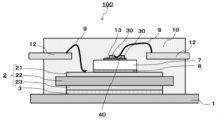
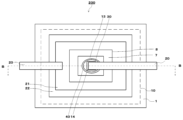
- FIG. 1 is a schematic plan view showing a semiconductor device according to a first embodiment
- FIG. 1 is a cross-sectional structural schematic diagram showing a semiconductor device according to a first embodiment
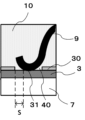
- FIG. FIG. 2 is a cross-sectional structural schematic diagram showing an enlarged joint portion of a wiring portion of the semiconductor device in Embodiment 1
- 2 is a schematic plan view showing a covering portion of the semiconductor device according to Embodiment 1
- FIG. FIG. 2 is a perspective structural schematic diagram showing a covering portion of the semiconductor device in Embodiment 1
- 3 is a schematic plan view showing another covering portion of the semiconductor device according to the first embodiment
- FIG. 3 is a schematic plan view showing another covering portion of the semiconductor device according to the first embodiment
- FIG. 1 is a schematic plan view showing a semiconductor device according to a first embodiment
- FIG. 1 is a cross-sectional structural schematic diagram showing a semiconductor device according to a first embodiment
- FIG. 2 is a cross-sectional structural schematic diagram showing an enlarged joint portion of
- FIG. 3 is a schematic plan view showing another covering portion of the semiconductor device according to the first embodiment;
- FIG. 3 is a schematic plan view showing another covering portion of the semiconductor device according to the first embodiment;
- FIG. 10 is a perspective structural schematic diagram showing another covering portion of the semiconductor device in Embodiment 1;
- FIG. 10 is a perspective structural schematic diagram showing another covering portion of the semiconductor device in Embodiment 1;
- FIG. 10 is a schematic plan view showing a semiconductor device according to a second embodiment;
- FIG. 10 is a schematic cross-sectional view showing a semiconductor device according to a second embodiment;
- FIG. 10 is a cross-sectional structural schematic diagram showing an enlarged joint portion of a wiring portion of a semiconductor device according to a second embodiment;
- FIG. 12 is a block diagram showing the configuration of a power conversion system to which a power conversion device according to Embodiment 3 is applied;
- FIG. 1 is a schematic plan view showing a semiconductor device according to Embodiment 1.
- FIG. 2 is a schematic cross-sectional view showing the semiconductor device according to the first embodiment.
- FIG. 3 is a cross-sectional structural schematic diagram showing an enlarged junction portion of the wiring portion of the semiconductor device according to the first embodiment.
- a semiconductor device 100 includes a base plate 1, an insulating substrate 2, an element bonding portion 8 that is a bonding portion, a substrate bonding portion 3 that is a bonding portion, a semiconductor element 7, a wiring portion 9, It includes a sealing portion 10 , an electrode terminal 12 , an electrode 13 , a covering portion 30 , and an opening portion 40 surrounded by the covering portion 30 .
- FIG. 2 is a cross-sectional structure schematic diagram in the dashed-dotted line AA of FIG.
- the semiconductor device 100 has the upper surface of the base plate 1 and the lower surface of the insulating substrate 2 joined together using the substrate joint portion 3 .
- the upper surface of the insulating substrate 2 and the back surface (lower surface) of the semiconductor element 7 are bonded using the element bonding portion 8 .
- the insulating substrate 2 and the semiconductor element 7 and the wiring portion 9 bonded to the upper surface of the insulating substrate 2 are sealed in the sealing portion 10 .
- the sealing portion 10 is indicated by a dotted line so that the positional relationship of the members sealed in the sealing portion 10 can be understood.
- the outermost periphery of the semiconductor device 100 is the periphery of the base plate 1 .
- a sealing portion 10 is arranged inside the peripheral portion of the base plate 1 .
- An insulating layer 22 of the insulating substrate 2 is arranged inside the outer edge of the sealing portion 10 .
- the metal layer 21 on the upper surface side of the insulating substrate 2 is arranged inside the outer edge of the insulating layer 22 of the insulating substrate 2 .
- a semiconductor element 7 having an electrode 13 formed thereon is arranged inside the outer edge of the metal layer 21 on the upper surface side of the insulating substrate 2 .
- a covering portion 30 having an opening 40 is arranged inside the outer edge of the electrode 13 of the semiconductor element 7 .
- the opening 40 is a region surrounded by the covering portion 30 having a predetermined width.
- the wiring portion 9 is joined to the electrode 13 with a gap from the inner edge of the covering portion 30 .
- the electrode terminal 12 is arranged across the insulating substrate 2 and protrudes (exposed) from the sealing portion 10 .
- the upper surface of the base plate 1 and the lower surface of the metal layer 23 on the lower surface side of the insulating substrate 2 are joined using the substrate joint portion 3 .
- the upper surface of the metal layer 21 on the upper surface side of the insulating substrate 2 and the back surface of the semiconductor element 7 are bonded using the element bonding portion 8 .
- the wiring portion 9 electrically connects the electrode 13 on the surface (upper surface) of the semiconductor element 7 and the electrode terminal 12 (on the right side).
- the sealing portion 10 is in contact with the upper surface of the base plate 1 that is not bonded (exposed) to the metal layer 23 on the lower surface side of the insulating substrate 2 , and the insulating substrate 2 and the semiconductor element 7 bonded to the upper surface of the insulating substrate 2 . and are sealed.
- the electrode terminal 12 is arranged above the insulating substrate 2 so that one end side is arranged inside the sealing portion 10 and the other end side is exposed (protrudes) from the side surface of the sealing portion 10 .
- the electrode 13 arranged on the surface of the semiconductor element 7 and the wiring portion 9 are joined at the joint portion 31 .
- the covering portion 30 surrounds the joint portion 31 .
- the inner side surrounded by the covering portion 30 is the opening portion 40 .
- the outer edge (peripheral portion) of the joint portion 31 and the inner edge (inner peripheral portion) of the covering portion 30 are arranged with a gap (interval) S therebetween.
- the sealing portion 10 is arranged in contact with the surface of the electrode 13 in the gap S portion. Further, the sealing portion 10 is arranged in contact with the surface of the covering portion 30 outside the gap S (outside the inner edge of the covering portion 30).
- the inner peripheral portion of the covering portion 30 is the outer edge of the opening portion 40 .
- the base plate 1 is plate-shaped and serves as the bottom portion (bottom plate) of the semiconductor device 100 .
- the base plate 1 functions as a heat dissipation member that dissipates heat generated inside the semiconductor device 100 to the outside of the semiconductor device 100 .
- the upper surface of the base plate 1 is joined to the lower surface of the metal layer 23 on the lower surface side of the insulating substrate 2 via (using) the substrate joint portion 3 .
- a copper alloy, an aluminum alloy, or the like can be used as a material for the base plate 1.
- the lower surface of the sealing portion 10 is in contact with the outer side of the bonding area between the base plate 1 and the substrate bonding portion 3 .
- the insulating substrate 2 has an upper surface layer, an intermediate layer and a lower surface layer.
- a metal layer 23 on the lower surface side of the insulating substrate 2 faces the upper surface of the base plate 1 .
- the insulating substrate 2 has an insulating layer 22 as an intermediate layer, a metal layer 21 on the upper surface side of the insulating layer 22 as an upper surface layer, and a metal layer 23 on the lower surface side of the insulating layer 22 as a lower surface layer.
- a metal layer 23 on the lower surface side of the insulating layer 22 is joined to the upper surface of the base plate 1 by the substrate joint portion 3 .
- the insulating substrate 2 is plate-shaped, and when the plate-shaped insulating substrate 2 is viewed from the plane (upper surface) direction, the size of the metal layer 21 on the upper surface side of the insulating layer 22 is the same as that of the insulating layer 22 sandwiched therebetween.
- the size of the metal layer 21 on the upper surface side of the layer 22 is larger than the size of the insulating layer 22 in order to suppress creeping discharge (ensure a creepage distance) between the metal layer 23 on the lower surface side of the insulating layer 22 and the base plate 1 . It's getting smaller.
- the end portion of the insulating layer 22 protrudes outward from the end portions of the metal layer 21 on the upper surface side of the insulating layer 22 and the metal layer 23 on the lower surface side of the insulating layer 22 .
- the metal layer 21 on the upper surface side of the insulating layer 22 may be divided into a plurality of parts depending on the purpose to form a circuit pattern.
- a material for the insulating layer 22 of the insulating substrate aluminum oxide ( Al2O3 ), aluminum nitride ( AlN ), silicon nitride ( Si3N4 ), or the like can be used.
- a material for the metal layer 21 on the upper surface side and the metal layer 23 on the lower surface side of the insulating substrate 2 a copper alloy, an aluminum alloy, or the like can be used.
- a semiconductor element 7 is bonded to the upper surface of the metal layer 21 on the upper surface side of the insulating substrate 2 at an element bonding portion 8 .
- the upper surface side of the insulating substrate 2 is synonymous with the upper surface side of the insulating layer 22
- the lower surface side of the insulating substrate 2 is synonymous with the lower surface side of the insulating layer 22 .
- the substrate bonding portion 3 is a bonding material for bonding the upper surface of the base plate 1 and the lower surface of the metal layer 23 on the lower surface side of the insulating substrate 2 .
- Solder is used as the material of the substrate joint portion 3, and sintered silver, sintered copper, or the like may be used as necessary.
- An insulating substrate 2 is bonded to the central region of the base plate 1 .
- the element bonding portion 8 is a bonding material for bonding the upper surface of the metal layer 21 on the upper surface side of the insulating substrate 2 and the back surface of the semiconductor element 7 .
- Solder, sintered silver, sintered copper, or the like can be used as the material of the element joint portion 8 as in the case of the substrate joint portion 3 .
- the semiconductor element 7 has an electrode 13 arranged on the surface of the semiconductor element 7 .
- the semiconductor element 7 is bonded to the upper surface of the metal layer 21 on the upper surface side of the insulating substrate 2 via an element bonding portion 8 which is a bonding portion.
- the semiconductor element 7 can be a power semiconductor element such as a MOSFET (Metal Oxide Semiconductor Field Effect Transistor) or an IGBT (Insulated Gate Bipolar Transistor). Silicon (Si: Silicon), silicon carbide (SiC: Silicon Carbide), or the like can be used as the material of the semiconductor element 7 .
- MOSFET Metal Oxide Semiconductor Field Effect Transistor
- IGBT Insulated Gate Bipolar Transistor
- the electrodes 13 are for electrically connecting the semiconductor element 7 to the outside, and are connected to the wiring portion 9 and the like.
- a material of the electrode 13 Al, an Al alloy containing Si, Cu, or the like can be used.
- the material of the electrode 13 can be appropriately selected according to the selection of the material of the wiring portion 9 .
- the left (first) wiring portion 9 electrically connects a predetermined position of the metal layer 21 on the upper surface side of the insulating substrate 2 and the electrode terminal 12 .
- One end side of the left wiring portion 9 is joined to a predetermined position of the metal layer 21 .
- the other end side of the left wiring portion 9 is connected to one end side of the left (first) electrode terminal 12 .
- the right (second) wiring portion 9 electrically connects the electrode 13 on the surface of the semiconductor element 7 and the electrode terminal 12 .
- One end side of the wiring portion 9 on the right side is joined to the electrode 13 of the semiconductor element 7 .
- the other end of the wiring portion 9 on the right side is joined to one end side of the electrode terminal 12 on the right side (second).
- the wiring section 9 electrically connects the plurality of semiconductor elements 7 .
- the wiring part 9 an aluminum alloy wire, a copper alloy wire, a gold wire, a copper alloy lead, an aluminum alloy ribbon, a copper alloy ribbon, or the like can be used. Wires, leads, ribbons, etc. whose surfaces are plated with nickel, gold, silver, tin or the like may also be used.
- the covering portion 30 is formed on the surface of the electrode 13 .
- the covering portion 30 has a predetermined width.
- a region surrounded by the covering portion 30 is an opening portion 40 of the covering portion 30 .
- Polyimide, polyetheramide, polyamideimide, or the like, for example, can be used as the material of the covering portion 30 .
- the purpose of the covering portion 30 is to reduce or suppress the influence of thermal stress caused by heat generation at the electrodes 13 of the semiconductor element 7 .
- the purpose of the covering portion 30 is to improve the adhesion between the sealing portion 10 and the electrode 13 .
- the modulus of elasticity of the covering portion 30 a member having a modulus of elasticity lower than that of the sealing portion 10 can be used.
- a member having a bonding strength between the covering portion 30 and the sealing portion 10 that is higher than the bonding strength between the electrode 13 and the sealing portion 10 can be used.
- thermal stress between the electrode 13 and the sealing portion 10 can be reduced, and peeling of the sealing portion 10 at the electrode 13 can be suppressed.
- the electrode terminals 12 are arranged across the sides of the insulating substrate 2 and protrude (expose) from the sealing portion 10 to the outside.
- the wiring portion 9 electrically connects the electrodes 13 on the upper surface (surface) of the semiconductor element 7 and the electrode terminals 12 . Moreover, the wiring portion 9 electrically connects a predetermined position of the metal layer 21 on the upper surface side of the insulating substrate 2 and the electrode terminal 12 .
- the sealing portion 10 is in contact with the upper surface of the base plate 1 that is not bonded (exposed) to the metal layer 23 on the lower surface side of the insulating substrate 2 , and is bonded to the wiring portion 9 , the insulating substrate 2 , and the upper surface of the insulating substrate 2 .
- the semiconductor element 7 is sealed.
- One end of the electrode terminal 12 is arranged inside the sealing portion 10 , and the other end thereof is arranged so as to be exposed (projected) to the outside from the side surface of the sealing portion 10 .
- the sealing portion 10 seals the insulating substrate 2, the semiconductor element 7, and a part (one end side) of the electrode terminal 12.
- epoxy resin containing a filler such as silicone gel or silica can be used.
- the thermal stress generated between the electrode 13 and the sealing portion 10 can be reduced by the covering portion 30 formed on the upper surface of the electrode 13 .
- the adhesion between the sealing portion 10 and the electrode 13 can be improved, and the reliability of the semiconductor device 100 can be improved.
- the covering portion 30 is formed on the electrode 13 around the joint portion 31 between the wiring portion 9 and the surface of the electrode 13 so as not to contact the wiring portion 9 .
- the formation range of the covering portion 30 may be only the vicinity of the joint portion 31 or the entire surface of the electrode 13 other than the joint portion 31 as long as it does not come into contact with the wiring portion 9 .
- the covering portion 30 is close enough to contact the joint portion 31 of the wiring portion 9 and the electrode 13
- highly accurate positioning is required to avoid the covering portion 30 and join the wiring portion 9 to the upper surface of the electrode 13. becomes. Therefore, the degree of difficulty in forming the junction between the wiring portion 9 and the electrode 13 is increased.
- the distance between the bonding portion 31 of the wiring portion 9 and the covering portion 30 is, for example, 20 ⁇ m or more and 50 ⁇ m. The following range is desirable.
- the shape of the opening 40 of the covering portion 30 may be a shape following the shape of the joint portion 31, such as an ellipse or a square.
- the outer edge shape of the covering portion 30 may be a shape corresponding to the shape of the joint portion 31, such as an elliptical shape or a square shape.
- the interval (distance) between the wiring portion 9 and the inner peripheral portion of the covering portion 30 is 20 ⁇ m or more and 50 ⁇ m or less.
- a surface treatment may be performed to locally roughen the surface of the electrode 13 by laser irradiation or the like in the gap S on the surface of the electrode 13 in the range of 20 ⁇ m or more and 50 ⁇ m or less inside from the inner peripheral portion of the covering portion 30 .
- FIG. 4 to 11 show various shapes of the covering portion 30.
- FIG. FIG. 4 is a schematic plan view showing the covering portion of the semiconductor device according to the first embodiment.
- FIG. 5 is a perspective structural schematic diagram showing the covering portion of the semiconductor device according to the first embodiment.
- 6 is a schematic plan view showing another covering portion of the semiconductor device according to the first embodiment.
- FIG. 7 is a schematic plan view showing another covering portion of the semiconductor device according to the first embodiment.
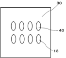
- FIG. 8 is a schematic plan view showing another covering portion of the semiconductor device according to the first embodiment.
- 9 is a schematic plan view showing another covering portion of the semiconductor device according to the first embodiment.
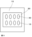
- FIG. FIG. 10 is a perspective structural schematic diagram showing another covering portion of the semiconductor device according to the first embodiment.
- FIG. 11 is a perspective structural schematic diagram showing another covering portion of the semiconductor device according to the first embodiment.
- the covering portion 30 has a belt-like shape.
- the covering portion 30 has a predetermined width and is arranged in advance so as to surround a position where the wiring portion 9 on the upper surface of the electrode 13 is to be joined.
- a region surrounded by the covering portion 30 is the opening portion 40 .
- a plurality of covering portions 30 are arranged on the upper surface of the electrode 13 in an elliptical shape at predetermined intervals.
- the electrode 13 is exposed in the elliptical interior (opening 40 ) of the cover 30 .
- the wiring portion 9 is joined to the upper surface of the electrode 13 exposed in the opening portion 40 .
- the electrode 13 is exposed outside the outer peripheral portion of the covering portion 30 .
- the wiring part 9 is joined to the upper surface of the electrode 13 in the opening part 40 inside the inner peripheral part (inner part) of the covering part 30 .
- a joint portion 31 is a joint portion between the upper surface of the electrode 13 and the wiring portion 9 .
- the joint portion 31 is formed with a predetermined gap from the inner peripheral portion of the covering portion 30 .
- FIG. 6 shows another form of the covering portion 30.
- the elliptical covering portion 30 is arranged such that a plurality of covering portions 30 are partially overlapped (in contact with each other). Also in this case, the opening 40 inside the inner peripheral portion of each covering portion 30 is provided with a region where the wiring portion 9 is bonded to the upper surface of the electrode 13 . The electrode 13 is exposed outside the outer peripheral portion of the covering portion 30 .
- the shape of the covering portion 30 is a rectangle whose area is smaller than the top surface of the electrode 13 .
- the covering portion 30 has an opening 40 which is an oval-shaped region without the covering portion 30 inside the outer edge of the covering portion 30 .
- the upper surface of the electrode 13 is exposed within the opening 40 surrounded by the cover 30 .
- the opening 40 is a region where the upper surface of the electrode 13 and the wiring portion 9 are joined.
- the inner edge shape of the covering portion 30 is different from the outer edge shape of the covering portion 30 .
- the covering portion 30 is formed up to the outer edge of the electrode 13 . In other respects, it has the same shape as the covering portion 30 shown in FIG. A plurality of openings 40 are provided in the cover 30 .
- the covering portion 30 has a belt-like shape. However, unlike FIG. 4, the inner edge (inner peripheral portion) of the covering portion 30 is quadrangular (rectangular). An opening 40 is provided inside the cover 30 . The upper surface of the electrode 13 is exposed at the opening 40 . The wiring part 9 is joined to the exposed upper surface of the electrode 13 . In this case, one or a plurality of wiring portions 9 are joined inside the inner peripheral portion of the covering portion 30 . The number of wiring portions 9 can be appropriately selected according to the specifications (current density, etc.) of the semiconductor device 100 .
- FIG. 10 shows a state in which a plurality of wiring portions 9 are joined inside the covering portion 30 of FIG.
- the wiring portion 9 is joined to the upper surface of the electrode 13 with a gap from the inner peripheral portion of the covering portion 30 to the inner opening portion 40 .
- the outer edge of the band-shaped covering portion 30 shown in FIG. 9 is expanded to the same area as the outer edge of the electrode 13.
- the wiring portion 9 is joined to the opening portion 40 inside the inner peripheral portion of the covering portion 30 in the same manner as in the case of FIG.
- the size increases, and the reliability of the semiconductor device 100 improves.
- the electrodes 13 are formed at predetermined positions on the surface of the semiconductor wafer by, for example, sputtering (electrode forming step).
- the covering portion 30 is formed on the electrode 13 (covering portion forming step).
- the covering portion 30 is made of, for example, photosensitive polyimide, it can be formed by a method described later.
- an appropriate amount of photosensitive polyimide is applied on the electrode 13 by, for example, dispensing.
- a uniform film is formed on the entire surface of the electrode 13 by a spin coater.
- UV (ultraviolet) irradiation is performed from above the mask having openings only for the portions to be formed, whereby the polyimide corresponding to the portions below the openings of the mask can be cured.
- UV irradiation, development, washing, and removal of uncured polyimide can form the covering portion 30 only on a predetermined portion.
- the inner side surrounded by the covering portion 30 is the opening portion 40 .
- the semiconductor wafer described above is diced into small pieces to fabricate semiconductor elements 7 having covering portions 30 formed on the electrodes 13 (semiconductor element preparation step).
- an insulating substrate 2 having a metal layer 21 on the upper surface and a metal layer 23 on the lower surface is prepared (insulating substrate preparation step).
- the insulating layer 22, the metal layer 21 on the upper surface side, and the metal layer 23 on the lower surface side are joined by brazing or the like. Since an electric circuit is formed on the metal layer 21 on the upper surface side, the pattern shape is often different. In such a case, by adjusting the size and thickness of the metal layer 21 on the upper surface side and the metal layer 23 on the lower surface side, generation of thermal stress between the upper and lower (front and back) surfaces of the insulating layer 22 can be suppressed. can be
- the diced semiconductor element 7 is bonded to a predetermined position of the metal layer 21 on the upper surface side of the insulating substrate 2 via the element bonding portion 8 (semiconductor element bonding step).
- base plate 1 that will be the bottom surface of the semiconductor device 100 is prepared (base plate preparation step).
- the insulating substrate 2 is bonded to the upper surface of the base plate 1 at the substrate bonding portion 3 (insulating substrate bonding step).
- the semiconductor element 7 and the metal layer 21 on the upper surface side of the insulating substrate 2 are electrically connected using the wiring portion 9 (wiring material forming step).
- the wiring part 9 is a wire, a ribbon, or a lead, it can be joined using an ultrasonic joining method.
- the insulating substrate 2, the semiconductor element 7, the wiring portion 9, and one end side of the electrode terminal 12 are sealed with the sealing portion 10 (sealing step).
- the semiconductor device 100 shown in FIG. 2 can be manufactured through the above main manufacturing processes.
- the covering portion 30 is formed on the electrode 13 around the joint portion 31 between the wiring portion 9 and the electrode 13 without contacting the wiring portion 9.
- the peeling of the sealing portion 10 when the device 100 is energized can be suppressed, and the reliability of the semiconductor device 100 can be improved. Also, the life of the semiconductor device 100 can be extended.
- the covering portion 30 is formed before the wiring portion 9 and the electrode 13 are joined, the state of formation of the covering portion 30 can be easily inspected, and the process cost can be reduced.
- Embodiment 2 differs from Embodiment 1 in that the wiring portion 9 used in Embodiment 1 is replaced with an electrode terminal 20 having a structure in which one end of the electrode terminal 20 is extended and integrated as a wiring portion.
- the wiring portion 9 used in Embodiment 1 is replaced with an electrode terminal 20 having a structure in which one end of the electrode terminal 20 is extended and integrated as a wiring portion.
- FIG. 12 is a schematic plan view showing the semiconductor device according to the second embodiment.
- FIG. 13 is a schematic cross-sectional view showing the semiconductor device according to the second embodiment.
- FIG. 14 is a cross-sectional structural schematic diagram showing an enlarged junction portion of the wiring portion of the semiconductor device according to the second embodiment.
- a semiconductor device 200 includes a base plate 1, an insulating substrate 2, an element bonding portion 8 that is a bonding portion, a substrate bonding portion 3 that is a bonding portion, a semiconductor element 7, a sealing portion 10, and an electrode. 13 , a terminal joint portion 14 , an electrode terminal 20 that is a wiring portion, a covering portion 30 , and an opening portion 40 surrounded by the covering portion 30 .
- FIG. 13 is a schematic cross-sectional view along the dashed-dotted line BB in FIG. 12 .
- the semiconductor device 200 has the upper surface of the base plate 1 and the lower surface of the insulating substrate 2 joined together using the substrate joining portion 3 .
- the upper surface of the insulating substrate 2 and the back surface (lower surface) of the semiconductor element 7 are bonded using the element bonding portion 8 .
- the insulating substrate 2 , the semiconductor element 7 bonded to the upper surface of the insulating substrate 2 , and one end side of the electrode terminal 20 having a plate-like shape at one end are sealed in the sealing portion 10 .
- the electrode terminal 20 may be a lead frame as long as it can be connected to the electrode 13 .
- the sealing portion 10 is indicated by dotted lines so that the positional relationship of the members sealed in the sealing portion 10 can be understood.
- the outermost periphery of the semiconductor device 200 is the periphery of the base plate 1 .
- a sealing portion 10 is arranged inside the peripheral portion of the base plate 1 .
- An insulating layer 22 of the insulating substrate 2 is arranged inside the outer edge of the sealing portion 10 .
- the metal layer 21 on the upper surface side of the insulating substrate 2 is arranged inside the outer edge of the insulating layer 22 of the insulating substrate 2 .
- a semiconductor element 7 having an electrode 13 formed thereon is arranged inside the outer edge of the metal layer 21 on the upper surface side of the insulating substrate 2 .
- a covering portion 30 having an opening 40 is arranged inside the outer edge of the electrode 13 of the semiconductor element 7 .
- the opening 40 is a region surrounded by the covering portion 30 having a predetermined width.
- One end of the electrode terminal 20 extends inside the inner edge of the covering portion 30 with a gap from the inner edge of the covering portion 30, and the one end of the electrode terminal 20 and the electrode 13 are joined.
- One end of the electrode terminal 20 extends across the insulating substrate 2 to the top of the semiconductor element 7 , and the other end protrudes (exposes) from the sealing portion 10 .
- the other electrode terminal 20 is arranged so that one end of the electrode terminal 20 straddles the insulating substrate 2 and extends to the top of the metal layer 21 on the upper surface side of the insulating substrate 2 , and the other end projects from the sealing portion 10 . (exposed).
- the upper surface of the base plate 1 and the lower surface of the metal layer 23 on the lower surface side of the insulating substrate 2 are joined using the substrate joint portion 3 .
- the upper surface of the metal layer 21 on the upper surface side of the insulating substrate 2 and the back surface of the semiconductor element 7 are bonded using the element bonding portion 8 .
- One end of the right (second) electrode terminal 20 is electrically connected to the electrode 13 on the surface (upper surface) of the semiconductor element 7 via the terminal joint portion 14 .
- One end of the left (first) electrode terminal 20 is electrically connected to the metal layer 21 on the upper surface side of the insulating substrate 2 via the terminal joint portion 14 .
- the sealing portion 10 is in contact with the upper surface of the base plate 1 that is not bonded (exposed) to the metal layer 23 on the lower surface side of the insulating substrate 2 , and the insulating substrate 2 and the semiconductor element 7 bonded to the upper surface of the insulating substrate 2 . and are sealed.
- Each of the electrode terminals 20 has one end disposed inside the sealing portion 10 and the other end exposed (projecting) from the side surface of the sealing portion 10 .
- the electrode 13 arranged on the surface of the semiconductor element 7 and one end of the electrode terminal 20 are joined to each other by the joint portion 32 on the electrode 13 via the terminal joint portion 14 .
- the joint portion 32 is a joint portion between the upper surface of the electrode 13 and the lower surface of the terminal joint portion 14 .
- a joint portion 33 is a joint portion between the lower surface of one end of the electrode terminal 20 and the upper surface of the terminal joint portion 14 .
- the covering portion 30 surrounds the joint portion 32 .
- a region surrounded by the covering portion 30 is an opening portion 40 .
- the outer edge (peripheral portion) of the joint portion 32 and the inner edge (inner peripheral portion) of the covering portion 30 are arranged with a gap (interval) S therebetween.
- the sealing portion 10 is arranged in contact with the surface of the electrode 13 in the gap S portion. Further, the sealing portion 10 is arranged in contact with the surface of the covering portion 30 outside the gap S (outside the inner edge of the covering portion 30).
- the interval (distance) between the outer edge of the joint portion 32 and the inner peripheral portion of the covering portion 30 is 20 ⁇ m or more and 50 ⁇ m or less.
- the gap S on the surface of the electrode 13 in the range of 20 ⁇ m or more and 50 ⁇ m or less inside the inner peripheral portion of the covering portion 30 may be subjected to surface treatment to prevent the terminal joint portion 14 from wetting and spreading.
- the surface treatment the surface of the electrode 13 is locally roughened by laser irradiation or the like. By performing this surface treatment, it is possible to suppress the contact between the inner peripheral portion of the covering portion 30 and the terminal joint portion 14, and the contact between the surface of the electrode 13 subjected to the surface treatment and the sealing portion 10 prevents sealing.
- the stopper portion 10 can be prevented from peeling off. In this way, by surface-treating the region inside the inner peripheral portion of the covering portion 30 of the electrode 13, the adhesion between the sealing portion 10 and the electrode 13 is improved while preventing the terminal joint portion 14 from wetting and spreading. can be improved.
- the electrode terminal 20 is arranged across the side portion of the insulating substrate 2 , and the other end of the electrode terminal 20 protrudes (exposes) from the sealing portion 10 to the outside. One end of the electrode terminal 20 is sealed inside the sealing portion 10 . One end of the electrode terminal 20 on the right side is electrically connected to the electrode 13 on the surface (upper surface) of the semiconductor element 7 via the terminal joint portion 14 . One end of the left electrode terminal 20 is electrically connected to a predetermined position of the metal layer 21 on the upper surface side of the insulating substrate 2 via the terminal joint portion 14 .
- the sealing portion 10 is in contact with the upper surface of the base plate 1 that is not joined (exposed) to the metal layer 23 on the lower surface side of the insulating substrate 2 , and the one end side of the electrode terminal 20 , the insulating substrate 2 , and the upper surface of the insulating substrate 2 . It seals the semiconductor element 7 joined to the .
- a copper alloy lead (lead frame) can be used as the electrode terminal 20 .
- the terminal joint portion 14 is a joint material for joining the upper surface of the electrode 13 and one end side of the electrode terminal 20 .
- Solder, sintered silver, sintered copper, or the like can be used as the material of the terminal joint portion 14, similarly to the board joint portion 3.
- the covering portion 30 is formed on the electrode 13 around the joint portion 32 between the one end of the electrode terminal 20 and the electrode 13 without contacting the one end of the electrode terminal 20 . Therefore, peeling of the sealing portion 10 when the semiconductor device 200 is energized can be suppressed, and the reliability of the semiconductor device 200 can be improved. Also, the life of the semiconductor device 200 can be extended.
- the covering portion 30 is formed before the one end of the electrode terminal 20 and the electrode 13 are joined, the state of formation of the covering portion 30 can be easily inspected, and the process cost can be reduced.
- Embodiment 3 applies the semiconductor devices according to the first and second embodiments described above to a power converter.
- the present disclosure is not limited to a specific power converter, a case where the present disclosure is applied to a three-phase inverter will be described below as a third embodiment.
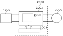
- FIG. 15 is a block diagram showing the configuration of a power conversion system to which the power conversion device according to Embodiment 3 of the present disclosure is applied.
- the power conversion system shown in FIG. 15 includes a power supply 1000, a power conversion device 2000, and a load 3000.
- the power supply 1000 is a DC power supply and supplies DC power to the power converter 2000 .
- the power supply 1000 can be composed of various things, for example, it can be composed of a DC system, a solar battery, a storage battery, or it can be composed of a rectifier circuit connected to an AC system, an AC/DC converter, etc. good.
- power supply 1000 may be configured by a DC/DC converter that converts DC power output from a DC system into predetermined power.
- the power conversion device 2000 is a three-phase inverter connected between the power supply 1000 and the load 3000, converts the DC power supplied from the power supply 1000 into AC power, and supplies the AC power to the load 3000.
- the power conversion device 2000 includes a main conversion circuit 2001 that converts DC power input from a power source 1000 into AC power and outputs the same, and a control signal that controls the main conversion circuit 2001 to the main conversion circuit 2001. and a control circuit 2003 for outputting to.
- a load 3000 is a three-phase electric motor driven by AC power supplied from the power converter 2000 . It should be noted that the load 3000 is not limited to a specific application, but is an electric motor mounted on various electrical equipment, such as hybrid automobiles, electric automobiles, railroad cars, elevators, and electric motors for air conditioners.
- the main conversion circuit 2001 includes a switching element and a freewheeling diode (not shown) built in the semiconductor device 2002. By switching the switching element, the DC power supplied from the power supply 1000 is converted into AC power. and supply it to the load 3000 .
- the main conversion circuit 2001 has various specific circuit configurations, the main conversion circuit 2001 according to the present embodiment is a two-level three-phase full bridge circuit, and has six switching elements and It can be composed of six freewheeling diodes connected in anti-parallel.
- the main conversion circuit 2001 is configured by a semiconductor device 2002 corresponding to any one of the above-described first to fifth embodiments, which incorporates switching elements, freewheeling diodes, and the like.
- each upper and lower arm forms each phase (U phase, V phase, W phase) of the full bridge circuit.
- the output terminals of each upper and lower arm, that is, the three output terminals of main conversion circuit 2001 are connected to load 3000 .
- the main conversion circuit 2001 also includes a drive circuit (not shown) that drives each switching element.
- the driver circuit may be built in the semiconductor device 2002, or may be configured to include a driver circuit separately from the semiconductor device 2002.
- FIG. The drive circuit generates a drive signal for driving the switching element of the main conversion circuit 2001 and supplies it to the control electrode of the switching element of the main conversion circuit 2001 .
- a drive signal for turning on the switching element and a drive signal for turning off the switching element are output to the control electrode of each switching element.
- the driving signal When maintaining the switching element in the ON state, the driving signal is a voltage signal (ON signal) equal to or higher than the threshold voltage of the switching element, and when maintaining the switching element in the OFF state, the driving signal is a voltage equal to or less than the threshold voltage of the switching element. signal (off signal).
- the control circuit 2003 controls the switching elements of the main conversion circuit 2001 so that the desired power is supplied to the load 3000 . Specifically, based on the power to be supplied to the load 3000, the time (on time) during which each switching element of the main converter circuit 2001 should be in the ON state is calculated. For example, the main conversion circuit 2001 can be controlled by PWM control that modulates the ON time of the switching element according to the voltage to be output. In addition, a control command ( control signal). The drive circuit outputs an ON signal or an OFF signal as a drive signal to the control electrode of each switching element according to this control signal.
- the semiconductor device according to the first to fourth embodiments is applied as the semiconductor device 2002 of the main conversion circuit 2001, the reliability is improved. be able to.
- the present disclosure is not limited to this, and can be applied to various power converters.
- a two-level power conversion device is used, but a three-level or multi-level power conversion device may also be used. may apply.
- the present disclosure can be applied to DC/DC converters, AC/DC converters, etc. when power is supplied to a DC load or the like.
- the power conversion device to which the present disclosure is applied is not limited to the case where the above-described load is an electric motor. etc., and furthermore, it can be used as a power conditioner for a photovoltaic power generation system, an electric storage system, and the like.
- the power semiconductor element 7 when SiC is used as the semiconductor element 7, the power semiconductor element is operated at a higher temperature compared to Si in order to take advantage of its characteristics. Since higher reliability is required for semiconductor devices on which SiC devices are mounted, the advantage of the present disclosure that a highly reliable semiconductor device is realized becomes more effective.
Landscapes
- Structures Or Materials For Encapsulating Or Coating Semiconductor Devices Or Solid State Devices (AREA)
Priority Applications (2)
| Application Number | Priority Date | Filing Date | Title |
|---|---|---|---|
| PCT/JP2021/040622 WO2023079640A1 (ja) | 2021-11-04 | 2021-11-04 | 半導体装置および電力変換装置 |
| JP2022518732A JP7176662B1 (ja) | 2021-11-04 | 2021-11-04 | 半導体装置および電力変換装置 |
Applications Claiming Priority (1)
| Application Number | Priority Date | Filing Date | Title |
|---|---|---|---|
| PCT/JP2021/040622 WO2023079640A1 (ja) | 2021-11-04 | 2021-11-04 | 半導体装置および電力変換装置 |
Publications (1)
| Publication Number | Publication Date |
|---|---|
| WO2023079640A1 true WO2023079640A1 (ja) | 2023-05-11 |
Family
ID=84144809
Family Applications (1)
| Application Number | Title | Priority Date | Filing Date |
|---|---|---|---|
| PCT/JP2021/040622 Ceased WO2023079640A1 (ja) | 2021-11-04 | 2021-11-04 | 半導体装置および電力変換装置 |
Country Status (2)
| Country | Link |
|---|---|
| JP (1) | JP7176662B1 (https=) |
| WO (1) | WO2023079640A1 (https=) |
Cited By (1)
| Publication number | Priority date | Publication date | Assignee | Title |
|---|---|---|---|---|
| WO2025022969A1 (ja) * | 2023-07-26 | 2025-01-30 | ローム株式会社 | 半導体装置の製造方法、半導体装置および車両 |
Citations (6)
| Publication number | Priority date | Publication date | Assignee | Title |
|---|---|---|---|---|
| JPH0982851A (ja) * | 1995-09-13 | 1997-03-28 | Matsushita Electron Corp | 半導体装置 |
| JPH11186319A (ja) * | 1997-12-19 | 1999-07-09 | Matsushita Electron Corp | 半導体装置および半導体装置の製造方法 |
| JP2006165515A (ja) * | 2004-11-11 | 2006-06-22 | Denso Corp | 半導体装置およびその製造方法 |
| JP2008294219A (ja) * | 2007-05-24 | 2008-12-04 | Toshiba Corp | 半導体装置及びその製造方法 |
| JP2016028417A (ja) * | 2014-07-11 | 2016-02-25 | ローム株式会社 | 電子装置 |
| JP2020043154A (ja) * | 2018-09-07 | 2020-03-19 | 三菱電機株式会社 | 半導体装置及びその製造方法、並びに、電力変換装置 |
-
2021
- 2021-11-04 WO PCT/JP2021/040622 patent/WO2023079640A1/ja not_active Ceased
- 2021-11-04 JP JP2022518732A patent/JP7176662B1/ja active Active
Patent Citations (6)
| Publication number | Priority date | Publication date | Assignee | Title |
|---|---|---|---|---|
| JPH0982851A (ja) * | 1995-09-13 | 1997-03-28 | Matsushita Electron Corp | 半導体装置 |
| JPH11186319A (ja) * | 1997-12-19 | 1999-07-09 | Matsushita Electron Corp | 半導体装置および半導体装置の製造方法 |
| JP2006165515A (ja) * | 2004-11-11 | 2006-06-22 | Denso Corp | 半導体装置およびその製造方法 |
| JP2008294219A (ja) * | 2007-05-24 | 2008-12-04 | Toshiba Corp | 半導体装置及びその製造方法 |
| JP2016028417A (ja) * | 2014-07-11 | 2016-02-25 | ローム株式会社 | 電子装置 |
| JP2020043154A (ja) * | 2018-09-07 | 2020-03-19 | 三菱電機株式会社 | 半導体装置及びその製造方法、並びに、電力変換装置 |
Cited By (1)
| Publication number | Priority date | Publication date | Assignee | Title |
|---|---|---|---|---|
| WO2025022969A1 (ja) * | 2023-07-26 | 2025-01-30 | ローム株式会社 | 半導体装置の製造方法、半導体装置および車両 |
Also Published As
| Publication number | Publication date |
|---|---|
| JP7176662B1 (ja) | 2022-11-22 |
| JPWO2023079640A1 (https=) | 2023-05-11 |
Similar Documents
| Publication | Publication Date | Title |
|---|---|---|
| JP6399272B1 (ja) | パワーモジュール及びその製造方法並びに電力変換装置 | |
| JP6806170B2 (ja) | 半導体装置及び電力変換装置 | |
| JP6826665B2 (ja) | 半導体装置、半導体装置の製造方法及び電力変換装置 | |
| JP7561677B2 (ja) | 電力半導体装置、電力半導体装置の製造方法及び電力変換装置 | |
| WO2019049400A1 (ja) | パワーモジュール及びその製造方法並びに電力変換装置 | |
| JP6680419B1 (ja) | 半導体装置、半導体装置の製造方法および電力変換装置 | |
| CN111052325B (zh) | 半导体模块以及电力转换装置 | |
| JP7019024B2 (ja) | 半導体装置及び電力変換装置 | |
| JP2021002610A (ja) | 半導体モジュール、車両、および半導体モジュールの製造方法 | |
| WO2020148879A1 (ja) | 半導体装置、半導体装置の製造方法及び電力変換装置 | |
| JP7176662B1 (ja) | 半導体装置および電力変換装置 | |
| JP7134345B2 (ja) | 半導体モジュール、半導体モジュールの製造方法および電力変換装置 | |
| JP2024013569A (ja) | 半導体装置、半導体装置の製造方法および電力変換装置 | |
| JP7555486B2 (ja) | パワー半導体装置及び電力変換装置 | |
| JP7270772B2 (ja) | 半導体装置、電力変換装置および半導体装置の製造方法 | |
| JP6885522B1 (ja) | 半導体装置、電力変換装置および半導体装置の製造方法 | |
| JP7088421B1 (ja) | 半導体装置および電力変換装置 | |
| JP2023013642A (ja) | 半導体装置 | |
| JP7438466B1 (ja) | 半導体装置及びその製造方法並びに電力変換装置 | |
| JP7237192B2 (ja) | 半導体装置およびその製造方法ならびに電力変換装置 | |
| JP7106007B2 (ja) | 半導体装置および電力変換装置 | |
| JP7229382B2 (ja) | 半導体装置、電力変換装置および半導体装置の製造方法 | |
| WO2024090278A1 (ja) | 半導体装置、電力変換装置および半導体装置の製造方法 | |
| WO2025052628A1 (ja) | 半導体装置、半導体装置の製造方法および電力変換装置 | |
| WO2025009015A1 (ja) | パワーモジュール及びその製造方法並びに電力変換装置 |
Legal Events
| Date | Code | Title | Description |
|---|---|---|---|
| WWE | Wipo information: entry into national phase |
Ref document number: 2022518732 Country of ref document: JP |
|
| 121 | Ep: the epo has been informed by wipo that ep was designated in this application |
Ref document number: 21963237 Country of ref document: EP Kind code of ref document: A1 |
|
| NENP | Non-entry into the national phase |
Ref country code: DE |
|
| 122 | Ep: pct application non-entry in european phase |
Ref document number: 21963237 Country of ref document: EP Kind code of ref document: A1 |