WO2023074522A1 - 物理量検出装置及び撮像装置 - Google Patents
物理量検出装置及び撮像装置 Download PDFInfo
- Publication number
- WO2023074522A1 WO2023074522A1 PCT/JP2022/039081 JP2022039081W WO2023074522A1 WO 2023074522 A1 WO2023074522 A1 WO 2023074522A1 JP 2022039081 W JP2022039081 W JP 2022039081W WO 2023074522 A1 WO2023074522 A1 WO 2023074522A1
- Authority
- WO
- WIPO (PCT)
- Prior art keywords
- pixel
- signal
- physical quantity
- pixels
- data
- Prior art date
- Legal status (The legal status is an assumption and is not a legal conclusion. Google has not performed a legal analysis and makes no representation as to the accuracy of the status listed.)
- Ceased
Links
Images











Classifications
-
- H—ELECTRICITY
- H04—ELECTRIC COMMUNICATION TECHNIQUE
- H04N—PICTORIAL COMMUNICATION, e.g. TELEVISION
- H04N25/00—Circuitry of solid-state image sensors [SSIS]; Control thereof
- H04N25/70—SSIS architectures; Circuits associated therewith
- H04N25/76—Addressed sensors, e.g. MOS or CMOS sensors
- H04N25/78—Readout circuits for addressed sensors, e.g. output amplifiers or A/D converters
-
- H—ELECTRICITY
- H04—ELECTRIC COMMUNICATION TECHNIQUE
- H04N—PICTORIAL COMMUNICATION, e.g. TELEVISION
- H04N25/00—Circuitry of solid-state image sensors [SSIS]; Control thereof
- H04N25/70—SSIS architectures; Circuits associated therewith
- H04N25/703—SSIS architectures incorporating pixels for producing signals other than image signals
-
- H—ELECTRICITY
- H04—ELECTRIC COMMUNICATION TECHNIQUE
- H04N—PICTORIAL COMMUNICATION, e.g. TELEVISION
- H04N25/00—Circuitry of solid-state image sensors [SSIS]; Control thereof
- H04N25/70—SSIS architectures; Circuits associated therewith
- H04N25/76—Addressed sensors, e.g. MOS or CMOS sensors
- H04N25/77—Pixel circuitry, e.g. memories, A/D converters, pixel amplifiers, shared circuits or shared components
-
- H—ELECTRICITY
- H04—ELECTRIC COMMUNICATION TECHNIQUE
- H04N—PICTORIAL COMMUNICATION, e.g. TELEVISION
- H04N25/00—Circuitry of solid-state image sensors [SSIS]; Control thereof
- H04N25/70—SSIS architectures; Circuits associated therewith
- H04N25/76—Addressed sensors, e.g. MOS or CMOS sensors
- H04N25/77—Pixel circuitry, e.g. memories, A/D converters, pixel amplifiers, shared circuits or shared components
- H04N25/771—Pixel circuitry, e.g. memories, A/D converters, pixel amplifiers, shared circuits or shared components comprising storage means other than floating diffusion
-
- H—ELECTRICITY
- H04—ELECTRIC COMMUNICATION TECHNIQUE
- H04N—PICTORIAL COMMUNICATION, e.g. TELEVISION
- H04N25/00—Circuitry of solid-state image sensors [SSIS]; Control thereof
- H04N25/70—SSIS architectures; Circuits associated therewith
- H04N25/76—Addressed sensors, e.g. MOS or CMOS sensors
- H04N25/77—Pixel circuitry, e.g. memories, A/D converters, pixel amplifiers, shared circuits or shared components
- H04N25/772—Pixel circuitry, e.g. memories, A/D converters, pixel amplifiers, shared circuits or shared components comprising A/D, V/T, V/F, I/T or I/F converters
-
- H—ELECTRICITY
- H04—ELECTRIC COMMUNICATION TECHNIQUE
- H04N—PICTORIAL COMMUNICATION, e.g. TELEVISION
- H04N25/00—Circuitry of solid-state image sensors [SSIS]; Control thereof
- H04N25/70—SSIS architectures; Circuits associated therewith
- H04N25/76—Addressed sensors, e.g. MOS or CMOS sensors
- H04N25/7795—Circuitry for generating timing or clock signals
-
- H—ELECTRICITY
- H04—ELECTRIC COMMUNICATION TECHNIQUE
- H04N—PICTORIAL COMMUNICATION, e.g. TELEVISION
- H04N25/00—Circuitry of solid-state image sensors [SSIS]; Control thereof
- H04N25/70—SSIS architectures; Circuits associated therewith
- H04N25/79—Arrangements of circuitry being divided between different or multiple substrates, chips or circuit boards, e.g. stacked image sensors
Definitions
- the present disclosure relates to a physical quantity detection device and an imaging device.
- ADC analog-to-digital conversion
- AD conversion analog-to-digital conversion
- pixel data AD-converted at each pixel is transferred to an output unit.
- Pixel data must be transferred within a vertical synchronization period, that is, within one frame period.
- the AD-converted pixel data cannot be transferred to the output section within one frame period, which may cause problems such as deterioration of the image quality of the captured image. be.
- each pixel in the pixel array unit is sometimes used for purposes other than imaging (for example, detection of various physical quantities). Even for the purpose of imaging, the required frame rate and resolution are different between moving image imaging and still image imaging. If image data cannot be transferred in time for one frame period, problems such as failure to detect physical quantities normally occur.
- the present disclosure provides a physical quantity detection device and an imaging device that can prevent the problem of not being able to transfer pixel data in time.
- At least two pixel groups each detecting a physical quantity; a storage unit that stores data corresponding to physical quantities detected by individual pixels in the pixel group;
- a physical quantity detection device comprising: a storage control unit that controls storage of the data in the storage unit and controls whether or not to update the data stored in the storage unit for each pixel group. be done.
- the storage unit may be an analog memory or a digital memory.
- An AD converter may be provided which has the storage unit and converts the physical quantity signal into a digital signal by comparing the physical quantity signal detected for each pixel in the pixel group with a reference signal.
- the storage unit may store the time code according to timing at which the time code and the reference signal match.
- the storage control unit stores, among the at least two pixel groups, pixel groups in which data in the storage unit of all corresponding pixels within the predetermined period cannot be output in the storage unit during the next predetermined period. You may retain the data that has been received without updating it.
- the predetermined period may be the period of the vertical synchronization signal.
- the at least two pixel groups may have different pixel characteristics.
- the pixel characteristics may include at least one of pixel sensitivity and a saturation amount capable of accumulating a physical quantity signal.
- the pixel characteristics may include at least one of phase difference, luminance information, gradation information, color information, event information, environment information, biological information, and sound wave information.
- the pixel characteristics may include a resolution of an AD converter provided for each pixel in the at least two pixel groups.
- the pixel characteristics may include the storage capacity of the storage unit.
- the at least two pixel groups may have different signal detection periods.
- the signal detection period may include at least one of exposure time and signal readout time.
- An interpolation processing unit may be provided that interpolates the physical quantity of a pixel not included in the pixel group with the physical quantity of the pixel in the pixel group located around the pixel.
- a pixel array section having a plurality of pixels divided into the at least two pixel groups; a plurality of control wirings for controlling readout of all pixels in the pixel array section; According to the pixel group to which each pixel in the pixel array section belongs, a contact for connecting each pixel and the corresponding control wiring may be provided.
- the plurality of control wirings are arranged in a region of all pixels in the pixel array section; Each pixel in the pixel array section may be connected to one of the plurality of control lines through the contact.
- the physical quantity may include at least one of light intensity, sound pressure of sound waves, and biological information amount.
- the physical quantity includes light intensity
- the at least two pixel groups may include at least one of a still image capturing area, a moving image capturing area, and an image plane phase difference detecting area.
- a pixel array section having a plurality of pixels, the plurality of pixels being divided into at least two pixel groups; an AD converter that is provided for each pixel and performs analog-to-digital conversion of a pixel signal; a time code generator that generates a time code that changes with time; a reference signal generator that generates a reference signal whose voltage level changes over time; a signal processing unit that performs signal processing on pixel data output from the AD converter for each pixel,
- the AD converter has a storage unit that stores the time code corresponding to the pixel signal by comparing the pixel signal with the reference signal,
- an imaging device further comprising a storage control unit that controls storage of the time code in the storage unit and controls whether or not the time code stored in the storage unit is updated for each pixel group. be done.
- the storage control unit updates the time code in the corresponding storage unit within the next vertical synchronization period for a group of pixels for which pixel data of all pixels could not be transferred to the signal processing unit within the vertical synchronization period. You can keep it without
- FIG. 1 is a diagram showing a schematic configuration of a solid-state imaging device according to the present disclosure
- FIG. 3 is a block diagram showing a detailed configuration example of a pixel
- FIG. 3 is a block diagram showing a detailed configuration example of a comparison circuit
- FIG. 4 is a diagram showing transition of each signal during operation of the comparison circuit
- 4A and 4B are diagrams for explaining a detailed configuration of a pixel circuit
- FIG. 4 is a timing chart for explaining pixel operations
- FIG. 4 is a circuit diagram showing an example of a configuration without a time code transfer section and a data storage section
- 4 is a circuit diagram showing internal configurations of a P-phase bit storage unit and a D-phase bit storage unit
- FIG. 4 is a circuit diagram showing an example in which a latch circuit is configured using an analog memory
- FIG. 4 is a diagram showing an example of a pixel group in a pixel array section; The figure which shows the example of a changed completely type of FIG. 9A.
- FIG. 4 is a diagram showing, by arrows, the order in which pixel data of each pixel in the first pixel group is read
- FIG. 10 is a diagram showing the readout order of pixel data of the second pixel group with arrows
- FIG. 10 is a diagram showing the readout order of pixel data of the third pixel group with arrows
- FIG. 13B is a diagram following FIG. 13A.
- FIG. 13B The figure following FIG. 13C.
- FIG. 4 is a timing chart of the imaging device 1 according to this embodiment;
- FIG. 4 The figure which shows the typical example of an interpolation process.
- FIG. 4 is a diagram showing an example of an imaging device configured by laminating a pixel substrate and a logic substrate;
- 1 is a block diagram showing an example of a schematic configuration of a vehicle control system;
- FIG. FIG. 2 is an explanatory diagram showing an example of installation positions of an information detection unit outside the vehicle and an imaging unit;
- An imaging device will be mainly described below as an example of a physical quantity detection device, but as will be described later, the physical quantity detection device of the present disclosure is not necessarily limited to an imaging device.
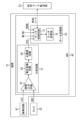
- FIG. 1 shows a schematic configuration of an imaging device 1 according to the present disclosure.
- the imaging device 1 formed on a semiconductor substrate will be mainly described below.
- This type of imaging device 1 is also called a solid-state imaging device 1, but will be simply referred to as the imaging device 1 below.
- the imaging device 1 of FIG. 1 has a pixel array section 22 in which pixels 21 are arranged in a two-dimensional array on a semiconductor substrate 11 using, for example, silicon (Si) as a semiconductor.
- the pixel array section 22 is provided with a time code transfer section 23 that transfers the time code generated by the time code generation section 26 to each pixel 21 .
- a pixel driving circuit 24 Around the pixel array section 22 on the semiconductor substrate 11, there are a pixel driving circuit 24, a DAC (D/A converter, reference signal generating section) 25, a time code generating section 26, a vertical driving circuit 27, an output section 28, and a timing generation circuit 29 are formed.
- FIG. 2 is a block diagram showing the configuration of each pixel 21 arranged in a two-dimensional array in the pixel array section 22.
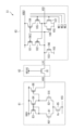
- FIG. Each pixel 21 has a pixel circuit 41 and an ADC 42, as shown in FIG.
- Each pixel 21 generates a charge signal corresponding to the amount of light received by a light receiving element (for example, a photodiode) in the pixel, converts it into a digital pixel signal, and outputs it.
- a light receiving element for example, a photodiode
- the pixel drive circuit 24 in FIG. 1 drives the pixel circuit 41 (FIG. 2) in the pixel 21.
- the DAC 25 generates a reference signal (reference voltage signal) REF, which is a slope signal whose level (voltage) monotonously decreases with time, and supplies it to each pixel 21 .
- the time code generation unit 26 generates a time code used when each pixel 21 converts the analog pixel signal SIG into a digital pixel signal (AD conversion), and supplies the generated time code to the corresponding time code transfer unit 23 . .
- a plurality of time code generators 26 are provided in the pixel array section 22 , and the number of time code transfer sections 23 corresponding to the number of time code generators 26 is provided in the pixel array section 22 . That is, the time code generating section 26 and the time code transfer section 23 for transferring the time code generated therein correspond one-to-one.
- the vertical drive circuit 27 controls output of the digital pixel signals generated in the pixels 21 to the output unit 28 through the time code transfer unit 23 in a predetermined order based on the timing signal supplied from the timing generation circuit 29. I do.
- a digital pixel signal output from the pixel 21 is output from the output unit 28 to the outside of the imaging device 1 .
- the output unit 28 performs predetermined digital signal processing such as black level correction processing for correcting the black level and CDS (Correlated Double Sampling) processing as necessary, and then outputs to the outside. In this way, the output unit 28 has built-in functions for performing various kinds of arithmetic processing and signal processing.
- the timing generation circuit 29 has a timing generator for generating various timing signals, and supplies the generated various timing signals to the pixel drive circuit 24, the DAC 25, the vertical drive circuit 27, and the like.
- the imaging device 1 has the configuration described above. In FIG. 1, as described above, all the circuits forming the imaging device 1 are formed on the single semiconductor substrate 11. However, as will be described later, the circuits forming the imaging device 1 can be arranged separately on a plurality of semiconductor substrates 11 .
- the pixel 21 has a pixel circuit 41 and an ADC (AD converter) 42 .
- the imaging device 1 according to the present embodiment is a pixel ADC type imaging device 1 in which each pixel has the ADC 42 .
- the pixel circuit 41 outputs a charge signal corresponding to the amount of received light to the ADC 42 as an analog pixel signal SIG.
- the ADC 42 converts the analog pixel signal SIG supplied from the pixel circuit 41 into a digital pixel signal.
- ADC 42 has comparison circuit 51 and data storage unit 52 .
- the comparison circuit 51 compares the reference signal REF supplied from the DAC 25 and the pixel signal SIG, and outputs the output signal VCO as a comparison result signal representing the comparison result.
- the comparison circuit 51 inverts the potential of the output signal VCO when the reference signal REF and the pixel signal SIG are the same (at the same voltage).
- the comparison circuit 51 has a differential input circuit 61 , a voltage conversion circuit 62 , and a positive feedback circuit (PFB: positive feedback) 63 .
- PFB positive feedback circuit
- the data storage unit 52 receives the output signal VCO from the comparison circuit 51, and also receives a WR signal (hereinafter also referred to as a write control signal WR) from the vertical drive circuit 27, which indicates a pixel signal write operation.
- a WR signal hereinafter also referred to as a write control signal WR
- An RD signal (hereinafter also referred to as a readout control signal RD) representing a pixel signal readout operation and a WORD signal controlling the readout timing of the pixels 21 during the pixel signal readout operation are supplied from the vertical drive circuit 27. supplied.
- the data storage unit 52 is also supplied with the time code generated by the time code generation unit 26 via the time code transfer unit 23 .
- the data storage unit 52 has a latch control circuit (storage control unit) 71 that controls the write operation and read operation of the time code based on the WR signal and the RD signal, and a latch storage unit 72 that stores the time code.
- a latch control circuit storage control unit
- the latch control circuit 71 receives the time code supplied from the time code transfer section 23 while the high-level output signal VCO is being input from the comparison circuit 51.
- the time code is updated every unit time. is stored in the latch storage unit 72 .
- the writing (updating) of the supplied time code is stopped. , causes the latch storage section 72 to retain the time code last stored in the latch storage section 72 .
- the time code held in the latch storage unit 72 represents the time when the pixel signal SIG and the reference signal REF became equal, and the data indicating that the pixel signal SIG was the reference voltage at that time, that is, the digitization represents the light intensity value.
- the latch control circuit 71 stores the time code in the latch storage unit 72 when the pixel 21 reaches its own readout timing based on the readout control signal RD and the WORD signal that controls the readout timing.
- time code (digital pixel signal) is output to the time code transfer unit 23 .
- the time code transfer section 23 sequentially transfers the supplied time code in the reading direction (column direction (vertical direction) toward the output section 28 in FIG. 1) and supplies it to the output section 28 .
- the time code transfer unit 23 may transfer the time code in units of clusters including a plurality of adjacent pixels.
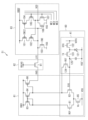
- FIG. 3 is a circuit diagram showing detailed configurations of the differential input circuit 61, the voltage conversion circuit 62, and the positive feedback circuit 63 in the comparison circuit 51 shown in FIG.
- the differential input circuit 61 compares the pixel signal SIG output from the pixel circuit 41 in the pixel 21 and the reference signal REF output from the DAC 25, and when the pixel signal SIG is higher than the reference signal REF, a predetermined Outputs a signal (current).
- the differential input circuit 61 includes transistors 81 and 82 forming a differential pair, transistors 83 and 84 forming a current mirror, a transistor 85 serving as a constant current source that supplies a current IB corresponding to the input bias current Vb, and a differential input circuit 61 . It has a transistor 86 for outputting the output signal HVO of the dynamic input circuit 61 .
- Transistors 81, 82, and 85 are NMOS (Negative Channel MOS) transistors, and transistors 83, 84, and 86 are PMOS (Positive Channel MOS) transistors.
- the gate of the transistor 81 receives the reference signal REF output from the DAC 25
- the gate of the transistor 82 receives the pixel output from the pixel circuit 41 in the pixel 21 .
- a signal SIG is input.
- the sources of transistors 81 and 82 are connected to the drain of transistor 85, and the source of transistor 85 is connected to a predetermined voltage VSS (VSS ⁇ VDD2 ⁇ VDD1).
- the drain of the transistor 81 is connected to the gates of the transistors 83 and 84 and the drain of the transistor 83 that constitute the current mirror circuit, and the drain of the transistor 82 is connected to the drain of the transistor 84 and the gate of the transistor 86 .
- the sources of transistors 83, 84 and 86 are connected to the first power supply voltage VDD1.
- the voltage conversion circuit 62 has an NMOS transistor 91, for example.
- the drain of transistor 91 is connected to the drain of transistor 86 of differential input circuit 61, the source of transistor 91 is connected to a predetermined connection point in positive feedback circuit 63, and the gate of transistor 91 is connected to bias voltage VBIAS. Connected to a node.
- the transistors 81 to 86 forming the differential input circuit 61 are circuits that operate at a high voltage up to the first power supply voltage VDD1, and the positive feedback circuit 63 operates at a second power supply voltage VDD2 lower than the first power supply voltage VDD1.
- the voltage conversion circuit 62 converts the output signal HVO input from the differential input circuit 61 into a low-voltage signal (conversion signal) LVI that allows the positive feedback circuit 63 to operate, and supplies the converted signal to the positive feedback circuit 63 .
- the bias voltage VBIAS may be a voltage that does not destroy the transistors 101 to 105 of the positive feedback circuit 63 operating at a low voltage.
- the positive feedback circuit 63 inverts when the pixel signal SIG is higher than the reference signal REF based on the conversion signal LVI obtained by converting the output signal HVO from the differential input circuit 61 into a signal corresponding to the second power supply voltage VDD2. Output the comparison result signal. Also, the positive feedback circuit 63 speeds up the transition speed when the output signal VCO output as the comparison result signal is inverted.
- the positive feedback circuit 63 has five transistors 101-107.
- transistors 101, 102, 104 and 105 are PMOS transistors and transistors 103, 106 and 107 are NMOS transistors.
- the source of the transistor 91 which is the output terminal of the voltage conversion circuit 62, is connected to the drains of the transistors 102 and 103 and the gates of the transistors 104 and .
- the sources of transistors 101 and 104 are connected to the second power supply voltage VDD2, the drain of transistor 101 is connected to the source of transistor 102, the gate of transistor 102 is connected to transistors 105 and 107 which are also the output of positive feedback circuit 63. connected to the drain of The sources of transistors 103, 106 and 107 are connected to a predetermined voltage VSS.
- the gate of the transistor 101 is supplied with an initialization signal INI2, and the gate of the transistor 103 is supplied with an initialization signal INI.
- any one of a plurality of write enable signals WE1 to WE3, which will be described later, is connected to the gates of the transistors 105 and 107.
- each pixel in the pixel array section 22 belongs to one of a plurality of pixel groups, and has a separate write enable signal for each pixel group.
- the positive feedback circuit 63 of each pixel outputs a valid VCO signal when the corresponding write enable signal is in an enable state (for example, low level). Therefore, when the corresponding write enable signal is not enabled, the positive feedback circuit 63 does not output a valid VCO signal, so the time code corresponding to the pixel data is not stored in the subsequent latch storage section 72.
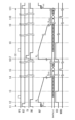
- FIG. 4 is a diagram showing transition of each signal during operation of the comparison circuit 51.
- G86 represents the gate potential of the transistor 86.
- the reference signal REF is set to a voltage higher than the pixel signal SIG of all the pixels 21, the initialization signal INI and the initialization signal INI2 (not shown) are set to high level, and the comparison circuit 51 is initialized. be done.
- the gate of the transistor 81 in FIG. 3 is applied with the reference signal REF, and the gate of the transistor 82 is applied with the pixel signal SIG.
- the voltage of the reference signal REF is higher than the voltage of the pixel signal SIG, most of the current between the drain and source of the transistor 85 serving as a current source flows through the transistor 81 to the diode-connected transistor 83 .
- the channel resistance of transistor 84 which has a gate in common with transistor 83, becomes sufficiently low to keep the gate of transistor 86 substantially at the first power supply voltage VDD1 level, and transistor 86 is cut off. Therefore, even if the transistor 91 of the voltage conversion circuit 62 is conducting, the positive feedback circuit 63 as a charging circuit will not charge the conversion signal LVI.
- the transistor 103 since a high level signal is supplied to the positive feedback circuit 63 as the initialization signal INI, the transistor 103 becomes conductive, and the positive feedback circuit 63 discharges the conversion signal LVI.
- the initialization signal INI2 is at high level and the transistor 101 is cut off, so the positive feedback circuit 63 does not charge the conversion signal LVI through the transistor 102 either.
- the conversion signal LVI is discharged to a predetermined voltage VSS level
- the positive feedback circuit 63 outputs a high-level output signal VCO by the transistors 104 and 106 forming the inverter, and the comparison circuit 51 is initialized. .
- the initialization signals INI and INI2 are both set to low level, the transistor 103 is turned off, and the reference signal REF starts to sweep.
- the transistor 86 is turned off and cut off, and the output signal VCO is a high level signal, so the transistor 102 is also turned off and cut off.
- the transistor 103 is also cut off because the initialization signal INI is at low level.
- the conversion signal LVI maintains a predetermined voltage VSS in a high impedance state, and a high level output signal VCO is output.
- the output current of the current source transistor 85 stops flowing through the transistor 81, the gate potentials of the transistors 83 and 84 rise, and the channel resistance of the transistor 84 increases.
- the current flowing through the transistor 82 causes a voltage drop, lowering the gate potential of the transistor 86, and the transistor 91 becomes conductive.
- the output signal HVO output from the transistor 86 is converted into a conversion signal LVI by the transistor 91 of the voltage conversion circuit 62 and supplied to the positive feedback circuit 63 .
- a positive feedback circuit 63 as a charging circuit charges the converted signal LVI to bring the potential closer to the second power supply voltage VDD2 from the low voltage VSS.
- the output signal VCO becomes low level and the transistor 102 becomes conductive.
- the transistor 101 is also conductive due to the application of the low-level initialization signal INI, and the positive feedback circuit 63 rapidly charges the conversion signal LVI through the transistors 101 and 102, thereby increasing the potential to the second power supply.
- the voltage is raised to VDD2 at once.
- the transistor 91 Since the bias voltage VBIAS is applied to the gate of the transistor 91 of the voltage conversion circuit 62, the transistor 91 is cut off when the voltage of the conversion signal LVI reaches a voltage value that is lower than the bias voltage VBIAS by the threshold value of the transistor. Even though transistor 86 remains conductive, it does not further charge conversion signal LVI, and voltage conversion circuit 62 also functions as a voltage clamp circuit.
- the charging of the conversion signal LVI due to the conduction of the transistor 102 is a positive feedback operation that accelerates the movement, starting from the fact that the conversion signal LVI has risen to the inverter threshold value.
- the transistor 85 which is the current source of the differential input circuit 61, is set to have a very small current per circuit because the number of circuits that operate simultaneously in parallel in the imaging apparatus 1 is enormous.
- the reference signal REF is swept extremely slowly because the voltage that changes in the unit time when the time code is switched is the LSB step of AD conversion. Therefore, the change in the gate potential of the transistor 86 is slow, and the change in the output current of the transistor 86 driven thereby is also slow.
- the output signal VCO can transition sufficiently rapidly.
- the transition time of the output signal VCO is a fraction of the unit time of the time code, typically 1 ns or less.
- the comparison circuit 51 of the present disclosure can achieve this output transition time by setting a small current, for example 0.1 uA, in the transistor 85 of the current source.
- FIG. 5 is a circuit diagram showing the details of the pixel circuit 41 added to the comparison circuit 51 shown in FIG.
- the pixel circuit 41 has a photodiode (PD) 121 as a photoelectric conversion element, an ejection transistor 122, a transfer transistor 123, a reset transistor 124, and an FD (floating diffusion layer) 125.
- a ground node VSS' for the pixel circuit 41 is provided separately from the ground node VSS of the differential input circuit 61 and the positive feedback circuit 63 in the comparison circuit 51.
- FIG. 1 A ground node VSS' for the pixel circuit 41 is provided separately from the ground node VSS of the differential input circuit 61 and the positive feedback circuit 63 in the comparison circuit 51.
- the discharge transistor 122 is used when adjusting the exposure period. Specifically, when the discharge transistor 122 is turned on when the exposure period is to be started at an arbitrary timing, the charge accumulated in the photodiode 121 is discharged, so the discharge transistor 122 is turned off. After that, the exposure period is started.
- the transfer transistor 123 transfers the charges generated by the photodiode 121 to the FD 125 .
- a reset transistor 124 resets the charge held in the FD 125 .
- FD 125 is connected to the gate of transistor 82 of differential input circuit 61 . Thereby, the transistor 82 of the differential input circuit 61 also functions as an amplification transistor of the pixel circuit 41 .
- the source of the reset transistor 124 is connected to the gate of the transistor 82 of the differential input circuit 61 and the FD 125 , and the drain of the reset transistor 124 is connected to the drain of the transistor 82 . Therefore, there is no fixed reset voltage to reset the charge on FD125. This is because the reset voltage for resetting the FD 125 can be arbitrarily set using the reference signal REF by controlling the circuit state of the differential input circuit 61 .
- the reference signal REF is set from the standby voltage Vstb until then to the reset voltage Vrst for resetting the charge of the FD 125, and the reset transistor 124 is turned on, thereby resetting the charge of the FD 125. be done.
- the initialization signal INI supplied to the gates of the transistors 101 and 103 of the positive feedback circuit 63 and the initialization signal INI2 are set to high level, and the positive feedback circuit 63 is set to the initial state. .
- the reference signal REF changes to a predetermined voltage Vu , and comparison between the reference signal REF and the pixel signal SIG (sweep of the reference signal REF) is started.
- the reference signal REF is higher than the pixel signal SIG, so the output signal VCO becomes high level.
- the output signal VCO is inverted (transitioned to low level).
- the positive feedback circuit 63 speeds up the inversion of the output signal VCO as described above.
- the data storage unit 52 also holds time data (N-bit time codes DATA[1] to DATA[N]) at the time when the output signal VCO is inverted.
- the voltage of the reference signal REF supplied to the gate of the transistor 81 of the comparison circuit 51 is at a level at which the transistor 81 turns off (standby voltage V stb ). This suppresses the current consumption of the comparison circuit 51 during the signal read period.
- the WORD signal that controls the read timing goes high, and the held N-bit time codes DATA[1] to DATA[N] are output from the latch control circuit 71 of the data storage unit 52.
- the time code acquired here becomes P-phase data at the reset level when CDS (Correlated Double Sampling) processing is performed.
- the reference signal REF is raised to a predetermined voltage Vu , the initialization signals INI and INI2 supplied to the gates of the transistors 101 and 103 are set to high level, and the positive feedback circuit 63 is again initialized. set.
- the high-level transfer signal TX turns on the transfer transistor 123 of the pixel circuit 41, and the charge accumulated in the photodiode 121 is transferred to the FD125.
- the output signal VCO is inverted (transitioned to low level).
- the positive feedback circuit 63 speeds up the inversion of the output signal VCO.
- the data storage unit 52 holds (stores) time data (N-bit time codes DATA[1] to DATA[N]) at the time when the output signal VCO is inverted.
- the voltage of the reference signal REF supplied to the gate of the transistor 81 of the comparison circuit 51 is at a level at which the transistor 81 turns off (standby voltage V stb ). This suppresses the current consumption of the comparison circuit 51 during the signal read period.
- the WORD signal that controls the read timing becomes high level, and the held (stored) N-bit time codes DATA[1] to DATA[N] are output from the latch control circuit 71 of the data storage unit 52. be.
- the time code acquired here becomes the D-phase data of the signal level at the time of CDS processing.
- Time t11 is the same state as time t1 described above, and the next driving of 1 V (one vertical scanning period) is performed.
- the P-phase data of the reset level is obtained and then read, and then the D-phase data of the signal level is obtained and read.
- each pixel 21 of the pixel array section 22 of the imaging device 1 can perform a global shutter operation in which all pixels are simultaneously reset and all pixels are simultaneously exposed. Since all pixels can be exposed and read out simultaneously, there is no need for a holding section that is normally provided in the pixel to hold charges until the charges are read out. Further, in the configuration of the pixel 21, a selection transistor or the like for selecting a pixel for outputting the pixel signal SIG, which is required in the column-parallel reading type imaging device 1, is not required.
- the discharge transistor 122 was always controlled to be off.
- an arbitrary exposure period can be set by setting the discharge signal OFG to a high level at a desired time to once turn on the discharge transistor 122 and then turn it off. is also possible.
- FIG. 7 is a circuit diagram showing specific configurations of the time code transfer section 23 and the data storage section 52.
- the time code transfer unit 23 has N shift registers 341 - 1 to 341 -N corresponding to N-bit time codes DATA[1] to DATA[N] and a clock supply circuit 342 .
- Each of the N shift registers 341 - 1 to 341 -N consists of a plurality of DF/Fs (D-flip-flops) 351 .
- the clock supply circuit 342 supplies the clock signal CLK to the clock input of each DF/F 351 of the shift register 341 .
- the shift register 341 in the time code transfer unit 23 transfers the number of DF/Fs 351 corresponding to the number of clusters. have.
- the latch control circuit 71 in the data storage unit 52 includes a P-phase latch control unit 241P for P-phase data, a D-phase latch control unit 241D for D-phase data, and N bidirectional buffer circuits 371-1 to 371. -N.
- the latch storage unit 72 in the data storage unit 52 includes P-phase bit storage units 242P-1 to 242P-N for P-phase data and D-phase bit storage units 242D-1 to 242D-N for D-phase data.
- the N bidirectional buffer circuits 371-1 to 371-N are provided in one-to-one correspondence with the N shift registers 341-1 to 341-N of the time code transfer section 23.
- a bidirectional buffer circuit 371 is connected to one DF/F 351 in the corresponding shift register 341 .
- the buffer circuit 381 of the bidirectional buffer circuit 371-N (0 ⁇ n ⁇ N+1) is supplied with a write control signal WR that becomes high in the time code write operation, and the inverter circuit 382 is supplied with the time code read operation. , a read control signal RD of high level is supplied.
- the bi-directional buffer circuit 371-N outputs time codes to the P-phase bit storage units 242P-1 to 242P-N and the D-phase bit storage units 242D-1 to 242D-N based on the write control signal WR and the read control signal RD. switch between write and read operations.
- the data storage unit 52 also has two AND circuits 561P and 561D.
- the output signal VCO output from the comparison circuit 51 is input to one of the two inputs of the AND circuits 561P and 561D.
- the other of the two inputs of the AND circuit 561P receives a P-phase selection signal P_OP that becomes high during the AD conversion period of the P-phase data, and one of the two inputs of the AND circuit 561D receives the AD conversion of the D-phase data.
- a D-phase selection signal D_OP that is at a high level during the period is input.
- Each of the P-phase latch control section 241P and the D-phase latch control section 241D can be configured to have two series-connected inverters 281 and 282, and a series-connected NOR circuit 283 and inverter 284.
- Each of the P-phase bit storage units 242P-1 to 242P-N and the D-phase bit storage units 242D-1 to 242D-N of the data storage unit 52 includes a switch 243 and a latch circuit 244 as shown in FIG. have.
- the switches 243 in the P-phase bit storage units 242P-1 to 242P-N are switch-controlled by the output of the corresponding inverter 284 in the P-phase latch control unit 241P.
- the switches 243 in the D-phase bit storage units 242D-1 to 242D-N are switch-controlled by the output of the corresponding inverter 284 in the D-phase latch control unit 241D.
- the latch circuits 244 in the P-phase bit storage units 242P-1 to 242P-N are output from the bidirectional buffer circuits 371-1 to 371-N according to the outputs of the corresponding inverters 282 in the P-phase latch control unit 241P. Toggles whether to latch the time code.
- the latch circuits 244 in the D-phase bit storage units 242D-1 to 242D-N are output from the bidirectional buffer circuits 371-1 to 371-N according to the outputs of the corresponding inverters 282 in the D-phase latch control unit 241D. Toggles whether to latch the time code.
- the latch circuit 244 may be composed of a semiconductor memory such as an SRAM (Static Random Access Memory) made up of a plurality of transistors.
- each of the P-phase latch control section 241P and the D-phase latch control section 241D needs to have a control circuit configuration that is optimal for the configuration of the employed semiconductor memory. It is preferable that the P-phase latch control section 241P and the D-phase latch control section 241D are combined with a combinational circuit instead of a sequential circuit in order to fit them in a finite area.
- the output signal VCO which is the output from the comparison circuit 51, is input to the inverter 281 and the NOR circuit 283 in each of the P-phase latch control section 241P and the D-phase latch control section 241D.
- a P_WORD signal and a D_WORD signal are provided.
- the output signal of the inverter 281 is inverted by the inverter 282 to control the latch circuits 244 in the P-phase bit storage units 242P-1 to 242P-N and the latches in the D-phase bit storage units 242D-1 to 242D-N. Latch control of circuit 244 is performed.
- the output signal of the NOR circuit 283 is inverted by an inverter 284 to control the switching of the switches 243 in the P-phase bit storage units 242P-1 to 242P-N and the switches in the D-phase bit storage units 242D-1 to 242D-N. H.243 latch control is performed.
- the data storage unit 52 is provided with two AND circuits 561P and 561D.
- the output signal VCO output from the comparison circuit 51 is input to one of the two inputs of the AND circuits 561P and 561D.
- the other of the two inputs of the AND circuit 561P receives a P-phase selection signal P_OP that becomes high during the AD conversion period of the P-phase data, and one of the two inputs of the AND circuit 561D receives the AD conversion of the D-phase data.
- a D-phase selection signal D_OP that is at a high level during the period is input.
- the high-level P-phase selection signal P_OP and the low-level D-phase selection signal D_OP are supplied to the data storage unit 52, and the P-phase bit is supplied to the data storage unit 52.
- P-phase data is stored in storage units 242P-1 to 242P-N.
- the low-level P-phase selection signal P_OP and the high-level D-phase selection signal D_OP are supplied to the data storage section 52, and the D-phase bit storage sections 242D-1 to 242D-N are supplied. D-phase data is stored in . After that, the P-phase data and the D-phase data are output to the time code transfer section 23 in order.
- the time interval between P-phase data acquisition and D-phase data acquisition can be shortened, and the offset and noise cancellation effect of CDS processing can be enhanced. Further, by outputting the P-phase data and the D-phase data to the time code transfer section 23 in order, the memory section for temporarily storing the P-phase data in the output section 28 becomes unnecessary.
- the WORD signal of all pixels becomes low level, and the switch 243 is conductive when the output signal VCO is high level and cuts off when it is low level.
- the feedback of the latch storage unit 72 (output xQ for input Q) is cut off when the output signal VCO is high level and conductive when it is low level. Therefore, when the output signal VCO is at high level, the latch storage unit 72 is in a writing state (transparent) of the n-th bit time code. Then, the written time code is held (latched state).
- a high-level WORD signal is supplied only to the P-phase latch control section 241P and the D-phase latch control section 241D of the pixel 21 to be read. Since the output signal VCO is at the low level, the switch 243 becomes conductive only when the WORD signal at the high level is input, and the time code held in the latch storage section 72 is transferred to the bidirectional buffer circuit 371-N. It is output to the time code transfer section 23 via the time code transfer section 23 .
- the N shift registers 341 of the time code transfer unit 23 transfer the time code supplied from the time code generation unit 26 to the unit time of the time code as the clock cycle. transfer with a shift clock of
- a high-level write control signal WR and a low-level read control signal RD are supplied to the bidirectional buffer circuit 371 .
- the time code supplied from the F/F 351 is stored in the P-phase bit storage units 242P-1 to 202P-N or the D-phase bit storage units 242D-1 to 242D-N.
- the low-level write control signal WR and the high-level read control signal RD are supplied to the bidirectional buffer circuit 371, and the P-phase bit storage units 242P-1 to 202P-N, Alternatively, the time code stored in the D-phase bit storage units 242D-1 to 242D-N is supplied to a predetermined DF/F 351 of the shift register 341 of the time code transfer unit 23 via the bidirectional buffer circuit 371. be.
- the shift register 341 sequentially transfers the time data supplied to the DF/F 351 of each stage to the output unit 28 and outputs the data.
- each DF/F 351 of the shift register 341 is in a high impedance state (hereinafter referred to as a Hi-Z state) while the clock signal CLK supplied to the clock input is either high level or low level. described.) is adopted.
- a Hi-Z state a high impedance state
- the clock signal CLK supplied to the clock input is either high level or low level. described.
- the high level read control signal RD is supplied to the bidirectional buffer circuit 371, and the WORD signal becomes high level to perform bit storage.
- the time code stored in the unit 242 is supplied to a predetermined DF/F 351 of the shift register 341 of the time code transfer unit 23 via the bidirectional buffer circuit 371 .
- a shift clock is supplied to each DF/F 351 of the shift register 341, and the shift register 341 reads the time data supplied to the DF/F 351 of each stage.
- the data is sequentially transferred to the output unit 28 and output.
- FIG. 7 shows an example in which the latch circuits 244 in the P-phase bit storage units 242P-1 to 242P-N and the latch circuits in the D-phase bit storage units 242D-1 to 242D-N are composed of digital memories. , may be composed of an analog memory.
- FIG. 9 is a circuit diagram showing an example in which the latch circuits 244 in the P-phase bit storage units 242P-1 to 242P-N and the latch circuits 244 in the D-phase bit storage units 242D-1 to 242D-N are configured with analog memories.
- FIG. 9 shows a P-phase latch control section 241P and P-phase bit storage sections 242P-1 to 242P-N. Although omitted in FIG. 9, the D-phase latch control section 241D and the D-phase bit storage sections 242D-1 to 242D-N are similarly configured.
- the P-phase bit storage units 242P-1 to 242P-N and 242D-1 to 242D-N in FIG. 9 are composed of analog memories.
- the P-phase bit storage units 242P-1 to 242P-N in FIG. It has a transistor 247 and a transistor 248 connected in series between the ground node.
- Transistors 245, 247, 248 are, for example, NMOS transistors.
- the source of the transistor 245 is connected to the gate of the transistor 248, and the gate of the transistor 245 receives the output signal L of the latch control section 241P.
- FIG. 9 shows a simplified internal configuration of the latch control unit 241P.
- a NAND gate 249 for example, is provided in the latch controller 241P. This NAND gate 249 outputs a high level signal when either the output signal VCO of the positive feedback circuit 63 or the P phase D phase selection signal LATSEL[1:0] is at high level.
- the transistors 245 in the P-phase bit storage sections 242P to 242P-N are turned on, and the capacitors 246 store charges according to the time code.
- transistor 245 is turned off and capacitor 246 holds the accumulated charge. In this state, a voltage corresponding to the charge accumulated in the capacitor 246 is applied to the gate of the transistor 248, but since the second transistor 247 is off, the voltage level of the local bit line LBL does not change.
- the second transistor 247 is turned on, the local bit line LBL becomes the voltage level corresponding to the charge accumulated in the capacitor 246, and the P-phase bit storage units 242P-1 to 242P-N are stored.
- the stored time code is read out to bus 250 via local bit line LBL.
- the imaging device 1 divides a plurality of pixels in the pixel array section 22 into at least two pixel groups, and determines the timing of updating the data stored in the latch storage section 72 in each pixel group. Control.
- the latch control circuit 71 in the data storage unit 52 shown in FIG. is controlled for each pixel group.
- the latch control circuit 71 stores the pixel data in the latch storage unit 72 in the next frame period for those pixel groups for which all the corresponding pixel data cannot be transferred to the output unit 28 within one frame period. is held as it is without being updated, and the transfer to the output unit 28 is continued.
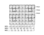
- FIG. 10A is a diagram showing an example of pixel groups in the pixel array section 22.
- FIG. 10A for the sake of simplification, a first pixel group PXG1 indicated by broken lines, a second pixel group PXG2 indicated by thick lines, and It shows an example in which the remaining third pixel group PXG3 indicated by thin lines is provided.
- the number of pixels in the pixel array section 22 and the number of pixel groups provided in the pixel array section 22 are arbitrary.
- the first pixel group PXG1 includes pixel groups of 3 pixels each on the left end and right end in the horizontal direction, and these pixel groups are arranged with an interval of 2 pixels in the vertical direction.
- the second pixel group PXG2 includes a total of four pixels, which are horizontally spaced by four pixels and vertically spaced by two pixels.
- the third pixel group PXG3 includes pixels other than the first pixel group PXG1 and the second pixel group PXG2 in the pixel array section 22 .
- Each pixel in the first pixel group PXG1 is, for example, a pixel for live view (moving image). Since live view does not require resolution as high as that of still images, the first pixel group PXG1 is used, which is made up of some pixels obtained by thinning out the pixels for still images.
- Each pixel in the second pixel group PXG2 is a pixel for image plane phase difference detection.
- Each pixel is divided into two, or half of each pixel is shielded from light, and the phase difference is detected from the optical signal captured in each divided area, and used for, for example, focus adjustment.
- Each pixel in the third pixel group PXG3 is used for capturing a still image, for example.
- a still image is likely to have noticeable image roughness, so it is desirable to have a larger number of pixels than the first pixel group PXG1 and the second pixel group PXG2.
- a first write enable signal WE1 for permitting storage of the pixel signal of each pixel in the first pixel group PXG1 in the latch storage unit 72 and a second write enable signal WE2 that permits storage of the pixel signal of each pixel in the latch storage unit 72; and a third write enable signal WE3.
- One of these first to third write enable signals WE1 to WE3 is connected to the gates of the transistors 105 and 107 of the positive feedback circuit 63 of FIG. 5 for each pixel.
- the types of write enable signals connected to the gates of transistors 105 and 107 in pixels belonging to the same pixel group are the same.
- the pixel data (more precisely, the time code corresponding to the pixel signal) of all the pixels in the first pixel group PXG1 is stored in the corresponding latch storage unit 72. stored in As a result, the pixel data previously stored in the latch storage unit 72 is updated.
- the second write enable signal WE2 is enabled (for example, high level)
- the pixel data of all the pixels in the second pixel group PXG2 are stored in the corresponding latch memory section 72.
- the pixel data previously stored in the latch storage unit 72 is updated.
- the third write enable signal WE3 is enabled (for example, high level)
- the pixel data of all the pixels in the third pixel group PXG3 are stored in the corresponding latch memory section 72.
- the pixel data previously stored in the latch storage unit 72 is updated.
- the pixel data stored in the latch storage unit 72 of each pixel in the first pixel group PXG1, the second pixel group PXG2, and the third pixel group PXG3 can be transferred to the output unit 28 within one frame period.
- the pixel data in the latch storage section 72 of each pixel becomes unnecessary, new pixel data can be stored in the corresponding latch storage section 72 .
- the third pixel group PXG3 there is a possibility that the pixel data of all the pixels cannot be transferred to the output section 28 within one frame period.
- each pixel in the third pixel group PXG3 is output from the latch storage section 72 within one frame period. 28 may not finish transferring pixel data.
- the signal readout time of the pixels in the third pixel group PXG3 is long, there is a possibility that the transfer of all pixel data to the output unit 28 will not be completed within one frame period.
- a write enable signal is individually provided for each pixel group so that whether or not to update the pixel data in the latch storage unit 72 of each pixel can be set for each pixel group.
- control wiring for the first write enable signal WE1, the control wiring for the second write enable signal WE2, and the control wiring for the third write enable signal WE3 are arranged on the pixel that gives write permission, As much as possible, it is arranged so as not to be placed on pixels for which write permission is not given.
- a contact indicated by a black circle on each control line in FIG. 10A indicates a pixel controlled by the corresponding write enable signal.
- Each pixel in the pixel array section 22 is connected to one of the first to third write enable signals WE1 to WE3.
- Arranging the three control wires as shown in FIG. 10A has the advantage of reducing the arrangement area of the control wires and improving the aperture ratio of each pixel.
- the wiring density becomes higher and lower, and the wiring density is not uniform. This may cause variations in pixel characteristics such as variations in sensitivity.
- FIG. 10B is a diagram showing a modified example of FIG. 10A.
- FIG. 10B shows an example of arranging three control lines over all pixels in the pixel array section 22 .
- three control wirings are arranged for all pixels in the pixel array section 22, the arrangement density of the control wirings becomes uniform, and the aperture ratio of each pixel can be made uniform.
- the order of reading the pixel data of each pixel in each pixel group in the pixel array section 22 may be the same or may be different for each pixel group.
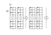
- FIG. 11 is a diagram showing, by arrows, the order of reading pixel data of each pixel in the first pixel group PXG1.
- FIG. 11 shows an example in which the upper left pixel data in each cluster 20 in the first pixel group PXG1 is read and transferred upward.
- the pixel data at the upper left corner in the plurality of clusters 20 transferred by the same time code transfer section 23 are read out and transferred in parallel.
- FIG. 11 shows only the readout order of the pixel data at the upper left corner in each cluster 20, the readout of other pixel data is performed in the same manner.
- FIG. 12 is a diagram showing, by arrows, the readout order of pixel data of the second pixel group PXG2 consisting of a plurality of clusters 20 arranged adjacently in the horizontal and vertical directions.
- FIG. 12 shows an example in which the pixel data of the pixels in the second row from the top in each cluster 20 in the second pixel group PXG2 are read in parallel and transferred upward. Reading other pixel data in each cluster 20 is performed in the same manner as in FIG.
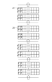
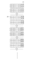
- FIGS. 13A to 13D show an example in which the clusters 20 of the top two rows in the pixel array section 22 are read out first, and then the clusters 20 of the third and subsequent rows are read out. 13A to 13D, pixel data at the same position within each cluster 20 are read out in parallel.
- the pixel data is transferred to the right direction as the time code.
- the pixel data is read out to the time code transfer section 23 in the left direction and then read out to the output section 28. .
- FIGS. 11, 12, and 13A to 13D merely show an example of the order of reading pixel data of the plurality of clusters 20 in the pixel array section 22, and various modifications are conceivable.
- the local bit line LBL may be arranged on both sides from the time code transfer section 23, or may be arranged on one side.
- FIG. 14 is a timing chart of the imaging device 1 according to this embodiment.
- FIG. 14 shows the timing of two frame periods. Each frame is a period from output of the vertical synchronization signal VSYNC to output of the next vertical synchronization signal VSYNC. Time t1 to t10 is the first frame period, and time t11 to t20 is the next frame period.
- FIG. 14 shows an example in which the pixel array section 22 has the first pixel group PXG1, the second pixel group PXG2, and the third pixel group PXG3 shown in FIGS. 10A and 10B.
- the reset transistor 124 shown in FIG. 5 is turned on, and the potential of the FD 125 becomes the reset level. At time t2, the reset transistor 124 is turned off.
- reset level AD conversion is performed for all pixels in the pixel array section 22, and the P-phase pixel data (more precisely, the time code corresponding to the reset level) is converted into FIG. 7 P-phase bit storage units 242P-1 to 242P-N.
- the transfer transistors 123 of all pixels in the pixel array section 22 are turned on, and the charges accumulated in the photodiodes 121 are transferred to the FDs 125 (time t3-t4).
- the photoelectrically converted pixel signals are AD-converted for all the pixels in the pixel array section 22, and D-phase pixel data (more precisely, time code) are stored in the D-phase bit storage units 242D-1 to 242D-N in FIG.
- D-phase pixel data (more precisely, time code) are stored in the D-phase bit storage units 242D-1 to 242D-N in FIG.
- a CDS operation may be performed to obtain the difference between D-phase and P-phase pixel data.
- the latch storage section 72 written under the control of the first write enable signal WE1 is put into the selected state by the corresponding WORD selection control, and belongs to the first pixel group PXG1 in the pixel array section 22.
- Pixel data of each pixel is transferred from the latch storage section 72 to the output section 28 via the time code transfer section 23 .
- the pixel data after CDS is transferred to the output section .
- the CDS operation is not performed within the period from time t4 to t5
- the P-phase and D-phase pixel data are transferred to the output unit 28, and the CDS operation is performed at the output unit 28.
- the latch storage section 72 written under the control of the second write enable signal WE1 is put into the selected state by the corresponding WORD selection control, and belongs to the second pixel group PXG2 in the pixel array section 22. Pixel data of each pixel is transferred from the latch storage section 72 to the output section 28 through the time code transfer section 23 .
- the output unit 28 performs various digital signal processing such as black level correction processing for correcting the black level, and then outputs pixel data to the outside of the imaging device 1 .
- black level correction processing for correcting the black level
- each pixel data in the first pixel group PXG1 is output from the imaging device 1 within the period of time ts1 to t8, and each pixel data in the second pixel group PXG2 is output within the period of time t8 to t9. is output from the imaging device 1 to .
- FIG. 14 shows an example in which transfer of pixel data in the third pixel group PXG3 is not completed by time t10, which is the end of one frame period.
- the next frame period starts from time t11, and during the period from time t11 to t12, similarly to time t1 to t2, the reset transistor 124 is turned on and the potential of the FD 125 becomes the reset level.
- P-phase pixel data (more precisely, the time code corresponding to the reset level) is stored in the P-phase bit storage units 242P-1 to 242P-N in the same manner as at time t2 to t3. .
- the pixel signal accumulated in the photodiode 121 is transferred to the FD 125 as in the time from t3 to t4.
- the D-phase pixel data (more precisely, the time code corresponding to the pixel signal) is stored in the D-phase bit storage units 242D-1 to 242D-N.
- the D-phase bit storage units 242D-1 to 242D-N are not updated, and the pixels stored in the previous frame are not updated. Data is kept as is.
- D-phase pixel data is stored in the D-phase bit storage units 242D-1 to 242D-N only for the pixels belonging to the first pixel group PXG1 and the second pixel group PXG2. remembered.
- the pixel data in the first pixel group PXG1 is transferred to the output unit 28 from time t15 to t16, and the pixel data in the second pixel group PXG2 is transferred to the output unit 28 from time t16 to t17. From time t17 to t20, the pixel data in the third pixel group PXG3 that could not be transferred within the immediately preceding frame period are transferred to the output unit .
- each pixel in the third pixel group PXG3 is latched in the next frame period.
- pixel data can continue to be transferred from latch storage 72 to output 28 during the next frame period.
- the third pixel group PXG3 is for capturing a still image, for example, and it is not necessary to update the pixel data every frame period. Therefore, even if the latch storage unit 72 that stores the pixel data in the third pixel group PXG3 is not updated every frame, no problem occurs in practice.
- the first to third pixel groups PXG1, PGX2, and PXG3 are not necessarily continuous pixel blocks, and pixels adjacent to each pixel in each pixel group belong to another pixel group.
- the spatial resolution of the normal pixel group PXG3 is lowered. Therefore, if a pixel that does not belong to the third pixel group PXG3 exists in the region of the third pixel group PXG3, this pixel is interpolated with the pixel data of the surrounding pixels that belong to the third pixel group PXG3. is desirable.
- Such interpolation processing is performed in the output unit 28, for example.
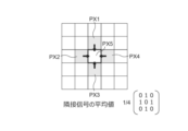
- FIG. 15A, 15B, 15C and 15D are representative specific examples of interpolation processing.
- FIG. 15A shows an example in which a pixel PX5 between four pixels PX1 to PX4 belonging to the third pixel group PXG3 does not belong to the third pixel group PXG3.
- an interpolation process such as averaging the pixel data of the four pixels PX1 is performed to estimate the pixel data of the pixel PX5.
- the lower right of FIG. 15A shows a 3 ⁇ 3 matrix where 1 is the pixel used for interpolation processing. More fine interpolation processing may be performed by increasing the number of rows and columns of the matrix to 4 or more and decreasing the interpolation weight (below 1) as the distance from the pixel to be interpolated increases.
- interpolation processing may be performed using the pixel data of the pixels PX1 to PX4 of the same color arranged one pixel in the horizontal and vertical directions from the pixel PX5 to be interpolated.
- the interpolation processing of FIG. 15B can be represented by a 5 ⁇ 5 matrix as shown in the lower right of FIG. 15B.
- a more detailed interpolation process may be performed by setting a value less than 1 in the places described as 0 in this matrix.
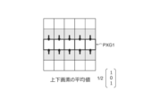
- FIG. 15C shows an example in which, for example, horizontal pixel rows that do not belong to the third pixel group PXG3 are interpolated with pixel rows of the upper and lower third pixel groups PXG3. Interpolation processing is performed using pixel data of two pixels above and below each pixel to be corrected.
- the interpolation processing of FIG. 15C can be represented by a 1 ⁇ 3 matrix as shown in the lower right of FIG. 15C. A more detailed interpolation process may be performed by setting a value less than 1 in the places described as 0 in this matrix.
- FIG. 15D is a modified example of FIG. 15C.
- interpolation may be performed using the pixel data of the pixel rows with the same color above and below.
- the interpolation process of FIG. 15D can be represented by a 1 ⁇ 5 matrix as shown in the lower right of FIG. 15D.
- Interpolation processing can be performed on any of the first to third pixel groups PXG1, PGX2, and PXG3.
- FIG. 16 is a diagram showing an example in which a pixel substrate (first substrate) 12 and a logic substrate (second substrate) 13 are stacked to configure the imaging device 1 .
- the pixel substrate 12 is arranged on the light incident surface side, and the logic substrate 13 is arranged below the pixel substrate 12 .
- the pixel substrate 12 and the logic substrate 13 are bonded by Cu—Cu bonding, vias, bumps, or the like.
- a pixel array section 22 , a pixel bias generation section 14 , a DAC signal connection section 15 , and a pixel drive signal connection section 16 are arranged on the pixel substrate 12 .
- the pixel bias generator 14 generates a bias voltage to be supplied to each pixel in the pixel array section 22 .
- the DAC signal connection section 15 transmits and receives various signals to and from the DAC 25 in the logic board 13 .
- the pixel drive signal connection sections 16 are arranged at both ends of the pixel array section 22 in the horizontal direction, and transmit/receive various signals for AD conversion to/from the logic board 13 .
- a pixel drive circuit 24, a DAC (D/A converter) 25, a time code generation section 26, a vertical drive circuit 27, an output section 28, and a timing generation circuit 29 are formed on the logic board 13.
- the logic board 13 of FIG. 16 shows an example in which the vertical driving circuits 27 are arranged on both sides in the horizontal direction, the vertical driving circuits 27 may be arranged only on one side as shown in FIG.
- the pixel bias generation unit 14 in the pixel substrate 12 and the output unit 28 in the logic substrate 13 transmit and receive various signals by Cu--Cu junction or the like.
- the DAC signal connection portion 15 in the pixel substrate 12 and the DAC 25 in the logic substrate 13 transmit and receive various signals by Cu--Cu bonding or the like. Since the reference signal generated by the DAC 25 is supplied to each pixel on the pixel substrate 12, the wiring for the reference signal on the pixel substrate 12 is arranged in a mesh pattern. In order to shorten the wiring, a plurality of vias are provided in the DAC signal connection portion 15, and the reference signal is supplied to the pixel substrate 12 through the plurality of vias. Further, the pixel driving signal connection portion 16 in the pixel substrate 12 and the pixel driving circuit 24 in the logic substrate 13 transmit and receive various signals by Cu--Cu bonding or the like.
- the DAC signal connection portion 15 in the pixel substrate 12 and the DAC 25 in the logic substrate 13 are arranged at overlapping positions in the stacking direction, but the areas of the DAC signal connection portion 15 and the DAC 25 do not necessarily have to be the same.
- the pixel bias generation unit 14 in the pixel substrate 12 and the output unit 28 in the logic substrate 13 may at least partially overlap in the stacking direction, and the areas of the pixel bias generation unit 14 and the output unit 28 are not necessarily limited to They do not have to be identical.
- the pixel drive signal connection portion 16 in the pixel substrate 12 and the pixel drive circuit 24 in the logic substrate 13 may at least partially overlap in the stacking direction. are not necessarily the same.
- the pixel circuit 41 in the frame 60 in FIG. 5 and part of the differential input circuit 61 in the comparison circuit 51 are arranged on the pixel substrate 12, and the rest is arranged on the logic substrate 13.
- each pixel in the pixel array section 22 may detect various physical quantities such as sound pressure quantity of sound waves and biological information quantity.
- biological information include blood pressure, blood flow, and pulse.
- a plurality of pixel groups provided in the pixel array section 22 may have different pixel characteristics.
- the pixel characteristics may include at least one of pixel sensitivity and a saturation amount capable of accumulating a physical quantity signal.
- the pixel characteristics may include at least one of phase difference, brightness information, gradation information, color information, event information, environment information, biological information, and sound wave information.
- the pixel characteristics may include the resolution of the ADC 42 provided for each pixel in at least two pixel groups.
- the ADC 42 may have different resolutions for each pixel in the first to third pixel groups PXG1, PGX2, and PXG3 in FIG. 10A or 10B. Different resolutions result in different amounts of pixel data.
- the pixel data of the third pixel group PXG3 can be transferred within one frame period. Even if it cannot be completed, according to the present embodiment, pixel data can be continuously transferred within the next frame period, so the resolution of the ADC 42 can be set individually for each pixel group.
- the pixel characteristic may be the storage capacity of the latch storage unit 72 in each pixel.
- the storage capacities of the latch storage units 72 of the pixels of the first to third pixel groups PXG1, PGX2, and PXG3 in FIG. 10A or 10B may be different.
- the resolution of the ADC 42 increases, the amount of pixel data increases, so it is necessary to increase the storage capacity of the latch storage unit 72 as well.
- the exposure time is long, the amount of pixel data increases, so it is necessary to increase the storage capacity of the latch storage unit 72 .
- a plurality of pixel groups provided in the pixel array section 22 may have different signal detection periods.
- the signal detection period may include at least one of exposure time and signal readout time.
- the exposure time of each pixel belonging to the first to third pixel groups PXG1, PGX2, and PXG3 in the pixel array section 22 of FIG. 10A or FIG. The time may be different for each pixel group.
- latch storage for storing AD-converted pixel data is performed for each pixel group. It is possible to control whether or not the section 72 is updated. As a result, for a pixel group whose pixel data cannot be completely transferred to the output unit 28 within one frame period, the latch storage unit 72 is not updated, and pixel data is continuously transferred within the next frame period. It can be performed. Therefore, the pixel characteristics of the plurality of pixel groups in the pixel array section 22 can be made different, and the signal detection periods can be made different, while the pixel data output period can be optimized for each pixel group.
- the technology (the present technology) according to the present disclosure can be applied to various products.
- the technology according to the present disclosure can be realized as a device mounted on any type of moving body such as automobiles, electric vehicles, hybrid electric vehicles, motorcycles, bicycles, personal mobility, airplanes, drones, ships, and robots. may
- FIG. 18 is a block diagram showing a schematic configuration example of a vehicle control system, which is an example of a mobile control system to which the technology according to the present disclosure can be applied.
- a vehicle control system 12000 includes a plurality of electronic control units connected via a communication network 12001.
- the vehicle control system 12000 includes a driving system control unit 12010, a body system control unit 12020, a vehicle exterior information detection unit 12030, a vehicle interior information detection unit 12040, and an integrated control unit 12050.
- a microcomputer 12051, an audio/image output unit 12052, and an in-vehicle network I/F (Interface) 12053 are illustrated as the functional configuration of the integrated control unit 12050.
- the drive system control unit 12010 controls the operation of devices related to the drive system of the vehicle according to various programs.
- the driving system control unit 12010 includes a driving force generator for generating driving force of the vehicle such as an internal combustion engine or a driving motor, a driving force transmission mechanism for transmitting the driving force to the wheels, and a steering angle of the vehicle. It functions as a control device such as a steering mechanism to adjust and a brake device to generate braking force of the vehicle.
- the body system control unit 12020 controls the operation of various devices equipped on the vehicle body according to various programs.
- the body system control unit 12020 functions as a keyless entry system, a smart key system, a power window device, or a control device for various lamps such as headlamps, back lamps, brake lamps, winkers or fog lamps.
- the body system control unit 12020 can receive radio waves transmitted from a portable device that substitutes for a key or signals from various switches.
- the body system control unit 12020 receives the input of these radio waves or signals and controls the door lock device, power window device, lamps, etc. of the vehicle.
- the vehicle exterior information detection unit 12030 detects information outside the vehicle in which the vehicle control system 12000 is installed.
- the vehicle exterior information detection unit 12030 is connected with an imaging section 12031 .
- the vehicle exterior information detection unit 12030 causes the imaging unit 12031 to capture an image of the exterior of the vehicle, and receives the captured image.
- the vehicle exterior information detection unit 12030 may perform object detection processing or distance detection processing such as people, vehicles, obstacles, signs, or characters on the road surface based on the received image.
- the imaging unit 12031 is an optical sensor that receives light and outputs an electrical signal according to the amount of received light.
- the imaging unit 12031 can output the electric signal as an image, and can also output it as distance measurement information.
- the light received by the imaging unit 12031 may be visible light or non-visible light such as infrared rays.
- the in-vehicle information detection unit 12040 detects in-vehicle information.
- the in-vehicle information detection unit 12040 is connected to, for example, a driver state detection section 12041 that detects the state of the driver.
- the driver state detection unit 12041 includes, for example, a camera that captures an image of the driver, and the in-vehicle information detection unit 12040 detects the degree of fatigue or concentration of the driver based on the detection information input from the driver state detection unit 12041. It may be calculated, or it may be determined whether the driver is dozing off.
- the microcomputer 12051 calculates control target values for the driving force generator, the steering mechanism, or the braking device based on information on the inside and outside of the vehicle acquired by the vehicle exterior information detection unit 12030 or the vehicle interior information detection unit 12040, and controls the drive system control unit.
- a control command can be output to 12010 .
- the microcomputer 12051 realizes the functions of ADAS (Advanced Driver Assistance System) including collision avoidance or shock mitigation of vehicles, follow-up driving based on inter-vehicle distance, vehicle speed maintenance driving, vehicle collision warning, vehicle lane deviation warning, etc. Cooperative control can be performed for the purpose of ADAS (Advanced Driver Assistance System) including collision avoidance or shock mitigation of vehicles, follow-up driving based on inter-vehicle distance, vehicle speed maintenance driving, vehicle collision warning, vehicle lane deviation warning, etc. Cooperative control can be performed for the purpose of ADAS (Advanced Driver Assistance System) including collision avoidance or shock mitigation of vehicles, follow-up driving based on inter-vehicle distance, vehicle speed
- the microcomputer 12051 controls the driving force generator, the steering mechanism, the braking device, etc. based on the information about the vehicle surroundings acquired by the vehicle exterior information detection unit 12030 or the vehicle interior information detection unit 12040, so that the driver's Cooperative control can be performed for the purpose of autonomous driving, etc., in which vehicles autonomously travel without depending on operation.
- the microcomputer 12051 can output a control command to the body system control unit 12030 based on the information outside the vehicle acquired by the information detection unit 12030 outside the vehicle.
- the microcomputer 12051 controls the headlamps according to the position of the preceding vehicle or the oncoming vehicle detected by the vehicle exterior information detection unit 12030, and performs cooperative control aimed at anti-glare such as switching from high beam to low beam. It can be carried out.
- the audio/image output unit 12052 transmits at least one of audio and/or image output signals to an output device capable of visually or audibly notifying the passengers of the vehicle or the outside of the vehicle.
- an audio speaker 12061, a display unit 12062, and an instrument panel 12063 are illustrated as output devices.
- the display unit 12062 may include at least one of an on-board display and a head-up display, for example.
- FIG. 19 is a diagram showing an example of the installation position of the imaging unit 12031.
- the imaging unit 12031 has imaging units 12101, 12102, 12103, 12104, and 12105.
- the imaging units 12101, 12102, 12103, 12104, and 12105 are provided at positions such as the front nose, side mirrors, rear bumper, back door, and windshield of the vehicle 12100, for example.
- An image pickup unit 12101 provided in the front nose and an image pickup unit 12105 provided above the windshield in the passenger compartment mainly acquire images in front of the vehicle 12100 .
- Imaging units 12102 and 12103 provided in the side mirrors mainly acquire side images of the vehicle 12100 .
- An imaging unit 12104 provided in the rear bumper or back door mainly acquires an image behind the vehicle 12100 .
- the imaging unit 12105 provided above the windshield in the passenger compartment is mainly used for detecting preceding vehicles, pedestrians, obstacles, traffic lights, traffic signs, lanes, and the like.
- FIG. 19 shows an example of the imaging range of the imaging units 12101 to 12104.
- the imaging range 12111 indicates the imaging range of the imaging unit 12101 provided in the front nose
- the imaging ranges 12112 and 12113 indicate the imaging ranges of the imaging units 12102 and 12103 provided in the side mirrors, respectively
- the imaging range 12114 The imaging range of an imaging unit 12104 provided on the rear bumper or back door is shown. For example, by superimposing the image data captured by the imaging units 12101 to 12104, a bird's-eye view image of the vehicle 12100 viewed from above can be obtained.
- At least one of the imaging units 12101 to 12104 may have a function of acquiring distance information.
- at least one of the imaging units 12101 to 12104 may be a stereo camera composed of a plurality of imaging elements, or may be an imaging element having pixels for phase difference detection.
- the microcomputer 12051 determines the distance to each three-dimensional object within the imaging ranges 12111 to 12114 and changes in this distance over time (relative velocity with respect to the vehicle 12100). , it is possible to extract, as the preceding vehicle, the closest three-dimensional object on the traveling path of the vehicle 12100, which runs at a predetermined speed (for example, 0 km/h or more) in substantially the same direction as the vehicle 12100. can. Furthermore, the microcomputer 12051 can set the inter-vehicle distance to be secured in advance in front of the preceding vehicle, and perform automatic brake control (including following stop control) and automatic acceleration control (including following start control). In this way, cooperative control can be performed for the purpose of automatic driving in which the vehicle runs autonomously without relying on the operation of the driver.
- automatic brake control including following stop control
- automatic acceleration control including following start control
- the microcomputer 12051 converts three-dimensional object data related to three-dimensional objects to other three-dimensional objects such as motorcycles, ordinary vehicles, large vehicles, pedestrians, and utility poles. It can be classified and extracted and used for automatic avoidance of obstacles. For example, the microcomputer 12051 distinguishes obstacles around the vehicle 12100 into those that are visible to the driver of the vehicle 12100 and those that are difficult to see. Then, the microcomputer 12051 judges the collision risk indicating the degree of danger of collision with each obstacle, and when the collision risk is equal to or higher than the set value and there is a possibility of collision, the obstacle is detected through the audio speaker 12061 and the display unit 12062. By outputting an alarm to the driver via the drive system control unit 12010 and performing forced deceleration and avoidance steering via the drive system control unit 12010, driving support for collision avoidance can be performed.
- At least one of the imaging units 12101 to 12104 may be an infrared camera that detects infrared rays.
- the microcomputer 12051 can recognize a pedestrian by determining whether or not the pedestrian exists in the captured images of the imaging units 12101 to 12104 .
- recognition of a pedestrian is performed by, for example, a procedure for extracting feature points in images captured by the imaging units 12101 to 12104 as infrared cameras, and performing pattern matching processing on a series of feature points indicating the outline of an object to determine whether or not the pedestrian is a pedestrian.
- the audio image output unit 12052 outputs a rectangular outline for emphasis to the recognized pedestrian. is superimposed on the display unit 12062 . Also, the audio/image output unit 12052 may control the display unit 12062 to display an icon or the like indicating a pedestrian at a desired position.
- the technology according to the present disclosure can be applied to the imaging unit 12031 and the like among the configurations described above.
- the solid-state imaging device 1 of the present disclosure can be applied to the imaging unit 12031 .
- this technique can take the following structures. (1) at least two groups of pixels each detecting a physical quantity; a storage unit that stores data corresponding to physical quantities detected by individual pixels in the pixel group; A physical quantity detection device, comprising: a storage control unit that controls storage of the data in the storage unit and controls whether or not to update the data stored in the storage unit for each pixel group. (2) The physical quantity detection device according to (1), wherein the storage unit is an analog memory or a digital memory. (3) an AD converter that has the storage unit and converts the physical quantity signal into a digital signal by comparing the physical quantity signal detected for each pixel in the pixel group with a reference signal; The physical quantity detection device according to (1) or (2).
- the physical quantity detection device (4) a time code generator that generates a time code that changes with time; a reference signal generator that generates the reference signal whose voltage level changes with time;
- the physical quantity detection device wherein the storage unit stores the time code according to timing at which the time code and the reference signal match.
- all pixels in the two pixel groups detect the physical quantity at the same timing every predetermined period;
- the storage control unit stores, among the at least two pixel groups, pixel groups in which data in the storage unit of all corresponding pixels within the predetermined period cannot be output in the storage unit during the next predetermined period.
- the physical quantity detection device according to any one of (1) to (4), which holds the obtained data without updating.
- the physical quantity detection device (6) The physical quantity detection device according to (5), wherein the predetermined period is a period of a vertical synchronization signal. (7) The physical quantity detection device according to any one of (1) to (6), wherein the at least two pixel groups have different pixel characteristics. (8) The physical quantity detection device according to (7), wherein the pixel characteristics include at least one of pixel sensitivity and a saturation amount capable of accumulating a physical quantity signal. (9) The physical quantity detection device according to (7), wherein the pixel characteristics include at least one of phase difference, luminance information, gradation information, color information, event information, environment information, biological information, and sound wave information.
- the physical quantity detection device (10) The physical quantity detection device according to (7), wherein the pixel characteristics include resolution of an AD converter provided for each pixel in the at least two pixel groups. (11) The physical quantity detection device according to (7), wherein the pixel characteristics include the storage capacity of the storage unit. (12) The physical quantity detection device according to any one of (1) to (11), wherein the at least two pixel groups have different signal detection periods. (13) The physical quantity detection device according to (12), wherein the signal detection period includes at least one of exposure time and signal readout time. (14) Any one of (1) to (13), comprising an interpolation processing unit that interpolates the physical quantity of a pixel not included in the pixel group with the physical quantity of the pixel in the pixel group located around the pixel. 1.
- the physical quantity detection device according to item 1.
- a pixel array section having a plurality of pixels divided into the at least two pixel groups; a plurality of control wirings for controlling readout of all pixels in the pixel array section;
- the plurality of control wirings are arranged in a region of all pixels in the pixel array section;
- the physical quantity detection device according to (15), wherein each pixel in the pixel array section is connected to one of the plurality of control wirings via the contact.
- the physical quantity detection device according to any one of (1) to (16), wherein the physical quantity includes at least one of light intensity, sound pressure of sound waves, and amount of biological information. (18) the physical quantity includes light intensity; Any one of (1) to (17), wherein the at least two pixel groups include at least one of a region for capturing a still image, a region for capturing a moving image, and a region for detecting an image plane phase difference. 1. The physical quantity detection device according to item 1.
- a pixel array section having a plurality of pixels, the plurality of pixels being divided into at least two pixel groups; an AD converter provided for each pixel for analog-to-digital conversion of pixel signals; a time code generator that generates a time code that changes with time; a reference signal generator that generates a reference signal whose voltage level changes over time; a signal processing unit that performs signal processing on pixel data output from the AD converter for each pixel,
- the AD converter has a storage unit that stores the time code corresponding to the pixel signal by comparing the pixel signal with the reference signal,
- the imaging apparatus further comprising a storage control unit that controls storage of the time code in the storage unit and controls whether or not the time code stored in the storage unit is updated for each pixel group.
- the storage control section stores the corresponding time data in the storage section within the next vertical synchronization period.
- Imaging device 11
- Semiconductor substrate 12
- Pixel substrate 13
- Pixel bias generator 15
- DAC signal connection 16
- Pixel drive signal connection 20
- Cluster 21 Pixel 22
- Pixel array 23
- Time code transfer section 24
- pixel drive circuit 26
- time code generation section 27
- vertical drive circuit 28
- 29 timing generation circuit 41
- pixel circuit, 42 AD converter
- 51 comparison circuit 52
- data storage section 60 frame, 61 difference dynamic input circuit, 62 voltage conversion circuit, 63 positive feedback circuit
- 71 latch control circuit 72 latch storage section, 121 photodiode, 122 discharge transistor, 123 transfer transistor, 124 reset transistor, 202 P-N P phase bit storage section, 241D D-phase latch control unit, 241D latch control unit, 241P P-phase latch control unit, 241P latch control unit, 242 bit storage unit, 242D-1 D-phase bit storage unit, 242D-N D-phase bit storage unit, 242P P-phase bit Storage unit, 242P-1 P-phase bit storage unit, 242
Landscapes
- Engineering & Computer Science (AREA)
- Multimedia (AREA)
- Signal Processing (AREA)
- Transforming Light Signals Into Electric Signals (AREA)
Abstract
[課題]画素データの転送が間に合わないという不具合を防止する。 [解決手段]物理量検出装置は、それぞれが物理量を検出する少なくとも2つの画素群と、個々の前記画素群内の画素で検出された物理量に応じたデータを記憶する記憶部と、前記記憶部に前記データを記憶する制御を行うとともに、前記記憶部に記憶された前記データを更新するか否かを前記画素群ごとに制御する記憶制御部と、を備える。
Description
本開示は、物理量検出装置及び撮像装置に関する。
画素ごとに光電変換された画素信号を、画素ごとにアナログ-デジタル変換(以下、AD変換)を行うAD変換器(以下、ADC)を有する画素ADC方式の撮像装置が知られている(特許文献1参照)。画素ADC方式の撮像装置では、画素ごとに、ADCと、AD変換された画素データを記憶する記憶部とを設けるのが一般的である。
画素ADC方式の撮像装置では、各画素でAD変換された画素データを出力部に転送する。画素データの転送は、垂直同期期間内、すなわち1フレーム期間内に行う必要がある。しかしながら、画素数が多くなったり、フレームレートが高速化すると、AD変換された画素データを1フレーム期間内に出力部に転送しきれなくなり、撮像画像の画質が低下するなどの不具合が生じるおそれがある。
最近では、画素アレイ部内の各画素を、撮像目的以外(例えば、種々の物理量の検出など)にも用いる場合がある。また、撮像目的であっても、動画撮像と静止画撮像では、必要とされるフレームレートや解像度が異なる。1フレーム期間に画像データの転送が間に合わなくなると、物理量を正常に検出できない等の不具合が生じる。
そこで、本開示では、画素データの転送が間に合わないという不具合を防止可能な物理量検出装置及び撮像装置を提供するものである。
上記の課題を解決するために、本開示によれば、それぞれが物理量を検出する少なくとも2つの画素群と、
個々の前記画素群内の画素で検出された物理量に応じたデータを記憶する記憶部と、
前記記憶部に前記データを記憶する制御を行うとともに、前記記憶部に記憶された前記データを更新するか否かを前記画素群ごとに制御する記憶制御部と、を備える、物理量検出装置が提供される。
個々の前記画素群内の画素で検出された物理量に応じたデータを記憶する記憶部と、
前記記憶部に前記データを記憶する制御を行うとともに、前記記憶部に記憶された前記データを更新するか否かを前記画素群ごとに制御する記憶制御部と、を備える、物理量検出装置が提供される。
前記記憶部は、アナログメモリ又はデジタルメモリであってもよい。
前記記憶部を有し、個々の前記画素群内の画素ごとに検出された物理量信号と参照信号とを比較することにより、前記物理量信号をデジタル信号に変換するAD変換器を備えてもよい。
時間とともに変化する時刻コードを生成する時刻コード発生部と、
時間とともに電圧レベルが変化する前記参照信号を生成する参照信号生成部と、を備え、
前記記憶部は、前記時刻コードと前記参照信号とが一致するタイミングに応じた前記時刻コードを記憶してもよい。
時間とともに電圧レベルが変化する前記参照信号を生成する参照信号生成部と、を備え、
前記記憶部は、前記時刻コードと前記参照信号とが一致するタイミングに応じた前記時刻コードを記憶してもよい。
前記2つの画素群内の全画素は、所定の期間ごとに同じタイミングで前記物理量を検出し、
前記記憶制御部は、前記少なくとも2つの画素群のうち、前記所定の期間内に対応する全画素の前記記憶部内のデータを出力できない画素群については、次の所定の期間に前記記憶部に記憶されたデータを更新せずに保持してもよい。
前記記憶制御部は、前記少なくとも2つの画素群のうち、前記所定の期間内に対応する全画素の前記記憶部内のデータを出力できない画素群については、次の所定の期間に前記記憶部に記憶されたデータを更新せずに保持してもよい。
前記所定の期間は、垂直同期信号の周期であってもよい。
前記少なくとも2つの画素群は、それぞれ異なる画素特性を有してもよい。
前記画素特性は、画素の感度と、物理量信号を蓄積可能な飽和量との少なくとも一方を含んでもよい。
前記画素特性は、位相差、輝度情報、階調情報、色情報、イベント情報、環境情報、生体情報、及び音波情報の少なくとも一つを含んでもよい。
前記画素特性は、前記少なくとも2つの画素群内の画素ごとに設けられるAD変換器の分解能を含んでもよい。
前記画素特性は、前記記憶部の記憶容量を含んでもよい。
前記少なくとも2つの画素群は、それぞれ異なる信号検出期間を有してもよい。
前記信号検出期間は、露光時間及び信号読出し時間の少なくとも一方を含んでもよい。
前記画素群に含まれない画素の物理量を、当該画素の周囲に位置する前記画素群内の画素の物理量にて補間する補間処理部を備えてもよい。
前記少なくとも2つの画素群に分けられる複数の画素を有する画素アレイ部と、
前記画素アレイ部内の全画素の読み出しを制御する複数の制御配線と、
前記画素アレイ部内の各画素が属する前記画素群に合わせて、各画素と対応する制御配線とを接続するコンタクトと、を備えてもよい。
前記画素アレイ部内の全画素の読み出しを制御する複数の制御配線と、
前記画素アレイ部内の各画素が属する前記画素群に合わせて、各画素と対応する制御配線とを接続するコンタクトと、を備えてもよい。
前記複数の制御配線は、前記画素アレイ部内の全画素の領域に配置され、
前記画素アレイ部内の各画素は、前記複数の制御配線のうちいずれか一つに前記コンタクトを介して接続されてもよい。
前記画素アレイ部内の各画素は、前記複数の制御配線のうちいずれか一つに前記コンタクトを介して接続されてもよい。
前記物理量は、光強度、音波の音圧、及び生体情報量の少なくとも一つを含んでもよい。
前記物理量は、光強度を含み、
前記少なくとも2つの画素群は、静止画画像を撮像する領域と、動画を撮像する領域と、像面位相差を検出する領域との少なくとも一つを含んでもよい。
前記少なくとも2つの画素群は、静止画画像を撮像する領域と、動画を撮像する領域と、像面位相差を検出する領域との少なくとも一つを含んでもよい。
本開示によれば、複数の画素を有し、前記複数の画素が少なくとも2つの画素群に分けられる画素アレイ部と、
画素ごとに設けられ、画素信号をアナログ-デジタル変換するAD変換器と、
時間とともに変化する時刻コードを生成する時刻コード発生部と、
時間とともに電圧レベルが変化する参照信号を生成する参照信号生成部と、
画素ごとの前記AD変換器から出力された画素データに対して信号処理を行う信号処理部と、を備え、
前記AD変換器は、前記画素信号を前記参照信号と比較することにより、前記画素信号に応じた前記時刻コードを記憶する記憶部を有し、
前記記憶部に前記時刻コードを記憶する制御を行うとともに、前記記憶部に記憶された前記時刻コードを更新するか否かを前記画素群ごとに制御する記憶制御部をさらに備える、撮像装置が提供される。
画素ごとに設けられ、画素信号をアナログ-デジタル変換するAD変換器と、
時間とともに変化する時刻コードを生成する時刻コード発生部と、
時間とともに電圧レベルが変化する参照信号を生成する参照信号生成部と、
画素ごとの前記AD変換器から出力された画素データに対して信号処理を行う信号処理部と、を備え、
前記AD変換器は、前記画素信号を前記参照信号と比較することにより、前記画素信号に応じた前記時刻コードを記憶する記憶部を有し、
前記記憶部に前記時刻コードを記憶する制御を行うとともに、前記記憶部に記憶された前記時刻コードを更新するか否かを前記画素群ごとに制御する記憶制御部をさらに備える、撮像装置が提供される。
前記記憶制御部は、垂直同期期間内に全画素の画素データを前記信号処理部に転送できなかった画素群については、次の垂直同期期間内に、対応する前記記憶部内の前記時刻コードを更新せずに保持してもよい。
以下、図面を参照して、物理量検出装置及び撮像装置の実施形態について説明する。以下では、物理量検出装置及び撮像装置の主要な構成部分を中心に説明するが、物理量検出装置及び撮像装置には、図示又は説明されていない構成部分や機能が存在しうる。以下の説明は、図示又は説明されていない構成部分や機能を除外するものではない。
以下では、物理量検出装置の一例として、撮像装置について主に説明するが、後述するように、本開示の物理量検出装置は必ずしも撮像装置に限定されるものではない。
<撮像装置の概略構成例>
図1は、本開示に係る撮像装置1の概略構成を示している。以下では、半導体基板上に形成される撮像装置1を主に説明する。この種の撮像装置1は固体撮像装置1とも呼ばれるが、以下では単に撮像装置1と呼ぶ。
図1は、本開示に係る撮像装置1の概略構成を示している。以下では、半導体基板上に形成される撮像装置1を主に説明する。この種の撮像装置1は固体撮像装置1とも呼ばれるが、以下では単に撮像装置1と呼ぶ。
図1の撮像装置1は、半導体として例えばシリコン(Si)を用いた半導体基板11に、画素21が2次元アレイ状に配列された画素アレイ部22を有する。画素アレイ部22には、時刻コード発生部26で生成された時刻コードを各画素21に転送する時刻コード転送部23が設けられている。そして、半導体基板11上の画素アレイ部22の周辺には、画素駆動回路24、DAC(D/A Converter、参照信号生成部)25、時刻コード発生部26、垂直駆動回路27、出力部28、及びタイミング生成回路29が形成されている。
図2は画素アレイ部22内の2次元アレイ状に配列された各画素21の構成を示すブロック図である。各画素21は、図2に示すように、画素回路41とADC42を有する。各画素21は、画素内の受光素子(例えば、フォトダイオード)で受光した光量に応じた電荷信号を生成し、デジタルの画素信号に変換して出力する。
図1の画素駆動回路24は、画素21内の画素回路41(図2)を駆動する。DAC25は、時間経過に応じてレベル(電圧)が単調減少するスロープ信号である参照信号(基準電圧信号)REFを生成し、各画素21に供給する。時刻コード発生部26は、各画素21が、アナログの画素信号SIGをデジタルの画素信号に変換(AD変換)する際に使用される時刻コードを生成し、対応する時刻コード転送部23に供給する。画素アレイ部22には、複数の時刻コード発生部26が設けられており、画素アレイ部22内には、時刻コード発生部26に対応する数だけ、時刻コード転送部23が設けられている。即ち、時刻コード発生部26と、そこで生成された時刻コードを転送する時刻コード転送部23は、1対1に対応する。
垂直駆動回路27は、画素21内で生成されたデジタルの画素信号を、タイミング生成回路29から供給されるタイミング信号に基づいて、所定の順番で時刻コード転送部23を通じて出力部28に出力させる制御を行う。画素21から出力されたデジタルの画素信号は、出力部28から撮像装置1の外部へ出力される。出力部28は、黒レベルを補正する黒レベル補正処理やCDS(Correlated Double Sampling;相関2重サンプリング)処理など、所定のデジタル信号処理を必要に応じて行い、その後、外部へ出力する。このように、出力部28は、各種の演算処理や信号処理を行う機能を内蔵している。
タイミング生成回路29は、各種のタイミング信号を生成するタイミングジェネレータなどを有し、生成した各種のタイミング信号を、画素駆動回路24、DAC25、垂直駆動回路27等に供給する。
撮像装置1は、上述した構成を備えている。なお、図1では、上述したように、撮像装置1を構成する全ての回路が、1つの半導体基板11上に形成されるように説明したが、後述するように、撮像装置1を構成する回路を複数枚の半導体基板11に分けて配置する構成とすることもできる。
<画素の詳細構成例>
図2に示すように、画素21は、画素回路41とADC(AD変換器)42とを有する。このように、本実施形態による撮像装置1は、各画素がADC42を有する画素ADC方式の撮像装置1である。
図2に示すように、画素21は、画素回路41とADC(AD変換器)42とを有する。このように、本実施形態による撮像装置1は、各画素がADC42を有する画素ADC方式の撮像装置1である。
画素回路41は、受光した光量に応じた電荷信号をアナログの画素信号SIGとしてADC42に出力する。ADC42は、画素回路41から供給されたアナログの画素信号SIGをデジタルの画素信号に変換する。ADC42は、比較回路51とデータ記憶部52とを有する。
比較回路51は、DAC25から供給される参照信号REFと画素信号SIGを比較し、比較結果を表す比較結果信号として、出力信号VCOを出力する。比較回路51は、参照信号REFと画素信号SIGが同一(の電圧)になったとき、出力信号VCOの電位を反転させる。
比較回路51は、差動入力回路61、電圧変換回路62、及び正帰還回路(PFB:positive feedback)63を有する。比較回路51の詳細な構成は、図3を参照して後述する。
データ記憶部52には、比較回路51から出力信号VCOが入力される他、垂直駆動回路27から、画素信号の書き込み動作であることを表すWR信号(以下では、書き込み制御信号WRともいう)、画素信号の読み出し動作であることを表すRD信号(以下では、読み出し制御信号RDともいう)、及び、画素信号の読み出し動作中における画素21の読み出しタイミングを制御するWORD信号が、垂直駆動回路27から供給される。また、データ記憶部52には、時刻コード転送部23を介して、時刻コード発生部26で生成された時刻コードも供給される。
データ記憶部52は、WR信号及びRD信号に基づいて、時刻コードの書き込み動作と読み出し動作を制御するラッチ制御回路(記憶制御部)71と、時刻コードを記憶するラッチ記憶部72とを有する。
ラッチ制御回路71は、時刻コードの書き込み動作においては、比較回路51からハイレベルの出力信号VCOが入力されている間、時刻コード転送部23から供給される、単位時間ごとに更新される時刻コードをラッチ記憶部72に記憶させる。そして、参照信号REFと画素信号SIGが同一(の電圧)になり、比較回路51から供給される出力信号VCOがローレベルに反転されたとき、供給される時刻コードの書き込み(更新)を中止し、最後にラッチ記憶部72に記憶された時刻コードをラッチ記憶部72に保持させる。ラッチ記憶部72に保持された時刻コードは、画素信号SIGと参照信号REFが等しくなった時刻を表しており、画素信号SIGがその時刻の基準電圧であったことを示すデータ、即ち、デジタル化された光量値を表す。
参照信号REFの掃引が終了し、画素アレイ部22内の全ての画素21のラッチ記憶部72に時刻コードが保持された後、画素21の動作が、書き込み動作から読み出し動作に変更される。
ラッチ制御回路71は、時刻コードの読み出し動作においては、読出し制御信号RDと読み出しタイミングを制御するWORD信号に基づいて、画素21が自分の読み出しタイミングとなったときに、ラッチ記憶部72に記憶されている時刻コード(デジタルの画素信号)を、時刻コード転送部23に出力する。時刻コード転送部23は、供給された時刻コードを、読出し方向(図1の出力部28に向かう列方向(垂直方向))に順次転送し、出力部28に供給する。時刻コード転送部23は、隣接して配置された複数の画素を含むクラスタを単位として、時刻コードを転送する場合もある。
<比較回路の構成例>
図3は、図2に示す比較回路51内の差動入力回路61、電圧変換回路62、及び正帰還回路63の詳細構成を示す回路図である。
図3は、図2に示す比較回路51内の差動入力回路61、電圧変換回路62、及び正帰還回路63の詳細構成を示す回路図である。
差動入力回路61は、画素21内の画素回路41から出力された画素信号SIGと、DAC25から出力された参照信号REFとを比較し、画素信号SIGが参照信号REFよりも高いときに所定の信号(電流)を出力する。
差動入力回路61は、差動対となるトランジスタ81及び82、カレントミラーを構成するトランジスタ83及び84、入力バイアス電流Vbに応じた電流IBを供給する定電流源としてのトランジスタ85、並びに、差動入力回路61の出力信号HVOを出力するトランジスタ86を有する。
トランジスタ81、82、及び85は、NMOS(Negative Channel MOS)トランジスタであり、トランジスタ83、84、及び86は、PMOS(Positive Channel MOS)トランジスタである。
差動対となるトランジスタ81及び82のうち、トランジスタ81のゲートには、DAC25から出力された参照信号REFが入力され、トランジスタ82のゲートには、画素21内の画素回路41から出力された画素信号SIGが入力される。トランジスタ81と82のソースは、トランジスタ85のドレインと接続され、トランジスタ85のソースは、所定の電圧VSS(VSS<VDD2<VDD1)に接続されている。
トランジスタ81のドレインは、カレントミラー回路を構成するトランジスタ83及び84のゲート及びトランジスタ83のドレインと接続され、トランジスタ82のドレインは、トランジスタ84のドレイン及びトランジスタ86のゲートと接続されている。トランジスタ83、84、及び86のソースは、第1電源電圧VDD1に接続されている。
電圧変換回路62は、例えば、NMOS型のトランジスタ91を有する。トランジスタ91のドレインは、差動入力回路61のトランジスタ86のドレインと接続され、トランジスタ91のソースは、正帰還回路63内の所定の接続点に接続され、トランジスタ91のゲートは、バイアス電圧VBIASのノードに接続されている。
差動入力回路61を構成するトランジスタ81~86は、第1電源電圧VDD1までの高電圧で動作する回路であり、正帰還回路63は、第1電源電圧VDD1よりも低い第2電源電圧VDD2で動作する回路である。電圧変換回路62は、差動入力回路61から入力される出力信号HVOを、正帰還回路63が動作可能な低電圧の信号(変換信号)LVIに変換して、正帰還回路63に供給する。
バイアス電圧VBIASは、低電圧で動作する正帰還回路63の各トランジスタ101~105を破壊しない電圧に変換する電圧であれば良い。例えば、バイアス電圧VBIASは、正帰還回路63の第2電源電圧VDD2と同じ電圧(VBIAS=VDD2)とすることができ、VBIAS=VDD2としても同様の電圧変換効果を得られる
正帰還回路63は、差動入力回路61からの出力信号HVOを第2電源電圧VDD2に対応する信号に変換した変換信号LVIに基づいて、画素信号SIGが参照信号REFよりも高いときに反転する比較結果信号を出力する。また、正帰還回路63は、比較結果信号として出力する出力信号VCOが反転するときの遷移速度を高速化する。
正帰還回路63は、5つのトランジスタ101~107を有する。ここで、トランジスタ101、102、104、及び105は、PMOSトランジスタであり、トランジスタ103、106、及び107は、NMOSトランジスタである。
電圧変換回路62の出力端であるトランジスタ91のソースは、トランジスタ102及び103のドレインと、トランジスタ104及び106のゲートに接続されている。トランジスタ101及び104のソースは、第2電源電圧VDD2に接続され、トランジスタ101のドレインは、トランジスタ102のソースと接続され、トランジスタ102のゲートは、正帰還回路63の出力端でもあるトランジスタ105及び107のドレインと接続されている。トランジスタ103、106、及び107のソースは、所定の電圧VSSに接続されている。トランジスタ101のゲートには初期化信号INI2が供給され、トランジスタ103のゲートには初期化信号INIが供給される。
トランジスタ105及び107のゲートには、後述する複数のライトイネーブル信号WE1~WE3のいずれか一つが接続されている。後述するように、画素アレイ部22内の各画素は、複数の画素群のいずれかに属しており、画素群ごとに別個にライトイネーブル信号を有する。各画素の正帰還回路63は、対応するライトイネーブル信号がイネーブル状態(例えばローレベル)のときに、有効なVCO信号を出力する。よって、対応するライトイネーブル信号がイネーブル状態でない場合は、正帰還回路63からは有効なVCO信号が出力されないため、後段のラッチ記憶部72に画素データに対応する時刻コードが記憶されない。
以上のように構成される比較回路51の動作について説明する。図4は、比較回路51の動作中の各信号の遷移を表す図である。なお、図4において“G86”はトランジスタ86のゲート電位を表している。
まず、参照信号REFが、全ての画素21の画素信号SIGよりも高い電圧に設定されるとともに、初期化信号INIおよび,図示しない初期化信号INI2がハイレベルにされて、比較回路51が初期化される。
より具体的には、図3のトランジスタ81のゲートには参照信号REFが、トランジスタ82のゲートには画素信号SIGが印加される。参照信号REFの電圧が、画素信号SIGの電圧よりも高い電圧の時は電流源となるトランジスタ85のドレイン-ソース間の電流のほとんどがトランジスタ81を経由してダイオード接続されたトランジスタ83に流れる。トランジスタ83と共通のゲートを持つトランジスタ84のチャネル抵抗は十分低くなり、トランジスタ86のゲートをほぼ第1電源電圧VDD1レベルに保ち、トランジスタ86は遮断される。したがって、電圧変換回路62のトランジスタ91が導通していたとしても、充電回路としての正帰還回路63が変換信号LVIを充電することは無い。一方、正帰還回路63には、初期化信号INIとしてハイレベルの信号が供給されることから、トランジスタ103は導通し、正帰還回路63は変換信号LVIを放電する。このとき、初期化信号INI2はハイレベルであり、トランジスタ101は遮断するので、正帰還回路63がトランジスタ102を介して変換信号LVIを充電することもない。その結果、変換信号LVIは、所定の電圧VSSレベルまで放電され、正帰還回路63は、インバータを構成するトランジスタ104と106によってハイレベルの出力信号VCOを出力し、比較回路51が初期化される。初期化の後、初期化信号INI、INI2はともにローレベルにされて、トランジスタ103はオフし、参照信号REFの掃引が開始される。
参照信号REFが画素信号SIGよりも高い電圧の期間では、トランジスタ86はオフとなるため遮断され、出力信号VCOはハイレベルの信号となるので、トランジスタ102もオフとなり遮断される。トランジスタ103も、初期化信号INIはローレベルとなっているため遮断される。変換信号LVIは、高インピーダンス状態のまま所定の電圧VSSを保ち、ハイレベルの出力信号VCOが出力される。
参照信号REFが画素信号SIGよりも低くなると、電流源のトランジスタ85の出力電流はトランジスタ81を流れなくなり、トランジスタ83と84のゲート電位は上昇して、トランジスタ84のチャネル抵抗は高くなる。そこに、トランジスタ82を介して流れ込む電流が、電圧降下を起こしてトランジスタ86のゲート電位を下げ、トランジスタ91が導通する。トランジスタ86から出力された出力信号HVOは、電圧変換回路62のトランジスタ91によって変換信号LVIに変換され、正帰還回路63に供給される。充電回路としての正帰還回路63は、変換信号LVIを充電し、電位を低電圧VSSから第2電源電圧VDD2へ近づけてゆく。
そして、変換信号LVIの電圧が、トランジスタ104と106を有するインバータの閾値電圧を超えると、出力信号VCOはローレベルとなり、トランジスタ102が導通する。トランジスタ101も、ローレベルの初期化信号INIが印加されているため導通しており、正帰還回路63は、トランジスタ101と102を介して、変換信号LVIを急速に充電し、電位を第2電源電圧VDD2まで一気に持ち上げる。
電圧変換回路62のトランジスタ91は、ゲートにバイアス電圧VBIASが印加されているので、変換信号LVIの電圧が、バイアス電圧VBIASからトランジスタの閾値だけ下がった電圧値に到達すれば遮断する。トランジスタ86が導通したままだとしても、それ以上に変換信号LVIを充電することは無く、電圧変換回路62は、電圧クランプ回路としても機能する。
トランジスタ102の導通による変換信号LVIの充電は、そもそもが変換信号LVIがインバータ閾値まで上昇してきたことを発端とし、その動きを加速する正帰還動作である。差動入力回路61の電流源であるトランジスタ85は、撮像装置1で並列同時に動作する回路数が膨大であることから1回路あたりの電流がきわめて僅かな電流に設定される。さらに、参照信号REFは、時刻コードが切り替わる単位時間に変化する電圧がAD変換のLSBステップとなるために極めて緩慢に掃引される。従って、トランジスタ86のゲート電位の変化も緩慢であり、それによって駆動されるトランジスタ86の出力電流の変化も緩慢である。しかし、その出力電流で充電される変換信号LVIに、後段から正帰還をかけることで、出力信号VCOは十分急速に遷移することができる。望ましくは、出力信号VCOの遷移時間は、時刻コードの単位時間の数分の1であり、典型例としては1ns以下である。本開示の比較回路51は、電流源のトランジスタ85に、例えば0.1uAの僅かな電流を設定しただけで、この出力遷移時間を達成することができる。
<画素回路の詳細構成例>
図5を参照して、画素回路41の詳細構成について説明する。
図5を参照して、画素回路41の詳細構成について説明する。
図5は、図3に示した比較回路51に、画素回路41の詳細を追加して示した回路図である。
画素回路41は、光電変換素子としてのフォトダイオード(PD)121、排出トランジスタ122、転送トランジスタ123、リセットトランジスタ124、及び、FD(浮遊拡散層)125を有する。画素回路41用の接地ノードVSS’は、比較回路51内の差動入力回路61と正帰還回路63の接地ノードVSSとは分離して設けられる。
排出トランジスタ122は、露光期間を調整する場合に使用される。具体的には、露光期間を任意のタイミングで開始したいときに排出トランジスタ122をオンさせると、それまでの間にフォトダイオード121に蓄積されていた電荷が排出されるので、排出トランジスタ122がオフされた以降から、露光期間が開始されることになる。
転送トランジスタ123は、フォトダイオード121で生成された電荷をFD125に転送する。リセットトランジスタ124は、FD125に保持されている電荷をリセットする。FD125は、差動入力回路61のトランジスタ82のゲートに接続されている。これにより、差動入力回路61のトランジスタ82は、画素回路41の増幅トランジスタとしても機能する。
リセットトランジスタ124のソースは、差動入力回路61のトランジスタ82のゲート、及び、FD125に接続されており、リセットトランジスタ124のドレインは、トランジスタ82のドレインと接続されている。したがって、FD125の電荷をリセットするための固定のリセット電圧がない。これは、差動入力回路61の回路状態を制御することで、FD125をリセットするリセット電圧を、参照信号REFを用いて任意に設定可能であるためである。
<画素部タイミングチャート>
図6のタイミングチャートを参照して、図5の画素回路41と比較回路51を有する画素21の動作について説明する。
図6のタイミングチャートを参照して、図5の画素回路41と比較回路51を有する画素21の動作について説明する。
初めに、時刻t1において、参照信号REFが、それまでのスタンバイ電圧Vstbから、FD125の電荷をリセットするリセット電圧Vrstに設定され、リセットトランジスタ124がオンされることにより、FD125の電荷がリセットされる。また、時刻t1では、正帰還回路63のトランジスタ101と103のゲートに供給される初期化信号INIと図示しない初期化信号INI2がハイレベルに設定され、正帰還回路63が初期状態に設定される。
時刻t2において、参照信号REFが所定の電圧Vuに変化し、参照信号REFと画素信号SIGの比較(参照信号REFの掃引)が開始される。この時点では、参照信号REFが画素信号SIGよりも大きいため出力信号VCOはハイレベルになる。
参照信号REFと図示しない画素信号SIGが同一となったと判定された時刻t3において、出力信号VCOが反転(ローレベルに遷移)される。出力信号VCOが反転されると、上述したように正帰還回路63によって出力信号VCOの反転が高速化される。また、データ記憶部52は、出力信号VCOが反転した時点の時刻データ(Nビットの時刻コードDATA[1]~DATA[N])を保持する。
信号書き込み期間が終了し、かつ、信号読み出し期間の開始時刻である時刻t4において、比較回路51のトランジスタ81のゲートに供給する参照信号REFの電圧が、トランジスタ81がオフするレベル(スタンバイ電圧Vstb)まで引き下げられる。これにより、信号読み出し期間中の比較回路51の消費電流が抑制される。
時刻t5において、読み出しタイミングを制御するWORD信号がハイレベルとなり、保持されたNビットの時刻コードDATA[1]~DATA[N]が、データ記憶部52のラッチ制御回路71から出力される。ここで取得される時刻コードは、CDS(Correlated Double Sampling;相関2重サンプリング)処理する際のリセットレベルのP相データとなる。
時刻t6において、参照信号REFが所定の電圧Vuまで持ち上げられるともに、トランジスタ101と103のゲートに供給される初期化信号INI、INI2がハイレベルに設定され、正帰還回路63が再び初期状態に設定される。
時刻t7において、ハイレベルの転送信号TXにより画素回路41の転送トランジスタ123がオンされ、フォトダイオード121に蓄積された電荷がFD125に転送される。
初期化信号INIと図示しない初期化信号INI2がローレベルに戻された後、参照信号REFと画素信号SIGの比較(参照信号REFの掃引)が開始される。この時点では、参照信号REFが画素信号SIGよりも大きいため出力信号VCOはハイレベルとなっている。
そして、参照信号REFと図示しない画素信号SIGが同一となったと判定された時刻t8において、出力信号VCOが反転(ローレベルに遷移)される。出力信号VCOが反転されると、正帰還回路63によって出力信号VCOの反転が高速化される。また、データ記憶部52には、出力信号VCOが反転した時点の時刻データ(Nビットの時刻コードDATA[1]~DATA[N])が保持(記憶)される。
信号書き込み期間が終了し、かつ、信号読み出し期間の開始時刻である時刻t9において、比較回路51のトランジスタ81のゲートに供給する参照信号REFの電圧が、トランジスタ81がオフするレベル(スタンバイ電圧Vstb)まで引き下げられる。これにより、信号読み出し期間中の比較回路51の消費電流が抑制される。
時刻t10において、読み出しタイミングを制御するWORD信号がハイレベルとなり、保持(記憶)されたNビットの時刻コードDATA[1]~DATA[N]が、データ記憶部52のラッチ制御回路71から出力される。ここで取得される時刻コードは、CDS処理する際の信号レベルのD相データとなる。時刻t11は、上述した時刻t1と同じ状態であり、次の1V(1垂直走査期間)の駆動となる。
以上の画素21の駆動によれば、最初に、リセットレベルのP相データが取得された後、読み出され、次に、信号レベルのD相データが取得されて、読み出される。
以上の動作により、撮像装置1の画素アレイ部22の各画素21は、全画素同時にリセットし、かつ、全画素同時に露光するグローバルシャッタ動作が可能である。全画素が同時に露光及び読み出しを行うことが出来るので、通常、画素内に設けられる、電荷が読み出されるまでの間、電荷を保持する保持部が不要である。また、画素21の構成では、カラム並列読み出し型の撮像装置1で必要であった、画素信号SIGを出力する画素を選択するための選択トランジスタ等も不要である。
図6を参照して説明した画素21の駆動では、排出トランジスタ122が常にオフに制御されていた。しかし、図6において破線で示されるように、所望の時刻で、排出信号OFGをハイレベルに設定して排出トランジスタ122を一旦オンさせた後、オフさせることにより、任意の露光期間を設定することも可能である。
<データ記憶部と時刻コード転送部>
図7は、時刻コード転送部23とデータ記憶部52の具体的な構成を示す回路図である。時刻コード転送部23は、Nビットの時刻コードDATA[1]~DATA[N]に対応するN個のシフトレジスタ341-1~341-Nと、クロック供給回路342とを有する。N個のシフトレジスタ341-1~341-Nのそれぞれは、複数のD-F/F(D-フリップフロップ)351からなる。クロック供給回路342は、シフトレジスタ341の各D-F/F351のクロック入力に、クロック信号CLKを供給する。上述したように、隣接する複数の画素21を含むクラスタ単位で時刻コードの転送を行う場合、時刻コード転送部23内のシフトレジスタ341は、クラスタの数に応じた数のD-F/F351を有する。
図7は、時刻コード転送部23とデータ記憶部52の具体的な構成を示す回路図である。時刻コード転送部23は、Nビットの時刻コードDATA[1]~DATA[N]に対応するN個のシフトレジスタ341-1~341-Nと、クロック供給回路342とを有する。N個のシフトレジスタ341-1~341-Nのそれぞれは、複数のD-F/F(D-フリップフロップ)351からなる。クロック供給回路342は、シフトレジスタ341の各D-F/F351のクロック入力に、クロック信号CLKを供給する。上述したように、隣接する複数の画素21を含むクラスタ単位で時刻コードの転送を行う場合、時刻コード転送部23内のシフトレジスタ341は、クラスタの数に応じた数のD-F/F351を有する。
データ記憶部52内のラッチ制御回路71は、P相データ用のP相ラッチ制御部241Pと、D相データ用のD相ラッチ制御部241Dと、N個の双方向バッファ回路371-1~371-Nとを有する。また、データ記憶部52内のラッチ記憶部72は、P相データ用のP相ビット記憶部242P-1~242P-Nと、D相データ用のD相ビット記憶部242D-1~242D-Nとを有する。
N個の双方向バッファ回路371-1~371-Nは、時刻コード転送部23のN個のシフトレジスタ341-1~341-Nに1対1に対応して設けられている。双方向バッファ回路371は、対応するシフトレジスタ341内の1つのD-F/F351と接続されている。
双方向バッファ回路371-N(0<n<N+1)のバッファ回路381には、時刻コードの書き込み動作においてハイレベルとなる書き込み制御信号WRが供給され、インバータ回路382には、時刻コードの読み出し動作においてハイレベルとなる読み出し制御信号RDが供給される。双方向バッファ回路371-Nは、書き込み制御信号WRと読み出し制御信号RDに基づいて、P相ビット記憶部242P-1~242P-NとD相ビット記憶部242D-1~242D-Nに対する時刻コードの書き込み動作と読み出し動作を切り替える。
また、データ記憶部52は、2個のAND回路561P及び561Dを有する。AND回路561P及び561Dの2入力の一方には、比較回路51から出力される出力信号VCOが入力される。AND回路561Pの2入力の他方には、P相データのAD変換期間中にハイレベルとなるP相選択信号P_OPが入力され、AND回路561Dの2入力の一方には、D相データのAD変換期間中にハイレベルとなるD相選択信号D_OPが入力される。
P相ラッチ制御部241PとD相ラッチ制御部241Dのそれぞれは、直列接続された2個のインバータ281及び282と、直列接続されたNOR回路283及びインバータ284とを有するように構成可能である。
データ記憶部52のP相ビット記憶部242P-1~242P-NとD相ビット記憶部242D-1~242D-Nのそれぞれは、図8に示すように、スイッチ243と、ラッチ回路244とを有する。P相ビット記憶部242P-1~242P-N内のスイッチ243は、P相ラッチ制御部241P内の対応するインバータ284の出力により切替制御される。D相ビット記憶部242D-1~242D-N内のスイッチ243は、D相ラッチ制御部241D内の対応するインバータ284の出力により切替制御される。P相ビット記憶部242P-1~242P-N内のラッチ回路244は、P相ラッチ制御部241P内の対応するインバータ282の出力により、双方向バッファ回路371-1~371-Nから出力される時刻コードをラッチするか否かを切り替える。D相ビット記憶部242D-1~242D-N内のラッチ回路244は、D相ラッチ制御部241D内の対応するインバータ282の出力により、双方向バッファ回路371-1~371-Nから出力される時刻コードをラッチするか否かを切り替える。ラッチ回路244は、複数のトランジスタからなるSRAM(Static Random Access Memory)等の半導体メモリで構成してもよい。この場合、P相ラッチ制御部241PとD相ラッチ制御部241Dのそれぞれは、採用する半導体メモリの構成に最適な制御回路構成にする必要がある。P相ラッチ制御部241PとD相ラッチ制御部241Dのそれぞれは、有限の面積に収める観点から、順序回路ではなく、組み合わせ回路で組むことが望ましい。
比較回路51からの出力である出力信号VCOは、P相ラッチ制御部241PとD相ラッチ制御部241Dのそれぞれにおけるインバータ281とNOR回路283に入力され、NOR回路283のもう一方の入力には、P_WORD信号、D_WORD信号が供給される。インバータ281の出力信号はインバータ282で反転されて、P相ビット記憶部242P-1~242P-N内のラッチ回路244のラッチ制御と、D相ビット記憶部242D-1~242D-N内のラッチ回路244のラッチ制御を行う。NOR回路283の出力信号はインバータ284で反転されて、P相ビット記憶部242P-1~242P-N内のスイッチ243の切替制御と、D相ビット記憶部242D-1~242D-N内のスイッチ243のラッチ制御を行う。
データ記憶部52には、2個のAND回路561P及び561Dが設けられている。AND回路561P及び561Dの2入力の一方には、比較回路51から出力される出力信号VCOが入力される。AND回路561Pの2入力の他方には、P相データのAD変換期間中にハイレベルとなるP相選択信号P_OPが入力され、AND回路561Dの2入力の一方には、D相データのAD変換期間中にハイレベルとなるD相選択信号D_OPが入力される。
図7のデータ記憶部52では、最初のP相データのAD変換期間においては、ハイレベルのP相選択信号P_OPとローレベルのD相選択信号D_OPがデータ記憶部52に供給され、P相ビット記憶部242P-1~242P-NにP相データが記憶される。
次のD相データのAD変換期間においては、ローレベルのP相選択信号P_OPとハイレベルのD相選択信号D_OPがデータ記憶部52に供給され、D相ビット記憶部242D-1~242D-NにD相データが記憶される。その後、P相データとD相データが、順番に、時刻コード転送部23へ出力される。
これにより、図7のデータ記憶部52によれば、P相データ取得とD相データ取得の時間的間隔を短縮して、CDS処理のオフセットおよび雑音相殺効果を高めることができる。また、P相データとD相データを、順番に、時刻コード転送部23へ出力することで、出力部28にP相データを一時記憶するメモリ部が不要になる。
時刻コードの書き込み動作においては、WORD信号が全画素でローレベルとなり、スイッチ243は、出力信号VCOがハイレベルのとき導通し、ローレベルのとき遮断する。ラッチ記憶部72のフィードバック(入力Qに対する出力xQ)は、出力信号VCOがハイレベルのとき遮断し、ローレベルのとき導通する。したがって、ラッチ記憶部72は、出力信号VCOがハイレベルのとき、nビット目の時刻コードの書き込み状態(トランスペアレント)となり、出力信号VCOがローレベルのとき、双方向バッファ回路371-Nを経由して、書き込まれた時刻コードの保持状態(ラッチ状態)となる。
時刻コードの読み出し動作においては、読み出し対象の画素21のP相ラッチ制御部241P及びD相ラッチ制御部241DのみにハイレベルのWORD信号が供給される。出力信号VCOはローレベルとなっているので、スイッチ243は、ハイレベルのWORD信号が入力されたときのみ導通し、ラッチ記憶部72に保持された時刻コードが、双方向バッファ回路371-Nを経由して、時刻コード転送部23に出力される。
参照信号REFの掃引が行われるAD変換期間中には、時刻コード転送部23のN個のシフトレジスタ341は、時刻コード発生部26から供給された時刻コードを、時刻コードの単位時間をクロック周期とするシフトクロックで転送する。
時刻コードの書き込み動作においては、ハイレベルの書き込み制御信号WRとローレベルの読み出し制御信号RDが双方向バッファ回路371に供給されており、双方向バッファ回路371は、シフトレジスタ341の所定のD-F/F351から供給された時刻コードをP相ビット記憶部242P-1~202P-N、又はD相ビット記憶部242D-1~242D-Nに記憶する。
次の時刻コードの読み出し動作においては、ローレベルの書き込み制御信号WRとハイレベルの読み出し制御信号RDが双方向バッファ回路371に供給されており、P相ビット記憶部242P-1~202P-N、又はD相ビット記憶部242D-1~242D-Nに記憶されている時刻コードが、双方向バッファ回路371を介して時刻コード転送部23のシフトレジスタ341の所定のD-F/F351に供給される。シフトレジスタ341は、各段のD-F/F351に供給された時刻データを順送りに出力部28まで転送し、出力する。
より具体的には、シフトレジスタ341の各D-F/F351には、クロック入力に供給されるクロック信号CLKがハイレベルまたはローレベルのいずれか一方でハイインピーダンス状態(以下、Hi-Z状態と記述する。)にできる構成が採用される。例えば、図7のD-F/F351の構成では、D-F/F351は、クロック信号CLKがローレベルであるとき、Hi-Z状態となる。
シフトレジスタ341の各D-F/F351がHi-Z状態とされている期間に、双方向バッファ回路371にハイレベルの読み出し制御信号RDが供給されるとともに、WORD信号がハイレベルとなり、ビット記憶部242に記憶されている時刻コードが、双方向バッファ回路371を介して時刻コード転送部23のシフトレジスタ341の所定のD-F/F351に供給される。
読み出し制御信号RDがローレベルに戻された後、シフトレジスタ341の各D-F/F351にシフトクロックが供給され、シフトレジスタ341は、各段のD-F/F351に供給された時刻データを出力部28まで順次転送し、出力する。
図7では、P相ビット記憶部242P-1~242P-N内のラッチ回路244と、D相ビット記憶部242D-1~242D-N内のラッチ回路をデジタルメモリで構成する例を示したが、アナログメモリで構成してもよい。
図9はP相ビット記憶部242P-1~242P-N内のラッチ回路244と、D相ビット記憶部242D-1~242D-N内のラッチ回路244をアナログメモリで構成する例を示す回路図である。図9は、P相用のラッチ制御部241Pと、P相ビット記憶部242P-1~242P-Nとを示している。図9では省略しているが、D相用のラッチ制御部241Dと、D相ビット記憶部242D-1~242D-Nも同様に構成されている。図9のP相ビット記憶部242P-1~242P-N、242D-1~242D-Nは、アナログメモリで構成されている。
より具体的には、図9のP相ビット記憶部242P-1~242P-Nは、ローカルビット線LBLと接地ノードの間に直列に接続されるトランジスタ245及びキャパシタ246と、ローカルビット線LBLと接地ノードの間に直列に接続されるトランジスタ247及びトランジスタ248とを有する。トランジスタ245、247、248は例えばNMOSトランジスタである。トランジスタ245のソースはトランジスタ248のゲートに接続されており、トランジスタ245のゲートには、ラッチ制御部241Pの出力信号Lが入力される。
図9では、ラッチ制御部241Pの内部構成を簡略化して図示している。ラッチ制御部241Pには、例えばNANDゲート249が設けられている。このNANDゲート249は、正帰還回路63の出力信号VCOと、P相D相選択信号LATSEL[1:0]とのいずれか一方がハイレベルのときにハイレベル信号を出力する。ラッチ制御部241Pの出力がハイレベルになると、P相ビット記憶部242P~242P-N内のトランジスタ245がオンし、キャパシタ246に時刻コードに応じた電荷が記憶される。ラッチ制御部241P内のNANDゲート249の出力がローレベルになると、トランジスタ245はオフし、キャパシタ246は蓄積電荷を保持する。この状態では、トランジスタ248のゲートには、キャパシタ246の蓄積電荷に応じた電圧が印加されているが、第2トランジスタ247がオフであるため、ローカルビット線LBLの電圧レベルは変化しない。
その後、WORD信号がハイレベルになると、第2トランジスタ247がオンし、ローカルビット線LBLは、キャパシタ246の蓄積電荷に応じた電圧レベルになり、P相ビット記憶部242P-1~242P-Nに記憶された時刻コードがローカルビット線LBLを介してバス250に読み出される。
本実施形態による撮像装置1は、画素アレイ部22内の複数の画素を少なくとも2つの画素群に分けて、画素群ごとに、画素内のラッチ記憶部72に記憶されたデータを更新するタイミングを制御する。
より詳細には、図2に示したデータ記憶部52内のラッチ制御回路71は、ラッチ記憶部72にデータを記憶する制御を行うとともに、ラッチ記憶部72に記憶されたデータを更新するか否かを画素群ごとに制御する。ラッチ制御回路71は、複数の画素群のうち、1フレーム期間内に対応する全画素データを出力部28に転送しきれない画素群については、次のフレーム期間にラッチ記憶部72内の画素データを更新しないでそのまま保持し、出力部28への転送を継続して行う。
<複数の画素群>
図10Aは画素アレイ部22内の画素群の一例を示す図である。図10Aでは、簡略化のために、水平方向に8画素、垂直方向に6画素の画素アレイ部22の中に、破線で示す第1画素群PXG1と、太線で示す第2画素群PXG2と、細線で示す残りの第3画素群PXG3とを設ける例を示している。画素アレイ部22内の画素の数と、画素アレイ部22内に設けられる画素群の数は任意である。
図10Aは画素アレイ部22内の画素群の一例を示す図である。図10Aでは、簡略化のために、水平方向に8画素、垂直方向に6画素の画素アレイ部22の中に、破線で示す第1画素群PXG1と、太線で示す第2画素群PXG2と、細線で示す残りの第3画素群PXG3とを設ける例を示している。画素アレイ部22内の画素の数と、画素アレイ部22内に設けられる画素群の数は任意である。
第1画素群PXG1は、水平方向の左端と右端に3画素ずつの画素群を含み、これらの画素群が垂直方向に2画素分の間隔を隔てて配置されている。第2画素群PXG2は、合計4つの画素を含み、これら画素は水平方向に4画素分の間隔を隔てて、かつ垂直方向に2画素分の間隔を隔てて配置されている。第3画素群PXG3は、画素アレイ部22内の第1画素群PXG1と第2画素群PXG2以外の画素を含んでいる。
第1画素群PXG1内の各画素は、例えばライブビュー(動画)用の画素である。ライブビューは、静止画ほどの解像度は不要であるため、静止画用の画素を間引いた一部の画素からなる第1画素群PXG1が用いられる。
第2画素群PXG2内の各画素は、像面位相差検出用の画素である。各画素は2つに分割もしくは,各1画素の半分が遮光されており、分割領域ごとに撮像された光信号から位相差を検出し、例えば焦点調節などを行うために利用される。
第3画素群PXG3内の各画素は、例えば静止画の撮像のために利用される。静止画は、画像の粗さが目立ちやすいため、第1画素群PXG1や第2画素群PXG2に比べて、より多くの画素数を有するのが望ましい。
本実施形態では、図10Aに示すように、第1画素群PXG1内の各画素の画素信号をラッチ記憶部72に記憶することを許可する第1ライトイネーブル信号WE1と、第2画素群PXG2内の各画素の画素信号をラッチ記憶部72に記憶することを許可する第2ライトイネーブル信号WE2と、第3画素群PXG3内の各画素の画素信号をラッチ記憶部72に記憶することを許可する第3ライトイネーブル信号WE3とを有する。これら第1~第3ライトイネーブル信号WE1~WE3のうち1つは、画素ごとに、図5の正帰還回路63のトランジスタ105、107のゲートに接続されている。同一の画素群に属する画素内のトランジスタ105、107のゲートに接続されるライトイネーブル信号の種類は同じである。
第1ライトイネーブル信号WE1がイネーブル状態(例えばハイレベル)になると、第1画素群PXG1内の全画素の画素データ(正確には、画素信号に応じた時刻コード)が、対応するラッチ記憶部72に記憶される。これにより、それ以前にラッチ記憶部72に記憶されていた画素データが更新される。
同様に、第2ライトイネーブル信号WE2がイネーブル状態(例えばハイレベル)になると、第2画素群PXG2内の全画素の画素データが、対応するラッチ記憶部72に記憶される。これにより、それ以前にラッチ記憶部72に記憶されていた画素データが更新される。
同様に、第3ライトイネーブル信号WE3がイネーブル状態(例えばハイレベル)になると、第3画素群PXG3内の全画素の画素データが、対応するラッチ記憶部72に記憶される。これにより、それ以前にラッチ記憶部72に記憶されていた画素データが更新される。
第1画素群PXG1、第2画素群PXG2、及び第3画素群PXG3内の各画素のラッチ記憶部72に記憶された画素データを、1フレーム期間内に出力部28に転送することができれば、次のフレーム期間では、各画素のラッチ記憶部72内の画素データは不要となるため、新たな画素データを対応するラッチ記憶部72に記憶することができる。ところが、第3画素群PXG3のように画素数が多い領域では、全画素の画素データを1フレーム期間内に出力部28に転送しきれない可能性がある。特に、画素アレイ部22の画素数が多くて、かつ第3画素群PXG3の画素数も多い場合には、1フレーム期間内に第3画素群PXG3内の各画素のラッチ記憶部72から出力部28への画素データの転送が終わらないおそれがある。あるいは、第3画素群PXG3内の画素の信号読み出し時間が長い場合も、1フレーム期間内に全画素データの出力部28への転送が終わらないおそれがある。
そこで、本実施形態では、画素群ごとに個別にライトイネーブル信号を設けて、各画素のラッチ記憶部72内の画素データを更新するか否かを画素群ごとに設定できるようにする。
図10Aでは、第1ライトイネーブル信号WE1用の制御配線と、第2ライトイネーブル信号WE2用の制御配線と、第3ライトイネーブル信号WE3用の制御配線を、書き込み許可を与える画素上に配置し、書き込み許可を与えない画素上にはできるだけ配置しないようにしている。図10Aの各制御配線上の黒丸で示すコンタクトは、該当するライトイネーブル信号により制御される画素を示している。画素アレイ部22内の各画素には、第1~第3ライトイネーブル信号WE1~WE3のいずれか1本が接続される。
3つの制御配線を図10Aのように配置すると、制御配線の配置領域を削減できて各画素の開口率を向上できるという利点がある一方で、画素群内の場所によって、制御配線の配置密度が高くなったり、低くなったりし、配線密度が均一にならない。これにより、感度にばらつきが生じるなどの画素特性にばらつきが生じるおそれもある。
図10Bは図10Aの一変形例を示す図である。図10Bは、画素アレイ部22内の全画素上に3つの制御配線を配置する例を示している。図10Bの場合、画素アレイ部22内の全画素に3つの制御配線が配置されており、制御配線の配置密度は均一となり、各画素の開口率も揃えることができる。
画素アレイ部22内の各画素群内の各画素の画素データを読み出す順序は、同じでもよいし、あるいは画素群ごとに異なっていてもよい。
<画素群の読み出し順序>
図1に示すように、本実施形態による撮像装置1では、画素アレイ部22内の複数の画素からなるクラスタ20を単位として、AD変換を行って画素データ(正確には、画素信号に応じた時刻コード)の転送を行う。以下では、画素アレイ部22内の水平方向及び垂直方向に1つのクラスタ20を挟んで飛び飛びに複数のクラスタ20を選択し、各クラスタ20の左上端の画素を含む第1画素群PXG1の画素データの読み出し順序を説明する。図11は第1画素群PXG1内の各画素の画素データの読み出し順を矢印で示す図である。図11では、第1画素群PXG1内の各クラスタ20内の左上端の画素データが読み出されて、上方に転送される例を示している。同一の時刻コード転送部23で転送される複数のクラスタ20内の左上端の画素データは同時並行に読み出されて転送される。図11では、各クラスタ20内の左上端の画素データの読み出し順序のみを図示しているが、他の画素データを読み出す場合も同様に行われる。
図1に示すように、本実施形態による撮像装置1では、画素アレイ部22内の複数の画素からなるクラスタ20を単位として、AD変換を行って画素データ(正確には、画素信号に応じた時刻コード)の転送を行う。以下では、画素アレイ部22内の水平方向及び垂直方向に1つのクラスタ20を挟んで飛び飛びに複数のクラスタ20を選択し、各クラスタ20の左上端の画素を含む第1画素群PXG1の画素データの読み出し順序を説明する。図11は第1画素群PXG1内の各画素の画素データの読み出し順を矢印で示す図である。図11では、第1画素群PXG1内の各クラスタ20内の左上端の画素データが読み出されて、上方に転送される例を示している。同一の時刻コード転送部23で転送される複数のクラスタ20内の左上端の画素データは同時並行に読み出されて転送される。図11では、各クラスタ20内の左上端の画素データの読み出し順序のみを図示しているが、他の画素データを読み出す場合も同様に行われる。
図12は水平方向及び垂直方向に隣接して配置される複数のクラスタ20からなる第2画素群PXG2の画素データの読み出し順序を矢印で示す図である。図12では、第2画素群PXG2内の各クラスタ20内の上から2行目の画素の画素データが同時並行に読み出されて、上方に転送される例を示している。各クラスタ20内の他の画素データを読み出す場合も、図12と同様に行われる。
図13A、図13B、図13C、及び図13Dは画素アレイ部22内の第1画素群PXG1と第2画素群PXG2以外の第3画素群PXG3の画素データの読み出し順序を矢印で示す図である。図13A~図13Dでは、画素アレイ部22内の上から2行分のクラスタ20を先に読み出し、その後に3行目以降のクラスタ20を読み出す例を示している。図13A~図13Dでは、各クラスタ20内の同一位置の画素データが同時並行に読み出される。
図1に示すように、時刻コード転送部23の左右に複数個ずつクラスタ20が配置されているため、時刻コード転送部23の左側に配置されたクラスタ20では、右方向に画素データが時刻コード転送部23へ読み出され出力部28へ、時刻コード転送部23の右側に配置されたクラスタ20では、左方向に画素データが時刻コード転送部23へ読み出され、その後出力部28へ読み出される。
図11、図12、図13A~図13Dは、画素アレイ部22内の複数のクラスタ20の画素データの読み出し順序の一例を示したに過ぎず、種々の変形例が考えられる。
ローカルビット線LBLは、時刻コード転送部23から両側に配置されてもよいし、片側に配置されてもよい。
ローカルビット線LBLは、時刻コード転送部23から両側に配置されてもよいし、片側に配置されてもよい。
<画素データの読み出しタイミング>
図14は本実施形態による撮像装置1のタイミング図である。図14には、2フレーム期間のタイミングが図示されている。各フレームは、垂直同期信号VSYNCが出力されてから次の垂直同期信号VSYNCが出力されるまでの期間である。時刻t1~t10が最初のフレーム期間、時刻t11~t20が次のフレーム期間である。図14は、画素アレイ部22が図10A及び図10Bに示した第1画素群PXG1、第2画素群PXG2、及び第3画素群PXG3を有する例を示している。
図14は本実施形態による撮像装置1のタイミング図である。図14には、2フレーム期間のタイミングが図示されている。各フレームは、垂直同期信号VSYNCが出力されてから次の垂直同期信号VSYNCが出力されるまでの期間である。時刻t1~t10が最初のフレーム期間、時刻t11~t20が次のフレーム期間である。図14は、画素アレイ部22が図10A及び図10Bに示した第1画素群PXG1、第2画素群PXG2、及び第3画素群PXG3を有する例を示している。
まず、時刻t1~t2の期間に、図5に示したリセットトランジスタ124がオンし、FD125の電位がリセットレベルになる。時刻t2になると、リセットトランジスタ124がオフになる。
次に、時刻t2~t3の期間に、画素アレイ部22内の全画素について、リセットレベルのAD変換が行われて、P相の画素データ(正確にはリセットレベルに応じた時刻コード)が図7のP相ビット記憶部242P-1~242P-Nに記憶される。
次に、時刻t3になると、画素アレイ部22内の全画素の転送トランジスタ123がオンし、フォトダイオード121に蓄積された電荷がFD125に転送される(時刻t3~t4)。
次に、時刻t4~t5の期間に、画素アレイ部22内の全画素について、光電変換された画素信号のAD変換が行われて、D相の画素データ(正確には、画素信号に応じた時刻コード)が図7のD相ビット記憶部242D-1~242D-Nに記憶される。時刻t4~t5の期間内に、D相とP相の画素データの差分を取るCDS動作を行ってもよい。
このように、時刻t1~t5の期間内は、画素アレイ部22内の全画素が同時並行に動作して、各画素のP相とD相の画素データがP相ビット記憶部242P-1~242P-NとD相ビット記憶部242D-1~242D-Nに記憶される。
次に、時刻t5~t6では、第1ライトイネーブル信号WE1の制御で書き込まれたラッチ記憶部72が対応するWORD選択制御により選択状態になり、画素アレイ部22内の第1画素群PXG1に属する各画素の画素データがラッチ記憶部72から時刻コード転送部23を介して出力部28に転送される。上述したように、すでに時刻t4~t5の期間内にCDS動作が終わっている場合には、CDS後の画素データが出力部28に転送される。一方、時刻t4~t5の期間内にCDS動作を行っていない場合は、P相とD相の画素データが出力部28に転送されて、出力部28にてCDS動作が行われる。
次に、時刻t6~t7では、第2ライトイネーブル信号WE1の制御で書き込まれたラッチ記憶部72が対応するWORD選択制御により選択状態になり、画素アレイ部22内の第2画素群PXG2に属する各画素の画素データがラッチ記憶部72から時刻コード転送部23を通して出力部28に転送される。
出力部28では、上述したCDS処理以外に、黒レベルを補正する黒レベル補正処理などの種々のデジタル信号処理が行われ、その後に、撮像装置1の外部に画素データが出力される。図14の例では、第1画素群PXG1内の各画素データが時刻ts1~t8の期間内に撮像装置1から出力され、第2画素群PXG2内の各画素データが時刻t8~t9の期間内に撮像装置1から出力される。
次に、時刻t9~t10では、画素アレイ部22内の第3画素群PXG3に属する各画素の画素データがラッチ記憶部72から転送部23を介して出力部28に転送される。第3画素群PXG3に属する画素数は第1画素群PXG1や第2画素群PXG2に比べて多いため、画素データの転送に時間を要する。図14は、1フレーム期間の最後である時刻t10までに第3画素群PXG3内の画素データの転送が完了しない例を示している。
時刻t11から次のフレーム期間が始まり、時刻t11~t12の期間内は時刻t1~t2と同様に、リセットトランジスタ124をオンして、FD125の電位がリセットレベルになる。時刻t12~t13の期間内は時刻t2~t3と同様に、P相の画素データ(正確にはリセットレベルに応じた時刻コード)がP相ビット記憶部242P-1~242P-Nに記憶される。時刻t13~t14の期間内は時刻t3~t4と同様に、フォトダイオード121に蓄積された画素信号がFD125に転送される。
時刻t14~t15の期間は、時刻t4~t5と同様に、D相の画素データ(正確には画素信号に応じた時刻コード)がD相ビット記憶部242D-1~242D-Nに記憶される。ただし、第3画素群PXG3に属する画素については、第3ライトイネーブル信号WE3がイネーブル状態にならないため、D相ビット記憶部242D-1~242D-Nの更新は行われず、前フレームで記憶した画素データがそのまま保持される。このように、時刻t14~t15の期間内には、第1画素群PXG1と第2画素群PXG2に属する画素についてのみ、D相の画素データがD相ビット記憶部242D-1~242D-Nに記憶される。
時刻t15~t16では、第1画素群PXG1内の画素データが出力部28に転送され、時刻t16~t17では、第2画素群PXG2内の画素データが出力部28に転送される。時刻t17~t20では、直前のフレーム期間内に転送できなかった第3画素群PXG3内の画素データが出力部28に転送される。
このように、1フレーム期間内にラッチ記憶部72から出力部28に画素データを転送しきれなかった第3画素群PXG3については、次のフレーム期間に第3画素群PXG3内の各画素のラッチ記憶部72を更新しないようにするため、次のフレーム期間内にラッチ記憶部72から出力部28への画素データの転送を継続することができる。
第3画素群PXG3は例えば静止画の撮像を行うためのものであり、毎フレーム期間ごとに画素データを更新する必要はない。よって、第3画素群PXG3内の画素データを記憶するラッチ記憶部72の更新を毎フレームごとに行わなくても、実用上の不具合は生じない。
<画素データの補間処理>
図10A及び図10Bに示すように、第1~第3画素群PXG1、PGX2、PXG3は、必ずしも連続した画素ブロックではなく、各画素群内の各画素の隣接した画素が別の画素群に属することがある。例えば、第2画素群PXG2に属する各画素を像面位相差の検出に用いる場合、通常の画素群PXG3の空間解像度が低下する。よって、第3画素群PXG3の領域内に、第3画素群PXG3に属さない画素が存在する場合には、この画素を、その周囲の第3画素群PXG3に属する画素の画素データで補間するのが望ましい。このような補間処理は、例えば出力部28で行われる。
図10A及び図10Bに示すように、第1~第3画素群PXG1、PGX2、PXG3は、必ずしも連続した画素ブロックではなく、各画素群内の各画素の隣接した画素が別の画素群に属することがある。例えば、第2画素群PXG2に属する各画素を像面位相差の検出に用いる場合、通常の画素群PXG3の空間解像度が低下する。よって、第3画素群PXG3の領域内に、第3画素群PXG3に属さない画素が存在する場合には、この画素を、その周囲の第3画素群PXG3に属する画素の画素データで補間するのが望ましい。このような補間処理は、例えば出力部28で行われる。
図15A、図15B、図15C及び図15Dは、補間処理の代表的な具体例である。例えば、図15Aは、第3画素群PXG3に属する4つの画素PX1~PX4の間の画素PX5が第3画素群PXG3に属さない例を示している。この場合、4つの画素PX1の画素データの平均値を取るなどの補間処理を行って、画素PX5の画素データを推測する。図15Aの右下には、補間処理に用いる画素を1とした3×3の行列を示している。行列の行数や列数を4以上に増やし、かつ補間対象画素から離れるほど、補間の重み量を小さくする(1未満にする)ことで、よりきめ細かく補間処理を行ってもよい。
補間処理によって画素データを推測する場合、同じ色の画素データを用いるのが望ましい。例えばベイヤ配列の場合、補間対象の画素の隣接画素が必ずしも同一の色とは限らない。そこで、図15Bに示すように、補間対象の画素PX5から水平方向及び垂直方向に1画素挟んで配置された同一色の画素PX1~PX4の画素データを用いて補間処理を行ってもよい。図15Bの補間処理は、図15Bの右下に示すように、5×5の行列で表すことができる。この行列の0と記載された箇所を1未満の値にして、よりきめ細かく補間処理を行ってもよい。
図15Cは、例えば第3画素群PXG3に属さない水平方向の画素行を、上下の第3画素群PXG3の画素行で補間する例を示している。補正対象の各画素の上下の2画素の画素データを用いて補間処理を行う。図15Cの補間処理は、図15Cの右下に示すように、1×3の行列で表すことができる。この行列の0と記載された箇所を1未満の値にして、よりきめ細かく補間処理を行ってもよい。
図15Dは、図15Cの一変形例であり、補正対象の画素行の上下の画素行の色が異なる場合は、そのさらに上下で同じ色の画素行の画素データを用いて補間してもよい。図15Dの補間処理は、図15Dの右下に示すように、1×5の行列で表すことができる。
図15A~図15Dは、補間処理の一例にすぎず、種々の変形例が考えられる。補間処理は、第1~第3画素群PXG1、PGX2、PXG3のいずれにおいても実施可能である。
本実施形態による撮像装置1は、2つの基板を積層して構成することができる。図16は画素基板(第1基板)12とロジック基板(第2基板)13を積層して撮像装置1を構成する一例を示す図である。画素基板12は光入射面側に配置され、画素基板12の下方にロジック基板13が配置される。画素基板12とロジック基板13は、Cu-Cu接合、ビア、又はバンプなどにより接合される。
画素基板12には、画素アレイ部22、画素バイアス生成部14、DAC信号接続部15、及び画素駆動信号接続部16が配置されている。画素バイアス生成部14は、画素アレイ部22内の各画素に供給されるバイアス電圧を生成する。DAC信号接続部15は、ロジック基板13内のDAC25との間で各種の信号を送受する。画素駆動信号接続部16は、画素アレイ部22の水平方向の両端側に配置されており、ロジック基板13との間で、AD変換のための各種の信号を送受する。
ロジック基板13には、画素駆動回路24、DAC(D/A Converter)25、時刻コード発生部26、垂直駆動回路27、出力部28、及びタイミング生成回路29が形成されている。図16のロジック基板13は、垂直駆動回路27を水平方向の両側に配置する例を示しているが、図1のように、片側だけに垂直駆動回路27を配置してもよい。
画素基板12内の画素バイアス生成部14とロジック基板13内の出力部28とは、Cu-Cu接合等により、各種の信号を送受する。また、画素基板12内のDAC信号接続部15とロジック基板13内のDAC25とは、Cu-Cu接合等により、各種の信号を送受する。DAC25で生成された参照信号は、画素基板12内の各画素に供給されるため、画素基板12上の参照信号用の配線は、メッシュ状に配置される。配線を短くするために、DAC信号接続部15に複数のビアを設けて、複数のビアを介して参照信号が画素基板12に供給される。また、画素基板12内の画素駆動信号接続部16とロジック基板13内の画素駆動回路24は、Cu-Cu接合等により、各種の信号を送受する。
画素基板12内のDAC信号接続部15とロジック基板13内のDAC25は積層方向に重なる位置に配置されるが、DAC信号接続部15とDAC25の面積は必ずしも同一である必要はない。同様に、画素基板12内の画素バイアス生成部14とロジック基板13内の出力部28は、少なくとも一部が積層方向に重なっていればよく、画素バイアス生成部14と出力部28の面積は必ずしも同一である必要はない。同様に、画素基板12内の画素駆動信号接続部16とロジック基板13内の画素駆動回路24は、少なくとも一部が積層方向に重なっていればよく、画素駆動信号接続部16と画素駆動回路24の面積は必ずしも同一である必要はない。
例えば、図5の枠60内の画素回路41と、比較回路51内の差動入力回路61の一部とが画素基板12に配置され、それ以外はロジック基板13に配置される。
<応用例>
上述した実施形態では、画素アレイ部22内の各画素がフォトダイオードを有する撮像装置1の一例を示したが、本実施形態による物理量検出回路は、必ずしも各画素がフォトダイオードを有している必要はない。例えば、画素アレイ部22内の各画素は、音波の音圧量や生体情報量などの種々の物理量を検出するものであればよい。生体情報量の具体例としては、血圧や血流、脈拍などである。
上述した実施形態では、画素アレイ部22内の各画素がフォトダイオードを有する撮像装置1の一例を示したが、本実施形態による物理量検出回路は、必ずしも各画素がフォトダイオードを有している必要はない。例えば、画素アレイ部22内の各画素は、音波の音圧量や生体情報量などの種々の物理量を検出するものであればよい。生体情報量の具体例としては、血圧や血流、脈拍などである。
画素アレイ部22内に設けられる複数の画素群は、それぞれ異なる画素特性を有するものであってもよい。例えば、画素特性は、画素の感度と、物理量信号を蓄積可能な飽和量の少なくとも一方を含んでいてもよい。あるいは、画素特性は、位相差、輝度情報、階調情報、色情報、イベント情報、環境情報、生体情報、及び音波情報の少なくとも一つを含んでいてもよい。
また、画素特性は、少なくとも2つの画素群内の画素ごとに設けられるADC42の分解能を含んでいてもよい。例えば、図10A又は図10Bの第1~第3画素群PXG1、PGX2、PXG3の各画素のADC42の分解能がそれぞれ異なっていてもよい。分解能が異なると、画素データのデータ量が異なる。例えば、第3画素群PXG3の各画素のADC42の分解能を、他の画素群PXG1、PXG2のADC42の分解能よりも高くすることで、第3画素群PXG3の画素データを1フレーム期間内に転送しきれない場合でも、本実施形態によれば、次のフレーム期間内に継続して画素データの転送を行えるため、画素群ごとに個別にADC42の分解能を設定できる。
また、画素特性は、各画素内のラッチ記憶部72の記憶容量であってもよい。例えば、図10A又は図10Bの第1~第3画素群PXG1、PGX2、PXG3の各画素のラッチ記憶部72の記憶容量がそれぞれ異なっていてもよい。上述したように、ADC42の分解能が高くなると、画素データのデータ量が多くなるため、ラッチ記憶部72の記憶容量も増やす必要がある。また、露光時間が長い場合も、画素データのデータ量が多くなるため、ラッチ記憶部72の記憶容量を増やす必要がある。
また、画素アレイ部22内に設けられる複数の画素群は、それぞれ異なる信号検出期間を有していてもよい。信号検出期間は、露光時間と信号読出し時間の少なくとも一方を含んでいてもよい。例えば、図10A又は図10Bの画素アレイ部22内の第1~第3画素群PXG1、PGX2、PXG3に属する各画素の露光時間は画素群ごとに異なっていてもよいし、各画素の信号読出し時間が画素群ごとに異なっていてもよい。
このように、本実施形態では、画素アレイ部22を複数の画素群に分けて、画素群ごとに個別の信号処理を行う場合に、画素群ごとに、AD変換した画素データを記憶するラッチ記憶部72を更新するか否かを制御することができる。これにより、1フレーム期間内に画素データを出力部28に転送しきれない画素群については、ラッチ記憶部72の更新を行わないようにして、次のフレーム期間内に継続して画素データの転送を行うことができる。よって、画素アレイ部22内の複数の画素群の画素特性をそれぞれ相違させたり、信号検出期間をそれぞれ相違させる一方で、画素データの出力期間を画素群ごとに最適化することができる。
<移動体への応用例>
本開示に係る技術(本技術)は、様々な製品へ応用することができる。例えば、本開示に係る技術は、自動車、電気自動車、ハイブリッド電気自動車、自動二輪車、自転車、パーソナルモビリティ、飛行機、ドローン、船舶、ロボット等のいずれかの種類の移動体に搭載される装置として実現されてもよい。
本開示に係る技術(本技術)は、様々な製品へ応用することができる。例えば、本開示に係る技術は、自動車、電気自動車、ハイブリッド電気自動車、自動二輪車、自転車、パーソナルモビリティ、飛行機、ドローン、船舶、ロボット等のいずれかの種類の移動体に搭載される装置として実現されてもよい。
図18は、本開示に係る技術が適用され得る移動体制御システムの一例である車両制御システムの概略的な構成例を示すブロック図である。
車両制御システム12000は、通信ネットワーク12001を介して接続された複数の電子制御ユニットを備える。図18に示した例では、車両制御システム12000は、駆動系制御ユニット12010、ボディ系制御ユニット12020、車外情報検出ユニット12030、車内情報検出ユニット12040、及び統合制御ユニット12050を備える。また、統合制御ユニット12050の機能構成として、マイクロコンピュータ12051、音声画像出力部12052、及び車載ネットワークI/F(Interface)12053が図示されている。
駆動系制御ユニット12010は、各種プログラムにしたがって車両の駆動系に関連する装置の動作を制御する。例えば、駆動系制御ユニット12010は、内燃機関又は駆動用モータ等の車両の駆動力を発生させるための駆動力発生装置、駆動力を車輪に伝達するための駆動力伝達機構、車両の舵角を調節するステアリング機構、及び、車両の制動力を発生させる制動装置等の制御装置として機能する。
ボディ系制御ユニット12020は、各種プログラムにしたがって車体に装備された各種装置の動作を制御する。例えば、ボディ系制御ユニット12020は、キーレスエントリシステム、スマートキーシステム、パワーウィンドウ装置、あるいは、ヘッドランプ、バックランプ、ブレーキランプ、ウィンカー又はフォグランプ等の各種ランプの制御装置として機能する。この場合、ボディ系制御ユニット12020には、鍵を代替する携帯機から発信される電波又は各種スイッチの信号が入力され得る。ボディ系制御ユニット12020は、これらの電波又は信号の入力を受け付け、車両のドアロック装置、パワーウィンドウ装置、ランプ等を制御する。
車外情報検出ユニット12030は、車両制御システム12000を搭載した車両の外部の情報を検出する。例えば、車外情報検出ユニット12030には、撮像部12031が接続される。車外情報検出ユニット12030は、撮像部12031に車外の画像を撮像させるとともに、撮像された画像を受信する。車外情報検出ユニット12030は、受信した画像に基づいて、人、車、障害物、標識又は路面上の文字等の物体検出処理又は距離検出処理を行ってもよい。
撮像部12031は、光を受光し、その光の受光量に応じた電気信号を出力する光センサである。撮像部12031は、電気信号を画像として出力することもできるし、測距の情報として出力することもできる。また、撮像部12031が受光する光は、可視光であっても良いし、赤外線等の非可視光であっても良い。
車内情報検出ユニット12040は、車内の情報を検出する。車内情報検出ユニット12040には、例えば、運転者の状態を検出する運転者状態検出部12041が接続される。運転者状態検出部12041は、例えば運転者を撮像するカメラを含み、車内情報検出ユニット12040は、運転者状態検出部12041から入力される検出情報に基づいて、運転者の疲労度合い又は集中度合いを算出してもよいし、運転者が居眠りをしていないかを判別してもよい。
マイクロコンピュータ12051は、車外情報検出ユニット12030又は車内情報検出ユニット12040で取得される車内外の情報に基づいて、駆動力発生装置、ステアリング機構又は制動装置の制御目標値を演算し、駆動系制御ユニット12010に対して制御指令を出力することができる。例えば、マイクロコンピュータ12051は、車両の衝突回避あるいは衝撃緩和、車間距離に基づく追従走行、車速維持走行、車両の衝突警告、又は車両のレーン逸脱警告等を含むADAS(Advanced Driver Assistance System)の機能実現を目的とした協調制御を行うことができる。
また、マイクロコンピュータ12051は、車外情報検出ユニット12030又は車内情報検出ユニット12040で取得される車両の周囲の情報に基づいて駆動力発生装置、ステアリング機構又は制動装置等を制御することにより、運転者の操作に拠らずに自律的に走行する自動運転等を目的とした協調制御を行うことができる。
また、マイクロコンピュータ12051は、車外情報検出ユニット12030で取得される車外の情報に基づいて、ボディ系制御ユニット12030に対して制御指令を出力することができる。例えば、マイクロコンピュータ12051は、車外情報検出ユニット12030で検知した先行車又は対向車の位置に応じてヘッドランプを制御し、ハイビームをロービームに切り替える等の防眩を図ることを目的とした協調制御を行うことができる。
音声画像出力部12052は、車両の搭乗者又は車外に対して、視覚的又は聴覚的に情報を通知することが可能な出力装置へ音声及び画像のうちの少なくとも一方の出力信号を送信する。図18の例では、出力装置として、オーディオスピーカ12061、表示部12062及びインストルメントパネル12063が例示されている。表示部12062は、例えば、オンボードディスプレイ及びヘッドアップディスプレイの少なくとも一つを含んでいてもよい。
図19は、撮像部12031の設置位置の例を示す図である。
図19では、撮像部12031として、撮像部12101、12102、12103、12104、12105を有する。
撮像部12101、12102、12103、12104、12105は、例えば、車両12100のフロントノーズ、サイドミラー、リアバンパ、バックドア及び車室内のフロントガラスの上部等の位置に設けられる。フロントノーズに備えられる撮像部12101及び車室内のフロントガラスの上部に備えられる撮像部12105は、主として車両12100の前方の画像を取得する。サイドミラーに備えられる撮像部12102、12103は、主として車両12100の側方の画像を取得する。リアバンパ又はバックドアに備えられる撮像部12104は、主として車両12100の後方の画像を取得する。車室内のフロントガラスの上部に備えられる撮像部12105は、主として先行車両又は、歩行者、障害物、信号機、交通標識又は車線等の検出に用いられる。
なお、図19には、撮像部12101ないし12104の撮影範囲の一例が示されている。撮像範囲12111は、フロントノーズに設けられた撮像部12101の撮像範囲を示し、撮像範囲12112,12113は、それぞれサイドミラーに設けられた撮像部12102,12103の撮像範囲を示し、撮像範囲12114は、リアバンパ又はバックドアに設けられた撮像部12104の撮像範囲を示す。例えば、撮像部12101ないし12104で撮像された画像データが重ね合わせられることにより、車両12100を上方から見た俯瞰画像が得られる。
撮像部12101ないし12104の少なくとも1つは、距離情報を取得する機能を有していてもよい。例えば、撮像部12101ないし12104の少なくとも1つは、複数の撮像素子からなるステレオカメラであってもよいし、位相差検出用の画素を有する撮像素子であってもよい。
例えば、マイクロコンピュータ12051は、撮像部12101ないし12104から得られた距離情報を基に、撮像範囲12111ないし12114内における各立体物までの距離と、この距離の時間的変化(車両12100に対する相対速度)を求めることにより、特に車両12100の進行路上にある最も近い立体物で、車両12100と略同じ方向に所定の速度(例えば、0km/h以上)で走行する立体物を先行車として抽出することができる。さらに、マイクロコンピュータ12051は、先行車の手前に予め確保すべき車間距離を設定し、自動ブレーキ制御(追従停止制御も含む)や自動加速制御(追従発進制御も含む)等を行うことができる。このように運転者の操作に拠らずに自律的に走行する自動運転等を目的とした協調制御を行うことができる。
例えば、マイクロコンピュータ12051は、撮像部12101ないし12104から得られた距離情報を元に、立体物に関する立体物データを、2輪車、普通車両、大型車両、歩行者、電柱等その他の立体物に分類して抽出し、障害物の自動回避に用いることができる。例えば、マイクロコンピュータ12051は、車両12100の周辺の障害物を、車両12100のドライバが視認可能な障害物と視認困難な障害物とに識別する。そして、マイクロコンピュータ12051は、各障害物との衝突の危険度を示す衝突リスクを判断し、衝突リスクが設定値以上で衝突可能性がある状況であるときには、オーディオスピーカ12061や表示部12062を介してドライバに警報を出力することや、駆動系制御ユニット12010を介して強制減速や回避操舵を行うことで、衝突回避のための運転支援を行うことができる。
撮像部12101ないし12104の少なくとも1つは、赤外線を検出する赤外線カメラであってもよい。例えば、マイクロコンピュータ12051は、撮像部12101ないし12104の撮像画像中に歩行者が存在するか否かを判定することで歩行者を認識することができる。かかる歩行者の認識は、例えば赤外線カメラとしての撮像部12101ないし12104の撮像画像における特徴点を抽出する手順と、物体の輪郭を示す一連の特徴点にパターンマッチング処理を行って歩行者か否かを判別する手順によって行われる。マイクロコンピュータ12051が、撮像部12101ないし12104の撮像画像中に歩行者が存在すると判定し、歩行者を認識すると、音声画像出力部12052は、当該認識された歩行者に強調のための方形輪郭線を重畳表示するように、表示部12062を制御する。また、音声画像出力部12052は、歩行者を示すアイコン等を所望の位置に表示するように表示部12062を制御してもよい。
以上、本開示に係る技術が適用され得る車両制御システムの一例について説明した。本開示に係る技術は、以上説明した構成のうち、撮像部12031等に適用され得る。具体的には、本開示の固体撮像装置1は、撮像部12031に適用することができる。撮像部12031に本開示に係る技術を適用することにより、より鮮明な撮影画像を得ることができるため、ドライバの疲労を軽減することが可能になる。
なお、本技術は以下のような構成を取ることができる。
(1)それぞれが物理量を検出する少なくとも2つの画素群と、
個々の前記画素群内の画素で検出された物理量に応じたデータを記憶する記憶部と、
前記記憶部に前記データを記憶する制御を行うとともに、前記記憶部に記憶された前記データを更新するか否かを前記画素群ごとに制御する記憶制御部と、を備える、物理量検出装置。
(2)前記記憶部は、アナログメモリ又はデジタルメモリである、(1)に記載の物理量検出装置。
(3)前記記憶部を有し、個々の前記画素群内の画素ごとに検出された物理量信号と参照信号とを比較することにより、前記物理量信号をデジタル信号に変換するAD変換器を備える、(1)又は(2)に記載の物理量検出装置。
(4)時間とともに変化する時刻コードを生成する時刻コード発生部と、
時間とともに電圧レベルが変化する前記参照信号を生成する参照信号生成部と、を備え、
前記記憶部は、前記時刻コードと前記参照信号とが一致するタイミングに応じた前記時刻コードを記憶する、(3)に記載の物理量検出装置。
(5)前記2つの画素群内の全画素は、所定の期間ごとに同じタイミングで前記物理量を検出し、
前記記憶制御部は、前記少なくとも2つの画素群のうち、前記所定の期間内に対応する全画素の前記記憶部内のデータを出力できない画素群については、次の所定の期間に前記記憶部に記憶されたデータを更新せずに保持する、(1)乃至(4)のいずれか一項に記載の物理量検出装置。
(6)前記所定の期間は、垂直同期信号の周期である、(5)に記載の物理量検出装置。
(7)前記少なくとも2つの画素群は、それぞれ異なる画素特性を有する、(1)乃至(6)のいずれか一項に記載の物理量検出装置。
(8)前記画素特性は、画素の感度と、物理量信号を蓄積可能な飽和量との少なくとも一方を含む、(7)に記載の物理量検出装置。
(9)前記画素特性は、位相差、輝度情報、階調情報、色情報、イベント情報、環境情報、生体情報、及び音波情報の少なくとも一つを含む、(7)に記載の物理量検出装置。
(10)前記画素特性は、前記少なくとも2つの画素群内の画素ごとに設けられるAD変換器の分解能を含む、(7)に記載の物理量検出装置。
(11)前記画素特性は、前記記憶部の記憶容量を含む、(7)に記載の物理量検出装置。
(12)前記少なくとも2つの画素群は、それぞれ異なる信号検出期間を有する、(1)乃至(11)のいずれか一項に記載の物理量検出装置。
(13)前記信号検出期間は、露光時間及び信号読出し時間の少なくとも一方を含む、(12)に記載の物理量検出装置。
(14)前記画素群に含まれない画素の物理量を、当該画素の周囲に位置する前記画素群内の画素の物理量にて補間する補間処理部を備える、(1)乃至(13)のいずれか一項に記載の物理量検出装置。
(15)前記少なくとも2つの画素群に分けられる複数の画素を有する画素アレイ部と、
前記画素アレイ部内の全画素の読み出しを制御する複数の制御配線と、
前記画素アレイ部内の各画素が属する前記画素群に合わせて、各画素と対応する制御配線とを接続するコンタクトと、を備える、(1)乃至(14)のいずれか一項に記載の物理量検出装置。
(16)前記複数の制御配線は、前記画素アレイ部内の全画素の領域に配置され、
前記画素アレイ部内の各画素は、前記複数の制御配線のうちいずれか一つに前記コンタクトを介して接続される、(15)に記載の物理量検出装置。
(17)前記物理量は、光強度、音波の音圧、及び生体情報量の少なくとも一つを含む、(1)乃至(16)のいずれか一項に記載の物理量検出装置。
(18)前記物理量は、光強度を含み、
前記少なくとも2つの画素群は、静止画画像を撮像する領域と、動画を撮像する領域と、像面位相差を検出する領域との少なくとも一つを含む、(1)乃至(17)のいずれか一項に記載の物理量検出装置。
(19)複数の画素を有し、前記複数の画素が少なくとも2つの画素群に分けられる画素アレイ部と、
画素ごとに設けられ、画素信号をアナログ-デジタル変換するAD変換器と、
時間とともに変化する時刻コードを生成する時刻コード発生部と、
時間とともに電圧レベルが変化する参照信号を生成する参照信号生成部と、
画素ごとの前記AD変換器から出力された画素データに対して信号処理を行う信号処理部と、を備え、
前記AD変換器は、前記画素信号を前記参照信号と比較することにより、前記画素信号に応じた前記時刻コードを記憶する記憶部を有し、
前記記憶部に前記時刻コードを記憶する制御を行うとともに、前記記憶部に記憶された前記時刻コードを更新するか否かを前記画素群ごとに制御する記憶制御部をさらに備える、撮像装置。
(20)前記記憶制御部は、垂直同期期間内に全画素の画素データを前記信号処理部に転送できなかった画素群については、次の垂直同期期間内に、対応する前記記憶部内の前記時刻コードを更新せずに保持する、(19)に記載の撮像装置。
(1)それぞれが物理量を検出する少なくとも2つの画素群と、
個々の前記画素群内の画素で検出された物理量に応じたデータを記憶する記憶部と、
前記記憶部に前記データを記憶する制御を行うとともに、前記記憶部に記憶された前記データを更新するか否かを前記画素群ごとに制御する記憶制御部と、を備える、物理量検出装置。
(2)前記記憶部は、アナログメモリ又はデジタルメモリである、(1)に記載の物理量検出装置。
(3)前記記憶部を有し、個々の前記画素群内の画素ごとに検出された物理量信号と参照信号とを比較することにより、前記物理量信号をデジタル信号に変換するAD変換器を備える、(1)又は(2)に記載の物理量検出装置。
(4)時間とともに変化する時刻コードを生成する時刻コード発生部と、
時間とともに電圧レベルが変化する前記参照信号を生成する参照信号生成部と、を備え、
前記記憶部は、前記時刻コードと前記参照信号とが一致するタイミングに応じた前記時刻コードを記憶する、(3)に記載の物理量検出装置。
(5)前記2つの画素群内の全画素は、所定の期間ごとに同じタイミングで前記物理量を検出し、
前記記憶制御部は、前記少なくとも2つの画素群のうち、前記所定の期間内に対応する全画素の前記記憶部内のデータを出力できない画素群については、次の所定の期間に前記記憶部に記憶されたデータを更新せずに保持する、(1)乃至(4)のいずれか一項に記載の物理量検出装置。
(6)前記所定の期間は、垂直同期信号の周期である、(5)に記載の物理量検出装置。
(7)前記少なくとも2つの画素群は、それぞれ異なる画素特性を有する、(1)乃至(6)のいずれか一項に記載の物理量検出装置。
(8)前記画素特性は、画素の感度と、物理量信号を蓄積可能な飽和量との少なくとも一方を含む、(7)に記載の物理量検出装置。
(9)前記画素特性は、位相差、輝度情報、階調情報、色情報、イベント情報、環境情報、生体情報、及び音波情報の少なくとも一つを含む、(7)に記載の物理量検出装置。
(10)前記画素特性は、前記少なくとも2つの画素群内の画素ごとに設けられるAD変換器の分解能を含む、(7)に記載の物理量検出装置。
(11)前記画素特性は、前記記憶部の記憶容量を含む、(7)に記載の物理量検出装置。
(12)前記少なくとも2つの画素群は、それぞれ異なる信号検出期間を有する、(1)乃至(11)のいずれか一項に記載の物理量検出装置。
(13)前記信号検出期間は、露光時間及び信号読出し時間の少なくとも一方を含む、(12)に記載の物理量検出装置。
(14)前記画素群に含まれない画素の物理量を、当該画素の周囲に位置する前記画素群内の画素の物理量にて補間する補間処理部を備える、(1)乃至(13)のいずれか一項に記載の物理量検出装置。
(15)前記少なくとも2つの画素群に分けられる複数の画素を有する画素アレイ部と、
前記画素アレイ部内の全画素の読み出しを制御する複数の制御配線と、
前記画素アレイ部内の各画素が属する前記画素群に合わせて、各画素と対応する制御配線とを接続するコンタクトと、を備える、(1)乃至(14)のいずれか一項に記載の物理量検出装置。
(16)前記複数の制御配線は、前記画素アレイ部内の全画素の領域に配置され、
前記画素アレイ部内の各画素は、前記複数の制御配線のうちいずれか一つに前記コンタクトを介して接続される、(15)に記載の物理量検出装置。
(17)前記物理量は、光強度、音波の音圧、及び生体情報量の少なくとも一つを含む、(1)乃至(16)のいずれか一項に記載の物理量検出装置。
(18)前記物理量は、光強度を含み、
前記少なくとも2つの画素群は、静止画画像を撮像する領域と、動画を撮像する領域と、像面位相差を検出する領域との少なくとも一つを含む、(1)乃至(17)のいずれか一項に記載の物理量検出装置。
(19)複数の画素を有し、前記複数の画素が少なくとも2つの画素群に分けられる画素アレイ部と、
画素ごとに設けられ、画素信号をアナログ-デジタル変換するAD変換器と、
時間とともに変化する時刻コードを生成する時刻コード発生部と、
時間とともに電圧レベルが変化する参照信号を生成する参照信号生成部と、
画素ごとの前記AD変換器から出力された画素データに対して信号処理を行う信号処理部と、を備え、
前記AD変換器は、前記画素信号を前記参照信号と比較することにより、前記画素信号に応じた前記時刻コードを記憶する記憶部を有し、
前記記憶部に前記時刻コードを記憶する制御を行うとともに、前記記憶部に記憶された前記時刻コードを更新するか否かを前記画素群ごとに制御する記憶制御部をさらに備える、撮像装置。
(20)前記記憶制御部は、垂直同期期間内に全画素の画素データを前記信号処理部に転送できなかった画素群については、次の垂直同期期間内に、対応する前記記憶部内の前記時刻コードを更新せずに保持する、(19)に記載の撮像装置。
本開示の態様は、上述した個々の実施形態に限定されるものではなく、当業者が想到しうる種々の変形も含むものであり、本開示の効果も上述した内容に限定されない。すなわち、特許請求の範囲に規定された内容およびその均等物から導き出される本開示の概念的な思想と趣旨を逸脱しない範囲で種々の追加、変更および部分的削除が可能である。
1 撮像装置、11 半導体基板、12 画素基板、13 ロジック基板、14 画素バイアス生成部、15 DAC信号接続部、16 画素駆動信号接続部、20 クラスタ、21 画素、22 画素アレイ部、23 時刻コード転送部、24 画素駆動回路、26 時刻コード発生部、27 垂直駆動回路、28 出力部、29 タイミング生成回路、41 画素回路、42 AD変換器、51 比較回路、52 データ記憶部、60 枠、61 差動入力回路、62 電圧変換回路、63 正帰還回路、71 ラッチ制御回路、72 ラッチ記憶部、121 フォトダイオード、122 排出トランジスタ、123 転送トランジスタ、124 リセットトランジスタ、202P-N P相ビット記憶部、241D D相ラッチ制御部、241D ラッチ制御部、241P P相ラッチ制御部、241P ラッチ制御部、242 ビット記憶部、242D-1 D相ビット記憶部、242D-N D相ビット記憶部、242P P相ビット記憶部、242P-1 P相ビット記憶部、242P-N P相ビット記憶部、243 スイッチ、244 ラッチ回路、245 トランジスタ、246 キャパシタ、247 第2トランジスタ、248 トランジスタ、249 NANDゲート、250 バス、281 インバータ、282 インバータ、283 NOR回路、284 インバータ、341 シフトレジスタ、341-1 シフトレジスタ、341-N シフトレジスタ、342 クロック供給回路、371 双方向バッファ回路、371-1 双方向バッファ回路、371-N 双方向バッファ回路、381 バッファ回路、382 インバータ回路、561D AND回路、561P AND回路
Claims (20)
- それぞれが物理量を検出する少なくとも2つの画素群と、
個々の前記画素群内の画素で検出された物理量に応じたデータを記憶する記憶部と、
前記記憶部に前記データを記憶する制御を行うとともに、前記記憶部に記憶された前記データを更新するか否かを前記画素群ごとに制御する記憶制御部と、を備える、物理量検出装置。 - 前記記憶部は、アナログメモリ又はデジタルメモリである、請求項1に記載の物理量検出装置。
- 前記記憶部を有し、個々の前記画素群内の画素ごとに検出された物理量信号と参照信号とを比較することにより、前記物理量信号をデジタル信号に変換するAD変換器を備える、請求項1に記載の物理量検出装置。
- 時間とともに変化する時刻コードを生成する時刻コード発生部と、
時間とともに電圧レベルが変化する前記参照信号を生成する参照信号生成部と、を備え、
前記記憶部は、前記時刻コードと前記参照信号とが一致するタイミングに応じた前記時刻コードを記憶する、請求項3に記載の物理量検出装置。 - 前記2つの画素群内の全画素は、所定の期間ごとに同じタイミングで前記物理量を検出し、
前記記憶制御部は、前記少なくとも2つの画素群のうち、前記所定の期間内に対応する全画素の前記記憶部内のデータを出力できない画素群については、次の所定の期間に前記記憶部に記憶されたデータを更新せずに保持する、請求項1に記載の物理量検出装置。 - 前記所定の期間は、垂直同期信号の周期である、請求項5に記載の物理量検出装置。
- 前記少なくとも2つの画素群は、それぞれ異なる画素特性を有する、請求項1に記載の物理量検出装置。
- 前記画素特性は、画素の感度と、物理量信号を蓄積可能な飽和量との少なくとも一方を含む、請求項7に記載の物理量検出装置。
- 前記画素特性は、位相差、輝度情報、階調情報、色情報、イベント情報、環境情報、生体情報、及び音波情報の少なくとも一つを含む、請求項7に記載の物理量検出装置。
- 前記画素特性は、前記少なくとも2つの画素群内の画素ごとに設けられるAD変換器の分解能を含む、請求項7に記載の物理量検出装置。
- 前記画素特性は、前記記憶部の記憶容量を含む、請求項7に記載の物理量検出装置。
- 前記少なくとも2つの画素群は、それぞれ異なる信号検出期間を有する、請求項1に記載の物理量検出装置。
- 前記信号検出期間は、露光時間及び信号読出し時間の少なくとも一方を含む、請求項12に記載の物理量検出装置。
- 前記画素群に含まれない画素の物理量を、当該画素の周囲に位置する前記画素群内の画素の物理量にて補間する補間処理部を備える、請求項1に記載の物理量検出装置。
- 前記少なくとも2つの画素群に分けられる複数の画素を有する画素アレイ部と、
前記画素アレイ部内の全画素の読み出しを制御する複数の制御配線と、
前記画素アレイ部内の各画素が属する前記画素群に合わせて、各画素と対応する制御配線とを接続するコンタクトと、を備える、請求項1に記載の物理量検出装置。 - 前記複数の制御配線は、前記画素アレイ部内の全画素の領域に配置され、
前記画素アレイ部内の各画素は、前記複数の制御配線のうちいずれか一つに前記コンタクトを介して接続される、請求項15に記載の物理量検出装置。 - 前記物理量は、光強度、音波の音圧、及び生体情報量の少なくとも一つを含む、請求項1に記載の物理量検出装置。
- 前記物理量は、光強度を含み、
前記少なくとも2つの画素群は、静止画画像を撮像する領域と、動画を撮像する領域と、像面位相差を検出する領域との少なくとも一つを含む、請求項1に記載の物理量検出装置。 - 複数の画素を有し、前記複数の画素が少なくとも2つの画素群に分けられる画素アレイ部と、
画素ごとに設けられ、画素信号をアナログ-デジタル変換するAD変換器と、
時間とともに変化する時刻コードを生成する時刻コード発生部と、
時間とともに電圧レベルが変化する参照信号を生成する参照信号生成部と、
画素ごとの前記AD変換器から出力された画素データに対して信号処理を行う信号処理部と、を備え、
前記AD変換器は、前記画素信号を前記参照信号と比較することにより、前記画素信号に応じた前記時刻コードを記憶する記憶部を有し、
前記記憶部に前記時刻コードを記憶する制御を行うとともに、前記記憶部に記憶された前記時刻コードを更新するか否かを前記画素群ごとに制御する記憶制御部をさらに備える、撮像装置。 - 前記記憶制御部は、垂直同期期間内に全画素の画素データを前記信号処理部に転送できなかった画素群については、次の垂直同期期間内に、対応する前記記憶部内の前記時刻コードを更新せずに保持する、請求項19に記載の撮像装置。
Priority Applications (1)
| Application Number | Priority Date | Filing Date | Title |
|---|---|---|---|
| US18/703,732 US20240422453A1 (en) | 2021-11-01 | 2022-10-20 | Physical quantity detecting device and imaging device |
Applications Claiming Priority (2)
| Application Number | Priority Date | Filing Date | Title |
|---|---|---|---|
| JP2021-178947 | 2021-11-01 | ||
| JP2021178947 | 2021-11-01 |
Publications (1)
| Publication Number | Publication Date |
|---|---|
| WO2023074522A1 true WO2023074522A1 (ja) | 2023-05-04 |
Family
ID=86159364
Family Applications (1)
| Application Number | Title | Priority Date | Filing Date |
|---|---|---|---|
| PCT/JP2022/039081 Ceased WO2023074522A1 (ja) | 2021-11-01 | 2022-10-20 | 物理量検出装置及び撮像装置 |
Country Status (2)
| Country | Link |
|---|---|
| US (1) | US20240422453A1 (ja) |
| WO (1) | WO2023074522A1 (ja) |
Citations (3)
| Publication number | Priority date | Publication date | Assignee | Title |
|---|---|---|---|---|
| WO2016136448A1 (ja) * | 2015-02-23 | 2016-09-01 | ソニー株式会社 | 比較器、ad変換器、固体撮像装置、電子機器、比較器の制御方法、データ書込回路、データ読出回路、およびデータ転送回路 |
| JP2018136793A (ja) * | 2017-02-22 | 2018-08-30 | キヤノン株式会社 | 画像処理装置、画像処理方法及びプログラム |
| JP2019029985A (ja) * | 2017-08-03 | 2019-02-21 | ソニーセミコンダクタソリューションズ株式会社 | 固体撮像装置、及び電子機器 |
Family Cites Families (12)
| Publication number | Priority date | Publication date | Assignee | Title |
|---|---|---|---|---|
| US20060186315A1 (en) * | 2005-02-22 | 2006-08-24 | Kany-Bok Lee | Active pixel image sensors |
| JP5272860B2 (ja) * | 2009-04-08 | 2013-08-28 | ソニー株式会社 | 固体撮像素子およびカメラシステム |
| JP2017046260A (ja) * | 2015-08-28 | 2017-03-02 | ソニー株式会社 | 固体撮像素子および電子機器 |
| JP2019149713A (ja) * | 2018-02-27 | 2019-09-05 | ソニーセミコンダクタソリューションズ株式会社 | センサ素子および電子機器 |
| WO2020070994A1 (ja) * | 2018-10-01 | 2020-04-09 | 株式会社テックイデア | イメージセンサ |
| JP2020088425A (ja) * | 2018-11-16 | 2020-06-04 | ソニーセミコンダクタソリューションズ株式会社 | 固体撮像素子、撮像装置、および、固体撮像素子の制御方法 |
| WO2020177123A1 (en) * | 2019-03-07 | 2020-09-10 | Guangdong Oppo Mobile Telecommunications Corp., Ltd. | Color imaging system |
| EP3713092B1 (en) * | 2019-03-20 | 2024-07-10 | ams Sensors Belgium BVBA | Analog-to-digital converter for an image sensor |
| US11570392B2 (en) * | 2019-07-30 | 2023-01-31 | Senseics Corporation | Scalable readout integrated circuit architecture with per-pixel automatic programmable gain for high dynamic range imaging |
| JP7491364B2 (ja) * | 2020-02-17 | 2024-05-28 | 株式会社ニコン | 撮像素子及び撮像装置 |
| EP4117282A4 (en) * | 2020-03-06 | 2023-04-05 | Guangdong Oppo Mobile Telecommunications Corp., Ltd. | Image sensor, imaging apparatus, electronic device, image processing system and signal processing method |
| CN116195267A (zh) * | 2020-09-29 | 2023-05-30 | 松下知识产权经营株式会社 | 摄像装置 |
-
2022
- 2022-10-20 US US18/703,732 patent/US20240422453A1/en not_active Abandoned
- 2022-10-20 WO PCT/JP2022/039081 patent/WO2023074522A1/ja not_active Ceased
Patent Citations (3)
| Publication number | Priority date | Publication date | Assignee | Title |
|---|---|---|---|---|
| WO2016136448A1 (ja) * | 2015-02-23 | 2016-09-01 | ソニー株式会社 | 比較器、ad変換器、固体撮像装置、電子機器、比較器の制御方法、データ書込回路、データ読出回路、およびデータ転送回路 |
| JP2018136793A (ja) * | 2017-02-22 | 2018-08-30 | キヤノン株式会社 | 画像処理装置、画像処理方法及びプログラム |
| JP2019029985A (ja) * | 2017-08-03 | 2019-02-21 | ソニーセミコンダクタソリューションズ株式会社 | 固体撮像装置、及び電子機器 |
Also Published As
| Publication number | Publication date |
|---|---|
| US20240422453A1 (en) | 2024-12-19 |
Similar Documents
| Publication | Publication Date | Title |
|---|---|---|
| WO2020110484A1 (ja) | 固体撮像素子、撮像装置、および、固体撮像素子の制御方法 | |
| US20200128205A1 (en) | Solid-state imaging element, imaging apparatus, and control method of solid-state imaging element | |
| JP2020072471A (ja) | 固体撮像素子、撮像装置、および、固体撮像素子の制御方法 | |
| WO2020110679A1 (ja) | 固体撮像素子、撮像装置、および、固体撮像素子の制御方法 | |
| WO2018163873A1 (ja) | 固体撮像装置および電子機器 | |
| JP2019092143A (ja) | 固体撮像素子、撮像装置、および、固体撮像素子の制御方法 | |
| JP7064537B2 (ja) | 固体撮像装置及びこれの制御方法 | |
| KR20220089698A (ko) | 센싱 디바이스, 전자 기기 및 센싱 디바이스의 제어 방법 | |
| WO2018198691A1 (ja) | 固体撮像素子、撮像装置、および、固体撮像素子の制御方法 | |
| WO2019239887A1 (ja) | 撮像素子、制御方法、および電子機器 | |
| US20220094907A1 (en) | Imaging device and electronic apparatus | |
| WO2020100427A1 (ja) | 固体撮像素子、撮像装置、および、固体撮像素子の制御方法 | |
| CN115604558B (zh) | 传感器元件和电子器件 | |
| WO2022172586A1 (ja) | 固体撮像素子、撮像装置、および、固体撮像素子の制御方法 | |
| JP7751602B2 (ja) | 固体撮像素子 | |
| WO2020090311A1 (ja) | 固体撮像素子 | |
| WO2022153901A1 (ja) | 撮像装置及び電子機器 | |
| WO2022075190A1 (ja) | 固体撮像装置 | |
| JPWO2020149095A1 (ja) | 撮像装置および撮像システム | |
| WO2020137198A1 (ja) | 固体撮像素子および撮像装置 | |
| WO2023074522A1 (ja) | 物理量検出装置及び撮像装置 | |
| WO2021181856A1 (ja) | 固体撮像素子、撮像装置、および、固体撮像素子の制御方法 | |
| US20250039578A1 (en) | Imaging device and semiconductor memory | |
| WO2023112594A1 (ja) | 物理量検出装置及び撮像装置 | |
| US20250310662A1 (en) | Photodetection element, timing generator, and ad converter |
Legal Events
| Date | Code | Title | Description |
|---|---|---|---|
| 121 | Ep: the epo has been informed by wipo that ep was designated in this application |
Ref document number: 22886850 Country of ref document: EP Kind code of ref document: A1 |
|
| WWE | Wipo information: entry into national phase |
Ref document number: 18703732 Country of ref document: US |
|
| NENP | Non-entry into the national phase |
Ref country code: DE |
|
| 122 | Ep: pct application non-entry in european phase |
Ref document number: 22886850 Country of ref document: EP Kind code of ref document: A1 |
|
| NENP | Non-entry into the national phase |
Ref country code: JP |