WO2023074374A1 - 積層構造体及び窒化ガリウム系半導体デバイス - Google Patents
積層構造体及び窒化ガリウム系半導体デバイス Download PDFInfo
- Publication number
- WO2023074374A1 WO2023074374A1 PCT/JP2022/038069 JP2022038069W WO2023074374A1 WO 2023074374 A1 WO2023074374 A1 WO 2023074374A1 JP 2022038069 W JP2022038069 W JP 2022038069W WO 2023074374 A1 WO2023074374 A1 WO 2023074374A1
- Authority
- WO
- WIPO (PCT)
- Prior art keywords
- gallium nitride
- layer
- laminated structure
- buffer layer
- based semiconductor
- Prior art date
- Legal status (The legal status is an assumption and is not a legal conclusion. Google has not performed a legal analysis and makes no representation as to the accuracy of the status listed.)
- Ceased
Links
Images



Classifications
-
- H—ELECTRICITY
- H10—SEMICONDUCTOR DEVICES; ELECTRIC SOLID-STATE DEVICES NOT OTHERWISE PROVIDED FOR
- H10H—INORGANIC LIGHT-EMITTING SEMICONDUCTOR DEVICES HAVING POTENTIAL BARRIERS
- H10H20/00—Individual inorganic light-emitting semiconductor devices having potential barriers, e.g. light-emitting diodes [LED]
- H10H20/80—Constructional details
- H10H20/81—Bodies
- H10H20/822—Materials of the light-emitting regions
- H10H20/824—Materials of the light-emitting regions comprising only Group III-V materials, e.g. GaP
- H10H20/825—Materials of the light-emitting regions comprising only Group III-V materials, e.g. GaP containing nitrogen, e.g. GaN
-
- C—CHEMISTRY; METALLURGY
- C23—COATING METALLIC MATERIAL; COATING MATERIAL WITH METALLIC MATERIAL; CHEMICAL SURFACE TREATMENT; DIFFUSION TREATMENT OF METALLIC MATERIAL; COATING BY VACUUM EVAPORATION, BY SPUTTERING, BY ION IMPLANTATION OR BY CHEMICAL VAPOUR DEPOSITION, IN GENERAL; INHIBITING CORROSION OF METALLIC MATERIAL OR INCRUSTATION IN GENERAL
- C23C—COATING METALLIC MATERIAL; COATING MATERIAL WITH METALLIC MATERIAL; SURFACE TREATMENT OF METALLIC MATERIAL BY DIFFUSION INTO THE SURFACE, BY CHEMICAL CONVERSION OR SUBSTITUTION; COATING BY VACUUM EVAPORATION, BY SPUTTERING, BY ION IMPLANTATION OR BY CHEMICAL VAPOUR DEPOSITION, IN GENERAL
- C23C14/00—Coating by vacuum evaporation, by sputtering or by ion implantation of the coating forming material
- C23C14/06—Coating by vacuum evaporation, by sputtering or by ion implantation of the coating forming material characterised by the coating material
-
- H—ELECTRICITY
- H10—SEMICONDUCTOR DEVICES; ELECTRIC SOLID-STATE DEVICES NOT OTHERWISE PROVIDED FOR
- H10D—INORGANIC ELECTRIC SEMICONDUCTOR DEVICES
- H10D30/00—Field-effect transistors [FET]
- H10D30/01—Manufacture or treatment
- H10D30/021—Manufacture or treatment of FETs having insulated gates [IGFET]
-
- H—ELECTRICITY
- H10—SEMICONDUCTOR DEVICES; ELECTRIC SOLID-STATE DEVICES NOT OTHERWISE PROVIDED FOR
- H10D—INORGANIC ELECTRIC SEMICONDUCTOR DEVICES
- H10D30/00—Field-effect transistors [FET]
- H10D30/60—Insulated-gate field-effect transistors [IGFET]
-
- H—ELECTRICITY
- H10—SEMICONDUCTOR DEVICES; ELECTRIC SOLID-STATE DEVICES NOT OTHERWISE PROVIDED FOR
- H10D—INORGANIC ELECTRIC SEMICONDUCTOR DEVICES
- H10D30/00—Field-effect transistors [FET]
- H10D30/60—Insulated-gate field-effect transistors [IGFET]
- H10D30/67—Thin-film transistors [TFT]
-
- H—ELECTRICITY
- H10—SEMICONDUCTOR DEVICES; ELECTRIC SOLID-STATE DEVICES NOT OTHERWISE PROVIDED FOR
- H10D—INORGANIC ELECTRIC SEMICONDUCTOR DEVICES
- H10D64/00—Electrodes of devices having potential barriers
- H10D64/20—Electrodes characterised by their shapes, relative sizes or dispositions
-
- H—ELECTRICITY
- H10—SEMICONDUCTOR DEVICES; ELECTRIC SOLID-STATE DEVICES NOT OTHERWISE PROVIDED FOR
- H10H—INORGANIC LIGHT-EMITTING SEMICONDUCTOR DEVICES HAVING POTENTIAL BARRIERS
- H10H20/00—Individual inorganic light-emitting semiconductor devices having potential barriers, e.g. light-emitting diodes [LED]
- H10H20/01—Manufacture or treatment
- H10H20/011—Manufacture or treatment of bodies, e.g. forming semiconductor layers
- H10H20/013—Manufacture or treatment of bodies, e.g. forming semiconductor layers having light-emitting regions comprising only Group III-V materials
- H10H20/0133—Manufacture or treatment of bodies, e.g. forming semiconductor layers having light-emitting regions comprising only Group III-V materials with a substrate not being Group III-V materials
- H10H20/01335—Manufacture or treatment of bodies, e.g. forming semiconductor layers having light-emitting regions comprising only Group III-V materials with a substrate not being Group III-V materials the light-emitting regions comprising nitride materials
-
- H—ELECTRICITY
- H10—SEMICONDUCTOR DEVICES; ELECTRIC SOLID-STATE DEVICES NOT OTHERWISE PROVIDED FOR
- H10H—INORGANIC LIGHT-EMITTING SEMICONDUCTOR DEVICES HAVING POTENTIAL BARRIERS
- H10H20/00—Individual inorganic light-emitting semiconductor devices having potential barriers, e.g. light-emitting diodes [LED]
- H10H20/80—Constructional details
- H10H20/81—Bodies
- H10H20/815—Bodies having stress relaxation structures, e.g. buffer layers
-
- H—ELECTRICITY
- H10—SEMICONDUCTOR DEVICES; ELECTRIC SOLID-STATE DEVICES NOT OTHERWISE PROVIDED FOR
- H10H—INORGANIC LIGHT-EMITTING SEMICONDUCTOR DEVICES HAVING POTENTIAL BARRIERS
- H10H20/00—Individual inorganic light-emitting semiconductor devices having potential barriers, e.g. light-emitting diodes [LED]
- H10H20/80—Constructional details
- H10H20/81—Bodies
- H10H20/817—Bodies characterised by the crystal structures or orientations, e.g. polycrystalline, amorphous or porous
-
- H—ELECTRICITY
- H10—SEMICONDUCTOR DEVICES; ELECTRIC SOLID-STATE DEVICES NOT OTHERWISE PROVIDED FOR
- H10P—GENERIC PROCESSES OR APPARATUS FOR THE MANUFACTURE OR TREATMENT OF DEVICES COVERED BY CLASS H10
- H10P14/00—Formation of materials, e.g. in the shape of layers or pillars
- H10P14/20—Formation of materials, e.g. in the shape of layers or pillars of semiconductor materials
-
- H—ELECTRICITY
- H10—SEMICONDUCTOR DEVICES; ELECTRIC SOLID-STATE DEVICES NOT OTHERWISE PROVIDED FOR
- H10P—GENERIC PROCESSES OR APPARATUS FOR THE MANUFACTURE OR TREATMENT OF DEVICES COVERED BY CLASS H10
- H10P14/00—Formation of materials, e.g. in the shape of layers or pillars
- H10P14/20—Formation of materials, e.g. in the shape of layers or pillars of semiconductor materials
- H10P14/29—Formation of materials, e.g. in the shape of layers or pillars of semiconductor materials characterised by the substrates
Definitions
- One embodiment of the present invention relates to a laminated structure including a gallium nitride based semiconductor layer formed on an amorphous substrate, and a gallium nitride based semiconductor device constituted by the laminated structure.
- Gallium nitride is used in light-emitting diodes, and is expected to be used in power transistors and integrated circuits as a next-generation semiconductor material.
- Gallium nitride is manufactured by a metal organic chemical vapor deposition (MOCVD) method. Since the substrate must be heated to 1000° C. or more to grow gallium nitride by the MOCVD method, the problem is that the power consumption required for device manufacture is enormous. Therefore, a technique for forming a gallium nitride film having crystallinity using a sputtering method capable of forming a film even at a low temperature has been developed. For example, a method of forming a crystalline gallium nitride layer on a single crystal silicon substrate or a sapphire substrate using a gallium nitride sputtering target has been disclosed (see Patent Documents 1 to 3).
- Crystalline substrates such as sapphire substrates and single-crystal silicon substrates are used to grow gallium nitride films.
- the sapphire substrate and the single-crystal silicon substrate are expensive, and there is a problem that it is difficult to increase the size of the substrate.
- an amorphous substrate typified by the glass substrate used in liquid crystal displays, can be used as the substrate on which the gallium nitride film is formed, the cost of the substrate can be reduced and the area can be easily increased. Become.
- an object of one embodiment of the present invention is to provide a laminated structure including a gallium nitride-based semiconductor layer having excellent crystallinity by a sputtering method on an amorphous substrate whose substrate price is low.
- a laminated structure according to one embodiment of the present invention has an amorphous substrate, a buffer layer on the amorphous substrate, and a gallium nitride-based semiconductor layer on the buffer layer, wherein the gallium nitride-based semiconductor layer is At least one gallium nitride layer is included, and the gallium nitride layer has an oxygen concentration of 1 ⁇ 10 21 /cm 3 or less.
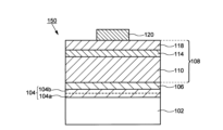
- FIG. 1 is a diagram showing the structure of a light-emitting device including the configuration of a laminated structure according to one embodiment of the present invention
- FIG. 1 is a diagram showing the structure of a light-emitting device including the configuration of a laminated structure according to one embodiment of the present invention
- FIG. 1 is a diagram showing the structure of a transistor including the configuration of a stacked structure according to one embodiment of the present invention
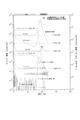
- FIG. 4 is a diagram showing the results of measuring the contents of oxygen, carbon, hydrogen, and fluorine contained in gallium nitride layers shown in Examples by secondary ion mass spectrometry.
- a member or region when a member or region is “above (or below)” another member or region, it means directly above (or directly below) the other member or region unless otherwise specified. Includes not only one case but also the case above (or below) another member or region, that is, the case where another component is included between above (or below) another member or region .
- FIG. 1 shows an example of the structure of a laminated structure 100 according to an embodiment of the present invention.
- the laminated structure 100 includes an amorphous substrate 102 , a buffer layer 106 provided on the amorphous substrate 102 , and a gallium nitride based semiconductor layer 108 provided on the buffer layer 106 .
- the laminated structure 100 may include a base insulating layer 104 between the amorphous substrate 102 and the buffer layer 106 .
- the amorphous substrate 102 preferably has a low thermal expansion coefficient, a high strain point, and a high surface flatness.
- the amorphous substrate 102 preferably has an expansion coefficient of less than 50 ⁇ 10 ⁇ 7 /° C. and a strain point of 600° C. or higher.
- the amorphous substrate 102 in this embodiment only needs to have heat resistance of about 700° C., and is not required to have heat resistance of 1000° C. or more like a sapphire substrate.
- the amorphous substrate 102 preferably contains 0.1% or less of an alkali metal such as sodium (Na).
- a glass substrate made of at least one kind of aluminoborosilicate glass and aluminosilicate glass can be used, and an alkali-free glass substrate is preferable.
- Such glass substrates are used in liquid crystal displays and organic electroluminescence (organic EL) displays, and large-area glass substrates called mother glass are provided on the market.
- organic EL organic electroluminescence
- mother glass large-area glass substrates called mother glass are provided on the market.
- amorphous substrate 102 it is also possible to use a flexible resin substrate such as a polyimide substrate, an acrylic substrate, a siloxane substrate, or a fluorine resin substrate.
- a quartz glass substrate can also be used as the amorphous substrate 102 .
- a base insulating layer 104 may be provided on the amorphous substrate 102 .
- the base insulating layer 104 is formed using an inorganic insulating film.
- As the inorganic insulating film a silicon nitride film, a silicon oxide film, a silicon oxynitride film, an aluminum nitride film, an aluminum oxide film, an aluminum oxynitride film, or the like can be used.
- the base insulating layer 104 has a single-layer structure of these inorganic insulating films or a laminated structure of a plurality of inorganic insulating films.
- FIG. 1 shows the case where the base insulating layer 104 has a laminated structure.
- FIG. 1 shows an example in which the base insulating layer 104 is formed of a silicon nitride layer 104a provided in contact with the amorphous substrate 102 and a silicon oxide layer 104b provided thereon.
- the silicon nitride layer 104a has the effect of preventing impurities contained in the amorphous substrate 102 from diffusing into the buffer layer 106 and the gallium nitride based semiconductor layer 108.
- a particularly problematic impurity is an alkali metal such as sodium contained in the amorphous substrate 102 in a trace amount. If the silicon nitride layer 104a has a film thickness of 20 nm or more, the diffusion of alkali metal can be prevented.
- the film thickness of the silicon nitride layer 104a can be, for example, 20 nm or more and 500 nm or less, preferably 100 nm or more and 300 nm or less, and can be formed with a film thickness of 150 nm, for example.
- the silicon oxide layer 104b can improve adhesion of the buffer layer 106 and prevent peeling.
- the silicon oxide layer 104b preferably has a thickness of 20 nm or more.
- the thickness of the silicon oxide layer 104b can be, for example, 20 nm or more and 500 nm or less, preferably 50 nm or more and 200 nm or less, and can be formed with a thickness of 100 nm, for example.
- the gallium nitride-based semiconductor layer 108 By providing the underlying insulating layer 104 on the amorphous substrate 102, diffusion of impurities into the gallium nitride based semiconductor layer 108 can be prevented, and high purity can be achieved. Thereby, the gallium nitride-based semiconductor layer 108 with high crystallinity can be formed.
- Buffer Layer A buffer layer 106 is provided over the amorphous substrate 102 .
- the buffer layer 106 preferably has crystallinity, that is, at least one of a crystalline metal and a metal compound. Crystals of the buffer layer 106 have an orientation, and the orientation is preferably c-axis orientation.
- the buffer layer 106 is preferably a crystal having rotational symmetry, for example, the crystal surface preferably has six-fold symmetry.
- the buffer layer 106 preferably has a hexagonal close-packed structure, a face-centered cubic structure, or a structure conforming to these.
- the structure conforming to the hexagonal close-packed structure or the face-centered cubic structure includes a crystal structure in which the c-axis is not 90 degrees with respect to the a-axis and the b-axis.
- the buffer layer 106 using a conductive material having a hexagonal close-packed structure or a similar structure is oriented in the (0001) direction, that is, in the c-axis direction with respect to the amorphous substrate 102 (hereinafter referred to as hexagonal close-packed structure). (0001) orientation of the dense structure is preferred.
- the buffer layer 106 having a face-centered cubic structure or a structure similar thereto is oriented in the (111) direction with respect to the amorphous substrate 102 (hereinafter referred to as the (111) orientation of the face-centered cubic structure). is preferred.
- the buffer layer 106 is provided between the amorphous substrate 102 and the gallium nitride based semiconductor layer 108 . Since the gallium nitride-based semiconductor layer 108 having crystallinity is formed on the amorphous substrate 102, the buffer layer 106 functions as a buffer layer that alleviates lattice mismatch. Crystallization of the gallium nitride based semiconductor layer 108 can be achieved by the buffer layer 106 having the above crystallinity.
- the buffer layer 106 has a c-axis orientation and has a crystalline surface having six-fold rotational symmetry such as a hexagonal close-packed structure or a face-centered cubic structure, so that the c-axis of the gallium nitride-based semiconductor layer 108 is Orientation can be controlled so as to grow in the film thickness direction.
- the buffer layer 106 preferably has a flat surface.
- the flatness of the surface of the buffer layer 106 is represented by arithmetic mean roughness (Ra), the value is preferably less than 2.5 nm, more preferably less than 2.3 nm.
- the flat surface of the buffer layer 106 can improve the crystallinity of the gallium nitride based semiconductor layer 108 . It is preferable that the Ra of the buffer layer 106 is as small as possible.
- the surface roughness of the buffer layer 106 can be measured with an atomic force microscope (AFM).
- the buffer layer 106 is preferably a thin film while having crystallinity.
- the thickness of the buffer layer 106 is not particularly limited as long as it can be regarded as a thin film. However, if the film thickness is too thin, the flatness of the surface may be poor and the film may not have crystallinity. On the other hand, if the film thickness of the buffer layer 106 is excessively large, crystallization causes a surface morphology peculiar to metal, resulting in deterioration of the flatness of the surface. Therefore, the film thickness of the buffer layer 106 is preferably 5 nm or more and 500 nm or less, more preferably 10 nm or more and 200 nm or less.
- the film thickness of the buffer layer 106 can be measured by a contact-type profilometer or an optical film-thickness meter (ellipsometry), or by a scanning electron microscope (SEM) or a transmission electron microscope (TEM). It can be measured from the image obtained.
- the buffer layer 106 can be made of metal. Titanium (Ti) and aluminum (Al) are preferably used as the metal material for forming the buffer layer 106. In addition, silver (Ag), nickel (Ni), copper (Cu), strontium (Sr), rhodium ( Rh), palladium (Pd), iridium (Ir), platinum (Pt), gold (Au), and the like can be used. In addition, the buffer layer 106 can also use metal oxide materials such as zinc oxide (ZnO) and titanium dioxide (TiO 2 ).
- Such a buffer layer 106 can be produced by a sputtering method or an electron beam vacuum deposition method.
- the buffer layer 106 can be formed of an insulating layer instead of a metal layer. That is, the buffer layer 106 can also be formed using an insulating material.
- the insulating buffer layer 106 aluminum nitride (AlN), aluminum oxide ( Al2O3 ), or the like can be used.
- the insulating buffer layer 106 preferably has the same crystallinity as described above and preferably has the same film thickness.
- the gallium nitride based semiconductor layer 108 includes at least one gallium nitride (GaN) layer.
- the gallium nitride-based semiconductor layer 108 is a single-layer gallium nitride layer.
- the gallium nitride-based semiconductor layer 108 includes a gallium nitride layer, and further includes at least one layer selected from an indium gallium nitride (InGaN) layer and an aluminum gallium nitride (AlGaN) layer, and these layers are laminated. have a structure.
- the gallium nitride layer, the indium gallium nitride layer, and the aluminum gallium nitride layer forming the gallium nitride-based semiconductor layer 108 preferably have a stoichiometric composition. good too.
- the gallium nitride based semiconductor layer 108 preferably has crystallinity. That is, the gallium nitride layer forming the gallium nitride based semiconductor layer 108 preferably has crystallinity.
- the gallium nitride layer is preferably monocrystalline, but may be polycrystalline, microcrystalline, or nanocrystalline.
- the crystal structure of the gallium nitride layer preferably has a wurtzite structure.
- the gallium nitride layer forming the gallium nitride based semiconductor layer 108 preferably has c-axis orientation or (111) orientation.
- the conductivity type of the gallium nitride layer forming part or all of the gallium nitride based semiconductor layer 108 may be substantially intrinsic, or may be n-type or p-type conductivity. good too.
- the gallium nitride layer may contain dopants for valence electron control.
- the n-type gallium nitride layer may be doped with one element selected from silicon (Si) and germanium (Ge) as a dopant.
- the p-type gallium nitride layer may be doped with an element selected from magnesium (Mg), zinc (Zn), cadmium (Cd), and beryllium (Be) as a dopant.
- the n-type gallium nitride layer preferably has a carrier concentration of 1 ⁇ 10 18 /cm 3 or more.
- the p-type gallium nitride layer preferably has a carrier concentration of 5 ⁇ 10 16 /cm 3 or more.
- the substantially intrinsic (in other words, highly resistive) gallium nitride layer may contain zinc (Zn) as a dopant.
- a gallium nitride layer forming part or all of the gallium nitride-based semiconductor layer 108 is provided in contact with the buffer layer 106 .
- a gallium nitride layer is deposited over the buffer layer 106 .
- a gallium nitride layer having a c-axis orientation or (111) orientation is formed.
- the gallium nitride layer may have an amorphous structure near the interface with the buffer layer 106, but preferably has crystallinity in a region (bulk) away from the interface.
- the gallium nitride layer forming part or all of the gallium nitride based semiconductor layer 108 has crystallinity, the performance of the gallium nitride based semiconductor device can be improved.
- the gallium nitride-based semiconductor device is a light-emitting device, it can increase the emission intensity, and if it is an active device such as a transistor, it can increase the carrier mobility.
- the gallium nitride layer forming part or all of the gallium nitride based semiconductor layer 108 contains oxygen (O), carbon (C), hydrogen (H), Fluorine (F) may be included.
- the concentration of oxygen contained in the gallium nitride layer is preferably 2 ⁇ 10 21 /cm 3 or less, more preferably 1 ⁇ 10 21 /cm 3 or less.
- the concentration of carbon contained in the gallium nitride layer is preferably 5 ⁇ 10 19 /cm 3 or less, more preferably 3 ⁇ 10 19 /cm 3 or less.
- the concentration of hydrogen contained in the gallium nitride layer is preferably 3 ⁇ 10 20 /cm 3 or less, more preferably 2 ⁇ 10 20 /cm 3 or less.
- the concentration of fluorine contained in the gallium nitride layer is preferably 1 ⁇ 10 19 /cm 3 or less, more preferably 5 ⁇ 10 17 /cm 3 or less.
- the lower limit values of oxygen (O), carbon (C), hydrogen (H), and fluorine (F) as impurity elements are not limited from the viewpoint of achieving high purity of the gallium nitride layer, and are preferably as low as possible. However, the lower limit may be equal to or higher than the detection limit of the measuring device for detecting these impurity elements.
- the background level shall be equal to or higher than the background level. can do.
- the lower limits are 6 ⁇ 10 16 /cm 3 or more for oxygen (O), 4 ⁇ 10 16 /cm 3 or more for carbon (C), 2 ⁇ 10 17 /cm 3 or more for hydrogen (H), and 2 ⁇ 10 17 /cm 3 or more for fluorine ( F) can be 2 ⁇ 10 15 /cm 3 or more.
- a high impurity concentration in the gallium nitride layer is not preferable because the crystallinity is lowered and the defect level that becomes a carrier trap increases.
- Oxygen contained in the gallium nitride layer acts as a dopant, so if the above range is exceeded, the conductivity may change, possibly degrading device characteristics.
- Hydrogen contained in the gallium nitride layer may passivate and inactivate the p-type dopant in particular, so it is preferable not to exceed the above range. Since carbon contained in the gallium nitride layer forms crystal defects and forms defect levels to lower the light emission efficiency, it is preferable not to exceed the above range.
- the concentrations of these impurity elements are based on measured values obtained by secondary ion mass spectrometry.
- the above impurity concentration is quantified based on the secondary ion intensity measured in the depth direction (thickness direction of the film) for each element using cesium ions (Cs + ) as primary ions. It is based on the value obtained by performing
- Impurities such as oxygen, hydrogen, carbon, and fluorine contained in the gallium nitride-based semiconductor layer 108 originate from impurities contained in the sputtering target material. Moreover, these impurity elements originate from the residual gas in the film forming chamber of the sputtering apparatus. Impurity elements contained in the gallium nitride layer are considered to be incorporated into the film from these sources during sputtering film formation. These impurity elements are different from impurities intentionally added for the purpose of controlling valence electrons, and can be said to be unavoidable impurities.
- the concentrations of oxygen, carbon, hydrogen, and fluorine that are inevitably contained in the gallium nitride layer forming part or all of the gallium nitride-based semiconductor layer 108 are highly purified so that they fall within the numerical ranges described above. , the crystallinity of the gallium nitride layer can be enhanced. Namely.
- the crystallinity of the gallium nitride-based semiconductor layer 108 provided on the amorphous substrate 102 is improved by improving the purity of the gallium nitride layer forming part or all of the gallium nitride-based semiconductor layer 108 . can increase
- Method for Producing Laminated Structure There is no particular limitation on the method for producing the laminated structure 100 according to the present embodiment. However, the laminated structure 100 according to this embodiment can be favorably produced according to the following production method.
- the laminated structure 100 is manufactured by a manufacturing method including a step of forming a buffer layer 106 on an amorphous substrate 102 and a step of forming a gallium nitride based semiconductor layer 108 on the buffer layer 106. can be made.
- a step of forming the base insulating layer 104 on the amorphous substrate 102 is included before forming the buffer layer 106 .
- the step of forming the gallium nitride-based semiconductor layer 108 includes a film formation step using a sputtering method. The following description includes the step of forming the base insulating layer 104 .
- a glass substrate is used as the amorphous substrate 102 .
- the glass substrate is a non-alkali glass substrate made of aluminoborosilicate glass, aluminosilicate glass, or the like.
- Amorphous substrate 102 is cleaned to form a clean surface.
- any cleaning method may be used, for example, cleaning is performed with a mixed cleaning solution containing sulfuric acid and hydrogen peroxide or hydrochloric acid and hydrogen peroxide, followed by ultrapure water rinsing to wash away the mixed cleaning solution.
- the base insulating layer 104 is formed of a silicon nitride layer 104a and a silicon oxide layer 104b. There is no limitation on the method for forming the silicon nitride layer 104a and the silicon oxide layer 104b.
- the silicon nitride layer 104a is formed by a plasma CVD (Chemical Vapor Deposition) method using reactive gases such as silane (SiH 4 ), ammonia (NH 3 ), and nitrogen (N 2 ), and the silicon oxide layer 104b is formed by It is produced by a plasma CVD method using raw material gases such as silane (SiH 4 ), nitrous oxide (N 2 O), tetraethyl orthosilicate (TEOS).
- the silicon nitride layer 104a and the silicon oxide layer 104b can be deposited continuously.
- the silicon nitride layer 104a may be formed by reactive sputtering using silicon as a sputtering target, and the silicon oxide layer 104b may be formed using quartz as a sputtering target.
- the silicon nitride layer 104a is formed with a thickness of 20 nm or more and 500 nm or less, preferably 100 nm or more and 300 nm or less, for example, 150 nm.
- the silicon oxide layer 104b is formed with a thickness of 20 nm to 500 nm, preferably 50 nm to 200 nm, for example, 100 nm.
- Buffer Layer A buffer layer 106 is formed over the base insulating layer 104 .
- the buffer layer 106 is produced by a sputtering method or a vacuum deposition method.
- a known sputtering method can be used as the sputtering method.
- Known techniques include DC sputtering, RF sputtering, AC sputtering, DC magnetron sputtering, RF magnetron sputtering, pulse sputtering, and ion beam sputtering, induced plasma assisted sputtering.
- DC magnetron sputtering method or RF magnetron sputtering method is preferably applied in order to uniformly form a film on a large glass substrate at high speed.
- the buffer layer 106 When fabricating the buffer layer 106 by sputtering, a metal target, an oxide target, or a nitride target is used as a sputtering target. Since the buffer layer 106 preferably has an orientation, the target material preferably has a high purity, and preferably has a purity of 5N (99.999%) or higher. Moreover, in order to suppress the generation of particles by preventing the occurrence of abnormal discharge, it is preferable to use a target material with a low defect density and a smooth surface.
- the buffer layer 106 When a metal buffer layer is formed as the buffer layer 106, it is preferable to use titanium (Ti) and aluminum (Al) as the metal material as described above, and silver (Ag), nickel (Ni), and copper. (Cu), strontium (Sr), rhodium (Rh), palladium (Pd), iridium (Ir), platinum (Pt), and gold (Au).
- the buffer layer 106 may be formed of a metal oxide such as zinc oxide (ZnO) or titanium dioxide (TiO 2 ) instead of metal.
- the buffer layer 106 may be formed of an insulating material such as aluminum nitride (AlN) or aluminum oxide (Al 2 O 3 ). The thickness of the buffer layer 106 is 5 nm to 500 nm, preferably 10 nm to 200 nm.
- the buffer layer 106 When the buffer layer 106 is made of metal, a high-purity metal is used as a sputtering target.
- a high-purity metal is used as a sputtering target.
- a metal oxide When the buffer layer 106 is formed of a metal oxide, a sintered body of metal oxide is used as a sputtering target.
- a sintered body of an insulating material is used as a sputtering target.
- These target materials are used by being brazed to a backing plate made of copper (Cu), aluminum (Al), stainless steel, or the like.
- the backing plate may be integrally formed.
- the buffer layer 106 is formed by a sputtering method
- the ultimate vacuum of the film formation chamber of the sputtering apparatus is 1 ⁇ 10 ⁇ 4 Pa or less.
- the substrate it is preferable to heat the substrate to 100.degree. C. to 300.degree.
- the gallium nitride based semiconductor layer 108 is produced by a sputtering method.
- a gallium nitride-based sintered body is used as a sputtering target.
- a gallium nitride layer is formed as the gallium nitride-based semiconductor layer 108
- a gallium nitride sintered body is used as the target material of the sputtering target. From the viewpoint of enhancing the crystallinity of the gallium nitride layer, it is preferable that the amount of oxygen contained in the sputtering target material is as low as possible.
- the oxygen content of the gallium nitride sintered body used as the target material is preferably 3 atomic % or less, more preferably 1 atomic % or less.
- the content of metal impurities other than gallium is preferably less than 0.1 at %, more preferably less than 0.01 at %.
- the target material made of the gallium nitride sintered body preferably has a resistivity of 1 ⁇ 10 2 ⁇ cm or less and a density of 3.0 g/cm 3 or more and 5.4 g/cm 3 or less. No precipitation is preferred.
- the area of the sputtering target is preferably 18 cm 2 or more, more preferably 100 cm 2 or more.
- a DC sputtering method As a sputtering method, a DC sputtering method, an RF sputtering method, an AC sputtering method, a DC magnetron sputtering method, an RF magnetron sputtering method, a pulse sputtering method, an ion beam sputtering method, and an induced plasma-assisted sputtering method can be used.
- the DC magnetron sputtering method and the RF magnetron sputtering method are preferable because they can cope with an increase in the area of the amorphous substrate 102 .
- it is preferable to employ a moving magnet method which enables the entire surface of the sputtering target to be eroded, thereby enabling effective use of materials.
- the gas pressure during film formation of the gallium nitride layer by sputtering is less than 0.3 Pa, preferably 0.1 Pa or less, and more preferably 0.08 Pa or less.
- the lower the gas pressure during sputtering film formation the more the sputtered particles adhering to the deposition surface can be diffused, and the crystallinity can be improved.
- the ultimate vacuum of the film formation chamber of the sputtering apparatus is preferably 3 ⁇ 10 ⁇ 5 Pa or less, more preferably 1 ⁇ 10 ⁇ 5 Pa or less.
- the amorphous substrate 102 (that is, the surface of the buffer layer 106 that becomes the deposition surface) is preferably reverse-sputtered.
- Reverse sputtering is a method of cleaning the surface by irradiating the amorphous substrate 102 side with rare gas ions such as argon (Ar) instead of the sputtering target side.
- Ar argon
- the sputtering apparatus is preferably provided with a dedicated processing chamber for performing reverse sputtering in addition to the film forming chamber. It is possible to form a film while maintaining the cleanliness of the surface of the substrate 102 (that is, the surface of the buffer layer 106 serving as the deposition surface).
- the substrate temperature (also referred to as “film formation temperature”) during sputtering film formation is preferably room temperature to 600° C. or lower, more preferably 100° C. or higher and 400° C. or lower. In addition, if the temperature is higher than 600° C., the heat resistance temperature of the amorphous substrate 102 is exceeded, and the cost of the sputtering apparatus becomes high, reducing the advantage of using the sputtering method.
- the substrate temperature may be room temperature (including the case where the substrate is not intentionally heated) or higher. The crystallinity of the gallium nitride layer deposited on layer 106 can be improved.
- a rare gas such as argon (Ar) is usually used as a gas for sputtering (sputtering gas), but nitrogen (N 2 ) gas is preferably used in forming a gallium nitride film.
- nitrogen gas is usually used as the sputtering gas, generation of nitrogen defects can be suppressed.
- the power density during discharge is preferably 5 W/cm 2 or less, more preferably 2.5 W/cm 2 or less, and even more preferably 1.5 W/cm 2 or less.
- the lower limit is preferably 0.1 W/cm 2 or more, more preferably 0.3 W/cm 2 or more.
- the power density is calculated by dividing the power applied during discharge by the area of the sputtering target material. If the electric power during discharge is higher than 5 W/cm 2 , coarse polycrystalline particles tend to peel off from the sputtering target. If the power density is less than 0.1 W/cm 2 , the discharge becomes stable and the film formation speed decreases, resulting in a decrease in film productivity.
- the film thickness of the gallium nitride layer is preferably 30 nm or more, more preferably 50 nm or more. With such a film thickness, a gallium nitride layer having crystallinity can be formed on the buffer layer 106 . Further, the film thickness of the gallium nitride layer may be 5000 nm or less, preferably 1000 nm or less, more preferably 200 nm to 500 nm or less.
- the gallium nitride-based semiconductor layer 108 is a gallium nitride layer, but by changing the material of the sputtering target, an indium gallium nitride (InGaN) layer and an aluminum gallium nitride (AlGaN) layer can be obtained. Crystalline thin films with different compositions, such as layers, can be fabricated.
- a gallium nitride-based semiconductor layer 108 in which a plurality of layers with different compositions are stacked can be formed by mounting sputtering targets with different compositions in each film formation chamber. can.
- the concentration of impurities such as oxygen contained in the sputtering target material is reduced, high vacuum evacuation is performed during the sputtering film formation, and a process such as reverse sputtering is performed.
- the gallium nitride-based semiconductor layer 108 with low concentration of impurities such as oxygen, carbon, hydrogen, and fluorine and high crystallinity can be produced.
- the oxygen concentration is 2 ⁇ 10 21 /cm 3 or less, preferably 1 ⁇ 10 21 /cm 3 or less
- the carbon concentration is 5 ⁇ 10 19 /cm 3 or less, preferably 3 ⁇ 10 19 /cm 3 or less
- the hydrogen concentration is 3 ⁇ 10 20 /cm 3 or less, preferably 2 ⁇ 10 20 /cm 3 or less
- the fluorine concentration is 1 ⁇ 10 19 /cm 3 or less, preferably 5 ⁇ 10 17 /cm 3 or less. It is possible to fabricate a gallium nitride layer with With such an impurity concentration, the laminated structure 100 in which the crystalline gallium nitride based semiconductor layer 108 is formed on the amorphous substrate 102 can be produced.
- the gallium nitride-based semiconductor layer 108 uses a sputtering target made of gallium nitride with reduced impurities such as oxygen, and the amorphous substrate 102 is subjected to a process such as reverse sputtering. After being evacuated to a high vacuum, it is produced by the sputtering method at the predetermined power density.
- the concentration of impurities such as oxygen, carbon, and hydrogen is reduced, and the gallium nitride based semiconductor layer 108 with high crystallinity and low defect density can be obtained.
- Gallium Nitride-Based Semiconductor Device such as light-emitting devices and transistors can be manufactured from the laminated structure 100 according to the present embodiment.
- An example of a device having the laminated structure 100 as a basic structure is shown below. Note that the device shown below is an example, and the device realized by the laminated structure 100 is not limited to the illustrated structure.
- FIG. 2A shows a light emitting device 150 as an example of a gallium nitride based semiconductor device.
- the light-emitting device 150 has a laminated structure 100 in which a base insulating layer 104 , a buffer layer 106 and a gallium nitride based semiconductor layer 108 are laminated on an amorphous substrate 102 .
- the gallium nitride based semiconductor layer 108 has a structure in which an n-type gallium nitride layer 110, a light emitting layer 114, and a p-type gallium nitride layer 118 are laminated.
- An upper electrode layer 120 is provided on the p-type gallium nitride layer 118 .
- the upper electrode layer 120 is formed of a metal material such as gold (Au), a titanium (Ti)-gold (Au) alloy, or a transparent conductive film such as indium tin oxide (ITO).
- the structure of the light emitting layer 114 may vary, and may be formed by quantum well layers in which gallium nitride (GaN) layers and indium gallium nitride (InGaN) layers are alternately stacked.
- FIG. 2B shows a light-emitting device 155 in which the configuration of the gallium nitride-based semiconductor layer 108 is different from that in FIG. 2A.
- the light-emitting device 155 has a structure in which an n-type gallium nitride layer 110, an n-type aluminum gallium nitride layer 112, an indium gallium nitride layer 114 as a light-emitting layer, a p-type aluminum gallium nitride layer 116, and a p-type gallium nitride layer 118 are laminated. have. Since each of these layers has a different composition, they are formed using a sputtering target corresponding to each composition.
- the light-emitting device 150 shown in FIG. 2A and the light-emitting device 155 shown in FIG. 2B include the structure of the laminated structure 100 shown in this embodiment.
- the laminated structure 100 has a gallium nitride-based semiconductor layer 108 having a reduced concentration of impurities such as oxygen, carbon, and hydrogen and having high crystallinity on an amorphous substrate 102 . Since the gallium nitride-based semiconductor layer 108 can be formed on a large-area amorphous substrate 102, the number of light-emitting devices that can be separated from one amorphous substrate 102 can be increased. Productivity can be improved. Also, an LED array can be produced by arranging light emitting devices on the amorphous substrate 102, and a display device can be produced from the LED array.
- Transistor FIG. 3 shows a transistor 160 as an example of a gallium nitride based semiconductor device.
- Transistor 160 includes gallium nitride based semiconductor layer 108 formed on amorphous substrate 102 .
- the gallium nitride-based semiconductor layer 108 has a structure in which an n + -type gallium nitride layer 122, an n-type gallium nitride layer 124, a p-type gallium nitride layer 126, and an n-type gallium nitride layer 128 are laminated.
- the gate electrode 132 is provided so as to be embedded in the p-type gallium nitride layer 126 with the gate insulating layer 130 interposed therebetween.
- a source electrode 134 is provided on the n-type gallium nitride layer 128 .
- the buffer layer 106 may also function as the drain electrode. That is, by forming the buffer layer 106 using a metal or a conductive metal oxide, it can also function as a drain electrode.
- the transistor 160 shown in FIG. 3 can be used, for example, as a power transistor.
- the active layer of the transistor 160 is formed by the gallium nitride-based semiconductor layer 108 provided on the amorphous substrate 102 .
- the gallium nitride-based semiconductor layer 108 has high crystallinity with a reduced concentration of impurities such as oxygen, carbon, and hydrogen, and a reduced defect density. can be provided in
- a non-alkali glass substrate was used as the amorphous substrate 102 .
- a silicon nitride layer 104a with a thickness of 150 nm and a silicon oxide layer 104b with a thickness of 100 nm were formed on a non-alkali glass substrate.
- the silicon nitride layer 104a and the silicon oxide layer 104b were formed by plasma CVD.
- the silicon nitride layer 104a was formed using silane (SiH 4 ), ammonia (NH 3 ), and nitrogen (N 2 ) as reaction gases at an RF power density of 0.24 W/cm 2 and a substrate temperature of 400°C.
- the silicon oxide layer 104b was formed using silane (SiH 4 ) and nitrous oxide (N 2 O) as reaction gases at an RF power density of 0.61 W/cm 2 and a substrate temperature of 380°C.
- a titanium (Ti) layer having a thickness of 50 nm was formed as a buffer layer 106 on the underlying insulating layer 104 .
- the titanium (Ti) layer was formed by a sputtering method using a titanium (Ti) target at room temperature without heating the substrate.
- a gallium nitride layer was formed as the gallium nitride-based semiconductor layer 108 by a sputtering method.
- Sputtering conditions are as follows.
- Discharge method RF sputtering Film forming device: Magnetron sputtering device
- Target material Gallium nitride (oxygen content 7 atm%)
- Target size 120mm ⁇
- Target-substrate distance 150mm
- Deposition pressure 0.3 Pa
- Introduced gas Nitrogen Discharge power: 100W Film formation temperature: 200°C Film thickness: 100 nm Heat treatment temperature: 600°C
- the impurity concentration of the gallium nitride layer produced under the above conditions was evaluated by secondary ion mass spectrometry. As impurities contained in the gallium nitride layer, concentrations of oxygen, hydrogen, carbon, and fluorine were measured.
- Measuring device PHI ADEPT1010
- Primary ion species Cs + Primary acceleration voltage: 2.0 kV
- Detection area 90 ⁇ m ⁇ 90 ⁇ m
- FIG. 4 shows a graph showing the distribution in the depth direction of each element of oxygen, hydrogen, carbon, and fluorine contained in the gallium nitride layer measured by secondary ion mass spectrometry.
- the horizontal axis indicates the depth from the surface of the gallium nitride film, and the vertical axis indicates the concentration converted from the secondary ion intensity of each element.
- the graph shown in FIG. 4 shows the Back-Geland level (detection limit) of each element of oxygen, hydrogen, carbon, and fluorine.
- the background is 6.0 ⁇ 10 16 /cm 3 oxygen, 2.1 ⁇ 10 17 /cm 3 hydrogen, 4.5 ⁇ 10 16 /cm 3 carbon, and 1.9 ⁇ 10 15 /cm fluorine. 3 .
- the graph shown in FIG. 4 also shows the secondary ion intensities of gallium (Ga)+nitrogen (N), gallium (Ga), and titanium (Ti) as matrix markers.
- the part where the secondary ion intensity of gallium (Ga) + nitrogen (N) and gallium (Ga) is flat, which is shown as a matrix marker, is the gallium nitride layer. range. From the graph of FIG. 4, it can be seen that the gallium nitride layer extends from the surface to about 80 ⁇ m, and the titanium layer as the buffer layer exists after that. Quantitative values of oxygen, hydrogen, carbon, and fluorine can be read from the area where the matrix marker is flat. Due to the characteristics of secondary ion mass spectrometry, profile pile-up is observed near the film surface and near the interface due to charge-up and impurity contamination, so these portions should not be taken into consideration.
- Table 1 shows the respective concentrations of oxygen, hydrogen, carbon, and fluorine contained in the gallium nitride layer read from the graph shown in FIG.
- the gallium nitride layer produced in this example had a hydrogen concentration of 9.7 ⁇ 10 19 /cm 3 , a carbon concentration of 1.4 ⁇ 10 19 /cm 3 , and an oxygen concentration of 7.7 ⁇ 10 19 /cm 3 .
- 1 ⁇ 10 20 /cm 3 and a fluorine concentration of 1.9 ⁇ 10 17 /cm 3 were obtained.
- the profile of hydrogen shows a tendency to gradually decrease from the surface to the inside of the gallium nitride layer, but when reading quantitative values, the values near the center of the film are read.
- impurities that are inevitably introduced when a gallium nitride film is formed by a sputtering method are reduced as much as possible even when an amorphous substrate such as a glass substrate is used. shows that a gallium nitride layer with excellent crystallinity can be produced even when an amorphous substrate is used.
- 100 laminated structure, 102: amorphous substrate, 104: underlying insulating layer, 106: buffer layer, 108: gallium nitride based semiconductor layer, 110: n-type gallium nitride layer, 112: n-type aluminum gallium nitride layer, 114 : light emitting layer, 115: indium gallium nitride layer, 116: p-type aluminum gallium nitride layer, 118: p-type gallium nitride layer, 120: upper electrode layer, 122: n + type gallium nitride layer, 124: n-type gallium nitride layer, 126: p-type gallium nitride layer, 128: n-type gallium nitride layer, 130: gate insulating layer, 132: gate electrode, 134: source electrode, 150: light emitting device, 155: light emitting device, 160: transistor
Landscapes
- Chemical & Material Sciences (AREA)
- Chemical Kinetics & Catalysis (AREA)
- Engineering & Computer Science (AREA)
- Materials Engineering (AREA)
- Mechanical Engineering (AREA)
- Metallurgy (AREA)
- Organic Chemistry (AREA)
- Recrystallisation Techniques (AREA)
Priority Applications (2)
| Application Number | Priority Date | Filing Date | Title |
|---|---|---|---|
| JP2023556301A JP7757413B2 (ja) | 2021-10-28 | 2022-10-12 | 積層構造体及び窒化ガリウム系半導体デバイス |
| US18/647,501 US20240282889A1 (en) | 2021-10-28 | 2024-04-26 | Stacked structure and gallium nitride-based semiconductor device |
Applications Claiming Priority (2)
| Application Number | Priority Date | Filing Date | Title |
|---|---|---|---|
| JP2021176842 | 2021-10-28 | ||
| JP2021-176842 | 2021-10-28 |
Related Child Applications (1)
| Application Number | Title | Priority Date | Filing Date |
|---|---|---|---|
| US18/647,501 Continuation US20240282889A1 (en) | 2021-10-28 | 2024-04-26 | Stacked structure and gallium nitride-based semiconductor device |
Publications (1)
| Publication Number | Publication Date |
|---|---|
| WO2023074374A1 true WO2023074374A1 (ja) | 2023-05-04 |
Family
ID=86157987
Family Applications (1)
| Application Number | Title | Priority Date | Filing Date |
|---|---|---|---|
| PCT/JP2022/038069 Ceased WO2023074374A1 (ja) | 2021-10-28 | 2022-10-12 | 積層構造体及び窒化ガリウム系半導体デバイス |
Country Status (4)
| Country | Link |
|---|---|
| US (1) | US20240282889A1 (https=) |
| JP (1) | JP7757413B2 (https=) |
| TW (1) | TWI834343B (https=) |
| WO (1) | WO2023074374A1 (https=) |
Cited By (2)
| Publication number | Priority date | Publication date | Assignee | Title |
|---|---|---|---|---|
| WO2025075016A1 (ja) * | 2023-10-02 | 2025-04-10 | 東ソー株式会社 | 窒化ガリウム膜、その製造方法、積層基材、半導体素子及び電子機器 |
| WO2025164205A1 (ja) * | 2024-01-29 | 2025-08-07 | 株式会社ジャパンディスプレイ | 積層構造体、および積層構造体の作製方法 |
Families Citing this family (1)
| Publication number | Priority date | Publication date | Assignee | Title |
|---|---|---|---|---|
| US20240363342A1 (en) * | 2023-04-27 | 2024-10-31 | Robert Bosch Gmbh | METHODS AND STRUCTURES FOR REDUCING DEFORMATIONS OF GALLIUM NITRIDE (GaN) DEVICES |
Citations (6)
| Publication number | Priority date | Publication date | Assignee | Title |
|---|---|---|---|---|
| JP2008306114A (ja) * | 2007-06-11 | 2008-12-18 | Showa Denko Kk | Iii族窒化物半導体の製造方法、iii族窒化物半導体発光素子の製造方法、及びiii族窒化物半導体発光素子、並びにランプ |
| JP2012119569A (ja) * | 2010-12-02 | 2012-06-21 | Ulvac Japan Ltd | 窒化物半導体素子 |
| JP2013212978A (ja) * | 2012-03-30 | 2013-10-17 | Mitsubishi Chemicals Corp | Iii族窒化物結晶塊 |
| JP2018046277A (ja) * | 2016-09-13 | 2018-03-22 | 東ソー株式会社 | 窒化ガリウム系膜ならびにその製造方法 |
| WO2020075599A1 (ja) * | 2018-10-09 | 2020-04-16 | 東京エレクトロン株式会社 | 窒化物半導体膜の形成方法 |
| JP2021163900A (ja) * | 2020-04-01 | 2021-10-11 | 株式会社ジャパンディスプレイ | 発光素子および表示装置 |
-
2022
- 2022-10-12 WO PCT/JP2022/038069 patent/WO2023074374A1/ja not_active Ceased
- 2022-10-12 JP JP2023556301A patent/JP7757413B2/ja active Active
- 2022-10-18 TW TW111139415A patent/TWI834343B/zh active
-
2024
- 2024-04-26 US US18/647,501 patent/US20240282889A1/en active Pending
Patent Citations (6)
| Publication number | Priority date | Publication date | Assignee | Title |
|---|---|---|---|---|
| JP2008306114A (ja) * | 2007-06-11 | 2008-12-18 | Showa Denko Kk | Iii族窒化物半導体の製造方法、iii族窒化物半導体発光素子の製造方法、及びiii族窒化物半導体発光素子、並びにランプ |
| JP2012119569A (ja) * | 2010-12-02 | 2012-06-21 | Ulvac Japan Ltd | 窒化物半導体素子 |
| JP2013212978A (ja) * | 2012-03-30 | 2013-10-17 | Mitsubishi Chemicals Corp | Iii族窒化物結晶塊 |
| JP2018046277A (ja) * | 2016-09-13 | 2018-03-22 | 東ソー株式会社 | 窒化ガリウム系膜ならびにその製造方法 |
| WO2020075599A1 (ja) * | 2018-10-09 | 2020-04-16 | 東京エレクトロン株式会社 | 窒化物半導体膜の形成方法 |
| JP2021163900A (ja) * | 2020-04-01 | 2021-10-11 | 株式会社ジャパンディスプレイ | 発光素子および表示装置 |
Cited By (2)
| Publication number | Priority date | Publication date | Assignee | Title |
|---|---|---|---|---|
| WO2025075016A1 (ja) * | 2023-10-02 | 2025-04-10 | 東ソー株式会社 | 窒化ガリウム膜、その製造方法、積層基材、半導体素子及び電子機器 |
| WO2025164205A1 (ja) * | 2024-01-29 | 2025-08-07 | 株式会社ジャパンディスプレイ | 積層構造体、および積層構造体の作製方法 |
Also Published As
| Publication number | Publication date |
|---|---|
| US20240282889A1 (en) | 2024-08-22 |
| JP7757413B2 (ja) | 2025-10-21 |
| TW202328021A (zh) | 2023-07-16 |
| TWI834343B (zh) | 2024-03-01 |
| JPWO2023074374A1 (https=) | 2023-05-04 |
Similar Documents
| Publication | Publication Date | Title |
|---|---|---|
| JP7757413B2 (ja) | 積層構造体及び窒化ガリウム系半導体デバイス | |
| US8278656B2 (en) | Substrate for the epitaxial growth of gallium nitride | |
| JP5661509B2 (ja) | 積層体およびその製造方法、並びにそれを用いた機能素子 | |
| US8785927B2 (en) | Laminate structure including oxide semiconductor thin film layer, and thin film transistor | |
| US9331207B2 (en) | Oxide semiconductor device and manufacturing method therof | |
| CN105658848B (zh) | n型氮化铝单晶基板以及垂直型氮化物半导体器件 | |
| US20250079257A1 (en) | Gallium nitride-based semiconductor device and method for manufacturing the same | |
| JP6143423B2 (ja) | 半導体装置の製造方法 | |
| JP2009141221A (ja) | ZnO半導体膜の製造方法、ZnO半導体膜及びこれを用いた半導体装置 | |
| JP2013183001A (ja) | 半導体装置 | |
| JP6199608B2 (ja) | 光電変換装置 | |
| US20250287623A1 (en) | Rectifying device | |
| US20250133874A1 (en) | Gallium nitride-based semiconductor device on amorphous substrate and method for manufacturing the same | |
| CN108546993A (zh) | 一种沿[101]晶向生长的金红石结构钽掺杂氧化锡单晶薄膜及其制备方法 | |
| JP7827253B2 (ja) | 圧電体膜の製造方法、圧電素子の製造方法及び圧電デバイスの製造方法 | |
| TW201309826A (zh) | 氧化亞錫薄膜的製作方法 | |
| CN111733456B (zh) | 用于AlN单晶生长的复合籽晶及其制备方法 | |
| JP6934473B2 (ja) | Iii族窒化物半導体発光素子 | |
| TW202223144A (zh) | 半導體層疊體、半導體元件及半導體元件的製造方法 | |
| US9219254B2 (en) | Method of forming nanocrystals and method of manufacturing an organic light-emitting display apparatus including a thin film having nanocrystals | |
| KR100733915B1 (ko) | 고분자 재료 기판에 완충층이 증착된 투명 전도성 산화막및 그 제조방법 | |
| JP2007258599A (ja) | 半導体素子及び半導体素子の製造方法 |
Legal Events
| Date | Code | Title | Description |
|---|---|---|---|
| 121 | Ep: the epo has been informed by wipo that ep was designated in this application |
Ref document number: 22886703 Country of ref document: EP Kind code of ref document: A1 |
|
| ENP | Entry into the national phase |
Ref document number: 2023556301 Country of ref document: JP Kind code of ref document: A |
|
| NENP | Non-entry into the national phase |
Ref country code: DE |
|
| 122 | Ep: pct application non-entry in european phase |
Ref document number: 22886703 Country of ref document: EP Kind code of ref document: A1 |