WO2023074374A1 - Multilayer structure and gallium-nitride-based semiconductor device - Google Patents
Multilayer structure and gallium-nitride-based semiconductor device Download PDFInfo
- Publication number
- WO2023074374A1 WO2023074374A1 PCT/JP2022/038069 JP2022038069W WO2023074374A1 WO 2023074374 A1 WO2023074374 A1 WO 2023074374A1 JP 2022038069 W JP2022038069 W JP 2022038069W WO 2023074374 A1 WO2023074374 A1 WO 2023074374A1
- Authority
- WO
- WIPO (PCT)
- Prior art keywords
- gallium nitride
- layer
- laminated structure
- buffer layer
- based semiconductor
- Prior art date
Links
- 229910002601 GaN Inorganic materials 0.000 title claims abstract description 186
- JMASRVWKEDWRBT-UHFFFAOYSA-N Gallium nitride Chemical compound [Ga]#N JMASRVWKEDWRBT-UHFFFAOYSA-N 0.000 title claims abstract description 181
- 239000004065 semiconductor Substances 0.000 title claims abstract description 67
- 239000000758 substrate Substances 0.000 claims abstract description 107
- QVGXLLKOCUKJST-UHFFFAOYSA-N atomic oxygen Chemical compound [O] QVGXLLKOCUKJST-UHFFFAOYSA-N 0.000 claims abstract description 29
- 239000001301 oxygen Substances 0.000 claims abstract description 29
- 229910052760 oxygen Inorganic materials 0.000 claims abstract description 29
- 239000001257 hydrogen Substances 0.000 claims abstract description 24
- 229910052739 hydrogen Inorganic materials 0.000 claims abstract description 24
- OKTJSMMVPCPJKN-UHFFFAOYSA-N Carbon Chemical compound [C] OKTJSMMVPCPJKN-UHFFFAOYSA-N 0.000 claims abstract description 23
- 229910052799 carbon Inorganic materials 0.000 claims abstract description 23
- YCKRFDGAMUMZLT-UHFFFAOYSA-N Fluorine atom Chemical compound [F] YCKRFDGAMUMZLT-UHFFFAOYSA-N 0.000 claims abstract description 20
- 239000011737 fluorine Substances 0.000 claims abstract description 20
- 229910052731 fluorine Inorganic materials 0.000 claims abstract description 20
- UFHFLCQGNIYNRP-UHFFFAOYSA-N Hydrogen Chemical compound [H][H] UFHFLCQGNIYNRP-UHFFFAOYSA-N 0.000 claims abstract description 13
- 238000004544 sputter deposition Methods 0.000 claims description 45
- 238000005477 sputtering target Methods 0.000 claims description 24
- VYPSYNLAJGMNEJ-UHFFFAOYSA-N Silicium dioxide Chemical class O=[Si]=O VYPSYNLAJGMNEJ-UHFFFAOYSA-N 0.000 claims description 17
- 239000011521 glass Substances 0.000 claims description 17
- 239000010936 titanium Substances 0.000 claims description 17
- 229910052581 Si3N4 Inorganic materials 0.000 claims description 15
- HQVNEWCFYHHQES-UHFFFAOYSA-N silicon nitride Chemical compound N12[Si]34N5[Si]62N3[Si]51N64 HQVNEWCFYHHQES-UHFFFAOYSA-N 0.000 claims description 15
- 229910052814 silicon oxide Inorganic materials 0.000 claims description 15
- 229910052751 metal Inorganic materials 0.000 claims description 14
- 239000002184 metal Substances 0.000 claims description 14
- 239000010931 gold Substances 0.000 claims description 10
- PXHVJJICTQNCMI-UHFFFAOYSA-N Nickel Chemical compound [Ni] PXHVJJICTQNCMI-UHFFFAOYSA-N 0.000 claims description 9
- KDLHZDBZIXYQEI-UHFFFAOYSA-N Palladium Chemical compound [Pd] KDLHZDBZIXYQEI-UHFFFAOYSA-N 0.000 claims description 9
- RTAQQCXQSZGOHL-UHFFFAOYSA-N Titanium Chemical compound [Ti] RTAQQCXQSZGOHL-UHFFFAOYSA-N 0.000 claims description 9
- 229910044991 metal oxide Inorganic materials 0.000 claims description 9
- 150000004706 metal oxides Chemical class 0.000 claims description 9
- BASFCYQUMIYNBI-UHFFFAOYSA-N platinum Chemical compound [Pt] BASFCYQUMIYNBI-UHFFFAOYSA-N 0.000 claims description 9
- 229910052719 titanium Inorganic materials 0.000 claims description 9
- 239000010949 copper Substances 0.000 claims description 8
- 239000010948 rhodium Substances 0.000 claims description 6
- 229910052782 aluminium Inorganic materials 0.000 claims description 5
- XAGFODPZIPBFFR-UHFFFAOYSA-N aluminium Chemical compound [Al] XAGFODPZIPBFFR-UHFFFAOYSA-N 0.000 claims description 5
- 229910052737 gold Inorganic materials 0.000 claims description 5
- RYGMFSIKBFXOCR-UHFFFAOYSA-N Copper Chemical compound [Cu] RYGMFSIKBFXOCR-UHFFFAOYSA-N 0.000 claims description 4
- 229910052802 copper Inorganic materials 0.000 claims description 4
- PCHJSUWPFVWCPO-UHFFFAOYSA-N gold Chemical compound [Au] PCHJSUWPFVWCPO-UHFFFAOYSA-N 0.000 claims description 4
- BQCADISMDOOEFD-UHFFFAOYSA-N Silver Chemical compound [Ag] BQCADISMDOOEFD-UHFFFAOYSA-N 0.000 claims description 3
- GWEVSGVZZGPLCZ-UHFFFAOYSA-N Titan oxide Chemical compound O=[Ti]=O GWEVSGVZZGPLCZ-UHFFFAOYSA-N 0.000 claims description 3
- XLOMVQKBTHCTTD-UHFFFAOYSA-N Zinc monoxide Chemical compound [Zn]=O XLOMVQKBTHCTTD-UHFFFAOYSA-N 0.000 claims description 3
- 229910052741 iridium Inorganic materials 0.000 claims description 3
- GKOZUEZYRPOHIO-UHFFFAOYSA-N iridium atom Chemical compound [Ir] GKOZUEZYRPOHIO-UHFFFAOYSA-N 0.000 claims description 3
- 229910052759 nickel Inorganic materials 0.000 claims description 3
- 229910052763 palladium Inorganic materials 0.000 claims description 3
- 229910052697 platinum Inorganic materials 0.000 claims description 3
- 239000011347 resin Substances 0.000 claims description 3
- 229920005989 resin Polymers 0.000 claims description 3
- 229910052703 rhodium Inorganic materials 0.000 claims description 3
- MHOVAHRLVXNVSD-UHFFFAOYSA-N rhodium atom Chemical compound [Rh] MHOVAHRLVXNVSD-UHFFFAOYSA-N 0.000 claims description 3
- 229910052709 silver Inorganic materials 0.000 claims description 3
- 239000004332 silver Substances 0.000 claims description 3
- 229910052712 strontium Inorganic materials 0.000 claims description 3
- CIOAGBVUUVVLOB-UHFFFAOYSA-N strontium atom Chemical compound [Sr] CIOAGBVUUVVLOB-UHFFFAOYSA-N 0.000 claims description 3
- 239000010410 layer Substances 0.000 description 284
- 239000010408 film Substances 0.000 description 64
- 239000012535 impurity Substances 0.000 description 29
- 238000000034 method Methods 0.000 description 26
- 230000015572 biosynthetic process Effects 0.000 description 19
- 239000007789 gas Substances 0.000 description 17
- 239000002585 base Substances 0.000 description 15
- IJGRMHOSHXDMSA-UHFFFAOYSA-N Atomic nitrogen Chemical compound N#N IJGRMHOSHXDMSA-UHFFFAOYSA-N 0.000 description 12
- 239000013077 target material Substances 0.000 description 12
- 238000000151 deposition Methods 0.000 description 11
- 150000002431 hydrogen Chemical class 0.000 description 11
- 230000008021 deposition Effects 0.000 description 10
- 238000001755 magnetron sputter deposition Methods 0.000 description 10
- 239000013078 crystal Substances 0.000 description 8
- RNQKDQAVIXDKAG-UHFFFAOYSA-N aluminum gallium Chemical compound [Al].[Ga] RNQKDQAVIXDKAG-UHFFFAOYSA-N 0.000 description 7
- 230000007547 defect Effects 0.000 description 7
- 150000002500 ions Chemical group 0.000 description 7
- 238000004519 manufacturing process Methods 0.000 description 7
- 238000001004 secondary ion mass spectrometry Methods 0.000 description 7
- GYHNNYVSQQEPJS-UHFFFAOYSA-N Gallium Chemical compound [Ga] GYHNNYVSQQEPJS-UHFFFAOYSA-N 0.000 description 6
- 238000004140 cleaning Methods 0.000 description 6
- 239000002019 doping agent Substances 0.000 description 6
- 229910052733 gallium Inorganic materials 0.000 description 6
- 229910052738 indium Inorganic materials 0.000 description 6
- APFVFJFRJDLVQX-UHFFFAOYSA-N indium atom Chemical compound [In] APFVFJFRJDLVQX-UHFFFAOYSA-N 0.000 description 6
- 239000000203 mixture Substances 0.000 description 6
- QGZKDVFQNNGYKY-UHFFFAOYSA-N Ammonia Chemical compound N QGZKDVFQNNGYKY-UHFFFAOYSA-N 0.000 description 4
- XKRFYHLGVUSROY-UHFFFAOYSA-N Argon Chemical compound [Ar] XKRFYHLGVUSROY-UHFFFAOYSA-N 0.000 description 4
- MHAJPDPJQMAIIY-UHFFFAOYSA-N Hydrogen peroxide Chemical compound OO MHAJPDPJQMAIIY-UHFFFAOYSA-N 0.000 description 4
- GQPLMRYTRLFLPF-UHFFFAOYSA-N Nitrous Oxide Chemical compound [O-][N+]#N GQPLMRYTRLFLPF-UHFFFAOYSA-N 0.000 description 4
- BLRPTPMANUNPDV-UHFFFAOYSA-N Silane Chemical compound [SiH4] BLRPTPMANUNPDV-UHFFFAOYSA-N 0.000 description 4
- 238000010586 diagram Methods 0.000 description 4
- 230000001965 increasing effect Effects 0.000 description 4
- 239000000463 material Substances 0.000 description 4
- 229910052757 nitrogen Inorganic materials 0.000 description 4
- 239000002245 particle Substances 0.000 description 4
- 238000005268 plasma chemical vapour deposition Methods 0.000 description 4
- 229910052594 sapphire Inorganic materials 0.000 description 4
- 239000010980 sapphire Substances 0.000 description 4
- 229910000077 silane Inorganic materials 0.000 description 4
- XUIMIQQOPSSXEZ-UHFFFAOYSA-N Silicon Chemical compound [Si] XUIMIQQOPSSXEZ-UHFFFAOYSA-N 0.000 description 3
- 239000003513 alkali Substances 0.000 description 3
- 229910052783 alkali metal Inorganic materials 0.000 description 3
- 150000001340 alkali metals Chemical class 0.000 description 3
- 230000007423 decrease Effects 0.000 description 3
- 238000001514 detection method Methods 0.000 description 3
- 238000009792 diffusion process Methods 0.000 description 3
- 239000011810 insulating material Substances 0.000 description 3
- 239000011159 matrix material Substances 0.000 description 3
- 239000007769 metal material Substances 0.000 description 3
- 229910021421 monocrystalline silicon Inorganic materials 0.000 description 3
- TWNQGVIAIRXVLR-UHFFFAOYSA-N oxo(oxoalumanyloxy)alumane Chemical compound O=[Al]O[Al]=O TWNQGVIAIRXVLR-UHFFFAOYSA-N 0.000 description 3
- 238000001552 radio frequency sputter deposition Methods 0.000 description 3
- 229910052710 silicon Inorganic materials 0.000 description 3
- 239000010703 silicon Substances 0.000 description 3
- 239000011734 sodium Substances 0.000 description 3
- 239000010409 thin film Substances 0.000 description 3
- PIGFYZPCRLYGLF-UHFFFAOYSA-N Aluminum nitride Chemical compound [Al]#N PIGFYZPCRLYGLF-UHFFFAOYSA-N 0.000 description 2
- VEXZGXHMUGYJMC-UHFFFAOYSA-N Hydrochloric acid Chemical compound Cl VEXZGXHMUGYJMC-UHFFFAOYSA-N 0.000 description 2
- DGAQECJNVWCQMB-PUAWFVPOSA-M Ilexoside XXIX Chemical compound C[C@@H]1CC[C@@]2(CC[C@@]3(C(=CC[C@H]4[C@]3(CC[C@@H]5[C@@]4(CC[C@@H](C5(C)C)OS(=O)(=O)[O-])C)C)[C@@H]2[C@]1(C)O)C)C(=O)O[C@H]6[C@@H]([C@H]([C@@H]([C@H](O6)CO)O)O)O.[Na+] DGAQECJNVWCQMB-PUAWFVPOSA-M 0.000 description 2
- QAOWNCQODCNURD-UHFFFAOYSA-N Sulfuric acid Chemical compound OS(O)(=O)=O QAOWNCQODCNURD-UHFFFAOYSA-N 0.000 description 2
- BOTDANWDWHJENH-UHFFFAOYSA-N Tetraethyl orthosilicate Chemical compound CCO[Si](OCC)(OCC)OCC BOTDANWDWHJENH-UHFFFAOYSA-N 0.000 description 2
- 239000005407 aluminoborosilicate glass Substances 0.000 description 2
- 239000005354 aluminosilicate glass Substances 0.000 description 2
- 229910021529 ammonia Inorganic materials 0.000 description 2
- 229910052786 argon Inorganic materials 0.000 description 2
- 238000006243 chemical reaction Methods 0.000 description 2
- 238000005229 chemical vapour deposition Methods 0.000 description 2
- 238000002425 crystallisation Methods 0.000 description 2
- 230000008025 crystallization Effects 0.000 description 2
- 238000010438 heat treatment Methods 0.000 description 2
- 238000001659 ion-beam spectroscopy Methods 0.000 description 2
- 239000004973 liquid crystal related substance Substances 0.000 description 2
- 239000011777 magnesium Substances 0.000 description 2
- 239000003550 marker Substances 0.000 description 2
- 239000001272 nitrous oxide Substances 0.000 description 2
- 239000002356 single layer Substances 0.000 description 2
- 229910052708 sodium Inorganic materials 0.000 description 2
- JBQYATWDVHIOAR-UHFFFAOYSA-N tellanylidenegermanium Chemical compound [Te]=[Ge] JBQYATWDVHIOAR-UHFFFAOYSA-N 0.000 description 2
- 238000001771 vacuum deposition Methods 0.000 description 2
- 229910018072 Al 2 O 3 Inorganic materials 0.000 description 1
- FYYHWMGAXLPEAU-UHFFFAOYSA-N Magnesium Chemical compound [Mg] FYYHWMGAXLPEAU-UHFFFAOYSA-N 0.000 description 1
- 239000004642 Polyimide Substances 0.000 description 1
- 230000002159 abnormal effect Effects 0.000 description 1
- 230000001133 acceleration Effects 0.000 description 1
- NIXOWILDQLNWCW-UHFFFAOYSA-N acrylic acid group Chemical group C(C=C)(=O)O NIXOWILDQLNWCW-UHFFFAOYSA-N 0.000 description 1
- 229910045601 alloy Inorganic materials 0.000 description 1
- 239000000956 alloy Substances 0.000 description 1
- PNEYBMLMFCGWSK-UHFFFAOYSA-N aluminium oxide Inorganic materials [O-2].[O-2].[O-2].[Al+3].[Al+3] PNEYBMLMFCGWSK-UHFFFAOYSA-N 0.000 description 1
- 238000004458 analytical method Methods 0.000 description 1
- 229910052790 beryllium Inorganic materials 0.000 description 1
- ATBAMAFKBVZNFJ-UHFFFAOYSA-N beryllium atom Chemical compound [Be] ATBAMAFKBVZNFJ-UHFFFAOYSA-N 0.000 description 1
- 230000005540 biological transmission Effects 0.000 description 1
- 229910052793 cadmium Inorganic materials 0.000 description 1
- BDOSMKKIYDKNTQ-UHFFFAOYSA-N cadmium atom Chemical compound [Cd] BDOSMKKIYDKNTQ-UHFFFAOYSA-N 0.000 description 1
- 229910052792 caesium Inorganic materials 0.000 description 1
- -1 cesium ions Chemical class 0.000 description 1
- 230000003749 cleanliness Effects 0.000 description 1
- 239000004020 conductor Substances 0.000 description 1
- 238000011109 contamination Methods 0.000 description 1
- PMHQVHHXPFUNSP-UHFFFAOYSA-M copper(1+);methylsulfanylmethane;bromide Chemical compound Br[Cu].CSC PMHQVHHXPFUNSP-UHFFFAOYSA-M 0.000 description 1
- 229910052593 corundum Inorganic materials 0.000 description 1
- 230000000593 degrading effect Effects 0.000 description 1
- 230000006866 deterioration Effects 0.000 description 1
- 229910001873 dinitrogen Inorganic materials 0.000 description 1
- KPUWHANPEXNPJT-UHFFFAOYSA-N disiloxane Chemical class [SiH3]O[SiH3] KPUWHANPEXNPJT-UHFFFAOYSA-N 0.000 description 1
- 238000009826 distribution Methods 0.000 description 1
- 230000000694 effects Effects 0.000 description 1
- 238000005401 electroluminescence Methods 0.000 description 1
- 238000010894 electron beam technology Methods 0.000 description 1
- 238000000572 ellipsometry Methods 0.000 description 1
- 230000002708 enhancing effect Effects 0.000 description 1
- 229910052732 germanium Inorganic materials 0.000 description 1
- GNPVGFCGXDBREM-UHFFFAOYSA-N germanium atom Chemical compound [Ge] GNPVGFCGXDBREM-UHFFFAOYSA-N 0.000 description 1
- AMGQUBHHOARCQH-UHFFFAOYSA-N indium;oxotin Chemical compound [In].[Sn]=O AMGQUBHHOARCQH-UHFFFAOYSA-N 0.000 description 1
- 239000012212 insulator Substances 0.000 description 1
- 230000001678 irradiating effect Effects 0.000 description 1
- 229910052749 magnesium Inorganic materials 0.000 description 1
- 238000005259 measurement Methods 0.000 description 1
- 150000002736 metal compounds Chemical class 0.000 description 1
- 150000004767 nitrides Chemical class 0.000 description 1
- 230000003287 optical effect Effects 0.000 description 1
- 229920001721 polyimide Polymers 0.000 description 1
- 238000001556 precipitation Methods 0.000 description 1
- 238000002360 preparation method Methods 0.000 description 1
- 239000010453 quartz Substances 0.000 description 1
- 239000002994 raw material Substances 0.000 description 1
- 238000005546 reactive sputtering Methods 0.000 description 1
- 239000010935 stainless steel Substances 0.000 description 1
- 229910001220 stainless steel Inorganic materials 0.000 description 1
- 230000003746 surface roughness Effects 0.000 description 1
- 229910021642 ultra pure water Inorganic materials 0.000 description 1
- 239000012498 ultrapure water Substances 0.000 description 1
- 229910001845 yogo sapphire Inorganic materials 0.000 description 1
- 229910052984 zinc sulfide Inorganic materials 0.000 description 1
Images


Classifications
-
- C—CHEMISTRY; METALLURGY
- C23—COATING METALLIC MATERIAL; COATING MATERIAL WITH METALLIC MATERIAL; CHEMICAL SURFACE TREATMENT; DIFFUSION TREATMENT OF METALLIC MATERIAL; COATING BY VACUUM EVAPORATION, BY SPUTTERING, BY ION IMPLANTATION OR BY CHEMICAL VAPOUR DEPOSITION, IN GENERAL; INHIBITING CORROSION OF METALLIC MATERIAL OR INCRUSTATION IN GENERAL
- C23C—COATING METALLIC MATERIAL; COATING MATERIAL WITH METALLIC MATERIAL; SURFACE TREATMENT OF METALLIC MATERIAL BY DIFFUSION INTO THE SURFACE, BY CHEMICAL CONVERSION OR SUBSTITUTION; COATING BY VACUUM EVAPORATION, BY SPUTTERING, BY ION IMPLANTATION OR BY CHEMICAL VAPOUR DEPOSITION, IN GENERAL
- C23C14/00—Coating by vacuum evaporation, by sputtering or by ion implantation of the coating forming material
- C23C14/06—Coating by vacuum evaporation, by sputtering or by ion implantation of the coating forming material characterised by the coating material
-
- H—ELECTRICITY
- H01—ELECTRIC ELEMENTS
- H01L—SEMICONDUCTOR DEVICES NOT COVERED BY CLASS H10
- H01L21/00—Processes or apparatus adapted for the manufacture or treatment of semiconductor or solid state devices or of parts thereof
- H01L21/02—Manufacture or treatment of semiconductor devices or of parts thereof
- H01L21/04—Manufacture or treatment of semiconductor devices or of parts thereof the devices having at least one potential-jump barrier or surface barrier, e.g. PN junction, depletion layer or carrier concentration layer
- H01L21/18—Manufacture or treatment of semiconductor devices or of parts thereof the devices having at least one potential-jump barrier or surface barrier, e.g. PN junction, depletion layer or carrier concentration layer the devices having semiconductor bodies comprising elements of Group IV of the Periodic System or AIIIBV compounds with or without impurities, e.g. doping materials
- H01L21/20—Deposition of semiconductor materials on a substrate, e.g. epitaxial growth solid phase epitaxy
- H01L21/2003—Deposition of semiconductor materials on a substrate, e.g. epitaxial growth solid phase epitaxy characterised by the substrate
- H01L21/2015—Deposition of semiconductor materials on a substrate, e.g. epitaxial growth solid phase epitaxy characterised by the substrate the substrate being of crystalline semiconductor material, e.g. lattice adaptation, heteroepitaxy
-
- H—ELECTRICITY
- H01—ELECTRIC ELEMENTS
- H01L—SEMICONDUCTOR DEVICES NOT COVERED BY CLASS H10
- H01L29/00—Semiconductor devices adapted for rectifying, amplifying, oscillating or switching, or capacitors or resistors with at least one potential-jump barrier or surface barrier, e.g. PN junction depletion layer or carrier concentration layer; Details of semiconductor bodies or of electrodes thereof ; Multistep manufacturing processes therefor
- H01L29/40—Electrodes ; Multistep manufacturing processes therefor
- H01L29/41—Electrodes ; Multistep manufacturing processes therefor characterised by their shape, relative sizes or dispositions
- H01L29/417—Electrodes ; Multistep manufacturing processes therefor characterised by their shape, relative sizes or dispositions carrying the current to be rectified, amplified or switched
-
- H—ELECTRICITY
- H01—ELECTRIC ELEMENTS
- H01L—SEMICONDUCTOR DEVICES NOT COVERED BY CLASS H10
- H01L29/00—Semiconductor devices adapted for rectifying, amplifying, oscillating or switching, or capacitors or resistors with at least one potential-jump barrier or surface barrier, e.g. PN junction depletion layer or carrier concentration layer; Details of semiconductor bodies or of electrodes thereof ; Multistep manufacturing processes therefor
- H01L29/66—Types of semiconductor device ; Multistep manufacturing processes therefor
- H01L29/66007—Multistep manufacturing processes
- H01L29/66075—Multistep manufacturing processes of devices having semiconductor bodies comprising group 14 or group 13/15 materials
- H01L29/66227—Multistep manufacturing processes of devices having semiconductor bodies comprising group 14 or group 13/15 materials the devices being controllable only by the electric current supplied or the electric potential applied, to an electrode which does not carry the current to be rectified, amplified or switched, e.g. three-terminal devices
- H01L29/66409—Unipolar field-effect transistors
- H01L29/66477—Unipolar field-effect transistors with an insulated gate, i.e. MISFET
-
- H—ELECTRICITY
- H01—ELECTRIC ELEMENTS
- H01L—SEMICONDUCTOR DEVICES NOT COVERED BY CLASS H10
- H01L29/00—Semiconductor devices adapted for rectifying, amplifying, oscillating or switching, or capacitors or resistors with at least one potential-jump barrier or surface barrier, e.g. PN junction depletion layer or carrier concentration layer; Details of semiconductor bodies or of electrodes thereof ; Multistep manufacturing processes therefor
- H01L29/66—Types of semiconductor device ; Multistep manufacturing processes therefor
- H01L29/68—Types of semiconductor device ; Multistep manufacturing processes therefor controllable by only the electric current supplied, or only the electric potential applied, to an electrode which does not carry the current to be rectified, amplified or switched
- H01L29/76—Unipolar devices, e.g. field effect transistors
- H01L29/772—Field effect transistors
- H01L29/78—Field effect transistors with field effect produced by an insulated gate
- H01L29/786—Thin film transistors, i.e. transistors with a channel being at least partly a thin film
-
- H—ELECTRICITY
- H01—ELECTRIC ELEMENTS
- H01L—SEMICONDUCTOR DEVICES NOT COVERED BY CLASS H10
- H01L33/00—Semiconductor devices with at least one potential-jump barrier or surface barrier specially adapted for light emission; Processes or apparatus specially adapted for the manufacture or treatment thereof or of parts thereof; Details thereof
- H01L33/02—Semiconductor devices with at least one potential-jump barrier or surface barrier specially adapted for light emission; Processes or apparatus specially adapted for the manufacture or treatment thereof or of parts thereof; Details thereof characterised by the semiconductor bodies
- H01L33/16—Semiconductor devices with at least one potential-jump barrier or surface barrier specially adapted for light emission; Processes or apparatus specially adapted for the manufacture or treatment thereof or of parts thereof; Details thereof characterised by the semiconductor bodies with a particular crystal structure or orientation, e.g. polycrystalline, amorphous or porous
-
- H—ELECTRICITY
- H01—ELECTRIC ELEMENTS
- H01L—SEMICONDUCTOR DEVICES NOT COVERED BY CLASS H10
- H01L33/00—Semiconductor devices with at least one potential-jump barrier or surface barrier specially adapted for light emission; Processes or apparatus specially adapted for the manufacture or treatment thereof or of parts thereof; Details thereof
- H01L33/02—Semiconductor devices with at least one potential-jump barrier or surface barrier specially adapted for light emission; Processes or apparatus specially adapted for the manufacture or treatment thereof or of parts thereof; Details thereof characterised by the semiconductor bodies
- H01L33/26—Materials of the light emitting region
- H01L33/30—Materials of the light emitting region containing only elements of group III and group V of the periodic system
- H01L33/32—Materials of the light emitting region containing only elements of group III and group V of the periodic system containing nitrogen
Definitions
- One embodiment of the present invention relates to a laminated structure including a gallium nitride based semiconductor layer formed on an amorphous substrate, and a gallium nitride based semiconductor device constituted by the laminated structure.
- Gallium nitride is used in light-emitting diodes, and is expected to be used in power transistors and integrated circuits as a next-generation semiconductor material.
- Gallium nitride is manufactured by a metal organic chemical vapor deposition (MOCVD) method. Since the substrate must be heated to 1000° C. or more to grow gallium nitride by the MOCVD method, the problem is that the power consumption required for device manufacture is enormous. Therefore, a technique for forming a gallium nitride film having crystallinity using a sputtering method capable of forming a film even at a low temperature has been developed. For example, a method of forming a crystalline gallium nitride layer on a single crystal silicon substrate or a sapphire substrate using a gallium nitride sputtering target has been disclosed (see Patent Documents 1 to 3).
- Crystalline substrates such as sapphire substrates and single-crystal silicon substrates are used to grow gallium nitride films.
- the sapphire substrate and the single-crystal silicon substrate are expensive, and there is a problem that it is difficult to increase the size of the substrate.
- an amorphous substrate typified by the glass substrate used in liquid crystal displays, can be used as the substrate on which the gallium nitride film is formed, the cost of the substrate can be reduced and the area can be easily increased. Become.
- an object of one embodiment of the present invention is to provide a laminated structure including a gallium nitride-based semiconductor layer having excellent crystallinity by a sputtering method on an amorphous substrate whose substrate price is low.
- a laminated structure according to one embodiment of the present invention has an amorphous substrate, a buffer layer on the amorphous substrate, and a gallium nitride-based semiconductor layer on the buffer layer, wherein the gallium nitride-based semiconductor layer is At least one gallium nitride layer is included, and the gallium nitride layer has an oxygen concentration of 1 ⁇ 10 21 /cm 3 or less.
- FIG. 1 is a diagram showing the structure of a light-emitting device including the configuration of a laminated structure according to one embodiment of the present invention
- FIG. 1 is a diagram showing the structure of a light-emitting device including the configuration of a laminated structure according to one embodiment of the present invention
- FIG. 1 is a diagram showing the structure of a transistor including the configuration of a stacked structure according to one embodiment of the present invention
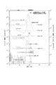
- FIG. 4 is a diagram showing the results of measuring the contents of oxygen, carbon, hydrogen, and fluorine contained in gallium nitride layers shown in Examples by secondary ion mass spectrometry.
- a member or region when a member or region is “above (or below)” another member or region, it means directly above (or directly below) the other member or region unless otherwise specified. Includes not only one case but also the case above (or below) another member or region, that is, the case where another component is included between above (or below) another member or region .
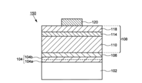
- FIG. 1 shows an example of the structure of a laminated structure 100 according to an embodiment of the present invention.
- the laminated structure 100 includes an amorphous substrate 102 , a buffer layer 106 provided on the amorphous substrate 102 , and a gallium nitride based semiconductor layer 108 provided on the buffer layer 106 .
- the laminated structure 100 may include a base insulating layer 104 between the amorphous substrate 102 and the buffer layer 106 .
- the amorphous substrate 102 preferably has a low thermal expansion coefficient, a high strain point, and a high surface flatness.
- the amorphous substrate 102 preferably has an expansion coefficient of less than 50 ⁇ 10 ⁇ 7 /° C. and a strain point of 600° C. or higher.
- the amorphous substrate 102 in this embodiment only needs to have heat resistance of about 700° C., and is not required to have heat resistance of 1000° C. or more like a sapphire substrate.
- the amorphous substrate 102 preferably contains 0.1% or less of an alkali metal such as sodium (Na).
- a glass substrate made of at least one kind of aluminoborosilicate glass and aluminosilicate glass can be used, and an alkali-free glass substrate is preferable.
- Such glass substrates are used in liquid crystal displays and organic electroluminescence (organic EL) displays, and large-area glass substrates called mother glass are provided on the market.
- organic EL organic electroluminescence
- mother glass large-area glass substrates called mother glass are provided on the market.
- amorphous substrate 102 it is also possible to use a flexible resin substrate such as a polyimide substrate, an acrylic substrate, a siloxane substrate, or a fluorine resin substrate.
- a quartz glass substrate can also be used as the amorphous substrate 102 .
- a base insulating layer 104 may be provided on the amorphous substrate 102 .
- the base insulating layer 104 is formed using an inorganic insulating film.
- As the inorganic insulating film a silicon nitride film, a silicon oxide film, a silicon oxynitride film, an aluminum nitride film, an aluminum oxide film, an aluminum oxynitride film, or the like can be used.
- the base insulating layer 104 has a single-layer structure of these inorganic insulating films or a laminated structure of a plurality of inorganic insulating films.
- FIG. 1 shows the case where the base insulating layer 104 has a laminated structure.
- FIG. 1 shows an example in which the base insulating layer 104 is formed of a silicon nitride layer 104a provided in contact with the amorphous substrate 102 and a silicon oxide layer 104b provided thereon.
- the silicon nitride layer 104a has the effect of preventing impurities contained in the amorphous substrate 102 from diffusing into the buffer layer 106 and the gallium nitride based semiconductor layer 108.
- a particularly problematic impurity is an alkali metal such as sodium contained in the amorphous substrate 102 in a trace amount. If the silicon nitride layer 104a has a film thickness of 20 nm or more, the diffusion of alkali metal can be prevented.
- the film thickness of the silicon nitride layer 104a can be, for example, 20 nm or more and 500 nm or less, preferably 100 nm or more and 300 nm or less, and can be formed with a film thickness of 150 nm, for example.
- the silicon oxide layer 104b can improve adhesion of the buffer layer 106 and prevent peeling.
- the silicon oxide layer 104b preferably has a thickness of 20 nm or more.
- the thickness of the silicon oxide layer 104b can be, for example, 20 nm or more and 500 nm or less, preferably 50 nm or more and 200 nm or less, and can be formed with a thickness of 100 nm, for example.
- the gallium nitride-based semiconductor layer 108 By providing the underlying insulating layer 104 on the amorphous substrate 102, diffusion of impurities into the gallium nitride based semiconductor layer 108 can be prevented, and high purity can be achieved. Thereby, the gallium nitride-based semiconductor layer 108 with high crystallinity can be formed.
- Buffer Layer A buffer layer 106 is provided over the amorphous substrate 102 .
- the buffer layer 106 preferably has crystallinity, that is, at least one of a crystalline metal and a metal compound. Crystals of the buffer layer 106 have an orientation, and the orientation is preferably c-axis orientation.
- the buffer layer 106 is preferably a crystal having rotational symmetry, for example, the crystal surface preferably has six-fold symmetry.
- the buffer layer 106 preferably has a hexagonal close-packed structure, a face-centered cubic structure, or a structure conforming to these.
- the structure conforming to the hexagonal close-packed structure or the face-centered cubic structure includes a crystal structure in which the c-axis is not 90 degrees with respect to the a-axis and the b-axis.
- the buffer layer 106 using a conductive material having a hexagonal close-packed structure or a similar structure is oriented in the (0001) direction, that is, in the c-axis direction with respect to the amorphous substrate 102 (hereinafter referred to as hexagonal close-packed structure). (0001) orientation of the dense structure is preferred.
- the buffer layer 106 having a face-centered cubic structure or a structure similar thereto is oriented in the (111) direction with respect to the amorphous substrate 102 (hereinafter referred to as the (111) orientation of the face-centered cubic structure). is preferred.
- the buffer layer 106 is provided between the amorphous substrate 102 and the gallium nitride based semiconductor layer 108 . Since the gallium nitride-based semiconductor layer 108 having crystallinity is formed on the amorphous substrate 102, the buffer layer 106 functions as a buffer layer that alleviates lattice mismatch. Crystallization of the gallium nitride based semiconductor layer 108 can be achieved by the buffer layer 106 having the above crystallinity.
- the buffer layer 106 has a c-axis orientation and has a crystalline surface having six-fold rotational symmetry such as a hexagonal close-packed structure or a face-centered cubic structure, so that the c-axis of the gallium nitride-based semiconductor layer 108 is Orientation can be controlled so as to grow in the film thickness direction.
- the buffer layer 106 preferably has a flat surface.
- the flatness of the surface of the buffer layer 106 is represented by arithmetic mean roughness (Ra), the value is preferably less than 2.5 nm, more preferably less than 2.3 nm.
- the flat surface of the buffer layer 106 can improve the crystallinity of the gallium nitride based semiconductor layer 108 . It is preferable that the Ra of the buffer layer 106 is as small as possible.
- the surface roughness of the buffer layer 106 can be measured with an atomic force microscope (AFM).
- the buffer layer 106 is preferably a thin film while having crystallinity.
- the thickness of the buffer layer 106 is not particularly limited as long as it can be regarded as a thin film. However, if the film thickness is too thin, the flatness of the surface may be poor and the film may not have crystallinity. On the other hand, if the film thickness of the buffer layer 106 is excessively large, crystallization causes a surface morphology peculiar to metal, resulting in deterioration of the flatness of the surface. Therefore, the film thickness of the buffer layer 106 is preferably 5 nm or more and 500 nm or less, more preferably 10 nm or more and 200 nm or less.
- the film thickness of the buffer layer 106 can be measured by a contact-type profilometer or an optical film-thickness meter (ellipsometry), or by a scanning electron microscope (SEM) or a transmission electron microscope (TEM). It can be measured from the image obtained.
- the buffer layer 106 can be made of metal. Titanium (Ti) and aluminum (Al) are preferably used as the metal material for forming the buffer layer 106. In addition, silver (Ag), nickel (Ni), copper (Cu), strontium (Sr), rhodium ( Rh), palladium (Pd), iridium (Ir), platinum (Pt), gold (Au), and the like can be used. In addition, the buffer layer 106 can also use metal oxide materials such as zinc oxide (ZnO) and titanium dioxide (TiO 2 ).
- Such a buffer layer 106 can be produced by a sputtering method or an electron beam vacuum deposition method.
- the buffer layer 106 can be formed of an insulating layer instead of a metal layer. That is, the buffer layer 106 can also be formed using an insulating material.
- the insulating buffer layer 106 aluminum nitride (AlN), aluminum oxide ( Al2O3 ), or the like can be used.
- the insulating buffer layer 106 preferably has the same crystallinity as described above and preferably has the same film thickness.
- the gallium nitride based semiconductor layer 108 includes at least one gallium nitride (GaN) layer.
- the gallium nitride-based semiconductor layer 108 is a single-layer gallium nitride layer.
- the gallium nitride-based semiconductor layer 108 includes a gallium nitride layer, and further includes at least one layer selected from an indium gallium nitride (InGaN) layer and an aluminum gallium nitride (AlGaN) layer, and these layers are laminated. have a structure.
- the gallium nitride layer, the indium gallium nitride layer, and the aluminum gallium nitride layer forming the gallium nitride-based semiconductor layer 108 preferably have a stoichiometric composition. good too.
- the gallium nitride based semiconductor layer 108 preferably has crystallinity. That is, the gallium nitride layer forming the gallium nitride based semiconductor layer 108 preferably has crystallinity.
- the gallium nitride layer is preferably monocrystalline, but may be polycrystalline, microcrystalline, or nanocrystalline.
- the crystal structure of the gallium nitride layer preferably has a wurtzite structure.
- the gallium nitride layer forming the gallium nitride based semiconductor layer 108 preferably has c-axis orientation or (111) orientation.
- the conductivity type of the gallium nitride layer forming part or all of the gallium nitride based semiconductor layer 108 may be substantially intrinsic, or may be n-type or p-type conductivity. good too.
- the gallium nitride layer may contain dopants for valence electron control.
- the n-type gallium nitride layer may be doped with one element selected from silicon (Si) and germanium (Ge) as a dopant.
- the p-type gallium nitride layer may be doped with an element selected from magnesium (Mg), zinc (Zn), cadmium (Cd), and beryllium (Be) as a dopant.
- the n-type gallium nitride layer preferably has a carrier concentration of 1 ⁇ 10 18 /cm 3 or more.
- the p-type gallium nitride layer preferably has a carrier concentration of 5 ⁇ 10 16 /cm 3 or more.
- the substantially intrinsic (in other words, highly resistive) gallium nitride layer may contain zinc (Zn) as a dopant.
- a gallium nitride layer forming part or all of the gallium nitride-based semiconductor layer 108 is provided in contact with the buffer layer 106 .
- a gallium nitride layer is deposited over the buffer layer 106 .
- a gallium nitride layer having a c-axis orientation or (111) orientation is formed.
- the gallium nitride layer may have an amorphous structure near the interface with the buffer layer 106, but preferably has crystallinity in a region (bulk) away from the interface.
- the gallium nitride layer forming part or all of the gallium nitride based semiconductor layer 108 has crystallinity, the performance of the gallium nitride based semiconductor device can be improved.
- the gallium nitride-based semiconductor device is a light-emitting device, it can increase the emission intensity, and if it is an active device such as a transistor, it can increase the carrier mobility.
- the gallium nitride layer forming part or all of the gallium nitride based semiconductor layer 108 contains oxygen (O), carbon (C), hydrogen (H), Fluorine (F) may be included.
- the concentration of oxygen contained in the gallium nitride layer is preferably 2 ⁇ 10 21 /cm 3 or less, more preferably 1 ⁇ 10 21 /cm 3 or less.
- the concentration of carbon contained in the gallium nitride layer is preferably 5 ⁇ 10 19 /cm 3 or less, more preferably 3 ⁇ 10 19 /cm 3 or less.
- the concentration of hydrogen contained in the gallium nitride layer is preferably 3 ⁇ 10 20 /cm 3 or less, more preferably 2 ⁇ 10 20 /cm 3 or less.
- the concentration of fluorine contained in the gallium nitride layer is preferably 1 ⁇ 10 19 /cm 3 or less, more preferably 5 ⁇ 10 17 /cm 3 or less.
- the lower limit values of oxygen (O), carbon (C), hydrogen (H), and fluorine (F) as impurity elements are not limited from the viewpoint of achieving high purity of the gallium nitride layer, and are preferably as low as possible. However, the lower limit may be equal to or higher than the detection limit of the measuring device for detecting these impurity elements.
- the background level shall be equal to or higher than the background level. can do.
- the lower limits are 6 ⁇ 10 16 /cm 3 or more for oxygen (O), 4 ⁇ 10 16 /cm 3 or more for carbon (C), 2 ⁇ 10 17 /cm 3 or more for hydrogen (H), and 2 ⁇ 10 17 /cm 3 or more for fluorine ( F) can be 2 ⁇ 10 15 /cm 3 or more.
- a high impurity concentration in the gallium nitride layer is not preferable because the crystallinity is lowered and the defect level that becomes a carrier trap increases.
- Oxygen contained in the gallium nitride layer acts as a dopant, so if the above range is exceeded, the conductivity may change, possibly degrading device characteristics.
- Hydrogen contained in the gallium nitride layer may passivate and inactivate the p-type dopant in particular, so it is preferable not to exceed the above range. Since carbon contained in the gallium nitride layer forms crystal defects and forms defect levels to lower the light emission efficiency, it is preferable not to exceed the above range.
- the concentrations of these impurity elements are based on measured values obtained by secondary ion mass spectrometry.
- the above impurity concentration is quantified based on the secondary ion intensity measured in the depth direction (thickness direction of the film) for each element using cesium ions (Cs + ) as primary ions. It is based on the value obtained by performing
- Impurities such as oxygen, hydrogen, carbon, and fluorine contained in the gallium nitride-based semiconductor layer 108 originate from impurities contained in the sputtering target material. Moreover, these impurity elements originate from the residual gas in the film forming chamber of the sputtering apparatus. Impurity elements contained in the gallium nitride layer are considered to be incorporated into the film from these sources during sputtering film formation. These impurity elements are different from impurities intentionally added for the purpose of controlling valence electrons, and can be said to be unavoidable impurities.
- the concentrations of oxygen, carbon, hydrogen, and fluorine that are inevitably contained in the gallium nitride layer forming part or all of the gallium nitride-based semiconductor layer 108 are highly purified so that they fall within the numerical ranges described above. , the crystallinity of the gallium nitride layer can be enhanced. Namely.
- the crystallinity of the gallium nitride-based semiconductor layer 108 provided on the amorphous substrate 102 is improved by improving the purity of the gallium nitride layer forming part or all of the gallium nitride-based semiconductor layer 108 . can increase
- Method for Producing Laminated Structure There is no particular limitation on the method for producing the laminated structure 100 according to the present embodiment. However, the laminated structure 100 according to this embodiment can be favorably produced according to the following production method.
- the laminated structure 100 is manufactured by a manufacturing method including a step of forming a buffer layer 106 on an amorphous substrate 102 and a step of forming a gallium nitride based semiconductor layer 108 on the buffer layer 106. can be made.
- a step of forming the base insulating layer 104 on the amorphous substrate 102 is included before forming the buffer layer 106 .
- the step of forming the gallium nitride-based semiconductor layer 108 includes a film formation step using a sputtering method. The following description includes the step of forming the base insulating layer 104 .
- a glass substrate is used as the amorphous substrate 102 .
- the glass substrate is a non-alkali glass substrate made of aluminoborosilicate glass, aluminosilicate glass, or the like.
- Amorphous substrate 102 is cleaned to form a clean surface.
- any cleaning method may be used, for example, cleaning is performed with a mixed cleaning solution containing sulfuric acid and hydrogen peroxide or hydrochloric acid and hydrogen peroxide, followed by ultrapure water rinsing to wash away the mixed cleaning solution.
- the base insulating layer 104 is formed of a silicon nitride layer 104a and a silicon oxide layer 104b. There is no limitation on the method for forming the silicon nitride layer 104a and the silicon oxide layer 104b.
- the silicon nitride layer 104a is formed by a plasma CVD (Chemical Vapor Deposition) method using reactive gases such as silane (SiH 4 ), ammonia (NH 3 ), and nitrogen (N 2 ), and the silicon oxide layer 104b is formed by It is produced by a plasma CVD method using raw material gases such as silane (SiH 4 ), nitrous oxide (N 2 O), tetraethyl orthosilicate (TEOS).
- the silicon nitride layer 104a and the silicon oxide layer 104b can be deposited continuously.
- the silicon nitride layer 104a may be formed by reactive sputtering using silicon as a sputtering target, and the silicon oxide layer 104b may be formed using quartz as a sputtering target.
- the silicon nitride layer 104a is formed with a thickness of 20 nm or more and 500 nm or less, preferably 100 nm or more and 300 nm or less, for example, 150 nm.
- the silicon oxide layer 104b is formed with a thickness of 20 nm to 500 nm, preferably 50 nm to 200 nm, for example, 100 nm.
- Buffer Layer A buffer layer 106 is formed over the base insulating layer 104 .
- the buffer layer 106 is produced by a sputtering method or a vacuum deposition method.
- a known sputtering method can be used as the sputtering method.
- Known techniques include DC sputtering, RF sputtering, AC sputtering, DC magnetron sputtering, RF magnetron sputtering, pulse sputtering, and ion beam sputtering, induced plasma assisted sputtering.
- DC magnetron sputtering method or RF magnetron sputtering method is preferably applied in order to uniformly form a film on a large glass substrate at high speed.
- the buffer layer 106 When fabricating the buffer layer 106 by sputtering, a metal target, an oxide target, or a nitride target is used as a sputtering target. Since the buffer layer 106 preferably has an orientation, the target material preferably has a high purity, and preferably has a purity of 5N (99.999%) or higher. Moreover, in order to suppress the generation of particles by preventing the occurrence of abnormal discharge, it is preferable to use a target material with a low defect density and a smooth surface.
- the buffer layer 106 When a metal buffer layer is formed as the buffer layer 106, it is preferable to use titanium (Ti) and aluminum (Al) as the metal material as described above, and silver (Ag), nickel (Ni), and copper. (Cu), strontium (Sr), rhodium (Rh), palladium (Pd), iridium (Ir), platinum (Pt), and gold (Au).
- the buffer layer 106 may be formed of a metal oxide such as zinc oxide (ZnO) or titanium dioxide (TiO 2 ) instead of metal.
- the buffer layer 106 may be formed of an insulating material such as aluminum nitride (AlN) or aluminum oxide (Al 2 O 3 ). The thickness of the buffer layer 106 is 5 nm to 500 nm, preferably 10 nm to 200 nm.
- the buffer layer 106 When the buffer layer 106 is made of metal, a high-purity metal is used as a sputtering target.
- a high-purity metal is used as a sputtering target.
- a metal oxide When the buffer layer 106 is formed of a metal oxide, a sintered body of metal oxide is used as a sputtering target.
- a sintered body of an insulating material is used as a sputtering target.
- These target materials are used by being brazed to a backing plate made of copper (Cu), aluminum (Al), stainless steel, or the like.
- the backing plate may be integrally formed.
- the buffer layer 106 is formed by a sputtering method
- the ultimate vacuum of the film formation chamber of the sputtering apparatus is 1 ⁇ 10 ⁇ 4 Pa or less.
- the substrate it is preferable to heat the substrate to 100.degree. C. to 300.degree.
- the gallium nitride based semiconductor layer 108 is produced by a sputtering method.
- a gallium nitride-based sintered body is used as a sputtering target.
- a gallium nitride layer is formed as the gallium nitride-based semiconductor layer 108
- a gallium nitride sintered body is used as the target material of the sputtering target. From the viewpoint of enhancing the crystallinity of the gallium nitride layer, it is preferable that the amount of oxygen contained in the sputtering target material is as low as possible.
- the oxygen content of the gallium nitride sintered body used as the target material is preferably 3 atomic % or less, more preferably 1 atomic % or less.
- the content of metal impurities other than gallium is preferably less than 0.1 at %, more preferably less than 0.01 at %.
- the target material made of the gallium nitride sintered body preferably has a resistivity of 1 ⁇ 10 2 ⁇ cm or less and a density of 3.0 g/cm 3 or more and 5.4 g/cm 3 or less. No precipitation is preferred.
- the area of the sputtering target is preferably 18 cm 2 or more, more preferably 100 cm 2 or more.
- a DC sputtering method As a sputtering method, a DC sputtering method, an RF sputtering method, an AC sputtering method, a DC magnetron sputtering method, an RF magnetron sputtering method, a pulse sputtering method, an ion beam sputtering method, and an induced plasma-assisted sputtering method can be used.
- the DC magnetron sputtering method and the RF magnetron sputtering method are preferable because they can cope with an increase in the area of the amorphous substrate 102 .
- it is preferable to employ a moving magnet method which enables the entire surface of the sputtering target to be eroded, thereby enabling effective use of materials.
- the gas pressure during film formation of the gallium nitride layer by sputtering is less than 0.3 Pa, preferably 0.1 Pa or less, and more preferably 0.08 Pa or less.
- the lower the gas pressure during sputtering film formation the more the sputtered particles adhering to the deposition surface can be diffused, and the crystallinity can be improved.
- the ultimate vacuum of the film formation chamber of the sputtering apparatus is preferably 3 ⁇ 10 ⁇ 5 Pa or less, more preferably 1 ⁇ 10 ⁇ 5 Pa or less.
- the amorphous substrate 102 (that is, the surface of the buffer layer 106 that becomes the deposition surface) is preferably reverse-sputtered.
- Reverse sputtering is a method of cleaning the surface by irradiating the amorphous substrate 102 side with rare gas ions such as argon (Ar) instead of the sputtering target side.
- Ar argon
- the sputtering apparatus is preferably provided with a dedicated processing chamber for performing reverse sputtering in addition to the film forming chamber. It is possible to form a film while maintaining the cleanliness of the surface of the substrate 102 (that is, the surface of the buffer layer 106 serving as the deposition surface).
- the substrate temperature (also referred to as “film formation temperature”) during sputtering film formation is preferably room temperature to 600° C. or lower, more preferably 100° C. or higher and 400° C. or lower. In addition, if the temperature is higher than 600° C., the heat resistance temperature of the amorphous substrate 102 is exceeded, and the cost of the sputtering apparatus becomes high, reducing the advantage of using the sputtering method.
- the substrate temperature may be room temperature (including the case where the substrate is not intentionally heated) or higher. The crystallinity of the gallium nitride layer deposited on layer 106 can be improved.
- a rare gas such as argon (Ar) is usually used as a gas for sputtering (sputtering gas), but nitrogen (N 2 ) gas is preferably used in forming a gallium nitride film.
- nitrogen gas is usually used as the sputtering gas, generation of nitrogen defects can be suppressed.
- the power density during discharge is preferably 5 W/cm 2 or less, more preferably 2.5 W/cm 2 or less, and even more preferably 1.5 W/cm 2 or less.
- the lower limit is preferably 0.1 W/cm 2 or more, more preferably 0.3 W/cm 2 or more.
- the power density is calculated by dividing the power applied during discharge by the area of the sputtering target material. If the electric power during discharge is higher than 5 W/cm 2 , coarse polycrystalline particles tend to peel off from the sputtering target. If the power density is less than 0.1 W/cm 2 , the discharge becomes stable and the film formation speed decreases, resulting in a decrease in film productivity.
- the film thickness of the gallium nitride layer is preferably 30 nm or more, more preferably 50 nm or more. With such a film thickness, a gallium nitride layer having crystallinity can be formed on the buffer layer 106 . Further, the film thickness of the gallium nitride layer may be 5000 nm or less, preferably 1000 nm or less, more preferably 200 nm to 500 nm or less.
- the gallium nitride-based semiconductor layer 108 is a gallium nitride layer, but by changing the material of the sputtering target, an indium gallium nitride (InGaN) layer and an aluminum gallium nitride (AlGaN) layer can be obtained. Crystalline thin films with different compositions, such as layers, can be fabricated.
- a gallium nitride-based semiconductor layer 108 in which a plurality of layers with different compositions are stacked can be formed by mounting sputtering targets with different compositions in each film formation chamber. can.
- the concentration of impurities such as oxygen contained in the sputtering target material is reduced, high vacuum evacuation is performed during the sputtering film formation, and a process such as reverse sputtering is performed.
- the gallium nitride-based semiconductor layer 108 with low concentration of impurities such as oxygen, carbon, hydrogen, and fluorine and high crystallinity can be produced.
- the oxygen concentration is 2 ⁇ 10 21 /cm 3 or less, preferably 1 ⁇ 10 21 /cm 3 or less
- the carbon concentration is 5 ⁇ 10 19 /cm 3 or less, preferably 3 ⁇ 10 19 /cm 3 or less
- the hydrogen concentration is 3 ⁇ 10 20 /cm 3 or less, preferably 2 ⁇ 10 20 /cm 3 or less
- the fluorine concentration is 1 ⁇ 10 19 /cm 3 or less, preferably 5 ⁇ 10 17 /cm 3 or less. It is possible to fabricate a gallium nitride layer with With such an impurity concentration, the laminated structure 100 in which the crystalline gallium nitride based semiconductor layer 108 is formed on the amorphous substrate 102 can be produced.
- the gallium nitride-based semiconductor layer 108 uses a sputtering target made of gallium nitride with reduced impurities such as oxygen, and the amorphous substrate 102 is subjected to a process such as reverse sputtering. After being evacuated to a high vacuum, it is produced by the sputtering method at the predetermined power density.
- the concentration of impurities such as oxygen, carbon, and hydrogen is reduced, and the gallium nitride based semiconductor layer 108 with high crystallinity and low defect density can be obtained.
- Gallium Nitride-Based Semiconductor Device such as light-emitting devices and transistors can be manufactured from the laminated structure 100 according to the present embodiment.
- An example of a device having the laminated structure 100 as a basic structure is shown below. Note that the device shown below is an example, and the device realized by the laminated structure 100 is not limited to the illustrated structure.
- FIG. 2A shows a light emitting device 150 as an example of a gallium nitride based semiconductor device.
- the light-emitting device 150 has a laminated structure 100 in which a base insulating layer 104 , a buffer layer 106 and a gallium nitride based semiconductor layer 108 are laminated on an amorphous substrate 102 .
- the gallium nitride based semiconductor layer 108 has a structure in which an n-type gallium nitride layer 110, a light emitting layer 114, and a p-type gallium nitride layer 118 are laminated.
- An upper electrode layer 120 is provided on the p-type gallium nitride layer 118 .
- the upper electrode layer 120 is formed of a metal material such as gold (Au), a titanium (Ti)-gold (Au) alloy, or a transparent conductive film such as indium tin oxide (ITO).
- the structure of the light emitting layer 114 may vary, and may be formed by quantum well layers in which gallium nitride (GaN) layers and indium gallium nitride (InGaN) layers are alternately stacked.
- FIG. 2B shows a light-emitting device 155 in which the configuration of the gallium nitride-based semiconductor layer 108 is different from that in FIG. 2A.
- the light-emitting device 155 has a structure in which an n-type gallium nitride layer 110, an n-type aluminum gallium nitride layer 112, an indium gallium nitride layer 114 as a light-emitting layer, a p-type aluminum gallium nitride layer 116, and a p-type gallium nitride layer 118 are laminated. have. Since each of these layers has a different composition, they are formed using a sputtering target corresponding to each composition.
- the light-emitting device 150 shown in FIG. 2A and the light-emitting device 155 shown in FIG. 2B include the structure of the laminated structure 100 shown in this embodiment.
- the laminated structure 100 has a gallium nitride-based semiconductor layer 108 having a reduced concentration of impurities such as oxygen, carbon, and hydrogen and having high crystallinity on an amorphous substrate 102 . Since the gallium nitride-based semiconductor layer 108 can be formed on a large-area amorphous substrate 102, the number of light-emitting devices that can be separated from one amorphous substrate 102 can be increased. Productivity can be improved. Also, an LED array can be produced by arranging light emitting devices on the amorphous substrate 102, and a display device can be produced from the LED array.
- Transistor FIG. 3 shows a transistor 160 as an example of a gallium nitride based semiconductor device.
- Transistor 160 includes gallium nitride based semiconductor layer 108 formed on amorphous substrate 102 .
- the gallium nitride-based semiconductor layer 108 has a structure in which an n + -type gallium nitride layer 122, an n-type gallium nitride layer 124, a p-type gallium nitride layer 126, and an n-type gallium nitride layer 128 are laminated.
- the gate electrode 132 is provided so as to be embedded in the p-type gallium nitride layer 126 with the gate insulating layer 130 interposed therebetween.
- a source electrode 134 is provided on the n-type gallium nitride layer 128 .
- the buffer layer 106 may also function as the drain electrode. That is, by forming the buffer layer 106 using a metal or a conductive metal oxide, it can also function as a drain electrode.
- the transistor 160 shown in FIG. 3 can be used, for example, as a power transistor.
- the active layer of the transistor 160 is formed by the gallium nitride-based semiconductor layer 108 provided on the amorphous substrate 102 .
- the gallium nitride-based semiconductor layer 108 has high crystallinity with a reduced concentration of impurities such as oxygen, carbon, and hydrogen, and a reduced defect density. can be provided in
- a non-alkali glass substrate was used as the amorphous substrate 102 .
- a silicon nitride layer 104a with a thickness of 150 nm and a silicon oxide layer 104b with a thickness of 100 nm were formed on a non-alkali glass substrate.
- the silicon nitride layer 104a and the silicon oxide layer 104b were formed by plasma CVD.
- the silicon nitride layer 104a was formed using silane (SiH 4 ), ammonia (NH 3 ), and nitrogen (N 2 ) as reaction gases at an RF power density of 0.24 W/cm 2 and a substrate temperature of 400°C.
- the silicon oxide layer 104b was formed using silane (SiH 4 ) and nitrous oxide (N 2 O) as reaction gases at an RF power density of 0.61 W/cm 2 and a substrate temperature of 380°C.
- a titanium (Ti) layer having a thickness of 50 nm was formed as a buffer layer 106 on the underlying insulating layer 104 .
- the titanium (Ti) layer was formed by a sputtering method using a titanium (Ti) target at room temperature without heating the substrate.
- a gallium nitride layer was formed as the gallium nitride-based semiconductor layer 108 by a sputtering method.
- Sputtering conditions are as follows.
- Discharge method RF sputtering Film forming device: Magnetron sputtering device
- Target material Gallium nitride (oxygen content 7 atm%)
- Target size 120mm ⁇
- Target-substrate distance 150mm
- Deposition pressure 0.3 Pa
- Introduced gas Nitrogen Discharge power: 100W Film formation temperature: 200°C Film thickness: 100 nm Heat treatment temperature: 600°C
- the impurity concentration of the gallium nitride layer produced under the above conditions was evaluated by secondary ion mass spectrometry. As impurities contained in the gallium nitride layer, concentrations of oxygen, hydrogen, carbon, and fluorine were measured.
- Measuring device PHI ADEPT1010
- Primary ion species Cs + Primary acceleration voltage: 2.0 kV
- Detection area 90 ⁇ m ⁇ 90 ⁇ m
- FIG. 4 shows a graph showing the distribution in the depth direction of each element of oxygen, hydrogen, carbon, and fluorine contained in the gallium nitride layer measured by secondary ion mass spectrometry.
- the horizontal axis indicates the depth from the surface of the gallium nitride film, and the vertical axis indicates the concentration converted from the secondary ion intensity of each element.
- the graph shown in FIG. 4 shows the Back-Geland level (detection limit) of each element of oxygen, hydrogen, carbon, and fluorine.
- the background is 6.0 ⁇ 10 16 /cm 3 oxygen, 2.1 ⁇ 10 17 /cm 3 hydrogen, 4.5 ⁇ 10 16 /cm 3 carbon, and 1.9 ⁇ 10 15 /cm fluorine. 3 .
- the graph shown in FIG. 4 also shows the secondary ion intensities of gallium (Ga)+nitrogen (N), gallium (Ga), and titanium (Ti) as matrix markers.
- the part where the secondary ion intensity of gallium (Ga) + nitrogen (N) and gallium (Ga) is flat, which is shown as a matrix marker, is the gallium nitride layer. range. From the graph of FIG. 4, it can be seen that the gallium nitride layer extends from the surface to about 80 ⁇ m, and the titanium layer as the buffer layer exists after that. Quantitative values of oxygen, hydrogen, carbon, and fluorine can be read from the area where the matrix marker is flat. Due to the characteristics of secondary ion mass spectrometry, profile pile-up is observed near the film surface and near the interface due to charge-up and impurity contamination, so these portions should not be taken into consideration.
- Table 1 shows the respective concentrations of oxygen, hydrogen, carbon, and fluorine contained in the gallium nitride layer read from the graph shown in FIG.
- the gallium nitride layer produced in this example had a hydrogen concentration of 9.7 ⁇ 10 19 /cm 3 , a carbon concentration of 1.4 ⁇ 10 19 /cm 3 , and an oxygen concentration of 7.7 ⁇ 10 19 /cm 3 .
- 1 ⁇ 10 20 /cm 3 and a fluorine concentration of 1.9 ⁇ 10 17 /cm 3 were obtained.
- the profile of hydrogen shows a tendency to gradually decrease from the surface to the inside of the gallium nitride layer, but when reading quantitative values, the values near the center of the film are read.
- impurities that are inevitably introduced when a gallium nitride film is formed by a sputtering method are reduced as much as possible even when an amorphous substrate such as a glass substrate is used. shows that a gallium nitride layer with excellent crystallinity can be produced even when an amorphous substrate is used.
- 100 laminated structure, 102: amorphous substrate, 104: underlying insulating layer, 106: buffer layer, 108: gallium nitride based semiconductor layer, 110: n-type gallium nitride layer, 112: n-type aluminum gallium nitride layer, 114 : light emitting layer, 115: indium gallium nitride layer, 116: p-type aluminum gallium nitride layer, 118: p-type gallium nitride layer, 120: upper electrode layer, 122: n + type gallium nitride layer, 124: n-type gallium nitride layer, 126: p-type gallium nitride layer, 128: n-type gallium nitride layer, 130: gate insulating layer, 132: gate electrode, 134: source electrode, 150: light emitting device, 155: light emitting device, 160: transistor
Abstract
A multilayer structure comprising an amorphous substrate, a buffer layered formed on the amorphous substrate, and one or more gallium-nitride-based semiconductor layers formed on the buffer layer, wherein the gallium-nitride-based semiconductor layers include at least one gallium nitride layer, the gallium nitride layer having an oxygen concentration of 1×10²¹ /cm3 or less. The gallium nitride layer has a carbon concentration of 3×10¹⁹ /cm3 or less, a hydrogen concentration of 2×10²⁰ /cm3 or less, and a fluorine concentration of 5×10¹⁷ /cm3 or less.
Description
本発明の一実施形態は、非晶質基板上に形成された窒化ガリウム系半導体層を含む積層構造体、その積層構造体により構成される窒化ガリウム系半導体デバイスに関する。
One embodiment of the present invention relates to a laminated structure including a gallium nitride based semiconductor layer formed on an amorphous substrate, and a gallium nitride based semiconductor device constituted by the laminated structure.
窒化ガリウムは発光ダイオードに使用され、次世代半導体素材としてパワートランジスタ、集積回路への用途が期待されている。窒化ガリウムは有機金属気相成長(MOCVD:Metal Organic Chemical Vapor Deposition)法で製造されている。MOCVD法で窒化ガリウムの成長には1000℃以上に基板を加熱する必要があるため、デバイスの製造に必要とされる消費電力が莫大であることが問題とされている。そこで、低温でも成膜が可能なスパッタリング法を用いて結晶性を有する窒化ガリウム膜を作製する技術の開発が行われている。例えば、窒化ガリウムのスパッタリングターゲットを用い、単結晶シリコン基板やサファイア基板の上に結晶性を有する窒化ガリウム層を成膜する方法が開示されている(特許文献1乃至3参照)。
Gallium nitride is used in light-emitting diodes, and is expected to be used in power transistors and integrated circuits as a next-generation semiconductor material. Gallium nitride is manufactured by a metal organic chemical vapor deposition (MOCVD) method. Since the substrate must be heated to 1000° C. or more to grow gallium nitride by the MOCVD method, the problem is that the power consumption required for device manufacture is enormous. Therefore, a technique for forming a gallium nitride film having crystallinity using a sputtering method capable of forming a film even at a low temperature has been developed. For example, a method of forming a crystalline gallium nitride layer on a single crystal silicon substrate or a sapphire substrate using a gallium nitride sputtering target has been disclosed (see Patent Documents 1 to 3).
窒化ガリウム膜の成長には、サファイア基板や単結晶シリコン基板などの結晶性を有する基板が用いられている。しかし、サファイア基板や単結晶シリコン基板は、価格が高く、基板サイズの大型化が難しいという問題がある。窒化ガリウム膜を形成する基板として、液晶ディスプレイで用いられているようなガラス基板に代表される非晶質基板を用いることができれば、基板のコストを削減することができ、大面積化も容易となる。しかし、これまでのところガラス基板のような非晶質基板の上に結晶性を有し、高品質の窒化ガリウムを作製した例は報告されていない。
Crystalline substrates such as sapphire substrates and single-crystal silicon substrates are used to grow gallium nitride films. However, the sapphire substrate and the single-crystal silicon substrate are expensive, and there is a problem that it is difficult to increase the size of the substrate. If an amorphous substrate, typified by the glass substrate used in liquid crystal displays, can be used as the substrate on which the gallium nitride film is formed, the cost of the substrate can be reduced and the area can be easily increased. Become. However, so far, there have been no reports of producing high-quality gallium nitride having crystallinity on an amorphous substrate such as a glass substrate.
本発明の一実施形態は、このような課題に鑑み、基板価格が安い非晶質基板上に、スパッタリング法により結晶性の優れた窒化ガリウム系半導体層を含む積層構造体を提供することを目的の一つとする。
In view of such problems, an object of one embodiment of the present invention is to provide a laminated structure including a gallium nitride-based semiconductor layer having excellent crystallinity by a sputtering method on an amorphous substrate whose substrate price is low. be one of
本発明の一実施形態に係る積層構造体は、非晶質基板と、非晶質基板上のバッファ層と、バッファ層上の窒化ガリウム系半導体層と、を有し、窒化ガリウム系半導体層は少なくとも1層の窒化ガリウム層を含み、窒化ガリウム層の酸素濃度が1×10²¹/cm3以下である。
A laminated structure according to one embodiment of the present invention has an amorphous substrate, a buffer layer on the amorphous substrate, and a gallium nitride-based semiconductor layer on the buffer layer, wherein the gallium nitride-based semiconductor layer is At least one gallium nitride layer is included, and the gallium nitride layer has an oxygen concentration of 1×10 21 /cm 3 or less.
以下、本発明の実施の形態を、図面等を参照しながら説明する。但し、本発明は多くの異なる態様で実施することが可能であり、以下に例示する実施の形態の記載内容に限定して解釈されるものではない。図面は説明をより明確にするため、実際の態様に比べ、各部の幅、厚さ、形状等について模式的に表される場合があるが、あくまで一例であって、本発明の解釈を限定するものではない。また、本明細書と各図において、既出の図に関して前述したものと同様の要素には、同一の符号(又は数字の後にa、bなどを付した符号)を付して、詳細な説明を適宜省略することがある。さらに各要素に対する「第1」、「第2」と付記された文字は、各要素を区別するために用いられる便宜的な標識であり、特段の説明がない限りそれ以上の意味を有しない。
Hereinafter, embodiments of the present invention will be described with reference to the drawings. However, the present invention can be implemented in many different aspects and should not be construed as being limited to the description of the embodiments exemplified below. In order to make the description clearer, the drawings may schematically show the width, thickness, shape, etc. of each part compared to the actual embodiment, but this is only an example and limits the interpretation of the present invention. not a thing In addition, in this specification and each figure, the same reference numerals (or numerals followed by a, b, etc.) are attached to the same elements as those described above with respect to the previous figures, and a detailed description is given. It may be omitted as appropriate. Further, the letters "first" and "second" for each element are convenient labels used to distinguish each element and have no further meaning unless otherwise specified.
本明細書において、ある部材又は領域が他の部材又は領域の「上に(又は下に)」あるとする場合、特段の限定がない限りこれは他の部材又は領域の直上(又は直下)にある場合のみでなく他の部材又は領域の上方(又は下方)にある場合を含み、すなわち、他の部材又は領域の上方(又は下方)において間に別の構成要素が含まれている場合も含む。
In this specification, when a member or region is “above (or below)” another member or region, it means directly above (or directly below) the other member or region unless otherwise specified. Includes not only one case but also the case above (or below) another member or region, that is, the case where another component is included between above (or below) another member or region .
1.積層構造体
図1は、本発明の一実施形態に係る積層構造体100の構造の一例を示す。積層構造体100は、非晶質基板102、非晶質基板102の上に設けられたバッファ層106、及びバッファ層106の上に設けられた窒化ガリウム系半導体層108を含む。積層構造体100は、非晶質基板102とバッファ層106との間に下地絶縁層104が設けられていてもよい。 1. Laminated Structure FIG. 1 shows an example of the structure of a laminatedstructure 100 according to an embodiment of the present invention. The laminated structure 100 includes an amorphous substrate 102 , a buffer layer 106 provided on the amorphous substrate 102 , and a gallium nitride based semiconductor layer 108 provided on the buffer layer 106 . The laminated structure 100 may include a base insulating layer 104 between the amorphous substrate 102 and the buffer layer 106 .
図1は、本発明の一実施形態に係る積層構造体100の構造の一例を示す。積層構造体100は、非晶質基板102、非晶質基板102の上に設けられたバッファ層106、及びバッファ層106の上に設けられた窒化ガリウム系半導体層108を含む。積層構造体100は、非晶質基板102とバッファ層106との間に下地絶縁層104が設けられていてもよい。 1. Laminated Structure FIG. 1 shows an example of the structure of a laminated
1-1.非晶質基板
非晶質基板102は、熱膨張係数が低く、歪み点が高く、表面の平坦性が高いことが好ましい。例えば、非晶質基板102は、膨張係数が50×10-7/℃より小さく、歪み点が600℃以上であることが好ましい。本実施形態における非晶質基板102は、700℃程度の耐熱性があればよく、サファイア基板のような1000℃以上の耐熱性が要求されるものではない。また、非晶質基板102は、ナトリウム(Na)のようなアルカリ金属の含有量が0.1%以下であることが好ましい。 1-1. Amorphous Substrate Theamorphous substrate 102 preferably has a low thermal expansion coefficient, a high strain point, and a high surface flatness. For example, the amorphous substrate 102 preferably has an expansion coefficient of less than 50×10 −7 /° C. and a strain point of 600° C. or higher. The amorphous substrate 102 in this embodiment only needs to have heat resistance of about 700° C., and is not required to have heat resistance of 1000° C. or more like a sapphire substrate. In addition, the amorphous substrate 102 preferably contains 0.1% or less of an alkali metal such as sodium (Na).
非晶質基板102は、熱膨張係数が低く、歪み点が高く、表面の平坦性が高いことが好ましい。例えば、非晶質基板102は、膨張係数が50×10-7/℃より小さく、歪み点が600℃以上であることが好ましい。本実施形態における非晶質基板102は、700℃程度の耐熱性があればよく、サファイア基板のような1000℃以上の耐熱性が要求されるものではない。また、非晶質基板102は、ナトリウム(Na)のようなアルカリ金属の含有量が0.1%以下であることが好ましい。 1-1. Amorphous Substrate The
このような特性を満たす非晶質基板102として、例えば、アルミノホウケイ酸ガラス、及び、アルミノシリケートガラスの少なくとも一種からなるガラス基板を用いることができ、無アルカリガラス基板であることが好ましい。このようなガラス基板は、液晶ディスプレイ、有機エレクトロルミネセンス(有機EL)ディスプレイに使用されており、マザーガラスと呼ばれる大面積ガラス基板が市場に提供されている。非晶質基板102としてガラス基板を用いることで、大面積ガラス基板の上に窒化ガリウム系半導体層108を形成することができる。
As the amorphous substrate 102 satisfying such characteristics, for example, a glass substrate made of at least one kind of aluminoborosilicate glass and aluminosilicate glass can be used, and an alkali-free glass substrate is preferable. Such glass substrates are used in liquid crystal displays and organic electroluminescence (organic EL) displays, and large-area glass substrates called mother glass are provided on the market. By using a glass substrate as the amorphous substrate 102, the gallium nitride based semiconductor layer 108 can be formed on the large glass substrate.
非晶質基板102として、ポリイミド基板、アクリル基板、シロキサン基板、フッ素樹脂基板などの可撓性を有する樹脂基板を用いることも可能である。また、非晶質基板102として、石英ガラス基板を用いることもできる。
As the amorphous substrate 102, it is also possible to use a flexible resin substrate such as a polyimide substrate, an acrylic substrate, a siloxane substrate, or a fluorine resin substrate. A quartz glass substrate can also be used as the amorphous substrate 102 .
1-2.下地絶縁層
図1に示すように、非晶質基板102の上に下地絶縁層104が設けられてもよい。下地絶縁層104は無機絶縁膜で形成される。無機絶縁膜として、窒化シリコン膜、酸化シリコン膜、酸窒化シリコン膜、窒化アルミニウム膜、酸化アルミニウム膜、酸窒化アルミニウム膜などを用いることができる。下地絶縁層104は、これらの無機絶縁膜による単層構造、又は複数の無機絶縁膜による積層構造を有する。図1は、下地絶縁層104が積層構造を有する場合を示す。図1は、一例として、下地絶縁層104が、非晶質基板102に接するように設けられた窒化シリコン層104aと、その上に設けられた酸化シリコン層104bとで形成される例を示す。 1-2. Base Insulating Layer As shown in FIG. 1, abase insulating layer 104 may be provided on the amorphous substrate 102 . The base insulating layer 104 is formed using an inorganic insulating film. As the inorganic insulating film, a silicon nitride film, a silicon oxide film, a silicon oxynitride film, an aluminum nitride film, an aluminum oxide film, an aluminum oxynitride film, or the like can be used. The base insulating layer 104 has a single-layer structure of these inorganic insulating films or a laminated structure of a plurality of inorganic insulating films. FIG. 1 shows the case where the base insulating layer 104 has a laminated structure. FIG. 1 shows an example in which the base insulating layer 104 is formed of a silicon nitride layer 104a provided in contact with the amorphous substrate 102 and a silicon oxide layer 104b provided thereon.
図1に示すように、非晶質基板102の上に下地絶縁層104が設けられてもよい。下地絶縁層104は無機絶縁膜で形成される。無機絶縁膜として、窒化シリコン膜、酸化シリコン膜、酸窒化シリコン膜、窒化アルミニウム膜、酸化アルミニウム膜、酸窒化アルミニウム膜などを用いることができる。下地絶縁層104は、これらの無機絶縁膜による単層構造、又は複数の無機絶縁膜による積層構造を有する。図1は、下地絶縁層104が積層構造を有する場合を示す。図1は、一例として、下地絶縁層104が、非晶質基板102に接するように設けられた窒化シリコン層104aと、その上に設けられた酸化シリコン層104bとで形成される例を示す。 1-2. Base Insulating Layer As shown in FIG. 1, a
窒化シリコン層104aは、非晶質基板102に含まれる不純物がバッファ層106及び窒化ガリウム系半導体層108へ拡散することを防止する効果を有する。不純物として特に問題となるのが、非晶質基板102に微量に含まれるナトリウムなどのアルカリ金属である。窒化シリコン層104aは、膜厚が20nm以上であればアルカリ金属の拡散を防止することができる。窒化シリコン層104aの膜厚は、例えば、20nm以上500nm以下とすることができ、100nm以上300nm以下とすることが好ましく、例えば、150nmの膜厚で形成することができる。酸化シリコン層104bは、バッファ層106の密着性を高め剥離を防止することができる。酸化シリコン層104bは、20nm以上の膜厚を有することが好ましい。酸化シリコン層104bの膜厚は、例えば、20nm以上500nm以下とすることができ、50nm以上200nm以下とすることが好ましく、例えば、100nmの膜厚で形成することができる。
The silicon nitride layer 104a has the effect of preventing impurities contained in the amorphous substrate 102 from diffusing into the buffer layer 106 and the gallium nitride based semiconductor layer 108. A particularly problematic impurity is an alkali metal such as sodium contained in the amorphous substrate 102 in a trace amount. If the silicon nitride layer 104a has a film thickness of 20 nm or more, the diffusion of alkali metal can be prevented. The film thickness of the silicon nitride layer 104a can be, for example, 20 nm or more and 500 nm or less, preferably 100 nm or more and 300 nm or less, and can be formed with a film thickness of 150 nm, for example. The silicon oxide layer 104b can improve adhesion of the buffer layer 106 and prevent peeling. The silicon oxide layer 104b preferably has a thickness of 20 nm or more. The thickness of the silicon oxide layer 104b can be, for example, 20 nm or more and 500 nm or less, preferably 50 nm or more and 200 nm or less, and can be formed with a thickness of 100 nm, for example.
非晶質基板102の上に下地絶縁層104を設けることで、窒化ガリウム系半導体層108への不純物拡散を防止し、高純度化を図ることができる。それにより、結晶性の高い窒化ガリウム系半導体層108を形成することができる。
By providing the underlying insulating layer 104 on the amorphous substrate 102, diffusion of impurities into the gallium nitride based semiconductor layer 108 can be prevented, and high purity can be achieved. Thereby, the gallium nitride-based semiconductor layer 108 with high crystallinity can be formed.
1-3.バッファ層
バッファ層106は、非晶質基板102の上に設けられる。バッファ層106は結晶性を有すること、すなわち結晶性の金属及び金属化合物の少なくともいずれかであることが好ましい。バッファ層106の結晶は配向性を有し、その配向はc軸配向であることが好ましい。バッファ層106は、回転対称性を有する結晶であることが好ましく、例えば、その結晶表面が6回対称を有することが好ましい。例えば、バッファ層106は、六方最密構造、面心立方構造、又はこれらに準ずる構造を有することが好ましい。ここで、六方最密構造又は面心立方構造に準ずる構造とは、a軸およびb軸に対してc軸が90度とならない結晶構造を含む。六方最密構造又はこれに準ずる構造を有する導電性材料を用いたバッファ層106は、非晶質基板102に対して(0001)方向、すなわち、c軸方向に配向している(以下、六方最密構造の(0001)配向という)ことが好ましい。また、面心立方構造またはこれに準ずる構造を有するバッファ層106は、非晶質基板102に対して(111)方向に配向している(以下、面心立方構造の(111)配向という)ことが好ましい。 1-3. Buffer Layer Abuffer layer 106 is provided over the amorphous substrate 102 . The buffer layer 106 preferably has crystallinity, that is, at least one of a crystalline metal and a metal compound. Crystals of the buffer layer 106 have an orientation, and the orientation is preferably c-axis orientation. The buffer layer 106 is preferably a crystal having rotational symmetry, for example, the crystal surface preferably has six-fold symmetry. For example, the buffer layer 106 preferably has a hexagonal close-packed structure, a face-centered cubic structure, or a structure conforming to these. Here, the structure conforming to the hexagonal close-packed structure or the face-centered cubic structure includes a crystal structure in which the c-axis is not 90 degrees with respect to the a-axis and the b-axis. The buffer layer 106 using a conductive material having a hexagonal close-packed structure or a similar structure is oriented in the (0001) direction, that is, in the c-axis direction with respect to the amorphous substrate 102 (hereinafter referred to as hexagonal close-packed structure). (0001) orientation of the dense structure is preferred. In addition, the buffer layer 106 having a face-centered cubic structure or a structure similar thereto is oriented in the (111) direction with respect to the amorphous substrate 102 (hereinafter referred to as the (111) orientation of the face-centered cubic structure). is preferred.
バッファ層106は、非晶質基板102の上に設けられる。バッファ層106は結晶性を有すること、すなわち結晶性の金属及び金属化合物の少なくともいずれかであることが好ましい。バッファ層106の結晶は配向性を有し、その配向はc軸配向であることが好ましい。バッファ層106は、回転対称性を有する結晶であることが好ましく、例えば、その結晶表面が6回対称を有することが好ましい。例えば、バッファ層106は、六方最密構造、面心立方構造、又はこれらに準ずる構造を有することが好ましい。ここで、六方最密構造又は面心立方構造に準ずる構造とは、a軸およびb軸に対してc軸が90度とならない結晶構造を含む。六方最密構造又はこれに準ずる構造を有する導電性材料を用いたバッファ層106は、非晶質基板102に対して(0001)方向、すなわち、c軸方向に配向している(以下、六方最密構造の(0001)配向という)ことが好ましい。また、面心立方構造またはこれに準ずる構造を有するバッファ層106は、非晶質基板102に対して(111)方向に配向している(以下、面心立方構造の(111)配向という)ことが好ましい。 1-3. Buffer Layer A
バッファ層106は、非晶質基板102と窒化ガリウム系半導体層108との間に設けられる。非晶質基板102の上に結晶性を有する窒化ガリウム系半導体層108を形成するため、バッファ層106は格子の不整合を緩和する緩衝層としての機能を有する。バッファ層106が上記のような結晶性を有することにより、窒化ガリウム系半導体層108の結晶化を図ることができる。すなわち、バッファ層106が、c軸配向を有し、六方最密構造又は面心立方構造のような6回回転対称を有する結晶性表面を有することで、窒化ガリウム系半導体層108のc軸が膜厚方向に成長するように配向を制御することができる。
The buffer layer 106 is provided between the amorphous substrate 102 and the gallium nitride based semiconductor layer 108 . Since the gallium nitride-based semiconductor layer 108 having crystallinity is formed on the amorphous substrate 102, the buffer layer 106 functions as a buffer layer that alleviates lattice mismatch. Crystallization of the gallium nitride based semiconductor layer 108 can be achieved by the buffer layer 106 having the above crystallinity. That is, the buffer layer 106 has a c-axis orientation and has a crystalline surface having six-fold rotational symmetry such as a hexagonal close-packed structure or a face-centered cubic structure, so that the c-axis of the gallium nitride-based semiconductor layer 108 is Orientation can be controlled so as to grow in the film thickness direction.
バッファ層106は平坦な表面を有することが好ましい。バッファ層106の表面の平坦性を算術平均粗さ(Ra)で表すと、その値は2.5nmより小さいことが好ましく、2.3nmより小さいことがより好ましい。バッファ層106が平坦な表面を有することにより、窒化ガリウム系半導体層108の結晶性を高めることができる。バッファ層106のRaは小さいほど好ましいが、例えば、算出平均粗さ(Ra)は0nmを超え、0.1nm以上、好ましくは0.01nm以上であればよいと言える。バッファ層106の表面粗さは、原子間力顕微鏡(AFM)で測定することができる。
The buffer layer 106 preferably has a flat surface. When the flatness of the surface of the buffer layer 106 is represented by arithmetic mean roughness (Ra), the value is preferably less than 2.5 nm, more preferably less than 2.3 nm. The flat surface of the buffer layer 106 can improve the crystallinity of the gallium nitride based semiconductor layer 108 . It is preferable that the Ra of the buffer layer 106 is as small as possible. The surface roughness of the buffer layer 106 can be measured with an atomic force microscope (AFM).
バッファ層106は結晶性を有しつつも薄膜であることが好ましい。バッファ層106は、薄膜と見なすことができる限りその厚さに特段の限定はない。しかし、膜厚が過度に薄いと表面の平坦性が劣り、結晶性を有しないものとなることがある。一方、バッファ層106の膜厚が過度に厚いと、結晶化により金属特有の表面モフォロジーが表れて表面の平坦性が低下する。したがって、バッファ層106の膜厚は、5nm以上500nm以下が好ましく、10nm以上200nm以下がより好ましい。なお、バッファ層106の膜厚は、接触式段差計、光学式膜厚測計(エリプソメトリー)で計測することができ、また、走査型電子顕微鏡(SEM)、透過型電子顕微鏡(TEM)で得られる像から計測することができる。
The buffer layer 106 is preferably a thin film while having crystallinity. The thickness of the buffer layer 106 is not particularly limited as long as it can be regarded as a thin film. However, if the film thickness is too thin, the flatness of the surface may be poor and the film may not have crystallinity. On the other hand, if the film thickness of the buffer layer 106 is excessively large, crystallization causes a surface morphology peculiar to metal, resulting in deterioration of the flatness of the surface. Therefore, the film thickness of the buffer layer 106 is preferably 5 nm or more and 500 nm or less, more preferably 10 nm or more and 200 nm or less. The film thickness of the buffer layer 106 can be measured by a contact-type profilometer or an optical film-thickness meter (ellipsometry), or by a scanning electron microscope (SEM) or a transmission electron microscope (TEM). It can be measured from the image obtained.
バッファ層106は金属で形成することができる。バッファ層106を形成する金属材料として、チタン(Ti)、アルミニウム(Al)を用いることが好ましく、その他に、銀(Ag)、ニッケル(Ni)、銅(Cu)、ストロンチウム(Sr)、ロジウム(Rh)、パラジウム(Pd)、イリジウム(Ir)、白金(Pt)、金(Au)などを用いることができる。また、バッファ層106は、酸化亜鉛(ZnO)、二酸化チタン(TiO2)などの金属酸化物材料を用いることもできる。
The buffer layer 106 can be made of metal. Titanium (Ti) and aluminum (Al) are preferably used as the metal material for forming the buffer layer 106. In addition, silver (Ag), nickel (Ni), copper (Cu), strontium (Sr), rhodium ( Rh), palladium (Pd), iridium (Ir), platinum (Pt), gold (Au), and the like can be used. In addition, the buffer layer 106 can also use metal oxide materials such as zinc oxide (ZnO) and titanium dioxide (TiO 2 ).
このようなバッファ層106は、スパッタリング法、電子ビーム真空蒸着法で作製することができる。
Such a buffer layer 106 can be produced by a sputtering method or an electron beam vacuum deposition method.
また、バッファ層106は金属層に代えて絶縁層で形成することもできる。すなわち、絶縁性の材料でバッファ層106を形成することもできる。絶縁性のバッファ層106としては、窒化アルミニウム(AlN)、酸化アルミニウム(Al2O3)などを用いることができる。絶縁性のバッファ層106は、上述と同様の結晶性を有していることが好ましく、同様の膜厚を有していることが好ましい。
Also, the buffer layer 106 can be formed of an insulating layer instead of a metal layer. That is, the buffer layer 106 can also be formed using an insulating material. As the insulating buffer layer 106, aluminum nitride (AlN), aluminum oxide ( Al2O3 ), or the like can be used. The insulating buffer layer 106 preferably has the same crystallinity as described above and preferably has the same film thickness.
1-4.窒化ガリウム系半導体層
窒化ガリウム系半導体層108は、少なくとも1層の窒化ガリウム(GaN)層を含む。例えば、窒化ガリウム系半導体層108は、単層の窒化ガリウム層である。また、窒化ガリウム系半導体層108は、窒化ガリウム層を含み、さらに窒化インジウムガリウム(InGaN)層、及び窒化アルミニウムガリウム(AlGaN)層から選ばれた少なくとも1層を含み、これらの層が積層された構造を有する。窒化ガリウム系半導体層108を形成する、窒化ガリウム層、窒化インジウムガリウム層、及び窒化アルミニウムガリウム層は、化学量論的組成を有していることが好ましいが、化学量論的組成からずれていてもよい。 1-4. Gallium Nitride Based Semiconductor Layer The gallium nitride basedsemiconductor layer 108 includes at least one gallium nitride (GaN) layer. For example, the gallium nitride-based semiconductor layer 108 is a single-layer gallium nitride layer. In addition, the gallium nitride-based semiconductor layer 108 includes a gallium nitride layer, and further includes at least one layer selected from an indium gallium nitride (InGaN) layer and an aluminum gallium nitride (AlGaN) layer, and these layers are laminated. have a structure. The gallium nitride layer, the indium gallium nitride layer, and the aluminum gallium nitride layer forming the gallium nitride-based semiconductor layer 108 preferably have a stoichiometric composition. good too.
窒化ガリウム系半導体層108は、少なくとも1層の窒化ガリウム(GaN)層を含む。例えば、窒化ガリウム系半導体層108は、単層の窒化ガリウム層である。また、窒化ガリウム系半導体層108は、窒化ガリウム層を含み、さらに窒化インジウムガリウム(InGaN)層、及び窒化アルミニウムガリウム(AlGaN)層から選ばれた少なくとも1層を含み、これらの層が積層された構造を有する。窒化ガリウム系半導体層108を形成する、窒化ガリウム層、窒化インジウムガリウム層、及び窒化アルミニウムガリウム層は、化学量論的組成を有していることが好ましいが、化学量論的組成からずれていてもよい。 1-4. Gallium Nitride Based Semiconductor Layer The gallium nitride based
窒化ガリウム系半導体層108は結晶性を有することが好ましい。すなわち、窒化ガリウム系半導体層108を形成する窒化ガリウム層は結晶性を有することが好ましい。窒化ガリウム層は単結晶であることが好ましいが、多結晶、微結晶、又はナノ結晶であってもよい。窒化ガリウム層の結晶構造は、ウルツ鉱構造を有することが好ましい。窒化ガリウム系半導体層108を形成する窒化ガリウム層は、c軸配向又は(111)配向を有していることが好ましい。
The gallium nitride based semiconductor layer 108 preferably has crystallinity. That is, the gallium nitride layer forming the gallium nitride based semiconductor layer 108 preferably has crystallinity. The gallium nitride layer is preferably monocrystalline, but may be polycrystalline, microcrystalline, or nanocrystalline. The crystal structure of the gallium nitride layer preferably has a wurtzite structure. The gallium nitride layer forming the gallium nitride based semiconductor layer 108 preferably has c-axis orientation or (111) orientation.
窒化ガリウム系半導体層108の一部の層又は全ての層を形成する窒化ガリウム層の導電型は、実質的に真性であってもよいし、n型又はp型の導電型を有していてもよい。窒化ガリウム層には価電子制御のためのドーパントが含まれていてもよい。n型窒化ガリウム層にはドーパントとして、シリコン(Si)又はゲルマニウム(Ge)から選ばれた一種の元素がドーピングされていてもよい。p型窒化ガリウム層にはドーパントとして、マグネシウム(Mg)、亜鉛(Zn)、カドミウム(Cd)、ベリリウム(Be)から選ばれた一種の元素がドーピングされていてもよい。n型の窒化ガリウム層は、1×10¹⁸/cm3以上のキャリア濃度を有していることが好ましい。p型の窒化ガリウム層は、5×1016/cm3以上のキャリア濃度を有していることが好ましい。また、実質的に真性(別言すれば、高抵抗である)窒化ガリウム層は、ドーパントとして亜鉛(Zn)が含まれていてもよい。
The conductivity type of the gallium nitride layer forming part or all of the gallium nitride based semiconductor layer 108 may be substantially intrinsic, or may be n-type or p-type conductivity. good too. The gallium nitride layer may contain dopants for valence electron control. The n-type gallium nitride layer may be doped with one element selected from silicon (Si) and germanium (Ge) as a dopant. The p-type gallium nitride layer may be doped with an element selected from magnesium (Mg), zinc (Zn), cadmium (Cd), and beryllium (Be) as a dopant. The n-type gallium nitride layer preferably has a carrier concentration of 1×10 18 /cm 3 or more. The p-type gallium nitride layer preferably has a carrier concentration of 5×10 16 /cm 3 or more. Also, the substantially intrinsic (in other words, highly resistive) gallium nitride layer may contain zinc (Zn) as a dopant.
窒化ガリウム系半導体層108の一部又は全部を形成する窒化ガリウム層は、バッファ層106に接して設けられる。窒化ガリウム層はバッファ層106の上に成膜される。前述のようにバッファ層106がc軸配向した結晶面を含むことで、c軸配向又は(111)配向を有する窒化ガリウム層が形成される。窒化ガリウム層は、バッファ層106と接する界面近傍にアモルファス構造が含まれてもよいが、界面から離れた領域(バルク)では結晶性を有していることが好ましい。窒化ガリウム系半導体層108の一部又は全部を形成する窒化ガリウム層が結晶性を有することで、窒化ガリウム系半導体デバイスの性能を高めることができる。例えば、窒化ガリウム系半導体デバイスが発光デバイスである場合には発光強度を高めることができ、トランジスタのような能動デバイスの場合にはキャリア移動度を高めることができる。
A gallium nitride layer forming part or all of the gallium nitride-based semiconductor layer 108 is provided in contact with the buffer layer 106 . A gallium nitride layer is deposited over the buffer layer 106 . By including a c-axis oriented crystal plane in the buffer layer 106 as described above, a gallium nitride layer having a c-axis orientation or (111) orientation is formed. The gallium nitride layer may have an amorphous structure near the interface with the buffer layer 106, but preferably has crystallinity in a region (bulk) away from the interface. When the gallium nitride layer forming part or all of the gallium nitride based semiconductor layer 108 has crystallinity, the performance of the gallium nitride based semiconductor device can be improved. For example, if the gallium nitride-based semiconductor device is a light-emitting device, it can increase the emission intensity, and if it is an active device such as a transistor, it can increase the carrier mobility.
窒化ガリウム系半導体層108の一部又は全部を形成する窒化ガリウム層は、上記のようにドーパントとして添加された元素以外の不純物元素として、酸素(O)、炭素(C)、水素(H)、フッ素(F)が含まれていてもよい。窒化ガリウム層に含まれる酸素の濃度は、2×10²¹/cm3以下が好ましく、1×1021/cm3以下がより好ましい。窒化ガリウム層に含まれる炭素の濃度は、5×1019/cm3以下が好ましく、3×1019/cm3以下がより好ましい。窒化ガリウム層に含まれる水素の濃度は、3×1020/cm3以下が好ましく、2×1020/cm3以下がより好ましい。窒化ガリウム層に含まれるフッ素の濃度は、1×1019/cm3以下が好ましく、5×1017/cm3以下がより好ましい。
The gallium nitride layer forming part or all of the gallium nitride based semiconductor layer 108 contains oxygen (O), carbon (C), hydrogen (H), Fluorine (F) may be included. The concentration of oxygen contained in the gallium nitride layer is preferably 2×10 21 /cm 3 or less, more preferably 1×10 21 /cm 3 or less. The concentration of carbon contained in the gallium nitride layer is preferably 5×10 19 /cm 3 or less, more preferably 3×10 19 /cm 3 or less. The concentration of hydrogen contained in the gallium nitride layer is preferably 3×10 20 /cm 3 or less, more preferably 2×10 20 /cm 3 or less. The concentration of fluorine contained in the gallium nitride layer is preferably 1×10 19 /cm 3 or less, more preferably 5×10 17 /cm 3 or less.
なお、不純物元素としての酸素(O)、炭素(C)、水素(H)、フッ素(F)の下限値は、窒化ガリウム層の高純度化という観点から限定はなくより少ないほど好ましいとされるが、下限値はこれらの不純物元素を検出する測定装置の検出下限と同等又は検出下限以上としてもよい。窒化ガリウム層中の酸素(O)、炭素(C)、水素(H)、フッ素(F)濃度を二次イオン質量分析法で測定する場合には、そのバックグランドレベルと同等又は同等以上と規定することができる。例えば、下限値を、酸素(O)が6×10¹⁶/cm3以上、炭素(C)が4×1016/cm3以上、水素(H)が2×1017/cm3以上、フッ素(F)が2×1015/cm3以上とすることができる。
Note that the lower limit values of oxygen (O), carbon (C), hydrogen (H), and fluorine (F) as impurity elements are not limited from the viewpoint of achieving high purity of the gallium nitride layer, and are preferably as low as possible. However, the lower limit may be equal to or higher than the detection limit of the measuring device for detecting these impurity elements. When the oxygen (O), carbon (C), hydrogen (H), and fluorine (F) concentrations in the gallium nitride layer are measured by secondary ion mass spectrometry, the background level shall be equal to or higher than the background level. can do. For example, the lower limits are 6×10 16 /cm 3 or more for oxygen (O), 4×10 16 /cm 3 or more for carbon (C), 2×10 17 /cm 3 or more for hydrogen (H), and 2×10 17 /cm 3 or more for fluorine ( F) can be 2×10 15 /cm 3 or more.
窒化ガリウム層に含まれる不純物濃度が高いと結晶性が低下、またキャリアトラップとなる欠陥準位が増加するため好ましくない。窒化ガリウム層に含まれる酸素はドーパントとして作用するため、上記の範囲を超えると導電性が変化し、デバイスの特性を低下させるおそれがある。窒化ガリウム層に含まれる水素は不動態化して、特にp型ドーパントを不活性化するおそれがあるので、上記の範囲を超えないことが好ましい。窒化ガリウム層に含まれる炭素は結晶欠陥を形成し、欠陥準位を形成して発光効率を低下させるので、上記範囲を超えないようにすることが好ましい。
A high impurity concentration in the gallium nitride layer is not preferable because the crystallinity is lowered and the defect level that becomes a carrier trap increases. Oxygen contained in the gallium nitride layer acts as a dopant, so if the above range is exceeded, the conductivity may change, possibly degrading device characteristics. Hydrogen contained in the gallium nitride layer may passivate and inactivate the p-type dopant in particular, so it is preferable not to exceed the above range. Since carbon contained in the gallium nitride layer forms crystal defects and forms defect levels to lower the light emission efficiency, it is preferable not to exceed the above range.
これらの不純物元素の濃度は、二次イオン質量分析法で得られる計測値に基づいている。上記の不純物濃度は、一次イオンとしてセシウムイオン(Cs+)を用い、各元素について深さ方向(膜の厚さ方向)の二次イオン強度を測定し、その二次イオン強度に基づいて定量化を行って得られた値に基づくものである。
The concentrations of these impurity elements are based on measured values obtained by secondary ion mass spectrometry. The above impurity concentration is quantified based on the secondary ion intensity measured in the depth direction (thickness direction of the film) for each element using cesium ions (Cs + ) as primary ions. It is based on the value obtained by performing
窒化ガリウム系半導体層108に含まれる酸素、水素、炭素、フッ素のような不純物は、スパッタリングターゲット材に含まれる不純物に起因する。また、これらの不純物元素は、スパッタリング装置の成膜室の残留気体に起因する。窒化ガリウム層に含まれる不純物元素は、これらの発生源からスパッタリング成膜時に膜中に取り込まれると考えられる。これらの不純物元素は価電子制御を目的として意図的に添加される不純物とは異なり、不可避的に入る不純物であるともいえる。
Impurities such as oxygen, hydrogen, carbon, and fluorine contained in the gallium nitride-based semiconductor layer 108 originate from impurities contained in the sputtering target material. Moreover, these impurity elements originate from the residual gas in the film forming chamber of the sputtering apparatus. Impurity elements contained in the gallium nitride layer are considered to be incorporated into the film from these sources during sputtering film formation. These impurity elements are different from impurities intentionally added for the purpose of controlling valence electrons, and can be said to be unavoidable impurities.
窒化ガリウム系半導体層108の一部又は全部を形成する窒化ガリウム層に不可避的に含まれる酸素、炭素、水素、フッ素の濃度を上記のような数値範囲となるように高純度化を図ることで、窒化ガリウム層の結晶性を高めることができる。すなわち。本実施形態に係る積層構造体100は、非晶質基板102の上に設けられる窒化ガリウム系半導体層108の一部又は全部を形成する窒化ガリウム層の高純度化を図ることで、その結晶性を高めることができる。
The concentrations of oxygen, carbon, hydrogen, and fluorine that are inevitably contained in the gallium nitride layer forming part or all of the gallium nitride-based semiconductor layer 108 are highly purified so that they fall within the numerical ranges described above. , the crystallinity of the gallium nitride layer can be enhanced. Namely. In the laminated structure 100 according to the present embodiment, the crystallinity of the gallium nitride-based semiconductor layer 108 provided on the amorphous substrate 102 is improved by improving the purity of the gallium nitride layer forming part or all of the gallium nitride-based semiconductor layer 108 . can increase
2.積層構造体の作製方法
本実施形態に係る積層構造体100は、その作製方法に特段の限定はない。しかしながら、本実施形態に係る積層構造体100は、以下の作製方法にしたがって好適に作製することができる。 2. Method for Producing Laminated Structure There is no particular limitation on the method for producing thelaminated structure 100 according to the present embodiment. However, the laminated structure 100 according to this embodiment can be favorably produced according to the following production method.
本実施形態に係る積層構造体100は、その作製方法に特段の限定はない。しかしながら、本実施形態に係る積層構造体100は、以下の作製方法にしたがって好適に作製することができる。 2. Method for Producing Laminated Structure There is no particular limitation on the method for producing the
本実施形態に係る積層構造体100は、非晶質基板102の上にバッファ層106を形成する工程と、バッファ層106の上に窒化ガリウム系半導体層108を形成する工程とを含む製造方法により作製することができる。下地絶縁層104を設ける場合には、バッファ層106を形成する前に、非晶質基板102の上に下地絶縁層104を形成する工程が含まれる。窒化ガリウム系半導体層108を形成する工程には、スパッタリング法による成膜工程が含まれる。以下の説明では、下地絶縁層104を形成する工程を含めて説明する。
The laminated structure 100 according to the present embodiment is manufactured by a manufacturing method including a step of forming a buffer layer 106 on an amorphous substrate 102 and a step of forming a gallium nitride based semiconductor layer 108 on the buffer layer 106. can be made. When providing the base insulating layer 104 , a step of forming the base insulating layer 104 on the amorphous substrate 102 is included before forming the buffer layer 106 . The step of forming the gallium nitride-based semiconductor layer 108 includes a film formation step using a sputtering method. The following description includes the step of forming the base insulating layer 104 .
2-1.非晶質基板の準備
非晶質基板102としてガラス基板が用いられる。ガラス基板は、アルミノホウケイ酸ガラス、アルミノシリケートガラスなどで形成される無アルカリガラス基板である。非晶質基板102は、清浄な表面を形成するために洗浄が行われる。洗浄の方法は任意であるが、例えば、硫酸と過酸化水素、又は塩酸と過酸化水素を含む混合洗浄液で洗浄を行い、その後、混合洗浄液を洗い流すために超純水リンスが行われる。 2-1. Preparation of Amorphous Substrate A glass substrate is used as theamorphous substrate 102 . The glass substrate is a non-alkali glass substrate made of aluminoborosilicate glass, aluminosilicate glass, or the like. Amorphous substrate 102 is cleaned to form a clean surface. Although any cleaning method may be used, for example, cleaning is performed with a mixed cleaning solution containing sulfuric acid and hydrogen peroxide or hydrochloric acid and hydrogen peroxide, followed by ultrapure water rinsing to wash away the mixed cleaning solution.
非晶質基板102としてガラス基板が用いられる。ガラス基板は、アルミノホウケイ酸ガラス、アルミノシリケートガラスなどで形成される無アルカリガラス基板である。非晶質基板102は、清浄な表面を形成するために洗浄が行われる。洗浄の方法は任意であるが、例えば、硫酸と過酸化水素、又は塩酸と過酸化水素を含む混合洗浄液で洗浄を行い、その後、混合洗浄液を洗い流すために超純水リンスが行われる。 2-1. Preparation of Amorphous Substrate A glass substrate is used as the
2-2.下地絶縁層の形成
下地絶縁層104は、窒化シリコン層104aと酸化シリコン層104bとで形成される。窒化シリコン層104a及び酸化シリコン層104bの作製方法に限定はない。例えば、窒化シリコン層104aは、シラン(SiH4)、アンモニア(NH3)、窒素(N2)などの反応ガスを用いてプラズマCVD(Chemical Vapor Deposition)法で作製され、酸化シリコン層104bは、シラン(SiH4)、亜酸化窒素(N2O)、テトラエトキシシラン(TEOS:Tetraethyl Orthosilicate)などの原料ガスを使用したプラズマCVD法で作製される。プラズマCVD装置が複数の成膜室を備えている場合、窒化シリコン層104aと酸化シリコン層104bを連続して成膜することができる。また、スパッタリングターゲットとしてシリコンを用い、反応性スパッタリングにより窒化シリコン層104aを形成し、スパッタリングターゲットとして石英を用いて酸化シリコン層104bを形成してもよい。 2-2. Formation of Base Insulating Layer Thebase insulating layer 104 is formed of a silicon nitride layer 104a and a silicon oxide layer 104b. There is no limitation on the method for forming the silicon nitride layer 104a and the silicon oxide layer 104b. For example, the silicon nitride layer 104a is formed by a plasma CVD (Chemical Vapor Deposition) method using reactive gases such as silane (SiH 4 ), ammonia (NH 3 ), and nitrogen (N 2 ), and the silicon oxide layer 104b is formed by It is produced by a plasma CVD method using raw material gases such as silane (SiH 4 ), nitrous oxide (N 2 O), tetraethyl orthosilicate (TEOS). When the plasma CVD apparatus has a plurality of deposition chambers, the silicon nitride layer 104a and the silicon oxide layer 104b can be deposited continuously. Alternatively, the silicon nitride layer 104a may be formed by reactive sputtering using silicon as a sputtering target, and the silicon oxide layer 104b may be formed using quartz as a sputtering target.
下地絶縁層104は、窒化シリコン層104aと酸化シリコン層104bとで形成される。窒化シリコン層104a及び酸化シリコン層104bの作製方法に限定はない。例えば、窒化シリコン層104aは、シラン(SiH4)、アンモニア(NH3)、窒素(N2)などの反応ガスを用いてプラズマCVD(Chemical Vapor Deposition)法で作製され、酸化シリコン層104bは、シラン(SiH4)、亜酸化窒素(N2O)、テトラエトキシシラン(TEOS:Tetraethyl Orthosilicate)などの原料ガスを使用したプラズマCVD法で作製される。プラズマCVD装置が複数の成膜室を備えている場合、窒化シリコン層104aと酸化シリコン層104bを連続して成膜することができる。また、スパッタリングターゲットとしてシリコンを用い、反応性スパッタリングにより窒化シリコン層104aを形成し、スパッタリングターゲットとして石英を用いて酸化シリコン層104bを形成してもよい。 2-2. Formation of Base Insulating Layer The
窒化シリコン層104aは、前述のように、20nm以上500nm以下、好ましくは100nm以上300nm以下、例えば、150nmの膜厚で形成する。酸化シリコン層104bは、20nm以上500nm以下、好ましくは50nm以上200nm以下、例えば、100nmの膜厚で形成する。
As described above, the silicon nitride layer 104a is formed with a thickness of 20 nm or more and 500 nm or less, preferably 100 nm or more and 300 nm or less, for example, 150 nm. The silicon oxide layer 104b is formed with a thickness of 20 nm to 500 nm, preferably 50 nm to 200 nm, for example, 100 nm.
2-3.バッファ層の形成
下地絶縁層104の上にバッファ層106が形成される。バッファ層106はスパッタリング法又は真空蒸着法により作製される。スパッタリング法としては、公知のスパッタリング法を用いることができる。公知の手法として、DCスパッタリング法、RFスパッタリング法、ACスパッタリング法、DCマグネトロンスパッタリング法、RFマグネトロンスパッタリング法、パルススパッタ法、及びイオンビームスパッタリング法、誘導プラズマ支援スパッタリング法が挙げられる。この中で、大面積のガラス基板に均一且つ高速で成膜を行うには、DCマグネトロンスパッタリング法又はRFマグネトロンスパッタリング法を適用することが好ましい。 2-3. Formation of Buffer Layer Abuffer layer 106 is formed over the base insulating layer 104 . The buffer layer 106 is produced by a sputtering method or a vacuum deposition method. A known sputtering method can be used as the sputtering method. Known techniques include DC sputtering, RF sputtering, AC sputtering, DC magnetron sputtering, RF magnetron sputtering, pulse sputtering, and ion beam sputtering, induced plasma assisted sputtering. Among these methods, DC magnetron sputtering method or RF magnetron sputtering method is preferably applied in order to uniformly form a film on a large glass substrate at high speed.
下地絶縁層104の上にバッファ層106が形成される。バッファ層106はスパッタリング法又は真空蒸着法により作製される。スパッタリング法としては、公知のスパッタリング法を用いることができる。公知の手法として、DCスパッタリング法、RFスパッタリング法、ACスパッタリング法、DCマグネトロンスパッタリング法、RFマグネトロンスパッタリング法、パルススパッタ法、及びイオンビームスパッタリング法、誘導プラズマ支援スパッタリング法が挙げられる。この中で、大面積のガラス基板に均一且つ高速で成膜を行うには、DCマグネトロンスパッタリング法又はRFマグネトロンスパッタリング法を適用することが好ましい。 2-3. Formation of Buffer Layer A
バッファ層106をスパッタリング法で作製する場合、スパッタリングターゲットとして金属ターゲット、酸化物ターゲット、又は窒化物ターゲットが用いられる。バッファ層106は配向性を有することが好ましいため、ターゲット材は高純度であることが好ましく、純度が5N(99.999%)以上のものを用いることが好ましい。また、異常放電が発生しないようにしてパーティクルの発生を抑制するために、欠陥密度が少なく表面が平滑なターゲット材を用いることが好ましい。
When fabricating the buffer layer 106 by sputtering, a metal target, an oxide target, or a nitride target is used as a sputtering target. Since the buffer layer 106 preferably has an orientation, the target material preferably has a high purity, and preferably has a purity of 5N (99.999%) or higher. Moreover, in order to suppress the generation of particles by preventing the occurrence of abnormal discharge, it is preferable to use a target material with a low defect density and a smooth surface.
バッファ層106として金属バッファ層を形成する場合は、金属材料として前述のように、チタン(Ti)、アルミニウム(Al)を用いることが好ましく、その他に、銀(Ag)、ニッケル(Ni)、銅(Cu)、ストロンチウム(Sr)、ロジウム(Rh)、パラジウム(Pd)、イリジウム(Ir)、白金(Pt)、金(Au)などの金属で形成される。また、バッファ層106は、金属に代えて酸化亜鉛(ZnO)、二酸化チタン(TiO2)などの金属酸化物で形成してもよい。また、バッファ層106は、窒化アルミニウム(AlN)、酸化アルミニウム(Al2O3)などの絶縁材料で形成してもよい。バッファ層106の膜厚は、5nm以上500nm以下、好ましくは10nm以上200nm以下の膜厚で形成する。
When a metal buffer layer is formed as the buffer layer 106, it is preferable to use titanium (Ti) and aluminum (Al) as the metal material as described above, and silver (Ag), nickel (Ni), and copper. (Cu), strontium (Sr), rhodium (Rh), palladium (Pd), iridium (Ir), platinum (Pt), and gold (Au). Also, the buffer layer 106 may be formed of a metal oxide such as zinc oxide (ZnO) or titanium dioxide (TiO 2 ) instead of metal. Alternatively, the buffer layer 106 may be formed of an insulating material such as aluminum nitride (AlN) or aluminum oxide (Al 2 O 3 ). The thickness of the buffer layer 106 is 5 nm to 500 nm, preferably 10 nm to 200 nm.
バッファ層106が金属で形成される場合、スパッタリングターゲットとして高純度の金属がターゲット材として用いられる。バッファ層106が金属酸化物で形成される場合、スパッタリングターゲットとして金属酸化物の焼結体がターゲット材として用いられる。また、バッファ層106が絶縁体で形成される場合、スパッタリングターゲットとして絶縁材料の焼結体が用いられる。これらのターゲット材は、銅(Cu)、アルミニウム(Al)、ステンレスなどのバッキングプレートにロウ付けされて使用される。ターゲット材が金属である場合には、バッキングプレートが一体形成されていてもよい。
When the buffer layer 106 is made of metal, a high-purity metal is used as a sputtering target. When the buffer layer 106 is formed of a metal oxide, a sintered body of metal oxide is used as a sputtering target. Moreover, when the buffer layer 106 is formed of an insulator, a sintered body of an insulating material is used as a sputtering target. These target materials are used by being brazed to a backing plate made of copper (Cu), aluminum (Al), stainless steel, or the like. When the target material is metal, the backing plate may be integrally formed.
バッファ層106の作製には高真空排気が可能な成膜装置を用いることが好ましい。例えば、バッファ層106をスパッタリング法で作製する場合には、スパッタリング装置の成膜室の到達真空度を1×10⁻⁴Pa以下とすることが好ましい。成膜室の到達真空度を高めることで、残留気体を極力除去し、成膜時にバッファ層106に取り込まれる不純物を低減することができ、配向性を高めることができる。また、バッファ層106の配向性を高めるには、基板温度を100℃~300℃に加熱することが好ましい。このような基板温度で成膜することで、c軸配向の配向性の高いバッファ層106を形成することができる。
It is preferable to use a film forming apparatus capable of high vacuum evacuation for forming the buffer layer 106 . For example, when the buffer layer 106 is formed by a sputtering method, it is preferable that the ultimate vacuum of the film formation chamber of the sputtering apparatus is 1×10 −4 Pa or less. By increasing the ultimate vacuum of the deposition chamber, residual gas can be removed as much as possible, impurities taken into the buffer layer 106 during deposition can be reduced, and orientation can be improved. In order to increase the orientation of the buffer layer 106, it is preferable to heat the substrate to 100.degree. C. to 300.degree. By forming the film at such a substrate temperature, the buffer layer 106 with high c-axis orientation can be formed.
2-4.窒化ガリウム系半導体層の作製
本実施形態において、窒化ガリウム系半導体層108はスパッタリング法で作製される。スパッタリングターゲットには窒化ガリウム系焼結体が用いられる。窒化ガリウム系半導体層108として窒化ガリウム層を形成する場合には、スパッタリングターゲットのターゲット材として窒化ガリウム焼結体が用いられる。窒化ガリウム層の結晶性を高める観点から、スパッタリングターゲット材に含まれる酸素量が低いほど好ましい。例えば、ターゲット材として用いられる窒化ガリウム焼結体の酸素含有量は、原子百分率で3at%以下が好ましく、1at%以下がさらに好ましい。また、窒化ガリウム焼結体において、ガリウム以外の金属不純物の含有量は、0.1at%未満が好ましく、0.01at%未満がさらに好ましい。窒化ガリウム焼結体によるターゲット材の抵抗率は、1×10²Ωcm以下であることが好ましく、密度が3.0g/cm3以上5.4g/cm3以下であることが好ましく、金属ガリウムの析出がないことが好ましい。スパッタリングターゲットの面積は18cm2以上が好ましく、100cm2以上がより好ましい。スパッタリングターゲットの面積が大きくなるほど、放電が安定し、より低ガス圧力、低電力密度でのスパッタリングが可能となる。更に、このような大きさのスパッタリングターゲットを用いることで、窒化ガリウム層の膜厚、膜質の均一性の向上を図ることができる。 2-4. Production of Gallium Nitride Based Semiconductor Layer In this embodiment, the gallium nitride basedsemiconductor layer 108 is produced by a sputtering method. A gallium nitride-based sintered body is used as a sputtering target. When a gallium nitride layer is formed as the gallium nitride-based semiconductor layer 108, a gallium nitride sintered body is used as the target material of the sputtering target. From the viewpoint of enhancing the crystallinity of the gallium nitride layer, it is preferable that the amount of oxygen contained in the sputtering target material is as low as possible. For example, the oxygen content of the gallium nitride sintered body used as the target material is preferably 3 atomic % or less, more preferably 1 atomic % or less. Moreover, in the gallium nitride sintered body, the content of metal impurities other than gallium is preferably less than 0.1 at %, more preferably less than 0.01 at %. The target material made of the gallium nitride sintered body preferably has a resistivity of 1×10 2 Ωcm or less and a density of 3.0 g/cm 3 or more and 5.4 g/cm 3 or less. No precipitation is preferred. The area of the sputtering target is preferably 18 cm 2 or more, more preferably 100 cm 2 or more. The larger the area of the sputtering target, the more stable the discharge and the lower the gas pressure and the lower the power density. Furthermore, by using a sputtering target having such a size, it is possible to improve the uniformity of the film thickness and film quality of the gallium nitride layer.
本実施形態において、窒化ガリウム系半導体層108はスパッタリング法で作製される。スパッタリングターゲットには窒化ガリウム系焼結体が用いられる。窒化ガリウム系半導体層108として窒化ガリウム層を形成する場合には、スパッタリングターゲットのターゲット材として窒化ガリウム焼結体が用いられる。窒化ガリウム層の結晶性を高める観点から、スパッタリングターゲット材に含まれる酸素量が低いほど好ましい。例えば、ターゲット材として用いられる窒化ガリウム焼結体の酸素含有量は、原子百分率で3at%以下が好ましく、1at%以下がさらに好ましい。また、窒化ガリウム焼結体において、ガリウム以外の金属不純物の含有量は、0.1at%未満が好ましく、0.01at%未満がさらに好ましい。窒化ガリウム焼結体によるターゲット材の抵抗率は、1×10²Ωcm以下であることが好ましく、密度が3.0g/cm3以上5.4g/cm3以下であることが好ましく、金属ガリウムの析出がないことが好ましい。スパッタリングターゲットの面積は18cm2以上が好ましく、100cm2以上がより好ましい。スパッタリングターゲットの面積が大きくなるほど、放電が安定し、より低ガス圧力、低電力密度でのスパッタリングが可能となる。更に、このような大きさのスパッタリングターゲットを用いることで、窒化ガリウム層の膜厚、膜質の均一性の向上を図ることができる。 2-4. Production of Gallium Nitride Based Semiconductor Layer In this embodiment, the gallium nitride based
スパッタリングの方式としては、DCスパッタリング法、RFスパッタリング法、ACスパッタリング法、DCマグネトロンスパッタリング法、RFマグネトロンスパッタリング法、パルススパッタ法、及びイオンビームスパッタリング法、誘導プラズマ支援スパッタリング法を用いることができる。これらの中で、DCマグネトロンスパッタリング法、RFマグネトロンスパッタリング法は、非晶質基板102の大面積化に対応することができるため、好ましい選択となる。DC及びRFマグネトロンスパッタ法では、ムービングマグネット方式が採用されることが好ましく、それによりスパッタリングターゲットの全面エロージョンが可能となり、材料の有効利用を図ることができる。
As a sputtering method, a DC sputtering method, an RF sputtering method, an AC sputtering method, a DC magnetron sputtering method, an RF magnetron sputtering method, a pulse sputtering method, an ion beam sputtering method, and an induced plasma-assisted sputtering method can be used. Among these, the DC magnetron sputtering method and the RF magnetron sputtering method are preferable because they can cope with an increase in the area of the amorphous substrate 102 . In the DC and RF magnetron sputtering methods, it is preferable to employ a moving magnet method, which enables the entire surface of the sputtering target to be eroded, thereby enabling effective use of materials.
スパッタリングによる窒化ガリウム層の成膜時のガス圧力は、0.3Pa未満であり、0.1Pa以下が好ましく、0.08Pa以下がさらに好ましい。スパッタリング成膜時のガス圧力が低いほど堆積表面に付着したスパッタ粒子の表面拡散を促進し、結晶性の向上を図ることができる。
The gas pressure during film formation of the gallium nitride layer by sputtering is less than 0.3 Pa, preferably 0.1 Pa or less, and more preferably 0.08 Pa or less. The lower the gas pressure during sputtering film formation, the more the sputtered particles adhering to the deposition surface can be diffused, and the crystallinity can be improved.
スパッタリング装置の成膜室の到達真空度は、3×10⁻⁵Pa以下とすることが好ましく、1×10⁻⁵Pa以下とすることがより好ましい。成膜室内に残留する水分を除去し、高真空排気を可能とするために、成膜室及び真空排気系のベーキング処置を行うことが好ましい。このようにして、成膜室の到達真空度を高めることで、残留気体が、窒化ガリウム層に不純物として混入しにくくなり、結晶性の向上を図ることができる。
The ultimate vacuum of the film formation chamber of the sputtering apparatus is preferably 3×10 −5 Pa or less, more preferably 1×10 −5 Pa or less. In order to remove moisture remaining in the film formation chamber and enable high vacuum evacuation, it is preferable to perform a baking treatment of the film formation chamber and the evacuation system. By increasing the ultimate vacuum of the film forming chamber in this manner, residual gas is less likely to enter the gallium nitride layer as impurities, and crystallinity can be improved.
窒化ガリウム層を成膜する前に、非晶質基板102(すなわち、堆積表面となるバッファ層106の表面)を逆スパッタ処理することが好ましい。逆スパッタとはスパッタリングターゲット側ではなく、非晶質基板102の側にアルゴン(Ar)などの希ガスイオンを照射することで、表面をクリーニングする方法である。逆スパッタを行うことで、非晶質基板102の表面(すなわち、堆積表面となるバッファ層106の表面)を清浄化し、表面の微小な凹凸を平坦化し、結晶成長を阻害する要因を取り除くことができる。スパッタリング装置は、成膜室の他に逆スパッタを行う専用の処理室が設けられていることが好ましく、逆スパッタを行った後、外気に触れずに成膜室に送ることで、非晶質基板102の表面(すなわち、堆積表面となるバッファ層106の表面)の清浄度を保ったまま成膜が可能となる。
Before depositing the gallium nitride layer, the amorphous substrate 102 (that is, the surface of the buffer layer 106 that becomes the deposition surface) is preferably reverse-sputtered. Reverse sputtering is a method of cleaning the surface by irradiating the amorphous substrate 102 side with rare gas ions such as argon (Ar) instead of the sputtering target side. By performing reverse sputtering, it is possible to clean the surface of the amorphous substrate 102 (that is, the surface of the buffer layer 106, which will be the deposition surface), flatten fine irregularities on the surface, and remove factors that inhibit crystal growth. can. The sputtering apparatus is preferably provided with a dedicated processing chamber for performing reverse sputtering in addition to the film forming chamber. It is possible to form a film while maintaining the cleanliness of the surface of the substrate 102 (that is, the surface of the buffer layer 106 serving as the deposition surface).
窒化ガリウム層の結晶性の向上を図るには、成膜時の基板温度を制御することが好ましい。基板温度を高めることで、堆積表面に付着したスパッタ粒子の表面拡散を促進し、窒化ガリウム層の結晶性の向上を図ることができる。スパッタリング成膜時の基板温度(「成膜温度」とも呼ばれる)は、室温から600℃以下が好ましく、100℃以上400℃以下がより好ましい。また、600℃より高い温度では非晶質基板102の耐熱温度を超えてしまい、スパッタリング装置が高価となり、スパッタリング法を用いるメリットが小さくなる。基板温度は、室温(基板を意図的に加熱しない場合を含む)からそれ以上の温度であればよく、好ましくは100℃以上400℃以下で非晶質基板102に低温成膜することで、バッファ層106の上に堆積される窒化ガリウム層の結晶性の向上を図ることができる。
In order to improve the crystallinity of the gallium nitride layer, it is preferable to control the substrate temperature during film formation. By raising the substrate temperature, surface diffusion of the sputtered particles adhering to the deposition surface can be promoted, and the crystallinity of the gallium nitride layer can be improved. The substrate temperature (also referred to as “film formation temperature”) during sputtering film formation is preferably room temperature to 600° C. or lower, more preferably 100° C. or higher and 400° C. or lower. In addition, if the temperature is higher than 600° C., the heat resistance temperature of the amorphous substrate 102 is exceeded, and the cost of the sputtering apparatus becomes high, reducing the advantage of using the sputtering method. The substrate temperature may be room temperature (including the case where the substrate is not intentionally heated) or higher. The crystallinity of the gallium nitride layer deposited on layer 106 can be improved.
スパッタリングを行うガス(スパッタガス)は通常、アルゴン(Ar)などの希ガスが用いられるが、窒化ガリウム膜の成膜においては窒素(N2)ガスが用いられることが好ましい。スパッタガスに窒素ガスを用いることで、窒素欠陥の生成を抑制することができる。
A rare gas such as argon (Ar) is usually used as a gas for sputtering (sputtering gas), but nitrogen (N 2 ) gas is preferably used in forming a gallium nitride film. By using nitrogen gas as the sputtering gas, generation of nitrogen defects can be suppressed.
放電時の電力としては、電力密度が5W/cm2以下であることが好ましく、2.5W/cm2以下であることがより好ましく、1.5W/cm2以下であることが更に好ましい。下限としては0.1W/cm2以上が好ましく、0.3W/cm2以上であることがより好ましい。電力密度の計算は放電時にかける電力をスパッタリングターゲット材の面積で除したものである。放電時の電力が5W/cm2より高いとスパッタリングターゲットから粗大な多結晶粒子が剥離してしまいやすくなる。電力密度が0.1W/cm2未満であると、放電が安定となり、成膜速度が低下するため膜の生産性が低下する。
The power density during discharge is preferably 5 W/cm 2 or less, more preferably 2.5 W/cm 2 or less, and even more preferably 1.5 W/cm 2 or less. The lower limit is preferably 0.1 W/cm 2 or more, more preferably 0.3 W/cm 2 or more. The power density is calculated by dividing the power applied during discharge by the area of the sputtering target material. If the electric power during discharge is higher than 5 W/cm 2 , coarse polycrystalline particles tend to peel off from the sputtering target. If the power density is less than 0.1 W/cm 2 , the discharge becomes stable and the film formation speed decreases, resulting in a decrease in film productivity.
窒化ガリウム層の膜厚は、30nm以上が好ましく、50nm以上がさらに好ましい。このような膜厚を有することで、バッファ層106の上に結晶性を有する窒化ガリウム層を形成することができる。また、窒化ガリウム層の膜厚は、5000nm以下、好ましくは1000nm以下、より好ましくは、例えば200nm~500nm以下であればよい。
The film thickness of the gallium nitride layer is preferably 30 nm or more, more preferably 50 nm or more. With such a film thickness, a gallium nitride layer having crystallinity can be formed on the buffer layer 106 . Further, the film thickness of the gallium nitride layer may be 5000 nm or less, preferably 1000 nm or less, more preferably 200 nm to 500 nm or less.
なお、本実施形態は、窒化ガリウム系半導体層108として、窒化ガリウム層の作製方法について説明したが、スパッタリングターゲットの材料を変えることで、窒化インジウムガリウム(InGaN)層、及び窒化アルミニウムガリウム(AlGaN)層など、組成の異なる結晶性薄膜を作製することができる。また、複数の成膜室を有するスパッタリング装置において、各成膜室に組成の異なるスパッタリングターゲットを装着することで、組成の異なる複数の層が積層された窒化ガリウム系半導体層108を形成することができる。
In this embodiment, the gallium nitride-based semiconductor layer 108 is a gallium nitride layer, but by changing the material of the sputtering target, an indium gallium nitride (InGaN) layer and an aluminum gallium nitride (AlGaN) layer can be obtained. Crystalline thin films with different compositions, such as layers, can be fabricated. In addition, in a sputtering apparatus having a plurality of film formation chambers, a gallium nitride-based semiconductor layer 108 in which a plurality of layers with different compositions are stacked can be formed by mounting sputtering targets with different compositions in each film formation chamber. can.
本実施形態に示すように、窒化ガリウム系半導体層108の作製において、スパッタリングターゲット材に含まれる酸素などの不純物濃度を低減し、スパッタリング成膜時に高真空排気を行い、さらに逆スパッタなどの処理により堆積表面を清浄化することで、酸素、炭素、水素、フッ素などの不純物濃度が低く結晶性の高い窒化ガリウム系半導体層108を作製することができる。別言すれば、酸素濃度を2×10²¹/cm3以下、好ましくは1×1021/cm3以下とし、炭素濃度を5×1019/cm3以下、好ましくは3×1019/cm3以下とし、水素濃度を、3×1020/cm3以下、好ましくは2×1020/cm3以下、フッ素濃度を、1×1019/cm3以下、好ましくは5×1017/cm3以下とした窒化ガリウム層を作製することができる。このような不純物濃度とすることにより、非晶質基板102の上に結晶性を有する窒化ガリウム系半導体層108が形成された積層構造体100を作製することができる。
As shown in this embodiment, in the production of the gallium nitride based semiconductor layer 108, the concentration of impurities such as oxygen contained in the sputtering target material is reduced, high vacuum evacuation is performed during the sputtering film formation, and a process such as reverse sputtering is performed. By cleaning the deposition surface, the gallium nitride-based semiconductor layer 108 with low concentration of impurities such as oxygen, carbon, hydrogen, and fluorine and high crystallinity can be produced. In other words, the oxygen concentration is 2×10 21 /cm 3 or less, preferably 1×10 21 /cm 3 or less, and the carbon concentration is 5×10 19 /cm 3 or less, preferably 3×10 19 /cm 3 or less . The hydrogen concentration is 3×10 20 /cm 3 or less, preferably 2×10 20 /cm 3 or less, and the fluorine concentration is 1×10 19 /cm 3 or less, preferably 5×10 17 /cm 3 or less. It is possible to fabricate a gallium nitride layer with With such an impurity concentration, the laminated structure 100 in which the crystalline gallium nitride based semiconductor layer 108 is formed on the amorphous substrate 102 can be produced.
以上のように、本実施形態に係る窒化ガリウム系半導体層108は、酸素などの不純物が低減された窒化ガリウムからなるスパッタリングターゲットを用い、非晶質基板102に対しては逆スパッタなどの処理が行われ、高真空排気した後に上記所定の電力密度でスパッタリング法により作製される。そして、このような成膜法により、酸素、炭素、水素などの不純物濃度が低減され、結晶性が高く欠陥密度の低い窒化ガリウム系半導体層108を得ることができる。
As described above, the gallium nitride-based semiconductor layer 108 according to the present embodiment uses a sputtering target made of gallium nitride with reduced impurities such as oxygen, and the amorphous substrate 102 is subjected to a process such as reverse sputtering. After being evacuated to a high vacuum, it is produced by the sputtering method at the predetermined power density. By such a film formation method, the concentration of impurities such as oxygen, carbon, and hydrogen is reduced, and the gallium nitride based semiconductor layer 108 with high crystallinity and low defect density can be obtained.
3.窒化ガリウム系半導体デバイス
本実施形態に係る積層構造体100により、発光デバイス、トランジスタなどの窒化ガリウム系半導体デバイスを作製することができる。以下に、積層構造体100を基本構造とするデバイスの一例を示す。なお、以下に示すデバイスは一例であり、積層構造体100により実現されるデバイスは図示される構造に限定されるものではない。 3. Gallium Nitride-Based Semiconductor Device Gallium nitride-based semiconductor devices such as light-emitting devices and transistors can be manufactured from thelaminated structure 100 according to the present embodiment. An example of a device having the laminated structure 100 as a basic structure is shown below. Note that the device shown below is an example, and the device realized by the laminated structure 100 is not limited to the illustrated structure.
本実施形態に係る積層構造体100により、発光デバイス、トランジスタなどの窒化ガリウム系半導体デバイスを作製することができる。以下に、積層構造体100を基本構造とするデバイスの一例を示す。なお、以下に示すデバイスは一例であり、積層構造体100により実現されるデバイスは図示される構造に限定されるものではない。 3. Gallium Nitride-Based Semiconductor Device Gallium nitride-based semiconductor devices such as light-emitting devices and transistors can be manufactured from the
3-1.発光デバイス
図2Aは、窒化ガリウム系半導体デバイスの一例として発光デバイス150を示す。発光デバイス150は、非晶質基板102の上に、下地絶縁層104、バッファ層106、窒化ガリウム系半導体層108が積層された積層構造体100の構成を有する。窒化ガリウム系半導体層108は、n型窒化ガリウム層110、発光層114、p型窒化ガリウム層118が積層された構造を有する。p型窒化ガリウム層118の上には上部電極層120が設けられる。上部電極層120は、金(Au)、チタン(Ti)-金(Au)合金などの金属材料、又は酸化インジウムスズ(ITO)などの透明導電膜で形成される。発光層114の構造は様々であり、窒化ガリウム(GaN)層と窒化インジウムガリウム(InGaN)層が交互に積層された量子井戸層によって形成されていてもよい。 3-1. Light Emitting Device FIG. 2A shows alight emitting device 150 as an example of a gallium nitride based semiconductor device. The light-emitting device 150 has a laminated structure 100 in which a base insulating layer 104 , a buffer layer 106 and a gallium nitride based semiconductor layer 108 are laminated on an amorphous substrate 102 . The gallium nitride based semiconductor layer 108 has a structure in which an n-type gallium nitride layer 110, a light emitting layer 114, and a p-type gallium nitride layer 118 are laminated. An upper electrode layer 120 is provided on the p-type gallium nitride layer 118 . The upper electrode layer 120 is formed of a metal material such as gold (Au), a titanium (Ti)-gold (Au) alloy, or a transparent conductive film such as indium tin oxide (ITO). The structure of the light emitting layer 114 may vary, and may be formed by quantum well layers in which gallium nitride (GaN) layers and indium gallium nitride (InGaN) layers are alternately stacked.
図2Aは、窒化ガリウム系半導体デバイスの一例として発光デバイス150を示す。発光デバイス150は、非晶質基板102の上に、下地絶縁層104、バッファ層106、窒化ガリウム系半導体層108が積層された積層構造体100の構成を有する。窒化ガリウム系半導体層108は、n型窒化ガリウム層110、発光層114、p型窒化ガリウム層118が積層された構造を有する。p型窒化ガリウム層118の上には上部電極層120が設けられる。上部電極層120は、金(Au)、チタン(Ti)-金(Au)合金などの金属材料、又は酸化インジウムスズ(ITO)などの透明導電膜で形成される。発光層114の構造は様々であり、窒化ガリウム(GaN)層と窒化インジウムガリウム(InGaN)層が交互に積層された量子井戸層によって形成されていてもよい。 3-1. Light Emitting Device FIG. 2A shows a
図2Bは、窒化ガリウム系半導体層108の構成が図2Aとは異なる発光デバイス155を示す。発光デバイス155は、n型窒化ガリウム層110、n型窒化アルミニウムガリウム層112、発光層としての窒化インジウムガリウム層114、p型窒化アルミニウムガリウム層116、p型窒化ガリウム層118が積層された構造を有する。これらの各層は組成が異なるため、それぞれの組成に対応したスパッタリングターゲットを用いて成膜される。
FIG. 2B shows a light-emitting device 155 in which the configuration of the gallium nitride-based semiconductor layer 108 is different from that in FIG. 2A. The light-emitting device 155 has a structure in which an n-type gallium nitride layer 110, an n-type aluminum gallium nitride layer 112, an indium gallium nitride layer 114 as a light-emitting layer, a p-type aluminum gallium nitride layer 116, and a p-type gallium nitride layer 118 are laminated. have. Since each of these layers has a different composition, they are formed using a sputtering target corresponding to each composition.
図2Aに示す発光デバイス150及び図2Bに示す発光デバイス155は、本実施形態に示す積層構造体100の構造を含む。積層構造体100は、非晶質基板102の上に、酸素、炭素、水素などの不純物濃度が低減され結晶性の高い窒化ガリウム系半導体層108を有する。窒化ガリウム系半導体層108は、大面積の非晶質基板102に形成することが可能なため、1枚の非晶質基板102から個片化される発光デバイスの数を増大させることができ、生産性の向上を図ることができる。また、非晶質基板102の上に発光デバイスを配列させたLEDアレイを作製することができ、LEDアレイにより表示デバイスを作製することができる。
The light-emitting device 150 shown in FIG. 2A and the light-emitting device 155 shown in FIG. 2B include the structure of the laminated structure 100 shown in this embodiment. The laminated structure 100 has a gallium nitride-based semiconductor layer 108 having a reduced concentration of impurities such as oxygen, carbon, and hydrogen and having high crystallinity on an amorphous substrate 102 . Since the gallium nitride-based semiconductor layer 108 can be formed on a large-area amorphous substrate 102, the number of light-emitting devices that can be separated from one amorphous substrate 102 can be increased. Productivity can be improved. Also, an LED array can be produced by arranging light emitting devices on the amorphous substrate 102, and a display device can be produced from the LED array.
3-2.トランジスタ
図3は、窒化ガリウム系半導体デバイスの一例としてトランジスタ160を示す。トランジスタ160は、非晶質基板102の上に形成された窒化ガリウム系半導体層108を含む。窒化ガリウム系半導体層108は、n+型窒化ガリウム層122、n型窒化ガリウム層124、p型窒化ガリウム層126、n型窒化ガリウム層128が積層された構造を有する。ゲート電極132は、ゲート絶縁層130を介してp型窒化ガリウム層126に埋め込まれるように設けられる。ソース電極134は、n型窒化ガリウム層128の上に設けられる。ドレイン電極はバッファ層106がその機能を兼ねていてもよい。すなわち、バッファ層106が金属又は導電性を有する金属酸化物で形成されることで、ドレイン電極としての機能を兼ねることができる。図3に示すトランジスタ160は、例えば、パワートランジスタとして用いることができる。 3-2. Transistor FIG. 3 shows atransistor 160 as an example of a gallium nitride based semiconductor device. Transistor 160 includes gallium nitride based semiconductor layer 108 formed on amorphous substrate 102 . The gallium nitride-based semiconductor layer 108 has a structure in which an n + -type gallium nitride layer 122, an n-type gallium nitride layer 124, a p-type gallium nitride layer 126, and an n-type gallium nitride layer 128 are laminated. The gate electrode 132 is provided so as to be embedded in the p-type gallium nitride layer 126 with the gate insulating layer 130 interposed therebetween. A source electrode 134 is provided on the n-type gallium nitride layer 128 . The buffer layer 106 may also function as the drain electrode. That is, by forming the buffer layer 106 using a metal or a conductive metal oxide, it can also function as a drain electrode. The transistor 160 shown in FIG. 3 can be used, for example, as a power transistor.
図3は、窒化ガリウム系半導体デバイスの一例としてトランジスタ160を示す。トランジスタ160は、非晶質基板102の上に形成された窒化ガリウム系半導体層108を含む。窒化ガリウム系半導体層108は、n+型窒化ガリウム層122、n型窒化ガリウム層124、p型窒化ガリウム層126、n型窒化ガリウム層128が積層された構造を有する。ゲート電極132は、ゲート絶縁層130を介してp型窒化ガリウム層126に埋め込まれるように設けられる。ソース電極134は、n型窒化ガリウム層128の上に設けられる。ドレイン電極はバッファ層106がその機能を兼ねていてもよい。すなわち、バッファ層106が金属又は導電性を有する金属酸化物で形成されることで、ドレイン電極としての機能を兼ねることができる。図3に示すトランジスタ160は、例えば、パワートランジスタとして用いることができる。 3-2. Transistor FIG. 3 shows a
トランジスタ160は、非晶質基板102の上に設けられた窒化ガリウム系半導体層108により活性層が形成される。窒化ガリウム系半導体層108は、酸素、炭素、水素などの不純物濃度が低減され高い結晶性を有し、欠陥密度が低減しているので、スイッチング特性に優れ、高速動作が可能なトランジスタを低コストで提供することができる。
The active layer of the transistor 160 is formed by the gallium nitride-based semiconductor layer 108 provided on the amorphous substrate 102 . The gallium nitride-based semiconductor layer 108 has high crystallinity with a reduced concentration of impurities such as oxygen, carbon, and hydrogen, and a reduced defect density. can be provided in
以下に、積層構造体100の一実施例を示すが、本発明はこの実施例に限定されるものではない。
An example of the laminated structure 100 is shown below, but the present invention is not limited to this example.
非晶質基板102として、無アルカリガラス基板を用いた。無アルカリガラス基板の上に、下地絶縁層104として、窒化シリコン層104aを150nm、酸化シリコン層104bを100nmの膜厚で形成した。窒化シリコン層104a及び酸化シリコン層104bはプラズマCVD法で作製した。窒化シリコン層104aは、シラン(SiH4)、アンモニア(NH3)、窒素(N2)を反応ガスとして用い、RFパワー密度0.24W/cm2、基板温度を400℃で成膜を行った。酸化シリコン層104bは、シラン(SiH4)、亜酸化窒素(N2O)を反応ガスとして用い、RFパワー密度0.61W/cm2、基板温度を380℃で成膜を行った。
A non-alkali glass substrate was used as the amorphous substrate 102 . As a base insulating layer 104, a silicon nitride layer 104a with a thickness of 150 nm and a silicon oxide layer 104b with a thickness of 100 nm were formed on a non-alkali glass substrate. The silicon nitride layer 104a and the silicon oxide layer 104b were formed by plasma CVD. The silicon nitride layer 104a was formed using silane (SiH 4 ), ammonia (NH 3 ), and nitrogen (N 2 ) as reaction gases at an RF power density of 0.24 W/cm 2 and a substrate temperature of 400°C. . The silicon oxide layer 104b was formed using silane (SiH 4 ) and nitrous oxide (N 2 O) as reaction gases at an RF power density of 0.61 W/cm 2 and a substrate temperature of 380°C.
下地絶縁層104の上にバッファ層106として、チタン(Ti)層を50nmの厚さに形成した。チタン(Ti)層は、スパッタリング法により、チタン(Ti)ターゲットを用い、スパッタリング法により、基板加熱をしないで室温で成膜した。
A titanium (Ti) layer having a thickness of 50 nm was formed as a buffer layer 106 on the underlying insulating layer 104 . The titanium (Ti) layer was formed by a sputtering method using a titanium (Ti) target at room temperature without heating the substrate.
窒化ガリウム系半導体層108として、窒化ガリウム層をスパッタリング法で作製した。スパッタリングの条件は以下の通りである。
放電方式 :RFスパッタ
製膜装置 :マグネトロンスパッタ装置
ターゲット材料 :窒化ガリウム(酸素含有量7atm%)
ターゲットサイズ :120mmφ
ターゲット-基板間距離 :150mm
成膜圧力 :0.3Pa
導入ガス :窒素
放電パワー :100W
成膜温度 :200℃
膜厚 :100nm
加熱処理温度 :600℃ A gallium nitride layer was formed as the gallium nitride-basedsemiconductor layer 108 by a sputtering method. Sputtering conditions are as follows.
Discharge method: RF sputtering Film forming device: Magnetron sputtering device Target material: Gallium nitride (oxygen content 7 atm%)
Target size: 120mmφ
Target-substrate distance: 150mm
Deposition pressure: 0.3 Pa
Introduced gas: Nitrogen Discharge power: 100W
Film formation temperature: 200°C
Film thickness: 100 nm
Heat treatment temperature: 600°C
放電方式 :RFスパッタ
製膜装置 :マグネトロンスパッタ装置
ターゲット材料 :窒化ガリウム(酸素含有量7atm%)
ターゲットサイズ :120mmφ
ターゲット-基板間距離 :150mm
成膜圧力 :0.3Pa
導入ガス :窒素
放電パワー :100W
成膜温度 :200℃
膜厚 :100nm
加熱処理温度 :600℃ A gallium nitride layer was formed as the gallium nitride-based
Discharge method: RF sputtering Film forming device: Magnetron sputtering device Target material: Gallium nitride (oxygen content 7 atm%)
Target size: 120mmφ
Target-substrate distance: 150mm
Deposition pressure: 0.3 Pa
Introduced gas: Nitrogen Discharge power: 100W
Film formation temperature: 200°C
Film thickness: 100 nm
Heat treatment temperature: 600°C
以上のような条件により作製された窒化ガリウム層の不純物濃度を二次イオン質量分析法により評価した。窒化ガリウム層に含まれる不純物として、酸素、水素、炭素、フッ素の濃度を測定した。
The impurity concentration of the gallium nitride layer produced under the above conditions was evaluated by secondary ion mass spectrometry. As impurities contained in the gallium nitride layer, concentrations of oxygen, hydrogen, carbon, and fluorine were measured.
二次イオン質量分析法による分析条件を以下に示す。
測定装置 :PHI ADEPT1010
一次イオン種 :Cs+
一次加速電圧 :2.0kV
検出領域 :90μm×90μm Analysis conditions by secondary ion mass spectrometry are shown below.
Measuring device: PHI ADEPT1010
Primary ion species: Cs +
Primary acceleration voltage: 2.0 kV
Detection area: 90 μm × 90 μm
測定装置 :PHI ADEPT1010
一次イオン種 :Cs+
一次加速電圧 :2.0kV
検出領域 :90μm×90μm Analysis conditions by secondary ion mass spectrometry are shown below.
Measuring device: PHI ADEPT1010
Primary ion species: Cs +
Primary acceleration voltage: 2.0 kV
Detection area: 90 μm × 90 μm
図4に二次イオン質量分析法で測定された、窒化ガリウム層に含まれる酸素、水素、炭素、フッ素の各元素の深さ方向の分布を示すグラフを示す。図4に示すグラフにおいて、横軸は窒化ガリウム膜の表面からの深さを示し、縦軸は各元素の二次イオン強度から換算された濃度を示す。
FIG. 4 shows a graph showing the distribution in the depth direction of each element of oxygen, hydrogen, carbon, and fluorine contained in the gallium nitride layer measured by secondary ion mass spectrometry. In the graph shown in FIG. 4, the horizontal axis indicates the depth from the surface of the gallium nitride film, and the vertical axis indicates the concentration converted from the secondary ion intensity of each element.
図4に示すグラフには、酸素、水素、炭素、フッ素の各元素のバックゲランドレベル(検出限界)が示されている。バックグランドは、酸素が6.0×10¹⁶/cm3、水素が2.1×1017/cm3、炭素が4.5×1016/cm3、フッ素が1.9×1015/cm3となっている。また、図4に示すグラフには、マトリックスマーカーとして、ガリウム(Ga)+窒素(N)、ガリウム(Ga)、チタン(Ti)の二次イオン強度を重ねて示している。測定に用いられた試料において、マトリックスマーカーとして示される、ガリウム(Ga)+窒素(N)、及びガリウム(Ga)の二次イオン強度がフラットになっている部分が、窒化ガリウム層が確実に存在する範囲である。図4のグラフからは、表面から80μm付近までが窒化ガリウム層であり、それ以降にバッファ層であるチタン層が存在することが判る。酸素、水素、炭素、フッ素の各元素の定量値は、マトリックスマーカーがフラットな領域から読み取ることができる。なお、二次イオン質量分析法の特性により、膜の表面付近、及び界面付近では、チャージアップや不純物汚染によりプロファイルのパイルアップが観測されるため、この部分は考慮に入れるべきではない。
The graph shown in FIG. 4 shows the Back-Geland level (detection limit) of each element of oxygen, hydrogen, carbon, and fluorine. The background is 6.0×10 16 /cm 3 oxygen, 2.1×10 17 /cm 3 hydrogen, 4.5×10 16 /cm 3 carbon, and 1.9×10 15 /cm fluorine. 3 . The graph shown in FIG. 4 also shows the secondary ion intensities of gallium (Ga)+nitrogen (N), gallium (Ga), and titanium (Ti) as matrix markers. In the sample used for measurement, the part where the secondary ion intensity of gallium (Ga) + nitrogen (N) and gallium (Ga) is flat, which is shown as a matrix marker, is the gallium nitride layer. range. From the graph of FIG. 4, it can be seen that the gallium nitride layer extends from the surface to about 80 μm, and the titanium layer as the buffer layer exists after that. Quantitative values of oxygen, hydrogen, carbon, and fluorine can be read from the area where the matrix marker is flat. Due to the characteristics of secondary ion mass spectrometry, profile pile-up is observed near the film surface and near the interface due to charge-up and impurity contamination, so these portions should not be taken into consideration.
表1は、図4に示すグラフから読み取った、窒化ガリウム層に含まれる、酸素、水素、炭素、フッ素の各濃度を示す。表1に示すように、本実施例で作製された窒化ガリウム層は、水素濃度が9.7×10¹⁹/cm3、炭素濃度が1.4×1019/cm3、酸素濃度が7.1×1020/cm3、フッ素濃度が1.9×1017/cm3であるという結果が得られた。なお、水素のプロファイルは、窒化ガリウム層の表面から内部に進むに従い暫時低下する傾向を示すが、定量値の読み取りに当たっては膜の中心付近の値を読み取っている。

Table 1 shows the respective concentrations of oxygen, hydrogen, carbon, and fluorine contained in the gallium nitride layer read from the graph shown in FIG. As shown in Table 1, the gallium nitride layer produced in this example had a hydrogen concentration of 9.7×10 19 /cm 3 , a carbon concentration of 1.4×10 19 /cm 3 , and an oxygen concentration of 7.7×10 19 /cm 3 . 1×10 20 /cm 3 and a fluorine concentration of 1.9×10 17 /cm 3 were obtained. The profile of hydrogen shows a tendency to gradually decrease from the surface to the inside of the gallium nitride layer, but when reading quantitative values, the values near the center of the film are read.
本実施例は、窒化ガリウム膜をスパッタリング法で作製するときに不可避的に入ってしまう不純物を、極力低減することでガラス基板のような非晶質基板を用いる場合であっても極力低減することで、非晶質基板を用いる場合であっても結晶性に優れる窒化ガリウム層を作製することができることを示す。
In this embodiment, impurities that are inevitably introduced when a gallium nitride film is formed by a sputtering method are reduced as much as possible even when an amorphous substrate such as a glass substrate is used. shows that a gallium nitride layer with excellent crystallinity can be produced even when an amorphous substrate is used.
100:積層構造体、102:非晶質基板、104:下地絶縁層、106:バッファ層、108:窒化ガリウム系半導体層、110:n型窒化ガリウム層、112:n型窒化アルミニウムガリウム層、114:発光層、115:窒化インジウムガリウム層、116:p型窒化アルミニウムガリウム層、118:p型窒化ガリウム層、120:上部電極層、122:n+型窒化ガリウム層、124:n型窒化ガリウム層、126:p型窒化ガリウム層、128:n型窒化ガリウム層、130:ゲート絶縁層、132:ゲート電極、134:ソース電極、150:発光デバイス、155:発光デバイス、160:トランジスタ
100: laminated structure, 102: amorphous substrate, 104: underlying insulating layer, 106: buffer layer, 108: gallium nitride based semiconductor layer, 110: n-type gallium nitride layer, 112: n-type aluminum gallium nitride layer, 114 : light emitting layer, 115: indium gallium nitride layer, 116: p-type aluminum gallium nitride layer, 118: p-type gallium nitride layer, 120: upper electrode layer, 122: n + type gallium nitride layer, 124: n-type gallium nitride layer, 126: p-type gallium nitride layer, 128: n-type gallium nitride layer, 130: gate insulating layer, 132: gate electrode, 134: source electrode, 150: light emitting device, 155: light emitting device, 160: transistor
Claims (13)
- 非晶質基板と、
前記非晶質基板上のバッファ層と、
前記バッファ層上の窒化ガリウム系半導体層と、を有し、
前記窒化ガリウム系半導体層は少なくとも1層の窒化ガリウム層を含み、前記窒化ガリウム層の酸素濃度が1×10²¹/cm3以下であることを特徴とする積層構造体。 an amorphous substrate;
a buffer layer on the amorphous substrate;
a gallium nitride-based semiconductor layer on the buffer layer;
A laminated structure, wherein the gallium nitride-based semiconductor layer includes at least one gallium nitride layer, and the gallium nitride layer has an oxygen concentration of 1×10 21 /cm 3 or less. - 前記窒化ガリウム層の炭素濃度が3×10¹⁹/cm3以下である、請求項1に記載の積層構造体。 The laminated structure according to claim 1, wherein the gallium nitride layer has a carbon concentration of 3 x 10¹⁹ /cm3 or less.
- 前記窒化ガリウム層の水素濃度が2×10²⁰/cm3以下である、請求項2に記載の積層構造体。 3. The laminated structure according to claim 2, wherein the gallium nitride layer has a hydrogen concentration of 2*10< 20 > /cm <3 > or less.
- 前記窒化ガリウム層のフッ素濃度が5×10¹⁷/cm3以下である、請求項3に記載の積層構造体。 4. The laminated structure according to claim 3, wherein the gallium nitride layer has a fluorine concentration of 5*10< 17 > /cm <3 > or less.
- 前記窒化ガリウム層がc軸配向している、請求項1乃至4のいずれか一項に記載の積層構造体。 The laminated structure according to any one of claims 1 to 4, wherein the gallium nitride layer is c-axis oriented.
- 前記バッファ層が、チタン(Ti)、アルミニウム(Al)、銀(Ag)、ニッケル(Ni)、銅(Cu)、ストロンチウム(Sr)、ロジウム(Rh)、パラジウム(Pd)、イリジウム(Ir)、白金(Pt)、及び金(Au)から選ばれた少なくとも1種の元素を含むc軸配向した金属膜である、請求項1乃至5のいずれか一項に記載の積層構造体。 The buffer layer contains titanium (Ti), aluminum (Al), silver (Ag), nickel (Ni), copper (Cu), strontium (Sr), rhodium (Rh), palladium (Pd), iridium (Ir), 6. The laminated structure according to claim 1, which is a c-axis oriented metal film containing at least one element selected from platinum (Pt) and gold (Au).
- 前記バッファ層に代えて金属酸化物バッファ層を有し、
前記金属酸化物バッファ層が、酸化亜鉛(ZnO)及び二酸化チタン(TiO2)のいずれか一種を含むc軸配向した金属酸化物膜である、請求項1乃至5のいずれか一項に記載の積層構造体。 Having a metal oxide buffer layer instead of the buffer layer,
6. The metal oxide buffer layer according to any one of claims 1 to 5, wherein the metal oxide buffer layer is a c-axis oriented metal oxide film containing one of zinc oxide (ZnO) and titanium dioxide ( TiO2 ). Laminated structure. - 前記非晶質基板と前記バッファ層との間に下地層を含む、請求項1乃至7のいずれか一項に記載の積層構造体。 The laminated structure according to any one of claims 1 to 7, comprising an underlying layer between said amorphous substrate and said buffer layer.
- 前記下地層が、酸化シリコン膜と窒化シリコン膜の積層構造を有する、請求項8に記載の積層構造体。 The laminated structure according to claim 8, wherein the underlying layer has a laminated structure of a silicon oxide film and a silicon nitride film.
- 前記非晶質基板が、ガラス基板である、請求項1乃至9のいずれか一項に記載の積層構造体。 The laminated structure according to any one of claims 1 to 9, wherein the amorphous substrate is a glass substrate.
- 前記非晶質基板が、可撓性を有する樹脂基板である、請求項1乃至9のいずれか一項に記載の積層構造体。 The laminated structure according to any one of claims 1 to 9, wherein the amorphous substrate is a flexible resin substrate.
- 前記窒化ガリウム層が、窒化ガリウムのスパッタリングターゲットを用い、スパッタリング法で前記バッファ層上に作製されている、請求項1乃至11のいずれか一項に記載の積層構造体。 The laminated structure according to any one of claims 1 to 11, wherein the gallium nitride layer is formed on the buffer layer by a sputtering method using a gallium nitride sputtering target.
- 請求項1乃至12のいずれか一項に記載の積層構造体から成る窒化ガリウム系半導体デバイス。 A gallium nitride-based semiconductor device comprising the laminated structure according to any one of claims 1 to 12.
Applications Claiming Priority (2)
| Application Number | Priority Date | Filing Date | Title |
|---|---|---|---|
| JP2021176842 | 2021-10-28 | ||
| JP2021-176842 | 2021-10-28 |
Publications (1)
| Publication Number | Publication Date |
|---|---|
| WO2023074374A1 true WO2023074374A1 (en) | 2023-05-04 |
Family
ID=86157987
Family Applications (1)
| Application Number | Title | Priority Date | Filing Date |
|---|---|---|---|
| PCT/JP2022/038069 WO2023074374A1 (en) | 2021-10-28 | 2022-10-12 | Multilayer structure and gallium-nitride-based semiconductor device |
Country Status (1)
| Country | Link |
|---|---|
| WO (1) | WO2023074374A1 (en) |
Citations (6)
| Publication number | Priority date | Publication date | Assignee | Title |
|---|---|---|---|---|
| JP2008306114A (en) * | 2007-06-11 | 2008-12-18 | Showa Denko Kk | Manufacturing method of group iii nitride semiconductor, manufacturing method of group iii nitride semiconductor light emitting element, group iii nitride semiconductor light emitting element, and lamp |
| JP2012119569A (en) * | 2010-12-02 | 2012-06-21 | Ulvac Japan Ltd | Nitride semiconductor element |
| JP2013212978A (en) * | 2012-03-30 | 2013-10-17 | Mitsubishi Chemicals Corp | Group iii nitride crystal lump |
| JP2018046277A (en) * | 2016-09-13 | 2018-03-22 | 東ソー株式会社 | Gallium nitride based film and manufacturing method of the same |
| WO2020075599A1 (en) * | 2018-10-09 | 2020-04-16 | 東京エレクトロン株式会社 | Method of producing nitride semiconductor film |
| JP2021163900A (en) * | 2020-04-01 | 2021-10-11 | 株式会社ジャパンディスプレイ | Light-emitting element and display device |
-
2022
- 2022-10-12 WO PCT/JP2022/038069 patent/WO2023074374A1/en unknown
Patent Citations (6)
| Publication number | Priority date | Publication date | Assignee | Title |
|---|---|---|---|---|
| JP2008306114A (en) * | 2007-06-11 | 2008-12-18 | Showa Denko Kk | Manufacturing method of group iii nitride semiconductor, manufacturing method of group iii nitride semiconductor light emitting element, group iii nitride semiconductor light emitting element, and lamp |
| JP2012119569A (en) * | 2010-12-02 | 2012-06-21 | Ulvac Japan Ltd | Nitride semiconductor element |
| JP2013212978A (en) * | 2012-03-30 | 2013-10-17 | Mitsubishi Chemicals Corp | Group iii nitride crystal lump |
| JP2018046277A (en) * | 2016-09-13 | 2018-03-22 | 東ソー株式会社 | Gallium nitride based film and manufacturing method of the same |
| WO2020075599A1 (en) * | 2018-10-09 | 2020-04-16 | 東京エレクトロン株式会社 | Method of producing nitride semiconductor film |
| JP2021163900A (en) * | 2020-04-01 | 2021-10-11 | 株式会社ジャパンディスプレイ | Light-emitting element and display device |
Also Published As
| Publication number | Publication date |
|---|---|
| TW202328021A (en) | 2023-07-16 |
Similar Documents
| Publication | Publication Date | Title |
|---|---|---|
| US8278656B2 (en) | Substrate for the epitaxial growth of gallium nitride | |
| JP5661509B2 (en) | LAMINATE, MANUFACTURING METHOD THEREOF, AND FUNCTIONAL DEVICE USING THE SAME | |
| US9331207B2 (en) | Oxide semiconductor device and manufacturing method therof | |
| US8785927B2 (en) | Laminate structure including oxide semiconductor thin film layer, and thin film transistor | |
| JP5818853B2 (en) | Vertical nitride semiconductor device using n-type aluminum nitride single crystal substrate | |
| US20150252465A1 (en) | Sputtering target and method for manufacturing semiconductor device | |
| JP2013183001A (en) | Semiconductor device | |
| JP2009141221A (en) | METHOD OF MANUFACTURING ZnO SEMICONDUCTOR FILM, ZnO SEMICONDUCTOR FILM, AND SEMICONDUCTOR DEVICE USING THE SAME | |
| Kim et al. | Improvement in crystallinity and optical properties of ZnO epitaxial layers by thermal annealed ZnO buffer layers with oxygen plasma | |
| JP6199608B2 (en) | Photoelectric conversion device | |
| WO2023074374A1 (en) | Multilayer structure and gallium-nitride-based semiconductor device | |
| JP6143423B2 (en) | Manufacturing method of semiconductor device | |
| TWI834343B (en) | Multilayer structures and gallium nitride-based semiconductor devices | |
| TW201309826A (en) | Fabrication method for stannous oxide thin film | |
| CN111733456B (en) | Composite seed crystal for AlN single crystal growth and preparation method thereof | |
| KR100733915B1 (en) | Transparent conductive oxide thin film deposited with buffer layer on polymer substrate and its preparation | |
| JP6934473B2 (en) | Group III nitride semiconductor light emitting device | |
| WO2023223858A1 (en) | Semiconductor device and method for manufacturing same | |
| WO2023248753A1 (en) | Gallium nitride-based semiconductor device on amorphous substrate and method for manufacturing same | |
| US9219254B2 (en) | Method of forming nanocrystals and method of manufacturing an organic light-emitting display apparatus including a thin film having nanocrystals | |
| WO2024048004A1 (en) | Laminated structure, semiconductor device, and method for manufacturing same | |
| TW202223144A (en) | Semiconductor laminate, semiconductor element, and manufacturing method thereof | |
| WO2024023004A1 (en) | A heteroepitaxial wafer for the deposition of gallium nitride | |
| JP2022070975A (en) | Semiconductor laminate and crystalline metal oxide semiconductor film | |
| KR20040065503A (en) | Method for formation of indium-tin oxide film |
Legal Events
| Date | Code | Title | Description |
|---|---|---|---|
| 121 | Ep: the epo has been informed by wipo that ep was designated in this application |
Ref document number: 22886703 Country of ref document: EP Kind code of ref document: A1 |