WO2023074083A1 - 電流センサ - Google Patents
電流センサ Download PDFInfo
- Publication number
- WO2023074083A1 WO2023074083A1 PCT/JP2022/030372 JP2022030372W WO2023074083A1 WO 2023074083 A1 WO2023074083 A1 WO 2023074083A1 JP 2022030372 W JP2022030372 W JP 2022030372W WO 2023074083 A1 WO2023074083 A1 WO 2023074083A1
- Authority
- WO
- WIPO (PCT)
- Prior art keywords
- bus bar
- magnetic detection
- current sensor
- magnetic
- wide
- Prior art date
- Legal status (The legal status is an assumption and is not a legal conclusion. Google has not performed a legal analysis and makes no representation as to the accuracy of the status listed.)
- Ceased
Links
Images









Classifications
-
- G—PHYSICS
- G01—MEASURING; TESTING
- G01R—MEASURING ELECTRIC VARIABLES; MEASURING MAGNETIC VARIABLES
- G01R15/00—Details of measuring arrangements of the types provided for in groups G01R17/00 - G01R29/00, G01R33/00 - G01R33/26 or G01R35/00
- G01R15/14—Adaptations providing voltage or current isolation, e.g. for high-voltage or high-current networks
- G01R15/20—Adaptations providing voltage or current isolation, e.g. for high-voltage or high-current networks using galvano-magnetic devices, e.g. Hall-effect devices, i.e. measuring a magnetic field via the interaction between a current and a magnetic field, e.g. magneto resistive or Hall effect devices
- G01R15/207—Constructional details independent of the type of device used
-
- G—PHYSICS
- G01—MEASURING; TESTING
- G01R—MEASURING ELECTRIC VARIABLES; MEASURING MAGNETIC VARIABLES
- G01R15/00—Details of measuring arrangements of the types provided for in groups G01R17/00 - G01R29/00, G01R33/00 - G01R33/26 or G01R35/00
- G01R15/14—Adaptations providing voltage or current isolation, e.g. for high-voltage or high-current networks
- G01R15/20—Adaptations providing voltage or current isolation, e.g. for high-voltage or high-current networks using galvano-magnetic devices, e.g. Hall-effect devices, i.e. measuring a magnetic field via the interaction between a current and a magnetic field, e.g. magneto resistive or Hall effect devices
Definitions
- the present invention relates to a current sensor that measures current based on a magnetic field generated by currents flowing in a plurality of adjacent conductors.
- a multi-channel current sensor includes a plurality of bus bars through which a current to be detected flows, and a magnetic sensor having a magnetoresistive element or the like is arranged near each bus bar.
- the current sensor includes a magnetic sensor that can be mounted as a chip component on a circuit board, and outputs the strength of the magnetic field detected by the magnetic sensor as a current detection value.
- Patent Document 1 in order to increase the distance between adjacent busbars and reduce the influence of electromagnetic induction between the busbars, which are conductors, recesses facing in parallel directions are provided in portions of adjacent busbars corresponding to detection elements. A formed current sensor is described.
- the multi-channel current sensor described in Patent Literature 1 does not consider the influence of the bus bar adjacent to the bus bar to be detected (detection target) on the magnetic sensor. Therefore, in addition to the current in the bus bar to be detected, the influence of magnetism based on the current flowing in the adjacent bus bar may cause a measurement error in the detection value of the magnetic sensor. Therefore, the present invention is provided with a plurality of busbars adjacent to the current detection target busbar facing the magnetic detection unit, in which the error due to the influence from the busbar other than the detection target is suppressed and the detection accuracy is high. The object is to provide a current sensor.
- the present invention has the following configurations as means for solving the above-described problems.
- a plurality of busbars extending in a first direction and arranged along a second direction orthogonal to the first direction, and a plurality of magnetic detectors capable of detecting a magnetic field generated by a current to be measured flowing through the busbars.
- the magnetic detection unit is arranged to face the busbar in a third direction perpendicular to the first direction and the second direction; and the plurality of busbars includes a first busbar and a A second bus bar adjacent to the first bus bar on one side in two directions and a third bus bar adjacent to the first bus bar on the other side in the second direction,
- Each of the second bus bar and the third bus bar is formed in a plate shape, and is arranged so that the normal direction of the plate surface is the third direction.
- a first wide portion having a dimension in the second direction larger than that of the narrow portion and connected to one side of the narrow portion in the first direction; and a first wide portion connected to the other side of the narrow portion in the first direction.
- the distance from the second magnetic detection section to the first bus bar and the distance from the third magnetic detector to the first bus bar can be increased.
- the magnetic field generated near the corners of the first wide portion and the second wide portion on the narrow portion side of the first bus bar is generated in the first magnetic field adjacent to the first magnetic detection portion provided facing the first bus bar. Influence on the second magnetic detection unit and the third magnetic detection unit can be suppressed.
- the first wide portion of the first bus bar, the first wide portion of the second bus bar, and the first wide portion of the third bus bar are arranged at regular intervals in a second direction. They may be arranged at regular intervals in the second direction. In this case, the interval between adjacent first wide portions may be larger than the interval between adjacent second wide portions.
- the narrow width portion of the first bus bar, the narrow width portion of the second bus bar, and the narrow width portion of the third bus bar have the same dimension in the second direction, and are the same in the first direction. are the same in dimension, and when viewed along the third direction, at least a portion thereof are arranged on the same straight line along the second direction, and the first magnetic detector corresponding to the first bus bar section, the second magnetic detection section corresponding to the second bus bar, and the third magnetic detection section corresponding to the third bus bar may be arranged on the same straight line along the first direction. good.
- the first wide portion of the first bus bar, the first wide portion of the second bus bar, and the first wide portion of the third bus bar have the same dimension in the second direction.
- the second wide portion of the first bus bar, the second wide portion of the second bus bar, and the second wide portion of the third bus bar may have the same dimension in the second direction.
- the first wide portion of the first bus bar and the second wide portion of the first bus bar have the same dimension in the second direction.
- the second wide portion of the second bus bar has the same dimension in the second direction, and the first wide portion of the third bus bar and the second wide portion of the third bus bar are the same as the second wide portion of the third bus bar.
- the dimensions in the directions may be the same.
- the narrow portion of the first bus bar, the narrow portion of the second bus bar, and the narrow portion of the third bus bar are arranged in the second direction. may be arranged at equal intervals.
- the narrow width portions of the first bus bar, the second bus bar and the third bus bar (hereinafter referred to as bus bar when not distinguished) have the same dimensions, and the narrow width portion and the first magnetic detection section, the second magnetic detection section and the third magnetic detection section
- bus bar when not distinguished
- the narrow width portion and the first magnetic detection section, the second magnetic detection section and the third magnetic detection section By configuring the arrangement and dimensions of the parts (hereinafter referred to as magnetic detection parts when not distinguished) as described above, the influence of non-target bus bars adjacent to the bus bars facing each magnetic detection part can be suppressed.
- the first magnetic detection section, the second magnetic detection section, and the third magnetic detection section may be arranged at regular intervals in the second direction. As a result, it is possible to suppress the influence of busbars other than the detection target on each magnetic detection unit.
- a straight line passing through the center of the narrow portion of the first bus bar in the second direction and parallel to the first direction is defined as a first center line, and the narrow portion of the second bus bar and the third bus bar are connected to each other.
- a straight line passing through the center in the second direction and parallel to the first direction is defined as a second center line
- the first bus bar is positioned with respect to the center line of the first bus bar.
- the second bus bar and the third bus bar are axisymmetrical with respect to the second center line, and when viewed along the third direction, the The first centerline and the second centerline may overlap. As a result, it is possible to suppress the influence of busbars other than the detection target on the magnetic detection unit.
- the center line in the second direction of the first magnetic detection section that detects the magnetic field of the first bus bar is aligned with the narrow portion of the first bus bar in the second direction. may be displaced with respect to the center line of the With this configuration, in a wide plate-shaped conductor, the skin effect allows efficient detection of a current that flows intensively near the edge, and it is possible to improve the decrease in the detection sensitivity of the magnetic sensor at high frequencies.
- the first magnetic detection unit, the second magnetic detection unit, and the third magnetic detection unit have the same specifications, and when viewed along the third direction, the second magnetic detection unit and the third magnetic detection unit have the same specifications. and a magnetic detection portion are arranged in opposite directions in the first direction and the second direction, and the first magnetic detection portion is positioned in the second direction with respect to the narrow portion of the first bus bar. It is shifted to the one side and is in the same direction as the second magnetic detection section, or it is shifted to the other side in the second direction with respect to the narrow portion of the first bus bar and is the same as the third magnetic detection section. Orientation, may be placed.
- the magnetic detection unit includes a sensor unit for detecting magnetism, a signal terminal for output to the outside, and a power supply terminal for power supply, and the signal terminal and the power supply terminal protrude from the sensor unit.
- the signal terminal and the power terminal may be arranged at positions that do not overlap the narrow portion of the bus bar when viewed along the third direction.
- the one side surface on which the signal terminals and the power supply terminals are provided can be arranged away from the bus bar. Therefore, even if noise is generated from the bus bar when switching on/off the voltage for controlling the current to be measured flowing through the bus bar, the influence of the noise on the detection result can be suppressed.
- a shield made of a flat metal plate is provided, the shield is arranged on at least one side of the magnetic detection unit in the third direction, and when viewed along the third direction, the shield may be arranged at a position where the center of the magnetism detecting section overlaps with the magnetic detecting section.
- a shield made of a metal plate the shield having a facing portion and side portions protruding from both ends of the facing portion in the second direction; and the bus bar in the third direction, and the side portions may be arranged on both sides of the magnetic detection unit and the bus bar in the second direction.
- the shields arranged in this way can block external magnetic fields such as magnetic fields induced by currents flowing through adjacent busbars, thereby suppressing their influence.
- an end surface of the narrow portion on the other side in the second direction and an end surface of the first wide portion on the other side in the second direction are flush with each other, and the narrow portion and the one-side end surface of the second wide portion in the second direction are flush with each other, and in the third bus bar, the second narrow portion of the The one-side end surface in the direction and the one-side end surface of the first wide portion in the second direction are flush with each other, and the other-side end surface of the narrow portion in the second direction and the The end surface of the second wide portion on the other side in the second direction may be coplanar.
- the second magnetic detection section and the third magnetic detection section are arranged in a direction away from the narrow width portion of the first busbar facing the first magnetic detection section. Since the influence which the magnetism which arises from the to-be-measured current of a 1st bus bar exerts on a 2nd magnetism detection part and a 3rd magnetism detection part by this is suppressed, a current sensor with good detection accuracy can be provided.
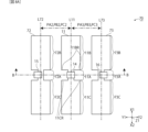
- FIG. 4 is a plan view showing the shape and positional relationship between the bus bar and the magnetic sensor in Embodiment 1.
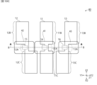
- FIG. 4 is a cross-sectional view showing the shape and positional relationship between the bus bar and the magnetic sensor in Embodiment 1.
- FIG. It is a perspective view which shows the basic composition of a current sensor.
- 1 is an exploded perspective view showing the basic configuration of a current sensor;
- FIG. 11 is a plan view of a busbar and a magnetic sensor in Embodiment 2;
- FIG. 3B is a cross-sectional view taken along line BB of FIG. 3A;
- FIG. 11 is a plan view of a busbar and a magnetic sensor in Embodiment 3;
- 4B is an enlarged plan view of regions C1 and C2 of FIG.
- FIG. 4A; FIG. 4B is an enlarged plan view of region C3 in FIG. 4A;
- FIG. 11 is a plan view of a busbar and a magnetic sensor in Embodiment 4;
- FIG. 5B is a cross-sectional view taken along line BB of FIG. 5A;
- FIG. 12 is a cross-sectional view along line BB according to a modification of Embodiment 4;
- FIG. 20 is a cross-sectional view along the line BB according to another modification of the fourth embodiment;
- FIG. 11 is a plan view of a busbar and a magnetic sensor in Embodiment 5;
- FIG. 14 is a plan view of a busbar and a magnetic sensor in Embodiment 6;
- FIG. 7B is a cross-sectional view taken along line BB of FIG. 7A;
- FIG. 11 is a plan view of a busbar and a magnetic sensor in Embodiment 7;
- FIG. 8B is a cross-sectional view taken along line BB of FIG. 8A; It is a top view which shows the shape of the conventional bus bar and a magnetic sensor, and positional relationship.
- FIG. 9B is a cross-sectional view taken along line BB of FIG. 9A; It is a top view which shows the shape of the conventional bus bar and a magnetic sensor, and positional relationship.
- FIG. 10B is a cross-sectional view taken along line BB of FIG. 10A;
- FIG. 2A is a perspective view showing the current sensor 10
- FIG. 2B is an exploded perspective view of the current sensor 10.
- FIG. The basic configuration of the current sensor 10 will be described using these figures. Note that the size and positional relationship of each member such as the bus bar and the magnetic detection unit will be described using other drawings.
- the current sensor 10 has a substantially rectangular parallelepiped shape by fixing an upper (Z-axis direction Z1 side) cover member 8a and a lower (Z-axis direction Z2 side) case member 8b to each other.
- a housing 8 is provided, and three busbars 11, 12, and 13 penetrate the case member 8b along the width direction (X-axis direction) of the housing 8.
- the busbars 11, 12, and 13 are plate-like conductive members extending in the width direction of the housing 8.
- the normal direction of the plate surfaces is the Z-axis direction, and the two opposing plate surfaces are They are arranged side by side along the Y-axis direction so as to correspond to the top and bottom of the housing 8 .
- Both end portions of the busbars 11, 12, and 13, which are connecting portions to the outside in the X-axis direction, do not necessarily have to be line-symmetrical.
- the circuit board 7 is arranged in the housing 8 along the longitudinal direction.
- Magnetic detectors 14, 15 and 16 are arranged on the circuit board 7 at positions corresponding to the busbars 11, 12 and 13 on the XY plane (the plane including the X axis and the Y axis). At least part of the sensor units in the magnetic detection units 14, 15, and 16 face the corresponding busbars and overlap the facing busbars when viewed along the Z-axis.
- the magnetic detection units 14, 15, and 16 detect the induced magnetic field generated by the currents (measured currents) flowing through the busbars 11, 12, and 13, and measure the current values of the measured currents.
- the magnetic detection units 14, 15, and 16 are desirably provided on the same side surface of the circuit board 7, and are configured using, for example, a magnetoresistive element such as a GMR element (giant magnetoresistive element).
- FIG. 9A is a plan view of busbars 91, 92, 93 and magnetic detectors 94, 95, 96 in a conventional current sensor 90
- FIG. 9B is a cross-sectional view taken along line BB in FIG. 9A.
- the busbars 91, 92, and 93 of the current sensor 90 are arranged along the Y-axis direction with the longitudinal direction thereof being the X-axis direction.
- the bus bar 91 has a wide portion 91B and a wide portion 91C, which are wider in the Y-axis direction than the narrow portion 91A, on both sides of the narrow portion 91A in the X-axis direction.
- the busbars 92, 93 similarly have wide portions 92B, 93B and wide portions 92C, 93C.
- magnetic detectors 94, 95, and 96 are arranged facing narrow portions 91A, 92A, and 93A of busbars 91, 92, and 93, respectively.
- the current sensor 90 detects magnetism based on currents to be measured flowing through the narrow portions 91A, 92A, and 93A by means of magnetic detectors 94, 95, and 96, and measures currents.
- a straight line L94 passing through the center of the Y-axis direction width of the magnetic detection portion 94 and a line L94 passing through the center of the Y-axis direction width of the narrow portion 91A of the busbar 91 It is arranged so as to overlap with the straight line L91A.
- straight lines L95 and L96 passing through the centers of the Y-axis direction widths of the magnetic detection portions 95 and 96, and straight lines L92A and L93A passing through the Y-axis direction width centers of the narrow portions 92A and 93A of the busbars 92 and 93. are shifted in opposite directions in the Y-axis direction. Therefore, the straight line L95 is located on the Y1 side of the straight line L92A, and the straight line L96 is located on the Y2 side of the straight line L93A.
- the magnetic detectors 95 and 96 are arranged so as to approach the busbar 91 side, deviating from the center of the narrow width portions 92A and 93A in the Y-axis direction. Therefore, the influence of the magnetism based on the current to be measured flowing in the corner 91BR on the narrow portion 91A side of the wide portion 91B of the bus bar 91 and the corner 91CR on the narrow portion 91A side of the wide portion 91C is detected by the magnetic detector 95, 96 errors may be caused. In other words, the current flowing through the corners 91BR and 91CR may cause errors in the magnetic detectors 95 and 96 and reduce the measurement accuracy of the current sensor 90 .
- the direction in which the magnetic detection portions 95 and 96 are shifted is important, and the direction in which the magnetic detection portions 95 and 96 are shifted should be the direction away from the narrow portion 91A. , the measurement accuracy of the current sensor 90 is improved. Embodiments of the present invention based on this finding will be described below.
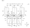
- FIG. 1A is a plan view of busbars 11, 12, 13 and magnetic detectors 14, 15, 16 of current sensor 10, viewing area A1 and area A2 in FIG. 2B along the Z-axis direction.
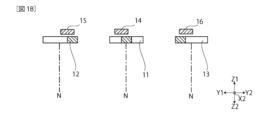
- FIG. 1B is a cross-sectional view taken along line BB of FIG. 1A. The shapes and positional relationships of the busbars 11, 12, 13 and the magnetic detectors 14, 15, 16 will be described with reference to these figures.
- the current sensor 10 includes a plurality of busbars 11, 12 and 13, which are a first busbar, a second busbar, and a third busbar, and a plurality of magnetic sensors, which are a first magnetic detector, a second magnetic detector and a third magnetic detector. It has detectors 14 , 15 and 16 .
- the busbars 11, 12, and 13 extend in the X-axis direction (first direction) and are arranged along the Y-axis direction (second direction) orthogonal to the X-axis direction.
- the magnetic detection units 14 , 15 , 16 can detect magnetic fields generated by currents to be measured flowing through the busbars 11 , 12 , 13 .
- the magnetic detectors 14, 15 and 16 are arranged in this order so as to face the busbars 11, 12 and 13 in the Z-axis direction (third direction) orthogonal to the X-axis direction and the Y-axis direction.
- the busbar 12 is arranged adjacent to the busbar 11 on the Y1 side (one side) of the busbar 11 in the Y-axis direction
- the busbar 13 is arranged on the Y2 side (the other side) of the busbar 11 in the Y-axis direction. is placed adjacent to the
- Each of the busbars 11, 12, and 13 is formed in a plate shape, and as shown in FIG. 1B, is arranged so that the normal line N of the plate surface is in the Z-axis direction.
- the bus bar 11 includes a narrow portion 11A arranged to face the magnetic detection portion 14, a wide portion 11B connected to the X1 side (one side) of the narrow portion 11A in the X-axis direction, and a wide portion 11B connected to the X2 side (the other side) of the narrow portion 11A. and a connected wide portion 11C.
- the wide portion 11B and the wide portion 11C of the busbar 11 are rectangular with the same dimension (width) in the Y-axis direction.
- the wide portion 11B and the wide portion 11C have a larger dimension (width) in the Y-axis direction than the narrow portion 11A.
- the busbars 12 and 13 have narrow width portions 12A and 13A arranged opposite to the magnetic detection portions 15 and 16, and a wide width portion 12B connected to the X1 side of the narrow width portions 12A and 13A in the X-axis direction. , 13B, and wide portions 12C and 13C connected to the X2 side. Moreover, the wide width portions 12B, 13B and the wide width portions 12C, 13C are rectangular with the same dimension in the Y-axis direction. The wide width portions 12B, 13B and the wide width portions 12C, 13C have a larger dimension (width) in the Y-axis direction than the narrow width portions 12A, 13A.
- the Y-axis direction width center 15P of the magnetic detection portion 15 that detects the magnetic field of the busbar 12 is located at the Y-axis direction width center 12AP from the Y-axis direction width center 12AP of the narrow width portion 12A when viewed along the Z-axis direction. are shifted to the Y1 side.
- the center 16P of the width in the Y-axis direction of the magnetic detection portion 16 that detects the magnetic field of the bus bar 13 is arranged to be shifted toward the Y2 side in the Y-axis direction from the center 13AP of the width in the Y-axis direction of the narrow portion 13A. ing. That is, the magnetism detection part 15 and the magnetism detection part 16 are shifted in the direction away from the busbar 11 with respect to the center 12AP and the center 13AP, respectively.
- the magnetic detectors 15 and 16 are shifted away from the bus bar 11 in the Y-axis direction, respectively, so that the magnetic detector 15 is positioned on the Y1 side of the opposed narrow width portion 12A, and the magnetic detector 16 is positioned in the opposed narrow width portion 13A. are arranged on the Y2 side of the . With this arrangement, the distance from the magnetic detector 15 to the busbar 11 and the distance from the magnetic detector 16 to the busbar 11 can be increased. Therefore, the magnetic field generated near the corner 11BR of the wide portion 11B on the narrow portion 11A side and near the corner 11CR of the wide portion 11C on the narrow portion 11A side of the busbar 11 is detected by the magnetic detecting portion 15 and the magnetic detecting portion 16. The measurement accuracy of the current sensor 10 can be improved by suppressing the error due to the influence on the current sensor 10 .
- corner portion 11BR of the wide portion 11B on the side of the narrow portion 11A is, in FIG. 1A, the edge of the wide portion 11B extending in the first direction (X-axis direction) and the boundary between the wide portion 11B and the narrow portion 11A. , and the side extending in the second direction (Y-axis direction) of the wide portion 11B.
- the corner portion 11CR of the wide portion 11C on the side of the narrow portion 11A also has a side extending in the first direction (X-axis direction) of the wide portion 11C and the wide portion 11C formed at the boundary between the wide portion 11C and the narrow portion 11A. and a side extending in the second direction (Y-axis direction).
- the difference in the magnitude of the magnetic flux density also tends to be similar in the bus bar 12, and near the boundary between the wide width portion 12B and the narrow width portion 12A, the magnetic flux density near the straight line L12A increases as the narrow width portion 12A is approached. , the magnetic flux density is relatively small at a distance from the straight line L12A. The same tendency is observed near the boundary between the wide portion 12C and the narrow portion 12A.
- the current densities at the corner portion 11CR of the wide portion 11C of the busbar 11 on the narrow portion 11A side and the corner portion 12CR of the wide portion 12C of the busbar 12 on the narrow portion 12A side are compared.
- the corner portion 12CR on the side of the narrow portion 12A of the wide portion 12C of the busbar 12 is farther from the straight line L12A than the distance between the corner portion 11CR of the busbar 11 and the straight line L11A. Therefore, the current density at the corner portion 12CR on the side of the narrow portion 12A of the wide portion 12C becomes smaller than the current density at the corner portion 11CR of the busbar 11, and becomes a value close to zero. In other words, almost no current flows.
- the magnetic detection portion 14 is brought closer to the corner portion 12CR of the wide portion 12C of the busbar 12.
- a magnetic field large enough to affect the magnetic detection section 14 is not generated from the section 12CR. Therefore, the measurement accuracy of the magnetic detector 14 is not degraded due to the influence of the magnetic field of the corner 12CR.
- the measurement accuracy of the magnetic detector 14 deteriorates due to the influence of the magnetic field generated at the corner 13CR of the wide portion 13C of the busbar 13. never.
- the narrow portions 11A of the busbars 11, the narrow portions 12A of the busbars 12, and the narrow portions 13A of the busbars 13 are arranged at equal intervals in the Y-axis direction. It is That is, the interval PA2 between the narrow portion 11A and the narrow portion 12A in the Y-axis direction is equal to the interval PA3 between the narrow portion 11A and the narrow portion 13A.
- the wide portion 11B of the busbar 11, the wide portion 12B of the busbar 12, and the wide portion 13B of the busbar 13 are arranged at equal intervals in the Y-axis direction, and correspond to the first wide portion.
- a distance PB2 between the wide portion 11B and the wide portion 12B in the Y-axis direction is equal to a distance PB3 between the wide portion 11B and the wide portion 13B.
- the wide portion 11C of the busbar 11, the wide portion 12C of the busbar 12, and the wide portion 13C of the busbar 13 are arranged at equal intervals in the Y-axis direction, and correspond to the second wide portion.
- the interval PC2 between the wide portion 11C and the wide portion 12C in the Y-axis direction is equal to the interval PC3 between the wide portion 11C and the wide portion 13C.
- the magnetic detectors 14, 15, 16 can absorb the influence of magnetic fields other than the busbars 11, 12, 13 facing each other. can be suppressed, and the measurement accuracy of the current sensor 10 is improved.
- the narrow portion 11A of the busbar 11, the narrow portion 12A of the busbar 12, and the narrow portion 13A of the busbar 13 have the same dimension in the Y-axis direction and the same dimension in the X-axis direction. When viewed along the Z-axis direction, they have the same outer shape, and the centers 11AP, 12AP, and 13AP in the Y-axis direction are arranged on the same straight line (BB line). At least part of the narrow portions 11A, 12A, and 13A may be arranged on the straight line BB along the Y-axis direction, and the centers 11AP, 12AP, and 13AP do not need to be arranged.
- the wide portion 11B and the wide portion 12C of the bus bar 11 have the same dimension in the Y-axis direction.
- the wide portion 12B of the busbar 12 and the wide portion 12C of the busbar 12 have the same dimension in the Y-axis direction.
- the wide portion 13B and the wide portion 13C of the bus bar 13 have the same dimension in the second direction.
- busbars 11, 12, 13 By forming the busbars 11, 12, 13 into the above-described shape and arrangement, the influence of the busbars other than the detection target busbars 11, 12, 13 facing the magnetic detection units 14, 15, 16 is suppressed, and the magnetic detection units 14, 15, 16 Errors in measurement accuracy due to 14, 15 and 16 can be suppressed. Further, by arranging the narrow width portions 11A, 12A, 13A as described above, the size of the magnetic detection portions 14, 15, 16 facing them in the X-axis direction can be reduced.
- the busbar 11 When viewed along the Z-axis direction, the busbar 11 has a shape symmetrical with respect to a straight line L11A passing through the center 11AP of the narrow portion 12A of the busbar 11 and parallel to the X-axis direction.
- the busbar 12 and the busbar 13 are symmetrical with respect to a straight line L12A-13A passing through the center of the straight line L12A and the straight line L13A in the Y-axis direction and parallel to the X-axis direction.
- the center of the straight line L12A and the straight line L13A in the Y-axis direction overlaps the center 11AP of the narrow portion 11A.
- a straight line L11A which is the first center line of the narrow portion 11A of the busbar 11, and a second centerline between the narrow portion 12A of the busbar 12 and the narrow portion 13A of the busbar 13. and the straight line L12A-13B are overlapped. Since the shape of busbar 11 is axisymmetric, straight lines L11B and 11C also overlap both straight line L11A as the first center line and straight line L12A-13B as the second center line. With this configuration, it is possible to suppress the influence on the magnetic detection units 14, 15, and 16 of the busbars 11, 12, and 13 other than those to be detected.
- a straight line L14 passing through the center 14P of the magnetic detection unit 14 for detecting the magnetic field of the busbar 11 in the Y-axis direction is aligned with the busbar 11 when viewed along the Z-axis direction. is shifted in the Y1 direction with respect to the narrow portion 11A so as to be positioned in the Y1 direction with respect to a straight line L11AP passing through the center 11AP in the Y-axis direction of the narrow portion 11A.
- the current sensor is installed, for example, in the inverter of an automobile.
- a current sensor would be attached between the power module and the motor to measure the current flowing therebetween.
- a power module and a motor often have different terminal pitches.
- the terminal pitch of the current sensor By setting the terminal pitch of the current sensor to be different between the input side and the output side, there is no need for a member for pitch adjustment, which is effective in terms of ease of installation and environmental load resistance.
- the current sensor 10 including the busbars 11, 12, and 13 with different pitches on the X1 side and the X2 side, like the conventional current sensor 90 shown in FIG.
- the magnetic detection portions 15 and 16 facing the narrow portion 13A are shifted toward the busbar 11, the distances between the magnetic detection portions 15 and 16 and the corner portions 11BR and 11CR of the busbar 11 become shorter. Therefore, errors in the magnetic detectors 15 and 16 due to the influence of the bus bar 11 increase.
- the magnetic detectors 15 and 16 are made less susceptible to the influence of the corners 11BR and 11CR of the busbar 11. Therefore, the magnetic detectors 15 and 16 are arranged in the direction away from the narrow portion 11A of the busbar 11 in the Y-axis direction. That is, the magnetic detector 15 is shifted to the Y1 side, and the magnetic detector 16 is shifted to the Y2 side.
- the magnetic sensors facing the busbars on both sides are arranged so that the distance from the central busbar in the Y-axis direction increases.
- FIG. 3A is a plan view showing the busbars 21, 12, 13 and the magnetic detection units 14, 15, 16 of the current sensor 20 according to this embodiment
- FIG. 3B is a cross-sectional view taken along line BB in FIG. 3A.
- the busbar 21 is not line-symmetrical like the busbar 11 of the first embodiment, but has a shape in which the narrow portion 21A is shifted in the Y2 direction when viewed along the Z-axis direction. Different from the sensor 10 .
- the magnetic detectors 14, 15, and 16 can be arranged at regular intervals in the Y-axis direction.
- the distance PD5 in the Y-axis direction between the magnetic detection units 14 and 15 and the distance PD6 in the Y-axis direction between the magnetic detection units 14 and 16 are equal to each other.
- 15 and 16 are arranged so that the intervals (pitch) are equal.
- the current sensor 20 shifts the narrow portion 21A of the busbar 21 located in the middle in the Y2 direction with respect to straight lines L21B and L21C passing through the center of the wide portion 21B and wide portion 21C in the Y-axis direction and parallel to the X-axis.
- This configuration differs from the embodiment of the current sensor 10 shown in FIG. 1A. Therefore, the space PA2 between the narrow width portions 21A and 12A is larger than the space PA3 between the narrow width portions 21A and 13A.
- FIG. 4A is a plan view showing the busbar and the magnetic detection portion of the current sensor 30 according to the present embodiment
- FIG. 4B is an enlarged plan view of regions C1 and C2 in FIG. 4A
- FIG. 4C is a region C3 in FIG. 4A. It is an enlarged plan view.
- the magnetic detectors 14, 15 and 16 of the current sensor 30 have the same specifications. However, when viewed along the Z-axis direction, the arrangement direction of the magnetic detection section 16 is opposite to the arrangement direction of the magnetic detection section 15 in the X-axis direction and the Y-axis direction.
- the magnetic detection unit 15 is arranged in the same direction as the magnetic detection unit 14 in the X-axis direction and the Y-axis direction. are placed in the opposite direction. That is, the magnetic detection section 16 is equivalent to a configuration in which the magnetic detection section 14 is rotated 180° on the XY plane about the center 16P.
- the magnetic detection portion 14 when viewed along the Z-axis direction, the magnetic detection portion 14 is arranged to be shifted in the Y-axis direction Y1 with respect to the narrow portion 11A of the busbar 11.
- the magnetic detector 15 is also arranged to be shifted in the Y-axis direction Y1 with respect to the narrow portion 12A of the busbar 12 . Since the magnetic detectors 14 and 15 are arranged to be shifted in the same direction with respect to the corresponding narrow width portions, the magnetic detectors 14 and 15 are arranged in the same direction.
- the orientation of the magnetic detector 14 is the same as that of the magnetic detector 16.
- the magnetic detection units 14, 15, and 16 have sensor units 142, 152, and 162 for detecting magnetism and signal terminals for output to the outside on main bodies 141, 151, and 161.
- the signal terminals 143 and 153 and the power terminals 144 and 154 are provided so as to protrude from the sensor portions 142 and 152 in the Y1 direction.
- the signal terminal 163 and the power terminal 164 are provided so as to protrude from the sensor section 162 in the Y2 direction.
- the signal terminals 143, 153, 163 and the power terminals 144, 154, 164 are arranged at positions not overlapping the narrow portions 11A, 12A, 13A of the busbars 11, 12, 13 when viewed along the Z-axis direction. ing. Although FIGS. 4B and 4C show only the signal terminals 143, 153, 163 and the power terminals 144, 154, 164, general terminals for other purposes may be provided.
- the magnetic detection section 15 and the magnetic detection section 16 are arranged to be shifted to the opposite side in the Y-axis with respect to the narrow width portions 12A and 13A. Therefore, if the magnetic detection section 16 is arranged in the same direction as the magnetic detection section 15 shown in FIG. 4B, the signal terminal 163 and the power terminal 164 overlap the narrow portion 13A when viewed along the Z-axis direction. Therefore, as shown in FIG. 4C, the magnetic detection section 16 is arranged in the opposite direction to the magnetic detection section 15 in FIG. 4A.
- one side surface of the main body 141, 151, 161 provided with the signal terminals 143, 153, 163 and the power terminals 144, 154, 164 can be arranged away from the narrow portions 11A, 12A, 13A. can.
- the magnetic detection units 14 and 15 and the magnetic detection unit 16 are arranged to be shifted to the opposite side of the Y-axis with respect to the narrow width portions 11A, 12A, and 13A, the magnetism detected by the magnetic detection unit 16 is , the direction opposite to that of the magnetic detectors 14 and 15 . Therefore, the current sensor 30 is controlled so that the output from the magnetic detector 16 is electrically inverted.
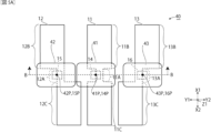
- FIG. 5A is a plan view showing busbars 11, 12, 13 and magnetic detectors 14, 15, 16 of current sensor 40 according to the present embodiment
- FIG. 5B is a cross-sectional view taken along line BB in FIG. 5A
- the current sensor 40 of this embodiment differs from the current sensor 10 in that it has shields 41 , 42 and 43 .
- the shields 41 , 42 , 43 are made of flat metal plates, and are arranged on at least one of the Z1 side and the Z2 side of the magnetic detectors 14 , 15 , 16 in the Z-axis direction. When viewed along the Z-axis direction, the centers 41P, 42P, 43P of the shields 41, 42, 43 and the magnetic detectors 14, 15, 16 are arranged at overlapping positions.
- the shields 41 are arranged on both sides of the Z1 side and the Z2 side so as to face each other in parallel. Also, the shield 41 is arranged at a position where the center 41P and the center 14P of the magnetic detection section 14 overlap when viewed along the Z-axis.
- Each of the shields 41, 42, and 43 is preferably formed of a ferromagnetic material as a magnetic shield made of a magnetic material, and has a configuration in which a plurality of metal plates having the same rectangular shape and the same size in a plan view are stacked vertically. ing.
- the shield 41 has a size that covers the narrow portion 11A and the magnetic detection portion 14 in the width direction (X-axis direction) and the longitudinal direction (Y-axis direction).
- the two shields 41 overlap each other so as not to protrude when viewed along the Z-axis direction.
- the magnetic detection unit 14 blocks an external magnetic field (external magnetic field) such as an induced magnetic field caused by the current flowing through the adjacent busbars 12 and 13. You can reduce its impact.
- the shield 42 that covers the narrow portion 12A and the magnetic detection portion 15, and the shield 42 that covers the narrow portion 13A and the magnetic detection portion 16 are configured similarly to the shield 41.
- a configuration in which only one each of the shields 41, 42, and 43 is provided may be employed.
- FIG. 5C is a cross-sectional view of the shields 44, 45, and 46 according to the modification at a portion corresponding to line BB in FIG. 5A.
- the shield 44 has a facing portion 44A arranged in the Z-axis direction, and side portions 44B and 44B projecting from both ends 44AE and 44AE of 44A toward the Z1 side in the Z-axis direction.
- the facing portion 44A is arranged on the Z2 side of the magnetic detection portion 14 and the busbar 11 in the Z-axis direction.
- the side portions 44B, 44B are arranged on both sides of the magnetic detection portion 14 and the bus bar 11 in the Y-axis direction, respectively.
- the opposing portion 44A is arranged on the Z2 side in the example shown in FIG. 5C, it may be on the Z1 side.
- the shields 45 and 46 like the shield 44, have facing portions 45A and 46A, one ends 45AE and 46AE, and side portions 45B and 46B.
- the facing portions 45A and 46A are arranged on one side of the magnetic detection portions 15 and 16 and the busbars 12 and 13 in the Z-axis direction.
- the side portions 45B and 46B are arranged at one ends 45AE and 46AE on both sides of the opposing portions 45A and 46A in the Y-axis direction.
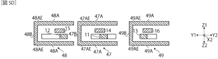
- FIG. 5D is a cross-sectional view of shields 47, 48, and 49 according to a modification at a portion corresponding to line BB in FIG. 5A.
- the shield 47 includes facing portions 47A, 47A arranged so that the plate surfaces face each other with a space in the Z-axis direction; have.
- the facing portion 47A is arranged on both sides of the magnetic detection portion 14 and the bus bar 11 in the Z-axis direction, that is, on the Z1 side and the Z2 side.
- the connecting portion 47B is arranged on one side of the magnetic detecting portion 14 and the bus bar 11 in the Y-axis direction. Although the connecting portion 47B is arranged on the Y1 side in the example shown in FIG. 5D, it may be on the Y2 side.
- the shields 48 and 49 have opposing portions 48A and 49A, one ends 48AE and 49AE, and connecting portions 48B and 49B. placed on one side.
- the circuit board 7 (see FIGS. 2A and 2B) on which the magnetic detectors 14, 15, and 16 are mounted is provided with slits (not shown) into which the connecting portions 47B, 48B, and 49B can be inserted along the X axis.
- the circuit board 7 is inserted from the X2 direction and arranged in the case member 8b.
- a notch portion (not shown) having a size into which the circuit board 7 can be inserted may be provided at the upper end (Z1 side end portion) of the X2 side wall portion of the case member 8b.
- a protrusion (not shown) that engages with the notch is provided at the lower end (Z2 side end) of the X2 side wall of the cover member 8a, the circuit board 7 can be easily inserted.
- foreign matter can be prevented from entering the inside of the current sensor 40 by covering the notch with the protrusion.
- the current sensor 40 may be configured differently from that shown in FIG. 2 as follows.
- the directions, names and symbols in FIGS. 2 and 5D are used in the following description.
- the case member 8b has an internal space that opens in the X2 direction, and one and the other opposing portions of a plurality of shields are embedded in the wall portions on the Z1 direction side and the Z2 direction side, respectively.
- the circuit board 7 has slits into which the connecting portions 47B, 48B, and 49B can be inserted and is open on the X1 direction side, and is configured to be insertable into the case member 8b from the X2 direction side.
- the cover member 8a is locked on the X2 direction side of the cover member 8a so as to cover the opening of the case member 8b. With such a configuration, the positioning accuracy of each shield is improved.
- FIG. 6 is a plan view showing the busbars 11, 52, 53 and the magnetic detectors 14, 15, 16 of the current sensor 50 according to this embodiment.
- a current sensor 50 shown in the figure differs from the current sensor 10 in that busbars 52 and 53 are provided with narrow portions 52A and 53A formed in a stepped shape.
- the narrow portions 11A, 11A, 11A when viewed along the Z-axis, like the current sensors 10, 20, 30, and 40, the narrow portions 11A, 11A, 11A It is preferable that the ends (end surfaces) of 12A and 13A in the Y-axis direction form straight lines parallel to the X-axis. This shape makes it easier for the detection magnetic field based on the current to be detected to be formed parallel to the detection direction of the magnetic detection units 14 , 15 , and 16 .
- the Y2 side end surface (the other side end surface) of the narrow portion 13A in the Y axis direction and the Y2 side end surface (the other side end surface) of the wide portion 13C in the Y axis direction are flush with each other.
- the current in the narrow portions 12A and 13A flows along the X-axis direction, so that the magnetism generated by the current can be accurately detected by the magnetic detectors 15 and 16 . Therefore, it is possible to reduce the measurement error caused by the components of the detected magnetic field oblique to the detection direction.
- FIG. 7A is a plan view showing the busbars 11, 12, 13 and the magnetic detection units 14, 15, 16 of the current sensor 60 according to this embodiment
- FIG. 7B is a cross-sectional view taken along line BB in FIG. 7A.
- the current sensor 60 differs from the current sensor 10 in that the magnetic detection portion 14 is arranged without being shifted from the facing narrow portion 11A when viewed along the Z-axis direction. That is, in the current sensor 60, when viewed along the Z-axis direction, the X-axis direction straight line L14 passing through the Y-axis direction center 14P of the magnetic detection portion 14 is aligned with the Y-axis direction center 11AP of the narrow portion 11A.
- FIG. 8A is a plan view of the busbars 11, 72, 73 and the magnetic detectors 14, 15, 16 in the current sensor 70 according to this embodiment
- FIG. 8B is a cross-sectional view taken along line BB in FIG. 8A.
- bus bars 11, 72, and 73 have the same shape, and straight lines L11, 72, and 73 in the X-axis direction passing through the midpoints of the bus bars in the Y-axis direction are equally spaced in the Y-axis direction. are arranged so that
- the current sensor 70 having the busbars 11, 72, and 73 of the same shape, due to the arrangement of the magnetic detection unit 15 and the magnetic detection unit 16, the current sensor having the busbars with different pitches on the X1 side and the X2 side may differ. It has the same effect. That is, in the current sensor 70, when viewed along the Z-axis, the magnetic detection unit 15 and the magnetic detection unit 16 are arranged in opposite directions in the Y-axis direction (Y1 side and Y2 side) with respect to 72A and 73A. They are staggered. With this arrangement, the influence of the magnetic field generated near the corners 11BR and 11CR of the busbar 11 on the magnetic detectors 15 and 16 can be suppressed, and the measurement accuracy of the current sensor 70 can be improved.
- FIG. 10A is a plan view showing busbars 11, 12, 13 and magnetic detectors 14, 15, 16 of a current sensor 80 of a comparative example
- FIG. 10B is a cross-sectional view taken along line BB in FIG. 10A.
- the current sensor 80 differs from the current sensor 40 only in that the magnetic detection portion 16 is shifted in the Y1 direction instead of the Y2 direction with respect to the narrow portion 13A when viewed along the Z-axis, and other configurations are the same. is.
- the present invention is useful as a current sensor with excellent measurement accuracy that has three channels for measuring mutually related currents such as three-phase alternating current.
- circuit board 8 housing 8a: cover member 8b: case member 10: current sensor 11: bus bar (first bus bar) 12: Busbar (second busbar) 13: Busbar (third busbar) 11A, 12A, 13A: Narrow portions 11AP, 12AP, 13AP: Centers 11B, 12B, 13B: Wide portions (first wide portions) 11BR: corner portions 11C, 12C, 13C: wide portion (second wide portion) 11CR, 12CR, 13CR: corner portion 14: magnetic detection portion (first magnetic detection portion) 15: magnetic detection unit (second magnetic detection unit) 16: magnetic detection unit (third magnetic detection unit) 14P, 15P, 16P: center 20: current sensor 21: bus bar (first bus bar) 21A: narrow portion 21B: wide portion (first wide portion) 21C: wide part (second wide part) 30: Current sensors 141, 151, 161: Main bodies 142, 152, 162: Sensor units 143, 153, 163: Signal terminals 144, 154, 164: Power terminals 40: Current sensors 41: Current
Landscapes
- Physics & Mathematics (AREA)
- General Physics & Mathematics (AREA)
- Measuring Instrument Details And Bridges, And Automatic Balancing Devices (AREA)
- Condensed Matter Physics & Semiconductors (AREA)
Priority Applications (5)
| Application Number | Priority Date | Filing Date | Title |
|---|---|---|---|
| JP2023556137A JP7615344B2 (ja) | 2021-10-29 | 2022-08-09 | 電流センサ |
| EP22884769.5A EP4425193A4 (en) | 2021-10-29 | 2022-08-09 | CURRENT SENSOR |
| CN202280072778.6A CN118176426A (zh) | 2021-10-29 | 2022-08-09 | 电流传感器 |
| KR1020247008827A KR20240050379A (ko) | 2021-10-29 | 2022-08-09 | 전류 센서 |
| US18/620,579 US12571820B2 (en) | 2021-10-29 | 2024-03-28 | Current sensor |
Applications Claiming Priority (2)
| Application Number | Priority Date | Filing Date | Title |
|---|---|---|---|
| JP2021-177946 | 2021-10-29 | ||
| JP2021177946 | 2021-10-29 |
Related Child Applications (1)
| Application Number | Title | Priority Date | Filing Date |
|---|---|---|---|
| US18/620,579 Continuation US12571820B2 (en) | 2021-10-29 | 2024-03-28 | Current sensor |
Publications (1)
| Publication Number | Publication Date |
|---|---|
| WO2023074083A1 true WO2023074083A1 (ja) | 2023-05-04 |
Family
ID=86159322
Family Applications (1)
| Application Number | Title | Priority Date | Filing Date |
|---|---|---|---|
| PCT/JP2022/030372 Ceased WO2023074083A1 (ja) | 2021-10-29 | 2022-08-09 | 電流センサ |
Country Status (6)
| Country | Link |
|---|---|
| US (1) | US12571820B2 (https=) |
| EP (1) | EP4425193A4 (https=) |
| JP (1) | JP7615344B2 (https=) |
| KR (1) | KR20240050379A (https=) |
| CN (1) | CN118176426A (https=) |
| WO (1) | WO2023074083A1 (https=) |
Citations (8)
| Publication number | Priority date | Publication date | Assignee | Title |
|---|---|---|---|---|
| WO2013005458A1 (ja) * | 2011-07-04 | 2013-01-10 | アルプス・グリーンデバイス株式会社 | 電流センサ |
| JP2015190781A (ja) * | 2014-03-27 | 2015-11-02 | ヤマハ株式会社 | 基板 |
| JP2018096795A (ja) * | 2016-12-12 | 2018-06-21 | 株式会社デンソー | 電流センサ |
| US20180238938A1 (en) * | 2017-02-17 | 2018-08-23 | Allegro Microsystems, Llc | Current Sensor System |
| JP2019138815A (ja) * | 2018-02-13 | 2019-08-22 | 日立金属株式会社 | 電流センサ |
| CN110221112A (zh) * | 2019-06-04 | 2019-09-10 | 苏州汇川技术有限公司 | 电路板及电力电子设备 |
| JP2020148484A (ja) * | 2019-03-11 | 2020-09-17 | トヨタ自動車株式会社 | 電流検出装置 |
| JP2021039030A (ja) | 2019-09-04 | 2021-03-11 | 株式会社デンソー | 電流センサ |
Family Cites Families (10)
| Publication number | Priority date | Publication date | Assignee | Title |
|---|---|---|---|---|
| US7898240B2 (en) * | 2005-02-23 | 2011-03-01 | Asahi Kasei Emd Corporation | Current measuring apparatus |
| JP5153491B2 (ja) * | 2008-07-11 | 2013-02-27 | 矢崎総業株式会社 | 電流検出装置 |
| JP6018544B2 (ja) * | 2013-05-20 | 2016-11-02 | 本田技研工業株式会社 | 電流センサユニット |
| JP2015194472A (ja) | 2014-01-23 | 2015-11-05 | 株式会社デンソー | 電流検出システム |
| JP6973021B2 (ja) * | 2017-12-18 | 2021-11-24 | 日立金属株式会社 | 電流センサ |
| EP3508863B1 (en) | 2018-01-05 | 2023-06-07 | Melexis Technologies SA | Offset current sensor structure |
| JP7295262B2 (ja) * | 2019-10-08 | 2023-06-20 | アルプスアルパイン株式会社 | 電流検出装置 |
| JP7466646B2 (ja) * | 2020-07-14 | 2024-04-12 | アルプスアルパイン株式会社 | 電流検出装置 |
| JP7452398B2 (ja) * | 2020-12-02 | 2024-03-19 | 株式会社デンソー | 電流センサ |
| JP2025097725A (ja) * | 2023-12-19 | 2025-07-01 | アルプスアルパイン株式会社 | 電流センサおよびバスバ |
-
2022
- 2022-08-09 EP EP22884769.5A patent/EP4425193A4/en active Pending
- 2022-08-09 KR KR1020247008827A patent/KR20240050379A/ko not_active Ceased
- 2022-08-09 CN CN202280072778.6A patent/CN118176426A/zh active Pending
- 2022-08-09 JP JP2023556137A patent/JP7615344B2/ja active Active
- 2022-08-09 WO PCT/JP2022/030372 patent/WO2023074083A1/ja not_active Ceased
-
2024
- 2024-03-28 US US18/620,579 patent/US12571820B2/en active Active
Patent Citations (8)
| Publication number | Priority date | Publication date | Assignee | Title |
|---|---|---|---|---|
| WO2013005458A1 (ja) * | 2011-07-04 | 2013-01-10 | アルプス・グリーンデバイス株式会社 | 電流センサ |
| JP2015190781A (ja) * | 2014-03-27 | 2015-11-02 | ヤマハ株式会社 | 基板 |
| JP2018096795A (ja) * | 2016-12-12 | 2018-06-21 | 株式会社デンソー | 電流センサ |
| US20180238938A1 (en) * | 2017-02-17 | 2018-08-23 | Allegro Microsystems, Llc | Current Sensor System |
| JP2019138815A (ja) * | 2018-02-13 | 2019-08-22 | 日立金属株式会社 | 電流センサ |
| JP2020148484A (ja) * | 2019-03-11 | 2020-09-17 | トヨタ自動車株式会社 | 電流検出装置 |
| CN110221112A (zh) * | 2019-06-04 | 2019-09-10 | 苏州汇川技术有限公司 | 电路板及电力电子设备 |
| JP2021039030A (ja) | 2019-09-04 | 2021-03-11 | 株式会社デンソー | 電流センサ |
Non-Patent Citations (1)
| Title |
|---|
| See also references of EP4425193A4 |
Also Published As
| Publication number | Publication date |
|---|---|
| KR20240050379A (ko) | 2024-04-18 |
| EP4425193A4 (en) | 2026-01-21 |
| CN118176426A (zh) | 2024-06-11 |
| JPWO2023074083A1 (https=) | 2023-05-04 |
| US20240241156A1 (en) | 2024-07-18 |
| EP4425193A1 (en) | 2024-09-04 |
| US12571820B2 (en) | 2026-03-10 |
| JP7615344B2 (ja) | 2025-01-16 |
Similar Documents
| Publication | Publication Date | Title |
|---|---|---|
| JP6149885B2 (ja) | 電流センサ | |
| JP6030866B2 (ja) | 電流センサ | |
| US10877075B2 (en) | Current sensor | |
| JP7295262B2 (ja) | 電流検出装置 | |
| WO2015033541A1 (ja) | 電流センサ | |
| JP2016200436A (ja) | 電流センサ | |
| JP2008039734A (ja) | 電流センサ | |
| US20250147075A1 (en) | Current Sensor | |
| CN115698730A (zh) | 电流检测装置 | |
| JP7615344B2 (ja) | 電流センサ | |
| JP7242887B2 (ja) | 電流検出装置 | |
| JP7765199B2 (ja) | 電流検出装置及び該装置の回路部 | |
| JP4873348B2 (ja) | 電流センサおよび電流検出装置 | |
| JP5952650B2 (ja) | 電流センサ | |
| CN113884738A (zh) | 用于测量电流的传感器装置和方法 | |
| WO2025027904A1 (ja) | 電流センサ | |
| WO2025263082A1 (ja) | 電流センサ | |
| US20250224429A1 (en) | Current Sensor | |
| WO2024085258A1 (ja) | 電流センサ |
Legal Events
| Date | Code | Title | Description |
|---|---|---|---|
| 121 | Ep: the epo has been informed by wipo that ep was designated in this application |
Ref document number: 22884769 Country of ref document: EP Kind code of ref document: A1 |
|
| WWE | Wipo information: entry into national phase |
Ref document number: 2023556137 Country of ref document: JP |
|
| ENP | Entry into the national phase |
Ref document number: 20247008827 Country of ref document: KR Kind code of ref document: A |
|
| WWE | Wipo information: entry into national phase |
Ref document number: 202280072778.6 Country of ref document: CN |
|
| WWE | Wipo information: entry into national phase |
Ref document number: 2022884769 Country of ref document: EP |
|
| NENP | Non-entry into the national phase |
Ref country code: DE |
|
| ENP | Entry into the national phase |
Ref document number: 2022884769 Country of ref document: EP Effective date: 20240529 |