WO2023067908A1 - 有機el表示装置 - Google Patents
有機el表示装置 Download PDFInfo
- Publication number
- WO2023067908A1 WO2023067908A1 PCT/JP2022/032960 JP2022032960W WO2023067908A1 WO 2023067908 A1 WO2023067908 A1 WO 2023067908A1 JP 2022032960 W JP2022032960 W JP 2022032960W WO 2023067908 A1 WO2023067908 A1 WO 2023067908A1
- Authority
- WO
- WIPO (PCT)
- Prior art keywords
- layer
- organic
- display device
- photosensitive composition
- light
- Prior art date
- Legal status (The legal status is an assumption and is not a legal conclusion. Google has not performed a legal analysis and makes no representation as to the accuracy of the status listed.)
- Ceased
Links
Images



Classifications
-
- H—ELECTRICITY
- H10—SEMICONDUCTOR DEVICES; ELECTRIC SOLID-STATE DEVICES NOT OTHERWISE PROVIDED FOR
- H10K—ORGANIC ELECTRIC SOLID-STATE DEVICES
- H10K59/00—Integrated devices, or assemblies of multiple devices, comprising at least one organic light-emitting element covered by group H10K50/00
- H10K59/10—OLED displays
- H10K59/12—Active-matrix OLED [AMOLED] displays
- H10K59/122—Pixel-defining structures or layers, e.g. banks
-
- G—PHYSICS
- G03—PHOTOGRAPHY; CINEMATOGRAPHY; ANALOGOUS TECHNIQUES USING WAVES OTHER THAN OPTICAL WAVES; ELECTROGRAPHY; HOLOGRAPHY
- G03F—PHOTOMECHANICAL PRODUCTION OF TEXTURED OR PATTERNED SURFACES, e.g. FOR PRINTING, FOR PROCESSING OF SEMICONDUCTOR DEVICES; MATERIALS THEREFOR; ORIGINALS THEREFOR; APPARATUS SPECIALLY ADAPTED THEREFOR
- G03F7/00—Photomechanical, e.g. photolithographic, production of textured or patterned surfaces, e.g. printing surfaces; Materials therefor, e.g. comprising photoresists; Apparatus specially adapted therefor
- G03F7/004—Photosensitive materials
-
- G—PHYSICS
- G03—PHOTOGRAPHY; CINEMATOGRAPHY; ANALOGOUS TECHNIQUES USING WAVES OTHER THAN OPTICAL WAVES; ELECTROGRAPHY; HOLOGRAPHY
- G03F—PHOTOMECHANICAL PRODUCTION OF TEXTURED OR PATTERNED SURFACES, e.g. FOR PRINTING, FOR PROCESSING OF SEMICONDUCTOR DEVICES; MATERIALS THEREFOR; ORIGINALS THEREFOR; APPARATUS SPECIALLY ADAPTED THEREFOR
- G03F7/00—Photomechanical, e.g. photolithographic, production of textured or patterned surfaces, e.g. printing surfaces; Materials therefor, e.g. comprising photoresists; Apparatus specially adapted therefor
- G03F7/004—Photosensitive materials
- G03F7/027—Non-macromolecular photopolymerisable compounds having carbon-to-carbon double bonds, e.g. ethylenic compounds
-
- G—PHYSICS
- G03—PHOTOGRAPHY; CINEMATOGRAPHY; ANALOGOUS TECHNIQUES USING WAVES OTHER THAN OPTICAL WAVES; ELECTROGRAPHY; HOLOGRAPHY
- G03F—PHOTOMECHANICAL PRODUCTION OF TEXTURED OR PATTERNED SURFACES, e.g. FOR PRINTING, FOR PROCESSING OF SEMICONDUCTOR DEVICES; MATERIALS THEREFOR; ORIGINALS THEREFOR; APPARATUS SPECIALLY ADAPTED THEREFOR
- G03F7/00—Photomechanical, e.g. photolithographic, production of textured or patterned surfaces, e.g. printing surfaces; Materials therefor, e.g. comprising photoresists; Apparatus specially adapted therefor
- G03F7/004—Photosensitive materials
- G03F7/027—Non-macromolecular photopolymerisable compounds having carbon-to-carbon double bonds, e.g. ethylenic compounds
- G03F7/032—Non-macromolecular photopolymerisable compounds having carbon-to-carbon double bonds, e.g. ethylenic compounds with binders
- G03F7/033—Non-macromolecular photopolymerisable compounds having carbon-to-carbon double bonds, e.g. ethylenic compounds with binders the binders being polymers obtained by reactions only involving carbon-to-carbon unsaturated bonds, e.g. vinyl polymers
-
- G—PHYSICS
- G03—PHOTOGRAPHY; CINEMATOGRAPHY; ANALOGOUS TECHNIQUES USING WAVES OTHER THAN OPTICAL WAVES; ELECTROGRAPHY; HOLOGRAPHY
- G03F—PHOTOMECHANICAL PRODUCTION OF TEXTURED OR PATTERNED SURFACES, e.g. FOR PRINTING, FOR PROCESSING OF SEMICONDUCTOR DEVICES; MATERIALS THEREFOR; ORIGINALS THEREFOR; APPARATUS SPECIALLY ADAPTED THEREFOR
- G03F7/00—Photomechanical, e.g. photolithographic, production of textured or patterned surfaces, e.g. printing surfaces; Materials therefor, e.g. comprising photoresists; Apparatus specially adapted therefor
- G03F7/004—Photosensitive materials
- G03F7/038—Macromolecular compounds which are rendered insoluble or differentially wettable
-
- G—PHYSICS
- G03—PHOTOGRAPHY; CINEMATOGRAPHY; ANALOGOUS TECHNIQUES USING WAVES OTHER THAN OPTICAL WAVES; ELECTROGRAPHY; HOLOGRAPHY
- G03F—PHOTOMECHANICAL PRODUCTION OF TEXTURED OR PATTERNED SURFACES, e.g. FOR PRINTING, FOR PROCESSING OF SEMICONDUCTOR DEVICES; MATERIALS THEREFOR; ORIGINALS THEREFOR; APPARATUS SPECIALLY ADAPTED THEREFOR
- G03F7/00—Photomechanical, e.g. photolithographic, production of textured or patterned surfaces, e.g. printing surfaces; Materials therefor, e.g. comprising photoresists; Apparatus specially adapted therefor
- G03F7/004—Photosensitive materials
- G03F7/039—Macromolecular compounds which are photodegradable, e.g. positive electron resists
-
- G—PHYSICS
- G03—PHOTOGRAPHY; CINEMATOGRAPHY; ANALOGOUS TECHNIQUES USING WAVES OTHER THAN OPTICAL WAVES; ELECTROGRAPHY; HOLOGRAPHY
- G03F—PHOTOMECHANICAL PRODUCTION OF TEXTURED OR PATTERNED SURFACES, e.g. FOR PRINTING, FOR PROCESSING OF SEMICONDUCTOR DEVICES; MATERIALS THEREFOR; ORIGINALS THEREFOR; APPARATUS SPECIALLY ADAPTED THEREFOR
- G03F7/00—Photomechanical, e.g. photolithographic, production of textured or patterned surfaces, e.g. printing surfaces; Materials therefor, e.g. comprising photoresists; Apparatus specially adapted therefor
- G03F7/004—Photosensitive materials
- G03F7/09—Photosensitive materials characterised by structural details, e.g. supports, auxiliary layers
- G03F7/095—Photosensitive materials characterised by structural details, e.g. supports, auxiliary layers having more than one photosensitive layer
-
- G—PHYSICS
- G03—PHOTOGRAPHY; CINEMATOGRAPHY; ANALOGOUS TECHNIQUES USING WAVES OTHER THAN OPTICAL WAVES; ELECTROGRAPHY; HOLOGRAPHY
- G03F—PHOTOMECHANICAL PRODUCTION OF TEXTURED OR PATTERNED SURFACES, e.g. FOR PRINTING, FOR PROCESSING OF SEMICONDUCTOR DEVICES; MATERIALS THEREFOR; ORIGINALS THEREFOR; APPARATUS SPECIALLY ADAPTED THEREFOR
- G03F7/00—Photomechanical, e.g. photolithographic, production of textured or patterned surfaces, e.g. printing surfaces; Materials therefor, e.g. comprising photoresists; Apparatus specially adapted therefor
- G03F7/004—Photosensitive materials
- G03F7/09—Photosensitive materials characterised by structural details, e.g. supports, auxiliary layers
- G03F7/105—Photosensitive materials characterised by structural details, e.g. supports, auxiliary layers having substances, e.g. indicators, for forming visible images
-
- G—PHYSICS
- G03—PHOTOGRAPHY; CINEMATOGRAPHY; ANALOGOUS TECHNIQUES USING WAVES OTHER THAN OPTICAL WAVES; ELECTROGRAPHY; HOLOGRAPHY
- G03F—PHOTOMECHANICAL PRODUCTION OF TEXTURED OR PATTERNED SURFACES, e.g. FOR PRINTING, FOR PROCESSING OF SEMICONDUCTOR DEVICES; MATERIALS THEREFOR; ORIGINALS THEREFOR; APPARATUS SPECIALLY ADAPTED THEREFOR
- G03F7/00—Photomechanical, e.g. photolithographic, production of textured or patterned surfaces, e.g. printing surfaces; Materials therefor, e.g. comprising photoresists; Apparatus specially adapted therefor
- G03F7/20—Exposure; Apparatus therefor
- G03F7/22—Exposing sequentially with the same light pattern different positions of the same surface
-
- H—ELECTRICITY
- H05—ELECTRIC TECHNIQUES NOT OTHERWISE PROVIDED FOR
- H05B—ELECTRIC HEATING; ELECTRIC LIGHT SOURCES NOT OTHERWISE PROVIDED FOR; CIRCUIT ARRANGEMENTS FOR ELECTRIC LIGHT SOURCES, IN GENERAL
- H05B33/00—Electroluminescent light sources
- H05B33/12—Light sources with substantially two-dimensional [2D] radiating surfaces
-
- H—ELECTRICITY
- H05—ELECTRIC TECHNIQUES NOT OTHERWISE PROVIDED FOR
- H05B—ELECTRIC HEATING; ELECTRIC LIGHT SOURCES NOT OTHERWISE PROVIDED FOR; CIRCUIT ARRANGEMENTS FOR ELECTRIC LIGHT SOURCES, IN GENERAL
- H05B33/00—Electroluminescent light sources
- H05B33/12—Light sources with substantially two-dimensional [2D] radiating surfaces
- H05B33/22—Light sources with substantially two-dimensional [2D] radiating surfaces characterised by the chemical or physical composition or the arrangement of auxiliary dielectric or reflective layers
-
- H—ELECTRICITY
- H10—SEMICONDUCTOR DEVICES; ELECTRIC SOLID-STATE DEVICES NOT OTHERWISE PROVIDED FOR
- H10K—ORGANIC ELECTRIC SOLID-STATE DEVICES
- H10K59/00—Integrated devices, or assemblies of multiple devices, comprising at least one organic light-emitting element covered by group H10K50/00
- H10K59/10—OLED displays
- H10K59/12—Active-matrix OLED [AMOLED] displays
- H10K59/124—Insulating layers formed between TFT elements and OLED elements
-
- H—ELECTRICITY
- H10—SEMICONDUCTOR DEVICES; ELECTRIC SOLID-STATE DEVICES NOT OTHERWISE PROVIDED FOR
- H10K—ORGANIC ELECTRIC SOLID-STATE DEVICES
- H10K59/00—Integrated devices, or assemblies of multiple devices, comprising at least one organic light-emitting element covered by group H10K50/00
- H10K59/30—Devices specially adapted for multicolour light emission
- H10K59/38—Devices specially adapted for multicolour light emission comprising colour filters or colour changing media [CCM]
-
- H—ELECTRICITY
- H10—SEMICONDUCTOR DEVICES; ELECTRIC SOLID-STATE DEVICES NOT OTHERWISE PROVIDED FOR
- H10K—ORGANIC ELECTRIC SOLID-STATE DEVICES
- H10K59/00—Integrated devices, or assemblies of multiple devices, comprising at least one organic light-emitting element covered by group H10K50/00
- H10K59/80—Constructional details
- H10K59/805—Electrodes
- H10K59/8051—Anodes
-
- H—ELECTRICITY
- H10—SEMICONDUCTOR DEVICES; ELECTRIC SOLID-STATE DEVICES NOT OTHERWISE PROVIDED FOR
- H10K—ORGANIC ELECTRIC SOLID-STATE DEVICES
- H10K59/00—Integrated devices, or assemblies of multiple devices, comprising at least one organic light-emitting element covered by group H10K50/00
- H10K59/80—Constructional details
- H10K59/805—Electrodes
- H10K59/8052—Cathodes
Definitions
- the present invention relates to an organic EL display device.
- EL organic electroluminescence
- smartphones such as smartphones, televisions, and in-vehicle monitors
- the pixel division layer has been made black and light-shielding in order to suppress color mixture due to light leaking into adjacent light emitting pixels and reflection of external light such as sunlight.
- Techniques for imparting are attracting attention.
- Each light-emitting pixel such as red/green/blue is formed in an opening of a patterned pixel dividing layer that functions as an insulating layer. It is necessary to pattern a pixel dividing layer with many narrow openings.
- the pixel division layer is usually formed by a photolithography method using a photosensitive composition.
- the photosensitive composition for forming the black pixel division layer include a negative photosensitive composition containing an organic black pigment.
- Patent Document 1 discloses a product, and discloses an organic EL display device having a pixel division layer formed using the same.
- An organic EL display device comprising a substrate, a planarizing layer, a first electrode, a pixel division layer, a light emitting pixel, and a second electrode in this order, wherein the pixel division layer comprises layer (A) and layer (B). and
- the layer (A) is a layer arranged on the surface of the first electrode with the surface of the first electrode partially exposed, and the layer (B) is at least part of the surface of the layer (A) is a layer placed in
- the negative photosensitive composition (a) in which the layer (A) contains a pigment and/or a dye, a compound having two or more ethylenically unsaturated double bond groups in the molecule, and a photopolymerization initiator.
- An organic EL display device containing a cured product wherein the layer (B) contains a cured product of a positive photosensitive composition (b) containing a resin and a photoacid generator.
- the layer (B) covers the surface of the layer (A) at a rate of 20 to 100% out of 100% of the total surface area of the layer (A) (1)
- the cured product of the negative photosensitive composition (a) contains the pigment, and the pigment contains a benzodifuranone-based black pigment represented by the following formula (1) or formula (2) (1 ) to (5), the organic EL display device.
- the cured product of the negative photosensitive composition (a) further contains C.I. I. Pigment Red 123, C.I. I. Pigment Red 149, C.I. I. Pigment Red 178, C.I. I. Pigment Red 179, C.I. I. Pigment Red 190, C.I. I. Pigment Violet 29 and at least one perylene organic pigment selected from the group consisting of 3,4,9,10-perylenetetracarboxylic acid bisbenzimidazole (1) to (6).
- EL display device Any one of (1) to (7), wherein the cured product of the negative photosensitive composition (a) further contains 3,4,9,10-perylenetetracarboxylic acid bisbenzimidazole.
- the organic EL display device At the site where the layer (B) is arranged on the surface of the layer (A), the maximum thickness of the layer (A) is 0.5 to 3.0 ⁇ m, and the layer (B ) has a maximum film thickness of 0.1 to 3.0 ⁇ m. (10) The organic EL display device according to any one of (1) to (9), wherein the layer (A) has an optical density (OD/ ⁇ m) per 1 ⁇ m of film thickness of 0.5 to 1.5. (11)
- the cured product of the negative photosensitive composition (a) contains silica particles having a primary particle diameter of 5 to 30 nm and an aspect ratio (major axis/minor axis) of 1.0 to 1.5.
- the organic EL display device according to any one of (1) to (10).
- an organic EL display device having high light-shielding properties and high light emission reliability while having a pixel dividing layer with narrow apertures.
- FIG. 1 is a cross-sectional view of a TFT substrate in an organic EL display device given as a specific example of an embodiment of the present invention
- FIG. 1 is a cross-sectional view of a color filter substrate that may be included in an organic EL display device given as a specific example of an embodiment of the present invention
- FIG. 4 shows a cross-sectional view of a split layer forming substrate
- 1 shows a cross-sectional view of a pixel division layer forming substrate having a spacer function, in which a layer (B) is arranged on part of the surface of a layer (A), and which is given as a specific example of an embodiment of the present invention.
- the layer (B) is arranged so as to cover the entire surface of the layer (A), and the layer (A) and the layer (B) have the same opening width.
- 4 shows a cross-sectional view of a pixel division layer forming substrate having a spacer function.
- the layer (B) is arranged so as to cover the entire surface of the layer (A), and the layer (A) and the layer (B) have the same opening width.
- 4 shows a cross-sectional view of a pixel division layer forming substrate having a spacer function.
- FIG. The layer (B) is arranged so as to cover the surface of the layer (A), which is a specific example of the embodiment of the present invention, except for the inclined portion located at the periphery of the pattern of the opening of the layer (A).
- Layer (A) is a layer arranged on the surface of the first electrode and the surface of the planarizing layer, and shows a cross-sectional view of a pixel division layer forming substrate having a spacer function.
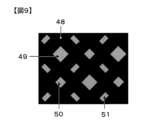
- a layer (A) having a hole-patterned opening having an opening area of 30.0 to 260.0 ⁇ m 2 in which light-emitting pixels are arranged in the display portion, which is given as a specific example of the embodiment of the present invention. indicates A layer (A) having a square pattern opening with an opening area in the range of 30.0 to 260.0 ⁇ m 2 in which light-emitting pixels are arranged in the display portion, which is given as a specific example of the embodiment of the present invention.
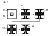
- FIG. 1 shows a manufacturing process of an organic EL display including a process of forming a pixel dividing layer in all examples and comparative examples.
- a numerical range represented using “to” means a range including the numerical values described before and after “to” as lower and upper limits.
- a pixel division layer means a pixel division layer provided in an organic EL display device, and does not include a black matrix of a liquid crystal display device.
- Visible light means light with a wavelength of 380 nm or more and less than 780 nm
- near-ultraviolet means light with a wavelength of 200 nm or more and less than 380 nm.
- the term “light shielding” refers to the ability to reduce the intensity of transmitted light compared to the intensity of light incident on the cured film in the vertical direction, and the term “light shielding property” refers to the extent to which visible light is shielded.
- a photosensitive composition means a composition having sensitivity to near-ultraviolet rays.
- the weight average molecular weight (Mw) means a value analyzed by gel permeation chromatography using tetrahydrofuran as a carrier and converted using a standard polystyrene calibration curve.
- the solid content means the ratio (% by weight) of components excluding solvent and water in the photosensitive composition.
- Color Index Generic Name used in the names of some coloring materials is an abbreviation for Color Index Generic Name, and based on the Color Index published by The Society of Dyers and Colorists, regarding coloring materials registered in the Color Index , Color Index Generic Name represents the chemical structure and crystal form of a pigment or dye.
- a negative type photosensitive containing a pigment and / or dye, a compound having two or more ethylenically unsaturated double bond groups in the molecule, and a photopolymerization initiator
- an opening with a narrow opening width for example, a square with a vertical width of 7.0 ⁇ m and a horizontal width of 7.0 ⁇ m
- an opening with a wide opening width for example, a vertical width of 30.0 ⁇ m and a horizontal width of 30 ⁇ m
- the light emission reliability of the finally obtained organic EL display device was found to be inferior.
- the present inventors have made intensive studies, conceived of combining a layer containing a cured product of a negative photosensitive composition and a layer containing a cured product of a positive photosensitive composition, It has been found that adopting the following configuration produces a particularly remarkable effect in solving the above-mentioned problems.
- the present invention provides an organic EL display device comprising a substrate, a planarizing layer, a first electrode, a pixel division layer, a luminescent pixel, and a second electrode in this order, wherein the pixel division layer comprises a layer (A) and a layer (B), wherein the layer (A) is a layer arranged on the surface of the first electrode with the surface of the first electrode partially exposed, and the layer (B) is the layer (A ) is a layer arranged on at least part of the surface of the layer (A), the layer (A) comprises a pigment and / or dye, a compound having two or more ethylenically unsaturated double bond groups in the molecule, and photopolymerization initiation a cured product of a negative photosensitive composition (a) containing an agent, and the layer (B) contains a cured product of a positive photosensitive composition (b) containing a resin and a photoacid generator It is an organic EL display device containing.
- An organic EL display device of the present invention comprises a substrate, a planarizing layer, a first electrode, a pixel dividing layer, a luminescent pixel and a second electrode in this order.
- FIG. 1 shows a cross-sectional view of a TFT substrate in an organic EL display device that is given as a specific example of an embodiment of the present invention.
- Bottom-gate type or top-gate type TFTs 1 are provided in a matrix on the surface of a substrate 6, and a TFT insulating layer 3 is formed to cover the TFTs 1 and wiring 2 connected to the TFTs 1.
- the TFT 1 include TFTs made of oxide semiconductors such as In--Ga--Zn--O (IGZO) and Ga--Zn--Sn, and low temperature polysilicon (LTPS).
- IGZO In--Ga--Zn--O
- LTPS low temperature polysilicon
- a flattening layer 4 is formed on the surface of the TFT insulating layer 3 , and a contact hole 7 for opening the wiring 2 is provided in the flattening layer 4 .
- the contact hole 7 may be, for example, a circular opening.
- a first electrode 5 is patterned on the surface of the planarizing layer 4 and connected to the wiring 2 .
- the layer (A) 8 is arranged on the surface of the first electrode 5 with the surface of the first electrode 5 partially exposed, and the layer (B) 9 is part of the surface of the layer (A) 8.
- Layer (A) 8 and layer (B) 9 form a pixel dividing layer 10 .
- the pixel division layer 10 is provided with openings, and light-emitting pixels 11 containing an organic EL light-emitting material are formed in the openings. and the light-emitting pixels 11 .
- the shape of the opening of the pixel division layer 10 is not particularly limited, and may be square, rectangular, perfect circle, or elliptical. is determined by the aperture width of By applying a voltage to the light-emitting pixel portion after sealing the TFT substrate having the above laminated structure under vacuum, it is possible to emit light as an organic EL display device.
- the organic EL display device of the present invention may be a bottom emission type organic EL display device in which emitted light emitted from the light emitting pixel 11 is taken out to the substrate side through the substrate 6, and the light is emitted through the second electrode 12. It may be a top-emission organic EL display device in which light is extracted to the opposite side of the substrate 6, and is not particularly limited.
- a rigid plate-shaped substrate such as glass is used as the substrate 6, a rigid type organic EL display device that cannot be bent can be obtained.
- the glass an alkali-free glass having an alkali metal element content of less than 0.5% and containing silicon as a main component can be suitably used. Among them, those having a small coefficient of thermal expansion and excellent dimensional stability in high-temperature processes at 250° C. or higher are preferred. 100 (manufactured by Asahi Glass Co., Ltd.), and its thickness is usually 0.1 to 0.5 mm from the viewpoint of physical durability.
- a bendable flexible organic EL display device can be obtained.
- a substrate made of a polyimide resin having high flexibility and excellent mechanical strength can be suitably used.
- a method of applying and then heating to imidize the polyamic acid to convert it into a polyimide resin, and then peeling off the temporary support with a laser or the like can be used.
- Polyamic acid can be synthesized by reacting a tetracarboxylic dianhydride and a diamine compound in an amide solvent such as N-methyl-2-pyrrolidone.
- a polyamic acid having an aromatic tetracarboxylic dianhydride residue and an aromatic diamine compound residue is preferred because of its superiority.
- a specific example is a polyamic acid having a residue of 3,3′,4,4′-biphenyltetracarboxylic dianhydride and a residue of p-phenylenediamine. Its thickness is usually 10 to 40 ⁇ m, and the thickness of the substrate 6 can be reduced as compared with the case of using non-alkali glass.
- the planarizing layer 4 is not particularly limited as long as it is a layer that functions as an insulating layer arranged as a base layer of the first electrode 5, and is formed so as to cover the convex portion caused by the thickness of the TFT 1, It may be a layer that functions to allow 5 to be patterned more smoothly.
- the planarizing layer 4 can be patterned using, for example, the same photosensitive composition as the negative photosensitive composition (a) or the positive photosensitive composition (b), which will be described later. It may consist of a single layer or two or more layers.
- the first electrode 5 may be made of any material as long as it is a film that functions as an anode electrode.
- conductive metal oxides such as ITO (Indium Tin Oxide), ITZO (Indium Tin Zinc Oxide), and IZO (Indium Zinc Oxide) can be used.
- ITO can be preferably used because of its excellent properties.
- As a method for patterning the ITO first, an ITO film is formed on the entire surface by a sputtering method, and then a positive resist material for etching is patterned by a photolithography method to obtain a resist pattern on the ITO film.
- the ITO referred to here includes so-called amorphous ITO.
- a positive resist material for etching a positive photosensitive composition containing an alkali-soluble novolac resin can be used.
- an aqueous solution containing nitric acid and hydrochloric acid or an aqueous oxalic acid solution can be used.
- IS-3 both of which are manufactured by Sasaki Chemicals Co., Ltd.).
- the first electrode 5 has a transparent conductive layer laminated on the surface of the metal reflective layer in order to improve the light extraction efficiency and the light emission luminance. It is preferably a laminated film, and may have, for example, a laminated structure of silver alloy/ITO or ITO/silver alloy/ITO. Examples of silver alloys include an alloy of Ag and Cu and an alloy of Ag, Pd and Cu.
- the luminescent pixel 11 is not particularly limited, and the emitted light may have any peak wavelength.
- the organic EL light-emitting material constituting the light-emitting pixel 11 a material obtained by combining a hole-transporting layer and/or an electron-transporting layer in addition to the light-emitting layer can be preferably used.
- Examples of light emitting pixels of each color include red light emitting pixels with a peak wavelength of 560 to 700 nm, blue light emitting pixels with a peak wavelength of 420 to 490 nm, and green light emitting pixels with a peak wavelength of 500 to 550 nm.
- a method of performing vapor deposition by contacting a vapor deposition mask having openings in a desired pattern shape there is a method of performing vapor deposition by contacting a vapor deposition mask having openings in a desired pattern shape.
- a vapor deposition mask that can be used to form the high-definition light-emitting pixels 11 for example, the vapor deposition mask disclosed in Japanese Patent Application Laid-Open No. 2019-163543 can be mentioned.
- the second electrode 12 may be made of any material as long as it is a film that functions as a cathode electrode.
- a layer made of an alloy of silver and magnesium is used in terms of high light transmittance and excellent light extraction efficiency. It can be preferably used. It is preferable to form a thin film so that the layer has a higher light transmittance in the visible region than the first electrode 5 described above.
- a layer made of an aluminum alloy can be preferably used in terms of high light reflectivity and excellent light extraction efficiency, and is visible compared to the first electrode 5 described above. It is preferable to form a thick film so that the layer has a high light reflectance in the region.
- the second electrode 12 can be formed by depositing a film on the entire surface by a sputtering method.
- the organic EL display device of the present invention may further comprise a color filter substrate comprising at least one color filter and a substrate.
- a color filter substrate comprising at least one color filter and a substrate.
- a color filter substrate the cross section of which is shown in FIG. 2
- the light extraction side is the light emitting surface side of the organic EL display device.
- the organic EL display device is a bottom emission type organic EL display device that extracts light emitted from the light emitting pixels 11 through the substrate 6 to the substrate side
- the light extraction side is the substrate side.
- the organic EL display device is a top emission type organic EL display device in which emitted light is extracted to the opposite side of the substrate 6 via the second electrode 12
- the light extraction side is the opposite side of the substrate 6 . That is, it is preferable that the organic EL display device of the present invention further include a color filter on the light extraction side of the light-emitting pixels.
- a green color filter 15 , a red color filter 16 and a blue color filter 17 are patterned in the openings of the black matrix 14 arranged on the surface of the substrate 13 .
- the opening width/shape of the openings of the black matrix 14 may be the same as or different from the opening width/shape of the openings of the layer (A) in FIG.
- the color filter substrate may be highly flexible, and a thermosetting or near-ultraviolet curable transparent adhesive or the like can be easily applied to the surface of the substrate 6 or the surface of the second electrode 12 in FIG. Can be pasted together.
- transparent adhesives include “Structbond” (registered trademark) (manufactured by Mitsui Chemicals, Inc.).
- the pixel division layer 10 will be described in detail as follows.
- the pixel division layer included in the organic EL display device of the present invention includes layer (A) and layer (B).
- the layer (A) is a layer arranged on the surface of the first electrode with the surface of the first electrode partially exposed, and the layer (B) is at least part of the surface of the layer (A) It is a layer arranged in That is, the pixel division layer provided in the organic EL display device of the present invention is a laminated film composed of a plurality of layers.
- the layer (A) is a layer arranged on the surface of the first electrode with the surface of the first electrode partially exposed means that the layer (A) is arranged only on the surface of the first electrode It means that it may be a layer, or it may be a layer arranged on the surface of the first electrode and on the surface of another layer other than the first electrode.
- a configuration in which the layer (A) is a layer arranged on the surface of the first electrode and the surface of the planarizing layer is preferably mentioned.
- the structure in which the layer (B) is arranged on at least part of the surface of the layer (A) has the effect of improving the light emission reliability of the organic EL display device. Desirably high light emission reliability regardless of the resolution of the layer (A) due to the structure in which the layer (B) containing the cured product of the positive photosensitive composition (b) containing a resin and a photoacid generator is laminated can be obtained.
- high light emission reliability means that the area ratio of the light emitting portion to the area of the light emitting pixel portion of the organic EL display device (pixel light emitting area ratio) is kept high, that is, the generation of non-light emitting portions due to pixel shrinkage is prevented. means less.
- the higher the light emission reliability the longer the light emission life, and the higher the value as a display device because it can be used while maintaining high luminance over a long period of time.
- the area of the non-light-emitting portion which tends to progress gradually from the periphery of the light-emitting pixel portion toward the central portion, tends to increase as the size of the light-emitting pixel decreases.
- the smaller the light-emitting pixel size the greater the change in the pixel light-emitting area ratio per 1.0 ⁇ m 2 of the area of the non-light-emitting portion.
- the unreacted portion and / or decomposed product of the photopolymerization initiator, etc. remain inside the film of the layer (A), and at least the effect of suppressing the release into the light emitting device contributed. It is considered to be a thing.
- the aspect of the pixel division layer in which the layer (B) is arranged on at least part of the surface of the layer (A) is not particularly limited, a specific example of a preferred embodiment of the organic EL display device of the present invention is shown in FIG. 3 to 7. In the plane of the display portion of the organic EL display device, these different pixel division layer modes may be mixed.
- the display portion of the organic EL display device means a region where the user of the organic EL display device recognizes the light emitted from the light-emitting pixels on the light extraction side when the organic EL display device is driven.
- the content displayed by the display unit is not particularly limited, and includes, for example, character information, images, and moving images.
- a decorative portion such as a bezel portion in which light-emitting pixels are not arranged is not included in the display portion.
- the pixel division layer included in the organic EL display device of the present invention preferably has a stepped shape and a spacer function.
- a spacer function By having a spacer function, the contact area between the pixel dividing layer and the vapor deposition mask can be reduced when forming the light-emitting pixels, chipping and damage can be prevented, and the production yield can be improved.
- the area where the layer (A) and the layer (B) are in contact is the layer (A ) of the total surface area, preferably 5% or more, more preferably 20% or more. That is, in the display portion of the organic EL display device of the present invention, the area ratio of the layer (B) covering the surface of the layer (A) is 20 to 100% in 100% of the total surface area of the layer (A). It is preferable to have a certain site.
- the area ratio of the layer (B) covering the surface of the layer (A) is the area of the layer (B) covering the surface of the layer (A) in a randomly selected square area of 250 ⁇ m long and 250 ⁇ m wide in the display area.
- the optical density per 1.0 ⁇ m film thickness of the layer (A) is preferably 0.5 or more, more preferably 0.7, in terms of improving the effect of suppressing reflection of external light and improving light emission reliability.
- the above is more preferable.
- it is preferably 1.5 or less, more preferably 1.4 or less, in order to improve light emission reliability. That is, the optical density (OD/ ⁇ m) per 1.0 ⁇ m film thickness of the layer (A) included in the pixel dividing layer included in the organic EL display device of the present invention is preferably 0.5 to 1.5.
- the optical density per 1.0 ⁇ m film thickness of the layer (B) is preferably 0.3 or less, more preferably 0.1 or less, in order to improve light emission reliability. That is, the optical density (OD/ ⁇ m) per 1.0 ⁇ m film thickness of the layer (B) included in the pixel division layer included in the organic EL display device of the present invention is preferably 0.0 to 0.3.
- the optical density per 1.0 ⁇ m film thickness as used herein is calculated by measuring the incident light intensity and the transmitted light intensity using an optical densitometer (manufactured by X-Rite; X-Rite 361T) and calculating from the following formula. It means the value obtained by dividing the value obtained by dividing the value by the value of the film thickness and rounding off to the second decimal place, and the higher the optical density, the higher the light shielding property.
- the maximum thickness of the layer (A) is 0.5 ⁇ m in order to improve the light shielding property. 0.8 ⁇ m or more is more preferable.
- the thickness is preferably 3.0 ⁇ m or less, more preferably 2.0 ⁇ m or less, in order to improve light emission reliability.
- the maximum thickness of the layer (B) is preferably 0.1 ⁇ m or more, more preferably 0.3 ⁇ m or more, in order to improve light emission reliability. more preferred.
- the thickness is preferably 3.0 ⁇ m or less, more preferably 2.0 ⁇ m or less, in order to improve light emission reliability. That is, in the organic EL display device of the present invention, the maximum thickness of the layer (A) is 0.5 to 3.0 ⁇ m at the portion where the layer (B) is arranged on the surface of the layer (A), Moreover, it is preferable that the layer (B) has a portion where the maximum value of the film thickness is 0.1 to 3.0 ⁇ m.
- the maximum value of the film thickness of the layer (A) and the maximum value of the film thickness of the layer (B) are within a randomly selected area of 250 ⁇ m long/250 ⁇ m wide in the display section of the organic EL display device.
- Each of the values obtained by measuring the maximum film thickness of the layer (A) and the maximum film thickness of the layer (B) can be rounded off to the second decimal place for calculation.
- the film thicknesses of the layer (A) and the layer (B) can be measured by observing the cross section of the pixel division layer using a scanning electron microscope (hereinafter referred to as "SEM") and taking the image.
- SEM scanning electron microscope
- the portions (A) and (B) are mixed or welded together to form an intermediate layer on the surface where the layer (A) and the layer (B) are in contact, the portion corresponding to the center of the intermediate layer in the film depth direction is the layer (A) ) and the layer (B), and the film thickness can be measured respectively.
- SEM scanning electron microscope
- the cross-sectional taper angle of the end portion of the pixel division layer at the boundary with the opening of the pixel division layer is preferably 50° or less, and 40°, in order to improve the film-forming properties of the second electrode and suppress non-lighting of the light-emitting pixel.
- the angle is preferably 15° or more, and more preferably 20° or more, in order to improve the light-shielding properties of the ends of the openings of the pixel division layer.
- both layers are preferably arranged so that the opening width of the opening of the layer (A) is the same as or narrower than the opening width of the opening of the layer (B). That is, it is preferable that the end portions of the openings of the pixel dividing layer have a light-shielding property derived from the layer (A).
- the layer (A) has an opening having an opening area of 30.0 ⁇ m 2 or more in which light emitting pixels are arranged in the display portion.
- each opening is not particularly limited, and may be, for example, a perfect circular opening with a diameter of 7 to 18 ⁇ m or a square opening with a side of 6 to 16 ⁇ m.
- Layer (A) is a negative photosensitive composition (a) containing a pigment and/or dye, a compound having two or more ethylenically unsaturated double bond groups in the molecule, and a photopolymerization initiator. It contains a cured product as an essential component. A film containing a cured product is sometimes referred to as a cured film. The content of the cured product of the negative photosensitive composition (a) is preferably 99% by weight or more in the layer (A) in order to improve light emission reliability.
- a negative-working photosensitive composition is a composition obtained by making the alkali-solubility of a film in an exposed area relatively lower than the alkali-solubility of a film in an unexposed area by pattern exposure through a negative-type exposure mask. It means a composition having negative photosensitivity that forms a pattern by removing an unexposed portion of the film with a developer.
- the layer (B) contains as an essential component a cured product of the positive photosensitive composition (b) containing a resin and a photoacid generator.
- a film containing a cured product is sometimes referred to as a cured film.
- the content of the cured product of the positive photosensitive composition (b) is preferably 99% by weight or more in the layer (B) in order to improve light emission reliability.
- a positive photosensitive composition is an alkali-developable composition in which the alkali solubility of the film in the exposed area is made relatively higher than the alkali solubility of the film in the unexposed area by pattern exposure through a positive exposure mask. It means a composition having positive photosensitivity that removes the film in the exposed area with a liquid to form a pattern.
- the cured product of the negative photosensitive composition (a) as used herein refers to a method comprising at least a step of heat-treating the negative photosensitive composition (a) at a heating temperature of 200° C. or higher for 10 minutes or longer. It means what you get.
- the cured product of the positive photosensitive composition (b) is obtained by a method including at least the step of heat-treating the positive photosensitive composition (b) at an actual temperature of 200° C. or higher for 10 minutes or longer. means things.
- the layer (A) contains the cured product of the negative photosensitive composition (a) as an essential component
- the layer (B) contains the cured product of the positive photosensitive composition (b) as an essential component.
- Other components may be contained within a range that does not impair the technical effects of the invention.
- Other components include, for example, water adsorbed to the cured product of the negative photosensitive composition (a) or the cured product of the positive photosensitive composition (b).
- the total amount of other components in layer (A) or layer (B) is preferably 1% by weight or less.
- the negative photosensitive composition (a) contains pigments and/or dyes. By containing a pigment and/or a dye, the layer (A) can be provided with a light-shielding property.
- a benzodifuranone-based black pigment is preferable from the viewpoint of excellent light shielding properties and light emission reliability.
- a benzodifuranone-based black pigment is an organic black pigment composed of a compound having one polycyclic structure in which two furanone rings are condensed to one benzene ring in the molecule, and is described, for example, in WO 2009/010521. Bis-oxodihydroindolylene-benzodifuranones are mentioned.
- the cured product of the negative photosensitive composition (a) contains a benzodifuranone-based black pigment represented by the formula (1) or (2) in order to improve the light emission reliability. It is more preferable that the cured product of the negative photosensitive composition (a) contains a benzodifuranone-based black pigment represented by formula (3).
- R 1 to R 10 in formula (1) are hydrogen atoms.
- Commercially available benzodifuranone-based black pigments represented by formula (3) include Irgaphor Black (registered trademark) S0100CF and Experimental Black 582 (both of which are manufactured by BASF).
- the benzodifuranone-based black pigment represented by formula (1) or formula (2) has a coating layer containing silica, metal oxides and/or metal hydroxides to improve the pigment surface. At least a portion is preferably covered.
- the cured product of the negative photosensitive composition (a) further contains a compound represented by formula (4) or a salt thereof.
- R 1 to R 10 each independently represent a hydrogen atom, a fluorine atom, an alkyl group having 1 to 12 carbon atoms, a hydroxyl group or a carboxyl group.
- At least one perylene organic pigment selected from the group consisting of 3,4,9,10-perylenetetracarboxylic acid bisbenzimidazole is preferably contained. More preferably, it contains 3,4,9,10-perylenetetracarboxylic acid bisbenzimidazole.
- the cured product of the negative photosensitive composition (a) contained in the layer (A) included in the organic EL display device of the present invention further contains 3,4,9,10-perylenetetracarboxylic acid bisbenzimidazole It is more preferable to contain
- the 3,4,9,10-perylenetetracarboxylic acid bisbenzimidazole is a cis compound represented by the formula (5) and a trans compound represented by the formula (6).
- the cured product of the negative-type photosensitive composition (a) can contain the above-described perylene-based organic pigment.
- pigments for example, C.I. I. Pigment Yellow 151, 175, 180, 185, 192, C.I. I. Pigment Red 254, 255, 264, C.I. I. Pigment Orange 43, 61, 72, C.I. I. Pigment Blue 15:3, 15:4, 15:6, 25, 26, 60, 65, 80, C.I. I.
- Organic pigments such as Pigment Violet 19, 29, 32 and 37, and inorganic pigments such as carbon black, titanium nitride and zirconium nitride may be used in combination.
- oil-soluble dyes and acid dyes are preferable from the viewpoint of solubility in solvents and developability, such as C.I. I. Solvent Red 46, 72, C.I. I. Red dyes such as Acid Red 52, 87, 289, 388, C.I. I. yellow dyes such as Solvent Yellow 93, C.I. I. Solvent Blue 35, 45, 97, 104, 122, C.I. I. blue dyes such as Acid Blue 9, 25, 27, 40, 80, 90, 112, 127, 129, 145, C.I. I. solvent violet 9, 13, 43, C.I. I. violet dyes such as Acid Violet 29, 31, 33, 36, 39, 48, 63, 109; I. Solvent Black 27, 29, 34, C.I. I. Black dyes such as Acid Black 52 are included. If necessary, the acid dye may be salt-formed with a basic dye or a cationic component to improve the solubility in a solvent.
- Pigments and dyes may be contained in the negative photosensitive composition (a), and the total content thereof is the same as that of the negative photosensitive composition in order to achieve both light shielding properties and resolution of the layer (A). It is preferably 10 to 50% by weight based on 100% by weight of solid content.
- the above-mentioned organic pigments and dyes are near-infrared transmissive, and using a near-infrared camera, high-precision automatic alignment between the substrate on which the prebaked film is formed and the exposure mask, that is, near-infrared alignment is possible. Yield during production can be improved.
- the negative photosensitive composition (a) contains a compound having two or more ethylenically unsaturated double bond groups in the molecule.
- a compound having two or more ethylenically unsaturated double bond groups in the molecule undergoes a photocuring reaction chained by radical active species generated by a photopolymerization initiator, which will be described later.
- the alkali solubility of the unexposed portion of the film is relatively lower than that of the film, and pattern formation by negative photolithography becomes possible.
- a compound having two or more ethylenically unsaturated double bond groups in the molecule and corresponding to an alkali-soluble resin described later has two or more ethylenically unsaturated double bond groups in the molecule. It is defined as a component belonging to a compound having
- the content of the compound having two or more ethylenically unsaturated double bond groups in the molecule is 100% by weight of the solid content of the negative photosensitive composition in order to achieve both film adhesion and resolution in the development process. 10 to 60% by weight is preferred.
- R 34 and R 35 each independently represent a hydrogen atom or a methyl group. * represents a bonding site with a carbon atom.
- R 36 represents a tetravalent organic group containing an aromatic ring or cycloaliphatic.
- R37 represents a trivalent organic group containing an aromatic ring or cycloaliphatic.
- R 38 represents an alkylene group having 1 to 5 carbon atoms.
- R39 represents a hydrogen atom or a methyl group. * represents a binding site.
- the negative photosensitive composition (a) contains a photopolymerization initiator.
- the photopolymerization initiator is not particularly limited as long as it is a compound that generates radical active species upon exposure to near-ultraviolet rays.
- Examples of photopolymerization initiators include oxime ester photopolymerization initiators, alkylphenone photopolymerization initiators, and acylphosphine oxide photopolymerization initiators. Among them, oxime ester-based photopolymerization initiators are preferable for improving the adhesion of the film in the development process. ), "Irgacure" (registered trademark) OXE01, OXE02, OXE03, OXE04, and compounds represented by formula (9).
- the content of the photopolymerization initiator is preferably 1 to 10% by weight based on 100% by weight of the solid content of the negative photosensitive composition in order to achieve both film adhesion and resolution in the development process.
- the negative photosensitive composition (a) preferably further contains an alkali-soluble resin in order to improve the resolution of the layer (A).
- the alkali-soluble resin referred to here means that a solution obtained by dissolving the resin in ⁇ -butyrolactone is applied to the surface of a silicon wafer and prebaked on a hot plate at an actual temperature of 120° C. for 4 minutes to obtain a film thickness of 10 ⁇ 0.5 ⁇ m.
- the pre-baked film is immersed in a 2.38% by weight tetramethylammonium hydroxide aqueous solution at 23 ⁇ 1 ° C., which is an alkaline developer, for 1 minute, and then in pure water at 23 ⁇ 1 ° C. for 10 seconds.
- a resin is a compound having a weight average molecular weight (Mw) of 1000 or more and having a polymer chain composed of repeating structural units.
- Alkali-soluble resins include, for example, alkali-soluble phenolic resins, alkali-soluble (meth)acrylic resins, alkali-soluble polyhydroxystyrenes, alkali-soluble polyimides, alkali-soluble polyimide precursors, alkali-soluble polybenzoxazoles, and alkali-soluble polybenzoxazole precursors. , alkali-soluble polysiloxane, and alkali-soluble polyamine. You may use these individually or in mixture.
- the alkali-soluble polyimide precursor as used herein means a resin that forms an imide bond by heat treatment and is converted into a polyimide, and specific examples thereof include polyamic acid and polyamic acid ester.
- alkali-soluble phenol resin an alkali-soluble (meth)acrylic resin and/or an alkali-soluble polyimide in order to reduce the cross-sectional taper angle of the end of the layer (A) and improve the resolution.
- alkali-soluble polyamine as a pigment dispersant.
- (Meth)acrylic resin means methacrylic resin or acrylic resin. Examples of alkali-soluble phenolic resins include novolak-type phenolic resins, resol-type phenolic resins, and novolac-type phenolic resins having a polymer chain made of polyhydroxystyrene described in JP-A-2010-106278, and known methods.
- alkali-soluble polyamines include resins having two or more tertiary amino groups in the molecule described in Patent Document 1.
- Alkali-soluble polyimides include resins having a structural unit represented by formula (10) described later.
- the negative photosensitive composition (a) may further contain a solvent.
- a solvent By containing a solvent, the viscosity, thixotropy, etc. of the negative photosensitive composition can be adjusted, and the film thickness uniformity of the coating film can be enhanced.
- solvents include propylene glycol monomethyl ether (hereinafter referred to as PGME), propylene glycol monoethyl ether, dipropylene glycol monomethyl ether, propylene glycol monomethyl ether acetate (hereinafter referred to as "PGMEA”), 3 -Methoxybutyl acetate (hereinafter referred to as "MBA”), methyl lactate, ethyl lactate, ⁇ -butyrolactone, valerolactone, and ⁇ -caprolactone are preferred.
- PGME propylene glycol monomethyl ether
- PGMEA propylene glycol monoethyl ether
- MFA 3 -Methoxybutyl acetate
- the water content in 100 parts by weight of the negative photosensitive composition (a) is preferably 0.01 to 0.5 parts by weight.
- a leveling agent consisting of a nonionic surfactant may be contained in order to obtain a higher film thickness uniformity.
- the cured product of the negative photosensitive composition (a) contained in the layer (A) has a primary particle diameter of 5 to 30 nm and an aspect ratio (major axis/minor axis) of It preferably contains 1.0 to 1.5 silica particles.
- the silica particles referred to here are particles with a pure content of SiO2 of 90% by weight or more in the weight excluding water, particles made of silicon dioxide (anhydrous silicic acid), silicon dioxide hydrate (hydrous silicic acid, white It means particles made of carbon) or particles made of quartz glass. Also included are particles of orthosilicic acid, metasilicic acid and/or metadisilicic acid.
- the structure of the particles is not particularly limited, and they may have internal voids.
- the aspect ratio as used herein means a value obtained by dividing the length of the silica particles by the length of the silica particles and rounding off to the second decimal place.
- the aspect ratio when the aspect ratio is 1.0, it can be regarded as spherical silica particles.
- Silica particles having a primary particle diameter of 5 to 30 nm and an aspect ratio (major axis/minor axis) of 1.0 to 1.5 or a dispersion containing the silica particles are contained in the negative photosensitive composition (a). This allows the silica particles to be contained in the cured product of the negative photosensitive composition (a).
- dispersions containing silica particles having a primary particle diameter of 5 to 30 nm and an aspect ratio (major axis/minor axis) of 1.0 to 1.5 include MEK-ST-40 and MEK-ST- L (both of which are manufactured by Nissan Chemical Industries, Ltd.).
- the primary particle size and aspect ratio were measured by using a transmission electron microscope (TEM) on a cross section that was polished by ion milling to improve smoothness, using a thinly cut pixel division layer as an observation sample.
- TEM transmission electron microscope
- An image analysis type particle size distribution measuring machine "Mac-View” (manufactured by MOUNTECH) was used to capture an image of a point located in the range of 0.2 to 0.8 ⁇ m in the film depth direction from the surface layer at a magnification of 50000 times. can be measured using Furthermore, by energy dispersive X-ray spectroscopy (TEM-EDX), silica particles can be specified by determining the elements that constitute the particles.
- Mac-View manufactured by MOUNTECH
- the negative photosensitive composition (a) may further contain a thermal cross-linking agent.
- a thermal cross-linking agent By containing an appropriate amount of the thermal cross-linking agent within a range that does not impair the resolution, it may be possible to obtain higher light emission reliability.
- the thermal cross-linking agent compounds having two or more epoxy groups are preferred, and specific examples include TEPIC-L, TEPIC-S, TEPIC-PAS (all of which are manufactured by Nissan Chemical Industries, Ltd.), NC-3000, XD-1000 and XD-1000H (both of which are manufactured by Nippon Kayaku Co., Ltd.).
- the positive photosensitive composition (b) contains a resin.
- the resin is not particularly limited, examples thereof include the aforementioned alkali-soluble resins.
- the cured product of the positive photosensitive composition (b) contained in the layer (B) preferably contains a resin having an imide bond and/or a benzoxazole skeleton.
- a resin having an imide bond and/or a benzoxazole skeleton or a precursor thereof in the positive photosensitive composition (b) the imide bond is formed in the cured product of the positive photosensitive composition (b). and/or a resin having a benzoxazole skeleton can be contained.
- the positive photosensitive composition (b) is an alkali-soluble polyimide, an alkali-soluble polyimide precursor, an alkali-soluble polybenzoxazole, an alkali-soluble polybenzoxazole precursor and/or It is preferable to contain a copolymer of It is more preferable to contain a resin having a structural unit represented by formula (10) and/or a structural unit represented by formula (11).
- R 11 represents a 4- to 10-valent organic group.
- R 12 represents a divalent to octavalent organic group.
- R 13 and R 14 each independently represent a phenolic hydroxyl group or a carboxyl group, each of which may be a single group or a mixture of different groups.
- p and q are integers and each independently represents 0-6. However, p+q>0 is satisfied. * represents a binding site.
- R 15 and R 16 represent divalent to octavalent organic groups.
- R 17 and R 18 each independently represent a hydroxyl group, a carboxyl group or COOA, and each may be a single group or a mixture of different groups.
- A represents a monovalent hydrocarbon group having 1 to 10 carbon atoms.
- r and s are integers and each independently represent 0-6. However, r+s>2 is satisfied.
- * represents a binding site.
- examples of the monovalent hydrocarbon group A having 1 to 10 carbon atoms include a methyl group, an ethyl group, a propyl group, a phenyl group and a benzyl group.
- the weight average molecular weight (Mw) of the resin having the structural unit represented by formula (10) and/or the structural unit represented by formula (11) is 10,000 or more and 50,000 or less for improving resolution. is preferred.
- R19 represents a single bond, an oxygen atom, C( CF3 ) 2 , C( CH3 ) 2 or SO2 .
- R20 and R21 each independently represent a hydrogen atom or a hydroxyl group.
- R 15 -(R 17 )r represents an acid residue.
- R 15 is preferably an organic group having 5 to 40 carbon atoms containing an aromatic ring or cycloaliphatic group.
- acid residues include dicarboxylic acid residues, tricarboxylic acid residues, and tetracarboxylic acid residues.
- Dicarboxylic acids include terephthalic acid, isophthalic acid, diphenyletherdicarboxylic acid, bis(carboxyphenyl)hexafluoropropane, biphenyldicarboxylic acid, benzophenonedicarboxylic acid, and triphenyldicarboxylic acid.
- Tricarboxylic acids include residues of trimellitic acid, trimesic acid, diphenylethertricarboxylic acid, biphenyltricarboxylic acid.
- Tetracarboxylic acid residues include pyromellitic acid, 3,3′,4,4′-biphenyltetracarboxylic acid, 2,3,3′,4′-biphenyltetracarboxylic acid, 2,2′,3, 3′-biphenyltetracarboxylic acid, 3,3′,4,4′-benzophenonetetracarboxylic acid, 2,2′,3,3′-benzophenonetetracarboxylic acid, 2,2-bis(3,4-dicarboxy phenyl)hexafluoropropane, 2,2-bis(2,3-dicarboxyphenyl)hexafluoropropane, 1,1-bis(3,4-dicarboxyphenyl)ethane, 1,1-bis(2,3- dicarboxyphenyl)ethane, bis(3,4-dicarboxyphenyl)methane, bis(2,3-dicarboxyphenyl)methane, bis(3,
- R 12 -(R 14 )q in formula (10) and R 16 -(R 18 )s in formula (11) represent diamine residues.
- R 12 and R 16 are preferably C 5-40 organic groups containing an aromatic ring or a cycloaliphatic group.
- Diamine residues include, for example, 3,4′-diaminodiphenyl ether, 4,4′-diaminodiphenyl ether, 3,4′-diaminodiphenylmethane, 4,4′-diaminodiphenylmethane, 1,4-bis(4-amino phenoxy)benzene, m-phenylenediamine, p-phenylenediamine, 1,5-naphthalenediamine, 2,6-naphthalenediamine, bis(4-aminophenoxy)biphenyl, bis ⁇ 4-(4-aminophenoxy)phenyl ⁇ ether , 1,4-bis(4-aminophenoxy)benzene, 2,2′-dimethyl-4,4′-diaminobiphenyl, 2,2′-diethyl-4,4′-diaminobiphenyl, 3,3′-dimethyl -4,4'-diaminobiphenyl, 3,3'-
- R22 represents a single bond, an oxygen atom, C( CF3 ) 2 , C( CH3 ) 2 or SO2 .
- R23 and R24 each independently represent a hydrogen atom or a hydroxyl group.
- R25 represents a single bond, an oxygen atom, C( CF3 ) 2 , C( CH3 ) 2 or SO2 .
- R26 and R27 each independently represent a hydrogen atom or a hydroxyl group.
- R 28 , R 29 , R 30 and R 31 each independently represent a hydrogen atom or a hydroxyl group.
- R 32 and R 33 each independently represent a hydrogen atom or a hydroxyl group.
- the weight average molecular weight (Mw) can be easily adjusted during synthesis, and the storage stability as an alkali-soluble resin can be improved.
- Examples of monoamines include 1-hydroxy-4-aminonaphthalene, 2-hydroxy-7-aminonaphthalene, 2-hydroxy-6-aminonaphthalene, 2-hydroxy-5-aminonaphthalene and 1-carboxy-7-aminonaphthalene. , 1-carboxy-6-aminonaphthalene, 1-carboxy-5-aminonaphthalene, 2-carboxy-7-aminonaphthalene, 2-carboxy-6-aminonaphthalene, 2-aminophenol, 3-aminophenol, 4-amino Phenol is mentioned.
- the group represented by COOA is obtained by converting the carboxyl group with an esterifying agent.
- Esterifying agents include, for example, N,N-dimethylformamide dimethylacetal and N,N-dimethylformamide diethylacetal.
- a resin having a structural unit represented by formula (10) and/or a structural unit represented by formula (11) can be obtained by a known method. 097992 and WO 2019/181782.
- the content of the resin is preferably 50 to 90% by weight based on 100% by weight of the solid content of the positive photosensitive composition (b) in order to improve light emission reliability.
- the positive photosensitive composition (b) contains a photoacid generator.
- the photoacid generator is not particularly limited as long as it is a compound that is decomposed by irradiation with near-ultraviolet light to generate an acid.
- the generated acid has the effect of making the alkali solubility of the film in the exposed area relatively higher than that of the film in the unexposed area, making it possible to form a pattern by positive photolithography.
- Examples of the generated acid include indenecarboxylic acid, methanesulfonic acid, ethanesulfonic acid, benzenesulfonic acid, p-toluenesulfonic acid, and naphthalenesulfonic acid.
- photoacid generators examples include quinonediazide compounds, imidosulfonate compounds, and oximesulfonate compounds.
- a quinonediazide compound that produces a carboxylic acid and/or a sulfonic acid as an acid by irradiation with near-ultraviolet light is preferable for improving light emission reliability.
- the quinonediazide compound is an esterification reaction of a compound having a phenolic hydroxyl group and 1,2-naphthoquinone-2-diazide-4-sulfonyl chloride (hereinafter sometimes referred to as "4-naphthoquinonediazide sulfonyl chloride").
- a 4-naphthoquinonediazide sulfonyl ester compound or a compound having a phenolic hydroxyl group, which is the resulting compound, and 1,2-naphthoquinone-2-diazide-5-sulfonyl chloride hereinafter referred to as "5-naphthoquinonediazide sulfonyl chloride"
- 5-naphthoquinonediazide sulfonyl chloride 1,2-naphthoquinonediazide sulfonyl chloride
- 5-naphthoquinonediazide sulfonyl ester compound which is a compound obtained by an esterification reaction of
- a naphthoquinonediazide sulfonic acid derivative described in JP-A-2019-174793.
- Examples of compounds having a phenolic hydroxyl group include TrisP-HAP, TrisP-PA, TekP-4HBPA, TrisP-SA, TrisOCR-PA, BisP-AP, BisP-NO, BisP-PR, BisP-B, and BisP-DE. , BisP-DP, BisP-DP, BisRS-2P, BisRS-3P, and BisP-DEK (all of which are manufactured by Honshu Chemical Industry Co., Ltd.).
- Commercially available 5-naphthoquinonediazide sulfonyl ester compounds include, for example, 4NT-250 and 4NT-300 (manufactured by Toyo Gosei Co., Ltd.).
- the content of the photoacid generator is preferably 1 to 40% by weight based on 100% by weight of the solid content of the positive photosensitive composition (b) in order to improve the exposure sensitivity.
- the positive photosensitive composition (b) may further contain a thermal cross-linking agent.
- a thermal cross-linking agent By containing a thermal cross-linking agent, more excellent light emission reliability can be obtained.
- a compound having two or more alkoxyalkyl groups in the molecule is preferable as the thermal cross-linking agent.
- Alkoxyalkyl groups include, for example, methoxymethyl, ethoxymethyl, propoxymethyl, and butoxymethyl groups.
- Preferred examples of the compound having two or more alkoxymethyl groups in the molecule include compounds represented by formula (17), compounds represented by formula (18), and compounds represented by formula (19). .
- the positive photosensitive composition (b) may further contain the aforementioned solvent.
- a solvent By containing a solvent, the viscosity, thixotropy, etc. of the positive photosensitive composition can be adjusted, and the film thickness uniformity of the coating film can be improved.
- the layer (B) may contain pigments and/or dyes in the same manner as the layer (A) as long as the effects of the present invention are not impaired.
- the total content of the pigment and dye is preferably 5 parts by weight or less, more preferably 0 parts by weight, based on 100 parts by weight of the layer (B) in order to obtain high light emission reliability.
- the organic EL display device of the present invention is an organic EL display device comprising a substrate, a planarization layer, a first electrode, a pixel division layer, a light emitting pixel, and a second electrode in this order, wherein the pixel division layer is a layer (A) and a layer (B), wherein the layer (A) is a layer disposed on the surface of the first electrode with the surface of the first electrode partially exposed, and the layer (B) is a layer arranged on at least a part of the surface of the layer (A), and the layer (A) is a compound having a pigment and/or dye and two or more ethylenically unsaturated double bond groups in the molecule and a cured product of a negative photosensitive composition (a) containing a photopolymerization initiator, and the layer (B) contains a resin and a photoacid generator. ), and the total content of pigments and/or dyes in the layer (B) is 5 parts by weight or less per 100 parts
- the method of forming the layer (A) using the negative photosensitive composition (a) includes a coating step of applying the negative photosensitive composition (a) to obtain a coating film, and a negative exposure mask.
- a method comprising a developing step of obtaining a developed film by heating and a curing step of thermosetting by heating to obtain a cured film is preferred.
- the method of forming the layer (B) using the positive photosensitive composition (b) includes a coating step of applying the positive photosensitive composition (b) to obtain a coating film, and a positive exposure mask.
- a spin coater or a slit coater can be preferably used as a coating device used in the coating process because of its excellent thin film coating properties.
- pin gap pre-baking or contact pre-baking may be performed.
- the prebaking temperature is preferably 50 to 150° C.
- the prebaking time is preferably 30 seconds to 5 minutes.
- Examples of exposure apparatuses used in the exposure process include steppers, mirror projection mask aligners (MPA), and parallel light mask aligners (PLA).
- Actinic rays including near-ultraviolet rays irradiated during exposure include j-line (wavelength 313 nm), i-line (wavelength 365 nm), h-line (wavelength 405 nm) or g-line (wavelength 436 nm) of a mercury lamp, i-line or , mixed lines including g-, h- and i-lines are preferred.
- Examples of negative exposure masks and positive exposure masks include masks in which a light shielding portion made of a metal such as chromium is formed in a pattern on one surface of a substrate having a near ultraviolet ray transmitting portion such as glass, quartz or film.
- An exposed film having an exposed portion and an unexposed portion in the plane can be obtained by performing pattern exposure by transmitting actinic radiation only through the opening portion.
- a halftone exposure mask having a full-transmissive portion and a semi-transmissive portion in the plane which have different transmittances for actinic rays, a convex thick-film portion is collectively formed to form a pixel.
- a spacer function may be imparted to at least part of the dividing layer.
- Examples of the developing method in the developing process include methods such as showering, dipping, and puddle, and include a method of immersing the exposed film for 10 seconds to 3 minutes.
- the paddle method is preferable for improving the in-plane uniformity of the opening width of the opening.
- TMAH tetramethylammonium hydroxide aqueous solution
- washing treatment by showering with deionized water and/or draining treatment by blowing air may be added.
- the developed film is thermally cured by heating, and at the same time, moisture and developer are volatilized.
- Heating devices include, for example, hot air ovens and IR ovens.
- the heating temperature is preferably 200 to 350°C, more preferably 220 to 280°C under atmospheric pressure.
- a pigment dispersion is prepared by a wet dispersion treatment, and then a compound having two or more ethylenically unsaturated double bond groups in the molecule and light. After mixing the polymerization initiator and, if necessary, other components such as a solvent, the mixture is added to the pigment dispersion, mixed and stirred, and optionally filtered using a filter.
- a wet media dispersing machine such as a bead mill because of its excellent dispersion treatment speed, strong crushing force, and economical advantage.
- the cumulative 50% particle size of the pigment in the pigment dispersion and in the negative photosensitive composition (a) prepared using the same is preferably 20 nm or more, and preferably 40 nm or more, in order to improve light emission reliability. more preferred. From the same point of view, it is preferably 100 nm or less, more preferably 80 nm or less.
- the cumulative 50% particle size is the particle size corresponding to cumulative 50% in the cumulative distribution curve of particle sizes based on the light scattering intensity for the light source (semiconductor-excited solid-state laser with a wavelength of 532 nm/10 mW).
- the cumulative 50% particle diameter can be calculated using a dynamic light scattering particle size distribution analyzer “SZ-100” with the smaller particle diameter side as the base point (0%).
- the maximum particle size is preferably 400 nm or less, more preferably 300 nm or less, in order to improve light emission reliability.
- the above-described wet dispersion treatment step is unnecessary, and a step of adding and dissolving the dye in the resin or the resin solution is performed. Other than that, it may be prepared in the same manner as in the case of containing a pigment.
- a resin, a photoacid generator, and optionally other components such as a solvent are mixed and stirred, and filtered using a filtration filter as necessary. There is a method of performing
- a first electrode-forming substrate having a first electrode composed of a laminated pattern of silver alloy film/low-crystalline ITO was produced by the same method as described in Example 1, which will be described later.
- the negative photosensitive composition is applied to the ITO surface of the first electrode forming substrate using a spin coater while adjusting the number of rotations so that the cured film finally obtained has a desired film thickness, and a coating film is formed. got Further, using a hot plate, the coating film was prebaked at 110° C. under atmospheric pressure for 120 seconds to obtain a prebaked film.
- a near-infrared camera is used to align the negative square pattern exposure mask, and a double-sided alignment single-sided exposure apparatus is used to obtain a negative square pattern exposure mask (a square light-shielding portion with a vertical width of 7.0 ⁇ m and a horizontal width of 7.0 ⁇ m.
- the exposure dose is changed stepwise in steps of 5 mJ within the range of 10 to 100 mJ (mJ/cm 2 : i-line conversion value), g, h, i mixture of ultra-high pressure mercury lamp.
- a line was pattern-exposed to obtain an exposed film having an exposed portion and an unexposed portion in the plane.
- the pattern exposure was performed by bringing a negative type square pattern exposure mask into contact with the surface of the prebaked film.
- the film was developed with a 2.38% by weight TMAH aqueous solution, which is an alkaline developer, by a puddle method.
- the puddle method referred to here means that the surface of the exposed film is shower-coated with the developing solution for 10 seconds, the alkali developing solution is placed on the surface of the pre-baked film, and then the substrate is allowed to stand until a predetermined development time is reached for development. refers to the method.
- the development time was determined by multiplying the time required for the unexposed portion of the film to dissolve and remove in the film depth direction by 1.5. Further, after rinsing with deionized water by a shower method for 30 seconds, the substrate was idled at 200 rpm for 30 seconds and dried to obtain a developed film-formed substrate having a patterned developed film.
- the developed film is heated at 250° C. for 1 hour in an air atmosphere to contain a cured product of a negative photosensitive composition.
- a cured film was obtained.
- the cured film was observed using an FPD inspection microscope (MX-61L; manufactured by Olympus Co., Ltd.), and the average value of the opening widths of 10 openings in each exposure area was the bias for the width of the light shielding portion of the exposure mask.
- the minimum exposure amount (mJ/cm 2 : i-line conversion value) when the opening is within the range of ⁇ 0.1 ⁇ m (that is, 7.0 ⁇ 0.1 ⁇ m) is used to form the layer (A).
- the optimum exposure amount (A) of the negative photosensitive composition used was used.
- the positive photosensitive composition is applied using a spin coater to obtain the desired cured film.
- a coating film was obtained by coating while adjusting the number of revolutions so as to obtain a film thickness. Further, using a hot plate, the coating film was prebaked at 110° C. under atmospheric pressure for 120 seconds to obtain a prebaked film.
- a near-infrared camera is used to align the positive square pattern exposure mask
- a double-sided alignment single-sided exposure apparatus is used to align the positive square pattern exposure mask (a square with a vertical width of 7.0 ⁇ m and a horizontal width of 7.0 ⁇ m. individual array)
- the exposure dose is changed stepwise in steps of 5 mJ within the range of 50 to 150 mJ (mJ/cm 2 : i-line conversion value)
- g, h, i mixed line of ultra-high pressure mercury lamp was pattern-exposed to obtain an exposed film having an exposed portion and an unexposed portion in the plane.
- the pattern exposure was performed by bringing a positive square pattern exposure mask into contact with the surface of the prebaked film.
- the film was developed with a 2.38% by weight TMAH aqueous solution by a paddle method for 80 seconds.
- the film thickness of the prebaked film of the positive photosensitive composition and the film thickness of the developed film are each determined from the difference between the film thickness of the laminated film and the film thickness of the cured film containing the cured product of the negative photosensitive composition. asked.
- the substrate was idled at 200 rpm for 30 seconds and dried to obtain a developed film-formed substrate having a patterned developed film. Then, using a high-temperature inert gas oven, the developed film was heated at 250° C.
- a cured film containing a cured product of the positive photosensitive composition was observed using an FPD inspection microscope, and the average value of the opening widths of 10 openings in each exposure dose area was ⁇ 0.1 ⁇ m (that is, 7.0 ⁇ 0.1 ⁇ m), the minimum exposure amount (mJ/cm 2 : i-line conversion value) when the opening is within the range of the optimum exposure amount of the positive photosensitive composition used for forming the layer (B) (B).
- ⁇ Measurement of optimum exposure amount (B) of negative photosensitive composition during layer (B) formation When forming a cured film containing the cured product of the negative photosensitive composition on the surface of the cured film containing the cured product of the negative photosensitive composition, the negative used for forming the layer (A) described above In addition to the optimum exposure amount (A) of the photosensitive composition, the optimum exposure amount (B) of the negative photosensitive composition used for forming the layer (B) was measured by the same method.
- the short side of the opening is the width of the opening.
- the average value of the opening widths of 10 openings in each exposure amount region was obtained, and the optimum exposure amount (A) and the optimum exposure amount (B) were measured.
- a cured film having an opening with an aspect ratio of 1.1 or more in its plane was excluded from the measurement targets.
- the aspect ratio means a value obtained by dividing the length ( ⁇ m) of the long side of the opening by the length ( ⁇ m) of the short side and rounding off to the second decimal place.
- the film thickness of the cured film was obtained by observing the cross section of the film corresponding to the layer (A) and the layer (B) with an SEM, and measuring the respective lengths based on the image.
- the optimum exposure dose using a negative or positive hole pattern exposure mask is measured in the same manner as the measurement of the optimum exposure dose using a negative or positive square pattern exposure mask.
- the shape of the opening in the film is circular, the diameter is regarded as the opening width.
- Optimum exposure (A) and optimum exposure (B) were determined by averaging the width.
- a cured film having an opening with an aspect ratio of 1.1 or more in its plane was excluded from the measurement targets.
- the aspect ratio means a value obtained by dividing the length ( ⁇ m) of the major axis of the opening by the length ( ⁇ m) of the minor axis and rounding off to the second decimal place.
- optical density (OD/ ⁇ m) of cured film The total optical density (total OD value) was measured at three points in the plane from the film surface side using X-Rite 361T manufactured by Co., Ltd., and the average value was calculated. The value obtained by dividing the average value by 1.5 and rounding off to the second decimal place was taken as the OD value per 1.0 ⁇ m of cured film thickness (OD/ ⁇ m). Evaluation was performed on the basis that the higher the OD/ ⁇ m, the more excellent the light-shielding properties of the cured film.
- the OD value of the optical density evaluation substrate was regarded as the OD value of the cured film.
- the film thickness of the cured film was obtained by rounding off the average value measured at three points in the plane using a stylus film thickness measuring device (Tokyo Seimitsu Co., Ltd.; Surfcom). In addition, when the above-mentioned optimum exposure amount could not be measured due to insufficient resolution, evaluation was not possible.
- FIG. 10 shows an example of the layer (A), the light-emitting portion and the non-light-emitting portion when observing the light-emitting pixel portion. Evaluation was made based on the following criteria, AA and A to C were accepted, and D to F were rejected. It should be noted that when an opening having a desired opening width could not be formed in the measurement of the optimum exposure dose described above, it was difficult to make a proper evaluation, so the evaluation was given as F.
- AA Pixel emission area ratio is 95% or more.
- A The pixel emission area ratio is 90% or more and less than 95%.
- B The pixel emission area ratio is 85% or more and less than 90%.
- C The pixel emission area ratio is 80% or more and less than 85%.
- D The pixel emission area ratio is 75% or more and less than 80%.
- E The pixel emission area ratio is less than 75%.
- F It is difficult to evaluate the pixel emission area ratio due to insufficient resolution.
- F It should be noted that when an opening having a desired opening width could not be formed in the measurement of the optimum exposure dose described above, it was difficult to make a proper evaluation, so the evaluation was given as F.
- AA Pixel emission area ratio is 95% or more.
- A The pixel emission area ratio is 90% or more and less than 95%.
- B The pixel emission area ratio is 85% or more and less than 90%.
- C The pixel emission area ratio is 80% or more and less than 85%.
- D The pixel emission area ratio is 75% or more and less than 80%.
- E The pixel emission area ratio is less than 75%.
- F It is difficult to evaluate the pixel emission area ratio due to insufficient resolution.
- Benzodifuranone-based black pigment A A black pigment composed of 100 parts by weight of a nucleus of a benzodifuranone-based black pigment represented by the formula (3) and 10 parts by weight of a coating material of silica. It corresponds to the benzodifuranone-based black pigment 2 having a coating layer made of silica on the surface, described in Synthesis Example 3 of Patent Document 1 (International Publication No. 2021/111860). Specific surface area of 40 m 2 /g by BET method. "C.I.
- Pigment Red 179 As a commercial product, “PALIOGEN” (registered trademark) RED L3875 (manufactured by BASF) was used.
- C.I. Pigment Violet 29 As a commercial product, “PALIOGEN” (registered trademark) REDVIOLET K5411 (manufactured by BASF) was used.
- Pigment dispersant 1 a compound represented by formula (20). Alkali-soluble polyamine (100 wt% solids). It corresponds to Dispersant 5 described in Patent Document 1 (International Publication No. 2021/111860).
- TR4020G A novolak-type phenolic resin that is an alkali-soluble phenolic resin that does not have an ethylenically unsaturated double bond group. Solid content 100% by weight (manufactured by Asahi Yukizai Co., Ltd.).
- ZCR-1569H A PGMEA solution of an alkali-soluble epoxy acrylate having a biphenyl skeleton. Solid content 70% by weight (manufactured by Nippon Kayaku Co., Ltd.). A compound having two or more ethylenically unsaturated double bond groups in its molecule.
- DPCA-20 “KAYARAD” (registered trademark) DPCA-20 (manufactured by Nippon Kayaku Co., Ltd.). A compound having six ethylenically unsaturated double bond groups in the molecule. Solids content 100% by weight.
- DPCA-60 “KAYARAD” (registered trademark) DPCA-60 (manufactured by Nippon Kayaku Co., Ltd.). A compound having six ethylenically unsaturated double bond groups in the molecule. Solids content 100% by weight.
- EA-0250P “OGSOL” (registered trademark) EA-0250P (manufactured by Osaka Gas Chemicals Co., Ltd.).
- a compound having two ethylenically unsaturated double bond groups in the molecule A PGMEA solution with a solids content of 50% by weight.
- BP-4EAL “Light acrylate” (registered trademark) BP-4EAL (manufactured by Kyoeisha Chemical Co., Ltd.).
- Photopolymerization initiator 1 a compound represented by formula (21). It is the same compound as the compound represented by Structural Formula (31) described in Patent Document 1 (International Publication No. 2021/111860).
- MEK-ST-40 A silica particle dispersion containing silica particles having a primary particle size distribution of 10 to 15 nm and an aspect ratio of 1.0 to 1.1, and having an average primary particle size of 12 nm. (manufactured by Nissan Chemical Industries, Ltd.). The content of silica particles is 40% by weight, the solid content is 40% by weight, and the solvent species is methyl ethyl ketone.
- HMOM-TPHAP a compound represented by formula (17) (manufactured by Honshu Chemical Industry Co., Ltd.)
- Synthesis Example 1 Synthesis of hydroxyl group-containing diamine compound A) 18.3 g (0.05 mol) of 2,2-bis(3-amino-4-hydroxyphenyl)hexafluoropropane is dissolved in 100 mL of acetone, 17.4 g (0.3 mol) of propylene oxide and -15 Cooled to °C. A solution of 0.11 mol (20.4 g) of 3-nitrobenzoyl chloride dissolved in 100 mL of acetone was added dropwise thereto.
- the mixture was allowed to react at -15°C for 4 hours, and then returned to room temperature.
- the precipitated white solid was filtered off and vacuum dried at 50°C.
- 30 g of the solid was placed in a 300 mL stainless steel autoclave, dispersed in 250 mL of methyl cellosolve, and 2 g of 5% palladium-carbon was added. Hydrogen was introduced here with a balloon, and the reduction reaction was carried out at room temperature. After about 2 hours, the reaction was terminated after confirming that the balloon did not deflate any more.
- the palladium compound as a catalyst was removed by filtration and concentrated with a rotary evaporator to obtain a hydroxyl group-containing diamine compound A represented by formula (22).
- Alkali-soluble polyimide precursor A is a powder having a solid content of 100% by weight, a weight average molecular weight (Mw) of 25,000, and a resin having a structural unit represented by formula (11).
- Alkali-soluble polyimide B is a powder having a solid content of 100% by weight, a weight average molecular weight (Mw) of 28,000, and a resin having a structural unit represented by formula (10).
- * represents a bonding site with an oxygen atom.
- the liquid is sent to a bead mill filled with 0.05 mm ⁇ zirconia beads (“Toreceram” (registered trademark) manufactured by Toray Industries, Inc.), and the circulation system is used until the cumulative 50% particle diameter in the particle size distribution of the pigment reaches 99 nm. to obtain a pigment dispersion liquid 1 having a solid content of 20.00% by weight.
- Table 1 shows the blending weight (g), cumulative 50% particle size and maximum particle size of each raw material. The cumulative 50% particle size and the maximum particle size were measured by a particle size distribution analyzer "SZ-100" (manufactured by Horiba, Ltd.), and 99.90 g of each 0.10 g of the pigment dispersion sampled at each dispersion time.
- the maximum particle size detected on the particle size distribution was defined as the maximum particle size.
- a dry pulverization treatment is performed using a nano jetmizer (manufactured by Aisin Nano Technologies Co., Ltd.), and a perylene dye type represented by the formula (29), which is a mixture of monosulfonic acid, disulfonic acid and trisulfonic acid Dispersant C was obtained.
- the pre-stirred liquid was sent to a bead mill filled with 0.4 mm ⁇ zirconia beads (“Torayceram” (registered trademark) manufactured by Toray Industries, Inc.), and subjected to wet media dispersion treatment in a circulation system for 5 hours to obtain a solid content of 20. 00% by weight pigment dispersion 7 was obtained.
- Torayceram registered trademark
- Positive photosensitive composition 2 was prepared in the same manner as in Preparation Example 1 except that alkali-soluble polyimide B or TR4020G (manufactured by Asahi Organic Chemicals Co., Ltd.), which is an alkali-soluble polyimide B or an alkali-soluble phenolic resin, was used instead of alkali-soluble polyimide precursor A. -3 were prepared, respectively. Table 2 shows the blending weight of each raw material.
- TEPIC-L manufactured by Nissan Chemical Industries, Ltd.
- This prepared liquid and 29.48 g of pigment dispersion liquid 1 were mixed and stirred for 30 minutes to obtain negative photosensitive composition 1 having a solid content of 15.00% by weight.
- Table 3 shows the blending amount (g) of each raw material.
- a 5% by weight PGMEA solution of Emulgen A-60 is prepared by adding 5 parts by weight of "Emulgen” (registered trademark) A-60 (manufactured by Kao Corporation), which is a nonionic surfactant, to 95 parts by weight of PGMEA. Prepared by dissolution.
- Preparation Example 11 Preparation of negative photosensitive composition 8
- alkali-soluble polyimide B was used instead of alkali-soluble methacrylic resin solution D
- the amount (g) of each raw material shown in Table 6 was used, and the solid content was 15.00% by weight.
- a certain negative photosensitive composition 8 was obtained.
- Preparation Example 12 Preparation of negative photosensitive composition 9
- the amount (g) of each raw material shown in Table 6 was used, and the solid content was 15.00% by weight. A sexual composition 9 was obtained.
- Preparation Example 13 Preparation of negative photosensitive composition 10
- Pigment Dispersion 5 was used instead of Pigment Dispersion 1
- Fluorene Acrylate Solution F was used instead of EA-0250P.
- a negative photosensitive composition 10 having a solid content of 15.00% by weight was obtained.
- Negative photosensitive composition 1 was applied to the surface of a transparent glass substrate Tempax (manufactured by AGC Techno Glass Co., Ltd.) so that the resulting cured film had a thickness of 1.5 ⁇ m.
- a coating film was obtained by coating with a spin coater while adjusting the number of coatings, and pre-baking the coating film at 110° C. for 120 seconds under atmospheric pressure using a hot plate (SCW-636; manufactured by Dainippon Screen Mfg. Co., Ltd.).
- the entire surface of the pre-baked film was exposed by irradiating the g, h, i mixed line of the ultra-high pressure mercury lamp with the optimum exposure amount (A) determined by the above method. Then, development, rinsing and drying were carried out in the same manner as in the measurement of the optimum exposure dose (A) to obtain a solid developed film High temperature inert gas oven (INH-9CD-S; Koyo Thermo System) (manufactured by Co., Ltd.), the developed film was heated at 250° C. for 1 hour in an air atmosphere to obtain a substrate for optical density evaluation having a solid cured film having a thickness of 1.5 ⁇ m. The optical density per 1.0 ⁇ m film thickness (OD/ ⁇ m) of the cured product of the negative photosensitive composition 1 was evaluated.
- the positive photosensitive composition 1 was used instead of the negative photosensitive composition 1, no exposure was performed, and the development time was the same as in the measurement of the optimum exposure amount (B) described above.
- a substrate for optical density evaluation having a solid cured film of 1.5 ⁇ m in thickness was obtained.
- Optical density (OD/ ⁇ m) was evaluated. Table 7 shows the evaluation results. Further, a substrate obtained by forming the same cured film on a silicon wafer instead of the transparent glass substrate was analyzed by infrared absorption spectrum, and it was confirmed that the cured product of the positive photosensitive composition 1 had an imide bond and a benzoxazole skeleton. confirmed.
- FIG. 11 shows a manufacturing process of an organic EL display including a process of forming a pixel division layer.
- the positive photosensitive composition 1 is coated on an alkali-free glass with a length of 100 mm and a width of 100 mm by adjusting the number of rotations so that the thickness of the flattening layer finally obtained is 1.0 ⁇ m. It was applied to the surface of the substrate 55 to obtain a coating film. Further, the coating film was prebaked at 110° C. under atmospheric pressure for 120 seconds using a hot plate to obtain a prebaked film. Pre-bake at an exposure amount of 100 mJ/cm 2 using a double-sided alignment single-sided exposure apparatus through a positive square pattern exposure mask (having one square light-shielding part with a vertical width of 30 mm and a horizontal width of 30 mm in the center).
- the film was pattern-exposed to obtain an exposed film.
- the exposed film was developed with a 2.38% by weight TMAH aqueous solution for 60 seconds, rinsed with deionized water for 30 seconds, and dried by an air blow to obtain a patterned developed film.
- the developed film was heated at 250° C. for 1 hour in an air atmosphere to obtain a square flattened layer 56 with a length of 30 mm and a width of 30 mm.
- a film of silver alloy (99.00% by weight of silver and 1.00% by weight of copper) was formed on the entire surface by sputtering.
- a silver alloy etching solution SEA-1 at a liquid temperature of 30 ° C. to etch to form a patterned silver alloy with a film thickness of 50 nm.
- a membrane was obtained.
- an ITO film was formed over the entire surface by a sputtering method.
- the positive photosensitive composition 3 as a resist film it was immersed in a 5% by weight aqueous oxalic acid solution at a liquid temperature of 50° C.
- Negative photosensitive composition 1 is applied to the surface of the first electrode forming substrate using a spin coater while adjusting the rotation speed so that the thickness of the layer (A) finally obtained is 1.5 ⁇ m.
- a coated film was obtained by coating. Further, using a hot plate, the coating film was prebaked at 110° C. under atmospheric pressure for 120 seconds to obtain a prebaked film.
- a double-sided alignment single-sided exposure apparatus through a negative square pattern exposure mask (1000 square light-shielding portions with a vertical width of 7.0 ⁇ m and a horizontal width of 7.0 ⁇ m are arrayed), the optimum exposure obtained by the method described above. The pre-baked film was pattern-exposed with the amount (A) to obtain an exposed film.
- the pattern exposure was performed by bringing a negative type square pattern exposure mask into contact with the surface of the prebaked film.
- development, rinsing and drying were carried out in the same manner as in the measurement of the optimum exposure amount (A) to obtain a patterned developed film.
- the developed film was heated at 250° C. for 1 hour in an air atmosphere to obtain a layer (A) containing the cured product of the negative photosensitive composition 1 and having a thickness of 1.5 ⁇ m.
- the positive photosensitive composition 1 is applied to the surface of the layer (B) using a spin coater while adjusting the rotation speed so that the thickness of the layer (B) finally obtained is 0.3 ⁇ m. Then, a coating film was obtained. Further, using a hot plate, the coating film was prebaked at 110° C. under atmospheric pressure for 120 seconds to obtain a prebaked film. A near-infrared camera is used to align the positive square pattern exposure mask. Using an alignment single-sided exposure apparatus, the pre-baked film was pattern-exposed with the optimum exposure amount (B) determined by the method described above to obtain an exposed film. The pattern exposure was performed by bringing a positive square pattern exposure mask into contact with the surface of the prebaked film.
- the film thickness after forming the layer (A) and the film thickness after forming the layer (B) were measured with a stylus type film thickness measuring device (Tokyo Seimitsu Co., Ltd.; The value obtained by rounding the average value measured at three points in the plane using a surfcom) is the thickness of the layer (A), and the thickness of the layer (A) and the thickness of the layer (B). Total value.
- the thickness of the layer (B) was obtained by subtracting the thickness of the layer (A) from the sum of the thickness of the layer (A) and the thickness of the layer (B).
- the maximum thickness of the layer (A) was obtained by rounding off the maximum value of the thicknesses measured at the three in-plane locations.
- the value obtained by subtracting the minimum value of the thickness of the layer (A) from the maximum value of the total value of the thickness of the layer (A) and the thickness of the layer (B) is rounded to the second decimal place. (B) was taken as the maximum value.
- the pixel division is performed with respect to the vapor deposition source under vapor deposition conditions with a degree of vacuum of 1 ⁇ 10 ⁇ 3 Pa or less.
- the layered substrate is rotated, and first, the compound (HT-1) represented by the formula (30) as a hole injection layer is deposited to a thickness of 10 nm, and the compound (HT-2) represented by the formula (31) as a hole transport layer. was deposited with a film thickness of 50 nm.
- the compound (GH-1) represented by the formula (32) as a host material and the compound (GD-1) represented by the formula (33) as a dopant material are deposited on the light-emitting layer to a thickness of 40 nm. bottom.
- the compound (ET-1) represented by the formula (34) and the compound (LiQ) represented by the formula (35) were laminated as an electron transport material at a volume ratio of 1:1 with a film thickness of 40 nm.
- Example 2 The optical density (OD/ ⁇ m) of the cured film and the emission reliability of the organic EL display device (high temperature Continuous drive test) was evaluated. Evaluation results are shown in Tables 7-1 and 7-2.
- Examples 3-4 The same method as in Example 1 except that the negative photosensitive composition 3 was used instead of the negative photosensitive composition 1, and the positive photosensitive compositions 2 and 3 were used instead of the positive photosensitive composition 1.
- the optical density (OD/ ⁇ m) of the cured film and the light emission reliability of the organic EL display device (high temperature continuous drive test) were evaluated. Evaluation results are shown in Tables 7-1 and 7-2.
- Example 5-8 The optical density (OD/ ⁇ m) of the cured film and the emission reliability of the organic EL display device were determined in the same manner as in Example 1, except that the negative photosensitive compositions 4 to 7 were used instead of the negative photosensitive composition 1. performance (high temperature continuous driving test) was evaluated. Evaluation results are shown in Tables 7-1, 7-2, 8-1 and 8-2.
- Example 9 The negative photosensitive composition 4 was used instead of the negative photosensitive composition 1, and the area ratio of the layer (B) having a thickness of 1.5 ⁇ m covering the surface of the layer (A) having a thickness of 1.5 ⁇ m is 20% out of 100% of the total surface area of the layer (A), and the pixel division layer is provided with a photospacer function (Fig. 4).
- the mask 1000 square transmissive portions with a vertical width of 7.0 ⁇ m and a horizontal width of 7.0 ⁇ m
- a positive square pattern exposure mask (a square with a vertical width of 20.0 ⁇ m and a horizontal width of 20.0 ⁇ m) was used.
- An organic EL display device was produced in the same manner as in Example 5, except that 500 transmissive portions were used, and the light emission reliability (high-temperature continuous drive test) was evaluated. Evaluation results are shown in Tables 8-1 and 8-2.
- the maximum film thickness of the layer (A) is 1.5 ⁇ m at the portion where the layer (B) is arranged on the surface of the layer (A), and the maximum film thickness of the layer (B) is 1.5 ⁇ m. was 5 ⁇ m.
- Example 10 An organic EL display device was produced in the same manner as in Example 9 except that the negative photosensitive composition 5 was used instead of the negative photosensitive composition 4, and the light emission reliability (high temperature continuous driving test) was evaluated. . Evaluation results are shown in Tables 8-1 and 8-2.
- Example 11 The optical density (OD/ ⁇ m) of the cured film and the emission reliability of the organic EL display device (high temperature Continuous driving test) was evaluated. Evaluation results are shown in Tables 8-1 and 8-2.
- Example 1 An organic EL display device was produced in the same manner as in Example 1 except that the layer (B) was not formed, and the light emission reliability (high temperature continuous driving test) was evaluated. Evaluation results are shown in Tables 9-1 and 9-2.
- the layer (A) was formed using the positive photosensitive composition 1 instead of the negative photosensitive composition 1, and the negative photosensitive composition 1 was used instead of the positive photosensitive composition 1.
- An organic EL display device was produced in the same manner as in Example 1 except that (B) was formed, and the light emission reliability (high temperature continuous driving test) was evaluated. Evaluation results are shown in Tables 9-1 and 9-2.
- the pixel division layer included in the organic EL display device produced in Comparative Example 2 is a layer (A) containing a cured product of the positive photosensitive composition 1 containing a resin and a photoacid generator.
- a layer (B) containing a cured product of a negative photosensitive composition 1 containing a compound having two or more ethylenically unsaturated double bond groups in the molecule and a photopolymerization initiator It is a pixel division layer.
- the maximum thickness of the layer (A) was 0.3 ⁇ m, and the maximum thickness of the layer (B) was 1.5 ⁇ m.
- Example 4 An organic EL display device was produced in the same manner as in Example 1 except that the layer (B) was formed using the negative photosensitive composition 1 instead of the positive photosensitive composition 1, and the light emission reliability (high temperature Continuous driving test) was evaluated. Evaluation results are shown in Tables 9-1 and 9-2.
- Example 6 An organic EL display device was produced in the same manner as in Example 1 except that the layer (B) was formed using the negative photosensitive composition 9 instead of the positive photosensitive composition 1, and the light emission reliability (high temperature Continuous driving test) was evaluated. Evaluation results are shown in Tables 10-1 and 10-2.
- a negative type square pattern exposure mask 1000 square light shielding parts with a vertical width of 7.0 ⁇ m and a horizontal width of 7.0 ⁇ m
- a negative type square pattern exposure mask with a low resolution vertical width: 50.0 ⁇ m, 50 rectangular light-shielding portions with a width of 260.0 ⁇ m are arranged
- An organic EL display device was manufactured in the same manner as in Example 1, except that the optimum exposure amount (A) of Item 1 was measured, a pixel division layer forming substrate was manufactured, and layer (B) was not formed. and evaluated the light emission reliability (high-temperature continuous drive test). Evaluation results are shown in Tables 10-1 and 10-2.
- Example 12 A negative photosensitive composition 4 was used in place of the negative photosensitive composition 1, and a negative square pattern exposure mask (1000 square light-shielding parts with a vertical width of 7.0 ⁇ m and a horizontal width of 7.0 ⁇ m were used. array), a negative type hole pattern exposure mask (500 circular light shielding portions with a diameter of 17.0 ⁇ m are arranged) is used so that an opening with an opening width of 17.0 ⁇ 0.1 ⁇ m can be obtained.
- a negative square pattern exposure mask 1000 square light-shielding parts with a vertical width of 7.0 ⁇ m and a horizontal width of 7.0 ⁇ m were used. array
- a negative type hole pattern exposure mask 500 circular light shielding portions with a diameter of 17.0 ⁇ m are arranged
- An organic EL display device was produced in the same manner as in Example 1 except that the was performed, and the light emission reliability (high temperature continuous driving test) was evaluated.
- the area ratio of the layer (B) covering the surface of the layer (A) was 92% in 100% of the total surface area of the layer (A). Evaluation results (high temperature continuous drive test) are shown in Tables 11-1 and 11-2.
- Example 11 An organic EL display device was produced in the same manner as in Example 12 except that the layer (B) was not formed, and the light emission reliability (high temperature continuous drive test) was evaluated. Evaluation results are shown in Tables 11-1 and 11-2.
- Example 13 An organic EL display device was produced in the same manner as in Example 12 except that the layer (B) was formed so as to have a thickness of 0.5 ⁇ m, and the reliability of light emission (light resistance test) was evaluated. Evaluation results are shown in Tables 12-1 and 12-2.
- Example 12 An organic EL display device was produced in the same manner as in Example 12 except that the layer (B) was formed to a thickness of 0.5 ⁇ m and the layer (B) was not formed. light resistance test) was evaluated. Evaluation results are shown in Tables 12-1 and 12-2.
- Example 14 An organic EL display device was produced in the same manner as in Example 12 except that the layer (B) was formed so that the film thickness was 0.5 ⁇ m.
- An organic EL display device having a color filter substrate was obtained by sticking to the light extraction side using an adhesive, and the light emission reliability (light resistance test) was evaluated. Evaluation results are shown in Tables 12-1 and 12-2.
- ⁇ Production of color filter substrate> A negative type photosensitive green composition for a color filter is applied to the surface of Tempax, which is a transparent glass substrate, by adjusting the number of rotations so that the film thickness of the cured film finally obtained is 1.0 ⁇ m with a spin coater. to obtain a coating film. Using a hot plate, the coating film was prebaked at 110° C.
- the entire surface of the prebaked film was exposed to g, h, i mixed rays of an ultra-high pressure mercury lamp at an exposure amount of 100 mJ/cm 2 to obtain an exposed film.
- the substrate on which the exposed film was formed was heated in an air atmosphere at 230° C. for 30 minutes using a high-temperature inert gas oven to obtain a green color filter substrate.
- the organic EL display devices produced in Examples 1 to 15 have higher light shielding properties and narrower opening widths than the organic EL display devices produced in Comparative Examples 1 to 2 and 4 to 14. It can be seen that excellent light emission reliability is obtained in spite of having a pixel division layer having openings. Therefore, it can be seen that the organic EL display device of the present invention is useful.
- the organic EL display device of the present invention is preferably used for applications that require high resolution and light emission reliability of the display unit, for example, wristwatch type small wearable devices used outdoors and electronic devices such as foldable smartphones. be able to.
Landscapes
- Physics & Mathematics (AREA)
- General Physics & Mathematics (AREA)
- Spectroscopy & Molecular Physics (AREA)
- Engineering & Computer Science (AREA)
- Architecture (AREA)
- Structural Engineering (AREA)
- Microelectronics & Electronic Packaging (AREA)
- Chemical & Material Sciences (AREA)
- Chemical Kinetics & Catalysis (AREA)
- Electroluminescent Light Sources (AREA)
Priority Applications (3)
| Application Number | Priority Date | Filing Date | Title |
|---|---|---|---|
| CN202280067491.4A CN118077312B (zh) | 2021-10-18 | 2022-09-01 | 有机el显示装置 |
| JP2022553597A JP7803280B2 (ja) | 2021-10-18 | 2022-09-01 | 有機el表示装置 |
| KR1020247007746A KR102782488B1 (ko) | 2021-10-18 | 2022-09-01 | 유기 el 표시 장치 |
Applications Claiming Priority (2)
| Application Number | Priority Date | Filing Date | Title |
|---|---|---|---|
| JP2021-170041 | 2021-10-18 | ||
| JP2021170041 | 2021-10-18 |
Publications (1)
| Publication Number | Publication Date |
|---|---|
| WO2023067908A1 true WO2023067908A1 (ja) | 2023-04-27 |
Family
ID=86059073
Family Applications (1)
| Application Number | Title | Priority Date | Filing Date |
|---|---|---|---|
| PCT/JP2022/032960 Ceased WO2023067908A1 (ja) | 2021-10-18 | 2022-09-01 | 有機el表示装置 |
Country Status (4)
| Country | Link |
|---|---|
| JP (1) | JP7803280B2 (https=) |
| KR (1) | KR102782488B1 (https=) |
| CN (1) | CN118077312B (https=) |
| WO (1) | WO2023067908A1 (https=) |
Cited By (2)
| Publication number | Priority date | Publication date | Assignee | Title |
|---|---|---|---|---|
| WO2025047654A1 (ja) * | 2023-09-01 | 2025-03-06 | 東レ株式会社 | ポジ型感光性顔料組成物、その硬化物を含有する硬化膜、有機el表示装置、電子機器、ならびにブロック共重合体 |
| WO2025100308A1 (ja) * | 2023-11-07 | 2025-05-15 | 東レ株式会社 | 樹脂組成物、硬化物および表示装置または半導体装置 |
Citations (5)
| Publication number | Priority date | Publication date | Assignee | Title |
|---|---|---|---|---|
| WO2015083823A1 (ja) * | 2013-12-06 | 2015-06-11 | シャープ株式会社 | 発光体基板、太陽電池、表示装置、照明装置、電子機器、有機el素子、及び発光体基板の製造方法 |
| JP2015220001A (ja) * | 2014-05-15 | 2015-12-07 | 株式会社ジャパンディスプレイ | 有機エレクトロルミネッセンス表示装置 |
| WO2020194633A1 (ja) * | 2019-03-27 | 2020-10-01 | シャープ株式会社 | 表示装置 |
| CN112349865A (zh) * | 2020-10-26 | 2021-02-09 | 京东方科技集团股份有限公司 | Oled面板的制作方法、oled面板以及电子设备 |
| WO2021111860A1 (ja) * | 2019-12-02 | 2021-06-10 | 東レ株式会社 | 感光性組成物、ネガ型感光性組成物、画素分割層および有機el表示装置 |
Family Cites Families (5)
| Publication number | Priority date | Publication date | Assignee | Title |
|---|---|---|---|---|
| JP6076683B2 (ja) | 2012-10-17 | 2017-02-08 | 株式会社半導体エネルギー研究所 | 発光装置 |
| WO2018038083A1 (ja) * | 2016-08-24 | 2018-03-01 | 東レ株式会社 | 黒色顔料とその製造方法、顔料分散液、感光性組成物およびその硬化物 |
| WO2018061525A1 (ja) | 2016-09-30 | 2018-04-05 | 東レ株式会社 | ネガ型感光性樹脂組成物、硬化膜、硬化膜を具備する素子及び表示装置、並びにその製造方法 |
| US11360386B2 (en) * | 2016-12-22 | 2022-06-14 | Toray Industries, Inc. | Organic EL display device |
| WO2018123853A1 (ja) * | 2016-12-26 | 2018-07-05 | 東レ株式会社 | 有機el表示装置 |
-
2022
- 2022-09-01 KR KR1020247007746A patent/KR102782488B1/ko active Active
- 2022-09-01 JP JP2022553597A patent/JP7803280B2/ja active Active
- 2022-09-01 CN CN202280067491.4A patent/CN118077312B/zh active Active
- 2022-09-01 WO PCT/JP2022/032960 patent/WO2023067908A1/ja not_active Ceased
Patent Citations (5)
| Publication number | Priority date | Publication date | Assignee | Title |
|---|---|---|---|---|
| WO2015083823A1 (ja) * | 2013-12-06 | 2015-06-11 | シャープ株式会社 | 発光体基板、太陽電池、表示装置、照明装置、電子機器、有機el素子、及び発光体基板の製造方法 |
| JP2015220001A (ja) * | 2014-05-15 | 2015-12-07 | 株式会社ジャパンディスプレイ | 有機エレクトロルミネッセンス表示装置 |
| WO2020194633A1 (ja) * | 2019-03-27 | 2020-10-01 | シャープ株式会社 | 表示装置 |
| WO2021111860A1 (ja) * | 2019-12-02 | 2021-06-10 | 東レ株式会社 | 感光性組成物、ネガ型感光性組成物、画素分割層および有機el表示装置 |
| CN112349865A (zh) * | 2020-10-26 | 2021-02-09 | 京东方科技集团股份有限公司 | Oled面板的制作方法、oled面板以及电子设备 |
Cited By (2)
| Publication number | Priority date | Publication date | Assignee | Title |
|---|---|---|---|---|
| WO2025047654A1 (ja) * | 2023-09-01 | 2025-03-06 | 東レ株式会社 | ポジ型感光性顔料組成物、その硬化物を含有する硬化膜、有機el表示装置、電子機器、ならびにブロック共重合体 |
| WO2025100308A1 (ja) * | 2023-11-07 | 2025-05-15 | 東レ株式会社 | 樹脂組成物、硬化物および表示装置または半導体装置 |
Also Published As
| Publication number | Publication date |
|---|---|
| CN118077312B (zh) | 2025-04-29 |
| KR20240088697A (ko) | 2024-06-20 |
| CN118077312A (zh) | 2024-05-24 |
| JPWO2023067908A1 (https=) | 2023-04-27 |
| KR102782488B1 (ko) | 2025-03-18 |
| JP7803280B2 (ja) | 2026-01-21 |
Similar Documents
| Publication | Publication Date | Title |
|---|---|---|
| KR102318807B1 (ko) | 네가티브형 감광성 수지 조성물, 경화막, 경화막을 구비하는 표시 장치, 및 그의 제조 방법 | |
| JP6418248B2 (ja) | ネガ型感光性樹脂組成物、硬化膜、硬化膜を具備する素子及び表示装置、並びにその製造方法 | |
| TWI599596B (zh) | 聚醯亞胺前驅物、聚醯亞胺、使用其的可撓性基板、彩色濾光片及其製造方法、以及可撓性顯示裝置 | |
| TWI725250B (zh) | 樹脂組成物、樹脂薄片、硬化膜、有機el顯示裝置、半導體電子零件、半導體裝置及有機el顯示裝置之製造方法 | |
| TWI685099B (zh) | 有機el顯示裝置 | |
| TWI724137B (zh) | 具備硬化膜之有機 el 顯示元件 | |
| TWI770283B (zh) | 感光性樹脂組成物、硬化膜、具備硬化膜之元件、具備硬化膜之有機el顯示裝置、硬化膜之製造方法及有機el顯示裝置之製造方法 | |
| TW201719278A (zh) | 感光性著色樹脂組成物 | |
| TW200903163A (en) | Positive photosensitive resin composition | |
| WO2022270182A1 (ja) | ポジ型感光性顔料組成物、およびその硬化物を含有する硬化膜、ならびに、有機el表示装置 | |
| WO2021182499A1 (ja) | 有機el表示装置および感光性樹脂組成物 | |
| JP7803280B2 (ja) | 有機el表示装置 | |
| JP2008039961A (ja) | ポジ型感光性樹脂組成物およびそれを用いた有機エレクトロルミネッセンス素子 | |
| JP7679918B1 (ja) | 有機el表示装置 | |
| KR20250170600A (ko) | 포지티브형 감광성 안료 조성물, 경화물 및 유기 el 표시 장치 | |
| TW202330729A (zh) | 感光性樹脂組成物、硬化物、有機el顯示裝置、半導體裝置及硬化物的製造方法 | |
| TW202248299A (zh) | 感光性樹脂組成物、硬化物、積層體、顯示裝置及顯示裝置之製造方法 | |
| US20250172873A1 (en) | Photosensitive resin composition, cured article, method for manufacturing cured article, organic el display device, and display device | |
| WO2025005010A1 (ja) | 硬化膜、及び有機el表示装置 | |
| WO2025203858A1 (ja) | 感光性樹脂組成物、硬化物、表示装置 | |
| CN117043676A (zh) | 正型感光性颜料组合物、及含有其硬化物的硬化膜、以及有机el显示装置 | |
| WO2025225491A1 (ja) | 感光性樹脂組成物、硬化物、有機el表示装置 | |
| WO2024038810A1 (ja) | ポジ型感光性組成物、硬化膜、有機el表示装置、および色素 | |
| JP2023041121A (ja) | 着色樹脂組成物、着色膜および有機el表示装置 |
Legal Events
| Date | Code | Title | Description |
|---|---|---|---|
| WWE | Wipo information: entry into national phase |
Ref document number: 2022553597 Country of ref document: JP |
|
| 121 | Ep: the epo has been informed by wipo that ep was designated in this application |
Ref document number: 22883220 Country of ref document: EP Kind code of ref document: A1 |
|
| WWE | Wipo information: entry into national phase |
Ref document number: 202280067491.4 Country of ref document: CN |
|
| NENP | Non-entry into the national phase |
Ref country code: DE |
|
| 122 | Ep: pct application non-entry in european phase |
Ref document number: 22883220 Country of ref document: EP Kind code of ref document: A1 |
|
| WWG | Wipo information: grant in national office |
Ref document number: 202280067491.4 Country of ref document: CN |