WO2023063036A1 - 磁気検出装置 - Google Patents
磁気検出装置 Download PDFInfo
- Publication number
- WO2023063036A1 WO2023063036A1 PCT/JP2022/035129 JP2022035129W WO2023063036A1 WO 2023063036 A1 WO2023063036 A1 WO 2023063036A1 JP 2022035129 W JP2022035129 W JP 2022035129W WO 2023063036 A1 WO2023063036 A1 WO 2023063036A1
- Authority
- WO
- WIPO (PCT)
- Prior art keywords
- feedback
- voltage
- operational amplifier
- circuit
- detection coil
- Prior art date
Links
- 238000001514 detection method Methods 0.000 claims description 218
- 230000008859 change Effects 0.000 claims description 19
- 230000005284 excitation Effects 0.000 claims description 19
- 230000005415 magnetization Effects 0.000 claims description 16
- 230000003321 amplification Effects 0.000 claims description 14
- 238000003199 nucleic acid amplification method Methods 0.000 claims description 14
- 230000004069 differentiation Effects 0.000 claims description 4
- 230000010354 integration Effects 0.000 claims description 4
- 230000000052 comparative effect Effects 0.000 description 20
- 239000003990 capacitor Substances 0.000 description 13
- 238000011955 best available control technology Methods 0.000 description 10
- 230000004044 response Effects 0.000 description 7
- 238000010586 diagram Methods 0.000 description 5
- 230000000694 effects Effects 0.000 description 4
- 230000009977 dual effect Effects 0.000 description 3
- 238000006243 chemical reaction Methods 0.000 description 2
- 230000003247 decreasing effect Effects 0.000 description 2
- 239000000463 material Substances 0.000 description 2
- 230000010355 oscillation Effects 0.000 description 2
- 230000035699 permeability Effects 0.000 description 2
- 230000000630 rising effect Effects 0.000 description 2
- 239000002131 composite material Substances 0.000 description 1
- 230000007423 decrease Effects 0.000 description 1
- 238000000034 method Methods 0.000 description 1
- 230000000737 periodic effect Effects 0.000 description 1
- 230000008569 process Effects 0.000 description 1
Images


Classifications
-
- G—PHYSICS
- G01—MEASURING; TESTING
- G01R—MEASURING ELECTRIC VARIABLES; MEASURING MAGNETIC VARIABLES
- G01R33/00—Arrangements or instruments for measuring magnetic variables
- G01R33/0023—Electronic aspects, e.g. circuits for stimulation, evaluation, control; Treating the measured signals; calibration
- G01R33/0041—Electronic aspects, e.g. circuits for stimulation, evaluation, control; Treating the measured signals; calibration using feed-back or modulation techniques
-
- G—PHYSICS
- G01—MEASURING; TESTING
- G01R—MEASURING ELECTRIC VARIABLES; MEASURING MAGNETIC VARIABLES
- G01R33/00—Arrangements or instruments for measuring magnetic variables
- G01R33/02—Measuring direction or magnitude of magnetic fields or magnetic flux
- G01R33/06—Measuring direction or magnitude of magnetic fields or magnetic flux using galvano-magnetic devices
- G01R33/063—Magneto-impedance sensors; Nanocristallin sensors
Definitions
- the present invention relates to a magnetic detection device.
- Patent Document 1 discloses a magnetic detection device that detects the strength of a magnetic field to be detected using an amorphous magnetic wire as a magnetosensitive body and a detection coil.
- Amorphous magnetic wires have the property of producing a magnetoimpedance effect (MI effect). That is, the amorphous magnetic wire has the property of causing a magnetization change corresponding to the strength of the magnetic field acting on the amorphous magnetic wire when an excitation current is supplied. More specifically, the impedance of the amorphous magnetic wire changes as the magnetic permeability in the circumferential direction changes according to the strength of the magnetic field acting on it.
- a detection coil is wound around an amorphous magnetic wire and outputs an induced voltage caused by a change in magnetization of the amorphous magnetic wire.
- the excitation current supplied to the amorphous magnetic wire is, for example, pulse current or high frequency current.
- pulse current or high-frequency current is supplied to an amorphous magnetic wire
- the amorphous magnetic wire undergoes a magnetization change corresponding to the strength of the acting magnetic field at the timing of the rise of the current.
- An induced voltage is generated in the detection coil due to the magnetization change in the amorphous magnetic wire.
- Patent Document 1 discloses a configuration including a detection circuit, an amplifier circuit, and a feedback circuit as a detection circuit.
- the detection circuit includes a switch that turns on in response to the supply timing of the excitation current, and a hold capacitor that holds the voltage when the switch turns on.
- the amplifier circuit is composed of an operational amplifier and amplifies the voltage held by the hold capacitor.
- the feedback circuit connects the output terminal of the amplifier circuit and one end of the detection coil, and is configured to magnetically apply negative feedback.
- a detection circuit that constitutes the magnetic detection device disclosed in Patent Document 1 uses a feedback circuit to magnetically apply negative feedback. Therefore, when the magnetic field to be detected is acting on the amorphous magnetic wire, a feedback current flows through the detection coil, and a feedback magnetic field capable of canceling the magnetic field to be detected can be generated. Therefore, if the magnetic field to be detected is canceled by the return magnetic field, the amorphous magnetic wire will be in a state where no magnetic field acts.
- the feedback magnetic field generated by the feedback current flowing through the detection coil depends on the magnitude of the feedback current. Therefore, when the magnetic field to be detected is strong, it is necessary to increase the feedback current in order for the detection coil to generate a feedback magnetic field for canceling the magnetic field to be detected.
- the feedback circuit is connected to one end of the detection coil, and the other end of the detection coil is grounded. Therefore, the feedback current flowing through the detection coil has a magnitude corresponding to the potential difference between the feedback voltage generated by the feedback circuit and the ground voltage.
- the present invention has been made in view of this background. It is an object of the present invention to provide a magnetic detection device capable of increasing .
- One aspect of the present invention is a magnetosensitive body that produces a magnetization change corresponding to the strength of a magnetic field when an excitation current is supplied, and an induced voltage that is wound around the magnetosensitive body and is caused by the magnetization change of the magnetosensitive body.
- a magneto-impedance sensor element comprising a detection coil that outputs One of the inverting input terminal and the non-inverting input terminal is connected to the first end of the detection coil, and the other of the inverting input terminal and the non-inverting input terminal is connected to the side opposite to the first end of the detection coil.
- a magnetic detection device comprising:
- the magnetic detection device in the above aspect includes a main operational amplifier connected to the detection coil, and a feedback circuit connecting the output terminal of the main operational amplifier and the detection coil.
- the magnetic field In the state where the return magnetic field cancels the magnetic field to be detected, the magnetic field is not acting on the magnetosensitive body. Therefore, the feedback current corresponding to the magnetic field to be detected does not depend on the electromagnetic characteristics of the magnetosensitive body. Then, the relationship between the magnetic field to be detected and the feedback current becomes a relationship having linearity. Therefore, by detecting the feedback current or the physical quantity corresponding to the feedback current, it is possible to improve the detection accuracy of the magnetic field to be detected.
- both ends of the detection coil of the magneto-impedance sensor element are connected to the inverting input terminal and the non-inverting input terminal of the main operational amplifier.
- the magnetic detection device comprises two feedback circuits. One of the two feedback circuits is a first feedback circuit connected between the output terminal of the main operational amplifier and the first end of the detection coil. The other of the two feedback circuits is a second feedback circuit connected between the output terminal of the main operational amplifier and the second end of the detection coil.
- the feedback current generated in the detection coil is a current corresponding to the potential difference between the first feedback voltage generated by the first feedback circuit and the second feedback voltage generated by the second feedback circuit.
- the physical quantity corresponding to the feedback current described above can be, for example, the potential difference between the first feedback voltage and the second feedback voltage.
- the second feedback voltage is a voltage whose polarity is inverted with respect to the first feedback voltage when a predetermined reference voltage is used as a reference. Therefore, the potential difference between the first feedback voltage and the second feedback voltage can be increased. That is, the feedback current can be increased. In order to increase the feedback current, the resistance of the circuit through which the feedback current flows is neither reduced nor the power supply voltage is increased.
- the feedback current flowing through the detection coil can be increased without decreasing the resistance of the circuit through which the feedback current flows and without increasing the power supply voltage. It is possible to provide a magnetic detection device that can
- FIG. 1 is a diagram showing the configuration of a magnetic detection device according to Embodiment 1;
- FIG. 4A and 4B are diagrams showing the operation of the magneto-impedance sensor element that constitutes the magnetic detection device of Embodiment 1.
- FIG. 4A and 4B are diagrams for explaining the operation of the magnetic detection device of Embodiment 1;
- FIG. It is a figure which shows the structure of the magnetic detection apparatus of a comparative example. It is a figure explaining operation
- FIG. 4 is a diagram for explaining the range of magnetic fields to be detected in the first embodiment and a comparative example;
- FIG. 10 is a diagram showing the configuration of a magnetic detection device according to Embodiment 2;
- the magnetic detection device can be applied in various ways for the purpose of detecting the strength of the magnetic field.
- the magnetic detection device can be used in electronic compasses, foreign object detection sensors, magnetic positioning systems, and the like.
- the magnetosensitive body constituting the magnetoimpedance sensor element can use a magnetic wire, particularly an amorphous magnetic wire.
- a magnetic wire particularly an amorphous magnetic wire.
- any material other than an amorphous magnetic wire can be used as the magnetosensitive material as long as it has the property of causing a magnetization change corresponding to the strength of the magnetic field when an excitation current is supplied.
- the excitation current supplied to the magnetosensitive body may be a periodic current such as a pulse current or a high frequency current.
- the first feedback circuit has an input terminal connected to the output terminal side of the main operational amplifier and an output terminal connected to the first end side of the detection coil.
- the second feedback circuit includes a second feedback operational amplifier having an input terminal connected to the output terminal side of the main operational amplifier and an output terminal connected to the second end side of the detection coil. It can also be configured to include
- the first feedback voltage is the voltage at the output terminal of the first feedback operational amplifier
- the second feedback voltage is the voltage at the output terminal of the second feedback operational amplifier
- the first feedback voltage is One input terminal of an input terminal connected to the output terminal side of the main operational amplifier in the operational amplifier and an input terminal connected to the output terminal side of the main operational amplifier in the second feedback operational amplifier is an inverting input terminal.
- the other input terminal is a non-inverting input terminal.
- the first feedback voltage and the second feedback voltage can be inverted with respect to the predetermined reference voltage. Therefore, the potential difference between the first feedback voltage and the second feedback voltage can be increased, and the feedback current can be increased.
- the second feedback voltage is equal to the first feedback voltage when the predetermined reference voltage is used as a reference.
- the feedback voltage can be the inverted voltage. Note that the amplification factor of the first feedback circuit and the amplification factor of the second feedback circuit can be set to different values.
- the first feedback circuit is connected between the first feedback operational amplifier, an output terminal of the first feedback operational amplifier, and the first end of the detection coil, and the detection and a first impedance circuit that suppresses the induced voltage output by the coil from moving toward the first feedback operational amplifier.
- the second feedback circuit is connected between the second feedback operational amplifier, the output terminal of the second feedback operational amplifier, and the second end of the detection coil, and the output from the detection coil is the and a second impedance circuit that suppresses the induced voltage from moving toward the second feedback operational amplifier.
- the feedback current can be a current having a magnitude capable of generating a feedback magnetic field for canceling out the magnetic field to be detected.
- the impedance of the first impedance circuit and the impedance of the second impedance circuit can be set to be the same.
- the first feedback voltage and the second feedback voltage can be set to desired inverted voltages.
- the impedance of the first impedance circuit and the impedance of the second impedance circuit can be set to different values.
- the magnetic detection device is connected to the output terminal of the main operational amplifier, performs at least one of phase adjustment processing, differentiation processing, and integration processing on the output voltage of the main operational amplifier, and performs the first feedback circuit and
- a common feedback input voltage generating circuit for generating a common feedback input voltage for the second feedback circuit may also be provided.
- One common feedback input voltage generation circuit is required compared to the case of providing separate feedback input voltage generation circuits when generating the voltages subjected to the above processing as the input voltages for the first feedback circuit and the second feedback circuit. can simplify the circuit configuration.
- the magnetic detection device is further connected between the first end of the detection coil and the inverting input terminal of the main operational amplifier, and holds the voltage of the first end at a predetermined timing.
- a first input circuit for inputting the voltage of the first terminal to the inverting input terminal of the main operational amplifier, and connected between the second terminal of the detection coil and the non-inverting input terminal of the main operational amplifier, a second input circuit that holds the voltage of the second terminal at the same timing as the predetermined timing and inputs the held voltage of the second terminal to the non-inverting input terminal of the main operational amplifier.
- the predetermined reference voltage may be a positive voltage. That is, the first feedback voltage and the second feedback voltage can be inverted voltages with respect to a predetermined reference voltage, which is a positive voltage.
- the detection circuit can be configured to be operable in the positive voltage range.
- a single power supply operational amplifier can be applied as the main operational amplifier.
- the predetermined reference voltage can also be the ground voltage. In this case, the detection circuit should be operable with positive and negative voltages.
- the magnetic detection device can include a common reference power supply that applies the positive voltage as the predetermined reference voltage to the first feedback circuit and the second feedback circuit.
- the circuit can be made smaller than when the reference power supply for the first feedback circuit and the reference power supply for the second feedback circuit are separate power supplies.
- the magnetic detection device outputs a potential difference between the first feedback voltage and the second feedback voltage or the feedback current as a detection signal representing the strength of the detection target magnetic field acting on the magnetosensitive body.
- An output may be provided.
- the feedback current has a magnitude corresponding to the strength of the magnetic field to be detected. Therefore, the magnetic field to be detected can be reliably detected by outputting the feedback current as the detection signal.
- the potential difference between the first feedback voltage and the second feedback voltage is a physical quantity corresponding to the feedback current. Therefore, the signal output section constituting the magnetic detection device can also output the potential difference between the first feedback voltage and the second feedback voltage as a detection signal.
- the magnetic detection device 1 of this embodiment includes a magnetoimpedance sensor element 2 (hereinafter referred to as “MI sensor element”) and a detection circuit 3 .
- MI sensor element magnetoimpedance sensor element 2
- detection circuit 3 detection circuit 3
- the MI sensor element 2 is configured to output a voltage corresponding to the strength of the magnetic field BACT acting on the MI sensor element 2 .
- the MI sensor element 2 includes a magnetosensitive body 11 and a detection coil 12 .
- the magnetosensitive body 11 produces a magnetization change corresponding to the strength of the magnetic field BACT acting on the magnetosensitive body 11 when an exciting current is supplied. Specifically, when a pulse current or a high-frequency current is supplied as an exciting current to the magnetosensitive body 11, the impedance is changed by changing the magnetic permeability in the circumferential direction corresponding to the strength of the acting magnetic field BACT . Change.
- the magnetosensitive body 11 when the magnetosensitive body 11 is supplied with an exciting current while the magnetic field BACT is acting on the magnetosensitive body 11, the magnetosensitive body 11 undergoes a magnetization change.
- the magnetosensitive body 11 applies, for example, a magnetic wire, particularly an amorphous magnetic wire.
- the magnetic field BACT acting on the magnetosensitive body 11 is also referred to as an "applied magnetic field" as appropriate.
- the acting magnetic field B ACT acting on the magnetosensitive body 11 is a composite magnetic field of the magnetic field B IN to be detected, which is the external magnetic field acting on the magnetosensitive body 11, and the return magnetic field BFB , which will be described later. Therefore, when the feedback magnetic field BFB completely cancels out the detection target magnetic field BIN , no magnetic field acts on the magnetosensitive body 11. FIG. That is, even if the detection target magnetic field B IN is acting on the magnetosensitive body 11, the applied magnetic field BACT in the magnetosensitive body 11 becomes almost zero by generating the return magnetic field BFB .
- the detection coil 12 is wound around the magnetosensitive body 11 .
- a magnetic field B ACT acts on the magnetosensitive body 11 , and when an exciting current is supplied, an induced voltage is generated in the detection coil 12 due to a magnetization change of the magnetosensitive body 11 . Therefore, the detection coil 12 outputs an induced voltage generated by magnetization change of the magnetosensitive body 11 .
- the detection circuit 3 is electrically connected to the MI sensor element 2 and configured to detect the intensity of the detection target magnetic field BIN acting on the magnetosensitive body 11 .
- the detection circuit 3 includes an excitation circuit 21, a main amplifier circuit 22, a first input circuit 23, a second input circuit 24, a first feedback circuit 25, a second feedback circuit 26, a signal output section 27, and a reference power supply 28. .
- the excitation circuit 21 supplies the magnetosensitive body 11 with a pulse current or a high-frequency current as an excitation current IIN . Furthermore, the excitation circuit 21 outputs a switch timing signal Sg for holding the induced voltage of the detection coil 12 .
- the main amplifier circuit 22 amplifies the potential difference between the first end 12a and the second end 12b of the detection coil 12.
- the second end 12b of the sensing coil 12 is the end opposite the first end 12a.
- the main amplifier circuit 22 includes a main operational amplifier OP_M.
- the main amplifier circuit 22 includes resistors R1 and R2 for defining the amplification factor.
- various types of amplifiers can be employed.
- the main operational amplifier OP_M is connected to the first end 12a of the detection coil 12, and the other of the inverting input terminal and the non-inverting input terminal is connected to the second end 12b of the detection coil 12. be done.
- the inverting input terminal of the main operational amplifier OP_M is connected to the first end 12 a of the detection coil 12 and the non-inverting input terminal is connected to the second end 12 b of the detection coil 12 .
- the main operational amplifier OP_M is composed of a single power supply operational amplifier. Therefore, the reference power supply 28 is connected to the positive power supply terminal of the main operational amplifier OP_M, and the maximum voltage Vcc_A of the reference power supply 28 is applied. A negative power supply terminal of the main operational amplifier OP_M is grounded.
- the first input circuit 23 is connected between the first end 12a of the detection coil 12 and one of the inverting input terminal and the non-inverting input terminal of the main operational amplifier OP_M.
- the first input circuit 23 holds the voltage of the first end 12a at a predetermined timing, and inputs the held voltage of the first end 12a to one of the inverting input terminal and the non-inverting input terminal of the main operational amplifier OP_M.
- the first input circuit 23 is connected between the first end 12a of the detection coil 12 and the inverting input terminal of the main operational amplifier OP_M.
- the first input circuit 23 includes a capacitor C1 and a resistor R3 that form a high-pass filter, a switch Sw1 that turns on at a predetermined timing, and a hold capacitor C2.
- the first input circuit 23 outputs a voltage with a frequency greater than the cutoff frequency at the first end 12a of the detection coil 12 through a high-pass filter.
- the resistor R3 forming the high-pass filter can be replaced with a component having a predetermined impedance such as an inductor.
- the switch Sw1 is turned on at the timing when the switch timing signal Sg is output by the excitation circuit 21 described above.
- the hold capacitor C2 holds the voltage when the switch Sw1 is turned on.
- one end of the hold capacitor C2 is connected to the switch Sw1, and the other end of the hold capacitor C2 is connected to a predetermined reference potential Vcc_B.
- the second input circuit 24 is connected between the second end 12b of the detection coil 12 and the other of the inverting input terminal and the non-inverting input terminal of the main operational amplifier OP_M.
- the second input circuit 24 holds the voltage of the second terminal 12b at a predetermined timing, and inputs the held voltage of the second terminal 12b to the other of the inverting input terminal and the non-inverting input terminal of the main operational amplifier OP_M.
- the second input circuit 24 is connected between the second end 12b of the detection coil 12 and the non-inverting input terminal of the main operational amplifier OP_M.
- the predetermined timing held by the second input circuit 24 is the same timing as the predetermined timing held by the first input circuit 23 .
- the second input circuit 24 is arranged symmetrically with the first input circuit 23 and constitutes a circuit similar to the first input circuit 23 .
- the second input circuit 24 includes a capacitor C3 and a resistor R4 that form a high-pass filter, a switch Sw2 that turns on at a predetermined timing, and a hold capacitor C4.
- the second input circuit 24 outputs a voltage with a frequency greater than the cut-off frequency at the second end 12b of the detection coil 12 through a high-pass filter.
- the resistor R4 forming the high-pass filter can be replaced with a component having a predetermined impedance such as an inductor.
- the switch Sw2 is turned on at the timing when the switch timing signal Sg is output by the excitation circuit 21 described above.
- the hold capacitor C4 holds the voltage when the switch Sw2 is turned on.
- one end of the hold capacitor C4 is connected to the switch Sw2, and the other end of the hold capacitor C4 is connected to a predetermined reference potential Vcc_B.
- the first feedback circuit 25 is connected between the output terminal of the main operational amplifier OP_M and the first end 12 a of the detection coil 12 .
- a first feedback circuit 25 generates a first feedback voltage V FB1 for causing a feedback current I FB in the sensing coil 12 .
- the first feedback circuit 25 includes a circuit 25a configured by a first feedback operational amplifier OP_FB1 and a first impedance circuit 25b.
- the circuit 25a configured by the first feedback operational amplifier OP_FB1 may be an amplifier circuit or a buffer circuit.
- the circuit 25a exemplifies an inverting amplifier circuit.
- the first feedback operational amplifier OP_FB1 is composed of a single power supply operational amplifier.
- a reference power supply 28 is connected to the positive power supply terminal of the first feedback operational amplifier OP_FB1, and the maximum voltage Vcc_A of the reference power supply 28 is applied.
- a negative power supply terminal of the first feedback operational amplifier OP_FB1 is grounded.
- the input terminal of the first feedback operational amplifier OP_FB1 is connected to the output terminal side of the main operational amplifier OP_M.
- the inverting input terminal of the first feedback operational amplifier OP_FB1 is connected to the output terminal side of the main operational amplifier OP_M via the resistor R5.
- the voltage of the inverting input terminal operates so as to match the voltage of the non-inverting input terminal.
- the non-inverting input terminal of the first feedback operational amplifier OP_FB1 is connected to the reference power supply 28 via the resistor R7.
- a voltage "Vcc_A/2" obtained by halving the maximum voltage Vcc_A of the reference power supply 28 is applied to the end of the resistor R7 opposite to the first feedback operational amplifier OP_FB1.
- the voltage "Vcc_A/2" is the predetermined reference voltage VB.
- the predetermined reference voltage VB is set to a positive voltage.
- the output terminal of the first feedback operational amplifier OP_FB1 is connected to the first end 12a side of the detection coil 12 .
- the first feedback voltage VFB1 is the voltage at the output terminal of the first feedback operational amplifier OP_FB1.
- the circuit 25a that constitutes the first feedback operational amplifier OP_FB1 is an inverting amplifier circuit, the amplification factor is determined by the ratio of the resistors R5 and R6.
- the first impedance circuit 25 b is connected between the output terminal of the first feedback operational amplifier OP_FB1 and the first end 12 a of the detection coil 12 .
- the first impedance circuit 25b is configured to suppress the induced voltage output by the detection coil 12 from moving toward the first feedback operational amplifier OP_FB1.
- the first impedance circuit 25b is composed of a resistor R8 and an inductor L1.
- various impedance circuits can be applied to the first impedance circuit 25b.
- a second feedback circuit 26 is connected between the output terminal of the main operational amplifier OP_M and the second end 12 b of the detection coil 12 .
- a second feedback circuit 26 generates a second feedback voltage V FB2 for causing a feedback current I FB in the sensing coil 12 .
- the second feedback circuit 26 includes a circuit 26a configured by a second feedback operational amplifier OP_FB2 and a second impedance circuit 26b.
- the circuit 26a configured by the second feedback operational amplifier OP_FB2 may be an amplifier circuit or a buffer circuit. However, the circuit 26a constitutes a circuit inverted from the circuit 25a constituting the first feedback circuit 25. FIG. In this embodiment, the circuit 26a exemplifies a non-inverting amplifier circuit.
- the second feedback operational amplifier OP_FB2 is composed of a single power supply operational amplifier.
- a reference power supply 28 is connected to the positive power supply terminal of the second feedback operational amplifier OP_FB2, and the maximum voltage Vcc_A of the reference power supply 28 is applied.
- a negative power supply terminal of the second feedback operational amplifier OP_FB2 is grounded.
- the input terminal of the second feedback operational amplifier OP_FB2 is connected to the output terminal side of the main operational amplifier OP_M.
- the inverting input terminal of the second feedback operational amplifier OP_FB2 is connected to the reference power supply 28 via the resistor R9.
- a voltage "Vcc_A/2" obtained by halving the maximum voltage Vcc_A of the reference power supply 28 is applied to the end of the resistor R9 opposite to the second feedback operational amplifier OP_FB2.
- the voltage "Vcc_A/2" is the predetermined reference voltage VB.
- the resistor R9 is the same resistor as the resistor R7 in the first feedback circuit 25. FIG. Then, in the second feedback operational amplifier OP_FB2, the voltage of the inverting input terminal operates so as to match the voltage of the non-inverting input terminal.
- the non-inverting input terminal of the second feedback operational amplifier OP_FB2 is connected to the output terminal side of the main operational amplifier OP_M via the resistor R11.
- the resistor R11 is the same resistor as the resistor R5 in the first feedback circuit 25.
- the output terminal of the second feedback operational amplifier OP_FB2 is connected to the second end 12b side of the detection coil 12 .
- the second feedback voltage VFB2 is the voltage at the output terminal of the second feedback operational amplifier OP_FB2.
- the circuit 26a that constitutes the second feedback operational amplifier OP_FB2 is a non-inverting amplifier circuit, the amplification factor is determined by the ratio of the resistors R9 and R10.
- the second feedback voltage VFB2 becomes It becomes a voltage with reversed polarity.
- the polarity means whether the polarity is positive or negative when the predetermined reference voltage VB is zero.
- the amplification factor of the circuit 26a forming the non-inverting amplifier circuit in the second feedback circuit 26 is set to be the same as the amplification factor of the circuit 25a forming the inverting amplifier circuit in the first feedback circuit 25.
- the second feedback voltage VFB2 can be a voltage obtained by inverting the first feedback voltage VFB1 with respect to the predetermined reference voltage VB.
- the ratio of the absolute value of the difference between the first feedback voltage VFB1 and the predetermined reference voltage VB to the absolute value of the difference between the second feedback voltage VFB2 and the predetermined reference voltage VB is one.
- the amplification factor of the circuit 25a and the amplification factor of the circuit 26a can be set to different values.
- the ratio of the absolute value of the difference between the first feedback voltage VFB1 and the predetermined reference voltage VB to the absolute value of the difference between the second feedback voltage VFB2 and the predetermined reference voltage VB is a value other than 1.
- the second impedance circuit 26b is connected between the output terminal of the second feedback operational amplifier OP_FB2 and the second end 12b of the detection coil 12.
- the second impedance circuit 26b is configured to suppress the induced voltage output by the detection coil 12 from moving toward the second feedback operational amplifier OP_FB2.
- the second impedance circuit 26b is composed of a resistor R12 and an inductor L2.
- various impedance circuits can be applied to the second impedance circuit 26b.
- the impedance of the second impedance circuit 26b is set to be the same as the impedance of the first impedance circuit 25b.
- the signal output unit 27 converts the potential difference ⁇ Vx between the first feedback voltage VFB1 and the second feedback voltage VFB2 or the feedback current IFB into a detection signal representing the strength of the detection target magnetic field BIN acting on the magnetosensitive body 11. output as
- the potential difference between the first feedback voltage VFB1 and the predetermined reference voltage VB and the potential difference between the second feedback voltage VFB2 and the predetermined reference voltage VB are the same as the first feedback voltage VFB1 and the second feedback voltage VFB1. It is half the potential difference ⁇ Vx with the feedback voltage VFB2 . Therefore, the potential difference between the first feedback voltage VFB1 and the predetermined reference voltage VB and the potential difference between the second feedback voltage VFB2 and the predetermined reference voltage VB also correspond to the magnetic field BIN to be detected.
- the signal output section 27 detects the potential difference between the first feedback voltage VFB1 and the predetermined reference voltage VB or the potential difference between the second feedback voltage VFB2 and the predetermined reference voltage VB as the detection target magnetic field acting on the magnetosensitive body 11. It can also be output as a detection signal representing the intensity of B IN .
- the reference power supply 28 applies a power supply voltage to the positive power supply terminals of the main operational amplifier OP_M, the first feedback operational amplifier OP_FB1, and the second feedback operational amplifier OP_FB2. Further, the reference power supply 28 also functions as a common power supply that applies a positive voltage as a predetermined reference voltage VB to the first feedback operational amplifier OP_FB1 and the second feedback operational amplifier OP_FB2.
- MI Sensor Element 2 Operation of MI Sensor Element 2
- operation of the MI sensor element 2 will be described with reference to FIG.
- the MI sensor element 2 is not connected to the detection circuit 3 shown in FIG. That is, the operation of the MI sensor element 2 alone will be described.
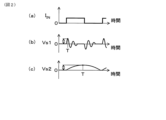
- FIG. 2(a) shows the case where the excitation current IIN supplied to the magnetosensitive body 11 is a pulse current.
- the MI sensor element 2 can be designed so that the response speed of the induced voltage varies with respect to changes in the rising edge of the pulse current.
- FIG. 2B shows the induced voltage Vs1 when the MI sensor element 2 is highly responsive when a magnetic field is acting on the MI sensor element 2 .
- FIG. 2(c) shows the induced voltage Vs2 when the MI sensor element 2 has a low response when a magnetic field acts on the MI sensor element 2.
- the induced voltage Vs1 when the MI sensor element 2 is highly responsive, the induced voltage Vs1 exhibits damped oscillation immediately after the pulse current rises. Then, at time T, the induced voltage Vs1 reaches its peak value. The peak value of the induced voltage Vs1 corresponds to the strength of the magnetic field acting on the MI sensor element 2.
- FIG. 2(b) When the MI sensor element 2 has a high response, the induced voltage Vs1 exhibits damped oscillation even immediately after the pulse current falls.
- the induced voltage Vs2 gently rises immediately after the pulse current rises. Then, at time T, the induced voltage Vs2 reaches its peak value.
- the peak value of the induced voltage Vs2 corresponds to the strength of the magnetic field acting on the MI sensor element 2.
- FIG. 2(c) the induced voltage Vs2 gradually decreases immediately after the pulse current falls.
- the MI sensor element 2 may have a high-response configuration or a low-response configuration.
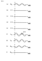
- the magnetic field B IN to be detected that acts on the magnetosensitive body 11 is assumed to change periodically in the direction of the magnetic field, and further, to change the strength of the magnetic field like a sine wave. I'll give you an example. However, the magnetic field B IN to be detected is exemplified for the sake of easy understanding of the explanation, and actually exhibits arbitrary behavior.
- the detection circuit 3 does not include the first feedback circuit 25 and the second feedback circuit 26, the potential difference across the detection coil 12 acts on the magnetosensitive body 11 as described with reference to FIG. It varies according to the strength of the target magnetic field B IN .
- the detection circuit 3 includes the first feedback circuit 25 and the second feedback circuit 26 as described above. Therefore, the feedback current IFB is generated so that the potential difference across the sensing coil 12 is zero.
- the detection coil 12 A return magnetic field BFB is generated. If the feedback magnetic field BFB can completely cancel the magnetic field BIN to be detected, the acting magnetic field BACT acting on the magnetosensitive body 11 becomes zero, as shown in FIG. 3(j).
- the acting magnetic field BACT acting on the magnetosensitive body 11 is almost zero. Therefore, even if the excitation current I IN is supplied to the magnetosensitive body 11 , the induced voltage of the detection coil 12 is almost zero because the applied magnetic field B ACT is almost zero. As shown in FIGS. 3(b) and 3(c), the voltages V1 and V2 across the detection coil 12 are substantially zero.
- the voltages V1 and V2 across the detection coil 12 are substantially zero, the voltages V3 and V4 at the inverting input terminal and the non-inverting input terminal of the main amplifier circuit 22 are also substantially zero, as shown in FIGS. becomes zero. Therefore, as shown in FIG. 3(f), the voltage V5 at the output terminal of the main amplifier circuit 22 also becomes substantially zero.
- the detection circuit 3 includes the first feedback circuit 25 and the second feedback circuit 26 to generate the feedback current IFB .
- the feedback current I FB is determined by the potential difference ⁇ Vx between the first feedback voltage V FB1 and the second feedback voltage V FB2 and the impedance in the circuit flowing through the detection coil 12 .
- the impedance in the circuit flowing through the detection coil 12 is a combination of the impedance of the first impedance circuit 25b and the impedance of the second impedance circuit 26b.
- the second feedback voltage VFB2 becomes a voltage whose polarity is inverted with respect to the first feedback voltage VFB1 when the predetermined reference voltage VB is used as a reference.
- the second feedback voltage VFB2 is a voltage obtained by inverting the first feedback voltage VFB1 with respect to the predetermined reference voltage VB.
- a potential difference ⁇ Vx between the first feedback voltage VFB1 and the second feedback voltage VFB2 is a value larger than a potential difference between the first feedback voltage VFB1 and the predetermined reference voltage VB.
- the potential difference ⁇ Vx between the first feedback voltage VFB1 and the second feedback voltage VFB2 is double the potential difference between the first feedback voltage VFB1 and the predetermined reference voltage VB . It is double the potential difference from the predetermined reference voltage VB.
- a large feedback current IFB can be generated.
- Being able to generate a large feedback current I FB means that the feedback magnetic field B FB can be increased. That is, it is possible to generate a return magnetic field BFB for canceling a large magnetic field to be detected BIN , so that a large magnetic field to be detected BIN can be detected.
- Magnetic detection device 100 of a comparative example The configuration of the magnetic detection device 100 of the comparative example will be described with reference to FIG.
- a magnetic detection device 100 includes an MI sensor element 2 and a detection circuit 103 .
- the MI sensor element 2 is the same as the MI sensor element 2 in Embodiment 1 described above.
- the detection circuit 103 includes an excitation circuit 121 , a main amplifier circuit 122 , an input circuit 123 and a feedback circuit 124 .
- the same reference numerals are given to the same configurations as those of the first embodiment.
- the excitation circuit 121 supplies an excitation current IIN to the magnetosensitive body 11 and outputs a switch timing signal Sg for holding the induced voltage of the detection coil 12 to the switch Sw1 of the input circuit 123 .
- the main amplifier circuit 122 is composed of a main operational amplifier OP_M. In the comparative example, the main operational amplifier OP_M is composed of a dual power supply operational amplifier.
- the input circuit 123 has the same configuration as the first input circuit 23 of the first embodiment.
- the feedback circuit 124 has substantially the same configuration as the first feedback circuit 25 of the first embodiment.
- the feedback circuit 124 includes a circuit 124a configured by a feedback operational amplifier OP_FB and an impedance circuit 124b.
- the feedback operational amplifier OP_FB is composed of a dual power supply operational amplifier.
- the magnetic detection device 100 of the comparative example will be described with reference to FIG. As shown in FIG. 5(a), it is assumed that the magnetic field BIN to be detected acting on the magnetosensitive body 11 changes periodically in the direction of the magnetic field, and that the strength of the magnetic field changes like a sine wave. I'll give you an example.
- the detection circuit 103 since the detection circuit 103 includes the feedback circuit 124, the voltages V11 and V12 across the detection coil 12 are substantially zero, as shown in FIGS. 5(b) and 5(c). Since the voltages V11 and V12 across the detection coil 12 are substantially zero, the voltage V13 at the input terminal of the main amplifier circuit 122 is also substantially zero, as shown in FIG. 5(d). Therefore, as shown in FIG. 5(e), the voltage V14 at the output terminal of the main amplifier circuit 122 also becomes substantially zero.
- a feedback current IFB is generated by the detection circuit 103 including the feedback circuit 124 .
- the feedback current I FB is determined by the potential difference ⁇ Vy between the feedback voltage V FB and the ground voltage, which is a predetermined reference voltage, and the impedance in the circuit flowing through the detection coil 12 .
- the impedance in the circuit flowing through the detection coil 12 is the impedance of the impedance circuit 124b.
- the feedback voltage V FB behaves as shown in FIG. 5(f).
- a feedback current IFB corresponding to the potential difference ⁇ Vy between the feedback voltage VFB and the ground voltage is generated in the detection coil 12, and a feedback magnetic field BFB is generated.
- the acting magnetic field BACT acting on the magnetosensitive body 11 becomes substantially zero.
- FIG. 6 Comparison between First Embodiment and Comparative Example Referring to FIG. 6, the magnetic detection device 1 of the first embodiment and the magnetic detection device 100 of the comparative example are compared.
- the relationship between the detection target magnetic field BIN and the potential difference ⁇ Vx between the first feedback voltage VFB1 and the second feedback voltage VFB2 is shown by a solid line.
- a potential difference ⁇ Vx between the first feedback voltage VFB1 and the second feedback voltage VFB2 corresponds to the feedback current IFB . Therefore, in Embodiment 1, the relationship between the magnetic field B IN to be detected and the feedback current I FB is also the same.
- the thick dashed line shows the relationship between the magnetic field B IN to be detected and the potential difference ⁇ Vy between the feedback voltage V FB and the ground voltage in the magnetic detection device 100 of the comparative example.
- the potential difference ⁇ Vy between the feedback voltage VFB and the ground voltage corresponds to the feedback current IFB . Therefore, in the comparative example, the relationship between the magnetic field B IN to be detected and the feedback current I FB is also the same. Since the second end 12b of the detection coil 12 is grounded, the potential difference ⁇ Vy between the feedback voltage VFB and the ground voltage matches the feedback voltage VFB .
- the relationship between the magnetic field B IN to be detected and the potential difference ⁇ Vx has linearity in the range of ⁇ Bx around zero of the magnetic field B IN to be detected. That is, within the range of ⁇ Bx, the potential difference ⁇ Vx increases as the magnetic field BIN to be detected increases, and the rate of increase is constant.
- the potential difference ⁇ Vx reaches the positive upper limit, so that a larger feedback current IFB cannot be generated. Therefore, even if the strength of the magnetic field in one direction in the detection target magnetic field BIN becomes larger than Bx_max, the potential difference ⁇ Vx remains at the positive upper limit value. Note that when the first feedback voltage VFB1 reaches its upper limit, the potential difference ⁇ Vx reaches its positive upper limit.
- the potential difference ⁇ Vx reaches the negative lower limit, so a larger feedback current IFB can be generated. Gone. Therefore, even if the strength of the magnetic field in the other direction in the detection target magnetic field B IN becomes larger than the absolute value of Bx_min, the potential difference ⁇ Vx remains at the negative lower limit value. When the second feedback voltage VFB2 reaches its upper limit, the potential difference ⁇ Vx reaches its negative lower limit.
- the relationship between the magnetic field B IN to be detected and the potential difference ⁇ Vy has linearity in the range of ⁇ By around zero of the magnetic field B IN to be detected. That is, within the range of ⁇ By, the potential difference ⁇ Vy increases as the magnetic field BIN to be detected increases, and the rate of increase is constant.
- the potential difference ⁇ Vy reaches the positive upper limit value, making it impossible to generate a larger feedback current IFB . Therefore, even if the strength of the magnetic field in one direction in the magnetic field B IN to be detected becomes larger than By_max, the potential difference ⁇ Vy remains at the positive upper limit value. Note that when the feedback voltage VFB reaches the positive upper limit, the potential difference ⁇ Vy reaches the positive upper limit.
- the potential difference ⁇ Vy reaches the negative lower limit, so that a larger feedback current IFB can be generated. Gone. Therefore, even if the strength of the magnetic field in the other direction in the detection target magnetic field BIN becomes larger than the absolute value of By_min, the potential difference ⁇ Vy remains at the negative lower limit value. Note that when the feedback voltage VFB reaches the negative lower limit, the potential difference ⁇ Vy reaches the negative lower limit.
- the detectable ranges ⁇ Bx and ⁇ By of the magnetic field BIN to be detected depend on the maximum value of the feedback current IFB .
- the maximum value of the feedback current IFB depends on the magnitude of the potential difference ⁇ Vx (shown in FIG. 3(g)) between the first feedback voltage VFB1 and the second feedback voltage VFB2 .
- the second feedback voltage VFB2 is a voltage whose polarity is inverted with respect to the first feedback voltage VFB1 when the predetermined reference voltage VB is used as a reference.
- the second feedback voltage VFB2 is a voltage obtained by inverting the first feedback voltage VFB1 with respect to the predetermined reference voltage VB. Therefore, the first feedback voltage VFB1 and the second feedback voltage VFB2 behave as shown in FIG. 3(g).
- the potential difference ⁇ Vx between the first feedback voltage VFB1 and the second feedback voltage VFB2 is twice the potential difference between the first feedback voltage VFB1 and the predetermined reference voltage VB.
- the maximum value of the feedback current IFB depends on the potential difference ⁇ Vy (shown in FIG. 5(f)) between the feedback voltage VFB and the ground voltage.
- the maximum values of the first feedback voltage VFB1 and the second feedback voltage VFB2 in the first embodiment and the maximum value of the feedback voltage VFB in the comparative example depend on the maximum voltage that can be applied by the power supply. Also, the feedback current IFB depends on the impedance in the circuit flowing through the detection coil 12 .
- the maximum feedback current IFB in the first embodiment is The value is twice the maximum value of the feedback current IFB in the comparative example. That is, the magnetic detection device 1 of the first embodiment doubles the detectable range of the detection target magnetic field B IN as compared with the magnetic detection device 100 of the comparative example, even if the power supply voltage and impedance are the same. can be done.
- the magnetic detection device 1 of the present embodiment includes a main operational amplifier OP_M connected to the detection coil 12 and feedback circuits 25 and 26 connecting the output terminal of the main operational amplifier OP_M and the detection coil 12 .
- a feedback current IFB is generated in the detection coil 12, and the detection coil 12 generates a feedback magnetic field for canceling the magnetic field BIN to be detected.
- Generate B FB If the feedback magnetic field BFB completely cancels out the magnetic field BIN to be detected, the feedback current IFB or the feedback voltage VFB will be in a state corresponding to the strength of the magnetic field BIN to be detected.
- the detection target magnetic field BIN can be detected with high accuracy by detecting the feedback current IFB or the physical quantity corresponding to the feedback current IFB . be able to.
- the magnetic field BFB offsets the magnetic field BIN to be detected
- the magnetic field does not act on the magnetosensitive body 11 . Therefore, the feedback current I FB corresponding to the magnetic field B IN to be detected does not depend on the electromagnetic characteristics of the magnetosensitive body 11 . Then, the relationship between the magnetic field BIN to be detected and the feedback current IFB becomes a relationship having linearity. Therefore, by detecting the feedback current IFB or the physical quantity corresponding to the feedback current IFB , the detection accuracy of the magnetic field BIN to be detected can be improved.
- both ends of the detection coil 12 of the MI sensor element 2 are connected to the inverting input terminal and the non-inverting input terminal of the main operational amplifier OP_M. Furthermore, the magnetic detection device 1 has two feedback circuits 25 and 26 . One of the two feedback circuits 25 and 26 is the first feedback circuit 25 connected between the output terminal of the main operational amplifier OP_M and the first end 12 a of the detection coil 12 . The other of the two feedback circuits 25 and 26 is a second feedback circuit 26 connected between the output terminal of the main operational amplifier OP_M and the second end 12 b of the detection coil 12 .
- the feedback current IFB generated in the detection coil 12 is divided into the first feedback voltage VFB1 generated by the first feedback circuit 25 and the second feedback voltage VFB1 generated by the second feedback circuit 26.
- a current corresponding to the potential difference ⁇ Vx with respect to VFB2 can be, for example, the potential difference ⁇ Vx between the first feedback voltage VFB1 and the second feedback voltage VFB2 .
- the second feedback voltage VFB2 is a voltage whose polarity is inverted with respect to the first feedback voltage VFB1 when the predetermined reference voltage VB is used as a reference.
- the second feedback voltage VFB2 is a voltage obtained by inverting the first feedback voltage VFB1 with respect to the predetermined reference voltage VB. Therefore, the potential difference ⁇ Vx between the first feedback voltage VFB1 and the second feedback voltage VFB2 can be increased. That is, the feedback current IFB can be increased.
- the resistance of the circuit through which the feedback current IFB flows is neither reduced nor the power supply voltage is increased.
- the feedback current flowing through the detection coil 12 is reduced without decreasing the resistance of the circuit through which the feedback current IFB flows and without increasing the power supply voltage. It is possible to provide the magnetic detection device 1 capable of increasing the current IFB .
- a magnetic detection device 1 of this embodiment will be described with reference to FIG.
- a magnetic detection device 1 of this embodiment includes an MI sensor element 2 and a detection circuit 4 .
- the detection circuit 4 additionally includes a common feedback input voltage generation circuit 29 in addition to the detection circuit 3 of the first embodiment.
- the common feedback input voltage generating circuit 29 is the same as the first embodiment.
- the detection circuit 4 includes a signal output section 27 and a reference power supply 28 like the detection circuit 3 of the first embodiment, but they are omitted in FIG. It should be noted that, of the reference numerals used in Embodiment 2, the same reference numerals as those used in the above-described embodiments represent the same components and the like as those in the above-described embodiments unless otherwise specified.
- a common feedback input voltage generation circuit 29 (hereinafter simply referred to as “generation circuit 29”) is connected to the output terminal of the main operational amplifier OP_M, and performs phase adjustment processing, differentiation processing, and integration processing on the output voltage of the main operational amplifier OP_M. At least one process is performed.
- Generation circuit 29 generates a common feedback input voltage for first feedback circuit 25 and second feedback circuit 26 . That is, the generating circuit 29 is connected to the inverting input terminal of the first feedback operational amplifier OP_FB1 that constitutes the first feedback circuit 25 and the non-inverting input terminal of the second feedback operational amplifier OP_FB2 that constitutes the second feedback circuit 26. be.
- the generating circuit 29 is composed of an operational amplifier OP_S.
- the generation circuit 29 is configured to include resistors R13 and R14 and capacitors C5 and C6 according to the intended function.
- the operational amplifier OP_S is composed of a single power supply operational amplifier.
- one generating circuit 29 is used compared to the case of providing separate generating circuits. can simplify the circuit configuration. Furthermore, this embodiment also has the same effects as those of the first embodiment.
- the generation circuit 29 is a circuit that performs differentiation processing and integration processing, the phase of the input/output signal is inverted by 180°.
- the non-inverting input terminal of the main operational amplifier OP_M should be connected to the first end 12 a of the detection coil 12 and the inverting input terminal should be connected to the second end 12 b of the detection coil 12 .
- each of the operational amplifiers OP_M, OP_FB1, OP_FB2, and OP_S is composed of a single power supply operational amplifier, but can also be composed of a dual power supply operational amplifier.
- the predetermined reference voltage VB may be close to the ground potential instead of the positive voltage.
- the first feedback circuit 25 and the second feedback circuit 26 are directly connected to the output terminal of the main amplifier circuit 22 .
- the connection may be made so that an AD conversion circuit and a DA conversion circuit are interposed. This makes it possible to perform digital signal processing.
Landscapes
- Physics & Mathematics (AREA)
- Condensed Matter Physics & Semiconductors (AREA)
- General Physics & Mathematics (AREA)
- Chemical & Material Sciences (AREA)
- Engineering & Computer Science (AREA)
- Nanotechnology (AREA)
- Measuring Magnetic Variables (AREA)
Abstract
Description
反転入力端子および非反転入力端子の一方が前記検出コイルの第一端に接続され、かつ、前記反転入力端子および前記非反転入力端子の他方が前記検出コイルの前記第一端とは反対側の第二端に接続されたメインオペアンプと、
前記メインオペアンプの出力端子と前記検出コイルの前記第一端との間に接続され、前記検出コイルに帰還電流を生じさせるための第一帰還電圧を生成する第一帰還回路と、
前記メインオペアンプの出力端子と前記検出コイルの前記第二端との間に接続され、前記検出コイルに前記帰還電流を生じさせるために、所定基準電圧を基準とした場合に前記第一帰還電圧に対して極性を反転させた第二帰還電圧を生成する第二帰還回路と、
を備える、磁気検出装置にある。
1.磁気検出装置1の構成
実施形態1における磁気検出装置1について、図1を参照して説明する。図1に示すように、本形態の磁気検出装置1は、マグネトインピーダンスセンサ素子2(以下において、「MIセンサ素子」という。)と、検出回路3とを備える。
次に、MIセンサ素子2の動作について図2を参照して説明する。ここでは、MIセンサ素子2は、図1に示す検出回路3に接続されていない場合とする。つまり、MIセンサ素子2単体としての動作を説明する。
次に、磁気検出装置1の動作について図3を参照して説明する。図3において、検出対象磁場BINが感磁体11に作用している場合に、検出回路3における各部位の電圧V1~V5、第一帰還電圧VFB1、第二帰還電圧VFB2、帰還電流IFB、帰還磁場BFB、作用磁場BACTの挙動について説明する。
比較例の磁気検出装置100の構成について図4を参照して説明する。磁気検出装置100は、MIセンサ素子2と、検出回路103とを備える。MIセンサ素子2は、上述した実施形態1におけるMIセンサ素子2と同一である。
図6を参照して、実施形態1の磁気検出装置1と比較例の磁気検出装置100とを比較する。図6には、実線により、実施形態1の磁気検出装置1において、検出対象磁場BINと、第一帰還電圧VFB1と第二帰還電圧VFB2との電位差ΔVxとの関係を示す。第一帰還電圧VFB1と第二帰還電圧VFB2との電位差ΔVxは、帰還電流IFBに対応する。従って、実施形態1において、検出対象磁場BINと帰還電流IFBとの関係も同様の関係となる。
本形態の磁気検出装置1は、検出コイル12に接続されるメインオペアンプOP_Mと、メインオペアンプOP_Mの出力端子と検出コイル12とを接続する帰還回路25,26とを備える。当該構成により、感磁体11に検出対象磁場BINが作用している状態において、検出コイル12には帰還電流IFBに生じ、検出コイル12が、検出対象磁場BINを相殺するための帰還磁場BFBを発生する。仮に、帰還磁場BFBが検出対象磁場BINを完全に相殺する状態になれば、帰還電流IFBまたは帰還電圧VFBが、検出対象磁場BINの強さに対応する状態となる。つまり、帰還磁場BFBが検出対象磁場BINを完全に相殺できれば、帰還電流IFB、または、帰還電流IFBに対応する物理量を検出することで、高精度に検出対象磁場BINを検出することができる。
本形態の磁気検出装置1について図7を参照して説明する。本形態の磁気検出装置1は、MIセンサ素子2と、検出回路4とを備える。検出回路4は、実施形態1の検出回路3に対して、共通帰還入力電圧生成回路29を追加で備える。
実施形態1,2において、各オペアンプOP_M、OP_FB1、OP_FB2、OP_Sは、単電源オペアンプにより構成したが、両電源オペアンプにより構成することも可能である。この場合、所定基準電圧VBが正電圧ではなく、接地電位付近とすることもできる。
Claims (10)
- 励磁電流が供給された際に磁場の強さに対応して磁化変化を生じる感磁体、および、前記感磁体に巻回され前記感磁体の前記磁化変化により生じる誘導電圧を出力する検出コイルを備えるマグネトインピーダンスセンサ素子と、
反転入力端子および非反転入力端子の一方が前記検出コイルの第一端に接続され、かつ、前記反転入力端子および前記非反転入力端子の他方が前記検出コイルの前記第一端とは反対側の第二端に接続されたメインオペアンプと、
前記メインオペアンプの出力端子と前記検出コイルの前記第一端との間に接続され、前記検出コイルに帰還電流を生じさせるための第一帰還電圧を生成する第一帰還回路と、
前記メインオペアンプの出力端子と前記検出コイルの前記第二端との間に接続され、前記検出コイルに前記帰還電流を生じさせるために、所定基準電圧を基準とした場合に前記第一帰還電圧に対して極性を反転させた第二帰還電圧を生成する第二帰還回路と、
を備える、磁気検出装置。 - 前記第一帰還回路は、入力端子が前記メインオペアンプの出力端子側に接続され、かつ、出力端子が前記検出コイルの前記第一端側に接続された第一帰還用オペアンプを備え、
前記第二帰還回路は、入力端子が前記メインオペアンプの出力端子側に接続され、かつ、出力端子が前記検出コイルの前記第二端側に接続された第二帰還用オペアンプを備え、
前記第一帰還電圧は、前記第一帰還用オペアンプの出力端子の電圧であり、
前記第二帰還電圧は、前記第二帰還用オペアンプの出力端子の電圧であり、
前記第一帰還用オペアンプにおいて前記メインオペアンプの出力端子側に接続される入力端子と、前記第二帰還用オペアンプにおいて前記メインオペアンプの出力端子側に接続される入力端子とにおいて、一方の入力端子が反転入力端子であり、他方の入力端子が非反転入力端子である、請求項1に記載の磁気検出装置。 - 前記第一帰還回路の増幅率と前記第二帰還回路の増幅率とは、同一に設定され、
前記第二帰還電圧は、前記所定基準電圧を基準とした場合に前記第一帰還電圧を反転した電圧とされる、請求項2に記載の磁気検出装置。 - 前記第一帰還回路は、
前記第一帰還用オペアンプと、
前記第一帰還用オペアンプの出力端子と前記検出コイルの前記第一端との間に接続され、前記検出コイルにより出力される前記誘導電圧が前記第一帰還用オペアンプ側へ移動することを抑制する第一インピーダンス回路と、
を備え、
前記第二帰還回路は、
前記第二帰還用オペアンプと、
前記第二帰還用オペアンプの出力端子と前記検出コイルの前記第二端との間に接続され、前記検出コイルにより出力される前記誘導電圧が前記第二帰還用オペアンプ側へ移動することを抑制する第二インピーダンス回路と、
を備える、請求項2または3に記載の磁気検出装置。 - 前記第一インピーダンス回路のインピーダンスと前記第二インピーダンス回路のインピーダンスは、同一に設定されている、請求項4に記載の磁気検出装置。
- さらに、前記メインオペアンプの出力端子に接続され、前記メインオペアンプの出力電圧に対して位相調整処理、微分処理および積分処理の少なくとも1つの処理を行い、前記第一帰還回路および前記第二帰還回路に対する共通帰還入力電圧を生成する共通帰還入力電圧生成回路を備える、請求項1~5のいずれか1項に記載の磁気検出装置。
- さらに、
前記検出コイルの前記第一端と前記メインオペアンプの前記反転入力端子との間に接続され、所定タイミング時における前記第一端の電圧をホールドし、ホールドした前記第一端の電圧を前記メインオペアンプの前記反転入力端子に入力する第一入力回路と、
前記検出コイルの前記第二端と前記メインオペアンプの前記非反転入力端子との間に接続され、前記所定タイミングと同一のタイミング時における前記第二端の電圧をホールドし、ホールドした前記第二端の電圧を前記メインオペアンプの前記非反転入力端子に入力する第二入力回路と、
を備える、請求項1~6のいずれか1項に記載の磁気検出装置。 - 前記所定基準電圧は、正電圧である、請求項1~7のいずれか1項に記載の磁気検出装置。
- さらに、前記第一帰還回路および前記第二帰還回路に前記所定基準電圧としての前記正電圧を印加する共通の基準電源を備える、請求項8に記載の磁気検出装置。
- さらに、前記第一帰還電圧と前記第二帰還電圧との電位差、または、前記帰還電流を、前記感磁体に作用する検出対象磁場の強さを表す検出信号として出力する信号出力部を備える、請求項1~9のいずれか1項に記載の磁気検出装置。
Priority Applications (3)
| Application Number | Priority Date | Filing Date | Title |
|---|---|---|---|
| EP22880732.7A EP4394419A4 (en) | 2021-10-15 | 2022-09-21 | MAGNETIC DETECTION DEVICE |
| CN202280062384.2A CN118043693A (zh) | 2021-10-15 | 2022-09-21 | 磁检测装置 |
| US18/695,536 US20240288514A1 (en) | 2021-10-15 | 2022-09-21 | Magnetic detection device |
Applications Claiming Priority (2)
| Application Number | Priority Date | Filing Date | Title |
|---|---|---|---|
| JP2021169590A JP2023059528A (ja) | 2021-10-15 | 2021-10-15 | 磁気検出装置 |
| JP2021-169590 | 2021-10-15 |
Publications (1)
| Publication Number | Publication Date |
|---|---|
| WO2023063036A1 true WO2023063036A1 (ja) | 2023-04-20 |
Family
ID=85987479
Family Applications (1)
| Application Number | Title | Priority Date | Filing Date |
|---|---|---|---|
| PCT/JP2022/035129 WO2023063036A1 (ja) | 2021-10-15 | 2022-09-21 | 磁気検出装置 |
Country Status (6)
| Country | Link |
|---|---|
| US (1) | US20240288514A1 (ja) |
| EP (1) | EP4394419A4 (ja) |
| JP (1) | JP2023059528A (ja) |
| CN (1) | CN118043693A (ja) |
| TW (1) | TW202321725A (ja) |
| WO (1) | WO2023063036A1 (ja) |
Citations (9)
| Publication number | Priority date | Publication date | Assignee | Title |
|---|---|---|---|---|
| US4290018A (en) * | 1979-08-22 | 1981-09-15 | Rockwell International Corporation | Magnetic field strength measuring apparatus with triangular waveform drive means |
| JP2002198582A (ja) * | 2000-12-25 | 2002-07-12 | Aichi Steel Works Ltd | 磁場検出装置 |
| JP2008292325A (ja) * | 2007-05-24 | 2008-12-04 | Sanyo Electric Co Ltd | 信号検出回路 |
| CN101738587A (zh) * | 2008-11-24 | 2010-06-16 | 于文杰 | 一种微磁传感器 |
| JP2014029323A (ja) * | 2012-06-29 | 2014-02-13 | Anritsu Sanki System Co Ltd | 磁界分布検出装置、心磁計、および金属検出装置 |
| US20150048820A1 (en) * | 2013-08-15 | 2015-02-19 | Texas Instruments Deutschland Gmbh | Fluxgate magnetic sensor readout apparatus |
| JP5924503B2 (ja) | 2014-01-31 | 2016-05-25 | 愛知製鋼株式会社 | 磁気検出器 |
| JP2019184240A (ja) * | 2018-04-02 | 2019-10-24 | 愛知製鋼株式会社 | 磁気検出器 |
| WO2022070842A1 (ja) * | 2020-09-30 | 2022-04-07 | 愛知製鋼株式会社 | マグネトインピーダンスセンサ素子 |
Family Cites Families (2)
| Publication number | Priority date | Publication date | Assignee | Title |
|---|---|---|---|---|
| JP2002318250A (ja) * | 2001-02-16 | 2002-10-31 | Fuji Electric Co Ltd | 電流検出装置およびこれを用いた過負荷電流保安装置 |
| JP6223674B2 (ja) * | 2012-11-01 | 2017-11-01 | 矢崎総業株式会社 | 磁気検出装置 |
-
2021
- 2021-10-15 JP JP2021169590A patent/JP2023059528A/ja active Pending
-
2022
- 2022-09-21 US US18/695,536 patent/US20240288514A1/en active Pending
- 2022-09-21 CN CN202280062384.2A patent/CN118043693A/zh active Pending
- 2022-09-21 EP EP22880732.7A patent/EP4394419A4/en active Pending
- 2022-09-21 WO PCT/JP2022/035129 patent/WO2023063036A1/ja active Application Filing
- 2022-09-30 TW TW111137175A patent/TW202321725A/zh unknown
Patent Citations (9)
| Publication number | Priority date | Publication date | Assignee | Title |
|---|---|---|---|---|
| US4290018A (en) * | 1979-08-22 | 1981-09-15 | Rockwell International Corporation | Magnetic field strength measuring apparatus with triangular waveform drive means |
| JP2002198582A (ja) * | 2000-12-25 | 2002-07-12 | Aichi Steel Works Ltd | 磁場検出装置 |
| JP2008292325A (ja) * | 2007-05-24 | 2008-12-04 | Sanyo Electric Co Ltd | 信号検出回路 |
| CN101738587A (zh) * | 2008-11-24 | 2010-06-16 | 于文杰 | 一种微磁传感器 |
| JP2014029323A (ja) * | 2012-06-29 | 2014-02-13 | Anritsu Sanki System Co Ltd | 磁界分布検出装置、心磁計、および金属検出装置 |
| US20150048820A1 (en) * | 2013-08-15 | 2015-02-19 | Texas Instruments Deutschland Gmbh | Fluxgate magnetic sensor readout apparatus |
| JP5924503B2 (ja) | 2014-01-31 | 2016-05-25 | 愛知製鋼株式会社 | 磁気検出器 |
| JP2019184240A (ja) * | 2018-04-02 | 2019-10-24 | 愛知製鋼株式会社 | 磁気検出器 |
| WO2022070842A1 (ja) * | 2020-09-30 | 2022-04-07 | 愛知製鋼株式会社 | マグネトインピーダンスセンサ素子 |
Non-Patent Citations (1)
| Title |
|---|
| See also references of EP4394419A4 |
Also Published As
| Publication number | Publication date |
|---|---|
| US20240288514A1 (en) | 2024-08-29 |
| EP4394419A1 (en) | 2024-07-03 |
| JP2023059528A (ja) | 2023-04-27 |
| EP4394419A4 (en) | 2024-07-03 |
| CN118043693A (zh) | 2024-05-14 |
| TW202321725A (zh) | 2023-06-01 |
Similar Documents
| Publication | Publication Date | Title |
|---|---|---|
| US9841442B2 (en) | Current detecting device | |
| EP2871485B1 (en) | Current detection device | |
| US20200355758A1 (en) | Magnetic sensor | |
| KR101352308B1 (ko) | 센서 회로 | |
| JP5069997B2 (ja) | 地磁気センサ装置 | |
| CN102072694B (zh) | 电涡流式距离传感器 | |
| JP2012225664A (ja) | 電流センサ及び電流検出方法 | |
| CN109932670B (zh) | 基于上电置位的闭环tmr磁场测量装置 | |
| WO2023063036A1 (ja) | 磁気検出装置 | |
| CN111948438B (zh) | 一种低成本电流传感器 | |
| JP2005055300A (ja) | 電流センサ | |
| CN108732414B (zh) | 电流传感器及断路器 | |
| JP4406567B2 (ja) | 発振器により給電されるセンサの出力電圧を整流するための回路装置 | |
| JP7119633B2 (ja) | 磁気センサ | |
| JP2019002767A (ja) | 電流センサ | |
| CN108732415B (zh) | 交流传感器及断路器 | |
| JP3809635B2 (ja) | コイルの銅抵抗補償回路 | |
| JP2012063205A (ja) | 磁気センサ | |
| JP5758229B2 (ja) | 磁界検出装置 | |
| WO2024018869A1 (ja) | 磁気検出器 | |
| JP7119695B2 (ja) | 磁気センサ | |
| JPH07244137A (ja) | 磁界センサ | |
| JP3784225B2 (ja) | 画像形成装置 | |
| JPH0493772A (ja) | 直流電流検出器 | |
| JP5839387B2 (ja) | 磁界検出装置 |
Legal Events
| Date | Code | Title | Description |
|---|---|---|---|
| 121 | Ep: the epo has been informed by wipo that ep was designated in this application |
Ref document number: 22880732 Country of ref document: EP Kind code of ref document: A1 |
|
| WWE | Wipo information: entry into national phase |
Ref document number: 202280062384.2 Country of ref document: CN |
|
| WWE | Wipo information: entry into national phase |
Ref document number: 2022880732 Country of ref document: EP Ref document number: 22880732.7 Country of ref document: EP |
|
| WWE | Wipo information: entry into national phase |
Ref document number: 18695536 Country of ref document: US |
|
| ENP | Entry into the national phase |
Ref document number: 2022880732 Country of ref document: EP Effective date: 20240325 |
|
| NENP | Non-entry into the national phase |
Ref country code: DE |