WO2023058353A1 - 発光装置、発光装置の製造方法、および測距装置 - Google Patents
発光装置、発光装置の製造方法、および測距装置 Download PDFInfo
- Publication number
- WO2023058353A1 WO2023058353A1 PCT/JP2022/031981 JP2022031981W WO2023058353A1 WO 2023058353 A1 WO2023058353 A1 WO 2023058353A1 JP 2022031981 W JP2022031981 W JP 2022031981W WO 2023058353 A1 WO2023058353 A1 WO 2023058353A1
- Authority
- WO
- WIPO (PCT)
- Prior art keywords
- light
- substrate
- groove
- light emitting
- emitting device
- Prior art date
- Legal status (The legal status is an assumption and is not a legal conclusion. Google has not performed a legal analysis and makes no representation as to the accuracy of the status listed.)
- Ceased
Links
Images










Classifications
-
- H—ELECTRICITY
- H01—ELECTRIC ELEMENTS
- H01S—DEVICES USING THE PROCESS OF LIGHT AMPLIFICATION BY STIMULATED EMISSION OF RADIATION [LASER] TO AMPLIFY OR GENERATE LIGHT; DEVICES USING STIMULATED EMISSION OF ELECTROMAGNETIC RADIATION IN WAVE RANGES OTHER THAN OPTICAL
- H01S5/00—Semiconductor lasers
- H01S5/02—Structural details or components not essential to laser action
- H01S5/022—Mountings; Housings
- H01S5/0225—Out-coupling of light
- H01S5/02253—Out-coupling of light using lenses
-
- G—PHYSICS
- G01—MEASURING; TESTING
- G01S—RADIO DIRECTION-FINDING; RADIO NAVIGATION; DETERMINING DISTANCE OR VELOCITY BY USE OF RADIO WAVES; LOCATING OR PRESENCE-DETECTING BY USE OF THE REFLECTION OR RERADIATION OF RADIO WAVES; ANALOGOUS ARRANGEMENTS USING OTHER WAVES
- G01S17/00—Systems using the reflection or reradiation of electromagnetic waves other than radio waves, e.g. lidar systems
- G01S17/02—Systems using the reflection of electromagnetic waves other than radio waves
- G01S17/06—Systems determining position data of a target
- G01S17/08—Systems determining position data of a target for measuring distance only
-
- G—PHYSICS
- G01—MEASURING; TESTING
- G01S—RADIO DIRECTION-FINDING; RADIO NAVIGATION; DETERMINING DISTANCE OR VELOCITY BY USE OF RADIO WAVES; LOCATING OR PRESENCE-DETECTING BY USE OF THE REFLECTION OR RERADIATION OF RADIO WAVES; ANALOGOUS ARRANGEMENTS USING OTHER WAVES
- G01S7/00—Details of systems according to groups G01S13/00, G01S15/00, G01S17/00
- G01S7/48—Details of systems according to groups G01S13/00, G01S15/00, G01S17/00 of systems according to group G01S17/00
- G01S7/481—Constructional features, e.g. arrangements of optical elements
-
- G—PHYSICS
- G01—MEASURING; TESTING
- G01S—RADIO DIRECTION-FINDING; RADIO NAVIGATION; DETERMINING DISTANCE OR VELOCITY BY USE OF RADIO WAVES; LOCATING OR PRESENCE-DETECTING BY USE OF THE REFLECTION OR RERADIATION OF RADIO WAVES; ANALOGOUS ARRANGEMENTS USING OTHER WAVES
- G01S7/00—Details of systems according to groups G01S13/00, G01S15/00, G01S17/00
- G01S7/48—Details of systems according to groups G01S13/00, G01S15/00, G01S17/00 of systems according to group G01S17/00
- G01S7/481—Constructional features, e.g. arrangements of optical elements
- G01S7/4814—Constructional features, e.g. arrangements of optical elements of transmitters alone
- G01S7/4815—Constructional features, e.g. arrangements of optical elements of transmitters alone using multiple transmitters
-
- G—PHYSICS
- G02—OPTICS
- G02B—OPTICAL ELEMENTS, SYSTEMS OR APPARATUS
- G02B3/00—Simple or compound lenses
-
- G—PHYSICS
- G02—OPTICS
- G02B—OPTICAL ELEMENTS, SYSTEMS OR APPARATUS
- G02B5/00—Optical elements other than lenses
-
- H—ELECTRICITY
- H01—ELECTRIC ELEMENTS
- H01S—DEVICES USING THE PROCESS OF LIGHT AMPLIFICATION BY STIMULATED EMISSION OF RADIATION [LASER] TO AMPLIFY OR GENERATE LIGHT; DEVICES USING STIMULATED EMISSION OF ELECTROMAGNETIC RADIATION IN WAVE RANGES OTHER THAN OPTICAL
- H01S5/00—Semiconductor lasers
- H01S5/02—Structural details or components not essential to laser action
- H01S5/022—Mountings; Housings
- H01S5/023—Mount members, e.g. sub-mount members
- H01S5/02325—Mechanically integrated components on mount members or optical micro-benches
- H01S5/02326—Arrangements for relative positioning of laser diodes and optical components, e.g. grooves in the mount to fix optical fibres or lenses
-
- H—ELECTRICITY
- H10—SEMICONDUCTOR DEVICES; ELECTRIC SOLID-STATE DEVICES NOT OTHERWISE PROVIDED FOR
- H10H—INORGANIC LIGHT-EMITTING SEMICONDUCTOR DEVICES HAVING POTENTIAL BARRIERS
- H10H20/00—Individual inorganic light-emitting semiconductor devices having potential barriers, e.g. light-emitting diodes [LED]
- H10H20/80—Constructional details
- H10H20/85—Packages
- H10H20/855—Optical field-shaping means, e.g. lenses
-
- H—ELECTRICITY
- H01—ELECTRIC ELEMENTS
- H01S—DEVICES USING THE PROCESS OF LIGHT AMPLIFICATION BY STIMULATED EMISSION OF RADIATION [LASER] TO AMPLIFY OR GENERATE LIGHT; DEVICES USING STIMULATED EMISSION OF ELECTROMAGNETIC RADIATION IN WAVE RANGES OTHER THAN OPTICAL
- H01S5/00—Semiconductor lasers
- H01S5/40—Arrangement of two or more semiconductor lasers, not provided for in groups H01S5/02 - H01S5/30
- H01S5/42—Arrays of surface emitting lasers
- H01S5/423—Arrays of surface emitting lasers having a vertical cavity
Definitions
- the present disclosure relates to a light-emitting device, a method for manufacturing the light-emitting device, and a rangefinder.
- VCSELs Vertical Cavity Surface Emitting Lasers
- a plurality of light-emitting elements are provided in a two-dimensional array on the front or rear surface of a substrate.
- crosstalk occurs when the light emitted from a certain light emitting element is not directed to the corresponding lens but directed to another lens. Such light is called stray light. It is desirable to suppress the generation of stray light.
- the present disclosure provides a light-emitting device, a method for manufacturing the light-emitting device, and a distance measuring device, which are capable of allowing the light emitted from the light-emitting element to be preferably incident on the lens.
- a light-emitting device includes a substrate, a plurality of light-emitting elements provided on a first surface side of the substrate, and a plurality of lenses provided on a second surface side of the substrate,
- the substrate includes a first groove having a shape surrounding a first lens included in the plurality of lenses, and the first groove includes a first side surface provided on the first lens side and the first lens. and an inclination angle of the first side surface with respect to the first surface or the second surface is 80 degrees or more and 100 degrees or less.
- the inclination angle of the second side surface with respect to the first surface or the second surface may be 80 degrees or more and 100 degrees or less.
- the light emitted from the light emitting element is totally reflected by the second side surface, and this light is preferably incident on the first lens, and the cross-sectional shape of the first groove is made line-symmetrical or line-symmetrical. It is possible to make a similar shape.
- the first groove may have a bottom surface between the first side surface and the second side surface.
- the first groove may have a bottom surface between the first side surface and the second side surface.
- the first side surface and the second side surface may be in contact with each other within the first groove.
- the first groove a V-shaped groove, it is possible to set the inclination angle of the first side surface to 80 degrees or more and 100 degrees or less.
- the first groove may penetrate the substrate. As a result, for example, it is possible to prevent light from passing through the gap between the first surface of the substrate and the groove surface of the first groove.
- the first groove may have a depth such that the light emitted from the light emitting element does not enter the deepest portion of the groove surface of the first groove. As a result, for example, it is possible to prevent light from passing through the gap between the first surface of the substrate and the groove surface of the first groove.
- the first groove may have a width equal to or greater than the wavelength of light emitted by the light emitting element. As a result, for example, it is possible to suppress the transmission of light through the first grooves.
- the first groove may have a shape such that light emitted from the light emitting element is totally reflected by the first side surface. As a result, for example, it is possible to prevent light from exiting the substrate from the first side surface.
- the light emitting device on the first side surface may further include an insulating film provided within the first groove. This makes it possible, for example, to protect the first groove with an insulating film and to adjust the refractive index in the first groove.
- the insulating film may have a refractive index of 2.3 or less. As a result, for example, the light incident on the first side surface can be totally reflected.
- the substrate further includes a second groove having a shape surrounding a second lens included in the plurality of lenses, and the second groove is provided on the second lens side. and a fourth side surface provided on the opposite side of the second lens, wherein the inclination angle of the third side surface with respect to the first surface or the second surface is 80 degrees or more and 100 degrees. It can be below. This makes it possible, for example, to cause the light emitted from the light emitting element to be totally reflected by the third side surface and to make this light preferably enter the second lens.
- the inclination angle of the fourth side surface with respect to the first surface or the second surface may be 80 degrees or more and 100 degrees or less.
- the light emitted from the light emitting element is totally reflected by the fourth side surface and is preferably incident on the second lens. It is possible to make a similar shape.
- the second groove may be separated from the first groove. This makes it possible, for example, to set these grooves to a simple shape.
- the second groove may be connected to the first groove. This makes it possible, for example, to save space for arranging these grooves.
- the plurality of lenses may be provided on the second surface of the substrate as part of the substrate. Thereby, for example, it becomes possible to easily form the lens by processing the substrate.
- a light-emitting device includes a substrate, a plurality of light-emitting elements provided on the first surface side of the substrate, and a plurality of lenses provided on the second surface side of the substrate,
- the substrate includes a groove provided between the lenses, and the groove has a depth such that the light emitted from the light emitting element does not enter the deepest portion of the groove surface of the groove.
- the light emitted from the light emitting element can be prevented from becoming stray light or return light, and the light can be preferably incident on the first lens.
- a method for manufacturing a light-emitting device includes: forming a plurality of light-emitting elements on a first surface side of a substrate; forming a plurality of lenses on a second surface side of the substrate; forming a first groove having a shape surrounding a first lens included in the plurality of lenses, the first groove having a first side surface provided on the first lens side and the first lens;
- the inclination angle of the first side surface with respect to the first surface or the second surface is set to 80 degrees or more and 100 degrees or less.
- the first groove may be formed in the substrate from the second surface side of the substrate. This makes it possible, for example, to form the first groove after bonding the substrate to the support substrate.
- the first groove may be formed in the substrate from the first surface side of the substrate. This makes it possible, for example, to form the first grooves before bonding the substrate to the support substrate.
- the method for manufacturing a light-emitting device may further include forming a light-shielding film on each of the lenses, covering a portion of the upper surface of each of the lenses.
- the performance of the lens can be adjusted by the light shielding film.
- a distance measuring device includes a plurality of light-emitting elements that generate light, a light-emitting section that irradiates a subject with light from the light-emitting elements, and a light-receiving section that receives light reflected from the subject. and a distance measuring unit for measuring a distance to the subject based on the light received by the light receiving unit, wherein the light emitting unit includes a substrate and the plurality of light emitting units provided on the first surface side of the substrate.
- the substrate includes a first groove having a shape surrounding a first lens included in the plurality of lenses, and
- the first groove has a first side surface provided on the side of the first lens and a second side surface provided on the side opposite to the first lens, and the first groove has the first side surface provided on the side of the first lens and the second side surface provided on the side opposite to the first lens.
- the inclination angle of one side surface is 80 degrees or more and 100 degrees or less.
- a distance measuring device includes a plurality of light-emitting elements that generate light, a light-emitting section that irradiates a subject with light from the light-emitting elements, and a light-receiving section that receives light reflected from the subject. and a distance measuring unit for measuring a distance to the subject based on the light received by the light receiving unit, wherein the light emitting unit includes a substrate and a plurality of light emitting units provided on the first surface side of the substrate.
- the light emitted from the light emitting element can be prevented from becoming stray light or return light, and the light can be preferably incident on the first lens.
- FIG. 1 is a block diagram showing a configuration example of a distance measuring device according to a first embodiment
- FIG. 3 is a diagram for explaining the STL (Structured Light) method of the first embodiment
- 1 is a cross-sectional view showing an example of the structure of a light emitting device according to a first embodiment
- FIG. 4 is a cross-sectional view showing the structure of the light emitting device shown in FIG. 3B
- FIG. 1A and 1B are a sectional view and a plan view showing the structure of a light emitting device according to a first embodiment
- FIG. 3 is a cross-sectional view showing the structure of a light-emitting device as a comparative example of the first embodiment
- 3A and 3B are a cross-sectional view and a plan view showing the structure of a light-emitting device according to a modification of the first embodiment
- FIG. FIG. 4 is a plan view showing the structure of a light emitting device of another modified example of the first embodiment
- FIG. 4 is a cross-sectional view showing the structure of a light-emitting device of another modified example of the first embodiment
- FIG. 4 is a cross-sectional view showing the structure of a light-emitting device of another modified example of the first embodiment
- FIG. 4 is a cross-sectional view showing the structure of a light-emitting device of another modified example of the first embodiment
- FIG. 4 is a cross-sectional view showing the structure of a light-emitting device of another modified example of the first embodiment; 2 is a cross-sectional view (1/2) showing the method for manufacturing the light emitting device of the first embodiment; FIG. 2 is a cross-sectional view (2/2) showing the method for manufacturing the light emitting device of the first embodiment; FIG. FIG. 4 is a cross-sectional view showing the structure of a light emitting device according to a second embodiment; FIG. 10 is a cross-sectional view showing the structure of a light emitting device as a comparative example of the second embodiment; It is a cross-sectional view showing the structure of a light-emitting device of a modification of the second embodiment.
- FIG. 11 is a cross-sectional view (3/6) showing the method for manufacturing the light emitting device of the second embodiment;
- FIG. 4A is a cross-sectional view (4/6) showing the method for manufacturing the light emitting device of the second embodiment;
- FIG. 11 is a cross-sectional view (5/6) showing the method for manufacturing the light emitting device of the second embodiment;
- 6 is a cross-sectional view (6/6) showing the method for manufacturing the light emitting device of the second embodiment;
- FIG. 11A is a cross-sectional view (1/4) showing a method of manufacturing a light emitting device according to a modification of the second embodiment; It is a cross-sectional view (2/4) showing the manufacturing method of the light emitting device of the modified example of the second embodiment.
- FIG. 11 is a cross-sectional view (3/4) showing a method of manufacturing a light emitting device according to a modification of the second embodiment;
- FIG. 11 is a cross-sectional view (4/4) showing a method of manufacturing a light emitting device according to a modification of the second embodiment; It is a sectional view showing a manufacturing method of a light-emitting device of another modification of a 2nd embodiment.
- FIG. 1 is a block diagram showing a configuration example of the range finder 101 of the first embodiment.
- the distance measuring device 101 includes a light emitting unit 102, a driving unit 103, a power supply circuit 104, a light emitting side optical system 105, a light receiving side optical system 106, a light receiving unit 107, a signal processing unit 108, a control unit 109, and a temperature detection unit.
- a section 110 is provided.
- the light emitting unit 102 emits light from a plurality of light sources.
- the light emitting unit 102 of this example has a light emitting element 102a by VCSEL (Vertical Cavity Surface Emitting LASER) as each light source, and the light emitting elements 102a are arranged in a predetermined manner such as a matrix. configured.
- VCSEL Vertical Cavity Surface Emitting LASER
- the drive unit 103 is configured with a power supply circuit for driving the light emitting unit 102 .
- the power supply circuit 104 generates a power supply voltage for the drive unit 103 based on an input voltage from a battery (not shown) provided in the distance measuring device 101, for example.
- the driving section 103 drives the light emitting section 102 based on the power supply voltage.
- the light emitted from the light emitting unit 102 is applied to the subject S as the distance measurement target through the light emitting side optical system 105 . Reflected light from the subject S of the light irradiated in this way enters the light receiving surface of the light receiving unit 107 via the light receiving side optical system 106 .
- the light receiving unit 107 is, for example, a light receiving element such as a CCD (Charge Coupled Device) sensor or a CMOS (Complementary Metal Oxide Semiconductor) sensor. It receives light, converts it to an electrical signal, and outputs it.
- a light receiving element such as a CCD (Charge Coupled Device) sensor or a CMOS (Complementary Metal Oxide Semiconductor) sensor. It receives light, converts it to an electrical signal, and outputs it.
- the light receiving unit 107 performs, for example, CDS (Correlated Double Sampling) processing, AGC (Automatic Gain Control) processing, etc. on an electrical signal obtained by photoelectrically converting the received light, and further performs A/D (Analog/Digital) conversion. process. Then, the signal as digital data is output to the signal processing unit 108 in the subsequent stage.
- CDS Correlated Double Sampling
- AGC Automatic Gain Control
- the light receiving unit 107 of this example outputs the frame synchronization signal Fs to the driving unit 103 . Accordingly, the drive unit 103 can cause the light emitting element 102a in the light emitting unit 102 to emit light at a timing corresponding to the frame cycle of the light receiving unit 107.
- FIG. 1
- the signal processing unit 108 is configured as a signal processing processor such as a DSP (Digital Signal Processor).
- the signal processing unit 108 performs various signal processing on the digital signal input from the light receiving unit 107 .
- the control unit 109 includes, for example, a microcomputer having a CPU (Central Processing Unit), a ROM (Read Only Memory), a RAM (Random Access Memory), or an information processing device such as a DSP. It controls the driving unit 103 for controlling the operation and controls the light receiving operation of the light receiving unit 107 .
- a microcomputer having a CPU (Central Processing Unit), a ROM (Read Only Memory), a RAM (Random Access Memory), or an information processing device such as a DSP. It controls the driving unit 103 for controlling the operation and controls the light receiving operation of the light receiving unit 107 .
- the control unit 109 has a function as a distance measuring unit 109a.
- the distance measuring unit 109a measures the distance to the subject S based on a signal input via the signal processing unit 108 (that is, a signal obtained by receiving reflected light from the subject S).
- the distance measurement unit 109a of this example measures the distance of each part of the subject S in order to specify the three-dimensional shape of the subject S.
- the temperature detection unit 110 detects the temperature of the light emitting unit 102 .
- the temperature detection unit 110 for example, a configuration that detects temperature using a diode can be adopted.
- the temperature information detected by the temperature detection unit 110 is supplied to the driving unit 103, which enables the driving unit 103 to drive the light emitting unit 102 based on the temperature information.
- (1.2) Ranging Method As a ranging method in the ranging device 101, for example, a ranging method based on the STL (Structured Light) method or the ToF (Time of Flight) method is adopted. be able to.
- STL Structured Light
- ToF Time of Flight
- the STL method is a method of measuring the distance based on an image of the subject S irradiated with light having a predetermined bright/dark pattern such as a dot pattern or grid pattern.
- FIG. 2 is a diagram for explaining the STL method of the first embodiment.
- the subject S is irradiated with pattern light Lp having a dot pattern as shown in A of FIG. 2, for example.
- the pattern light Lp is divided into a plurality of blocks BL, and each block BL is assigned a different dot pattern (a dot pattern is prevented from overlapping between blocks B).
- FIG. 2B is an explanatory diagram of the principle of distance measurement of the STL method.
- the wall W and the box BX placed in front of it are the subject S, and the subject S is irradiated with the pattern light Lp.
- “G” in the drawing schematically represents the angle of view of the light receiving unit 107 .
- BLn in the figure means the light of a certain block BL in the pattern light Lp
- dn means the dot pattern of the block BLn projected on the received light image by the light receiving unit 107.
- the dot pattern of the block BLn appears at the position of "dn'" in the received light image. That is, the position where the pattern of the block BLn appears in the received light image differs between when the box BX exists and when the box BX does not exist. Specifically, pattern distortion occurs.
- the STL method is a method that obtains the shape and depth of the subject S by utilizing the fact that the irradiated pattern is distorted by the object shape of the subject S. Specifically, this method obtains the shape and depth of the object S from the distortion of the pattern.
- the light receiving unit 107 for example, an IR (Infrared: infrared) light receiving unit using a global shutter method is used.
- the distance measuring unit 109a controls the driving unit 103 so that the light emitting unit 102 emits pattern light, and detects pattern distortion in the image signal obtained through the signal processing unit 108. , to calculate the distance based on how the pattern is distorted.
- the ToF method measures the distance to the object by detecting the flight time (time difference) of the light emitted from the light emitting unit 102 and reflected by the object until it reaches the light receiving unit 107. It is a method to
- the distance measuring unit 109a calculates the time difference between the light emitted by the light emitting unit 102 and the light received by the light receiving unit 107 from the time when the light is emitted from the light emitting unit 102 to the time when the light is received by the light receiving unit 107, based on the signal input via the signal processing unit 108. and the speed of light.
- a light receiving unit capable of receiving IR is used as the light receiving unit 107 .
- FIG. 3 is a cross-sectional view showing an example of the structure of the light emitting device 1 of the first embodiment.
- the light-emitting device 1 of this embodiment may be a part of the distance measuring device 101 or may be the distance measuring device 101 itself.
- FIG. 3A shows a first example of the structure of the light emitting device 1 of this embodiment.
- the light-emitting device 1 of this example includes an LD chip 41 including a light-emitting portion 102, an LDD substrate 42 including a driving portion 103, a mounting substrate 43, a heat dissipation substrate 44, a correction lens holding portion 45, and one or more correction A lens 46 and wiring 47 are provided.
- a in FIG. 3 shows the X-axis, Y-axis, and Z-axis that are perpendicular to each other.
- the X and Y directions correspond to the lateral direction (horizontal direction), and the Z direction corresponds to the longitudinal direction (vertical direction).
- the +Z direction corresponds to the upward direction, and the -Z direction corresponds to the downward direction.
- the -Z direction may or may not exactly match the direction of gravity.
- the LD chip 41 is arranged on the mounting board 43 via the heat dissipation board 44 , and the LDD board 42 is also arranged on the mounting board 43 .
- the mounting substrate 43 is, for example, a printed circuit board.
- the light receiving section 107 and the signal processing section 108 shown in FIG. 1 may be further arranged on the mounting board 43 .
- the heat dissipation substrate 44 is, for example, a ceramic substrate such as an aluminum oxide substrate or an aluminum nitride substrate.
- the correction lens holding part 45 is arranged on the heat dissipation substrate 44 so as to surround the LD chip 41 and holds one or more correction lenses 46 above the LD chip 41 .
- These correction lenses 46 are included in the light-emitting side optical system 105 described above. The light emitted from the light emitting section 102 in the LD chip 41 is corrected by these correcting lenses 46 and then irradiated onto the subject S described above.
- FIG. 3A shows, as an example, two correction lenses 46 held by the correction lens holding portion 45.
- the wiring 47 is provided on the front surface, back surface, inside, etc. of the mounting substrate 43 and electrically connects the LD chip 41 and the LDD substrate 42 .
- the wiring 47 is, for example, a printed wiring provided on the front surface or the rear surface of the mounting substrate 43 or a via wiring that penetrates the mounting substrate 43 .
- the wiring 47 of this embodiment also passes through or near the heat dissipation substrate 44 .
- FIG. 3B shows a second example of the structure of the light emitting device 1 of this embodiment.
- the light emitting device 1 of this example has the same components as the light emitting device 1 of the first example, but has bumps 48 instead of the wirings 47 .
- the LDD substrate 42 is arranged on the heat dissipation substrate 44, and the LD chip 41 is arranged on the LDD substrate 42.
- the LD chip 41 is placed on the LDD substrate 42 via the bumps 48 and electrically connected to the LDD substrate 42 by the bumps 48 .
- the light-emitting device 1 of this embodiment will be described below assuming that it has the structure of the second example shown in FIG. 3B. However, the following description is also applicable to the light emitting device 1 having the structure of the first example, except for the description of the structure specific to the second example.
- FIG. 4 is a cross-sectional view showing the structure of the light emitting device 1 shown in FIG. 3B.
- FIG. 4 shows a cross section of the LD chip 41 and the LDD substrate 42 in the light emitting device 1.
- the LD chip 41 includes a substrate 51, a laminated film 52, a plurality of light emitting elements 53, a plurality of anode electrodes 54, and a plurality of cathode electrodes 55.
- the LDD substrate 42 is , a substrate 61 and a plurality of connection pads 62 .
- a light-emitting element 53 shown in FIG. 4 is a specific example of the above-described light-emitting element 102a. 4, illustration of a lens 71 and a groove 72, which will be described later, is omitted (see FIG. 5).
- the substrate 51 is a semiconductor substrate such as a GaAs (gallium arsenide) substrate.
- FIG. 4 shows the front surface S1 of the substrate 51 facing the ⁇ Z direction and the rear surface S2 of the substrate 51 facing the +Z direction.
- the front surface S1 and back surface S2 shown in FIG. 4 are perpendicular to the Z direction.
- the front surface S1 is an example of the first surface of the present disclosure
- the back surface S2 is an example of the second surface of the present disclosure.
- the laminated film 52 includes multiple layers laminated on the surface S1 of the substrate 51 . Examples of these layers are an n-type semiconductor layer, an active layer, a p-type semiconductor layer, a light reflecting layer, an insulating layer with an exit window for light, and the like.
- the laminated film 52 includes a plurality of mesa portions M projecting in the -Z direction. A part of these mesa portions M are a plurality of light emitting elements 53 .
- the light emitting element 53 is provided on the surface S1 side of the substrate 51 as part of the laminated film 52 .
- the light emitting element 53 of this embodiment has a VCSEL structure and emits light in the +Z direction. As shown in FIG. 4, the light emitted from the light emitting element 53 passes through the substrate 51 from the front surface S1 to the rear surface S2, and enters the correcting lens 46 (FIG. 3) from the substrate 51.
- the LD chip 41 of this embodiment is a back emission type VCSEL chip.
- the anode electrode 54 is formed on the bottom surface of the light emitting element 53 .
- the cathode electrode 55 is formed on the lower surface of the mesa portion M other than the light emitting element 53 and extends to the lower surface of the laminated film 52 between the mesa portions M. As shown in FIG. Each light emitting element 53 emits light when a current flows between the corresponding anode electrode 54 and the corresponding cathode electrode 55 .
- the LD chip 41 is arranged on the LDD substrate 42 via the bumps 48 and electrically connected to the LDD substrate 42 by the bumps 48 .
- a connection pad 62 is formed on a substrate 61 included in the LDD substrate 42
- a mesa portion M is arranged on the connection pad 62 via a bump 48 .
- Each mesa portion M is arranged on the bump 48 via the anode electrode 54 or the cathode electrode 55 .
- the substrate 61 is, for example, a semiconductor substrate such as a Si (silicon) substrate.
- the LDD substrate 42 includes a driving section 103 that drives the light emitting section 102 .
- FIG. 4 schematically shows a plurality of switches SW included in the driving section 103. As shown in FIG. Each switch SW is electrically connected to the corresponding light emitting element 53 via the bump 48 .
- the driving unit 103 of this embodiment can control (turn on/off) these switches SW individually. Therefore, the drive unit 103 can drive the plurality of light emitting elements 53 individually. This makes it possible to precisely control the light emitted from the light emitting unit 102, for example, by causing only the light emitting element 53 required for distance measurement to emit light.
- Such individual control of the light emitting elements 53 can be realized by arranging the LDD substrate 42 below the LD chip 41, thereby making it easier to electrically connect each light emitting element 53 to the corresponding switch SW. ing.
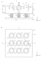
- FIG. 5 is a cross-sectional view and a plan view showing the structure of the light emitting device 1 of the first embodiment.
- FIG. 5A shows a cross section of the LD chip 41 and the LDD substrate 42 in the light emitting device 1.
- the LD chip 41 includes the substrate 51, the laminated film 52, the plurality of light emitting elements 53, the plurality of anode electrodes 54, and the plurality of cathode electrodes 55.
- the LDD substrate 42 is a substrate 61 and a plurality of connection pads 62 .
- illustration of the anode electrode 54, the cathode electrode 55, and the connection pad 62 is omitted.
- the LD chip 41 of this embodiment includes a plurality of light emitting elements 53 on the front surface S1 side of the substrate 51, and a plurality of lenses 71 and a plurality of grooves 72 on the rear surface S2 side of the substrate 51. It has 5B shows the layout of the lens 71 and the groove 72 provided on the back surface S2 side of the substrate 51.
- FIG. FIG. 5A shows a cross section along line A-A' shown in FIG. 5B.
- FIG. 5A Details of the lens 71 and the groove 72 of the present embodiment will be described below with reference to FIG. 5A. In this description, FIG. 5B will also be referred to as appropriate.
- the lenses 71 are arranged in a two-dimensional array similar to the light emitting elements 53 .
- the lenses 71 of this embodiment correspond to the light emitting elements 53 on a one-to-one basis, and each lens 71 is arranged in the +Z direction of one light emitting element 53 .
- the lenses 71 of this embodiment are arranged in a square grid pattern in FIG. 5B, they may be arranged in another layout.
- the lens 71 of the present embodiment is provided as a part of the substrate 51 on the rear surface S2 of the substrate 51, as shown in FIG. 5A.
- the lens 71 of this embodiment is a convex lens, and is formed as a part of the substrate 51 by etching the rear surface S2 of the substrate 51 into a convex shape.
- the lens 71 can be easily formed by etching the substrate 51 to form the lens 71 .
- the lens 71 of this embodiment may be a lens other than a convex lens, such as a concave lens, a binary lens, or a Fresnel lens.
- the grooves 72 are provided between the lenses 71 within the substrate 51 . As shown in FIG. 5B, the grooves 72 of this embodiment correspond to the lenses 71 one-to-one, and each groove 72 has a shape surrounding one lens 71 . Each groove 72 of this embodiment has an annular shape in plan view, and surrounds one lens 71 in an annular shape. Each groove 72 is filled with air (air gap) in this embodiment, but may also be filled with some solid material, for example an insulator such as quartz.
- each groove 72 will be described by taking the groove 72 surrounding the lens 71 indicated by L as an example.
- the lens 71 denoted by symbol L will be called "lens L".
- Lens L is an example of a first lens of this disclosure
- groove 72 surrounding lens L is an example of a first groove of this disclosure.
- the lens 71 other than the lens L is an example of the second lens of the present disclosure
- the groove 72 surrounding the lens 71 other than the lens L is an example of the second groove of the present disclosure.
- the following description also applies to the lens 71 other than the lens L and the groove 72 surrounding the lens 71 other than the lens L.
- the groove 72 surrounding the lens L has a side surface Sa on the side of the lens L, a side surface Sb opposite to the lens L, and a bottom surface Sc between the side surface Sa and the side surface Sb.
- the cross-sectional shape of the groove 72 is rectangular (rectangular groove) as shown in FIG. 5A, specifically rectangular. Therefore, the side surface Sa of this embodiment is parallel to the Z direction, and the inclination angle of the side surface Sa with respect to the front surface S1 and the rear surface S2 of the substrate 51 is 90 degrees. Similarly, the side surface Sb of this embodiment is parallel to the Z direction, and the inclination angle of the side surface Sb with respect to the front surface S1 and the rear surface S2 of the substrate 51 is 90 degrees.
- the bottom surface Sc of this embodiment is perpendicular to the Z direction. Side Sa is an example of the first side of the present disclosure, and side Sb is an example of the second side of the present disclosure.
- the inclination angle of the side surface Sa with respect to the front surface S1 and the rear surface S2 of the substrate 51 may be other than 90 degrees, for example, 80 degrees or more and 100 degrees or less.
- the inclination angle of the side surface Sb with respect to the front surface S1 and the rear surface S2 of the substrate 51 may be other than 90 degrees, and may be, for example, 80 degrees or more and 100 degrees or less.
- the cross-sectional shape of the side surface Sa, the side surface Sb, and the bottom surface Sc may be a curved line instead of a straight line.
- the groove 72 surrounding the lens L may have only the side surface Sa and the side surface Sb instead of having the side surface Sa, the side surface Sb and the bottom surface Sc. Examples of such grooves 72 will be described later.
- the substrate 51 of this embodiment has a plurality of grooves 72, and these grooves 72 are separated from each other within the substrate 51 as shown in FIG. 5B.
- groove 72 surrounding lens L is not connected to other grooves 72 in substrate 51 .
- these grooves 72 may be connected to each other within the substrate 51 . Examples of such grooves 72 will be described later.
- the light emitted from the plurality of light emitting elements 53 passes through the substrate 51 from the surface S1 to the rear surface S2 of the substrate 51 and enters the plurality of lenses 71 .
- the light emitted from each light emitting element 53 enters one corresponding lens 71 .
- the light emitted from the plurality of light emitting elements 53 can be shaped for each individual lens 71 .
- the light that has passed through the plurality of lenses 71 passes through the correction lens 46 (FIG. 3) and is irradiated onto the subject S (FIG. 1).
- the arrows indicate optical paths in which light emitted from one light emitting element 53 enters the corresponding lens 71 .
- the light emitted from the light emitting element 53 enters the side surface of the groove 72 , is reflected by the side surface of the groove 72 , and enters the lens 71 .
- This side surface is provided on the lens 71 side within the groove 72 in the same manner as the above-described side surface Sa.
- FIG. 5A further shows the minimum incident angle ⁇ of light incident on this side surface.
- This light is incident on the boundary between the side and bottom surfaces of the groove 72 .
- the groove 72 of this embodiment has a shape in which this minimum incident angle ⁇ is equal to or greater than the critical angle of total reflection on the side surface of the groove 72 . Therefore, the light incident on the side surface of the groove 72 of the present embodiment is totally reflected by the side surface of the groove 72 regardless of where the light is incident on the side surface of the groove 72 . This makes it possible to prevent the light from exiting the substrate 51 through the side surfaces of the grooves 72 .
- the inclination angle of the side surface of the groove 72 is 90 degrees, it is easy to set the minimum incident angle ⁇ to a large value and to set the minimum incident angle ⁇ to the critical angle or more. Therefore, according to this embodiment, it is possible to easily realize the groove 72 in which total reflection occurs. Thereby, it becomes possible to improve the utilization efficiency of light and suppress the generation of stray light. The reason why it is easy to set the minimum incident angle .theta.
- FIG. 5A shows the thickness T of the substrate 51, the width (diameter) w of the lens 71, the depth d of the groove 72, and the width t of the groove 72.
- the thickness T of the substrate 51 is, for example, 50-150 ⁇ m.
- the width w of the lens 71 is, for example, 10-30 ⁇ m.
- the width w of the lenses 71 may be the same for all the lenses 71 or may be different for each lens 71 .
- the width w of the lens 71 of this embodiment is set to about 20 ⁇ m.
- the radiation angle of the light emitting element 53 is the maximum tilt angle of the light emitted by the light emitting element 53 .
- the radiation angle of the light emitting element 53 is represented by ⁇
- the light emitted from the light emitting element 53 propagates in a direction inclined by a maximum angle ⁇ with respect to the +Z direction.
- this light is incident on the bottom surface Sc of the groove 72 while propagating from the light emitting element 53 to the corresponding lens L, the light is reflected by the bottom surface Sc of the groove 72 and becomes return light.
- the depth d of the groove 72 of the present embodiment sufficiently large so that the light emitted from the light emitting element 53 does not enter the bottom surface Sc of the groove 72 .
- This can be realized by setting the depth d of the groove 72 sufficiently large so that the light propagating in the direction inclined by the angle ⁇ with respect to the +Z direction does not enter the bottom surface Sc of the groove 72 .
- Such setting of the depth d of the groove 72 can also be applied when the cross-sectional shape of the groove 72 is a shape other than a rectangle. In this case, it is desirable to set the depth d of the groove 72 sufficiently large so that the light emitted from the light emitting element 53 does not enter the deepest portion of the groove surface of the groove 72 .
- the groove surface is a surface (for example, a side surface or a bottom surface) forming the groove 72 .
- the deepest portion is the deepest portion of the surface forming the groove 72 .
- the deepest portion of the groove surface of the groove 72 surrounding the lens L shown in FIG. 5A is the bottom surface Sc of the groove 72 .
- the cross-sectional shape of the groove 72 is V-shaped, the deepest part is the tip of the V-shape (see symbol V shown in A of FIG. 10).
- the width t of the groove 72 is desirable to set in consideration of the wavelength of the light emitted by the light emitting element 53, for example.
- the wavelength of the light emitted by the light emitting element 53 is represented by ⁇
- the width t of the groove 72 is preferably set to be two times or more the wavelength ⁇ , more preferably three times or more the wavelength ⁇ .
- the groove 72 of the present embodiment may be filled with air, as described above, or may be filled with an insulator.
- insulators are the aforementioned quartz and metal oxides such as Ta 2 O 5 , Nb 2 O 5 , TiO 2 (where Ta stands for tantalum, Nb for niobium and Ti for titanium). Quartz has a refractive index of 1.45, and such metal oxides have a refractive index of the order of 2.3. Since it is desirable that the insulator embedded in the trench 72 has a low refractive index, it is desirable to set the refractive index of the insulator to, for example, 2.3 or less. Burying such a metal oxide film in the trench 72 has the advantage of improving the light shielding property of the trench 72 and effectively suppressing the generation of stray light.
- the groove 72 of the present embodiment has a shape that totally reflects most of the light that is incident on the side surface of the groove 72 instead of having a shape that totally reflects all of the light that is incident on the side surface of the groove 72. may This makes it possible to obtain an effect similar to that obtained by total reflection of all light.
- the grooves 72 of the present embodiment may have a shape that causes all of the light incident on the side surfaces of the grooves 72 to be totally reflected or reflected to a degree close to total reflection. This makes it possible to obtain an effect similar to that obtained by total reflection of all light.
- the groove 72 of this embodiment has side surfaces parallel to the Z direction (vertical sidewalls), as described above.
- light is totally reflected by such side surfaces, so that reflected light with good symmetry can be obtained. Therefore, it is possible to preserve the fraction of light in the horizontal direction with respect to the optical axis parallel to the Z direction, and it is possible to preferably exhibit the collimation function of the lens 71 .
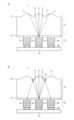
- FIG. 6 is a cross-sectional view showing the structure of a light-emitting device 1 as a comparative example of the first embodiment.
- FIG. 6A shows the structure of the light emitting device 1 of the first comparative example of the first embodiment.
- the light-emitting device 1 of this comparative example has a structure in which the groove 72 is removed from the light-emitting device 1 shown in FIG. 5A.
- the light emitted from the central light emitting element 53 is incident not only on the central lens 71 but also on the left and right lenses 71, causing crosstalk.
- stray light is generated in the light emitting device 1 of this comparative example. Since the stray light does not correctly contribute to the distance measurement by the distance measuring device 101, there is a possibility that the distance measurement performance is deteriorated.
- FIG. 6B shows the structure of the light emitting device 1 of the second comparative example of the first embodiment.
- the light-emitting device 1 of this comparative example has a structure in which the grooves 72 of the light-emitting device 1 shown in FIG. In FIG. 6B , part of the light emitted from the central light emitting element 53 is reflected by the light shielding film 73 and, as a result, does not enter the central lens 71 .
- return light is generated in the light emitting device 1 of this comparative example. Since the returned light does not contribute to the distance measurement by the distance measuring device 101, there is a possibility that the performance of the distance measurement is deteriorated.
- the light emitting device 1 of this embodiment has the grooves 72 as described above between the lenses 71 in the substrate 51 (A in FIG. 5). Therefore, according to the present embodiment, it is possible to suppress the generation of stray light and return light, and it is possible to make the light emitted from the light emitting element 53 preferably enter the lens 71 . For example, by totally reflecting the light emitted from the light emitting element 53 on the side surface of the groove 71, stray light can be suppressed. Further, by setting the depth d of the groove 72 to a value such that the light emitted from the light emitting element 53 does not enter the bottom surface Sc of the groove 72, it is possible to suppress return light.
- Light-emitting device 1 of a modified example of the first embodiment 7A and 7B are a cross-sectional view and a plan view showing the structure of a light-emitting device 1 according to a modification of the first embodiment.
- FIG. 7A shows a cross section of the light emitting device 1 of this modified example.
- the light emitting device 1 of this modification includes a plurality of lenses 71 and a plurality of grooves 72 annularly surrounding the lenses 71 .
- FIG. 7B shows the layout of these lenses 71 and grooves 72.
- FIG. 7A shows a cross section along line A-A' shown in FIG. 7B.
- these grooves 72 are connected to each other within the substrate 51 as shown in FIG. 7B. In other words, these grooves 72 form one large groove within substrate 51 . This makes it possible to save space for arranging these grooves 72 .
- the shape of the grooves 72 that are separated from each other is generally simpler than the shape of the grooves 72 that are connected to each other, it is better to separate the grooves 72 from each other if the shape of the grooves 72 is desired to be simple. desirable.
- FIG. 8 is a plan view showing the structure of the light emitting device 1 of another modified example of the first embodiment.
- lenses 71 are arranged in a square lattice.
- the square lattice shown in A of FIG. 5 and A of FIG. 7 is formed by a plurality of first straight lines parallel to the X direction and a plurality of second straight lines parallel to the Y direction.
- the square lattice shown in A of is formed by a plurality of first straight lines non-parallel to the X and Y directions and a plurality of second straight lines parallel to the X and Y directions.
- the first straight line extends in the +45 degree direction and the second straight line extends in the -45 degree direction.
- these lenses 71 may be arranged in any grid.
- lenses 71 are arranged irregularly.
- the light-emitting device 1 of this modification includes both grooves 72 that are connected to each other and grooves 72 that are separated from each other. Thus, these lenses 71 may be arranged regularly or irregularly.
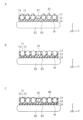
- FIG. 9 is a cross-sectional view showing the structure of the light-emitting device 1 of another modified example of the first embodiment.
- the groove 72 has a side surface Sa, a side surface Sb, and a bottom surface Sc.
- a symbol ⁇ shown in FIG. 9A indicates the inclination angle of the side surface Sa with respect to the front surface S1 and the rear surface S2 of the substrate 51 and the inclination angle of the side surface Sb with respect to the front surface S1 and the rear surface S2 of the substrate 51 .
- the inclination angle of the side surface Sa and the inclination angle of the side surface Sb are set to the same value.
- the inclination angle ⁇ of the side surfaces Sa and Sb of this modified example is set smaller than 90 degrees.
- the side faces Sa and Sb do not have to be parallel to the Z direction.
- the side surfaces Sa and Sb of the groove 72 of this modified example have a forward tapered shape, and the cross-sectional shape of the groove 72 is a trapezoid in which the upper base is longer than the lower base.
- the inclination angle ⁇ of the side surfaces Sa and Sb of this modified example is preferably set to 80 degrees or more for the reason described above.
- the groove 72 has a side surface Sa, a side surface Sb, and a bottom surface Sc.
- 9B also indicates the inclination angle of the side surface Sa with respect to the front surface S1 and the rear surface S2 of the substrate 51, and also indicates the inclination angle of the side surface Sb with respect to the front surface S1 and the rear surface S2 of the substrate 51.
- the inclination angle of the side surface Sa and the inclination angle of the side surface Sb are set to the same value.
- the inclination angle ⁇ of the side surfaces Sa and Sb of this modified example is set to be greater than 90 degrees.
- the side faces Sa and Sb do not have to be parallel to the Z direction.
- the side surfaces Sa and Sb of the groove 72 of this modified example have a reverse tapered shape, and the cross-sectional shape of the groove 72 is a trapezoid in which the upper base is shorter than the lower base.
- the inclination angle ⁇ of the side surfaces Sa and Sb of this modified example is preferably set to 100 degrees or less for the reason described above.
- the inclination angle ⁇ shown in FIGS. 9A and 9B is smaller than 90 degrees when the side surfaces Sa and Sb of the groove 72 have a forward tapered shape, and when the side surfaces Sa and Sb of the groove 72 have a reverse tapered shape. is specified to be greater than 90 degrees. Therefore, the inclination angle ⁇ shown in A of FIG. 9 is smaller than 90 degrees, and the inclination angle ⁇ shown in B of FIG. 9 is larger than 90 degrees.
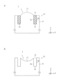
- FIG. 10 is a cross-sectional view showing the structure of the light emitting device 1 of another modified example of the first embodiment.
- the groove 72 has side surfaces Sa and side surfaces Sb, but does not have a bottom surface Sc.
- the cross-sectional shape of the groove 72 of this modified example is V-shaped (V-shaped groove), and the side surface Sa and the side surface Sb of the groove 72 are in contact with each other within the groove 72 .
- a of FIG. 10 shows a boundary line V between the side surface Sa and the side surface Sb.
- the boundary line V is located at the tip of the V shape and is the deepest part of the groove surface of the groove 72 .
- the inclination angle ⁇ of the side surfaces Sa and Sb of this modified example is preferably set to 80 degrees or more and less than 90 degrees.
- the groove 72 has a side surface Sa, a side surface Sb, and a bottom surface Sc.
- the cross-sectional shape of the bottom surface Sc in this modified example is not a straight line but a curved line, specifically, a downwardly convex curved line.
- the bottom end of the bottom surface Sc is the deepest part of the groove surface of the groove 72 .
- the inclination angle ⁇ of the side surfaces Sa and Sb of this modified example is also preferably set to 80 degrees or more and less than 90 degrees.
- the inclination angle ⁇ of the side surfaces Sa and Sb may be set to 90 degrees or more and 100 degrees or less.
- FIG. 11 is a cross-sectional view showing the structure of the light emitting device 1 of another modified example of the first embodiment.
- the light emitting device 1 further includes an insulating film 74 provided within the trench 72 .
- the insulating film 74 is, for example, a quartz film, or a metal oxide film such as a Ta 2 O 5 film, a Nb 2 O 5 film, or a TiO 2 film.
- the insulating film 74 of this modification covers the side surface Sa, the side surface Sb, and the bottom surface Sc of the trench 72 and fills the entire trench 72 .
- the insulating film 74 preferably has a refractive index of 2.3 or less.
- the lens 71 is not a convex lens but a concave lens.
- the lens 71 is formed as a part of the substrate 51 by etching the back surface S2 of the substrate 51 into a concave shape. According to this modification, the lens 71 can be easily formed by etching the substrate 51 to form the lens 71, as in the case where the lens 71 is a convex lens.
- each groove 72 is symmetrical with respect to the Z-axis.
- the cross-sectional shape of each groove 72 does not have to be line-symmetrical with respect to the Z-axis.
- the inclination angle of the side surface Sb may be different from the inclination angle of the side surface Sa. The same applies to the cross-sectional shape of each lens 71 .
- each lens 71 in plan view is point symmetrical with respect to the Z axis.
- the shape of each lens 71 in plan view does not have to be symmetrical with respect to the Z axis.
- the shape of each lens 71 in plan view may be elliptical instead of circular. The same applies to the shape of each groove 72 in plan view.
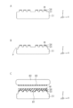
- FIGS. 12 and 13 are cross-sectional views showing a method for manufacturing the light-emitting device 1 of the first embodiment.
- the laminated film 52 and the light emitting element 53 are formed on the surface S1 of the substrate 51 (A in FIG. 12).
- a groove 72 is formed in the rear surface S2 of the substrate 51 (B in FIG. 12).
- the process of A of FIG. 12 is performed with the surface S1 of the substrate 51 facing upward.
- the step of B in FIG. 12 is performed with the rear surface S2 of the substrate 51 facing upward.
- the grooves 72 of this embodiment are formed by lithography and RIE (Reactive Ion Etching), for example. Each groove 72 is formed around the area where the corresponding lens 71 is to be formed. Further, each groove 72 is formed to have the side surface Sa, side surface Sb, and bottom surface Sc described with reference to FIGS. 5A and 5B.
- a lens 71 is formed on the rear surface S2 of the substrate 51 (A in FIG. 13).
- the lens 71 of this embodiment is formed by lithography and RIE, for example.
- Each lens 71 is formed inside a corresponding groove 72 .
- a structure in which each lens 71 is surrounded by a corresponding groove 72 is realized.
- the light emitting device 1 shown in FIGS. 5A and 5B is manufactured.
- the process of B in FIG. 13 is performed when manufacturing the light emitting device 1 shown in A in FIG.
- an insulating film 74 is formed on the entire rear surface S2 of the substrate 51, and then the insulating film 74 outside the grooves 72 is removed by etching. As a result, the trench 72 is filled with the insulating film 74 .
- the light-emitting device 1 shown in FIG. 11A is manufactured.
- step A in FIG. 12, the step B in FIG. 12, and the step A in FIG. 13 may be changed.
- these steps may be performed in the order of A in FIG. 12, A in FIG. 13, and B in FIG. That is, groove 72 may be formed after lens 71 is formed.
- the method shown in FIGS. 12A to 13A may be used to manufacture the light-emitting device 1 of each modification of the present embodiment.
- a concave lens is formed in the process of FIG. 13A.
- a V-shaped groove is formed in the process of FIG. 12B.
- the light emitting device 1 of this embodiment includes the grooves 72 having the shape described above.
- the groove 72 of this embodiment has a side surface Sa having an inclination angle of 80 degrees or more and 100 degrees or less.
- the depth d of the groove 72 in this embodiment is set to a value such that the light emitted from the light emitting element 53 does not enter the deepest portion of the groove surface of the groove 72 . Therefore, according to the present embodiment, the light emitted from the light emitting element 53 can be preferably incident on the lens 71 .
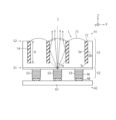
- FIG. 14 is a cross-sectional view showing the structure of the light emitting device 1 of the second embodiment.
- the light-emitting device 1 of this embodiment includes the same components as the light-emitting device 1 of the first embodiment (see A in FIG. 5, etc.).
- the groove 72 of this embodiment is a through groove penetrating the substrate 51 .
- the bottom surface Sc of the groove 72 is formed by the upper surface of the laminated film 52 .
- the depth d of the groove 72 in this embodiment is set to a value such that the light emitted from the light emitting element 53 does not enter the bottom surface Sc of the groove 72 . This makes it possible to effectively suppress the generation of stray light and return light.
- the groove 72 of the present embodiment may penetrate not only the substrate 51 but also a portion of the laminated film 52 other than the mesa portion M.
- the groove 72 of this embodiment penetrates the substrate 51 between the front surface S1 and the rear surface S2 of the substrate 51 .
- the groove 72 of the present embodiment may be formed by etching the substrate 51 from the front surface S1 side of the substrate 51, or may be formed by etching the substrate 51 from the rear surface S2 side of the substrate 51.
- the light-emitting device 1 of this embodiment further includes an insulating film 74 provided in the trench 72, similar to the light-emitting device 1 shown in FIG. 11A.
- the insulating film 74 is desirably made of, for example, a material with a low refractive index.
- the insulating film 74 may be formed of a material having a low coefficient of thermal expansion and a low modulus of elasticity. This makes it possible to suppress warping and cracking of the substrate 51 .
- FIG. 15 is a cross-sectional view showing the structure of a light-emitting device 1 as a comparative example of the second embodiment.
- the light emitting device 1 of this comparative example has the same components as the light emitting device 1 of the second embodiment (see FIG. 14). However, the groove 72 of this comparative example does not penetrate the substrate 51, and the depth d of the groove 72 of this comparative example is set shallow. Therefore, in this comparative example, stray light and return light may occur. On the other hand, according to this embodiment, it is possible to effectively suppress the generation of stray light and return light.
- FIG. 16 is a cross-sectional view showing the structure of the light-emitting device 1 of the modified example of the second embodiment.
- the light-emitting device 1 of this modification includes the same components as the light-emitting device 1 (see FIG. 15) of the comparative example of the second embodiment, and the groove 72 of this modification penetrates the substrate 51. do not have. However, the depth d of the groove 72 in this modified example is set deep.
- FIG. 16 shows the radiation angle ⁇ of the light emitting element 53.
- the radiation angle ⁇ of the light emitting element 53 is the maximum inclination angle of the light emitted by the light emitting element 53, as described above. Therefore, the light emitted from the light emitting element 53 propagates in a direction inclined by a maximum angle ⁇ with respect to the +Z direction.
- this light is incident on the bottom surface of the groove 72 while propagating from the light emitting element 53 to the corresponding lens 71, it is reflected by the bottom surface of the groove 72 and becomes return light.
- this light is incident on the side surface of the groove 72 while propagating from the light emitting element 53 to the corresponding lens 71, generation of return light can be suppressed.
- the depth d of the groove 72 in this modification sufficiently deep so that the light emitted from the light emitting element 53 does not enter the bottom surface of the groove 72 .
- This can be realized by setting the depth d of the groove 72 sufficiently deep so that the light propagating in the direction inclined by the angle ⁇ with respect to the +Z direction does not enter the bottom surface of the groove 72 .
- the depth d of the groove 72 in this modified example is set deep as described above. Specifically, the depth d of the groove 72 in this modified example is set to a value such that the light emitted from the light emitting element 53 does not enter the bottom surface of the groove 72, as shown in FIG. This makes it possible to effectively suppress the generation of stray light and return light.
- the light emitting device 1 of this embodiment may be manufactured by the method shown in FIGS. 12 and 13, or may be manufactured by the method described later.
- FIGS. 17 to 22 are cross-sectional views showing a method for manufacturing the light-emitting device 1 of the second embodiment.
- a laminated film 52, a plurality of light emitting elements 53, a plurality of anode electrodes 54, a plurality of cathode electrodes 55, etc. are formed on the upper surface of a substrate (wafer) 51 (A in FIG. 17).
- a substrate (wafer) 51 A in FIG. 17
- illustration of the laminated film 52 and the cathode electrode 55 is omitted.
- FIG. 17A also shows the plurality of mesas M described above.
- a light emitting element 53 and an anode electrode 54 are formed on the upper surface of a substrate 51 in this order. Note that the upper surface of the substrate 51 in A of FIG. 17 is the surface S1 of the substrate 51 .
- the edge portion of the substrate 51 is trimmed (B in FIG. 17).
- B of FIG. 17 shows the trimming point P of the substrate 51 .
- the lateral width of the trimming portion P is, for example, 1 to 5 mm. This trimming process is performed to suppress chipping and cracking of the substrate 51 when the thickness of the substrate 51 is reduced.
- an adhesive 81 is applied to the upper surface of the substrate 51 so as to cover the mesa portion M and the like (C in FIG. 17).
- the adhesive 81 may be an organic material or an inorganic material.
- the adhesive 81 is used to temporarily bond the substrate 51 and the support substrate 82 in this embodiment, but may be used to permanently bond the substrate 51 and the support substrate 82 together.
- a step of peeling the support substrate 82 from the substrate 51 is performed later.
- a step of scraping off the support substrate 82 from the substrate 51 is performed later.
- a release layer 83 is applied to the support substrate 82 (C in FIG. 17), and the substrate 51 and the support substrate 82 are bonded via the adhesive 81 and the release layer 83 (A in FIG. 18).
- the release layer 83 is decomposed with UV light (ultraviolet light), so that the step of peeling off the support substrate 82 from the substrate 51 is performed later.
- the release layer 83 may be thermally decomposed instead of being decomposed by UV light.
- the adhesive 81 contains the release layer 83
- the support substrate 82 does not have to be coated with the release layer 83.
- the substrate 51 and the support substrate 82 of this embodiment are bonded by one or more baking treatments at a bonding temperature of 80.degree. C. and a curing temperature of 120 to 190.degree.
- the substrate 51 of this embodiment is a GaAs substrate as described above.
- the support substrate 82 may be made of any material, but is preferably made of a material having a coefficient of thermal expansion close to that of GaAs so as not to warp after bonding to the substrate 51.
- deponding is performed using UV light, so it is desirable that the support substrate 82 be a glass substrate that transmits UV light.
- the support substrate 82 of this embodiment is, for example, a glass substrate having a transmittance of 80% or more for laser light having a wavelength of 355 nm and a coefficient of thermal expansion of about 5 to 6 ppm/°C.
- the thickness of the substrate 51 is reduced (B in FIG. 18).
- the substrate 51 is thinned by, for example, CMP (Chemical Mechanical Polishing). Note that the upper surface of the substrate 51 in FIG. 18B is the back surface S2 of the substrate 51 .
- a resist film 84 is formed on the substrate 51, and the resist film 84 is patterned (C in FIG. 18).
- a groove 72 is formed in the substrate 51 by dry etching using the resist film 84 as a mask (A in FIG. 19). The groove 72 is formed so as to penetrate the substrate 51 in this embodiment, but may be formed so as not to penetrate the substrate 51 .
- an insulating film 74 is formed on the substrate 51 (B in FIG. 19), and the insulating film 74 outside the trench 72 is removed by etching or CMP (C in FIG. 19). As a result, the trench 72 is filled with the insulating film 74 .
- the insulating film 74 is, for example, a silicon oxide film, an aluminum oxide film, an organic film, or the like.
- the insulating film 74 is desirably made of a material having a low refractive index, thermal expansion coefficient, and elastic modulus. It is desirable that the thickness of the insulating film 74 is, for example, 100 nm or more.
- the insulating film 74 can be formed by, for example, CVD (Chemical Vapor Deposition), sputtering, MBE (Molecular Beam Epitaxy), vapor deposition, spin coating, or the like.
- a resist film 85 is formed on the substrate 51, the resist film 85 is patterned, and the patterned resist film 85 is reflowed by heat treatment (A in FIG. 20). As a result, the resist film 85 is processed into a shape similar to the lens 71 .
- a lens 71 is formed on the upper surface of the substrate 51 by dry etching using the resist film 85 as a mask (B in FIG. 20).
- the lens 71 is formed as a part of the substrate 51 by processing the upper surface of the substrate 51 .
- an antireflection film (AR film) 86 is formed on the substrate 51 (C in FIG. 20). As a result, the upper surfaces of the lens 71 and the insulating film 74 are covered with the antireflection film 86 . If the antireflection film 86 is unnecessary, the process of C in FIG. 20 may be omitted.
- the dicing tape of the mounting device 87 is adhered to the substrate 51 (A in FIG. 21), and then the substrate 51 is turned upside down (B in FIG. 21). As a result, the substrate 51 is mounted on the dicing tape of the mounting device 87 and fixed to the dicing frame of the mounting device 87 .
- UV laser light is used to debond the support substrate 82 from the substrate 51 (B in FIG. 21).
- UV laser light transmitted through the support substrate 82 is irradiated onto the release layer 83 .
- the release layer 83 is decomposed (ablated) by UV laser light, and the support substrate 82 is peeled off from the substrate 51 .
- the adhesive 81 and the release layer 83 are removed by cleaning (C in FIG. 21).
- a laser device 88 for stealth dicing is used to irradiate the dicing line area in the substrate 51 with laser light (A in FIG. 22), and as a result, the substrate 51 is cut along the dicing line.
- the LD chip 41 shown in FIG. 14 is manufactured.
- This LD chip 41 is then placed on the LDD substrate 42 via a plurality of bumps 48 .
- the light emitting device 1 shown in FIG. 14 is manufactured.
- FIGS. 23 to 26 are cross-sectional views showing a method for manufacturing the light emitting device 1 of the modified example of the second embodiment. 17 to 22 and the methods shown in FIGS. 23 to 26 will be omitted as appropriate.
- a laminated film 52, a plurality of light emitting elements 53, a plurality of anode electrodes 54, a plurality of cathode electrodes 55, etc. are formed on the upper surface of a substrate (wafer) 51 (A in FIG. 23). However, illustration of the laminated film 52 and the cathode electrode 55 is omitted.
- FIG. 23A further shows the plurality of mesas M described above.
- a resist film 91 is formed on the substrate 51, and the resist film 91 is patterned (B in FIG. 23).
- a groove 72 is formed in the substrate 51 by dry etching using the resist film 91 as a mask (C in FIG. 23).
- the groove 72 of this modified example is formed so as to penetrate the substrate 51 by thinning the substrate 51, which will be described later.
- an insulating film 74 is formed on the substrate 51 (A in FIG. 24), and a resist film 92 is formed on the insulating film 74 (B in FIG. 24).
- the resist film 92 is patterned (B in FIG. 24), and a portion of the insulating film 74 outside the trench 72 is removed by dry etching using the resist film 92 as a mask (C in FIG. 24).
- the insulating film 74 is removed from the upper surfaces of the anode electrode 54 and the cathode electrode 55 (not shown). As a result, the trench 72 is filled with the insulating film 74 .
- FIG. 25A to 26C which will be described later, omit the illustration of the insulating film 74 remaining outside the trench 72 for the sake of clarity.
- FIG. 25A shows the same state as shown in FIG. 25C, but illustration of the insulating film 74 remaining outside the trench 72 is omitted.
- the edge portion of the substrate 51 is trimmed (B in FIG. 25).
- B of FIG. 25 shows the trimming point P of the substrate 51 .
- an adhesive 81 is applied to the upper surface of the substrate 51 so as to cover the mesa portion M and the like (C in FIG. 25).
- a release layer 83 is applied to the support substrate 82 (C in FIG. 25), and the substrate 51 and the support substrate 82 are bonded via the adhesive 81 and the release layer 83 (A in FIG. 26).
- the thickness of the substrate 51 is reduced (B in FIG. 26). As a result, groove 72 penetrates substrate 51 .
- a resist film 85 is formed on the substrate 51, the resist film 85 is patterned, and the patterned resist film 85 is reflowed by heat treatment (C in FIG. 26). As a result, the resist film 85 is processed into a shape similar to the lens 71 .
- the steps shown from B in FIG. 20 to C in FIG. 22 are performed.
- the LD chip 41 shown in FIG. 14 is manufactured.
- This LD chip 41 is then placed on the LDD substrate 42 via a plurality of bumps 48 .
- the light emitting device 1 shown in FIG. 14 is manufactured.
- the step of forming the trench 72 and the insulating film 74 instead of performing the step shown in FIG. It may be performed before performing the indicated steps. That is, the groove 72 and the insulating film 74 may be formed before forming the light emitting element 53 instead of forming after forming the light emitting element 53 .
- FIG. 27 is a cross-sectional view showing a method for manufacturing the light emitting device 1 of another modified example of the second embodiment.
- FIG. 27A shows the same state as shown in FIG. 19C.
- the side surface of the groove 72 shown in A of FIG. 27 has a forward tapered shape.
- the groove 72 may be formed so that the side surface thereof has a forward tapered shape.
- FIG. 27B shows the same state as shown in FIG. 20C.
- the lens 71 shown in FIG. 27B is partially covered with a light shielding film 93 instead of being entirely covered with the antireflection film 86 .
- the light shielding film 93 partially covers the upper surface of each lens 71 and forms an aperture of each lens 71 .
- light directed toward each lens 71 enters each lens 71 through this aperture.
- the light shielding film 93 is formed of, for example, a metal film having a light shielding property. In this manner, the lens 71 may be partially covered with the light shielding film 93 on its upper surface.
- the light emitting device 1 of this embodiment includes the grooves 72 having the shape described above.
- the groove 72 of this embodiment has a side surface Sa having an inclination angle of 80 degrees or more and 100 degrees or less, like the groove 72 of the first embodiment.
- the depth d of the groove 72 of the present embodiment is a value such that the light emitted from the light emitting element 53 does not enter the deepest portion of the groove surface of the groove 72, similarly to the depth d of the groove 72 of the first embodiment. is set to Therefore, according to the present embodiment, the light emitted from the light emitting element 53 can be preferably incident on the lens 71 .
- the light emitting device 1 of the first and second embodiments is used as the light source of the distance measuring device 101, it may be used in another mode.
- the light emitting device 1 of these embodiments may be used as a light source for optical equipment such as a printer, or may be used as a lighting device.
- a substrate (1) a substrate; a plurality of light emitting elements provided on the first surface side of the substrate; A plurality of lenses provided on the second surface side of the substrate, the substrate includes a first groove having a shape surrounding a first lens included in the plurality of lenses; The first groove has a first side surface provided on the first lens side and a second side surface provided on the opposite side of the first lens, The light-emitting device, wherein an inclination angle of the first side surface with respect to the first surface or the second surface is 80 degrees or more and 100 degrees or less.
- the substrate further includes a second groove having a shape surrounding a second lens included in the plurality of lenses;
- the second groove has a third side surface provided on the second lens side and a fourth side surface provided on the opposite side of the second lens,
- an inclination angle of the third side surface with respect to the first surface or the second surface is 80 degrees or more and 100 degrees or less.
- a substrate a plurality of light emitting elements provided on the first surface side of the substrate; A plurality of lenses provided on the second surface side of the substrate, the substrate includes grooves provided between the lenses; The light-emitting device, wherein the groove has a depth such that light emitted from the light-emitting element does not enter the deepest portion of the groove surface of the groove.
- a light-emitting unit that includes a plurality of light-emitting elements that generate light and irradiates a subject with light from the light-emitting elements; a light receiving unit that receives light reflected from the subject; a distance measuring unit that measures the distance to the subject based on the light received by the light receiving unit;
- the light emitting unit a substrate; the plurality of light emitting elements provided on the first surface side of the substrate; A plurality of lenses provided on the second surface side of the substrate, the substrate includes a first groove having a shape surrounding a first lens included in the plurality of lenses;
- the first groove has a first side surface provided on the first lens side and a second side surface provided on the opposite side of the first lens,
- a distance measuring device wherein an inclination angle of the first side surface with respect to the first surface or the second surface is 80 degrees or more and 100 degrees or less.
- a light-emitting unit that includes a plurality of light-emitting elements that generate light and irradiates a subject with light from the light-emitting elements; a light receiving unit that receives light reflected from the subject; a distance measuring unit that measures the distance to the subject based on the light received by the light receiving unit;
- the light emitting unit a substrate; a plurality of light emitting elements provided on the first surface side of the substrate; A plurality of lenses provided on the second surface side of the substrate, the substrate includes grooves provided between the lenses; The distance measuring device, wherein the groove has a depth such that the light emitted from the light emitting element does not enter the deepest portion of the groove surface of the groove.
Landscapes
- Physics & Mathematics (AREA)
- General Physics & Mathematics (AREA)
- Engineering & Computer Science (AREA)
- Electromagnetism (AREA)
- Optics & Photonics (AREA)
- Computer Networks & Wireless Communication (AREA)
- Radar, Positioning & Navigation (AREA)
- Remote Sensing (AREA)
- Condensed Matter Physics & Semiconductors (AREA)
- Optical Radar Systems And Details Thereof (AREA)
Priority Applications (3)
| Application Number | Priority Date | Filing Date | Title |
|---|---|---|---|
| CN202280066546.XA CN118044079A (zh) | 2021-10-07 | 2022-08-25 | 发光装置、发光装置的制造方法和距离测量装置 |
| JP2023552737A JPWO2023058353A1 (https=) | 2021-10-07 | 2022-08-25 | |
| US18/695,413 US20240396294A1 (en) | 2021-10-07 | 2022-08-25 | Light emitting device, method for manufacturing light emitting device, and distance measuring device |
Applications Claiming Priority (2)
| Application Number | Priority Date | Filing Date | Title |
|---|---|---|---|
| JP2021-165608 | 2021-10-07 | ||
| JP2021165608 | 2021-10-07 |
Publications (1)
| Publication Number | Publication Date |
|---|---|
| WO2023058353A1 true WO2023058353A1 (ja) | 2023-04-13 |
Family
ID=85803369
Family Applications (1)
| Application Number | Title | Priority Date | Filing Date |
|---|---|---|---|
| PCT/JP2022/031981 Ceased WO2023058353A1 (ja) | 2021-10-07 | 2022-08-25 | 発光装置、発光装置の製造方法、および測距装置 |
Country Status (4)
| Country | Link |
|---|---|
| US (1) | US20240396294A1 (https=) |
| JP (1) | JPWO2023058353A1 (https=) |
| CN (1) | CN118044079A (https=) |
| WO (1) | WO2023058353A1 (https=) |
Cited By (1)
| Publication number | Priority date | Publication date | Assignee | Title |
|---|---|---|---|---|
| WO2025033091A1 (ja) * | 2023-08-07 | 2025-02-13 | ソニーセミコンダクタソリューションズ株式会社 | 発光素子および測距装置 |
Families Citing this family (1)
| Publication number | Priority date | Publication date | Assignee | Title |
|---|---|---|---|---|
| JP2023037044A (ja) * | 2020-02-19 | 2023-03-15 | ソニーセミコンダクタソリューションズ株式会社 | 発光装置およびその製造方法 |
Citations (10)
| Publication number | Priority date | Publication date | Assignee | Title |
|---|---|---|---|---|
| JPS5849903A (ja) * | 1981-09-21 | 1983-03-24 | Canon Inc | マイクロレンズの遮光装置 |
| JP2001221975A (ja) * | 2000-02-10 | 2001-08-17 | Fujitsu Ltd | 光学装置 |
| JP2004220015A (ja) * | 2002-12-26 | 2004-08-05 | Sanyo Electric Co Ltd | 照明装置及び投写型映像表示装置 |
| JP2005037884A (ja) * | 2003-07-01 | 2005-02-10 | Nippon Sheet Glass Co Ltd | レンズプレートおよびその製造方法並びに画像伝達装置 |
| JP2012240352A (ja) * | 2011-05-23 | 2012-12-10 | Sony Corp | レンズ用金型及びウェーハレベルレンズ |
| JP2017116633A (ja) * | 2015-12-22 | 2017-06-29 | 大日本印刷株式会社 | レンズシート、撮像モジュール、撮像装置 |
| JP2019165198A (ja) * | 2018-03-19 | 2019-09-26 | 株式会社リコー | 面発光レーザアレイ、検出装置およびレーザ装置 |
| CN111353479A (zh) * | 2020-04-26 | 2020-06-30 | 欧菲微电子技术有限公司 | 微透镜组件、制备方法、光学指纹模组及电子装置 |
| WO2021024508A1 (ja) * | 2019-08-08 | 2021-02-11 | 富士ゼロックス株式会社 | 発光装置、光学装置及び情報処理装置 |
| WO2021149374A1 (ja) * | 2020-01-20 | 2021-07-29 | ソニーセミコンダクタソリューションズ株式会社 | 発光装置およびその製造方法 |
-
2022
- 2022-08-25 CN CN202280066546.XA patent/CN118044079A/zh not_active Withdrawn
- 2022-08-25 JP JP2023552737A patent/JPWO2023058353A1/ja active Pending
- 2022-08-25 WO PCT/JP2022/031981 patent/WO2023058353A1/ja not_active Ceased
- 2022-08-25 US US18/695,413 patent/US20240396294A1/en active Pending
Patent Citations (10)
| Publication number | Priority date | Publication date | Assignee | Title |
|---|---|---|---|---|
| JPS5849903A (ja) * | 1981-09-21 | 1983-03-24 | Canon Inc | マイクロレンズの遮光装置 |
| JP2001221975A (ja) * | 2000-02-10 | 2001-08-17 | Fujitsu Ltd | 光学装置 |
| JP2004220015A (ja) * | 2002-12-26 | 2004-08-05 | Sanyo Electric Co Ltd | 照明装置及び投写型映像表示装置 |
| JP2005037884A (ja) * | 2003-07-01 | 2005-02-10 | Nippon Sheet Glass Co Ltd | レンズプレートおよびその製造方法並びに画像伝達装置 |
| JP2012240352A (ja) * | 2011-05-23 | 2012-12-10 | Sony Corp | レンズ用金型及びウェーハレベルレンズ |
| JP2017116633A (ja) * | 2015-12-22 | 2017-06-29 | 大日本印刷株式会社 | レンズシート、撮像モジュール、撮像装置 |
| JP2019165198A (ja) * | 2018-03-19 | 2019-09-26 | 株式会社リコー | 面発光レーザアレイ、検出装置およびレーザ装置 |
| WO2021024508A1 (ja) * | 2019-08-08 | 2021-02-11 | 富士ゼロックス株式会社 | 発光装置、光学装置及び情報処理装置 |
| WO2021149374A1 (ja) * | 2020-01-20 | 2021-07-29 | ソニーセミコンダクタソリューションズ株式会社 | 発光装置およびその製造方法 |
| CN111353479A (zh) * | 2020-04-26 | 2020-06-30 | 欧菲微电子技术有限公司 | 微透镜组件、制备方法、光学指纹模组及电子装置 |
Cited By (1)
| Publication number | Priority date | Publication date | Assignee | Title |
|---|---|---|---|---|
| WO2025033091A1 (ja) * | 2023-08-07 | 2025-02-13 | ソニーセミコンダクタソリューションズ株式会社 | 発光素子および測距装置 |
Also Published As
| Publication number | Publication date |
|---|---|
| US20240396294A1 (en) | 2024-11-28 |
| CN118044079A (zh) | 2024-05-14 |
| JPWO2023058353A1 (https=) | 2023-04-13 |
Similar Documents
| Publication | Publication Date | Title |
|---|---|---|
| KR102160549B1 (ko) | 실리콘 제어 백플레인 상에 통합된 수직 이미터 | |
| JP6454576B2 (ja) | 光送信モジュール | |
| JPH08330679A (ja) | 光検出器一体型表面光レーザとこれを用いた光ピックアップ装置 | |
| JP2017112169A (ja) | イメージセンサ、撮像システム及びイメージセンサの製造方法 | |
| WO2023058353A1 (ja) | 発光装置、発光装置の製造方法、および測距装置 | |
| JP7547390B2 (ja) | 発光装置およびその製造方法 | |
| JP2014216588A (ja) | 発光装置、その製造方法、画像表示装置、及び画像形成装置 | |
| JP2006060204A (ja) | 自己監視式発光装置 | |
| WO2021149373A1 (ja) | 発光装置およびその製造方法 | |
| WO2021149372A1 (ja) | 発光装置およびその製造方法 | |
| CN111863983A (zh) | 生产带金属光学分离栅的光电发射和/或接收装置的方法 | |
| CN112802912B (zh) | 包括雪崩二极管阵列的集成电路及其制造方法 | |
| CN109655806A (zh) | 传感器设备 | |
| KR101359133B1 (ko) | 레이저 어셈블리, 이것의 형성 방법 및 이것을 포함하는장치 | |
| US20230030731A1 (en) | Light source device, method for manufacturing light source device, and electronic device | |
| JP4729893B2 (ja) | 半導体光学装置の製造方法 | |
| US20250132540A1 (en) | Light-emitting device, method for manufacturing light-emitting device, and distance measurement device | |
| JP6405368B2 (ja) | 光学式センサ | |
| US20230067340A1 (en) | Light emitting device and method of manufacturing the same | |
| JP5192847B2 (ja) | 発光装置 | |
| US20250038473A1 (en) | Light emitting device and distance measuring device | |
| US20240413077A1 (en) | Semiconductor device and distance measuring device | |
| WO2024024369A1 (ja) | 発光装置およびその製造方法 | |
| KR100985362B1 (ko) | 일체형 광모듈 패키지 및 그 제조방법 | |
| US20260121373A1 (en) | Light emitting device and method for manufacturing the same |
Legal Events
| Date | Code | Title | Description |
|---|---|---|---|
| 121 | Ep: the epo has been informed by wipo that ep was designated in this application |
Ref document number: 22878224 Country of ref document: EP Kind code of ref document: A1 |
|
| WWE | Wipo information: entry into national phase |
Ref document number: 2023552737 Country of ref document: JP |
|
| WWE | Wipo information: entry into national phase |
Ref document number: 18695413 Country of ref document: US |
|
| WWE | Wipo information: entry into national phase |
Ref document number: 202280066546.X Country of ref document: CN |
|
| NENP | Non-entry into the national phase |
Ref country code: DE |
|
| 122 | Ep: pct application non-entry in european phase |
Ref document number: 22878224 Country of ref document: EP Kind code of ref document: A1 |