WO2023054381A1 - Composition de résine photosensible, procédé de production de dispositif électronique, dispositif électronique et dispositif lumineux - Google Patents
Composition de résine photosensible, procédé de production de dispositif électronique, dispositif électronique et dispositif lumineux Download PDFInfo
- Publication number
- WO2023054381A1 WO2023054381A1 PCT/JP2022/035981 JP2022035981W WO2023054381A1 WO 2023054381 A1 WO2023054381 A1 WO 2023054381A1 JP 2022035981 W JP2022035981 W JP 2022035981W WO 2023054381 A1 WO2023054381 A1 WO 2023054381A1
- Authority
- WO
- WIPO (PCT)
- Prior art keywords
- photosensitive resin
- resin composition
- mass
- composition according
- meth
- Prior art date
Links
- 239000011342 resin composition Substances 0.000 title claims abstract description 141
- 238000004519 manufacturing process Methods 0.000 title claims description 25
- 229920001721 polyimide Polymers 0.000 claims abstract description 109
- 239000009719 polyimide resin Substances 0.000 claims abstract description 96
- -1 acrylate compound Chemical class 0.000 claims abstract description 59
- 238000006116 polymerization reaction Methods 0.000 claims abstract description 26
- 125000000962 organic group Chemical group 0.000 claims abstract description 24
- 239000003112 inhibitor Substances 0.000 claims abstract description 18
- 239000003795 chemical substances by application Substances 0.000 claims abstract description 16
- 239000011347 resin Substances 0.000 claims description 120
- 229920005989 resin Polymers 0.000 claims description 120
- 239000000758 substrate Substances 0.000 claims description 71
- 238000000034 method Methods 0.000 claims description 62
- 238000010438 heat treatment Methods 0.000 claims description 49
- 150000001875 compounds Chemical class 0.000 claims description 29
- 239000006087 Silane Coupling Agent Substances 0.000 claims description 26
- 239000003431 cross linking reagent Substances 0.000 claims description 22
- 125000001153 fluoro group Chemical group F* 0.000 claims description 14
- 125000003647 acryloyl group Chemical group O=C([*])C([H])=C([H])[H] 0.000 claims description 12
- 230000003287 optical effect Effects 0.000 claims description 12
- 229910052731 fluorine Inorganic materials 0.000 claims description 11
- 125000005462 imide group Chemical group 0.000 claims description 8
- 150000002989 phenols Chemical class 0.000 claims description 7
- 239000003504 photosensitizing agent Substances 0.000 claims description 6
- 229920001187 thermosetting polymer Polymers 0.000 claims description 6
- 239000004593 Epoxy Substances 0.000 claims description 5
- 125000003368 amide group Chemical group 0.000 claims description 4
- 230000001235 sensitizing effect Effects 0.000 abstract 1
- 239000010410 layer Substances 0.000 description 168
- 239000004065 semiconductor Substances 0.000 description 59
- 230000008569 process Effects 0.000 description 30
- 239000003960 organic solvent Substances 0.000 description 23
- 238000011161 development Methods 0.000 description 21
- 239000000126 substance Substances 0.000 description 21
- 239000004094 surface-active agent Substances 0.000 description 19
- 238000006243 chemical reaction Methods 0.000 description 17
- 239000000203 mixture Substances 0.000 description 17
- 239000007787 solid Substances 0.000 description 17
- 239000002966 varnish Substances 0.000 description 17
- KFZMGEQAYNKOFK-UHFFFAOYSA-N Isopropanol Chemical compound CC(C)O KFZMGEQAYNKOFK-UHFFFAOYSA-N 0.000 description 16
- 239000002253 acid Substances 0.000 description 16
- 239000000047 product Substances 0.000 description 16
- NIXOWILDQLNWCW-UHFFFAOYSA-M Acrylate Chemical compound [O-]C(=O)C=C NIXOWILDQLNWCW-UHFFFAOYSA-M 0.000 description 15
- 239000004642 Polyimide Substances 0.000 description 13
- 229910000679 solder Inorganic materials 0.000 description 13
- 239000000243 solution Substances 0.000 description 13
- 125000000524 functional group Chemical group 0.000 description 12
- 125000004018 acid anhydride group Chemical group 0.000 description 11
- 239000003054 catalyst Substances 0.000 description 11
- 238000012545 processing Methods 0.000 description 11
- 150000003254 radicals Chemical class 0.000 description 11
- 235000012431 wafers Nutrition 0.000 description 11
- 230000015572 biosynthetic process Effects 0.000 description 10
- 239000010949 copper Substances 0.000 description 10
- BGTOWKSIORTVQH-UHFFFAOYSA-N cyclopentanone Chemical compound O=C1CCCC1 BGTOWKSIORTVQH-UHFFFAOYSA-N 0.000 description 10
- 239000002904 solvent Substances 0.000 description 10
- XLYOFNOQVPJJNP-UHFFFAOYSA-N water Substances O XLYOFNOQVPJJNP-UHFFFAOYSA-N 0.000 description 10
- OKKJLVBELUTLKV-UHFFFAOYSA-N Methanol Chemical compound OC OKKJLVBELUTLKV-UHFFFAOYSA-N 0.000 description 9
- GTDPSWPPOUPBNX-UHFFFAOYSA-N ac1mqpva Chemical compound CC12C(=O)OC(=O)C1(C)C1(C)C2(C)C(=O)OC1=O GTDPSWPPOUPBNX-UHFFFAOYSA-N 0.000 description 9
- 239000012298 atmosphere Substances 0.000 description 9
- 229940042596 viscoat Drugs 0.000 description 9
- NVKGJHAQGWCWDI-UHFFFAOYSA-N 4-[4-amino-2-(trifluoromethyl)phenyl]-3-(trifluoromethyl)aniline Chemical group FC(F)(F)C1=CC(N)=CC=C1C1=CC=C(N)C=C1C(F)(F)F NVKGJHAQGWCWDI-UHFFFAOYSA-N 0.000 description 8
- XUIMIQQOPSSXEZ-UHFFFAOYSA-N Silicon Chemical group [Si] XUIMIQQOPSSXEZ-UHFFFAOYSA-N 0.000 description 8
- 150000001252 acrylic acid derivatives Chemical class 0.000 description 8
- 125000002947 alkylene group Chemical group 0.000 description 8
- 238000001035 drying Methods 0.000 description 8
- LZCLXQDLBQLTDK-UHFFFAOYSA-N ethyl 2-hydroxypropanoate Chemical compound CCOC(=O)C(C)O LZCLXQDLBQLTDK-UHFFFAOYSA-N 0.000 description 8
- 229910052710 silicon Inorganic materials 0.000 description 8
- 125000003700 epoxy group Chemical group 0.000 description 7
- 230000006872 improvement Effects 0.000 description 7
- 229910052751 metal Inorganic materials 0.000 description 7
- LLHKCFNBLRBOGN-UHFFFAOYSA-N propylene glycol methyl ether acetate Chemical compound COCC(C)OC(C)=O LLHKCFNBLRBOGN-UHFFFAOYSA-N 0.000 description 7
- 239000002994 raw material Substances 0.000 description 7
- 238000003756 stirring Methods 0.000 description 7
- YEJRWHAVMIAJKC-UHFFFAOYSA-N 4-Butyrolactone Chemical compound O=C1CCCO1 YEJRWHAVMIAJKC-UHFFFAOYSA-N 0.000 description 6
- 125000000217 alkyl group Chemical group 0.000 description 6
- 150000004985 diamines Chemical class 0.000 description 6
- 230000006870 function Effects 0.000 description 6
- 238000005227 gel permeation chromatography Methods 0.000 description 6
- 125000004435 hydrogen atom Chemical group [H]* 0.000 description 6
- 239000012535 impurity Substances 0.000 description 6
- 239000000463 material Substances 0.000 description 6
- 239000012299 nitrogen atmosphere Substances 0.000 description 6
- 238000000059 patterning Methods 0.000 description 6
- 238000007789 sealing Methods 0.000 description 6
- 239000010703 silicon Substances 0.000 description 6
- QQGYZOYWNCKGEK-UHFFFAOYSA-N 5-[(1,3-dioxo-2-benzofuran-5-yl)oxy]-2-benzofuran-1,3-dione Chemical compound C1=C2C(=O)OC(=O)C2=CC(OC=2C=C3C(=O)OC(C3=CC=2)=O)=C1 QQGYZOYWNCKGEK-UHFFFAOYSA-N 0.000 description 5
- 239000004952 Polyamide Substances 0.000 description 5
- 125000003277 amino group Chemical group 0.000 description 5
- 238000000576 coating method Methods 0.000 description 5
- 230000000694 effects Effects 0.000 description 5
- 239000002184 metal Substances 0.000 description 5
- 230000000149 penetrating effect Effects 0.000 description 5
- 229920002647 polyamide Polymers 0.000 description 5
- 125000001424 substituent group Chemical group 0.000 description 5
- 238000003786 synthesis reaction Methods 0.000 description 5
- RYGMFSIKBFXOCR-UHFFFAOYSA-N Copper Chemical compound [Cu] RYGMFSIKBFXOCR-UHFFFAOYSA-N 0.000 description 4
- YCKRFDGAMUMZLT-UHFFFAOYSA-N Fluorine atom Chemical compound [F] YCKRFDGAMUMZLT-UHFFFAOYSA-N 0.000 description 4
- 238000005481 NMR spectroscopy Methods 0.000 description 4
- PXHVJJICTQNCMI-UHFFFAOYSA-N Nickel Chemical compound [Ni] PXHVJJICTQNCMI-UHFFFAOYSA-N 0.000 description 4
- 239000012295 chemical reaction liquid Substances 0.000 description 4
- 229910052802 copper Inorganic materials 0.000 description 4
- 125000006159 dianhydride group Chemical group 0.000 description 4
- 229940116333 ethyl lactate Drugs 0.000 description 4
- 238000001914 filtration Methods 0.000 description 4
- 239000011737 fluorine Substances 0.000 description 4
- 238000009413 insulation Methods 0.000 description 4
- GDOPTJXRTPNYNR-UHFFFAOYSA-N methyl-cyclopentane Natural products CC1CCCC1 GDOPTJXRTPNYNR-UHFFFAOYSA-N 0.000 description 4
- 239000011259 mixed solution Substances 0.000 description 4
- 239000003921 oil Substances 0.000 description 4
- 125000001997 phenyl group Chemical group [H]C1=C([H])C([H])=C(*)C([H])=C1[H] 0.000 description 4
- 229920000642 polymer Polymers 0.000 description 4
- 238000012360 testing method Methods 0.000 description 4
- 125000000391 vinyl group Chemical group [H]C([*])=C([H])[H] 0.000 description 4
- VTFXHGBOGGGYDO-UHFFFAOYSA-N 2,4-bis(dodecylsulfanylmethyl)-6-methylphenol Chemical compound CCCCCCCCCCCCSCC1=CC(C)=C(O)C(CSCCCCCCCCCCCC)=C1 VTFXHGBOGGGYDO-UHFFFAOYSA-N 0.000 description 3
- ZWEHNKRNPOVVGH-UHFFFAOYSA-N 2-Butanone Chemical compound CCC(C)=O ZWEHNKRNPOVVGH-UHFFFAOYSA-N 0.000 description 3
- VFBJXXJYHWLXRM-UHFFFAOYSA-N 2-[2-[3-(3,5-ditert-butyl-4-hydroxyphenyl)propanoyloxy]ethylsulfanyl]ethyl 3-(3,5-ditert-butyl-4-hydroxyphenyl)propanoate Chemical compound CC(C)(C)C1=C(O)C(C(C)(C)C)=CC(CCC(=O)OCCSCCOC(=O)CCC=2C=C(C(O)=C(C=2)C(C)(C)C)C(C)(C)C)=C1 VFBJXXJYHWLXRM-UHFFFAOYSA-N 0.000 description 3
- 125000000022 2-aminoethyl group Chemical group [H]C([*])([H])C([H])([H])N([H])[H] 0.000 description 3
- CSCPPACGZOOCGX-UHFFFAOYSA-N Acetone Chemical compound CC(C)=O CSCPPACGZOOCGX-UHFFFAOYSA-N 0.000 description 3
- DKPFZGUDAPQIHT-UHFFFAOYSA-N Butyl acetate Natural products CCCCOC(C)=O DKPFZGUDAPQIHT-UHFFFAOYSA-N 0.000 description 3
- LYCAIKOWRPUZTN-UHFFFAOYSA-N Ethylene glycol Chemical compound OCCO LYCAIKOWRPUZTN-UHFFFAOYSA-N 0.000 description 3
- YXFVVABEGXRONW-UHFFFAOYSA-N Toluene Chemical compound CC1=CC=CC=C1 YXFVVABEGXRONW-UHFFFAOYSA-N 0.000 description 3
- BGYHLZZASRKEJE-UHFFFAOYSA-N [3-[3-(3,5-ditert-butyl-4-hydroxyphenyl)propanoyloxy]-2,2-bis[3-(3,5-ditert-butyl-4-hydroxyphenyl)propanoyloxymethyl]propyl] 3-(3,5-ditert-butyl-4-hydroxyphenyl)propanoate Chemical compound CC(C)(C)C1=C(O)C(C(C)(C)C)=CC(CCC(=O)OCC(COC(=O)CCC=2C=C(C(O)=C(C=2)C(C)(C)C)C(C)(C)C)(COC(=O)CCC=2C=C(C(O)=C(C=2)C(C)(C)C)C(C)(C)C)COC(=O)CCC=2C=C(C(O)=C(C=2)C(C)(C)C)C(C)(C)C)=C1 BGYHLZZASRKEJE-UHFFFAOYSA-N 0.000 description 3
- 229910052782 aluminium Inorganic materials 0.000 description 3
- XAGFODPZIPBFFR-UHFFFAOYSA-N aluminium Chemical compound [Al] XAGFODPZIPBFFR-UHFFFAOYSA-N 0.000 description 3
- 150000008064 anhydrides Chemical class 0.000 description 3
- 125000004432 carbon atom Chemical group C* 0.000 description 3
- 239000011248 coating agent Substances 0.000 description 3
- 230000000052 comparative effect Effects 0.000 description 3
- 239000000470 constituent Substances 0.000 description 3
- 230000006866 deterioration Effects 0.000 description 3
- 238000009792 diffusion process Methods 0.000 description 3
- GYZLOYUZLJXAJU-UHFFFAOYSA-N diglycidyl ether Chemical group C1OC1COCC1CO1 GYZLOYUZLJXAJU-UHFFFAOYSA-N 0.000 description 3
- 238000007598 dipping method Methods 0.000 description 3
- 238000004090 dissolution Methods 0.000 description 3
- 238000011156 evaluation Methods 0.000 description 3
- 239000011521 glass Substances 0.000 description 3
- 125000003055 glycidyl group Chemical group C(C1CO1)* 0.000 description 3
- FUZZWVXGSFPDMH-UHFFFAOYSA-M hexanoate Chemical compound CCCCCC([O-])=O FUZZWVXGSFPDMH-UHFFFAOYSA-M 0.000 description 3
- 125000002887 hydroxy group Chemical group [H]O* 0.000 description 3
- 239000007788 liquid Substances 0.000 description 3
- 125000002496 methyl group Chemical group [H]C([H])([H])* 0.000 description 3
- 239000002736 nonionic surfactant Substances 0.000 description 3
- 150000001451 organic peroxides Chemical class 0.000 description 3
- 150000003003 phosphines Chemical class 0.000 description 3
- 229920006122 polyamide resin Polymers 0.000 description 3
- 238000004528 spin coating Methods 0.000 description 3
- 239000007921 spray Substances 0.000 description 3
- 230000008961 swelling Effects 0.000 description 3
- 230000002194 synthesizing effect Effects 0.000 description 3
- WYTZZXDRDKSJID-UHFFFAOYSA-N (3-aminopropyl)triethoxysilane Chemical compound CCO[Si](OCC)(OCC)CCCN WYTZZXDRDKSJID-UHFFFAOYSA-N 0.000 description 2
- GEWWCWZGHNIUBW-UHFFFAOYSA-N 1-(4-nitrophenyl)propan-2-one Chemical compound CC(=O)CC1=CC=C([N+]([O-])=O)C=C1 GEWWCWZGHNIUBW-UHFFFAOYSA-N 0.000 description 2
- ARXJGSRGQADJSQ-UHFFFAOYSA-N 1-methoxypropan-2-ol Chemical compound COCC(C)O ARXJGSRGQADJSQ-UHFFFAOYSA-N 0.000 description 2
- VEUMBMHMMCOFAG-UHFFFAOYSA-N 2,3-dihydrooxadiazole Chemical compound N1NC=CO1 VEUMBMHMMCOFAG-UHFFFAOYSA-N 0.000 description 2
- XMNIXWIUMCBBBL-UHFFFAOYSA-N 2-(2-phenylpropan-2-ylperoxy)propan-2-ylbenzene Chemical compound C=1C=CC=CC=1C(C)(C)OOC(C)(C)C1=CC=CC=C1 XMNIXWIUMCBBBL-UHFFFAOYSA-N 0.000 description 2
- TXBCBTDQIULDIA-UHFFFAOYSA-N 2-[[3-hydroxy-2,2-bis(hydroxymethyl)propoxy]methyl]-2-(hydroxymethyl)propane-1,3-diol Chemical compound OCC(CO)(CO)COCC(CO)(CO)CO TXBCBTDQIULDIA-UHFFFAOYSA-N 0.000 description 2
- RLHGFJMGWQXPBW-UHFFFAOYSA-N 2-hydroxy-3-(1h-imidazol-5-ylmethyl)benzamide Chemical compound NC(=O)C1=CC=CC(CC=2NC=NC=2)=C1O RLHGFJMGWQXPBW-UHFFFAOYSA-N 0.000 description 2
- ZYAASQNKCWTPKI-UHFFFAOYSA-N 3-[dimethoxy(methyl)silyl]propan-1-amine Chemical compound CO[Si](C)(OC)CCCN ZYAASQNKCWTPKI-UHFFFAOYSA-N 0.000 description 2
- SJECZPVISLOESU-UHFFFAOYSA-N 3-trimethoxysilylpropan-1-amine Chemical compound CO[Si](OC)(OC)CCCN SJECZPVISLOESU-UHFFFAOYSA-N 0.000 description 2
- VVBLNCFGVYUYGU-UHFFFAOYSA-N 4,4'-Bis(dimethylamino)benzophenone Chemical compound C1=CC(N(C)C)=CC=C1C(=O)C1=CC=C(N(C)C)C=C1 VVBLNCFGVYUYGU-UHFFFAOYSA-N 0.000 description 2
- UZFMOKQJFYMBGY-UHFFFAOYSA-N 4-hydroxy-TEMPO Chemical compound CC1(C)CC(O)CC(C)(C)N1[O] UZFMOKQJFYMBGY-UHFFFAOYSA-N 0.000 description 2
- MJEDTBDGYVATPI-UHFFFAOYSA-N 4-hydroxy-TEMPO benzoate Chemical compound C1C(C)(C)N([O])C(C)(C)CC1OC(=O)C1=CC=CC=C1 MJEDTBDGYVATPI-UHFFFAOYSA-N 0.000 description 2
- VQVIHDPBMFABCQ-UHFFFAOYSA-N 5-(1,3-dioxo-2-benzofuran-5-carbonyl)-2-benzofuran-1,3-dione Chemical compound C1=C2C(=O)OC(=O)C2=CC(C(C=2C=C3C(=O)OC(=O)C3=CC=2)=O)=C1 VQVIHDPBMFABCQ-UHFFFAOYSA-N 0.000 description 2
- 229910001316 Ag alloy Inorganic materials 0.000 description 2
- 229910000838 Al alloy Inorganic materials 0.000 description 2
- 229910001020 Au alloy Inorganic materials 0.000 description 2
- 239000004342 Benzoyl peroxide Substances 0.000 description 2
- OMPJBNCRMGITSC-UHFFFAOYSA-N Benzoylperoxide Chemical compound C=1C=CC=CC=1C(=O)OOC(=O)C1=CC=CC=C1 OMPJBNCRMGITSC-UHFFFAOYSA-N 0.000 description 2
- NLZUEZXRPGMBCV-UHFFFAOYSA-N Butylhydroxytoluene Chemical compound CC1=CC(C(C)(C)C)=C(O)C(C(C)(C)C)=C1 NLZUEZXRPGMBCV-UHFFFAOYSA-N 0.000 description 2
- 229910000881 Cu alloy Inorganic materials 0.000 description 2
- RTZKZFJDLAIYFH-UHFFFAOYSA-N Diethyl ether Chemical compound CCOCC RTZKZFJDLAIYFH-UHFFFAOYSA-N 0.000 description 2
- KRHYYFGTRYWZRS-UHFFFAOYSA-N Fluorane Chemical compound F KRHYYFGTRYWZRS-UHFFFAOYSA-N 0.000 description 2
- UBUCNCOMADRQHX-UHFFFAOYSA-N N-Nitrosodiphenylamine Chemical compound C=1C=CC=CC=1N(N=O)C1=CC=CC=C1 UBUCNCOMADRQHX-UHFFFAOYSA-N 0.000 description 2
- 229910000990 Ni alloy Inorganic materials 0.000 description 2
- MUBZPKHOEPUJKR-UHFFFAOYSA-N Oxalic acid Natural products OC(=O)C(O)=O MUBZPKHOEPUJKR-UHFFFAOYSA-N 0.000 description 2
- XYFCBTPGUUZFHI-UHFFFAOYSA-N Phosphine Chemical compound P XYFCBTPGUUZFHI-UHFFFAOYSA-N 0.000 description 2
- 206010034972 Photosensitivity reaction Diseases 0.000 description 2
- ATUOYWHBWRKTHZ-UHFFFAOYSA-N Propane Chemical compound CCC ATUOYWHBWRKTHZ-UHFFFAOYSA-N 0.000 description 2
- VYPSYNLAJGMNEJ-UHFFFAOYSA-N Silicium dioxide Chemical compound O=[Si]=O VYPSYNLAJGMNEJ-UHFFFAOYSA-N 0.000 description 2
- BQCADISMDOOEFD-UHFFFAOYSA-N Silver Chemical compound [Ag] BQCADISMDOOEFD-UHFFFAOYSA-N 0.000 description 2
- QYTDEUPAUMOIOP-UHFFFAOYSA-N TEMPO Chemical group CC1(C)CCCC(C)(C)N1[O] QYTDEUPAUMOIOP-UHFFFAOYSA-N 0.000 description 2
- 125000003118 aryl group Chemical group 0.000 description 2
- 235000019400 benzoyl peroxide Nutrition 0.000 description 2
- 125000001951 carbamoylamino group Chemical group C(N)(=O)N* 0.000 description 2
- 239000000919 ceramic Substances 0.000 description 2
- 230000008859 change Effects 0.000 description 2
- 238000004891 communication Methods 0.000 description 2
- 238000011109 contamination Methods 0.000 description 2
- 125000004122 cyclic group Chemical group 0.000 description 2
- 230000018044 dehydration Effects 0.000 description 2
- 238000006297 dehydration reaction Methods 0.000 description 2
- ZQMIGQNCOMNODD-UHFFFAOYSA-N diacetyl peroxide Chemical compound CC(=O)OOC(C)=O ZQMIGQNCOMNODD-UHFFFAOYSA-N 0.000 description 2
- XBDQKXXYIPTUBI-UHFFFAOYSA-N dimethylselenoniopropionate Natural products CCC(O)=O XBDQKXXYIPTUBI-UHFFFAOYSA-N 0.000 description 2
- 239000003759 ester based solvent Substances 0.000 description 2
- 150000002148 esters Chemical class 0.000 description 2
- 238000005530 etching Methods 0.000 description 2
- 239000004210 ether based solvent Substances 0.000 description 2
- ANSXAPJVJOKRDJ-UHFFFAOYSA-N furo[3,4-f][2]benzofuran-1,3,5,7-tetrone Chemical compound C1=C2C(=O)OC(=O)C2=CC2=C1C(=O)OC2=O ANSXAPJVJOKRDJ-UHFFFAOYSA-N 0.000 description 2
- 239000007789 gas Substances 0.000 description 2
- PCHJSUWPFVWCPO-UHFFFAOYSA-N gold Chemical compound [Au] PCHJSUWPFVWCPO-UHFFFAOYSA-N 0.000 description 2
- 229910052737 gold Inorganic materials 0.000 description 2
- 239000010931 gold Substances 0.000 description 2
- 239000003353 gold alloy Substances 0.000 description 2
- 239000011261 inert gas Substances 0.000 description 2
- 239000005453 ketone based solvent Substances 0.000 description 2
- 125000005647 linker group Chemical group 0.000 description 2
- QSHDDOUJBYECFT-UHFFFAOYSA-N mercury Chemical compound [Hg] QSHDDOUJBYECFT-UHFFFAOYSA-N 0.000 description 2
- 229910052753 mercury Inorganic materials 0.000 description 2
- VNWKTOKETHGBQD-UHFFFAOYSA-N methane Chemical compound C VNWKTOKETHGBQD-UHFFFAOYSA-N 0.000 description 2
- 230000004048 modification Effects 0.000 description 2
- 238000012986 modification Methods 0.000 description 2
- 229910052759 nickel Inorganic materials 0.000 description 2
- 150000002894 organic compounds Chemical class 0.000 description 2
- WXZMFSXDPGVJKK-UHFFFAOYSA-N pentaerythritol Chemical compound OCC(CO)(CO)CO WXZMFSXDPGVJKK-UHFFFAOYSA-N 0.000 description 2
- 230000036211 photosensitivity Effects 0.000 description 2
- 238000012643 polycondensation polymerization Methods 0.000 description 2
- 229920001296 polysiloxane Polymers 0.000 description 2
- 239000002244 precipitate Substances 0.000 description 2
- 238000002360 preparation method Methods 0.000 description 2
- 229940116351 sebacate Drugs 0.000 description 2
- CXMXRPHRNRROMY-UHFFFAOYSA-L sebacate(2-) Chemical compound [O-]C(=O)CCCCCCCCC([O-])=O CXMXRPHRNRROMY-UHFFFAOYSA-L 0.000 description 2
- 229910052709 silver Inorganic materials 0.000 description 2
- 239000004332 silver Substances 0.000 description 2
- 238000004544 sputter deposition Methods 0.000 description 2
- 230000000087 stabilizing effect Effects 0.000 description 2
- 238000009864 tensile test Methods 0.000 description 2
- USFPINLPPFWTJW-UHFFFAOYSA-N tetraphenylphosphonium Chemical compound C1=CC=CC=C1[P+](C=1C=CC=CC=1)(C=1C=CC=CC=1)C1=CC=CC=C1 USFPINLPPFWTJW-UHFFFAOYSA-N 0.000 description 2
- 125000000101 thioether group Chemical group 0.000 description 2
- 150000003568 thioethers Chemical class 0.000 description 2
- 125000003396 thiol group Chemical group [H]S* 0.000 description 2
- YRHRIQCWCFGUEQ-UHFFFAOYSA-N thioxanthen-9-one Chemical compound C1=CC=C2C(=O)C3=CC=CC=C3SC2=C1 YRHRIQCWCFGUEQ-UHFFFAOYSA-N 0.000 description 2
- BPSIOYPQMFLKFR-UHFFFAOYSA-N trimethoxy-[3-(oxiran-2-ylmethoxy)propyl]silane Chemical compound CO[Si](OC)(OC)CCCOCC1CO1 BPSIOYPQMFLKFR-UHFFFAOYSA-N 0.000 description 2
- RIOQSEWOXXDEQQ-UHFFFAOYSA-N triphenylphosphine Chemical compound C1=CC=CC=C1P(C=1C=CC=CC=1)C1=CC=CC=C1 RIOQSEWOXXDEQQ-UHFFFAOYSA-N 0.000 description 2
- RSJKGSCJYJTIGS-UHFFFAOYSA-N undecane Chemical compound CCCCCCCCCCC RSJKGSCJYJTIGS-UHFFFAOYSA-N 0.000 description 2
- 238000007740 vapor deposition Methods 0.000 description 2
- NWPIOULNZLJZHU-UHFFFAOYSA-N (1,2,2,6,6-pentamethylpiperidin-4-yl) 2-methylprop-2-enoate Chemical compound CN1C(C)(C)CC(OC(=O)C(C)=C)CC1(C)C NWPIOULNZLJZHU-UHFFFAOYSA-N 0.000 description 1
- FVQMJJQUGGVLEP-UHFFFAOYSA-N (2-methylpropan-2-yl)oxy 2-ethylhexaneperoxoate Chemical compound CCCCC(CC)C(=O)OOOC(C)(C)C FVQMJJQUGGVLEP-UHFFFAOYSA-N 0.000 description 1
- PTPLXVHPKMTVIW-FPLPWBNLSA-N (Z)-hydroxyimino-oxido-phenylazanium Chemical compound O\N=[N+](/[O-])c1ccccc1 PTPLXVHPKMTVIW-FPLPWBNLSA-N 0.000 description 1
- QYGBYAQGBVHMDD-XQRVVYSFSA-N (z)-2-cyano-3-thiophen-2-ylprop-2-enoic acid Chemical compound OC(=O)C(\C#N)=C/C1=CC=CS1 QYGBYAQGBVHMDD-XQRVVYSFSA-N 0.000 description 1
- NWHNXXMYEICZAT-UHFFFAOYSA-N 1,2,2,6,6-pentamethylpiperidin-4-ol Chemical compound CN1C(C)(C)CC(O)CC1(C)C NWHNXXMYEICZAT-UHFFFAOYSA-N 0.000 description 1
- LEEANUDEDHYDTG-UHFFFAOYSA-N 1,2-dimethoxypropane Chemical compound COCC(C)OC LEEANUDEDHYDTG-UHFFFAOYSA-N 0.000 description 1
- MSAHTMIQULFMRG-UHFFFAOYSA-N 1,2-diphenyl-2-propan-2-yloxyethanone Chemical compound C=1C=CC=CC=1C(OC(C)C)C(=O)C1=CC=CC=C1 MSAHTMIQULFMRG-UHFFFAOYSA-N 0.000 description 1
- VNQNXQYZMPJLQX-UHFFFAOYSA-N 1,3,5-tris[(3,5-ditert-butyl-4-hydroxyphenyl)methyl]-1,3,5-triazinane-2,4,6-trione Chemical compound CC(C)(C)C1=C(O)C(C(C)(C)C)=CC(CN2C(N(CC=3C=C(C(O)=C(C=3)C(C)(C)C)C(C)(C)C)C(=O)N(CC=3C=C(C(O)=C(C=3)C(C)(C)C)C(C)(C)C)C2=O)=O)=C1 VNQNXQYZMPJLQX-UHFFFAOYSA-N 0.000 description 1
- YJTKZCDBKVTVBY-UHFFFAOYSA-N 1,3-Diphenylbenzene Chemical group C1=CC=CC=C1C1=CC=CC(C=2C=CC=CC=2)=C1 YJTKZCDBKVTVBY-UHFFFAOYSA-N 0.000 description 1
- AZQWKYJCGOJGHM-UHFFFAOYSA-N 1,4-benzoquinone Chemical compound O=C1C=CC(=O)C=C1 AZQWKYJCGOJGHM-UHFFFAOYSA-N 0.000 description 1
- DKEGCUDAFWNSSO-UHFFFAOYSA-N 1,8-dibromooctane Chemical compound BrCCCCCCCCBr DKEGCUDAFWNSSO-UHFFFAOYSA-N 0.000 description 1
- XDGSIIBFQCVQPU-UHFFFAOYSA-N 1-(1,1,2,2,2-pentafluoroethyl)cyclohexa-3,5-diene-1,3-diamine Chemical compound NC1=CC=CC(N)(C(F)(F)C(F)(F)F)C1 XDGSIIBFQCVQPU-UHFFFAOYSA-N 0.000 description 1
- BBHKJYQVKZWEDW-UHFFFAOYSA-N 1-(1,1,2,2,3,3,3-heptafluoropropyl)cyclohexa-3,5-diene-1,3-diamine Chemical compound NC1=CC=CC(N)(C(F)(F)C(F)(F)C(F)(F)F)C1 BBHKJYQVKZWEDW-UHFFFAOYSA-N 0.000 description 1
- UICXTANXZJJIBC-UHFFFAOYSA-N 1-(1-hydroperoxycyclohexyl)peroxycyclohexan-1-ol Chemical compound C1CCCCC1(O)OOC1(OO)CCCCC1 UICXTANXZJJIBC-UHFFFAOYSA-N 0.000 description 1
- 239000012956 1-hydroxycyclohexylphenyl-ketone Substances 0.000 description 1
- QZYOLNVEVYIPHV-UHFFFAOYSA-N 1-methyl-3-(3-methylphenyl)peroxybenzene Chemical compound CC1=CC=CC(OOC=2C=C(C)C=CC=2)=C1 QZYOLNVEVYIPHV-UHFFFAOYSA-N 0.000 description 1
- VDVUCLWJZJHFAV-UHFFFAOYSA-N 2,2,6,6-tetramethylpiperidin-4-ol Chemical compound CC1(C)CC(O)CC(C)(C)N1 VDVUCLWJZJHFAV-UHFFFAOYSA-N 0.000 description 1
- PIZHFBODNLEQBL-UHFFFAOYSA-N 2,2-diethoxy-1-phenylethanone Chemical compound CCOC(OCC)C(=O)C1=CC=CC=C1 PIZHFBODNLEQBL-UHFFFAOYSA-N 0.000 description 1
- KWVGIHKZDCUPEU-UHFFFAOYSA-N 2,2-dimethoxy-2-phenylacetophenone Chemical compound C=1C=CC=CC=1C(OC)(OC)C(=O)C1=CC=CC=C1 KWVGIHKZDCUPEU-UHFFFAOYSA-N 0.000 description 1
- WCZNKVPCIFMXEQ-UHFFFAOYSA-N 2,3,5,6-tetramethylbenzene-1,4-diamine Chemical compound CC1=C(C)C(N)=C(C)C(C)=C1N WCZNKVPCIFMXEQ-UHFFFAOYSA-N 0.000 description 1
- DPGYCJUCJYUHTM-UHFFFAOYSA-N 2,4,4-trimethylpentan-2-yloxy 2-ethylhexaneperoxoate Chemical compound CCCCC(CC)C(=O)OOOC(C)(C)CC(C)(C)C DPGYCJUCJYUHTM-UHFFFAOYSA-N 0.000 description 1
- BTJPUDCSZVCXFQ-UHFFFAOYSA-N 2,4-diethylthioxanthen-9-one Chemical compound C1=CC=C2C(=O)C3=CC(CC)=CC(CC)=C3SC2=C1 BTJPUDCSZVCXFQ-UHFFFAOYSA-N 0.000 description 1
- LCHAFMWSFCONOO-UHFFFAOYSA-N 2,4-dimethylthioxanthen-9-one Chemical compound C1=CC=C2C(=O)C3=CC(C)=CC(C)=C3SC2=C1 LCHAFMWSFCONOO-UHFFFAOYSA-N 0.000 description 1
- CEQNIRIQYOUDCF-UHFFFAOYSA-N 2,5-bis(trifluoromethyl)benzene-1,4-diamine Chemical compound NC1=CC(C(F)(F)F)=C(N)C=C1C(F)(F)F CEQNIRIQYOUDCF-UHFFFAOYSA-N 0.000 description 1
- HOKCZAUZPYGTJG-UHFFFAOYSA-N 2-(2,2,6,6-tetramethylpiperidin-4-yl)hexadecanoic acid Chemical compound CCCCCCCCCCCCCCC(C(O)=O)C1CC(C)(C)NC(C)(C)C1 HOKCZAUZPYGTJG-UHFFFAOYSA-N 0.000 description 1
- PYHYPLDLZPFMJN-UHFFFAOYSA-N 2-(2,2,6,6-tetramethylpiperidin-4-yl)octadecanoic acid Chemical compound CCCCCCCCCCCCCCCCC(C(O)=O)C1CC(C)(C)NC(C)(C)C1 PYHYPLDLZPFMJN-UHFFFAOYSA-N 0.000 description 1
- JKQRNTIBBOTABS-UHFFFAOYSA-N 2-(2,4-dichlorophenyl)-1-[2-(2,4-dichlorophenyl)-4,5-diphenylimidazol-2-yl]-4,5-diphenylimidazole Chemical compound ClC1=CC(Cl)=CC=C1C(N1C2(N=C(C(=N2)C=2C=CC=CC=2)C=2C=CC=CC=2)C=2C(=CC(Cl)=CC=2)Cl)=NC(C=2C=CC=CC=2)=C1C1=CC=CC=C1 JKQRNTIBBOTABS-UHFFFAOYSA-N 0.000 description 1
- DBUMQODMPXCGAY-UHFFFAOYSA-N 2-(2-butan-2-yloxypropoxy)propan-1-ol Chemical compound CCC(C)OC(C)COC(C)CO DBUMQODMPXCGAY-UHFFFAOYSA-N 0.000 description 1
- VXQBJTKSVGFQOL-UHFFFAOYSA-N 2-(2-butoxyethoxy)ethyl acetate Chemical compound CCCCOCCOCCOC(C)=O VXQBJTKSVGFQOL-UHFFFAOYSA-N 0.000 description 1
- MHDULSOPQSUKBQ-UHFFFAOYSA-N 2-(2-chlorophenyl)-1-[2-(2-chlorophenyl)-4,5-diphenylimidazol-2-yl]-4,5-diphenylimidazole Chemical compound ClC1=CC=CC=C1C(N1C2(N=C(C(=N2)C=2C=CC=CC=2)C=2C=CC=CC=2)C=2C(=CC=CC=2)Cl)=NC(C=2C=CC=CC=2)=C1C1=CC=CC=C1 MHDULSOPQSUKBQ-UHFFFAOYSA-N 0.000 description 1
- FPZWZCWUIYYYBU-UHFFFAOYSA-N 2-(2-ethoxyethoxy)ethyl acetate Chemical compound CCOCCOCCOC(C)=O FPZWZCWUIYYYBU-UHFFFAOYSA-N 0.000 description 1
- NLNVSTLNDJGLTL-UHFFFAOYSA-N 2-(4-ethoxynaphthalen-1-yl)-4,6-bis(trichloromethyl)-1,3,5-triazine Chemical compound C12=CC=CC=C2C(OCC)=CC=C1C1=NC(C(Cl)(Cl)Cl)=NC(C(Cl)(Cl)Cl)=N1 NLNVSTLNDJGLTL-UHFFFAOYSA-N 0.000 description 1
- FVNIIPIYHHEXQA-UHFFFAOYSA-N 2-(4-methoxynaphthalen-1-yl)-4,6-bis(trichloromethyl)-1,3,5-triazine Chemical compound C12=CC=CC=C2C(OC)=CC=C1C1=NC(C(Cl)(Cl)Cl)=NC(C(Cl)(Cl)Cl)=N1 FVNIIPIYHHEXQA-UHFFFAOYSA-N 0.000 description 1
- QRHHZFRCJDAUNA-UHFFFAOYSA-N 2-(4-methoxyphenyl)-4,6-bis(trichloromethyl)-1,3,5-triazine Chemical compound C1=CC(OC)=CC=C1C1=NC(C(Cl)(Cl)Cl)=NC(C(Cl)(Cl)Cl)=N1 QRHHZFRCJDAUNA-UHFFFAOYSA-N 0.000 description 1
- GJKGAPPUXSSCFI-UHFFFAOYSA-N 2-Hydroxy-4'-(2-hydroxyethoxy)-2-methylpropiophenone Chemical compound CC(C)(O)C(=O)C1=CC=C(OCCO)C=C1 GJKGAPPUXSSCFI-UHFFFAOYSA-N 0.000 description 1
- HSDVRWZKEDRBAG-UHFFFAOYSA-N 2-[1-(oxiran-2-ylmethoxy)hexoxymethyl]oxirane Chemical compound C1OC1COC(CCCCC)OCC1CO1 HSDVRWZKEDRBAG-UHFFFAOYSA-N 0.000 description 1
- WMYINDVYGQKYMI-UHFFFAOYSA-N 2-[2,2-bis(hydroxymethyl)butoxymethyl]-2-ethylpropane-1,3-diol Chemical compound CCC(CO)(CO)COCC(CC)(CO)CO WMYINDVYGQKYMI-UHFFFAOYSA-N 0.000 description 1
- BPZIYBJCZRUDEG-UHFFFAOYSA-N 2-[3-(1-hydroxy-2-methylpropan-2-yl)-2,4,8,10-tetraoxaspiro[5.5]undecan-9-yl]-2-methylpropan-1-ol Chemical compound C1OC(C(C)(CO)C)OCC21COC(C(C)(C)CO)OC2 BPZIYBJCZRUDEG-UHFFFAOYSA-N 0.000 description 1
- JTXMVXSTHSMVQF-UHFFFAOYSA-N 2-acetyloxyethyl acetate Chemical compound CC(=O)OCCOC(C)=O JTXMVXSTHSMVQF-UHFFFAOYSA-N 0.000 description 1
- FGTYTUFKXYPTML-UHFFFAOYSA-N 2-benzoylbenzoic acid Chemical compound OC(=O)C1=CC=CC=C1C(=O)C1=CC=CC=C1 FGTYTUFKXYPTML-UHFFFAOYSA-N 0.000 description 1
- ZCDADJXRUCOCJE-UHFFFAOYSA-N 2-chlorothioxanthen-9-one Chemical compound C1=CC=C2C(=O)C3=CC(Cl)=CC=C3SC2=C1 ZCDADJXRUCOCJE-UHFFFAOYSA-N 0.000 description 1
- MDECFHKUSHRPOX-UHFFFAOYSA-N 2-cyclohexylpropan-2-yloxy 2-ethylhexaneperoxoate Chemical compound CCCCC(CC)C(=O)OOOC(C)(C)C1CCCCC1 MDECFHKUSHRPOX-UHFFFAOYSA-N 0.000 description 1
- KMNCBSZOIQAUFX-UHFFFAOYSA-N 2-ethoxy-1,2-diphenylethanone Chemical compound C=1C=CC=CC=1C(OCC)C(=O)C1=CC=CC=C1 KMNCBSZOIQAUFX-UHFFFAOYSA-N 0.000 description 1
- ZKCCKKDTLQTPKF-UHFFFAOYSA-N 2-ethoxy-1-methoxypropane Chemical compound CCOC(C)COC ZKCCKKDTLQTPKF-UHFFFAOYSA-N 0.000 description 1
- YJQMXVDKXSQCDI-UHFFFAOYSA-N 2-ethylthioxanthen-9-one Chemical compound C1=CC=C2C(=O)C3=CC(CC)=CC=C3SC2=C1 YJQMXVDKXSQCDI-UHFFFAOYSA-N 0.000 description 1
- WFUGQJXVXHBTEM-UHFFFAOYSA-N 2-hydroperoxy-2-(2-hydroperoxybutan-2-ylperoxy)butane Chemical compound CCC(C)(OO)OOC(C)(CC)OO WFUGQJXVXHBTEM-UHFFFAOYSA-N 0.000 description 1
- PCKZAVNWRLEHIP-UHFFFAOYSA-N 2-hydroxy-1-[4-[[4-(2-hydroxy-2-methylpropanoyl)phenyl]methyl]phenyl]-2-methylpropan-1-one Chemical compound C1=CC(C(=O)C(C)(O)C)=CC=C1CC1=CC=C(C(=O)C(C)(C)O)C=C1 PCKZAVNWRLEHIP-UHFFFAOYSA-N 0.000 description 1
- XMLYCEVDHLAQEL-UHFFFAOYSA-N 2-hydroxy-2-methyl-1-phenylpropan-1-one Chemical compound CC(C)(O)C(=O)C1=CC=CC=C1 XMLYCEVDHLAQEL-UHFFFAOYSA-N 0.000 description 1
- BQZJOQXSCSZQPS-UHFFFAOYSA-N 2-methoxy-1,2-diphenylethanone Chemical compound C=1C=CC=CC=1C(OC)C(=O)C1=CC=CC=C1 BQZJOQXSCSZQPS-UHFFFAOYSA-N 0.000 description 1
- LWRBVKNFOYUCNP-UHFFFAOYSA-N 2-methyl-1-(4-methylsulfanylphenyl)-2-morpholin-4-ylpropan-1-one Chemical compound C1=CC(SC)=CC=C1C(=O)C(C)(C)N1CCOCC1 LWRBVKNFOYUCNP-UHFFFAOYSA-N 0.000 description 1
- LXBGSDVWAMZHDD-UHFFFAOYSA-N 2-methyl-1h-imidazole Chemical compound CC1=NC=CN1 LXBGSDVWAMZHDD-UHFFFAOYSA-N 0.000 description 1
- ZFQSDRHCQNFDGT-UHFFFAOYSA-N 2-methyl-6-(octylsulfanylmethyl)phenol Chemical compound CCCCCCCCSCC1=CC=CC(C)=C1O ZFQSDRHCQNFDGT-UHFFFAOYSA-N 0.000 description 1
- MWDGNKGKLOBESZ-UHFFFAOYSA-N 2-oxooctanal Chemical compound CCCCCCC(=O)C=O MWDGNKGKLOBESZ-UHFFFAOYSA-N 0.000 description 1
- 125000000094 2-phenylethyl group Chemical group [H]C1=C([H])C([H])=C(C([H])=C1[H])C([H])([H])C([H])([H])* 0.000 description 1
- KTALPKYXQZGAEG-UHFFFAOYSA-N 2-propan-2-ylthioxanthen-9-one Chemical compound C1=CC=C2C(=O)C3=CC(C(C)C)=CC=C3SC2=C1 KTALPKYXQZGAEG-UHFFFAOYSA-N 0.000 description 1
- 125000003903 2-propenyl group Chemical group [H]C([*])([H])C([H])=C([H])[H] 0.000 description 1
- PFANXOISJYKQRP-UHFFFAOYSA-N 2-tert-butyl-4-[1-(5-tert-butyl-4-hydroxy-2-methylphenyl)butyl]-5-methylphenol Chemical compound C=1C(C(C)(C)C)=C(O)C=C(C)C=1C(CCC)C1=CC(C(C)(C)C)=C(O)C=C1C PFANXOISJYKQRP-UHFFFAOYSA-N 0.000 description 1
- UAIUNKRWKOVEES-UHFFFAOYSA-N 3,3',5,5'-tetramethylbenzidine Chemical compound CC1=C(N)C(C)=CC(C=2C=C(C)C(N)=C(C)C=2)=C1 UAIUNKRWKOVEES-UHFFFAOYSA-N 0.000 description 1
- NUIURNJTPRWVAP-UHFFFAOYSA-N 3,3'-Dimethylbenzidine Chemical compound C1=C(N)C(C)=CC(C=2C=C(C)C(N)=CC=2)=C1 NUIURNJTPRWVAP-UHFFFAOYSA-N 0.000 description 1
- FRIBMENBGGCKPD-UHFFFAOYSA-N 3-(2,3-dimethoxyphenyl)prop-2-enal Chemical compound COC1=CC=CC(C=CC=O)=C1OC FRIBMENBGGCKPD-UHFFFAOYSA-N 0.000 description 1
- LJGHYPLBDBRCRZ-UHFFFAOYSA-N 3-(3-aminophenyl)sulfonylaniline Chemical compound NC1=CC=CC(S(=O)(=O)C=2C=C(N)C=CC=2)=C1 LJGHYPLBDBRCRZ-UHFFFAOYSA-N 0.000 description 1
- GXDMUOPCQNLBCZ-UHFFFAOYSA-N 3-(3-triethoxysilylpropyl)oxolane-2,5-dione Chemical compound CCO[Si](OCC)(OCC)CCCC1CC(=O)OC1=O GXDMUOPCQNLBCZ-UHFFFAOYSA-N 0.000 description 1
- ZADOWCXTUZWAKL-UHFFFAOYSA-N 3-(3-trimethoxysilylpropyl)oxolane-2,5-dione Chemical compound CO[Si](OC)(OC)CCCC1CC(=O)OC1=O ZADOWCXTUZWAKL-UHFFFAOYSA-N 0.000 description 1
- ZBMISJGHVWNWTE-UHFFFAOYSA-N 3-(4-aminophenoxy)aniline Chemical compound C1=CC(N)=CC=C1OC1=CC=CC(N)=C1 ZBMISJGHVWNWTE-UHFFFAOYSA-N 0.000 description 1
- UVUCUHVQYAPMEU-UHFFFAOYSA-N 3-[2-(3-aminophenyl)-1,1,1,3,3,3-hexafluoropropan-2-yl]aniline Chemical compound NC1=CC=CC(C(C=2C=C(N)C=CC=2)(C(F)(F)F)C(F)(F)F)=C1 UVUCUHVQYAPMEU-UHFFFAOYSA-N 0.000 description 1
- PMJIKKNFJBDSHO-UHFFFAOYSA-N 3-[3-aminopropyl(diethoxy)silyl]oxy-3-methylpentane-1,5-diol Chemical compound NCCC[Si](OCC)(OCC)OC(C)(CCO)CCO PMJIKKNFJBDSHO-UHFFFAOYSA-N 0.000 description 1
- HXLAEGYMDGUSBD-UHFFFAOYSA-N 3-[diethoxy(methyl)silyl]propan-1-amine Chemical compound CCO[Si](C)(OCC)CCCN HXLAEGYMDGUSBD-UHFFFAOYSA-N 0.000 description 1
- LVNLBBGBASVLLI-UHFFFAOYSA-N 3-triethoxysilylpropylurea Chemical compound CCO[Si](OCC)(OCC)CCCNC(N)=O LVNLBBGBASVLLI-UHFFFAOYSA-N 0.000 description 1
- UUEWCQRISZBELL-UHFFFAOYSA-N 3-trimethoxysilylpropane-1-thiol Chemical compound CO[Si](OC)(OC)CCCS UUEWCQRISZBELL-UHFFFAOYSA-N 0.000 description 1
- VPWNQTHUCYMVMZ-UHFFFAOYSA-N 4,4'-sulfonyldiphenol Chemical compound C1=CC(O)=CC=C1S(=O)(=O)C1=CC=C(O)C=C1 VPWNQTHUCYMVMZ-UHFFFAOYSA-N 0.000 description 1
- LFBALUPVVFCEPA-UHFFFAOYSA-N 4-(3,4-dicarboxyphenyl)phthalic acid Chemical compound C1=C(C(O)=O)C(C(=O)O)=CC=C1C1=CC=C(C(O)=O)C(C(O)=O)=C1 LFBALUPVVFCEPA-UHFFFAOYSA-N 0.000 description 1
- XUBKCXMWPKLPPK-UHFFFAOYSA-N 4-(4-amino-2,6-dimethylphenyl)-3,5-dimethylaniline Chemical compound CC1=CC(N)=CC(C)=C1C1=C(C)C=C(N)C=C1C XUBKCXMWPKLPPK-UHFFFAOYSA-N 0.000 description 1
- QYIMZXITLDTULQ-UHFFFAOYSA-N 4-(4-amino-2-methylphenyl)-3-methylaniline Chemical compound CC1=CC(N)=CC=C1C1=CC=C(N)C=C1C QYIMZXITLDTULQ-UHFFFAOYSA-N 0.000 description 1
- LNYTUARMNSFFBE-UHFFFAOYSA-N 4-(diethylazaniumyl)benzoate Chemical compound CCN(CC)C1=CC=C(C(O)=O)C=C1 LNYTUARMNSFFBE-UHFFFAOYSA-N 0.000 description 1
- YDIYEOMDOWUDTJ-UHFFFAOYSA-N 4-(dimethylamino)benzoic acid Chemical compound CN(C)C1=CC=C(C(O)=O)C=C1 YDIYEOMDOWUDTJ-UHFFFAOYSA-N 0.000 description 1
- USWANRSZMQLWTG-UHFFFAOYSA-N 4-(oxiran-2-ylmethoxy)butyl prop-2-enoate Chemical compound C=CC(=O)OCCCCOCC1CO1 USWANRSZMQLWTG-UHFFFAOYSA-N 0.000 description 1
- PRWJPWSKLXYEPD-UHFFFAOYSA-N 4-[4,4-bis(5-tert-butyl-4-hydroxy-2-methylphenyl)butan-2-yl]-2-tert-butyl-5-methylphenol Chemical compound C=1C(C(C)(C)C)=C(O)C=C(C)C=1C(C)CC(C=1C(=CC(O)=C(C=1)C(C)(C)C)C)C1=CC(C(C)(C)C)=C(O)C=C1C PRWJPWSKLXYEPD-UHFFFAOYSA-N 0.000 description 1
- GVAVRUDVIQJLPS-UHFFFAOYSA-N 4-[4-amino-2-(1,1,2,2,2-pentafluoroethoxy)phenyl]-3-(1,1,2,2,2-pentafluoroethoxy)aniline Chemical compound FC(F)(F)C(F)(F)OC1=CC(N)=CC=C1C1=CC=C(N)C=C1OC(F)(F)C(F)(F)F GVAVRUDVIQJLPS-UHFFFAOYSA-N 0.000 description 1
- PJWQLRKRVISYPL-UHFFFAOYSA-N 4-[4-amino-3-(trifluoromethyl)phenyl]-2-(trifluoromethyl)aniline Chemical compound C1=C(C(F)(F)F)C(N)=CC=C1C1=CC=C(N)C(C(F)(F)F)=C1 PJWQLRKRVISYPL-UHFFFAOYSA-N 0.000 description 1
- VSAWBBYYMBQKIK-UHFFFAOYSA-N 4-[[3,5-bis[(3,5-ditert-butyl-4-hydroxyphenyl)methyl]-2,4,6-trimethylphenyl]methyl]-2,6-ditert-butylphenol Chemical compound CC1=C(CC=2C=C(C(O)=C(C=2)C(C)(C)C)C(C)(C)C)C(C)=C(CC=2C=C(C(O)=C(C=2)C(C)(C)C)C(C)(C)C)C(C)=C1CC1=CC(C(C)(C)C)=C(O)C(C(C)(C)C)=C1 VSAWBBYYMBQKIK-UHFFFAOYSA-N 0.000 description 1
- YKVAWSVTEWXJGJ-UHFFFAOYSA-N 4-chloro-2-methylsulfanylthieno[3,2-d]pyrimidine Chemical compound CSC1=NC(Cl)=C2SC=CC2=N1 YKVAWSVTEWXJGJ-UHFFFAOYSA-N 0.000 description 1
- NCAVPEPBIJTYSO-UHFFFAOYSA-N 4-hydroxybutyl prop-2-enoate;2-(oxiran-2-ylmethoxymethyl)oxirane Chemical compound C1OC1COCC1CO1.OCCCCOC(=O)C=C NCAVPEPBIJTYSO-UHFFFAOYSA-N 0.000 description 1
- NFWPZNNZUCPLAX-UHFFFAOYSA-N 4-methoxy-3-methylaniline Chemical compound COC1=CC=C(N)C=C1C NFWPZNNZUCPLAX-UHFFFAOYSA-N 0.000 description 1
- JHWGFJBTMHEZME-UHFFFAOYSA-N 4-prop-2-enoyloxybutyl prop-2-enoate Chemical compound C=CC(=O)OCCCCOC(=O)C=C JHWGFJBTMHEZME-UHFFFAOYSA-N 0.000 description 1
- KZSXRDLXTFEHJM-UHFFFAOYSA-N 5-(trifluoromethyl)benzene-1,3-diamine Chemical compound NC1=CC(N)=CC(C(F)(F)F)=C1 KZSXRDLXTFEHJM-UHFFFAOYSA-N 0.000 description 1
- HJSYPLCSZPEDCQ-UHFFFAOYSA-N 5-[2-(3-amino-4-methylphenyl)-1,1,1,3,3,3-hexafluoropropan-2-yl]-2-methylaniline Chemical compound C1=C(N)C(C)=CC=C1C(C(F)(F)F)(C(F)(F)F)C1=CC=C(C)C(N)=C1 HJSYPLCSZPEDCQ-UHFFFAOYSA-N 0.000 description 1
- UUBAUCGAAFFHSK-UHFFFAOYSA-N 5-[3,3,4,4,5,5,5-heptafluoro-2,2-bis(trifluoromethyl)pentyl]benzene-1,3-diamine Chemical compound NC1=CC(N)=CC(CC(C(F)(F)F)(C(F)(F)F)C(F)(F)C(F)(F)C(F)(F)F)=C1 UUBAUCGAAFFHSK-UHFFFAOYSA-N 0.000 description 1
- ZVVFVKJZNVSANF-UHFFFAOYSA-N 6-[3-(3,5-ditert-butyl-4-hydroxyphenyl)propanoyloxy]hexyl 3-(3,5-ditert-butyl-4-hydroxyphenyl)propanoate Chemical compound CC(C)(C)C1=C(O)C(C(C)(C)C)=CC(CCC(=O)OCCCCCCOC(=O)CCC=2C=C(C(O)=C(C=2)C(C)(C)C)C(C)(C)C)=C1 ZVVFVKJZNVSANF-UHFFFAOYSA-N 0.000 description 1
- FYYIUODUDSPAJQ-UHFFFAOYSA-N 7-oxabicyclo[4.1.0]heptan-4-ylmethyl 2-methylprop-2-enoate Chemical compound C1C(COC(=O)C(=C)C)CCC2OC21 FYYIUODUDSPAJQ-UHFFFAOYSA-N 0.000 description 1
- LPEKGGXMPWTOCB-UHFFFAOYSA-N 8beta-(2,3-epoxy-2-methylbutyryloxy)-14-acetoxytithifolin Natural products COC(=O)C(C)O LPEKGGXMPWTOCB-UHFFFAOYSA-N 0.000 description 1
- RYVZWCNDGWPCKA-UHFFFAOYSA-N 9,9-bis(trifluoromethyl)xanthene-3,6-diamine Chemical compound NC1=CC=C2C(C(F)(F)F)(C(F)(F)F)C3=CC=C(N)C=C3OC2=C1 RYVZWCNDGWPCKA-UHFFFAOYSA-N 0.000 description 1
- DWHDGIGDMXTWCN-UHFFFAOYSA-N 9,9-diphenylxanthene-3,6-diamine Chemical compound C=1C(N)=CC=C2C=1OC1=CC(N)=CC=C1C2(C=1C=CC=CC=1)C1=CC=CC=C1 DWHDGIGDMXTWCN-UHFFFAOYSA-N 0.000 description 1
- SUHCURMYDMVREV-UHFFFAOYSA-N 9-phenyl-9-(trifluoromethyl)xanthene-3,6-diamine Chemical compound C=1C(N)=CC=C2C=1OC1=CC(N)=CC=C1C2(C(F)(F)F)C1=CC=CC=C1 SUHCURMYDMVREV-UHFFFAOYSA-N 0.000 description 1
- MTRFEWTWIPAXLG-UHFFFAOYSA-N 9-phenylacridine Chemical compound C1=CC=CC=C1C1=C(C=CC=C2)C2=NC2=CC=CC=C12 MTRFEWTWIPAXLG-UHFFFAOYSA-N 0.000 description 1
- 239000005711 Benzoic acid Substances 0.000 description 1
- WPYMKLBDIGXBTP-UHFFFAOYSA-N Benzoic acid Natural products OC(=O)C1=CC=CC=C1 WPYMKLBDIGXBTP-UHFFFAOYSA-N 0.000 description 1
- LCFVJGUPQDGYKZ-UHFFFAOYSA-N Bisphenol A diglycidyl ether Chemical compound C=1C=C(OCC2OC2)C=CC=1C(C)(C)C(C=C1)=CC=C1OCC1CO1 LCFVJGUPQDGYKZ-UHFFFAOYSA-N 0.000 description 1
- MRABAEUHTLLEML-UHFFFAOYSA-N Butyl lactate Chemical compound CCCCOC(=O)C(C)O MRABAEUHTLLEML-UHFFFAOYSA-N 0.000 description 1
- GAWIXWVDTYZWAW-UHFFFAOYSA-N C[CH]O Chemical group C[CH]O GAWIXWVDTYZWAW-UHFFFAOYSA-N 0.000 description 1
- JOYRKODLDBILNP-UHFFFAOYSA-N Ethyl urethane Chemical compound CCOC(N)=O JOYRKODLDBILNP-UHFFFAOYSA-N 0.000 description 1
- CTKINSOISVBQLD-UHFFFAOYSA-N Glycidol Chemical compound OCC1CO1 CTKINSOISVBQLD-UHFFFAOYSA-N 0.000 description 1
- UFHFLCQGNIYNRP-UHFFFAOYSA-N Hydrogen Chemical compound [H][H] UFHFLCQGNIYNRP-UHFFFAOYSA-N 0.000 description 1
- OKOBUGCCXMIKDM-UHFFFAOYSA-N Irganox 1098 Chemical compound CC(C)(C)C1=C(O)C(C(C)(C)C)=CC(CCC(=O)NCCCCCCNC(=O)CCC=2C=C(C(O)=C(C=2)C(C)(C)C)C(C)(C)C)=C1 OKOBUGCCXMIKDM-UHFFFAOYSA-N 0.000 description 1
- YIVJZNGAASQVEM-UHFFFAOYSA-N Lauroyl peroxide Chemical compound CCCCCCCCCCCC(=O)OOC(=O)CCCCCCCCCCC YIVJZNGAASQVEM-UHFFFAOYSA-N 0.000 description 1
- VZPBUASKLMWFCH-UHFFFAOYSA-N N-(trifluoromethoxy)-4-[4-(trifluoromethoxyamino)phenyl]aniline Chemical compound FC(ONC1=CC=C(C=C1)C1=CC=C(NOC(F)(F)F)C=C1)(F)F VZPBUASKLMWFCH-UHFFFAOYSA-N 0.000 description 1
- 239000004677 Nylon Substances 0.000 description 1
- 240000007594 Oryza sativa Species 0.000 description 1
- 235000007164 Oryza sativa Nutrition 0.000 description 1
- ISWSIDIOOBJBQZ-UHFFFAOYSA-N Phenol Chemical compound OC1=CC=CC=C1 ISWSIDIOOBJBQZ-UHFFFAOYSA-N 0.000 description 1
- 239000004962 Polyamide-imide Substances 0.000 description 1
- 239000004793 Polystyrene Substances 0.000 description 1
- BLRPTPMANUNPDV-UHFFFAOYSA-N Silane Chemical compound [SiH4] BLRPTPMANUNPDV-UHFFFAOYSA-N 0.000 description 1
- RTAQQCXQSZGOHL-UHFFFAOYSA-N Titanium Chemical compound [Ti] RTAQQCXQSZGOHL-UHFFFAOYSA-N 0.000 description 1
- ZJCCRDAZUWHFQH-UHFFFAOYSA-N Trimethylolpropane Chemical compound CCC(CO)(CO)CO ZJCCRDAZUWHFQH-UHFFFAOYSA-N 0.000 description 1
- 229920004482 WACKER® Polymers 0.000 description 1
- SEEVRZDUPHZSOX-UHFFFAOYSA-N [1-[9-ethyl-6-(2-methylbenzoyl)carbazol-3-yl]ethylideneamino] acetate Chemical compound C=1C=C2N(CC)C3=CC=C(C(C)=NOC(C)=O)C=C3C2=CC=1C(=O)C1=CC=CC=C1C SEEVRZDUPHZSOX-UHFFFAOYSA-N 0.000 description 1
- CGRTZESQZZGAAU-UHFFFAOYSA-N [2-[3-[1-[3-(3-tert-butyl-4-hydroxy-5-methylphenyl)propanoyloxy]-2-methylpropan-2-yl]-2,4,8,10-tetraoxaspiro[5.5]undecan-9-yl]-2-methylpropyl] 3-(3-tert-butyl-4-hydroxy-5-methylphenyl)propanoate Chemical compound CC(C)(C)C1=C(O)C(C)=CC(CCC(=O)OCC(C)(C)C2OCC3(CO2)COC(OC3)C(C)(C)COC(=O)CCC=2C=C(C(O)=C(C)C=2)C(C)(C)C)=C1 CGRTZESQZZGAAU-UHFFFAOYSA-N 0.000 description 1
- VSVVZZQIUJXYQA-UHFFFAOYSA-N [3-(3-dodecylsulfanylpropanoyloxy)-2,2-bis(3-dodecylsulfanylpropanoyloxymethyl)propyl] 3-dodecylsulfanylpropanoate Chemical compound CCCCCCCCCCCCSCCC(=O)OCC(COC(=O)CCSCCCCCCCCCCCC)(COC(=O)CCSCCCCCCCCCCCC)COC(=O)CCSCCCCCCCCCCCC VSVVZZQIUJXYQA-UHFFFAOYSA-N 0.000 description 1
- VCFFZAQQHCLMNH-UHFFFAOYSA-N [3-(6-prop-2-enoyloxyhexanoyloxy)-2-[[3-(6-prop-2-enoyloxyhexanoyloxy)-2,2-bis(6-prop-2-enoyloxyhexanoyloxymethyl)propoxy]methyl]-2-(6-prop-2-enoyloxyhexanoyloxymethyl)propyl] 6-prop-2-enoyloxyhexanoate Chemical compound C=CC(=O)OCCCCCC(=O)OCC(COC(=O)CCCCCOC(=O)C=C)(COC(=O)CCCCCOC(=O)C=C)COCC(COC(=O)CCCCCOC(=O)C=C)(COC(=O)CCCCCOC(=O)C=C)COC(=O)CCCCCOC(=O)C=C VCFFZAQQHCLMNH-UHFFFAOYSA-N 0.000 description 1
- MPIAGWXWVAHQBB-UHFFFAOYSA-N [3-prop-2-enoyloxy-2-[[3-prop-2-enoyloxy-2,2-bis(prop-2-enoyloxymethyl)propoxy]methyl]-2-(prop-2-enoyloxymethyl)propyl] prop-2-enoate Chemical compound C=CC(=O)OCC(COC(=O)C=C)(COC(=O)C=C)COCC(COC(=O)C=C)(COC(=O)C=C)COC(=O)C=C MPIAGWXWVAHQBB-UHFFFAOYSA-N 0.000 description 1
- CUNRPKKYDOINRS-UHFFFAOYSA-N [4-[4-(1,3-dioxo-2-benzofuran-5-carbonyl)oxy-2,3,5-trimethylphenyl]-2,3,6-trimethylphenyl] 1,3-dioxo-2-benzofuran-5-carboxylate Chemical compound C1=C2C(=O)OC(=O)C2=CC(C(=O)OC2=C(C)C=C(C(=C2C)C)C=2C=C(C(=C(C)C=2C)OC(=O)C=2C=C3C(=O)OC(=O)C3=CC=2)C)=C1 CUNRPKKYDOINRS-UHFFFAOYSA-N 0.000 description 1
- JUIBLDFFVYKUAC-UHFFFAOYSA-N [5-(2-ethylhexanoylperoxy)-2,5-dimethylhexan-2-yl] 2-ethylhexaneperoxoate Chemical compound CCCCC(CC)C(=O)OOC(C)(C)CCC(C)(C)OOC(=O)C(CC)CCCC JUIBLDFFVYKUAC-UHFFFAOYSA-N 0.000 description 1
- 238000000862 absorption spectrum Methods 0.000 description 1
- 150000001251 acridines Chemical class 0.000 description 1
- NIXOWILDQLNWCW-UHFFFAOYSA-N acrylic acid group Chemical group C(C=C)(=O)O NIXOWILDQLNWCW-UHFFFAOYSA-N 0.000 description 1
- 230000009471 action Effects 0.000 description 1
- 230000003213 activating effect Effects 0.000 description 1
- 150000003855 acyl compounds Chemical class 0.000 description 1
- 125000005073 adamantyl group Chemical group C12(CC3CC(CC(C1)C3)C2)* 0.000 description 1
- 239000000853 adhesive Substances 0.000 description 1
- 230000001070 adhesive effect Effects 0.000 description 1
- 239000012790 adhesive layer Substances 0.000 description 1
- 230000002411 adverse Effects 0.000 description 1
- 125000003342 alkenyl group Chemical group 0.000 description 1
- 125000002877 alkyl aryl group Chemical group 0.000 description 1
- 125000001118 alkylidene group Chemical group 0.000 description 1
- 125000000304 alkynyl group Chemical group 0.000 description 1
- 150000001408 amides Chemical group 0.000 description 1
- 150000001412 amines Chemical class 0.000 description 1
- 125000002178 anthracenyl group Chemical group C1(=CC=CC2=CC3=CC=CC=C3C=C12)* 0.000 description 1
- 239000007864 aqueous solution Substances 0.000 description 1
- 125000003710 aryl alkyl group Chemical group 0.000 description 1
- 230000008901 benefit Effects 0.000 description 1
- HFACYLZERDEVSX-UHFFFAOYSA-N benzidine Chemical compound C1=CC(N)=CC=C1C1=CC=C(N)C=C1 HFACYLZERDEVSX-UHFFFAOYSA-N 0.000 description 1
- 235000010233 benzoic acid Nutrition 0.000 description 1
- ISAOCJYIOMOJEB-UHFFFAOYSA-N benzoin Chemical class C=1C=CC=CC=1C(O)C(=O)C1=CC=CC=C1 ISAOCJYIOMOJEB-UHFFFAOYSA-N 0.000 description 1
- RWCCWEUUXYIKHB-UHFFFAOYSA-N benzophenone Chemical compound C=1C=CC=CC=1C(=O)C1=CC=CC=C1 RWCCWEUUXYIKHB-UHFFFAOYSA-N 0.000 description 1
- 239000012965 benzophenone Substances 0.000 description 1
- 150000008366 benzophenones Chemical class 0.000 description 1
- 125000001797 benzyl group Chemical group [H]C1=C([H])C([H])=C(C([H])=C1[H])C([H])([H])* 0.000 description 1
- 235000010290 biphenyl Nutrition 0.000 description 1
- 239000004305 biphenyl Substances 0.000 description 1
- 125000006267 biphenyl group Chemical group 0.000 description 1
- RSOILICUEWXSLA-UHFFFAOYSA-N bis(1,2,2,6,6-pentamethylpiperidin-4-yl) decanedioate Chemical compound C1C(C)(C)N(C)C(C)(C)CC1OC(=O)CCCCCCCCC(=O)OC1CC(C)(C)N(C)C(C)(C)C1 RSOILICUEWXSLA-UHFFFAOYSA-N 0.000 description 1
- VYCDFODYRFOXDA-UHFFFAOYSA-N bis(2,2,6,6-tetramethyl-1-undecoxypiperidin-4-yl) carbonate Chemical compound C1C(C)(C)N(OCCCCCCCCCCC)C(C)(C)CC1OC(=O)OC1CC(C)(C)N(OCCCCCCCCCCC)C(C)(C)C1 VYCDFODYRFOXDA-UHFFFAOYSA-N 0.000 description 1
- XITRBUPOXXBIJN-UHFFFAOYSA-N bis(2,2,6,6-tetramethylpiperidin-4-yl) decanedioate Chemical compound C1C(C)(C)NC(C)(C)CC1OC(=O)CCCCCCCCC(=O)OC1CC(C)(C)NC(C)(C)C1 XITRBUPOXXBIJN-UHFFFAOYSA-N 0.000 description 1
- MQDJYUACMFCOFT-UHFFFAOYSA-N bis[2-(1-hydroxycyclohexyl)phenyl]methanone Chemical compound C=1C=CC=C(C(=O)C=2C(=CC=CC=2)C2(O)CCCCC2)C=1C1(O)CCCCC1 MQDJYUACMFCOFT-UHFFFAOYSA-N 0.000 description 1
- 239000001191 butyl (2R)-2-hydroxypropanoate Substances 0.000 description 1
- 235000010354 butylated hydroxytoluene Nutrition 0.000 description 1
- 125000003178 carboxy group Chemical group [H]OC(*)=O 0.000 description 1
- 150000007942 carboxylates Chemical class 0.000 description 1
- 230000003197 catalytic effect Effects 0.000 description 1
- 229910010293 ceramic material Inorganic materials 0.000 description 1
- 239000007795 chemical reaction product Substances 0.000 description 1
- 239000003153 chemical reaction reagent Substances 0.000 description 1
- 239000013626 chemical specie Substances 0.000 description 1
- 239000004020 conductor Substances 0.000 description 1
- 239000012792 core layer Substances 0.000 description 1
- 125000000753 cycloalkyl group Chemical group 0.000 description 1
- 125000000113 cyclohexyl group Chemical group [H]C1([H])C([H])([H])C([H])([H])C([H])(*)C([H])([H])C1([H])[H] 0.000 description 1
- 125000000640 cyclooctyl group Chemical group [H]C1([H])C([H])([H])C([H])([H])C([H])([H])C([H])(*)C([H])([H])C([H])([H])C1([H])[H] 0.000 description 1
- PESYEWKSBIWTAK-UHFFFAOYSA-N cyclopenta-1,3-diene;titanium(2+) Chemical class [Ti+2].C=1C=C[CH-]C=1.C=1C=C[CH-]C=1 PESYEWKSBIWTAK-UHFFFAOYSA-N 0.000 description 1
- 125000001511 cyclopentyl group Chemical group [H]C1([H])C([H])([H])C([H])([H])C([H])(*)C1([H])[H] 0.000 description 1
- 125000002704 decyl group Chemical group [H]C([H])([H])C([H])([H])C([H])([H])C([H])([H])C([H])([H])C([H])([H])C([H])([H])C([H])([H])C([H])([H])C([H])([H])* 0.000 description 1
- 230000007547 defect Effects 0.000 description 1
- LSXWFXONGKSEMY-UHFFFAOYSA-N di-tert-butyl peroxide Chemical compound CC(C)(C)OOC(C)(C)C LSXWFXONGKSEMY-UHFFFAOYSA-N 0.000 description 1
- 238000010586 diagram Methods 0.000 description 1
- 229910003460 diamond Inorganic materials 0.000 description 1
- 239000010432 diamond Substances 0.000 description 1
- GAURFLBIDLSLQU-UHFFFAOYSA-N diethoxy(methyl)silicon Chemical compound CCO[Si](C)OCC GAURFLBIDLSLQU-UHFFFAOYSA-N 0.000 description 1
- OTARVPUIYXHRRB-UHFFFAOYSA-N diethoxy-methyl-[3-(oxiran-2-ylmethoxy)propyl]silane Chemical compound CCO[Si](C)(OCC)CCCOCC1CO1 OTARVPUIYXHRRB-UHFFFAOYSA-N 0.000 description 1
- UYAAVKFHBMJOJZ-UHFFFAOYSA-N diimidazo[1,3-b:1',3'-e]pyrazine-5,10-dione Chemical compound O=C1C2=CN=CN2C(=O)C2=CN=CN12 UYAAVKFHBMJOJZ-UHFFFAOYSA-N 0.000 description 1
- PKTOVQRKCNPVKY-UHFFFAOYSA-N dimethoxy(methyl)silicon Chemical compound CO[Si](C)OC PKTOVQRKCNPVKY-UHFFFAOYSA-N 0.000 description 1
- XXBDWLFCJWSEKW-UHFFFAOYSA-N dimethylbenzylamine Chemical compound CN(C)CC1=CC=CC=C1 XXBDWLFCJWSEKW-UHFFFAOYSA-N 0.000 description 1
- ODQWQRRAPPTVAG-GZTJUZNOSA-N doxepin Chemical compound C1OC2=CC=CC=C2C(=C/CCN(C)C)/C2=CC=CC=C21 ODQWQRRAPPTVAG-GZTJUZNOSA-N 0.000 description 1
- BXKDSDJJOVIHMX-UHFFFAOYSA-N edrophonium chloride Chemical compound [Cl-].CC[N+](C)(C)C1=CC=CC(O)=C1 BXKDSDJJOVIHMX-UHFFFAOYSA-N 0.000 description 1
- 238000010894 electron beam technology Methods 0.000 description 1
- 238000009713 electroplating Methods 0.000 description 1
- 238000005516 engineering process Methods 0.000 description 1
- 230000002708 enhancing effect Effects 0.000 description 1
- 239000003822 epoxy resin Substances 0.000 description 1
- FWDBOZPQNFPOLF-UHFFFAOYSA-N ethenyl(triethoxy)silane Chemical compound CCO[Si](OCC)(OCC)C=C FWDBOZPQNFPOLF-UHFFFAOYSA-N 0.000 description 1
- NKSJNEHGWDZZQF-UHFFFAOYSA-N ethenyl(trimethoxy)silane Chemical compound CO[Si](OC)(OC)C=C NKSJNEHGWDZZQF-UHFFFAOYSA-N 0.000 description 1
- WOXXJEVNDJOOLV-UHFFFAOYSA-N ethenyl-tris(2-methoxyethoxy)silane Chemical compound COCCO[Si](OCCOC)(OCCOC)C=C WOXXJEVNDJOOLV-UHFFFAOYSA-N 0.000 description 1
- 125000001033 ether group Chemical group 0.000 description 1
- GCMVJZODRSETHG-UHFFFAOYSA-N ethyl 4-[4,6-bis(trichloromethyl)-1,3,5-triazin-2-yl]naphthalene-1-carboxylate Chemical compound C12=CC=CC=C2C(C(=O)OCC)=CC=C1C1=NC(C(Cl)(Cl)Cl)=NC(C(Cl)(Cl)Cl)=N1 GCMVJZODRSETHG-UHFFFAOYSA-N 0.000 description 1
- 125000001495 ethyl group Chemical group [H]C([H])([H])C([H])([H])* 0.000 description 1
- 125000000219 ethylidene group Chemical group [H]C(=[*])C([H])([H])[H] 0.000 description 1
- 125000002534 ethynyl group Chemical group [H]C#C* 0.000 description 1
- 230000001747 exhibiting effect Effects 0.000 description 1
- 239000000945 filler Substances 0.000 description 1
- 238000011049 filling Methods 0.000 description 1
- LNEPOXFFQSENCJ-UHFFFAOYSA-N haloperidol Chemical compound C1CC(O)(C=2C=CC(Cl)=CC=2)CCN1CCCC(=O)C1=CC=C(F)C=C1 LNEPOXFFQSENCJ-UHFFFAOYSA-N 0.000 description 1
- 125000003187 heptyl group Chemical group [H]C([*])([H])C([H])([H])C([H])([H])C([H])([H])C([H])([H])C([H])([H])C([H])([H])[H] 0.000 description 1
- 125000004051 hexyl group Chemical group [H]C([H])([H])C([H])([H])C([H])([H])C([H])([H])C([H])([H])C([H])([H])* 0.000 description 1
- 239000001257 hydrogen Substances 0.000 description 1
- 229910052739 hydrogen Inorganic materials 0.000 description 1
- 150000002460 imidazoles Chemical class 0.000 description 1
- 239000004615 ingredient Substances 0.000 description 1
- 239000011229 interlayer Substances 0.000 description 1
- 238000011835 investigation Methods 0.000 description 1
- 125000000959 isobutyl group Chemical group [H]C([H])([H])C([H])(C([H])([H])[H])C([H])([H])* 0.000 description 1
- 125000001449 isopropyl group Chemical group [H]C([H])([H])C([H])(*)C([H])([H])[H] 0.000 description 1
- 238000003475 lamination Methods 0.000 description 1
- 239000004973 liquid crystal related substance Substances 0.000 description 1
- 238000005259 measurement Methods 0.000 description 1
- 230000007246 mechanism Effects 0.000 description 1
- 239000007769 metal material Substances 0.000 description 1
- 150000002739 metals Chemical class 0.000 description 1
- 125000005641 methacryl group Chemical group 0.000 description 1
- 229940057867 methyl lactate Drugs 0.000 description 1
- UJNZOIKQAUQOCN-UHFFFAOYSA-N methyl(diphenyl)phosphane Chemical compound C=1C=CC=CC=1P(C)C1=CC=CC=C1 UJNZOIKQAUQOCN-UHFFFAOYSA-N 0.000 description 1
- 125000000325 methylidene group Chemical group [H]C([H])=* 0.000 description 1
- YLBPOJLDZXHVRR-UHFFFAOYSA-N n'-[3-[diethoxy(methyl)silyl]propyl]ethane-1,2-diamine Chemical compound CCO[Si](C)(OCC)CCCNCCN YLBPOJLDZXHVRR-UHFFFAOYSA-N 0.000 description 1
- IMNDHOCGZLYMRO-UHFFFAOYSA-N n,n-dimethylbenzamide Chemical compound CN(C)C(=O)C1=CC=CC=C1 IMNDHOCGZLYMRO-UHFFFAOYSA-N 0.000 description 1
- KBJFYLLAMSZSOG-UHFFFAOYSA-N n-(3-trimethoxysilylpropyl)aniline Chemical compound CO[Si](OC)(OC)CCCNC1=CC=CC=C1 KBJFYLLAMSZSOG-UHFFFAOYSA-N 0.000 description 1
- 125000004108 n-butyl group Chemical group [H]C([H])([H])C([H])([H])C([H])([H])C([H])([H])* 0.000 description 1
- 125000004123 n-propyl group Chemical group [H]C([H])([H])C([H])([H])C([H])([H])* 0.000 description 1
- 125000001624 naphthyl group Chemical group 0.000 description 1
- 125000001971 neopentyl group Chemical group [H]C([*])([H])C(C([H])([H])[H])(C([H])([H])[H])C([H])([H])[H] 0.000 description 1
- 125000001400 nonyl group Chemical group [H]C([*])([H])C([H])([H])C([H])([H])C([H])([H])C([H])([H])C([H])([H])C([H])([H])C([H])([H])C([H])([H])[H] 0.000 description 1
- 238000000655 nuclear magnetic resonance spectrum Methods 0.000 description 1
- 229920001778 nylon Polymers 0.000 description 1
- XNTUJOTWIMFEQS-UHFFFAOYSA-N octadecanoyl octadecaneperoxoate Chemical compound CCCCCCCCCCCCCCCCCC(=O)OOC(=O)CCCCCCCCCCCCCCCCC XNTUJOTWIMFEQS-UHFFFAOYSA-N 0.000 description 1
- SRSFOMHQIATOFV-UHFFFAOYSA-N octanoyl octaneperoxoate Chemical compound CCCCCCCC(=O)OOC(=O)CCCCCCC SRSFOMHQIATOFV-UHFFFAOYSA-N 0.000 description 1
- 125000002347 octyl group Chemical group [H]C([*])([H])C([H])([H])C([H])([H])C([H])([H])C([H])([H])C([H])([H])C([H])([H])C([H])([H])[H] 0.000 description 1
- 239000011368 organic material Substances 0.000 description 1
- 150000004866 oxadiazoles Chemical class 0.000 description 1
- 235000006408 oxalic acid Nutrition 0.000 description 1
- GKWCCSUCDFFLBP-UHFFFAOYSA-N oxirane Chemical compound C1CO1.C1CO1 GKWCCSUCDFFLBP-UHFFFAOYSA-N 0.000 description 1
- 125000006353 oxyethylene group Chemical group 0.000 description 1
- 125000001037 p-tolyl group Chemical group [H]C1=C([H])C(=C([H])C([H])=C1*)C([H])([H])[H] 0.000 description 1
- 230000035515 penetration Effects 0.000 description 1
- 125000002255 pentenyl group Chemical group C(=CCCC)* 0.000 description 1
- 125000001147 pentyl group Chemical group C(CCCC)* 0.000 description 1
- 150000002978 peroxides Chemical class 0.000 description 1
- WVDDGKGOMKODPV-ZQBYOMGUSA-N phenyl(114C)methanol Chemical compound O[14CH2]C1=CC=CC=C1 WVDDGKGOMKODPV-ZQBYOMGUSA-N 0.000 description 1
- ZUOUZKKEUPVFJK-UHFFFAOYSA-N phenylbenzene Natural products C1=CC=CC=C1C1=CC=CC=C1 ZUOUZKKEUPVFJK-UHFFFAOYSA-N 0.000 description 1
- XYFCBTPGUUZFHI-UHFFFAOYSA-O phosphonium Chemical compound [PH4+] XYFCBTPGUUZFHI-UHFFFAOYSA-O 0.000 description 1
- 150000004714 phosphonium salts Chemical class 0.000 description 1
- 229910000073 phosphorus hydride Inorganic materials 0.000 description 1
- 238000000206 photolithography Methods 0.000 description 1
- 230000000704 physical effect Effects 0.000 description 1
- 238000009832 plasma treatment Methods 0.000 description 1
- 229920000058 polyacrylate Polymers 0.000 description 1
- 229920002312 polyamide-imide Polymers 0.000 description 1
- 229920000647 polyepoxide Polymers 0.000 description 1
- 239000005056 polyisocyanate Substances 0.000 description 1
- 229920001228 polyisocyanate Polymers 0.000 description 1
- 230000000379 polymerizing effect Effects 0.000 description 1
- 229920005862 polyol Polymers 0.000 description 1
- 150000003077 polyols Chemical class 0.000 description 1
- 229920002223 polystyrene Polymers 0.000 description 1
- 239000011148 porous material Substances 0.000 description 1
- 238000007639 printing Methods 0.000 description 1
- 239000001294 propane Substances 0.000 description 1
- 235000019260 propionic acid Nutrition 0.000 description 1
- RUOJZAUFBMNUDX-UHFFFAOYSA-N propylene carbonate Chemical compound CC1COC(=O)O1 RUOJZAUFBMNUDX-UHFFFAOYSA-N 0.000 description 1
- 229940116423 propylene glycol diacetate Drugs 0.000 description 1
- 230000001681 protective effect Effects 0.000 description 1
- IUVKMZGDUIUOCP-BTNSXGMBSA-N quinbolone Chemical compound O([C@H]1CC[C@H]2[C@H]3[C@@H]([C@]4(C=CC(=O)C=C4CC3)C)CC[C@@]21C)C1=CCCC1 IUVKMZGDUIUOCP-BTNSXGMBSA-N 0.000 description 1
- 230000005855 radiation Effects 0.000 description 1
- 230000009257 reactivity Effects 0.000 description 1
- 230000003014 reinforcing effect Effects 0.000 description 1
- 235000009566 rice Nutrition 0.000 description 1
- 238000006798 ring closing metathesis reaction Methods 0.000 description 1
- 238000007363 ring formation reaction Methods 0.000 description 1
- 238000007142 ring opening reaction Methods 0.000 description 1
- 239000003566 sealing material Substances 0.000 description 1
- 125000002914 sec-butyl group Chemical group [H]C([H])([H])C([H])([H])C([H])(*)C([H])([H])[H] 0.000 description 1
- 230000035945 sensitivity Effects 0.000 description 1
- 229910000077 silane Inorganic materials 0.000 description 1
- 239000000377 silicon dioxide Substances 0.000 description 1
- 238000009987 spinning Methods 0.000 description 1
- 238000005507 spraying Methods 0.000 description 1
- 238000003860 storage Methods 0.000 description 1
- 125000000547 substituted alkyl group Chemical group 0.000 description 1
- GJBRNHKUVLOCEB-UHFFFAOYSA-N tert-butyl benzenecarboperoxoate Chemical compound CC(C)(C)OOC(=O)C1=CC=CC=C1 GJBRNHKUVLOCEB-UHFFFAOYSA-N 0.000 description 1
- 125000000999 tert-butyl group Chemical group [H]C([H])([H])C(*)(C([H])([H])[H])C([H])([H])[H] 0.000 description 1
- CIHOLLKRGTVIJN-UHFFFAOYSA-N tert‐butyl hydroperoxide Chemical compound CC(C)(C)OO CIHOLLKRGTVIJN-UHFFFAOYSA-N 0.000 description 1
- WUPCFMITFBVJMS-UHFFFAOYSA-N tetrakis(1,2,2,6,6-pentamethylpiperidin-4-yl) butane-1,2,3,4-tetracarboxylate Chemical compound C1C(C)(C)N(C)C(C)(C)CC1OC(=O)CC(C(=O)OC1CC(C)(C)N(C)C(C)(C)C1)C(C(=O)OC1CC(C)(C)N(C)C(C)(C)C1)CC(=O)OC1CC(C)(C)N(C)C(C)(C)C1 WUPCFMITFBVJMS-UHFFFAOYSA-N 0.000 description 1
- NZNAAUDJKMURFU-UHFFFAOYSA-N tetrakis(2,2,6,6-tetramethylpiperidin-4-yl) butane-1,2,3,4-tetracarboxylate Chemical compound C1C(C)(C)NC(C)(C)CC1OC(=O)CC(C(=O)OC1CC(C)(C)NC(C)(C)C1)C(C(=O)OC1CC(C)(C)NC(C)(C)C1)CC(=O)OC1CC(C)(C)NC(C)(C)C1 NZNAAUDJKMURFU-UHFFFAOYSA-N 0.000 description 1
- BRKFQVAOMSWFDU-UHFFFAOYSA-M tetraphenylphosphanium;bromide Chemical compound [Br-].C1=CC=CC=C1[P+](C=1C=CC=CC=1)(C=1C=CC=CC=1)C1=CC=CC=C1 BRKFQVAOMSWFDU-UHFFFAOYSA-M 0.000 description 1
- 229920005992 thermoplastic resin Polymers 0.000 description 1
- 239000010936 titanium Substances 0.000 description 1
- 229910052719 titanium Inorganic materials 0.000 description 1
- 125000003944 tolyl group Chemical group 0.000 description 1
- IMFACGCPASFAPR-UHFFFAOYSA-N tributylamine Chemical compound CCCCN(CCCC)CCCC IMFACGCPASFAPR-UHFFFAOYSA-N 0.000 description 1
- MZHULIWXRDLGRR-UHFFFAOYSA-N tridecyl 3-(3-oxo-3-tridecoxypropyl)sulfanylpropanoate Chemical compound CCCCCCCCCCCCCOC(=O)CCSCCC(=O)OCCCCCCCCCCCCC MZHULIWXRDLGRR-UHFFFAOYSA-N 0.000 description 1
- FBBATURSCRIBHN-UHFFFAOYSA-N triethoxy-[3-(3-triethoxysilylpropyldisulfanyl)propyl]silane Chemical compound CCO[Si](OCC)(OCC)CCCSSCCC[Si](OCC)(OCC)OCC FBBATURSCRIBHN-UHFFFAOYSA-N 0.000 description 1
- VTHOKNTVYKTUPI-UHFFFAOYSA-N triethoxy-[3-(3-triethoxysilylpropyltetrasulfanyl)propyl]silane Chemical compound CCO[Si](OCC)(OCC)CCCSSSSCCC[Si](OCC)(OCC)OCC VTHOKNTVYKTUPI-UHFFFAOYSA-N 0.000 description 1
- HQYALQRYBUJWDH-UHFFFAOYSA-N trimethoxy(propyl)silane Chemical compound CCC[Si](OC)(OC)OC HQYALQRYBUJWDH-UHFFFAOYSA-N 0.000 description 1
- DQZNLOXENNXVAD-UHFFFAOYSA-N trimethoxy-[2-(7-oxabicyclo[4.1.0]heptan-4-yl)ethyl]silane Chemical compound C1C(CC[Si](OC)(OC)OC)CCC2OC21 DQZNLOXENNXVAD-UHFFFAOYSA-N 0.000 description 1
- PZJJKWKADRNWSW-UHFFFAOYSA-N trimethoxysilicon Chemical compound CO[Si](OC)OC PZJJKWKADRNWSW-UHFFFAOYSA-N 0.000 description 1
- 229920002554 vinyl polymer Polymers 0.000 description 1
- 125000005023 xylyl group Chemical group 0.000 description 1
Images


Classifications
-
- G—PHYSICS
- G03—PHOTOGRAPHY; CINEMATOGRAPHY; ANALOGOUS TECHNIQUES USING WAVES OTHER THAN OPTICAL WAVES; ELECTROGRAPHY; HOLOGRAPHY
- G03F—PHOTOMECHANICAL PRODUCTION OF TEXTURED OR PATTERNED SURFACES, e.g. FOR PRINTING, FOR PROCESSING OF SEMICONDUCTOR DEVICES; MATERIALS THEREFOR; ORIGINALS THEREFOR; APPARATUS SPECIALLY ADAPTED THEREFOR
- G03F7/00—Photomechanical, e.g. photolithographic, production of textured or patterned surfaces, e.g. printing surfaces; Materials therefor, e.g. comprising photoresists; Apparatus specially adapted therefor
- G03F7/004—Photosensitive materials
- G03F7/027—Non-macromolecular photopolymerisable compounds having carbon-to-carbon double bonds, e.g. ethylenic compounds
- G03F7/028—Non-macromolecular photopolymerisable compounds having carbon-to-carbon double bonds, e.g. ethylenic compounds with photosensitivity-increasing substances, e.g. photoinitiators
- G03F7/031—Organic compounds not covered by group G03F7/029
-
- G—PHYSICS
- G03—PHOTOGRAPHY; CINEMATOGRAPHY; ANALOGOUS TECHNIQUES USING WAVES OTHER THAN OPTICAL WAVES; ELECTROGRAPHY; HOLOGRAPHY
- G03F—PHOTOMECHANICAL PRODUCTION OF TEXTURED OR PATTERNED SURFACES, e.g. FOR PRINTING, FOR PROCESSING OF SEMICONDUCTOR DEVICES; MATERIALS THEREFOR; ORIGINALS THEREFOR; APPARATUS SPECIALLY ADAPTED THEREFOR
- G03F7/00—Photomechanical, e.g. photolithographic, production of textured or patterned surfaces, e.g. printing surfaces; Materials therefor, e.g. comprising photoresists; Apparatus specially adapted therefor
- G03F7/004—Photosensitive materials
- G03F7/027—Non-macromolecular photopolymerisable compounds having carbon-to-carbon double bonds, e.g. ethylenic compounds
- G03F7/032—Non-macromolecular photopolymerisable compounds having carbon-to-carbon double bonds, e.g. ethylenic compounds with binders
- G03F7/037—Non-macromolecular photopolymerisable compounds having carbon-to-carbon double bonds, e.g. ethylenic compounds with binders the binders being polyamides or polyimides
-
- G—PHYSICS
- G03—PHOTOGRAPHY; CINEMATOGRAPHY; ANALOGOUS TECHNIQUES USING WAVES OTHER THAN OPTICAL WAVES; ELECTROGRAPHY; HOLOGRAPHY
- G03F—PHOTOMECHANICAL PRODUCTION OF TEXTURED OR PATTERNED SURFACES, e.g. FOR PRINTING, FOR PROCESSING OF SEMICONDUCTOR DEVICES; MATERIALS THEREFOR; ORIGINALS THEREFOR; APPARATUS SPECIALLY ADAPTED THEREFOR
- G03F7/00—Photomechanical, e.g. photolithographic, production of textured or patterned surfaces, e.g. printing surfaces; Materials therefor, e.g. comprising photoresists; Apparatus specially adapted therefor
- G03F7/004—Photosensitive materials
- G03F7/075—Silicon-containing compounds
-
- G—PHYSICS
- G03—PHOTOGRAPHY; CINEMATOGRAPHY; ANALOGOUS TECHNIQUES USING WAVES OTHER THAN OPTICAL WAVES; ELECTROGRAPHY; HOLOGRAPHY
- G03F—PHOTOMECHANICAL PRODUCTION OF TEXTURED OR PATTERNED SURFACES, e.g. FOR PRINTING, FOR PROCESSING OF SEMICONDUCTOR DEVICES; MATERIALS THEREFOR; ORIGINALS THEREFOR; APPARATUS SPECIALLY ADAPTED THEREFOR
- G03F7/00—Photomechanical, e.g. photolithographic, production of textured or patterned surfaces, e.g. printing surfaces; Materials therefor, e.g. comprising photoresists; Apparatus specially adapted therefor
- G03F7/20—Exposure; Apparatus therefor
Definitions
- the present invention relates to a photosensitive resin composition, an electronic device manufacturing method, an electronic device, and an optical device.
- photosensitive resin compositions containing polyamide resins and/or polyimide resins are sometimes used to form cured films such as insulating layers. Therefore, photosensitive resin compositions containing polyamide resins and/or polyimide resins have been investigated.
- US Pat. No. 5,300,002 discloses at least one fully imidized polyimide polymer having a weight average molecular weight ranging from about 20,000 Daltons to about 70,000 Daltons; at least one solubility-switching compound; at least one A photosensitive composition is described which comprises a photoinitiator; and at least one solvent and is capable of forming a film exhibiting a dissolution rate of greater than about 0.15 ⁇ m/sec when cyclopentanone is used as a developer. ing.
- Patent Documents 2 and 3 also describe photosensitive resin compositions containing polyamide resins and/or polyimide resins.
- a curing treatment by heat is usually performed. Specifically, first, a photosensitive resin composition is coated on a substrate to form a film, and the film is patterned by exposure and development. Then, a cured film is formed by heat-treating the patterned film.
- a photosensitive resin composition is coated on a substrate to form a film, and the film is patterned by exposure and development. Then, a cured film is formed by heat-treating the patterned film.
- the present invention was made in view of such circumstances.
- One of the objects of the present invention is to provide a photosensitive resin composition having moderate elongation and a large focus margin.
- a photosensitive resin composition comprising
- the polyimide resin (A) includes a structure represented by the following general formula (a), In general formula (a), X is a divalent organic group, Y is a tetravalent organic group, A photosensitive resin composition is provided.
- a method of manufacturing an electronic device comprising:
- An electronic device comprising a cured film of the above photosensitive resin composition is provided.
- a light emitting element a light emitting element; wiring electrically connected to the light emitting element; and an insulating film covering the wiring,
- An optical device is provided, wherein the insulating film is a cured film of the above photosensitive resin composition.
- a photosensitive resin composition that has moderate elongation and a large focus margin.
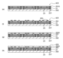
- FIG. 2 is a partially enlarged view of a region surrounded by a dashed line in FIG. 1; 1.
- the term “substantially” means that it includes a range that takes into account manufacturing tolerances, assembly variations, and the like, unless otherwise explicitly stated.
- the notation “X to Y” in the description of numerical ranges means X or more and Y or less, unless otherwise specified.
- “1 to 5% by mass” means “1% by mass or more and 5% by mass or less”.
- alkyl group includes not only alkyl groups without substituents (unsubstituted alkyl groups) but also alkyl groups with substituents (substituted alkyl groups).
- (meth)acryl used herein represents a concept that includes both acryl and methacryl. The same applies to similar notations such as "(meth)acrylate”.
- organic group as used herein means an atomic group obtained by removing one or more hydrogen atoms from an organic compound, unless otherwise specified.
- a "monovalent organic group” represents an atomic group obtained by removing one hydrogen atom from an arbitrary organic compound.
- electronic device refers to elements to which electronic engineering technology is applied, such as semiconductor chips, semiconductor elements, printed wiring boards, electric circuit display devices, information communication terminals, light-emitting diodes, physical batteries, and chemical batteries. , devices, final products, etc.
- the photosensitive resin composition of this embodiment contains a polyimide resin (A), a polyfunctional (meth)acrylate compound (B), a photosensitive agent (C), and a polymerization inhibitor (D).
- the polyimide resin (A) is a closed-ring polyimide resin containing a closed-ring imide structure represented by the following general formula (a).
- X is a divalent organic group and Y is a tetravalent organic group.
- polyamide/polyimide-based photosensitive resin compositions contain polyamide but do not contain polyimide before use (before forming a cured film). That is, conventionally, a photosensitive resin composition containing polyamide is used to form a film on a substrate, and the film is typically heated to ring-close the polyamide to form polyimide. However, in this case, the film shrinks due to the ring-closure reaction and the accompanying dehydration, and it is sometimes difficult to obtain a cured film with good flatness.
- the photosensitive resin composition of the present embodiment already contains the polyimide resin (A) before use (before forming the cured film).
- the polymerization reaction of the polyfunctional (meth)acrylate compound (B) is employed as the curing mechanism (this polymerization reaction does not involve dehydration in principle). From these matters, by forming a cured film using the photosensitive resin composition of the present embodiment, it is possible to form a cured film with small shrinkage due to heating and good flatness. In particular, it is possible to form a cured film with good flatness even on a substrate having steps.
- the photosensitive resin composition of the present embodiment it is easy to form a cured film having good heat resistance and good mechanical properties (for example, tensile elongation). Cured films in electronic devices are often required to have high heat resistance and good mechanical properties. Conventionally, however, when a resin is designed to be rigid in order to improve its heat resistance, the flexibility of the resin may be lost and mechanical properties such as elongation may be degraded. Although the details are unknown, in the photosensitive resin composition of the present embodiment, the polyfunctional (meth)acrylate compound (B) is intricately entangled with the polyimide resin (A) during curing (polymerization). , it is thought that a cured film different from conventional cured films is formed. This "entangled structure of polyimide resin and polyfunctional (meth)acrylate" is considered to be related to good heat resistance and good mechanical properties.
- the extensibility of the obtained photosensitive resin composition is improved as described above, but on the other hand, swelling of the cured portion and non-uniformity of the unexposed portion Inadequate dissolution (bridge) due to excessive dissolution, and phenomenon (foot) in which the unexposed area is not completely dissolved and remains may occur. Due to the occurrence of these defects, there is a possibility that a sufficient focus margin cannot be obtained.
- the photosensitizer (C) and the polymerization inhibitor (D) it was found that both good elongation and good focus margin can be achieved by using the photosensitizer (C) and the polymerization inhibitor (D).
- the curability of the exposed area is improved, and the generation of bridges in the development process can be suppressed while maintaining good mechanical properties. .
- the solubility of the unexposed area is improved, and the generation of feet in the development process is suppressed while maintaining good mechanical properties. can do.
- the focus margin of the photosensitive resin composition can be increased.
- the photosensitive agent (C) and the polymerization inhibitor (D) at the same time and highly controlling the ratio thereof, the cured film of the photosensitive resin composition of the present embodiment has good elongation. and a good focus margin can be achieved at the same time.
- the photosensitive resin composition of the present embodiment is preferably used for forming insulating layers in electronic devices or optical devices.
- the photosensitive resin composition of this embodiment contains a polyimide resin (A) containing a structural unit represented by general formula (a).
- X is a divalent organic group and Y is a tetravalent organic group.
- the photosensitive resin composition of the present embodiment tends to shrink less due to curing (heating) by using a polyimide resin containing a closed ring imide structure represented by the general formula (a) before curing.
- the number of moles of imide groups contained in the polyimide resin (A) is IM and the number of moles of amide groups contained in the polyimide resin (A) is AM, ⁇ IM/(IM+AM) ⁇ 100(%)
- the imidization ratio represented by is preferably 90% or more, more preferably 95% or more, and still more preferably 98% or more.
- the polyimide resin (A) is a resin having few or no ring-opening amide structures and many ring-closing imide structures.
- the imidization rate can be known, for example, from the area of the peak corresponding to the amide group or the area of the peak corresponding to the imide group in the NMR spectrum.
- the imidization rate can be known from the area of the peak corresponding to the amide group, the area of the peak corresponding to the imide group, and the like in the infrared absorption spectrum.
- the polyimide resin (A) preferably contains a polyimide resin containing a fluorine atom.
- the present inventors have found that polyimide resins containing fluorine atoms tend to have better solubility in organic solvents than polyimide resins containing no fluorine atoms. Therefore, by using a polyimide resin containing a fluorine atom, it is easy to make the property of the photosensitive resin composition varnish-like.
- the amount (mass ratio) of fluorine atoms in the polyimide resin containing fluorine atoms is, for example, 1 to 30% by mass, preferably 3 to 28% by mass, more preferably 5 to 25% by mass.
- a certain amount of fluorine atoms contained in the polyimide resin facilitates obtaining sufficient organic solvent solubility. On the other hand, from the viewpoint of balance with other performances, it is preferable that the amount of fluorine atoms is not too large.
- the mechanical properties (tensile elongation, etc.) of the cured product can be further improved.
- the polyimide resin (A) preferably has a group at its end that can react with an epoxy group to form a bond.
- groups include acid anhydride groups, hydroxy groups, amino groups, carboxy groups, and the like.
- the polyimide resin (A) has an acid anhydride group at its end.
- the acid anhydride group and the epoxy group are sufficiently easy to form a bond.
- the acid anhydride group is preferably a group having a cyclic acid anhydride skeleton.
- the "cyclic structure" herein is preferably a 5- or 6-membered ring, more preferably a 5-membered ring.
- X is a divalent organic group and Y is a tetravalent organic group.
- the divalent organic group of X and/or the tetravalent organic group of Y preferably contains an aromatic ring structure, more preferably a benzene ring structure. This tends to further increase the heat resistance.
- the divalent organic group of X and/or the tetravalent organic group of Y preferably has a structure in which 2 to 6 benzene rings are linked via a single bond or a divalent linking group.
- Examples of the divalent linking group here include an alkylene group, a fluorinated alkylene group, an ether group, and the like. Alkylene groups and fluorinated alkylene groups may be linear or branched.
- the number of carbon atoms in the divalent organic group of X is, for example, 6-30.
- the number of carbon atoms in the tetravalent organic group of Y is, for example, 6-20.
- Each of the two imide rings in general formula (a) is preferably a five-membered ring.
- the polyimide resin (A) preferably contains a polyimide resin containing a fluorine atom. This tends to increase the solubility in organic solvents. Moreover, from the viewpoint of further improving the organic solvent solubility, both X and Y are preferably fluorine atom-containing groups.
- the polyimide resin (A) more preferably contains a structural unit represented by the following general formula (aa).
- Y' represents a single bond or an alkylene group
- X has the same definition as X in formula (a).
- the alkylene group of Y' may be linear or branched. Some or all of the hydrogen atoms in the alkylene group of Y' are preferably substituted with fluorine atoms.
- the number of carbon atoms in the alkylene group of Y' is, for example, 1-6, preferably 1-4, more preferably 1-3.
- the polyimide resin (A) is typically prepared by (i) first reacting (condensation polymerization) a diamine and an acid dianhydride to synthesize a polyamide, and (ii) then imidating the polyamide (ring closure reacting), and (iii) introducing a desired functional group to the terminal of the polymer as necessary.
- Specific reaction conditions can be referred to Examples described later, the description of Patent Document 1 described above, and the like.
- the diamine is incorporated into the polymer as the divalent organic group X in general formula (a).
- the acid dianhydride is incorporated into the polymer as the tetravalent organic group Y in the general formula (a).
- one or two or more diamines can be used, and one or two or more acid dianhydrides can be used.
- Raw material diamines include, for example, 3,4′-diaminodiphenyl ether (3,4′-ODA), 4,4′-diamino-2,2′-bis(trifluoromethyl)biphenyl (TFMB), 3,3 ',5,5'-tetramethylbenzidine, 2,3,5,6-tetramethyl-1,4-phenylenediamine, 3,3'-diaminodiphenylsulfone, 3,3'dimethylbenzidine, 3,3'- Bis(trifluoromethyl)benzidine, 2,2'-bis(p-aminophenyl)hexafluoropropane, bis(trifluoromethoxy)benzidine (TFMOB), 2,2'-bis(pentafluoroethoxy)benzidine (TFEOB) , 2,2′-trifluoromethyl-4,4′-oxydianiline (OBABTF), 2-phenyl-2-trifluoromethyl-bis(p-aminophenyl)
- acid dianhydrides used as raw materials include pyromellitic anhydride (PMDA), diphenyl ether-3,3′,4,4′-tetracarboxylic dianhydride (ODPA), benzophenone-3,3′, 4,4'-tetracarboxylic dianhydride (BTDA), biphenyl-3,3',4,4'-tetracarboxylic dianhydride (BPDA), diphenylsulfone-3,3',4,4'- Tetracarboxylic dianhydride (DSDA), diphenylmethane-3,3',4,4'-tetracarboxylic dianhydride, 2,2-bis(3,4-phthalic anhydride) propane, 2,2-bis (3,4-Phthalic anhydride)-1,1,1,3,3,3-hexafluoropropane (6FDA) and the like can be mentioned.
- acid dianhydrides that can be used are not limited to these.
- the usage ratio of the diamine and the acid dianhydride is basically 1:1 in terms of molar ratio. However, one may be used in excess to obtain the desired terminal structure. Specifically, by using an excessive amount of diamine, the ends (both ends) of the polyimide resin (A) tend to become amino groups. On the other hand, when the acid dianhydride is excessively used, the ends (both ends) of the polyimide resin (A) tend to become acid anhydride groups. As described above, in the present embodiment, the polyimide resin (A) preferably has an acid anhydride group at its terminal. Therefore, in the present embodiment, it is preferable to use an excess amount of acid dianhydride when synthesizing the polyimide resin (A).
- terminal amino groups and/or acid anhydride groups of the polyimide obtained by condensation polymerization may be reacted with some kind of reagent so that the polyimide terminals have desired functional groups.
- the weight average molecular weight of the polyimide resin (A) is, for example, 5,000 to 100,000, preferably 7,000 to 75,000, more preferably 10,000 to 50,000.
- the weight average molecular weight of the polyimide resin (A) is large to some extent, for example, sufficient heat resistance of the cured film can be obtained.
- the weight average molecular weight of the polyimide resin (A) is not too large, it becomes easier to dissolve the polyimide resin (A) in the organic solvent.
- the weight average molecular weight can usually be determined by gel permeation chromatography (GPC) using polystyrene as a standard substance.
- the photosensitive resin composition of this embodiment contains a polyfunctional (meth)acrylate compound (B).
- a polyfunctional (meth)acrylate compound (B) those having two or more (meth)acryloyl groups in one molecule can be mentioned without particular limitation.
- the polyfunctional (meth)acrylate compound (B) is preferably trifunctional or higher.
- the upper limit for the number of functional groups is, for example, 11 functional groups in consideration of the availability of raw materials.
- the polyfunctional (meth)acrylate compound (B) having a large number of functional groups ((meth)acryloyl groups) is used, the chemical resistance of the cured film tends to increase.
- the polyfunctional (meth)acrylate compound (B) having a small number of functional groups ((meth)acryloyl groups) is used, mechanical properties such as tensile elongation of the cured film tend to be improved.
- the polyfunctional (meth)acrylate compound (B) preferably contains a 3- to 4-functional (meth)acrylate compound (B1).
- the polyfunctional (meth)acrylate compound (B) preferably contains a pentafunctional or higher (meth)acrylate compound (B2).
- the polyfunctional (meth)acrylate compound (B) can contain a compound represented by the following general formula (b).
- R' is a hydrogen atom or a methyl group
- n is 0 to 3
- R is a hydrogen atom or a (meth)acryloyl group.
- polyfunctional (meth)acrylate compound (B) examples include the following. Of course, polyfunctional (meth)acrylate compounds (B) are not limited to these.
- Aronix M-400, Aronix M-460, Aronix M-402, Aronix M-510, Aronix M-520 (manufactured by Toagosei Co., Ltd.), KAYARAD T-1420, KAYARAD DPHA, KAYARAD DPCA20, KAYARAD DPCA30, KAYARAD DPCA60, KAYARAD DPCA120 (manufactured by Nippon Kayaku Co., Ltd.), Viscoat #230, Viscoat #300, Viscoat #802, Viscoat #2500, Viscoat #1000, Viscoat #1080 (manufactured by Osaka Organic Chemical Industry Co., Ltd.), NK Ester A-BPE-10 , NK Ester A-GLY-9E, NK Ester A-9550, and NK Ester A-DPH (manufactured by Shin-Nakamura Chemical Co., Ltd.).
- the photosensitive resin composition may contain only one polyfunctional (meth)acrylate compound (B), or may contain two or more polyfunctional (meth)acrylate compounds (B). In the latter case, it is preferable to use together a polyfunctional (meth)acrylate compound (B) having a different number of functional groups.
- polyfunctional (meth)acrylate compounds (B) with different numbers of functional groups together, a more complex "entangled structure of polyimide and polyfunctional (meth)acrylate" can be created, resulting in better heat resistance and mechanical properties. It is considered possible.
- the amount of the polyfunctional (meth)acrylate compound (B) with respect to 100 parts by mass of the polyimide resin (A) is, for example, 25 to 150 parts by mass, preferably 50 to 120 parts by mass, more preferably 70 to 100 parts by mass, more preferably 80 to 95 parts by mass.
- the amount of the polyfunctional (meth)acrylate compound (B) used is not particularly limited, but one or more of the various properties can be enhanced by appropriately adjusting the amount used as described above.
- the entangled structure of the polyimide having a cyclic structure and the polyfunctional (meth)acrylate is formed by curing, but the polyimide resin (A By appropriately adjusting the amount of the polyfunctional (meth) acrylate compound (B) for ), the polyimide resin (A) and the polyfunctional (meth) acrylate compound (B) are sufficiently entangled, and are not involved in the entanglement. It is believed that there are fewer redundant components, resulting in better performance.
- the photosensitive resin composition of this embodiment contains a photosensitive agent (C).
- the photosensitive agent (C) is not particularly limited as long as it can generate active species by light and cure the photosensitive resin composition.
- the photosensitizer (C) preferably contains a photoradical generator.
- a photoradical generator is particularly effective for polymerizing the polyfunctional (meth)acrylate compound (B).
- the photoradical generator that can be used is not particularly limited, and known ones can be used as appropriate.
- the photosensitive resin composition may contain only 1 type of photosensitive agents (C), and may contain 2 or more types.
- the content of the photosensitive agent (C) is, for example, 5 parts by mass or more and 30 parts by mass or less, preferably 10 parts by mass or more and 25 parts by mass or less with respect to 100 parts by mass of the polyimide resin (A).
- the photosensitive resin composition of this embodiment contains a polymerization inhibitor (D).
- the polymerization inhibitor (D) includes, for example, hindered phenol compounds, hindered amine compounds, N-oxyl compounds and thioether compounds.
- hindered phenol compounds, hindered amine-based compounds, and N-oxyl compounds are preferably included from the viewpoint of improving the solubility of unexposed areas.
- hindered phenol compounds include 1,3,5-tris(3,5-di-tert-butyl-4-hydroxybenzyl)-1,3,5-triazine-2,4,6(1H, 3H,5H)-trione, 4,4′,4′′-(1-methylpropanyl-3-ylidene)tris(6-tert-butyl-m-cresol), 6,6′-di-tert-butyl- 4,4′-butylidenedi-m-cresol, pentaerythritol tetrakis[3-(3,5-di-tert-butyl-4-hydroxyphenyl)propionate] (Irganox 1010), 3,9-bis ⁇ 2-[3- (3-tert-butyl-4-hydroxy-5-methylphenyl)propionyloxy]-1,1-dimethylethyl ⁇ -2,4,8,10-tetraoxaspiro[5.5]undecane, 1,3, 5-tris(3,
- hindered amine compounds include tetrakis(1,2,2,6,6-pentamethyl-4-piperidyl)butane-1,2,3,4-tetracarboxylate, tetrakis(2,2,6,6- Tetramethyl-4-piperidyl)butane-1,2,3,4-tetracarboxylate, 1,2,3,4-butanetetracarboxylic acid and 1,2,2,6,6-pentamethyl-4-piperidinol and 3,9-bis(2-hydroxy-1,1-dimethylethyl)-2,4,8,10-tetraoxaspiro[5.5]undecane mixed ester, 1,2,3,4-butane Tetracarboxylic acid with 2,2,6,6-tetramethyl-4-piperidinol and 3,9-bis(2-hydroxy-1,1-dimethylethyl)-2,4,8,10-tetraoxaspiro[5 .5] mixed esters with undecane, bis(1,2,2,6,6
- N-oxyl compounds include 4-benzoyloxy-2,2,6,6-tetramethylpiperidinooxyl (4-benzoyloxy TEMPO), N-nitrosodiphenylamine, N-nitroso-N-phenylhydroxylamine. , 2,2,6,6-tetramethylpiperidine-1-oxyl (TEMPO), 4-hydroxy-2,2,6,6-tetramethylpiperidi-1-oxyl free radical (4-hydroxy TEMPO), sebacin acid bis(2,2,6,6-tetramethyl-4-piperidyl-1-oxyl) (bis sebacate TEMPO); These may be used individually by 1 type, or may use 2 or more types together.
- TEMPO 2,2,6,6-tetramethylpiperidine-1-oxyl
- 4-hydroxy-2,2,6,6-tetramethylpiperidi-1-oxyl free radical (4-hydroxy TEMPO)
- sebacin acid bis(2,2,6,6-tetramethyl-4-piperidyl-1-oxyl) bis sebacate TEMPO
- the thioether compounds include 2,2-bis ⁇ [3-(dodecylthio)-1-oxopropoxy]methyl ⁇ propane-1,3-diylbis[3-(dodecylthio)propionate], di(tridecyl)-3 , 3′-thiodipropionate and the like. These may be used individually by 1 type, or may use 2 or more types together.
- the content of the polymerization inhibitor (D) with respect to 100 parts by mass of the polyimide resin (A) is preferably 0.1 parts by mass or more and 5 parts by mass or less, more preferably 1 It is at least 3 parts by mass and no more than 3 parts by mass. If the content of the polymerization inhibitor (D) is within the above range, the solubility of the unexposed area is improved, and the phenomenon that the unexposed area in the development process is not completely dissolved and remains while maintaining good mechanical properties (foot ) can be suppressed.
- the content of the polymerization inhibitor (D) with respect to 100 parts by mass of the photosensitive agent (C) is preferably 1 part by mass or more and 30 parts by mass or less, more preferably 5 parts by mass. It is more than 20 parts by mass and less than 20 parts by mass. If the content of the polymerization inhibitor (D) with respect to 100 parts by mass of the photosensitive agent (C) is within the above range, the cured film of the photosensitive resin composition of the present embodiment has good elongation and a good focus margin. It is possible to achieve both.
- the photosensitive resin composition of the present embodiment preferably contains a thermal radical generator (E).
- a thermal radical generator E
- the thermal radical generator (E) for example, the heat resistance of the cured film can be further enhanced and/or the chemical resistance (resistance to organic solvents and the like) of the cured film can be enhanced. This is probably because the use of the thermal radical generator (E) further accelerates the polymerization reaction of the polyfunctional (meth)acrylate compound (B).
- the thermal radical generator (E) preferably contains an organic peroxide.
- Organic peroxides include octanoyl peroxide, lauroyl peroxide, stearoyl peroxide, 1,1,3,3-tetramethylbutylperoxy 2-ethylhexanoate, oxalic acid peroxide, 2,5-dimethyl- 2,5-di(2-ethylhexanoylperoxy)hexane, 1-cyclohexyl-1-methylethylperoxy 2-ethylhexanoate, t-hexylperoxy 2-ethylhexanoate, t-butylperoxy 2-ethylhexanoate, m-toluyl peroxide, benzoyl peroxide, benzoyl peroxide, methyl ethyl ketone peroxide, acetyl peroxide, t-butyl hydroperoxide, di-t-buty
- thermal radical generator (E) When the thermal radical generator (E) is used, only one thermal radical generator (E) may be used, or two or more thermal radical generators (E) may be used. When the thermal radical generator (E) is used, the amount thereof is preferably 0.1 parts by mass or more and 30 parts by mass or less, more preferably 1 part by mass or more and 20 parts by mass, relative to 100 parts by mass of the polyimide resin (A). It is below.
- the photosensitive resin composition of the present embodiment preferably contains a cross-linking agent (F).
- a cross-linking agent (F) By using the cross-linking agent (F), for example, the cross-linking agent (F) reacts with other components contained in the photosensitive resin composition, or the cross-linking agent (F) is polymerized with each other, and the cross-linking agent (F) becomes closely entangled with the photosensitive resin composition. This is thought to improve the chemical resistance and elongation of the resin film made of the cured product of the photosensitive resin composition.
- the cross-linking agent (F) preferably has one epoxy-containing group at one end of the molecule and one (meth)acryloyl group at the other end of the molecule.
- the "epoxy-containing group” refers to a substituent having a three-membered ether oxacyclopropane (oxirane) in its structural formula.
- oxirane a substituent having a three-membered ether oxacyclopropane (oxirane) in its structural formula.
- Specific examples thereof include an epoxy group, a glycidyl group, a glycidyl ether group, and one or more hydrogen atoms in an organic group to an epoxy group, a glycidyl group, or a glycidyl ether group (a group obtained by removing hydrogen from the OH group of glycidol).
- Substituted groups may be mentioned, and specific examples include 1,2-epoxycyclohexyl group and the like.
- organic group is not particularly limited, examples include methyl group, ethyl group, n-propyl group, isopropyl group, n-butyl group, isobutyl group, sec-butyl group, tert-butyl group, pentyl group, neopentyl group and hexyl.
- alkyl groups such as group, heptyl group, octyl group, nonyl group and decyl group; alkenyl groups such as allyl group, pentenyl group and vinyl group; alkynyl groups such as ethynyl group; alkylidene groups such as methylidene group and ethylidene group; aryl groups such as , naphthyl and anthracenyl groups; aralkyl groups such as benzyl and phenethyl groups; alkaryl groups such as tolyl and xylyl groups; or cycloalkyl groups such as adamantyl, cyclopentyl, cyclohexyl and cyclooctyl groups is mentioned.
- the cross-linking agent (F) preferably contains a compound represented by general formula (1).
- X 1 represents a (meth)acryloyl group.
- X2 represents a glycidyl group, a glycidyl ether group, an epoxy group or a 1,2-epoxycyclohexyl group as an epoxy-containing group.
- n represents an integer of 1-10.
- the reactivity between the cross-linking agent (F) and other components contained in the photosensitive resin composition or the cross-linking agent (F) is improved, and the photosensitive resin composition It is preferable because the chemical resistance and elongation of the resin film made of the cured product are improved.
- n is within the range of 1 to 10, the elongation rate of the resin film made of the cured product of the photosensitive resin composition becomes more suitable, which is preferable.
- the cross-linking agent (F) it is preferable that one or more compounds selected from compounds represented by any one of the following chemical formulas (2) to (4) be included as the compound satisfying the general formula (1).
- the chemical resistance and elongation of the resin film made of the cured product of the photosensitive resin composition are increased. You can have both in balance.
- the content of the cross-linking agent (F) is, for example, 0.1 parts by mass or more, preferably 0.5 parts by mass or more, more preferably 1 part by mass or more with respect to 100 parts by mass of the polyimide resin (A). .
- the content of the cross-linking agent (F) is 0.1 parts by mass or more, the cured product of the photosensitive resin composition can have high chemical resistance.
- the content of the cross-linking agent (F) is, for example, 30 parts by mass or less, preferably 20 parts by mass or less, more preferably 10 parts by mass or less, relative to 100 parts by mass of the polyimide resin (A).
- the content of the cross-linking agent (F) is 30 parts by mass or less, the ratio of the polyimide resin (A) in the photosensitive resin composition is maintained, and the elongation of the cured product of the photosensitive resin composition becomes good. In addition, the adhesion between the photosensitive resin composition and the substrate is sufficiently improved.
- the photosensitive resin composition of the present embodiment may contain only one type of cross-linking agent (F), or may contain two or more types.
- the photosensitive resin composition of this embodiment preferably contains a silane coupling agent (G).
- a silane coupling agent (G) for example, the adhesion between the substrate and the cured film can be further enhanced.
- silane coupling agent (G) examples include amino group-containing silane coupling agents, epoxy group-containing silane coupling agents, (meth)acryloyl group-containing silane coupling agents, mercapto group-containing silane coupling agents, vinyl group-containing Silane coupling agents such as silane coupling agents, ureido group-containing silane coupling agents, sulfide group-containing silane coupling agents, and silane coupling agents having a cyclic anhydride structure can be used.
- amino group-containing silane coupling agents include bis(2-hydroxyethyl)-3-aminopropyltriethoxysilane, ⁇ -aminopropyltriethoxysilane, ⁇ -aminopropyltrimethoxysilane, ⁇ -aminopropylmethyldiethoxysilane.
- Silane ⁇ -aminopropylmethyldimethoxysilane, N- ⁇ (aminoethyl) ⁇ -aminopropyltrimethoxysilane, N- ⁇ (aminoethyl) ⁇ -aminopropyltriethoxysilane, N- ⁇ (aminoethyl) ⁇ -amino Propylmethyldimethoxysilane, N- ⁇ (aminoethyl) ⁇ -aminopropylmethyldiethoxysilane, N-phenyl- ⁇ -amino-propyltrimethoxysilane and the like.
- epoxy group-containing silane coupling agents include ⁇ -glycidoxypropyltrimethoxysilane, ⁇ -glycidoxypropylmethyldiethoxysilane, ⁇ -(3,4-epoxycyclohexyl)ethyltrimethoxysilane, and ⁇ -glycidyl. propyltrimethoxysilane and the like.
- Examples of (meth)acryloyl group-containing silane coupling agents include ⁇ -((meth)acryloyloxypropyl)trimethoxysilane, ⁇ -((meth)acryloyloxypropyl)methyldimethoxysilane, ⁇ -((meth) acryloyloxypropyl)methyldiethoxysilane and the like.
- Mercapto group-containing silane coupling agents include, for example, 3-mercaptopropyltrimethoxysilane.
- Vinyl group-containing silane coupling agents include, for example, vinyltris( ⁇ -methoxyethoxy)silane, vinyltriethoxysilane, vinyltrimethoxysilane and the like.
- Ureido group-containing silane coupling agents include, for example, 3-ureidopropyltriethoxysilane.
- sulfide group-containing silane coupling agents include bis(3-(triethoxysilyl)propyl)disulfide and bis(3-(triethoxysilyl)propyl)tetrasulfide.
- Silane coupling agents having a cyclic anhydride structure include, for example, 3-trimethoxysilylpropylsuccinic anhydride, 3-triethoxysilylpropylsuccinic anhydride, and 3-dimethylmethoxysilylpropylsuccinic anhydride. be done.
- a silane coupling agent having a cyclic anhydride structure is particularly preferably used.
- the details are unknown, it is presumed that the cyclic anhydride structure readily reacts with the main chain, side chains and/or terminals of the polyimide resin (A), resulting in a particularly good effect of improving adhesion.
- the silane coupling agent (G) When the silane coupling agent (G) is used, it may be used alone, or two or more adhesion aids may be used in combination.
- the amount used is, for example, 0.1 to 20 parts by mass, preferably 0.3 to 15 parts by mass when the amount of polyimide resin (A) used is 100 parts by mass. parts, more preferably 0.4 to 12 parts by mass, and still more preferably 0.5 to 10 parts by mass.
- the photosensitive resin composition of the present embodiment preferably contains a curing catalyst (H).
- This curing catalyst (H) functions to accelerate the reaction of the cross-linking agent (F).
- the reaction involving the cross-linking agent (F) can proceed sufficiently, and for example, the tensile elongation of the cured film can be further improved.
- the curing catalyst (H) includes compounds known as curing catalysts for epoxy resins (often called curing accelerators). For example, diazabicycloalkenes such as 1,8-diazabicyclo[5,4,0]undecene-7 and derivatives thereof; amine compounds such as tributylamine and benzyldimethylamine; imidazole compounds such as 2-methylimidazole; triphenyl Organic phosphines such as phosphine and methyldiphenylphosphine; tetra-substituted phosphonium salts such as phosphonium/tetranaphthyloxyborate and tetraphenylphosphonium/4,4'-sulfonyldiphenolate; and triphenylphosphine obtained by adducting benzoquinone. Among them, organic phosphines are preferred.
- the curing catalyst (H) When the curing catalyst (H) is used, its amount is, for example, 1 to 80 parts by mass, preferably 2 to 50 parts by mass, more preferably 3 to 30 parts by mass with respect to 100 parts by mass of the cross-linking agent (F). .
- the photosensitive resin composition of the present embodiment preferably contains surfactant (I). This can further improve the applicability of the photosensitive resin composition and the flatness of the film.
- Surfactants (I) include fluorine-based surfactants, silicone-based surfactants, alkyl-based surfactants, and acrylic surfactants. From another point of view, the surfactant is preferably nonionic. The use of nonionic surfactants is preferable, for example, from the viewpoint of suppressing unintentional reactions with other components in the composition and enhancing the storage stability of the composition.
- Surfactant (I) preferably contains a surfactant containing at least one of a fluorine atom and a silicon atom. This contributes to obtaining a uniform resin film (improvement of coatability), improvement of developability, and improvement of adhesive strength.
- a surfactant is preferably, for example, a nonionic surfactant containing at least one of a fluorine atom and a silicon atom.
- Examples of commercially available products that can be used as the surfactant (I) include F-251, F-253, F-281, F-430, F-477, and F-251, F-253, F-281, F-430, F-477, and F-251, F-253, F-281, F-430, and F-477, manufactured by DIC Corporation.
- Fluorine-containing oligomer structure surfactants such as, fluorine-containing nonionic surfactants such as Ftergent 250 and Ftergent 251 manufactured by Neos Co., Ltd., SILFOAM (registered trademark) series manufactured by Wacker Chemie (for example, and silicone surfactants such as SD 100 TS, SD 670, SD 850, SD 860, SD 882).
- FC4430 and FC4432 manufactured by 3M are also preferable surfactants.
- the photosensitive resin composition of the present embodiment contains surfactant (I), it can contain one or more surfactants.
- the photosensitive resin composition of the present embodiment contains the surfactant (I)
- the amount thereof is, when the content of the polyimide resin (A) is 100 parts by mass, for example 0.001 to 1 part by mass, preferably is 0.005 to 0.5 parts by mass.
- the photosensitive resin composition of this embodiment preferably contains a solvent (J). Thereby, a photosensitive resin film can be easily formed on a substrate (particularly, a substrate having a step) by a coating method.
- Solvent (J) usually contains an organic solvent.
- the organic solvent is not particularly limited as long as it can dissolve or disperse each component described above and does not substantially chemically react with each component.
- organic solvents include acetone, methyl ethyl ketone, toluene, propylene glycol methyl ethyl ether, propylene glycol dimethyl ether, propylene glycol 1-monomethyl ether 2-acetate, diethylene glycol ethyl methyl ether, diethylene glycol monoethyl ether acetate, diethylene glycol monobutyl ether acetate, benzyl Alcohol, propylene carbonate, ethylene glycol diacetate, propylene glycol diacetate, propylene glycol monomethyl ether acetate, dipropylene glycol methyl-n-propyl ether, butyl acetate, ⁇ -butyrolactone, methyl lactate, ethyl lactate, butyl lactate and the like. . These may be used singly or in combination.
- the photosensitive resin composition of the present embodiment contains the solvent (J)
- the photosensitive resin composition of the present embodiment is usually in the form of varnish.
- the photosensitive resin composition of the present embodiment is preferably a varnish-like composition in which at least the polyimide resin (A) and the polyfunctional (meth)acrylate compound (B) are dissolved in the solvent (J). composition. Since the photosensitive resin composition of the present embodiment is in the form of varnish, it is possible to form a uniform film by coating. Further, since the polyimide resin (A) and the polyfunctional (meth)acrylate compound (B) are "dissolved” in the solvent (J), a homogeneous cured film can be obtained.
- the concentration of the total solid content (nonvolatile components) in the photosensitive resin composition is preferably 10 to 50% by mass, more preferably 20 to 45% by mass.
- concentration of the total solid content (nonvolatile components) in the photosensitive resin composition is preferably 10 to 50% by mass, more preferably 20 to 45% by mass.
- each component can fully be melt
- good coatability can be ensured, which in turn leads to improvement in flatness during spin coating.
- the viscosity of the photosensitive resin composition can be appropriately controlled by adjusting the content of the non-volatile component.
- the ratio of the polyimide resin (A) and the polyfunctional (meth)acrylate compound (B) in the entire composition is preferably 20 to 50% by mass.
- the photosensitive resin composition of the present embodiment may contain components other than the components listed above, if necessary.
- Such components include, for example, water, fillers such as silica, sensitizers, film-forming agents, and the like.
- the method for manufacturing an electronic device includes: A film forming step of forming a photosensitive resin film on a substrate using the photosensitive resin composition described above; an exposure step of exposing the photosensitive resin film; a developing step of developing the exposed photosensitive resin film; including. Moreover, it is preferable that the method for manufacturing an electronic device of the present embodiment includes a thermosetting step of heating and curing the exposed photosensitive resin film after the above-described developing step. Thereby, a cured film having sufficient heat resistance can be obtained. As described above, an electronic device provided with a cured film of the photosensitive resin composition of the present embodiment can be manufactured.
- FIG. 1 is a longitudinal sectional view showing an example of the electronic device of this embodiment.
- FIG. 2 is a partially enlarged view of a region surrounded by a dashed line in FIG.
- the upper side in FIG. 1 is called “upper”
- the lower side is called “lower”.
- the electronic device 1 shown in FIG. 1 has a so-called package-on-package structure including a through electrode substrate 2 and a semiconductor package 3 mounted thereon.
- the through electrode substrate 2 includes an insulating layer 21 , a plurality of through wirings 221 penetrating from the upper surface to the lower surface of the insulating layer 21 , a semiconductor chip 23 embedded inside the insulating layer 21 , and provided on the lower surface of the insulating layer 21 . an upper wiring layer 25 provided on the upper surface of the insulating layer 21; and solder bumps 26 provided on the lower surface of the lower wiring layer 24. As shown in FIG.
- the semiconductor package 3 includes a package substrate 31, a semiconductor chip 32 mounted on the package substrate 31, bonding wires 33 electrically connecting the semiconductor chip 32 and the package substrate 31, and the semiconductor chip 32 and the bonding wires 33. It has an embedded sealing layer 34 and solder bumps 35 provided on the lower surface of the package substrate 31 .
- a semiconductor package 3 is laminated on the through electrode substrate 2 . Thereby, the solder bumps 35 of the semiconductor package 3 and the upper wiring layers 25 of the through electrode substrate 2 are electrically connected.
- the through electrode substrate 2 and the semiconductor package 3 having different semiconductor chips are stacked, the mounting density per unit area can be increased. Therefore, it is possible to achieve both miniaturization and high performance.
- the through electrode substrate 2 and the semiconductor package 3 will be further detailed below.
- the lower wiring layer 24 and the upper wiring layer 25 provided in the through electrode substrate 2 shown in FIG. 2 each include an insulating layer, a wiring layer, a through wiring, and the like.
- the lower wiring layer 24 and the upper wiring layer 25 include wiring inside and on the surface, and are electrically connected to each other through the through wiring 221 penetrating the insulating layer 21 .
- a wiring layer included in the lower wiring layer 24 is connected to the semiconductor chip 23 and the solder bumps 26 . Therefore, the lower wiring layer 24 functions as a rewiring layer for the semiconductor chip 23 and the solder bumps 26 function as external terminals of the semiconductor chip 23 .
- the through wiring 221 shown in FIG. 2 is provided so as to penetrate the insulating layer 21 as described above. As a result, the lower wiring layer 24 and the upper wiring layer 25 are electrically connected, and the through electrode substrate 2 and the semiconductor package 3 can be stacked. can.
- a cured film of the photosensitive resin composition of the present embodiment can be used to form the insulating layer of the rewiring layer.
- the semiconductor chip 23 and the rewiring layer (upper wiring layer 25) provided on the surface of the semiconductor chip 23 are provided, and the insulating layer in the rewiring layer is the photosensitive layer of this embodiment. It is possible to realize an electronic device composed of a cured product of a flexible resin composition.
- the effect of reinforcing the insulating layer 21 is obtained because the through wiring 221 penetrates the insulating layer 21 . Therefore, even when the mechanical strength of the lower wiring layer 24 and the upper wiring layer 25 is low, the mechanical strength of the entire through electrode substrate 2 can be prevented from being lowered. As a result, the thickness of the lower wiring layer 24 and the upper wiring layer 25 can be further reduced, and the height of the electronic device 1 can be further reduced.
- the electronic device 1 shown in FIG. 1 also includes a through wire 222 provided so as to penetrate the insulating layer 21 located on the upper surface of the semiconductor chip 23 in addition to the through wire 221 . Thereby, electrical connection between the upper surface of the semiconductor chip 23 and the upper wiring layer 25 can be achieved.
- the insulating layer 21 is provided so as to cover the semiconductor chip 23 . This enhances the effect of protecting the semiconductor chip 23 . As a result, the reliability of the electronic device 1 can be improved. Also, the electronic device 1 can be easily applied to a mounting system such as the package-on-package structure according to the present embodiment.
- the diameter W (see FIG. 2) of the through wiring 221 is not particularly limited, but is preferably about 1 to 100 ⁇ m, more preferably about 2 to 80 ⁇ m. Thereby, the electrical conductivity of the through wiring 221 can be ensured without impairing the mechanical properties of the insulating layer 21 .
- the semiconductor package 3 shown in FIG. 1 may be any form of package.
- QFP Quad Flat Package
- SOP Small Outline Package
- BGA Bit Grid Array
- CSP Chip Size Package
- QFN Quadrature Package
- SON Small Outline Package
- Forms such as LF-BGA (Lead Flame BGA) can be mentioned.
- the arrangement of the semiconductor chips 32 is not particularly limited, as an example in FIG. 1, a plurality of semiconductor chips 32 are stacked. As a result, the mounting density is increased.
- the plurality of semiconductor chips 32 may be arranged side by side in the planar direction, or may be arranged side by side in the planar direction while being stacked in the thickness direction.
- the package substrate 31 may be any substrate, but is, for example, a substrate that includes an insulating layer, a wiring layer, a through wiring, etc. (not shown). Among them, the solder bump 35 and the bonding wire 33 can be electrically connected via the through wiring.
- the sealing layer 34 is made of, for example, a known sealing resin material. By providing such a sealing layer 34, the semiconductor chip 32 and the bonding wires 33 can be protected from external forces and the external environment.
- the semiconductor chip 23 provided in the through electrode substrate 2 and the semiconductor chip 32 provided in the semiconductor package 3 are arranged close to each other.
- one of the semiconductor chip 23 and the semiconductor chip 32 is a CPU (Central Processing Unit), a GPU (Graphics Processing Unit), an AP (Application Processor) or other computing element, and the other is a DRAM (Dynamic Random Access). Memory), flash memory, or the like, these elements can be arranged close to each other in the same device. This makes it possible to realize the electronic device 1 that achieves both high functionality and miniaturization.
- FIG. 3 is a process drawing showing a method of manufacturing the electronic device 1 shown in FIG. 4 to 6 are diagrams for explaining a method of manufacturing the electronic device 1 shown in FIG. 1, respectively.
- the method of manufacturing the electronic device 1 includes a chip placement step S1 for obtaining an insulating layer 21 so as to embed a semiconductor chip 23 and through wirings 221 and 222 provided on a substrate 202, and an upper layer on the insulating layer 21 and on the semiconductor chip 23.
- An upper wiring layer forming step S2 for forming the wiring layer 25 a substrate peeling step S3 for peeling the substrate 202, a lower wiring layer forming step S4 for forming the lower wiring layer 24, a solder bump 26 is formed, and a through electrode substrate is formed.
- 2 and a stacking step S6 of stacking the semiconductor package 3 on the through electrode substrate 2 is a stacking step S6 of stacking the semiconductor package 3 on the through electrode substrate 2 .
- the photosensitive resin varnish 5 (a varnish-like photosensitive resin composition) is placed on the insulating layer 21 and the semiconductor chip 23 to form a photosensitive resin layer 2510.
- a second curing step S28 and a through-wiring forming step S29 of forming the through-wiring 254 in the opening 424 (through-hole) are included.
- Chip placement step S1 First, as shown in FIG. 4A, a chip including a substrate 202, a semiconductor chip 23 and through wirings 221 and 222 provided on the substrate 202, and an insulating layer 21 provided so as to bury them An embedded structure 27 is prepared.
- the constituent material of the substrate 202 is not particularly limited, but examples include metal materials, glass materials, ceramic materials, semiconductor materials, organic materials, and the like. Also, the substrate 202 may be a semiconductor wafer such as a silicon wafer, a glass wafer, or the like.
- the semiconductor chip 23 is adhered onto the substrate 202 .
- a plurality of semiconductor chips 23 are arranged side by side on the same substrate 202 while being separated from each other.
- the plurality of semiconductor chips 23 may be of the same type, or may be of different types.
- the substrate 202 and the semiconductor chip 23 may be fixed via an adhesive layer (not shown) such as a die attach film.
- An interposer (not shown) may be provided between the substrate 202 and the semiconductor chip 23 as required.
- the interposer functions as a rewiring layer of the semiconductor chip 23, for example. Therefore, the interposer may have pads (not shown) for electrical connection with electrodes of the semiconductor chip 23, which will be described later. As a result, the pad spacing and arrangement pattern of the semiconductor chip 23 can be changed, and the degree of freedom in designing the electronic device 1 can be further enhanced.
- an inorganic substrate such as a silicon substrate, a ceramic substrate, or a glass substrate, an organic substrate such as a resin substrate, or the like is used.
- the insulating layer 21 may be, for example, a resin film (organic insulating layer) containing a thermosetting resin or a thermoplastic resin such as those listed as components of the photosensitive resin composition, and may be an ordinary sealing layer used in the technical field of semiconductors. It may be a stopping material.
- Examples of materials constituting the through-wirings 221 and 222 include copper or copper alloys, aluminum or aluminum alloys, gold or gold alloys, silver or silver alloys, nickel or nickel alloys, and the like.
- a chip-embedded structure 27 manufactured by a method different from the above may be prepared.
- the application of the photosensitive resin varnish 5 is performed using, for example, a spin coater, a bar coater, a spray device, an inkjet device, or the like.
- the viscosity of the photosensitive resin varnish 5 is not particularly limited, but is 10 cP to 6000 cP, preferably 20 cP to 5000 cP, more preferably 30 cP to 4000 cP.
- a thinner photosensitive resin layer 2510 (see FIG. 4D) can be formed.
- the upper wiring layer 25 can be made thinner, and the thickness of the electronic device 1 can be easily reduced.
- the viscosity of the photosensitive resin varnish 5 is, for example, a value measured using a cone-plate viscometer (TV-25, manufactured by Toki Sangyo Co., Ltd.) at a rotation speed of 100 rpm.
- the conditions for drying the photosensitive resin varnish 5 are not particularly limited, but include, for example, heating at a temperature of 80 to 150° C. for 1 to 60 minutes.
- the photosensitive resin film is the photosensitive resin composition of the present embodiment and is a resin film having photosensitivity.
- a photosensitive resin film is manufactured by applying, for example, a photosensitive resin varnish 5 onto a substrate such as a carrier film using various coating devices, and then drying the resulting coating film.
- the photosensitive resin layer 2510 is subjected to pre-exposure heat treatment as necessary.
- pre-exposure heat treatment the molecules contained in the photosensitive resin layer 2510 are stabilized, and the reaction in the first exposure step S21 described later can be stabilized.
- by heating under the heating conditions described later adverse effects on the photoacid generator due to heating can be minimized.
- the temperature of the pre-exposure heat treatment is preferably 70 to 130°C, more preferably 75 to 120°C, still more preferably 80 to 110°C. If the temperature of the pre-exposure heat treatment is lower than the lower limit, there is a risk that the pre-exposure heat treatment may fail to achieve the purpose of stabilizing molecules. On the other hand, if the temperature of the pre-exposure heat treatment exceeds the upper limit, the movement of the photo-acid generator becomes too active, and the influence that acid is less likely to be generated even when light is irradiated in the first exposure step S21 described later. becomes wider, and the processing precision of patterning may deteriorate.
- the time of the pre-exposure heat treatment is appropriately set according to the temperature of the pre-exposure heat treatment. 6 minutes. If the pre-exposure heat treatment time is less than the lower limit, the heating time will be insufficient, so there is a risk that the pre-exposure heat treatment will fail to achieve the purpose of stabilizing molecules. On the other hand, if the pre-exposure heat treatment time exceeds the above upper limit, the heating time is too long, and even if the pre-exposure heat treatment temperature is within the above range, the action of the photoacid generator is inhibited. There is a risk that it will be lost.
- the atmosphere of the heat treatment is not particularly limited. Although an inert gas atmosphere, a reducing gas atmosphere, or the like may be used, the atmosphere is selected in consideration of work efficiency and the like.
- the atmospheric pressure is not particularly limited. It may be under reduced pressure or under increased pressure, but considering work efficiency, etc., normal pressure is used.
- the normal pressure means a pressure of about 30 to 150 kPa, preferably atmospheric pressure.
- a mask 412 is placed on a predetermined region on the photosensitive resin layer 2510. Then, as shown in FIG. Then, light (activating radiation) is irradiated through a mask 412 . As a result, the photosensitive resin layer 2510 is exposed according to the pattern of the mask 412 .
- FIG. 4(d) illustrates a case where the photosensitive resin layer 2510 has so-called negative photosensitivity.
- the areas of the photosensitive resin layer 2510 corresponding to the light shielding portions of the mask 412 dissolve in the developer.
- active chemical species are generated from the photosensitive agent (C).
- the active species act as catalysts for the curing reaction.
- the amount of exposure in the exposure process is not particularly limited. 100 to 2000 mJ/cm 2 is preferred, and 200 to 1000 mJ/cm 2 is more preferred. Thereby, underexposure and overexposure in the photosensitive resin layer 2510 can be suppressed. As a result, it is possible to finally achieve high patterning precision. After that, if necessary, the photosensitive resin layer 2510 is subjected to post-exposure heat treatment.
- the temperature of the post-exposure heat treatment is not particularly limited. It is preferably 50 to 150°C, more preferably 50 to 130°C, even more preferably 55 to 120°C, and particularly preferably 60 to 110°C.
- the temperature of the post-exposure heat treatment is not particularly limited. It is preferably 50 to 150°C, more preferably 50 to 130°C, even more preferably 55 to 120°C, and particularly preferably 60 to 110°C.
- the time for the post-exposure heat treatment is appropriately set according to the temperature of the post-exposure heat treatment. At the above temperature, it is preferably 1 to 30 minutes, more preferably 2 to 20 minutes, still more preferably 3 to 15 minutes.
- the atmosphere of the post-exposure heat treatment is not particularly limited. Although an inert gas atmosphere, a reducing gas atmosphere, or the like may be used, the atmosphere is selected in consideration of work efficiency and the like.
- the atmospheric pressure of the post-exposure heat treatment is not particularly limited. It may be under reduced pressure or under increased pressure, but considering work efficiency, etc., normal pressure is used. As a result, pre-exposure heat treatment can be performed relatively easily.
- the normal pressure means a pressure of about 30 to 150 kPa, preferably atmospheric pressure.
- the developer examples include organic developer and water-soluble developer.
- the developer preferably contains an organic solvent. More specifically, the developer is preferably a developer containing an organic solvent as a main component (a developer in which 95% by mass or more of the component is an organic solvent). By developing with a developer containing an organic solvent, swelling of the pattern due to the developer can be suppressed more than in the case of developing with an alkaline developer (aqueous). That is, it is easy to obtain a finer pattern.
- ketone solvents such as cyclopentanone
- ester solvents such as propylene glycol monomethyl ether acetate (PGMEA) and butyl acetate
- ether solvents such as propylene glycol monomethyl ether, etc.
- an organic solvent developer containing only an organic solvent and containing only unavoidable impurities may be used as the developer.
- Impurities that are unavoidably contained include metal elements and moisture, but from the viewpoint of preventing contamination of electronic devices, it is better that the impurities that are unavoidably contained are as small as possible.
- the method of bringing the developer into contact with the photosensitive resin layer 2510 is not particularly limited. A generally known dipping method, paddle method, spray method, or the like can be appropriately applied.
- the time for the development process is usually in the range of about 5 to 300 seconds, preferably about 10 to 120 seconds, and is appropriately adjusted based on the film thickness of the resin film, the shape of the pattern to be formed, and the like.
- the photosensitive resin layer 2510 is subjected to a curing process (post-development heat treatment).
- Conditions for the curing treatment are not particularly limited, but the heating temperature is about 160 to 250° C. and the heating time is about 30 to 240 minutes.
- the photosensitive resin layer 2510 can be cured and the organic insulating layer 251 can be obtained while suppressing the thermal effect on the semiconductor chip 23 .
- Wiring layer forming step S24 a wiring layer 253 is formed on the organic insulating layer 251 (see FIG. 5F).
- the wiring layer 253 is formed by, for example, obtaining a metal layer using a vapor deposition method such as a sputtering method or a vacuum vapor deposition method, followed by patterning using a photolithography method and an etching method. Prior to forming the wiring layer 253, surface modification treatment such as plasma treatment may be performed.
- Second resin film placement step S25 Next, as shown in FIG. 5G, a photosensitive resin layer 2520 is obtained in the same manner as in the first resin film placement step S20. A photosensitive resin layer 2520 is arranged to cover the wiring layer 253 . After that, pre-exposure heat treatment is applied to the photosensitive resin layer 2520 as necessary.
- the processing conditions are, for example, the conditions described in the first resin film placement step S20.
- Second exposure step S26 Next, the photosensitive resin layer 2520 is exposed.
- the processing conditions are, for example, the conditions described in the first exposure step S21. After that, if necessary, the photosensitive resin layer 2520 is subjected to post-exposure heat treatment.
- the processing conditions are, for example, the conditions described in the first exposure step S21.
- Second development step S27 Next, the photosensitive resin layer 2520 is developed. Processing conditions are, for example, the conditions described in the first development step S22. As a result, openings 424 penetrating through the photosensitive resin layers 2510 and 2520 are formed (see FIG. 5(h)).
- Second curing step S28 After the development process, the photosensitive resin layer 2520 is subjected to a curing process (post-development heat treatment).
- the curing conditions are, for example, the conditions described in the first curing step S23. Thereby, the photosensitive resin layer 2520 is cured to obtain the organic insulating layer 252 (see FIG. 6(i)).
- the upper wiring layer 25 has two layers of the organic insulating layer 251 and the organic insulating layer 252 in this embodiment, it may have three or more layers. In this case, after the second curing step S28, a series of steps from the wiring layer forming step S24 to the second curing step S28 may be added repeatedly.
- a known method is used to form the through wiring 254, and for example, the following method is used.
- a seed layer (not shown) is formed on the organic insulating layer 252 .
- a seed layer is formed on the top surface of the organic insulating layer 252 as well as the inner surfaces (sides and bottom) of the opening 424 .
- a copper seed layer is used as the seed layer.
- the seed layer is formed by, for example, a sputtering method.
- the seed layer may be made of the same kind of metal as the through-wiring 254 to be formed, or may be made of a different kind of metal.
- a resist layer (not shown) is formed on a region of the seed layer (not shown) other than the opening 424 .
- the opening 424 is filled with metal. Electroplating, for example, is used for this filling. Examples of metals to be filled include copper or copper alloys, aluminum or aluminum alloys, gold or gold alloys, silver or silver alloys, nickel or nickel alloys, and the like. In this manner, the conductive material is embedded in the opening 424 to form the through wiring 254 .
- the resist layer (not shown) is removed. Furthermore, the seed layer (not shown) on the organic insulating layer 252 is removed. For this, for example, a flash etching method can be used.
- the position where the through wire 254 is formed is not limited to the illustrated position.
- Substrate peeling step S3 Next, as shown in FIG. 6(j), the substrate 202 is peeled off. As a result, the lower surface of the insulating layer 21 is exposed.
- Lower wiring layer forming step S4 Next, as shown in FIG. 6(k), a lower wiring layer 24 is formed on the lower surface side of the insulating layer 21. Next, as shown in FIG.
- the lower wiring layer 24 may be formed by any method, for example, it may be formed in the same manner as the upper wiring layer forming step S2 described above. The lower wiring layer 24 formed in this way is electrically connected to the upper wiring layer 25 via the through wiring 221 .
- solder bump formation step S5 As shown in FIG. 6L, solder bumps 26 are formed on the lower wiring layer 24 . Moreover, a protective film such as a solder resist layer may be formed on the upper wiring layer 25 and the lower wiring layer 24 as necessary.
- the through electrode substrate 2 is obtained as described above.
- the through electrode substrate 2 shown in FIG. 6(l) can be divided into a plurality of regions. Therefore, a plurality of through electrode substrates 2 can be efficiently manufactured by singulating the through electrode substrates 2 along the dashed line shown in FIG. 6(l), for example.
- a diamond cutter or the like can be used for singulation.
- Lamination step S6 Next, the semiconductor package 3 is arranged on the through electrode substrate 2 that has been divided into pieces. Thereby, the electronic device 1 shown in FIG. 1 is obtained.
- Such a method for manufacturing the electronic device 1 can be applied to wafer-level processes and panel-level processes using large-area substrates. Thereby, the manufacturing efficiency of the electronic device 1 can be improved and the cost can be reduced.
- the optical device of this embodiment is a light emitting element; wiring electrically connected to the light emitting element; and an insulating film covering the wiring,
- the insulating film is a cured film of the photosensitive resin composition.
- Optical devices include display devices such as liquid crystal displays, organic EL displays, touch panels, electronic paper, color filters, mini LED displays, and micro LED displays; light emitting devices such as LEDs, mini LEDs, micro LEDs, and laser diodes; solar cells, CMOS and the like, and can be used for rewiring layers, interlayer insulating films, sealing materials (top coats), and the like.
- the photosensitive resin composition of this embodiment can be suitably used particularly for micro LEDs.
- the photosensitive resin composition of the present embodiment is used to form a photosensitive resin film 73 on the surface of the substrate 71 having the step 710 .
- the substrate 71 is not particularly limited. Examples of the substrate 71 include silicon wafers, ceramic substrates, aluminum substrates, SiC wafers, and GaN wafers.
- the step 710 is, for example, a Cu rewiring. Of course, the step 710 may be a step other than Cu rewiring.
- the height of the step 710 is, for example, 1-10 ⁇ m, preferably 1-5 ⁇ m.
- the thickness of the photosensitive resin film 73 is, for example, 1 to 15 ⁇ m, preferably 1 to 10 ⁇ m. This thickness should be greater than the height of the step 710 .
- a method of forming the photosensitive resin film 73 a method of providing a liquid photosensitive resin composition on the substrate by a spin coating method, a spray coating method, a dipping method, a printing method, a roll coating method, an inkjet method, or the like can be used. can be mentioned.
- the method of forming the resin film is typically spin coating.
- the thickness of the photosensitive resin film 73 can be adjusted by changing the film formation conditions or by adjusting the viscosity of the photosensitive resin composition.
- the temperature for drying by heating is usually 50 to 180°C, preferably 60 to 150°C.
- the heat drying time is usually 30 to 600 seconds, preferably about 30 to 300 seconds. This heat drying can sufficiently remove the solvent in the photosensitive resin composition. Heating is typically done with a hot plate, an oven, or the like.
- Actinic rays for exposure include, for example, X-rays, electron beams, ultraviolet rays, and visible rays. In terms of wavelength, actinic rays of 200 to 500 nm are preferred.
- the light source is preferably g-line, h-line or i-line of a mercury lamp in terms of pattern resolution and ease of handling of the apparatus. Also, two or more rays may be mixed and used. A contact aligner, mirror projection or stepper is preferred as the exposure device.
- the exposure dose in the exposure step is usually 40 to 1500 mJ/cm 2 , preferably 80 to 1000 mJ/cm 2 , depending on the sensitivity of the photosensitive resin composition, the thickness of the resin film, the shape of the pattern to be obtained, etc. adjusted accordingly.
- post-exposure heating it is preferable to heat the resin film (post-exposure heating) between the exposure process and the development process. As a result, the reaction of the substance (photosensitive agent, etc.) that has been cleaved or decomposed by the exposure proceeds, and improvement of the pattern shape can be expected.
- the temperature and time of post-exposure heating are, for example, about 50 to 200° C. and about 10 to 600 seconds.
- the developing step the photosensitive resin film exposed in the exposing step is developed using a developer. As a result, a part of the photosensitive resin film 73 is removed to obtain a resin film 73A provided with the openings 75.
- the photosensitive resin composition of this embodiment is usually negative. Therefore, an opening 75 is provided in a portion corresponding to the light shielding portion of the photomask 720 .
- the development process can be carried out, for example, by a dipping method, a puddle method, a rotary spray method, or the like.
- the developer preferably contains an organic solvent. More specifically, the developer is preferably a developer containing an organic solvent as a main component (a developer in which 95% by mass or more of the component is an organic solvent).
- a developer containing an organic solvent a developer in which 95% by mass or more of the component is an organic solvent.
- ketone solvents such as cyclopentanone
- ester solvents such as propylene glycol monomethyl ether acetate (PGMEA) and butyl acetate
- ether solvents such as propylene glycol monomethyl ether, etc.
- an organic solvent developer containing only an organic solvent and containing only unavoidable impurities may be used.
- impurities that are unavoidably contained include metallic elements, but from the viewpoint of preventing contamination of electronic devices, it is better that the impurities that are unavoidably contained are as small as possible.
- the time for the development process is usually in the range of about 5 to 300 seconds, preferably about 10 to 120 seconds, and is appropriately adjusted based on the film thickness of the resin film, the shape of the pattern to be formed, and the like.
- the resin film 73A there may be a curing process for curing the resin film 73A between the developing process and the subsequent process.
- Curing can be performed, for example, by heat treatment at 150 to 250° C. for 30 to 240 minutes.
- the surface (upper surface) of the resin film 73A has good flatness even after such a curing process.
- a Cu rewiring 711 different from the step 710 (for example, a Cu rewiring) can be provided in the portion of the opening 75 provided in the development process. At this time, since the flatness of the upper surface of the resin film 73A is high, the fine Cu rewiring 711 can be provided with high precision.
- TEMPO is an abbreviation for "2,2,6,6-tetramethylpiperidine-1-oxyl”. Other abbreviations will be explained appropriately in the text.
- the temperature of the reaction liquid was raised to 180° C. in an oil bath and the reaction was carried out for 3 hours, and then cooled to room temperature to prepare a polyimide resin solution.
- the resulting white solid was vacuum dried at 200° C. to obtain a polyimide resin (A-1) having an acid anhydride group at the terminal.
- the weight average molecular weight (Mw) of the polyimide resin (A-1) measured by GPC was 49,000. Further, the imidization rate of the polyimide resin (A-1) was 98% by NMR measurement.
- Mw weight average molecular weight
- the temperature of the reaction liquid was raised to 180° C. in an oil bath and the reaction was carried out for 3 hours, and then cooled to room temperature to prepare a polyimide resin solution.
- the resulting white solid was vacuum dried at 200° C. to obtain a polyimide resin (A-3) having an acid anhydride group at its end.
- the weight average molecular weight (Mw) of the polyimide resin (A-3) measured by GPC was 49,000. Further, the imidization rate of the polyimide resin (A-3) was 98% by NMR measurement.
- the temperature of the reaction liquid was raised to 180° C. in an oil bath and the reaction was carried out for 3 hours, and then cooled to room temperature to prepare a polyimide resin solution.
- the resulting white solid was vacuum dried at 200° C. to obtain a polyimide resin (A-4) having an acid anhydride group at its end.
- the weight average molecular weight (Mw) of the polyimide resin (A-4) measured by GPC was 49,000. Further, the imidization rate of the polyimide resin (A-4) was 98% by NMR measurement.
- H-1 Tetraphenylphosphonium/4,4'-sulfonyldiphenolate
- a method for synthesizing the curing catalyst (H-1) is as follows. A separable flask equipped with a stirrer was charged with 37.5 g (0.15 mol) of 4,4′-bisphenol S and 100 mL of methanol, and dissolved with stirring at room temperature. A solution of 0 g (0.1 mol) was added. Then, a solution in which 41.9 g (0.1 mol) of tetraphenylphosphonium bromide was previously dissolved in 150 mL of methanol was added.
- ⁇ (D) polymerization inhibitor> (D-1) Irganox 1035 (manufactured by BASF, hindered phenolic compound) (D-2) Irganox 1010 (manufactured by BASF, hindered phenolic compound) (D-3) 4-benzoyloxy TEMPO (manufactured by Seiko Chemical Co., Ltd., N-oxyl compound) (D-4) 2,6-di-tert-butyl-p-cresol (manufactured by Tokyo Chemical Industry Co., Ltd., hindered phenol compound) (D-5) N,N-diphenylnitrosamide (manufactured by Tokyo Chemical Industry Co., Ltd., N-oxyl compound) (D-6) Capferon (manufactured by Tokyo Chemical Industry Co., Ltd., N-oxyl compound) (D-7) TEMPO (Tokyo Chemical Industry Co., Ltd., N-oxyl compound) (D-8) 4-hydroxy TEMPO (manufactured by
- the i-line was irradiated while changing the amount of change from 190 mJ to 550 mJ by 30 mJ/min and the focus from ⁇ 9 ⁇ m to +3 ⁇ m by the amount of change of 1 ⁇ m. After that, it was developed using cyclopentanone as a developer at 2500 rpm for 30 seconds, rinsed with PGMEA at 2500 rpm for 10 seconds, and dried by spinning for 20 seconds to obtain a film after development (negative pattern). rice field. After that, it was dried on a hot plate at 170° C. for 10 minutes, and then heat-treated at 200° C. for 120 minutes in a nitrogen atmosphere. As described above, a cured product of the photosensitive resin composition was obtained.
- the difference between the maximum value and the minimum value of focus was calculated as a focus margin for a via hole of 3 ⁇ m ⁇ without generating a foot or bridge. Described. In each example and comparative example, when the focus margin can be calculated for a plurality of exposure doses, the value of the largest focus margin is described.
- ⁇ Evaluation of tensile elongation> (Preparation of test piece for measuring tensile elongation)
- the photosensitive resin composition was spin-coated on an 8-inch silicon wafer so that the film thickness after drying was 10 ⁇ m, followed by heating at 120° C. for 3 minutes to obtain a photosensitive resin film.
- the resulting photosensitive resin film was exposed to light at 300 mJ/cm 2 with a high-pressure mercury lamp. Thereafter, the exposed resin film was immersed in cyclopentanone together with the silicon wafer for 30 seconds. After that, heat treatment was performed at 200° C. for 120 minutes in a nitrogen atmosphere. As described above, a cured product of the photosensitive resin composition was obtained.
- the obtained cured product was cut together with the silicon wafer with a dicing saw so as to have a width of 5 mm, and then separated from the substrate by being immersed in a 2 mass % hydrofluoric acid aqueous solution.
- the peeled film was dried at 60° C. for 10 hours to obtain a test piece (30 mm ⁇ 5 mm ⁇ 10 ⁇ m thick).
- the resulting test piece was subjected to a tensile test using a tensile tester (Tensilon RTC-1210A, manufactured by Orientec Co., Ltd.) in an atmosphere of 23° C. in accordance with JIS K 7161, and the tensile elongation of the test piece was measured. It was measured. The drawing speed in the tensile test was 5 mm/min. The unit of tensile elongation is %.
- Table 1 shows the composition of raw materials for each composition and the above evaluation results.
- the photosensitive resin compositions of Examples 1 to 32 had a large focus margin while having good elongation.
Abstract
La présente invention concerne : une composition de résine photosensible qui contient (A) une résine polyimide, (B) un composé multifonctionnel (méth)acrylate, (C) un agent sensibilisant et (D) un inhibiteur de polymérisation, la résine polyimide (A) comprenant une structure qui est représentée par la formule générale (a) (dans la formule générale (a), X représente un groupe organique divalent, et Y représente un groupe organique tétravalent) ; un dispositif électronique qui est pourvu d'une couche isolante qui est formée de cette composition de résine photosensible ; et un dispositif lumineux qui est pourvu d'une couche isolante qui est formée de cette composition de résine photosensible.
Priority Applications (2)
| Application Number | Priority Date | Filing Date | Title |
|---|---|---|---|
| JP2023512116A JPWO2023054381A1 (fr) | 2021-09-30 | 2022-09-27 | |
| JP2023172515A JP2024012299A (ja) | 2021-09-30 | 2023-10-04 | 感光性樹脂組成物、電子デバイスの製造方法、電子デバイスおよび光デバイス |
Applications Claiming Priority (2)
| Application Number | Priority Date | Filing Date | Title |
|---|---|---|---|
| JP2021-161640 | 2021-09-30 | ||
| JP2021161640 | 2021-09-30 |
Publications (1)
| Publication Number | Publication Date |
|---|---|
| WO2023054381A1 true WO2023054381A1 (fr) | 2023-04-06 |
Family
ID=85782748
Family Applications (1)
| Application Number | Title | Priority Date | Filing Date |
|---|---|---|---|
| PCT/JP2022/035981 WO2023054381A1 (fr) | 2021-09-30 | 2022-09-27 | Composition de résine photosensible, procédé de production de dispositif électronique, dispositif électronique et dispositif lumineux |
Country Status (3)
| Country | Link |
|---|---|
| JP (2) | JPWO2023054381A1 (fr) |
| TW (1) | TW202330724A (fr) |
| WO (1) | WO2023054381A1 (fr) |
Citations (6)
| Publication number | Priority date | Publication date | Assignee | Title |
|---|---|---|---|---|
| JP2012211988A (ja) * | 2011-03-31 | 2012-11-01 | Nippon Zeon Co Ltd | ネガ型感光性樹脂組成物および電子部品 |
| WO2018151079A1 (fr) * | 2017-02-15 | 2018-08-23 | 三菱ケミカル株式会社 | Composition de coloration photosensible, produit durci, élément d'espacement coloré et dispositif d'affichage d'image |
| JP2018203959A (ja) * | 2017-06-09 | 2018-12-27 | 日鉄ケミカル&マテリアル株式会社 | ポリイミド及び感光性樹脂組成物 |
| JP2019085431A (ja) * | 2017-11-01 | 2019-06-06 | 東レ株式会社 | 光重合性モノマー、それを用いた感光性樹脂組成物および感光性樹脂組成物の硬化膜 |
| WO2020203790A1 (fr) * | 2019-03-29 | 2020-10-08 | 太陽インキ製造株式会社 | Composition de résine photosensible et son produit durci |
| JP2021148891A (ja) * | 2020-03-18 | 2021-09-27 | 東レ株式会社 | 感光性樹脂組成物、硬化膜、表示装置及び硬化膜の製造方法 |
-
2022
- 2022-09-27 JP JP2023512116A patent/JPWO2023054381A1/ja active Pending
- 2022-09-27 WO PCT/JP2022/035981 patent/WO2023054381A1/fr active Application Filing
- 2022-09-29 TW TW111136983A patent/TW202330724A/zh unknown
-
2023
- 2023-10-04 JP JP2023172515A patent/JP2024012299A/ja active Pending
Patent Citations (6)
| Publication number | Priority date | Publication date | Assignee | Title |
|---|---|---|---|---|
| JP2012211988A (ja) * | 2011-03-31 | 2012-11-01 | Nippon Zeon Co Ltd | ネガ型感光性樹脂組成物および電子部品 |
| WO2018151079A1 (fr) * | 2017-02-15 | 2018-08-23 | 三菱ケミカル株式会社 | Composition de coloration photosensible, produit durci, élément d'espacement coloré et dispositif d'affichage d'image |
| JP2018203959A (ja) * | 2017-06-09 | 2018-12-27 | 日鉄ケミカル&マテリアル株式会社 | ポリイミド及び感光性樹脂組成物 |
| JP2019085431A (ja) * | 2017-11-01 | 2019-06-06 | 東レ株式会社 | 光重合性モノマー、それを用いた感光性樹脂組成物および感光性樹脂組成物の硬化膜 |
| WO2020203790A1 (fr) * | 2019-03-29 | 2020-10-08 | 太陽インキ製造株式会社 | Composition de résine photosensible et son produit durci |
| JP2021148891A (ja) * | 2020-03-18 | 2021-09-27 | 東レ株式会社 | 感光性樹脂組成物、硬化膜、表示装置及び硬化膜の製造方法 |
Also Published As
| Publication number | Publication date |
|---|---|
| TW202330724A (zh) | 2023-08-01 |
| JP2024012299A (ja) | 2024-01-30 |
| JPWO2023054381A1 (fr) | 2023-04-06 |
Similar Documents
| Publication | Publication Date | Title |
|---|---|---|
| JP7173103B2 (ja) | 感光性樹脂組成物、電子デバイスの製造方法および電子デバイス | |
| JP2018146964A (ja) | 感光性樹脂組成物、パターン硬化物の製造方法、硬化物、層間絶縁膜、カバーコート層、表面保護膜及び電子部品 | |
| JP2021096486A (ja) | ネガ型感光性樹脂組成物、及びそれを用いた半導体装置 | |
| JP6870724B2 (ja) | ネガ型感光性樹脂組成物、半導体装置および電子機器 | |
| WO2018179382A1 (fr) | Composition de résine photosensible, procédé de production de produit durci à motif, produit durci, film isolant intercouche, couche de revêtement de surface, film de protection de surface et composant électronique associé | |
| WO2023054381A1 (fr) | Composition de résine photosensible, procédé de production de dispositif électronique, dispositif électronique et dispositif lumineux | |
| WO2023021684A1 (fr) | Composition de résine photosensible, procédé de production de dispositif électronique, et dispositif électronique | |
| JP2022019609A (ja) | 感光性樹脂組成物、電子デバイスの製造方法、電子デバイスおよび感光性樹脂組成物の製造方法 | |
| JP7375406B2 (ja) | 感光性樹脂組成物、電子デバイスの製造方法および電子デバイス | |
| JP6707854B2 (ja) | ポジ型感光性樹脂組成物、硬化膜、保護膜、絶縁膜および電子装置 | |
| JP7392580B2 (ja) | 感光性樹脂組成物、電子デバイスの製造方法および電子デバイス | |
| WO2023021688A1 (fr) | Composition de résine photosensible, procédé de fabrication de dispositif électronique et dispositif électronique | |
| WO2024053564A1 (fr) | Composition de résine photosensible, film de résine et dispositif électronique | |
| CN112041745B (zh) | 凸块保护膜用感光性树脂组合物、半导体装置、半导体装置的制造方法和电子设备 | |
| JP7259317B2 (ja) | ネガ型感光性樹脂組成物、それを用いた半導体装置および電子機器 | |
| TW202309150A (zh) | 感光性樹脂組成物、電子裝置之製造方法及電子裝置 | |
| JP2024038630A (ja) | 感光性樹脂組成物、電子デバイスの製造方法および電子デバイス | |
| JP2021076728A (ja) | 感光性樹脂組成物、電子デバイスの製造方法および電子デバイス | |
| TW202309151A (zh) | 感光性樹脂組成物、電子裝置之製造方法及電子裝置 | |
| JP2023138254A (ja) | 感光性樹脂組成物、電子デバイスおよびその製造方法 | |
| JP2024038631A (ja) | 感光性樹脂組成物、樹脂膜、および電子装置 | |
| JP2024024808A (ja) | 感光性樹脂組成物、電子デバイスの製造方法および電子デバイス | |
| WO2018179330A1 (fr) | Composition de résine photosensible, procédé de fabrication de film durci à motifs, produit durci, film isolant intercalaire, couche de revêtement de couverture, film protecteur de surface et composant électronique | |
| WO2022270544A1 (fr) | Composition de résine photosensible négative, polymère photosensible négatif, film durci et dispositif semi-conducteur | |
| JP2019020531A (ja) | 感光性樹脂組成物、パターン硬化物の製造方法、硬化物、層間絶縁膜、カバーコート層、表面保護膜及び電子部品 |
Legal Events
| Date | Code | Title | Description |
|---|---|---|---|
| WWE | Wipo information: entry into national phase |
Ref document number: 2023512116 Country of ref document: JP |
|
| 121 | Ep: the epo has been informed by wipo that ep was designated in this application |
Ref document number: 22876247 Country of ref document: EP Kind code of ref document: A1 |