WO2023054381A1 - Photosensitive resin composition, method for producing electronic device, electronic device and light device - Google Patents
Photosensitive resin composition, method for producing electronic device, electronic device and light device Download PDFInfo
- Publication number
- WO2023054381A1 WO2023054381A1 PCT/JP2022/035981 JP2022035981W WO2023054381A1 WO 2023054381 A1 WO2023054381 A1 WO 2023054381A1 JP 2022035981 W JP2022035981 W JP 2022035981W WO 2023054381 A1 WO2023054381 A1 WO 2023054381A1
- Authority
- WO
- WIPO (PCT)
- Prior art keywords
- photosensitive resin
- resin composition
- mass
- composition according
- meth
- Prior art date
Links
- 239000011342 resin composition Substances 0.000 title claims abstract description 141
- 238000004519 manufacturing process Methods 0.000 title claims description 25
- 229920001721 polyimide Polymers 0.000 claims abstract description 109
- 239000009719 polyimide resin Substances 0.000 claims abstract description 96
- -1 acrylate compound Chemical class 0.000 claims abstract description 59
- 238000006116 polymerization reaction Methods 0.000 claims abstract description 26
- 125000000962 organic group Chemical group 0.000 claims abstract description 24
- 239000003112 inhibitor Substances 0.000 claims abstract description 18
- 239000003795 chemical substances by application Substances 0.000 claims abstract description 16
- 239000011347 resin Substances 0.000 claims description 120
- 229920005989 resin Polymers 0.000 claims description 120
- 239000000758 substrate Substances 0.000 claims description 71
- 238000000034 method Methods 0.000 claims description 62
- 238000010438 heat treatment Methods 0.000 claims description 49
- 150000001875 compounds Chemical class 0.000 claims description 29
- 239000006087 Silane Coupling Agent Substances 0.000 claims description 26
- 239000003431 cross linking reagent Substances 0.000 claims description 22
- 125000001153 fluoro group Chemical group F* 0.000 claims description 14
- 125000003647 acryloyl group Chemical group O=C([*])C([H])=C([H])[H] 0.000 claims description 12
- 230000003287 optical effect Effects 0.000 claims description 12
- 229910052731 fluorine Inorganic materials 0.000 claims description 11
- 125000005462 imide group Chemical group 0.000 claims description 8
- 150000002989 phenols Chemical class 0.000 claims description 7
- 239000003504 photosensitizing agent Substances 0.000 claims description 6
- 229920001187 thermosetting polymer Polymers 0.000 claims description 6
- 239000004593 Epoxy Substances 0.000 claims description 5
- 125000003368 amide group Chemical group 0.000 claims description 4
- 230000001235 sensitizing effect Effects 0.000 abstract 1
- 239000010410 layer Substances 0.000 description 168
- 239000004065 semiconductor Substances 0.000 description 59
- 230000008569 process Effects 0.000 description 30
- 239000003960 organic solvent Substances 0.000 description 23
- 238000011161 development Methods 0.000 description 21
- 239000000126 substance Substances 0.000 description 21
- 239000004094 surface-active agent Substances 0.000 description 19
- 238000006243 chemical reaction Methods 0.000 description 17
- 239000000203 mixture Substances 0.000 description 17
- 239000007787 solid Substances 0.000 description 17
- 239000002966 varnish Substances 0.000 description 17
- KFZMGEQAYNKOFK-UHFFFAOYSA-N Isopropanol Chemical compound CC(C)O KFZMGEQAYNKOFK-UHFFFAOYSA-N 0.000 description 16
- 239000002253 acid Substances 0.000 description 16
- 239000000047 product Substances 0.000 description 16
- NIXOWILDQLNWCW-UHFFFAOYSA-M Acrylate Chemical compound [O-]C(=O)C=C NIXOWILDQLNWCW-UHFFFAOYSA-M 0.000 description 15
- 239000004642 Polyimide Substances 0.000 description 13
- 229910000679 solder Inorganic materials 0.000 description 13
- 239000000243 solution Substances 0.000 description 13
- 125000000524 functional group Chemical group 0.000 description 12
- 125000004018 acid anhydride group Chemical group 0.000 description 11
- 239000003054 catalyst Substances 0.000 description 11
- 238000012545 processing Methods 0.000 description 11
- 150000003254 radicals Chemical class 0.000 description 11
- 235000012431 wafers Nutrition 0.000 description 11
- 230000015572 biosynthetic process Effects 0.000 description 10
- 239000010949 copper Substances 0.000 description 10
- BGTOWKSIORTVQH-UHFFFAOYSA-N cyclopentanone Chemical compound O=C1CCCC1 BGTOWKSIORTVQH-UHFFFAOYSA-N 0.000 description 10
- 239000002904 solvent Substances 0.000 description 10
- XLYOFNOQVPJJNP-UHFFFAOYSA-N water Substances O XLYOFNOQVPJJNP-UHFFFAOYSA-N 0.000 description 10
- OKKJLVBELUTLKV-UHFFFAOYSA-N Methanol Chemical compound OC OKKJLVBELUTLKV-UHFFFAOYSA-N 0.000 description 9
- GTDPSWPPOUPBNX-UHFFFAOYSA-N ac1mqpva Chemical compound CC12C(=O)OC(=O)C1(C)C1(C)C2(C)C(=O)OC1=O GTDPSWPPOUPBNX-UHFFFAOYSA-N 0.000 description 9
- 239000012298 atmosphere Substances 0.000 description 9
- 229940042596 viscoat Drugs 0.000 description 9
- NVKGJHAQGWCWDI-UHFFFAOYSA-N 4-[4-amino-2-(trifluoromethyl)phenyl]-3-(trifluoromethyl)aniline Chemical group FC(F)(F)C1=CC(N)=CC=C1C1=CC=C(N)C=C1C(F)(F)F NVKGJHAQGWCWDI-UHFFFAOYSA-N 0.000 description 8
- XUIMIQQOPSSXEZ-UHFFFAOYSA-N Silicon Chemical group [Si] XUIMIQQOPSSXEZ-UHFFFAOYSA-N 0.000 description 8
- 150000001252 acrylic acid derivatives Chemical class 0.000 description 8
- 125000002947 alkylene group Chemical group 0.000 description 8
- 238000001035 drying Methods 0.000 description 8
- LZCLXQDLBQLTDK-UHFFFAOYSA-N ethyl 2-hydroxypropanoate Chemical compound CCOC(=O)C(C)O LZCLXQDLBQLTDK-UHFFFAOYSA-N 0.000 description 8
- 229910052710 silicon Inorganic materials 0.000 description 8
- 125000003700 epoxy group Chemical group 0.000 description 7
- 230000006872 improvement Effects 0.000 description 7
- 229910052751 metal Inorganic materials 0.000 description 7
- LLHKCFNBLRBOGN-UHFFFAOYSA-N propylene glycol methyl ether acetate Chemical compound COCC(C)OC(C)=O LLHKCFNBLRBOGN-UHFFFAOYSA-N 0.000 description 7
- 239000002994 raw material Substances 0.000 description 7
- 238000003756 stirring Methods 0.000 description 7
- YEJRWHAVMIAJKC-UHFFFAOYSA-N 4-Butyrolactone Chemical compound O=C1CCCO1 YEJRWHAVMIAJKC-UHFFFAOYSA-N 0.000 description 6
- 125000000217 alkyl group Chemical group 0.000 description 6
- 150000004985 diamines Chemical class 0.000 description 6
- 230000006870 function Effects 0.000 description 6
- 238000005227 gel permeation chromatography Methods 0.000 description 6
- 125000004435 hydrogen atom Chemical group [H]* 0.000 description 6
- 239000012535 impurity Substances 0.000 description 6
- 239000000463 material Substances 0.000 description 6
- 239000012299 nitrogen atmosphere Substances 0.000 description 6
- 238000000059 patterning Methods 0.000 description 6
- 238000007789 sealing Methods 0.000 description 6
- 239000010703 silicon Substances 0.000 description 6
- QQGYZOYWNCKGEK-UHFFFAOYSA-N 5-[(1,3-dioxo-2-benzofuran-5-yl)oxy]-2-benzofuran-1,3-dione Chemical compound C1=C2C(=O)OC(=O)C2=CC(OC=2C=C3C(=O)OC(C3=CC=2)=O)=C1 QQGYZOYWNCKGEK-UHFFFAOYSA-N 0.000 description 5
- 239000004952 Polyamide Substances 0.000 description 5
- 125000003277 amino group Chemical group 0.000 description 5
- 238000000576 coating method Methods 0.000 description 5
- 230000000694 effects Effects 0.000 description 5
- 239000002184 metal Substances 0.000 description 5
- 230000000149 penetrating effect Effects 0.000 description 5
- 229920002647 polyamide Polymers 0.000 description 5
- 125000001424 substituent group Chemical group 0.000 description 5
- 238000003786 synthesis reaction Methods 0.000 description 5
- RYGMFSIKBFXOCR-UHFFFAOYSA-N Copper Chemical compound [Cu] RYGMFSIKBFXOCR-UHFFFAOYSA-N 0.000 description 4
- YCKRFDGAMUMZLT-UHFFFAOYSA-N Fluorine atom Chemical compound [F] YCKRFDGAMUMZLT-UHFFFAOYSA-N 0.000 description 4
- 238000005481 NMR spectroscopy Methods 0.000 description 4
- PXHVJJICTQNCMI-UHFFFAOYSA-N Nickel Chemical compound [Ni] PXHVJJICTQNCMI-UHFFFAOYSA-N 0.000 description 4
- 239000012295 chemical reaction liquid Substances 0.000 description 4
- 229910052802 copper Inorganic materials 0.000 description 4
- 125000006159 dianhydride group Chemical group 0.000 description 4
- 229940116333 ethyl lactate Drugs 0.000 description 4
- 238000001914 filtration Methods 0.000 description 4
- 239000011737 fluorine Substances 0.000 description 4
- 238000009413 insulation Methods 0.000 description 4
- GDOPTJXRTPNYNR-UHFFFAOYSA-N methyl-cyclopentane Natural products CC1CCCC1 GDOPTJXRTPNYNR-UHFFFAOYSA-N 0.000 description 4
- 239000011259 mixed solution Substances 0.000 description 4
- 239000003921 oil Substances 0.000 description 4
- 125000001997 phenyl group Chemical group [H]C1=C([H])C([H])=C(*)C([H])=C1[H] 0.000 description 4
- 229920000642 polymer Polymers 0.000 description 4
- 238000012360 testing method Methods 0.000 description 4
- 125000000391 vinyl group Chemical group [H]C([*])=C([H])[H] 0.000 description 4
- VTFXHGBOGGGYDO-UHFFFAOYSA-N 2,4-bis(dodecylsulfanylmethyl)-6-methylphenol Chemical compound CCCCCCCCCCCCSCC1=CC(C)=C(O)C(CSCCCCCCCCCCCC)=C1 VTFXHGBOGGGYDO-UHFFFAOYSA-N 0.000 description 3
- ZWEHNKRNPOVVGH-UHFFFAOYSA-N 2-Butanone Chemical compound CCC(C)=O ZWEHNKRNPOVVGH-UHFFFAOYSA-N 0.000 description 3
- VFBJXXJYHWLXRM-UHFFFAOYSA-N 2-[2-[3-(3,5-ditert-butyl-4-hydroxyphenyl)propanoyloxy]ethylsulfanyl]ethyl 3-(3,5-ditert-butyl-4-hydroxyphenyl)propanoate Chemical compound CC(C)(C)C1=C(O)C(C(C)(C)C)=CC(CCC(=O)OCCSCCOC(=O)CCC=2C=C(C(O)=C(C=2)C(C)(C)C)C(C)(C)C)=C1 VFBJXXJYHWLXRM-UHFFFAOYSA-N 0.000 description 3
- 125000000022 2-aminoethyl group Chemical group [H]C([*])([H])C([H])([H])N([H])[H] 0.000 description 3
- CSCPPACGZOOCGX-UHFFFAOYSA-N Acetone Chemical compound CC(C)=O CSCPPACGZOOCGX-UHFFFAOYSA-N 0.000 description 3
- DKPFZGUDAPQIHT-UHFFFAOYSA-N Butyl acetate Natural products CCCCOC(C)=O DKPFZGUDAPQIHT-UHFFFAOYSA-N 0.000 description 3
- LYCAIKOWRPUZTN-UHFFFAOYSA-N Ethylene glycol Chemical compound OCCO LYCAIKOWRPUZTN-UHFFFAOYSA-N 0.000 description 3
- YXFVVABEGXRONW-UHFFFAOYSA-N Toluene Chemical compound CC1=CC=CC=C1 YXFVVABEGXRONW-UHFFFAOYSA-N 0.000 description 3
- BGYHLZZASRKEJE-UHFFFAOYSA-N [3-[3-(3,5-ditert-butyl-4-hydroxyphenyl)propanoyloxy]-2,2-bis[3-(3,5-ditert-butyl-4-hydroxyphenyl)propanoyloxymethyl]propyl] 3-(3,5-ditert-butyl-4-hydroxyphenyl)propanoate Chemical compound CC(C)(C)C1=C(O)C(C(C)(C)C)=CC(CCC(=O)OCC(COC(=O)CCC=2C=C(C(O)=C(C=2)C(C)(C)C)C(C)(C)C)(COC(=O)CCC=2C=C(C(O)=C(C=2)C(C)(C)C)C(C)(C)C)COC(=O)CCC=2C=C(C(O)=C(C=2)C(C)(C)C)C(C)(C)C)=C1 BGYHLZZASRKEJE-UHFFFAOYSA-N 0.000 description 3
- 229910052782 aluminium Inorganic materials 0.000 description 3
- XAGFODPZIPBFFR-UHFFFAOYSA-N aluminium Chemical compound [Al] XAGFODPZIPBFFR-UHFFFAOYSA-N 0.000 description 3
- 150000008064 anhydrides Chemical class 0.000 description 3
- 125000004432 carbon atom Chemical group C* 0.000 description 3
- 239000011248 coating agent Substances 0.000 description 3
- 230000000052 comparative effect Effects 0.000 description 3
- 239000000470 constituent Substances 0.000 description 3
- 230000006866 deterioration Effects 0.000 description 3
- 238000009792 diffusion process Methods 0.000 description 3
- GYZLOYUZLJXAJU-UHFFFAOYSA-N diglycidyl ether Chemical group C1OC1COCC1CO1 GYZLOYUZLJXAJU-UHFFFAOYSA-N 0.000 description 3
- 238000007598 dipping method Methods 0.000 description 3
- 238000004090 dissolution Methods 0.000 description 3
- 238000011156 evaluation Methods 0.000 description 3
- 239000011521 glass Substances 0.000 description 3
- 125000003055 glycidyl group Chemical group C(C1CO1)* 0.000 description 3
- FUZZWVXGSFPDMH-UHFFFAOYSA-M hexanoate Chemical compound CCCCCC([O-])=O FUZZWVXGSFPDMH-UHFFFAOYSA-M 0.000 description 3
- 125000002887 hydroxy group Chemical group [H]O* 0.000 description 3
- 239000007788 liquid Substances 0.000 description 3
- 125000002496 methyl group Chemical group [H]C([H])([H])* 0.000 description 3
- 239000002736 nonionic surfactant Substances 0.000 description 3
- 150000001451 organic peroxides Chemical class 0.000 description 3
- 150000003003 phosphines Chemical class 0.000 description 3
- 229920006122 polyamide resin Polymers 0.000 description 3
- 238000004528 spin coating Methods 0.000 description 3
- 239000007921 spray Substances 0.000 description 3
- 230000008961 swelling Effects 0.000 description 3
- 230000002194 synthesizing effect Effects 0.000 description 3
- WYTZZXDRDKSJID-UHFFFAOYSA-N (3-aminopropyl)triethoxysilane Chemical compound CCO[Si](OCC)(OCC)CCCN WYTZZXDRDKSJID-UHFFFAOYSA-N 0.000 description 2
- GEWWCWZGHNIUBW-UHFFFAOYSA-N 1-(4-nitrophenyl)propan-2-one Chemical compound CC(=O)CC1=CC=C([N+]([O-])=O)C=C1 GEWWCWZGHNIUBW-UHFFFAOYSA-N 0.000 description 2
- ARXJGSRGQADJSQ-UHFFFAOYSA-N 1-methoxypropan-2-ol Chemical compound COCC(C)O ARXJGSRGQADJSQ-UHFFFAOYSA-N 0.000 description 2
- VEUMBMHMMCOFAG-UHFFFAOYSA-N 2,3-dihydrooxadiazole Chemical compound N1NC=CO1 VEUMBMHMMCOFAG-UHFFFAOYSA-N 0.000 description 2
- XMNIXWIUMCBBBL-UHFFFAOYSA-N 2-(2-phenylpropan-2-ylperoxy)propan-2-ylbenzene Chemical compound C=1C=CC=CC=1C(C)(C)OOC(C)(C)C1=CC=CC=C1 XMNIXWIUMCBBBL-UHFFFAOYSA-N 0.000 description 2
- TXBCBTDQIULDIA-UHFFFAOYSA-N 2-[[3-hydroxy-2,2-bis(hydroxymethyl)propoxy]methyl]-2-(hydroxymethyl)propane-1,3-diol Chemical compound OCC(CO)(CO)COCC(CO)(CO)CO TXBCBTDQIULDIA-UHFFFAOYSA-N 0.000 description 2
- RLHGFJMGWQXPBW-UHFFFAOYSA-N 2-hydroxy-3-(1h-imidazol-5-ylmethyl)benzamide Chemical compound NC(=O)C1=CC=CC(CC=2NC=NC=2)=C1O RLHGFJMGWQXPBW-UHFFFAOYSA-N 0.000 description 2
- ZYAASQNKCWTPKI-UHFFFAOYSA-N 3-[dimethoxy(methyl)silyl]propan-1-amine Chemical compound CO[Si](C)(OC)CCCN ZYAASQNKCWTPKI-UHFFFAOYSA-N 0.000 description 2
- SJECZPVISLOESU-UHFFFAOYSA-N 3-trimethoxysilylpropan-1-amine Chemical compound CO[Si](OC)(OC)CCCN SJECZPVISLOESU-UHFFFAOYSA-N 0.000 description 2
- VVBLNCFGVYUYGU-UHFFFAOYSA-N 4,4'-Bis(dimethylamino)benzophenone Chemical compound C1=CC(N(C)C)=CC=C1C(=O)C1=CC=C(N(C)C)C=C1 VVBLNCFGVYUYGU-UHFFFAOYSA-N 0.000 description 2
- UZFMOKQJFYMBGY-UHFFFAOYSA-N 4-hydroxy-TEMPO Chemical compound CC1(C)CC(O)CC(C)(C)N1[O] UZFMOKQJFYMBGY-UHFFFAOYSA-N 0.000 description 2
- MJEDTBDGYVATPI-UHFFFAOYSA-N 4-hydroxy-TEMPO benzoate Chemical compound C1C(C)(C)N([O])C(C)(C)CC1OC(=O)C1=CC=CC=C1 MJEDTBDGYVATPI-UHFFFAOYSA-N 0.000 description 2
- VQVIHDPBMFABCQ-UHFFFAOYSA-N 5-(1,3-dioxo-2-benzofuran-5-carbonyl)-2-benzofuran-1,3-dione Chemical compound C1=C2C(=O)OC(=O)C2=CC(C(C=2C=C3C(=O)OC(=O)C3=CC=2)=O)=C1 VQVIHDPBMFABCQ-UHFFFAOYSA-N 0.000 description 2
- 229910001316 Ag alloy Inorganic materials 0.000 description 2
- 229910000838 Al alloy Inorganic materials 0.000 description 2
- 229910001020 Au alloy Inorganic materials 0.000 description 2
- 239000004342 Benzoyl peroxide Substances 0.000 description 2
- OMPJBNCRMGITSC-UHFFFAOYSA-N Benzoylperoxide Chemical compound C=1C=CC=CC=1C(=O)OOC(=O)C1=CC=CC=C1 OMPJBNCRMGITSC-UHFFFAOYSA-N 0.000 description 2
- NLZUEZXRPGMBCV-UHFFFAOYSA-N Butylhydroxytoluene Chemical compound CC1=CC(C(C)(C)C)=C(O)C(C(C)(C)C)=C1 NLZUEZXRPGMBCV-UHFFFAOYSA-N 0.000 description 2
- 229910000881 Cu alloy Inorganic materials 0.000 description 2
- RTZKZFJDLAIYFH-UHFFFAOYSA-N Diethyl ether Chemical compound CCOCC RTZKZFJDLAIYFH-UHFFFAOYSA-N 0.000 description 2
- KRHYYFGTRYWZRS-UHFFFAOYSA-N Fluorane Chemical compound F KRHYYFGTRYWZRS-UHFFFAOYSA-N 0.000 description 2
- UBUCNCOMADRQHX-UHFFFAOYSA-N N-Nitrosodiphenylamine Chemical compound C=1C=CC=CC=1N(N=O)C1=CC=CC=C1 UBUCNCOMADRQHX-UHFFFAOYSA-N 0.000 description 2
- 229910000990 Ni alloy Inorganic materials 0.000 description 2
- MUBZPKHOEPUJKR-UHFFFAOYSA-N Oxalic acid Natural products OC(=O)C(O)=O MUBZPKHOEPUJKR-UHFFFAOYSA-N 0.000 description 2
- XYFCBTPGUUZFHI-UHFFFAOYSA-N Phosphine Chemical compound P XYFCBTPGUUZFHI-UHFFFAOYSA-N 0.000 description 2
- 206010034972 Photosensitivity reaction Diseases 0.000 description 2
- ATUOYWHBWRKTHZ-UHFFFAOYSA-N Propane Chemical compound CCC ATUOYWHBWRKTHZ-UHFFFAOYSA-N 0.000 description 2
- VYPSYNLAJGMNEJ-UHFFFAOYSA-N Silicium dioxide Chemical compound O=[Si]=O VYPSYNLAJGMNEJ-UHFFFAOYSA-N 0.000 description 2
- BQCADISMDOOEFD-UHFFFAOYSA-N Silver Chemical compound [Ag] BQCADISMDOOEFD-UHFFFAOYSA-N 0.000 description 2
- QYTDEUPAUMOIOP-UHFFFAOYSA-N TEMPO Chemical group CC1(C)CCCC(C)(C)N1[O] QYTDEUPAUMOIOP-UHFFFAOYSA-N 0.000 description 2
- 125000003118 aryl group Chemical group 0.000 description 2
- 235000019400 benzoyl peroxide Nutrition 0.000 description 2
- 125000001951 carbamoylamino group Chemical group C(N)(=O)N* 0.000 description 2
- 239000000919 ceramic Substances 0.000 description 2
- 230000008859 change Effects 0.000 description 2
- 238000004891 communication Methods 0.000 description 2
- 238000011109 contamination Methods 0.000 description 2
- 125000004122 cyclic group Chemical group 0.000 description 2
- 230000018044 dehydration Effects 0.000 description 2
- 238000006297 dehydration reaction Methods 0.000 description 2
- ZQMIGQNCOMNODD-UHFFFAOYSA-N diacetyl peroxide Chemical compound CC(=O)OOC(C)=O ZQMIGQNCOMNODD-UHFFFAOYSA-N 0.000 description 2
- XBDQKXXYIPTUBI-UHFFFAOYSA-N dimethylselenoniopropionate Natural products CCC(O)=O XBDQKXXYIPTUBI-UHFFFAOYSA-N 0.000 description 2
- 239000003759 ester based solvent Substances 0.000 description 2
- 150000002148 esters Chemical class 0.000 description 2
- 238000005530 etching Methods 0.000 description 2
- 239000004210 ether based solvent Substances 0.000 description 2
- ANSXAPJVJOKRDJ-UHFFFAOYSA-N furo[3,4-f][2]benzofuran-1,3,5,7-tetrone Chemical compound C1=C2C(=O)OC(=O)C2=CC2=C1C(=O)OC2=O ANSXAPJVJOKRDJ-UHFFFAOYSA-N 0.000 description 2
- 239000007789 gas Substances 0.000 description 2
- PCHJSUWPFVWCPO-UHFFFAOYSA-N gold Chemical compound [Au] PCHJSUWPFVWCPO-UHFFFAOYSA-N 0.000 description 2
- 229910052737 gold Inorganic materials 0.000 description 2
- 239000010931 gold Substances 0.000 description 2
- 239000003353 gold alloy Substances 0.000 description 2
- 239000011261 inert gas Substances 0.000 description 2
- 239000005453 ketone based solvent Substances 0.000 description 2
- 125000005647 linker group Chemical group 0.000 description 2
- QSHDDOUJBYECFT-UHFFFAOYSA-N mercury Chemical compound [Hg] QSHDDOUJBYECFT-UHFFFAOYSA-N 0.000 description 2
- 229910052753 mercury Inorganic materials 0.000 description 2
- VNWKTOKETHGBQD-UHFFFAOYSA-N methane Chemical compound C VNWKTOKETHGBQD-UHFFFAOYSA-N 0.000 description 2
- 230000004048 modification Effects 0.000 description 2
- 238000012986 modification Methods 0.000 description 2
- 229910052759 nickel Inorganic materials 0.000 description 2
- 150000002894 organic compounds Chemical class 0.000 description 2
- WXZMFSXDPGVJKK-UHFFFAOYSA-N pentaerythritol Chemical compound OCC(CO)(CO)CO WXZMFSXDPGVJKK-UHFFFAOYSA-N 0.000 description 2
- 230000036211 photosensitivity Effects 0.000 description 2
- 238000012643 polycondensation polymerization Methods 0.000 description 2
- 229920001296 polysiloxane Polymers 0.000 description 2
- 239000002244 precipitate Substances 0.000 description 2
- 238000002360 preparation method Methods 0.000 description 2
- 229940116351 sebacate Drugs 0.000 description 2
- CXMXRPHRNRROMY-UHFFFAOYSA-L sebacate(2-) Chemical compound [O-]C(=O)CCCCCCCCC([O-])=O CXMXRPHRNRROMY-UHFFFAOYSA-L 0.000 description 2
- 229910052709 silver Inorganic materials 0.000 description 2
- 239000004332 silver Substances 0.000 description 2
- 238000004544 sputter deposition Methods 0.000 description 2
- 230000000087 stabilizing effect Effects 0.000 description 2
- 238000009864 tensile test Methods 0.000 description 2
- USFPINLPPFWTJW-UHFFFAOYSA-N tetraphenylphosphonium Chemical compound C1=CC=CC=C1[P+](C=1C=CC=CC=1)(C=1C=CC=CC=1)C1=CC=CC=C1 USFPINLPPFWTJW-UHFFFAOYSA-N 0.000 description 2
- 125000000101 thioether group Chemical group 0.000 description 2
- 150000003568 thioethers Chemical class 0.000 description 2
- 125000003396 thiol group Chemical group [H]S* 0.000 description 2
- YRHRIQCWCFGUEQ-UHFFFAOYSA-N thioxanthen-9-one Chemical compound C1=CC=C2C(=O)C3=CC=CC=C3SC2=C1 YRHRIQCWCFGUEQ-UHFFFAOYSA-N 0.000 description 2
- BPSIOYPQMFLKFR-UHFFFAOYSA-N trimethoxy-[3-(oxiran-2-ylmethoxy)propyl]silane Chemical compound CO[Si](OC)(OC)CCCOCC1CO1 BPSIOYPQMFLKFR-UHFFFAOYSA-N 0.000 description 2
- RIOQSEWOXXDEQQ-UHFFFAOYSA-N triphenylphosphine Chemical compound C1=CC=CC=C1P(C=1C=CC=CC=1)C1=CC=CC=C1 RIOQSEWOXXDEQQ-UHFFFAOYSA-N 0.000 description 2
- RSJKGSCJYJTIGS-UHFFFAOYSA-N undecane Chemical compound CCCCCCCCCCC RSJKGSCJYJTIGS-UHFFFAOYSA-N 0.000 description 2
- 238000007740 vapor deposition Methods 0.000 description 2
- NWPIOULNZLJZHU-UHFFFAOYSA-N (1,2,2,6,6-pentamethylpiperidin-4-yl) 2-methylprop-2-enoate Chemical compound CN1C(C)(C)CC(OC(=O)C(C)=C)CC1(C)C NWPIOULNZLJZHU-UHFFFAOYSA-N 0.000 description 1
- FVQMJJQUGGVLEP-UHFFFAOYSA-N (2-methylpropan-2-yl)oxy 2-ethylhexaneperoxoate Chemical compound CCCCC(CC)C(=O)OOOC(C)(C)C FVQMJJQUGGVLEP-UHFFFAOYSA-N 0.000 description 1
- PTPLXVHPKMTVIW-FPLPWBNLSA-N (Z)-hydroxyimino-oxido-phenylazanium Chemical compound O\N=[N+](/[O-])c1ccccc1 PTPLXVHPKMTVIW-FPLPWBNLSA-N 0.000 description 1
- QYGBYAQGBVHMDD-XQRVVYSFSA-N (z)-2-cyano-3-thiophen-2-ylprop-2-enoic acid Chemical compound OC(=O)C(\C#N)=C/C1=CC=CS1 QYGBYAQGBVHMDD-XQRVVYSFSA-N 0.000 description 1
- NWHNXXMYEICZAT-UHFFFAOYSA-N 1,2,2,6,6-pentamethylpiperidin-4-ol Chemical compound CN1C(C)(C)CC(O)CC1(C)C NWHNXXMYEICZAT-UHFFFAOYSA-N 0.000 description 1
- LEEANUDEDHYDTG-UHFFFAOYSA-N 1,2-dimethoxypropane Chemical compound COCC(C)OC LEEANUDEDHYDTG-UHFFFAOYSA-N 0.000 description 1
- MSAHTMIQULFMRG-UHFFFAOYSA-N 1,2-diphenyl-2-propan-2-yloxyethanone Chemical compound C=1C=CC=CC=1C(OC(C)C)C(=O)C1=CC=CC=C1 MSAHTMIQULFMRG-UHFFFAOYSA-N 0.000 description 1
- VNQNXQYZMPJLQX-UHFFFAOYSA-N 1,3,5-tris[(3,5-ditert-butyl-4-hydroxyphenyl)methyl]-1,3,5-triazinane-2,4,6-trione Chemical compound CC(C)(C)C1=C(O)C(C(C)(C)C)=CC(CN2C(N(CC=3C=C(C(O)=C(C=3)C(C)(C)C)C(C)(C)C)C(=O)N(CC=3C=C(C(O)=C(C=3)C(C)(C)C)C(C)(C)C)C2=O)=O)=C1 VNQNXQYZMPJLQX-UHFFFAOYSA-N 0.000 description 1
- YJTKZCDBKVTVBY-UHFFFAOYSA-N 1,3-Diphenylbenzene Chemical group C1=CC=CC=C1C1=CC=CC(C=2C=CC=CC=2)=C1 YJTKZCDBKVTVBY-UHFFFAOYSA-N 0.000 description 1
- AZQWKYJCGOJGHM-UHFFFAOYSA-N 1,4-benzoquinone Chemical compound O=C1C=CC(=O)C=C1 AZQWKYJCGOJGHM-UHFFFAOYSA-N 0.000 description 1
- DKEGCUDAFWNSSO-UHFFFAOYSA-N 1,8-dibromooctane Chemical compound BrCCCCCCCCBr DKEGCUDAFWNSSO-UHFFFAOYSA-N 0.000 description 1
- XDGSIIBFQCVQPU-UHFFFAOYSA-N 1-(1,1,2,2,2-pentafluoroethyl)cyclohexa-3,5-diene-1,3-diamine Chemical compound NC1=CC=CC(N)(C(F)(F)C(F)(F)F)C1 XDGSIIBFQCVQPU-UHFFFAOYSA-N 0.000 description 1
- BBHKJYQVKZWEDW-UHFFFAOYSA-N 1-(1,1,2,2,3,3,3-heptafluoropropyl)cyclohexa-3,5-diene-1,3-diamine Chemical compound NC1=CC=CC(N)(C(F)(F)C(F)(F)C(F)(F)F)C1 BBHKJYQVKZWEDW-UHFFFAOYSA-N 0.000 description 1
- UICXTANXZJJIBC-UHFFFAOYSA-N 1-(1-hydroperoxycyclohexyl)peroxycyclohexan-1-ol Chemical compound C1CCCCC1(O)OOC1(OO)CCCCC1 UICXTANXZJJIBC-UHFFFAOYSA-N 0.000 description 1
- 239000012956 1-hydroxycyclohexylphenyl-ketone Substances 0.000 description 1
- QZYOLNVEVYIPHV-UHFFFAOYSA-N 1-methyl-3-(3-methylphenyl)peroxybenzene Chemical compound CC1=CC=CC(OOC=2C=C(C)C=CC=2)=C1 QZYOLNVEVYIPHV-UHFFFAOYSA-N 0.000 description 1
- VDVUCLWJZJHFAV-UHFFFAOYSA-N 2,2,6,6-tetramethylpiperidin-4-ol Chemical compound CC1(C)CC(O)CC(C)(C)N1 VDVUCLWJZJHFAV-UHFFFAOYSA-N 0.000 description 1
- PIZHFBODNLEQBL-UHFFFAOYSA-N 2,2-diethoxy-1-phenylethanone Chemical compound CCOC(OCC)C(=O)C1=CC=CC=C1 PIZHFBODNLEQBL-UHFFFAOYSA-N 0.000 description 1
- KWVGIHKZDCUPEU-UHFFFAOYSA-N 2,2-dimethoxy-2-phenylacetophenone Chemical compound C=1C=CC=CC=1C(OC)(OC)C(=O)C1=CC=CC=C1 KWVGIHKZDCUPEU-UHFFFAOYSA-N 0.000 description 1
- WCZNKVPCIFMXEQ-UHFFFAOYSA-N 2,3,5,6-tetramethylbenzene-1,4-diamine Chemical compound CC1=C(C)C(N)=C(C)C(C)=C1N WCZNKVPCIFMXEQ-UHFFFAOYSA-N 0.000 description 1
- DPGYCJUCJYUHTM-UHFFFAOYSA-N 2,4,4-trimethylpentan-2-yloxy 2-ethylhexaneperoxoate Chemical compound CCCCC(CC)C(=O)OOOC(C)(C)CC(C)(C)C DPGYCJUCJYUHTM-UHFFFAOYSA-N 0.000 description 1
- BTJPUDCSZVCXFQ-UHFFFAOYSA-N 2,4-diethylthioxanthen-9-one Chemical compound C1=CC=C2C(=O)C3=CC(CC)=CC(CC)=C3SC2=C1 BTJPUDCSZVCXFQ-UHFFFAOYSA-N 0.000 description 1
- LCHAFMWSFCONOO-UHFFFAOYSA-N 2,4-dimethylthioxanthen-9-one Chemical compound C1=CC=C2C(=O)C3=CC(C)=CC(C)=C3SC2=C1 LCHAFMWSFCONOO-UHFFFAOYSA-N 0.000 description 1
- CEQNIRIQYOUDCF-UHFFFAOYSA-N 2,5-bis(trifluoromethyl)benzene-1,4-diamine Chemical compound NC1=CC(C(F)(F)F)=C(N)C=C1C(F)(F)F CEQNIRIQYOUDCF-UHFFFAOYSA-N 0.000 description 1
- HOKCZAUZPYGTJG-UHFFFAOYSA-N 2-(2,2,6,6-tetramethylpiperidin-4-yl)hexadecanoic acid Chemical compound CCCCCCCCCCCCCCC(C(O)=O)C1CC(C)(C)NC(C)(C)C1 HOKCZAUZPYGTJG-UHFFFAOYSA-N 0.000 description 1
- PYHYPLDLZPFMJN-UHFFFAOYSA-N 2-(2,2,6,6-tetramethylpiperidin-4-yl)octadecanoic acid Chemical compound CCCCCCCCCCCCCCCCC(C(O)=O)C1CC(C)(C)NC(C)(C)C1 PYHYPLDLZPFMJN-UHFFFAOYSA-N 0.000 description 1
- JKQRNTIBBOTABS-UHFFFAOYSA-N 2-(2,4-dichlorophenyl)-1-[2-(2,4-dichlorophenyl)-4,5-diphenylimidazol-2-yl]-4,5-diphenylimidazole Chemical compound ClC1=CC(Cl)=CC=C1C(N1C2(N=C(C(=N2)C=2C=CC=CC=2)C=2C=CC=CC=2)C=2C(=CC(Cl)=CC=2)Cl)=NC(C=2C=CC=CC=2)=C1C1=CC=CC=C1 JKQRNTIBBOTABS-UHFFFAOYSA-N 0.000 description 1
- DBUMQODMPXCGAY-UHFFFAOYSA-N 2-(2-butan-2-yloxypropoxy)propan-1-ol Chemical compound CCC(C)OC(C)COC(C)CO DBUMQODMPXCGAY-UHFFFAOYSA-N 0.000 description 1
- VXQBJTKSVGFQOL-UHFFFAOYSA-N 2-(2-butoxyethoxy)ethyl acetate Chemical compound CCCCOCCOCCOC(C)=O VXQBJTKSVGFQOL-UHFFFAOYSA-N 0.000 description 1
- MHDULSOPQSUKBQ-UHFFFAOYSA-N 2-(2-chlorophenyl)-1-[2-(2-chlorophenyl)-4,5-diphenylimidazol-2-yl]-4,5-diphenylimidazole Chemical compound ClC1=CC=CC=C1C(N1C2(N=C(C(=N2)C=2C=CC=CC=2)C=2C=CC=CC=2)C=2C(=CC=CC=2)Cl)=NC(C=2C=CC=CC=2)=C1C1=CC=CC=C1 MHDULSOPQSUKBQ-UHFFFAOYSA-N 0.000 description 1
- FPZWZCWUIYYYBU-UHFFFAOYSA-N 2-(2-ethoxyethoxy)ethyl acetate Chemical compound CCOCCOCCOC(C)=O FPZWZCWUIYYYBU-UHFFFAOYSA-N 0.000 description 1
- NLNVSTLNDJGLTL-UHFFFAOYSA-N 2-(4-ethoxynaphthalen-1-yl)-4,6-bis(trichloromethyl)-1,3,5-triazine Chemical compound C12=CC=CC=C2C(OCC)=CC=C1C1=NC(C(Cl)(Cl)Cl)=NC(C(Cl)(Cl)Cl)=N1 NLNVSTLNDJGLTL-UHFFFAOYSA-N 0.000 description 1
- FVNIIPIYHHEXQA-UHFFFAOYSA-N 2-(4-methoxynaphthalen-1-yl)-4,6-bis(trichloromethyl)-1,3,5-triazine Chemical compound C12=CC=CC=C2C(OC)=CC=C1C1=NC(C(Cl)(Cl)Cl)=NC(C(Cl)(Cl)Cl)=N1 FVNIIPIYHHEXQA-UHFFFAOYSA-N 0.000 description 1
- QRHHZFRCJDAUNA-UHFFFAOYSA-N 2-(4-methoxyphenyl)-4,6-bis(trichloromethyl)-1,3,5-triazine Chemical compound C1=CC(OC)=CC=C1C1=NC(C(Cl)(Cl)Cl)=NC(C(Cl)(Cl)Cl)=N1 QRHHZFRCJDAUNA-UHFFFAOYSA-N 0.000 description 1
- GJKGAPPUXSSCFI-UHFFFAOYSA-N 2-Hydroxy-4'-(2-hydroxyethoxy)-2-methylpropiophenone Chemical compound CC(C)(O)C(=O)C1=CC=C(OCCO)C=C1 GJKGAPPUXSSCFI-UHFFFAOYSA-N 0.000 description 1
- HSDVRWZKEDRBAG-UHFFFAOYSA-N 2-[1-(oxiran-2-ylmethoxy)hexoxymethyl]oxirane Chemical compound C1OC1COC(CCCCC)OCC1CO1 HSDVRWZKEDRBAG-UHFFFAOYSA-N 0.000 description 1
- WMYINDVYGQKYMI-UHFFFAOYSA-N 2-[2,2-bis(hydroxymethyl)butoxymethyl]-2-ethylpropane-1,3-diol Chemical compound CCC(CO)(CO)COCC(CC)(CO)CO WMYINDVYGQKYMI-UHFFFAOYSA-N 0.000 description 1
- BPZIYBJCZRUDEG-UHFFFAOYSA-N 2-[3-(1-hydroxy-2-methylpropan-2-yl)-2,4,8,10-tetraoxaspiro[5.5]undecan-9-yl]-2-methylpropan-1-ol Chemical compound C1OC(C(C)(CO)C)OCC21COC(C(C)(C)CO)OC2 BPZIYBJCZRUDEG-UHFFFAOYSA-N 0.000 description 1
- JTXMVXSTHSMVQF-UHFFFAOYSA-N 2-acetyloxyethyl acetate Chemical compound CC(=O)OCCOC(C)=O JTXMVXSTHSMVQF-UHFFFAOYSA-N 0.000 description 1
- FGTYTUFKXYPTML-UHFFFAOYSA-N 2-benzoylbenzoic acid Chemical compound OC(=O)C1=CC=CC=C1C(=O)C1=CC=CC=C1 FGTYTUFKXYPTML-UHFFFAOYSA-N 0.000 description 1
- ZCDADJXRUCOCJE-UHFFFAOYSA-N 2-chlorothioxanthen-9-one Chemical compound C1=CC=C2C(=O)C3=CC(Cl)=CC=C3SC2=C1 ZCDADJXRUCOCJE-UHFFFAOYSA-N 0.000 description 1
- MDECFHKUSHRPOX-UHFFFAOYSA-N 2-cyclohexylpropan-2-yloxy 2-ethylhexaneperoxoate Chemical compound CCCCC(CC)C(=O)OOOC(C)(C)C1CCCCC1 MDECFHKUSHRPOX-UHFFFAOYSA-N 0.000 description 1
- KMNCBSZOIQAUFX-UHFFFAOYSA-N 2-ethoxy-1,2-diphenylethanone Chemical compound C=1C=CC=CC=1C(OCC)C(=O)C1=CC=CC=C1 KMNCBSZOIQAUFX-UHFFFAOYSA-N 0.000 description 1
- ZKCCKKDTLQTPKF-UHFFFAOYSA-N 2-ethoxy-1-methoxypropane Chemical compound CCOC(C)COC ZKCCKKDTLQTPKF-UHFFFAOYSA-N 0.000 description 1
- YJQMXVDKXSQCDI-UHFFFAOYSA-N 2-ethylthioxanthen-9-one Chemical compound C1=CC=C2C(=O)C3=CC(CC)=CC=C3SC2=C1 YJQMXVDKXSQCDI-UHFFFAOYSA-N 0.000 description 1
- WFUGQJXVXHBTEM-UHFFFAOYSA-N 2-hydroperoxy-2-(2-hydroperoxybutan-2-ylperoxy)butane Chemical compound CCC(C)(OO)OOC(C)(CC)OO WFUGQJXVXHBTEM-UHFFFAOYSA-N 0.000 description 1
- PCKZAVNWRLEHIP-UHFFFAOYSA-N 2-hydroxy-1-[4-[[4-(2-hydroxy-2-methylpropanoyl)phenyl]methyl]phenyl]-2-methylpropan-1-one Chemical compound C1=CC(C(=O)C(C)(O)C)=CC=C1CC1=CC=C(C(=O)C(C)(C)O)C=C1 PCKZAVNWRLEHIP-UHFFFAOYSA-N 0.000 description 1
- XMLYCEVDHLAQEL-UHFFFAOYSA-N 2-hydroxy-2-methyl-1-phenylpropan-1-one Chemical compound CC(C)(O)C(=O)C1=CC=CC=C1 XMLYCEVDHLAQEL-UHFFFAOYSA-N 0.000 description 1
- BQZJOQXSCSZQPS-UHFFFAOYSA-N 2-methoxy-1,2-diphenylethanone Chemical compound C=1C=CC=CC=1C(OC)C(=O)C1=CC=CC=C1 BQZJOQXSCSZQPS-UHFFFAOYSA-N 0.000 description 1
- LWRBVKNFOYUCNP-UHFFFAOYSA-N 2-methyl-1-(4-methylsulfanylphenyl)-2-morpholin-4-ylpropan-1-one Chemical compound C1=CC(SC)=CC=C1C(=O)C(C)(C)N1CCOCC1 LWRBVKNFOYUCNP-UHFFFAOYSA-N 0.000 description 1
- LXBGSDVWAMZHDD-UHFFFAOYSA-N 2-methyl-1h-imidazole Chemical compound CC1=NC=CN1 LXBGSDVWAMZHDD-UHFFFAOYSA-N 0.000 description 1
- ZFQSDRHCQNFDGT-UHFFFAOYSA-N 2-methyl-6-(octylsulfanylmethyl)phenol Chemical compound CCCCCCCCSCC1=CC=CC(C)=C1O ZFQSDRHCQNFDGT-UHFFFAOYSA-N 0.000 description 1
- MWDGNKGKLOBESZ-UHFFFAOYSA-N 2-oxooctanal Chemical compound CCCCCCC(=O)C=O MWDGNKGKLOBESZ-UHFFFAOYSA-N 0.000 description 1
- 125000000094 2-phenylethyl group Chemical group [H]C1=C([H])C([H])=C(C([H])=C1[H])C([H])([H])C([H])([H])* 0.000 description 1
- KTALPKYXQZGAEG-UHFFFAOYSA-N 2-propan-2-ylthioxanthen-9-one Chemical compound C1=CC=C2C(=O)C3=CC(C(C)C)=CC=C3SC2=C1 KTALPKYXQZGAEG-UHFFFAOYSA-N 0.000 description 1
- 125000003903 2-propenyl group Chemical group [H]C([*])([H])C([H])=C([H])[H] 0.000 description 1
- PFANXOISJYKQRP-UHFFFAOYSA-N 2-tert-butyl-4-[1-(5-tert-butyl-4-hydroxy-2-methylphenyl)butyl]-5-methylphenol Chemical compound C=1C(C(C)(C)C)=C(O)C=C(C)C=1C(CCC)C1=CC(C(C)(C)C)=C(O)C=C1C PFANXOISJYKQRP-UHFFFAOYSA-N 0.000 description 1
- UAIUNKRWKOVEES-UHFFFAOYSA-N 3,3',5,5'-tetramethylbenzidine Chemical compound CC1=C(N)C(C)=CC(C=2C=C(C)C(N)=C(C)C=2)=C1 UAIUNKRWKOVEES-UHFFFAOYSA-N 0.000 description 1
- NUIURNJTPRWVAP-UHFFFAOYSA-N 3,3'-Dimethylbenzidine Chemical compound C1=C(N)C(C)=CC(C=2C=C(C)C(N)=CC=2)=C1 NUIURNJTPRWVAP-UHFFFAOYSA-N 0.000 description 1
- FRIBMENBGGCKPD-UHFFFAOYSA-N 3-(2,3-dimethoxyphenyl)prop-2-enal Chemical compound COC1=CC=CC(C=CC=O)=C1OC FRIBMENBGGCKPD-UHFFFAOYSA-N 0.000 description 1
- LJGHYPLBDBRCRZ-UHFFFAOYSA-N 3-(3-aminophenyl)sulfonylaniline Chemical compound NC1=CC=CC(S(=O)(=O)C=2C=C(N)C=CC=2)=C1 LJGHYPLBDBRCRZ-UHFFFAOYSA-N 0.000 description 1
- GXDMUOPCQNLBCZ-UHFFFAOYSA-N 3-(3-triethoxysilylpropyl)oxolane-2,5-dione Chemical compound CCO[Si](OCC)(OCC)CCCC1CC(=O)OC1=O GXDMUOPCQNLBCZ-UHFFFAOYSA-N 0.000 description 1
- ZADOWCXTUZWAKL-UHFFFAOYSA-N 3-(3-trimethoxysilylpropyl)oxolane-2,5-dione Chemical compound CO[Si](OC)(OC)CCCC1CC(=O)OC1=O ZADOWCXTUZWAKL-UHFFFAOYSA-N 0.000 description 1
- ZBMISJGHVWNWTE-UHFFFAOYSA-N 3-(4-aminophenoxy)aniline Chemical compound C1=CC(N)=CC=C1OC1=CC=CC(N)=C1 ZBMISJGHVWNWTE-UHFFFAOYSA-N 0.000 description 1
- UVUCUHVQYAPMEU-UHFFFAOYSA-N 3-[2-(3-aminophenyl)-1,1,1,3,3,3-hexafluoropropan-2-yl]aniline Chemical compound NC1=CC=CC(C(C=2C=C(N)C=CC=2)(C(F)(F)F)C(F)(F)F)=C1 UVUCUHVQYAPMEU-UHFFFAOYSA-N 0.000 description 1
- PMJIKKNFJBDSHO-UHFFFAOYSA-N 3-[3-aminopropyl(diethoxy)silyl]oxy-3-methylpentane-1,5-diol Chemical compound NCCC[Si](OCC)(OCC)OC(C)(CCO)CCO PMJIKKNFJBDSHO-UHFFFAOYSA-N 0.000 description 1
- HXLAEGYMDGUSBD-UHFFFAOYSA-N 3-[diethoxy(methyl)silyl]propan-1-amine Chemical compound CCO[Si](C)(OCC)CCCN HXLAEGYMDGUSBD-UHFFFAOYSA-N 0.000 description 1
- LVNLBBGBASVLLI-UHFFFAOYSA-N 3-triethoxysilylpropylurea Chemical compound CCO[Si](OCC)(OCC)CCCNC(N)=O LVNLBBGBASVLLI-UHFFFAOYSA-N 0.000 description 1
- UUEWCQRISZBELL-UHFFFAOYSA-N 3-trimethoxysilylpropane-1-thiol Chemical compound CO[Si](OC)(OC)CCCS UUEWCQRISZBELL-UHFFFAOYSA-N 0.000 description 1
- VPWNQTHUCYMVMZ-UHFFFAOYSA-N 4,4'-sulfonyldiphenol Chemical compound C1=CC(O)=CC=C1S(=O)(=O)C1=CC=C(O)C=C1 VPWNQTHUCYMVMZ-UHFFFAOYSA-N 0.000 description 1
- LFBALUPVVFCEPA-UHFFFAOYSA-N 4-(3,4-dicarboxyphenyl)phthalic acid Chemical compound C1=C(C(O)=O)C(C(=O)O)=CC=C1C1=CC=C(C(O)=O)C(C(O)=O)=C1 LFBALUPVVFCEPA-UHFFFAOYSA-N 0.000 description 1
- XUBKCXMWPKLPPK-UHFFFAOYSA-N 4-(4-amino-2,6-dimethylphenyl)-3,5-dimethylaniline Chemical compound CC1=CC(N)=CC(C)=C1C1=C(C)C=C(N)C=C1C XUBKCXMWPKLPPK-UHFFFAOYSA-N 0.000 description 1
- QYIMZXITLDTULQ-UHFFFAOYSA-N 4-(4-amino-2-methylphenyl)-3-methylaniline Chemical compound CC1=CC(N)=CC=C1C1=CC=C(N)C=C1C QYIMZXITLDTULQ-UHFFFAOYSA-N 0.000 description 1
- LNYTUARMNSFFBE-UHFFFAOYSA-N 4-(diethylazaniumyl)benzoate Chemical compound CCN(CC)C1=CC=C(C(O)=O)C=C1 LNYTUARMNSFFBE-UHFFFAOYSA-N 0.000 description 1
- YDIYEOMDOWUDTJ-UHFFFAOYSA-N 4-(dimethylamino)benzoic acid Chemical compound CN(C)C1=CC=C(C(O)=O)C=C1 YDIYEOMDOWUDTJ-UHFFFAOYSA-N 0.000 description 1
- USWANRSZMQLWTG-UHFFFAOYSA-N 4-(oxiran-2-ylmethoxy)butyl prop-2-enoate Chemical compound C=CC(=O)OCCCCOCC1CO1 USWANRSZMQLWTG-UHFFFAOYSA-N 0.000 description 1
- PRWJPWSKLXYEPD-UHFFFAOYSA-N 4-[4,4-bis(5-tert-butyl-4-hydroxy-2-methylphenyl)butan-2-yl]-2-tert-butyl-5-methylphenol Chemical compound C=1C(C(C)(C)C)=C(O)C=C(C)C=1C(C)CC(C=1C(=CC(O)=C(C=1)C(C)(C)C)C)C1=CC(C(C)(C)C)=C(O)C=C1C PRWJPWSKLXYEPD-UHFFFAOYSA-N 0.000 description 1
- GVAVRUDVIQJLPS-UHFFFAOYSA-N 4-[4-amino-2-(1,1,2,2,2-pentafluoroethoxy)phenyl]-3-(1,1,2,2,2-pentafluoroethoxy)aniline Chemical compound FC(F)(F)C(F)(F)OC1=CC(N)=CC=C1C1=CC=C(N)C=C1OC(F)(F)C(F)(F)F GVAVRUDVIQJLPS-UHFFFAOYSA-N 0.000 description 1
- PJWQLRKRVISYPL-UHFFFAOYSA-N 4-[4-amino-3-(trifluoromethyl)phenyl]-2-(trifluoromethyl)aniline Chemical compound C1=C(C(F)(F)F)C(N)=CC=C1C1=CC=C(N)C(C(F)(F)F)=C1 PJWQLRKRVISYPL-UHFFFAOYSA-N 0.000 description 1
- VSAWBBYYMBQKIK-UHFFFAOYSA-N 4-[[3,5-bis[(3,5-ditert-butyl-4-hydroxyphenyl)methyl]-2,4,6-trimethylphenyl]methyl]-2,6-ditert-butylphenol Chemical compound CC1=C(CC=2C=C(C(O)=C(C=2)C(C)(C)C)C(C)(C)C)C(C)=C(CC=2C=C(C(O)=C(C=2)C(C)(C)C)C(C)(C)C)C(C)=C1CC1=CC(C(C)(C)C)=C(O)C(C(C)(C)C)=C1 VSAWBBYYMBQKIK-UHFFFAOYSA-N 0.000 description 1
- YKVAWSVTEWXJGJ-UHFFFAOYSA-N 4-chloro-2-methylsulfanylthieno[3,2-d]pyrimidine Chemical compound CSC1=NC(Cl)=C2SC=CC2=N1 YKVAWSVTEWXJGJ-UHFFFAOYSA-N 0.000 description 1
- NCAVPEPBIJTYSO-UHFFFAOYSA-N 4-hydroxybutyl prop-2-enoate;2-(oxiran-2-ylmethoxymethyl)oxirane Chemical compound C1OC1COCC1CO1.OCCCCOC(=O)C=C NCAVPEPBIJTYSO-UHFFFAOYSA-N 0.000 description 1
- NFWPZNNZUCPLAX-UHFFFAOYSA-N 4-methoxy-3-methylaniline Chemical compound COC1=CC=C(N)C=C1C NFWPZNNZUCPLAX-UHFFFAOYSA-N 0.000 description 1
- JHWGFJBTMHEZME-UHFFFAOYSA-N 4-prop-2-enoyloxybutyl prop-2-enoate Chemical compound C=CC(=O)OCCCCOC(=O)C=C JHWGFJBTMHEZME-UHFFFAOYSA-N 0.000 description 1
- KZSXRDLXTFEHJM-UHFFFAOYSA-N 5-(trifluoromethyl)benzene-1,3-diamine Chemical compound NC1=CC(N)=CC(C(F)(F)F)=C1 KZSXRDLXTFEHJM-UHFFFAOYSA-N 0.000 description 1
- HJSYPLCSZPEDCQ-UHFFFAOYSA-N 5-[2-(3-amino-4-methylphenyl)-1,1,1,3,3,3-hexafluoropropan-2-yl]-2-methylaniline Chemical compound C1=C(N)C(C)=CC=C1C(C(F)(F)F)(C(F)(F)F)C1=CC=C(C)C(N)=C1 HJSYPLCSZPEDCQ-UHFFFAOYSA-N 0.000 description 1
- UUBAUCGAAFFHSK-UHFFFAOYSA-N 5-[3,3,4,4,5,5,5-heptafluoro-2,2-bis(trifluoromethyl)pentyl]benzene-1,3-diamine Chemical compound NC1=CC(N)=CC(CC(C(F)(F)F)(C(F)(F)F)C(F)(F)C(F)(F)C(F)(F)F)=C1 UUBAUCGAAFFHSK-UHFFFAOYSA-N 0.000 description 1
- ZVVFVKJZNVSANF-UHFFFAOYSA-N 6-[3-(3,5-ditert-butyl-4-hydroxyphenyl)propanoyloxy]hexyl 3-(3,5-ditert-butyl-4-hydroxyphenyl)propanoate Chemical compound CC(C)(C)C1=C(O)C(C(C)(C)C)=CC(CCC(=O)OCCCCCCOC(=O)CCC=2C=C(C(O)=C(C=2)C(C)(C)C)C(C)(C)C)=C1 ZVVFVKJZNVSANF-UHFFFAOYSA-N 0.000 description 1
- FYYIUODUDSPAJQ-UHFFFAOYSA-N 7-oxabicyclo[4.1.0]heptan-4-ylmethyl 2-methylprop-2-enoate Chemical compound C1C(COC(=O)C(=C)C)CCC2OC21 FYYIUODUDSPAJQ-UHFFFAOYSA-N 0.000 description 1
- LPEKGGXMPWTOCB-UHFFFAOYSA-N 8beta-(2,3-epoxy-2-methylbutyryloxy)-14-acetoxytithifolin Natural products COC(=O)C(C)O LPEKGGXMPWTOCB-UHFFFAOYSA-N 0.000 description 1
- RYVZWCNDGWPCKA-UHFFFAOYSA-N 9,9-bis(trifluoromethyl)xanthene-3,6-diamine Chemical compound NC1=CC=C2C(C(F)(F)F)(C(F)(F)F)C3=CC=C(N)C=C3OC2=C1 RYVZWCNDGWPCKA-UHFFFAOYSA-N 0.000 description 1
- DWHDGIGDMXTWCN-UHFFFAOYSA-N 9,9-diphenylxanthene-3,6-diamine Chemical compound C=1C(N)=CC=C2C=1OC1=CC(N)=CC=C1C2(C=1C=CC=CC=1)C1=CC=CC=C1 DWHDGIGDMXTWCN-UHFFFAOYSA-N 0.000 description 1
- SUHCURMYDMVREV-UHFFFAOYSA-N 9-phenyl-9-(trifluoromethyl)xanthene-3,6-diamine Chemical compound C=1C(N)=CC=C2C=1OC1=CC(N)=CC=C1C2(C(F)(F)F)C1=CC=CC=C1 SUHCURMYDMVREV-UHFFFAOYSA-N 0.000 description 1
- MTRFEWTWIPAXLG-UHFFFAOYSA-N 9-phenylacridine Chemical compound C1=CC=CC=C1C1=C(C=CC=C2)C2=NC2=CC=CC=C12 MTRFEWTWIPAXLG-UHFFFAOYSA-N 0.000 description 1
- 239000005711 Benzoic acid Substances 0.000 description 1
- WPYMKLBDIGXBTP-UHFFFAOYSA-N Benzoic acid Natural products OC(=O)C1=CC=CC=C1 WPYMKLBDIGXBTP-UHFFFAOYSA-N 0.000 description 1
- LCFVJGUPQDGYKZ-UHFFFAOYSA-N Bisphenol A diglycidyl ether Chemical compound C=1C=C(OCC2OC2)C=CC=1C(C)(C)C(C=C1)=CC=C1OCC1CO1 LCFVJGUPQDGYKZ-UHFFFAOYSA-N 0.000 description 1
- MRABAEUHTLLEML-UHFFFAOYSA-N Butyl lactate Chemical compound CCCCOC(=O)C(C)O MRABAEUHTLLEML-UHFFFAOYSA-N 0.000 description 1
- GAWIXWVDTYZWAW-UHFFFAOYSA-N C[CH]O Chemical group C[CH]O GAWIXWVDTYZWAW-UHFFFAOYSA-N 0.000 description 1
- JOYRKODLDBILNP-UHFFFAOYSA-N Ethyl urethane Chemical compound CCOC(N)=O JOYRKODLDBILNP-UHFFFAOYSA-N 0.000 description 1
- CTKINSOISVBQLD-UHFFFAOYSA-N Glycidol Chemical compound OCC1CO1 CTKINSOISVBQLD-UHFFFAOYSA-N 0.000 description 1
- UFHFLCQGNIYNRP-UHFFFAOYSA-N Hydrogen Chemical compound [H][H] UFHFLCQGNIYNRP-UHFFFAOYSA-N 0.000 description 1
- OKOBUGCCXMIKDM-UHFFFAOYSA-N Irganox 1098 Chemical compound CC(C)(C)C1=C(O)C(C(C)(C)C)=CC(CCC(=O)NCCCCCCNC(=O)CCC=2C=C(C(O)=C(C=2)C(C)(C)C)C(C)(C)C)=C1 OKOBUGCCXMIKDM-UHFFFAOYSA-N 0.000 description 1
- YIVJZNGAASQVEM-UHFFFAOYSA-N Lauroyl peroxide Chemical compound CCCCCCCCCCCC(=O)OOC(=O)CCCCCCCCCCC YIVJZNGAASQVEM-UHFFFAOYSA-N 0.000 description 1
- VZPBUASKLMWFCH-UHFFFAOYSA-N N-(trifluoromethoxy)-4-[4-(trifluoromethoxyamino)phenyl]aniline Chemical compound FC(ONC1=CC=C(C=C1)C1=CC=C(NOC(F)(F)F)C=C1)(F)F VZPBUASKLMWFCH-UHFFFAOYSA-N 0.000 description 1
- 239000004677 Nylon Substances 0.000 description 1
- 240000007594 Oryza sativa Species 0.000 description 1
- 235000007164 Oryza sativa Nutrition 0.000 description 1
- ISWSIDIOOBJBQZ-UHFFFAOYSA-N Phenol Chemical compound OC1=CC=CC=C1 ISWSIDIOOBJBQZ-UHFFFAOYSA-N 0.000 description 1
- 239000004962 Polyamide-imide Substances 0.000 description 1
- 239000004793 Polystyrene Substances 0.000 description 1
- BLRPTPMANUNPDV-UHFFFAOYSA-N Silane Chemical compound [SiH4] BLRPTPMANUNPDV-UHFFFAOYSA-N 0.000 description 1
- RTAQQCXQSZGOHL-UHFFFAOYSA-N Titanium Chemical compound [Ti] RTAQQCXQSZGOHL-UHFFFAOYSA-N 0.000 description 1
- ZJCCRDAZUWHFQH-UHFFFAOYSA-N Trimethylolpropane Chemical compound CCC(CO)(CO)CO ZJCCRDAZUWHFQH-UHFFFAOYSA-N 0.000 description 1
- 229920004482 WACKER® Polymers 0.000 description 1
- SEEVRZDUPHZSOX-UHFFFAOYSA-N [1-[9-ethyl-6-(2-methylbenzoyl)carbazol-3-yl]ethylideneamino] acetate Chemical compound C=1C=C2N(CC)C3=CC=C(C(C)=NOC(C)=O)C=C3C2=CC=1C(=O)C1=CC=CC=C1C SEEVRZDUPHZSOX-UHFFFAOYSA-N 0.000 description 1
- CGRTZESQZZGAAU-UHFFFAOYSA-N [2-[3-[1-[3-(3-tert-butyl-4-hydroxy-5-methylphenyl)propanoyloxy]-2-methylpropan-2-yl]-2,4,8,10-tetraoxaspiro[5.5]undecan-9-yl]-2-methylpropyl] 3-(3-tert-butyl-4-hydroxy-5-methylphenyl)propanoate Chemical compound CC(C)(C)C1=C(O)C(C)=CC(CCC(=O)OCC(C)(C)C2OCC3(CO2)COC(OC3)C(C)(C)COC(=O)CCC=2C=C(C(O)=C(C)C=2)C(C)(C)C)=C1 CGRTZESQZZGAAU-UHFFFAOYSA-N 0.000 description 1
- VSVVZZQIUJXYQA-UHFFFAOYSA-N [3-(3-dodecylsulfanylpropanoyloxy)-2,2-bis(3-dodecylsulfanylpropanoyloxymethyl)propyl] 3-dodecylsulfanylpropanoate Chemical compound CCCCCCCCCCCCSCCC(=O)OCC(COC(=O)CCSCCCCCCCCCCCC)(COC(=O)CCSCCCCCCCCCCCC)COC(=O)CCSCCCCCCCCCCCC VSVVZZQIUJXYQA-UHFFFAOYSA-N 0.000 description 1
- VCFFZAQQHCLMNH-UHFFFAOYSA-N [3-(6-prop-2-enoyloxyhexanoyloxy)-2-[[3-(6-prop-2-enoyloxyhexanoyloxy)-2,2-bis(6-prop-2-enoyloxyhexanoyloxymethyl)propoxy]methyl]-2-(6-prop-2-enoyloxyhexanoyloxymethyl)propyl] 6-prop-2-enoyloxyhexanoate Chemical compound C=CC(=O)OCCCCCC(=O)OCC(COC(=O)CCCCCOC(=O)C=C)(COC(=O)CCCCCOC(=O)C=C)COCC(COC(=O)CCCCCOC(=O)C=C)(COC(=O)CCCCCOC(=O)C=C)COC(=O)CCCCCOC(=O)C=C VCFFZAQQHCLMNH-UHFFFAOYSA-N 0.000 description 1
- MPIAGWXWVAHQBB-UHFFFAOYSA-N [3-prop-2-enoyloxy-2-[[3-prop-2-enoyloxy-2,2-bis(prop-2-enoyloxymethyl)propoxy]methyl]-2-(prop-2-enoyloxymethyl)propyl] prop-2-enoate Chemical compound C=CC(=O)OCC(COC(=O)C=C)(COC(=O)C=C)COCC(COC(=O)C=C)(COC(=O)C=C)COC(=O)C=C MPIAGWXWVAHQBB-UHFFFAOYSA-N 0.000 description 1
- CUNRPKKYDOINRS-UHFFFAOYSA-N [4-[4-(1,3-dioxo-2-benzofuran-5-carbonyl)oxy-2,3,5-trimethylphenyl]-2,3,6-trimethylphenyl] 1,3-dioxo-2-benzofuran-5-carboxylate Chemical compound C1=C2C(=O)OC(=O)C2=CC(C(=O)OC2=C(C)C=C(C(=C2C)C)C=2C=C(C(=C(C)C=2C)OC(=O)C=2C=C3C(=O)OC(=O)C3=CC=2)C)=C1 CUNRPKKYDOINRS-UHFFFAOYSA-N 0.000 description 1
- JUIBLDFFVYKUAC-UHFFFAOYSA-N [5-(2-ethylhexanoylperoxy)-2,5-dimethylhexan-2-yl] 2-ethylhexaneperoxoate Chemical compound CCCCC(CC)C(=O)OOC(C)(C)CCC(C)(C)OOC(=O)C(CC)CCCC JUIBLDFFVYKUAC-UHFFFAOYSA-N 0.000 description 1
- 238000000862 absorption spectrum Methods 0.000 description 1
- 150000001251 acridines Chemical class 0.000 description 1
- NIXOWILDQLNWCW-UHFFFAOYSA-N acrylic acid group Chemical group C(C=C)(=O)O NIXOWILDQLNWCW-UHFFFAOYSA-N 0.000 description 1
- 230000009471 action Effects 0.000 description 1
- 230000003213 activating effect Effects 0.000 description 1
- 150000003855 acyl compounds Chemical class 0.000 description 1
- 125000005073 adamantyl group Chemical group C12(CC3CC(CC(C1)C3)C2)* 0.000 description 1
- 239000000853 adhesive Substances 0.000 description 1
- 230000001070 adhesive effect Effects 0.000 description 1
- 239000012790 adhesive layer Substances 0.000 description 1
- 230000002411 adverse Effects 0.000 description 1
- 125000003342 alkenyl group Chemical group 0.000 description 1
- 125000002877 alkyl aryl group Chemical group 0.000 description 1
- 125000001118 alkylidene group Chemical group 0.000 description 1
- 125000000304 alkynyl group Chemical group 0.000 description 1
- 150000001408 amides Chemical group 0.000 description 1
- 150000001412 amines Chemical class 0.000 description 1
- 125000002178 anthracenyl group Chemical group C1(=CC=CC2=CC3=CC=CC=C3C=C12)* 0.000 description 1
- 239000007864 aqueous solution Substances 0.000 description 1
- 125000003710 aryl alkyl group Chemical group 0.000 description 1
- 230000008901 benefit Effects 0.000 description 1
- HFACYLZERDEVSX-UHFFFAOYSA-N benzidine Chemical compound C1=CC(N)=CC=C1C1=CC=C(N)C=C1 HFACYLZERDEVSX-UHFFFAOYSA-N 0.000 description 1
- 235000010233 benzoic acid Nutrition 0.000 description 1
- ISAOCJYIOMOJEB-UHFFFAOYSA-N benzoin Chemical class C=1C=CC=CC=1C(O)C(=O)C1=CC=CC=C1 ISAOCJYIOMOJEB-UHFFFAOYSA-N 0.000 description 1
- RWCCWEUUXYIKHB-UHFFFAOYSA-N benzophenone Chemical compound C=1C=CC=CC=1C(=O)C1=CC=CC=C1 RWCCWEUUXYIKHB-UHFFFAOYSA-N 0.000 description 1
- 239000012965 benzophenone Substances 0.000 description 1
- 150000008366 benzophenones Chemical class 0.000 description 1
- 125000001797 benzyl group Chemical group [H]C1=C([H])C([H])=C(C([H])=C1[H])C([H])([H])* 0.000 description 1
- 235000010290 biphenyl Nutrition 0.000 description 1
- 239000004305 biphenyl Substances 0.000 description 1
- 125000006267 biphenyl group Chemical group 0.000 description 1
- RSOILICUEWXSLA-UHFFFAOYSA-N bis(1,2,2,6,6-pentamethylpiperidin-4-yl) decanedioate Chemical compound C1C(C)(C)N(C)C(C)(C)CC1OC(=O)CCCCCCCCC(=O)OC1CC(C)(C)N(C)C(C)(C)C1 RSOILICUEWXSLA-UHFFFAOYSA-N 0.000 description 1
- VYCDFODYRFOXDA-UHFFFAOYSA-N bis(2,2,6,6-tetramethyl-1-undecoxypiperidin-4-yl) carbonate Chemical compound C1C(C)(C)N(OCCCCCCCCCCC)C(C)(C)CC1OC(=O)OC1CC(C)(C)N(OCCCCCCCCCCC)C(C)(C)C1 VYCDFODYRFOXDA-UHFFFAOYSA-N 0.000 description 1
- XITRBUPOXXBIJN-UHFFFAOYSA-N bis(2,2,6,6-tetramethylpiperidin-4-yl) decanedioate Chemical compound C1C(C)(C)NC(C)(C)CC1OC(=O)CCCCCCCCC(=O)OC1CC(C)(C)NC(C)(C)C1 XITRBUPOXXBIJN-UHFFFAOYSA-N 0.000 description 1
- MQDJYUACMFCOFT-UHFFFAOYSA-N bis[2-(1-hydroxycyclohexyl)phenyl]methanone Chemical compound C=1C=CC=C(C(=O)C=2C(=CC=CC=2)C2(O)CCCCC2)C=1C1(O)CCCCC1 MQDJYUACMFCOFT-UHFFFAOYSA-N 0.000 description 1
- 239000001191 butyl (2R)-2-hydroxypropanoate Substances 0.000 description 1
- 235000010354 butylated hydroxytoluene Nutrition 0.000 description 1
- 125000003178 carboxy group Chemical group [H]OC(*)=O 0.000 description 1
- 150000007942 carboxylates Chemical class 0.000 description 1
- 230000003197 catalytic effect Effects 0.000 description 1
- 229910010293 ceramic material Inorganic materials 0.000 description 1
- 239000007795 chemical reaction product Substances 0.000 description 1
- 239000003153 chemical reaction reagent Substances 0.000 description 1
- 239000013626 chemical specie Substances 0.000 description 1
- 239000004020 conductor Substances 0.000 description 1
- 239000012792 core layer Substances 0.000 description 1
- 125000000753 cycloalkyl group Chemical group 0.000 description 1
- 125000000113 cyclohexyl group Chemical group [H]C1([H])C([H])([H])C([H])([H])C([H])(*)C([H])([H])C1([H])[H] 0.000 description 1
- 125000000640 cyclooctyl group Chemical group [H]C1([H])C([H])([H])C([H])([H])C([H])([H])C([H])(*)C([H])([H])C([H])([H])C1([H])[H] 0.000 description 1
- PESYEWKSBIWTAK-UHFFFAOYSA-N cyclopenta-1,3-diene;titanium(2+) Chemical class [Ti+2].C=1C=C[CH-]C=1.C=1C=C[CH-]C=1 PESYEWKSBIWTAK-UHFFFAOYSA-N 0.000 description 1
- 125000001511 cyclopentyl group Chemical group [H]C1([H])C([H])([H])C([H])([H])C([H])(*)C1([H])[H] 0.000 description 1
- 125000002704 decyl group Chemical group [H]C([H])([H])C([H])([H])C([H])([H])C([H])([H])C([H])([H])C([H])([H])C([H])([H])C([H])([H])C([H])([H])C([H])([H])* 0.000 description 1
- 230000007547 defect Effects 0.000 description 1
- LSXWFXONGKSEMY-UHFFFAOYSA-N di-tert-butyl peroxide Chemical compound CC(C)(C)OOC(C)(C)C LSXWFXONGKSEMY-UHFFFAOYSA-N 0.000 description 1
- 238000010586 diagram Methods 0.000 description 1
- 229910003460 diamond Inorganic materials 0.000 description 1
- 239000010432 diamond Substances 0.000 description 1
- GAURFLBIDLSLQU-UHFFFAOYSA-N diethoxy(methyl)silicon Chemical compound CCO[Si](C)OCC GAURFLBIDLSLQU-UHFFFAOYSA-N 0.000 description 1
- OTARVPUIYXHRRB-UHFFFAOYSA-N diethoxy-methyl-[3-(oxiran-2-ylmethoxy)propyl]silane Chemical compound CCO[Si](C)(OCC)CCCOCC1CO1 OTARVPUIYXHRRB-UHFFFAOYSA-N 0.000 description 1
- UYAAVKFHBMJOJZ-UHFFFAOYSA-N diimidazo[1,3-b:1',3'-e]pyrazine-5,10-dione Chemical compound O=C1C2=CN=CN2C(=O)C2=CN=CN12 UYAAVKFHBMJOJZ-UHFFFAOYSA-N 0.000 description 1
- PKTOVQRKCNPVKY-UHFFFAOYSA-N dimethoxy(methyl)silicon Chemical compound CO[Si](C)OC PKTOVQRKCNPVKY-UHFFFAOYSA-N 0.000 description 1
- XXBDWLFCJWSEKW-UHFFFAOYSA-N dimethylbenzylamine Chemical compound CN(C)CC1=CC=CC=C1 XXBDWLFCJWSEKW-UHFFFAOYSA-N 0.000 description 1
- ODQWQRRAPPTVAG-GZTJUZNOSA-N doxepin Chemical compound C1OC2=CC=CC=C2C(=C/CCN(C)C)/C2=CC=CC=C21 ODQWQRRAPPTVAG-GZTJUZNOSA-N 0.000 description 1
- BXKDSDJJOVIHMX-UHFFFAOYSA-N edrophonium chloride Chemical compound [Cl-].CC[N+](C)(C)C1=CC=CC(O)=C1 BXKDSDJJOVIHMX-UHFFFAOYSA-N 0.000 description 1
- 238000010894 electron beam technology Methods 0.000 description 1
- 238000009713 electroplating Methods 0.000 description 1
- 238000005516 engineering process Methods 0.000 description 1
- 230000002708 enhancing effect Effects 0.000 description 1
- 239000003822 epoxy resin Substances 0.000 description 1
- FWDBOZPQNFPOLF-UHFFFAOYSA-N ethenyl(triethoxy)silane Chemical compound CCO[Si](OCC)(OCC)C=C FWDBOZPQNFPOLF-UHFFFAOYSA-N 0.000 description 1
- NKSJNEHGWDZZQF-UHFFFAOYSA-N ethenyl(trimethoxy)silane Chemical compound CO[Si](OC)(OC)C=C NKSJNEHGWDZZQF-UHFFFAOYSA-N 0.000 description 1
- WOXXJEVNDJOOLV-UHFFFAOYSA-N ethenyl-tris(2-methoxyethoxy)silane Chemical compound COCCO[Si](OCCOC)(OCCOC)C=C WOXXJEVNDJOOLV-UHFFFAOYSA-N 0.000 description 1
- 125000001033 ether group Chemical group 0.000 description 1
- GCMVJZODRSETHG-UHFFFAOYSA-N ethyl 4-[4,6-bis(trichloromethyl)-1,3,5-triazin-2-yl]naphthalene-1-carboxylate Chemical compound C12=CC=CC=C2C(C(=O)OCC)=CC=C1C1=NC(C(Cl)(Cl)Cl)=NC(C(Cl)(Cl)Cl)=N1 GCMVJZODRSETHG-UHFFFAOYSA-N 0.000 description 1
- 125000001495 ethyl group Chemical group [H]C([H])([H])C([H])([H])* 0.000 description 1
- 125000000219 ethylidene group Chemical group [H]C(=[*])C([H])([H])[H] 0.000 description 1
- 125000002534 ethynyl group Chemical group [H]C#C* 0.000 description 1
- 230000001747 exhibiting effect Effects 0.000 description 1
- 239000000945 filler Substances 0.000 description 1
- 238000011049 filling Methods 0.000 description 1
- LNEPOXFFQSENCJ-UHFFFAOYSA-N haloperidol Chemical compound C1CC(O)(C=2C=CC(Cl)=CC=2)CCN1CCCC(=O)C1=CC=C(F)C=C1 LNEPOXFFQSENCJ-UHFFFAOYSA-N 0.000 description 1
- 125000003187 heptyl group Chemical group [H]C([*])([H])C([H])([H])C([H])([H])C([H])([H])C([H])([H])C([H])([H])C([H])([H])[H] 0.000 description 1
- 125000004051 hexyl group Chemical group [H]C([H])([H])C([H])([H])C([H])([H])C([H])([H])C([H])([H])C([H])([H])* 0.000 description 1
- 239000001257 hydrogen Substances 0.000 description 1
- 229910052739 hydrogen Inorganic materials 0.000 description 1
- 150000002460 imidazoles Chemical class 0.000 description 1
- 239000004615 ingredient Substances 0.000 description 1
- 239000011229 interlayer Substances 0.000 description 1
- 238000011835 investigation Methods 0.000 description 1
- 125000000959 isobutyl group Chemical group [H]C([H])([H])C([H])(C([H])([H])[H])C([H])([H])* 0.000 description 1
- 125000001449 isopropyl group Chemical group [H]C([H])([H])C([H])(*)C([H])([H])[H] 0.000 description 1
- 238000003475 lamination Methods 0.000 description 1
- 239000004973 liquid crystal related substance Substances 0.000 description 1
- 238000005259 measurement Methods 0.000 description 1
- 230000007246 mechanism Effects 0.000 description 1
- 239000007769 metal material Substances 0.000 description 1
- 150000002739 metals Chemical class 0.000 description 1
- 125000005641 methacryl group Chemical group 0.000 description 1
- 229940057867 methyl lactate Drugs 0.000 description 1
- UJNZOIKQAUQOCN-UHFFFAOYSA-N methyl(diphenyl)phosphane Chemical compound C=1C=CC=CC=1P(C)C1=CC=CC=C1 UJNZOIKQAUQOCN-UHFFFAOYSA-N 0.000 description 1
- 125000000325 methylidene group Chemical group [H]C([H])=* 0.000 description 1
- YLBPOJLDZXHVRR-UHFFFAOYSA-N n'-[3-[diethoxy(methyl)silyl]propyl]ethane-1,2-diamine Chemical compound CCO[Si](C)(OCC)CCCNCCN YLBPOJLDZXHVRR-UHFFFAOYSA-N 0.000 description 1
- IMNDHOCGZLYMRO-UHFFFAOYSA-N n,n-dimethylbenzamide Chemical compound CN(C)C(=O)C1=CC=CC=C1 IMNDHOCGZLYMRO-UHFFFAOYSA-N 0.000 description 1
- KBJFYLLAMSZSOG-UHFFFAOYSA-N n-(3-trimethoxysilylpropyl)aniline Chemical compound CO[Si](OC)(OC)CCCNC1=CC=CC=C1 KBJFYLLAMSZSOG-UHFFFAOYSA-N 0.000 description 1
- 125000004108 n-butyl group Chemical group [H]C([H])([H])C([H])([H])C([H])([H])C([H])([H])* 0.000 description 1
- 125000004123 n-propyl group Chemical group [H]C([H])([H])C([H])([H])C([H])([H])* 0.000 description 1
- 125000001624 naphthyl group Chemical group 0.000 description 1
- 125000001971 neopentyl group Chemical group [H]C([*])([H])C(C([H])([H])[H])(C([H])([H])[H])C([H])([H])[H] 0.000 description 1
- 125000001400 nonyl group Chemical group [H]C([*])([H])C([H])([H])C([H])([H])C([H])([H])C([H])([H])C([H])([H])C([H])([H])C([H])([H])C([H])([H])[H] 0.000 description 1
- 238000000655 nuclear magnetic resonance spectrum Methods 0.000 description 1
- 229920001778 nylon Polymers 0.000 description 1
- XNTUJOTWIMFEQS-UHFFFAOYSA-N octadecanoyl octadecaneperoxoate Chemical compound CCCCCCCCCCCCCCCCCC(=O)OOC(=O)CCCCCCCCCCCCCCCCC XNTUJOTWIMFEQS-UHFFFAOYSA-N 0.000 description 1
- SRSFOMHQIATOFV-UHFFFAOYSA-N octanoyl octaneperoxoate Chemical compound CCCCCCCC(=O)OOC(=O)CCCCCCC SRSFOMHQIATOFV-UHFFFAOYSA-N 0.000 description 1
- 125000002347 octyl group Chemical group [H]C([*])([H])C([H])([H])C([H])([H])C([H])([H])C([H])([H])C([H])([H])C([H])([H])C([H])([H])[H] 0.000 description 1
- 239000011368 organic material Substances 0.000 description 1
- 150000004866 oxadiazoles Chemical class 0.000 description 1
- 235000006408 oxalic acid Nutrition 0.000 description 1
- GKWCCSUCDFFLBP-UHFFFAOYSA-N oxirane Chemical compound C1CO1.C1CO1 GKWCCSUCDFFLBP-UHFFFAOYSA-N 0.000 description 1
- 125000006353 oxyethylene group Chemical group 0.000 description 1
- 125000001037 p-tolyl group Chemical group [H]C1=C([H])C(=C([H])C([H])=C1*)C([H])([H])[H] 0.000 description 1
- 230000035515 penetration Effects 0.000 description 1
- 125000002255 pentenyl group Chemical group C(=CCCC)* 0.000 description 1
- 125000001147 pentyl group Chemical group C(CCCC)* 0.000 description 1
- 150000002978 peroxides Chemical class 0.000 description 1
- WVDDGKGOMKODPV-ZQBYOMGUSA-N phenyl(114C)methanol Chemical compound O[14CH2]C1=CC=CC=C1 WVDDGKGOMKODPV-ZQBYOMGUSA-N 0.000 description 1
- ZUOUZKKEUPVFJK-UHFFFAOYSA-N phenylbenzene Natural products C1=CC=CC=C1C1=CC=CC=C1 ZUOUZKKEUPVFJK-UHFFFAOYSA-N 0.000 description 1
- XYFCBTPGUUZFHI-UHFFFAOYSA-O phosphonium Chemical compound [PH4+] XYFCBTPGUUZFHI-UHFFFAOYSA-O 0.000 description 1
- 150000004714 phosphonium salts Chemical class 0.000 description 1
- 229910000073 phosphorus hydride Inorganic materials 0.000 description 1
- 238000000206 photolithography Methods 0.000 description 1
- 230000000704 physical effect Effects 0.000 description 1
- 238000009832 plasma treatment Methods 0.000 description 1
- 229920000058 polyacrylate Polymers 0.000 description 1
- 229920002312 polyamide-imide Polymers 0.000 description 1
- 229920000647 polyepoxide Polymers 0.000 description 1
- 239000005056 polyisocyanate Substances 0.000 description 1
- 229920001228 polyisocyanate Polymers 0.000 description 1
- 230000000379 polymerizing effect Effects 0.000 description 1
- 229920005862 polyol Polymers 0.000 description 1
- 150000003077 polyols Chemical class 0.000 description 1
- 229920002223 polystyrene Polymers 0.000 description 1
- 239000011148 porous material Substances 0.000 description 1
- 238000007639 printing Methods 0.000 description 1
- 239000001294 propane Substances 0.000 description 1
- 235000019260 propionic acid Nutrition 0.000 description 1
- RUOJZAUFBMNUDX-UHFFFAOYSA-N propylene carbonate Chemical compound CC1COC(=O)O1 RUOJZAUFBMNUDX-UHFFFAOYSA-N 0.000 description 1
- 229940116423 propylene glycol diacetate Drugs 0.000 description 1
- 230000001681 protective effect Effects 0.000 description 1
- IUVKMZGDUIUOCP-BTNSXGMBSA-N quinbolone Chemical compound O([C@H]1CC[C@H]2[C@H]3[C@@H]([C@]4(C=CC(=O)C=C4CC3)C)CC[C@@]21C)C1=CCCC1 IUVKMZGDUIUOCP-BTNSXGMBSA-N 0.000 description 1
- 230000005855 radiation Effects 0.000 description 1
- 230000009257 reactivity Effects 0.000 description 1
- 230000003014 reinforcing effect Effects 0.000 description 1
- 235000009566 rice Nutrition 0.000 description 1
- 238000006798 ring closing metathesis reaction Methods 0.000 description 1
- 238000007363 ring formation reaction Methods 0.000 description 1
- 238000007142 ring opening reaction Methods 0.000 description 1
- 239000003566 sealing material Substances 0.000 description 1
- 125000002914 sec-butyl group Chemical group [H]C([H])([H])C([H])([H])C([H])(*)C([H])([H])[H] 0.000 description 1
- 230000035945 sensitivity Effects 0.000 description 1
- 229910000077 silane Inorganic materials 0.000 description 1
- 239000000377 silicon dioxide Substances 0.000 description 1
- 238000009987 spinning Methods 0.000 description 1
- 238000005507 spraying Methods 0.000 description 1
- 238000003860 storage Methods 0.000 description 1
- 125000000547 substituted alkyl group Chemical group 0.000 description 1
- GJBRNHKUVLOCEB-UHFFFAOYSA-N tert-butyl benzenecarboperoxoate Chemical compound CC(C)(C)OOC(=O)C1=CC=CC=C1 GJBRNHKUVLOCEB-UHFFFAOYSA-N 0.000 description 1
- 125000000999 tert-butyl group Chemical group [H]C([H])([H])C(*)(C([H])([H])[H])C([H])([H])[H] 0.000 description 1
- CIHOLLKRGTVIJN-UHFFFAOYSA-N tert‐butyl hydroperoxide Chemical compound CC(C)(C)OO CIHOLLKRGTVIJN-UHFFFAOYSA-N 0.000 description 1
- WUPCFMITFBVJMS-UHFFFAOYSA-N tetrakis(1,2,2,6,6-pentamethylpiperidin-4-yl) butane-1,2,3,4-tetracarboxylate Chemical compound C1C(C)(C)N(C)C(C)(C)CC1OC(=O)CC(C(=O)OC1CC(C)(C)N(C)C(C)(C)C1)C(C(=O)OC1CC(C)(C)N(C)C(C)(C)C1)CC(=O)OC1CC(C)(C)N(C)C(C)(C)C1 WUPCFMITFBVJMS-UHFFFAOYSA-N 0.000 description 1
- NZNAAUDJKMURFU-UHFFFAOYSA-N tetrakis(2,2,6,6-tetramethylpiperidin-4-yl) butane-1,2,3,4-tetracarboxylate Chemical compound C1C(C)(C)NC(C)(C)CC1OC(=O)CC(C(=O)OC1CC(C)(C)NC(C)(C)C1)C(C(=O)OC1CC(C)(C)NC(C)(C)C1)CC(=O)OC1CC(C)(C)NC(C)(C)C1 NZNAAUDJKMURFU-UHFFFAOYSA-N 0.000 description 1
- BRKFQVAOMSWFDU-UHFFFAOYSA-M tetraphenylphosphanium;bromide Chemical compound [Br-].C1=CC=CC=C1[P+](C=1C=CC=CC=1)(C=1C=CC=CC=1)C1=CC=CC=C1 BRKFQVAOMSWFDU-UHFFFAOYSA-M 0.000 description 1
- 229920005992 thermoplastic resin Polymers 0.000 description 1
- 239000010936 titanium Substances 0.000 description 1
- 229910052719 titanium Inorganic materials 0.000 description 1
- 125000003944 tolyl group Chemical group 0.000 description 1
- IMFACGCPASFAPR-UHFFFAOYSA-N tributylamine Chemical compound CCCCN(CCCC)CCCC IMFACGCPASFAPR-UHFFFAOYSA-N 0.000 description 1
- MZHULIWXRDLGRR-UHFFFAOYSA-N tridecyl 3-(3-oxo-3-tridecoxypropyl)sulfanylpropanoate Chemical compound CCCCCCCCCCCCCOC(=O)CCSCCC(=O)OCCCCCCCCCCCCC MZHULIWXRDLGRR-UHFFFAOYSA-N 0.000 description 1
- FBBATURSCRIBHN-UHFFFAOYSA-N triethoxy-[3-(3-triethoxysilylpropyldisulfanyl)propyl]silane Chemical compound CCO[Si](OCC)(OCC)CCCSSCCC[Si](OCC)(OCC)OCC FBBATURSCRIBHN-UHFFFAOYSA-N 0.000 description 1
- VTHOKNTVYKTUPI-UHFFFAOYSA-N triethoxy-[3-(3-triethoxysilylpropyltetrasulfanyl)propyl]silane Chemical compound CCO[Si](OCC)(OCC)CCCSSSSCCC[Si](OCC)(OCC)OCC VTHOKNTVYKTUPI-UHFFFAOYSA-N 0.000 description 1
- HQYALQRYBUJWDH-UHFFFAOYSA-N trimethoxy(propyl)silane Chemical compound CCC[Si](OC)(OC)OC HQYALQRYBUJWDH-UHFFFAOYSA-N 0.000 description 1
- DQZNLOXENNXVAD-UHFFFAOYSA-N trimethoxy-[2-(7-oxabicyclo[4.1.0]heptan-4-yl)ethyl]silane Chemical compound C1C(CC[Si](OC)(OC)OC)CCC2OC21 DQZNLOXENNXVAD-UHFFFAOYSA-N 0.000 description 1
- PZJJKWKADRNWSW-UHFFFAOYSA-N trimethoxysilicon Chemical compound CO[Si](OC)OC PZJJKWKADRNWSW-UHFFFAOYSA-N 0.000 description 1
- 229920002554 vinyl polymer Polymers 0.000 description 1
- 125000005023 xylyl group Chemical group 0.000 description 1
Images


Classifications
-
- G—PHYSICS
- G03—PHOTOGRAPHY; CINEMATOGRAPHY; ANALOGOUS TECHNIQUES USING WAVES OTHER THAN OPTICAL WAVES; ELECTROGRAPHY; HOLOGRAPHY
- G03F—PHOTOMECHANICAL PRODUCTION OF TEXTURED OR PATTERNED SURFACES, e.g. FOR PRINTING, FOR PROCESSING OF SEMICONDUCTOR DEVICES; MATERIALS THEREFOR; ORIGINALS THEREFOR; APPARATUS SPECIALLY ADAPTED THEREFOR
- G03F7/00—Photomechanical, e.g. photolithographic, production of textured or patterned surfaces, e.g. printing surfaces; Materials therefor, e.g. comprising photoresists; Apparatus specially adapted therefor
- G03F7/004—Photosensitive materials
- G03F7/027—Non-macromolecular photopolymerisable compounds having carbon-to-carbon double bonds, e.g. ethylenic compounds
- G03F7/028—Non-macromolecular photopolymerisable compounds having carbon-to-carbon double bonds, e.g. ethylenic compounds with photosensitivity-increasing substances, e.g. photoinitiators
- G03F7/031—Organic compounds not covered by group G03F7/029
-
- G—PHYSICS
- G03—PHOTOGRAPHY; CINEMATOGRAPHY; ANALOGOUS TECHNIQUES USING WAVES OTHER THAN OPTICAL WAVES; ELECTROGRAPHY; HOLOGRAPHY
- G03F—PHOTOMECHANICAL PRODUCTION OF TEXTURED OR PATTERNED SURFACES, e.g. FOR PRINTING, FOR PROCESSING OF SEMICONDUCTOR DEVICES; MATERIALS THEREFOR; ORIGINALS THEREFOR; APPARATUS SPECIALLY ADAPTED THEREFOR
- G03F7/00—Photomechanical, e.g. photolithographic, production of textured or patterned surfaces, e.g. printing surfaces; Materials therefor, e.g. comprising photoresists; Apparatus specially adapted therefor
- G03F7/004—Photosensitive materials
- G03F7/027—Non-macromolecular photopolymerisable compounds having carbon-to-carbon double bonds, e.g. ethylenic compounds
- G03F7/032—Non-macromolecular photopolymerisable compounds having carbon-to-carbon double bonds, e.g. ethylenic compounds with binders
- G03F7/037—Non-macromolecular photopolymerisable compounds having carbon-to-carbon double bonds, e.g. ethylenic compounds with binders the binders being polyamides or polyimides
-
- G—PHYSICS
- G03—PHOTOGRAPHY; CINEMATOGRAPHY; ANALOGOUS TECHNIQUES USING WAVES OTHER THAN OPTICAL WAVES; ELECTROGRAPHY; HOLOGRAPHY
- G03F—PHOTOMECHANICAL PRODUCTION OF TEXTURED OR PATTERNED SURFACES, e.g. FOR PRINTING, FOR PROCESSING OF SEMICONDUCTOR DEVICES; MATERIALS THEREFOR; ORIGINALS THEREFOR; APPARATUS SPECIALLY ADAPTED THEREFOR
- G03F7/00—Photomechanical, e.g. photolithographic, production of textured or patterned surfaces, e.g. printing surfaces; Materials therefor, e.g. comprising photoresists; Apparatus specially adapted therefor
- G03F7/004—Photosensitive materials
- G03F7/075—Silicon-containing compounds
-
- G—PHYSICS
- G03—PHOTOGRAPHY; CINEMATOGRAPHY; ANALOGOUS TECHNIQUES USING WAVES OTHER THAN OPTICAL WAVES; ELECTROGRAPHY; HOLOGRAPHY
- G03F—PHOTOMECHANICAL PRODUCTION OF TEXTURED OR PATTERNED SURFACES, e.g. FOR PRINTING, FOR PROCESSING OF SEMICONDUCTOR DEVICES; MATERIALS THEREFOR; ORIGINALS THEREFOR; APPARATUS SPECIALLY ADAPTED THEREFOR
- G03F7/00—Photomechanical, e.g. photolithographic, production of textured or patterned surfaces, e.g. printing surfaces; Materials therefor, e.g. comprising photoresists; Apparatus specially adapted therefor
- G03F7/20—Exposure; Apparatus therefor
Definitions
- the present invention relates to a photosensitive resin composition, an electronic device manufacturing method, an electronic device, and an optical device.
- photosensitive resin compositions containing polyamide resins and/or polyimide resins are sometimes used to form cured films such as insulating layers. Therefore, photosensitive resin compositions containing polyamide resins and/or polyimide resins have been investigated.
- US Pat. No. 5,300,002 discloses at least one fully imidized polyimide polymer having a weight average molecular weight ranging from about 20,000 Daltons to about 70,000 Daltons; at least one solubility-switching compound; at least one A photosensitive composition is described which comprises a photoinitiator; and at least one solvent and is capable of forming a film exhibiting a dissolution rate of greater than about 0.15 ⁇ m/sec when cyclopentanone is used as a developer. ing.
- Patent Documents 2 and 3 also describe photosensitive resin compositions containing polyamide resins and/or polyimide resins.
- a curing treatment by heat is usually performed. Specifically, first, a photosensitive resin composition is coated on a substrate to form a film, and the film is patterned by exposure and development. Then, a cured film is formed by heat-treating the patterned film.
- a photosensitive resin composition is coated on a substrate to form a film, and the film is patterned by exposure and development. Then, a cured film is formed by heat-treating the patterned film.
- the present invention was made in view of such circumstances.
- One of the objects of the present invention is to provide a photosensitive resin composition having moderate elongation and a large focus margin.
- a photosensitive resin composition comprising
- the polyimide resin (A) includes a structure represented by the following general formula (a), In general formula (a), X is a divalent organic group, Y is a tetravalent organic group, A photosensitive resin composition is provided.
- a method of manufacturing an electronic device comprising:
- An electronic device comprising a cured film of the above photosensitive resin composition is provided.
- a light emitting element a light emitting element; wiring electrically connected to the light emitting element; and an insulating film covering the wiring,
- An optical device is provided, wherein the insulating film is a cured film of the above photosensitive resin composition.
- a photosensitive resin composition that has moderate elongation and a large focus margin.
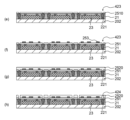
- FIG. 2 is a partially enlarged view of a region surrounded by a dashed line in FIG. 1; 1.
- the term “substantially” means that it includes a range that takes into account manufacturing tolerances, assembly variations, and the like, unless otherwise explicitly stated.
- the notation “X to Y” in the description of numerical ranges means X or more and Y or less, unless otherwise specified.
- “1 to 5% by mass” means “1% by mass or more and 5% by mass or less”.
- alkyl group includes not only alkyl groups without substituents (unsubstituted alkyl groups) but also alkyl groups with substituents (substituted alkyl groups).
- (meth)acryl used herein represents a concept that includes both acryl and methacryl. The same applies to similar notations such as "(meth)acrylate”.
- organic group as used herein means an atomic group obtained by removing one or more hydrogen atoms from an organic compound, unless otherwise specified.
- a "monovalent organic group” represents an atomic group obtained by removing one hydrogen atom from an arbitrary organic compound.
- electronic device refers to elements to which electronic engineering technology is applied, such as semiconductor chips, semiconductor elements, printed wiring boards, electric circuit display devices, information communication terminals, light-emitting diodes, physical batteries, and chemical batteries. , devices, final products, etc.
- the photosensitive resin composition of this embodiment contains a polyimide resin (A), a polyfunctional (meth)acrylate compound (B), a photosensitive agent (C), and a polymerization inhibitor (D).
- the polyimide resin (A) is a closed-ring polyimide resin containing a closed-ring imide structure represented by the following general formula (a).
- X is a divalent organic group and Y is a tetravalent organic group.
- polyamide/polyimide-based photosensitive resin compositions contain polyamide but do not contain polyimide before use (before forming a cured film). That is, conventionally, a photosensitive resin composition containing polyamide is used to form a film on a substrate, and the film is typically heated to ring-close the polyamide to form polyimide. However, in this case, the film shrinks due to the ring-closure reaction and the accompanying dehydration, and it is sometimes difficult to obtain a cured film with good flatness.
- the photosensitive resin composition of the present embodiment already contains the polyimide resin (A) before use (before forming the cured film).
- the polymerization reaction of the polyfunctional (meth)acrylate compound (B) is employed as the curing mechanism (this polymerization reaction does not involve dehydration in principle). From these matters, by forming a cured film using the photosensitive resin composition of the present embodiment, it is possible to form a cured film with small shrinkage due to heating and good flatness. In particular, it is possible to form a cured film with good flatness even on a substrate having steps.
- the photosensitive resin composition of the present embodiment it is easy to form a cured film having good heat resistance and good mechanical properties (for example, tensile elongation). Cured films in electronic devices are often required to have high heat resistance and good mechanical properties. Conventionally, however, when a resin is designed to be rigid in order to improve its heat resistance, the flexibility of the resin may be lost and mechanical properties such as elongation may be degraded. Although the details are unknown, in the photosensitive resin composition of the present embodiment, the polyfunctional (meth)acrylate compound (B) is intricately entangled with the polyimide resin (A) during curing (polymerization). , it is thought that a cured film different from conventional cured films is formed. This "entangled structure of polyimide resin and polyfunctional (meth)acrylate" is considered to be related to good heat resistance and good mechanical properties.
- the extensibility of the obtained photosensitive resin composition is improved as described above, but on the other hand, swelling of the cured portion and non-uniformity of the unexposed portion Inadequate dissolution (bridge) due to excessive dissolution, and phenomenon (foot) in which the unexposed area is not completely dissolved and remains may occur. Due to the occurrence of these defects, there is a possibility that a sufficient focus margin cannot be obtained.
- the photosensitizer (C) and the polymerization inhibitor (D) it was found that both good elongation and good focus margin can be achieved by using the photosensitizer (C) and the polymerization inhibitor (D).
- the curability of the exposed area is improved, and the generation of bridges in the development process can be suppressed while maintaining good mechanical properties. .
- the solubility of the unexposed area is improved, and the generation of feet in the development process is suppressed while maintaining good mechanical properties. can do.
- the focus margin of the photosensitive resin composition can be increased.
- the photosensitive agent (C) and the polymerization inhibitor (D) at the same time and highly controlling the ratio thereof, the cured film of the photosensitive resin composition of the present embodiment has good elongation. and a good focus margin can be achieved at the same time.
- the photosensitive resin composition of the present embodiment is preferably used for forming insulating layers in electronic devices or optical devices.
- the photosensitive resin composition of this embodiment contains a polyimide resin (A) containing a structural unit represented by general formula (a).
- X is a divalent organic group and Y is a tetravalent organic group.
- the photosensitive resin composition of the present embodiment tends to shrink less due to curing (heating) by using a polyimide resin containing a closed ring imide structure represented by the general formula (a) before curing.
- the number of moles of imide groups contained in the polyimide resin (A) is IM and the number of moles of amide groups contained in the polyimide resin (A) is AM, ⁇ IM/(IM+AM) ⁇ 100(%)
- the imidization ratio represented by is preferably 90% or more, more preferably 95% or more, and still more preferably 98% or more.
- the polyimide resin (A) is a resin having few or no ring-opening amide structures and many ring-closing imide structures.
- the imidization rate can be known, for example, from the area of the peak corresponding to the amide group or the area of the peak corresponding to the imide group in the NMR spectrum.
- the imidization rate can be known from the area of the peak corresponding to the amide group, the area of the peak corresponding to the imide group, and the like in the infrared absorption spectrum.
- the polyimide resin (A) preferably contains a polyimide resin containing a fluorine atom.
- the present inventors have found that polyimide resins containing fluorine atoms tend to have better solubility in organic solvents than polyimide resins containing no fluorine atoms. Therefore, by using a polyimide resin containing a fluorine atom, it is easy to make the property of the photosensitive resin composition varnish-like.
- the amount (mass ratio) of fluorine atoms in the polyimide resin containing fluorine atoms is, for example, 1 to 30% by mass, preferably 3 to 28% by mass, more preferably 5 to 25% by mass.
- a certain amount of fluorine atoms contained in the polyimide resin facilitates obtaining sufficient organic solvent solubility. On the other hand, from the viewpoint of balance with other performances, it is preferable that the amount of fluorine atoms is not too large.
- the mechanical properties (tensile elongation, etc.) of the cured product can be further improved.
- the polyimide resin (A) preferably has a group at its end that can react with an epoxy group to form a bond.
- groups include acid anhydride groups, hydroxy groups, amino groups, carboxy groups, and the like.
- the polyimide resin (A) has an acid anhydride group at its end.
- the acid anhydride group and the epoxy group are sufficiently easy to form a bond.
- the acid anhydride group is preferably a group having a cyclic acid anhydride skeleton.
- the "cyclic structure" herein is preferably a 5- or 6-membered ring, more preferably a 5-membered ring.
- X is a divalent organic group and Y is a tetravalent organic group.
- the divalent organic group of X and/or the tetravalent organic group of Y preferably contains an aromatic ring structure, more preferably a benzene ring structure. This tends to further increase the heat resistance.
- the divalent organic group of X and/or the tetravalent organic group of Y preferably has a structure in which 2 to 6 benzene rings are linked via a single bond or a divalent linking group.
- Examples of the divalent linking group here include an alkylene group, a fluorinated alkylene group, an ether group, and the like. Alkylene groups and fluorinated alkylene groups may be linear or branched.
- the number of carbon atoms in the divalent organic group of X is, for example, 6-30.
- the number of carbon atoms in the tetravalent organic group of Y is, for example, 6-20.
- Each of the two imide rings in general formula (a) is preferably a five-membered ring.
- the polyimide resin (A) preferably contains a polyimide resin containing a fluorine atom. This tends to increase the solubility in organic solvents. Moreover, from the viewpoint of further improving the organic solvent solubility, both X and Y are preferably fluorine atom-containing groups.
- the polyimide resin (A) more preferably contains a structural unit represented by the following general formula (aa).
- Y' represents a single bond or an alkylene group
- X has the same definition as X in formula (a).
- the alkylene group of Y' may be linear or branched. Some or all of the hydrogen atoms in the alkylene group of Y' are preferably substituted with fluorine atoms.
- the number of carbon atoms in the alkylene group of Y' is, for example, 1-6, preferably 1-4, more preferably 1-3.
- the polyimide resin (A) is typically prepared by (i) first reacting (condensation polymerization) a diamine and an acid dianhydride to synthesize a polyamide, and (ii) then imidating the polyamide (ring closure reacting), and (iii) introducing a desired functional group to the terminal of the polymer as necessary.
- Specific reaction conditions can be referred to Examples described later, the description of Patent Document 1 described above, and the like.
- the diamine is incorporated into the polymer as the divalent organic group X in general formula (a).
- the acid dianhydride is incorporated into the polymer as the tetravalent organic group Y in the general formula (a).
- one or two or more diamines can be used, and one or two or more acid dianhydrides can be used.
- Raw material diamines include, for example, 3,4′-diaminodiphenyl ether (3,4′-ODA), 4,4′-diamino-2,2′-bis(trifluoromethyl)biphenyl (TFMB), 3,3 ',5,5'-tetramethylbenzidine, 2,3,5,6-tetramethyl-1,4-phenylenediamine, 3,3'-diaminodiphenylsulfone, 3,3'dimethylbenzidine, 3,3'- Bis(trifluoromethyl)benzidine, 2,2'-bis(p-aminophenyl)hexafluoropropane, bis(trifluoromethoxy)benzidine (TFMOB), 2,2'-bis(pentafluoroethoxy)benzidine (TFEOB) , 2,2′-trifluoromethyl-4,4′-oxydianiline (OBABTF), 2-phenyl-2-trifluoromethyl-bis(p-aminophenyl)
- acid dianhydrides used as raw materials include pyromellitic anhydride (PMDA), diphenyl ether-3,3′,4,4′-tetracarboxylic dianhydride (ODPA), benzophenone-3,3′, 4,4'-tetracarboxylic dianhydride (BTDA), biphenyl-3,3',4,4'-tetracarboxylic dianhydride (BPDA), diphenylsulfone-3,3',4,4'- Tetracarboxylic dianhydride (DSDA), diphenylmethane-3,3',4,4'-tetracarboxylic dianhydride, 2,2-bis(3,4-phthalic anhydride) propane, 2,2-bis (3,4-Phthalic anhydride)-1,1,1,3,3,3-hexafluoropropane (6FDA) and the like can be mentioned.
- acid dianhydrides that can be used are not limited to these.
- the usage ratio of the diamine and the acid dianhydride is basically 1:1 in terms of molar ratio. However, one may be used in excess to obtain the desired terminal structure. Specifically, by using an excessive amount of diamine, the ends (both ends) of the polyimide resin (A) tend to become amino groups. On the other hand, when the acid dianhydride is excessively used, the ends (both ends) of the polyimide resin (A) tend to become acid anhydride groups. As described above, in the present embodiment, the polyimide resin (A) preferably has an acid anhydride group at its terminal. Therefore, in the present embodiment, it is preferable to use an excess amount of acid dianhydride when synthesizing the polyimide resin (A).
- terminal amino groups and/or acid anhydride groups of the polyimide obtained by condensation polymerization may be reacted with some kind of reagent so that the polyimide terminals have desired functional groups.
- the weight average molecular weight of the polyimide resin (A) is, for example, 5,000 to 100,000, preferably 7,000 to 75,000, more preferably 10,000 to 50,000.
- the weight average molecular weight of the polyimide resin (A) is large to some extent, for example, sufficient heat resistance of the cured film can be obtained.
- the weight average molecular weight of the polyimide resin (A) is not too large, it becomes easier to dissolve the polyimide resin (A) in the organic solvent.
- the weight average molecular weight can usually be determined by gel permeation chromatography (GPC) using polystyrene as a standard substance.
- the photosensitive resin composition of this embodiment contains a polyfunctional (meth)acrylate compound (B).
- a polyfunctional (meth)acrylate compound (B) those having two or more (meth)acryloyl groups in one molecule can be mentioned without particular limitation.
- the polyfunctional (meth)acrylate compound (B) is preferably trifunctional or higher.
- the upper limit for the number of functional groups is, for example, 11 functional groups in consideration of the availability of raw materials.
- the polyfunctional (meth)acrylate compound (B) having a large number of functional groups ((meth)acryloyl groups) is used, the chemical resistance of the cured film tends to increase.
- the polyfunctional (meth)acrylate compound (B) having a small number of functional groups ((meth)acryloyl groups) is used, mechanical properties such as tensile elongation of the cured film tend to be improved.
- the polyfunctional (meth)acrylate compound (B) preferably contains a 3- to 4-functional (meth)acrylate compound (B1).
- the polyfunctional (meth)acrylate compound (B) preferably contains a pentafunctional or higher (meth)acrylate compound (B2).
- the polyfunctional (meth)acrylate compound (B) can contain a compound represented by the following general formula (b).
- R' is a hydrogen atom or a methyl group
- n is 0 to 3
- R is a hydrogen atom or a (meth)acryloyl group.
- polyfunctional (meth)acrylate compound (B) examples include the following. Of course, polyfunctional (meth)acrylate compounds (B) are not limited to these.
- Aronix M-400, Aronix M-460, Aronix M-402, Aronix M-510, Aronix M-520 (manufactured by Toagosei Co., Ltd.), KAYARAD T-1420, KAYARAD DPHA, KAYARAD DPCA20, KAYARAD DPCA30, KAYARAD DPCA60, KAYARAD DPCA120 (manufactured by Nippon Kayaku Co., Ltd.), Viscoat #230, Viscoat #300, Viscoat #802, Viscoat #2500, Viscoat #1000, Viscoat #1080 (manufactured by Osaka Organic Chemical Industry Co., Ltd.), NK Ester A-BPE-10 , NK Ester A-GLY-9E, NK Ester A-9550, and NK Ester A-DPH (manufactured by Shin-Nakamura Chemical Co., Ltd.).
- the photosensitive resin composition may contain only one polyfunctional (meth)acrylate compound (B), or may contain two or more polyfunctional (meth)acrylate compounds (B). In the latter case, it is preferable to use together a polyfunctional (meth)acrylate compound (B) having a different number of functional groups.
- polyfunctional (meth)acrylate compounds (B) with different numbers of functional groups together, a more complex "entangled structure of polyimide and polyfunctional (meth)acrylate" can be created, resulting in better heat resistance and mechanical properties. It is considered possible.
- the amount of the polyfunctional (meth)acrylate compound (B) with respect to 100 parts by mass of the polyimide resin (A) is, for example, 25 to 150 parts by mass, preferably 50 to 120 parts by mass, more preferably 70 to 100 parts by mass, more preferably 80 to 95 parts by mass.
- the amount of the polyfunctional (meth)acrylate compound (B) used is not particularly limited, but one or more of the various properties can be enhanced by appropriately adjusting the amount used as described above.
- the entangled structure of the polyimide having a cyclic structure and the polyfunctional (meth)acrylate is formed by curing, but the polyimide resin (A By appropriately adjusting the amount of the polyfunctional (meth) acrylate compound (B) for ), the polyimide resin (A) and the polyfunctional (meth) acrylate compound (B) are sufficiently entangled, and are not involved in the entanglement. It is believed that there are fewer redundant components, resulting in better performance.
- the photosensitive resin composition of this embodiment contains a photosensitive agent (C).
- the photosensitive agent (C) is not particularly limited as long as it can generate active species by light and cure the photosensitive resin composition.
- the photosensitizer (C) preferably contains a photoradical generator.
- a photoradical generator is particularly effective for polymerizing the polyfunctional (meth)acrylate compound (B).
- the photoradical generator that can be used is not particularly limited, and known ones can be used as appropriate.
- the photosensitive resin composition may contain only 1 type of photosensitive agents (C), and may contain 2 or more types.
- the content of the photosensitive agent (C) is, for example, 5 parts by mass or more and 30 parts by mass or less, preferably 10 parts by mass or more and 25 parts by mass or less with respect to 100 parts by mass of the polyimide resin (A).
- the photosensitive resin composition of this embodiment contains a polymerization inhibitor (D).
- the polymerization inhibitor (D) includes, for example, hindered phenol compounds, hindered amine compounds, N-oxyl compounds and thioether compounds.
- hindered phenol compounds, hindered amine-based compounds, and N-oxyl compounds are preferably included from the viewpoint of improving the solubility of unexposed areas.
- hindered phenol compounds include 1,3,5-tris(3,5-di-tert-butyl-4-hydroxybenzyl)-1,3,5-triazine-2,4,6(1H, 3H,5H)-trione, 4,4′,4′′-(1-methylpropanyl-3-ylidene)tris(6-tert-butyl-m-cresol), 6,6′-di-tert-butyl- 4,4′-butylidenedi-m-cresol, pentaerythritol tetrakis[3-(3,5-di-tert-butyl-4-hydroxyphenyl)propionate] (Irganox 1010), 3,9-bis ⁇ 2-[3- (3-tert-butyl-4-hydroxy-5-methylphenyl)propionyloxy]-1,1-dimethylethyl ⁇ -2,4,8,10-tetraoxaspiro[5.5]undecane, 1,3, 5-tris(3,
- hindered amine compounds include tetrakis(1,2,2,6,6-pentamethyl-4-piperidyl)butane-1,2,3,4-tetracarboxylate, tetrakis(2,2,6,6- Tetramethyl-4-piperidyl)butane-1,2,3,4-tetracarboxylate, 1,2,3,4-butanetetracarboxylic acid and 1,2,2,6,6-pentamethyl-4-piperidinol and 3,9-bis(2-hydroxy-1,1-dimethylethyl)-2,4,8,10-tetraoxaspiro[5.5]undecane mixed ester, 1,2,3,4-butane Tetracarboxylic acid with 2,2,6,6-tetramethyl-4-piperidinol and 3,9-bis(2-hydroxy-1,1-dimethylethyl)-2,4,8,10-tetraoxaspiro[5 .5] mixed esters with undecane, bis(1,2,2,6,6
- N-oxyl compounds include 4-benzoyloxy-2,2,6,6-tetramethylpiperidinooxyl (4-benzoyloxy TEMPO), N-nitrosodiphenylamine, N-nitroso-N-phenylhydroxylamine. , 2,2,6,6-tetramethylpiperidine-1-oxyl (TEMPO), 4-hydroxy-2,2,6,6-tetramethylpiperidi-1-oxyl free radical (4-hydroxy TEMPO), sebacin acid bis(2,2,6,6-tetramethyl-4-piperidyl-1-oxyl) (bis sebacate TEMPO); These may be used individually by 1 type, or may use 2 or more types together.
- TEMPO 2,2,6,6-tetramethylpiperidine-1-oxyl
- 4-hydroxy-2,2,6,6-tetramethylpiperidi-1-oxyl free radical (4-hydroxy TEMPO)
- sebacin acid bis(2,2,6,6-tetramethyl-4-piperidyl-1-oxyl) bis sebacate TEMPO
- the thioether compounds include 2,2-bis ⁇ [3-(dodecylthio)-1-oxopropoxy]methyl ⁇ propane-1,3-diylbis[3-(dodecylthio)propionate], di(tridecyl)-3 , 3′-thiodipropionate and the like. These may be used individually by 1 type, or may use 2 or more types together.
- the content of the polymerization inhibitor (D) with respect to 100 parts by mass of the polyimide resin (A) is preferably 0.1 parts by mass or more and 5 parts by mass or less, more preferably 1 It is at least 3 parts by mass and no more than 3 parts by mass. If the content of the polymerization inhibitor (D) is within the above range, the solubility of the unexposed area is improved, and the phenomenon that the unexposed area in the development process is not completely dissolved and remains while maintaining good mechanical properties (foot ) can be suppressed.
- the content of the polymerization inhibitor (D) with respect to 100 parts by mass of the photosensitive agent (C) is preferably 1 part by mass or more and 30 parts by mass or less, more preferably 5 parts by mass. It is more than 20 parts by mass and less than 20 parts by mass. If the content of the polymerization inhibitor (D) with respect to 100 parts by mass of the photosensitive agent (C) is within the above range, the cured film of the photosensitive resin composition of the present embodiment has good elongation and a good focus margin. It is possible to achieve both.
- the photosensitive resin composition of the present embodiment preferably contains a thermal radical generator (E).
- a thermal radical generator E
- the thermal radical generator (E) for example, the heat resistance of the cured film can be further enhanced and/or the chemical resistance (resistance to organic solvents and the like) of the cured film can be enhanced. This is probably because the use of the thermal radical generator (E) further accelerates the polymerization reaction of the polyfunctional (meth)acrylate compound (B).
- the thermal radical generator (E) preferably contains an organic peroxide.
- Organic peroxides include octanoyl peroxide, lauroyl peroxide, stearoyl peroxide, 1,1,3,3-tetramethylbutylperoxy 2-ethylhexanoate, oxalic acid peroxide, 2,5-dimethyl- 2,5-di(2-ethylhexanoylperoxy)hexane, 1-cyclohexyl-1-methylethylperoxy 2-ethylhexanoate, t-hexylperoxy 2-ethylhexanoate, t-butylperoxy 2-ethylhexanoate, m-toluyl peroxide, benzoyl peroxide, benzoyl peroxide, methyl ethyl ketone peroxide, acetyl peroxide, t-butyl hydroperoxide, di-t-buty
- thermal radical generator (E) When the thermal radical generator (E) is used, only one thermal radical generator (E) may be used, or two or more thermal radical generators (E) may be used. When the thermal radical generator (E) is used, the amount thereof is preferably 0.1 parts by mass or more and 30 parts by mass or less, more preferably 1 part by mass or more and 20 parts by mass, relative to 100 parts by mass of the polyimide resin (A). It is below.
- the photosensitive resin composition of the present embodiment preferably contains a cross-linking agent (F).
- a cross-linking agent (F) By using the cross-linking agent (F), for example, the cross-linking agent (F) reacts with other components contained in the photosensitive resin composition, or the cross-linking agent (F) is polymerized with each other, and the cross-linking agent (F) becomes closely entangled with the photosensitive resin composition. This is thought to improve the chemical resistance and elongation of the resin film made of the cured product of the photosensitive resin composition.
- the cross-linking agent (F) preferably has one epoxy-containing group at one end of the molecule and one (meth)acryloyl group at the other end of the molecule.
- the "epoxy-containing group” refers to a substituent having a three-membered ether oxacyclopropane (oxirane) in its structural formula.
- oxirane a substituent having a three-membered ether oxacyclopropane (oxirane) in its structural formula.
- Specific examples thereof include an epoxy group, a glycidyl group, a glycidyl ether group, and one or more hydrogen atoms in an organic group to an epoxy group, a glycidyl group, or a glycidyl ether group (a group obtained by removing hydrogen from the OH group of glycidol).
- Substituted groups may be mentioned, and specific examples include 1,2-epoxycyclohexyl group and the like.
- organic group is not particularly limited, examples include methyl group, ethyl group, n-propyl group, isopropyl group, n-butyl group, isobutyl group, sec-butyl group, tert-butyl group, pentyl group, neopentyl group and hexyl.
- alkyl groups such as group, heptyl group, octyl group, nonyl group and decyl group; alkenyl groups such as allyl group, pentenyl group and vinyl group; alkynyl groups such as ethynyl group; alkylidene groups such as methylidene group and ethylidene group; aryl groups such as , naphthyl and anthracenyl groups; aralkyl groups such as benzyl and phenethyl groups; alkaryl groups such as tolyl and xylyl groups; or cycloalkyl groups such as adamantyl, cyclopentyl, cyclohexyl and cyclooctyl groups is mentioned.
- the cross-linking agent (F) preferably contains a compound represented by general formula (1).
- X 1 represents a (meth)acryloyl group.
- X2 represents a glycidyl group, a glycidyl ether group, an epoxy group or a 1,2-epoxycyclohexyl group as an epoxy-containing group.
- n represents an integer of 1-10.
- the reactivity between the cross-linking agent (F) and other components contained in the photosensitive resin composition or the cross-linking agent (F) is improved, and the photosensitive resin composition It is preferable because the chemical resistance and elongation of the resin film made of the cured product are improved.
- n is within the range of 1 to 10, the elongation rate of the resin film made of the cured product of the photosensitive resin composition becomes more suitable, which is preferable.
- the cross-linking agent (F) it is preferable that one or more compounds selected from compounds represented by any one of the following chemical formulas (2) to (4) be included as the compound satisfying the general formula (1).
- the chemical resistance and elongation of the resin film made of the cured product of the photosensitive resin composition are increased. You can have both in balance.
- the content of the cross-linking agent (F) is, for example, 0.1 parts by mass or more, preferably 0.5 parts by mass or more, more preferably 1 part by mass or more with respect to 100 parts by mass of the polyimide resin (A). .
- the content of the cross-linking agent (F) is 0.1 parts by mass or more, the cured product of the photosensitive resin composition can have high chemical resistance.
- the content of the cross-linking agent (F) is, for example, 30 parts by mass or less, preferably 20 parts by mass or less, more preferably 10 parts by mass or less, relative to 100 parts by mass of the polyimide resin (A).
- the content of the cross-linking agent (F) is 30 parts by mass or less, the ratio of the polyimide resin (A) in the photosensitive resin composition is maintained, and the elongation of the cured product of the photosensitive resin composition becomes good. In addition, the adhesion between the photosensitive resin composition and the substrate is sufficiently improved.
- the photosensitive resin composition of the present embodiment may contain only one type of cross-linking agent (F), or may contain two or more types.
- the photosensitive resin composition of this embodiment preferably contains a silane coupling agent (G).
- a silane coupling agent (G) for example, the adhesion between the substrate and the cured film can be further enhanced.
- silane coupling agent (G) examples include amino group-containing silane coupling agents, epoxy group-containing silane coupling agents, (meth)acryloyl group-containing silane coupling agents, mercapto group-containing silane coupling agents, vinyl group-containing Silane coupling agents such as silane coupling agents, ureido group-containing silane coupling agents, sulfide group-containing silane coupling agents, and silane coupling agents having a cyclic anhydride structure can be used.
- amino group-containing silane coupling agents include bis(2-hydroxyethyl)-3-aminopropyltriethoxysilane, ⁇ -aminopropyltriethoxysilane, ⁇ -aminopropyltrimethoxysilane, ⁇ -aminopropylmethyldiethoxysilane.
- Silane ⁇ -aminopropylmethyldimethoxysilane, N- ⁇ (aminoethyl) ⁇ -aminopropyltrimethoxysilane, N- ⁇ (aminoethyl) ⁇ -aminopropyltriethoxysilane, N- ⁇ (aminoethyl) ⁇ -amino Propylmethyldimethoxysilane, N- ⁇ (aminoethyl) ⁇ -aminopropylmethyldiethoxysilane, N-phenyl- ⁇ -amino-propyltrimethoxysilane and the like.
- epoxy group-containing silane coupling agents include ⁇ -glycidoxypropyltrimethoxysilane, ⁇ -glycidoxypropylmethyldiethoxysilane, ⁇ -(3,4-epoxycyclohexyl)ethyltrimethoxysilane, and ⁇ -glycidyl. propyltrimethoxysilane and the like.
- Examples of (meth)acryloyl group-containing silane coupling agents include ⁇ -((meth)acryloyloxypropyl)trimethoxysilane, ⁇ -((meth)acryloyloxypropyl)methyldimethoxysilane, ⁇ -((meth) acryloyloxypropyl)methyldiethoxysilane and the like.
- Mercapto group-containing silane coupling agents include, for example, 3-mercaptopropyltrimethoxysilane.
- Vinyl group-containing silane coupling agents include, for example, vinyltris( ⁇ -methoxyethoxy)silane, vinyltriethoxysilane, vinyltrimethoxysilane and the like.
- Ureido group-containing silane coupling agents include, for example, 3-ureidopropyltriethoxysilane.
- sulfide group-containing silane coupling agents include bis(3-(triethoxysilyl)propyl)disulfide and bis(3-(triethoxysilyl)propyl)tetrasulfide.
- Silane coupling agents having a cyclic anhydride structure include, for example, 3-trimethoxysilylpropylsuccinic anhydride, 3-triethoxysilylpropylsuccinic anhydride, and 3-dimethylmethoxysilylpropylsuccinic anhydride. be done.
- a silane coupling agent having a cyclic anhydride structure is particularly preferably used.
- the details are unknown, it is presumed that the cyclic anhydride structure readily reacts with the main chain, side chains and/or terminals of the polyimide resin (A), resulting in a particularly good effect of improving adhesion.
- the silane coupling agent (G) When the silane coupling agent (G) is used, it may be used alone, or two or more adhesion aids may be used in combination.
- the amount used is, for example, 0.1 to 20 parts by mass, preferably 0.3 to 15 parts by mass when the amount of polyimide resin (A) used is 100 parts by mass. parts, more preferably 0.4 to 12 parts by mass, and still more preferably 0.5 to 10 parts by mass.
- the photosensitive resin composition of the present embodiment preferably contains a curing catalyst (H).
- This curing catalyst (H) functions to accelerate the reaction of the cross-linking agent (F).
- the reaction involving the cross-linking agent (F) can proceed sufficiently, and for example, the tensile elongation of the cured film can be further improved.
- the curing catalyst (H) includes compounds known as curing catalysts for epoxy resins (often called curing accelerators). For example, diazabicycloalkenes such as 1,8-diazabicyclo[5,4,0]undecene-7 and derivatives thereof; amine compounds such as tributylamine and benzyldimethylamine; imidazole compounds such as 2-methylimidazole; triphenyl Organic phosphines such as phosphine and methyldiphenylphosphine; tetra-substituted phosphonium salts such as phosphonium/tetranaphthyloxyborate and tetraphenylphosphonium/4,4'-sulfonyldiphenolate; and triphenylphosphine obtained by adducting benzoquinone. Among them, organic phosphines are preferred.
- the curing catalyst (H) When the curing catalyst (H) is used, its amount is, for example, 1 to 80 parts by mass, preferably 2 to 50 parts by mass, more preferably 3 to 30 parts by mass with respect to 100 parts by mass of the cross-linking agent (F). .
- the photosensitive resin composition of the present embodiment preferably contains surfactant (I). This can further improve the applicability of the photosensitive resin composition and the flatness of the film.
- Surfactants (I) include fluorine-based surfactants, silicone-based surfactants, alkyl-based surfactants, and acrylic surfactants. From another point of view, the surfactant is preferably nonionic. The use of nonionic surfactants is preferable, for example, from the viewpoint of suppressing unintentional reactions with other components in the composition and enhancing the storage stability of the composition.
- Surfactant (I) preferably contains a surfactant containing at least one of a fluorine atom and a silicon atom. This contributes to obtaining a uniform resin film (improvement of coatability), improvement of developability, and improvement of adhesive strength.
- a surfactant is preferably, for example, a nonionic surfactant containing at least one of a fluorine atom and a silicon atom.
- Examples of commercially available products that can be used as the surfactant (I) include F-251, F-253, F-281, F-430, F-477, and F-251, F-253, F-281, F-430, F-477, and F-251, F-253, F-281, F-430, and F-477, manufactured by DIC Corporation.
- Fluorine-containing oligomer structure surfactants such as, fluorine-containing nonionic surfactants such as Ftergent 250 and Ftergent 251 manufactured by Neos Co., Ltd., SILFOAM (registered trademark) series manufactured by Wacker Chemie (for example, and silicone surfactants such as SD 100 TS, SD 670, SD 850, SD 860, SD 882).
- FC4430 and FC4432 manufactured by 3M are also preferable surfactants.
- the photosensitive resin composition of the present embodiment contains surfactant (I), it can contain one or more surfactants.
- the photosensitive resin composition of the present embodiment contains the surfactant (I)
- the amount thereof is, when the content of the polyimide resin (A) is 100 parts by mass, for example 0.001 to 1 part by mass, preferably is 0.005 to 0.5 parts by mass.
- the photosensitive resin composition of this embodiment preferably contains a solvent (J). Thereby, a photosensitive resin film can be easily formed on a substrate (particularly, a substrate having a step) by a coating method.
- Solvent (J) usually contains an organic solvent.
- the organic solvent is not particularly limited as long as it can dissolve or disperse each component described above and does not substantially chemically react with each component.
- organic solvents include acetone, methyl ethyl ketone, toluene, propylene glycol methyl ethyl ether, propylene glycol dimethyl ether, propylene glycol 1-monomethyl ether 2-acetate, diethylene glycol ethyl methyl ether, diethylene glycol monoethyl ether acetate, diethylene glycol monobutyl ether acetate, benzyl Alcohol, propylene carbonate, ethylene glycol diacetate, propylene glycol diacetate, propylene glycol monomethyl ether acetate, dipropylene glycol methyl-n-propyl ether, butyl acetate, ⁇ -butyrolactone, methyl lactate, ethyl lactate, butyl lactate and the like. . These may be used singly or in combination.
- the photosensitive resin composition of the present embodiment contains the solvent (J)
- the photosensitive resin composition of the present embodiment is usually in the form of varnish.
- the photosensitive resin composition of the present embodiment is preferably a varnish-like composition in which at least the polyimide resin (A) and the polyfunctional (meth)acrylate compound (B) are dissolved in the solvent (J). composition. Since the photosensitive resin composition of the present embodiment is in the form of varnish, it is possible to form a uniform film by coating. Further, since the polyimide resin (A) and the polyfunctional (meth)acrylate compound (B) are "dissolved” in the solvent (J), a homogeneous cured film can be obtained.
- the concentration of the total solid content (nonvolatile components) in the photosensitive resin composition is preferably 10 to 50% by mass, more preferably 20 to 45% by mass.
- concentration of the total solid content (nonvolatile components) in the photosensitive resin composition is preferably 10 to 50% by mass, more preferably 20 to 45% by mass.
- each component can fully be melt
- good coatability can be ensured, which in turn leads to improvement in flatness during spin coating.
- the viscosity of the photosensitive resin composition can be appropriately controlled by adjusting the content of the non-volatile component.
- the ratio of the polyimide resin (A) and the polyfunctional (meth)acrylate compound (B) in the entire composition is preferably 20 to 50% by mass.
- the photosensitive resin composition of the present embodiment may contain components other than the components listed above, if necessary.
- Such components include, for example, water, fillers such as silica, sensitizers, film-forming agents, and the like.
- the method for manufacturing an electronic device includes: A film forming step of forming a photosensitive resin film on a substrate using the photosensitive resin composition described above; an exposure step of exposing the photosensitive resin film; a developing step of developing the exposed photosensitive resin film; including. Moreover, it is preferable that the method for manufacturing an electronic device of the present embodiment includes a thermosetting step of heating and curing the exposed photosensitive resin film after the above-described developing step. Thereby, a cured film having sufficient heat resistance can be obtained. As described above, an electronic device provided with a cured film of the photosensitive resin composition of the present embodiment can be manufactured.
- FIG. 1 is a longitudinal sectional view showing an example of the electronic device of this embodiment.
- FIG. 2 is a partially enlarged view of a region surrounded by a dashed line in FIG.
- the upper side in FIG. 1 is called “upper”
- the lower side is called “lower”.
- the electronic device 1 shown in FIG. 1 has a so-called package-on-package structure including a through electrode substrate 2 and a semiconductor package 3 mounted thereon.
- the through electrode substrate 2 includes an insulating layer 21 , a plurality of through wirings 221 penetrating from the upper surface to the lower surface of the insulating layer 21 , a semiconductor chip 23 embedded inside the insulating layer 21 , and provided on the lower surface of the insulating layer 21 . an upper wiring layer 25 provided on the upper surface of the insulating layer 21; and solder bumps 26 provided on the lower surface of the lower wiring layer 24. As shown in FIG.
- the semiconductor package 3 includes a package substrate 31, a semiconductor chip 32 mounted on the package substrate 31, bonding wires 33 electrically connecting the semiconductor chip 32 and the package substrate 31, and the semiconductor chip 32 and the bonding wires 33. It has an embedded sealing layer 34 and solder bumps 35 provided on the lower surface of the package substrate 31 .
- a semiconductor package 3 is laminated on the through electrode substrate 2 . Thereby, the solder bumps 35 of the semiconductor package 3 and the upper wiring layers 25 of the through electrode substrate 2 are electrically connected.
- the through electrode substrate 2 and the semiconductor package 3 having different semiconductor chips are stacked, the mounting density per unit area can be increased. Therefore, it is possible to achieve both miniaturization and high performance.
- the through electrode substrate 2 and the semiconductor package 3 will be further detailed below.
- the lower wiring layer 24 and the upper wiring layer 25 provided in the through electrode substrate 2 shown in FIG. 2 each include an insulating layer, a wiring layer, a through wiring, and the like.
- the lower wiring layer 24 and the upper wiring layer 25 include wiring inside and on the surface, and are electrically connected to each other through the through wiring 221 penetrating the insulating layer 21 .
- a wiring layer included in the lower wiring layer 24 is connected to the semiconductor chip 23 and the solder bumps 26 . Therefore, the lower wiring layer 24 functions as a rewiring layer for the semiconductor chip 23 and the solder bumps 26 function as external terminals of the semiconductor chip 23 .
- the through wiring 221 shown in FIG. 2 is provided so as to penetrate the insulating layer 21 as described above. As a result, the lower wiring layer 24 and the upper wiring layer 25 are electrically connected, and the through electrode substrate 2 and the semiconductor package 3 can be stacked. can.
- a cured film of the photosensitive resin composition of the present embodiment can be used to form the insulating layer of the rewiring layer.
- the semiconductor chip 23 and the rewiring layer (upper wiring layer 25) provided on the surface of the semiconductor chip 23 are provided, and the insulating layer in the rewiring layer is the photosensitive layer of this embodiment. It is possible to realize an electronic device composed of a cured product of a flexible resin composition.
- the effect of reinforcing the insulating layer 21 is obtained because the through wiring 221 penetrates the insulating layer 21 . Therefore, even when the mechanical strength of the lower wiring layer 24 and the upper wiring layer 25 is low, the mechanical strength of the entire through electrode substrate 2 can be prevented from being lowered. As a result, the thickness of the lower wiring layer 24 and the upper wiring layer 25 can be further reduced, and the height of the electronic device 1 can be further reduced.
- the electronic device 1 shown in FIG. 1 also includes a through wire 222 provided so as to penetrate the insulating layer 21 located on the upper surface of the semiconductor chip 23 in addition to the through wire 221 . Thereby, electrical connection between the upper surface of the semiconductor chip 23 and the upper wiring layer 25 can be achieved.
- the insulating layer 21 is provided so as to cover the semiconductor chip 23 . This enhances the effect of protecting the semiconductor chip 23 . As a result, the reliability of the electronic device 1 can be improved. Also, the electronic device 1 can be easily applied to a mounting system such as the package-on-package structure according to the present embodiment.
- the diameter W (see FIG. 2) of the through wiring 221 is not particularly limited, but is preferably about 1 to 100 ⁇ m, more preferably about 2 to 80 ⁇ m. Thereby, the electrical conductivity of the through wiring 221 can be ensured without impairing the mechanical properties of the insulating layer 21 .
- the semiconductor package 3 shown in FIG. 1 may be any form of package.
- QFP Quad Flat Package
- SOP Small Outline Package
- BGA Bit Grid Array
- CSP Chip Size Package
- QFN Quadrature Package
- SON Small Outline Package
- Forms such as LF-BGA (Lead Flame BGA) can be mentioned.
- the arrangement of the semiconductor chips 32 is not particularly limited, as an example in FIG. 1, a plurality of semiconductor chips 32 are stacked. As a result, the mounting density is increased.
- the plurality of semiconductor chips 32 may be arranged side by side in the planar direction, or may be arranged side by side in the planar direction while being stacked in the thickness direction.
- the package substrate 31 may be any substrate, but is, for example, a substrate that includes an insulating layer, a wiring layer, a through wiring, etc. (not shown). Among them, the solder bump 35 and the bonding wire 33 can be electrically connected via the through wiring.
- the sealing layer 34 is made of, for example, a known sealing resin material. By providing such a sealing layer 34, the semiconductor chip 32 and the bonding wires 33 can be protected from external forces and the external environment.
- the semiconductor chip 23 provided in the through electrode substrate 2 and the semiconductor chip 32 provided in the semiconductor package 3 are arranged close to each other.
- one of the semiconductor chip 23 and the semiconductor chip 32 is a CPU (Central Processing Unit), a GPU (Graphics Processing Unit), an AP (Application Processor) or other computing element, and the other is a DRAM (Dynamic Random Access). Memory), flash memory, or the like, these elements can be arranged close to each other in the same device. This makes it possible to realize the electronic device 1 that achieves both high functionality and miniaturization.
- FIG. 3 is a process drawing showing a method of manufacturing the electronic device 1 shown in FIG. 4 to 6 are diagrams for explaining a method of manufacturing the electronic device 1 shown in FIG. 1, respectively.
- the method of manufacturing the electronic device 1 includes a chip placement step S1 for obtaining an insulating layer 21 so as to embed a semiconductor chip 23 and through wirings 221 and 222 provided on a substrate 202, and an upper layer on the insulating layer 21 and on the semiconductor chip 23.
- An upper wiring layer forming step S2 for forming the wiring layer 25 a substrate peeling step S3 for peeling the substrate 202, a lower wiring layer forming step S4 for forming the lower wiring layer 24, a solder bump 26 is formed, and a through electrode substrate is formed.
- 2 and a stacking step S6 of stacking the semiconductor package 3 on the through electrode substrate 2 is a stacking step S6 of stacking the semiconductor package 3 on the through electrode substrate 2 .
- the photosensitive resin varnish 5 (a varnish-like photosensitive resin composition) is placed on the insulating layer 21 and the semiconductor chip 23 to form a photosensitive resin layer 2510.
- a second curing step S28 and a through-wiring forming step S29 of forming the through-wiring 254 in the opening 424 (through-hole) are included.
- Chip placement step S1 First, as shown in FIG. 4A, a chip including a substrate 202, a semiconductor chip 23 and through wirings 221 and 222 provided on the substrate 202, and an insulating layer 21 provided so as to bury them An embedded structure 27 is prepared.
- the constituent material of the substrate 202 is not particularly limited, but examples include metal materials, glass materials, ceramic materials, semiconductor materials, organic materials, and the like. Also, the substrate 202 may be a semiconductor wafer such as a silicon wafer, a glass wafer, or the like.
- the semiconductor chip 23 is adhered onto the substrate 202 .
- a plurality of semiconductor chips 23 are arranged side by side on the same substrate 202 while being separated from each other.
- the plurality of semiconductor chips 23 may be of the same type, or may be of different types.
- the substrate 202 and the semiconductor chip 23 may be fixed via an adhesive layer (not shown) such as a die attach film.
- An interposer (not shown) may be provided between the substrate 202 and the semiconductor chip 23 as required.
- the interposer functions as a rewiring layer of the semiconductor chip 23, for example. Therefore, the interposer may have pads (not shown) for electrical connection with electrodes of the semiconductor chip 23, which will be described later. As a result, the pad spacing and arrangement pattern of the semiconductor chip 23 can be changed, and the degree of freedom in designing the electronic device 1 can be further enhanced.
- an inorganic substrate such as a silicon substrate, a ceramic substrate, or a glass substrate, an organic substrate such as a resin substrate, or the like is used.
- the insulating layer 21 may be, for example, a resin film (organic insulating layer) containing a thermosetting resin or a thermoplastic resin such as those listed as components of the photosensitive resin composition, and may be an ordinary sealing layer used in the technical field of semiconductors. It may be a stopping material.
- Examples of materials constituting the through-wirings 221 and 222 include copper or copper alloys, aluminum or aluminum alloys, gold or gold alloys, silver or silver alloys, nickel or nickel alloys, and the like.
- a chip-embedded structure 27 manufactured by a method different from the above may be prepared.
- the application of the photosensitive resin varnish 5 is performed using, for example, a spin coater, a bar coater, a spray device, an inkjet device, or the like.
- the viscosity of the photosensitive resin varnish 5 is not particularly limited, but is 10 cP to 6000 cP, preferably 20 cP to 5000 cP, more preferably 30 cP to 4000 cP.
- a thinner photosensitive resin layer 2510 (see FIG. 4D) can be formed.
- the upper wiring layer 25 can be made thinner, and the thickness of the electronic device 1 can be easily reduced.
- the viscosity of the photosensitive resin varnish 5 is, for example, a value measured using a cone-plate viscometer (TV-25, manufactured by Toki Sangyo Co., Ltd.) at a rotation speed of 100 rpm.
- the conditions for drying the photosensitive resin varnish 5 are not particularly limited, but include, for example, heating at a temperature of 80 to 150° C. for 1 to 60 minutes.
- the photosensitive resin film is the photosensitive resin composition of the present embodiment and is a resin film having photosensitivity.
- a photosensitive resin film is manufactured by applying, for example, a photosensitive resin varnish 5 onto a substrate such as a carrier film using various coating devices, and then drying the resulting coating film.
- the photosensitive resin layer 2510 is subjected to pre-exposure heat treatment as necessary.
- pre-exposure heat treatment the molecules contained in the photosensitive resin layer 2510 are stabilized, and the reaction in the first exposure step S21 described later can be stabilized.
- by heating under the heating conditions described later adverse effects on the photoacid generator due to heating can be minimized.
- the temperature of the pre-exposure heat treatment is preferably 70 to 130°C, more preferably 75 to 120°C, still more preferably 80 to 110°C. If the temperature of the pre-exposure heat treatment is lower than the lower limit, there is a risk that the pre-exposure heat treatment may fail to achieve the purpose of stabilizing molecules. On the other hand, if the temperature of the pre-exposure heat treatment exceeds the upper limit, the movement of the photo-acid generator becomes too active, and the influence that acid is less likely to be generated even when light is irradiated in the first exposure step S21 described later. becomes wider, and the processing precision of patterning may deteriorate.
- the time of the pre-exposure heat treatment is appropriately set according to the temperature of the pre-exposure heat treatment. 6 minutes. If the pre-exposure heat treatment time is less than the lower limit, the heating time will be insufficient, so there is a risk that the pre-exposure heat treatment will fail to achieve the purpose of stabilizing molecules. On the other hand, if the pre-exposure heat treatment time exceeds the above upper limit, the heating time is too long, and even if the pre-exposure heat treatment temperature is within the above range, the action of the photoacid generator is inhibited. There is a risk that it will be lost.
- the atmosphere of the heat treatment is not particularly limited. Although an inert gas atmosphere, a reducing gas atmosphere, or the like may be used, the atmosphere is selected in consideration of work efficiency and the like.
- the atmospheric pressure is not particularly limited. It may be under reduced pressure or under increased pressure, but considering work efficiency, etc., normal pressure is used.
- the normal pressure means a pressure of about 30 to 150 kPa, preferably atmospheric pressure.
- a mask 412 is placed on a predetermined region on the photosensitive resin layer 2510. Then, as shown in FIG. Then, light (activating radiation) is irradiated through a mask 412 . As a result, the photosensitive resin layer 2510 is exposed according to the pattern of the mask 412 .
- FIG. 4(d) illustrates a case where the photosensitive resin layer 2510 has so-called negative photosensitivity.
- the areas of the photosensitive resin layer 2510 corresponding to the light shielding portions of the mask 412 dissolve in the developer.
- active chemical species are generated from the photosensitive agent (C).
- the active species act as catalysts for the curing reaction.
- the amount of exposure in the exposure process is not particularly limited. 100 to 2000 mJ/cm 2 is preferred, and 200 to 1000 mJ/cm 2 is more preferred. Thereby, underexposure and overexposure in the photosensitive resin layer 2510 can be suppressed. As a result, it is possible to finally achieve high patterning precision. After that, if necessary, the photosensitive resin layer 2510 is subjected to post-exposure heat treatment.
- the temperature of the post-exposure heat treatment is not particularly limited. It is preferably 50 to 150°C, more preferably 50 to 130°C, even more preferably 55 to 120°C, and particularly preferably 60 to 110°C.
- the temperature of the post-exposure heat treatment is not particularly limited. It is preferably 50 to 150°C, more preferably 50 to 130°C, even more preferably 55 to 120°C, and particularly preferably 60 to 110°C.
- the time for the post-exposure heat treatment is appropriately set according to the temperature of the post-exposure heat treatment. At the above temperature, it is preferably 1 to 30 minutes, more preferably 2 to 20 minutes, still more preferably 3 to 15 minutes.
- the atmosphere of the post-exposure heat treatment is not particularly limited. Although an inert gas atmosphere, a reducing gas atmosphere, or the like may be used, the atmosphere is selected in consideration of work efficiency and the like.
- the atmospheric pressure of the post-exposure heat treatment is not particularly limited. It may be under reduced pressure or under increased pressure, but considering work efficiency, etc., normal pressure is used. As a result, pre-exposure heat treatment can be performed relatively easily.
- the normal pressure means a pressure of about 30 to 150 kPa, preferably atmospheric pressure.
- the developer examples include organic developer and water-soluble developer.
- the developer preferably contains an organic solvent. More specifically, the developer is preferably a developer containing an organic solvent as a main component (a developer in which 95% by mass or more of the component is an organic solvent). By developing with a developer containing an organic solvent, swelling of the pattern due to the developer can be suppressed more than in the case of developing with an alkaline developer (aqueous). That is, it is easy to obtain a finer pattern.
- ketone solvents such as cyclopentanone
- ester solvents such as propylene glycol monomethyl ether acetate (PGMEA) and butyl acetate
- ether solvents such as propylene glycol monomethyl ether, etc.
- an organic solvent developer containing only an organic solvent and containing only unavoidable impurities may be used as the developer.
- Impurities that are unavoidably contained include metal elements and moisture, but from the viewpoint of preventing contamination of electronic devices, it is better that the impurities that are unavoidably contained are as small as possible.
- the method of bringing the developer into contact with the photosensitive resin layer 2510 is not particularly limited. A generally known dipping method, paddle method, spray method, or the like can be appropriately applied.
- the time for the development process is usually in the range of about 5 to 300 seconds, preferably about 10 to 120 seconds, and is appropriately adjusted based on the film thickness of the resin film, the shape of the pattern to be formed, and the like.
- the photosensitive resin layer 2510 is subjected to a curing process (post-development heat treatment).
- Conditions for the curing treatment are not particularly limited, but the heating temperature is about 160 to 250° C. and the heating time is about 30 to 240 minutes.
- the photosensitive resin layer 2510 can be cured and the organic insulating layer 251 can be obtained while suppressing the thermal effect on the semiconductor chip 23 .
- Wiring layer forming step S24 a wiring layer 253 is formed on the organic insulating layer 251 (see FIG. 5F).
- the wiring layer 253 is formed by, for example, obtaining a metal layer using a vapor deposition method such as a sputtering method or a vacuum vapor deposition method, followed by patterning using a photolithography method and an etching method. Prior to forming the wiring layer 253, surface modification treatment such as plasma treatment may be performed.
- Second resin film placement step S25 Next, as shown in FIG. 5G, a photosensitive resin layer 2520 is obtained in the same manner as in the first resin film placement step S20. A photosensitive resin layer 2520 is arranged to cover the wiring layer 253 . After that, pre-exposure heat treatment is applied to the photosensitive resin layer 2520 as necessary.
- the processing conditions are, for example, the conditions described in the first resin film placement step S20.
- Second exposure step S26 Next, the photosensitive resin layer 2520 is exposed.
- the processing conditions are, for example, the conditions described in the first exposure step S21. After that, if necessary, the photosensitive resin layer 2520 is subjected to post-exposure heat treatment.
- the processing conditions are, for example, the conditions described in the first exposure step S21.
- Second development step S27 Next, the photosensitive resin layer 2520 is developed. Processing conditions are, for example, the conditions described in the first development step S22. As a result, openings 424 penetrating through the photosensitive resin layers 2510 and 2520 are formed (see FIG. 5(h)).
- Second curing step S28 After the development process, the photosensitive resin layer 2520 is subjected to a curing process (post-development heat treatment).
- the curing conditions are, for example, the conditions described in the first curing step S23. Thereby, the photosensitive resin layer 2520 is cured to obtain the organic insulating layer 252 (see FIG. 6(i)).
- the upper wiring layer 25 has two layers of the organic insulating layer 251 and the organic insulating layer 252 in this embodiment, it may have three or more layers. In this case, after the second curing step S28, a series of steps from the wiring layer forming step S24 to the second curing step S28 may be added repeatedly.
- a known method is used to form the through wiring 254, and for example, the following method is used.
- a seed layer (not shown) is formed on the organic insulating layer 252 .
- a seed layer is formed on the top surface of the organic insulating layer 252 as well as the inner surfaces (sides and bottom) of the opening 424 .
- a copper seed layer is used as the seed layer.
- the seed layer is formed by, for example, a sputtering method.
- the seed layer may be made of the same kind of metal as the through-wiring 254 to be formed, or may be made of a different kind of metal.
- a resist layer (not shown) is formed on a region of the seed layer (not shown) other than the opening 424 .
- the opening 424 is filled with metal. Electroplating, for example, is used for this filling. Examples of metals to be filled include copper or copper alloys, aluminum or aluminum alloys, gold or gold alloys, silver or silver alloys, nickel or nickel alloys, and the like. In this manner, the conductive material is embedded in the opening 424 to form the through wiring 254 .
- the resist layer (not shown) is removed. Furthermore, the seed layer (not shown) on the organic insulating layer 252 is removed. For this, for example, a flash etching method can be used.
- the position where the through wire 254 is formed is not limited to the illustrated position.
- Substrate peeling step S3 Next, as shown in FIG. 6(j), the substrate 202 is peeled off. As a result, the lower surface of the insulating layer 21 is exposed.
- Lower wiring layer forming step S4 Next, as shown in FIG. 6(k), a lower wiring layer 24 is formed on the lower surface side of the insulating layer 21. Next, as shown in FIG.
- the lower wiring layer 24 may be formed by any method, for example, it may be formed in the same manner as the upper wiring layer forming step S2 described above. The lower wiring layer 24 formed in this way is electrically connected to the upper wiring layer 25 via the through wiring 221 .
- solder bump formation step S5 As shown in FIG. 6L, solder bumps 26 are formed on the lower wiring layer 24 . Moreover, a protective film such as a solder resist layer may be formed on the upper wiring layer 25 and the lower wiring layer 24 as necessary.
- the through electrode substrate 2 is obtained as described above.
- the through electrode substrate 2 shown in FIG. 6(l) can be divided into a plurality of regions. Therefore, a plurality of through electrode substrates 2 can be efficiently manufactured by singulating the through electrode substrates 2 along the dashed line shown in FIG. 6(l), for example.
- a diamond cutter or the like can be used for singulation.
- Lamination step S6 Next, the semiconductor package 3 is arranged on the through electrode substrate 2 that has been divided into pieces. Thereby, the electronic device 1 shown in FIG. 1 is obtained.
- Such a method for manufacturing the electronic device 1 can be applied to wafer-level processes and panel-level processes using large-area substrates. Thereby, the manufacturing efficiency of the electronic device 1 can be improved and the cost can be reduced.
- the optical device of this embodiment is a light emitting element; wiring electrically connected to the light emitting element; and an insulating film covering the wiring,
- the insulating film is a cured film of the photosensitive resin composition.
- Optical devices include display devices such as liquid crystal displays, organic EL displays, touch panels, electronic paper, color filters, mini LED displays, and micro LED displays; light emitting devices such as LEDs, mini LEDs, micro LEDs, and laser diodes; solar cells, CMOS and the like, and can be used for rewiring layers, interlayer insulating films, sealing materials (top coats), and the like.
- the photosensitive resin composition of this embodiment can be suitably used particularly for micro LEDs.
- the photosensitive resin composition of the present embodiment is used to form a photosensitive resin film 73 on the surface of the substrate 71 having the step 710 .
- the substrate 71 is not particularly limited. Examples of the substrate 71 include silicon wafers, ceramic substrates, aluminum substrates, SiC wafers, and GaN wafers.
- the step 710 is, for example, a Cu rewiring. Of course, the step 710 may be a step other than Cu rewiring.
- the height of the step 710 is, for example, 1-10 ⁇ m, preferably 1-5 ⁇ m.
- the thickness of the photosensitive resin film 73 is, for example, 1 to 15 ⁇ m, preferably 1 to 10 ⁇ m. This thickness should be greater than the height of the step 710 .
- a method of forming the photosensitive resin film 73 a method of providing a liquid photosensitive resin composition on the substrate by a spin coating method, a spray coating method, a dipping method, a printing method, a roll coating method, an inkjet method, or the like can be used. can be mentioned.
- the method of forming the resin film is typically spin coating.
- the thickness of the photosensitive resin film 73 can be adjusted by changing the film formation conditions or by adjusting the viscosity of the photosensitive resin composition.
- the temperature for drying by heating is usually 50 to 180°C, preferably 60 to 150°C.
- the heat drying time is usually 30 to 600 seconds, preferably about 30 to 300 seconds. This heat drying can sufficiently remove the solvent in the photosensitive resin composition. Heating is typically done with a hot plate, an oven, or the like.
- Actinic rays for exposure include, for example, X-rays, electron beams, ultraviolet rays, and visible rays. In terms of wavelength, actinic rays of 200 to 500 nm are preferred.
- the light source is preferably g-line, h-line or i-line of a mercury lamp in terms of pattern resolution and ease of handling of the apparatus. Also, two or more rays may be mixed and used. A contact aligner, mirror projection or stepper is preferred as the exposure device.
- the exposure dose in the exposure step is usually 40 to 1500 mJ/cm 2 , preferably 80 to 1000 mJ/cm 2 , depending on the sensitivity of the photosensitive resin composition, the thickness of the resin film, the shape of the pattern to be obtained, etc. adjusted accordingly.
- post-exposure heating it is preferable to heat the resin film (post-exposure heating) between the exposure process and the development process. As a result, the reaction of the substance (photosensitive agent, etc.) that has been cleaved or decomposed by the exposure proceeds, and improvement of the pattern shape can be expected.
- the temperature and time of post-exposure heating are, for example, about 50 to 200° C. and about 10 to 600 seconds.
- the developing step the photosensitive resin film exposed in the exposing step is developed using a developer. As a result, a part of the photosensitive resin film 73 is removed to obtain a resin film 73A provided with the openings 75.
- the photosensitive resin composition of this embodiment is usually negative. Therefore, an opening 75 is provided in a portion corresponding to the light shielding portion of the photomask 720 .
- the development process can be carried out, for example, by a dipping method, a puddle method, a rotary spray method, or the like.
- the developer preferably contains an organic solvent. More specifically, the developer is preferably a developer containing an organic solvent as a main component (a developer in which 95% by mass or more of the component is an organic solvent).
- a developer containing an organic solvent a developer in which 95% by mass or more of the component is an organic solvent.
- ketone solvents such as cyclopentanone
- ester solvents such as propylene glycol monomethyl ether acetate (PGMEA) and butyl acetate
- ether solvents such as propylene glycol monomethyl ether, etc.
- an organic solvent developer containing only an organic solvent and containing only unavoidable impurities may be used.
- impurities that are unavoidably contained include metallic elements, but from the viewpoint of preventing contamination of electronic devices, it is better that the impurities that are unavoidably contained are as small as possible.
- the time for the development process is usually in the range of about 5 to 300 seconds, preferably about 10 to 120 seconds, and is appropriately adjusted based on the film thickness of the resin film, the shape of the pattern to be formed, and the like.
- the resin film 73A there may be a curing process for curing the resin film 73A between the developing process and the subsequent process.
- Curing can be performed, for example, by heat treatment at 150 to 250° C. for 30 to 240 minutes.
- the surface (upper surface) of the resin film 73A has good flatness even after such a curing process.
- a Cu rewiring 711 different from the step 710 (for example, a Cu rewiring) can be provided in the portion of the opening 75 provided in the development process. At this time, since the flatness of the upper surface of the resin film 73A is high, the fine Cu rewiring 711 can be provided with high precision.
- TEMPO is an abbreviation for "2,2,6,6-tetramethylpiperidine-1-oxyl”. Other abbreviations will be explained appropriately in the text.
- the temperature of the reaction liquid was raised to 180° C. in an oil bath and the reaction was carried out for 3 hours, and then cooled to room temperature to prepare a polyimide resin solution.
- the resulting white solid was vacuum dried at 200° C. to obtain a polyimide resin (A-1) having an acid anhydride group at the terminal.
- the weight average molecular weight (Mw) of the polyimide resin (A-1) measured by GPC was 49,000. Further, the imidization rate of the polyimide resin (A-1) was 98% by NMR measurement.
- Mw weight average molecular weight
- the temperature of the reaction liquid was raised to 180° C. in an oil bath and the reaction was carried out for 3 hours, and then cooled to room temperature to prepare a polyimide resin solution.
- the resulting white solid was vacuum dried at 200° C. to obtain a polyimide resin (A-3) having an acid anhydride group at its end.
- the weight average molecular weight (Mw) of the polyimide resin (A-3) measured by GPC was 49,000. Further, the imidization rate of the polyimide resin (A-3) was 98% by NMR measurement.
- the temperature of the reaction liquid was raised to 180° C. in an oil bath and the reaction was carried out for 3 hours, and then cooled to room temperature to prepare a polyimide resin solution.
- the resulting white solid was vacuum dried at 200° C. to obtain a polyimide resin (A-4) having an acid anhydride group at its end.
- the weight average molecular weight (Mw) of the polyimide resin (A-4) measured by GPC was 49,000. Further, the imidization rate of the polyimide resin (A-4) was 98% by NMR measurement.
- H-1 Tetraphenylphosphonium/4,4'-sulfonyldiphenolate
- a method for synthesizing the curing catalyst (H-1) is as follows. A separable flask equipped with a stirrer was charged with 37.5 g (0.15 mol) of 4,4′-bisphenol S and 100 mL of methanol, and dissolved with stirring at room temperature. A solution of 0 g (0.1 mol) was added. Then, a solution in which 41.9 g (0.1 mol) of tetraphenylphosphonium bromide was previously dissolved in 150 mL of methanol was added.
- ⁇ (D) polymerization inhibitor> (D-1) Irganox 1035 (manufactured by BASF, hindered phenolic compound) (D-2) Irganox 1010 (manufactured by BASF, hindered phenolic compound) (D-3) 4-benzoyloxy TEMPO (manufactured by Seiko Chemical Co., Ltd., N-oxyl compound) (D-4) 2,6-di-tert-butyl-p-cresol (manufactured by Tokyo Chemical Industry Co., Ltd., hindered phenol compound) (D-5) N,N-diphenylnitrosamide (manufactured by Tokyo Chemical Industry Co., Ltd., N-oxyl compound) (D-6) Capferon (manufactured by Tokyo Chemical Industry Co., Ltd., N-oxyl compound) (D-7) TEMPO (Tokyo Chemical Industry Co., Ltd., N-oxyl compound) (D-8) 4-hydroxy TEMPO (manufactured by
- the i-line was irradiated while changing the amount of change from 190 mJ to 550 mJ by 30 mJ/min and the focus from ⁇ 9 ⁇ m to +3 ⁇ m by the amount of change of 1 ⁇ m. After that, it was developed using cyclopentanone as a developer at 2500 rpm for 30 seconds, rinsed with PGMEA at 2500 rpm for 10 seconds, and dried by spinning for 20 seconds to obtain a film after development (negative pattern). rice field. After that, it was dried on a hot plate at 170° C. for 10 minutes, and then heat-treated at 200° C. for 120 minutes in a nitrogen atmosphere. As described above, a cured product of the photosensitive resin composition was obtained.
- the difference between the maximum value and the minimum value of focus was calculated as a focus margin for a via hole of 3 ⁇ m ⁇ without generating a foot or bridge. Described. In each example and comparative example, when the focus margin can be calculated for a plurality of exposure doses, the value of the largest focus margin is described.
- ⁇ Evaluation of tensile elongation> (Preparation of test piece for measuring tensile elongation)
- the photosensitive resin composition was spin-coated on an 8-inch silicon wafer so that the film thickness after drying was 10 ⁇ m, followed by heating at 120° C. for 3 minutes to obtain a photosensitive resin film.
- the resulting photosensitive resin film was exposed to light at 300 mJ/cm 2 with a high-pressure mercury lamp. Thereafter, the exposed resin film was immersed in cyclopentanone together with the silicon wafer for 30 seconds. After that, heat treatment was performed at 200° C. for 120 minutes in a nitrogen atmosphere. As described above, a cured product of the photosensitive resin composition was obtained.
- the obtained cured product was cut together with the silicon wafer with a dicing saw so as to have a width of 5 mm, and then separated from the substrate by being immersed in a 2 mass % hydrofluoric acid aqueous solution.
- the peeled film was dried at 60° C. for 10 hours to obtain a test piece (30 mm ⁇ 5 mm ⁇ 10 ⁇ m thick).
- the resulting test piece was subjected to a tensile test using a tensile tester (Tensilon RTC-1210A, manufactured by Orientec Co., Ltd.) in an atmosphere of 23° C. in accordance with JIS K 7161, and the tensile elongation of the test piece was measured. It was measured. The drawing speed in the tensile test was 5 mm/min. The unit of tensile elongation is %.
- Table 1 shows the composition of raw materials for each composition and the above evaluation results.
- the photosensitive resin compositions of Examples 1 to 32 had a large focus margin while having good elongation.
Landscapes
- Physics & Mathematics (AREA)
- General Physics & Mathematics (AREA)
- Spectroscopy & Molecular Physics (AREA)
- Macromolecular Compounds Obtained By Forming Nitrogen-Containing Linkages In General (AREA)
- Macromonomer-Based Addition Polymer (AREA)
Abstract
The present invention provides: a photosensitive resin composition which contains (A) a polyimide resin, (B) a multifunctional (meth)acrylate compound, (C) a sensitizing agent and (D) a polymerization inhibitor, wherein the polyimide resin (A) comprises a structure that is represented by general formula (a) (in general formula (a), X represents a divalent organic group, and Y represents a tetravalent organic group); an electronic device which is provided with an insulating layer that is formed of this photosensitive resin composition; and a light device which is provided with an insulating layer that is formed of this photosensitive resin composition.
Description
本発明は、感光性樹脂組成物、電子デバイスの製造方法、電子デバイスおよび光デバイスに関する。
The present invention relates to a photosensitive resin composition, an electronic device manufacturing method, an electronic device, and an optical device.
電気・電子分野においては、絶縁層などの硬化膜を形成するために、ポリアミド樹脂および/またはポリイミド樹脂を含む感光性樹脂組成物が用いられることがある。そのため、ポリアミド樹脂および/またはポリイミド樹脂を含む感光性樹脂組成物がこれまで検討されてきている。
In the electrical and electronic fields, photosensitive resin compositions containing polyamide resins and/or polyimide resins are sometimes used to form cured films such as insulating layers. Therefore, photosensitive resin compositions containing polyamide resins and/or polyimide resins have been investigated.
一例として、特許文献1には、約20,000ダルトン~約70,000ダルトンの範囲の重量平均分子量を有する少なくとも1種の完全イミド化ポリイミドポリマー;少なくとも1種の溶解度スイッチング化合物;少なくとも1種の光開始剤;および少なくとも1種の溶剤を含み、シクロペンタノンを現像剤として使用した場合に約0.15μm/秒を超える溶解速度を示すフィルムを形成することができる感光性組成物が記載されている。
By way of example, US Pat. No. 5,300,002 discloses at least one fully imidized polyimide polymer having a weight average molecular weight ranging from about 20,000 Daltons to about 70,000 Daltons; at least one solubility-switching compound; at least one A photosensitive composition is described which comprises a photoinitiator; and at least one solvent and is capable of forming a film exhibiting a dissolution rate of greater than about 0.15 μm/sec when cyclopentanone is used as a developer. ing.
特許文献2、3などにも、ポリアミド樹脂および/またはポリイミド樹脂を含む感光性樹脂組成物が記載されている。
Patent Documents 2 and 3 also describe photosensitive resin compositions containing polyamide resins and/or polyimide resins.
感光性樹脂組成物を用いて電子デバイス中に硬化膜を形成するにあたっては、通常、熱による硬化処理が行われる。具体的には、まず、感光性樹脂組成物を基板上に塗布して膜形成し、その膜を露光や現像によりパターニングする。そして、そのパターニングされた膜を熱処理することで、硬化膜を形成する。
本発明者らの検討の結果、硬化膜の伸び性と上記のような露光工程・現像工程におけるフォーカスマージンにさらなる改善の余地があった。 When forming a cured film in an electronic device using a photosensitive resin composition, a curing treatment by heat is usually performed. Specifically, first, a photosensitive resin composition is coated on a substrate to form a film, and the film is patterned by exposure and development. Then, a cured film is formed by heat-treating the patterned film.
As a result of studies by the present inventors, there is room for further improvement in the elongation of the cured film and the focus margin in the exposure process and the development process as described above.
本発明はこのような事情に鑑みてなされたものである。本発明の目的の1つは、適度な伸び性を有しつつも、フォーカスマージンの大きな感光性樹脂組成物を提供することである。
The present invention was made in view of such circumstances. One of the objects of the present invention is to provide a photosensitive resin composition having moderate elongation and a large focus margin.
本発明者らは、以下に提供される発明を完成させ、上記課題を解決した。
The inventors have completed the invention provided below and solved the above problems.
本発明によれば、
ポリイミド樹脂(A)と、
多官能(メタ)アクリレート化合物(B)と、
感光剤(C)と、
重合禁止剤(D)と、
を含む、感光性樹脂組成物であって、
前記ポリイミド樹脂(A)は、下記一般式(a)で表される構造を含み、
 一般式(a)中、
Xは2価の有機基であり、
Yは4価の有機基である、
感光性樹脂組成物が提供される。 According to the invention,
a polyimide resin (A);
a polyfunctional (meth)acrylate compound (B);
a photosensitizer (C);
a polymerization inhibitor (D);
A photosensitive resin composition comprising
The polyimide resin (A) includes a structure represented by the following general formula (a),
In general formula (a),
X is a divalent organic group,
Y is a tetravalent organic group,
A photosensitive resin composition is provided.
ポリイミド樹脂(A)と、
多官能(メタ)アクリレート化合物(B)と、
感光剤(C)と、
重合禁止剤(D)と、
を含む、感光性樹脂組成物であって、
前記ポリイミド樹脂(A)は、下記一般式(a)で表される構造を含み、
Xは2価の有機基であり、
Yは4価の有機基である、
感光性樹脂組成物が提供される。 According to the invention,
a polyimide resin (A);
a polyfunctional (meth)acrylate compound (B);
a photosensitizer (C);
a polymerization inhibitor (D);
A photosensitive resin composition comprising
The polyimide resin (A) includes a structure represented by the following general formula (a),
X is a divalent organic group,
Y is a tetravalent organic group,
A photosensitive resin composition is provided.
また、本発明によれば、
基板上に、上記の感光性樹脂組成物を用いて感光性樹脂膜を形成する膜形成工程と、
前記感光性樹脂膜を露光する露光工程と、
露光された前記感光性樹脂膜を現像する現像工程と、
を含む、電子デバイスの製造方法が提供される。 Moreover, according to the present invention,
A film forming step of forming a photosensitive resin film on a substrate using the photosensitive resin composition;
an exposure step of exposing the photosensitive resin film;
a developing step of developing the exposed photosensitive resin film;
A method of manufacturing an electronic device is provided, comprising:
また、本発明によれば、
上記の感光性樹脂組成物の硬化膜を備える電子デバイスが提供される。 Moreover, according to the present invention,
An electronic device comprising a cured film of the above photosensitive resin composition is provided.
上記の感光性樹脂組成物の硬化膜を備える電子デバイスが提供される。 Moreover, according to the present invention,
An electronic device comprising a cured film of the above photosensitive resin composition is provided.
また、本発明によれば、
発光素子と、
前記発光素子と電気的に接続する配線と、
前記配線を覆う絶縁膜と
を備え、
前記絶縁膜が、上記の感光性樹脂組成物の硬化膜である、光デバイスが提供される。 Moreover, according to the present invention,
a light emitting element;
wiring electrically connected to the light emitting element;
and an insulating film covering the wiring,
An optical device is provided, wherein the insulating film is a cured film of the above photosensitive resin composition.
本発明によれば、適度な伸び性を有しつつも、フォーカスマージンの大きな感光性樹脂組成物が提供される。
According to the present invention, a photosensitive resin composition is provided that has moderate elongation and a large focus margin.
以下、本発明の実施形態について、図面を参照しつつ、詳細に説明する。
すべての図面において、同様な構成要素には同様の符号を付し、適宜説明を省略する。
煩雑さを避けるため、(i)同一図面内に同一の構成要素が複数ある場合には、その1つのみに符号を付し、全てには符号を付さない場合や、(ii)特に図2以降において、図1と同様の構成要素に改めては符号を付さない場合がある。
すべての図面はあくまで説明用のものである。図面中の各部材の形状や寸法比などは、必ずしも現実の物品と対応しない。 BEST MODE FOR CARRYING OUT THE INVENTION Hereinafter, embodiments of the present invention will be described in detail with reference to the drawings.
In all the drawings, the same constituent elements are denoted by the same reference numerals, and the description thereof will be omitted as appropriate.
In order to avoid complication, (i) when there are a plurality of the same components in the same drawing, only one of them is given a reference numeral and not all of them, and (ii) in particular the figure 2 onward, the same constituent elements as those in FIG. 1 may not be denoted by reference numerals.
All drawings are for illustration purposes only. The shape and dimensional ratio of each member in the drawings do not necessarily correspond to the actual article.
本明細書中、「略」という用語は、特に明示的な説明の無い限りは、製造上の公差や組立て上のばらつき等を考慮した範囲を含むことを表す。
本明細書中、数値範囲の説明における「X~Y」との表記は、特に断らない限り、X以上Y以下のことを表す。例えば、「1~5質量%」とは「1質量%以上5質量%以下」を意味する。 In this specification, the term "substantially" means that it includes a range that takes into account manufacturing tolerances, assembly variations, and the like, unless otherwise explicitly stated.
In this specification, the notation "X to Y" in the description of numerical ranges means X or more and Y or less, unless otherwise specified. For example, "1 to 5% by mass" means "1% by mass or more and 5% by mass or less".
本明細書における基(原子団)の表記において、置換か無置換かを記していない表記は、置換基を有しないものと置換基を有するものの両方を包含するものである。例えば「アルキル基」とは、置換基を有しないアルキル基(無置換アルキル基)のみならず、置換基を有するアルキル基(置換アルキル基)をも包含するものである。
本明細書における「(メタ)アクリル」との表記は、アクリルとメタクリルの両方を包含する概念を表す。「(メタ)アクリレート」等の類似の表記についても同様である。
本明細書における「有機基」の語は、特に断りが無い限り、有機化合物から1つ以上の水素原子を除いた原子団のことを意味する。例えば、「1価の有機基」とは、任意の有機化合物から1つの水素原子を除いた原子団のことを表す。
本明細書における「電子装置」の語は、半導体チップ、半導体素子、プリント配線基板、電気回路ディスプレイ装置、情報通信端末、発光ダイオード、物理電池、化学電池など、電子工学の技術が適用された素子、デバイス、最終製品等を包含する意味で用いられる。 In the description of a group (atomic group) in the present specification, a description without indicating whether it is substituted or unsubstituted includes both those having no substituent and those having a substituent. For example, the term “alkyl group” includes not only alkyl groups without substituents (unsubstituted alkyl groups) but also alkyl groups with substituents (substituted alkyl groups).
The notation "(meth)acryl" used herein represents a concept that includes both acryl and methacryl. The same applies to similar notations such as "(meth)acrylate".
The term "organic group" as used herein means an atomic group obtained by removing one or more hydrogen atoms from an organic compound, unless otherwise specified. For example, a "monovalent organic group" represents an atomic group obtained by removing one hydrogen atom from an arbitrary organic compound.
The term "electronic device" as used herein refers to elements to which electronic engineering technology is applied, such as semiconductor chips, semiconductor elements, printed wiring boards, electric circuit display devices, information communication terminals, light-emitting diodes, physical batteries, and chemical batteries. , devices, final products, etc.
<感光性樹脂組成物>
本実施形態の感光性樹脂組成物は、ポリイミド樹脂(A)と、多官能(メタ)アクリレート化合物(B)と、感光剤(C)と、重合禁止剤(D)と、を含む。本実施形態において、ポリイミド樹脂(A)は、下記一般式(a)で表される閉環イミド構造を含む閉環ポリイミド樹脂である。 <Photosensitive resin composition>
The photosensitive resin composition of this embodiment contains a polyimide resin (A), a polyfunctional (meth)acrylate compound (B), a photosensitive agent (C), and a polymerization inhibitor (D). In this embodiment, the polyimide resin (A) is a closed-ring polyimide resin containing a closed-ring imide structure represented by the following general formula (a).

一般式(a)中、Xは2価の有機基であり、Yは4価の有機基である。
In general formula (a), X is a divalent organic group and Y is a tetravalent organic group.
従来のポリアミド/ポリイミド系の感光性樹脂組成物の多くは、使用前(硬化膜を形成する前)においてはポリアミドを含み、ポリイミドを含まない。すなわち、従来は、ポリアミドを含む感光性樹脂組成物を用いて基板上に膜を形成し、その膜を典型的には加熱して、ポリアミドを閉環させてポリイミドとすることが多かった。
しかし、この場合、閉環反応やそれに伴う脱水などにより膜が収縮し、平坦性が良好な硬化膜を得にくい場合があった。 Many conventional polyamide/polyimide-based photosensitive resin compositions contain polyamide but do not contain polyimide before use (before forming a cured film). That is, conventionally, a photosensitive resin composition containing polyamide is used to form a film on a substrate, and the film is typically heated to ring-close the polyamide to form polyimide.
However, in this case, the film shrinks due to the ring-closure reaction and the accompanying dehydration, and it is sometimes difficult to obtain a cured film with good flatness.
一方、本実施形態の感光性樹脂組成物は、使用前(硬化膜を形成する前)において、既にポリイミド樹脂(A)を含む。また、本実施形態においては、硬化のメカニズムとして、多官能(メタ)アクリレート化合物(B)の重合反応を採用した(この重合反応は、原理的に脱水を伴わない)。これら事項により、本実施形態の感光性樹脂組成物を用いて硬化膜を形成することで、加熱による収縮が小さく、平坦性が良好な硬化膜を形成可能である。特に、段差を有する基板上にも、平坦性が良好な硬化膜を形成可能である。
On the other hand, the photosensitive resin composition of the present embodiment already contains the polyimide resin (A) before use (before forming the cured film). In addition, in this embodiment, the polymerization reaction of the polyfunctional (meth)acrylate compound (B) is employed as the curing mechanism (this polymerization reaction does not involve dehydration in principle). From these matters, by forming a cured film using the photosensitive resin composition of the present embodiment, it is possible to form a cured film with small shrinkage due to heating and good flatness. In particular, it is possible to form a cured film with good flatness even on a substrate having steps.
また、本実施形態の感光性樹脂組成物を用いることで、耐熱性が良好で、機械特性(例えば引張り伸び率)が良好な硬化膜を形成しやすい。
電子デバイス中の硬化膜には、しばしば、高い耐熱性や、機械特性が良好であることが求められる。しかし、従来、耐熱性を高めようとして樹脂を剛直に設計すると、樹脂の柔軟性が失われ、伸び性などの機械特性が低下する場合があった。
詳細は不明であるが、本実施形態の感光性樹脂組成物においては、多官能(メタ)アクリレート化合物(B)が、硬化(重合)の際に、ポリイミド樹脂(A)と複雑に絡み合う結果として、従来の硬化膜とは異なる硬化膜が形成されると考えられる。この「ポリイミド樹脂と多官能(メタ)アクリレートとの絡み合い構造」が、良好な耐熱性と良好な機械特性に関係していると考えられる。 Moreover, by using the photosensitive resin composition of the present embodiment, it is easy to form a cured film having good heat resistance and good mechanical properties (for example, tensile elongation).
Cured films in electronic devices are often required to have high heat resistance and good mechanical properties. Conventionally, however, when a resin is designed to be rigid in order to improve its heat resistance, the flexibility of the resin may be lost and mechanical properties such as elongation may be degraded.
Although the details are unknown, in the photosensitive resin composition of the present embodiment, the polyfunctional (meth)acrylate compound (B) is intricately entangled with the polyimide resin (A) during curing (polymerization). , it is thought that a cured film different from conventional cured films is formed. This "entangled structure of polyimide resin and polyfunctional (meth)acrylate" is considered to be related to good heat resistance and good mechanical properties.
多官能(メタ)アクリレート化合物(B)を用いた場合、得られる感光性樹脂組成物の伸び性は前述のように良好になるが、一方で、硬化部分の膨潤や、未露光部の不均一な溶解による溶解不良(ブリッジ)や、未露光部が溶解しきらず残留する現象(フット)が発生する可能性があった。これらの不良が発生することにより、十分なフォーカスマージンが得られない可能性があった。
ここで、本発明者らの検討の結果、感光剤(C)および重合禁止剤(D)を使用することにより、良好な伸び性および良好なフォーカスマージンの両立が可能であることを見出した。本実施形態の感光性樹脂組成物は、感光剤(C)を用いることにより、露光部の硬化性が向上し、良好な機械特性を維持したまま現像工程におけるブリッジの発生を抑制することができる。また、本実施形態の感光性樹脂組成物は、重合禁止剤(D)を用いることにより、未露光部の溶解性が向上し、良好な機械特性を維持したまま現像工程におけるフットの発生を抑制することができる。これらのブリッジやフットを高度に抑制することにより、感光性樹脂組成物のフォーカスマージンを大きくすることができる。
換言すると、感光剤(C)および重合禁止剤(D)を同時に使用し、かつこれらの比率を高度に制御することにより、本実施形態の感光性樹脂組成物の硬化膜において、良好な伸び性と良好なフォーカスマージンの両立を図ることができる。 When the polyfunctional (meth)acrylate compound (B) is used, the extensibility of the obtained photosensitive resin composition is improved as described above, but on the other hand, swelling of the cured portion and non-uniformity of the unexposed portion Inadequate dissolution (bridge) due to excessive dissolution, and phenomenon (foot) in which the unexposed area is not completely dissolved and remains may occur. Due to the occurrence of these defects, there is a possibility that a sufficient focus margin cannot be obtained.
Here, as a result of investigation by the present inventors, it was found that both good elongation and good focus margin can be achieved by using the photosensitizer (C) and the polymerization inhibitor (D). By using the photosensitive agent (C) in the photosensitive resin composition of the present embodiment, the curability of the exposed area is improved, and the generation of bridges in the development process can be suppressed while maintaining good mechanical properties. . In the photosensitive resin composition of the present embodiment, by using a polymerization inhibitor (D), the solubility of the unexposed area is improved, and the generation of feet in the development process is suppressed while maintaining good mechanical properties. can do. By highly suppressing these bridges and feet, the focus margin of the photosensitive resin composition can be increased.
In other words, by using the photosensitive agent (C) and the polymerization inhibitor (D) at the same time and highly controlling the ratio thereof, the cured film of the photosensitive resin composition of the present embodiment has good elongation. and a good focus margin can be achieved at the same time.
上記のような事項から、本実施形態の感光性樹脂組成物は、電子デバイスもしくは光デバイスにおける絶縁層の形成に好ましく用いられる。
From the above matters, the photosensitive resin composition of the present embodiment is preferably used for forming insulating layers in electronic devices or optical devices.
本実施形態の感光性樹脂組成物が含むことができる成分や、本実施形態の感光性樹脂組成物の性状、物性などについて説明を続ける。
The description of the components that the photosensitive resin composition of the present embodiment can contain and the properties and physical properties of the photosensitive resin composition of the present embodiment will be continued.
(ポリイミド樹脂(A))
本実施形態の感光性樹脂組成物は、一般式(a)で表される構造単位を含むポリイミド樹脂(A)を含む。 (Polyimide resin (A))
The photosensitive resin composition of this embodiment contains a polyimide resin (A) containing a structural unit represented by general formula (a).
本実施形態の感光性樹脂組成物は、一般式(a)で表される構造単位を含むポリイミド樹脂(A)を含む。 (Polyimide resin (A))
The photosensitive resin composition of this embodiment contains a polyimide resin (A) containing a structural unit represented by general formula (a).

一般式(a)中、Xは2価の有機基であり、Yは4価の有機基である。
In general formula (a), X is a divalent organic group and Y is a tetravalent organic group.
既に述べたが、本実施形態の感光性樹脂組成物は、硬化前において、一般式(a)で表される閉環イミド構造を含むポリイミド樹脂を用いることで、硬化(加熱)による収縮が小さい傾向がある。
As already mentioned, the photosensitive resin composition of the present embodiment tends to shrink less due to curing (heating) by using a polyimide resin containing a closed ring imide structure represented by the general formula (a) before curing. There is
ポリイミド樹脂(A)中に含まれるイミド基のモル数をIMとし、ポリイミド樹脂(A)中に含まれるアミド基のモル数をAMとしたとき、{IM/(IM+AM)}×100(%)で表されるイミド化率は、好ましくは90%以上、より好ましくは95%以上、さらに好ましくは98%以上である。要するに、ポリイミド樹脂(A)は、開環しているアミド構造が無いまたは少なく、閉環しているイミド構造が多い樹脂であることが好ましい。このようなポリイミドを用いることで、加熱による収縮を一層抑えることができ、そして平坦性がより良好な硬化膜を形成することができる。
イミド化率は、一例として、NMRスペクトルにおける、アミド基に対応するピークの面積やイミド基に対応するピークの面積などから知ることができる。別の例として、イミド化率は、赤外吸収スペクトルにおける、アミド基に対応するピークの面積やイミド基に対応するピークの面積などから知ることができる。 When the number of moles of imide groups contained in the polyimide resin (A) is IM and the number of moles of amide groups contained in the polyimide resin (A) is AM, {IM/(IM+AM)}×100(%) The imidization ratio represented by is preferably 90% or more, more preferably 95% or more, and still more preferably 98% or more. In short, it is preferable that the polyimide resin (A) is a resin having few or no ring-opening amide structures and many ring-closing imide structures. By using such a polyimide, shrinkage due to heating can be further suppressed, and a cured film with better flatness can be formed.
The imidization rate can be known, for example, from the area of the peak corresponding to the amide group or the area of the peak corresponding to the imide group in the NMR spectrum. As another example, the imidization rate can be known from the area of the peak corresponding to the amide group, the area of the peak corresponding to the imide group, and the like in the infrared absorption spectrum.
ポリイミド樹脂(A)は、フッ素原子を含むポリイミド樹脂を含むことが好ましい。本発明者らの知見として、フッ素原子を含むポリイミド樹脂は、フッ素原子を含まないポリイミド樹脂よりも、有機溶剤の溶解性が良好な傾向がある。このため、フッ素原子を含むポリイミド樹脂を用いることで、感光性樹脂組成物の性状をワニス状としやすい。
フッ素原子を含むポリイミド樹脂中のフッ素原子の量(質量比率)は、例えば1~30質量%、好ましくは3~28質量%、より好ましくは5~25質量%である。ある程度多くの量のフッ素原子がポリイミド樹脂中に含まれることで、十分な有機溶剤溶解性を得やすい。一方、他の性能とのバランスの観点からは、フッ素原子の量が多すぎないことが好ましい。 The polyimide resin (A) preferably contains a polyimide resin containing a fluorine atom. The present inventors have found that polyimide resins containing fluorine atoms tend to have better solubility in organic solvents than polyimide resins containing no fluorine atoms. Therefore, by using a polyimide resin containing a fluorine atom, it is easy to make the property of the photosensitive resin composition varnish-like.
The amount (mass ratio) of fluorine atoms in the polyimide resin containing fluorine atoms is, for example, 1 to 30% by mass, preferably 3 to 28% by mass, more preferably 5 to 25% by mass. A certain amount of fluorine atoms contained in the polyimide resin facilitates obtaining sufficient organic solvent solubility. On the other hand, from the viewpoint of balance with other performances, it is preferable that the amount of fluorine atoms is not too large.
ポリイミド樹脂(A)の末端を様々に設計することで、例えば硬化物の機械物性(引張り伸び率など)を一層向上させうる。
By designing various ends of the polyimide resin (A), for example, the mechanical properties (tensile elongation, etc.) of the cured product can be further improved.
一例として、ポリイミド樹脂(A)は、その末端に、エポキシ基と反応して結合形成可能な基を有することが好ましい。このような基としては、酸無水物基、ヒドロキシ基、アミノ基、カルボキシ基などが挙げられる。
As an example, the polyimide resin (A) preferably has a group at its end that can react with an epoxy group to form a bond. Such groups include acid anhydride groups, hydroxy groups, amino groups, carboxy groups, and the like.
好ましくは、ポリイミド樹脂(A)は、その末端に、酸無水物基を有する。本実施形態の感光性樹脂組成物においては、酸無水物基とエポキシ基は十分に結合形成しやすい。
酸無水物基は、好ましくは、環状構造の酸無水物骨格を有する基である。ここでの「環状構造」は、好ましくは5員環または6員環、より好ましくは5員環である。 Preferably, the polyimide resin (A) has an acid anhydride group at its end. In the photosensitive resin composition of this embodiment, the acid anhydride group and the epoxy group are sufficiently easy to form a bond.
The acid anhydride group is preferably a group having a cyclic acid anhydride skeleton. The "cyclic structure" herein is preferably a 5- or 6-membered ring, more preferably a 5-membered ring.
ここで、ポリイミド樹脂(A)を構成する、一般式(a)で表される構造単位において、Xは2価の有機基であり、Yは4価の有機基である。
Here, in the structural unit represented by general formula (a) that constitutes the polyimide resin (A), X is a divalent organic group and Y is a tetravalent organic group.
Xの2価の有機基および/またはYの4価の有機基は、芳香環構造を含むことが好ましく、ベンゼン環構造を含むことがより好ましい。これにより耐熱性が一層高まる傾向がある。
Xの2価の有機基および/またはYの4価の有機基は、好ましくは、2~6個のベンゼン環が、単結合または2価の連結基を介して結合した構造を有する。ここでの2価の連結基としては、アルキレン基、フッ化アルキレン基、エーテル基などを挙げることができる。アルキレン基およびフッ化アルキレン基は、直鎖状であっても分岐状であってもよい。
Xの2価の有機基の炭素数は、例えば6~30である。
Yの4価の有機基の炭素数は、例えば6~20である。
一般式(a)中の2つのイミド環は、それぞれ、5員環であることが好ましい。 The divalent organic group of X and/or the tetravalent organic group of Y preferably contains an aromatic ring structure, more preferably a benzene ring structure. This tends to further increase the heat resistance.
The divalent organic group of X and/or the tetravalent organic group of Y preferably has a structure in which 2 to 6 benzene rings are linked via a single bond or a divalent linking group. Examples of the divalent linking group here include an alkylene group, a fluorinated alkylene group, an ether group, and the like. Alkylene groups and fluorinated alkylene groups may be linear or branched.
The number of carbon atoms in the divalent organic group of X is, for example, 6-30.
The number of carbon atoms in the tetravalent organic group of Y is, for example, 6-20.
Each of the two imide rings in general formula (a) is preferably a five-membered ring.
ポリイミド樹脂(A)は、フッ素原子を含むポリイミド樹脂を含むことが好ましい。これにより、有機溶剤への溶解性が高まる傾向がある。
また、さらなる有機溶剤溶解性の向上という観点では、XおよびYの両方が、フッ素原子含有基であることが好ましい。 The polyimide resin (A) preferably contains a polyimide resin containing a fluorine atom. This tends to increase the solubility in organic solvents.
Moreover, from the viewpoint of further improving the organic solvent solubility, both X and Y are preferably fluorine atom-containing groups.
ポリイミド樹脂(A)は、下記一般式(aa)で表される構造単位を含むことが、さらに好ましい。
The polyimide resin (A) more preferably contains a structural unit represented by the following general formula (aa).

一般式(aa)において、
Y'は、単結合またはアルキレン基を表し、
Xは、一般式(a)におけるXと同義である。
Y'のアルキレン基は、直鎖状でも分岐状でもよい。Y'のアルキレン基の水素原子の一部または全部は、フッ素原子で置換されていることが好ましい。Y'のアルキレン基の炭素数は、例えば1~6、好ましくは1~4、さらに好ましくは1~3である。 In the general formula (aa),
Y' represents a single bond or an alkylene group,
X has the same definition as X in formula (a).
The alkylene group of Y' may be linear or branched. Some or all of the hydrogen atoms in the alkylene group of Y' are preferably substituted with fluorine atoms. The number of carbon atoms in the alkylene group of Y' is, for example, 1-6, preferably 1-4, more preferably 1-3.
ポリイミド樹脂(A)は、典型的には、(i)まず、ジアミンと酸二無水物とを反応(縮重合)させてポリアミドを合成し、(ii)その後、そのポリアミドをイミド化させ(閉環反応させ)、(iii)必要に応じてポリマー末端に所望の官能基を導入すること、により得ることができる。具体的な反応条件については、後掲の実施例や、前掲の特許文献1の記載などを参考とすることができる。
The polyimide resin (A) is typically prepared by (i) first reacting (condensation polymerization) a diamine and an acid dianhydride to synthesize a polyamide, and (ii) then imidating the polyamide (ring closure reacting), and (iii) introducing a desired functional group to the terminal of the polymer as necessary. Specific reaction conditions can be referred to Examples described later, the description of Patent Document 1 described above, and the like.
最終的に得られるポリイミド樹脂(A)において、ジアミンは、一般式(a)における2価の有機基Xとしてポリマー中に組み込まれる。また、酸二無水物は、一般式(a)における4価の有機基Yとしてポリマー中に組み込まれる。
ポリイミド樹脂(A)の合成においては、1または2以上のジアミンを用いることができ、また、1または2以上の酸二無水物を用いることができる。 In the finally obtained polyimide resin (A), the diamine is incorporated into the polymer as the divalent organic group X in general formula (a). Also, the acid dianhydride is incorporated into the polymer as the tetravalent organic group Y in the general formula (a).
In synthesizing the polyimide resin (A), one or two or more diamines can be used, and one or two or more acid dianhydrides can be used.
原料のジアミンとしては、例えば、3,4'-ジアミノジフェニルエーテル(3,4'-ODA)、4,4'-ジアミノ-2,2'-ビス(トリフルオロメチル)ビフェニル(TFMB)、3,3',5,5'-テトラメチルベンジジン、2,3,5,6-テトラメチル-1,4-フェニレンジアミン、3,3'-ジアミノジフェニルスルホン、3,3'ジメチルベンジジン、3,3'-ビス(トリフルオロメチル)ベンジジン、2,2'-ビス(p-アミノフェニル)ヘキサフルオロプロパン、ビス(トリフルオロメトキシ)ベンジジン(TFMOB)、2,2'-ビス(ペンタフルオロエトキシ)ベンジジン(TFEOB)、2,2'-トリフルオロメチル-4,4'-オキシジアニリン(OBABTF)、2-フェニル-2-トリフルオロメチル-ビス(p-アミノフェニル)メタン、2-フェニル-2-トリフルオロメチル-ビス(m-アミノフェニル)メタン、2,2'-ビス(2-ヘプタフルオロイソプロポキシ-テトラフルオロエトキシ)ベンジジン(DFPOB)、2,2-ビス(m-アミノフェニル)ヘキサフルオロプロパン(6-FmDA)、2,2-ビス(3-アミノ-4-メチルフェニル)ヘキサフルオロプロパン、3,6-ビス(トリフルオロメチル)-1,4-ジアミノベンゼン(2TFMPDA)、1-(3,5-ジアミノフェニル)-2,2-ビス(トリフルオロメチル)-3,3,4,4,5,5,5-ヘプタフルオロペンタン、3,5-ジアミノベンゾトリフルオリド(3,5-DABTF)、3,5-ジアミノ-5-(ペンタフルオロエチル)ベンゼン、3,5-ジアミノ-5-(ヘプタフルオロプロピル)ベンゼン、2,2'-ジメチルベンジジン(DMBZ)、2,2',6,6'-テトラメチルベンジジン(TMBZ)、3,6-ジアミノ-9,9-ビス(トリフルオロメチル)キサンテン(6FCDAM)、3,6-ジアミノ-9-トリフルオロメチル-9-フェニルキサンテン(3FCDAM)、3,6-ジアミノ-9,9-ジフェニルキサンテン
Raw material diamines include, for example, 3,4′-diaminodiphenyl ether (3,4′-ODA), 4,4′-diamino-2,2′-bis(trifluoromethyl)biphenyl (TFMB), 3,3 ',5,5'-tetramethylbenzidine, 2,3,5,6-tetramethyl-1,4-phenylenediamine, 3,3'-diaminodiphenylsulfone, 3,3'dimethylbenzidine, 3,3'- Bis(trifluoromethyl)benzidine, 2,2'-bis(p-aminophenyl)hexafluoropropane, bis(trifluoromethoxy)benzidine (TFMOB), 2,2'-bis(pentafluoroethoxy)benzidine (TFEOB) , 2,2′-trifluoromethyl-4,4′-oxydianiline (OBABTF), 2-phenyl-2-trifluoromethyl-bis(p-aminophenyl)methane, 2-phenyl-2-trifluoromethyl -bis(m-aminophenyl)methane, 2,2'-bis(2-heptafluoroisopropoxy-tetrafluoroethoxy)benzidine (DFPOB), 2,2-bis(m-aminophenyl)hexafluoropropane (6- FmDA), 2,2-bis(3-amino-4-methylphenyl)hexafluoropropane, 3,6-bis(trifluoromethyl)-1,4-diaminobenzene (2TFMPDA), 1-(3,5- diaminophenyl)-2,2-bis(trifluoromethyl)-3,3,4,4,5,5,5-heptafluoropentane, 3,5-diaminobenzotrifluoride (3,5-DABTF), 3 ,5-diamino-5-(pentafluoroethyl)benzene, 3,5-diamino-5-(heptafluoropropyl)benzene, 2,2′-dimethylbenzidine (DMBZ), 2,2′,6,6′- tetramethylbenzidine (TMBZ), 3,6-diamino-9,9-bis(trifluoromethyl)xanthene (6FCDAM), 3,6-diamino-9-trifluoromethyl-9-phenylxanthene (3FCDAM), 3, 6-diamino-9,9-diphenylxanthene
原料の酸二無水物としては、例えば、無水ピロメリット酸無水物(PMDA)、ジフェニルエーテル-3,3',4,4'-テトラカルボン酸二無水物(ODPA)、ベンゾフェノン-3,3',4,4'-テトラカルボン酸二無水物(BTDA)、ビフェニル-3,3',4,4'-テトラカルボン酸二無水物(BPDA)、ジフェニルスルホン-3,3',4,4'-テトラカルボン酸二無水物(DSDA)、ジフェニルメタン-3,3',4,4'-テトラカルボン酸二無水物、2,2-ビス(3,4-無水フタル酸)プロパン、2,2-ビス(3,4-無水フタル酸)-1,1,1,3,3,3-ヘキサフルオロプロパン(6FDA)等を挙げることができる。もちろん、使用可能な酸二無水物はこれらのみに限定されない。酸二無水物は1種または2種以上使用可能である。
Examples of acid dianhydrides used as raw materials include pyromellitic anhydride (PMDA), diphenyl ether-3,3′,4,4′-tetracarboxylic dianhydride (ODPA), benzophenone-3,3′, 4,4'-tetracarboxylic dianhydride (BTDA), biphenyl-3,3',4,4'-tetracarboxylic dianhydride (BPDA), diphenylsulfone-3,3',4,4'- Tetracarboxylic dianhydride (DSDA), diphenylmethane-3,3',4,4'-tetracarboxylic dianhydride, 2,2-bis(3,4-phthalic anhydride) propane, 2,2-bis (3,4-Phthalic anhydride)-1,1,1,3,3,3-hexafluoropropane (6FDA) and the like can be mentioned. Of course, acid dianhydrides that can be used are not limited to these. One or two or more acid dianhydrides can be used.
ジアミンと酸二無水物との使用比率は、基本的にはモル比で1:1である。ただし、所望の末端構造を得るために、一方を過剰に用いてもよい。具体的には、ジアミンを過剰に用いることで、ポリイミド樹脂(A)の末端(両末端)はアミノ基となりやすい。一方、酸二無水物を過剰に用いることで、ポリイミド樹脂(A)の末端(両末端)は酸無水物基となりやすい。前述のように、本実施形態において、ポリイミド樹脂(A)は、その末端に、酸無水物基を有することが好ましい。よって、本実施形態において、ポリイミド樹脂(A)の合成の際には、酸二無水物を過剰に用いることが好ましい。
The usage ratio of the diamine and the acid dianhydride is basically 1:1 in terms of molar ratio. However, one may be used in excess to obtain the desired terminal structure. Specifically, by using an excessive amount of diamine, the ends (both ends) of the polyimide resin (A) tend to become amino groups. On the other hand, when the acid dianhydride is excessively used, the ends (both ends) of the polyimide resin (A) tend to become acid anhydride groups. As described above, in the present embodiment, the polyimide resin (A) preferably has an acid anhydride group at its terminal. Therefore, in the present embodiment, it is preferable to use an excess amount of acid dianhydride when synthesizing the polyimide resin (A).
縮重合により得られたポリイミドの末端のアミノ基および/または酸無水物基に、何らかの試薬を反応させて、ポリイミド末端が所望の官能基を有するようにしてもよい。
The terminal amino groups and/or acid anhydride groups of the polyimide obtained by condensation polymerization may be reacted with some kind of reagent so that the polyimide terminals have desired functional groups.
ポリイミド樹脂(A)の重量平均分子量は、例えば5000~100000、好ましくは7000~75000、より好ましくは10000~50000である。ポリイミド樹脂(A)の重量平均分子量がある程度大きいことにより、例えば硬化膜の十分な耐熱性を得ることができる。また、ポリイミド樹脂(A)の重量平均分子量が大きすぎないことにより、ポリイミド樹脂(A)を有機溶剤に溶解させやすくなる。
重量平均分子量は、通常、ポリスチレンを標準物質として用いたゲルパーミエーションクロマトグラフィー(GPC)法により求めることができる。 The weight average molecular weight of the polyimide resin (A) is, for example, 5,000 to 100,000, preferably 7,000 to 75,000, more preferably 10,000 to 50,000. When the weight average molecular weight of the polyimide resin (A) is large to some extent, for example, sufficient heat resistance of the cured film can be obtained. Moreover, when the weight average molecular weight of the polyimide resin (A) is not too large, it becomes easier to dissolve the polyimide resin (A) in the organic solvent.
The weight average molecular weight can usually be determined by gel permeation chromatography (GPC) using polystyrene as a standard substance.
(多官能(メタ)アクリレート化合物(B))
本実施形態の感光性樹脂組成物は、多官能(メタ)アクリレート化合物(B)を含む。多官能(メタ)アクリレート化合物(B)としては、1分子中に2以上の(メタ)アクリロイル基を有するものを特に制限なく挙げることができる。 (Polyfunctional (meth)acrylate compound (B))
The photosensitive resin composition of this embodiment contains a polyfunctional (meth)acrylate compound (B). As the polyfunctional (meth)acrylate compound (B), those having two or more (meth)acryloyl groups in one molecule can be mentioned without particular limitation.
前述の「ポリイミド樹脂と多官能(メタ)アクリレートとの絡み合い構造」を実現する観点や、強固で耐薬品性が良好な硬化膜を得る観点からは、多官能(メタ)アクリレート化合物(B)は、3官能以上であることが好ましい。多官能(メタ)アクリレート化合物(B)の官能基数の上限は特に無いが、原料入手の容易性などから、官能基数の上限は例えば11官能である。
大まかな傾向として、官能基((メタ)アクリロイル基)の数が多い多官能(メタ)アクリレート化合物(B)を用いた場合、硬化膜の耐薬品性が高まる傾向がある。一方、官能基((メタ)アクリロイル基)の数が少ない多官能(メタ)アクリレート化合物(B)を用いた場合、硬化膜の引張り伸び率などの機械物性が良好となる傾向がある。 From the viewpoint of realizing the above-mentioned "entangled structure of polyimide resin and polyfunctional (meth)acrylate" and from the viewpoint of obtaining a cured film that is strong and has good chemical resistance, the polyfunctional (meth)acrylate compound (B) is , is preferably trifunctional or higher. Although there is no particular upper limit for the number of functional groups of the polyfunctional (meth)acrylate compound (B), the upper limit for the number of functional groups is, for example, 11 functional groups in consideration of the availability of raw materials.
As a general trend, when a polyfunctional (meth)acrylate compound (B) having a large number of functional groups ((meth)acryloyl groups) is used, the chemical resistance of the cured film tends to increase. On the other hand, when the polyfunctional (meth)acrylate compound (B) having a small number of functional groups ((meth)acryloyl groups) is used, mechanical properties such as tensile elongation of the cured film tend to be improved.
一例として、多官能(メタ)アクリレート化合物(B)は、3~4官能の(メタ)アクリレート化合物(B1)を含むことが好ましい。
As an example, the polyfunctional (meth)acrylate compound (B) preferably contains a 3- to 4-functional (meth)acrylate compound (B1).
一例として、多官能(メタ)アクリレート化合物(B)は、5官能以上の(メタ)アクリレート化合物(B2)を含むことが好ましい。
As an example, the polyfunctional (meth)acrylate compound (B) preferably contains a pentafunctional or higher (meth)acrylate compound (B2).
一例として、多官能(メタ)アクリレート化合物(B)は、以下一般式(b)で表される化合物を含むことができる。以下一般式において、R'は水素原子またはメチル基、nは0~3、Rは水素原子または(メタ)アクリロイル基である。
As an example, the polyfunctional (meth)acrylate compound (B) can contain a compound represented by the following general formula (b). In the general formulas below, R' is a hydrogen atom or a methyl group, n is 0 to 3, and R is a hydrogen atom or a (meth)acryloyl group.

多官能(メタ)アクリレート化合物(B)の具体例としては、以下を挙げることができる。もちろん、多官能(メタ)アクリレート化合物(B)はこれらのみに限定されない。
Specific examples of the polyfunctional (meth)acrylate compound (B) include the following. Of course, polyfunctional (meth)acrylate compounds (B) are not limited to these.
エチレングリコールジ(メタ)アクリレート、トリメチロールプロパントリ(メタ)アクリレート、ジトリメチロールプロパンテトラ(メタ)アクリレート、ペンタエリスリトールトリ(メタ)アクリレート、ペンタエリスリトールテトラ(メタ)アクリレート、ジペンタエリスリトールペンタ(メタ)アクリレート、ジペンタエリスリトールヘキサ(メタ)アクリレート等のポリオールポリアクリレート類、ビスフェノールAジグリシジルエーテルのジ(メタ)アクリレート、ヘキサンジオールジグリシジルエーテルのジ(メタ)アクリレート等のエポキシアクリレート類、ポリイソシナネートとヒドロキシエチル(メタ)アクリレート等の水酸基含有(メタ)アクリレートの反応によって得られるウレタン(メタ)アクリレートなど。
Ethylene glycol di(meth)acrylate, trimethylolpropane tri(meth)acrylate, ditrimethylolpropane tetra(meth)acrylate, pentaerythritol tri(meth)acrylate, pentaerythritol tetra(meth)acrylate, dipentaerythritol penta(meth)acrylate , Polyol polyacrylates such as dipentaerythritol hexa (meth) acrylate, di (meth) acrylate of bisphenol A diglycidyl ether, epoxy acrylates such as di (meth) acrylate of hexanediol diglycidyl ether, polyisocyanate and urethane (meth)acrylates obtained by reaction of hydroxyl group-containing (meth)acrylates such as hydroxyethyl (meth)acrylate;
アロニックスM-400、アロニックスM-460、アロニックスM-402、アロニックスM-510、アロニックスM-520(東亜合成株式会社製)、KAYARAD T-1420、KAYARAD DPHA、KAYARAD DPCA20、KAYARAD DPCA30、KAYARAD DPCA60、KAYARAD DPCA120(日本化薬株式会社製)、ビスコート#230、ビスコート#300、ビスコート#802、ビスコート#2500、ビスコート#1000、ビスコート#1080(大阪有機化学工業株式会社製)、NKエステルA-BPE-10、NKエステルA-GLY-9E、NKエステルA-9550、NKエステルA-DPH(新中村化学工業株式会社製)などの市販品。
Aronix M-400, Aronix M-460, Aronix M-402, Aronix M-510, Aronix M-520 (manufactured by Toagosei Co., Ltd.), KAYARAD T-1420, KAYARAD DPHA, KAYARAD DPCA20, KAYARAD DPCA30, KAYARAD DPCA60, KAYARAD DPCA120 (manufactured by Nippon Kayaku Co., Ltd.), Viscoat #230, Viscoat #300, Viscoat #802, Viscoat #2500, Viscoat #1000, Viscoat #1080 (manufactured by Osaka Organic Chemical Industry Co., Ltd.), NK Ester A-BPE-10 , NK Ester A-GLY-9E, NK Ester A-9550, and NK Ester A-DPH (manufactured by Shin-Nakamura Chemical Co., Ltd.).
感光性樹脂組成物は、1のみの多官能(メタ)アクリレート化合物(B)を含んでもよいし、2以上の多官能(メタ)アクリレート化合物(B)を含んでもよい。後者の場合、官能基数が異なる多官能(メタ)アクリレート化合物(B)を併用することが好ましい。官能基数が異なる多官能(メタ)アクリレート化合物(B)を併用することで、より複雑な「ポリイミドと多官能(メタ)アクリレートとの絡み合い構造」ができ、より良好な耐熱性や機械特性が得られると考えられる。
ちなみに、市販の多官能(メタ)アクリレート化合物(B)の中には、官能基数が異なる(メタ)アクリレートの混合物もある。 The photosensitive resin composition may contain only one polyfunctional (meth)acrylate compound (B), or may contain two or more polyfunctional (meth)acrylate compounds (B). In the latter case, it is preferable to use together a polyfunctional (meth)acrylate compound (B) having a different number of functional groups. By using polyfunctional (meth)acrylate compounds (B) with different numbers of functional groups together, a more complex "entangled structure of polyimide and polyfunctional (meth)acrylate" can be created, resulting in better heat resistance and mechanical properties. It is considered possible.
Incidentally, among commercially available polyfunctional (meth)acrylate compounds (B), there are also mixtures of (meth)acrylates having different numbers of functional groups.
ポリイミド樹脂(A)100質量部に対する多官能(メタ)アクリレート化合物(B)の量は、例えば25~150質量部、好ましくは50~120質量部、より好ましくは70~100質量部、さらに好ましくは80~95質量部である。
多官能(メタ)アクリレート化合物(B)の使用量は特に限定されないが、上述のように使用量を適切に調整することで、諸性能のうち1または2以上をより高めうる。前述のように、本実施形態の感光性樹脂組成物においては、硬化により「環状構造を有するポリイミドと多官能(メタ)アクリレートとの絡み合い構造」が形成されると考えられるが、ポリイミド樹脂(A)に対する多官能(メタ)アクリレート化合物(B)の使用量を適切に調整することで、ポリイミド樹脂(A)と多官能(メタ)アクリレート化合物(B)が十分に絡み合い、また、絡み合いに関与しない余分な成分が少なくなり、結果、性能が一層良化すると考えられる。 The amount of the polyfunctional (meth)acrylate compound (B) with respect to 100 parts by mass of the polyimide resin (A) is, for example, 25 to 150 parts by mass, preferably 50 to 120 parts by mass, more preferably 70 to 100 parts by mass, more preferably 80 to 95 parts by mass.
The amount of the polyfunctional (meth)acrylate compound (B) used is not particularly limited, but one or more of the various properties can be enhanced by appropriately adjusting the amount used as described above. As described above, in the photosensitive resin composition of the present embodiment, it is considered that "the entangled structure of the polyimide having a cyclic structure and the polyfunctional (meth)acrylate" is formed by curing, but the polyimide resin (A By appropriately adjusting the amount of the polyfunctional (meth) acrylate compound (B) for ), the polyimide resin (A) and the polyfunctional (meth) acrylate compound (B) are sufficiently entangled, and are not involved in the entanglement. It is believed that there are fewer redundant components, resulting in better performance.
(感光剤(C))
本実施形態の感光性樹脂組成物は、感光剤(C)を含む。感光剤(C)は、光により活性種を発生して感光性樹脂組成物を硬化させることが可能なものである限り、特に限定されない。 (Photosensitizer (C))
The photosensitive resin composition of this embodiment contains a photosensitive agent (C). The photosensitive agent (C) is not particularly limited as long as it can generate active species by light and cure the photosensitive resin composition.
感光剤(C)は、好ましくは光ラジカル発生剤を含む。光ラジカル発生剤は、特に、多官能(メタ)アクリレート化合物(B)を重合させるのに効果的である。
The photosensitizer (C) preferably contains a photoradical generator. A photoradical generator is particularly effective for polymerizing the polyfunctional (meth)acrylate compound (B).
用いることができる光ラジカル発生剤は特に限定されず、公知のものを適宜用いることができる。
例えば、2,2-ジエトキシアセトフェノン、2,2-ジメトキシ-2-フェニルアセトフェノン、1-ヒドロキシシクロヘキシルフェニルケトン、2-ヒドロキシ-2-メチル-1-フェニルプロパン-1-オン、1-〔4-(2-ヒドロキシエトキシ)フェニル〕-2-ヒドロキシ-2-メチル-1-プロパン-1-オン、2-ヒドロキシ-1-{4-〔4-(2-ヒドロキシ-2-メチルプロピオニル)ベンジル〕フェニル}-2-メチルプロパン-1-オン、2-メチル-1-(4-メチルチオフェニル)-2-モルフォリノプロパン1-オン、2-ベンジル-2-ジメチルアミノ-1-(4-モルフォリノフェニル)-ブタノン-1、2-(ジメチルアミノ)-2-〔(4-メチルフェニル)メチル〕-1-〔4-(4-モルホリニル)フェニル〕-1-ブタノン等のアルキルフェノン系化合物;ベンゾフェノン、4,4′-ビス(ジメチルアミノ)ベンゾフェノン、2-カルボキシベンゾフェノン等のベンゾフェノン系化合物;ベンゾインメチルエーテル、ベンゾインエチルエーテル、ベンゾインイソプロピルエーテル、ベンゾインイソブチルエーテ等のベンゾイン系化合物;チオキサントン、2-エチルチオキサントン、2-イソプロピルチオキサントン、2-クロロチオキサントン、2,4-ジメチルチオキサントン、2,4-ジエチルチオキサントン等のチオキサントン系化合物;2-(4-メトキシフェニル)-4,6-ビス(トリクロロメチル)-s-トリアジン、2-(4-メトキシナフチル)-4,6-ビス(トリクロロメチル)-s-トリアジン、2-(4-エトキシナフチル)-4,6-ビス(トリクロロメチル)-s-トリアジン、2-(4-エトキシカルボキニルナフチル)-4,6-ビス(トリクロロメチル)-s-トリアジン等のハロメチル化トリアジン系化合物;2-トリクロロメチル-5-(2′-ベンゾフリル)-1,3,4-オキサジアゾール、2-トリクロロメチル-5-〔β-(2′-ベンゾフリル)ビニル〕-1,3,4-オキサジアゾール、4-オキサジアゾール、2-トリクロロメチル-5-フリル-1,3,4-オキサジアゾール等のハロメチル化オキサジアゾール系化合物;2,2′-ビス(2-クロロフェニル)-4,4′,5,5′-テトラフェニル-1,2′-ビイミダゾール、2,2′-ビス(2,4-ジクロロフェニル)-4,4′,5,5′-テトラフェニル-1,2′-ビイミダゾール、2,2′-ビス(2,4,6-トリクロロフェニル)-4,4′,5,5′-テトラフェニル-1,2′-ビイミダゾール等のビイミダゾール系化合物;1,2-オクタンジオン,1-〔4-(フェニルチオ)フェニル〕-2-(O-ベンゾイルオキシム)、エタノン,1-〔9-エチル-6-(2-メチルベンゾイル)-9H-カルバゾール-3-イル〕-,1-(O-アセチルオキシム)等のオキシムエステル系化合物;ビス(η5-2,4-シクロペンタジエン-1-イル)-ビス(2,6-ジフルオロ-3-(1H-ピロール-1-イル)-フェニル)チタニウム等のチタノセン系化合物;アシルホスフィンオキサイド等のアシルホスフィン系化合物;p-ジメチルアミノ安息香酸、p-ジエチルアミノ安息香酸等の安息香酸エステル系化合物;9-フェニルアクリジン等のアクリジン系化合物;等を挙げることができる。これらの中でも、特にオキシムエステル系化合物を好ましく用いることができる。 The photoradical generator that can be used is not particularly limited, and known ones can be used as appropriate.
For example, 2,2-diethoxyacetophenone, 2,2-dimethoxy-2-phenylacetophenone, 1-hydroxycyclohexylphenylketone, 2-hydroxy-2-methyl-1-phenylpropan-1-one, 1-[4- (2-hydroxyethoxy)phenyl]-2-hydroxy-2-methyl-1-propan-1-one, 2-hydroxy-1-{4-[4-(2-hydroxy-2-methylpropionyl)benzyl]phenyl }-2-methylpropan-1-one, 2-methyl-1-(4-methylthiophenyl)-2-morpholinopropan-1-one, 2-benzyl-2-dimethylamino-1-(4-morpholinophenyl )-butanone-1,2-(dimethylamino)-2-[(4-methylphenyl)methyl]-1-[4-(4-morpholinyl)phenyl]-1-butanone and other alkylphenone compounds; benzophenone, benzophenone compounds such as 4,4′-bis(dimethylamino)benzophenone and 2-carboxybenzophenone; benzoin compounds such as benzoin methyl ether, benzoin ethyl ether, benzoin isopropyl ether and benzoin isobutyl ether; thioxanthone, 2-ethylthioxanthone, Thioxanthone compounds such as 2-isopropylthioxanthone, 2-chlorothioxanthone, 2,4-dimethylthioxanthone, 2,4-diethylthioxanthone; 2-(4-methoxyphenyl)-4,6-bis(trichloromethyl)-s- triazine, 2-(4-methoxynaphthyl)-4,6-bis(trichloromethyl)-s-triazine, 2-(4-ethoxynaphthyl)-4,6-bis(trichloromethyl)-s-triazine, 2- Halomethylated triazine compounds such as (4-ethoxycarbonylnaphthyl)-4,6-bis(trichloromethyl)-s-triazine; 2-trichloromethyl-5-(2'-benzofuryl)-1,3,4- Oxadiazole, 2-trichloromethyl-5-[β-(2′-benzofuryl)vinyl]-1,3,4-oxadiazole, 4-oxadiazole, 2-trichloromethyl-5-furyl-1, Halomethylated oxadiazole compounds such as 3,4-oxadiazole; 2,2'-bis(2-chlorophenyl)-4,4',5,5'-tetraphenyl-1,2'-biimidazole, 2,2'-bis(2,4-dichlorophenyl)-4,4',5,5'-tetraphenyl-1,2'-biimidazole, 2,2'-bis(2,4,6-trichlorophenyl) )-4,4′,5,5′-tetraphenyl-1,2′-biimidazole compounds such as 1,2-octanedione, 1-[4-(phenylthio)phenyl]-2-( O-benzoyloxime), ethanone, 1-[9-ethyl-6-(2-methylbenzoyl)-9H-carbazol-3-yl]-, 1-(O-acetyloxime) and other oxime ester compounds; Titanocene compounds such as (η5-2,4-cyclopentadien-1-yl)-bis(2,6-difluoro-3-(1H-pyrrol-1-yl)-phenyl)titanium; acyl compounds such as acylphosphine oxide phosphine compounds; benzoic acid ester compounds such as p-dimethylaminobenzoic acid and p-diethylaminobenzoic acid; acridine compounds such as 9-phenylacridine; Among these, oxime ester compounds can be preferably used.
感光性樹脂組成物は、感光剤(C)を1種のみ含んでもよいし、2種以上含んでもよい。
感光剤(C)の含有量は、ポリイミド樹脂(A)100質量部に対して、例えば5質量部以上30質量部以下であり、好ましくは10質量部以上25質量部以下である。 The photosensitive resin composition may contain only 1 type of photosensitive agents (C), and may contain 2 or more types.
The content of the photosensitive agent (C) is, for example, 5 parts by mass or more and 30 parts by mass or less, preferably 10 parts by mass or more and 25 parts by mass or less with respect to 100 parts by mass of the polyimide resin (A).
(重合禁止剤(D))
本実施形態の感光性樹脂組成物は、重合禁止剤(D)を含む。
本実施形態において、重合禁止剤(D)としては、例えばヒンダードフェノール系化合物、ヒンダードアミン系化合物、N-オキシル化合物およびチオエーテル系化合物が挙げられる。この中でも、未露光部の溶解性の向上という観点からヒンダードフェノール系化合物およびヒンダードアミン系化合物、N-オキシル化合物から選択される一種または二種以上を含むことが好ましい。 (Polymerization inhibitor (D))
The photosensitive resin composition of this embodiment contains a polymerization inhibitor (D).
In this embodiment, the polymerization inhibitor (D) includes, for example, hindered phenol compounds, hindered amine compounds, N-oxyl compounds and thioether compounds. Among these, one or more selected from hindered phenol-based compounds, hindered amine-based compounds, and N-oxyl compounds are preferably included from the viewpoint of improving the solubility of unexposed areas.
ヒンダードフェノール系化合物としては、例えば、1,3,5-トリス(3,5-ジ-tert-ブチル-4-ヒドロキシベンジル)-1,3,5-トリアジン-2,4,6(1H、3H,5H)-トリオン、4,4',4"-(1-メチルプロパニル-3-イリデン)トリス(6-tert-ブチル-m-クレゾール)、6,6'-ジ-tert-ブチル-4,4'-ブチリデンジ-m-クレゾール、ペンタエリスリトールテトラキス[3-(3,5-ジ-tert-ブチル-4-ヒドロキシフェニル)プロピオネート](Irganox1010)、3,9-ビス{2-[3-(3-tert-ブチル-4-ヒドロキシ-5-メチルフェニル)プロピオニルオキシ]-1,1-ジメチルエチル}-2,4,8,10-テトラオキサスピロ[5.5]ウンデカン、1,3,5-トリス(3,5-ジ-tert-ブチル-4-ヒドロキシフェニルメチル)-2,4,6-トリメチルベンゼン、2,2'-チオジエチルビス[3-(3,5-ジ-tert-ブチル-4-ヒドロキシフェニル)プロピオナート](Irganox1035)、N,N'-(1,6-ヘキサンジイル)ビス[3,5-ビス(1,1-ジメチルエチル)-4-ヒドロキシベンゼンプロパンアミド]、ビス[3-(3-tert-ブチル-4-ヒドロキシ-5-メチルフェニル)プロピオン酸][エチレンビス(オキシエチレン)]、1,6-ヘキサンジオールビス[3-(3,5-ジ-tert-ブチル-4-ヒドロキシフェニル)プロピオナート]、2,6-ジ-ターシャリ-ブチル-4-クレゾール、2,4-ビス[(ドデシルチオ)メチル]-6-メチルフェノール(Irganox1726)、2,4-ビス(オクチルチオメチル)-6-メチルフェノール(Irganox1520L)等が挙げられる。これらは1種類を単独で用いても2種類以上を併用してもよい。
Examples of hindered phenol compounds include 1,3,5-tris(3,5-di-tert-butyl-4-hydroxybenzyl)-1,3,5-triazine-2,4,6(1H, 3H,5H)-trione, 4,4′,4″-(1-methylpropanyl-3-ylidene)tris(6-tert-butyl-m-cresol), 6,6′-di-tert-butyl- 4,4′-butylidenedi-m-cresol, pentaerythritol tetrakis[3-(3,5-di-tert-butyl-4-hydroxyphenyl)propionate] (Irganox 1010), 3,9-bis{2-[3- (3-tert-butyl-4-hydroxy-5-methylphenyl)propionyloxy]-1,1-dimethylethyl}-2,4,8,10-tetraoxaspiro[5.5]undecane, 1,3, 5-tris(3,5-di-tert-butyl-4-hydroxyphenylmethyl)-2,4,6-trimethylbenzene, 2,2′-thiodiethylbis[3-(3,5-di-tert- butyl-4-hydroxyphenyl)propionate] (Irganox 1035), N,N'-(1,6-hexanediyl)bis[3,5-bis(1,1-dimethylethyl)-4-hydroxybenzenepropanamide], bis[3-(3-tert-butyl-4-hydroxy-5-methylphenyl)propionic acid][ethylenebis(oxyethylene)], 1,6-hexanediol bis[3-(3,5-di-tert -butyl-4-hydroxyphenyl)propionate], 2,6-di-tert-butyl-4-cresol, 2,4-bis[(dodecylthio)methyl]-6-methylphenol (Irganox 1726), 2,4-bis and (octylthiomethyl)-6-methylphenol (Irganox 1520L), etc. These may be used alone or in combination of two or more.
ヒンダードアミン系化合物としては、例えば、テトラキス(1,2,2,6,6-ペンタメチル-4-ピペリジル)ブタン-1,2,3,4-テトラカルボキシレート、テトラキス(2,2,6,6-テトラメチル-4-ピペリジル)ブタン-1,2,3,4-テトラカルボキシレート、1,2,3,4-ブタンテトラカルボン酸と1,2,2,6,6-ペンタメチル-4-ピペリジノール及び3,9-ビス(2-ヒドロキシ-1,1-ジメチルエチル)-2,4,8,10-テトラオキサスピロ[5.5]ウンデカンとの混合エステル化物、1,2,3,4-ブタンテトラカルボン酸と2,2,6,6-テトラメチル-4-ピペリジノール及び3,9-ビス(2-ヒドロキシ-1,1-ジメチルエチル)-2,4,8,10-テトラオキサスピロ[5.5]ウンデカンとの混合エステル化物、ビス(1,2,2,6,6-ペンタメチル-4-ピペリジル)セバケート、ビス(2,2,6,6-テトラメチル-4-ピペリジル)セバケート、ビス(1-ウンデカノキシ-2,2,6,6-テトラメチルピペリジン-4-イル)カーボネート、1,2,2,6,6-ペンタメチル-4-ピペリジルメタクリレート、2,2,6,6-テトラメチル-4-ピペリジルメタクリレート、2,2,6,6-テトラメチルピペリジン-4-イルヘキサデカノエートと2,2,6,6-テトラメチルピペリジン-4-イルオクタデカノエートとの反応物等が挙げられる。これらは1種類を単独で用いても2種類以上を併用してもよい。
Examples of hindered amine compounds include tetrakis(1,2,2,6,6-pentamethyl-4-piperidyl)butane-1,2,3,4-tetracarboxylate, tetrakis(2,2,6,6- Tetramethyl-4-piperidyl)butane-1,2,3,4-tetracarboxylate, 1,2,3,4-butanetetracarboxylic acid and 1,2,2,6,6-pentamethyl-4-piperidinol and 3,9-bis(2-hydroxy-1,1-dimethylethyl)-2,4,8,10-tetraoxaspiro[5.5]undecane mixed ester, 1,2,3,4-butane Tetracarboxylic acid with 2,2,6,6-tetramethyl-4-piperidinol and 3,9-bis(2-hydroxy-1,1-dimethylethyl)-2,4,8,10-tetraoxaspiro[5 .5] mixed esters with undecane, bis(1,2,2,6,6-pentamethyl-4-piperidyl) sebacate, bis(2,2,6,6-tetramethyl-4-piperidyl) sebacate, bis (1-Undecanoxy-2,2,6,6-tetramethylpiperidin-4-yl) carbonate, 1,2,2,6,6-pentamethyl-4-piperidyl methacrylate, 2,2,6,6-tetramethyl -4-piperidyl methacrylate, a reaction product of 2,2,6,6-tetramethylpiperidin-4-ylhexadecanoate and 2,2,6,6-tetramethylpiperidin-4-yloctadecanoate, etc. is mentioned. These may be used individually by 1 type, or may use 2 or more types together.
N-オキシル化合物としては、例えば、4-ベンゾイルオキシ-2,2,6,6-テトラメチルピペリジノオキシル(4-ベンゾイルオキシTEMPO)、N-ニトロソジフェニルアミン、N-ニトロソ-N-フェニルヒドロキシルアミン、2,2,6,6-テトラメチルピペリジン-1-オキシル(TEMPO)、4-ヒドロキシ-2,2,6,6-テトラメチルピペリジ-1-オキシル フリーラジカル(4-ヒドロキシTEMPO)、セバシン酸ビス(2,2,6,6-テトラメチル-4-ピペリジル-1-オキシル)(セバシン酸ビスTEMPO)等が挙げられる。これらは1種類を単独で用いても2種類以上を併用してもよい。
Examples of N-oxyl compounds include 4-benzoyloxy-2,2,6,6-tetramethylpiperidinooxyl (4-benzoyloxy TEMPO), N-nitrosodiphenylamine, N-nitroso-N-phenylhydroxylamine. , 2,2,6,6-tetramethylpiperidine-1-oxyl (TEMPO), 4-hydroxy-2,2,6,6-tetramethylpiperidi-1-oxyl free radical (4-hydroxy TEMPO), sebacin acid bis(2,2,6,6-tetramethyl-4-piperidyl-1-oxyl) (bis sebacate TEMPO); These may be used individually by 1 type, or may use 2 or more types together.
なお、チオエーテル系化合物としては、2,2-ビス{[3-(ドデシルチオ)-1-オキソプロポキシ]メチル}プロパン-1,3-ジイルビス[3-(ドデシルチオ)プロピオネート]、ジ(トリデシル)-3,3'-チオジプロピオネート等が挙げられる。これらは1種類を単独で用いても2種類以上を併用してもよい。
The thioether compounds include 2,2-bis{[3-(dodecylthio)-1-oxopropoxy]methyl}propane-1,3-diylbis[3-(dodecylthio)propionate], di(tridecyl)-3 , 3′-thiodipropionate and the like. These may be used individually by 1 type, or may use 2 or more types together.
本実施形態の感光性樹脂組成物において、ポリイミド樹脂(A)100質量部に対する重合禁止剤(D)の含有量は、好ましくは0.1質量部以上5質量部以下であり、より好ましくは1質量部以上3質量部以下である。重合禁止剤(D)の含有量が上記範囲内であれば、未露光部の溶解性が向上し、良好な機械特性を維持したまま現像工程における未露光部が溶解しきらず残留する現象(フット)の発生を抑制することができる。
In the photosensitive resin composition of the present embodiment, the content of the polymerization inhibitor (D) with respect to 100 parts by mass of the polyimide resin (A) is preferably 0.1 parts by mass or more and 5 parts by mass or less, more preferably 1 It is at least 3 parts by mass and no more than 3 parts by mass. If the content of the polymerization inhibitor (D) is within the above range, the solubility of the unexposed area is improved, and the phenomenon that the unexposed area in the development process is not completely dissolved and remains while maintaining good mechanical properties (foot ) can be suppressed.
また、本実施形態の感光性樹脂組成物において、感光剤(C)100質量部に対する重合禁止剤(D)の含有量は、好ましくは1質量部以上30質量部以下であり、より好ましくは5質量部以上20質量部以下である。感光剤(C)100質量部に対する重合禁止剤(D)の含有量が上記範囲内であれば、本実施形態の感光性樹脂組成物の硬化膜において、良好な伸び性と良好なフォーカスマージンの両立を図ることができる。
Further, in the photosensitive resin composition of the present embodiment, the content of the polymerization inhibitor (D) with respect to 100 parts by mass of the photosensitive agent (C) is preferably 1 part by mass or more and 30 parts by mass or less, more preferably 5 parts by mass. It is more than 20 parts by mass and less than 20 parts by mass. If the content of the polymerization inhibitor (D) with respect to 100 parts by mass of the photosensitive agent (C) is within the above range, the cured film of the photosensitive resin composition of the present embodiment has good elongation and a good focus margin. It is possible to achieve both.
(熱ラジカル発生剤(E))
本実施形態の感光性樹脂組成物は、好ましくは、熱ラジカル発生剤(E)を含む。熱ラジカル発生剤(E)を用いることにより、例えば硬化膜の耐熱性をより高める、かつ/または、硬化膜の耐薬品性(有機溶剤などに対する耐性)を高めることができる。これは、熱ラジカル発生剤(E)を用いることにより、多官能(メタ)アクリレート化合物(B)の重合反応がさらに促進されるためと考えられる。 (Thermal radical generator (E))
The photosensitive resin composition of the present embodiment preferably contains a thermal radical generator (E). By using the thermal radical generator (E), for example, the heat resistance of the cured film can be further enhanced and/or the chemical resistance (resistance to organic solvents and the like) of the cured film can be enhanced. This is probably because the use of the thermal radical generator (E) further accelerates the polymerization reaction of the polyfunctional (meth)acrylate compound (B).
熱ラジカル発生剤(E)は、好ましくは、有機過酸化物を含む。有機過酸化物としては、オクタノイルパーオキシド、ラウロイルパーオキシド、ステアロイルパーオキシド、1,1,3,3-テトラメチルブチルパーオキシ2-エチルヘキサノエート、シュウ酸パーオキシド、2,5-ジメチル-2,5-ジ(2-エチルヘキサノイルパーオキシ)ヘキサン、1-シクロヘキシル-1-メチルエチルパーオキシ2-エチルヘキサノエート、t-ヘキシルパーオキシ2-エチルヘキサノエート、t-ブチルパーオキシ2-エチルヘキサノエート、m-トルイルパーオキシド、ベンゾイルパーオキシド、ベンゾイルパーオキシド、メチルエチルケトンパーオキシド、アセチルパーオキシド、t-ブチルヒドロパーオキシド、ジ-t-ブチルパーオキシド、クメンヒドロパーオキシド、ジクミルパーオキシド、t-ブチルパーベンゾエート、パラクロロベンゾイルパーオキシド、シクロヘキサノンパーオキシド、などを挙げることができる。
The thermal radical generator (E) preferably contains an organic peroxide. Organic peroxides include octanoyl peroxide, lauroyl peroxide, stearoyl peroxide, 1,1,3,3-tetramethylbutylperoxy 2-ethylhexanoate, oxalic acid peroxide, 2,5-dimethyl- 2,5-di(2-ethylhexanoylperoxy)hexane, 1-cyclohexyl-1-methylethylperoxy 2-ethylhexanoate, t-hexylperoxy 2-ethylhexanoate, t-butylperoxy 2-ethylhexanoate, m-toluyl peroxide, benzoyl peroxide, benzoyl peroxide, methyl ethyl ketone peroxide, acetyl peroxide, t-butyl hydroperoxide, di-t-butyl peroxide, cumene hydroperoxide, dicyclo Examples include mill peroxide, t-butyl perbenzoate, parachlorobenzoyl peroxide, cyclohexanone peroxide, and the like.
熱ラジカル発生剤(E)を用いる場合、1のみの熱ラジカル発生剤(E)を用いてもよいし、2以上の熱ラジカル発生剤(E)を用いてもよい。
熱ラジカル発生剤(E)を用いる場合、その量は、ポリイミド樹脂(A)100質量部に対して、好ましくは0.1質量部以上30質量部以下、より好ましくは1質量部以上20質量部以下である。 When the thermal radical generator (E) is used, only one thermal radical generator (E) may be used, or two or more thermal radical generators (E) may be used.
When the thermal radical generator (E) is used, the amount thereof is preferably 0.1 parts by mass or more and 30 parts by mass or less, more preferably 1 part by mass or more and 20 parts by mass, relative to 100 parts by mass of the polyimide resin (A). It is below.
(架橋剤(F))
本実施形態の感光性樹脂組成物は、好ましくは、架橋剤(F)を含む。架橋剤(F)を用いることにより、例えば架橋剤(F)と感光性樹脂組成物に含まれる他の成分が反応したり、架橋剤(F)どうしで重合したりするようになり、架橋剤(F)が感光性樹脂組成物と密接に絡み合うようになる。これにより、感光性樹脂組成物の硬化物からなる樹脂膜の耐薬品性および伸び率を向上させるものと考えられる。 (Crosslinking agent (F))
The photosensitive resin composition of the present embodiment preferably contains a cross-linking agent (F). By using the cross-linking agent (F), for example, the cross-linking agent (F) reacts with other components contained in the photosensitive resin composition, or the cross-linking agent (F) is polymerized with each other, and the cross-linking agent (F) becomes closely entangled with the photosensitive resin composition. This is thought to improve the chemical resistance and elongation of the resin film made of the cured product of the photosensitive resin composition.
架橋剤(F)は、分子内の一方の末端にエポキシ含有基を、他方の末端に(メタ)アクリロイル基をそれぞれ1つずつ有することが好ましい。この構成を備えることにより、未反応の官能基が減少して、結果として感光性樹脂組成物の硬化物からなる樹脂膜の耐薬品性および伸び性が向上する。
The cross-linking agent (F) preferably has one epoxy-containing group at one end of the molecule and one (meth)acryloyl group at the other end of the molecule. By providing this configuration, the number of unreacted functional groups is reduced, and as a result, the chemical resistance and elongation of the resin film made of the cured product of the photosensitive resin composition are improved.
本実施形態において「エポキシ含有基」とは、3員環のエーテルであるオキサシクロプロパン(オキシラン)を構造式中に持つ置換基を指す。その具体例としては、エポキシ基、グリシジル基、グリシジルエーテル基のほか、有機基のうち1以上の水素原子がエポキシ基、グリシジル基またはグリシジルエーテル基(グリシドールのOH基から水素を除いた基)に置換された基が挙げられ、具体的には、1,2-エポキシシクロヘキシル基などが挙げられる。有機基としては特に限定されないが、例えば、メチル基、エチル基、n-プロピル基、イソプロピル基、n-ブチル基、イソブチル基、sec-ブチル基、tert-ブチル基、ペンチル基、ネオペンチル基、ヘキシル基、ヘプチル基、オクチル基、ノニル基、デシル基等のアルキル基;アリル基、ペンテニル基、ビニル基等のアルケニル基;エチニル基等のアルキニル基;メチリデン基、エチリデン基等のアルキリデン基;フェニル基、ナフチル基、アントラセニル基等のアリール基;ベンジル基、フェネチル基等のアラルキル基;トリル基、キシリル基等のアルカリル基;またはアダマンチル基、シクロペンチル基、シクロヘキシル基、シクロオクチル基等のシクロアルキル基などが挙げられる。
In the present embodiment, the "epoxy-containing group" refers to a substituent having a three-membered ether oxacyclopropane (oxirane) in its structural formula. Specific examples thereof include an epoxy group, a glycidyl group, a glycidyl ether group, and one or more hydrogen atoms in an organic group to an epoxy group, a glycidyl group, or a glycidyl ether group (a group obtained by removing hydrogen from the OH group of glycidol). Substituted groups may be mentioned, and specific examples include 1,2-epoxycyclohexyl group and the like. Although the organic group is not particularly limited, examples include methyl group, ethyl group, n-propyl group, isopropyl group, n-butyl group, isobutyl group, sec-butyl group, tert-butyl group, pentyl group, neopentyl group and hexyl. alkyl groups such as group, heptyl group, octyl group, nonyl group and decyl group; alkenyl groups such as allyl group, pentenyl group and vinyl group; alkynyl groups such as ethynyl group; alkylidene groups such as methylidene group and ethylidene group; aryl groups such as , naphthyl and anthracenyl groups; aralkyl groups such as benzyl and phenethyl groups; alkaryl groups such as tolyl and xylyl groups; or cycloalkyl groups such as adamantyl, cyclopentyl, cyclohexyl and cyclooctyl groups is mentioned.
架橋剤(F)は、一般式(1)で表される化合物を含むことが好ましい。
The cross-linking agent (F) preferably contains a compound represented by general formula (1).

一般式(1)において、
X1は(メタ)アクリロイル基を表す。X2はエポキシ含有基としてグリシジル基、グリシジルエーテル基、エポキシ基もしくは1,2-エポキシシクロヘキシル基を表す。また、nは1~10の整数を表す。 In general formula (1),
X 1 represents a (meth)acryloyl group. X2 represents a glycidyl group, a glycidyl ether group, an epoxy group or a 1,2-epoxycyclohexyl group as an epoxy-containing group. Further, n represents an integer of 1-10.
X2が上記官能基から選択されることにより、架橋剤(F)と感光性樹脂組成物に含まれる他の成分もしくは架橋剤(F)同士の反応性が良好となり、感光性樹脂組成物の硬化物からなる樹脂膜の耐薬品性および伸び性が向上するため好ましい。
By selecting X 2 from the above functional groups, the reactivity between the cross-linking agent (F) and other components contained in the photosensitive resin composition or the cross-linking agent (F) is improved, and the photosensitive resin composition It is preferable because the chemical resistance and elongation of the resin film made of the cured product are improved.
また、nが1~10の範囲内であることにより、感光性樹脂組成物の硬化物からなる樹脂膜の伸び率がより好適となるため好ましい。
Further, when n is within the range of 1 to 10, the elongation rate of the resin film made of the cured product of the photosensitive resin composition becomes more suitable, which is preferable.
架橋剤(F)において、上記一般式(1)を満たす化合物として、以下化学式(2)~(4)のいずれかの化合物から選択される1種もしくは2種以上を含むことが好ましい。以下化学式(2)~(4)のいずれかの化合物から選択される1種もしくは2種以上を含むことにより、感光性樹脂組成物の硬化物からなる樹脂膜の耐薬品性および伸び率を高いバランスで両立することができる。
In the cross-linking agent (F), it is preferable that one or more compounds selected from compounds represented by any one of the following chemical formulas (2) to (4) be included as the compound satisfying the general formula (1). By containing one or more compounds selected from any one of the following chemical formulas (2) to (4), the chemical resistance and elongation of the resin film made of the cured product of the photosensitive resin composition are increased. You can have both in balance.


架橋剤(F)の含有量は、ポリイミド樹脂(A)100質量部に対して、例えば0.1質量部以上であり、好ましくは0.5質量部以上、より好ましくは1質量部以上である。架橋剤(F)の含有量が0.1質量部以上であることにより、感光性樹脂組成物の硬化物が高い耐薬品性を有することができる。
また、架橋剤(F)の含有量は、ポリイミド樹脂(A)100質量部に対して、例えば30質量部以下であり、好ましくは20質量部以下、より好ましくは10質量部以下である。架橋剤(F)の含有量が30質量部以下であることにより、感光性樹脂組成物におけるポリイミド樹脂(A)の比率が維持され、感光性樹脂組成物の硬化物の伸び率が良好となるほか、感光性樹脂組成物と基材との密着性が十分に向上する。 The content of the cross-linking agent (F) is, for example, 0.1 parts by mass or more, preferably 0.5 parts by mass or more, more preferably 1 part by mass or more with respect to 100 parts by mass of the polyimide resin (A). . When the content of the cross-linking agent (F) is 0.1 parts by mass or more, the cured product of the photosensitive resin composition can have high chemical resistance.
The content of the cross-linking agent (F) is, for example, 30 parts by mass or less, preferably 20 parts by mass or less, more preferably 10 parts by mass or less, relative to 100 parts by mass of the polyimide resin (A). When the content of the cross-linking agent (F) is 30 parts by mass or less, the ratio of the polyimide resin (A) in the photosensitive resin composition is maintained, and the elongation of the cured product of the photosensitive resin composition becomes good. In addition, the adhesion between the photosensitive resin composition and the substrate is sufficiently improved.
本実施形態の感光性樹脂組成物は、架橋剤(F)を1種のみ含んでもよいし、2種以上含んでもよい。
The photosensitive resin composition of the present embodiment may contain only one type of cross-linking agent (F), or may contain two or more types.
(シランカップリング剤(G))
本実施形態の感光性樹脂組成物は、好ましくは、シランカップリング剤(G)を含む。シランカップリング剤(G)を用いることにより、例えば基板と硬化膜との密着性をより高めることができる。 (Silane coupling agent (G))
The photosensitive resin composition of this embodiment preferably contains a silane coupling agent (G). By using the silane coupling agent (G), for example, the adhesion between the substrate and the cured film can be further enhanced.
シランカップリング剤(G)としては、例えば、アミノ基含有シランカップリング剤、エポキシ基含有シランカップリング剤、(メタ)アクリロイル基含有シランカップリング剤、メルカプト基含有シランカップリング剤、ビニル基含有シランカップリング剤、ウレイド基含有シランカップリング剤、スルフィド基含有シランカップリング剤、環状無水物構造を有するシランカップリング剤、などのシランカップリング剤を用いることができる。
Examples of the silane coupling agent (G) include amino group-containing silane coupling agents, epoxy group-containing silane coupling agents, (meth)acryloyl group-containing silane coupling agents, mercapto group-containing silane coupling agents, vinyl group-containing Silane coupling agents such as silane coupling agents, ureido group-containing silane coupling agents, sulfide group-containing silane coupling agents, and silane coupling agents having a cyclic anhydride structure can be used.
アミノ基含有シランカップリング剤としては、例えばビス(2-ヒドロキシエチル)-3-アミノプロピルトリエトキシシラン、γ-アミノプロピルトリエトキシシラン、γ-アミノプロピルトリメトキシシラン、γ-アミノプロピルメチルジエトキシシラン、γ-アミノプロピルメチルジメトキシシラン、N-β(アミノエチル)γ-アミノプロピルトリメトキシシラン、N-β(アミノエチル)γ-アミノプロピルトリエトキシシラン、N-β(アミノエチル)γ-アミノプロピルメチルジメトキシシラン、N-β(アミノエチル)γ-アミノプロピルメチルジエトキシシラン、N-フェニル-γ-アミノ-プロピルトリメトキシシラン等が挙げられる。
エポキシ基含有シランカップリング剤としては、例えばγ-グリシドキシプロピルトリメトキシシラン、γ-グリシドキシプロピルメチルジエトキシシラン、β-(3,4-エポキシシクロヘキシル)エチルトリメトキシシラン、γ-グリシジルプロピルトリメトキシシラン等が挙げられる。
(メタ)アクリロイル基含有シランカップリング剤としては、例えばγ-((メタ)アクリロイルオキシプロピル)トリメトキシシラン、γ-((メタ)アククリロイルオキシプロピル)メチルジメトキシシラン、γ-((メタ)アクリロイルオキシプロピル)メチルジエトキシシラン等が挙げられる。
メルカプト基含有シランカップリング剤としては、例えば3-メルカプトプロピルトリメトキシシラン等が挙げられる。
ビニル基含有シランカップリング剤としては、例えばビニルトリス(β-メトキシエトキシ)シラン、ビニルトリエトキシシラン、ビニルトリメトキシシラン等が挙げられる。
ウレイド基含有シランカップリング剤としては、例えば3-ウレイドプロピルトリエトキシシラン等が挙げられる。
スルフィド基含有シランカップリング剤としては、例えばビス(3-(トリエトキシシリル)プロピル)ジスルフィド、ビス(3-(トリエトキシシリル)プロピル)テトラスルフィド等が挙げられる。
環状無水物構造を有するシランカップリング剤としては、例えば3-トリメトキシシリルプロピルコハク酸無水物、3-トリエトキシシシリルプロピルコハク酸無水物、3-ジメチルメトキシシリルプロピルコハク酸無水物等が挙げられる。 Examples of amino group-containing silane coupling agents include bis(2-hydroxyethyl)-3-aminopropyltriethoxysilane, γ-aminopropyltriethoxysilane, γ-aminopropyltrimethoxysilane, γ-aminopropylmethyldiethoxysilane. Silane, γ-aminopropylmethyldimethoxysilane, N-β (aminoethyl) γ-aminopropyltrimethoxysilane, N-β (aminoethyl) γ-aminopropyltriethoxysilane, N-β (aminoethyl) γ-amino Propylmethyldimethoxysilane, N-β(aminoethyl)γ-aminopropylmethyldiethoxysilane, N-phenyl-γ-amino-propyltrimethoxysilane and the like.
Examples of epoxy group-containing silane coupling agents include γ-glycidoxypropyltrimethoxysilane, γ-glycidoxypropylmethyldiethoxysilane, β-(3,4-epoxycyclohexyl)ethyltrimethoxysilane, and γ-glycidyl. propyltrimethoxysilane and the like.
Examples of (meth)acryloyl group-containing silane coupling agents include γ-((meth)acryloyloxypropyl)trimethoxysilane, γ-((meth)acryloyloxypropyl)methyldimethoxysilane, γ-((meth) acryloyloxypropyl)methyldiethoxysilane and the like.
Mercapto group-containing silane coupling agents include, for example, 3-mercaptopropyltrimethoxysilane.
Vinyl group-containing silane coupling agents include, for example, vinyltris(β-methoxyethoxy)silane, vinyltriethoxysilane, vinyltrimethoxysilane and the like.
Ureido group-containing silane coupling agents include, for example, 3-ureidopropyltriethoxysilane.
Examples of sulfide group-containing silane coupling agents include bis(3-(triethoxysilyl)propyl)disulfide and bis(3-(triethoxysilyl)propyl)tetrasulfide.
Silane coupling agents having a cyclic anhydride structure include, for example, 3-trimethoxysilylpropylsuccinic anhydride, 3-triethoxysilylpropylsuccinic anhydride, and 3-dimethylmethoxysilylpropylsuccinic anhydride. be done.
本実施形態においては、特に、環状無水物構造を有するシランカップリング剤が好ましく用いられる。詳細は不明だが、環状無水物構造は、ポリイミド樹脂(A)の主鎖、側鎖および/または末端と反応しやすく、そのために特に良好な密着性向上効果が得られると推測される。
In this embodiment, a silane coupling agent having a cyclic anhydride structure is particularly preferably used. Although the details are unknown, it is presumed that the cyclic anhydride structure readily reacts with the main chain, side chains and/or terminals of the polyimide resin (A), resulting in a particularly good effect of improving adhesion.
シランカップリング剤(G)が用いられる場合、単独で用いられてもよいし、2種以上の密着助剤が併用されてもよい。
シランカップリング剤(G)が用いられる場合、その使用量は、ポリイミド樹脂(A)の使用量を100質量部としたとき、例えば0.1~20質量部、好ましくは0.3~15質量部、より好ましく0.4~12質量部、さらに好ましくは0.5~10質量部である。 When the silane coupling agent (G) is used, it may be used alone, or two or more adhesion aids may be used in combination.
When the silane coupling agent (G) is used, the amount used is, for example, 0.1 to 20 parts by mass, preferably 0.3 to 15 parts by mass when the amount of polyimide resin (A) used is 100 parts by mass. parts, more preferably 0.4 to 12 parts by mass, and still more preferably 0.5 to 10 parts by mass.
(硬化触媒(H))
本実施形態の感光性樹脂組成物は、好ましくは、硬化触媒(H)を含む。この硬化触媒(H)は、架橋剤(F)の反応を促進する働きを有する。硬化触媒(H)を用いることにより、架橋剤(F)が関与する反応が十分に進行し、例えば硬化膜の引張り伸び率を一層向上させることができる。 (Curing catalyst (H))
The photosensitive resin composition of the present embodiment preferably contains a curing catalyst (H). This curing catalyst (H) functions to accelerate the reaction of the cross-linking agent (F). By using the curing catalyst (H), the reaction involving the cross-linking agent (F) can proceed sufficiently, and for example, the tensile elongation of the cured film can be further improved.
硬化触媒(H)としては、エポキシ樹脂の硬化触媒(しばしば、硬化促進剤とも呼ばれる)として知られている化合物を挙げることができる。例えば、1,8-ジアザビシクロ[5,4,0]ウンデセン-7等のジアザビシクロアルケン及びその誘導体;トリブチルアミン、ベンジルジメチルアミン等のアミン系化合物;2-メチルイミダゾール等のイミダゾール化合物;トリフェニルホスフィン、メチルジフェニルホスフィン等の有機ホスフィン類;テトラフェニルホスホニウム・テトラフェニルボレート、テトラフェニルホスホニウム・テトラ安息香酸ボレート、テトラフェニルホスホニウム・テトラナフトイックアシッドボレート、テトラフェニルホスホニウム・テトラナフトイルオキシボレート、テトラフェニルホスホニウム・テトラナフチルオキシボレート、テトラフェニルホスホニウム・4,4'-スルフォニルジフェノラート等のテトラ置換ホスホニウム塩;ベンゾキノンをアダクトしたトリフェニルホスフィン等が挙げられる。なかでも、有機ホスフィン類が好ましく挙げられる。
The curing catalyst (H) includes compounds known as curing catalysts for epoxy resins (often called curing accelerators). For example, diazabicycloalkenes such as 1,8-diazabicyclo[5,4,0]undecene-7 and derivatives thereof; amine compounds such as tributylamine and benzyldimethylamine; imidazole compounds such as 2-methylimidazole; triphenyl Organic phosphines such as phosphine and methyldiphenylphosphine; tetra-substituted phosphonium salts such as phosphonium/tetranaphthyloxyborate and tetraphenylphosphonium/4,4'-sulfonyldiphenolate; and triphenylphosphine obtained by adducting benzoquinone. Among them, organic phosphines are preferred.
硬化触媒(H)を用いる場合、その量は、架橋剤(F)100質量部に対して、例えば1~80質量部、好ましくは2~50質量部、より好ましくは3~30質量部である。
When the curing catalyst (H) is used, its amount is, for example, 1 to 80 parts by mass, preferably 2 to 50 parts by mass, more preferably 3 to 30 parts by mass with respect to 100 parts by mass of the cross-linking agent (F). .
(界面活性剤(I))
本実施形態の感光性樹脂組成物は、好ましくは、界面活性剤(I)を含む。これにより、感光性樹脂組成物の塗布性や、膜の平坦性が一層向上し得る。
界面活性剤(I)としては、フッ素系界面活性剤、シリコーン系界面活性剤、アルキル系界面活性剤、アクリル系界面活性剤などが挙げられる。
別観点として、界面活性剤は、非イオン性であることが好ましい。非イオン性の界面活性剤の使用は、例えば、組成物中の他成分との非意図的な反応を抑え、組成物の保存安定性を高める点で好ましい。 (Surfactant (I))
The photosensitive resin composition of the present embodiment preferably contains surfactant (I). This can further improve the applicability of the photosensitive resin composition and the flatness of the film.
Surfactants (I) include fluorine-based surfactants, silicone-based surfactants, alkyl-based surfactants, and acrylic surfactants.
From another point of view, the surfactant is preferably nonionic. The use of nonionic surfactants is preferable, for example, from the viewpoint of suppressing unintentional reactions with other components in the composition and enhancing the storage stability of the composition.
界面活性剤(I)は、フッ素原子およびケイ素原子の少なくともいずれかを含む界面活性剤を含むことが好ましい。これにより、均一な樹脂膜を得られること(塗布性の向上)や、現像性の向上に加え、接着強度の向上にも寄与する。このような界面活性剤としては、例えば、フッ素原子およびケイ素原子の少なくともいずれかを含むノニオン系界面活性剤であることが好ましい。界面活性剤(I)として使用可能な市販品としては、例えば、DIC株式会社製の「メガファック」シリーズの、F-251、F-253、F-281、F-430、F-477、F-551、F-552、F-553、F-554、F-555、F-556、F-557、F-558、F-559、F-560、F-561、F-562、F-563、F-565、F-568、F-569、F-570、F-572、F-574、F-575、F-576、R-40、R-40-LM、R-41、R-94等の、フッ素を含有するオリゴマー構造の界面活性剤、株式会社ネオス製のフタージェント250、フタージェント251等のフッ素含有ノニオン系界面活性剤、ワッカー・ケミー社製のSILFOAM(登録商標)シリーズ(例えばSD 100 TS、SD 670、SD 850、SD 860、SD 882)等のシリコーン系界面活性剤が挙げられる。
また、スリーエム社製のFC4430やFC4432なども、好ましい界面活性剤として挙げることができる。 Surfactant (I) preferably contains a surfactant containing at least one of a fluorine atom and a silicon atom. This contributes to obtaining a uniform resin film (improvement of coatability), improvement of developability, and improvement of adhesive strength. Such a surfactant is preferably, for example, a nonionic surfactant containing at least one of a fluorine atom and a silicon atom. Examples of commercially available products that can be used as the surfactant (I) include F-251, F-253, F-281, F-430, F-477, and F-251, F-253, F-281, F-430, F-477, and F-251, F-253, F-281, F-430, and F-477, manufactured by DIC Corporation. -551, F-552, F-553, F-554, F-555, F-556, F-557, F-558, F-559, F-560, F-561, F-562, F-563 , F-565, F-568, F-569, F-570, F-572, F-574, F-575, F-576, R-40, R-40-LM, R-41, R-94 Fluorine-containing oligomer structure surfactants such as, fluorine-containing nonionic surfactants such as Ftergent 250 andFtergent 251 manufactured by Neos Co., Ltd., SILFOAM (registered trademark) series manufactured by Wacker Chemie (for example, and silicone surfactants such as SD 100 TS, SD 670, SD 850, SD 860, SD 882).
In addition, FC4430 and FC4432 manufactured by 3M are also preferable surfactants.
また、スリーエム社製のFC4430やFC4432なども、好ましい界面活性剤として挙げることができる。 Surfactant (I) preferably contains a surfactant containing at least one of a fluorine atom and a silicon atom. This contributes to obtaining a uniform resin film (improvement of coatability), improvement of developability, and improvement of adhesive strength. Such a surfactant is preferably, for example, a nonionic surfactant containing at least one of a fluorine atom and a silicon atom. Examples of commercially available products that can be used as the surfactant (I) include F-251, F-253, F-281, F-430, F-477, and F-251, F-253, F-281, F-430, F-477, and F-251, F-253, F-281, F-430, and F-477, manufactured by DIC Corporation. -551, F-552, F-553, F-554, F-555, F-556, F-557, F-558, F-559, F-560, F-561, F-562, F-563 , F-565, F-568, F-569, F-570, F-572, F-574, F-575, F-576, R-40, R-40-LM, R-41, R-94 Fluorine-containing oligomer structure surfactants such as, fluorine-containing nonionic surfactants such as Ftergent 250 and
In addition, FC4430 and FC4432 manufactured by 3M are also preferable surfactants.
本実施形態の感光性樹脂組成物が界面活性剤(I)を含む場合、1または2以上の界面活性剤を含むことができる。
本実施形態の感光性樹脂組成物が界面活性剤(I)を含む場合、その量は、ポリイミド樹脂(A)の含有量を100質量部としたとき、例えば0.001~1質量部、好ましくは0.005~0.5質量部である。 When the photosensitive resin composition of the present embodiment contains surfactant (I), it can contain one or more surfactants.
When the photosensitive resin composition of the present embodiment contains the surfactant (I), the amount thereof is, when the content of the polyimide resin (A) is 100 parts by mass, for example 0.001 to 1 part by mass, preferably is 0.005 to 0.5 parts by mass.
(溶剤(J)/組成物の性状)
本実施形態の感光性樹脂組成物は、好ましくは溶剤(J)を含む。これにより、基板(特に、段差を有する基板)に対して塗布法により感光性樹脂膜を容易に形成することができる。
溶剤(J)は、通常、有機溶剤を含む。上述の各成分を溶解または分散可能で、かつ、各構成成分と実質的に化学反応しないものである限り、有機溶剤は特に限定されない。 (Solvent (J)/property of composition)
The photosensitive resin composition of this embodiment preferably contains a solvent (J). Thereby, a photosensitive resin film can be easily formed on a substrate (particularly, a substrate having a step) by a coating method.
Solvent (J) usually contains an organic solvent. The organic solvent is not particularly limited as long as it can dissolve or disperse each component described above and does not substantially chemically react with each component.
有機溶剤としては、例えば、アセトン、メチルエチルケトン、トルエン、プロピレングリコールメチルエチルエーテル、プロピレングリコールジメチルエーテル、プロピレングリコール1-モノメチルエーテル2-アセテート、ジエチレングリコールエチルメチルエーテル、ジエチレングリコールモノエチルエーテルアセテート、ジエチレングリコールモノブチルエーテルアセテート、ベンジルアルコール、プロピレンカーボネート、エチレングリコールジアセテート、プロピレングリコールジアセテート、プロピレングリコールモノメチルエーテルアセテート、ジプロピレングリコールメチル-n-プロピルエーテル、酢酸ブチル、γ-ブチロラクトン、乳酸メチル、乳酸エチル、乳酸ブチル等が挙げられる。これらは単独で用いられても複数組み合わせて用いられてもよい。
Examples of organic solvents include acetone, methyl ethyl ketone, toluene, propylene glycol methyl ethyl ether, propylene glycol dimethyl ether, propylene glycol 1-monomethyl ether 2-acetate, diethylene glycol ethyl methyl ether, diethylene glycol monoethyl ether acetate, diethylene glycol monobutyl ether acetate, benzyl Alcohol, propylene carbonate, ethylene glycol diacetate, propylene glycol diacetate, propylene glycol monomethyl ether acetate, dipropylene glycol methyl-n-propyl ether, butyl acetate, γ-butyrolactone, methyl lactate, ethyl lactate, butyl lactate and the like. . These may be used singly or in combination.
本実施形態の感光性樹脂組成物が溶剤(J)を含む場合、本実施形態の感光性樹脂組成物は、通常、ワニス状である。より具体的には、本実施形態の感光性樹脂組成物は、好ましくは、少なくともポリイミド樹脂(A)および多官能(メタ)アクリレート化合物(B)が、溶剤(J)に溶解した、ワニス状の組成物である。本実施形態の感光性樹脂組成物がワニス状であることにより、塗布による均一な膜形成を行うことができる。また、ポリイミド樹脂(A)および多官能(メタ)アクリレート化合物(B)が、溶剤(J)に「溶解」していることで、均質な硬化膜を得ることができる。
When the photosensitive resin composition of the present embodiment contains the solvent (J), the photosensitive resin composition of the present embodiment is usually in the form of varnish. More specifically, the photosensitive resin composition of the present embodiment is preferably a varnish-like composition in which at least the polyimide resin (A) and the polyfunctional (meth)acrylate compound (B) are dissolved in the solvent (J). composition. Since the photosensitive resin composition of the present embodiment is in the form of varnish, it is possible to form a uniform film by coating. Further, since the polyimide resin (A) and the polyfunctional (meth)acrylate compound (B) are "dissolved" in the solvent (J), a homogeneous cured film can be obtained.
溶剤(J)を用いる場合は、感光性樹脂組成物中の全固形分(不揮発成分)の濃度が、好ましくは10~50質量%、より好ましくは20~45質量%となるように用いられる。この範囲とすることで、各成分を十分に溶解または分散させることができる。また、良好な塗布性を担保することができ、ひいてはスピンコート時の平坦性の良化にもつながる。さらに、不揮発成分の含有量を調整することにより、感光性樹脂組成物の粘度を適切に制御できる。
別観点として、組成物全体中の、ポリイミド樹脂(A)および多官能(メタ)アクリレート化合物(B)の割合は、好ましくは20~50質量%である。ある程度多量のポリイミド樹脂(A)および多官能(メタ)アクリレート化合物(B)を用いることで、適度な厚さの膜を形成しやすい。 When the solvent (J) is used, it is used so that the concentration of the total solid content (nonvolatile components) in the photosensitive resin composition is preferably 10 to 50% by mass, more preferably 20 to 45% by mass. By setting it as this range, each component can fully be melt|dissolved or dispersed. In addition, good coatability can be ensured, which in turn leads to improvement in flatness during spin coating. Furthermore, the viscosity of the photosensitive resin composition can be appropriately controlled by adjusting the content of the non-volatile component.
From another point of view, the ratio of the polyimide resin (A) and the polyfunctional (meth)acrylate compound (B) in the entire composition is preferably 20 to 50% by mass. By using a relatively large amount of polyimide resin (A) and polyfunctional (meth)acrylate compound (B), it is easy to form a film with an appropriate thickness.
(その他の成分)
本実施形態の感光性樹脂組成物は、上記の成分に加えて、必要に応じて、上掲の成分以外の成分を含んでもよい。そのような成分としては、例えば、水、シリカ等の充填材、増感剤、フィルム化剤等が挙げられる。 (other ingredients)
In addition to the components described above, the photosensitive resin composition of the present embodiment may contain components other than the components listed above, if necessary. Such components include, for example, water, fillers such as silica, sensitizers, film-forming agents, and the like.
<電子デバイスの製造方法、電子デバイス>
本実施形態の電子デバイスの製造方法は、
基板上に、上述の感光性樹脂組成物を用いて感光性樹脂膜を形成する膜形成工程と、
感光性樹脂膜を露光する露光工程と、
露光された感光性樹脂膜を現像する現像工程と、
を含む。
また、本実施形態の電子デバイスの製造方法は、上述の現像工程の後に、露光された感光性樹脂膜を加熱して硬化させる熱硬化工程を含むことが好ましい。これにより、耐熱性が十二分な硬化膜を得ることができる。
以上のようにして、本実施形態の感光性樹脂組成物の硬化膜を備える電子デバイスを製造することができる。 <Electronic device manufacturing method, electronic device>
The method for manufacturing an electronic device according to this embodiment includes:
A film forming step of forming a photosensitive resin film on a substrate using the photosensitive resin composition described above;
an exposure step of exposing the photosensitive resin film;
a developing step of developing the exposed photosensitive resin film;
including.
Moreover, it is preferable that the method for manufacturing an electronic device of the present embodiment includes a thermosetting step of heating and curing the exposed photosensitive resin film after the above-described developing step. Thereby, a cured film having sufficient heat resistance can be obtained.
As described above, an electronic device provided with a cured film of the photosensitive resin composition of the present embodiment can be manufactured.
本実施形態の電子デバイスの製造方法や、本実施形態の感光性樹脂組成物の硬化物を備える電子デバイスの構造などについて、以下、図面を交えつつより詳細に説明する。
The method for manufacturing the electronic device of the present embodiment, the structure of the electronic device including the cured product of the photosensitive resin composition of the present embodiment, and the like will be described below in more detail with reference to the drawings.
図1は、本実施形態の電子デバイスの一例を示す縦断面図である。また、図2は、図1の鎖線で囲まれた領域の部分拡大図である。
以下の説明では、図1中の上側を「上」、下側を「下」と言う。 FIG. 1 is a longitudinal sectional view showing an example of the electronic device of this embodiment. Moreover, FIG. 2 is a partially enlarged view of a region surrounded by a dashed line in FIG.
In the following description, the upper side in FIG. 1 is called "upper", and the lower side is called "lower".
図1に示す電子デバイス1は、貫通電極基板2と、その上に実装された半導体パッケージ3と、を備えた、いわゆるパッケージオンパッケージ構造を有する。
The electronic device 1 shown in FIG. 1 has a so-called package-on-package structure including a through electrode substrate 2 and a semiconductor package 3 mounted thereon.
貫通電極基板2は、絶縁層21と、絶縁層21の上面から下面を貫通する複数の貫通配線221と、絶縁層21の内部に埋め込まれた半導体チップ23と、絶縁層21の下面に設けられた下層配線層24と、絶縁層21の上面に設けられた上層配線層25と、下層配線層24の下面に設けられた半田バンプ26と、を備えている。
The through electrode substrate 2 includes an insulating layer 21 , a plurality of through wirings 221 penetrating from the upper surface to the lower surface of the insulating layer 21 , a semiconductor chip 23 embedded inside the insulating layer 21 , and provided on the lower surface of the insulating layer 21 . an upper wiring layer 25 provided on the upper surface of the insulating layer 21; and solder bumps 26 provided on the lower surface of the lower wiring layer 24. As shown in FIG.
半導体パッケージ3は、パッケージ基板31と、パッケージ基板31上に実装された半導体チップ32と、半導体チップ32とパッケージ基板31とを電気的に接続するボンディングワイヤー33と、半導体チップ32やボンディングワイヤー33が埋め込まれた封止層34と、パッケージ基板31の下面に設けられた半田バンプ35と、を備えている。
The semiconductor package 3 includes a package substrate 31, a semiconductor chip 32 mounted on the package substrate 31, bonding wires 33 electrically connecting the semiconductor chip 32 and the package substrate 31, and the semiconductor chip 32 and the bonding wires 33. It has an embedded sealing layer 34 and solder bumps 35 provided on the lower surface of the package substrate 31 .
そして、貫通電極基板2上に半導体パッケージ3が積層されている。これにより、半導体パッケージ3の半田バンプ35と、貫通電極基板2の上層配線層25と、が電気的に接続されている。
A semiconductor package 3 is laminated on the through electrode substrate 2 . Thereby, the solder bumps 35 of the semiconductor package 3 and the upper wiring layers 25 of the through electrode substrate 2 are electrically connected.
このような電子デバイス1では、貫通電極基板2においてコア層を含む有機基板のような厚い基板を用いる必要がないため、低背化を容易に図ることができる。このため、電子デバイス1を内蔵する電子機器の小型化にも貢献することができる。
In such an electronic device 1, since it is not necessary to use a thick substrate such as an organic substrate including a core layer in the through electrode substrate 2, the height can be easily reduced. Therefore, it is possible to contribute to the miniaturization of electronic equipment incorporating the electronic device 1 .
また、互いに異なる半導体チップを備えた貫通電極基板2と半導体パッケージ3とを積層しているため、単位面積当たりの実装密度を高めることができる。このため、小型化と高性能化との両立を図ることができる。
Also, since the through electrode substrate 2 and the semiconductor package 3 having different semiconductor chips are stacked, the mounting density per unit area can be increased. Therefore, it is possible to achieve both miniaturization and high performance.
以下、貫通電極基板2および半導体パッケージ3についてさらに詳述する。
図2に示す貫通電極基板2が備える下層配線層24および上層配線層25は、それぞれ絶縁層、配線層および貫通配線等を含んでいる。これにより、下層配線層24および上層配線層25は、内部や表面に配線を含むとともに、絶縁層21を貫通する貫通配線221を介して相互の電気的接続が図られる。 The throughelectrode substrate 2 and the semiconductor package 3 will be further detailed below.
Thelower wiring layer 24 and the upper wiring layer 25 provided in the through electrode substrate 2 shown in FIG. 2 each include an insulating layer, a wiring layer, a through wiring, and the like. As a result, the lower wiring layer 24 and the upper wiring layer 25 include wiring inside and on the surface, and are electrically connected to each other through the through wiring 221 penetrating the insulating layer 21 .
図2に示す貫通電極基板2が備える下層配線層24および上層配線層25は、それぞれ絶縁層、配線層および貫通配線等を含んでいる。これにより、下層配線層24および上層配線層25は、内部や表面に配線を含むとともに、絶縁層21を貫通する貫通配線221を介して相互の電気的接続が図られる。 The through
The
下層配線層24に含まれる配線層は、半導体チップ23や半田バンプ26と接続されている。このため、下層配線層24は半導体チップ23の再配線層として機能するとともに、半田バンプ26は半導体チップ23の外部端子として機能する。
A wiring layer included in the lower wiring layer 24 is connected to the semiconductor chip 23 and the solder bumps 26 . Therefore, the lower wiring layer 24 functions as a rewiring layer for the semiconductor chip 23 and the solder bumps 26 function as external terminals of the semiconductor chip 23 .
図2に示す貫通配線221は、前述したように、絶縁層21を貫通するように設けられている。これにより、下層配線層24と上層配線層25との間が電気的に接続され、貫通電極基板2と半導体パッケージ3との積層が可能になるため、電子デバイス1の高機能化を図ることができる。
The through wiring 221 shown in FIG. 2 is provided so as to penetrate the insulating layer 21 as described above. As a result, the lower wiring layer 24 and the upper wiring layer 25 are electrically connected, and the through electrode substrate 2 and the semiconductor package 3 can be stacked. can.
図2に示す上層配線層25に含まれる配線層253は、貫通配線221や半田バンプ35と接続されている。このため、上層配線層25は、半導体チップ23と電気的に接続されることとなり、半導体チップ23の再配線層として機能するとともに、半導体チップ23とパッケージ基板31との間に介在するインターポーザーとしても機能する。本実施形態の感光性樹脂組成物の硬化膜を、再配線層の絶縁層を構成するために用いることができる。
A wiring layer 253 included in the upper wiring layer 25 shown in FIG. Therefore, the upper wiring layer 25 is electrically connected to the semiconductor chip 23, functions as a rewiring layer for the semiconductor chip 23, and functions as an interposer interposed between the semiconductor chip 23 and the package substrate 31. also works. A cured film of the photosensitive resin composition of the present embodiment can be used to form the insulating layer of the rewiring layer.
本実施形態によれば、半導体チップ23と、半導体チップ23の表面上に設けられた再配線層(上層配線層25)と、を備え、再配線層中の絶縁層が、本実施形態の感光性樹脂組成物の硬化物で構成される、電子デバイスを実現できる。
According to this embodiment, the semiconductor chip 23 and the rewiring layer (upper wiring layer 25) provided on the surface of the semiconductor chip 23 are provided, and the insulating layer in the rewiring layer is the photosensitive layer of this embodiment. It is possible to realize an electronic device composed of a cured product of a flexible resin composition.
貫通配線221が絶縁層21を貫通していることにより、絶縁層21を補強する効果が得られる。このため、下層配線層24や上層配線層25の機械的強度が低い場合でも、貫通電極基板2全体の機械的強度の低下を避けることができる。その結果、下層配線層24や上層配線層25のさらなる薄型化を図ることができ、電子デバイス1のさらなる低背化を図ることができる。
The effect of reinforcing the insulating layer 21 is obtained because the through wiring 221 penetrates the insulating layer 21 . Therefore, even when the mechanical strength of the lower wiring layer 24 and the upper wiring layer 25 is low, the mechanical strength of the entire through electrode substrate 2 can be prevented from being lowered. As a result, the thickness of the lower wiring layer 24 and the upper wiring layer 25 can be further reduced, and the height of the electronic device 1 can be further reduced.
また、図1に示す電子デバイス1は、貫通配線221の他に、半導体チップ23の上面に位置する絶縁層21を貫通するように設けられた貫通配線222も備えている。これにより、半導体チップ23の上面と上層配線層25との電気的接続を図ることができる。
Further, the electronic device 1 shown in FIG. 1 also includes a through wire 222 provided so as to penetrate the insulating layer 21 located on the upper surface of the semiconductor chip 23 in addition to the through wire 221 . Thereby, electrical connection between the upper surface of the semiconductor chip 23 and the upper wiring layer 25 can be achieved.
絶縁層21は、半導体チップ23を覆うように設けられている。これにより、半導体チップ23を保護する効果が高められる。その結果、電子デバイス1の信頼性を高めることができる。また、本実施形態に係るパッケージオンパッケージ構造のような実装方式にも容易に適用可能な電子デバイス1が得られる。
The insulating layer 21 is provided so as to cover the semiconductor chip 23 . This enhances the effect of protecting the semiconductor chip 23 . As a result, the reliability of the electronic device 1 can be improved. Also, the electronic device 1 can be easily applied to a mounting system such as the package-on-package structure according to the present embodiment.
貫通配線221の直径W(図2参照)は、特に限定されないが、1~100μm程度であるのが好ましく、2~80μm程度であるのがより好ましい。これにより、絶縁層21の機械的特性を損なうことなく、貫通配線221の導電性を確保することができる。
The diameter W (see FIG. 2) of the through wiring 221 is not particularly limited, but is preferably about 1 to 100 μm, more preferably about 2 to 80 μm. Thereby, the electrical conductivity of the through wiring 221 can be ensured without impairing the mechanical properties of the insulating layer 21 .
図1に示す半導体パッケージ3は、いかなる形態のパッケージであってもよい。例えば、QFP(Quad Flat Package)、SOP(Small Outline Package)、BGA(Ball Grid Array)、CSP(Chip Size Package)、QFN(Quad Flat Non-leaded Package)、SON(Small Outline Non-leaded Package)、LF-BGA(Lead Flame BGA)等の形態が挙げられる。
The semiconductor package 3 shown in FIG. 1 may be any form of package. For example, QFP (Quad Flat Package), SOP (Small Outline Package), BGA (Ball Grid Array), CSP (Chip Size Package), QFN (Quad Flat Non-leaded Package), SON (Small Outline Package), Forms such as LF-BGA (Lead Flame BGA) can be mentioned.
半導体チップ32の配置は、特に限定されないが、一例として図1では複数の半導体チップ32が積層されている。これにより、実装密度の高密度化が図られている。なお、複数の半導体チップ32は、平面方向に併設されていてもよく、厚さ方向に積層されつつ平面方向にも併設されていてもよい。
Although the arrangement of the semiconductor chips 32 is not particularly limited, as an example in FIG. 1, a plurality of semiconductor chips 32 are stacked. As a result, the mounting density is increased. The plurality of semiconductor chips 32 may be arranged side by side in the planar direction, or may be arranged side by side in the planar direction while being stacked in the thickness direction.
パッケージ基板31は、いかなる基板であってもよいが、例えば図示しない絶縁層、配線層および貫通配線等を含む基板とされる。このうち、貫通配線を介して半田バンプ35とボンディングワイヤー33とを電気的に接続することができる。
The package substrate 31 may be any substrate, but is, for example, a substrate that includes an insulating layer, a wiring layer, a through wiring, etc. (not shown). Among them, the solder bump 35 and the bonding wire 33 can be electrically connected via the through wiring.
封止層34は、例えば公知の封止樹脂材料で構成されている。このような封止層34を設けることにより、半導体チップ32やボンディングワイヤー33を外力や外部環境から保護することができる。
The sealing layer 34 is made of, for example, a known sealing resin material. By providing such a sealing layer 34, the semiconductor chip 32 and the bonding wires 33 can be protected from external forces and the external environment.
貫通電極基板2が備える半導体チップ23と半導体パッケージ3が備える半導体チップ32は、互いに近接して配置されることになる。これにより、相互通信の高速化や低損失化等のメリットを享受することができる。かかる観点から、例えば、半導体チップ23と半導体チップ32のうち、一方をCPU(Central Processing Unit)やGPU(Graphics Processing Unit)、AP(Application Processor)等の演算素子とし、他方をDRAM(Dynamic Random Access Memory)やフラッシュメモリー等の記憶素子等にすれば、同一装置内においてこれらの素子同士を近接して配置することができる。これにより、高機能化と小型化とを両立した電子デバイス1を実現することができる。
The semiconductor chip 23 provided in the through electrode substrate 2 and the semiconductor chip 32 provided in the semiconductor package 3 are arranged close to each other. As a result, it is possible to enjoy advantages such as high-speed mutual communication and low loss. From this point of view, for example, one of the semiconductor chip 23 and the semiconductor chip 32 is a CPU (Central Processing Unit), a GPU (Graphics Processing Unit), an AP (Application Processor) or other computing element, and the other is a DRAM (Dynamic Random Access). Memory), flash memory, or the like, these elements can be arranged close to each other in the same device. This makes it possible to realize the electronic device 1 that achieves both high functionality and miniaturization.
次に、図1に示す電子デバイス1を製造する方法について説明する。
Next, a method for manufacturing the electronic device 1 shown in FIG. 1 will be described.
図3は、図1に示す電子デバイス1を製造する方法を示す工程図である。また、図4~図6は、それぞれ図1に示す電子デバイス1を製造する方法を説明するための図である。
FIG. 3 is a process drawing showing a method of manufacturing the electronic device 1 shown in FIG. 4 to 6 are diagrams for explaining a method of manufacturing the electronic device 1 shown in FIG. 1, respectively.
電子デバイス1の製造方法は、基板202上に設けられた半導体チップ23および貫通配線221、222を埋め込むように絶縁層21を得るチップ配置工程S1と、絶縁層21上および半導体チップ23上に上層配線層25を形成する上層配線層形成工程S2と、基板202を剥離する基板剥離工程S3と、下層配線層24を形成する下層配線層形成工程S4と、半田バンプ26を形成し、貫通電極基板2を得る半田バンプ形成工程S5と、貫通電極基板2上に半導体パッケージ3を積層する積層工程S6と、を有する。
The method of manufacturing the electronic device 1 includes a chip placement step S1 for obtaining an insulating layer 21 so as to embed a semiconductor chip 23 and through wirings 221 and 222 provided on a substrate 202, and an upper layer on the insulating layer 21 and on the semiconductor chip 23. An upper wiring layer forming step S2 for forming the wiring layer 25, a substrate peeling step S3 for peeling the substrate 202, a lower wiring layer forming step S4 for forming the lower wiring layer 24, a solder bump 26 is formed, and a through electrode substrate is formed. 2 and a stacking step S6 of stacking the semiconductor package 3 on the through electrode substrate 2 .
このうち、上層配線層形成工程S2は、絶縁層21上および半導体チップ23上に感光性樹脂ワニス5(ワニス状の感光性樹脂組成物)を配置し、感光性樹脂層2510を得る第1樹脂膜配置工程S20と、感光性樹脂層2510に露光処理を施す第1露光工程S21と、感光性樹脂層2510に現像処理を施す第1現像工程S22と、感光性樹脂層2510に硬化処理を施す第1硬化工程S23と、配線層253を形成する配線層形成工程S24と、感光性樹脂層2510および配線層253上に感光性樹脂ワニス5を配置し、感光性樹脂層2520を得る第2樹脂膜配置工程S25と、感光性樹脂層2520に露光処理を施す第2露光工程S26と、感光性樹脂層2520に現像処理を施す第2現像工程S27と、感光性樹脂層2520に硬化処理を施す第2硬化工程S28と、開口部424(貫通孔)に貫通配線254を形成する貫通配線形成工程S29と、を含む。
In the upper wiring layer forming step S2, the photosensitive resin varnish 5 (a varnish-like photosensitive resin composition) is placed on the insulating layer 21 and the semiconductor chip 23 to form a photosensitive resin layer 2510. A film placement step S20, a first exposure step S21 for exposing the photosensitive resin layer 2510, a first development step S22 for developing the photosensitive resin layer 2510, and a curing treatment for the photosensitive resin layer 2510. A first curing step S23, a wiring layer forming step S24 for forming a wiring layer 253, and a second resin for obtaining a photosensitive resin layer 2520 by disposing a photosensitive resin varnish 5 on the photosensitive resin layer 2510 and the wiring layer 253. A film placement step S25, a second exposure step S26 of exposing the photosensitive resin layer 2520, a second developing step S27 of developing the photosensitive resin layer 2520, and a curing treatment of the photosensitive resin layer 2520. A second curing step S28 and a through-wiring forming step S29 of forming the through-wiring 254 in the opening 424 (through-hole) are included.
以下、各工程について順次説明する。以下の製造方法は一例であり、これに限定されるものではない。
Each step will be explained below. The following manufacturing method is an example and is not limited to this.
[1]チップ配置工程S1
まず、図4(a)に示すように、基板202と、基板202上に設けられた半導体チップ23および貫通配線221、222と、これらを埋め込むように設けられた絶縁層21と、を備えるチップ埋込構造体27を用意する。 [1] Chip placement step S1
First, as shown in FIG. 4A, a chip including asubstrate 202, a semiconductor chip 23 and through wirings 221 and 222 provided on the substrate 202, and an insulating layer 21 provided so as to bury them An embedded structure 27 is prepared.
まず、図4(a)に示すように、基板202と、基板202上に設けられた半導体チップ23および貫通配線221、222と、これらを埋め込むように設けられた絶縁層21と、を備えるチップ埋込構造体27を用意する。 [1] Chip placement step S1
First, as shown in FIG. 4A, a chip including a
基板202の構成材料としては、特に限定されないが、例えば、金属材料、ガラス材料、セラミック材料、半導体材料、有機材料等が挙げられる。また、基板202には、シリコンウェハのような半導体ウエハー、ガラスウエハー等を用いるようにしてもよい。
The constituent material of the substrate 202 is not particularly limited, but examples include metal materials, glass materials, ceramic materials, semiconductor materials, organic materials, and the like. Also, the substrate 202 may be a semiconductor wafer such as a silicon wafer, a glass wafer, or the like.
半導体チップ23は、基板202上に接着されている。本製造方法では、一例として、複数の半導体チップ23を互いに離間させつつ同一の基板202上に併設する。複数の半導体チップ23は、互いに同じ種類のものであってもよいし、互いに異なる種類のものであってもよい。また、ダイアタッチフィルムのような接着剤層(図示せず)を介して基板202と半導体チップ23との間を固定するようにしてもよい。
The semiconductor chip 23 is adhered onto the substrate 202 . In this manufacturing method, as an example, a plurality of semiconductor chips 23 are arranged side by side on the same substrate 202 while being separated from each other. The plurality of semiconductor chips 23 may be of the same type, or may be of different types. Alternatively, the substrate 202 and the semiconductor chip 23 may be fixed via an adhesive layer (not shown) such as a die attach film.
必要に応じて、基板202と半導体チップ23との間にインターポーザー(図示せず)を設けるようにしてもよい。インターポーザーは、例えば半導体チップ23の再配線層として機能する。したがって、インターポーザーは、後述する半導体チップ23の電極と電気的に接続させるための図示しないパッドを備えていてもよい。これにより、半導体チップ23のパッド間隔や配列パターンを変換することができ、電子デバイス1の設計自由度をより高めることができる。
インターポーザーには、例えば、シリコン基板、セラミック基板、ガラス基板のような無機系基板、樹脂基板のような有機系基板等が用いられる。 An interposer (not shown) may be provided between thesubstrate 202 and the semiconductor chip 23 as required. The interposer functions as a rewiring layer of the semiconductor chip 23, for example. Therefore, the interposer may have pads (not shown) for electrical connection with electrodes of the semiconductor chip 23, which will be described later. As a result, the pad spacing and arrangement pattern of the semiconductor chip 23 can be changed, and the degree of freedom in designing the electronic device 1 can be further enhanced.
For the interposer, for example, an inorganic substrate such as a silicon substrate, a ceramic substrate, or a glass substrate, an organic substrate such as a resin substrate, or the like is used.
インターポーザーには、例えば、シリコン基板、セラミック基板、ガラス基板のような無機系基板、樹脂基板のような有機系基板等が用いられる。 An interposer (not shown) may be provided between the
For the interposer, for example, an inorganic substrate such as a silicon substrate, a ceramic substrate, or a glass substrate, an organic substrate such as a resin substrate, or the like is used.
絶縁層21は、例えば感光性樹脂組成物の成分として挙げたような熱硬化性樹脂や熱可塑性樹脂を含む樹脂膜(有機絶縁層)であってもよく、半導体の技術分野で用いる通常の封止材であってもよい。
The insulating layer 21 may be, for example, a resin film (organic insulating layer) containing a thermosetting resin or a thermoplastic resin such as those listed as components of the photosensitive resin composition, and may be an ordinary sealing layer used in the technical field of semiconductors. It may be a stopping material.
貫通配線221、222の構成材料としては、例えば銅または銅合金、アルミニウムまたはアルミニウム合金、金または金合金、銀または銀合金、ニッケルまたはニッケル合金等が挙げられる。
Examples of materials constituting the through- wirings 221 and 222 include copper or copper alloys, aluminum or aluminum alloys, gold or gold alloys, silver or silver alloys, nickel or nickel alloys, and the like.
なお、上記とは異なる方法で作製したチップ埋込構造体27を用意するようにしてもよい。
A chip-embedded structure 27 manufactured by a method different from the above may be prepared.
[2]上層配線層形成工程S2
次に、絶縁層21上および半導体チップ23上に、上層配線層25を形成する。 [2] Upper wiring layer forming step S2
Next, anupper wiring layer 25 is formed on the insulating layer 21 and the semiconductor chip 23 .
次に、絶縁層21上および半導体チップ23上に、上層配線層25を形成する。 [2] Upper wiring layer forming step S2
Next, an
[2-1]第1樹脂膜配置工程S20
まず、図4(b)に示すように、絶縁層21上および半導体チップ23上に感光性樹脂ワニス5を塗布する(配置する)。これにより、図4(c)に示すように、感光性樹脂ワニス5の液状被膜が得られる。感光性樹脂ワニス5は、本実施形態の感光性樹脂組成物である。 [2-1] First resin film placement step S20
First, as shown in FIG. 4B, thephotosensitive resin varnish 5 is applied (arranged) on the insulating layer 21 and the semiconductor chip 23 . As a result, a liquid film of photosensitive resin varnish 5 is obtained as shown in FIG. 4(c). The photosensitive resin varnish 5 is the photosensitive resin composition of this embodiment.
まず、図4(b)に示すように、絶縁層21上および半導体チップ23上に感光性樹脂ワニス5を塗布する(配置する)。これにより、図4(c)に示すように、感光性樹脂ワニス5の液状被膜が得られる。感光性樹脂ワニス5は、本実施形態の感光性樹脂組成物である。 [2-1] First resin film placement step S20
First, as shown in FIG. 4B, the
感光性樹脂ワニス5の塗布は、例えば、スピンコーター、バーコーター、スプレー装置、インクジェット装置等を用いて行われる。
The application of the photosensitive resin varnish 5 is performed using, for example, a spin coater, a bar coater, a spray device, an inkjet device, or the like.
感光性樹脂ワニス5の粘度は、特に限定されないが、10cP~6000cP、好ましくは20cP~5000cP、より好ましくは30cP~4000cPである。感光性樹脂ワニス5の粘度が前記範囲内であることにより、より薄い感光性樹脂層2510(図4(d)参照)を形成することができる。その結果、上層配線層25をより薄くすることができ、電子デバイス1の薄型化が容易になる。
感光性樹脂ワニス5の粘度は、例えば、コーンプレート型粘度計(TV-25、東機産業製)を用い、回転速度100rpmの条件で測定された値とされる。 The viscosity of thephotosensitive resin varnish 5 is not particularly limited, but is 10 cP to 6000 cP, preferably 20 cP to 5000 cP, more preferably 30 cP to 4000 cP. When the viscosity of the photosensitive resin varnish 5 is within the above range, a thinner photosensitive resin layer 2510 (see FIG. 4D) can be formed. As a result, the upper wiring layer 25 can be made thinner, and the thickness of the electronic device 1 can be easily reduced.
The viscosity of thephotosensitive resin varnish 5 is, for example, a value measured using a cone-plate viscometer (TV-25, manufactured by Toki Sangyo Co., Ltd.) at a rotation speed of 100 rpm.
感光性樹脂ワニス5の粘度は、例えば、コーンプレート型粘度計(TV-25、東機産業製)を用い、回転速度100rpmの条件で測定された値とされる。 The viscosity of the
The viscosity of the
次に、感光性樹脂ワニス5の液状被膜を乾燥させる。これにより、図4(d)に示す感光性樹脂層2510を得る。
Next, the liquid film of the photosensitive resin varnish 5 is dried. As a result, a photosensitive resin layer 2510 shown in FIG. 4(d) is obtained.
感光性樹脂ワニス5の乾燥条件は、特に限定されないが、例えば80~150℃の温度で、1~60分間加熱する条件が挙げられる。
The conditions for drying the photosensitive resin varnish 5 are not particularly limited, but include, for example, heating at a temperature of 80 to 150° C. for 1 to 60 minutes.
本工程では、感光性樹脂ワニス5を塗布するプロセスに代えて、感光性樹脂ワニス5をフィルム化してなる感光性樹脂フィルムを配置するプロセスを採用するようにしてもよい。感光性樹脂フィルムは、本実施形態の感光性樹脂組成物であって、感光性を有する樹脂フィルムである。
In this step, instead of the process of applying the photosensitive resin varnish 5, a process of disposing a photosensitive resin film formed by forming the photosensitive resin varnish 5 into a film may be adopted. The photosensitive resin film is the photosensitive resin composition of the present embodiment and is a resin film having photosensitivity.
感光性樹脂フィルムは、例えば感光性樹脂ワニス5を各種塗布装置によってキャリアーフィルム等の下地上に塗布し、その後、得られた塗膜を乾燥させることによって製造される。
A photosensitive resin film is manufactured by applying, for example, a photosensitive resin varnish 5 onto a substrate such as a carrier film using various coating devices, and then drying the resulting coating film.
このようにして感光性樹脂層2510を形成した後、必要に応じて、感光性樹脂層2510に対して露光前加熱処理を施す。露光前加熱処理を施すことにより、感光性樹脂層2510に含まれる分子が安定化して、後述する第1露光工程S21における反応の安定化を図ることができる。また、その一方、後述するような加熱条件で加熱されることで、加熱による光酸発生剤への悪影響を最小限に留めることができる。
After forming the photosensitive resin layer 2510 in this manner, the photosensitive resin layer 2510 is subjected to pre-exposure heat treatment as necessary. By performing the pre-exposure heat treatment, the molecules contained in the photosensitive resin layer 2510 are stabilized, and the reaction in the first exposure step S21 described later can be stabilized. On the other hand, by heating under the heating conditions described later, adverse effects on the photoacid generator due to heating can be minimized.
露光前加熱処理の温度は、好ましくは70~130℃、より好ましくは75~120℃、さらに好ましくは80~110℃である。露光前加熱処理の温度が前記下限値を下回ると、露光前加熱処理による分子の安定化という目的が果たされないおそれがある。一方、露光前加熱処理の温度が前記上限値を上回ると、光酸発生剤の動きが活発になりすぎ、後述する第1露光工程S21において光が照射されても酸が発生しにくくなるという影響が広範囲化してパターニングの加工精度が低下するおそれがある。
The temperature of the pre-exposure heat treatment is preferably 70 to 130°C, more preferably 75 to 120°C, still more preferably 80 to 110°C. If the temperature of the pre-exposure heat treatment is lower than the lower limit, there is a risk that the pre-exposure heat treatment may fail to achieve the purpose of stabilizing molecules. On the other hand, if the temperature of the pre-exposure heat treatment exceeds the upper limit, the movement of the photo-acid generator becomes too active, and the influence that acid is less likely to be generated even when light is irradiated in the first exposure step S21 described later. becomes wider, and the processing precision of patterning may deteriorate.
露光前加熱処理の時間は、露光前加熱処理の温度に応じて適宜設定されるが、前記温度において好ましくは1~10分間とされ、より好ましくは2~8分間とされ、さらに好ましくは3~6分間とされる。露光前加熱処理の時間が前記下限値を下回ると、加熱時間が不足するため、露光前加熱処理による分子の安定化という目的が果たされないおそれがある。一方、露光前加熱処理の時間が前記上限値を上回ると、加熱時間が長すぎるため、露光前加熱処理の温度が前記範囲内に収まっていたとしても、光酸発生剤の作用が阻害されてしまうおそれがある。
The time of the pre-exposure heat treatment is appropriately set according to the temperature of the pre-exposure heat treatment. 6 minutes. If the pre-exposure heat treatment time is less than the lower limit, the heating time will be insufficient, so there is a risk that the pre-exposure heat treatment will fail to achieve the purpose of stabilizing molecules. On the other hand, if the pre-exposure heat treatment time exceeds the above upper limit, the heating time is too long, and even if the pre-exposure heat treatment temperature is within the above range, the action of the photoacid generator is inhibited. There is a risk that it will be lost.
加熱処理の雰囲気は、特に限定されない。不活性ガス雰囲気や還元性ガス雰囲気等であってもよいが、作業効率等を考慮すれば大気下とされる。
The atmosphere of the heat treatment is not particularly limited. Although an inert gas atmosphere, a reducing gas atmosphere, or the like may be used, the atmosphere is selected in consideration of work efficiency and the like.
雰囲気圧力は、特に限定されない。減圧下や加圧下であってもよいが、作業効率等を考慮すれば常圧とされる。なお、常圧とは、30~150kPa程度の圧力のことをいい、好ましくは大気圧である。
The atmospheric pressure is not particularly limited. It may be under reduced pressure or under increased pressure, but considering work efficiency, etc., normal pressure is used. The normal pressure means a pressure of about 30 to 150 kPa, preferably atmospheric pressure.
[2-2]第1露光工程S21
次に、感光性樹脂層2510に露光処理を施す。 [2-2] First exposure step S21
Next, thephotosensitive resin layer 2510 is subjected to exposure processing.
次に、感光性樹脂層2510に露光処理を施す。 [2-2] First exposure step S21
Next, the
まず、図4(d)に示すように、感光性樹脂層2510上の所定の領域にマスク412を配置する。そして、マスク412を介して光(活性放射線)を照射する。これにより、マスク412のパターンに応じて感光性樹脂層2510に露光処理が施される。
First, as shown in FIG. 4(d), a mask 412 is placed on a predetermined region on the photosensitive resin layer 2510. Then, as shown in FIG. Then, light (activating radiation) is irradiated through a mask 412 . As a result, the photosensitive resin layer 2510 is exposed according to the pattern of the mask 412 .
図4(d)では、感光性樹脂層2510がいわゆるネガ型の感光性を有している場合を図示している。この例では、感光性樹脂層2510のうち、マスク412の遮光部に対応する領域は、現像液に溶解する。
FIG. 4(d) illustrates a case where the photosensitive resin layer 2510 has so-called negative photosensitivity. In this example, the areas of the photosensitive resin layer 2510 corresponding to the light shielding portions of the mask 412 dissolve in the developer.
一方、マスク412の透過部に対応する領域では、感光剤(C)から活性化学種が発生する。活性化学種は、硬化反応の触媒として作用する。
On the other hand, in the region corresponding to the transparent portion of the mask 412, active chemical species are generated from the photosensitive agent (C). The active species act as catalysts for the curing reaction.
露光処理における露光量は、特に限定されない。100~2000mJ/cm2が好ましく、200~1000mJ/cm2がより好ましい。これにより、感光性樹脂層2510における露光不足および露光過剰を抑制することができる。その結果、最終的に高いパターニング精度を実現することができる。
その後、必要に応じて、感光性樹脂層2510に露光後加熱処理を施す。 The amount of exposure in the exposure process is not particularly limited. 100 to 2000 mJ/cm 2 is preferred, and 200 to 1000 mJ/cm 2 is more preferred. Thereby, underexposure and overexposure in thephotosensitive resin layer 2510 can be suppressed. As a result, it is possible to finally achieve high patterning precision.
After that, if necessary, thephotosensitive resin layer 2510 is subjected to post-exposure heat treatment.
その後、必要に応じて、感光性樹脂層2510に露光後加熱処理を施す。 The amount of exposure in the exposure process is not particularly limited. 100 to 2000 mJ/cm 2 is preferred, and 200 to 1000 mJ/cm 2 is more preferred. Thereby, underexposure and overexposure in the
After that, if necessary, the
露光後加熱処理の温度は、特に限定されない。好ましくは50~150℃、より好ましくは50~130℃、さらに好ましくは55~120℃、特に好ましくは60~110℃とされる。このような温度で露光後加熱処理を施すことにより、発生した酸の触媒作用が十分に増強され、熱硬化性樹脂をより短時間でかつ十分に反応させることができる。温度を前記範囲内とすることにより、酸拡散の促進によるパターニングの加工精度の低下を抑制できる。
露光後加熱処理の温度を上記下限値以上とすることにより、熱硬化性樹脂の反応率を高められ、生産性を高めることができる。一方、露光後加熱処理の温度を上記上限値以下とすることにより、酸拡散の促進によるパターニングの加工精度の低下を抑制できる。 The temperature of the post-exposure heat treatment is not particularly limited. It is preferably 50 to 150°C, more preferably 50 to 130°C, even more preferably 55 to 120°C, and particularly preferably 60 to 110°C. By performing post-exposure heat treatment at such a temperature, the catalytic action of the generated acid is sufficiently enhanced, and the thermosetting resin can be sufficiently reacted in a shorter time. By setting the temperature within the above range, it is possible to suppress deterioration in the processing accuracy of patterning due to promotion of acid diffusion.
By setting the temperature of the post-exposure heat treatment to the above lower limit or more, the reaction rate of the thermosetting resin can be increased, and the productivity can be improved. On the other hand, by setting the temperature of the post-exposure heat treatment to be equal to or lower than the above upper limit, it is possible to suppress deterioration in processing accuracy of patterning due to promotion of acid diffusion.
露光後加熱処理の時間は、露光後加熱処理の温度に応じて適宜設定される。上記温度において、好ましくは1~30分間、より好ましくは2~20分間、さらに好ましくは3~15分間とされる。このような時間で露光後加熱処理を施すことにより、熱硬化性樹脂を十分に反応させることができるとともに、酸の拡散を抑えてパターニングの加工精度が低下するのを抑制することができる。
The time for the post-exposure heat treatment is appropriately set according to the temperature of the post-exposure heat treatment. At the above temperature, it is preferably 1 to 30 minutes, more preferably 2 to 20 minutes, still more preferably 3 to 15 minutes. By performing the post-exposure heat treatment for such a time, the thermosetting resin can be sufficiently reacted, and diffusion of the acid can be suppressed, thereby suppressing deterioration of the processing accuracy of patterning.
露光後加熱処理の雰囲気は、特に限定されない。不活性ガス雰囲気や還元性ガス雰囲気等であってもよいが、作業効率等を考慮すれば大気下とされる。
The atmosphere of the post-exposure heat treatment is not particularly limited. Although an inert gas atmosphere, a reducing gas atmosphere, or the like may be used, the atmosphere is selected in consideration of work efficiency and the like.
露光後加熱処理の雰囲気圧力は、特に限定されない。減圧下や加圧下であってもよいが、作業効率等を考慮すれば常圧とされる。これにより、比較的容易に露光前加熱処理を施すことができる。なお、常圧とは、30~150kPa程度の圧力のことをいい、好ましくは大気圧である。
The atmospheric pressure of the post-exposure heat treatment is not particularly limited. It may be under reduced pressure or under increased pressure, but considering work efficiency, etc., normal pressure is used. As a result, pre-exposure heat treatment can be performed relatively easily. The normal pressure means a pressure of about 30 to 150 kPa, preferably atmospheric pressure.
[2-3]第1現像工程S22
次に、感光性樹脂層2510に現像処理を施す。これにより、マスク412の遮光部に対応した領域に、感光性樹脂層2510を貫通する開口部423が形成される(図5(e)参照)。 [2-3] First development step S22
Next, thephotosensitive resin layer 2510 is developed. As a result, openings 423 penetrating through the photosensitive resin layer 2510 are formed in regions corresponding to the light shielding portions of the mask 412 (see FIG. 5E).
次に、感光性樹脂層2510に現像処理を施す。これにより、マスク412の遮光部に対応した領域に、感光性樹脂層2510を貫通する開口部423が形成される(図5(e)参照)。 [2-3] First development step S22
Next, the
現像液としては、例えば、有機系現像液、水溶性現像液等が挙げられる。本実施形態においては、現像液は、有機溶剤を含有することが好ましい。より具体的には、現像液は、有機溶剤を主成分とする現像液(成分の95質量%以上が有機溶剤である現像液)であることが好ましい。有機溶剤を含有する現像液で現像することにより、アルカリ現像液(水系)で現像する場合よりも、現像液によるパターンの膨潤を抑えること等が可能になる。つまり、よりファインなパターンを得やすい。
Examples of the developer include organic developer and water-soluble developer. In this embodiment, the developer preferably contains an organic solvent. More specifically, the developer is preferably a developer containing an organic solvent as a main component (a developer in which 95% by mass or more of the component is an organic solvent). By developing with a developer containing an organic solvent, swelling of the pattern due to the developer can be suppressed more than in the case of developing with an alkaline developer (aqueous). That is, it is easy to obtain a finer pattern.
現像液に使用可能な有機溶剤として具体的には、シクロペンタノンなどのケトン系溶剤、プロピレングリコールモノメチルエーテルアセテート(PGMEA)や酢酸ブチルなどのエステル系溶剤、プロピレングリコールモノメチルエーテルなどのエーテル系溶剤、等が挙げられる。
現像液としては、有機溶剤のみからなり、不可避的に含まれる不純物以外は含まない有機溶剤現像液を使用してもよい。不可避的に含まれる不純物としては、金属元素や水分があるが、電子デバイスの汚染防止などの観点からは不可避的に含まれる不純物は少ないに越したことは無い。 Specific examples of organic solvents that can be used in the developer include ketone solvents such as cyclopentanone, ester solvents such as propylene glycol monomethyl ether acetate (PGMEA) and butyl acetate, ether solvents such as propylene glycol monomethyl ether, etc.
As the developer, an organic solvent developer containing only an organic solvent and containing only unavoidable impurities may be used. Impurities that are unavoidably contained include metal elements and moisture, but from the viewpoint of preventing contamination of electronic devices, it is better that the impurities that are unavoidably contained are as small as possible.
現像液を感光性樹脂層2510に接触させる方法は特に限定されない。一般的に知られている、浸漬法、パドル法、スプレー法などを適宜適用することができる。
The method of bringing the developer into contact with the photosensitive resin layer 2510 is not particularly limited. A generally known dipping method, paddle method, spray method, or the like can be appropriately applied.
現像工程の時間は、通常5~300秒程度、好ましくは10~120秒程度の範囲で、樹脂膜の膜厚や形成されるパターンの形状などに基づき適宜調整される。
The time for the development process is usually in the range of about 5 to 300 seconds, preferably about 10 to 120 seconds, and is appropriately adjusted based on the film thickness of the resin film, the shape of the pattern to be formed, and the like.
[2-4]第1硬化工程S23
現像処理の後、感光性樹脂層2510に対して硬化処理(現像後加熱処理)を施す。硬化処理の条件は、特に限定されないが、160~250℃程度の加熱温度で、30~240分程度の加熱時間とされる。これにより、半導体チップ23に対する熱影響を抑えつつ、感光性樹脂層2510を硬化させ、有機絶縁層251を得ることができる。 [2-4] First curing step S23
After the development process, thephotosensitive resin layer 2510 is subjected to a curing process (post-development heat treatment). Conditions for the curing treatment are not particularly limited, but the heating temperature is about 160 to 250° C. and the heating time is about 30 to 240 minutes. As a result, the photosensitive resin layer 2510 can be cured and the organic insulating layer 251 can be obtained while suppressing the thermal effect on the semiconductor chip 23 .
現像処理の後、感光性樹脂層2510に対して硬化処理(現像後加熱処理)を施す。硬化処理の条件は、特に限定されないが、160~250℃程度の加熱温度で、30~240分程度の加熱時間とされる。これにより、半導体チップ23に対する熱影響を抑えつつ、感光性樹脂層2510を硬化させ、有機絶縁層251を得ることができる。 [2-4] First curing step S23
After the development process, the
[2-5]配線層形成工程S24
次に、有機絶縁層251上に配線層253を形成する(図5(f)参照)。配線層253は、例えばスパッタリング法、真空蒸着法等の気相成膜法を用いて金属層を得た後、フォトリソグラフィー法およびエッチング法によりパターニングされることによって形成される。
配線層253の形成に先立ち、プラズマ処理のような表面改質処理を施すようにしてもよい。 [2-5] Wiring layer forming step S24
Next, awiring layer 253 is formed on the organic insulating layer 251 (see FIG. 5F). The wiring layer 253 is formed by, for example, obtaining a metal layer using a vapor deposition method such as a sputtering method or a vacuum vapor deposition method, followed by patterning using a photolithography method and an etching method.
Prior to forming thewiring layer 253, surface modification treatment such as plasma treatment may be performed.
次に、有機絶縁層251上に配線層253を形成する(図5(f)参照)。配線層253は、例えばスパッタリング法、真空蒸着法等の気相成膜法を用いて金属層を得た後、フォトリソグラフィー法およびエッチング法によりパターニングされることによって形成される。
配線層253の形成に先立ち、プラズマ処理のような表面改質処理を施すようにしてもよい。 [2-5] Wiring layer forming step S24
Next, a
Prior to forming the
[2-6]第2樹脂膜配置工程S25
次に、図5(g)に示すように、第1樹脂膜配置工程S20と同様にして感光性樹脂層2520を得る。感光性樹脂層2520は、配線層253を覆うように配置される。
その後、必要に応じて、感光性樹脂層2520に対して露光前加熱処理を施す。処理条件は、例えば第1樹脂膜配置工程S20で記載した条件とされる。 [2-6] Second resin film placement step S25
Next, as shown in FIG. 5G, aphotosensitive resin layer 2520 is obtained in the same manner as in the first resin film placement step S20. A photosensitive resin layer 2520 is arranged to cover the wiring layer 253 .
After that, pre-exposure heat treatment is applied to thephotosensitive resin layer 2520 as necessary. The processing conditions are, for example, the conditions described in the first resin film placement step S20.
次に、図5(g)に示すように、第1樹脂膜配置工程S20と同様にして感光性樹脂層2520を得る。感光性樹脂層2520は、配線層253を覆うように配置される。
その後、必要に応じて、感光性樹脂層2520に対して露光前加熱処理を施す。処理条件は、例えば第1樹脂膜配置工程S20で記載した条件とされる。 [2-6] Second resin film placement step S25
Next, as shown in FIG. 5G, a
After that, pre-exposure heat treatment is applied to the
[2-7]第2露光工程S26
次に、感光性樹脂層2520に露光処理を施す。処理条件は、例えば第1露光工程S21で記載した条件とされる。
その後、必要に応じて、感光性樹脂層2520に対して露光後加熱処理を施す。処理条件は、例えば第1露光工程S21で記載した条件とされる。 [2-7] Second exposure step S26
Next, thephotosensitive resin layer 2520 is exposed. The processing conditions are, for example, the conditions described in the first exposure step S21.
After that, if necessary, thephotosensitive resin layer 2520 is subjected to post-exposure heat treatment. The processing conditions are, for example, the conditions described in the first exposure step S21.
次に、感光性樹脂層2520に露光処理を施す。処理条件は、例えば第1露光工程S21で記載した条件とされる。
その後、必要に応じて、感光性樹脂層2520に対して露光後加熱処理を施す。処理条件は、例えば第1露光工程S21で記載した条件とされる。 [2-7] Second exposure step S26
Next, the
After that, if necessary, the
[2-8]第2現像工程S27
次に、感光性樹脂層2520に現像処理を施す。処理条件は、例えば第1現像工程S22で記載した条件とされる。これにより、感光性樹脂層2510、2520を貫通する開口部424が形成される(図5(h)参照)。 [2-8] Second development step S27
Next, thephotosensitive resin layer 2520 is developed. Processing conditions are, for example, the conditions described in the first development step S22. As a result, openings 424 penetrating through the photosensitive resin layers 2510 and 2520 are formed (see FIG. 5(h)).
次に、感光性樹脂層2520に現像処理を施す。処理条件は、例えば第1現像工程S22で記載した条件とされる。これにより、感光性樹脂層2510、2520を貫通する開口部424が形成される(図5(h)参照)。 [2-8] Second development step S27
Next, the
[2-9]第2硬化工程S28
現像処理の後、感光性樹脂層2520に対して硬化処理(現像後加熱処理)を施す。硬化条件は、例えば第1硬化工程S23で記載した条件とされる。これにより、感光性樹脂層2520を硬化させ、有機絶縁層252を得る(図6(i)参照)。 [2-9] Second curing step S28
After the development process, thephotosensitive resin layer 2520 is subjected to a curing process (post-development heat treatment). The curing conditions are, for example, the conditions described in the first curing step S23. Thereby, the photosensitive resin layer 2520 is cured to obtain the organic insulating layer 252 (see FIG. 6(i)).
現像処理の後、感光性樹脂層2520に対して硬化処理(現像後加熱処理)を施す。硬化条件は、例えば第1硬化工程S23で記載した条件とされる。これにより、感光性樹脂層2520を硬化させ、有機絶縁層252を得る(図6(i)参照)。 [2-9] Second curing step S28
After the development process, the
本実施形態では、上層配線層25が有機絶縁層251と有機絶縁層252の2層を有しているが、3層以上を有していてもよい。この場合、第2硬化工程S28の後、配線層形成工程S24から第2硬化工程S28までの一連の工程を繰り返し追加するようにすればよい。
Although the upper wiring layer 25 has two layers of the organic insulating layer 251 and the organic insulating layer 252 in this embodiment, it may have three or more layers. In this case, after the second curing step S28, a series of steps from the wiring layer forming step S24 to the second curing step S28 may be added repeatedly.
[2-10]貫通配線形成工程S29
次に、開口部424に対し、図6(i)に示す貫通配線254を形成する。 [2-10] Through-wiring forming step S29
Next, the through wiring 254 shown in FIG. 6I is formed in theopening 424 .
次に、開口部424に対し、図6(i)に示す貫通配線254を形成する。 [2-10] Through-wiring forming step S29
Next, the through wiring 254 shown in FIG. 6I is formed in the
貫通配線254の形成には、公知の方法が用いられるが、例えば以下の方法が用いられる。
A known method is used to form the through wiring 254, and for example, the following method is used.
まず、有機絶縁層252上に、図示しないシード層を形成する。シード層は、開口部424の内面(側面および底面)とともに、有機絶縁層252の上面に形成される。
シード層としては、例えば、銅シード層が用いられる。また、シード層は、例えばスパッタリング法により形成される。
シード層は、形成しようとする貫通配線254と同種の金属で構成されていてもよいし、異種の金属で構成されていてもよい。 First, a seed layer (not shown) is formed on the organic insulatinglayer 252 . A seed layer is formed on the top surface of the organic insulating layer 252 as well as the inner surfaces (sides and bottom) of the opening 424 .
For example, a copper seed layer is used as the seed layer. Also, the seed layer is formed by, for example, a sputtering method.
The seed layer may be made of the same kind of metal as the through-wiring 254 to be formed, or may be made of a different kind of metal.
シード層としては、例えば、銅シード層が用いられる。また、シード層は、例えばスパッタリング法により形成される。
シード層は、形成しようとする貫通配線254と同種の金属で構成されていてもよいし、異種の金属で構成されていてもよい。 First, a seed layer (not shown) is formed on the organic insulating
For example, a copper seed layer is used as the seed layer. Also, the seed layer is formed by, for example, a sputtering method.
The seed layer may be made of the same kind of metal as the through-wiring 254 to be formed, or may be made of a different kind of metal.
次いで、図示しないシード層のうち、開口部424以外の領域上に図示しないレジスト層を形成する。そして、このレジスト層をマスクとして、開口部424内に金属を充填する。この充填には、例えば電解めっき法が用いられる。充填される金属としては、例えば銅または銅合金、アルミニウムまたはアルミニウム合金、金または金合金、銀または銀合金、ニッケルまたはニッケル合金等が挙げられる。このようにして開口部424内に導電性材料が埋設され、貫通配線254が形成される。
Next, a resist layer (not shown) is formed on a region of the seed layer (not shown) other than the opening 424 . Using this resist layer as a mask, the opening 424 is filled with metal. Electroplating, for example, is used for this filling. Examples of metals to be filled include copper or copper alloys, aluminum or aluminum alloys, gold or gold alloys, silver or silver alloys, nickel or nickel alloys, and the like. In this manner, the conductive material is embedded in the opening 424 to form the through wiring 254 .
次いで、図示しないレジスト層を除去する。さらに、有機絶縁層252上の図示しないシード層を除去する。これには、例えばフラッシュエッチング法を用いることができる。
貫通配線254の形成箇所は、図示の位置に限定されない。 Next, the resist layer (not shown) is removed. Furthermore, the seed layer (not shown) on the organic insulatinglayer 252 is removed. For this, for example, a flash etching method can be used.
The position where the through wire 254 is formed is not limited to the illustrated position.
貫通配線254の形成箇所は、図示の位置に限定されない。 Next, the resist layer (not shown) is removed. Furthermore, the seed layer (not shown) on the organic insulating
The position where the through wire 254 is formed is not limited to the illustrated position.
[3]基板剥離工程S3
次に、図6(j)に示すように、基板202を剥離する。これにより、絶縁層21の下面が露出することとなる。 [3] Substrate peeling step S3
Next, as shown in FIG. 6(j), thesubstrate 202 is peeled off. As a result, the lower surface of the insulating layer 21 is exposed.
次に、図6(j)に示すように、基板202を剥離する。これにより、絶縁層21の下面が露出することとなる。 [3] Substrate peeling step S3
Next, as shown in FIG. 6(j), the
[4]下層配線層形成工程S4
次に、図6(k)に示すように、絶縁層21の下面側に下層配線層24を形成する。下層配線層24は、いかなる方法で形成されてもよく、例えば上述した上層配線層形成工程S2と同様にして形成されてもよい。
このようにして形成された下層配線層24は、貫通配線221を介して上層配線層25と電気的に接続される。 [4] Lower wiring layer forming step S4
Next, as shown in FIG. 6(k), alower wiring layer 24 is formed on the lower surface side of the insulating layer 21. Next, as shown in FIG. The lower wiring layer 24 may be formed by any method, for example, it may be formed in the same manner as the upper wiring layer forming step S2 described above.
Thelower wiring layer 24 formed in this way is electrically connected to the upper wiring layer 25 via the through wiring 221 .
次に、図6(k)に示すように、絶縁層21の下面側に下層配線層24を形成する。下層配線層24は、いかなる方法で形成されてもよく、例えば上述した上層配線層形成工程S2と同様にして形成されてもよい。
このようにして形成された下層配線層24は、貫通配線221を介して上層配線層25と電気的に接続される。 [4] Lower wiring layer forming step S4
Next, as shown in FIG. 6(k), a
The
[5]半田バンプ形成工程S5
次に、図6(l)に示すように、下層配線層24に半田バンプ26を形成する。また、上層配線層25や下層配線層24には、必要に応じてソルダーレジスト層のような保護膜を形成するようにしてもよい。
以上のようにして、貫通電極基板2が得られる。 [5] Solder bump formation step S5
Next, as shown in FIG. 6L, solder bumps 26 are formed on thelower wiring layer 24 . Moreover, a protective film such as a solder resist layer may be formed on the upper wiring layer 25 and the lower wiring layer 24 as necessary.
The throughelectrode substrate 2 is obtained as described above.
次に、図6(l)に示すように、下層配線層24に半田バンプ26を形成する。また、上層配線層25や下層配線層24には、必要に応じてソルダーレジスト層のような保護膜を形成するようにしてもよい。
以上のようにして、貫通電極基板2が得られる。 [5] Solder bump formation step S5
Next, as shown in FIG. 6L, solder bumps 26 are formed on the
The through
図6(l)に示す貫通電極基板2は、複数の領域に分割可能になっている。したがって、例えば図6(l)に示す一点鎖線に沿って貫通電極基板2を個片化することにより、複数の貫通電極基板2を効率よく製造することができる。なお、個片化には、例えばダイヤモンドカッター等を用いることができる。
The through electrode substrate 2 shown in FIG. 6(l) can be divided into a plurality of regions. Therefore, a plurality of through electrode substrates 2 can be efficiently manufactured by singulating the through electrode substrates 2 along the dashed line shown in FIG. 6(l), for example. In addition, for example, a diamond cutter or the like can be used for singulation.
[6]積層工程S6
次に、個片化した貫通電極基板2上に半導体パッケージ3を配置する。これにより、図1に示す電子デバイス1が得られる。 [6] Lamination step S6
Next, thesemiconductor package 3 is arranged on the through electrode substrate 2 that has been divided into pieces. Thereby, the electronic device 1 shown in FIG. 1 is obtained.
次に、個片化した貫通電極基板2上に半導体パッケージ3を配置する。これにより、図1に示す電子デバイス1が得られる。 [6] Lamination step S6
Next, the
このような電子デバイス1の製造方法は、大面積の基板を用いたウエハーレベルプロセスやパネルレベルプロセスに適用することが可能である。これにより、電子デバイス1の製造効率を高め、低コスト化を図ることができる。
Such a method for manufacturing the electronic device 1 can be applied to wafer-level processes and panel-level processes using large-area substrates. Thereby, the manufacturing efficiency of the electronic device 1 can be improved and the cost can be reduced.
<光デバイス>
本実施形態の光デバイスは、
発光素子と、
上記発光素子と電気的に接続する配線と、
上記配線を覆う絶縁膜と
を備え、
上記絶縁膜が、上述の感光性樹脂組成物の硬化膜である。 <Optical device>
The optical device of this embodiment is
a light emitting element;
wiring electrically connected to the light emitting element;
and an insulating film covering the wiring,
The insulating film is a cured film of the photosensitive resin composition.
光デバイスとしては、液晶ディスプレイ、有機ELディスプレイ、タッチパネル、電子ペーパー、カラーフィルター、ミニLEDディスプレイ、マイクロLEDディスプレイといった表示デバイス;LED、ミニLED、マイクロLED、レーザーダイオード等の発光デバイス;太陽電池、CMOSなどの受光デバイス等を挙げることができ、再配線層、層間絶縁膜、封止材(トップコート)等に使用することができる。本実施形態の感光性樹脂組成物はは、特にマイクロLEDに好適に用いることができる。
Optical devices include display devices such as liquid crystal displays, organic EL displays, touch panels, electronic paper, color filters, mini LED displays, and micro LED displays; light emitting devices such as LEDs, mini LEDs, micro LEDs, and laser diodes; solar cells, CMOS and the like, and can be used for rewiring layers, interlayer insulating films, sealing materials (top coats), and the like. The photosensitive resin composition of this embodiment can be suitably used particularly for micro LEDs.
本実施形態の光デバイスの製造方法や、本実施形態の感光性樹脂組成物の硬化物を備える光デバイスの構造などについて、以下、図面を交えつつより詳細に説明する。
The method for manufacturing the optical device of the present embodiment, the structure of the optical device including the cured product of the photosensitive resin composition of the present embodiment, and the like will be described below in more detail with reference to the drawings.
(製膜工程:図7A) 製膜工程では、段差710を有する基板71の、段差を有する面側に、本実施形態の感光性樹脂組成物を用いて感光性樹脂膜73を形成する。
基板71は特に限定されない。基板71としては、例えば、シリコンウェハ、セラミック基板、アルミ基板、SiCウェハ、GaNウェハなどを挙げることができる。
段差710は、例えばCu再配線である。もちろん、段差710は、Cu再配線以外の段差であってもよい。段差710の高さは、例えば1~10μm、好ましくは1~5μmである。
感光性樹脂膜73の厚み(段差710が無い部分の厚み)は、例えば1~15μm、好ましくは1~10μmである。この厚みは、段差710の高さより大きければよい。 (Film Forming Step: FIG. 7A) In the film forming step, the photosensitive resin composition of the present embodiment is used to form aphotosensitive resin film 73 on the surface of the substrate 71 having the step 710 .
Thesubstrate 71 is not particularly limited. Examples of the substrate 71 include silicon wafers, ceramic substrates, aluminum substrates, SiC wafers, and GaN wafers.
Thestep 710 is, for example, a Cu rewiring. Of course, the step 710 may be a step other than Cu rewiring. The height of the step 710 is, for example, 1-10 μm, preferably 1-5 μm.
The thickness of the photosensitive resin film 73 (thickness of the portion without the step 710) is, for example, 1 to 15 μm, preferably 1 to 10 μm. This thickness should be greater than the height of thestep 710 .
基板71は特に限定されない。基板71としては、例えば、シリコンウェハ、セラミック基板、アルミ基板、SiCウェハ、GaNウェハなどを挙げることができる。
段差710は、例えばCu再配線である。もちろん、段差710は、Cu再配線以外の段差であってもよい。段差710の高さは、例えば1~10μm、好ましくは1~5μmである。
感光性樹脂膜73の厚み(段差710が無い部分の厚み)は、例えば1~15μm、好ましくは1~10μmである。この厚みは、段差710の高さより大きければよい。 (Film Forming Step: FIG. 7A) In the film forming step, the photosensitive resin composition of the present embodiment is used to form a
The
The
The thickness of the photosensitive resin film 73 (thickness of the portion without the step 710) is, for example, 1 to 15 μm, preferably 1 to 10 μm. This thickness should be greater than the height of the
感光性樹脂膜73を形成する方法としては、スピンコート法、噴霧塗布法、浸漬法、印刷法、ロールコーティング法、インクジェット法などにより、液体状の感光性樹脂組成物を基板上に供する方法を挙げることができる。樹脂膜を形成する方法は、典型的にはスピンコートである。
膜形成の条件を変更したり、感光性樹脂組成物の粘度を調整したりすることで、感光性樹脂膜73の厚みを調整することができる。 As a method of forming thephotosensitive resin film 73, a method of providing a liquid photosensitive resin composition on the substrate by a spin coating method, a spray coating method, a dipping method, a printing method, a roll coating method, an inkjet method, or the like can be used. can be mentioned. The method of forming the resin film is typically spin coating.
The thickness of thephotosensitive resin film 73 can be adjusted by changing the film formation conditions or by adjusting the viscosity of the photosensitive resin composition.
膜形成の条件を変更したり、感光性樹脂組成物の粘度を調整したりすることで、感光性樹脂膜73の厚みを調整することができる。 As a method of forming the
The thickness of the
製膜工程の後、露光工程の前に、感光性樹脂膜73を加熱乾燥することが好ましい。この加熱乾燥のことは「プリベーク」と呼ばれることがある。
加熱乾燥の温度は、通常50~180℃、好ましくは60~150℃である。また、加熱乾燥の時間は、通常30~600秒、好ましくは30~300秒程度である。この加熱乾燥で感光性樹脂組成物中の溶剤を十分に除去することができる。加熱は、典型的にはホットプレートやオーブン等で行う。 It is preferable to dry thephotosensitive resin film 73 by heating after the film formation process and before the exposure process. This heat drying is sometimes called "pre-baking".
The temperature for drying by heating is usually 50 to 180°C, preferably 60 to 150°C. The heat drying time is usually 30 to 600 seconds, preferably about 30 to 300 seconds. This heat drying can sufficiently remove the solvent in the photosensitive resin composition. Heating is typically done with a hot plate, an oven, or the like.
加熱乾燥の温度は、通常50~180℃、好ましくは60~150℃である。また、加熱乾燥の時間は、通常30~600秒、好ましくは30~300秒程度である。この加熱乾燥で感光性樹脂組成物中の溶剤を十分に除去することができる。加熱は、典型的にはホットプレートやオーブン等で行う。 It is preferable to dry the
The temperature for drying by heating is usually 50 to 180°C, preferably 60 to 150°C. The heat drying time is usually 30 to 600 seconds, preferably about 30 to 300 seconds. This heat drying can sufficiently remove the solvent in the photosensitive resin composition. Heating is typically done with a hot plate, an oven, or the like.
(露光工程:図7B)
露光工程では、フォトマスク720を介して、感光性樹脂膜73を露光する。露光用の活性光線としては、例えばX線、電子線、紫外線、可視光線などである。波長でいうと200~500nmの活性光線が好ましい。パターンの解像度や装置の取り扱いやすさの点で、光源は水銀ランプのg線、h線又はi線であることが好ましい。また、2つ以上の光線を混合して用いてもよい。
露光装置としては、コンタクトアライナー、ミラープロジェクション又はステッパーが好ましい。
露光工程における露光量は、通常40~1500mJ/cm2、好ましくは80~1000mJ/cm2の間で、感光性樹脂組成物の感度、樹脂膜の膜厚、得ようとするパターンの形状などにより適宜調整される。 (Exposure step: FIG. 7B)
In the exposure step, thephotosensitive resin film 73 is exposed through a photomask 720 . Actinic rays for exposure include, for example, X-rays, electron beams, ultraviolet rays, and visible rays. In terms of wavelength, actinic rays of 200 to 500 nm are preferred. The light source is preferably g-line, h-line or i-line of a mercury lamp in terms of pattern resolution and ease of handling of the apparatus. Also, two or more rays may be mixed and used.
A contact aligner, mirror projection or stepper is preferred as the exposure device.
The exposure dose in the exposure step is usually 40 to 1500 mJ/cm 2 , preferably 80 to 1000 mJ/cm 2 , depending on the sensitivity of the photosensitive resin composition, the thickness of the resin film, the shape of the pattern to be obtained, etc. adjusted accordingly.
露光工程では、フォトマスク720を介して、感光性樹脂膜73を露光する。露光用の活性光線としては、例えばX線、電子線、紫外線、可視光線などである。波長でいうと200~500nmの活性光線が好ましい。パターンの解像度や装置の取り扱いやすさの点で、光源は水銀ランプのg線、h線又はi線であることが好ましい。また、2つ以上の光線を混合して用いてもよい。
露光装置としては、コンタクトアライナー、ミラープロジェクション又はステッパーが好ましい。
露光工程における露光量は、通常40~1500mJ/cm2、好ましくは80~1000mJ/cm2の間で、感光性樹脂組成物の感度、樹脂膜の膜厚、得ようとするパターンの形状などにより適宜調整される。 (Exposure step: FIG. 7B)
In the exposure step, the
A contact aligner, mirror projection or stepper is preferred as the exposure device.
The exposure dose in the exposure step is usually 40 to 1500 mJ/cm 2 , preferably 80 to 1000 mJ/cm 2 , depending on the sensitivity of the photosensitive resin composition, the thickness of the resin film, the shape of the pattern to be obtained, etc. adjusted accordingly.
露光工程と現像工程の間には、樹脂膜を加熱(露光後加熱)することが好ましい。これにより、露光で開裂・分解等した物質(感光剤など)の反応が進行し、パターン形状の良化等を期待することができる。露光後加熱の温度・時間は、例えば50~200℃、10~600秒程度である。
It is preferable to heat the resin film (post-exposure heating) between the exposure process and the development process. As a result, the reaction of the substance (photosensitive agent, etc.) that has been cleaved or decomposed by the exposure proceeds, and improvement of the pattern shape can be expected. The temperature and time of post-exposure heating are, for example, about 50 to 200° C. and about 10 to 600 seconds.
(現像工程:図7C)
現像工程では、現像液を用いて、露光工程で露光された感光性樹脂膜を現像する。これにより、感光性樹脂膜73の一部を除去して、開口75が設けられた樹脂膜73Aを得ることができる。本実施形態の感光性樹脂組成物は、通常ネガ型である。よって、フォトマスク720の遮光部に対応する部分に開口75が設けられる。
現像工程は、例えば浸漬法、パドル法、回転スプレー法などの方法により行うことができる。 (Development process: FIG. 7C)
In the developing step, the photosensitive resin film exposed in the exposing step is developed using a developer. As a result, a part of thephotosensitive resin film 73 is removed to obtain a resin film 73A provided with the openings 75. Next, as shown in FIG. The photosensitive resin composition of this embodiment is usually negative. Therefore, an opening 75 is provided in a portion corresponding to the light shielding portion of the photomask 720 .
The development process can be carried out, for example, by a dipping method, a puddle method, a rotary spray method, or the like.
現像工程では、現像液を用いて、露光工程で露光された感光性樹脂膜を現像する。これにより、感光性樹脂膜73の一部を除去して、開口75が設けられた樹脂膜73Aを得ることができる。本実施形態の感光性樹脂組成物は、通常ネガ型である。よって、フォトマスク720の遮光部に対応する部分に開口75が設けられる。
現像工程は、例えば浸漬法、パドル法、回転スプレー法などの方法により行うことができる。 (Development process: FIG. 7C)
In the developing step, the photosensitive resin film exposed in the exposing step is developed using a developer. As a result, a part of the
The development process can be carried out, for example, by a dipping method, a puddle method, a rotary spray method, or the like.
本実施形態において、現像液は、有機溶剤を含有することが好ましい。より具体的には、現像液は、有機溶剤を主成分とする現像液(成分の95質量%以上が有機溶剤である現像液)であることが好ましい。有機溶剤を含有する現像液で現像することにより、アルカリ現像液(水系)で現像する場合よりも、現像液によるパターンの膨潤を抑えること等が可能になる。つまり、よりファインなパターンを得やすい。
In this embodiment, the developer preferably contains an organic solvent. More specifically, the developer is preferably a developer containing an organic solvent as a main component (a developer in which 95% by mass or more of the component is an organic solvent). By developing with a developer containing an organic solvent, swelling of the pattern due to the developer can be suppressed more than in the case of developing with an alkaline developer (aqueous). That is, it is easy to obtain a finer pattern.
現像液に使用可能な有機溶剤として具体的には、シクロペンタノンなどのケトン系溶剤、プロピレングリコールモノメチルエーテルアセテート(PGMEA)や酢酸ブチルなどのエステル系溶剤、プロピレングリコールモノメチルエーテルなどのエーテル系溶剤、等が挙げられる。
現像液としては、有機溶剤のみからなり、不可避的に含まれる不純物以外は含まない有機溶剤現像液を使用してもよい。なお、不可避的に含まれる不純物としては、金属元素があるが、電子装置の汚染防止などの観点からは不可避的に含まれる不純物は少ないに越したことは無い。 Specific examples of organic solvents that can be used in the developer include ketone solvents such as cyclopentanone, ester solvents such as propylene glycol monomethyl ether acetate (PGMEA) and butyl acetate, ether solvents such as propylene glycol monomethyl ether, etc.
As the developer, an organic solvent developer containing only an organic solvent and containing only unavoidable impurities may be used. Incidentally, impurities that are unavoidably contained include metallic elements, but from the viewpoint of preventing contamination of electronic devices, it is better that the impurities that are unavoidably contained are as small as possible.
現像工程の時間は、通常5~300秒程度、好ましくは10~120秒程度の範囲で、樹脂膜の膜厚や形成されるパターンの形状などに基づき適宜調整される。
The time for the development process is usually in the range of about 5 to 300 seconds, preferably about 10 to 120 seconds, and is appropriately adjusted based on the film thickness of the resin film, the shape of the pattern to be formed, and the like.
現像工程とその後の工程の間には、例えば、樹脂膜73Aを硬化させる硬化工程があってもよい。硬化は、例えば、150~250℃で30~240分間の加熱処理により行うことができる。本実施形態の感光性樹脂組成物を用いて樹脂膜73Aを形成することで、このような硬化工程を経ても、樹脂膜73Aの表面(上面)の平坦性は良好である。
For example, there may be a curing process for curing the resin film 73A between the developing process and the subsequent process. Curing can be performed, for example, by heat treatment at 150 to 250° C. for 30 to 240 minutes. By forming the resin film 73A using the photosensitive resin composition of the present embodiment, the surface (upper surface) of the resin film 73A has good flatness even after such a curing process.
(追加再配線工程:図7D)
現像工程で設けられた開口75の部分に、段差710(例えばCu再配線)とは異なるCu再配線711を設けることができる。このとき、樹脂膜73Aの上面の平坦性が高いため、微細なCu再配線711を精度よく設けることができる。 (Additional rewiring process: FIG. 7D)
A Cu rewiring 711 different from the step 710 (for example, a Cu rewiring) can be provided in the portion of theopening 75 provided in the development process. At this time, since the flatness of the upper surface of the resin film 73A is high, the fine Cu rewiring 711 can be provided with high precision.
現像工程で設けられた開口75の部分に、段差710(例えばCu再配線)とは異なるCu再配線711を設けることができる。このとき、樹脂膜73Aの上面の平坦性が高いため、微細なCu再配線711を精度よく設けることができる。 (Additional rewiring process: FIG. 7D)
A Cu rewiring 711 different from the step 710 (for example, a Cu rewiring) can be provided in the portion of the
以上、本発明の実施形態について述べたが、これらは本発明の例示であり、上記以外の様々な構成を採用することができる。また、本発明は上述の実施形態に限定されるものではなく、本発明の目的を達成できる範囲での変形、改良等は本発明に含まれる。
Although the embodiments of the present invention have been described above, these are examples of the present invention, and various configurations other than those described above can be adopted. Moreover, the present invention is not limited to the above-described embodiments, and includes modifications, improvements, etc. within the scope of achieving the object of the present invention.
本発明の実施態様を、実施例および比較例に基づき詳細に説明する。念のため述べておくと、本発明は実施例のみに限定されない。
以下で、「TEMPO」は「2,2,6,6-テトラメチルピペリジン-1-オキシル」の略号である。その他略号については文中で適宜説明する。 Embodiments of the present invention will be described in detail based on examples and comparative examples. It should be noted that the invention is not limited to the examples only.
In the following, "TEMPO" is an abbreviation for "2,2,6,6-tetramethylpiperidine-1-oxyl". Other abbreviations will be explained appropriately in the text.
<ポリイミド樹脂の合成>
(ポリイミド樹脂(A-1)の合成)
撹拌機および冷却管を備えた5Lのセパラブルフラスコに、2,2'-ビス(トリフルオロメチル)ベンジジン(TFMB)304.2g(0.95モル)、4,4'-(ヘキサフルオロイソプロピリデン)ジフタル酸無水物(6FDA)355.39g(0.80モル)、4,4'-オキシジフタル酸二無水物62.04g(0.20モル)及びGBL1684gを加えて窒素雰囲気下で室温にて16時間反応し重合反応を行った。続いてオイルバスにて反応液温度を180℃まで上げ3時間反応を行ったのち室温まで冷却してポリイミド樹脂溶液を作成した。
続いて、反応液をイソプロパノール/水=4/7の混合溶液に撹拌しながら滴下し、樹脂固体を析出させた。得られた固体を荒濾過したのち、更にイソプロパノール/水=4/7で洗浄してポリイミドの白色固体を得た。得られた白色固体を200℃にて真空乾燥することにより、末端に酸無水物基を有するポリイミド樹脂(A-1)を得た。
ポリイミド樹脂(A-1)のGPC測定による重量平均分子量(Mw)は、49,000であった。また、ポリイミド樹脂(A-1)のNMR測定によるイミド化率は、98%であった。 <Synthesis of polyimide resin>
(Synthesis of polyimide resin (A-1))
Into a 5 L separable flask equipped with a stirrer and condenser, 304.2 g (0.95 mol) of 2,2′-bis(trifluoromethyl)benzidine (TFMB), 4,4′-(hexafluoroisopropylidene ) 355.39 g (0.80 mol) of diphthalic anhydride (6FDA), 62.04 g (0.20 mol) of 4,4'-oxydiphthalic dianhydride and 1684 g of GBL were added, and the mixture was stirred at room temperature for 16 minutes under a nitrogen atmosphere. Polymerization reaction was carried out by reacting for time. Subsequently, the temperature of the reaction liquid was raised to 180° C. in an oil bath and the reaction was carried out for 3 hours, and then cooled to room temperature to prepare a polyimide resin solution.
Subsequently, the reaction solution was added dropwise to a mixed solution of isopropanol/water=4/7 with stirring to precipitate a resin solid. After rough filtration of the obtained solid, it was further washed with isopropanol/water=4/7 to obtain a white polyimide solid. The resulting white solid was vacuum dried at 200° C. to obtain a polyimide resin (A-1) having an acid anhydride group at the terminal.
The weight average molecular weight (Mw) of the polyimide resin (A-1) measured by GPC was 49,000. Further, the imidization rate of the polyimide resin (A-1) was 98% by NMR measurement.

(ポリイミド樹脂(A-2)の合成)
撹拌機および冷却管を備えた5Lのセパラブルフラスコに、4,4-ジアミノ-3,3-ジエチル-5,5-ジメチルジフェニルメタン(MED-J)268.3g(0.95モル)、4-[4-(1,3-ジオキソイソベンゾフラン-5-イルカルボニロキシ)-2,3,5-トリメチルフェニル]-2,3,6-トリメチルフェニル 1,3-ジオキソイソベンゾフラン-5-カルボキシレート(TMPBP-TME)494.87g(0.8モル)、4,4'-オキシジフタル酸二無水物62.04g(0.20モル)及びGBL1684gを加えて窒素雰囲気下で室温にて16時間反応し重合反応を行った。続いてオイルバスにて反応液温度を180℃まで上げ3時間反応を行ったのち室温まで冷却してポリイミド樹脂溶液を作成した。
続いて、反応液をイソプロパノール/水=4/7の混合溶液に撹拌しながら滴下し、樹脂固体を析出させた。得られた固体を荒濾過したのち、更にイソプロパノール/水=4/7で洗浄してポリイミドの白色固体を得た。得られた白色固体を200℃にて真空乾燥することにより、末端に酸無水物基を有するポリイミド樹脂(A-2)を得た。
ポリイミド樹脂(A-2)のGPC測定による重量平均分子量(Mw)は、49000であった。また、ポリイミド樹脂(A-2)のNMR測定によるイミド化率は、98%であった。 (Synthesis of polyimide resin (A-2))
268.3 g (0.95 mol) of 4,4-diamino-3,3-diethyl-5,5-dimethyldiphenylmethane (MED-J), 4- [4-(1,3-dioxoisobenzofuran-5-ylcarbonyloxy)-2,3,5-trimethylphenyl]-2,3,6-trimethylphenyl 1,3-dioxoisobenzofuran-5- 494.87 g (0.8 mol) of carboxylate (TMPBP-TME), 62.04 g (0.20 mol) of 4,4'-oxydiphthalic dianhydride and 1684 g of GBL were added, and the mixture was stirred at room temperature for 16 hours under a nitrogen atmosphere. A polymerization reaction was carried out by reacting. Subsequently, the temperature of the reaction liquid was raised to 180° C. in an oil bath and the reaction was carried out for 3 hours, and then cooled to room temperature to prepare a polyimide resin solution.
Subsequently, the reaction solution was added dropwise to a mixed solution of isopropanol/water=4/7 with stirring to precipitate a resin solid. After rough filtration of the obtained solid, it was further washed with isopropanol/water=4/7 to obtain a white polyimide solid. The resulting white solid was vacuum dried at 200° C. to obtain a polyimide resin (A-2) having an acid anhydride group at its end.
The weight average molecular weight (Mw) of the polyimide resin (A-2) measured by GPC was 49,000. Further, the imidization rate of the polyimide resin (A-2) was 98% by NMR measurement.
撹拌機および冷却管を備えた5Lのセパラブルフラスコに、4,4-ジアミノ-3,3-ジエチル-5,5-ジメチルジフェニルメタン(MED-J)268.3g(0.95モル)、4-[4-(1,3-ジオキソイソベンゾフラン-5-イルカルボニロキシ)-2,3,5-トリメチルフェニル]-2,3,6-トリメチルフェニル 1,3-ジオキソイソベンゾフラン-5-カルボキシレート(TMPBP-TME)494.87g(0.8モル)、4,4'-オキシジフタル酸二無水物62.04g(0.20モル)及びGBL1684gを加えて窒素雰囲気下で室温にて16時間反応し重合反応を行った。続いてオイルバスにて反応液温度を180℃まで上げ3時間反応を行ったのち室温まで冷却してポリイミド樹脂溶液を作成した。
続いて、反応液をイソプロパノール/水=4/7の混合溶液に撹拌しながら滴下し、樹脂固体を析出させた。得られた固体を荒濾過したのち、更にイソプロパノール/水=4/7で洗浄してポリイミドの白色固体を得た。得られた白色固体を200℃にて真空乾燥することにより、末端に酸無水物基を有するポリイミド樹脂(A-2)を得た。
ポリイミド樹脂(A-2)のGPC測定による重量平均分子量(Mw)は、49000であった。また、ポリイミド樹脂(A-2)のNMR測定によるイミド化率は、98%であった。 (Synthesis of polyimide resin (A-2))
268.3 g (0.95 mol) of 4,4-diamino-3,3-diethyl-5,5-dimethyldiphenylmethane (MED-J), 4- [4-(1,3-dioxoisobenzofuran-5-ylcarbonyloxy)-2,3,5-trimethylphenyl]-2,3,6-
Subsequently, the reaction solution was added dropwise to a mixed solution of isopropanol/water=4/7 with stirring to precipitate a resin solid. After rough filtration of the obtained solid, it was further washed with isopropanol/water=4/7 to obtain a white polyimide solid. The resulting white solid was vacuum dried at 200° C. to obtain a polyimide resin (A-2) having an acid anhydride group at its end.
The weight average molecular weight (Mw) of the polyimide resin (A-2) measured by GPC was 49,000. Further, the imidization rate of the polyimide resin (A-2) was 98% by NMR measurement.

(ポリイミド樹脂(A-3)の合成)
撹拌機および冷却管を備えた5Lのセパラブルフラスコに、2,2'-ビス(トリフルオロメチル)ベンジジン(TFMB)304.22g(0.95モル)、4-[4-(1,3-ジオキソイソベンゾフラン-5-イルカルボニロキシ)-2,3,5-トリメチルフェニル]-2,3,6-トリメチルフェニル 1,3-ジオキソイソベンゾフラン-5-カルボキシレート(TMPBP-TME)494.87g(0.8モル)、4,4'-オキシジフタル酸二無水物62.04g(0.20モル)及びGBL1684gを加えて窒素雰囲気下で室温にて16時間反応し重合反応を行った。続いてオイルバスにて反応液温度を180℃まで上げ3時間反応を行ったのち室温まで冷却してポリイミド樹脂溶液を作成した。
続いて、反応液をイソプロパノール/水=4/7の混合溶液に撹拌しながら滴下し、樹脂固体を析出させた。得られた固体を荒濾過したのち、更にイソプロパノール/水=4/7で洗浄してポリイミドの白色固体を得た。得られた白色固体を200℃にて真空乾燥することにより、末端に酸無水物基を有するポリイミド樹脂(A-3)を得た。
ポリイミド樹脂(A-3)のGPC測定による重量平均分子量(Mw)は、49000であった。また、ポリイミド樹脂(A-3)のNMR測定によるイミド化率は、98%であった。 (Synthesis of polyimide resin (A-3))
304.22 g (0.95 mol) of 2,2′-bis(trifluoromethyl)benzidine (TFMB), 4-[4-(1,3- Dioxoisobenzofuran-5-ylcarbonyloxy)-2,3,5-trimethylphenyl]-2,3,6-trimethylphenyl 1,3-dioxoisobenzofuran-5-carboxylate (TMPBP-TME) 494 87 g (0.8 mol), 62.04 g (0.20 mol) of 4,4'-oxydiphthalic dianhydride and 1684 g of GBL were added and reacted at room temperature for 16 hours under a nitrogen atmosphere to carry out a polymerization reaction. Subsequently, the temperature of the reaction liquid was raised to 180° C. in an oil bath and the reaction was carried out for 3 hours, and then cooled to room temperature to prepare a polyimide resin solution.
Subsequently, the reaction solution was added dropwise to a mixed solution of isopropanol/water=4/7 with stirring to precipitate a resin solid. After rough filtration of the obtained solid, it was further washed with isopropanol/water=4/7 to obtain a white polyimide solid. The resulting white solid was vacuum dried at 200° C. to obtain a polyimide resin (A-3) having an acid anhydride group at its end.
The weight average molecular weight (Mw) of the polyimide resin (A-3) measured by GPC was 49,000. Further, the imidization rate of the polyimide resin (A-3) was 98% by NMR measurement.
撹拌機および冷却管を備えた5Lのセパラブルフラスコに、2,2'-ビス(トリフルオロメチル)ベンジジン(TFMB)304.22g(0.95モル)、4-[4-(1,3-ジオキソイソベンゾフラン-5-イルカルボニロキシ)-2,3,5-トリメチルフェニル]-2,3,6-トリメチルフェニル 1,3-ジオキソイソベンゾフラン-5-カルボキシレート(TMPBP-TME)494.87g(0.8モル)、4,4'-オキシジフタル酸二無水物62.04g(0.20モル)及びGBL1684gを加えて窒素雰囲気下で室温にて16時間反応し重合反応を行った。続いてオイルバスにて反応液温度を180℃まで上げ3時間反応を行ったのち室温まで冷却してポリイミド樹脂溶液を作成した。
続いて、反応液をイソプロパノール/水=4/7の混合溶液に撹拌しながら滴下し、樹脂固体を析出させた。得られた固体を荒濾過したのち、更にイソプロパノール/水=4/7で洗浄してポリイミドの白色固体を得た。得られた白色固体を200℃にて真空乾燥することにより、末端に酸無水物基を有するポリイミド樹脂(A-3)を得た。
ポリイミド樹脂(A-3)のGPC測定による重量平均分子量(Mw)は、49000であった。また、ポリイミド樹脂(A-3)のNMR測定によるイミド化率は、98%であった。 (Synthesis of polyimide resin (A-3))
304.22 g (0.95 mol) of 2,2′-bis(trifluoromethyl)benzidine (TFMB), 4-[4-(1,3- Dioxoisobenzofuran-5-ylcarbonyloxy)-2,3,5-trimethylphenyl]-2,3,6-
Subsequently, the reaction solution was added dropwise to a mixed solution of isopropanol/water=4/7 with stirring to precipitate a resin solid. After rough filtration of the obtained solid, it was further washed with isopropanol/water=4/7 to obtain a white polyimide solid. The resulting white solid was vacuum dried at 200° C. to obtain a polyimide resin (A-3) having an acid anhydride group at its end.
The weight average molecular weight (Mw) of the polyimide resin (A-3) measured by GPC was 49,000. Further, the imidization rate of the polyimide resin (A-3) was 98% by NMR measurement.

(ポリイミド樹脂(A-4)の合成)
撹拌機および冷却管を備えた5Lのセパラブルフラスコに、2,2'-ビス(トリフルオロメチル)ベンジジン(TFMB)304.22g(0.95モル)、4,4'-(ヘキサフルオロイソプロピリデン)ジフタル酸無水物(6FDA)355.89g(0.8モル)、4,4'-オキシジフタル酸二無水物62.04g(0.20モル)及びGBL1684gを加えて窒素雰囲気下で室温にて16時間反応し重合反応を行った。続いてオイルバスにて反応液温度を180℃まで上げ3時間反応を行ったのち室温まで冷却してポリイミド樹脂溶液を作成した。
続いて、反応液をイソプロパノール/水=4/7の混合溶液に撹拌しながら滴下し、樹脂固体を析出させた。得られた固体を荒濾過したのち、更にイソプロパノール/水=4/7で洗浄してポリイミドの白色固体を得た。得られた白色固体を200℃にて真空乾燥することにより、末端に酸無水物基を有するポリイミド樹脂(A-4)を得た。
ポリイミド樹脂(A-4)のGPC測定による重量平均分子量(Mw)は、49000であった。また、ポリイミド樹脂(A-4)のNMR測定によるイミド化率は、98%であった。 (Synthesis of polyimide resin (A-4))
In a 5 L separable flask equipped with a stirrer and condenser, 304.22 g (0.95 mol) of 2,2′-bis(trifluoromethyl)benzidine (TFMB), 4,4′-(hexafluoroisopropylidene ) 355.89 g (0.8 mol) of diphthalic anhydride (6FDA), 62.04 g (0.20 mol) of 4,4′-oxydiphthalic dianhydride and 1684 g of GBL were added, and the mixture was stirred at room temperature for 16 minutes under a nitrogen atmosphere. Polymerization reaction was carried out by reacting for time. Subsequently, the temperature of the reaction liquid was raised to 180° C. in an oil bath and the reaction was carried out for 3 hours, and then cooled to room temperature to prepare a polyimide resin solution.
Subsequently, the reaction solution was added dropwise to a mixed solution of isopropanol/water=4/7 with stirring to precipitate a resin solid. After rough filtration of the obtained solid, it was further washed with isopropanol/water=4/7 to obtain a white polyimide solid. The resulting white solid was vacuum dried at 200° C. to obtain a polyimide resin (A-4) having an acid anhydride group at its end.
The weight average molecular weight (Mw) of the polyimide resin (A-4) measured by GPC was 49,000. Further, the imidization rate of the polyimide resin (A-4) was 98% by NMR measurement.

<感光性樹脂組成物の調製>
後掲の表1に従い配合された各原料を、室温下で原料が完全に溶解するまで撹拌し、溶液を得た。その後、その溶液を孔径0.2μmのナイロンフィルターで濾過した。このようにして、ワニス状の感光性樹脂組成物を得た。 <Preparation of photosensitive resin composition>
Each raw material blended according to Table 1 below was stirred at room temperature until the raw material was completely dissolved to obtain a solution. The solution was then filtered through a nylon filter with a pore size of 0.2 μm. Thus, a varnish-like photosensitive resin composition was obtained.
表1における各成分の原料の詳細は下記のとおりである。
The details of the raw materials for each component in Table 1 are as follows.
<(A)ポリイミド樹脂>
(A-1)上記で合成したポリイミド樹脂(A-1)
(A-2)上記で合成したポリイミド樹脂(A-2)
(A-3)上記で合成したポリイミド樹脂(A-3)
(A-4)上記で合成したポリイミド樹脂(A-4) <(A) Polyimide resin>
(A-1) Polyimide resin synthesized above (A-1)
(A-2) Polyimide resin synthesized above (A-2)
(A-3) Polyimide resin synthesized above (A-3)
(A-4) Polyimide resin synthesized above (A-4)
<(B)多官能(メタ)アクリレート化合物>
(B-1)ビスコート#195 (大阪有機工業株式会社製、1,4-ブタンジオールジアクリレート)
(B-2)ビスコート#802 (大阪有機工業株式会社製、アクリロイル基を5~10個有する化合物の混合物)
(B-3)A-9550 (新中村化学株式会社製、アクリロイル基を5~6個有する化合物の混合物)
(B-4)ビスコート#300 (大阪有機工業株式会社製、アクリロイル基を3~4個有する化合物の混合物) <(B) Polyfunctional (meth)acrylate compound>
(B-1) Viscoat #195 (manufactured by Osaka Organic Industry Co., Ltd., 1,4-butanediol diacrylate)
(B-2) Viscoat #802 (manufactured by Osaka Organic Industry Co., Ltd., a mixture of compounds having 5 to 10 acryloyl groups)
(B-3) A-9550 (manufactured by Shin-Nakamura Chemical Co., Ltd., a mixture of compounds having 5 to 6 acryloyl groups)
(B-4) Viscoat #300 (manufactured by Osaka Organic Industry Co., Ltd., a mixture of compounds having 3 to 4 acryloyl groups)
上記(B-1)~(B-4)の構造を以下に示す。
The structures of (B-1) to (B-4) above are shown below.

<(C)感光剤>
(C-1)Irugacure OXE01(BASF社製、オキシムエステル型光ラジカル発生剤) <(C) Photosensitizer>
(C-1) Irugacure OXE01 (manufactured by BASF, oxime ester type photoradical generator)
(C-1)Irugacure OXE01(BASF社製、オキシムエステル型光ラジカル発生剤) <(C) Photosensitizer>
(C-1) Irugacure OXE01 (manufactured by BASF, oxime ester type photoradical generator)
<(E)熱ラジカル発生剤>
(E-1)パーカドックスBC(化薬ヌーリオン株式会社製、有機過酸化物、ジクミルパーオキサイド) <(E) Thermal radical generator>
(E-1) Perkadox BC (manufactured by Kayaku Nourion Co., Ltd., organic peroxide, dicumyl peroxide)
(E-1)パーカドックスBC(化薬ヌーリオン株式会社製、有機過酸化物、ジクミルパーオキサイド) <(E) Thermal radical generator>
(E-1) Perkadox BC (manufactured by Kayaku Nourion Co., Ltd., organic peroxide, dicumyl peroxide)
<(F)架橋剤>
(F-1)4HBAGE(三菱ケミカル株式会社製、4-ヒドロキシブチルアクリレートグリシジルエーテル、化学式(2)の化合物)
(F-2)サイクロマーM100(株式会社ダイセル製、3,4-エポキシシクロヘキシルメチルメタアクリレート、化学式(3)の化合物) <(F) Crosslinking agent>
(F-1) 4HBAGE (manufactured by Mitsubishi Chemical Corporation, 4-hydroxybutyl acrylate glycidyl ether, compound of chemical formula (2))
(F-2) Cychromer M100 (manufactured by Daicel Corporation, 3,4-epoxycyclohexylmethyl methacrylate, compound of chemical formula (3))
<(G)シランカップリング剤>
(G-1)X-12-967C(信越化学工業株式会社製)
(G-2)KBM-403(信越化学工業株式会社製) <(G) Silane coupling agent>
(G-1) X-12-967C (manufactured by Shin-Etsu Chemical Co., Ltd.)
(G-2) KBM-403 (manufactured by Shin-Etsu Chemical Co., Ltd.)
(G-1)X-12-967C(信越化学工業株式会社製)
(G-2)KBM-403(信越化学工業株式会社製) <(G) Silane coupling agent>
(G-1) X-12-967C (manufactured by Shin-Etsu Chemical Co., Ltd.)
(G-2) KBM-403 (manufactured by Shin-Etsu Chemical Co., Ltd.)
<(H)硬化触媒>
(H-1)テトラフェニルホスホニウム・4,4'-スルフォニルジフェノラート
上記硬化触媒(H-1)の合成方法は以下の通りである。
撹拌装置付きのセパラブルフラスコに、4,4'-ビスフェノールS 37.5g(0.15mol)、メタノール100mLを仕込み、室温で撹拌溶解し、更に攪拌しながら予め50mLのメタノールに水酸化ナトリウム4.0g(0.1mol)を溶解した溶液を添加した。次いで予め150mLのメタノールにテトラフェニルホスホニウムブロマイド41.9g(0.1mol)を溶解した溶液を加えた。しばらく攪拌を継続し、300mLのメタノールを追加した後、フラスコ内の溶液を大量の水に撹拌しながら滴下し、白色沈殿を得た。沈殿を濾過、乾燥した。以上により白色結晶の硬化触媒(H-1)を得た。 <(H) Curing catalyst>
(H-1) Tetraphenylphosphonium/4,4'-sulfonyldiphenolate A method for synthesizing the curing catalyst (H-1) is as follows.
A separable flask equipped with a stirrer was charged with 37.5 g (0.15 mol) of 4,4′-bisphenol S and 100 mL of methanol, and dissolved with stirring at room temperature. A solution of 0 g (0.1 mol) was added. Then, a solution in which 41.9 g (0.1 mol) of tetraphenylphosphonium bromide was previously dissolved in 150 mL of methanol was added. After continuing stirring for a while and adding 300 mL of methanol, the solution in the flask was added dropwise to a large amount of water while stirring to obtain a white precipitate. The precipitate was filtered and dried. As a result, a white crystalline curing catalyst (H-1) was obtained.
<(I)界面活性剤>
(I-1)FC4432(3M社製、フッ素系) <(I) Surfactant>
(I-1) FC4432 (manufactured by 3M, fluorine-based)
(I-1)FC4432(3M社製、フッ素系) <(I) Surfactant>
(I-1) FC4432 (manufactured by 3M, fluorine-based)
<(J)(溶剤)>
(J-1)γ-ブチロラクトン(GBL)
(J-2)乳酸エチル(EL) <(J) (solvent)>
(J-1) γ-butyrolactone (GBL)
(J-2) Ethyl lactate (EL)
(J-1)γ-ブチロラクトン(GBL)
(J-2)乳酸エチル(EL) <(J) (solvent)>
(J-1) γ-butyrolactone (GBL)
(J-2) Ethyl lactate (EL)
<(D)重合禁止剤>
(D-1)Irganox 1035(BASF社製、ヒンダードフェノール系化合物)
(D-2)Irganox 1010(BASF社製、ヒンダードフェノール系化合物)
(D-3)4-ベンゾイルオキシTEMPO(精工化学株式会社製、N-オキシル化合物)
(D-4)2,6-ジ-tert-ブチル-p-クレゾール(東京化成工業株式会社製、ヒンダードフェノール系化合物)
(D-5)N,N-ジフェニルニトロソアミド(東京化成工業株式会社製、N-オキシル化合物)
(D-6)カプフェロン(東京化成工業株式会社製、N-オキシル化合物)
(D-7)TEMPO(東京化成工業株式会社、N-オキシル化合物)
(D-8)4-ヒドロキシTEMPO(精工化学株式会社製、N-オキシル化合物)
(D-9)セバシン酸BisTEMPO(精工化学株式会社製、N-オキシル化合物)
(D-10)Irganox 1726(BASF社製、ヒンダードフェノール系化合物)
(D-11)Irganox 1520L(BASF社製、ヒンダードフェノール系化合物) <(D) polymerization inhibitor>
(D-1) Irganox 1035 (manufactured by BASF, hindered phenolic compound)
(D-2) Irganox 1010 (manufactured by BASF, hindered phenolic compound)
(D-3) 4-benzoyloxy TEMPO (manufactured by Seiko Chemical Co., Ltd., N-oxyl compound)
(D-4) 2,6-di-tert-butyl-p-cresol (manufactured by Tokyo Chemical Industry Co., Ltd., hindered phenol compound)
(D-5) N,N-diphenylnitrosamide (manufactured by Tokyo Chemical Industry Co., Ltd., N-oxyl compound)
(D-6) Capferon (manufactured by Tokyo Chemical Industry Co., Ltd., N-oxyl compound)
(D-7) TEMPO (Tokyo Chemical Industry Co., Ltd., N-oxyl compound)
(D-8) 4-hydroxy TEMPO (manufactured by Seiko Chemical Co., Ltd., N-oxyl compound)
(D-9) BisTEMPO sebacate (manufactured by Seiko Chemical Co., Ltd., N-oxyl compound)
(D-10) Irganox 1726 (manufactured by BASF, hindered phenolic compound)
(D-11) Irganox 1520L (manufactured by BASF, hindered phenolic compound)
上記(D-1)~(D-11)の構造を以下に示す。
The structures of (D-1) to (D-11) above are shown below.

<フォーカスマージンの評価>
各実施例および比較例の感光性樹脂組成物を、12インチめっき銅(Ra=0.08μm)ウェハ上に、スピンコーターを用いて、乾燥後の膜厚が5μmになるように塗布した。その後、ホットプレートにて120℃で3分間乾燥し、感光性樹脂膜を得た。
この感光性樹脂膜に、フォトマスク(3μmφの丸ビアの抜きパターンが描かれている)を通して、i線ステッパー(CANON社製・FPA-5500iX・NA=0.28)を用いて、露光量を30mJ/minの変化量で190mJから550mJに、フォーカスを1μmの変化量で-9μmから+3μmまで変化させながらi線を照射した。
その後、現像液としてシクロペンタノンを用いて30秒間2500回転で現像し、PGMEAを用いて10秒間2500回転でリンスし、20秒間スピンすることで乾燥させ、現像後膜(ネガ型パターン)を得た。その後、ホットプレートにて170℃で10分間乾燥しさらにその後、窒素雰囲気下、200℃で120分間熱処理した。以上により、感光性樹脂組成物の硬化物を得た。
上記記載の露光量の範囲内において、フットおよびブリッジが発生せずに3μmΦのビアホールが開口しているものについて、フォーカスの最大値および最小値の差分をフォーカスマージンとして計算し、結果を表1に記載した。各実施例および比較例において、フォーカスマージンが複数の露光量において計算できた場合、もっとも大きいフォーカスマージンの値を記載した。 <Evaluation of Focus Margin>
The photosensitive resin composition of each example and comparative example was applied onto a 12-inch plated copper (Ra=0.08 μm) wafer using a spin coater so that the film thickness after drying was 5 μm. After that, it was dried on a hot plate at 120° C. for 3 minutes to obtain a photosensitive resin film.
This photosensitive resin film is passed through a photomask (on which a pattern of 3 μmφ circular via holes is drawn), and an i-line stepper (CANON, FPA-5500iX, NA=0.28) is used to adjust the exposure dose. The i-line was irradiated while changing the amount of change from 190 mJ to 550 mJ by 30 mJ/min and the focus from −9 μm to +3 μm by the amount of change of 1 μm.
After that, it was developed using cyclopentanone as a developer at 2500 rpm for 30 seconds, rinsed with PGMEA at 2500 rpm for 10 seconds, and dried by spinning for 20 seconds to obtain a film after development (negative pattern). rice field. After that, it was dried on a hot plate at 170° C. for 10 minutes, and then heat-treated at 200° C. for 120 minutes in a nitrogen atmosphere. As described above, a cured product of the photosensitive resin composition was obtained.
Within the exposure dose range described above, the difference between the maximum value and the minimum value of focus was calculated as a focus margin for a via hole of 3 μmΦ without generating a foot or bridge. Described. In each example and comparative example, when the focus margin can be calculated for a plurality of exposure doses, the value of the largest focus margin is described.
<引張り伸び率の評価>
(引張り伸び率の測定用試験片の作成)
感光性樹脂組成物を、8インチシリコンウェハ上に、乾燥後の膜厚が10μmとなるようにスピンコートし、続いて120℃で3分間加熱することで感光性樹脂膜を得た。
得られた感光性樹脂膜に、高圧水銀灯にて、300mJ/cm2の露光を行った。その後、露光された樹脂膜をシリコンウェハごとシクロペンタノン中に30秒浸漬した。さらにその後、窒素雰囲気下、200℃120分間熱処理した。以上により、感光性樹脂組成物の硬化物を得た。
得られた硬化物を幅5mmになるようにシリコンウェハごとダイシングソーにてカットし、その後、2質量%フッ酸水溶液中に浸漬することで基板より剥離した。剥離したフィルムを60℃で10時間乾燥して、試験片(30mm×5mm×10μm厚)を得た。 <Evaluation of tensile elongation>
(Preparation of test piece for measuring tensile elongation)
The photosensitive resin composition was spin-coated on an 8-inch silicon wafer so that the film thickness after drying was 10 μm, followed by heating at 120° C. for 3 minutes to obtain a photosensitive resin film.
The resulting photosensitive resin film was exposed to light at 300 mJ/cm 2 with a high-pressure mercury lamp. Thereafter, the exposed resin film was immersed in cyclopentanone together with the silicon wafer for 30 seconds. After that, heat treatment was performed at 200° C. for 120 minutes in a nitrogen atmosphere. As described above, a cured product of the photosensitive resin composition was obtained.
The obtained cured product was cut together with the silicon wafer with a dicing saw so as to have a width of 5 mm, and then separated from the substrate by being immersed in a 2 mass % hydrofluoric acid aqueous solution. The peeled film was dried at 60° C. for 10 hours to obtain a test piece (30 mm×5 mm×10 μm thick).
(引張り伸び率の測定)
得られた試験片について、引張試験機(オリエンテック社製、テンシロンRTC-1210A)を用い、23℃雰囲気下、JIS K 7161に準拠した方法で引張試験を実施し、試験片の引張伸び率を測定した。引張試験における延伸速度は、5mm/分とした。引張伸び率の単位は、%である。 (Measurement of tensile elongation)
The resulting test piece was subjected to a tensile test using a tensile tester (Tensilon RTC-1210A, manufactured by Orientec Co., Ltd.) in an atmosphere of 23° C. in accordance with JIS K 7161, and the tensile elongation of the test piece was measured. It was measured. The drawing speed in the tensile test was 5 mm/min. The unit of tensile elongation is %.
各組成物の原料の配合や上記評価結果について、表1に示す。
Table 1 shows the composition of raw materials for each composition and the above evaluation results.


表1に示されるとおり、実施例1~32の感光性樹脂組成物は、良好な伸び性を有しつつもフォーカスマージンが大きかった。
As shown in Table 1, the photosensitive resin compositions of Examples 1 to 32 had a large focus margin while having good elongation.
この出願は、2021年9月30日に出願された日本出願特願2021-161640号を基礎とする優先権を主張し、その開示の全てをここに取り込む。
This application claims priority based on Japanese Patent Application No. 2021-161640 filed on September 30, 2021, and the entire disclosure thereof is incorporated herein.
1 電子デバイス
1A 電子デバイス
1B 電子デバイス
2 貫通電極基板
3 半導体パッケージ
5 感光性樹脂ワニス
21 絶縁層
23 半導体チップ
24 下層配線層
24A 下層配線層
24B 下層配線層
25 上層配線層
26 半田バンプ
27 チップ埋込構造体
31 パッケージ基板
32 半導体チップ
33 ボンディングワイヤー
34 封止層
35 半田バンプ
202 基板
221 貫通配線
222 貫通配線
231 ランド
240 有機絶縁層
241 有機絶縁層
242 有機絶縁層
243 配線層
245 バンプ密着層
251 有機絶縁層
252 有機絶縁層
253 配線層
254 貫通配線
412 マスク
423 開口部
424 開口部
2510 感光性樹脂層
2520 感光性樹脂層
71 基板
73 感光性樹脂膜
73A 樹脂膜
75 開口
710 段差
711 Cu再配線
720 フォトマスク
S1 チップ配置工程
S2 上層配線層形成工程
S20 第1樹脂膜配置工程
S21 第1露光工程
S22 第1現像工程
S23 第1硬化工程
S24 配線層形成工程
S25 第2樹脂膜配置工程
S26 第2露光工程
S27 第2現像工程
S28 第2硬化工程
S29 貫通配線形成工程
S3 基板剥離工程
S4 下層配線層形成工程
S5 半田バンプ形成工程
S6 積層工程
W 直径 1 Electronic device 1A Electronic device1B Electronic device 2 Penetrating electrode substrate 3 Semiconductor package 5 Photosensitive resin varnish 21 Insulating layer 23 Semiconductor chip 24 Lower wiring layer 24A Lower wiring layer 24B Lower wiring layer 25 Upper wiring layer 26 Solder bump 27 Chip embedding Structure 31 Package substrate 32 Semiconductor chip 33 Bonding wire 34 Sealing layer 35 Solder bump 202 Substrate 221 Through wiring 222 Through wiring 231 Land 240 Organic insulation layer 241 Organic insulation layer 242 Organic insulation layer 243 Wiring layer 245 Bump adhesion layer 251 Organic insulation Layer 252 Organic insulating layer 253 Wiring layer 254 Through wiring 412 Mask 423 Opening 424 Opening 2510 Photosensitive resin layer 2520 Photosensitive resin layer 71 Substrate 73 Photosensitive resin film 73A Resin film 75 Opening 710 Step 711 Cu rewiring 720 Photomask S1 chip placement step S2 upper wiring layer formation step S20 first resin film placement step S21 first exposure step S22 first development step S23 first curing step S24 wiring layer formation step S25 second resin film placement step S26 second exposure step S27 Second developing step S28 Second curing step S29 Penetration wire forming step S3 Substrate peeling step S4 Lower wiring layer forming step S5 Solder bump forming step S6 Stacking step W Diameter
1A 電子デバイス
1B 電子デバイス
2 貫通電極基板
3 半導体パッケージ
5 感光性樹脂ワニス
21 絶縁層
23 半導体チップ
24 下層配線層
24A 下層配線層
24B 下層配線層
25 上層配線層
26 半田バンプ
27 チップ埋込構造体
31 パッケージ基板
32 半導体チップ
33 ボンディングワイヤー
34 封止層
35 半田バンプ
202 基板
221 貫通配線
222 貫通配線
231 ランド
240 有機絶縁層
241 有機絶縁層
242 有機絶縁層
243 配線層
245 バンプ密着層
251 有機絶縁層
252 有機絶縁層
253 配線層
254 貫通配線
412 マスク
423 開口部
424 開口部
2510 感光性樹脂層
2520 感光性樹脂層
71 基板
73 感光性樹脂膜
73A 樹脂膜
75 開口
710 段差
711 Cu再配線
720 フォトマスク
S1 チップ配置工程
S2 上層配線層形成工程
S20 第1樹脂膜配置工程
S21 第1露光工程
S22 第1現像工程
S23 第1硬化工程
S24 配線層形成工程
S25 第2樹脂膜配置工程
S26 第2露光工程
S27 第2現像工程
S28 第2硬化工程
S29 貫通配線形成工程
S3 基板剥離工程
S4 下層配線層形成工程
S5 半田バンプ形成工程
S6 積層工程
W 直径 1 Electronic device 1A Electronic device
Claims (23)
- ポリイミド樹脂(A)と、
多官能(メタ)アクリレート化合物(B)と、
感光剤(C)と、
重合禁止剤(D)と、
を含む、感光性樹脂組成物であって、
前記ポリイミド樹脂(A)が下記一般式(a)で表される構造を含み、
一般式(a)中、
Xは2価の有機基であり、
Yは4価の有機基である、
感光性樹脂組成物。 a polyimide resin (A);
a polyfunctional (meth)acrylate compound (B);
a photosensitizer (C);
a polymerization inhibitor (D);
A photosensitive resin composition comprising
The polyimide resin (A) contains a structure represented by the following general formula (a),
In general formula (a),
X is a divalent organic group,
Y is a tetravalent organic group,
A photosensitive resin composition. - 請求項1に記載の感光性樹脂組成物であって、
前記ポリイミド樹脂(A)中に含まれるイミド基のモル数をIMとし、
前記ポリイミド樹脂(A)中に含まれるアミド基のモル数をAMとしたとき、
{IM/(IM+AM)}×100(%)で表されるイミド化率が90%以上である、感光性樹脂組成物。 The photosensitive resin composition according to claim 1,
IM is the number of moles of imide groups contained in the polyimide resin (A),
When the number of moles of amide groups contained in the polyimide resin (A) is AM,
A photosensitive resin composition having an imidization rate of 90% or more, as expressed by {IM/(IM+AM)}×100(%). - 請求項1または2に記載の感光性樹脂組成物であって、
前記ポリイミド樹脂(A)は、フッ素原子を含むポリイミド樹脂を含む、感光性樹脂組成物。 The photosensitive resin composition according to claim 1 or 2,
The polyimide resin (A) is a photosensitive resin composition containing a polyimide resin containing a fluorine atom. - 請求項1~3のいずれか1項に記載の感光性樹脂組成物であって、
前記多官能(メタ)アクリレート化合物(B)が、3~4官能の(メタ)アクリレート化合物(B1)を含む、感光性樹脂組成物。 The photosensitive resin composition according to any one of claims 1 to 3,
A photosensitive resin composition, wherein the polyfunctional (meth)acrylate compound (B) contains a tri- to tetra-functional (meth)acrylate compound (B1). - 請求項1~4のいずれか1項に記載の感光性樹脂組成物であって、
前記多官能(メタ)アクリレート化合物(B)が、5官能以上の(メタ)アクリレート化合物(B2)を含む、感光性樹脂組成物。 The photosensitive resin composition according to any one of claims 1 to 4,
A photosensitive resin composition, wherein the polyfunctional (meth)acrylate compound (B) contains a pentafunctional or higher (meth)acrylate compound (B2). - 請求項1~5のいずれか1項に記載の感光性樹脂組成物であって、
前記ポリイミド樹脂(A)100質量部に対する前記多官能(メタ)アクリレート化合物(B)の含有量が25質量部以上100質量部以下である、感光性樹脂組成物。 The photosensitive resin composition according to any one of claims 1 to 5,
A photosensitive resin composition in which the content of the polyfunctional (meth)acrylate compound (B) is 25 parts by mass or more and 100 parts by mass or less relative to 100 parts by mass of the polyimide resin (A). - 請求項1~6のいずれか1項に記載の感光性樹脂組成物であって、
前記感光剤(C)が、光ラジカル発生剤を含む、感光性樹脂組成物。 The photosensitive resin composition according to any one of claims 1 to 6,
The photosensitive resin composition, wherein the photosensitive agent (C) contains a photoradical generator. - 請求項7に記載の感光性樹脂組成物であって、
前記光ラジカル発生剤が、オキシムエステル系光ラジカル発生剤を含む、感光性樹脂組成物。 The photosensitive resin composition according to claim 7,
The photosensitive resin composition, wherein the photo-radical generator comprises an oxime ester-based photo-radical generator. - 請求項1~8のいずれか1項に記載の感光性樹脂組成物であって、
前記ポリイミド樹脂(A)100質量部に対する前記感光剤(C)の含有量が5質量部以上30質量部以下である、感光性樹脂組成物。 The photosensitive resin composition according to any one of claims 1 to 8,
A photosensitive resin composition in which the content of the photosensitive agent (C) is 5 parts by mass or more and 30 parts by mass or less relative to 100 parts by mass of the polyimide resin (A). - 請求項1~9のいずれか1項に記載の感光性樹脂組成物であって、
前記重合禁止剤(D)が、ヒンダードフェノール系化合物もしくはN-オキシル化合物から選択される1種または2種以上の化合物を含む、感光性樹脂組成物。 The photosensitive resin composition according to any one of claims 1 to 9,
A photosensitive resin composition, wherein the polymerization inhibitor (D) contains one or more compounds selected from hindered phenol compounds and N-oxyl compounds. - 請求項1~10のいずれか1項に記載の感光性樹脂組成物であって、
前記ポリイミド樹脂(A)100質量部に対する前記重合禁止剤(D)の含有量が0.1質量部以上5質量部以下である、感光性樹脂組成物。 The photosensitive resin composition according to any one of claims 1 to 10,
The photosensitive resin composition, wherein the content of the polymerization inhibitor (D) with respect to 100 parts by mass of the polyimide resin (A) is 0.1 parts by mass or more and 5 parts by mass or less. - 請求項1~11のいずれか1項に記載の感光性樹脂組成物であって、
前記感光剤(C)100質量部に対する前記重合禁止剤(D)の含有量が1質量部以上30質量部以下である、感光性樹脂組成物。 The photosensitive resin composition according to any one of claims 1 to 11,
The photosensitive resin composition, wherein the content of the polymerization inhibitor (D) with respect to 100 parts by mass of the photosensitive agent (C) is 1 part by mass or more and 30 parts by mass or less. - 請求項1~12のいずれか1項に記載の感光性樹脂組成物であって、
さらに、熱ラジカル発生剤(E)を含む、感光性樹脂組成物。 The photosensitive resin composition according to any one of claims 1 to 12,
A photosensitive resin composition further comprising a thermal radical generator (E). - 請求項1~13のいずれか1項に記載の感光性樹脂組成物であって、
さらに架橋剤(F)を含む、感光性樹脂組成物。 The photosensitive resin composition according to any one of claims 1 to 13,
A photosensitive resin composition further comprising a cross-linking agent (F). - 請求項14に記載の感光性樹脂組成物であって、
前記架橋剤(F)が、分子内の一方の末端にエポキシ含有基を、他方の末端に(メタ)アクリロイル基をそれぞれ1つずつ有する化合物を含む、感光性樹脂組成物。 The photosensitive resin composition according to claim 14,
The photosensitive resin composition, wherein the cross-linking agent (F) comprises a compound having one epoxy-containing group at one end of the molecule and one (meth)acryloyl group at the other end of the molecule. - 請求項1~15のいずれか1項に記載の感光性樹脂組成物であって、
さらに、シランカップリング剤(G)を含む、感光性樹脂組成物。 The photosensitive resin composition according to any one of claims 1 to 15,
A photosensitive resin composition further comprising a silane coupling agent (G). - 請求項1~16のいずれか1項に記載の感光性樹脂組成物であって、
電子デバイスにおける絶縁層の形成に用いられる、感光性樹脂組成物。 The photosensitive resin composition according to any one of claims 1 to 16,
A photosensitive resin composition used for forming an insulating layer in an electronic device. - 請求項1~16のいずれか1項に記載の感光性樹脂組成物であって、
光デバイスにおける絶縁層の形成に用いられる、感光性樹脂組成物。 The photosensitive resin composition according to any one of claims 1 to 16,
A photosensitive resin composition used for forming an insulating layer in an optical device. - 基板上に、請求項1~17のいずれか1項に記載の感光性樹脂組成物を用いて感光性樹脂膜を形成する膜形成工程と、
前記感光性樹脂膜を露光する露光工程と、
露光された前記感光性樹脂膜を現像する現像工程と、
を含む、電子デバイスの製造方法。 A film forming step of forming a photosensitive resin film on a substrate using the photosensitive resin composition according to any one of claims 1 to 17;
an exposure step of exposing the photosensitive resin film;
a developing step of developing the exposed photosensitive resin film;
A method of manufacturing an electronic device, comprising: - 請求項19に記載の電子デバイスの製造方法であって、
前記現像工程の後に、露光された前記感光性樹脂膜を加熱して硬化させる熱硬化工程を含む、電子デバイスの製造方法。 A method for manufacturing an electronic device according to claim 19,
A method of manufacturing an electronic device, comprising a thermosetting step of heating and curing the exposed photosensitive resin film after the developing step. - 請求項1~17のいずれか1項に記載の感光性樹脂組成物の硬化膜を備える電子デバイス。 An electronic device comprising a cured film of the photosensitive resin composition according to any one of claims 1 to 17.
- 発光素子と、
前記発光素子と電気的に接続する配線と、
前記配線を覆う絶縁膜と
を備え、
前記絶縁膜が、請求項1~16および18のいずれか1項に記載の感光性樹脂組成物の硬化膜である、光デバイス。 a light emitting element;
wiring electrically connected to the light emitting element;
and an insulating film covering the wiring,
An optical device, wherein the insulating film is a cured film of the photosensitive resin composition according to any one of claims 1 to 16 and 18. - 前記発光素子がマイクロLEDである、請求項22に記載の光デバイス。 The optical device according to claim 22, wherein said light emitting element is a micro LED.
Priority Applications (2)
| Application Number | Priority Date | Filing Date | Title |
|---|---|---|---|
| JP2023512116A JPWO2023054381A1 (en) | 2021-09-30 | 2022-09-27 | |
| JP2023172515A JP2024012299A (en) | 2021-09-30 | 2023-10-04 | Photosensitive resin composition, method for producing electronic device, electronic device, and light device |
Applications Claiming Priority (2)
| Application Number | Priority Date | Filing Date | Title |
|---|---|---|---|
| JP2021161640 | 2021-09-30 | ||
| JP2021-161640 | 2021-09-30 |
Publications (1)
| Publication Number | Publication Date |
|---|---|
| WO2023054381A1 true WO2023054381A1 (en) | 2023-04-06 |
Family
ID=85782748
Family Applications (1)
| Application Number | Title | Priority Date | Filing Date |
|---|---|---|---|
| PCT/JP2022/035981 WO2023054381A1 (en) | 2021-09-30 | 2022-09-27 | Photosensitive resin composition, method for producing electronic device, electronic device and light device |
Country Status (3)
| Country | Link |
|---|---|
| JP (2) | JPWO2023054381A1 (en) |
| TW (1) | TW202330724A (en) |
| WO (1) | WO2023054381A1 (en) |
Citations (6)
| Publication number | Priority date | Publication date | Assignee | Title |
|---|---|---|---|---|
| JP2012211988A (en) * | 2011-03-31 | 2012-11-01 | Nippon Zeon Co Ltd | Negative photosensitive resin composition and electronic component |
| WO2018151079A1 (en) * | 2017-02-15 | 2018-08-23 | 三菱ケミカル株式会社 | Photosensitive coloring composition, cured product, colored spacer, and image display device |
| JP2018203959A (en) * | 2017-06-09 | 2018-12-27 | 日鉄ケミカル&マテリアル株式会社 | Polyimide and photosensitive resin composition |
| JP2019085431A (en) * | 2017-11-01 | 2019-06-06 | 東レ株式会社 | Photopolymerizable monomer, and photosensitive resin composition and cured film of photosensitive resin composition using the same |
| WO2020203790A1 (en) * | 2019-03-29 | 2020-10-08 | 太陽インキ製造株式会社 | Photoresist composition and cured product of same |
| JP2021148891A (en) * | 2020-03-18 | 2021-09-27 | 東レ株式会社 | Photosensitive resin composition, cured film, display device, and method for producing cured film |
-
2022
- 2022-09-27 WO PCT/JP2022/035981 patent/WO2023054381A1/en active Application Filing
- 2022-09-27 JP JP2023512116A patent/JPWO2023054381A1/ja active Pending
- 2022-09-29 TW TW111136983A patent/TW202330724A/en unknown
-
2023
- 2023-10-04 JP JP2023172515A patent/JP2024012299A/en active Pending
Patent Citations (6)
| Publication number | Priority date | Publication date | Assignee | Title |
|---|---|---|---|---|
| JP2012211988A (en) * | 2011-03-31 | 2012-11-01 | Nippon Zeon Co Ltd | Negative photosensitive resin composition and electronic component |
| WO2018151079A1 (en) * | 2017-02-15 | 2018-08-23 | 三菱ケミカル株式会社 | Photosensitive coloring composition, cured product, colored spacer, and image display device |
| JP2018203959A (en) * | 2017-06-09 | 2018-12-27 | 日鉄ケミカル&マテリアル株式会社 | Polyimide and photosensitive resin composition |
| JP2019085431A (en) * | 2017-11-01 | 2019-06-06 | 東レ株式会社 | Photopolymerizable monomer, and photosensitive resin composition and cured film of photosensitive resin composition using the same |
| WO2020203790A1 (en) * | 2019-03-29 | 2020-10-08 | 太陽インキ製造株式会社 | Photoresist composition and cured product of same |
| JP2021148891A (en) * | 2020-03-18 | 2021-09-27 | 東レ株式会社 | Photosensitive resin composition, cured film, display device, and method for producing cured film |
Also Published As
| Publication number | Publication date |
|---|---|
| TW202330724A (en) | 2023-08-01 |
| JP2024012299A (en) | 2024-01-30 |
| JPWO2023054381A1 (en) | 2023-04-06 |
Similar Documents
| Publication | Publication Date | Title |
|---|---|---|
| JP7173103B2 (en) | Photosensitive resin composition, method for producing electronic device, and electronic device | |
| JP2018146964A (en) | Photosensitive resin composition, method for producing pattern cured product, cured product, interlayer insulation film, cover coat layer, surface protective film and electronic component | |
| JP2021096486A (en) | Negative type photosensitive resin composition, and semiconductor device using the same | |
| JP6870724B2 (en) | Negative photosensitive resin compositions, semiconductor devices and electronic devices | |
| WO2018179382A1 (en) | Photosensitive resin composition, method for producing pattern cured product, cured product, interlayer insulating film, cover-coat layer, surface protective film, and electronic component | |
| WO2023054381A1 (en) | Photosensitive resin composition, method for producing electronic device, electronic device and light device | |
| WO2023021684A1 (en) | Photosensitive resin composition, method for producing electronic device, and electronic device | |
| JP2022019609A (en) | Photosensitive resin composition, method for manufacturing electronic device, electronic device and method for producing photosensitive resin composition | |
| JP7375406B2 (en) | Photosensitive resin composition, electronic device manufacturing method, and electronic device | |
| JP6707854B2 (en) | Positive photosensitive resin composition, cured film, protective film, insulating film and electronic device | |
| JP7392580B2 (en) | Photosensitive resin composition, electronic device manufacturing method, and electronic device | |
| WO2023021688A1 (en) | Photosensitive resin composition, electronic device manufacturing method, and electronic device | |
| WO2024053564A1 (en) | Photosensitive resin composition, resin film, and electronic device | |
| CN112041745B (en) | Photosensitive resin composition for bump protection film, semiconductor device, method for manufacturing semiconductor device, and electronic apparatus | |
| JP7259317B2 (en) | Negative photosensitive resin composition, semiconductor device and electronic equipment using the same | |
| TW202309150A (en) | Photosensitive resin composition, method for producing electronic device and electronic device | |
| JP2024038630A (en) | Photosensitive resin composition, electronic device manufacturing method, and electronic device | |
| JP2021076728A (en) | Photosensitive resin composition, method for producing electronic device and electronic device | |
| TW202309151A (en) | Photosensitive resin composition, method for producing electronic device and electronic device | |
| JP2023138254A (en) | Photosensitive resin composition, electronic device and method for producing the same | |
| JP2024038631A (en) | Photosensitive resin compositions, resin films, and electronic devices | |
| JP2024024808A (en) | Photosensitive resin composition, electronic device manufacturing method, and electronic device | |
| WO2018179330A1 (en) | Photosensitive resin composition, method for manufacturing pattern cured film, cured product, interlayer insulation film, cover coating layer, surface protective film, and electronic component | |
| WO2022270544A1 (en) | Negative photosensitive resin composition, negative photosensitive polmer, cured film and semiconductor device | |
| JP2019020531A (en) | Photosensitive resin composition, production method of patterned cured product, cured product, interlayer insulation film, cover coat layer, surface protective film and electronic component |
Legal Events
| Date | Code | Title | Description |
|---|---|---|---|
| WWE | Wipo information: entry into national phase |
Ref document number: 2023512116 Country of ref document: JP |
|
| 121 | Ep: the epo has been informed by wipo that ep was designated in this application |
Ref document number: 22876247 Country of ref document: EP Kind code of ref document: A1 |