WO2023053713A1 - 表示装置 - Google Patents
表示装置 Download PDFInfo
- Publication number
- WO2023053713A1 WO2023053713A1 PCT/JP2022/029622 JP2022029622W WO2023053713A1 WO 2023053713 A1 WO2023053713 A1 WO 2023053713A1 JP 2022029622 W JP2022029622 W JP 2022029622W WO 2023053713 A1 WO2023053713 A1 WO 2023053713A1
- Authority
- WO
- WIPO (PCT)
- Prior art keywords
- pixel
- transistor
- sub
- pixel circuit
- emitting element
- Prior art date
- Legal status (The legal status is an assumption and is not a legal conclusion. Google has not performed a legal analysis and makes no representation as to the accuracy of the status listed.)
- Ceased
Links
Images




Classifications
-
- G—PHYSICS
- G09—EDUCATION; CRYPTOGRAPHY; DISPLAY; ADVERTISING; SEALS
- G09G—ARRANGEMENTS OR CIRCUITS FOR CONTROL OF INDICATING DEVICES USING STATIC MEANS TO PRESENT VARIABLE INFORMATION
- G09G3/00—Control arrangements or circuits, of interest only in connection with visual indicators other than cathode-ray tubes
- G09G3/20—Control arrangements or circuits, of interest only in connection with visual indicators other than cathode-ray tubes for presentation of an assembly of a number of characters, e.g. a page, by composing the assembly by combination of individual elements arranged in a matrix no fixed position being assigned to or needed to be assigned to the individual characters or partial characters
- G09G3/22—Control arrangements or circuits, of interest only in connection with visual indicators other than cathode-ray tubes for presentation of an assembly of a number of characters, e.g. a page, by composing the assembly by combination of individual elements arranged in a matrix no fixed position being assigned to or needed to be assigned to the individual characters or partial characters using controlled light sources
- G09G3/30—Control arrangements or circuits, of interest only in connection with visual indicators other than cathode-ray tubes for presentation of an assembly of a number of characters, e.g. a page, by composing the assembly by combination of individual elements arranged in a matrix no fixed position being assigned to or needed to be assigned to the individual characters or partial characters using controlled light sources using electroluminescent panels
- G09G3/32—Control arrangements or circuits, of interest only in connection with visual indicators other than cathode-ray tubes for presentation of an assembly of a number of characters, e.g. a page, by composing the assembly by combination of individual elements arranged in a matrix no fixed position being assigned to or needed to be assigned to the individual characters or partial characters using controlled light sources using electroluminescent panels semiconductive, e.g. using light-emitting diodes [LED]
-
- G—PHYSICS
- G09—EDUCATION; CRYPTOGRAPHY; DISPLAY; ADVERTISING; SEALS
- G09G—ARRANGEMENTS OR CIRCUITS FOR CONTROL OF INDICATING DEVICES USING STATIC MEANS TO PRESENT VARIABLE INFORMATION
- G09G3/00—Control arrangements or circuits, of interest only in connection with visual indicators other than cathode-ray tubes
- G09G3/20—Control arrangements or circuits, of interest only in connection with visual indicators other than cathode-ray tubes for presentation of an assembly of a number of characters, e.g. a page, by composing the assembly by combination of individual elements arranged in a matrix no fixed position being assigned to or needed to be assigned to the individual characters or partial characters
-
- G—PHYSICS
- G09—EDUCATION; CRYPTOGRAPHY; DISPLAY; ADVERTISING; SEALS
- G09G—ARRANGEMENTS OR CIRCUITS FOR CONTROL OF INDICATING DEVICES USING STATIC MEANS TO PRESENT VARIABLE INFORMATION
- G09G3/00—Control arrangements or circuits, of interest only in connection with visual indicators other than cathode-ray tubes
- G09G3/20—Control arrangements or circuits, of interest only in connection with visual indicators other than cathode-ray tubes for presentation of an assembly of a number of characters, e.g. a page, by composing the assembly by combination of individual elements arranged in a matrix no fixed position being assigned to or needed to be assigned to the individual characters or partial characters
- G09G3/2007—Display of intermediate tones
- G09G3/2077—Display of intermediate tones by a combination of two or more gradation control methods
- G09G3/2081—Display of intermediate tones by a combination of two or more gradation control methods with combination of amplitude modulation and time modulation
-
- G—PHYSICS
- G09—EDUCATION; CRYPTOGRAPHY; DISPLAY; ADVERTISING; SEALS
- G09G—ARRANGEMENTS OR CIRCUITS FOR CONTROL OF INDICATING DEVICES USING STATIC MEANS TO PRESENT VARIABLE INFORMATION
- G09G3/00—Control arrangements or circuits, of interest only in connection with visual indicators other than cathode-ray tubes
- G09G3/20—Control arrangements or circuits, of interest only in connection with visual indicators other than cathode-ray tubes for presentation of an assembly of a number of characters, e.g. a page, by composing the assembly by combination of individual elements arranged in a matrix no fixed position being assigned to or needed to be assigned to the individual characters or partial characters
- G09G3/22—Control arrangements or circuits, of interest only in connection with visual indicators other than cathode-ray tubes for presentation of an assembly of a number of characters, e.g. a page, by composing the assembly by combination of individual elements arranged in a matrix no fixed position being assigned to or needed to be assigned to the individual characters or partial characters using controlled light sources
- G09G3/30—Control arrangements or circuits, of interest only in connection with visual indicators other than cathode-ray tubes for presentation of an assembly of a number of characters, e.g. a page, by composing the assembly by combination of individual elements arranged in a matrix no fixed position being assigned to or needed to be assigned to the individual characters or partial characters using controlled light sources using electroluminescent panels
- G09G3/32—Control arrangements or circuits, of interest only in connection with visual indicators other than cathode-ray tubes for presentation of an assembly of a number of characters, e.g. a page, by composing the assembly by combination of individual elements arranged in a matrix no fixed position being assigned to or needed to be assigned to the individual characters or partial characters using controlled light sources using electroluminescent panels semiconductive, e.g. using light-emitting diodes [LED]
- G09G3/3208—Control arrangements or circuits, of interest only in connection with visual indicators other than cathode-ray tubes for presentation of an assembly of a number of characters, e.g. a page, by composing the assembly by combination of individual elements arranged in a matrix no fixed position being assigned to or needed to be assigned to the individual characters or partial characters using controlled light sources using electroluminescent panels semiconductive, e.g. using light-emitting diodes [LED] organic, e.g. using organic light-emitting diodes [OLED]
- G09G3/3225—Control arrangements or circuits, of interest only in connection with visual indicators other than cathode-ray tubes for presentation of an assembly of a number of characters, e.g. a page, by composing the assembly by combination of individual elements arranged in a matrix no fixed position being assigned to or needed to be assigned to the individual characters or partial characters using controlled light sources using electroluminescent panels semiconductive, e.g. using light-emitting diodes [LED] organic, e.g. using organic light-emitting diodes [OLED] using an active matrix
- G09G3/3233—Control arrangements or circuits, of interest only in connection with visual indicators other than cathode-ray tubes for presentation of an assembly of a number of characters, e.g. a page, by composing the assembly by combination of individual elements arranged in a matrix no fixed position being assigned to or needed to be assigned to the individual characters or partial characters using controlled light sources using electroluminescent panels semiconductive, e.g. using light-emitting diodes [LED] organic, e.g. using organic light-emitting diodes [OLED] using an active matrix with pixel circuitry controlling the current through the light-emitting element
-
- H—ELECTRICITY
- H05—ELECTRIC TECHNIQUES NOT OTHERWISE PROVIDED FOR
- H05B—ELECTRIC HEATING; ELECTRIC LIGHT SOURCES NOT OTHERWISE PROVIDED FOR; CIRCUIT ARRANGEMENTS FOR ELECTRIC LIGHT SOURCES, IN GENERAL
- H05B33/00—Electroluminescent light sources
- H05B33/02—Details
-
- H—ELECTRICITY
- H10—SEMICONDUCTOR DEVICES; ELECTRIC SOLID-STATE DEVICES NOT OTHERWISE PROVIDED FOR
- H10H—INORGANIC LIGHT-EMITTING SEMICONDUCTOR DEVICES HAVING POTENTIAL BARRIERS
- H10H20/00—Individual inorganic light-emitting semiconductor devices having potential barriers, e.g. light-emitting diodes [LED]
- H10H20/80—Constructional details
-
- H—ELECTRICITY
- H10—SEMICONDUCTOR DEVICES; ELECTRIC SOLID-STATE DEVICES NOT OTHERWISE PROVIDED FOR
- H10H—INORGANIC LIGHT-EMITTING SEMICONDUCTOR DEVICES HAVING POTENTIAL BARRIERS
- H10H20/00—Individual inorganic light-emitting semiconductor devices having potential barriers, e.g. light-emitting diodes [LED]
- H10H20/80—Constructional details
- H10H20/85—Packages
- H10H20/857—Interconnections, e.g. lead-frames, bond wires or solder balls
-
- G—PHYSICS
- G09—EDUCATION; CRYPTOGRAPHY; DISPLAY; ADVERTISING; SEALS
- G09G—ARRANGEMENTS OR CIRCUITS FOR CONTROL OF INDICATING DEVICES USING STATIC MEANS TO PRESENT VARIABLE INFORMATION
- G09G2310/00—Command of the display device
- G09G2310/08—Details of timing specific for flat panels, other than clock recovery
-
- G—PHYSICS
- G09—EDUCATION; CRYPTOGRAPHY; DISPLAY; ADVERTISING; SEALS
- G09G—ARRANGEMENTS OR CIRCUITS FOR CONTROL OF INDICATING DEVICES USING STATIC MEANS TO PRESENT VARIABLE INFORMATION
- G09G2320/00—Control of display operating conditions
- G09G2320/04—Maintaining the quality of display appearance
- G09G2320/043—Preventing or counteracting the effects of ageing
Definitions
- the present invention relates to display devices.
- Display devices using light-emitting elements such as inorganic light-emitting diodes (micro LEDs) and organic light-emitting diodes (OLEDs) are known.
- Japanese Patent Laid-Open No. 2002-200002 discloses a current driving method that expresses gradation by adjusting a current value and a pulse width modulation method that expresses gradation by controlling a lighting time as a driving method for expressing gradation of a light-emitting element.
- a gradation control method for performing display in combination with a method is described.
- Patent Document 1 does not describe a specific circuit configuration for realizing the current driving method and the pulse width modulation method.
- An object of the present invention is to provide a display device capable of excellent gradation control.
- a display device of one embodiment of the present invention includes a plurality of light-emitting elements arranged in a display region, a first pixel circuit and a second pixel circuit connected to each of the plurality of light-emitting elements, and the first pixel circuit.
- a first drive transistor provided to supply a first drive current to the light emitting element
- a second drive transistor provided to the second pixel circuit to supply a second drive current to the light emitting element
- a driving circuit that supplies video signals to a transistor and the second driving transistor, respectively; a first connection switching transistor provided between the first driving transistor and the light emitting element; and the second driving transistor and the light emitting element and a second connection-switching transistor provided between and, wherein the first connection-switching transistor and the second connection-switching transistor are turned off during a non-light-emitting period of the light-emitting element.
- FIG. 1 is a plan view showing a display device according to an embodiment.
- FIG. 2 is a plan view showing an example of a pixel of the display device according to the embodiment;
- FIG. 3 is a block diagram illustrating a configuration example of the display device according to the embodiment;
- FIG. 4 is a circuit diagram showing a configuration example of a pixel circuit.
- FIG. 5 is a timing chart for explaining an operation example of the display device according to the embodiment.
- FIG. 6 is a timing chart for explaining an operation example during the write period shown in FIG.
- FIG. 7 is an explanatory diagram for explaining an example of a combination of the current driving method and the PWM driving method for each display brightness level.
- FIG. 1 is a plan view showing a display device according to an embodiment.
- FIG. 2 is a plan view showing an example of a pixel of the display device according to the embodiment;
- FIG. 3 is a block diagram illustrating a configuration example of the display device according to the embodiment;
- FIG. 4 is
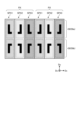
- FIG. 8 is an explanatory diagram for explaining the arrangement relationship between the first pixel circuits and the second pixel circuits of the plurality of sub-pixels according to the embodiment.
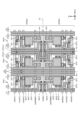
- FIG. 9 is a plan view schematically showing a configuration example of a plurality of sub-pixels according to the embodiment.
- FIG. 1 is a plan view showing a display device according to an embodiment.
- the display device 1 of the present embodiment is a micro LED display device including micro LEDs.
- the display device 1 includes an array substrate 2, a plurality of pixels PX, a scanning line driving circuit 12, a signal line driving circuit 13, a light emission control circuit 14, and a driving IC (Integrated Circuit) 210. and including.
- the array substrate 2 is a drive circuit substrate for driving each pixel PX, and is also called a backplane or active matrix substrate.
- the array substrate 2 is formed using a substrate 21 as a base, and has a plurality of thin film transistors, a plurality of capacitors, various wirings, etc. on the substrate 21 .
- a wiring board for example, a flexible printed circuit board (FPC)
- FPC flexible printed circuit board
- the first direction Dx is one direction within a plane parallel to the substrate 21 .
- the second direction Dy is one direction in a plane parallel to the substrate 21 and perpendicular to the first direction Dx. Note that the second direction Dy may not be perpendicular to the first direction Dx, but may intersect with it.
- a third direction Dz is a direction orthogonal to the first direction Dx and the second direction Dy, and is a normal direction of the substrate 21 . Also, "planar view” refers to the positional relationship when viewed from the third direction Dz.
- the scanning line driving circuit 12 drives a plurality of scanning lines (eg, reset control signal line L5, write control scanning line L7, initialization control signal line L8 (see FIG. 4)) based on various control signals from the driving IC 210. This is the circuit to drive.
- the scanning line driving circuit 12 sequentially or simultaneously selects a plurality of gate lines and supplies gate driving signals to the selected scanning lines. Thereby, the scanning line driving circuit 12 selects a plurality of pixels PX connected to the gate lines.
- the signal line drive circuit 13 applies potentials (video signal VSG, reset power supply potential Vrst, initialization potential Vini) to drive a plurality of pixels PX.
- the light emission control circuit 14 is a driving circuit that supplies signals to the scanning lines (the light emission control scanning line L6 and the connection control scanning line L9 (see FIG. 4)) of the display area AA to drive the plurality of pixels PX.
- the driving IC 210 is a circuit that supplies control signals to the scanning line driving circuit 12, the signal line driving circuit 13, and the light emission control circuit 14 to control the display of the plurality of pixels PX. At least part of the scanning line driving circuit 12, the signal line driving circuit 13, and the light emission control circuit 14 may be formed integrally with the driving IC 210. FIG. Also, the driving IC 210 is provided on the array substrate 2 . However, the present invention is not limited to this, and the drive IC 210 may be provided on a wiring board connected to the array substrate 2 .
- the array substrate 2 has a display area AA and a peripheral area GA.
- a plurality of pixels PX are provided in the display area AA.
- a plurality of pixels PX are arranged in a matrix in the display area AA.
- the peripheral area GA is an area outside the display area AA and is an area where a plurality of pixels PX are not provided.
- a scanning line driving circuit 12, a signal line driving circuit 13, a light emission control circuit 14, and a driving IC 210 are provided in the peripheral area GA.
- the scanning line driving circuit 12 and the light emission control circuit 14 are provided in an area extending along the second direction Dy in the peripheral area GA.
- the signal line driving circuit 13 and the driving IC 210 are provided in an area extending along the first direction Dx in the peripheral area GA. Note that the scanning line driving circuit 12 and the light emission control circuit 14 may be provided in an area along the same side of the peripheral area GA.
- the display area AA is divided into four parts, and the display on the display device 1 is divided into a first partial display area AAs1, a second partial display area AAs2, a third partial display area AAs3, and a fourth partial display area AAs4.
- An example of operation will be described (see FIG. 5).
- the display area AA has a rectangular shape
- the peripheral area GA has a rectangular frame shape surrounding the display area AA in order to make the description easier to understand.
- the display area AA is not limited to this, and may have a polygonal shape or an irregular shape having a notch or a curved portion in a part of the outer circumference.
- the peripheral area GA can also have various shapes corresponding to the shape of the display area AA.
- FIG. 2 is a plan view showing an example of pixels of the display device according to the embodiment.
- the pixel PX has a first sub-pixel SPX1, a second sub-pixel SPX2 and a third sub-pixel SPX3.
- the first sub-pixel SPX1, the second sub-pixel SPX2, and the third sub-pixel SPX3 each include a light emitting element 100.
- the light emitting element 100 is an inorganic light emitting diode (LED: Light Emitting Diode) chip having a size of about 3 ⁇ m or more and 300 ⁇ m or less in plan view, and is called a micro LED. Note that the micro of the micro LED does not limit the size of the light emitting element 100 .
- LED Light Emitting Diode
- the first sub-pixel SPX1, the second sub-pixel SPX2, and the third sub-pixel SPX3 are simply referred to as sub-pixels SPX when there is no need to distinguish them.
- the light emitting element 100 is arranged in the center of each sub-pixel SPX, FIG. 2 is only a schematic illustration, and the position of the light emitting element 100 in each sub-pixel SPX can be changed as appropriate. can.
- the first sub-pixel SPX1 displays red (R), for example.
- the second sub-pixel SPX2 displays green (G), for example.
- the third sub-pixel SPX3 displays blue (B), for example.
- the first sub-pixel SPX1, the second sub-pixel SPX2, and the third sub-pixel SPX3 are arranged side by side in the first direction Dx.
- the arrangement is not limited to this, and the pixels PX may be arranged in another arrangement.
- the first subpixel SPX1 and the second subpixel SPX2 are arranged adjacent to each other in the second direction Dy
- one third subpixel SPX3 is arranged adjacent to the first subpixel SPX1 and the second subpixel SPX2 in the second direction Dy.
- the pixels PX may be arranged adjacent to the sub-pixel SPX2 in the first direction Dx.
- the pixels PX may be configured in a so-called pentile array.
- the pixel PX is not limited to three sub-pixels SPX, and may be composed of four or more sub-pixels SPX.
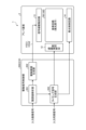
- FIG. 3 is a block diagram illustrating a configuration example of the display device according to the embodiment;
- the display device 1 has a pixel circuit 50 and a drive signal control section 200 that controls driving of the pixel circuit 50 .
- the pixel circuit 50 is a circuit that supplies a drive signal (current) to the light emitting element 100 to drive the light emitting element 100 .
- FIG. 3 schematically shows one pixel circuit 50 (light emitting element 100), a plurality of pixel circuits 50 and a plurality of light emitting elements 100 are provided for each sub-pixel SPX (see FIG. 2). They are arranged in a matrix in the display area AA.
- the drive signal control unit 200 includes a gradation value analysis unit 201, a drive gradation generation unit 202, and a timing signal generation unit 203.
- a gradation value analysis unit 201 is a circuit that calculates a gradation value (hereinafter sometimes referred to as a target luminance level) for each pixel PX (sub-pixel SPX) based on an image signal input from an external control circuit. be.
- the drive gradation generation unit 202 is a circuit that generates the first video signal VSG1 and the second video signal VSG2 based on the target luminance level received from the gradation value analysis unit 201.
- the signal line driving circuit 13 of the array substrate 2 outputs the first video signal VSG1 and the second video signal VSG2 supplied from the driving gradation generation unit 202 to the pixel circuit 50, and controls the plurality of pixels PX at the target luminance level. drive.
- the video signal VSG when there is no need to distinguish between the first video signal VSG1 and the second video signal VSG2, they may simply be referred to as the video signal VSG.
- the timing signal generation section 203 generates a timing signal based on the synchronization signal input from the external control circuit and the target luminance level received from the gradation value analysis section 201 .
- the scanning line driving circuit 12 and the light emission control circuit 14 generate control signals (write control signal SG, light emission control signal BG, etc.) to the pixel circuit 50 based on the timing signal (control signal) supplied from the timing signal generation unit 203 . to output
- the first video signal VSG1 and the second video signal VSG2 have predetermined signal potentials for lighting the light-emitting element 100 .
- the timing signal (control signal) supplied from the timing signal generator 203 includes information about the lighting period of the light emitting element 100 by the light emission control circuit 14 .
- the display device 1 has a method of expressing gradation by controlling the current value supplied to the light emitting element 100 of each sub-pixel SPX (hereinafter referred to as a current driving method or an analog driving method), and Multi-gradation display can be performed by combining a method of expressing gradation by controlling the lighting time while keeping the current value constant (hereinafter referred to as PWM driving method or pulse width modulation method).
- the drive signal control section 200 may be formed integrally with the drive IC 210, or may be provided in an external control circuit.
- FIG. 4 is a circuit diagram showing a configuration example of a pixel circuit.
- the pixel circuit 50 includes a first pixel circuit 50a and a second pixel circuit 50b.
- the first pixel circuit 50 a and the second pixel circuit 50 b are connected to one light emitting element 100 . That is, the first pixel circuit 50a and the second pixel circuit 50b are provided for each sub-pixel SPX.
- the first pixel circuit 50a is a circuit that drives the light emitting element 100 by a current driving method. Note that the first pixel circuit 50a can be shared as a circuit that drives the light emitting element 100 by the PWM driving method during a part of the frame period during which one screen is displayed.
- the second pixel circuit 50b is a circuit that drives the light emitting element 100 by the PWM driving method.
- the first pixel circuit 50a includes a first emission control transistor BCT1, a first write transistor SST1, a first drive transistor DRT1, a first initialization transistor IST1, a first reset transistor RST1 and a first connection switching transistor CNT1.
- Each of the plurality of thin film transistors included in the first pixel circuit 50a is composed of an n-type TFT (Thin Film Transistor).
- the first pixel circuit 50a also includes a first storage capacitor Cs1 and a first additional capacitor Cad1.
- the gate of the first emission control transistor BCT1 is connected to the first emission control scanning line L6a.
- a first emission control signal BG1 is supplied to the first emission control scanning line L6a.
- One of the source and the drain of the first emission control transistor BCT1 is connected to the first anode power line L1a, and the power supply voltage PVDD is supplied from the first anode power line L1a.
- the other of the source and drain of the first emission control transistor BCT1 is connected to the first drive transistor DRT1.
- the power supply voltage PVDD is supplied to the first drive transistor DRT1.
- the gate of the first write transistor SST1 is connected to the first write control scanning line L7a.
- a first write control signal SG1 is supplied to the first write control scanning line L7a.
- One of the source and drain of the first write transistor SST1 is connected to the first video signal line L2a.
- the other of the source and drain of the first write transistor SST1 is connected to the gate of the first drive transistor DRT1.
- the first video signal VSG1 is supplied from the signal line drive circuit 13 to the gate of the first drive transistor DRT1.
- the ON state of the drive transistor DRT changes according to the magnitude of the first video signal VSG1.
- the first video signal VSG1 corresponds to the signal potential at which the light emitting element 100 has the maximum luminance
- the driving transistor DRT is almost completely turned on in accordance with the potential of the first video signal VSG1, and the power supply voltage PVDD.
- the current (predetermined fixed potential) from the DRT passes through the driving transistor DRT and is supplied to the light emitting element 100 almost as it is.
- the driving transistor DRT is turned off, and the current from the power supply voltage PVDD is not supplied to the light-emitting element 100. .
- the ON state of the driving transistor DRT changes in magnitude according to the signal potential of the first video signal VSG1, and as a result, the current from the power supply voltage PVDD is only the amount corresponding to the ON state of the driving transistor DRT. It is supplied to the light emitting element 100 .
- the gate of the first initialization transistor IST1 is connected to the first initialization control signal line L8a.
- a first initialization control signal IG1 is supplied to the first initialization control signal line L8a.
- One of the source and drain of the first initialization transistor IST1 is connected to the first initialization power supply line L4a.
- the other of the source and drain of the first initialization transistor IST1 is connected to the gate of the first drive transistor DRT1 and the other of the source and drain of the first write transistor SST1.
- An initialization potential Vini is supplied to the first initialization power supply line L4a. That is, when the first initialization transistor IST1 is turned on (conducting state), the gate of the driving transistor DRT is supplied with the initialization potential Vini via the first initialization transistor IST1.
- the gate of the first reset transistor RST1 is connected to the first reset control signal line L5a.
- a first reset control signal RG1 is supplied to the first reset control signal line L5a.
- One of the source and the drain of the first reset transistor RST1 is connected to the first reset power supply line L3a.
- the other of the source and drain of the first reset transistor RST1 is connected to the source of the first drive transistor DRT1 (node N1 on the output side).
- a reset power supply potential Vrst is supplied to the first reset power supply line L3a. That is, when the first reset transistor RST1 is turned on (conducting state), the source of the drive transistor DRT (node N1 on the output side) is supplied with the reset power supply potential Vrst via the first reset transistor RST1.
- the gate of the first connection switching transistor CNT1 is connected to the first connection control scanning line L9a.
- a first connection control signal PWM1 is supplied to the first connection control scanning line L9a.
- One of the source and drain of the first connection switching transistor CNT1 is connected to the source of the first drive transistor DRT1 (node N1 on the output side) via the node N1 on the output side.
- the other of the source and drain of the first connection switching transistor CNT1 is connected to the anode 23 of the light emitting element 100.
- FIG. In other words, the first connection switching transistor CNT1 is connected between the first drive transistor DRT1 and the light emitting element 100.
- a power supply voltage PVSS is supplied to the cathode of the light emitting element 100 through a cathode power supply line L10.
- the light emitting element 100 is supplied with a forward current (driving current) by a potential difference (PVDD-PVSS) between the power supply voltage PVDD supplied to the anode and the power supply voltage PVSS supplied to the cathode to emit light.
- PVDD-PVSS potential difference
- the first write control scanning line L7a, the first initialization control signal line L8a, and the first reset control signal line L5a are connected to the scanning line driving circuit 12 shown in FIG.
- the scanning line drive circuit 12 supplies various control signals to the first write control scanning line L7a, the first initialization control signal line L8a, and the first reset control signal line L5a.
- the first light emission control scanning line L6a and the first connection control scanning line L9a are connected to the light emission control circuit .
- the light emission control circuit 14 supplies control signals to the first light emission control scanning line L6a and the first connection control scanning line L9a.
- the first storage capacitor Cs1 of the first pixel circuit 50a is a capacitor formed between the gate and source (node N1 on the output side) of the first drive transistor DRT1.
- the first additional capacitance Cad1 is a capacitance formed between the output side node N1 and the first cathode power supply line L10a.
- the second pixel circuit 50b includes a second emission control transistor BCT2, a second write transistor SST2, a second drive transistor DRT2, a second initialization transistor IST2, a second reset transistor RST2 and a second connection switching transistor CNT2.
- the second pixel circuit 50b includes a second anode power line L1b, a second video signal line L2b, a second reset power line L3b, a second initialization power line L4b, a second reset control signal line L5b, and a second emission control scanning line.
- the second pixel circuit 50b has a configuration similar to that of the first pixel circuit 50a, and repeated description will be omitted.
- the second emission control transistor BCT2 when the second emission control transistor BCT2 is turned on (conducting state), the power supply voltage PVDD is supplied to the second drive transistor DRT2.
- the gate of the second connection switching transistor CNT2 is connected to the second connection control scanning line L9b.
- a second connection control signal PWM2 is supplied to the second connection control scanning line L9b.
- One of the source and drain of the second connection switching transistor CNT2 is connected to the second drive transistor DRT2.
- the other of the source and drain of the second connection switching transistor CNT2 is connected to the anode 23 of the light emitting element 100.
- FIG. In other words, the second connection switching transistor CNT2 is connected between the second drive transistor DRT2 and the light emitting element 100.
- the second pixel circuit 50b includes a second storage capacitor Cs2 and a second additional capacitor Cad2.
- the second storage capacitor Cs2 is a capacitor formed between the gate and source (node N2 on the output side) of the second drive transistor DRT2.
- the second additional capacitance Cad2 is a capacitance formed between the node N2 on the output side and the second cathode power supply line L10b.
- each wiring (first anode power supply line L1a to first cathode power supply line L10a) of the first pixel circuit 50a and each wiring (second power supply line L10a) of the second pixel circuit 50b are shown.
- the anode power supply line L1b to the second cathode power supply line L10b) are shown separately for each circuit.
- the first pixel circuit 50a and the second pixel circuit 50b may share part of the wiring.
- the light emission control transistor BCT and the writing transistor are simply used. They may be represented as SST, drive transistor DRT, initialization transistor IST, reset transistor RST, and connection switching transistor CNT.
- anode power supply line L1, the video signal line L2, and the reset power supply line L3 are simply referred to as the anode power line L1, the video signal line L2, and the reset power line L3.
- an initialization power supply line L4 a reset control signal line L5, an emission control scanning line L6, a write control scanning line L7, an initialization control signal line L8, a connection control scanning line L9, and a cathode power supply line L10.
- the light emission control signal BG and the write control signal are simply Signal SG, initialization control signal IG, reset control signal RG, and connection control signal PWM may be used.
- FIG. 5 is a timing chart for explaining an operation example of the display device according to the embodiment. Note that FIG. 5 shows the operation of driving the sub-pixels SPX in the first partial display area AAs1 and the second partial display area AAs2. driven by Also, in the following description, a period during which the sub-pixels SPX in the first row to the sub-pixels SPX in the last row are driven is referred to as a frame period.
- the period t1 is the video signal writing operation period for the first partial display area AAs1.
- each control signal supplied from the scanning line driving circuit 12 and the emission control circuit 14 controls the potential of the first emission control scanning line L6a and the second emission control scanning line L6b (first emission control signal BG1 and second light emission control signal BG2) become L level, and the potentials of write control scanning lines L7-1, L7-2, .
- the control signal SG2) becomes H level.
- the first emission control transistor BCT1 of the first pixel circuit 50a and the second emission control transistor BCT2 of the second pixel circuit 50b are turned off.
- the first write transistor SST1 of the first pixel circuit 50a and the second write transistor SST2 of the second pixel circuit 50b are turned on.
- the write control scanning lines L7 belonging to the first partial display area AAs1 are sequentially scanned.
- the write control scanning line L7-1 is the write control scanning line L7 connected to the sub-pixels SPX on the first row
- the write control scanning line L7-2 is connected to the sub-pixels SPX on the second row. This is the write control scanning line L7.
- the first partial display area AAs1 is an area including, for example, the write control scanning line L7-1 to the write control scanning line L7-270.
- FIG. 6 is a timing chart for explaining an operation example during the write period shown in FIG.
- FIG. 6 shows the video signal writing operation period SW shown in period t4 in FIG. 5 in an enlarged manner. It can also be applied during the busy operation period. Note that in the period before the period t1, the sub-pixel SPX continues the light emitting state of the previous frame.
- period t11 is the source initialization period of the drive transistor DRT.
- each control signal supplied from the scanning line drive circuit 12 and the emission control circuit 14 causes the potential of the emission control scanning line L6 (the first emission control signal BG1 and the second emission control signal BG2) to becomes L level, and the potential of the reset control signal line L5 (first reset control signal RG1 and second reset control signal RG2) becomes H level.
- the light emission control transistor BCT is turned off (non-conducting state), and the reset transistor RST is turned on (conducting state).
- the first connection control signal PWM1 and the second connection control signal PWM2 are at L level from period t11 to period t17, and the connection switching transistor CNT is turned off. That is, the light emitting element 100 is disconnected from the first pixel circuit 50a and the second pixel circuit 50b during the video signal writing operation period, which is the non-light emitting period of the light emitting element 100.
- FIG. As a result, it is possible to prevent the potentials generated at the node N1 of the first pixel circuit 50a and the node N2 of the second pixel circuit 50b from being applied to the light emitting element 100 during the video signal writing operation period. Unintended application of a reverse bias potential to the light emitting element 100 can be suppressed, and damage to the light emitting element 100 can be suppressed.
- the current from the anode power supply line L1 is cut off by the light emission control transistor BCT, and the connection switching transistor CNT is turned off as described above.
- the light emission of the light emitting element 100 stops, the charge remaining in the sub-pixel SPX flows to the outside through the reset transistor RST.
- the source of the drive transistor DRT is fixed to the reset power supply potential Vrst.
- period t12 is the gate initialization period of the drive transistor DRT.
- each control signal supplied from the scanning line driving circuit 12 and the light emission control circuit 14 changes the potential of the initialization control signal line L8 (the first initialization control signal IG1 and the second initialization control signal The signal IG2) becomes H level.
- the initialization transistor IST is turned on.
- the gate of the drive transistor DRT is fixed to the initialization potential Vini through the initialization transistor IST.
- the initialization potential Vini has a potential higher than the threshold of the driving transistor DRT with respect to the reset power supply potential Vrst. Therefore, the drive transistor DRT is turned on.
- the light emission control transistor BCT is kept off, so no current flows through the drive transistor DRT.
- period t13 is the offset cancellation operation period. Specifically, in the period t13, each control signal supplied from the scanning line driving circuit 12 and the emission control circuit 14 causes the potential of the emission control scanning line L6 (the first emission control signal BG1 and the second emission control signal BG2) to becomes H level, and the potential of the reset control signal line L5 (first reset control signal RG1 and second reset control signal RG2) becomes L level. As a result, the light emission control transistor BCT is turned on, and the reset transistor RST is turned off.
- the drive transistor DRT is in the ON state due to the operation during period t12. Therefore, a current is supplied from the anode power supply line L1 (power supply voltage PVDD) to the drive transistor DRT via the light emission control transistor BCT.
- L1 power supply voltage PVDD
- connection switching transistor CNT is off, and no current flows to the light emitting element 100 side. Therefore, the source of the drive transistor DRT is charged by the power supply voltage PVDD, and the potential of the source increases.
- the gate potential of the drive transistor DRT is the initialization potential Vini. Therefore, when the source potential of the drive transistor DRT reaches (Vini-Vth), the drive transistor DRT is turned off and the potential stops rising.
- Vth is the threshold voltage Vth of the drive transistor DRT.
- the threshold voltage Vth varies for each sub-pixel SPX (and for each pixel circuit 50). Therefore, the potential of the source of the driving transistor DRT when the potential stops increasing differs for each sub-pixel SPX (and for each pixel circuit 50). That is, a voltage corresponding to the threshold voltage Vth of the driving transistor DRT is obtained in each subpixel SPX by the operation in period t13.
- each control signal supplied from the scanning line drive circuit 12 and the light emission control circuit 14 changes the potential of the write control scanning line L7 (the first write control signal SG1 and the second write control signal SG2 ) becomes H level.
- the light emission control transistor BCT is turned off, the initialization transistor IST is turned off, and the write transistor SST is turned on.
- the video signal VSG is input to the gate of the drive transistor DRT in the sub-pixel SPX belonging to the first partial display area AAs1.
- the gate potential of the driving transistor DRT changes from the initialization potential Vini to the potential of the video signal VSG.
- the potential of the source of the driving transistor DRT is maintained at (Vini-Vth).
- the voltage between the gate and source of the driving transistor DRT becomes (VSG-(Vini-Vth)), reflecting the variation in the threshold voltage Vth between the sub-pixels SPX.
- the first video signal VSG1-1 is applied to the first pixel. It is input to the gate of the first drive transistor DRT1 of the circuit 50a. Due to the video signal write operation in period t1, the gate potential of the first drive transistor DRT1 changes to the potential of the first video signal VSG1-1.
- the second video signal VSG2-1 is input to the gate of the second driving transistor DRT2 of the second pixel circuit 50b. The gate potential of the second drive transistor DRT2 changes to the potential of the second video signal VSG2-1.
- periods t1a and t1b after period t1 are light emitting operation periods.
- display is performed by a so-called PWM driving method based on the first video signal VSG1-1 and the second video signal VSG2-1.
- the PWM driving method expresses the gradation of the light emitting element 100 according to the length of the pulse width of the light emission control signal BG output from the light emission control circuit 14 to each light emission control scanning line L6.
- the brightness is preferably the maximum luminance of the light emitting element 100 .
- the video signals input in the period t1 are all video signals VSG (signal potential) corresponding to the so-called maximum luminance of the light emitting element 100 .
- VSG signal potential
- the gradation of the light emitting element 100 is controlled at the maximum luminance or 0 luminance during the period of the PWM driving method.
- the video signal VSG supplied during the display period by the PWM driving method may be expressed as a digital signal.
- the first emission control signal BG1 supplied to the first emission control scanning line L6a becomes H level by each control signal supplied from the scanning line driving circuit 12 and the emission control circuit 14,
- the second emission control signal BG2 supplied to the second emission control scanning line L6b becomes L level.
- L7-270 of the first partial display area AAs1 are at L level.
- the first emission control transistor BCT1 of the first pixel circuit 50a is turned on, and the first write transistor SST1 is turned off. Furthermore, during the light emitting period, the first connection switching transistor CNT1 is turned on.
- a power supply voltage PVDD is supplied to the first drive transistor DRT1 through the first light emission control transistor BCT1.
- the first drive transistor DRT1 supplies the light emitting element 100 with a current corresponding to the voltage between the gate and the source set in the period t1. That is, the first driving transistor DRT1 is almost completely turned on by the video signal, and the light emitting element 100 emits light with the maximum luminance due to the potential difference of PVDD-PVSS.
- period t1a the period (pulse width) during which the first light emission control transistor BCT1 is turned on is set to a period in which the target luminance level is 12.5% of the maximum lighting luminance. Note that during the period t1a, the second light emission control transistor BCT2 of the second pixel circuit 50b is off, so no current flows from the second drive transistor DRT2 to the light emitting element 100. FIG. However, the voltage between the gate and source of the second drive transistor DRT2 is held by the second holding capacitor Cs2.
- the second connection switching transistor CNT2 of the second pixel circuit 50b is off, so that the voltage fluctuation between the gate and the source of the second driving transistor DRT2 due to the current from the first driving transistor DRT1 is suppressed. be done.
- the control signals supplied from the scanning line drive circuit 12 and the emission control circuit 14 cause the first emission control signal BG1 supplied to the first emission control scanning line L6a to be at L level.
- the second emission control signal BG2 supplied to the emission control scanning line L6b becomes H level.
- the second emission control transistor BCT2 of the second pixel circuit 50b is turned on, and the second write transistor SST2 is turned off. Furthermore, the second connection switching transistor CNT2 is turned on.
- a power supply voltage PVDD is supplied to the second drive transistor DRT2 through the second light emission control transistor BCT2.
- the second drive transistor DRT2 supplies the light emitting element 100 with a current corresponding to the voltage between the gate and the source set in the period t1. That is, the second driving transistor DRT2 is almost completely turned on by the digital signal, and the light emitting element 100 emits light with maximum luminance based on the potential difference of PVDD-PVSS.
- the period (pulse width) during which the second emission control transistor BCT2 is turned on is set to a period in which the target luminance level is 50% of the maximum lighting luminance. That is, the period t1b is longer than the period t1a, and corresponds to four times the period t1a in this embodiment.
- the first light emission control transistor BCT1 of the first pixel circuit 50a is off, no current flows from the first drive transistor DRT1 to the light emitting element 100.
- both periods t1a and t1b which are light emission periods
- the light emitting element 100 is illuminated at maximum luminance.
- the period t1a is shorter than the period 1b. Therefore, the luminance of the light-emitting element 100 can be changed by switching on/off of the light-emitting element 100 in the periods t1a and t1b. More specifically, if the light-emitting element 100 is lit at maximum luminance in both periods t1a and t1b, the user of the display device 1 will not be able to see the period t1a and the period t1b due to the integration effect of the human eye.
- the light-emitting element 100 is visually recognized as being lit with the brightest luminance during a period of 100 seconds (the luminance at this time is defined as luminance A).
- the light-emitting element 100 is lit only in the period t1a in the period t1a and the period t1b, even if the light-emitting element 100 is lit at the maximum luminance in the period t1a, the integration effect in the time axis direction When viewed over the entire period of period t1a and period t1b, the light is darker than the luminance B, and the user perceives that the light emitting element 100 is lit with the luminance C which is darker than the luminance B.
- the luminance is changed according to the length of the lighting period of the light emitting element 100 .
- the video signal write operations for the second partial display area AAs2 to the fourth partial display area AAs4 are sequentially performed.
- the light emitting operation of the second partial display area AAs2 is performed in the same manner as the first partial display area AAs1.
- the video signal writing operation for the first partial display area AAs1 is performed in the same manner as during period t1. Due to the video signal write operation in period t4, the gate potential of the first drive transistor DRT1 changes to the potential of the first video signal VSG1-2. The gate potential of the second drive transistor DRT2 changes to the potential of the second video signal VSG2-2.
- the control signals supplied from the scanning line driving circuit 12 and the emission control circuit 14 cause the first emission control signal BG1 supplied to the first emission control scanning line L6a to be at L level.
- the second emission control signal BG2 supplied to the emission control scanning line L6b becomes H level.
- a period t4a following the period t4 is one period of display by the PWM driving method.
- period t4b is a display period using analog gradation.
- Display using analog gradation means that while the lighting period is fixed to a predetermined period, the pixel signal (video signal VSG) has an analog potential, and the ON state of the gate of the driving transistor DRT is adjusted according to the analog potential, and the power supply is turned on.
- a current from the voltage PVDD to the light emitting element 100 has a magnitude corresponding to the ON state of the gate. As a result, the luminance of the light emitting element 100 becomes brightness corresponding to the analog potential of the pixel signal (video signal VSG).
- the brightness of the light-emitting element 100 based on the analog potential pixel signal has any brightness from brightness 0 to a predetermined brightness.
- this period is a PWM drive period
- the light emitting element 100 emits light only at the maximum luminance or 0 luminance over the period. It emits light with any luminance between 0 and maximum luminance depending on the gradation representation by .
- the display by analog gradation may be referred to as an analog driving method.
- the pixel signal supplied to the pixel circuit 50 during the display period by the analog driving method can be set corresponding to the so-called 0 to 255 gradations. 12.5% of the entire lighting period, the luminance expression by the pixel signal is about 0 to 32 gradations.
- period t4a the period (pulse width) during which the second light emission control transistor BCT2 is turned on is set to a period in which the target luminance level is 25% of the maximum lighting luminance.
- period t4a since the first light emission control transistor BCT1 of the first pixel circuit 50a is off, no current flows from the first drive transistor DRT1 to the light emitting element 100.
- the first emission control signal BG1 supplied to the first emission control scanning line L6a becomes H level by each control signal supplied from the scanning line driving circuit 12 and the emission control circuit 14, and the second emission control signal BG1 becomes H level.
- the second emission control signal BG2 supplied to the emission control scanning line L6b becomes L level.
- a current (first drive current) corresponding to the first video signal VSG1-2 which is an analog signal, is supplied to the light emitting element 100 from the first drive transistor DRT1.
- the period (pulse width) during which the first light emission control transistor BCT1 is turned on is fixed to the period during which the target luminance level is 12.5% of the maximum lighting luminance.
- the potential of the first video signal VSG1-2 in the period t4b is set by the drive signal control section 200 for each sub-pixel SPX.
- the second light emission control transistor BCT2 of the second pixel circuit 50b is off, so no current flows from the second drive transistor DRT2 to the light emitting element 100.
- the drive signal control section 200 can control the brightness (grayscale) of the light emitting element 100 by the sum of the light emitting operation periods of periods t1a and t1b and periods t4a and t4b. More specifically, the brightness of the optical element is reduced to 87.5 by the display period by the PWM driving method based on the digital potential video signals (first video signal VSG1-1, second video signals VSG2-1, VSG2-2). %, and the remaining 12.5% of the luminance is constituted by the analog potential video signals (first video signals VSG1-2). Further, the brightness of the 12.5% luminance can be set more finely according to the analog potential. Therefore, by combining the PWM driving system period and the analog driving system period, extremely fine gradation expression can be realized.
- the example shown in FIG. 5 shows a case where current flows through the light emitting element 100 during the entire period of periods t1a, t1b and periods t4a, t4b, and 100% luminance is displayed.
- the drive signal control unit 200 controls the lighting on/off of the periods t1a and t1b and the periods t4a and t4b, so that the fixed current is supplied to the light emitting element for a period corresponding to the video signal VSG. 100 supplies.
- the current (first video signal VSG1-2) in the period t4b it is possible to appropriately control the brightness (gradation).
- the first connection switching transistor CNT1 is on/off controlled in synchronization with the first light emission control transistor BCT1.
- the second connection switching transistor CNT2 is on/off controlled in synchronization with the second light emission control transistor BCT2.
- FIG. 7 is an explanatory diagram for explaining an example of a combination of the current driving method and the PWM driving method for each display luminance level.
- the drive signal control section 200 turns on the first light emission control transistor BCT1 in the period t4b, causing the current (second 1 video signal VSG1-2) is supplied to the light emitting element 100 to adjust the lighting luminance level. That is, the drive signal control section 200 turns off the first emission control transistor BCT1 and the second emission control transistor BCT2 during periods t1a, t1b, and t4a. That is, in the above description, the light-emitting element 100 is off (not emitting light) during periods t1a, t1b, and t4a.
- the drive signal control section 200 turns on the first light emission control transistor BCT1 in period t1a to correspond to the target luminance level of 12.5%.
- a current (first video signal VSG1-1) is supplied to the light emitting element 100 for a period of time.
- the drive signal control unit 200 turns on the first light emission control transistor BCT1 in the period t4b to supply the current (the first video signal VSG1-2) to the light emitting element 100, and the current is 12.5% to 25% or less.
- the drive signal control section 200 turns on the second light emission control transistor BCT2 in the period t4a to provide a length corresponding to the target luminance level of 25%.
- a current (second video signal VSG2-2) is supplied to the light emitting element 100 during this period.
- the drive signal control unit 200 turns on the first light emission control transistor BCT1 in the period t4b, supplies the current (first video signal VSG1-2) to the light emitting element 100, and reduces the current from 25% to 37.5% or less. Adjust the lighting brightness level in the range of .
- the drive signal control section 200 turns off the first emission control transistor BCT1 and the second emission control transistor BCT2 during the periods t1a and t1b. That is, in the above description, the light-emitting element 100 is off (not emitting light) during the periods t1a and t1b.
- the drive signal control section 200 turns on the first emission control transistor BCT1 and the second emission control transistor BCT2 in periods t1a and t4a, respectively. , the current (first video signal VSG1-1, second video signal VSG2-2 ) is supplied to the light emitting element 100 . Further, the drive signal control unit 200 turns on the first light emission control transistor BCT1 in the period t4b to supply the current (first video signal VSG1-2) to the light emitting element 100, and the current is 37.5% to 50% or less. Adjust the lighting brightness level in the range of .
- the drive signal control section 200 turns off the first emission control transistor BCT1 and the second emission control transistor BCT2 in the period t1b. That is, in the above description, the light emitting element 100 is off (not emitting light) during the period t1b.
- the driving signal control unit 200 combines the current (first video signal VSG1-1, second video signals VSG2-1, VSG2-2) and current (first video signal VSG1-2) to Display of brightness level can be realized.
- FIG. 8 is an explanatory diagram for explaining the arrangement relationship between the first pixel circuits and the second pixel circuits of the plurality of sub-pixels according to the embodiment.
- the first sub-pixel SPX1, the second sub-pixel SPX2, and the third sub-pixel SPX3 are hatched.
- the L-shaped pattern shown in each subpixel SPX is for schematically explaining the arrangement relationship (symmetry of arrangement) of each transistor and each wiring included in a plurality of subpixels SPX. Also, it does not represent the arrangement pattern or shape of each wiring.
- the plurality of pixels PX are arranged in the first direction Dx.
- the first sub-pixel SPX1, the second sub-pixel SPX2, the third sub-pixel SPX3, the first sub-pixel SPX1, the second sub-pixel SPX2, and the third sub-pixel SPX3 are repeatedly arranged in this order.
- the first pixel circuit 50a and the second pixel circuit 50b are arranged adjacent to each other in the second direction Dy.
- the arrangement pattern of each transistor and each wiring of the first pixel circuit 50a is the arrangement pattern of each transistor and each wiring of the second pixel circuit 50b. They are arranged line-symmetrically with an axis of symmetry parallel to the first direction Dx.
- the arrangement pattern of each transistor and each wiring of the first pixel circuit 50a is vertically inverted with respect to the arrangement pattern of each transistor and each wiring of the second pixel circuit 50b. layout pattern.
- one subpixel SPX (first subpixel SPX1) ) and the first pixel circuit 50a and the second pixel circuit 50b of the other sub-pixel SPX (second sub-pixel SPX2) are symmetrical parallel to the second direction Dy. They are arranged symmetrically about the axis.
- the arrangement pattern of each transistor and each wiring of the first pixel circuit 50a and the second pixel circuit 50b in two adjacent sub-pixels SPX is a horizontally inverted arrangement pattern.
- the first sub-pixel SPX1 of one pixel PX (pixel PX on the left side in FIG. 8) and the pixel PX of the other pixel PX (pixel PX on the right side in FIG. 8) ) has an arrangement pattern that is left-right reversed from that of the first sub-pixel SPX1. That is, in the first direction Dx, the first sub-pixel SPX1, the second sub-pixel SPX2, the third sub-pixel SPX3, the first sub-pixel SPX1, the second sub-pixel SPX2, and the third sub-pixel SPX3 are repeatedly arranged in this order.
- the first pixel circuit 50a and the second pixel circuit 50b of one first subpixel SPX1 and the other first subpixel SPX1 are connected.
- the first pixel circuit 50a and the second pixel circuit 50b of the pixel SPX1 are arranged line-symmetrically with respect to the axis of symmetry parallel to the second direction Dy.
- FIG. 9 is a plan view schematically showing a configuration example of a plurality of sub-pixels according to the embodiment.
- FIG. 9 shows a configuration example of the first sub-pixel SPX1, the second sub-pixel SPX2, and the third sub-pixel SPX3 arranged in the first direction Dx.
- the electrical connection relationship between each transistor and each wiring of the first pixel circuit 50a and the second pixel circuit 50b shown in FIG. 9 is the same as that described above with reference to FIG. 4, and duplicate description will be omitted.
- each transistor of the first pixel circuit 50a and each transistor of the second pixel circuit 50b are parallel to the first direction Dx. are arranged line-symmetrically with respect to the symmetry axis Q1. More specifically, in the first pixel circuit 50a, the first reset transistor RST1, the first connection switching transistor CNT1, and the first drive transistor DRT1 are arranged from the axis of symmetry Q1 toward one side of the second direction Dy (upper side in FIG. 9). , the first emission control transistor BCT1, the first write transistor SST1, and the first initialization transistor IST1.
- the second reset transistor RST2, the second connection switching transistor CNT2, the second drive transistor DRT2, and the second light emission are arranged from the axis of symmetry Q1 toward the other side of the second direction Dy (lower side in FIG. 9).
- the control transistor BCT2, the second write transistor SST2, and the second initialization transistor IST2 are arranged in this order.
- the light emitting element 100 (not shown in FIG. 9) is connected to the first connection switching transistor CNT1 via the contact CH1, and is connected to the second connection switching transistor CNT2 via the contact CH2.
- Each wiring of the first pixel circuit 50a and each wiring of the second pixel circuit 50b are arranged line-symmetrically with respect to the symmetry axis Q1 parallel to the first direction Dx. More specifically, in the first pixel circuit 50a, the reset control signal line L5, the first connection control scanning line L9a, the first light emission control line L5, the first connection control scanning line L9a, and the first light emission control line L5 are arranged from the axis of symmetry Q1 toward one side of the second direction Dy (upper side in FIG. 9).
- the scanning line L6a, the first write control scanning line L7a, and the first initialization control signal line L8a are arranged in this order.
- the reset control signal line L5 the second connection control scanning line L9b, the second emission control scanning line L6b, The second write control scanning line L7b and the second initialization control signal line L8b are arranged in this order.
- one reset control signal line L5 is shared by the first pixel circuit 50a and the second pixel circuit 50b. That is, the first reset transistor RST1 of the first pixel circuit 50a and the second reset transistor RST2 of the second pixel circuit 50b are arranged adjacent to each other in the second direction Dy across the reset control signal line L5. The gate of the first reset transistor RST1 of the first pixel circuit 50a and the gate of the second reset transistor RST2 of the second pixel circuit 50b are connected to a common reset control signal line L5.
- the first pixel circuit of one of the sub-pixels SPX (the first sub-pixel SPX1) 50a and the second pixel circuit 50b, and the first pixel circuit 50a and the second pixel circuit 50b of the other sub-pixel SPX (second sub-pixel SPX2) are aligned with respect to the axis of symmetry Q2 parallel to the second direction Dy.
- arranged symmetrically That is, each transistor of the first sub-pixel SPX1 and each transistor of the second sub-pixel SPX2 are arranged line-symmetrically with respect to the axis of symmetry Q2.
- the axis of symmetry Q2 is located between the first video signal line L2a connected to the first sub-pixel SPX1 and the first video signal line L2a connected to the second sub-pixel SPX2.
- CNT, drive transistor DRT, light emission control transistor BCT, initialization transistor IST, and write transistor SST have a laterally reversed arrangement relationship with respect to axis of symmetry Q2.
- the first sub-pixel SPX1 has a reset power line L3, a second video signal line L2b, an anode power line L1, and a first video signal line L2a.
- the reset power line L3, the second video signal line L2b, the anode power line L1, and the first video signal line L2a are arranged in this order in the first direction Dx.
- a connection switching transistor CNT, a drive transistor DRT, a light emission control transistor BCT, an initialization transistor IST, and a write transistor SST are arranged between the second video signal line L2b and the anode power supply line L1 adjacent in the first direction Dx.
- the reset transistor RST is arranged between the reset power supply line L3 and the second video signal line L2b.
- the reset power line L3 is shared by the first pixel circuit 50a and the second pixel circuit 50b of the first sub-pixel SPX1. That is, in one first sub-pixel SPX1, the first reset transistor RST1 of the first pixel circuit 50a and the second reset transistor RST2 of the second pixel circuit 50b are connected to the common reset power line L3. Also, the anode power line L1 is shared by the first pixel circuit 50a and the second pixel circuit 50b of the first sub-pixel SPX1. That is, in one first sub-pixel SPX1, the first emission control transistor BCT1 of the first pixel circuit 50a and the second emission control transistor BCT2 of the second pixel circuit 50b are connected to the common anode power line L1. Also, the first video signal line L2a is provided corresponding to the first pixel circuit 50a of the first sub-pixel SPX1. The second video signal line L2b is provided corresponding to the second pixel circuit 50b of the first sub-pixel SPX1.
- the second sub-pixel SPX2 Focusing on the second sub-pixel SPX2 adjacent to the first sub-pixel SPX1 in the first direction Dx, the second sub-pixel SPX2 includes the first video signal line L2a, the anode power line L1, the second video signal line L2b, and the initialization It has a power line L4.
- the first video signal line L2a, the anode power line L1, the second video signal line L2b, and the initialization power line L4 are arranged in this order in the first direction Dx.
- the initialization power line L4 is shared by the first pixel circuit 50a and the second pixel circuit 50b of the first sub-pixel SPX1.
- the anode power line L1 is shared by the first pixel circuit 50a and the second pixel circuit 50b of the second sub-pixel SPX2.
- the first video signal line L2a is provided corresponding to the first pixel circuit 50a of the second sub-pixel SPX2.
- the second video signal line L2b is provided corresponding to the second pixel circuit 50b of the second sub-pixel SPX2.
- the first video signal line L2a, the anode power line L1 and the second video signal line L2b are arranged line-symmetrically with respect to the axis of symmetry Q2.
- the reset power line L3 of the first sub-pixel SPX1 and the initialization power line L4 of the second sub-pixel SPX2 are arranged asymmetrically with respect to the axis of symmetry Q2.
- the reset power line L3 and the initialization power line L4 are shared by two sub-pixels SPX adjacent in the first direction Dx. This makes it possible to reduce the arrangement pitch of the plurality of sub-pixels SPX in the first direction Dx compared to the case where each sub-pixel SPX is provided with the reset power line L3 and the initialization power line L4.
- the first pixel circuit 50a and the second pixel circuit 50b of one subpixel SPX (second subpixel SPX2) and the other subpixel SPX (third subpixel The first pixel circuit 50a and the second pixel circuit 50b of SPX3) are arranged line-symmetrically with respect to the axis of symmetry Q3 parallel to the second direction Dy.
- each transistor and each wiring of the third sub-pixel SPX3 has an arrangement relationship similar to that of the first sub-pixel SPX1.
- the axis of symmetry Q3 is positioned between the initialization power line L4 provided on the second sub-pixel SPX2 side and the reset power line L3 provided on the third sub-pixel SPX3 side.
- one initialization power line L4 is connected to the first pixel circuit 50a and the second pixel circuit 50b of the second sub-pixel SPX2 and the first pixel circuit 50b of the third sub-pixel SPX3. It is shared by the one pixel circuit 50a and the second pixel circuit 50b. That is, one initialization power supply line L4 is connected to four initialization transistors IST.
- One reset power line L3 is shared by the first pixel circuit 50a and the second pixel circuit 50b of the second subpixel SPX2 and the first pixel circuit 50a and the second pixel circuit 50b of the third subpixel SPX3. be. That is, one reset power supply line L3 is connected to four reset transistors RST.
- each transistor and each wiring can be arranged efficiently even when each of the plurality of sub-pixels SPX has two pixel circuits (the first pixel circuit 50a and the second pixel circuit 50b). be able to.
- FIG. 9 is merely an example, and the arrangement of each transistor and each wiring may be changed as appropriate.
- some of the transistors included in each subpixel SPX may be arranged asymmetrically.
- the display device 1 includes the plurality of light emitting elements 100 arranged in the display area AA, the first pixel circuits 50a and the second pixel circuits 50b connected to the plurality of light emitting elements 100, and the second pixel circuit 50b.
- a drive circuit (signal line drive circuit 13), a first connection switching transistor CNT1 provided between the first drive transistor DRT1 and the light emitting element 100, and a first connection switching transistor CNT1 provided between the second drive transistor DRT2 and the light emitting element 100. and a second connection switching transistor CNT2.
- the first connection switching transistor CNT1 and the second connection switching transistor CNT2 are turned off while the light emitting element 100 is not emitting light.
- the light emitting element 100 is in the first pixel circuit during the non-light emitting period (video signal writing operation period) of the light emitting element 100.
- 50a and the second pixel circuit 50b are disconnected.
- the potential generated at the node N1 of the first pixel circuit 50a and the node N2 of the second pixel circuit 50b from being applied to the light emitting element 100 during the non-light emitting period.
- Unintentional application of a reverse bias potential to the light emitting element 100 can be suppressed, and damage to the light emitting element 100 can be suppressed.
- the first drive transistor DRT1 provided in the first pixel circuit 50a supplies the first drive current (current corresponding to the first video signal VSG1-2) set according to the video signal VSG.
- the second driving transistor DRT2 supplied to the light emitting element 100 and provided in the second pixel circuit 50b supplies a fixed second driving current (for example, , and fixed currents corresponding to the second video signals VSG2-1 and VSG2-2) are supplied to the light emitting element 100.
- the control circuit driving signal control unit 200 sets the light emission period of the first pixel circuit 50a to a predetermined period, and changes the light emission period of the second pixel circuit 50b.
- the display device 1 employs a PWM driving method that expresses gradation by combining periods t1a, t1b, and t4a with different light emission periods, and a current amount (first video signal VSG1- 2) can be combined with an analog driving method that expresses gradation by controlling gradation, and excellent gradation control can be realized.
- the range below the maximum low gradation value defined by the maximum value of the first drive current (current corresponding to the first video signal VSG1-2) (for example, the target luminance level 12.0 in FIG. 7). 5% or less)
- the light emitting element 100 is driven with the first drive current.
- at least the second drive current (For example, at least one or more currents corresponding to the first video signal VSG1-1, the second video signals VSG2-1 and VSG2-2) drives the light emitting element 100.
- the gradation control range can be narrowed compared to the case where all the gradations are controlled by the current driving method.
- the current value of the PWM driving method is larger than the current value of the current driving method on the high gradation side. Therefore, it is possible to suppress the occurrence of change in emission chromaticity due to variations in current value.
- the first driving transistor DRT1 and the second driving transistor DRT2 are supplied with the video signal VSG during a common writing period (for example, periods t1 and t4), and the light emitting element 100 is supplied with the video signal VSG in a time division manner.
- a first drive current current corresponding to the first video signal VSG1-2
- a second drive current eg, current corresponding to the second video signals VSG2-1 and VSG2-2
- the display device 1 Since the display device 1 is provided with the two first pixel circuits 50a and the second pixel circuits 50b in one light emitting element 100, the first pixel circuit 50a and the second pixel circuit 50b are written in the same writing period (for example, the period t1). A video signal writing operation of the pixel circuit 50b can be performed. Therefore, the time required for the video signal writing operation can be shortened as compared with the case where multi-gradation display is performed with one pixel circuit.
- the display device 1 implements the PWM drive method by combining three different length periods t1a, t1b, and t2a (pulse widths), but is not limited to this.
- the display device 1 may realize a PWM driving method by combining two different periods (pulse widths) or four or more different periods (pulse widths), for example.
- the period on the first pixel circuit 50a side is longer than the period on the second pixel circuit 50b side. Therefore, it is also possible to employ a configuration in which the first holding capacitor Cs1 is larger than the second holding capacitor Cs2.
- Display Device 2 Array Substrate 12 Scanning Line Driving Circuit 13 Signal Line Driving Circuit 14 Light Emission Control Circuit 50 Pixel Circuit 50a First Pixel Circuit 50b Second Pixel Circuit 100 Light Emitting Element 200 Drive Signal Control Section DRT Drive Transistor BCT Light Emission Control Transistor CNT Connection Switching transistor IST Initialization transistor RST Reset transistor SST Write transistor SG Write control signal BG Light emission control signal VSG1 First video signal VSG2 Second video signal IG Initialization control signal RG Reset control signal PWM Connection control signal L1 Anode power line L2 Video signal line L3 Reset power line L5 Reset control signal line SPX Sub-pixel
Landscapes
- Engineering & Computer Science (AREA)
- Physics & Mathematics (AREA)
- Computer Hardware Design (AREA)
- General Physics & Mathematics (AREA)
- Theoretical Computer Science (AREA)
- Control Of Indicators Other Than Cathode Ray Tubes (AREA)
- Control Of El Displays (AREA)
Priority Applications (2)
| Application Number | Priority Date | Filing Date | Title |
|---|---|---|---|
| JP2023550420A JP7634705B2 (ja) | 2021-09-30 | 2022-08-02 | 表示装置 |
| US18/442,816 US12277897B2 (en) | 2021-09-30 | 2024-02-15 | Display device |
Applications Claiming Priority (2)
| Application Number | Priority Date | Filing Date | Title |
|---|---|---|---|
| JP2021-160405 | 2021-09-30 | ||
| JP2021160405 | 2021-09-30 |
Related Child Applications (1)
| Application Number | Title | Priority Date | Filing Date |
|---|---|---|---|
| US18/442,816 Continuation US12277897B2 (en) | 2021-09-30 | 2024-02-15 | Display device |
Publications (1)
| Publication Number | Publication Date |
|---|---|
| WO2023053713A1 true WO2023053713A1 (ja) | 2023-04-06 |
Family
ID=85782267
Family Applications (1)
| Application Number | Title | Priority Date | Filing Date |
|---|---|---|---|
| PCT/JP2022/029622 Ceased WO2023053713A1 (ja) | 2021-09-30 | 2022-08-02 | 表示装置 |
Country Status (3)
| Country | Link |
|---|---|
| US (1) | US12277897B2 (https=) |
| JP (1) | JP7634705B2 (https=) |
| WO (1) | WO2023053713A1 (https=) |
Citations (7)
| Publication number | Priority date | Publication date | Assignee | Title |
|---|---|---|---|---|
| JP2005338811A (ja) * | 2004-04-28 | 2005-12-08 | Semiconductor Energy Lab Co Ltd | 発光装置 |
| JP2006126874A (ja) * | 2002-05-17 | 2006-05-18 | Semiconductor Energy Lab Co Ltd | 表示装置 |
| JP2006163045A (ja) * | 2004-12-08 | 2006-06-22 | Hitachi Displays Ltd | 表示装置およびその駆動方法 |
| JP2010276783A (ja) * | 2009-05-27 | 2010-12-09 | Toshiba Mobile Display Co Ltd | アクティブマトリクス型表示装置 |
| JP2016109772A (ja) * | 2014-12-03 | 2016-06-20 | ソニー株式会社 | 表示装置および電子機器 |
| JP2020024373A (ja) * | 2018-07-26 | 2020-02-13 | Tianma Japan株式会社 | 表示装置 |
| WO2021171921A1 (ja) * | 2020-02-27 | 2021-09-02 | 京セラ株式会社 | 表示装置 |
Family Cites Families (10)
| Publication number | Priority date | Publication date | Assignee | Title |
|---|---|---|---|---|
| SG119186A1 (en) * | 2002-05-17 | 2006-02-28 | Semiconductor Energy Lab | Display apparatus and driving method thereof |
| US7928937B2 (en) * | 2004-04-28 | 2011-04-19 | Semiconductor Energy Laboratory Co., Ltd. | Light emitting device |
| JP2008287195A (ja) * | 2007-05-21 | 2008-11-27 | Sony Corp | 表示装置及び電子機器 |
| KR20130126005A (ko) * | 2012-05-10 | 2013-11-20 | 삼성디스플레이 주식회사 | 유기전계발광 표시장치 및 그의 구동방법 |
| KR102347796B1 (ko) | 2017-05-31 | 2022-01-07 | 엘지디스플레이 주식회사 | 전계 발광 표시장치 |
| CN110783373B (zh) * | 2018-07-26 | 2024-08-23 | 天马日本株式会社 | 显示装置 |
| KR102568250B1 (ko) * | 2018-10-08 | 2023-08-22 | 삼성디스플레이 주식회사 | 화소, 이를 구비한 표시 장치 및 그의 구동 방법 |
| JP2020064159A (ja) | 2018-10-16 | 2020-04-23 | 株式会社ジャパンディスプレイ | 表示装置 |
| KR102658371B1 (ko) * | 2020-04-02 | 2024-04-18 | 삼성디스플레이 주식회사 | 화소 회로 및 표시 패널 |
| US12094396B2 (en) * | 2020-12-18 | 2024-09-17 | Intel Corporation | Driving circuit for power efficient LED display |
-
2022
- 2022-08-02 JP JP2023550420A patent/JP7634705B2/ja active Active
- 2022-08-02 WO PCT/JP2022/029622 patent/WO2023053713A1/ja not_active Ceased
-
2024
- 2024-02-15 US US18/442,816 patent/US12277897B2/en active Active
Patent Citations (7)
| Publication number | Priority date | Publication date | Assignee | Title |
|---|---|---|---|---|
| JP2006126874A (ja) * | 2002-05-17 | 2006-05-18 | Semiconductor Energy Lab Co Ltd | 表示装置 |
| JP2005338811A (ja) * | 2004-04-28 | 2005-12-08 | Semiconductor Energy Lab Co Ltd | 発光装置 |
| JP2006163045A (ja) * | 2004-12-08 | 2006-06-22 | Hitachi Displays Ltd | 表示装置およびその駆動方法 |
| JP2010276783A (ja) * | 2009-05-27 | 2010-12-09 | Toshiba Mobile Display Co Ltd | アクティブマトリクス型表示装置 |
| JP2016109772A (ja) * | 2014-12-03 | 2016-06-20 | ソニー株式会社 | 表示装置および電子機器 |
| JP2020024373A (ja) * | 2018-07-26 | 2020-02-13 | Tianma Japan株式会社 | 表示装置 |
| WO2021171921A1 (ja) * | 2020-02-27 | 2021-09-02 | 京セラ株式会社 | 表示装置 |
Also Published As
| Publication number | Publication date |
|---|---|
| JPWO2023053713A1 (https=) | 2023-04-06 |
| JP7634705B2 (ja) | 2025-02-21 |
| US20240194124A1 (en) | 2024-06-13 |
| US12277897B2 (en) | 2025-04-15 |
Similar Documents
| Publication | Publication Date | Title |
|---|---|---|
| CN109616039B (zh) | 显示面板及其发光控制电路、驱动方法、显示装置 | |
| US12609085B2 (en) | Display device | |
| WO2018028209A1 (zh) | 像素电路、显示面板、显示设备及驱动方法 | |
| CN104282261A (zh) | 显示装置以及电子设备 | |
| CN110660359B (zh) | 像素驱动电路及其驱动方法、显示面板和显示装置 | |
| CN104854650B (zh) | 显示单元、驱动单元、驱动方法及电子设备 | |
| KR102696839B1 (ko) | 유기 발광 다이오드 표시 장치 | |
| US12002427B2 (en) | Projection device and method for controlling projection device | |
| US20180059464A1 (en) | Electro-optical device, electronic apparatus, and control method of electro-optical device | |
| CN120220583A (zh) | 显示装置及其驱动方法 | |
| JP7362889B2 (ja) | 表示装置 | |
| US12230203B2 (en) | Display apparatus | |
| JP7362742B2 (ja) | 表示装置 | |
| KR20230148889A (ko) | 표시 패널 및 이를 포함하는 표시 장치 | |
| JP2022170407A (ja) | 表示装置 | |
| JP7634705B2 (ja) | 表示装置 | |
| US12167179B2 (en) | Projection device and method of controlling projection device | |
| CN119028261A (zh) | 显示装置 | |
| US12243492B2 (en) | Display device and electronic device | |
| KR20170080981A (ko) | 유기발광 표시 장치의 구동 방법 및 이에 따른 유기발광 표시 장치 | |
| US12380831B2 (en) | Display device and method of driving same | |
| US20250182680A1 (en) | Display Apparatus | |
| KR102568163B1 (ko) | 발광신호 발생회로부 및 이를 포함하는 발광표시장치 | |
| JP2011118125A (ja) | 表示装置およびその駆動方法ならびに電子機器 | |
| WO2024147256A1 (ja) | 表示装置、表示パネルの制御方法、及び電子機器 |
Legal Events
| Date | Code | Title | Description |
|---|---|---|---|
| 121 | Ep: the epo has been informed by wipo that ep was designated in this application |
Ref document number: 22875590 Country of ref document: EP Kind code of ref document: A1 |
|
| WWE | Wipo information: entry into national phase |
Ref document number: 2023550420 Country of ref document: JP |
|
| NENP | Non-entry into the national phase |
Ref country code: DE |
|
| 122 | Ep: pct application non-entry in european phase |
Ref document number: 22875590 Country of ref document: EP Kind code of ref document: A1 |