WO2023053203A1 - 半導体集積回路装置 - Google Patents
半導体集積回路装置 Download PDFInfo
- Publication number
- WO2023053203A1 WO2023053203A1 PCT/JP2021/035637 JP2021035637W WO2023053203A1 WO 2023053203 A1 WO2023053203 A1 WO 2023053203A1 JP 2021035637 W JP2021035637 W JP 2021035637W WO 2023053203 A1 WO2023053203 A1 WO 2023053203A1
- Authority
- WO
- WIPO (PCT)
- Prior art keywords
- wiring
- embedded
- integrated circuit
- semiconductor integrated
- circuit device
- Prior art date
- Legal status (The legal status is an assumption and is not a legal conclusion. Google has not performed a legal analysis and makes no representation as to the accuracy of the status listed.)
- Ceased
Links
Images


Classifications
-
- H—ELECTRICITY
- H10—SEMICONDUCTOR DEVICES; ELECTRIC SOLID-STATE DEVICES NOT OTHERWISE PROVIDED FOR
- H10D—INORGANIC ELECTRIC SEMICONDUCTOR DEVICES
- H10D84/00—Integrated devices formed in or on semiconductor substrates that comprise only semiconducting layers, e.g. on Si wafers or on GaAs-on-Si wafers
- H10D84/90—Masterslice integrated circuits
- H10D84/903—Masterslice integrated circuits comprising field effect technology
-
- H—ELECTRICITY
- H10—SEMICONDUCTOR DEVICES; ELECTRIC SOLID-STATE DEVICES NOT OTHERWISE PROVIDED FOR
- H10D—INORGANIC ELECTRIC SEMICONDUCTOR DEVICES
- H10D84/00—Integrated devices formed in or on semiconductor substrates that comprise only semiconducting layers, e.g. on Si wafers or on GaAs-on-Si wafers
- H10D84/90—Masterslice integrated circuits
- H10D84/903—Masterslice integrated circuits comprising field effect technology
- H10D84/907—CMOS gate arrays
-
- H—ELECTRICITY
- H10—SEMICONDUCTOR DEVICES; ELECTRIC SOLID-STATE DEVICES NOT OTHERWISE PROVIDED FOR
- H10D—INORGANIC ELECTRIC SEMICONDUCTOR DEVICES
- H10D89/00—Aspects of integrated devices not covered by groups H10D84/00 - H10D88/00
- H10D89/10—Integrated device layouts
-
- H—ELECTRICITY
- H10—SEMICONDUCTOR DEVICES; ELECTRIC SOLID-STATE DEVICES NOT OTHERWISE PROVIDED FOR
- H10W—GENERIC PACKAGES, INTERCONNECTIONS, CONNECTORS OR OTHER CONSTRUCTIONAL DETAILS OF DEVICES COVERED BY CLASS H10
- H10W20/00—Interconnections in chips, wafers or substrates
- H10W20/40—Interconnections external to wafers or substrates, e.g. back-end-of-line [BEOL] metallisations or vias connecting to gate electrodes
- H10W20/41—Interconnections external to wafers or substrates, e.g. back-end-of-line [BEOL] metallisations or vias connecting to gate electrodes characterised by their conductive parts
- H10W20/427—Power or ground buses
Definitions
- the present disclosure relates to a semiconductor integrated circuit device with standard cells.
- a standard cell method is known as a method of forming a semiconductor integrated circuit on a semiconductor substrate.
- basic units with specific logic functions for example, inverters, latches, flip-flops, full adders, etc.
- LSI chip is designed.
- the standard cell has a buried wiring (Buried Interconnect) embedded in the substrate instead of the conventional power supply wiring provided in the metal wiring layer formed on the upper layer of the transistor. ) layer, a buried power rail (BPR) is proposed.
- BPR buried power rail
- Patent Document 1 discloses a configuration in which an embedded wiring layer is used not only for power supply wiring but also for signal wiring.
- the standard cell includes Pch and Nch fin transistors, and a signal wiring provided in an embedded wiring layer, that is, an embedded signal wiring is provided between the Pch fin transistor and the Nch fin transistor. ing.
- the present disclosure makes it possible to provide a large number of embedded signal wirings in a semiconductor integrated circuit device having an embedded wiring layer without causing an increase in area.
- a semiconductor integrated circuit device includes a plurality of standard cells arranged in a first direction, the plurality of standard cells having a logic function, and a transistor having a channel portion extending in the first direction. and a second standard cell in which a signal wiring extending in the first direction is arranged, the signal wiring being formed in an embedded wiring layer, and the channel portion; There is overlap in a second direction perpendicular to the first direction.
- a plurality of standard cells including a first standard cell having a logic function and a second standard cell are arranged in the first direction.
- the first standard cell has a transistor having a channel portion extending in the first direction
- the second standard cell has a signal wiring extending in the first direction.
- the signal wiring arranged in the second standard cell is formed in the embedded wiring layer and overlaps the channel portion of the transistor included in the first standard cell in the second direction.
- FIGS. 2A and 2B are layout examples of standard cells according to the embodiment, in which (a) is an inverter cell, (b) is an embedded signal wiring cell, and (c) is an example in which an embedded signal wiring is laid in the embedded signal wiring cell.
- Inverter circuit diagram Example of Design Flow of Semiconductor Integrated Circuit Device in Embodiment Design target circuit example Execution example of logic cell placement in the embodiment, Execution example of cell placement for embedded signal wiring in the embodiment Execution example of signal wiring placement in the embodiment Example of signal routing as a contrast
- VDD voltage supply voltage
- VSS voltage supply voltage or the power supply itself.
- the horizontal direction of the drawing is the X direction (corresponding to the first direction)
- the vertical direction of the drawing is the Y direction (corresponding to the second direction).
- FIG. 1 shows an example of the layout of a standard cell according to the embodiment, in which (a) is an inverter cell, (b) is an embedded signal wiring cell, and (c) is an example in which an embedded signal wiring is laid in the embedded signal wiring cell. be.
- FIG. 2 is a circuit diagram of an inverter realized by the inverter cells shown in FIG. 1(a). As shown in FIG. 2, the inverter includes a Pch transistor P1 and an Nch transistor N1, and has an input A and an output Y. As shown in FIG. 2, the inverter includes a Pch transistor P1 and an Nch transistor N1, and has an input A and an output Y. As shown in FIG. 2, the inverter includes a Pch transistor P1 and an Nch transistor N1, and has an input A and an output Y.
- power supply wirings 11 and 12 extending in the X direction are provided at both ends in the Y direction. Both the power supply wirings 11 and 12 are embedded power supply wirings (BPR) formed in the embedded wiring layer (BI).
- BPR embedded power supply wirings
- the power supply wiring 11 supplies the power supply voltage VDD
- the power supply wiring 12 supplies the power supply voltage VSS.
- a fin 21 extending in the X direction is provided in the P-type transistor region on the N-well.
- a fin 22 extending in the X direction is provided in the N-type transistor region on the P-type substrate.
- Gate wiring 31 extends in the Y direction from the P-type transistor region to the N-type transistor region.
- the gate wiring 31 is formed so as to surround the fins 21 and 22 from three directions.
- the fin 21 and the gate wiring 31 constitute a fin FET (Field Effect Transistor) P1.
- the fin 22 and the gate wiring 31 constitute a fin FET N1.
- Fin 21 is the channel portion of FinFET P1
- fin 22 is the channel portion of FinFET N1.
- the fins 21 are separated from the power supply wiring 11 in plan view, and the fins 22 are separated from the power supply wiring 12 in plan view.
- a local interconnect (LI: Local Interconnect) 41 extending in the Y direction is provided at the left end of the fin 21 in the drawing. The left end of the fin 21 in the drawing is connected to the power supply wiring 11 via the local wiring 41 and the via 51 .
- a local wiring 42 extending in the Y direction is provided at the left end of the fin 22 in the drawing. The left end of the fin 22 in the drawing is connected to the power supply wiring 12 via the local wiring 42 and the via 52 .
- a local wiring 43 extending in the Y direction is provided at the ends of the fins 21 and 22 on the right side of the drawing. The ends of the fins 21 and 22 on the right side of the drawing are connected to each other by a local wiring 43 .
- a metal wiring (not shown) to which the input A is applied is connected to the gate wiring 31 via a via.
- a metal wiring (not shown) that outputs the output Y is connected to the local wiring 43 via a via.
- the inverter cell shown in FIG. 1(a) is an example of a standard cell (suitably abbreviated as a logic cell) having a logic function.
- a logic cell constitutes the logic of a semiconductor integrated circuit device.
- Logic cells include, for example, NAND cells, NOR cells, flip-flop cells, etc., in addition to inverter cells. Cells other than the inverter cells also have Fin FETs and fins are arranged in the same manner as in FIG.
- one fin is provided in each of the P-type transistor region and the N-type transistor region in the layout of FIG. 1(a), two or more fins may be formed.
- power supply wirings 13 and 14 extending in the X direction are provided at both ends in the Y direction. Both the power supply wirings 13 and 14 are embedded power supply wirings (BPR) formed in the embedded wiring layer (BI).
- the power supply wiring 13 supplies the power supply voltage VDD
- the power supply wiring 14 supplies the power supply voltage VSS.
- a region between the power wiring 13 and the power wiring 14 is an empty region in which no fins are formed.
- the power wiring 13 and the power wiring 11 are arranged at the same position in the Y direction and with the same width.
- the power wiring 14 is arranged at the same position in the Y direction with the same width as the power wiring 12 .
- signal wirings 15 and 16 extending in the X direction are arranged in the region between the power wirings 13 and 14.
- the signal wirings 15 and 16 are formed in the embedded wiring layer.
- fins are not formed in the region between the power supply wiring 13 and the power supply wiring 14, a large number of signal wirings can be laid in the embedded wiring layer.
- the cell width (the size in the X direction) of the embedded signal wiring cell is not limited to those shown in FIGS. 1(b) and 1(c).
- a cell layout in which the signal wirings 15 and 16 are arranged in advance as shown in FIG. 1(c) may be prepared as an embedded signal wiring cell.
- the number of signal wirings laid in the embedded signal wiring cell is not limited to two, and may be three or more.
- FIG. 3 is an example of the design flow of the semiconductor integrated circuit device in the embodiment. This design flow is executed by a computer that executes a design program.
- the input of the computer is net list data 51 describing the logic cells constituting the desired circuit and the connections therebetween, and the output of the computer is layout data 52 realizing the desired circuit.
- step S11 a strap power supply wiring running in the Y direction is laid in the upper wiring layer of the region where the standard cells are arranged, and wires and contacts are formed so that the laid strap power supply wiring is connected to the embedded power supply wiring of the standard cell.
- step S12 logic cells forming a desired circuit are arranged.
- step S13 embedded signal wiring cells are placed in regions where logic cells have not been placed.
- step S14 wiring between logic cells for realizing a logic circuit is performed.
- As a signal wiring layer an embedded wiring layer is used in addition to the M1 wiring layer and the wiring of the upper layer. The signal wiring of the embedded wiring layer is laid in the embedded signal wiring cell arranged in step S13.
- the circuit of FIG. 4 comprises two inverters INV_A, INV_B.
- the Y output (Aout node) of the inverter INV_A is connected to the A input (Bin node) of the inverter INV_B.
- FIG. 5 is an execution example of the logic cell placement step S12.
- the standard cells of the inverter INV_A are arranged in the upper column of the drawing, and the standard cells of the inverter INV_B are arranged in the lower column of the drawing.
- FIG. 6 is an execution example of the embedded signal wiring cell placement step S13.
- embedded signal wiring cells 1, 2, and 3 are arranged in the empty area in FIG.
- Embedded signal line cells 1, 2, and 3 having different cell widths are arranged according to the size of the empty area in the X direction.
- Power supply wirings 61, 62, 63 and 64 extending in the X direction are formed by arranging the embedded signal wiring cells 1, 2 and 3.
- FIG. No fins are arranged in the embedded signal wiring cells 1, 2, and 3.
- FIG. 7 is an execution example of the signal wiring step S14.
- signal wirings are arranged with respect to the cell arrangement of FIG.
- a signal wiring layer in addition to the M1 wiring layer and the M2 wiring layer, an embedded wiring layer is used in the embedded signal wiring cell.
- a local wiring layer is used to relay between the embedded wiring layer and the M1 wiring layer.
- the M1 wiring layer is above the local wiring layer, and the M2 wiring layer is above the M1 wiring layer.
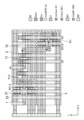
- the embedded signal wiring 71 is used in the signal path connecting the Aout node of the inverter INV_A and the Bin node of the inverter INV_B.
- the embedded signal wiring 71 is arranged at a position overlapping the fin 21 of the inverter INV_A in the Y direction.
- a signal path branching from the M2 wiring N1 to the M2 wiring N2 and the M2 wiring N3 is formed.
- An embedded signal wiring 72 is used in the signal path from the M2 wiring N1 to the M2 wiring N3.
- the embedded signal wiring 72 is arranged at a position overlapping the fin 22 of the inverter INV_A in the Y direction.
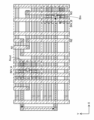
- FIG. 8 is an example of arrangement of signal wirings when embedded signal wirings are not used, in contrast to FIG. As shown in FIG. 8, when the embedded signal wiring is not used, it is necessary to largely detour the signal wiring in the signal path connecting the Aout node of the inverter INV_A and the Bin node of the inverter INV_B (see FIG. 8). arrow). As a result, the wiring density decreases, the area of the semiconductor integrated circuit device increases, the wiring length increases, and the performance of the semiconductor integrated circuit device deteriorates.
- the embedded signal wiring 71 in the embedded signal wiring cell 2 can be used in the signal path connecting the Aout node of the inverter INV_A and the Bin node of the inverter INV_B.
- the embedded signal wiring 72 in the embedded signal wiring cell 2 can be used in the signal path from the M2 wiring N1 to the M2 wiring N3.
- the embedded signal wiring 71 overlaps the fin 21 in the Y direction, and the embedded signal wiring 72 overlaps the fin 22 in the Y direction.
- the wiring density can be improved, and the area of the semiconductor integrated circuit device can be reduced.
- the wiring length can be shortened, the operation speed of the semiconductor integrated circuit device can be increased. In particular, by not providing fins in the embedded signal wiring cell, more embedded signal wiring can be laid, so that the above-described effect is enhanced.
- the transistors included in the standard cells having logic functions are not limited to FinFETs, and may include, for example, nanosheet transistors.
- a nanosheet transistor one or more nanosheets extend in the X direction, and a source and a drain are formed on both sides in the X direction. The nanosheet becomes the channel portion of the nanosheet transistor.
- a large number of embedded signal wirings can be provided in a semiconductor integrated circuit device without causing an increase in area.
Landscapes
- Design And Manufacture Of Integrated Circuits (AREA)
Priority Applications (3)
| Application Number | Priority Date | Filing Date | Title |
|---|---|---|---|
| PCT/JP2021/035637 WO2023053203A1 (ja) | 2021-09-28 | 2021-09-28 | 半導体集積回路装置 |
| JP2023550789A JPWO2023053203A1 (https=) | 2021-09-28 | 2021-09-28 | |
| US18/609,760 US20240234322A1 (en) | 2021-09-28 | 2024-03-19 | Semiconductor integrated circuit device |
Applications Claiming Priority (1)
| Application Number | Priority Date | Filing Date | Title |
|---|---|---|---|
| PCT/JP2021/035637 WO2023053203A1 (ja) | 2021-09-28 | 2021-09-28 | 半導体集積回路装置 |
Related Child Applications (1)
| Application Number | Title | Priority Date | Filing Date |
|---|---|---|---|
| US18/609,760 Continuation US20240234322A1 (en) | 2021-09-28 | 2024-03-19 | Semiconductor integrated circuit device |
Publications (1)
| Publication Number | Publication Date |
|---|---|
| WO2023053203A1 true WO2023053203A1 (ja) | 2023-04-06 |
Family
ID=85781514
Family Applications (1)
| Application Number | Title | Priority Date | Filing Date |
|---|---|---|---|
| PCT/JP2021/035637 Ceased WO2023053203A1 (ja) | 2021-09-28 | 2021-09-28 | 半導体集積回路装置 |
Country Status (3)
| Country | Link |
|---|---|
| US (1) | US20240234322A1 (https=) |
| JP (1) | JPWO2023053203A1 (https=) |
| WO (1) | WO2023053203A1 (https=) |
Families Citing this family (1)
| Publication number | Priority date | Publication date | Assignee | Title |
|---|---|---|---|---|
| JP7640861B2 (ja) * | 2019-10-18 | 2025-03-06 | 株式会社ソシオネクスト | 半導体集積回路装置 |
Citations (3)
| Publication number | Priority date | Publication date | Assignee | Title |
|---|---|---|---|---|
| US20180151494A1 (en) * | 2016-11-28 | 2018-05-31 | Taiwan Semiconductor Manufacturing Co., Ltd. | Semiconductor device having buried metal line and fabrication method of the same |
| WO2021075353A1 (ja) * | 2019-10-18 | 2021-04-22 | 株式会社ソシオネクスト | 半導体集積回路装置 |
| WO2021111604A1 (ja) * | 2019-12-05 | 2021-06-10 | 株式会社ソシオネクスト | 半導体装置 |
Family Cites Families (1)
| Publication number | Priority date | Publication date | Assignee | Title |
|---|---|---|---|---|
| JP2009016683A (ja) * | 2007-07-06 | 2009-01-22 | Panasonic Corp | スタンダードセルを用いた半導体集積回路、及びスタンダードセルライブラリ |
-
2021
- 2021-09-28 JP JP2023550789A patent/JPWO2023053203A1/ja active Pending
- 2021-09-28 WO PCT/JP2021/035637 patent/WO2023053203A1/ja not_active Ceased
-
2024
- 2024-03-19 US US18/609,760 patent/US20240234322A1/en active Pending
Patent Citations (3)
| Publication number | Priority date | Publication date | Assignee | Title |
|---|---|---|---|---|
| US20180151494A1 (en) * | 2016-11-28 | 2018-05-31 | Taiwan Semiconductor Manufacturing Co., Ltd. | Semiconductor device having buried metal line and fabrication method of the same |
| WO2021075353A1 (ja) * | 2019-10-18 | 2021-04-22 | 株式会社ソシオネクスト | 半導体集積回路装置 |
| WO2021111604A1 (ja) * | 2019-12-05 | 2021-06-10 | 株式会社ソシオネクスト | 半導体装置 |
Also Published As
| Publication number | Publication date |
|---|---|
| JPWO2023053203A1 (https=) | 2023-04-06 |
| US20240234322A1 (en) | 2024-07-11 |
Similar Documents
| Publication | Publication Date | Title |
|---|---|---|
| JP7415176B2 (ja) | 半導体集積回路装置 | |
| US20250157929A1 (en) | Semiconductor integrated circuit device | |
| JP7640861B2 (ja) | 半導体集積回路装置 | |
| KR101511436B1 (ko) | 표준 셀을 갖는 집적 회로 | |
| JP7376805B2 (ja) | 半導体集積回路装置 | |
| US10008498B2 (en) | Semiconductor integrated circuit and logic circuit | |
| US20230290779A1 (en) | Integrated circuits having heterogeneous devices therein and methods of designing the same | |
| CN117790467A (zh) | 包括标准单元的集成电路 | |
| WO2023054601A1 (ja) | 半導体装置 | |
| US20240234322A1 (en) | Semiconductor integrated circuit device | |
| WO2023248772A1 (ja) | 半導体集積回路装置 | |
| US20250273567A1 (en) | Semiconductor integrated circuit device | |
| US20240304629A1 (en) | Semiconductor integrated circuit device | |
| CN110326099A (zh) | 半导体集成电路装置 | |
| JP2000223575A (ja) | 半導体装置の設計方法、半導体装置および半導体装置の製造方法 | |
| WO2023132264A1 (ja) | 半導体集積回路装置 | |
| KR20230040391A (ko) | 반도체 장치 및 그 레이아웃 방법 | |
| WO2021192265A1 (ja) | 半導体集積回路装置 | |
| WO2025141944A1 (ja) | 半導体集積回路装置 | |
| US20250096138A1 (en) | Integrated circuit including complementary field effect transistor | |
| JPH11135647A (ja) | 半導体装置 | |
| US20240243117A1 (en) | Integrated circuit including standard cells and method of designing the same | |
| US20240250028A1 (en) | Integrated circuit including backside wiring and method of designing the same | |
| US20250349713A1 (en) | Semiconductor integrated circuit device | |
| WO2025211237A1 (ja) | 半導体集積回路装置 |
Legal Events
| Date | Code | Title | Description |
|---|---|---|---|
| 121 | Ep: the epo has been informed by wipo that ep was designated in this application |
Ref document number: 21959253 Country of ref document: EP Kind code of ref document: A1 |
|
| WWE | Wipo information: entry into national phase |
Ref document number: 2023550789 Country of ref document: JP |
|
| NENP | Non-entry into the national phase |
Ref country code: DE |
|
| 122 | Ep: pct application non-entry in european phase |
Ref document number: 21959253 Country of ref document: EP Kind code of ref document: A1 |