WO2023048105A1 - トランスチップ - Google Patents
トランスチップ Download PDFInfo
- Publication number
- WO2023048105A1 WO2023048105A1 PCT/JP2022/034857 JP2022034857W WO2023048105A1 WO 2023048105 A1 WO2023048105 A1 WO 2023048105A1 JP 2022034857 W JP2022034857 W JP 2022034857W WO 2023048105 A1 WO2023048105 A1 WO 2023048105A1
- Authority
- WO
- WIPO (PCT)
- Prior art keywords
- substrate
- coil
- wiring
- end portion
- wirings
- Prior art date
- Legal status (The legal status is an assumption and is not a legal conclusion. Google has not performed a legal analysis and makes no representation as to the accuracy of the status listed.)
- Ceased
Links
Images









Classifications
-
- H—ELECTRICITY
- H10—SEMICONDUCTOR DEVICES; ELECTRIC SOLID-STATE DEVICES NOT OTHERWISE PROVIDED FOR
- H10D—INORGANIC ELECTRIC SEMICONDUCTOR DEVICES
- H10D86/00—Integrated devices formed in or on insulating or conducting substrates, e.g. formed in silicon-on-insulator [SOI] substrates or on stainless steel or glass substrates
- H10D86/80—Integrated devices formed in or on insulating or conducting substrates, e.g. formed in silicon-on-insulator [SOI] substrates or on stainless steel or glass substrates characterised by multiple passive components, e.g. resistors, capacitors or inductors
- H10D86/85—Integrated devices formed in or on insulating or conducting substrates, e.g. formed in silicon-on-insulator [SOI] substrates or on stainless steel or glass substrates characterised by multiple passive components, e.g. resistors, capacitors or inductors characterised by only passive components
-
- H—ELECTRICITY
- H01—ELECTRIC ELEMENTS
- H01F—MAGNETS; INDUCTANCES; TRANSFORMERS; SELECTION OF MATERIALS FOR THEIR MAGNETIC PROPERTIES
- H01F27/00—Details of transformers or inductances, in general
- H01F27/28—Coils; Windings; Conductive connections
- H01F27/2804—Printed windings
-
- H—ELECTRICITY
- H01—ELECTRIC ELEMENTS
- H01F—MAGNETS; INDUCTANCES; TRANSFORMERS; SELECTION OF MATERIALS FOR THEIR MAGNETIC PROPERTIES
- H01F27/00—Details of transformers or inductances, in general
- H01F27/28—Coils; Windings; Conductive connections
- H01F27/32—Insulating of coils, windings, or parts thereof
- H01F27/323—Insulation between winding turns, between winding layers
-
- H—ELECTRICITY
- H10—SEMICONDUCTOR DEVICES; ELECTRIC SOLID-STATE DEVICES NOT OTHERWISE PROVIDED FOR
- H10D—INORGANIC ELECTRIC SEMICONDUCTOR DEVICES
- H10D84/00—Integrated devices formed in or on semiconductor substrates that comprise only semiconducting layers, e.g. on Si wafers or on GaAs-on-Si wafers
-
- H—ELECTRICITY
- H10—SEMICONDUCTOR DEVICES; ELECTRIC SOLID-STATE DEVICES NOT OTHERWISE PROVIDED FOR
- H10D—INORGANIC ELECTRIC SEMICONDUCTOR DEVICES
- H10D84/00—Integrated devices formed in or on semiconductor substrates that comprise only semiconducting layers, e.g. on Si wafers or on GaAs-on-Si wafers
- H10D84/01—Manufacture or treatment
- H10D84/02—Manufacture or treatment characterised by using material-based technologies
- H10D84/03—Manufacture or treatment characterised by using material-based technologies using Group IV technology, e.g. silicon technology or silicon-carbide [SiC] technology
- H10D84/038—Manufacture or treatment characterised by using material-based technologies using Group IV technology, e.g. silicon technology or silicon-carbide [SiC] technology using silicon technology, e.g. SiGe
-
- H—ELECTRICITY
- H01—ELECTRIC ELEMENTS
- H01F—MAGNETS; INDUCTANCES; TRANSFORMERS; SELECTION OF MATERIALS FOR THEIR MAGNETIC PROPERTIES
- H01F27/00—Details of transformers or inductances, in general
- H01F27/28—Coils; Windings; Conductive connections
- H01F27/2804—Printed windings
- H01F2027/2809—Printed windings on stacked layers
-
- H—ELECTRICITY
- H01—ELECTRIC ELEMENTS
- H01F—MAGNETS; INDUCTANCES; TRANSFORMERS; SELECTION OF MATERIALS FOR THEIR MAGNETIC PROPERTIES
- H01F27/00—Details of transformers or inductances, in general
- H01F27/28—Coils; Windings; Conductive connections
- H01F27/32—Insulating of coils, windings, or parts thereof
- H01F27/327—Encapsulating or impregnating
Definitions
- This disclosure relates to a transformer chip.
- Patent Literature 1 discloses a transformer chip that includes two coils arranged facing each other with a space therebetween in the vertical direction.
- the characteristics of the transformer chip are determined by the configuration and arrangement of the two coils.
- the dielectric strength of a transformer chip is determined by the distance between two coils. If the dielectric strength is to be changed, the distance between the two coils must be changed according to the thickness of the insulating film, the number of layers, etc., so the manufacturing process of the transformer chip needs to be changed, which is time-consuming. Therefore, there is room for improvement in the device design of transformer chips.
- a transformer chip that is one aspect of the present disclosure includes a substrate having a substrate main surface, a first coil provided on the substrate main surface, and a coil separated from the first coil on the substrate main surface in a first direction. and a second coil provided at a position, wherein the first coil is provided on the main surface of the substrate, extends along a direction intersecting with the first direction, and includes a plurality of coils arranged in the first direction. a first substrate wiring; and a plurality of first connection wirings arranged in the first direction and respectively connected between two of the first substrate wirings adjacent in the first direction; A coil is provided on the main surface of the substrate, extends along a direction intersecting the first direction, and is arranged in the first direction. and a plurality of second connection wirings respectively connected between two of the second substrate wirings adjacent in one direction.
- FIG. 1 is a perspective view of the transformer chip of the first embodiment.
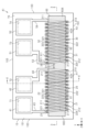
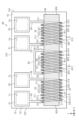
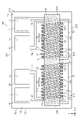
- 2 is a plan view of the transformer chip of FIG. 1.
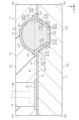
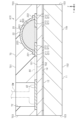
- FIG. 3 is a cross-sectional view taken along line 3-3 of FIG. 2.
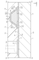
- FIG. 4 is a cross-sectional view taken along line 4-4 of FIG. 2.
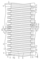
- FIG. 5 is a plan view showing the first coil.
- FIG. 6 is a plan view showing the second coil.
- FIG. 7 is a circuit diagram showing an application example of the transformer chip.
- FIG. 8 is a perspective view of the transformer chip of the second embodiment.
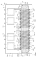
- 9 is a plan view of the transformer chip of FIG. 8.
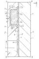
- FIG. 10 is a cross-sectional view taken along line 10-10 of FIG. 9.
- FIG. 11 is a cross-sectional view taken along line 11-11 of FIG. 9.
- FIG. FIG. 10 is a cross-sectional view taken along line 10-10 of FIG. 9.
- FIG. 11 is a cross-sectional view taken along line 11-11 of FIG. 9.
- FIG. 12 is a perspective view of the transformer chip of the third embodiment.
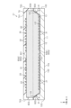
- 13 is a plan view of the transformer chip of FIG. 12.
- FIG. 14 is a cross-sectional view taken along line 14-14 of FIG. 13.
- FIG. 15 is a cross-sectional view taken along line 15-15 of FIG. 13.
- FIG. 16 is a cross-sectional view of a modified transformer chip.
- FIG. 17 is a cross-sectional view of a modified transformer chip.
- FIG. 18 is a plan view of a modified transformer chip.
- FIG. 19 is a plan view of a modified transformer chip.
- FIG. 20 is a plan view of a modified transformer chip.
- FIG. 21 is a plan view of a modified transformer chip.
- FIG. 22 is a plan view of a modified transformer chip.
- FIG. 23 is a plan view of a modified transformer chip.
- FIG. 24 is a cross-sectional view of a modified transformer chip.
- FIG. 1 is a perspective view of the transformer chip A1.
- FIG. 2 is a plan view of the transformer chip A1.
- 3 is a cross-sectional view taken along line 3-3 of FIG. 2.
- FIG. 4 is a cross-sectional view taken along line 4-4 of FIG. 2.
- FIG. 5 is an enlarged plan view showing the first coil 20.
- FIG. 6 is an enlarged plan view showing the second coil 30.
- FIG. 7 is a circuit diagram showing an application example of the transformer chip A1.
- the transformer chip A1 has a substrate 10, a first coil 20, a second coil 30, input pads 41 and 42, output pads 51 and 52, an insulating member 60 and a sealing resin 70. are doing.
- the substrate 10 is formed in a substantially flat plate shape.
- the thickness direction of the substrate 10 is defined as the Z direction.
- the first direction and the second direction that are orthogonal to each other are defined as the X direction and the Y direction, respectively.
- the substrate 10 is formed in a rectangular shape with long sides in the X direction and short sides in the Y direction when viewed from the Z direction.
- the substrate 10 has a substrate main surface 101 , a substrate back surface 102 and a plurality of substrate side surfaces 103 .
- the substrate main surface 101 and the substrate back surface 102 face opposite sides in the Z direction.
- the substrate main surface 101 and the substrate back surface 102 are flat surfaces.
- the plurality of substrate side surfaces 103 face either the X direction or the Y direction.
- the plurality of substrate side surfaces 103 are surfaces sandwiched between the substrate main surface 101 and the substrate back surface 102 .
- the substrate 10 of this embodiment is composed of a substrate body 11 and an insulating film 12 .
- the substrate body 11 is configured by, for example, a semiconductor substrate.
- the insulating film 12 is a film having electrical insulation. Note that the substrate 10 may be made of an insulating resin.
- the substrate main body 11 of this embodiment is a substrate formed from a material containing Si (silicon).
- a wide bandgap semiconductor or a compound semiconductor may be used as a semiconductor substrate for the substrate 10 .
- the wide bandgap semiconductor may be SiC (silicon carbide).
- the compound semiconductor may be a III-V compound semiconductor.
- the compound semiconductor may contain at least one of AlN (aluminum nitride), InN (indium nitride), GaN (gallium nitride), and GaAs (gallium arsenide).
- the substrate main body 11 may be an insulating substrate made of a material containing glass instead of the semiconductor substrate. Further, as the substrate main body 11, a substrate made of a synthetic resin whose main material is an epoxy resin or the like may be used.
- Insulating film 12 is made of, for example, SiO 2 (silicon oxide). This insulating film 12 is formed by thermally oxidizing the substrate body 11, which is, for example, a Si substrate.
- the material and formation method of the insulating film 12 are not limited.
- insulating film 12 may be made of a material containing SiO 2 and resin.
- the insulating film 12 may be made of SiN (silicon nitride), AiN (aluminum nitride), or the like.
- the insulating film 12 may be made of resin.
- the substrate 10 includes the substrate body 11 and the insulating film 12.
- the substrate 10 has a substrate main surface 101 , a substrate back surface 102 and a plurality of substrate side surfaces 103 .
- the substrate main surface 101 is composed of the surface of the insulating film 12 .
- the substrate back surface 102 is configured by the back surface of the substrate body 11 .
- the substrate side surface 103 is composed of the side surface of the substrate body 11 and the side surface of the insulating film 12 .
- the first coil 20 and the second coil 30 are arranged on the substrate main surface 101 of the substrate 10 .
- the first coil 20 and the second coil 30 are arranged along the substrate main surface 101 on the substrate main surface 101 .
- the first coil 20 and the second coil 30 are arranged side by side in the X direction on the main surface 101 of the substrate.
- the first coil 20 has a plurality of first substrate wirings 21 and a plurality of first connection wirings 22 .
- the first substrate wiring 21 and the first connection wiring 22 are made of a conductive metal such as Cu (copper), Cu alloy, or the like.
- the plurality of first substrate wirings 21 are provided on the substrate main surface 101 of the substrate 10 . As shown in FIG. 2, the plurality of first substrate wirings 21 are arranged along the X direction in which the first coils 20 and the second coils 30 are arranged. A plurality of first substrate wirings 21 are formed to extend along a direction crossing the X direction.
- each of the plurality of first substrate wirings 21 has a first end portion 211, a second end portion 212 opposite to the first end portion 211, and a first end portion 212. It has a first conductor portion 213 between the end portion 211 and the second end portion 212 .
- the first end portion 211 and the second end portion 212 are formed in a rectangular shape that is long in the Y direction with respect to the X direction when viewed from the Z direction.
- the first end portions 211 of the first substrate wirings 21 are arranged to be shifted in the X direction (rightward in FIG. 5) with respect to the second end portions 212 when viewed from the Z direction.
- the first end 211 of each first substrate wiring 21 is aligned with the second end 212 of the first substrate wiring 21 and each first substrate wiring 21 in the X direction. It is arranged between the second ends 212 of the adjacent first substrate wirings 21 .
- the first conductor portion 213 connects the first end portion 211 and the second end portion 212 . Therefore, the first conductor portion 213 of each first substrate wiring 21 extends at a predetermined angle with respect to the Y direction when viewed from the Z direction. As shown in FIG. 2 , the first conductor portion 213 is inclined toward the second coil 30 from the second end portion 212 toward the first end portion 211 when viewed in the Z direction. In other words, the first conductor portion 213 is inclined away from the second coil 30 from the first end portion 211 toward the second end portion 212 when viewed in the Z direction.
- the first coil 20 has a first connecting portion 23 at the end opposite to the second coil 30 .
- the first connection portion 23 is formed in a rectangular shape that is longer in the Y direction than in the X direction, like the first end portion 211 of the first substrate wiring 21 .
- the first connecting portion 23 is arranged at the same position as the first end portion 211 of each first substrate wiring 21 in the Y direction when viewed from the Z direction.
- the first connecting portion 23 is arranged at a position where the distance between the first end portions 211 adjacent in the X direction is equal to the distance between the first end portions 211 in the X direction when viewed from the Z direction.
- the insulating member 60 is formed so as to pass through the first coil 20 and the second coil 30. As shown in FIGS. That is, the insulating member 60 has a first end portion 603 that protrudes toward the side opposite to the second coil 30 in the first coil 20, and a portion that protrudes toward the side opposite to the first coil 20 in the second coil 30. and a second end 604 .
- Insulating member 60 is made of, for example, phenol resin, polyimide resin, or the like.
- the insulating member 60 has a first portion 61 corresponding to the first coil 20 and a second portion 62 corresponding to the second coil 30 .
- the first portion 61 is a portion arranged between the first substrate wiring 21 and the first connection wiring 22 of the first coil 20 .
- the second portion 62 is a portion arranged between the second substrate wiring 31 and the second connection wiring 32 of the second coil 30 .
- the insulating member 60 is formed so as to cover the first substrate wiring 21. As shown in FIG. Specifically, as shown in FIGS. 2, 4, and 5, the insulating member 60 is formed to expose the first end portion 211 and the second end portion 212 and cover the first conductor portion 213. As shown in FIGS. As shown in FIGS. 3 and 4 , the insulating member 60 is in contact with the main surface 101 of the substrate and is formed so as to cover the first conductor portion 213 of the first substrate wiring 21 . As shown in FIG. 3 , the insulating member 60 is in contact with the upper and side surfaces of the first conductor portion 213 .
- the insulating member 60 is formed so as to be in contact with the substrate main surface 101 in the Z direction and swell in the direction away from the substrate main surface 101 .
- the insulating member 60 has a cross-sectional shape in a plane (YZ plane) orthogonal to the X direction, which is arcuate and bulges in a direction away from the main surface 101 of the substrate.
- the insulating member 60 is formed in a strip shape extending in the X direction.
- the plurality of first connection wirings 22 are arranged along the X direction in which the first coils 20 and the second coils 30 are arranged.
- the plurality of first connection wirings 22 are formed to extend along a direction crossing the X direction.
- the first connection wiring 22 is in contact with the insulating member 60 and is formed so as to extend along the surface of the insulating member 60 having an arcuate cross-sectional shape in a plane perpendicular to the X direction.
- the first connection wiring 22 is formed so that the central portion thereof is separated from the first substrate wiring 21 by the insulating member 60 in the Z direction.
- Each of the plurality of first connection wirings 22 has a first end portion 211 of one first substrate wiring 21 and a second end portion 212 of the other first substrate wiring 21 of two first substrate wirings 21 adjacent to each other in the X direction. is formed to connect the
- each of the plurality of first connection wirings 22 has a third end portion 221, a fourth end portion 222 opposite to the third end portion 221, and a third end portion 222. It has a second conductor portion 223 between the end portion 221 and the fourth end portion 222 .
- the third end portion 221 and the fourth end portion 222 are formed in a rectangular shape that is long in the Y direction with respect to the X direction when viewed from the Z direction.
- the third end portions 221 of the first connection wirings 22 are arranged shifted in the X direction (rightward in FIG. 5) with respect to the fourth end portions 222 when viewed from the Z direction.
- the third end 221 of each first connection wiring 22 is aligned with the fourth end 222 of the first connection wiring 22 and each first connection wiring 22 in the X direction. It is arranged between the fourth ends 222 of the adjacent first connection wirings 22 .
- the third end 221 of the first connection wiring 22 is connected to the first end 211 of the first substrate wiring 21 .
- the fourth end 222 of the first connection wiring 22 is connected to the second end 212 of the first substrate wiring 21 adjacent to the first substrate wiring 21 to which the third end 221 is connected. That is, the plurality of first connection wirings 22 are connected between two first substrate wirings 21 adjacent in the X direction.
- the second conductor portion 223 connects the third end portion 221 and the fourth end portion 222 . Therefore, the second conductor portion 223 of each first connection wiring 22 extends at a predetermined angle with respect to the Y direction when viewed from the Z direction. As shown in FIG. 2 , the second conductor portion 223 is inclined away from the second coil 30 from the fourth end portion 222 toward the third end portion 221 when viewed in the Z direction. In other words, the second conductor portion 223 is inclined toward the second coil 30 from the third end portion 221 toward the fourth end portion 222 when viewed in the Z direction.
- the first connection wiring 22 is not connected to the first end portion 211 of the first substrate wiring 21X located at the end near the second coil 30 .
- the third end 221 of the first connection wiring 22X located at the end opposite to the second coil 30 is connected to the first connection portion 23 of the first coil 20. It is connected.
- the width of the first connection wiring 22 is formed narrower than the width of the first substrate wiring 21 .
- the first board wiring 21 has the first end portion 211 , the second end portion 212 and the first conductor portion 213 .
- the first end portion 211 and the second end portion 212 are formed in a rectangular shape that is long in the Y direction with respect to the X direction when viewed from the Z direction.
- the first connection wiring 22 has a third end portion 221 , a fourth end portion 222 and a second conductor portion 223 .
- the third end portion 221 and the fourth end portion 222 are formed in a rectangular shape that is long in the Y direction with respect to the X direction when viewed from the Z direction.
- the width W13 of the third end portion 221 is narrower than the width W11 of the first end portion 211.
- the length L13 of the third end portion 221 is shorter than the length L11 of the first end portion 211 .
- the width W14 of the fourth end 222 is narrower than the width W12 of the second end 212 .
- the length L14 of the fourth end 222 is shorter than the length L12 of the second end 212 .
- the width W11 of the first end 211 in the X direction is equal to the width W12 of the second end 212 in the X direction.
- the length L11 of the first end 211 in the Y direction is equal to the length L12 of the second end 212 in the Y direction.
- the width W13 of the third end portion 221 in the X direction is equal to the width W14 of the fourth end portion 222 in the X direction.
- the length L13 of the third end portion 221 in the Y direction is equal to the length L14 of the fourth end portion 222 in the Y direction.
- equal width and length include differences within the range of manufacturing error.
- the width of the first conductor portion 213 in the X direction is equal to the width of the first end portion 211 and the second end portion 212 .
- the width of the second conductor portion 223 in the X direction is equal to the width of the third end portion 221 and the fourth end portion 222 .
- the width of the first conductor portion 213 may be different from the widths of the first end portion 211 and the second end portion 212 .
- the width of the second conductor portion 223 may be different from the width of the third end portion 221 and the fourth end portion 222 .
- the second coil 30 has a plurality of second substrate wirings 31 and a plurality of second connection wirings 32.
- the second substrate wiring 31 and the second connection wiring 32 are made of a conductive metal such as Cu (copper), Cu alloy, or the like.
- the plurality of second substrate wirings 31 are provided on the substrate main surface 101 of the substrate 10 . As shown in FIG. 2, the plurality of second substrate wirings 31 are arranged along the X direction in which the first coils 20 and the second coils 30 are arranged. A plurality of second substrate wirings 31 are formed to extend along a direction crossing the X direction.
- each of the plurality of second substrate wirings 31 has a first end portion 311, a second end portion 312 opposite to the first end portion 311, and a first end portion 312. It has a first conductor portion 313 between the end portion 311 and the second end portion 312 .
- the first end portion 311 and the second end portion 312 are formed in a rectangular shape that is longer in the Y direction than in the X direction when viewed from the Z direction.
- the first ends 311 of the second substrate wirings 31 are arranged to be displaced in the X direction (to the right in FIG. 6) with respect to the second ends 312 when viewed from the Z direction.
- the first end 311 of each second substrate wiring 31 is aligned with the second end 312 of the second substrate wiring 31 and each second substrate wiring 31 in the X direction. It is arranged between the second ends 312 of the adjacent second substrate wirings 31 .
- the first conductor portion 313 connects the first end portion 311 and the second end portion 312 . Therefore, the first conductor portion 313 of each second substrate wiring 31 extends at a predetermined angle with respect to the Y direction when viewed from the Z direction. As shown in FIG. 2 , the first conductor portion 313 is inclined away from the first coil 20 from the second end portion 312 toward the first end portion 311 when viewed in the Z direction. In other words, the first conductor portion 313 is inclined toward the first coil 20 from the first end portion 311 toward the second end portion 312 when viewed in the Z direction.
- the second coil 30 has a second connecting portion 33 at the end on the first coil 20 side.
- the second connection portion 33 is formed in a rectangular shape that is longer in the Y direction than in the X direction.
- the second connection portion 33 is arranged at the same position as the first end portion 311 of each second substrate wiring 31 in the Y direction when viewed from the Z direction.
- the second connecting portion 33 is arranged at a position where the distance between the first end portions 311 adjacent to each other in the X direction is equal to the distance between the first end portions 311 in the X direction when viewed from the Z direction.
- the insulating member 60 is formed so as to cover the second board wiring 31. As shown in FIGS. Specifically, as shown in FIGS. 2 and 6, the insulating member 60 is formed to expose the first end portion 311 and the second end portion 312 and cover the first conductor portion 313 . As shown in FIG. 3 , the insulating member 60 is in contact with the substrate main surface 101 and is formed so as to cover the first conductor portion 313 of the second substrate wiring 31 . As shown in FIG. 3 , the insulating member 60 is in contact with the top and side surfaces of the first conductor portion 313 .
- the plurality of second connection wirings 32 are arranged along the X direction in which the first coils 20 and the second coils 30 are arranged.
- a plurality of second connection wirings 32 are formed to extend along a direction crossing the X direction.
- the second connection wiring 32 like the first connection wiring 22 of the first coil 20 shown in FIG. formed to extend along the The second connection wiring 32 is formed so that the central portion thereof is separated from the second substrate wiring 31 by the insulating member 60 in the Z direction.
- Each of the plurality of second connection wirings 32 has a first end portion 311 of one second substrate wiring 31 and a second end portion 312 of the other second substrate wiring 31 of two second substrate wirings 31 adjacent to each other in the X direction. is formed to connect the
- each of the plurality of second connection wirings 32 has a third end portion 321, a fourth end portion 322 opposite to the third end portion 321, and a third end portion 322. It has a second conductor portion 323 between the end portion 321 and the fourth end portion 322 .
- the third end portion 321 and the fourth end portion 322 are formed in a rectangular shape that is long in the Y direction with respect to the X direction when viewed from the Z direction.
- the third end portions 321 of the second connection wirings 32 are arranged to be shifted in the X direction (rightward in FIG. 6) with respect to the fourth end portions 322 when viewed from the Z direction.
- the third end 321 of each second connection wiring 32 is aligned with the fourth end 322 of the second connection wiring 32 and each second connection wiring 32 in the X direction. It is arranged between the fourth ends 322 of the adjacent second connection wirings 32 .
- the third end 321 of the second connection wiring 32 is connected to the first end 311 of the second substrate wiring 31 .
- the fourth end 322 of the second connection wiring 32 is connected to the second end 312 of the second substrate wiring 31 adjacent to the second substrate wiring 31 to which the third end 321 is connected. That is, the plurality of second connection wirings 32 are connected between two second substrate wirings 31 adjacent in the X direction.
- the second conductor portion 323 connects the third end portion 321 and the fourth end portion 322 . Therefore, the second conductor portion 323 of each second substrate wiring 31 extends at a predetermined angle with respect to the Y direction when viewed from the Z direction. As shown in FIG. 2 , the second conductor portion 323 is inclined toward the first coil 20 from the fourth end portion 322 toward the third end portion 321 when viewed in the Z direction. In other words, the second conductor portion 323 is inclined away from the first coil 20 from the third end portion 321 toward the fourth end portion 322 when viewed in the Z direction.
- the second connection wiring 32 is not connected to the first end portion 311 of the second substrate wiring 31X located at the end opposite to the first coil 20 in the second substrate wiring 31 of the present embodiment.
- the third end portion 321 of the second connection wiring 32X located at the end near the first coil 20 is connected to the second connection portion 33 of the second coil 30.
- the width of the second connection wiring 32 is formed narrower than the width of the second substrate wiring 31 .
- the second substrate wiring 31 has the first end portion 311 , the second end portion 312 and the first conductor portion 313 .
- the first end portion 311 and the second end portion 312 are formed in a rectangular shape that is longer in the Y direction than in the X direction when viewed from the Z direction.
- the second connection wiring 32 has a third end portion 321 , a fourth end portion 322 and a second conductor portion 323 .
- the third end portion 321 and the fourth end portion 322 are formed in a rectangular shape that is long in the Y direction with respect to the X direction when viewed from the Z direction.
- the width W23 of the third end portion 321 is narrower than the width W21 of the first end portion 311.
- the length L23 of the third end 321 is shorter than the length L21 of the first end 311 .
- width W24 of fourth end 322 is narrower than width W22 of second end 312 .
- the length L24 of the fourth end 322 is shorter than the length L22 of the second end 312 .
- the width W21 of the first end 311 in the X direction is equal to the width W22 of the second end 312 in the X direction.
- the length L21 of the first end portion 311 in the Y direction is equal to the length L22 of the second end portion 312 in the Y direction.
- the width W23 of the third end portion 321 in the X direction is equal to the width W24 of the fourth end portion 322 in the X direction.
- the length L23 of the third end portion 321 in the Y direction is equal to the length L24 of the fourth end portion 322 in the Y direction.
- the width of the first conductor portion 313 in the X direction is equal to the width of the first end portion 311 and the second end portion 312 .
- the width of the second conductor portion 323 in the X direction is equal to the width of the third end portion 321 and the fourth end portion 322 .
- the width of the first conductor portion 313 may be different from the widths of the first end portion 311 and the second end portion 312 .
- the width of the second conductor portion 323 may be different from the width of the third end portion 321 and the fourth end portion 322 .
- the first coil 20 and the second coil 30 are arranged with a predetermined distance D1.
- This distance D1 is the distance between the coils.
- the inter-coil distance may be defined by, for example, the distance between the first substrate wiring 21 and the second substrate wiring 31 and the distance between the first connection wiring 22 and the second connection wiring 32 .
- the inter-coil distance D ⁇ b>1 is set wider than the wiring interval P ⁇ b>1 of the first coils 20 .
- the wiring spacing P1 is defined as the spacing between two first substrate wirings 21 adjacent in the X direction.
- the inter-coil distance D1 is set wider than the wiring interval P2 of the second coils 30 .
- the wiring spacing P2 is defined as the spacing between two second substrate wirings 31 adjacent in the X direction.
- the wiring interval P1 of the first coil 20 and the wiring interval P2 of the second coil 30 are the same. Note that the wiring interval P1 between the first coils 20 and the wiring interval P2 between the second coils 30 may be different.
- the transformer chip A1 has input pads 41 and 42 and output pads 51 and 52 .
- the input pads 41 and 42 and the output pads 51 and 52 are formed in a rectangular shape when viewed from the Z direction.
- Input pads 41 and 42 and output pads 51 and 52 are configured to be connectable with bonding wires.
- the bonding wire BW connected to the input pad 42 is indicated by a chain double-dashed line. Bonding wires are connected to input pad 41 and output pads 51 and 52 shown in FIGS. 1 and 2 as well as input pad 42 .
- the input pads 41 and 42 are connected to the first coil 20. Specifically, the input pad 41 is connected to the first connection portion 23 of the first coil 20 by a pad connection wiring 43 .
- the input pad 42 is connected to the first end portion 211 of the first substrate wiring 21X of the first coil 20 by the pad connection wiring 44 .
- Input pads 41 and 42 and pad connection wirings 43 and 44 are made of a conductive metal such as Cu, Cu alloy, or the like.
- the output pads 51 and 52 are connected to the second coil 30. Specifically, the output pad 51 is connected to the second connection portion 33 of the second coil 30 by a pad connection wiring 53 .
- the output pad 52 is connected to the first end portion 311 of the second substrate wiring 31X of the second coil 30 by the pad connection wiring 54 .
- the output pads 51, 52 and the pad connection wirings 53, 54 are made of a conductive metal such as Cu, Cu alloy, or the like.
- the transformer chip A1 has a sealing resin 70.
- the sealing resin 70 is formed to have the same size as the substrate 10 when viewed from the Z direction.
- the sealing resin 70 has a resin main surface 701 , a resin back surface 702 and a plurality of resin side surfaces 703 .
- the resin main surface 701 and the resin back surface 702 face opposite sides in the Z direction.
- the resin main surface 701 faces the same direction as the substrate main surface 101 of the substrate 10 .
- the plurality of resin side surfaces 703 face either the X direction or the Y direction.
- the sealing resin 70 seals the first coil 20 and the second coil 30 .
- the sealing resin 70 has openings 71 and 72 that partially expose the input pads 41 and 42 .
- the sealing resin 70 has openings 73 and 74 that partially expose the output pads 51 and 52 .
- Sealing resin 70 is made of, for example, phenol resin, polyimide resin, or the like.
- the bonding wire BW is connected to the portion of the input pad 42 exposed from the opening 72 of the sealing resin 70 .
- bonding wires are connected to the portions of the sealing resin 70 exposed through the openings 71, 73 and 74 of the input pad 41 and the output pads 51 and 52 shown in FIGS.
- the transformer chip A1 of this embodiment can be used to insulate between inputs and outputs in various circuits.
- FIG. 7 shows an example of a circuit to which the transformer chip A1 of this embodiment is applied.
- This circuit applies a drive voltage signal to the gate of the switching element 91 .
- Switching element 91 configures inverter device 90 by being connected in series with switching element 92 .
- This inverter device 90 is mounted in, for example, an electric vehicle or a hybrid vehicle.
- the switching element 91 is, for example, a high-side switching element connected to a drive power supply.
- the switching element 92 is a low-side switching element.
- switching elements 91 and 92 include transistors such as SiMOSFETs (Si Metal-Oxide-Semiconductor Field-Effect Transistors), SiCMOSFETs, and IGBTs (Insulated Gate Bipolar Transistors). In the following description, it is assumed that the switching elements 91 and 92 are SiCMOSFETs.
- Transformer chip A 1 is connected between low voltage circuit 94 and high voltage circuit 95 .
- the low voltage circuit 94 is connected to a control circuit (ECU: Electronic Control Unit) 93 that controls the switching elements 91 and 92 .
- the low voltage circuit 94 is connected to the high voltage circuit 95 via the transformer chip A1.
- the low voltage circuit 94 is configured to operate with the first voltage V1.
- the high voltage circuit 95 is configured to operate with a second voltage V2 higher than the first voltage V1.
- the first voltage V1 and the second voltage V2 are DC voltages.
- the ground GND1 of the low-voltage circuit 94 and the ground GND2 of the high-voltage circuit 95 are provided independently.
- the potential of the ground GND1 of the low-voltage circuit 94 is set as a first reference potential, and the potential of the ground GND2 of the high-voltage circuit 95 is set as a second reference potential.
- the first voltage V1 is the voltage from the first reference potential
- the second voltage V2 is the voltage from the second reference potential.
- This circuit is configured such that a signal is transmitted from the low voltage circuit 94 to the high voltage circuit 95 through the transformer chip A1 based on a control signal from the ECU 93, and a drive voltage signal is output from the high voltage circuit 95.
- a signal transmitted from the low-voltage circuit 94 to the high-voltage circuit 95, that is, a signal output from the low-voltage circuit 94 is a signal for driving the switching element 91, for example.
- This signal is, for example, a pulse signal.
- the high voltage circuit 95 generates a signal for driving the switching element 91 based on the signal received from the low voltage circuit 94 through the transformer chip A1 and applies the signal to the switching element 91 .
- Switching element 91 is turned on and off in response to a signal applied by high voltage circuit 95 .
- the transformer chip A1 is insulated between the first coil 20 and the second coil 30. Therefore, the transformer chip A1 provides isolation between the low voltage circuit 94 and the high voltage circuit 95. FIG. That is, the transformer chip A1 cuts off the transmission of the DC voltage between the low voltage circuit 94 and the high voltage circuit 95. FIG. On the other hand, the transformer chip A1 is configured to be able to transmit signals such as pulse signals between the low voltage circuit 94 and the high voltage circuit 95 .
- the first coil 20 of the transformer chip A1 is connected to the ground GND1 of the low voltage circuit 94.
- the second coil 30 of the transformer chip A1 is connected to the ground GND2 of the high voltage circuit 95.
- a ground GND2 of the high voltage circuit 95 is connected to the source terminal of the switching element 91 driven by the high voltage circuit 95 . Therefore, the potential at one terminal of the second coil 30 becomes the second reference potential.
- This second reference potential varies as the inverter device 90 is driven.
- the first coil 20 is connected to the ground GND1 of the first reference potential. Therefore, between the first coil 20 and the second coil 30, a dielectric strength corresponding to the fluctuating second reference potential is required.
- the transformer chip A1 of this embodiment has a first coil 20 and a second coil 30 provided on the substrate main surface 101 of the substrate 10 .
- the first coil 20 and the second coil 30 are arranged side by side on the substrate main surface 101 of the substrate 10 along the first direction.
- the first coil 20 has a plurality of first substrate wirings 21 and a plurality of first connection wirings 22 arranged in the X direction.
- the plurality of first substrate wirings 21 extends along a direction crossing the X direction.
- a plurality of first connection wirings 22 are connected between two first substrate wirings 21 adjacent to each other in the X direction.
- the second coil 30 has a plurality of second substrate wirings 31 and a plurality of second connection wirings 32 arranged in the X direction.
- a plurality of second substrate wirings 31 extend along a direction crossing the X direction.
- a plurality of second connection wirings 32 are connected between two second substrate wirings 31 adjacent to each other in the X direction.
- the position of the first coil 20 is defined by the positions of the first substrate wiring 21 and the first connection wiring 22 formed on the substrate main surface 101 of the substrate 10 .
- the position of the second coil 30 is defined by the positions of the second substrate wiring 31 and the second connection wiring 32 formed on the substrate main surface 101 of the substrate 10 .
- the dielectric strength of the transformer chip A1 is determined by the distance between the first coil 20 and the second coil 30. FIG. In other words, the dielectric strength of the transformer chip A1 is determined by the arrangement positions of the first coil 20 and the second coil 30 . Therefore, a transformer chip A1 having desired characteristics can be easily obtained. That is, the degree of freedom in designing the transformer chip A1 can be improved.
- the withstand voltage of the transformer chip A1 can be adjusted. Therefore, in the manufacturing process, the characteristics of the transformer chip A1 can be easily changed without changing the steps such as adding a new step. Therefore, the degree of freedom in designing the transformer chip A1 can be improved.
- the first coil 20 and the second coil 30 are formed by plating. Specifically, a mask having openings corresponding to the first substrate wiring 21 of the first coil 20 and the second substrate wiring 31 of the second coil 30 is formed, and plating metal is deposited in the openings of the mask.
- the mask is formed, for example, by exposing and developing a resist layer having photosensitivity. Therefore, the positions of the first coil 20 and the second coil 30 can be changed only by changing the positions of the openings in the mask. Therefore, the degree of freedom in designing the transformer chip A1 can be improved.
- the first connection wirings 22 and the first substrate wirings 21 are alternately connected along the X direction.
- One first connection wiring 22 and one first substrate wiring 21 constitute one coil portion (one turn) in the first coil 20 . That is, one first connection wiring 22 and one first board wiring 21 constitute a unit element of one turn of the first coil 20 . Therefore, the number of first substrate wirings 21 and the number of first connection wirings 22 correspond to the number of turns of the first coil 20 . Therefore, the number of turns of the first coil 20 can be easily changed by changing the number of the first substrate wirings 21 and the first connection wirings 22 formed on the substrate 10 . Therefore, the degree of freedom in designing the first coil 20 can be improved.
- the first substrate wiring 21 extends in a direction crossing the X direction.
- the first substrate wiring 21 and the first connection wiring 22 form one coil portion (one turn) of the first coil 20 .
- the length of one turn is determined by the length of the first substrate wiring 21 and the length of the first connection wiring 22 .
- the first substrate wiring 21 is formed on the substrate main surface 101 . Therefore, the length of the first substrate wiring 21 can be easily changed. Therefore, the degree of freedom in designing the first coil 20 can be improved.
- the second connection wiring 32 and the second substrate wiring 31 are alternately connected along the X direction.
- One second connection wiring 32 and one second substrate wiring 31 constitute one coil portion (one turn) of the second coil 30 . That is, one second connection wiring 32 and one second board wiring 31 constitute a unit element of one turn of the second coil 30 . Therefore, the number of second substrate wirings 31 and the number of second connection wirings 32 correspond to the number of turns of the second coil 30 . Therefore, the number of turns of the second coil 30 can be easily changed by changing the number of the second substrate wirings 31 and the second connection wirings 32 formed on the substrate 10 . Therefore, the degree of freedom in designing the second coil 30 can be improved.
- the third end 221 of the first connection wiring 22 is connected to the first end 211 of the first substrate wiring 21, and the fourth end 222 of the first connection wiring 22 is connected to , and the second end portion 212 of the first substrate wiring 21 .
- the length of the first connection wiring 22 can be easily changed according to the length of the first substrate wiring 21 . Therefore, the degree of freedom in designing the first coil 20 can be improved.
- the first connection wiring 22 is formed along the surface 601 of the insulating member 60. As shown in FIG. Therefore, the length of the first connection wiring 22 is defined by the cross-sectional shape of the insulating member 60 and the height of the insulating member 60 . Therefore, the length of the first connection wiring 22 can be easily changed according to the shape of the insulating member 60 . Therefore, the degree of freedom in designing the first coil 20 can be improved.
- the second connection wiring 32 is formed along the surface 601 of the insulating member 60. As shown in FIG. Therefore, the length of the second connection wiring 32 is defined by the cross-sectional shape of the insulating member 60 and the height of the insulating member 60 . Therefore, the length of the second connection wiring 32 can be easily changed according to the shape of the insulating member 60 . Therefore, the degree of freedom in designing the second coil 30 can be improved.
- the length of one turn in the first coil 20 is determined by the lengths of the first substrate wiring 21 and the first connection wiring 22 . As shown in FIG. 4 , the length of one turn of the first coil 20 is determined by the cross-sectional shape of the insulating member 60 when viewed from the X direction. That is, by changing the size of the insulating member 60, the length of one turn of the first coil 20 can be easily changed. The length of one turn of the second coil 30 can also be easily changed in the same manner as the first coil 20 . That is, in the transformer chip A1, the degree of freedom in designing the length of one turn of the first coil 20 and the second coil 30 can be improved.
- the width W13 of the third end portion 221 is narrower than the width W11 of the first end portion 211. Therefore, even if the formation position of the third end portion 221 is displaced in the X direction due to a manufacturing error, the third end portion 221 can be formed on the first end portion 211 . Also, the length L13 of the third end portion 221 is shorter than the length L11 of the first end portion 211 . Therefore, even if the formation position of the third end portion 221 is displaced in the Y direction due to a manufacturing error, the third end portion 221 can be formed on the first end portion 211 .
- the width W14 of the fourth end portion 222 is narrower than the width W12 of the second end portion 212. Therefore, even if the formation position of the fourth end portion 222 is displaced in the X direction due to manufacturing errors, the fourth end portion 222 can be formed on the second end portion 212 .
- the length L14 of the fourth end 222 is shorter than the length L12 of the second end 212 . Therefore, even if the formation position of the fourth end portion 222 is displaced in the Y direction due to a manufacturing error, the fourth end portion 222 can be formed on the second end portion 212 .
- the width W23 of the third end portion 321 is narrower than the width W21 of the first end portion 311. Therefore, even if the formation position of the third end portion 321 is displaced in the X direction due to a manufacturing error, the third end portion 321 can be formed on the first end portion 311 . Also, the length L23 of the third end portion 321 is shorter than the length L21 of the first end portion 311 . Therefore, even if the formation position of the third end portion 321 is displaced in the Y direction due to a manufacturing error, the third end portion 321 can be formed on the first end portion 311 .
- the width W24 of the fourth end 322 is narrower than the width W22 of the second end 312 . Therefore, even if the formation position of the fourth end portion 322 is shifted in the X direction due to a manufacturing error, the fourth end portion 322 can be formed on the second end portion 312 .
- the length L24 of the fourth end 322 is shorter than the length L22 of the second end 312 . Therefore, even if the formation position of the fourth end portion 322 is displaced in the Y direction due to a manufacturing error, the fourth end portion 322 can be formed on the second end portion 312 .
- the length L13 of the third end portion 221 of the first connection wiring 22 is shorter than the length L11 of the first end portion 211 of the first substrate wiring 21 in the Y direction.
- the difference between the length L13 of the third end portion 221 and the length L11 of the first end portion 211 is greater than the difference between the width W13 of the third end portion 221 and the width W11 of the first end portion 211 . That is, the third end portion 221 connected to the first end portion 211 is set to have a positional deviation in the Y direction larger than the positional deviation in the X direction.
- the positions of the third end portion 221 and the fourth end portion 222 in the Y direction are affected by the size of the insulating member 60 and the formation position in the Y direction. Therefore, the influence on the formation of the insulating member 60 can be reduced, and the first connection wiring 22 can be reliably connected to the first substrate wiring 21 .
- the length L14 of the fourth end 222 of the first connection wiring 22 is shorter than the length L12 of the second end 212 of the first substrate wiring 21 in the Y direction.
- the difference between the length L14 of the fourth end portion 222 and the length L12 of the second end portion 212 is greater than the difference between the width W13 of the fourth end portion 222 and the width W11 of the second end portion 212 .
- the fourth end portion 222 connected to the second end portion 212 is set to have a larger positional deviation in the Y direction than the positional deviation in the X direction.
- the fourth end 222 and the position of the fourth end 222 are affected by the size of the insulating member 60 and the formation position in the Y direction. Therefore, the influence on the formation of the insulating member 60 can be reduced, and the first connection wiring 22 can be reliably connected to the first substrate wiring 21 .
- the length L23 of the third end portion 321 of the second connection wiring 32 is shorter than the length L21 of the first end portion 311 of the second substrate wiring 31 in the Y direction.
- the difference between the length L23 of the third end portion 321 and the length L21 of the first end portion 311 is greater than the difference between the width W13 of the third end portion 321 and the width W11 of the first end portion 311 . That is, the third end portion 321 connected to the first end portion 311 is set to have a positional deviation in the Y direction larger than the positional deviation in the X direction.
- the positions of the third end portion 321 and the fourth end portion 322 in the Y direction are affected by the size of the insulating member 60 and the formation position in the Y direction. Therefore, the influence on the formation of the insulating member 60 can be reduced, and the second connection wiring 32 can be reliably connected to the second board wiring 31 .
- the length L24 of the fourth end portion 322 of the second connection wiring 32 is shorter than the length L22 of the second end portion 312 of the second substrate wiring 31 in the Y direction.
- the difference between the length L24 of the fourth end portion 322 and the length L22 of the second end portion 312 is greater than the difference between the width W13 of the fourth end portion 322 and the width W11 of the second end portion 312 . That is, the fourth end portion 322 connected to the second end portion 312 is set to have a positional deviation in the Y direction larger than the positional deviation in the X direction.
- the fourth end portion 322 and the position of the fourth end portion 322 are affected by the size of the insulating member 60 and the formation position in the Y direction. Therefore, the influence on the formation of the insulating member 60 can be reduced, and the second connection wiring 32 can be reliably connected to the second board wiring 31 .
- the transformer chip A1 has a first coil 20 and a second coil 30 provided on the substrate main surface 101 of the substrate 10 .
- the first coil 20 and the second coil 30 are arranged side by side on the substrate main surface 101 of the substrate 10 along the first direction.
- the first coil 20 has a plurality of first substrate wirings 21 and a plurality of first connection wirings 22 arranged in the X direction.
- the plurality of first substrate wirings 21 extends along a direction crossing the X direction.
- a plurality of first connection wirings 22 are connected between two first substrate wirings 21 adjacent to each other in the X direction.
- the second coil 30 has a plurality of second substrate wirings 31 and a plurality of second connection wirings 32 arranged in the X direction.
- a plurality of second substrate wirings 31 extend along a direction crossing the X direction.
- a plurality of second connection wirings 32 are connected between two second substrate wirings 31 adjacent to each other in the X direction.
- the position of the first coil 20 is defined by the positions of the first substrate wiring 21 and the first connection wiring 22 formed on the substrate main surface 101 of the substrate 10 .
- the position of the second coil 30 is defined by the positions of the second substrate wiring 31 and the second connection wiring 32 formed on the substrate main surface 101 of the substrate 10 .
- the dielectric strength of the transformer chip A1 is determined by the distance between the first coil 20 and the second coil 30. FIG. In other words, the dielectric strength of the transformer chip A1 is determined by the arrangement positions of the first coil 20 and the second coil 30 . Therefore, a transformer chip A1 having desired characteristics can be easily obtained. That is, the degree of freedom in designing the transformer chip A1 can be improved.
- the first coil 20 and the second coil 30 are formed by plating. Specifically, a mask having openings corresponding to the first substrate wiring 21 of the first coil 20 and the second substrate wiring 31 of the second coil 30 is formed, and plating metal is deposited in the openings of the mask.
- the mask is formed, for example, by exposing and developing a resist layer having photosensitivity. Therefore, the positions of the first coil 20 and the second coil 30 can be changed only by changing the positions of the openings in the mask. Therefore, the degree of freedom in designing the transformer chip A1 can be improved.
- the first connection wiring 22 and the first substrate wiring 21 are alternately connected along the X direction.
- One first connection wiring 22 and one first substrate wiring 21 constitute one coil portion (one turn) in the first coil 20 . That is, one first connection wiring 22 and one first board wiring 21 constitute a unit element of one turn of the first coil 20 . Therefore, the number of first substrate wirings 21 and the number of first connection wirings 22 correspond to the number of turns of the first coil 20 . Therefore, the number of turns of the first coil 20 can be easily changed by changing the number of the first substrate wirings 21 and the first connection wirings 22 formed on the substrate 10 . Therefore, the degree of freedom in designing the first coil 20 can be improved.
- the first substrate wiring 21 extends in a direction crossing the X direction.
- the first substrate wiring 21 and the first connection wiring 22 form one coil portion (one turn) of the first coil 20 .
- the length of one turn is determined by the length of the first substrate wiring 21 and the length of the first connection wiring 22 .
- the first substrate wiring 21 is formed on the substrate main surface 101 . Therefore, the length of the first substrate wiring 21 can be easily changed. Therefore, the degree of freedom in designing the first coil 20 can be improved.
- the second connection wiring 32 and the second substrate wiring 31 are alternately connected along the X direction.
- One second connection wiring 32 and one second substrate wiring 31 constitute one coil portion (one turn) of the second coil 30 . That is, one second connection wiring 32 and one second board wiring 31 constitute a unit element of one turn of the second coil 30 . Therefore, the number of second substrate wirings 31 and the number of second connection wirings 32 correspond to the number of turns of the second coil 30 . Therefore, the number of turns of the second coil 30 can be easily changed by changing the number of the second substrate wirings 31 and the second connection wirings 32 formed on the substrate 10 . Therefore, the degree of freedom in designing the second coil 30 can be improved.
- the third end 221 of the first connection wiring 22 is connected to the first end 211 of the first substrate wiring 21, and the fourth end 222 of the first connection wiring 22 is connected to the first substrate wiring. 21 is connected to the second end 212 of .
- the length of the first connection wiring 22 can be easily changed according to the length of the first substrate wiring 21 . Therefore, the degree of freedom in designing the first coil 20 can be improved.
- the first connection wiring 22 is formed along the surface 601 of the insulating member 60 . Therefore, the length of the first connection wiring 22 is defined by the cross-sectional shape of the insulating member 60 and the height of the insulating member 60 . Therefore, the length of the first connection wiring 22 can be easily changed according to the shape of the insulating member 60 . Therefore, the degree of freedom in designing the first coil 20 can be improved.
- the second connection wiring 32 is formed along the surface 601 of the insulating member 60 . Therefore, the length of the second connection wiring 32 is defined by the cross-sectional shape of the insulating member 60 and the height of the insulating member 60 . Therefore, the length of the second connection wiring 32 can be easily changed according to the shape of the insulating member 60 . Therefore, the degree of freedom in designing the second coil 30 can be improved.
- the length of one turn in the first coil 20 is determined by the lengths of the first substrate wiring 21 and the first connection wiring 22 .
- the length of one turn of the first coil 20 as viewed in the X direction is determined by the cross-sectional shape of the insulating member 60 . That is, by changing the size of the insulating member 60, the length of one turn of the first coil 20 can be easily changed.
- the length of one turn of the second coil 30 can also be easily changed in the same manner as the first coil 20 . That is, in the transformer chip A1, the degree of freedom in designing the length of one turn of the first coil 20 and the second coil 30 can be improved.
- the width W13 of the third end portion 221 is narrower than the width W11 of the first end portion 211. Therefore, even if the formation position of the third end portion 221 is displaced in the X direction due to a manufacturing error, the third end portion 221 can be formed on the first end portion 211 . Also, the length L13 of the third end portion 221 is shorter than the length L11 of the first end portion 211 . Therefore, even if the formation position of the third end portion 221 is displaced in the Y direction due to a manufacturing error, the third end portion 221 can be formed on the first end portion 211 .
- the width W14 of the fourth end portion 222 is narrower than the width W12 of the second end portion 212. Therefore, even if the formation position of the fourth end portion 222 is displaced in the X direction due to manufacturing errors, the fourth end portion 222 can be formed on the second end portion 212 .
- the length L14 of the fourth end 222 is shorter than the length L12 of the second end 212 . Therefore, even if the formation position of the fourth end portion 222 is displaced in the Y direction due to a manufacturing error, the fourth end portion 222 can be formed on the second end portion 212 .
- the width W23 of the third end portion 321 is narrower than the width W21 of the first end portion 311. Therefore, even if the formation position of the third end portion 321 is displaced in the X direction due to a manufacturing error, the third end portion 321 can be formed on the first end portion 311 . Also, the length L23 of the third end portion 321 is shorter than the length L21 of the first end portion 311 . Therefore, even if the formation position of the third end portion 321 is displaced in the Y direction due to a manufacturing error, the third end portion 321 can be formed on the first end portion 311 .
- the width W24 of the fourth end portion 322 is narrower than the width W22 of the second end portion 312. Therefore, even if the formation position of the fourth end portion 322 is shifted in the X direction due to a manufacturing error, the fourth end portion 322 can be formed on the second end portion 312 .
- the length L24 of the fourth end 322 is shorter than the length L22 of the second end 312 . Therefore, even if the formation position of the fourth end portion 322 is displaced in the Y direction due to a manufacturing error, the fourth end portion 322 can be formed on the second end portion 312 .
- the length L13 of the third end 221 of the first connection wiring 22 is shorter than the length L11 of the first end 211 of the first substrate wiring 21 .
- the difference between the length L13 of the third end portion 221 and the length L11 of the first end portion 211 is greater than the difference between the width W13 of the third end portion 221 and the width W11 of the first end portion 211 . That is, the third end portion 221 connected to the first end portion 211 is set to have a positional deviation in the Y direction larger than the positional deviation in the X direction.
- the positions of the third end portion 221 and the fourth end portion 222 in the Y direction are affected by the size of the insulating member 60 and the formation position in the Y direction. Therefore, the influence on the formation of the insulating member 60 can be reduced, and the first connection wiring 22 can be reliably connected to the first substrate wiring 21 .
- the length L14 of the fourth end 222 of the first connection wiring 22 is shorter than the length L12 of the second end 212 of the first substrate wiring 21 .
- the difference between the length L14 of the fourth end portion 222 and the length L12 of the second end portion 212 is greater than the difference between the width W13 of the fourth end portion 222 and the width W11 of the second end portion 212 .
- the fourth end portion 222 connected to the second end portion 212 is set to have a larger positional deviation in the Y direction than the positional deviation in the X direction.
- the fourth end 222 and the position of the fourth end 222 are affected by the size of the insulating member 60 and the formation position in the Y direction. Therefore, the influence on the formation of the insulating member 60 can be reduced, and the first connection wiring 22 can be reliably connected to the first substrate wiring 21 .
- the length L23 of the third end 321 of the second connection wiring 32 is shorter than the length L21 of the first end 311 of the second substrate wiring 31 .
- the difference between the length L23 of the third end portion 321 and the length L21 of the first end portion 311 is greater than the difference between the width W13 of the third end portion 321 and the width W11 of the first end portion 311 . That is, the third end portion 321 connected to the first end portion 311 is set to have a positional deviation in the Y direction larger than the positional deviation in the X direction.
- the positions of the third end portion 321 and the fourth end portion 322 in the Y direction are affected by the size of the insulating member 60 and the formation position in the Y direction. Therefore, the influence on the formation of the insulating member 60 can be reduced, and the second connection wiring 32 can be reliably connected to the second board wiring 31 .
- the length L24 of the fourth end 322 of the second connection wiring 32 is shorter than the length L22 of the second end 312 of the second substrate wiring 31 .
- the difference between the length L24 of the fourth end portion 322 and the length L22 of the second end portion 312 is greater than the difference between the width W13 of the fourth end portion 322 and the width W11 of the second end portion 312 . That is, the fourth end portion 322 connected to the second end portion 312 is set to have a positional deviation in the Y direction larger than the positional deviation in the X direction.
- the fourth end portion 322 and the position of the fourth end portion 322 are affected by the size of the insulating member 60 and the formation position in the Y direction. Therefore, the influence on the formation of the insulating member 60 can be reduced, and the second connection wiring 32 can be reliably connected to the second board wiring 31 .
- FIG. 8 is a perspective view of the transformer chip B1.
- FIG. 9 is a plan view of the transformer chip B1.
- 10 is a cross-sectional view taken along line 10-10 of FIG. 9.
- FIG. 11 is a cross-sectional view taken along line 11-11 of FIG. 9.
- FIG. 8 is a perspective view of the transformer chip B1.
- FIG. 9 is a plan view of the transformer chip B1.
- 10 is a cross-sectional view taken along line 10-10 of FIG. 9.
- FIG. 11 is a cross-sectional view taken along line 11-11 of FIG. 9.
- the transformer chip B1 has a substrate 10a, a first coil 20, a second coil 30, input pads 41 and 42, output pads 51 and 52, an insulating member 60a and a sealing resin 70. are doing.
- the substrate 10a of this embodiment has recesses 13 on the main surface 101 of the substrate.
- the recess 13 is formed so as to be recessed toward the back surface 102 of the substrate.
- the concave portion 13 is formed in a rectangular shape when viewed from the Z direction.
- the substrate main surface 101 includes a frame-shaped upper surface 104 surrounding the recess 13 .
- the upper surface 104 includes a first upper surface 1041 and a second upper surface 1042 positioned so as to sandwich the recess 13 in the Y direction.
- Input pads 41 and 42 connected to the first coil 20 and output pads 51 and 52 connected to the second coil 30 are arranged on the first upper surface 1041 .
- the recess 13 is defined by a bottom surface 105 and a plurality of intermediate surfaces 106 between the bottom surface 105 and the top surface 104 .
- Substrate 10 a has a bottom surface 105 and an intermediate surface 106 that define recess 13 .
- Recess 13 and intermediate surface 106 are included in substrate major surface 101 . That is, the substrate main surface 101 of this embodiment includes a bottom surface 105 and an intermediate surface 106 that define the recess 13 and a top surface 104 around the recess 13 .
- Intermediate surface 106 includes a first intermediate surface 1061 between bottom surface 105 and first top surface 1041 and a second intermediate surface 1062 between bottom surface 105 and second top surface 1042 .
- the bottom surface 105 is formed in a rectangular shape elongated in the X direction.
- the intermediate surfaces 106 are located on both sides of the bottom surface 105 in the X direction.
- Intermediate surface 106 is inclined from bottom surface 105 toward upper surface 104 such that both intermediate surfaces 106, 106 are separated from each other.
- the intermediate surfaces 106 (1061, 1062) are located on both sides of the bottom surface 105 in the Y direction. Intermediate surfaces 1061 and 1062 are inclined from bottom surface 105 toward upper surface 104 so that both intermediate surfaces 1061 and 1062 are separated from each other.
- the substrate 10 a is composed of a substrate body 11 and an insulating film 12 .
- the substrate body 11 is composed of a semiconductor substrate.
- the insulating film 12 is a film having electrical insulation.
- the substrate body 11 is made of a semiconductor material that is a single crystal material.
- the substrate body 11 of this embodiment is a Si substrate.
- the insulating film 12 is made of SiO2 .
- the recess 13 is formed by etching (anisotropic etching) the substrate body 11 .
- the insulating film 12 is formed, for example, by thermally oxidizing the substrate body 11 having a recess.
- Insulating film 12 may be made of, for example, SiN (silicon nitride), AlN (aluminum nitride), or the like.
- the upper surface 104 of the substrate 10a has a plane orientation based on the crystal structure of Si, and is the (100) plane in this embodiment.
- the intermediate plane 106 is the ⁇ 111 ⁇ plane. Therefore, as shown in FIGS. 10 and 11, the inclination angle ⁇ 1 of the intermediate surface 106 with respect to the bottom surface 105 is based on the crystal structure of the Si substrate and is approximately 54.7°.
- the first coil 20 and the second coil 30 are arranged on the substrate main surface 101 of the substrate 10a.
- the first coil 20 and the second coil 30 are arranged along the substrate main surface 101 on the substrate main surface 101 .
- the first coil 20 and the second coil 30 are arranged side by side in the X direction on the main surface 101 of the substrate.
- the first coil 20 has a plurality of first substrate wirings 21 and a plurality of first connection wirings 22 .
- the first substrate wiring 21 and the first connection wiring 22 are made of a conductive metal such as Cu (copper), Cu alloy, or the like.
- the plurality of first substrate wirings 21 are provided on the substrate main surface 101 of the substrate 10a. As shown in FIG. 9, the plurality of first substrate wirings 21 are arranged along the X direction. A plurality of first substrate wirings 21 are formed to extend along a direction crossing the X direction.
- each of the plurality of first substrate wirings 21 has a first end portion 211, a second end portion 212 opposite to the first end portion 211, and a first end portion 211 and a first end portion 212. It has a first conductor portion 213 between the two ends 212 .
- the first coil 20 has a first connection portion 23 .
- the first substrate wiring 21 extends along the surface of the recess 13.
- the recess 13 is defined by a bottom surface 105 and intermediate surfaces 106 (1061, 1062) on both sides of the bottom surface 105.
- the substrate main surface 101 includes a first upper surface 1041 , a second upper surface 1042 and surfaces of the recesses 13 .
- the surface of recess 13 includes bottom surface 105 and intermediate surfaces 1061 and 1062 .
- the first substrate wiring 21 is in contact with the first upper surface 1041 , the intermediate surface 1061 , the bottom surface 105 , the intermediate surface 1062 and the second upper surface 1042 .
- a first end portion 211 of the first substrate wiring 21 is arranged on the first upper surface 1041 .
- a second end portion 212 of the first substrate wiring 21 is arranged on the second upper surface 1042 .
- the first conductor portion 213 between the first end portion 211 and the second end portion 212 is in contact with the intermediate surface 1061 , the bottom surface 105 and the intermediate surface 1062 .
- the first conductor portion 213 of this embodiment has a bottom portion 2133 in contact with the bottom surface 105 and side portions 2131 and 2132 in contact with the intermediate surfaces 1061 and 1062 .
- the insulating member 60a is formed so as to fill the recess 13. As shown in FIG. As shown in FIGS. 9 and 10, the insulating member 60a is formed so as to pass through the first coil 20 and the second coil 30. As shown in FIGS. In other words, the insulating member 60a has a first end portion 603 that protrudes from the first coil 20 toward the side opposite to the second coil 30, and a portion from the second coil 30 that protrudes toward the side opposite to the first coil 20. and a second end 604 .
- the insulating member 60 a has a first portion 61 corresponding to the first coil 20 and a second portion 62 corresponding to the second coil 30 .
- the first portion 61 is a portion arranged between the first substrate wiring 21 and the first connection wiring 22 of the first coil 20 .
- the second portion 62 is a portion arranged between the second substrate wiring 31 and the second connection wiring 32 of the second coil 30 .
- the insulating member 60a is formed so as to cover the first board wiring 21. As shown in FIGS. As shown in FIG. 11, the insulating member 60a is formed to expose the first end 211 and the second end 212 of the first board wiring 21 and cover the first conductor 213. As shown in FIG. The surface 601 of the insulating member 60a of the present embodiment is formed flat.
- the plurality of first connection wirings 22 are arranged along the X direction.
- the plurality of first connection wirings 22 are formed to extend along a direction crossing the X direction.
- the first connection wiring 22 is formed so as to be in contact with the insulating member 60a.
- the first connection wiring 22 is formed to extend along the surface 601 of the insulating member 60a.
- each of the plurality of first connection wirings 22 is connected to the first end portion 211 of one first substrate wiring 21 of two first substrate wirings 21 adjacent in the X direction and the other first substrate wiring 21 .
- the wiring 21 is connected to the second end 212 .
- each of the plurality of first connection wirings 22 has a third end 221, a fourth end 222 opposite to the third end 221, and a third end 222 opposite to the third end 221. It has a second conductor portion 223 between the third end portion 221 and the fourth end portion 222 .
- the third end 221 of the first connection wiring 22 is connected to the first end 211 of the first substrate wiring 21 .
- the fourth end 222 of the first connection wiring 22 is connected to the second end 212 of the first substrate wiring 21 .
- the second conductor portion 223 connects the third end portion 221 and the fourth end portion 222 .
- the first connection wiring 22 is not connected to the first end 211 of the first substrate wiring 21X located at the end near the second coil 30 in the first substrate wiring 21 .
- the third end 221 of the first connection wiring 22X located at the end opposite to the second coil 30 is connected to the first connection portion 23 of the first coil 20. It is connected.
- the second coil 30 has a plurality of second substrate wirings 31 and a plurality of second connection wirings 32 .
- the second substrate wiring 31 and the second connection wiring 32 are made of a conductive metal such as Cu (copper), Cu alloy, or the like.
- the plurality of second substrate wirings 31 are provided on the substrate main surface 101 of the substrate 10a. As shown in FIG. 9, the plurality of second substrate wirings 31 are arranged along the X direction. A plurality of second substrate wirings 31 are formed to extend along a direction crossing the X direction.
- the plurality of second substrate wirings 31 are provided on the substrate main surface 101 of the substrate 10a. As shown in FIG. 9, the plurality of second substrate wirings 31 are arranged along the X direction. A plurality of second substrate wirings 31 are formed to extend along a direction crossing the X direction.
- each of the plurality of second substrate wirings 31 has a first end portion 311, a second end portion 312 opposite to the first end portion 311, and a first end portion 311 and a second end portion 312, respectively. It has a first conductor portion 313 between the two ends 312 .
- the second coil 30 has a second connection portion 33 .
- the second substrate wiring 31 extends along the surface of the recess 13.
- the recess 13 is defined by a bottom surface 105 and intermediate surfaces 106 (1061, 1062) on both sides of the bottom surface 105.
- the substrate main surface 101 includes a first upper surface 1041 , a second upper surface 1042 and surfaces of the recesses 13 .
- the surface of recess 13 includes bottom surface 105 and intermediate surfaces 1061 and 1062 .
- the second substrate wiring 31 is in contact with the first upper surface 1041 , the intermediate surface 1061 , the bottom surface 105 , the intermediate surface 1062 and the second upper surface 1042 .
- a first end 311 of the second substrate wiring 31 is arranged on the first upper surface 1041 .
- a second end portion 312 of the second substrate wiring 31 is arranged on the second upper surface 1042 .
- the first conductor portion 313 between the first end portion 311 and the second end portion 312 contacts the intermediate surface 1061 , the bottom surface 105 and the intermediate surface 1062 .
- the first conductor portion 313 of the present embodiment has a bottom portion 3133 in contact with the bottom surface 105 and side portions 3131 and 3132 in contact with the intermediate surfaces 1061 and 1062 .
- the insulating member 60a is formed so as to cover the second board wiring 31. As shown in FIGS. As shown in FIG. 9, the insulating member 60a is formed to expose the first end 311 and the second end 312 of the second substrate wiring 31 and cover the first conductor 313. As shown in FIG.
- the plurality of second connection wirings 32 are arranged along the X direction.
- a plurality of second connection wirings 32 are formed to extend along a direction crossing the X direction.
- the second connection wiring 32 is formed so as to be in contact with the insulating member 60a.
- the second connection wiring 32 is formed to extend along the surface 601 of the insulating member 60a.
- each of the plurality of second connection wirings 32 is connected to the first end portion 311 of one of the two second substrate wirings 31 adjacent in the X direction and the other second substrate wiring 31 . It connects with the second end 312 of the wiring 31 .
- each of the plurality of second connection wirings 32 has a third end portion 321, a fourth end portion 322 opposite to the third end portion 321, and a third end portion 321 and a second conductor portion 323 between the fourth end portion 322 .
- the third end 321 of the second connection wiring 32 is connected to the first end 311 of the second substrate wiring 31 .
- a fourth end 322 of the second connection wiring 32 is connected to a second end 312 of the second substrate wiring 31 .
- the second conductor portion 323 connects the third end portion 321 and the fourth end portion 322 .
- the second connection wiring 32 is not connected to the first end portion 311 of the second substrate wiring 31X located at the end opposite to the first coil 20 in the second substrate wiring 31 of the present embodiment.
- the third end portion 321 of the second connection wiring 32X located at the end near the first coil 20 is connected to the second connection portion 33 of the second coil 30.
- the transformer chip B1 of this embodiment has a recess 13 in the substrate 10a.
- the insulating member 60 a is formed so as to fill the recess 13 . Therefore, the position of the insulating member 60a is determined by the position of the recess 13 of the substrate 10a. This increases the positional accuracy of the insulating member 60a compared to the case where the insulating member 60a is formed on a flat surface. Therefore, by forming the insulating member 60a so as to fill the recess 13, the influence of the insulating member 60a on the positions of the first connection wiring 22 of the first coil 20 and the second connection wiring 32 of the second coil 30 can be reduced. Thereby, in the first coil 20 and the second coil 30, the degree of freedom of design such as width and length can be improved.
- the first connection wiring 22 can be more reliably connected to the first substrate wiring 21.
- the second connection wiring 32 can be more reliably connected to the second substrate wiring 31 .
- the first connection wiring 22 of the first coil 20 is formed to extend along the surface 601 of the insulating member 60a embedded in the recess 13 of the substrate 10a.
- the second connection wiring 32 of the second coil 30 is formed to extend along the surface 601 of the insulating member 60a embedded in the recess 13 of the substrate 10a. Therefore, the thickness of the sealing resin 70 that seals the first coil 20 and the second coil 30 can be made thinner than in the first embodiment.
- the first substrate wiring 21 of the first coil 20 is formed so as to extend along the intermediate surface 1061 , the bottom surface 105 and the intermediate surface 1062 which are the inner surfaces of the recess 13 .
- the second substrate wiring 31 of the second coil 30 is formed to extend along the intermediate surface 1061 , the bottom surface 105 and the intermediate surface 1062 which are the inner surfaces of the recess 13 . Therefore, the lengths of the first substrate wiring 21 and the second substrate wiring 31 are set by the depth of the recess 13, which is the distance from the substrate main surface 101 of the substrate 10a to the bottom surface 105 of the recess 13 in the Z direction.
- the lengths of the first substrate wiring 21 and the second substrate wiring 31 and the lengths of the first connection wiring 22 and the second connection wiring 32 are set by the opening width of the recess 13 in the Y direction. Therefore, the depth of the recess 13 and the length of one turn of the first coil 20 and the second coil 30 can be adjusted.
- the transformer chip B1 of this embodiment has a recess 13 in the substrate 10a.
- the insulating member 60 a is formed so as to fill the recess 13 . Therefore, the position of the insulating member 60a is determined by the position of the recess 13 of the substrate 10a. This increases the positional accuracy of the insulating member 60a compared to the case where the insulating member 60a is formed on a flat surface. Therefore, by forming the insulating member 60a so as to fill the recess 13, the influence of the insulating member 60a on the positions of the first connection wiring 22 of the first coil 20 and the second connection wiring 32 of the second coil 30 can be reduced. Thereby, in the first coil 20 and the second coil 30, the degree of freedom of design such as width and length can be improved.
- the transformer chip B1 of the present embodiment can reduce the influence of the insulating member 60a on the positions of the first connection wiring 22 of the first coil 20 and the second connection wiring 32 of the second coil 30.
- FIG. Therefore, in the first coil 20 , the first connection wiring 22 can be more reliably connected to the first substrate wiring 21 .
- the second connection wiring 32 can be more reliably connected to the second substrate wiring 31 .
- the first connection wiring 22 of the first coil 20 is formed to extend along the surface 601 of the insulating member 60a embedded in the recess 13 of the substrate 10a.
- the second connection wiring 32 of the second coil 30 is formed to extend along the surface 601 of the insulating member 60a embedded in the recess 13 of the substrate 10a. Therefore, the thickness of the sealing resin 70 that seals the first coil 20 and the second coil 30 can be made thinner than in the first embodiment.
- the first board wiring 21 of the first coil 20 is formed so as to extend along the intermediate surface 1061 , the bottom surface 105 and the intermediate surface 1062 which are the inner surfaces of the recess 13 .
- the second substrate wiring 31 of the second coil 30 is formed to extend along the intermediate surface 1061 , the bottom surface 105 and the intermediate surface 1062 which are the inner surfaces of the recess 13 . Therefore, the lengths of the first substrate wiring 21 and the second substrate wiring 31 are set by the depth of the recess 13, which is the distance from the substrate main surface 101 of the substrate 10a to the bottom surface 105 of the recess 13 in the Z direction.
- the lengths of the first substrate wiring 21 and the second substrate wiring 31 and the lengths of the first connection wiring 22 and the second connection wiring 32 are set by the opening width of the recess 13 in the Y direction. Therefore, the depth of the recess 13 and the length of one turn of the first coil 20 and the second coil 30 can be adjusted.
- FIG. 12 A transformer chip C1 according to the third embodiment will be described with reference to FIGS. 12 to 15.
- FIG. 12 the same components as those of the transformer chip A1 of the first embodiment and the transformer chip B1 of the second embodiment are denoted by the same reference numerals, and part or all of the description thereof will be omitted. do.
- FIG. 12 is a perspective view of the transformer chip C1.
- FIG. 13 is a plan view of the transformer chip C1.
- 14 is a cross-sectional view taken along line 14-14 of FIG. 13.
- FIG. 15 is a cross-sectional view taken along line 15-15 of FIG. 13.
- the transformer chip C1 has a substrate 10a, a first coil 20, a second coil 30, input pads 41 and 42, output pads 51 and 52, an insulating member 60b, and a sealing resin 70. .
- the transformer chip C1 of this embodiment has the substrate 10a of the second embodiment.
- the substrate 10a has the recess 13 in this embodiment.
- the first coil 20 has a first substrate wiring 21 arranged on the substrate main surface 101 of the substrate 10a.
- the second coil 30 has a second substrate wiring 31 arranged on the substrate main surface 101 of the substrate 10a.
- the insulating member 60b is formed so as to cover the first board wiring 21 of the first coil 20 and the second board wiring 31 of the second coil 30.
- the insulating member 60b is made of, for example, phenol resin, polyimide resin, or the like.
- the insulating member 60b is formed to fill the recess 13 and protrude from the substrate main surface 101 toward the side opposite to the substrate back surface 102.
- the insulating member 60b of the present embodiment includes a first insulating portion 60b1 formed to fill the recess 13 and a second insulating portion 60b1 formed to protrude from the first insulating portion 60b1 toward the side opposite to the substrate back surface 102. and an insulating portion 60b2.
- the second insulating portion 60b2 has an arcuate cross-sectional shape that bulges away from the main surface 101 of the substrate on a plane (YZ plane) perpendicular to the X direction.
- the second substrate wiring 31 of the second coil 30 extends from the first upper surface 1041 toward the second upper surface 1042 toward the intermediate surface 1061 , the bottom surface 105 , and the intermediate surface 1062 that constitute the surface of the recess 13 . formed along.
- the second connection wiring 32 of the second coil 30 is in contact with the surface 601 of the insulating member 60b and extends along the surface of the insulating member 60b having an arcuate cross-sectional shape in a plane orthogonal to the X direction. is formed as The second connection wiring 32 is formed so that the central portion thereof is separated from the second substrate wiring 31 in the Z direction by the insulating member 60b.
- the size of the first coil 20 is larger than those in the first and second embodiments.
- the second coil 30 is also similar to the first coil 20 . Therefore, in the transformer chip C1 of the present embodiment, the diameters of the first coil 20 and the second coil 30 can be increased when viewed from the X direction.
- the lengths of the first substrate wiring 21 and the first connection wiring 22 constituting the first coil 20 are It becomes longer than the first embodiment and the second embodiment. Therefore, the coil length of the first coil 20 can be made longer. As with the first coil 20, the second coil 30 can also have a longer coil length.
- the same effects as (2-2) and (2-3) of the second embodiment can be obtained.
- (3-3) The size of the first coil 20 is larger than those in the first and second embodiments when viewed from the X direction.
- the second coil 30 is also similar to the first coil 20 . Therefore, in the transformer chip C1 of the present embodiment, the diameters of the first coil 20 and the second coil 30 can be increased when viewed from the X direction.
- the lengths of the first substrate wiring 21 and the first connection wiring 22 constituting the first coil 20 The height is longer than those of the first embodiment and the second embodiment. Therefore, the coil length of the first coil 20 can be made longer.
- the second coil 30 can also have a longer coil length.
- FIG. 16 shows a modified trans-chip A2.
- the cross-sectional shape of the insulating member 60c is formed in a square shape.
- the cross-sectional shape of the insulating member 60c is formed in a trapezoidal shape in which the length in the Y direction gradually decreases as the distance from the main surface 101 of the substrate increases. Therefore, the surface 601 of the insulating member 60c has an upper surface 6011 and side surfaces 6012 and 6013 inclined in the Z direction with respect to the Y direction.
- the first connection wiring 22 of the first coil 20 is formed along the side surface 6012 , the top surface 6011 and the side surface 6013 .
- the second connection wiring 32 of the second coil 30 is formed along the side surface 6012 , the top surface 6011 and the side surface 6013 like the first connection wiring 22 of the first coil 20 .
- the transformer chip A2 having the insulating member 60c having such a shape can obtain the same effects as the transformer chip A1 of the first embodiment.
- FIG. 17 shows a modified transformer chip A3.
- the cross-sectional shape of the insulating member 60d is formed in a square shape.
- the cross-sectional shape of this insulating member 60d is formed in a rectangular shape. Therefore, the surface 601 of the insulating member 60d has an upper surface 6011 and side surfaces 6012 and 6013 facing the Y direction.
- the first connection wiring 22 of the first coil 20 is formed along the side surface 6012 , the top surface 6011 and the side surface 6013 .
- the second connection wiring 32 of the second coil 30 is formed along the side surface 6012 , the top surface 6011 and the side surface 6013 like the first connection wiring 22 of the first coil 20 .
- the transformer chip A3 having the insulating member 60d having such a shape can obtain the same effects as the transformer chip A1 of the first embodiment.
- the cross-sectional shape of the insulating member 60 is not limited to the shapes of the insulating member 60 of the first embodiment and the insulating members 60c and 60d of the modification.
- the surface of the insulating member may have a cross-sectional shape having a linear portion and a curved portion (arc portion).
- the upper second insulating portion 60b2 protruding from the substrate main surface 101 has the same cross-sectional shape as the insulating member 60c shown in FIG. can be Also, the second insulating portion 60b2 may have the same cross-sectional shape as the insulating member 60d shown in FIG. Further, for example, in a cross section viewed from the X direction, the surface of the insulating member 60b may have a cross-sectional shape having a linear portion and a curved portion (arc portion).
- FIG. 18 shows a modified trans-chip A4.
- the number of turns of the second coil 30 is greater than the number of turns of the first coil 20 for this transformer chip A4. That is, the number of the second substrate wirings 31 and the second connection wirings 32 of the second coil 30 is greater than the number of the first substrate wirings 21 and the first connection wirings 22 of the first coil 20 .
- the amplitude of the output signal is changed with respect to the amplitude of the input signal applied to the input pads 41 and 42 according to the ratio of the number of turns of the first coil 20 and the number of turns of the second coil 30. can be obtained from the output pads 51,52.
- FIG. 19 shows a modified transformer chip A5.
- the number of turns of the first coil 20 is greater than the number of turns of the second coil 30 for this transformer chip A5. That is, the number of the first substrate wirings 21 and the first connection wirings 22 of the first coil 20 is greater than the number of the second substrate wirings 31 and the second connection wirings 32 of the second coil 30 .
- the amplitude of the output signal is changed with respect to the amplitude of the input signal applied to the input pads 41 and 42 according to the ratio of the number of turns of the first coil 20 and the number of turns of the second coil 30. can be obtained from the output pads 51,52.
- FIG. 20 shows a modified transformer chip A6.
- This transformer chip A6 has a third coil 80 in addition to the first coil 20 and the second coil 30 .
- the third coil 80 is arranged between the first coils 20 and the second coils 30 arranged in the X direction.
- the third coil 80 is insulated from the first coil 20 and the second coil 30 .
- the number of turns of the third coil 80 is the same as the number of turns of the first coil 20 and the number of turns of the second coil 30 .
- the third coil 80 has a plurality of third substrate wirings 81 and a plurality of third connection wirings 82 in the same manner as the first coil 20 and the second coil 30 .
- the insulating member 60 is formed so as to pass through the first coil 20 , the third coil 80 and the second coil 30 .
- the insulating member 60 has a third portion 63 corresponding to the third coil 80 .
- the plurality of third substrate wirings 81 are arranged along the X direction.
- a plurality of third substrate wirings 81 are provided on the substrate main surface 101 of the substrate 10 .
- the plurality of third substrate wirings 81 are formed so as to extend along the direction crossing the X direction.
- the direction in which the third substrate wiring 81 extends is the same as the direction in which the first substrate wiring 21 and the second substrate wiring 31 extend.
- the direction in which the third substrate wiring 81 extends may be different from the direction in which the first substrate wiring 21 and the second substrate wiring 31 extend.
- Each of the plurality of third substrate wirings 81 has a first end portion 811, a second end portion 812, and a first conductor portion 813.
- the insulating member 60 is formed to expose the first end portion 811 and the second end portion 812 of the third substrate wiring 81 and cover the first conductor portion 813 .
- the plurality of third connection wirings 82 are arranged along the X direction.
- a plurality of third connection wirings 82 are formed to extend along a direction crossing the X direction.
- a plurality of third connection wirings 82 are formed to extend along the surface of the insulating member 60 .
- Each of the plurality of third connection wirings 82 is formed such that the central portion thereof is separated from the third substrate wiring 81 by the insulating member 60 in the Z direction.
- Each of the plurality of third connection wirings 82 has a first end portion 811 of one of the two third substrate wirings 81 adjacent to each other in the X direction and a second end portion 812 of the other third substrate wiring 81 .
- the third connection wiring 82 includes a third end portion 821 connected to the first end portion 811 , a fourth end portion 822 connected to the second end portion 812 , a third end portion 821 and a fourth end portion 822 . It has a second conductor portion 823 between.
- the third connection wiring 82 is not connected to the first end 811 of the third substrate wiring 81X located at the end near the second coil 30 . Further, the third coil 80 of this modified example has a third connection portion 83 at the end near the first coil 20, and the third end portion 821 of the third connection wiring 82X is connected to the third connection portion 83. ing.
- the third coil 80 of this modified example has an end connection wiring 84 that connects the first end 811 of the third substrate wiring 81X and the third connection portion 83 .
- the end connection wiring 84 configures the third coil 80 in a loop shape.
- the dielectric strength of the transformer chip A6 is set by the distance between the first coil 20 and the third coil 80 and the distance between the third coil 80 and the second coil 30. Therefore, by adjusting the relative position between the first coil 20 and the third coil 80 and the relative position between the third coil 80 and the second coil 30, the dielectric strength voltage of the transformer chip A6 can be easily changed. Therefore, the degree of freedom in designing the transformer chip A6 can be improved.
- the positions of the first coil 20, the second coil 30, and the third coil 80 can be changed by masks (resist films) that form the coils 20, 80, and 30, respectively. Therefore, the trans chip A6 can be easily obtained without adding a new process to the manufacturing process of the trans chip A6 or changing the number of repetitions of existing processes.
- the number of turns of the third coil 80 may be larger than the number of turns of the first coil 20 and the number of turns of the second coil 30, as in the transformer chip A7 of the modified example shown in FIG. Also, the number of turns of the third coil 80 may be smaller than the number of turns of the first coil 20 and the number of turns of the second coil 30 .
- FIG. 22 shows a modified transformer chip A8.
- the first connection wiring 22 of the first coil 20 is formed so as to extend along the direction orthogonal to the X direction, that is, along the Y direction.
- the second connection wiring 32 of the second coil 30 is formed to extend in a direction perpendicular to the X direction, that is, along the Y direction.
- the first substrate wiring 21 of the first coil 20 may be formed so as to extend along the direction perpendicular to the X direction, that is, along the Y direction.
- the second substrate wiring 31 of the second coil 30 may be formed so as to extend along the direction orthogonal to the X direction, that is, along the Y direction.
- FIG. 23 shows a modified trans-chip A9.
- the input pads 41 and 42 are connected to the first coil 20 at the end opposite to the second coil 30 with respect to the first coil 20.
- the output pads 51 and 52 are connected to the second coil 30 at the ends of the second coil 30 opposite to the first coil 20 .
- the input pad 41 is connected to the fourth end 222 of the first connection wiring 22X of the first connection wirings 22 of the first coil 20 near the second coil 30 by the bypass wiring 45 that bypasses the first coil 20. ing.
- the input pad 42 is connected to the first connection portion 23 of the first coil 20 by a connection wiring 46 .
- the output pad 51 is connected to the second connection portion 33 of the second coil 30 by a detour wiring 55 that bypasses the second coil 30 .
- the output pad 52 is connected by a connection wiring 56 to a fourth end 322 of the second connection wiring 32X farthest from the first coil 20 among the second connection wirings 32 of the second coil 30 .
- the transformer chip A9 of this modified example in which the input pads 41 and 42 and the first coil 20 are connected in this manner and the output pads 51 and 52 and the second coil 30 are connected in this manner, the transformer chip of the first embodiment is also used.
- the same effect as A1 can be obtained.
- FIG. 24 shows a modified trans-chip A10.
- a substrate 10b of this transformer chip A10 has a substrate body 11, an insulating film 12, and a substrate insulating layer .
- a substrate insulating layer 14 is formed on the upper surface of the insulating film 12 .
- the first coil 20 and the second coil 30 are formed on the substrate main surface 101 which is the top surface of the substrate insulating layer 14 .
- the substrate insulating layer 14 can be made of an insulating resin such as phenol resin, or an insulating material such as SiO 2 or SiN.
- the substrate insulating layer 14 can also be composed of two or more insulating layers.
- This transformer chip A10 can also obtain the same effects as the transformer chip A1 of the first embodiment. Incidentally, by forming a concave portion in the substrate insulating layer 14, the same configuration as the transformer chip B1 of the second embodiment and the transformer chip C1 of the third embodiment can be obtained.
- the insulating member 60 may be provided for each coil.
- the insulating member 60 may have a first portion 61 corresponding to the first coil 20 and a second portion 62 corresponding to the second coil 30 as separate members.
- the insulating member 60 may be provided with a first portion 61, a second portion 62, and a third portion 63 as separate members.
- the second portion 62 may be provided separately from the first portion 61 and the third portion 63 in the transformer chips A6 and A7 shown in FIGS.
- the first portion 61 may be provided as a separate member for the third portion 63 and the second portion 62 .
- the first coil (20) is provided on the main surface (101) of the substrate, extends along a direction intersecting the first direction (X), and includes a plurality of first coils arranged in the first direction (X).
- the second coil (30) is provided on the main surface (101) of the substrate, extends along a direction intersecting the first direction (X), and includes a plurality of second coils arranged in the first direction (X).
- the first substrate wiring (21) and the second substrate wiring (31) are provided with first ends (211, 311) and second ends (211, 311) opposite to the first ends (211, 311). 212, 312) and a first conductor portion (213, 313) between the first end (211, 311) and the second end (212, 312);
- the first substrate wiring (21) and the second substrate are in contact with the substrate main surface (101) and expose the first end (211, 311) and the second end (212, 312).
- An insulating member (60, 60a, 60b) covering the wiring (31) is provided,
- the first connection wiring (22) and the second connection wiring (32) are formed along the surface (601) of the insulating member (60, 60a, 60b), 1.
- the substrate (10) has a substrate back surface facing away from the substrate main surface (101) and a recess (13) recessed from the substrate main surface (101) toward the substrate back surface,
- the recess (13) is formed to extend along the first direction (X),
- the first substrate wiring (21) and the second substrate wiring (31) extend along the surface of the recess (13), 2.
- the insulating member (60b) has a first portion (60b1) filling the recess (13) and a second portion (60b2) protruding from the main surface (101) of the substrate,
- the first connection wiring (22) and the second connection wiring (32) are formed along the surface (601) of the second portion (60b2), 5.
- a coil-to-coil distance (D1) between the first coil (20) and the second coil (30) is a distance between two of the first board wirings (21) adjacent to each other in the first direction (X). Any one of appendices 1 to 7, wherein the wiring spacing (P1) is wider than the wiring spacing (P1) or the wiring spacing (P2) between two of the second substrate wirings (31) adjacent to each other in the first direction (X). Trans tip as described.
- the third coil (80) is a plurality of third substrate wirings (81) provided on the substrate main surface (101), extending in a direction crossing the first direction (X), and arranged in the first direction (X); a plurality of third connection wirings (82) arranged in the first direction (X) and respectively connected between two of the third substrate wirings (81) adjacent in the first direction (X); a connection wiring (84) connecting the third substrate wiring (81) at one end and the third connection wiring (82) at the other end in the first direction (X); is configured in a loop with 16.
- (Appendix 21) 21 Any one of appendices 1 to 20, wherein the substrate (10) has a substrate body (11) made of a semiconductor material and an insulating layer (12) covering a main surface of the substrate body (11). transformer chip described in .
Landscapes
- Engineering & Computer Science (AREA)
- Power Engineering (AREA)
- Coils Or Transformers For Communication (AREA)
Priority Applications (4)
| Application Number | Priority Date | Filing Date | Title |
|---|---|---|---|
| JP2023549535A JPWO2023048105A1 (https=) | 2021-09-21 | 2022-09-16 | |
| DE112022004527.2T DE112022004527T5 (de) | 2021-09-21 | 2022-09-16 | Transformatorchip |
| CN202280062916.2A CN117957622A (zh) | 2021-09-21 | 2022-09-16 | 变压器芯片 |
| US18/606,316 US20240222353A1 (en) | 2021-09-21 | 2024-03-15 | Transformer chip |
Applications Claiming Priority (2)
| Application Number | Priority Date | Filing Date | Title |
|---|---|---|---|
| JP2021153289 | 2021-09-21 | ||
| JP2021-153289 | 2021-09-21 |
Related Child Applications (1)
| Application Number | Title | Priority Date | Filing Date |
|---|---|---|---|
| US18/606,316 Continuation US20240222353A1 (en) | 2021-09-21 | 2024-03-15 | Transformer chip |
Publications (1)
| Publication Number | Publication Date |
|---|---|
| WO2023048105A1 true WO2023048105A1 (ja) | 2023-03-30 |
Family
ID=85719478
Family Applications (1)
| Application Number | Title | Priority Date | Filing Date |
|---|---|---|---|
| PCT/JP2022/034857 Ceased WO2023048105A1 (ja) | 2021-09-21 | 2022-09-16 | トランスチップ |
Country Status (5)
| Country | Link |
|---|---|
| US (1) | US20240222353A1 (https=) |
| JP (1) | JPWO2023048105A1 (https=) |
| CN (1) | CN117957622A (https=) |
| DE (1) | DE112022004527T5 (https=) |
| WO (1) | WO2023048105A1 (https=) |
Families Citing this family (2)
| Publication number | Priority date | Publication date | Assignee | Title |
|---|---|---|---|---|
| US12224103B2 (en) * | 2021-06-15 | 2025-02-11 | Intel Corporation | Angled inductor with small form factor |
| US20240038439A1 (en) * | 2022-07-28 | 2024-02-01 | Qualcomm Incorporated | Inductor packages employing wire bonds over a lead frame to form integrated inductor(s), and related integrated circuit (ic) packages and fabrication methods |
Citations (7)
| Publication number | Priority date | Publication date | Assignee | Title |
|---|---|---|---|---|
| JPS5284452A (en) * | 1975-12-31 | 1977-07-14 | Fujitsu Ltd | Method of manufacturing coil |
| JPH04354308A (ja) * | 1991-05-31 | 1992-12-08 | Sumitomo Electric Ind Ltd | トランス |
| JPH10189339A (ja) * | 1996-11-19 | 1998-07-21 | Samsung Electron Co Ltd | 半導体素子及びその製造方法 |
| JP2000101213A (ja) * | 1998-09-28 | 2000-04-07 | Fujitsu Denso Ltd | プリント基板およびその製造方法 |
| JP2000353617A (ja) * | 1999-05-18 | 2000-12-19 | Memscap | マイクロインダクタやマイクロトランスといったタイプのマイクロ素子ならびにそのようなマイクロ素子の製造方法 |
| JP2004235584A (ja) * | 2003-01-31 | 2004-08-19 | Tdk Corp | インダクタンス素子と積層電子部品と積層電子部品モジュ−ルとこれらの製造方法 |
| JP2005347286A (ja) * | 2002-05-29 | 2005-12-15 | Ajinomoto Co Inc | コイル内蔵多層基板、半導体チップ、及びそれらの製造方法 |
Family Cites Families (1)
| Publication number | Priority date | Publication date | Assignee | Title |
|---|---|---|---|---|
| JP6841634B2 (ja) | 2016-11-08 | 2021-03-10 | ローム株式会社 | 電子部品 |
-
2022
- 2022-09-16 WO PCT/JP2022/034857 patent/WO2023048105A1/ja not_active Ceased
- 2022-09-16 CN CN202280062916.2A patent/CN117957622A/zh active Pending
- 2022-09-16 JP JP2023549535A patent/JPWO2023048105A1/ja active Pending
- 2022-09-16 DE DE112022004527.2T patent/DE112022004527T5/de active Pending
-
2024
- 2024-03-15 US US18/606,316 patent/US20240222353A1/en active Pending
Patent Citations (7)
| Publication number | Priority date | Publication date | Assignee | Title |
|---|---|---|---|---|
| JPS5284452A (en) * | 1975-12-31 | 1977-07-14 | Fujitsu Ltd | Method of manufacturing coil |
| JPH04354308A (ja) * | 1991-05-31 | 1992-12-08 | Sumitomo Electric Ind Ltd | トランス |
| JPH10189339A (ja) * | 1996-11-19 | 1998-07-21 | Samsung Electron Co Ltd | 半導体素子及びその製造方法 |
| JP2000101213A (ja) * | 1998-09-28 | 2000-04-07 | Fujitsu Denso Ltd | プリント基板およびその製造方法 |
| JP2000353617A (ja) * | 1999-05-18 | 2000-12-19 | Memscap | マイクロインダクタやマイクロトランスといったタイプのマイクロ素子ならびにそのようなマイクロ素子の製造方法 |
| JP2005347286A (ja) * | 2002-05-29 | 2005-12-15 | Ajinomoto Co Inc | コイル内蔵多層基板、半導体チップ、及びそれらの製造方法 |
| JP2004235584A (ja) * | 2003-01-31 | 2004-08-19 | Tdk Corp | インダクタンス素子と積層電子部品と積層電子部品モジュ−ルとこれらの製造方法 |
Also Published As
| Publication number | Publication date |
|---|---|
| DE112022004527T5 (de) | 2024-09-12 |
| JPWO2023048105A1 (https=) | 2023-03-30 |
| US20240222353A1 (en) | 2024-07-04 |
| CN117957622A (zh) | 2024-04-30 |
Similar Documents
| Publication | Publication Date | Title |
|---|---|---|
| CN104037172B (zh) | 绝缘结构、形成绝缘结构的方法和包括这种绝缘结构的芯片级隔离器 | |
| US8772914B2 (en) | Semiconductor device | |
| US11955411B2 (en) | Semiconductor device | |
| CN112750800B (zh) | 半导体功率模块 | |
| WO2023048105A1 (ja) | トランスチップ | |
| US12255191B2 (en) | Semiconductor device | |
| CN116847544A (zh) | 隔离器 | |
| CN107369667A (zh) | 信号传送装置 | |
| US20240029949A1 (en) | Insulating transformer | |
| US20030094679A1 (en) | Semiconductor device | |
| JP2023530301A (ja) | リードフレームコンデンサ | |
| US20250372506A1 (en) | Isolation circuitry on semiconductor die | |
| US20250279355A1 (en) | Data and power isolation with double isolation barrier | |
| CN116034471A (zh) | 半导体装置 | |
| CN120164880A (zh) | 具有带集成式隔离电路的封装衬底的封装式集成电路 | |
| WO2022210542A1 (ja) | 絶縁トランス、絶縁モジュールおよびゲートドライバ | |
| US20240332171A1 (en) | Insulation chip and signal transmission device | |
| US20240332259A1 (en) | Insulation chip and signal transmission device | |
| US20240072031A1 (en) | Signal transmission device and insulated module | |
| US20260068774A1 (en) | Semiconductor apparatus | |
| US12483241B2 (en) | Semiconductor device | |
| JP7812855B2 (ja) | 半導体装置 | |
| US20240331932A1 (en) | Insulation chip and signal transmission device | |
| CN118355497A (zh) | 绝缘芯片及信号传递装置 | |
| WO2024043105A1 (ja) | トランスチップ、信号伝達装置 |
Legal Events
| Date | Code | Title | Description |
|---|---|---|---|
| 121 | Ep: the epo has been informed by wipo that ep was designated in this application |
Ref document number: 22872859 Country of ref document: EP Kind code of ref document: A1 |
|
| WWE | Wipo information: entry into national phase |
Ref document number: 2023549535 Country of ref document: JP |
|
| WWE | Wipo information: entry into national phase |
Ref document number: 202280062916.2 Country of ref document: CN |
|
| 122 | Ep: pct application non-entry in european phase |
Ref document number: 22872859 Country of ref document: EP Kind code of ref document: A1 |