WO2023047663A1 - 受光素子および電子機器 - Google Patents
受光素子および電子機器 Download PDFInfo
- Publication number
- WO2023047663A1 WO2023047663A1 PCT/JP2022/014049 JP2022014049W WO2023047663A1 WO 2023047663 A1 WO2023047663 A1 WO 2023047663A1 JP 2022014049 W JP2022014049 W JP 2022014049W WO 2023047663 A1 WO2023047663 A1 WO 2023047663A1
- Authority
- WO
- WIPO (PCT)
- Prior art keywords
- light
- oxide film
- metal oxide
- receiving element
- element according
- Prior art date
- Legal status (The legal status is an assumption and is not a legal conclusion. Google has not performed a legal analysis and makes no representation as to the accuracy of the status listed.)
- Ceased
Links
Images




Classifications
-
- H—ELECTRICITY
- H10—SEMICONDUCTOR DEVICES; ELECTRIC SOLID-STATE DEVICES NOT OTHERWISE PROVIDED FOR
- H10F—INORGANIC SEMICONDUCTOR DEVICES SENSITIVE TO INFRARED RADIATION, LIGHT, ELECTROMAGNETIC RADIATION OF SHORTER WAVELENGTH OR CORPUSCULAR RADIATION
- H10F39/00—Integrated devices, or assemblies of multiple devices, comprising at least one element covered by group H10F30/00, e.g. radiation detectors comprising photodiode arrays
- H10F39/80—Constructional details of image sensors
- H10F39/805—Coatings
-
- G—PHYSICS
- G01—MEASURING; TESTING
- G01J—MEASUREMENT OF INTENSITY, VELOCITY, SPECTRAL CONTENT, POLARISATION, PHASE OR PULSE CHARACTERISTICS OF INFRARED, VISIBLE OR ULTRAVIOLET LIGHT; COLORIMETRY; RADIATION PYROMETRY
- G01J1/00—Photometry, e.g. photographic exposure meter
- G01J1/02—Details
-
- H—ELECTRICITY
- H10—SEMICONDUCTOR DEVICES; ELECTRIC SOLID-STATE DEVICES NOT OTHERWISE PROVIDED FOR
- H10F—INORGANIC SEMICONDUCTOR DEVICES SENSITIVE TO INFRARED RADIATION, LIGHT, ELECTROMAGNETIC RADIATION OF SHORTER WAVELENGTH OR CORPUSCULAR RADIATION
- H10F30/00—Individual radiation-sensitive semiconductor devices in which radiation controls the flow of current through the devices, e.g. photodetectors
- H10F30/20—Individual radiation-sensitive semiconductor devices in which radiation controls the flow of current through the devices, e.g. photodetectors the devices having potential barriers, e.g. phototransistors
-
- H—ELECTRICITY
- H10—SEMICONDUCTOR DEVICES; ELECTRIC SOLID-STATE DEVICES NOT OTHERWISE PROVIDED FOR
- H10F—INORGANIC SEMICONDUCTOR DEVICES SENSITIVE TO INFRARED RADIATION, LIGHT, ELECTROMAGNETIC RADIATION OF SHORTER WAVELENGTH OR CORPUSCULAR RADIATION
- H10F39/00—Integrated devices, or assemblies of multiple devices, comprising at least one element covered by group H10F30/00, e.g. radiation detectors comprising photodiode arrays
- H10F39/10—Integrated devices
-
- H—ELECTRICITY
- H10—SEMICONDUCTOR DEVICES; ELECTRIC SOLID-STATE DEVICES NOT OTHERWISE PROVIDED FOR
- H10F—INORGANIC SEMICONDUCTOR DEVICES SENSITIVE TO INFRARED RADIATION, LIGHT, ELECTROMAGNETIC RADIATION OF SHORTER WAVELENGTH OR CORPUSCULAR RADIATION
- H10F39/00—Integrated devices, or assemblies of multiple devices, comprising at least one element covered by group H10F30/00, e.g. radiation detectors comprising photodiode arrays
- H10F39/10—Integrated devices
- H10F39/12—Image sensors
-
- H—ELECTRICITY
- H10—SEMICONDUCTOR DEVICES; ELECTRIC SOLID-STATE DEVICES NOT OTHERWISE PROVIDED FOR
- H10F—INORGANIC SEMICONDUCTOR DEVICES SENSITIVE TO INFRARED RADIATION, LIGHT, ELECTROMAGNETIC RADIATION OF SHORTER WAVELENGTH OR CORPUSCULAR RADIATION
- H10F39/00—Integrated devices, or assemblies of multiple devices, comprising at least one element covered by group H10F30/00, e.g. radiation detectors comprising photodiode arrays
- H10F39/80—Constructional details of image sensors
- H10F39/806—Optical elements or arrangements associated with the image sensors
- H10F39/8063—Microlenses
Definitions
- the present disclosure relates to light receiving elements and electronic devices.
- a photoelectric conversion element having an antireflection film composed of a silicon oxide film and a silicon nitride film having an extinction coefficient k of 0.01 or less in a wavelength range of 200 nm to 380 nm has been proposed (Patent Document 1). .
- a light receiving element of an embodiment of the present disclosure includes a metal oxide film having a maximum extinction coefficient of 0.1 or more in a wavelength range from 200 nm to 380 nm, and a light receiving portion that receives ultraviolet light transmitted through the metal oxide film.
- An electronic device includes a light receiving element having a metal oxide film and a light receiving unit that receives ultraviolet light transmitted through the metal oxide film.
- the maximum value of the extinction coefficient in the wavelength range from 200 nm to 380 nm of the metal oxide film is 0.1 or more.
- FIG. 1 is a block diagram showing an example of the overall configuration of an imaging device according to a first embodiment of the present disclosure
- FIG. It is a figure showing an example of a pixel part of an imaging device concerning a 1st embodiment of this indication. It is a figure showing an example of section composition of an imaging device concerning a 1st embodiment of this indication. It is a figure which shows an example of the result of an ultraviolet irradiation experiment.
- FIG. 3 is a diagram showing an example of an extinction coefficient of a metal oxide film according to the first embodiment of the present disclosure;
- FIG. 4 is a diagram showing an example of the relationship between the thickness of the metal oxide film and the transmittance according to the first embodiment of the present disclosure; It is a figure showing an example of a manufacturing method of an imaging device concerning a 1st embodiment of this indication. It is a figure showing an example of a manufacturing method of an imaging device concerning a 1st embodiment of this indication. It is a figure showing an example of a manufacturing method of an imaging device concerning a 1st embodiment of this indication. It is a figure showing an example of a manufacturing method of an imaging device concerning a 1st embodiment of this indication. It is a figure showing an example of a manufacturing method of an imaging device concerning a 1st embodiment of this indication. It is a figure showing an example of a manufacturing method of an imaging device concerning a 1st embodiment of this indication.
- FIG. 7 is a diagram illustrating a configuration example of pixels of an imaging device according to a second embodiment of the present disclosure; It is a figure showing an example of section composition of an imaging device concerning a 2nd embodiment of this indication.
- 1 is a block diagram showing a configuration example of an electronic device having an imaging device;
- FIG. 1 is a block diagram showing an example of the overall configuration of an imaging device, which is an example of a light receiving element according to the first embodiment of the present disclosure.
- the imaging device 1 which is a light receiving element, is an element that receives ultraviolet light and has sensitivity to ultraviolet light.
- the imaging device (light receiving element) 1 can be applied as an ultraviolet sensor (UV sensor) that detects ultraviolet rays.
- the imaging device 1 is, for example, a CMOS (Complementary Metal Oxide Semiconductor) image sensor.
- the imaging device 1 can be used in electronic devices such as digital still cameras and video cameras.
- the imaging device 1 pixels P having light receiving units (photoelectric conversion units) are arranged in a matrix.
- the imaging device 1 has, as an imaging area, a pixel section 100 in which a plurality of pixels P are two-dimensionally arranged in a matrix.
- the incident direction of light from the subject is the Z-axis direction
- the horizontal direction perpendicular to the Z-axis direction is the X-axis direction
- the vertical direction perpendicular to the Z-axis and the X-axis is the Y-axis direction.
- the imaging device 1 captures incident light (image light) from a subject via an optical lens system (not shown).
- the imaging device 1 captures an image of a subject.
- the imaging device 1 converts the amount of incident light formed on an imaging surface into an electric signal for each pixel, and outputs the electric signal as a pixel signal.
- the imaging device 1 has, for example, a vertical driving circuit 111, a column signal processing circuit 113, a horizontal driving circuit 114, an output circuit 115, a control circuit 116, an input/output terminal 117, and the like in a peripheral region of the pixel portion 100.
- a plurality of pixels P are two-dimensionally arranged in a matrix.
- the pixel unit 100 has a plurality of pixel rows each composed of a plurality of pixels P arranged in the horizontal direction (horizontal direction of the paper surface) and a plurality of pixel columns composed of a plurality of pixels P arranged in the vertical direction (vertical direction of the paper surface).
- the pixel unit 100 includes an effective pixel area for reading out signals based on signal charges generated by photoelectric conversion of light received from an object, and a black reference pixel for outputting optical black as a reference for the black level. area.
- the black reference pixel area is provided, for example, on the periphery of the effective pixel area.
- a pixel drive line Lread (row selection line and reset control line) is wired for each pixel row, and a vertical signal line Lsig is wired for each pixel column.
- the pixel drive line Lread transmits drive signals for reading signals from pixels.
- One end of the pixel drive line Lread is connected to an output terminal corresponding to each pixel row of the vertical drive circuit 111 .
- the vertical drive circuit 111 is composed of a shift register, an address decoder, and the like.
- the vertical drive circuit 111 is a pixel drive section that drives each pixel P of the pixel section 100, for example, in units of rows.
- the column signal processing circuit 113 is composed of amplifiers, horizontal selection switches, and the like provided for each vertical signal line Lsig. A signal output from each pixel P in a pixel row selectively scanned by the vertical driving circuit 111 is supplied to the column signal processing circuit 113 through the vertical signal line Lsig.
- the horizontal drive circuit 114 is composed of a shift register, an address decoder, etc., and sequentially drives the horizontal selection switches of the column signal processing circuit 113 while scanning them. By the selective scanning by the horizontal drive circuit 114, the signal of each pixel transmitted through each of the vertical signal lines Lsig is sequentially output to the horizontal signal line 121, and out of the substrate (semiconductor substrate) 10 through the horizontal signal line 121. transmitted.
- the output circuit 115 performs signal processing on signals sequentially supplied from each of the column signal processing circuits 113 via the horizontal signal line 121 and outputs the processed signals.
- the output circuit 115 may perform only buffering, or may perform black level adjustment, column variation correction, various digital signal processing, and the like.
- the column signal processing circuit 113 may perform signal processing such as noise removal and signal amplification based on the signal from the black reference pixel region.
- a circuit portion consisting of the vertical driving circuit 111, the column signal processing circuit 113, the horizontal driving circuit 114, the horizontal signal line 121 and the output circuit 115 may be formed on the substrate 10, or may be arranged on the external control IC. It can be anything. Moreover, those circuit portions may be formed on another substrate connected by a cable or the like.
- the control circuit 116 receives a clock given from the outside of the substrate 10, data instructing an operation mode, etc., and outputs data such as internal information of the imaging device 1.
- the control circuit 116 has a timing generator that generates various timing signals, and controls peripherals such as the vertical driving circuit 111, the column signal processing circuit 113, and the horizontal driving circuit 114 based on the various timing signals generated by the timing generator. Drive and control the circuit.
- the control circuit 116 generates, for example, a clock signal, a control signal, and the like, which serve as references for the operation of the vertical driving circuit 111, the column signal processing circuit 113, the horizontal driving circuit 114, and the like based on the vertical synchronization signal, the horizontal synchronization signal, and the master clock. to generate Clock signals and control signals generated by the control circuit 116 are input to the vertical drive circuit 111, the column signal processing circuit 113, the horizontal drive circuit 114, and the like.
- the input/output terminal 117 exchanges signals with the outside.
- FIG. 3 is a diagram illustrating an example of a cross-sectional configuration of an imaging device according to the first embodiment;
- the imaging device 1 has, for example, a configuration in which a substrate 10, a light guide section 20, and a multilayer wiring layer 90 are stacked in the Z-axis direction.
- the substrate 10 is a semiconductor substrate 10 having a first surface 11S1 and a second surface 11S2 facing each other.
- a light guide section 20 is provided on the first surface 11S1 side of the semiconductor substrate 10, and a multilayer wiring layer 90 is provided on the second surface 11S2 side of the semiconductor substrate 10. As shown in FIG.
- the imaging device 1 is a so-called back-illuminated imaging device.
- the semiconductor substrate 10 is composed of, for example, a silicon substrate.
- a light receiving portion of the pixel P is, for example, a photoelectric conversion portion 12 composed of a photodiode (PD), and has a pn junction in a predetermined region of the semiconductor substrate 10 .
- the photoelectric conversion part 12 is formed over the entire thickness direction of the semiconductor substrate 10, and is a pn junction type of an n-type semiconductor region and a p-type semiconductor region facing both the front and back surfaces of the semiconductor substrate 10.
- It is configured as a photodiode.
- the p-type semiconductor regions facing both the front and back surfaces of the semiconductor substrate 10 also serve as hole charge accumulation regions for suppressing dark current.
- the substrate 10 does not necessarily have to be a silicon substrate, and may be made of other semiconductor materials.
- the photoelectric conversion unit 12 is configured to have sensitivity in the ultraviolet wavelength range including the wavelength range from 200 nm to 380 nm.
- the photoelectric conversion unit 12 can photoelectrically convert incident ultraviolet light to generate electric charges.
- a plurality of photoelectric conversion units 12 are provided along the first surface 11S1 and the second surface 11S2.
- the multilayer wiring layer 90 has, for example, a structure in which a plurality of wiring layers are stacked with interlayer insulating layers interposed therebetween.
- a circuit (a transfer transistor, a reset transistor, an amplification transistor, etc.) for reading pixel signals based on charges generated by the photoelectric conversion unit 12 is formed in the semiconductor substrate 10 and the multilayer wiring layer 90 .
- the semiconductor substrate 10 and the multilayer wiring layer 90 are formed with, for example, the above-described vertical driving circuit 111, column signal processing circuit 113, horizontal driving circuit 114, output circuit 115, control circuit 116, input/output terminals 117, and the like.
- the pixel P has, for example, a transfer transistor, a reset transistor, a selection transistor, an amplification transistor (amplifier transistor), etc. as pixel transistors. Note that the pixel P does not have to have a selection transistor.
- Each pixel composed of a photoelectric conversion unit 12 and a pixel transistor is isolated by an isolation unit 15 formed of a p-type semiconductor region.
- the separation unit 15 is provided at the boundary between adjacent pixels P to separate the pixels P from each other.
- the isolation portion 15 is provided between adjacent photoelectric conversion portions 12 and can be said to be an element isolation region. Note that in FIG. 3 , a plurality of pixel transistors are represented by one pixel transistor and schematically represented by a gate electrode 91 .
- a plurality of wiring layers of the multilayer wiring layer 90 are formed using, for example, aluminum (Al), copper (Cu), tungsten (W), or the like.
- the wiring layer may be formed using polysilicon (Poly-Si).
- the interlayer insulating layer is, for example, a single layer film made of one of silicon oxide (SiO x ), silicon nitride (SiN x ), silicon oxynitride (SiO x N y ), etc., or two of these. It is formed of a laminated film composed of the above.
- the light guide portion 20 has a lens portion 21 for condensing light, an insulating film 24, a metal oxide film 25, and a fixed charge film 26.
- the light guide section 20 is laminated on the semiconductor substrate 10 in the thickness direction orthogonal to the first surface 11S1 of the semiconductor substrate 10 .
- the lens part 21 is an optical member also called an on-chip lens, and is provided on the insulating film 24 .
- Light from a subject enters the lens unit 21 through an optical lens system such as an imaging lens.
- the lens portion 21 is made of a material that transmits ultraviolet light, and guides incident light toward the photoelectric conversion portion 12 .
- the height of the lens portion 21 in the Z-axis direction that is, the thickness of the lens portion 21 in the Z-axis direction is set so that the light incident on the lens portion 21 is condensed on the photoelectric conversion portion 12 .
- the lens portion 21 is made of silicon oxide.
- the lens portion 21 can transmit incident ultraviolet light and focus it on the photoelectric conversion portion 12 .
- the lens portion 21 may be made of P-TEOS. In this case, the throughput of film formation can be improved.
- the lens portion 21 may be configured using a material containing silicon oxide, or may be configured using another material.
- the insulating film 24 is an insulating layer provided between the lens portion 21 and the photoelectric conversion portion 12 .
- the insulating film 24 is composed of, for example, an oxide film such as silicon oxide.
- the insulating film 24 may be made of P-TEOS. Note that the insulating film 24 may be configured using a material containing silicon oxide, or may be configured using another material.
- the fixed charge film 26 is provided between the insulating film 24 and the photoelectric conversion section 12 .
- the fixed charge film 26 is provided, for example, on an oxide film (not shown) formed on the first surface 11S1 of the semiconductor substrate 10. As shown in FIG. Fixed charge film 26 is formed to cover first surface 11S1 of semiconductor substrate 10 .
- the fixed charge film 26 is provided on the first surface 11S1 of the semiconductor substrate 10 so as to cover the portion where the photoelectric conversion portion 12 is formed and the portion where the separation portion 15 is formed. .
- the fixed charge film 26 is formed along the first surface 11S1 of the semiconductor substrate 10 so as to have a predetermined thickness.
- the fixed charge film 26 is, for example, a film having negative fixed charges and is formed using a high dielectric material. Since the fixed charge film 26 is formed to have negative fixed charges, an electric field is applied to the interface with the photoelectric conversion section 12 by the negative fixed charges. A positive charge (hole) accumulation region is formed by this electric field, and generation of dark current at the interface of the semiconductor substrate 10 can be suppressed.
- the fixed charge film 26 is made of, for example, hafnium (Hf), zirconium (Zr), aluminum (Al), tantalum (Ta), titanium (Ti), magnesium (Mg), yttrium (Y), lanthanide (La) elements, and the like. It is formed to include at least one of oxides.
- the fixed charge film 26 is made of aluminum oxide (Al 2 O 3 ).
- An aluminum oxide (Al 2 O 3 ) film is suitable for an ultraviolet sensor because it causes strong pinning and has a low extinction coefficient in the ultraviolet region.
- a film having a positive fixed charge may be provided as the fixed charge film 26 .
- the imaging device 1 may have a light shielding section 31 on the insulating film 24 as in the example shown in FIG.
- the light blocking portion 31 is configured by a member that blocks light, and is provided at the boundary between adjacent pixels P. As shown in FIG.
- the light blocking portion 31 is made of, for example, a metal material that blocks light, specifically tungsten, aluminum, or the like.
- the light shielding section 31 is a light shielding film provided around the photoelectric conversion section 12, and suppresses light leakage to surrounding pixels.
- the light shielding portion 31 may be made of a material that shields light, but a material that has a strong light shielding property and can be processed with high accuracy by microfabrication such as etching is preferable.
- a member 32 may be provided between the light shielding portion 31 and the insulating film 24 to improve the adhesion between the light shielding portion 31 and the insulating film 24 .
- This member 32 may be made of, for example, a barrier metal such as titanium.
- the member 32 can also be said to be an adhesion layer.
- trenches may be formed for separating the pixels P, and the trenches may be filled with an oxide film or a metal film.
- the metal oxide film 25 is a metal oxide film such as tantalum oxide (Ta 2 O 5 ) and is provided on the fixed charge film 26 .
- the metal oxide film 25 is laminated on the fixed charge film 26 between the lens portion 21 and the photoelectric conversion portion 12, for example.
- Photoelectric conversion portion 12 receives light that has passed through lens portion 21 and metal oxide film 25 .
- the photoelectric conversion unit 12 receives incident ultraviolet light through the lens unit 21 and the metal oxide film 25, and generates charges according to the amount of received light.
- the metal oxide film 25 is formed on substantially the entire surface of the fixed charge film 26 .
- the metal oxide film 25 does not necessarily have to be provided on substantially the entire surface of the fixed charge film 26, and may be provided only above the portion where the photoelectric conversion section 12 is formed, for example.
- the metal oxide film 25 and the fixed charge film 26 may also serve as an antireflection film that reduces reflection.
- the metal oxide film 25 may be composed of a single film, or may be composed of a plurality of laminated films.
- the metal oxide film 25 is composed of, for example, a tantalum oxide (Ta 2 O 5 ) film, a niobium oxide (Nb 2 O 5 ) film, a tungsten oxide (WO 3 ) film, or a laminated film thereof.
- the metal oxide film 25 is formed so that the maximum value of the extinction coefficient in the wavelength range from 200 nm to 380 nm is 0.1 or more. This makes it possible to suppress deterioration of characteristics due to ultraviolet irradiation while ensuring the quantum efficiency (QE) for light in the wavelength region of ultraviolet light.
- QE quantum efficiency
- a comparative example is a case where the imaging device 1 in FIG. 3 does not have the metal oxide film 25 .
- the inventors have confirmed that the sensitivity to ultraviolet light (UV sensitivity) can be improved in the imaging device 1 that does not have the metal oxide film 25 .
- UV irradiation damage when an ultraviolet irradiation experiment was conducted over a long period of time, it was found that the comparative example had a large increase in dark current and a large decrease in UV sensitivity (hereinafter referred to as UV irradiation damage).
- the inventors also investigated the relationship between the extinction coefficient of the metal oxide film 25 and the magnitude of UV irradiation damage (increase in dark current and decrease in UV sensitivity). As a result, it was found that UV irradiation damage can be suppressed by providing the metal oxide film 25 having a maximum extinction coefficient of 0.1 or more in the wavelength range from 200 nm to 380 nm. The reason why the UV irradiation damage can be suppressed is that the metal oxide film 25 reduces the UV irradiation to the Si interface of the semiconductor substrate 10, thereby suppressing the generation of interface states.
- FIG. 4 is a diagram showing an example of the results of an ultraviolet irradiation experiment.
- the wavelength of the irradiated ultraviolet rays is 193 nm, and the radiation intensity is 1.0 mW/cm 2 .
- the irradiation time of ultraviolet rays is 1 hour, and the total amount of radiant energy is 3.6 J/cm 2 .
- FIG. 4 shows the quantum efficiency and the amount of UV irradiation damage when there is no tantalum oxide (Ta 2 O 5 ) film and when there is a tantalum oxide (Ta 2 O 5 ) film with a thickness of about 5 nm. there is
- the initial quantum efficiency Qe is high, but the amount of quantum efficiency reduction due to UV irradiation is as large as 55%. Also, the dark signal corresponding to the amount of dark current increases by 1500 times.
- the initial quantum efficiency Qe decreased, but the amount of decrease in quantum efficiency due to UV irradiation was suppressed to 15%. Also, the dark signal is suppressed with an 80-fold increase. As described above, when the metal oxide film 25 is provided, the initial quantum efficiency Qe is lowered, but the effect of suppressing UV irradiation damage is high.
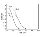
- FIG. 5 is a diagram showing an example of the extinction coefficient of the metal oxide film 25 according to the first embodiment.
- the horizontal axis indicates the wavelength
- the vertical axis indicates the extinction coefficient k.
- Extinction coefficients are measured, for example, by a spectroscopic ellipsometer. Extinction coefficients at wavelengths of 250 nm and below can be measured in a nitrogen purged environment, taking atmospheric absorption into account.
- the solid line indicates the extinction coefficient of the tantalum oxide film (Ta 2 O 5 film).
- the tantalum oxide film has an extinction coefficient with a maximum value of 0.1 or more in the wavelength range from 200 nm to 380 nm.
- the dotted line indicates the extinction coefficient of the niobium oxide film (Nb 2 O 5 film), and the broken line indicates the extinction coefficient of the tungsten oxide film (WO 3 film).
- the niobium oxide film and the tungsten oxide film each have a maximum extinction coefficient of 0.1 or more in the wavelength range from 200 nm to 380 nm. It can be seen that such a metal oxide film 25 absorbs a certain amount of light in the ultraviolet region.
- UV irradiation damage can be reduced compared to the case where the imaging device 1 does not have the metal oxide film 25. It is possible to suppress an increase in the interface level caused by the irradiation of ultraviolet light, and to suppress an increase in dark current. In addition, it is possible to suppress a decrease in the sensitivity of the pixels P to incident ultraviolet light, and suppress a decrease in the quantum efficiency of the pixels P.
- the metal oxide film 25 having a minimum extinction coefficient of 0.4 or more in the wavelength range of 200 nm to 250 nm and an average extinction coefficient of 0.09 or more in the wavelength range of 250 nm to 380 nm is provided.
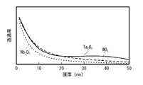
- FIG. 6 is a diagram showing an example of the relationship between the thickness of the metal oxide film 25 and the transmittance according to the first embodiment.
- the horizontal axis indicates the film thickness
- the vertical axis schematically indicates the transmittance to ultraviolet light.
- the solid line indicates the transmittance of the tantalum oxide film (Ta 2 O 5 film).
- a dotted line indicates the transmittance of the niobium oxide film (Nb 2 O 5 film), and a broken line indicates the transmittance of the tungsten oxide film (WO 3 film).
- the thickness of the metal oxide film 25 is greater than 20 nm, the transmittance is low, the amount of transmitted light is reduced, and the quantum efficiency is greatly reduced.
- the metal oxide film 25 is formed to have a film thickness of 1 nm or more and 20 nm or less. This makes it possible to suppress a decrease in the amount of light received by the photoelectric conversion unit 12 and ensure the quantum efficiency necessary for the imaging device 1 .
- the thickness of the metal oxide film 25 may be 1 nm or more and 10 nm or less. This makes it possible to effectively suppress a decrease in quantum efficiency.
- FIG. 7 to 11 are diagrams showing an example of the manufacturing method of the imaging device according to the first embodiment.
- a photodiode PD corresponding to each pixel P separated by an isolation portion 15 of a p-type semiconductor region is formed in a region of a silicon semiconductor substrate 10 where a pixel region is to be formed.
- the photodiode PD is formed over the entire thickness of the semiconductor substrate 10, and is configured as a pn junction photodiode composed of an n-type semiconductor region and a p-type semiconductor region facing both the front and back surfaces of the semiconductor substrate 10. .
- a p-type semiconductor well region is formed in contact with the isolation portion 15, and each pixel P is formed in this p-type semiconductor well region.
- a pixel transistor is formed.
- Each pixel transistor is formed to include a source region, a drain region, a gate insulating film, and a gate electrode.
- a multilayer wiring layer 90 is formed on the upper surface of the semiconductor substrate 10 opposite to the light incident surface, in which a plurality of wiring layers are arranged with an interlayer insulating film interposed therebetween.
- a chemical oxide film is formed on the rear surface of the substrate by chemical treatment.
- a fixed charge film 26 is formed on the light incident surface side of the semiconductor substrate 10 .
- an ALD (Atomic Layer Deposition) method is used to deposit, for example, aluminum oxide (Al 2 O 3 film) at a film-forming temperature of 200-300° C. so as to have a film thickness of 1-20 nm.
- the fixed charge film 26 is formed.
- a metal oxide film 25 is formed on the fixed charge film 26 .
- the metal oxide film 25 for example, tantalum oxide (Ta 2 O 5 ) may be deposited by reactive sputtering using a mixed gas of oxygen gas and argon gas. In this case, tantalum oxide is deposited at a deposition temperature of room temperature to 400° C. so as not to damage the wiring layer.
- the film thickness of tantalum oxide is set to about 1 nm to 20 nm. More desirably, the thickness of the tantalum oxide is about 1 nm to 10 nm.
- an oxide film is formed as an insulating film 24 on the metal oxide film 25 .
- the insulating film 24 is deposited at a deposition temperature of 400° C. or less by plasma CVD (Chemical Vapor Deposition), for example, so as not to damage the wiring layer.
- silicon oxide (SiO 2 ) is formed as the insulating film 24 with a film thickness of about 50 nm to 200 nm so as not to generate blisters.
- a light shielding portion 31 may be formed on the insulating film 24 .
- the light shielding portion 31 is formed by forming, for example, a metal film, more specifically tungsten (W), on the upper surface of the insulating film 24 by, for example, sputtering.
- the light blocking portion 31 may have a film thickness of 100 to 400 nm so as to block ultraviolet rays or stray light components other than ultraviolet rays. If the adhesion is poor, for example, titanium or the like may be deposited to a thickness of about 1 to 50 nm as the member 32, which is a barrier metal. Note that the light shielding portion 31 may not be provided if crosstalk in the effective pixel area for sensing light is not a concern. However, it is desirable that the pixels in the black reference pixel region are provided with the light shielding portion 31 .
- the light shielding portion 31 may be selectively etched away through a resist mask (not shown) to form the light shielding portion 31 at each pixel boundary. Wet etching or dry etching can be used for the etching, and the dry etching can obtain the fine line width of the light shielding portion 31 with high accuracy.
- the lens portion 21 is formed on the light incident surface side of the semiconductor substrate 10 .
- silicon oxide more specifically, silicon oxide by a plasma-enhanced chemical vapor deposition (PECVD) method using a gas containing tetraethoxysilane (TEOS) gas. is deposited at a deposition temperature of 400° C. or less.
- PECVD plasma-enhanced chemical vapor deposition
- TEOS tetraethoxysilane
- a silicon oxide film formed by the PECVD method using a gas containing this TEOS gas is called a P-TEOS film.
- the imaging device 1 shown in FIG. 3 can be manufactured by the manufacturing method as described above. It should be noted that the method of manufacturing the imaging device described above is merely an example, and other manufacturing methods may be used.
- a light receiving element (imaging device) 1 includes a metal oxide film 25 having a maximum extinction coefficient of 0.1 or more in a wavelength range from 200 nm to 380 nm, and ultraviolet light transmitted through the metal oxide film 25. and a light receiving portion (photoelectric conversion portion 12) that receives the light.
- the imaging device 1 Since the imaging device 1 according to the present embodiment has the metal oxide film 25 having a maximum extinction coefficient of 0.1 or more in the wavelength range from 200 nm to 380 nm, it ensures UV sensitivity and prevents UV irradiation damage. can be suppressed. It is possible to realize the imaging device 1 having high performance with respect to ultraviolet light.
- FIG. 12 is a block diagram showing an example of the overall configuration of an imaging device, which is an example of a light receiving element according to the second embodiment of the present disclosure.
- the imaging device 1 is, for example, a CMOS image sensor.
- the imaging device 1 includes a pixel section 100, a vertical drive circuit 111, a column readout circuit 112, a column signal processing circuit 113, a horizontal drive circuit 114, an output circuit 115, and a control circuit 116.
- the pixel portion 100, the vertical drive circuit 111, the column readout circuit 112, the column signal processing circuit 113, the horizontal drive circuit 114, the output circuit 115 and the control circuit 116 are formed on the same semiconductor substrate or on a plurality of layers electrically connected. It is provided on a semiconductor substrate.
- a plurality of pixels P are two-dimensionally arranged in a matrix.
- dummy pixels having no photodiode structure, light-shielding pixels whose light-receiving surface is shielded from outside light, and the like are arranged in rows and/or columns. May contain regions.
- pixel drive lines LD are formed along the left-right direction in the drawing (the direction in which pixels are arranged in pixel rows) for each row with respect to the matrix-like pixel arrangement, and vertical pixel wirings (
- a vertical signal line LV is formed along the vertical direction in the drawing (the direction in which pixels are arranged in a pixel column).
- One end of the pixel drive line LD is connected to an output terminal corresponding to each row of the vertical drive circuit 111 .
- the column readout circuit 112 includes at least a circuit that supplies a constant current for each column to the pixels P in the selected row in the pixel section 100, a current mirror circuit, a changeover switch for the pixels P to be read out, and the like.
- the column readout circuit 112 constitutes an amplifier together with the transistor in the selected pixel in the pixel section 100, converts the photocharge signal into a voltage signal, and outputs the voltage signal to the vertical signal line LV.
- the vertical driving circuit 111 includes a shift register, an address decoder, etc., and drives each pixel P of the pixel section 100 simultaneously or in units of rows.
- the vertical drive circuit 111 has a readout scanning system and a sweeping scanning system or a batch sweeping and batch transfer system, although the specific configuration thereof is omitted from the drawing.
- the readout scanning system In order to read out pixel signals from the pixels P, the readout scanning system sequentially selectively scans the pixels P of the pixel section 100 in units of rows. In the case of row driving (rolling shutter operation), sweep scanning is performed ahead of the readout scanning by the time of the shutter speed for the readout rows to be readout scanned by the readout scanning system.
- the signal read out by the readout operation by the readout scanning system corresponds to the amount of incident light after the immediately preceding readout operation or the electronic shutter operation.
- the period from the readout timing of the previous readout operation or the discharge timing of the electronic shutter operation to the readout timing of the current readout operation is the accumulation time (exposure time) of the photocharges in the pixels P.
- the time from batch sweeping to batch transfer is accumulation time (exposure time).
- a pixel signal output from each pixel P in a pixel row selectively scanned by the vertical drive circuit 111 is supplied to the column signal processing circuit 113 through each vertical signal line LV.
- the column signal processing circuit 113 performs predetermined signal processing on pixel signals output from the pixels P of the selected row through the vertical signal lines LV for each pixel column of the pixel section 100, and processes the pixel signals after the signal processing. is temporarily held.
- the column signal processing circuit 113 performs at least noise removal processing, such as CDS (Correlated Double Sampling) processing, as signal processing.
- the CDS processing by the column signal processing circuit 113 removes pixel-specific fixed pattern noise such as reset noise and variations in the threshold value of the amplification transistor AMP.
- the column signal processing circuit 113 may be configured to have, for example, an AD conversion function other than the noise removal process, so as to output the pixel signal as a digital signal.
- the horizontal driving circuit 114 includes shift registers, address decoders, etc., and sequentially selects unit circuits corresponding to the pixel columns of the column signal processing circuit 113 . Pixel signals processed by the column signal processing circuit 113 are sequentially output to the output circuit 115 by selective scanning by the horizontal driving circuit 114 .
- the control circuit 116 includes a timing generator for generating various timing signals, and drives the vertical driving circuit 111, the column signal processing circuit 113, the horizontal driving circuit 114, etc. based on the various timing signals generated by the timing generator. control.
- the imaging device 1 further includes an output circuit 115 and a data storage unit (not shown).
- the output circuit 115 has at least an addition processing function, and performs various signal processing such as addition processing on pixel signals output from the column signal processing circuit 113 .
- the data storage unit temporarily stores data required for signal processing in the output circuit 115 .
- the output circuit 115 and the data storage unit may be processed by an external signal processing unit such as a DSP (Digital Signal Processor) or software provided on a board different from that of the imaging device 1, or may be processed on the same board as the imaging device. may be mounted on top.
- DSP Digital Signal Processor
- FIG. 13 is a diagram illustrating a configuration example of pixels of an imaging device according to the second embodiment.
- Pixel P includes a photodiode PD.
- the photodiode PD is an example of a light receiving section (photoelectric conversion section 12).
- the photodiode PD is formed, for example, by forming a p-type layer on the substrate surface side of a p-type well layer formed on an n-type substrate and embedding an n-type buried layer. That is, such photodiodes are embedded photodiodes.
- the n-type buried layer has an impurity concentration such that it becomes depleted when the charges are discharged.
- the pixel P includes a TRY gate 41, a TX1 gate 42, a TX2 gate 43, and a charge holding portion (MEM) 44 in addition to the photodiode PD.
- the TRY gate 41 is a transfer section and is connected between the photodiode PD and the charge holding section 44 .
- the TX1 gate 42 and the TX2 gate 43 are transfer units, respectively, and are arranged near the charge holding unit 44 .
- the charge holding portion 44 is formed, for example, by forming a p-type layer on the substrate surface side of a p-type well layer formed on an n-type substrate and embedding an n-type buried layer.
- the n-type buried layer of the charge holding portion 44 may be formed of an n-type diffusion region.
- an n-type diffusion region may be formed inside the p-type well layer, and a p-type layer may be formed on the substrate surface side.
- the TRY gate 41 When the drive signal TRY is applied to the gate electrode of the TRY gate 41 , the charge is photoelectrically converted by the photodiode PD and accumulated inside the photodiode PD to be transferred to the charge holding unit 44 .
- the TRY gate 41 also functions as a gate for preventing the charge from flowing back from the charge holding portion 44 to the photodiode PD.
- the TX1 gate 42 functions as a gate when transferring charges from the charge holding portion 44 to a floating diffusion region (FD: Floating Diffusion), which will be described later.
- the TX1 gate 42 also functions as a gate for holding charges in the charge holding unit 44 .
- the TX2 gate 43 functions as a gate when transferring charges from the photodiode PD to the charge holding portion 44 .
- the TX2 gate 43 also functions as a gate for holding charges in the charge holding unit 44 .
- the drive signal TX2 and the drive signal TX1 are applied to the gate electrode of the TX2 gate 43 and the gate electrode of the TX1 gate 42, respectively, so that the charge holding section 44 is modulated. That is, by applying the drive signal TX2 and the drive signal TX1 to the gate electrode of the TX2 gate 43 and the gate electrode of the TX1 gate 42, respectively, the potential of the charge holding portion 44 can be deepened. As a result, the saturation charge amount of the charge holding unit 44 can be increased more than when no modulation is applied.
- the pixel P further includes a TRG gate 45 and a floating diffusion region 46.
- the TRG gate 45 is a transfer section, and transfers the charge accumulated in the charge holding section 44 to the floating diffusion region 46 by applying the drive signal TRG to the gate electrode.
- the floating diffusion region 46 is a charge-voltage conversion section including an n-type layer, and converts the charge transferred from the charge holding section 44 into a voltage by the TRG gate.
- the pixel P further includes a reset transistor (RST) 47, an amplification transistor (AMP) 48, and a selection transistor (SEL) 49.
- RST reset transistor
- AMP amplification transistor
- SEL selection transistor
- FIG. 13 shows an example in which n-channel MOS transistors are used for the reset transistor 47, the amplification transistor 48, and the selection transistor 49.
- the configurations of the reset transistor 47, amplification transistor 48 and selection transistor 49 are not limited to the example shown in FIG.
- the reset transistor 47 is connected between the power supply Vrst and the floating diffusion region 46 .
- the reset transistor 47 resets the floating diffusion region 46 by applying the drive signal RST to its gate electrode.
- the amplification transistor 48 has a drain electrode connected to the power supply Vdd and a gate electrode connected to the floating diffusion region 46, and the voltage of the floating diffusion region 46 is read out.
- the selection transistor 49 has a drain electrode connected to the source electrode of the amplification transistor 48 and a source electrode connected to the vertical signal line LV. The selection transistor 49 selects the pixel P from which the pixel signal is to be read by applying the driving signal SEL to the gate electrode.
- the selection transistor 49 is connected between the source electrode of the amplification transistor 48 and the vertical signal line LV. can be connected in between.
- One or more of the reset transistor 47, the amplification transistor 48 and the selection transistor 49 can be omitted depending on the pixel signal reading method.
- the pixel P is provided with an overflow gate (OFG) 50 for preventing blooming.
- the overflow gate 50 discharges the charge of the photodiode PD to the n-type layer 51 connected to the power supply Vdd by applying the drive signal OFG to the gate electrode at the start of exposure.
- the imaging device 1 having the pixels P described so far can realize a global shutter operation (global exposure) by simultaneously starting exposure of all pixels and ending exposure of all pixels simultaneously.
- This global shutter operation makes it possible to realize distortion-free imaging due to the exposure period that matches all pixels.
- the pixel P is formed by forming an n-type buried channel in the p-type well layer, but the opposite conductivity type may be used. In this case, all potential relationships are reversed.
- FIG. 14 is a diagram showing an example of a cross-sectional configuration of an imaging device according to the second embodiment.
- a charge holding portion (MEM) 44 is provided for each pixel P in the semiconductor substrate 10 .
- the light shielding portion 31 has an opening formed only in a region corresponding to the photoelectric conversion portion (photodiode) 12 so as to prevent light from entering a region other than the photoelectric conversion portion (photodiode) 12 . transmit light incident on the
- the charge holding portion 44 is located on the wiring layer side of the semiconductor substrate 10 and away from the irradiation surface side, so the light shielding portion 31 may not be provided. .
- the pixels in the black reference pixel region are provided with the light shielding portion 31 .
- Ultraviolet sensors are basically often used for Machine Vision inspections for industrial machinery. In machine vision inspection, it is strongly required to inspect samples flowing at high speed to reduce the time required, but with a rolling shutter, there is a risk of rolling shutter distortion and blurring of the moving object.
- the global shutter can simultaneously receive the light from the specimen at that moment in all pixels, so the above-mentioned problems do not occur and the inspection accuracy can be improved. That is, it is preferable to combine the imaging device 1 according to the present embodiment with a global shutter function. Also, as described above, it is possible to reduce the cost by eliminating the crosstalk suppression structure.
- the metal oxide film 25 may be composed of niobium oxide or tungsten oxide. Also, the metal oxide film 25 may be a multi-layer film containing two or more of tantalum oxide, niobium oxide, and tungsten oxide. Such a metal oxide film 25 is a material that absorbs a certain amount of ultraviolet light, and can suppress UV irradiation damage.
- the metal oxide film 25 is preferably made of a material whose standard free energy of formation (see "Metal Data Book 4th Edition, edited by The Japan Institute of Metals, Maruzen Publishing Co., Ltd.") is equal to or higher than the standard free energy of formation of silicon oxide. .
- the standard free energies of formation of tantalum oxide, niobium oxide, and tungsten oxide are each greater than the standard free energy of formation of silicon oxide.
- the metal oxide film 25 exhibits a larger "standard free energy of formation of oxide" than the silicon oxide forming the oxide film on the semiconductor substrate 10, the metal oxide film 25 is more likely to lose oxygen atoms than the oxide film. It is energetically more stable in terms of chemical reaction that oxygen atoms are deprived from . Therefore, the phenomenon that oxygen atoms are deprived from the oxide film by ultraviolet irradiation is suppressed, the interface layer between the oxide film and the surface of the semiconductor substrate 10 on the light incident surface side is protected, and dark current is generated due to the formation of the interface level. can be suppressed.
- tantalum oxide, niobium oxide, and tungsten oxide are preferable, and tantalum oxide is particularly preferable, as a result of evaluation of characteristics including defects of solid-state imaging devices.
- the imaging apparatus 1 and the like can be applied to any type of electronic equipment having an imaging function, such as a camera system such as a digital still camera or a video camera, or a mobile phone having an imaging function.
- FIG. 15 shows a schematic configuration of the electronic device 1000. As shown in FIG.
- the electronic device 1000 includes, for example, a lens group 1001, an imaging device 1, a DSP (Digital Signal Processor) circuit 1002, a frame memory 1003, a display unit 1004, a recording unit 1005, an operation unit 1006, and a power supply unit 1007. and are interconnected via a bus line 1008 .
- a lens group 1001 an imaging device 1
- a DSP (Digital Signal Processor) circuit 1002 a frame memory 1003, a display unit 1004, a recording unit 1005, an operation unit 1006, and a power supply unit 1007. and are interconnected via a bus line 1008 .
- DSP Digital Signal Processor
- a lens group 1001 captures incident light (image light) from a subject and forms an image on the imaging surface of the imaging device 1 .
- the imaging apparatus 1 converts the amount of incident light, which is imaged on the imaging surface by the lens group 1001 , into an electric signal for each pixel and supplies the electric signal to the DSP circuit 1002 as a pixel signal.
- the DSP circuit 1002 is a signal processing circuit that processes signals supplied from the imaging device 1 .
- a DSP circuit 1002 outputs image data obtained by processing a signal from the imaging device 1 .
- a frame memory 1003 temporarily holds image data processed by the DSP circuit 1002 in frame units.
- the display unit 1004 is, for example, a panel type display device such as a liquid crystal panel or an organic EL (Electro Luminescence) panel. to record.
- a panel type display device such as a liquid crystal panel or an organic EL (Electro Luminescence) panel. to record.
- the operation unit 1006 outputs operation signals for various functions of the electronic device 1000 in accordance with user's operations.
- the power supply unit 1007 appropriately supplies various power supplies to the DSP circuit 1002, the frame memory 1003, the display unit 1004, the recording unit 1005, and the operation unit 1006 as operating power supplies.
- the present disclosure has been described above with reference to the embodiments and modifications, the present technology is not limited to the above embodiments and the like, and various modifications are possible.
- the modified examples described above have been described as modified examples of the above-described embodiment, but the configurations of the modified examples can be appropriately combined.
- the present disclosure is not limited to back-illuminated image sensors, but is also applicable to front-illuminated image sensors.
- the present disclosure can also be configured as follows.
- the minimum value of the extinction coefficient of the metal oxide film in a wavelength range of 200 nm to 250 nm is 0.4 or more, The light receiving element according to (1), wherein the metal oxide film has an average extinction coefficient of 0.09 or more in a wavelength range from 250 nm to 380 nm.
- the wavelength range of the ultraviolet light includes a wavelength range from 200 nm to 380 nm
- the metal oxide film is made of at least one of tantalum oxide, niobium oxide, and tungsten oxide.
- the metal oxide film is made of tantalum oxide, The light receiving element according to any one of (1) to (5), wherein the thickness of the metal oxide film is 1 nm or more and 20 nm or less. (7) The light receiving element according to any one of (1) to (6), wherein the standard free energy of formation of the metal oxide film is greater than or equal to the standard free energy of formation of silicon oxide. (8) a lens that transmits ultraviolet light; a metal oxide film on which light transmitted through the lens is incident; a light-receiving unit that receives light transmitted through the lens and the metal oxide film, A light receiving element, wherein the metal oxide film has a maximum extinction coefficient of 0.1 or more in a wavelength range from 200 nm to 380 nm.
- the light receiving element according to (8), wherein the lens is made of silicon oxide.
- the minimum value of the extinction coefficient of the metal oxide film in a wavelength range of 200 nm to 250 nm is 0.4 or more,
- the light receiving element according to (8) or (9), wherein the average value of the extinction coefficient of the metal oxide film is 0.09 or more in a wavelength range from 250 nm to 380 nm.
- the light receiving element according to any one of (8) to (10), wherein the wavelength range of the ultraviolet light includes a wavelength range of 200 nm to 380 nm.
- the fixed charge film is made of aluminum oxide.
- a substrate provided with a plurality of the light-receiving portions that receive light and generate charges, holding portions that hold the charges, and transfer portions that transfer the charges generated in the light-receiving portions to the holding portion; a wiring layer provided on the side opposite to the side on which light is incident;
- a light-receiving element having a metal oxide film and a light-receiving portion that receives ultraviolet light transmitted through the metal oxide film, An electronic device, wherein the metal oxide film has a maximum extinction coefficient of 0.1 or more in a wavelength range from 200 nm to 380 nm.
- a light-receiving element having a lens that transmits ultraviolet light, a metal oxide film on which light transmitted through the lens is incident, and a light-receiving unit that receives the light transmitted through the lens and the metal oxide film, An electronic device, wherein the metal oxide film has a maximum extinction coefficient of 0.1 or more in a wavelength range from 200 nm to 380 nm.
Landscapes
- Physics & Mathematics (AREA)
- General Physics & Mathematics (AREA)
- Spectroscopy & Molecular Physics (AREA)
- Solid State Image Pick-Up Elements (AREA)
- Light Receiving Elements (AREA)
Priority Applications (3)
| Application Number | Priority Date | Filing Date | Title |
|---|---|---|---|
| US18/691,999 US20250133848A1 (en) | 2021-09-27 | 2022-03-24 | Light-receiving device and electronic apparatus |
| JP2023549354A JPWO2023047663A1 (https=) | 2021-09-27 | 2022-03-24 | |
| CN202280055065.9A CN117795689A (zh) | 2021-09-27 | 2022-03-24 | 光接收器件和电子设备 |
Applications Claiming Priority (2)
| Application Number | Priority Date | Filing Date | Title |
|---|---|---|---|
| JP2021157295 | 2021-09-27 | ||
| JP2021-157295 | 2021-09-27 |
Publications (1)
| Publication Number | Publication Date |
|---|---|
| WO2023047663A1 true WO2023047663A1 (ja) | 2023-03-30 |
Family
ID=85720388
Family Applications (1)
| Application Number | Title | Priority Date | Filing Date |
|---|---|---|---|
| PCT/JP2022/014049 Ceased WO2023047663A1 (ja) | 2021-09-27 | 2022-03-24 | 受光素子および電子機器 |
Country Status (5)
| Country | Link |
|---|---|
| US (1) | US20250133848A1 (https=) |
| JP (1) | JPWO2023047663A1 (https=) |
| CN (1) | CN117795689A (https=) |
| TW (1) | TW202315149A (https=) |
| WO (1) | WO2023047663A1 (https=) |
Citations (8)
| Publication number | Priority date | Publication date | Assignee | Title |
|---|---|---|---|---|
| JP2000068491A (ja) * | 1998-08-24 | 2000-03-03 | Nikon Corp | 撮像素子、撮像素子の製造方法および露光装置 |
| JP2001068658A (ja) * | 1999-08-27 | 2001-03-16 | Sony Corp | 固体撮像装置及びその製造方法 |
| WO2006028128A1 (ja) * | 2004-09-09 | 2006-03-16 | Matsushita Electric Industrial Co., Ltd. | 固体撮像素子 |
| JP2008306160A (ja) * | 2007-05-07 | 2008-12-18 | Sony Corp | 固体撮像装置とその製造方法および撮像装置 |
| US20120038015A1 (en) * | 2010-08-13 | 2012-02-16 | Taiwan Semiconductor Manufacturing Company, Ltd. | Antireflective layer for backside illuminated image sensor and method of manufacturing same |
| WO2019220897A1 (ja) * | 2018-05-18 | 2019-11-21 | ソニーセミコンダクタソリューションズ株式会社 | 撮像素子および電子機器並びに撮像素子の駆動方法 |
| WO2019230354A1 (ja) * | 2018-05-31 | 2019-12-05 | ソニー株式会社 | 光電変換素子および光電変換素子の製造方法 |
| JP2021132086A (ja) * | 2020-02-19 | 2021-09-09 | ソニーセミコンダクタソリューションズ株式会社 | 撮像装置及び電子機器 |
-
2022
- 2022-03-24 JP JP2023549354A patent/JPWO2023047663A1/ja active Pending
- 2022-03-24 WO PCT/JP2022/014049 patent/WO2023047663A1/ja not_active Ceased
- 2022-03-24 CN CN202280055065.9A patent/CN117795689A/zh active Pending
- 2022-03-24 US US18/691,999 patent/US20250133848A1/en active Pending
- 2022-04-08 TW TW111113363A patent/TW202315149A/zh unknown
Patent Citations (8)
| Publication number | Priority date | Publication date | Assignee | Title |
|---|---|---|---|---|
| JP2000068491A (ja) * | 1998-08-24 | 2000-03-03 | Nikon Corp | 撮像素子、撮像素子の製造方法および露光装置 |
| JP2001068658A (ja) * | 1999-08-27 | 2001-03-16 | Sony Corp | 固体撮像装置及びその製造方法 |
| WO2006028128A1 (ja) * | 2004-09-09 | 2006-03-16 | Matsushita Electric Industrial Co., Ltd. | 固体撮像素子 |
| JP2008306160A (ja) * | 2007-05-07 | 2008-12-18 | Sony Corp | 固体撮像装置とその製造方法および撮像装置 |
| US20120038015A1 (en) * | 2010-08-13 | 2012-02-16 | Taiwan Semiconductor Manufacturing Company, Ltd. | Antireflective layer for backside illuminated image sensor and method of manufacturing same |
| WO2019220897A1 (ja) * | 2018-05-18 | 2019-11-21 | ソニーセミコンダクタソリューションズ株式会社 | 撮像素子および電子機器並びに撮像素子の駆動方法 |
| WO2019230354A1 (ja) * | 2018-05-31 | 2019-12-05 | ソニー株式会社 | 光電変換素子および光電変換素子の製造方法 |
| JP2021132086A (ja) * | 2020-02-19 | 2021-09-09 | ソニーセミコンダクタソリューションズ株式会社 | 撮像装置及び電子機器 |
Also Published As
| Publication number | Publication date |
|---|---|
| US20250133848A1 (en) | 2025-04-24 |
| JPWO2023047663A1 (https=) | 2023-03-30 |
| CN117795689A (zh) | 2024-03-29 |
| TW202315149A (zh) | 2023-04-01 |
Similar Documents
| Publication | Publication Date | Title |
|---|---|---|
| US10306166B2 (en) | Solid-state imaging device, manufacturing method thereof, camera, and electronic device | |
| US10115762B2 (en) | Solid-state image pickup device, method of manufacturing thereof, and electronic apparatus | |
| KR102076422B1 (ko) | 고체 촬상 소자와 그 제조 방법, 고체 촬상 장치 및 촬상 장치 | |
| JP5564847B2 (ja) | 固体撮像装置とその製造方法、及び電子機器 | |
| US8183603B2 (en) | Solid-state imaging device for inhibiting dark current | |
| JP5663925B2 (ja) | 固体撮像装置、および、その製造方法、電子機器 | |
| US10854660B2 (en) | Solid-state image capturing element to suppress dark current, manufacturing method thereof, and electronic device | |
| TW201027727A (en) | Solid-state imaging device, method for manufacturing the same, and electronic apparatus | |
| JP2012104537A (ja) | 固体撮像装置とその製造方法、及び電子機器 | |
| US12080747B2 (en) | Solid-state imaging apparatus, method of manufacturing the same, and electronic device | |
| JP2013110285A (ja) | 固体撮像素子および製造方法、並びに、電子機器 | |
| WO2023047663A1 (ja) | 受光素子および電子機器 | |
| US10461119B2 (en) | Solid-state imaging device, imaging system, and method for manufacturing solid-state imaging device | |
| JP6663887B2 (ja) | 固体撮像装置、および、その製造方法、電子機器 |
Legal Events
| Date | Code | Title | Description |
|---|---|---|---|
| 121 | Ep: the epo has been informed by wipo that ep was designated in this application |
Ref document number: 22872422 Country of ref document: EP Kind code of ref document: A1 |
|
| WWE | Wipo information: entry into national phase |
Ref document number: 202280055065.9 Country of ref document: CN |
|
| WWE | Wipo information: entry into national phase |
Ref document number: 2023549354 Country of ref document: JP |
|
| WWE | Wipo information: entry into national phase |
Ref document number: 18691999 Country of ref document: US |
|
| NENP | Non-entry into the national phase |
Ref country code: DE |
|
| 122 | Ep: pct application non-entry in european phase |
Ref document number: 22872422 Country of ref document: EP Kind code of ref document: A1 |
|
| WWP | Wipo information: published in national office |
Ref document number: 18691999 Country of ref document: US |