WO2023047663A1 - Élément récepteur de lumière et dispositif électronique - Google Patents
Élément récepteur de lumière et dispositif électronique Download PDFInfo
- Publication number
- WO2023047663A1 WO2023047663A1 PCT/JP2022/014049 JP2022014049W WO2023047663A1 WO 2023047663 A1 WO2023047663 A1 WO 2023047663A1 JP 2022014049 W JP2022014049 W JP 2022014049W WO 2023047663 A1 WO2023047663 A1 WO 2023047663A1
- Authority
- WO
- WIPO (PCT)
- Prior art keywords
- light
- oxide film
- metal oxide
- receiving element
- element according
- Prior art date
Links
- 229910044991 metal oxide Inorganic materials 0.000 claims abstract description 104
- 150000004706 metal oxides Chemical class 0.000 claims abstract description 104
- 230000008033 biological extinction Effects 0.000 claims abstract description 38
- 239000000758 substrate Substances 0.000 claims description 51
- BPUBBGLMJRNUCC-UHFFFAOYSA-N oxygen(2-);tantalum(5+) Chemical compound [O-2].[O-2].[O-2].[O-2].[O-2].[Ta+5].[Ta+5] BPUBBGLMJRNUCC-UHFFFAOYSA-N 0.000 claims description 26
- 229910001936 tantalum oxide Inorganic materials 0.000 claims description 21
- VYPSYNLAJGMNEJ-UHFFFAOYSA-N Silicium dioxide Chemical compound O=[Si]=O VYPSYNLAJGMNEJ-UHFFFAOYSA-N 0.000 claims description 20
- 229910052814 silicon oxide Inorganic materials 0.000 claims description 20
- 238000012546 transfer Methods 0.000 claims description 16
- 230000015572 biosynthetic process Effects 0.000 claims description 15
- URLJKFSTXLNXLG-UHFFFAOYSA-N niobium(5+);oxygen(2-) Chemical compound [O-2].[O-2].[O-2].[O-2].[O-2].[Nb+5].[Nb+5] URLJKFSTXLNXLG-UHFFFAOYSA-N 0.000 claims description 12
- QGLKJKCYBOYXKC-UHFFFAOYSA-N nonaoxidotritungsten Chemical compound O=[W]1(=O)O[W](=O)(=O)O[W](=O)(=O)O1 QGLKJKCYBOYXKC-UHFFFAOYSA-N 0.000 claims description 12
- 229910001930 tungsten oxide Inorganic materials 0.000 claims description 12
- 229910000484 niobium oxide Inorganic materials 0.000 claims description 11
- 238000000034 method Methods 0.000 claims description 9
- TWNQGVIAIRXVLR-UHFFFAOYSA-N oxo(oxoalumanyloxy)alumane Chemical compound O=[Al]O[Al]=O TWNQGVIAIRXVLR-UHFFFAOYSA-N 0.000 claims description 5
- 238000003384 imaging method Methods 0.000 description 68
- 239000004065 semiconductor Substances 0.000 description 45
- 238000012545 processing Methods 0.000 description 40
- 239000010410 layer Substances 0.000 description 36
- 238000006243 chemical reaction Methods 0.000 description 31
- 238000010586 diagram Methods 0.000 description 15
- 238000009281 ultraviolet germicidal irradiation Methods 0.000 description 13
- 238000009792 diffusion process Methods 0.000 description 12
- 230000006870 function Effects 0.000 description 12
- 230000003321 amplification Effects 0.000 description 11
- 239000000463 material Substances 0.000 description 11
- 238000003199 nucleic acid amplification method Methods 0.000 description 11
- 230000000875 corresponding effect Effects 0.000 description 9
- 238000004519 manufacturing process Methods 0.000 description 9
- 238000012986 modification Methods 0.000 description 9
- 230000004048 modification Effects 0.000 description 9
- 230000035945 sensitivity Effects 0.000 description 8
- 238000002834 transmittance Methods 0.000 description 8
- 238000009825 accumulation Methods 0.000 description 6
- 239000007789 gas Substances 0.000 description 6
- 229910052751 metal Inorganic materials 0.000 description 6
- 238000002955 isolation Methods 0.000 description 5
- 239000002184 metal Substances 0.000 description 5
- 230000003287 optical effect Effects 0.000 description 5
- XUIMIQQOPSSXEZ-UHFFFAOYSA-N Silicon Chemical compound [Si] XUIMIQQOPSSXEZ-UHFFFAOYSA-N 0.000 description 4
- 238000002474 experimental method Methods 0.000 description 4
- 239000011159 matrix material Substances 0.000 description 4
- 229910052710 silicon Inorganic materials 0.000 description 4
- 239000010703 silicon Substances 0.000 description 4
- 238000010408 sweeping Methods 0.000 description 4
- 239000010936 titanium Substances 0.000 description 4
- 229910018072 Al 2 O 3 Inorganic materials 0.000 description 3
- BOTDANWDWHJENH-UHFFFAOYSA-N Tetraethyl orthosilicate Chemical compound CCO[Si](OCC)(OCC)OCC BOTDANWDWHJENH-UHFFFAOYSA-N 0.000 description 3
- RTAQQCXQSZGOHL-UHFFFAOYSA-N Titanium Chemical compound [Ti] RTAQQCXQSZGOHL-UHFFFAOYSA-N 0.000 description 3
- 229910052782 aluminium Inorganic materials 0.000 description 3
- XAGFODPZIPBFFR-UHFFFAOYSA-N aluminium Chemical compound [Al] XAGFODPZIPBFFR-UHFFFAOYSA-N 0.000 description 3
- 230000000903 blocking effect Effects 0.000 description 3
- 230000000052 comparative effect Effects 0.000 description 3
- 238000013500 data storage Methods 0.000 description 3
- 238000000151 deposition Methods 0.000 description 3
- 230000008021 deposition Effects 0.000 description 3
- 238000001312 dry etching Methods 0.000 description 3
- 230000000694 effects Effects 0.000 description 3
- 238000007689 inspection Methods 0.000 description 3
- 239000011229 interlayer Substances 0.000 description 3
- 125000004430 oxygen atom Chemical group O* 0.000 description 3
- 238000000623 plasma-assisted chemical vapour deposition Methods 0.000 description 3
- 230000008569 process Effects 0.000 description 3
- 238000005096 rolling process Methods 0.000 description 3
- 229910052719 titanium Inorganic materials 0.000 description 3
- WFKWXMTUELFFGS-UHFFFAOYSA-N tungsten Chemical compound [W] WFKWXMTUELFFGS-UHFFFAOYSA-N 0.000 description 3
- 229910052721 tungsten Inorganic materials 0.000 description 3
- 239000010937 tungsten Substances 0.000 description 3
- XKRFYHLGVUSROY-UHFFFAOYSA-N Argon Chemical compound [Ar] XKRFYHLGVUSROY-UHFFFAOYSA-N 0.000 description 2
- IJGRMHOSHXDMSA-UHFFFAOYSA-N Atomic nitrogen Chemical compound N#N IJGRMHOSHXDMSA-UHFFFAOYSA-N 0.000 description 2
- 229910052581 Si3N4 Inorganic materials 0.000 description 2
- 238000000231 atomic layer deposition Methods 0.000 description 2
- 230000004888 barrier function Effects 0.000 description 2
- 239000010949 copper Substances 0.000 description 2
- 230000005684 electric field Effects 0.000 description 2
- 238000005401 electroluminescence Methods 0.000 description 2
- 238000005530 etching Methods 0.000 description 2
- 239000011777 magnesium Substances 0.000 description 2
- 230000002093 peripheral effect Effects 0.000 description 2
- 229910021420 polycrystalline silicon Inorganic materials 0.000 description 2
- 229920005591 polysilicon Polymers 0.000 description 2
- 238000000926 separation method Methods 0.000 description 2
- LIVNPJMFVYWSIS-UHFFFAOYSA-N silicon monoxide Chemical compound [Si-]#[O+] LIVNPJMFVYWSIS-UHFFFAOYSA-N 0.000 description 2
- HQVNEWCFYHHQES-UHFFFAOYSA-N silicon nitride Chemical compound N12[Si]34N5[Si]62N3[Si]51N64 HQVNEWCFYHHQES-UHFFFAOYSA-N 0.000 description 2
- 239000000126 substance Substances 0.000 description 2
- RYGMFSIKBFXOCR-UHFFFAOYSA-N Copper Chemical compound [Cu] RYGMFSIKBFXOCR-UHFFFAOYSA-N 0.000 description 1
- MYMOFIZGZYHOMD-UHFFFAOYSA-N Dioxygen Chemical compound O=O MYMOFIZGZYHOMD-UHFFFAOYSA-N 0.000 description 1
- FYYHWMGAXLPEAU-UHFFFAOYSA-N Magnesium Chemical compound [Mg] FYYHWMGAXLPEAU-UHFFFAOYSA-N 0.000 description 1
- 229910008065 Si-SiO Inorganic materials 0.000 description 1
- 229910004298 SiO 2 Inorganic materials 0.000 description 1
- 229910006405 Si—SiO Inorganic materials 0.000 description 1
- 238000010521 absorption reaction Methods 0.000 description 1
- 230000009471 action Effects 0.000 description 1
- 229910052786 argon Inorganic materials 0.000 description 1
- 230000003139 buffering effect Effects 0.000 description 1
- 238000005229 chemical vapour deposition Methods 0.000 description 1
- 230000000295 complement effect Effects 0.000 description 1
- 239000000470 constituent Substances 0.000 description 1
- 229910052802 copper Inorganic materials 0.000 description 1
- 238000012937 correction Methods 0.000 description 1
- 230000002596 correlated effect Effects 0.000 description 1
- 230000003247 decreasing effect Effects 0.000 description 1
- 230000007547 defect Effects 0.000 description 1
- 238000013461 design Methods 0.000 description 1
- 230000006866 deterioration Effects 0.000 description 1
- 239000003989 dielectric material Substances 0.000 description 1
- 229910001882 dioxygen Inorganic materials 0.000 description 1
- 238000007599 discharging Methods 0.000 description 1
- 238000005516 engineering process Methods 0.000 description 1
- 238000011156 evaluation Methods 0.000 description 1
- 229910052735 hafnium Inorganic materials 0.000 description 1
- VBJZVLUMGGDVMO-UHFFFAOYSA-N hafnium atom Chemical compound [Hf] VBJZVLUMGGDVMO-UHFFFAOYSA-N 0.000 description 1
- 238000010438 heat treatment Methods 0.000 description 1
- 239000012535 impurity Substances 0.000 description 1
- 229910052747 lanthanoid Inorganic materials 0.000 description 1
- 150000002602 lanthanoids Chemical class 0.000 description 1
- 239000004973 liquid crystal related substance Substances 0.000 description 1
- 229910052749 magnesium Inorganic materials 0.000 description 1
- 239000007769 metal material Substances 0.000 description 1
- -1 more specifically Chemical compound 0.000 description 1
- 229910052757 nitrogen Inorganic materials 0.000 description 1
- 230000001151 other effect Effects 0.000 description 1
- 238000005268 plasma chemical vapour deposition Methods 0.000 description 1
- 230000005855 radiation Effects 0.000 description 1
- 238000005546 reactive sputtering Methods 0.000 description 1
- 230000009467 reduction Effects 0.000 description 1
- 238000005070 sampling Methods 0.000 description 1
- VSZWPYCFIRKVQL-UHFFFAOYSA-N selanylidenegallium;selenium Chemical compound [Se].[Se]=[Ga].[Se]=[Ga] VSZWPYCFIRKVQL-UHFFFAOYSA-N 0.000 description 1
- 239000002356 single layer Substances 0.000 description 1
- 238000004544 sputter deposition Methods 0.000 description 1
- 230000001629 suppression Effects 0.000 description 1
- 239000002344 surface layer Substances 0.000 description 1
- 229910052715 tantalum Inorganic materials 0.000 description 1
- GUVRBAGPIYLISA-UHFFFAOYSA-N tantalum atom Chemical compound [Ta] GUVRBAGPIYLISA-UHFFFAOYSA-N 0.000 description 1
- ZNOKGRXACCSDPY-UHFFFAOYSA-N tungsten trioxide Chemical compound O=[W](=O)=O ZNOKGRXACCSDPY-UHFFFAOYSA-N 0.000 description 1
- 238000001039 wet etching Methods 0.000 description 1
- 229910052727 yttrium Inorganic materials 0.000 description 1
- VWQVUPCCIRVNHF-UHFFFAOYSA-N yttrium atom Chemical compound [Y] VWQVUPCCIRVNHF-UHFFFAOYSA-N 0.000 description 1
Images


Classifications
-
- G—PHYSICS
- G01—MEASURING; TESTING
- G01J—MEASUREMENT OF INTENSITY, VELOCITY, SPECTRAL CONTENT, POLARISATION, PHASE OR PULSE CHARACTERISTICS OF INFRARED, VISIBLE OR ULTRAVIOLET LIGHT; COLORIMETRY; RADIATION PYROMETRY
- G01J1/00—Photometry, e.g. photographic exposure meter
- G01J1/02—Details
-
- H—ELECTRICITY
- H01—ELECTRIC ELEMENTS
- H01L—SEMICONDUCTOR DEVICES NOT COVERED BY CLASS H10
- H01L27/00—Devices consisting of a plurality of semiconductor or other solid-state components formed in or on a common substrate
- H01L27/14—Devices consisting of a plurality of semiconductor or other solid-state components formed in or on a common substrate including semiconductor components sensitive to infrared radiation, light, electromagnetic radiation of shorter wavelength or corpuscular radiation and specially adapted either for the conversion of the energy of such radiation into electrical energy or for the control of electrical energy by such radiation
- H01L27/144—Devices controlled by radiation
- H01L27/146—Imager structures
-
- H—ELECTRICITY
- H01—ELECTRIC ELEMENTS
- H01L—SEMICONDUCTOR DEVICES NOT COVERED BY CLASS H10
- H01L31/00—Semiconductor devices sensitive to infrared radiation, light, electromagnetic radiation of shorter wavelength or corpuscular radiation and specially adapted either for the conversion of the energy of such radiation into electrical energy or for the control of electrical energy by such radiation; Processes or apparatus specially adapted for the manufacture or treatment thereof or of parts thereof; Details thereof
- H01L31/08—Semiconductor devices sensitive to infrared radiation, light, electromagnetic radiation of shorter wavelength or corpuscular radiation and specially adapted either for the conversion of the energy of such radiation into electrical energy or for the control of electrical energy by such radiation; Processes or apparatus specially adapted for the manufacture or treatment thereof or of parts thereof; Details thereof in which radiation controls flow of current through the device, e.g. photoresistors
- H01L31/10—Semiconductor devices sensitive to infrared radiation, light, electromagnetic radiation of shorter wavelength or corpuscular radiation and specially adapted either for the conversion of the energy of such radiation into electrical energy or for the control of electrical energy by such radiation; Processes or apparatus specially adapted for the manufacture or treatment thereof or of parts thereof; Details thereof in which radiation controls flow of current through the device, e.g. photoresistors characterised by at least one potential-jump barrier or surface barrier, e.g. phototransistors
Landscapes
- Physics & Mathematics (AREA)
- Engineering & Computer Science (AREA)
- Power Engineering (AREA)
- General Physics & Mathematics (AREA)
- Electromagnetism (AREA)
- Condensed Matter Physics & Semiconductors (AREA)
- Computer Hardware Design (AREA)
- Microelectronics & Electronic Packaging (AREA)
- Spectroscopy & Molecular Physics (AREA)
- Solid State Image Pick-Up Elements (AREA)
- Light Receiving Elements (AREA)
Abstract
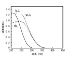
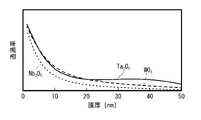
Un élément récepteur de lumière selon un mode de réalisation de la présente divulgation comprend : un film d'oxyde métallique (25) dont la valeur maximale d'un coefficient d'extinction dans une région de longueur d'onde de 200 nm à 380 nm est supérieure ou égale à 0,1 ; et une unité réceptrice de lumière (12) destinée à recevoir une lumière ultraviolette transmise à travers le film d'oxyde métallique (25).
Priority Applications (1)
| Application Number | Priority Date | Filing Date | Title |
|---|---|---|---|
| CN202280055065.9A CN117795689A (zh) | 2021-09-27 | 2022-03-24 | 光接收器件和电子设备 |
Applications Claiming Priority (2)
| Application Number | Priority Date | Filing Date | Title |
|---|---|---|---|
| JP2021157295 | 2021-09-27 | ||
| JP2021-157295 | 2021-09-27 |
Publications (1)
| Publication Number | Publication Date |
|---|---|
| WO2023047663A1 true WO2023047663A1 (fr) | 2023-03-30 |
Family
ID=85720388
Family Applications (1)
| Application Number | Title | Priority Date | Filing Date |
|---|---|---|---|
| PCT/JP2022/014049 WO2023047663A1 (fr) | 2021-09-27 | 2022-03-24 | Élément récepteur de lumière et dispositif électronique |
Country Status (3)
| Country | Link |
|---|---|
| CN (1) | CN117795689A (fr) |
| TW (1) | TW202315149A (fr) |
| WO (1) | WO2023047663A1 (fr) |
Citations (8)
| Publication number | Priority date | Publication date | Assignee | Title |
|---|---|---|---|---|
| JP2000068491A (ja) * | 1998-08-24 | 2000-03-03 | Nikon Corp | 撮像素子、撮像素子の製造方法および露光装置 |
| JP2001068658A (ja) * | 1999-08-27 | 2001-03-16 | Sony Corp | 固体撮像装置及びその製造方法 |
| WO2006028128A1 (fr) * | 2004-09-09 | 2006-03-16 | Matsushita Electric Industrial Co., Ltd. | Élément de détection d’image à semi-conducteur |
| JP2008306160A (ja) * | 2007-05-07 | 2008-12-18 | Sony Corp | 固体撮像装置とその製造方法および撮像装置 |
| US20120038015A1 (en) * | 2010-08-13 | 2012-02-16 | Taiwan Semiconductor Manufacturing Company, Ltd. | Antireflective layer for backside illuminated image sensor and method of manufacturing same |
| WO2019220897A1 (fr) * | 2018-05-18 | 2019-11-21 | ソニーセミコンダクタソリューションズ株式会社 | Élément d'imagerie, équipement électronique et procédé de commande d'élément d'imagerie |
| WO2019230354A1 (fr) * | 2018-05-31 | 2019-12-05 | ソニー株式会社 | Élément de conversion photoélectrique et procédé de fabrication d'élément de conversion photoélectrique |
| JP2021132086A (ja) * | 2020-02-19 | 2021-09-09 | ソニーセミコンダクタソリューションズ株式会社 | 撮像装置及び電子機器 |
-
2022
- 2022-03-24 WO PCT/JP2022/014049 patent/WO2023047663A1/fr active Application Filing
- 2022-03-24 CN CN202280055065.9A patent/CN117795689A/zh active Pending
- 2022-04-08 TW TW111113363A patent/TW202315149A/zh unknown
Patent Citations (8)
| Publication number | Priority date | Publication date | Assignee | Title |
|---|---|---|---|---|
| JP2000068491A (ja) * | 1998-08-24 | 2000-03-03 | Nikon Corp | 撮像素子、撮像素子の製造方法および露光装置 |
| JP2001068658A (ja) * | 1999-08-27 | 2001-03-16 | Sony Corp | 固体撮像装置及びその製造方法 |
| WO2006028128A1 (fr) * | 2004-09-09 | 2006-03-16 | Matsushita Electric Industrial Co., Ltd. | Élément de détection d’image à semi-conducteur |
| JP2008306160A (ja) * | 2007-05-07 | 2008-12-18 | Sony Corp | 固体撮像装置とその製造方法および撮像装置 |
| US20120038015A1 (en) * | 2010-08-13 | 2012-02-16 | Taiwan Semiconductor Manufacturing Company, Ltd. | Antireflective layer for backside illuminated image sensor and method of manufacturing same |
| WO2019220897A1 (fr) * | 2018-05-18 | 2019-11-21 | ソニーセミコンダクタソリューションズ株式会社 | Élément d'imagerie, équipement électronique et procédé de commande d'élément d'imagerie |
| WO2019230354A1 (fr) * | 2018-05-31 | 2019-12-05 | ソニー株式会社 | Élément de conversion photoélectrique et procédé de fabrication d'élément de conversion photoélectrique |
| JP2021132086A (ja) * | 2020-02-19 | 2021-09-09 | ソニーセミコンダクタソリューションズ株式会社 | 撮像装置及び電子機器 |
Also Published As
| Publication number | Publication date |
|---|---|
| TW202315149A (zh) | 2023-04-01 |
| CN117795689A (zh) | 2024-03-29 |
Similar Documents
| Publication | Publication Date | Title |
|---|---|---|
| US10306166B2 (en) | Solid-state imaging device, manufacturing method thereof, camera, and electronic device | |
| US10115762B2 (en) | Solid-state image pickup device, method of manufacturing thereof, and electronic apparatus | |
| KR102076422B1 (ko) | 고체 촬상 소자와 그 제조 방법, 고체 촬상 장치 및 촬상 장치 | |
| JP5564847B2 (ja) | 固体撮像装置とその製造方法、及び電子機器 | |
| CN106206635B (zh) | 摄像装置和电子设备 | |
| US8183603B2 (en) | Solid-state imaging device for inhibiting dark current | |
| JP5663925B2 (ja) | 固体撮像装置、および、その製造方法、電子機器 | |
| KR20100016308A (ko) | 고체 촬상 장치와 그 제조 방법 및 촬상 장치 | |
| TW201027727A (en) | Solid-state imaging device, method for manufacturing the same, and electronic apparatus | |
| US10854660B2 (en) | Solid-state image capturing element to suppress dark current, manufacturing method thereof, and electronic device | |
| JP2013110285A (ja) | 固体撮像素子および製造方法、並びに、電子機器 | |
| US20220005851A1 (en) | Solid-state imaging apparatus, method of manufacturing the same, and electronic device | |
| WO2023047663A1 (fr) | Élément récepteur de lumière et dispositif électronique | |
| US10461119B2 (en) | Solid-state imaging device, imaging system, and method for manufacturing solid-state imaging device | |
| JP6663887B2 (ja) | 固体撮像装置、および、その製造方法、電子機器 | |
| JPH08306895A (ja) | 固体撮像素子及び固体撮像素子の製造方法 | |
| JPH09129858A (ja) | 固体撮像素子及び固体撮像素子の製造方法 |
Legal Events
| Date | Code | Title | Description |
|---|---|---|---|
| 121 | Ep: the epo has been informed by wipo that ep was designated in this application |
Ref document number: 22872422 Country of ref document: EP Kind code of ref document: A1 |
|
| WWE | Wipo information: entry into national phase |
Ref document number: 2023549354 Country of ref document: JP |