WO2023047663A1 - Light-receiving element and electronic device - Google Patents
Light-receiving element and electronic device Download PDFInfo
- Publication number
- WO2023047663A1 WO2023047663A1 PCT/JP2022/014049 JP2022014049W WO2023047663A1 WO 2023047663 A1 WO2023047663 A1 WO 2023047663A1 JP 2022014049 W JP2022014049 W JP 2022014049W WO 2023047663 A1 WO2023047663 A1 WO 2023047663A1
- Authority
- WO
- WIPO (PCT)
- Prior art keywords
- light
- oxide film
- metal oxide
- receiving element
- element according
- Prior art date
Links
- 229910044991 metal oxide Inorganic materials 0.000 claims abstract description 104
- 150000004706 metal oxides Chemical class 0.000 claims abstract description 104
- 230000008033 biological extinction Effects 0.000 claims abstract description 38
- 239000000758 substrate Substances 0.000 claims description 51
- BPUBBGLMJRNUCC-UHFFFAOYSA-N oxygen(2-);tantalum(5+) Chemical compound [O-2].[O-2].[O-2].[O-2].[O-2].[Ta+5].[Ta+5] BPUBBGLMJRNUCC-UHFFFAOYSA-N 0.000 claims description 26
- 229910001936 tantalum oxide Inorganic materials 0.000 claims description 21
- VYPSYNLAJGMNEJ-UHFFFAOYSA-N Silicium dioxide Chemical compound O=[Si]=O VYPSYNLAJGMNEJ-UHFFFAOYSA-N 0.000 claims description 20
- 229910052814 silicon oxide Inorganic materials 0.000 claims description 20
- 238000012546 transfer Methods 0.000 claims description 16
- 230000015572 biosynthetic process Effects 0.000 claims description 15
- URLJKFSTXLNXLG-UHFFFAOYSA-N niobium(5+);oxygen(2-) Chemical compound [O-2].[O-2].[O-2].[O-2].[O-2].[Nb+5].[Nb+5] URLJKFSTXLNXLG-UHFFFAOYSA-N 0.000 claims description 12
- QGLKJKCYBOYXKC-UHFFFAOYSA-N nonaoxidotritungsten Chemical compound O=[W]1(=O)O[W](=O)(=O)O[W](=O)(=O)O1 QGLKJKCYBOYXKC-UHFFFAOYSA-N 0.000 claims description 12
- 229910001930 tungsten oxide Inorganic materials 0.000 claims description 12
- 229910000484 niobium oxide Inorganic materials 0.000 claims description 11
- 238000000034 method Methods 0.000 claims description 9
- TWNQGVIAIRXVLR-UHFFFAOYSA-N oxo(oxoalumanyloxy)alumane Chemical compound O=[Al]O[Al]=O TWNQGVIAIRXVLR-UHFFFAOYSA-N 0.000 claims description 5
- 238000003384 imaging method Methods 0.000 description 68
- 239000004065 semiconductor Substances 0.000 description 45
- 238000012545 processing Methods 0.000 description 40
- 239000010410 layer Substances 0.000 description 36
- 238000006243 chemical reaction Methods 0.000 description 31
- 238000010586 diagram Methods 0.000 description 15
- 238000009281 ultraviolet germicidal irradiation Methods 0.000 description 13
- 238000009792 diffusion process Methods 0.000 description 12
- 230000006870 function Effects 0.000 description 12
- 230000003321 amplification Effects 0.000 description 11
- 239000000463 material Substances 0.000 description 11
- 238000003199 nucleic acid amplification method Methods 0.000 description 11
- 230000000875 corresponding effect Effects 0.000 description 9
- 238000004519 manufacturing process Methods 0.000 description 9
- 238000012986 modification Methods 0.000 description 9
- 230000004048 modification Effects 0.000 description 9
- 230000035945 sensitivity Effects 0.000 description 8
- 238000002834 transmittance Methods 0.000 description 8
- 238000009825 accumulation Methods 0.000 description 6
- 239000007789 gas Substances 0.000 description 6
- 229910052751 metal Inorganic materials 0.000 description 6
- 238000002955 isolation Methods 0.000 description 5
- 239000002184 metal Substances 0.000 description 5
- 230000003287 optical effect Effects 0.000 description 5
- XUIMIQQOPSSXEZ-UHFFFAOYSA-N Silicon Chemical compound [Si] XUIMIQQOPSSXEZ-UHFFFAOYSA-N 0.000 description 4
- 238000002474 experimental method Methods 0.000 description 4
- 239000011159 matrix material Substances 0.000 description 4
- 229910052710 silicon Inorganic materials 0.000 description 4
- 239000010703 silicon Substances 0.000 description 4
- 238000010408 sweeping Methods 0.000 description 4
- 239000010936 titanium Substances 0.000 description 4
- 229910018072 Al 2 O 3 Inorganic materials 0.000 description 3
- BOTDANWDWHJENH-UHFFFAOYSA-N Tetraethyl orthosilicate Chemical compound CCO[Si](OCC)(OCC)OCC BOTDANWDWHJENH-UHFFFAOYSA-N 0.000 description 3
- RTAQQCXQSZGOHL-UHFFFAOYSA-N Titanium Chemical compound [Ti] RTAQQCXQSZGOHL-UHFFFAOYSA-N 0.000 description 3
- 229910052782 aluminium Inorganic materials 0.000 description 3
- XAGFODPZIPBFFR-UHFFFAOYSA-N aluminium Chemical compound [Al] XAGFODPZIPBFFR-UHFFFAOYSA-N 0.000 description 3
- 230000000903 blocking effect Effects 0.000 description 3
- 230000000052 comparative effect Effects 0.000 description 3
- 238000013500 data storage Methods 0.000 description 3
- 238000000151 deposition Methods 0.000 description 3
- 230000008021 deposition Effects 0.000 description 3
- 238000001312 dry etching Methods 0.000 description 3
- 230000000694 effects Effects 0.000 description 3
- 238000007689 inspection Methods 0.000 description 3
- 239000011229 interlayer Substances 0.000 description 3
- 125000004430 oxygen atom Chemical group O* 0.000 description 3
- 238000000623 plasma-assisted chemical vapour deposition Methods 0.000 description 3
- 230000008569 process Effects 0.000 description 3
- 238000005096 rolling process Methods 0.000 description 3
- 229910052719 titanium Inorganic materials 0.000 description 3
- WFKWXMTUELFFGS-UHFFFAOYSA-N tungsten Chemical compound [W] WFKWXMTUELFFGS-UHFFFAOYSA-N 0.000 description 3
- 229910052721 tungsten Inorganic materials 0.000 description 3
- 239000010937 tungsten Substances 0.000 description 3
- XKRFYHLGVUSROY-UHFFFAOYSA-N Argon Chemical compound [Ar] XKRFYHLGVUSROY-UHFFFAOYSA-N 0.000 description 2
- IJGRMHOSHXDMSA-UHFFFAOYSA-N Atomic nitrogen Chemical compound N#N IJGRMHOSHXDMSA-UHFFFAOYSA-N 0.000 description 2
- 229910052581 Si3N4 Inorganic materials 0.000 description 2
- 238000000231 atomic layer deposition Methods 0.000 description 2
- 230000004888 barrier function Effects 0.000 description 2
- 239000010949 copper Substances 0.000 description 2
- 230000005684 electric field Effects 0.000 description 2
- 238000005401 electroluminescence Methods 0.000 description 2
- 238000005530 etching Methods 0.000 description 2
- 239000011777 magnesium Substances 0.000 description 2
- 230000002093 peripheral effect Effects 0.000 description 2
- 229910021420 polycrystalline silicon Inorganic materials 0.000 description 2
- 229920005591 polysilicon Polymers 0.000 description 2
- 238000000926 separation method Methods 0.000 description 2
- LIVNPJMFVYWSIS-UHFFFAOYSA-N silicon monoxide Chemical compound [Si-]#[O+] LIVNPJMFVYWSIS-UHFFFAOYSA-N 0.000 description 2
- HQVNEWCFYHHQES-UHFFFAOYSA-N silicon nitride Chemical compound N12[Si]34N5[Si]62N3[Si]51N64 HQVNEWCFYHHQES-UHFFFAOYSA-N 0.000 description 2
- 239000000126 substance Substances 0.000 description 2
- RYGMFSIKBFXOCR-UHFFFAOYSA-N Copper Chemical compound [Cu] RYGMFSIKBFXOCR-UHFFFAOYSA-N 0.000 description 1
- MYMOFIZGZYHOMD-UHFFFAOYSA-N Dioxygen Chemical compound O=O MYMOFIZGZYHOMD-UHFFFAOYSA-N 0.000 description 1
- FYYHWMGAXLPEAU-UHFFFAOYSA-N Magnesium Chemical compound [Mg] FYYHWMGAXLPEAU-UHFFFAOYSA-N 0.000 description 1
- 229910008065 Si-SiO Inorganic materials 0.000 description 1
- 229910004298 SiO 2 Inorganic materials 0.000 description 1
- 229910006405 Si—SiO Inorganic materials 0.000 description 1
- 238000010521 absorption reaction Methods 0.000 description 1
- 230000009471 action Effects 0.000 description 1
- 229910052786 argon Inorganic materials 0.000 description 1
- 230000003139 buffering effect Effects 0.000 description 1
- 238000005229 chemical vapour deposition Methods 0.000 description 1
- 230000000295 complement effect Effects 0.000 description 1
- 239000000470 constituent Substances 0.000 description 1
- 229910052802 copper Inorganic materials 0.000 description 1
- 238000012937 correction Methods 0.000 description 1
- 230000002596 correlated effect Effects 0.000 description 1
- 230000003247 decreasing effect Effects 0.000 description 1
- 230000007547 defect Effects 0.000 description 1
- 238000013461 design Methods 0.000 description 1
- 230000006866 deterioration Effects 0.000 description 1
- 239000003989 dielectric material Substances 0.000 description 1
- 229910001882 dioxygen Inorganic materials 0.000 description 1
- 238000007599 discharging Methods 0.000 description 1
- 238000005516 engineering process Methods 0.000 description 1
- 238000011156 evaluation Methods 0.000 description 1
- 229910052735 hafnium Inorganic materials 0.000 description 1
- VBJZVLUMGGDVMO-UHFFFAOYSA-N hafnium atom Chemical compound [Hf] VBJZVLUMGGDVMO-UHFFFAOYSA-N 0.000 description 1
- 238000010438 heat treatment Methods 0.000 description 1
- 239000012535 impurity Substances 0.000 description 1
- 229910052747 lanthanoid Inorganic materials 0.000 description 1
- 150000002602 lanthanoids Chemical class 0.000 description 1
- 239000004973 liquid crystal related substance Substances 0.000 description 1
- 229910052749 magnesium Inorganic materials 0.000 description 1
- 239000007769 metal material Substances 0.000 description 1
- -1 more specifically Chemical compound 0.000 description 1
- 229910052757 nitrogen Inorganic materials 0.000 description 1
- 230000001151 other effect Effects 0.000 description 1
- 238000005268 plasma chemical vapour deposition Methods 0.000 description 1
- 230000005855 radiation Effects 0.000 description 1
- 238000005546 reactive sputtering Methods 0.000 description 1
- 230000009467 reduction Effects 0.000 description 1
- 238000005070 sampling Methods 0.000 description 1
- VSZWPYCFIRKVQL-UHFFFAOYSA-N selanylidenegallium;selenium Chemical compound [Se].[Se]=[Ga].[Se]=[Ga] VSZWPYCFIRKVQL-UHFFFAOYSA-N 0.000 description 1
- 239000002356 single layer Substances 0.000 description 1
- 238000004544 sputter deposition Methods 0.000 description 1
- 230000001629 suppression Effects 0.000 description 1
- 239000002344 surface layer Substances 0.000 description 1
- 229910052715 tantalum Inorganic materials 0.000 description 1
- GUVRBAGPIYLISA-UHFFFAOYSA-N tantalum atom Chemical compound [Ta] GUVRBAGPIYLISA-UHFFFAOYSA-N 0.000 description 1
- ZNOKGRXACCSDPY-UHFFFAOYSA-N tungsten trioxide Chemical compound O=[W](=O)=O ZNOKGRXACCSDPY-UHFFFAOYSA-N 0.000 description 1
- 238000001039 wet etching Methods 0.000 description 1
- 229910052727 yttrium Inorganic materials 0.000 description 1
- VWQVUPCCIRVNHF-UHFFFAOYSA-N yttrium atom Chemical compound [Y] VWQVUPCCIRVNHF-UHFFFAOYSA-N 0.000 description 1
Images


Classifications
-
- G—PHYSICS
- G01—MEASURING; TESTING
- G01J—MEASUREMENT OF INTENSITY, VELOCITY, SPECTRAL CONTENT, POLARISATION, PHASE OR PULSE CHARACTERISTICS OF INFRARED, VISIBLE OR ULTRAVIOLET LIGHT; COLORIMETRY; RADIATION PYROMETRY
- G01J1/00—Photometry, e.g. photographic exposure meter
- G01J1/02—Details
-
- H—ELECTRICITY
- H01—ELECTRIC ELEMENTS
- H01L—SEMICONDUCTOR DEVICES NOT COVERED BY CLASS H10
- H01L27/00—Devices consisting of a plurality of semiconductor or other solid-state components formed in or on a common substrate
- H01L27/14—Devices consisting of a plurality of semiconductor or other solid-state components formed in or on a common substrate including semiconductor components sensitive to infrared radiation, light, electromagnetic radiation of shorter wavelength or corpuscular radiation and specially adapted either for the conversion of the energy of such radiation into electrical energy or for the control of electrical energy by such radiation
- H01L27/144—Devices controlled by radiation
- H01L27/146—Imager structures
-
- H—ELECTRICITY
- H01—ELECTRIC ELEMENTS
- H01L—SEMICONDUCTOR DEVICES NOT COVERED BY CLASS H10
- H01L31/00—Semiconductor devices sensitive to infrared radiation, light, electromagnetic radiation of shorter wavelength or corpuscular radiation and specially adapted either for the conversion of the energy of such radiation into electrical energy or for the control of electrical energy by such radiation; Processes or apparatus specially adapted for the manufacture or treatment thereof or of parts thereof; Details thereof
- H01L31/08—Semiconductor devices sensitive to infrared radiation, light, electromagnetic radiation of shorter wavelength or corpuscular radiation and specially adapted either for the conversion of the energy of such radiation into electrical energy or for the control of electrical energy by such radiation; Processes or apparatus specially adapted for the manufacture or treatment thereof or of parts thereof; Details thereof in which radiation controls flow of current through the device, e.g. photoresistors
- H01L31/10—Semiconductor devices sensitive to infrared radiation, light, electromagnetic radiation of shorter wavelength or corpuscular radiation and specially adapted either for the conversion of the energy of such radiation into electrical energy or for the control of electrical energy by such radiation; Processes or apparatus specially adapted for the manufacture or treatment thereof or of parts thereof; Details thereof in which radiation controls flow of current through the device, e.g. photoresistors characterised by at least one potential-jump barrier or surface barrier, e.g. phototransistors
Definitions
- the present disclosure relates to light receiving elements and electronic devices.
- a photoelectric conversion element having an antireflection film composed of a silicon oxide film and a silicon nitride film having an extinction coefficient k of 0.01 or less in a wavelength range of 200 nm to 380 nm has been proposed (Patent Document 1). .
- a light receiving element of an embodiment of the present disclosure includes a metal oxide film having a maximum extinction coefficient of 0.1 or more in a wavelength range from 200 nm to 380 nm, and a light receiving portion that receives ultraviolet light transmitted through the metal oxide film.
- An electronic device includes a light receiving element having a metal oxide film and a light receiving unit that receives ultraviolet light transmitted through the metal oxide film.
- the maximum value of the extinction coefficient in the wavelength range from 200 nm to 380 nm of the metal oxide film is 0.1 or more.
- FIG. 1 is a block diagram showing an example of the overall configuration of an imaging device according to a first embodiment of the present disclosure
- FIG. It is a figure showing an example of a pixel part of an imaging device concerning a 1st embodiment of this indication. It is a figure showing an example of section composition of an imaging device concerning a 1st embodiment of this indication. It is a figure which shows an example of the result of an ultraviolet irradiation experiment.
- FIG. 3 is a diagram showing an example of an extinction coefficient of a metal oxide film according to the first embodiment of the present disclosure;
- FIG. 4 is a diagram showing an example of the relationship between the thickness of the metal oxide film and the transmittance according to the first embodiment of the present disclosure; It is a figure showing an example of a manufacturing method of an imaging device concerning a 1st embodiment of this indication. It is a figure showing an example of a manufacturing method of an imaging device concerning a 1st embodiment of this indication. It is a figure showing an example of a manufacturing method of an imaging device concerning a 1st embodiment of this indication. It is a figure showing an example of a manufacturing method of an imaging device concerning a 1st embodiment of this indication. It is a figure showing an example of a manufacturing method of an imaging device concerning a 1st embodiment of this indication. It is a figure showing an example of a manufacturing method of an imaging device concerning a 1st embodiment of this indication.
- FIG. 7 is a diagram illustrating a configuration example of pixels of an imaging device according to a second embodiment of the present disclosure; It is a figure showing an example of section composition of an imaging device concerning a 2nd embodiment of this indication.
- 1 is a block diagram showing a configuration example of an electronic device having an imaging device;
- FIG. 1 is a block diagram showing an example of the overall configuration of an imaging device, which is an example of a light receiving element according to the first embodiment of the present disclosure.
- the imaging device 1 which is a light receiving element, is an element that receives ultraviolet light and has sensitivity to ultraviolet light.
- the imaging device (light receiving element) 1 can be applied as an ultraviolet sensor (UV sensor) that detects ultraviolet rays.
- the imaging device 1 is, for example, a CMOS (Complementary Metal Oxide Semiconductor) image sensor.
- the imaging device 1 can be used in electronic devices such as digital still cameras and video cameras.
- the imaging device 1 pixels P having light receiving units (photoelectric conversion units) are arranged in a matrix.
- the imaging device 1 has, as an imaging area, a pixel section 100 in which a plurality of pixels P are two-dimensionally arranged in a matrix.
- the incident direction of light from the subject is the Z-axis direction
- the horizontal direction perpendicular to the Z-axis direction is the X-axis direction
- the vertical direction perpendicular to the Z-axis and the X-axis is the Y-axis direction.
- the imaging device 1 captures incident light (image light) from a subject via an optical lens system (not shown).
- the imaging device 1 captures an image of a subject.
- the imaging device 1 converts the amount of incident light formed on an imaging surface into an electric signal for each pixel, and outputs the electric signal as a pixel signal.
- the imaging device 1 has, for example, a vertical driving circuit 111, a column signal processing circuit 113, a horizontal driving circuit 114, an output circuit 115, a control circuit 116, an input/output terminal 117, and the like in a peripheral region of the pixel portion 100.
- a plurality of pixels P are two-dimensionally arranged in a matrix.
- the pixel unit 100 has a plurality of pixel rows each composed of a plurality of pixels P arranged in the horizontal direction (horizontal direction of the paper surface) and a plurality of pixel columns composed of a plurality of pixels P arranged in the vertical direction (vertical direction of the paper surface).
- the pixel unit 100 includes an effective pixel area for reading out signals based on signal charges generated by photoelectric conversion of light received from an object, and a black reference pixel for outputting optical black as a reference for the black level. area.
- the black reference pixel area is provided, for example, on the periphery of the effective pixel area.
- a pixel drive line Lread (row selection line and reset control line) is wired for each pixel row, and a vertical signal line Lsig is wired for each pixel column.
- the pixel drive line Lread transmits drive signals for reading signals from pixels.
- One end of the pixel drive line Lread is connected to an output terminal corresponding to each pixel row of the vertical drive circuit 111 .
- the vertical drive circuit 111 is composed of a shift register, an address decoder, and the like.
- the vertical drive circuit 111 is a pixel drive section that drives each pixel P of the pixel section 100, for example, in units of rows.
- the column signal processing circuit 113 is composed of amplifiers, horizontal selection switches, and the like provided for each vertical signal line Lsig. A signal output from each pixel P in a pixel row selectively scanned by the vertical driving circuit 111 is supplied to the column signal processing circuit 113 through the vertical signal line Lsig.
- the horizontal drive circuit 114 is composed of a shift register, an address decoder, etc., and sequentially drives the horizontal selection switches of the column signal processing circuit 113 while scanning them. By the selective scanning by the horizontal drive circuit 114, the signal of each pixel transmitted through each of the vertical signal lines Lsig is sequentially output to the horizontal signal line 121, and out of the substrate (semiconductor substrate) 10 through the horizontal signal line 121. transmitted.
- the output circuit 115 performs signal processing on signals sequentially supplied from each of the column signal processing circuits 113 via the horizontal signal line 121 and outputs the processed signals.
- the output circuit 115 may perform only buffering, or may perform black level adjustment, column variation correction, various digital signal processing, and the like.
- the column signal processing circuit 113 may perform signal processing such as noise removal and signal amplification based on the signal from the black reference pixel region.
- a circuit portion consisting of the vertical driving circuit 111, the column signal processing circuit 113, the horizontal driving circuit 114, the horizontal signal line 121 and the output circuit 115 may be formed on the substrate 10, or may be arranged on the external control IC. It can be anything. Moreover, those circuit portions may be formed on another substrate connected by a cable or the like.
- the control circuit 116 receives a clock given from the outside of the substrate 10, data instructing an operation mode, etc., and outputs data such as internal information of the imaging device 1.
- the control circuit 116 has a timing generator that generates various timing signals, and controls peripherals such as the vertical driving circuit 111, the column signal processing circuit 113, and the horizontal driving circuit 114 based on the various timing signals generated by the timing generator. Drive and control the circuit.
- the control circuit 116 generates, for example, a clock signal, a control signal, and the like, which serve as references for the operation of the vertical driving circuit 111, the column signal processing circuit 113, the horizontal driving circuit 114, and the like based on the vertical synchronization signal, the horizontal synchronization signal, and the master clock. to generate Clock signals and control signals generated by the control circuit 116 are input to the vertical drive circuit 111, the column signal processing circuit 113, the horizontal drive circuit 114, and the like.
- the input/output terminal 117 exchanges signals with the outside.
- FIG. 3 is a diagram illustrating an example of a cross-sectional configuration of an imaging device according to the first embodiment;
- the imaging device 1 has, for example, a configuration in which a substrate 10, a light guide section 20, and a multilayer wiring layer 90 are stacked in the Z-axis direction.
- the substrate 10 is a semiconductor substrate 10 having a first surface 11S1 and a second surface 11S2 facing each other.
- a light guide section 20 is provided on the first surface 11S1 side of the semiconductor substrate 10, and a multilayer wiring layer 90 is provided on the second surface 11S2 side of the semiconductor substrate 10. As shown in FIG.
- the imaging device 1 is a so-called back-illuminated imaging device.
- the semiconductor substrate 10 is composed of, for example, a silicon substrate.
- a light receiving portion of the pixel P is, for example, a photoelectric conversion portion 12 composed of a photodiode (PD), and has a pn junction in a predetermined region of the semiconductor substrate 10 .
- the photoelectric conversion part 12 is formed over the entire thickness direction of the semiconductor substrate 10, and is a pn junction type of an n-type semiconductor region and a p-type semiconductor region facing both the front and back surfaces of the semiconductor substrate 10.
- It is configured as a photodiode.
- the p-type semiconductor regions facing both the front and back surfaces of the semiconductor substrate 10 also serve as hole charge accumulation regions for suppressing dark current.
- the substrate 10 does not necessarily have to be a silicon substrate, and may be made of other semiconductor materials.
- the photoelectric conversion unit 12 is configured to have sensitivity in the ultraviolet wavelength range including the wavelength range from 200 nm to 380 nm.
- the photoelectric conversion unit 12 can photoelectrically convert incident ultraviolet light to generate electric charges.
- a plurality of photoelectric conversion units 12 are provided along the first surface 11S1 and the second surface 11S2.
- the multilayer wiring layer 90 has, for example, a structure in which a plurality of wiring layers are stacked with interlayer insulating layers interposed therebetween.
- a circuit (a transfer transistor, a reset transistor, an amplification transistor, etc.) for reading pixel signals based on charges generated by the photoelectric conversion unit 12 is formed in the semiconductor substrate 10 and the multilayer wiring layer 90 .
- the semiconductor substrate 10 and the multilayer wiring layer 90 are formed with, for example, the above-described vertical driving circuit 111, column signal processing circuit 113, horizontal driving circuit 114, output circuit 115, control circuit 116, input/output terminals 117, and the like.
- the pixel P has, for example, a transfer transistor, a reset transistor, a selection transistor, an amplification transistor (amplifier transistor), etc. as pixel transistors. Note that the pixel P does not have to have a selection transistor.
- Each pixel composed of a photoelectric conversion unit 12 and a pixel transistor is isolated by an isolation unit 15 formed of a p-type semiconductor region.
- the separation unit 15 is provided at the boundary between adjacent pixels P to separate the pixels P from each other.
- the isolation portion 15 is provided between adjacent photoelectric conversion portions 12 and can be said to be an element isolation region. Note that in FIG. 3 , a plurality of pixel transistors are represented by one pixel transistor and schematically represented by a gate electrode 91 .
- a plurality of wiring layers of the multilayer wiring layer 90 are formed using, for example, aluminum (Al), copper (Cu), tungsten (W), or the like.
- the wiring layer may be formed using polysilicon (Poly-Si).
- the interlayer insulating layer is, for example, a single layer film made of one of silicon oxide (SiO x ), silicon nitride (SiN x ), silicon oxynitride (SiO x N y ), etc., or two of these. It is formed of a laminated film composed of the above.
- the light guide portion 20 has a lens portion 21 for condensing light, an insulating film 24, a metal oxide film 25, and a fixed charge film 26.
- the light guide section 20 is laminated on the semiconductor substrate 10 in the thickness direction orthogonal to the first surface 11S1 of the semiconductor substrate 10 .
- the lens part 21 is an optical member also called an on-chip lens, and is provided on the insulating film 24 .
- Light from a subject enters the lens unit 21 through an optical lens system such as an imaging lens.
- the lens portion 21 is made of a material that transmits ultraviolet light, and guides incident light toward the photoelectric conversion portion 12 .
- the height of the lens portion 21 in the Z-axis direction that is, the thickness of the lens portion 21 in the Z-axis direction is set so that the light incident on the lens portion 21 is condensed on the photoelectric conversion portion 12 .
- the lens portion 21 is made of silicon oxide.
- the lens portion 21 can transmit incident ultraviolet light and focus it on the photoelectric conversion portion 12 .
- the lens portion 21 may be made of P-TEOS. In this case, the throughput of film formation can be improved.
- the lens portion 21 may be configured using a material containing silicon oxide, or may be configured using another material.
- the insulating film 24 is an insulating layer provided between the lens portion 21 and the photoelectric conversion portion 12 .
- the insulating film 24 is composed of, for example, an oxide film such as silicon oxide.
- the insulating film 24 may be made of P-TEOS. Note that the insulating film 24 may be configured using a material containing silicon oxide, or may be configured using another material.
- the fixed charge film 26 is provided between the insulating film 24 and the photoelectric conversion section 12 .
- the fixed charge film 26 is provided, for example, on an oxide film (not shown) formed on the first surface 11S1 of the semiconductor substrate 10. As shown in FIG. Fixed charge film 26 is formed to cover first surface 11S1 of semiconductor substrate 10 .
- the fixed charge film 26 is provided on the first surface 11S1 of the semiconductor substrate 10 so as to cover the portion where the photoelectric conversion portion 12 is formed and the portion where the separation portion 15 is formed. .
- the fixed charge film 26 is formed along the first surface 11S1 of the semiconductor substrate 10 so as to have a predetermined thickness.
- the fixed charge film 26 is, for example, a film having negative fixed charges and is formed using a high dielectric material. Since the fixed charge film 26 is formed to have negative fixed charges, an electric field is applied to the interface with the photoelectric conversion section 12 by the negative fixed charges. A positive charge (hole) accumulation region is formed by this electric field, and generation of dark current at the interface of the semiconductor substrate 10 can be suppressed.
- the fixed charge film 26 is made of, for example, hafnium (Hf), zirconium (Zr), aluminum (Al), tantalum (Ta), titanium (Ti), magnesium (Mg), yttrium (Y), lanthanide (La) elements, and the like. It is formed to include at least one of oxides.
- the fixed charge film 26 is made of aluminum oxide (Al 2 O 3 ).
- An aluminum oxide (Al 2 O 3 ) film is suitable for an ultraviolet sensor because it causes strong pinning and has a low extinction coefficient in the ultraviolet region.
- a film having a positive fixed charge may be provided as the fixed charge film 26 .
- the imaging device 1 may have a light shielding section 31 on the insulating film 24 as in the example shown in FIG.
- the light blocking portion 31 is configured by a member that blocks light, and is provided at the boundary between adjacent pixels P. As shown in FIG.
- the light blocking portion 31 is made of, for example, a metal material that blocks light, specifically tungsten, aluminum, or the like.
- the light shielding section 31 is a light shielding film provided around the photoelectric conversion section 12, and suppresses light leakage to surrounding pixels.
- the light shielding portion 31 may be made of a material that shields light, but a material that has a strong light shielding property and can be processed with high accuracy by microfabrication such as etching is preferable.
- a member 32 may be provided between the light shielding portion 31 and the insulating film 24 to improve the adhesion between the light shielding portion 31 and the insulating film 24 .
- This member 32 may be made of, for example, a barrier metal such as titanium.
- the member 32 can also be said to be an adhesion layer.
- trenches may be formed for separating the pixels P, and the trenches may be filled with an oxide film or a metal film.
- the metal oxide film 25 is a metal oxide film such as tantalum oxide (Ta 2 O 5 ) and is provided on the fixed charge film 26 .
- the metal oxide film 25 is laminated on the fixed charge film 26 between the lens portion 21 and the photoelectric conversion portion 12, for example.
- Photoelectric conversion portion 12 receives light that has passed through lens portion 21 and metal oxide film 25 .
- the photoelectric conversion unit 12 receives incident ultraviolet light through the lens unit 21 and the metal oxide film 25, and generates charges according to the amount of received light.
- the metal oxide film 25 is formed on substantially the entire surface of the fixed charge film 26 .
- the metal oxide film 25 does not necessarily have to be provided on substantially the entire surface of the fixed charge film 26, and may be provided only above the portion where the photoelectric conversion section 12 is formed, for example.
- the metal oxide film 25 and the fixed charge film 26 may also serve as an antireflection film that reduces reflection.
- the metal oxide film 25 may be composed of a single film, or may be composed of a plurality of laminated films.
- the metal oxide film 25 is composed of, for example, a tantalum oxide (Ta 2 O 5 ) film, a niobium oxide (Nb 2 O 5 ) film, a tungsten oxide (WO 3 ) film, or a laminated film thereof.
- the metal oxide film 25 is formed so that the maximum value of the extinction coefficient in the wavelength range from 200 nm to 380 nm is 0.1 or more. This makes it possible to suppress deterioration of characteristics due to ultraviolet irradiation while ensuring the quantum efficiency (QE) for light in the wavelength region of ultraviolet light.
- QE quantum efficiency
- a comparative example is a case where the imaging device 1 in FIG. 3 does not have the metal oxide film 25 .
- the inventors have confirmed that the sensitivity to ultraviolet light (UV sensitivity) can be improved in the imaging device 1 that does not have the metal oxide film 25 .
- UV irradiation damage when an ultraviolet irradiation experiment was conducted over a long period of time, it was found that the comparative example had a large increase in dark current and a large decrease in UV sensitivity (hereinafter referred to as UV irradiation damage).
- the inventors also investigated the relationship between the extinction coefficient of the metal oxide film 25 and the magnitude of UV irradiation damage (increase in dark current and decrease in UV sensitivity). As a result, it was found that UV irradiation damage can be suppressed by providing the metal oxide film 25 having a maximum extinction coefficient of 0.1 or more in the wavelength range from 200 nm to 380 nm. The reason why the UV irradiation damage can be suppressed is that the metal oxide film 25 reduces the UV irradiation to the Si interface of the semiconductor substrate 10, thereby suppressing the generation of interface states.
- FIG. 4 is a diagram showing an example of the results of an ultraviolet irradiation experiment.
- the wavelength of the irradiated ultraviolet rays is 193 nm, and the radiation intensity is 1.0 mW/cm 2 .
- the irradiation time of ultraviolet rays is 1 hour, and the total amount of radiant energy is 3.6 J/cm 2 .
- FIG. 4 shows the quantum efficiency and the amount of UV irradiation damage when there is no tantalum oxide (Ta 2 O 5 ) film and when there is a tantalum oxide (Ta 2 O 5 ) film with a thickness of about 5 nm. there is
- the initial quantum efficiency Qe is high, but the amount of quantum efficiency reduction due to UV irradiation is as large as 55%. Also, the dark signal corresponding to the amount of dark current increases by 1500 times.
- the initial quantum efficiency Qe decreased, but the amount of decrease in quantum efficiency due to UV irradiation was suppressed to 15%. Also, the dark signal is suppressed with an 80-fold increase. As described above, when the metal oxide film 25 is provided, the initial quantum efficiency Qe is lowered, but the effect of suppressing UV irradiation damage is high.
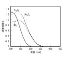
- FIG. 5 is a diagram showing an example of the extinction coefficient of the metal oxide film 25 according to the first embodiment.
- the horizontal axis indicates the wavelength
- the vertical axis indicates the extinction coefficient k.
- Extinction coefficients are measured, for example, by a spectroscopic ellipsometer. Extinction coefficients at wavelengths of 250 nm and below can be measured in a nitrogen purged environment, taking atmospheric absorption into account.
- the solid line indicates the extinction coefficient of the tantalum oxide film (Ta 2 O 5 film).
- the tantalum oxide film has an extinction coefficient with a maximum value of 0.1 or more in the wavelength range from 200 nm to 380 nm.
- the dotted line indicates the extinction coefficient of the niobium oxide film (Nb 2 O 5 film), and the broken line indicates the extinction coefficient of the tungsten oxide film (WO 3 film).
- the niobium oxide film and the tungsten oxide film each have a maximum extinction coefficient of 0.1 or more in the wavelength range from 200 nm to 380 nm. It can be seen that such a metal oxide film 25 absorbs a certain amount of light in the ultraviolet region.
- UV irradiation damage can be reduced compared to the case where the imaging device 1 does not have the metal oxide film 25. It is possible to suppress an increase in the interface level caused by the irradiation of ultraviolet light, and to suppress an increase in dark current. In addition, it is possible to suppress a decrease in the sensitivity of the pixels P to incident ultraviolet light, and suppress a decrease in the quantum efficiency of the pixels P.
- the metal oxide film 25 having a minimum extinction coefficient of 0.4 or more in the wavelength range of 200 nm to 250 nm and an average extinction coefficient of 0.09 or more in the wavelength range of 250 nm to 380 nm is provided.
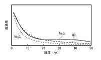
- FIG. 6 is a diagram showing an example of the relationship between the thickness of the metal oxide film 25 and the transmittance according to the first embodiment.
- the horizontal axis indicates the film thickness
- the vertical axis schematically indicates the transmittance to ultraviolet light.
- the solid line indicates the transmittance of the tantalum oxide film (Ta 2 O 5 film).
- a dotted line indicates the transmittance of the niobium oxide film (Nb 2 O 5 film), and a broken line indicates the transmittance of the tungsten oxide film (WO 3 film).
- the thickness of the metal oxide film 25 is greater than 20 nm, the transmittance is low, the amount of transmitted light is reduced, and the quantum efficiency is greatly reduced.
- the metal oxide film 25 is formed to have a film thickness of 1 nm or more and 20 nm or less. This makes it possible to suppress a decrease in the amount of light received by the photoelectric conversion unit 12 and ensure the quantum efficiency necessary for the imaging device 1 .
- the thickness of the metal oxide film 25 may be 1 nm or more and 10 nm or less. This makes it possible to effectively suppress a decrease in quantum efficiency.
- FIG. 7 to 11 are diagrams showing an example of the manufacturing method of the imaging device according to the first embodiment.
- a photodiode PD corresponding to each pixel P separated by an isolation portion 15 of a p-type semiconductor region is formed in a region of a silicon semiconductor substrate 10 where a pixel region is to be formed.
- the photodiode PD is formed over the entire thickness of the semiconductor substrate 10, and is configured as a pn junction photodiode composed of an n-type semiconductor region and a p-type semiconductor region facing both the front and back surfaces of the semiconductor substrate 10. .
- a p-type semiconductor well region is formed in contact with the isolation portion 15, and each pixel P is formed in this p-type semiconductor well region.
- a pixel transistor is formed.
- Each pixel transistor is formed to include a source region, a drain region, a gate insulating film, and a gate electrode.
- a multilayer wiring layer 90 is formed on the upper surface of the semiconductor substrate 10 opposite to the light incident surface, in which a plurality of wiring layers are arranged with an interlayer insulating film interposed therebetween.
- a chemical oxide film is formed on the rear surface of the substrate by chemical treatment.
- a fixed charge film 26 is formed on the light incident surface side of the semiconductor substrate 10 .
- an ALD (Atomic Layer Deposition) method is used to deposit, for example, aluminum oxide (Al 2 O 3 film) at a film-forming temperature of 200-300° C. so as to have a film thickness of 1-20 nm.
- the fixed charge film 26 is formed.
- a metal oxide film 25 is formed on the fixed charge film 26 .
- the metal oxide film 25 for example, tantalum oxide (Ta 2 O 5 ) may be deposited by reactive sputtering using a mixed gas of oxygen gas and argon gas. In this case, tantalum oxide is deposited at a deposition temperature of room temperature to 400° C. so as not to damage the wiring layer.
- the film thickness of tantalum oxide is set to about 1 nm to 20 nm. More desirably, the thickness of the tantalum oxide is about 1 nm to 10 nm.
- an oxide film is formed as an insulating film 24 on the metal oxide film 25 .
- the insulating film 24 is deposited at a deposition temperature of 400° C. or less by plasma CVD (Chemical Vapor Deposition), for example, so as not to damage the wiring layer.
- silicon oxide (SiO 2 ) is formed as the insulating film 24 with a film thickness of about 50 nm to 200 nm so as not to generate blisters.
- a light shielding portion 31 may be formed on the insulating film 24 .
- the light shielding portion 31 is formed by forming, for example, a metal film, more specifically tungsten (W), on the upper surface of the insulating film 24 by, for example, sputtering.
- the light blocking portion 31 may have a film thickness of 100 to 400 nm so as to block ultraviolet rays or stray light components other than ultraviolet rays. If the adhesion is poor, for example, titanium or the like may be deposited to a thickness of about 1 to 50 nm as the member 32, which is a barrier metal. Note that the light shielding portion 31 may not be provided if crosstalk in the effective pixel area for sensing light is not a concern. However, it is desirable that the pixels in the black reference pixel region are provided with the light shielding portion 31 .
- the light shielding portion 31 may be selectively etched away through a resist mask (not shown) to form the light shielding portion 31 at each pixel boundary. Wet etching or dry etching can be used for the etching, and the dry etching can obtain the fine line width of the light shielding portion 31 with high accuracy.
- the lens portion 21 is formed on the light incident surface side of the semiconductor substrate 10 .
- silicon oxide more specifically, silicon oxide by a plasma-enhanced chemical vapor deposition (PECVD) method using a gas containing tetraethoxysilane (TEOS) gas. is deposited at a deposition temperature of 400° C. or less.
- PECVD plasma-enhanced chemical vapor deposition
- TEOS tetraethoxysilane
- a silicon oxide film formed by the PECVD method using a gas containing this TEOS gas is called a P-TEOS film.
- the imaging device 1 shown in FIG. 3 can be manufactured by the manufacturing method as described above. It should be noted that the method of manufacturing the imaging device described above is merely an example, and other manufacturing methods may be used.
- a light receiving element (imaging device) 1 includes a metal oxide film 25 having a maximum extinction coefficient of 0.1 or more in a wavelength range from 200 nm to 380 nm, and ultraviolet light transmitted through the metal oxide film 25. and a light receiving portion (photoelectric conversion portion 12) that receives the light.
- the imaging device 1 Since the imaging device 1 according to the present embodiment has the metal oxide film 25 having a maximum extinction coefficient of 0.1 or more in the wavelength range from 200 nm to 380 nm, it ensures UV sensitivity and prevents UV irradiation damage. can be suppressed. It is possible to realize the imaging device 1 having high performance with respect to ultraviolet light.
- FIG. 12 is a block diagram showing an example of the overall configuration of an imaging device, which is an example of a light receiving element according to the second embodiment of the present disclosure.
- the imaging device 1 is, for example, a CMOS image sensor.
- the imaging device 1 includes a pixel section 100, a vertical drive circuit 111, a column readout circuit 112, a column signal processing circuit 113, a horizontal drive circuit 114, an output circuit 115, and a control circuit 116.
- the pixel portion 100, the vertical drive circuit 111, the column readout circuit 112, the column signal processing circuit 113, the horizontal drive circuit 114, the output circuit 115 and the control circuit 116 are formed on the same semiconductor substrate or on a plurality of layers electrically connected. It is provided on a semiconductor substrate.
- a plurality of pixels P are two-dimensionally arranged in a matrix.
- dummy pixels having no photodiode structure, light-shielding pixels whose light-receiving surface is shielded from outside light, and the like are arranged in rows and/or columns. May contain regions.
- pixel drive lines LD are formed along the left-right direction in the drawing (the direction in which pixels are arranged in pixel rows) for each row with respect to the matrix-like pixel arrangement, and vertical pixel wirings (
- a vertical signal line LV is formed along the vertical direction in the drawing (the direction in which pixels are arranged in a pixel column).
- One end of the pixel drive line LD is connected to an output terminal corresponding to each row of the vertical drive circuit 111 .
- the column readout circuit 112 includes at least a circuit that supplies a constant current for each column to the pixels P in the selected row in the pixel section 100, a current mirror circuit, a changeover switch for the pixels P to be read out, and the like.
- the column readout circuit 112 constitutes an amplifier together with the transistor in the selected pixel in the pixel section 100, converts the photocharge signal into a voltage signal, and outputs the voltage signal to the vertical signal line LV.
- the vertical driving circuit 111 includes a shift register, an address decoder, etc., and drives each pixel P of the pixel section 100 simultaneously or in units of rows.
- the vertical drive circuit 111 has a readout scanning system and a sweeping scanning system or a batch sweeping and batch transfer system, although the specific configuration thereof is omitted from the drawing.
- the readout scanning system In order to read out pixel signals from the pixels P, the readout scanning system sequentially selectively scans the pixels P of the pixel section 100 in units of rows. In the case of row driving (rolling shutter operation), sweep scanning is performed ahead of the readout scanning by the time of the shutter speed for the readout rows to be readout scanned by the readout scanning system.
- the signal read out by the readout operation by the readout scanning system corresponds to the amount of incident light after the immediately preceding readout operation or the electronic shutter operation.
- the period from the readout timing of the previous readout operation or the discharge timing of the electronic shutter operation to the readout timing of the current readout operation is the accumulation time (exposure time) of the photocharges in the pixels P.
- the time from batch sweeping to batch transfer is accumulation time (exposure time).
- a pixel signal output from each pixel P in a pixel row selectively scanned by the vertical drive circuit 111 is supplied to the column signal processing circuit 113 through each vertical signal line LV.
- the column signal processing circuit 113 performs predetermined signal processing on pixel signals output from the pixels P of the selected row through the vertical signal lines LV for each pixel column of the pixel section 100, and processes the pixel signals after the signal processing. is temporarily held.
- the column signal processing circuit 113 performs at least noise removal processing, such as CDS (Correlated Double Sampling) processing, as signal processing.
- the CDS processing by the column signal processing circuit 113 removes pixel-specific fixed pattern noise such as reset noise and variations in the threshold value of the amplification transistor AMP.
- the column signal processing circuit 113 may be configured to have, for example, an AD conversion function other than the noise removal process, so as to output the pixel signal as a digital signal.
- the horizontal driving circuit 114 includes shift registers, address decoders, etc., and sequentially selects unit circuits corresponding to the pixel columns of the column signal processing circuit 113 . Pixel signals processed by the column signal processing circuit 113 are sequentially output to the output circuit 115 by selective scanning by the horizontal driving circuit 114 .
- the control circuit 116 includes a timing generator for generating various timing signals, and drives the vertical driving circuit 111, the column signal processing circuit 113, the horizontal driving circuit 114, etc. based on the various timing signals generated by the timing generator. control.
- the imaging device 1 further includes an output circuit 115 and a data storage unit (not shown).
- the output circuit 115 has at least an addition processing function, and performs various signal processing such as addition processing on pixel signals output from the column signal processing circuit 113 .
- the data storage unit temporarily stores data required for signal processing in the output circuit 115 .
- the output circuit 115 and the data storage unit may be processed by an external signal processing unit such as a DSP (Digital Signal Processor) or software provided on a board different from that of the imaging device 1, or may be processed on the same board as the imaging device. may be mounted on top.
- DSP Digital Signal Processor
- FIG. 13 is a diagram illustrating a configuration example of pixels of an imaging device according to the second embodiment.
- Pixel P includes a photodiode PD.
- the photodiode PD is an example of a light receiving section (photoelectric conversion section 12).
- the photodiode PD is formed, for example, by forming a p-type layer on the substrate surface side of a p-type well layer formed on an n-type substrate and embedding an n-type buried layer. That is, such photodiodes are embedded photodiodes.
- the n-type buried layer has an impurity concentration such that it becomes depleted when the charges are discharged.
- the pixel P includes a TRY gate 41, a TX1 gate 42, a TX2 gate 43, and a charge holding portion (MEM) 44 in addition to the photodiode PD.
- the TRY gate 41 is a transfer section and is connected between the photodiode PD and the charge holding section 44 .
- the TX1 gate 42 and the TX2 gate 43 are transfer units, respectively, and are arranged near the charge holding unit 44 .
- the charge holding portion 44 is formed, for example, by forming a p-type layer on the substrate surface side of a p-type well layer formed on an n-type substrate and embedding an n-type buried layer.
- the n-type buried layer of the charge holding portion 44 may be formed of an n-type diffusion region.
- an n-type diffusion region may be formed inside the p-type well layer, and a p-type layer may be formed on the substrate surface side.
- the TRY gate 41 When the drive signal TRY is applied to the gate electrode of the TRY gate 41 , the charge is photoelectrically converted by the photodiode PD and accumulated inside the photodiode PD to be transferred to the charge holding unit 44 .
- the TRY gate 41 also functions as a gate for preventing the charge from flowing back from the charge holding portion 44 to the photodiode PD.
- the TX1 gate 42 functions as a gate when transferring charges from the charge holding portion 44 to a floating diffusion region (FD: Floating Diffusion), which will be described later.
- the TX1 gate 42 also functions as a gate for holding charges in the charge holding unit 44 .
- the TX2 gate 43 functions as a gate when transferring charges from the photodiode PD to the charge holding portion 44 .
- the TX2 gate 43 also functions as a gate for holding charges in the charge holding unit 44 .
- the drive signal TX2 and the drive signal TX1 are applied to the gate electrode of the TX2 gate 43 and the gate electrode of the TX1 gate 42, respectively, so that the charge holding section 44 is modulated. That is, by applying the drive signal TX2 and the drive signal TX1 to the gate electrode of the TX2 gate 43 and the gate electrode of the TX1 gate 42, respectively, the potential of the charge holding portion 44 can be deepened. As a result, the saturation charge amount of the charge holding unit 44 can be increased more than when no modulation is applied.
- the pixel P further includes a TRG gate 45 and a floating diffusion region 46.
- the TRG gate 45 is a transfer section, and transfers the charge accumulated in the charge holding section 44 to the floating diffusion region 46 by applying the drive signal TRG to the gate electrode.
- the floating diffusion region 46 is a charge-voltage conversion section including an n-type layer, and converts the charge transferred from the charge holding section 44 into a voltage by the TRG gate.
- the pixel P further includes a reset transistor (RST) 47, an amplification transistor (AMP) 48, and a selection transistor (SEL) 49.
- RST reset transistor
- AMP amplification transistor
- SEL selection transistor
- FIG. 13 shows an example in which n-channel MOS transistors are used for the reset transistor 47, the amplification transistor 48, and the selection transistor 49.
- the configurations of the reset transistor 47, amplification transistor 48 and selection transistor 49 are not limited to the example shown in FIG.
- the reset transistor 47 is connected between the power supply Vrst and the floating diffusion region 46 .
- the reset transistor 47 resets the floating diffusion region 46 by applying the drive signal RST to its gate electrode.
- the amplification transistor 48 has a drain electrode connected to the power supply Vdd and a gate electrode connected to the floating diffusion region 46, and the voltage of the floating diffusion region 46 is read out.
- the selection transistor 49 has a drain electrode connected to the source electrode of the amplification transistor 48 and a source electrode connected to the vertical signal line LV. The selection transistor 49 selects the pixel P from which the pixel signal is to be read by applying the driving signal SEL to the gate electrode.
- the selection transistor 49 is connected between the source electrode of the amplification transistor 48 and the vertical signal line LV. can be connected in between.
- One or more of the reset transistor 47, the amplification transistor 48 and the selection transistor 49 can be omitted depending on the pixel signal reading method.
- the pixel P is provided with an overflow gate (OFG) 50 for preventing blooming.
- the overflow gate 50 discharges the charge of the photodiode PD to the n-type layer 51 connected to the power supply Vdd by applying the drive signal OFG to the gate electrode at the start of exposure.
- the imaging device 1 having the pixels P described so far can realize a global shutter operation (global exposure) by simultaneously starting exposure of all pixels and ending exposure of all pixels simultaneously.
- This global shutter operation makes it possible to realize distortion-free imaging due to the exposure period that matches all pixels.
- the pixel P is formed by forming an n-type buried channel in the p-type well layer, but the opposite conductivity type may be used. In this case, all potential relationships are reversed.
- FIG. 14 is a diagram showing an example of a cross-sectional configuration of an imaging device according to the second embodiment.
- a charge holding portion (MEM) 44 is provided for each pixel P in the semiconductor substrate 10 .
- the light shielding portion 31 has an opening formed only in a region corresponding to the photoelectric conversion portion (photodiode) 12 so as to prevent light from entering a region other than the photoelectric conversion portion (photodiode) 12 . transmit light incident on the
- the charge holding portion 44 is located on the wiring layer side of the semiconductor substrate 10 and away from the irradiation surface side, so the light shielding portion 31 may not be provided. .
- the pixels in the black reference pixel region are provided with the light shielding portion 31 .
- Ultraviolet sensors are basically often used for Machine Vision inspections for industrial machinery. In machine vision inspection, it is strongly required to inspect samples flowing at high speed to reduce the time required, but with a rolling shutter, there is a risk of rolling shutter distortion and blurring of the moving object.
- the global shutter can simultaneously receive the light from the specimen at that moment in all pixels, so the above-mentioned problems do not occur and the inspection accuracy can be improved. That is, it is preferable to combine the imaging device 1 according to the present embodiment with a global shutter function. Also, as described above, it is possible to reduce the cost by eliminating the crosstalk suppression structure.
- the metal oxide film 25 may be composed of niobium oxide or tungsten oxide. Also, the metal oxide film 25 may be a multi-layer film containing two or more of tantalum oxide, niobium oxide, and tungsten oxide. Such a metal oxide film 25 is a material that absorbs a certain amount of ultraviolet light, and can suppress UV irradiation damage.
- the metal oxide film 25 is preferably made of a material whose standard free energy of formation (see "Metal Data Book 4th Edition, edited by The Japan Institute of Metals, Maruzen Publishing Co., Ltd.") is equal to or higher than the standard free energy of formation of silicon oxide. .
- the standard free energies of formation of tantalum oxide, niobium oxide, and tungsten oxide are each greater than the standard free energy of formation of silicon oxide.
- the metal oxide film 25 exhibits a larger "standard free energy of formation of oxide" than the silicon oxide forming the oxide film on the semiconductor substrate 10, the metal oxide film 25 is more likely to lose oxygen atoms than the oxide film. It is energetically more stable in terms of chemical reaction that oxygen atoms are deprived from . Therefore, the phenomenon that oxygen atoms are deprived from the oxide film by ultraviolet irradiation is suppressed, the interface layer between the oxide film and the surface of the semiconductor substrate 10 on the light incident surface side is protected, and dark current is generated due to the formation of the interface level. can be suppressed.
- tantalum oxide, niobium oxide, and tungsten oxide are preferable, and tantalum oxide is particularly preferable, as a result of evaluation of characteristics including defects of solid-state imaging devices.
- the imaging apparatus 1 and the like can be applied to any type of electronic equipment having an imaging function, such as a camera system such as a digital still camera or a video camera, or a mobile phone having an imaging function.
- FIG. 15 shows a schematic configuration of the electronic device 1000. As shown in FIG.
- the electronic device 1000 includes, for example, a lens group 1001, an imaging device 1, a DSP (Digital Signal Processor) circuit 1002, a frame memory 1003, a display unit 1004, a recording unit 1005, an operation unit 1006, and a power supply unit 1007. and are interconnected via a bus line 1008 .
- a lens group 1001 an imaging device 1
- a DSP (Digital Signal Processor) circuit 1002 a frame memory 1003, a display unit 1004, a recording unit 1005, an operation unit 1006, and a power supply unit 1007. and are interconnected via a bus line 1008 .
- DSP Digital Signal Processor
- a lens group 1001 captures incident light (image light) from a subject and forms an image on the imaging surface of the imaging device 1 .
- the imaging apparatus 1 converts the amount of incident light, which is imaged on the imaging surface by the lens group 1001 , into an electric signal for each pixel and supplies the electric signal to the DSP circuit 1002 as a pixel signal.
- the DSP circuit 1002 is a signal processing circuit that processes signals supplied from the imaging device 1 .
- a DSP circuit 1002 outputs image data obtained by processing a signal from the imaging device 1 .
- a frame memory 1003 temporarily holds image data processed by the DSP circuit 1002 in frame units.
- the display unit 1004 is, for example, a panel type display device such as a liquid crystal panel or an organic EL (Electro Luminescence) panel. to record.
- a panel type display device such as a liquid crystal panel or an organic EL (Electro Luminescence) panel. to record.
- the operation unit 1006 outputs operation signals for various functions of the electronic device 1000 in accordance with user's operations.
- the power supply unit 1007 appropriately supplies various power supplies to the DSP circuit 1002, the frame memory 1003, the display unit 1004, the recording unit 1005, and the operation unit 1006 as operating power supplies.
- the present disclosure has been described above with reference to the embodiments and modifications, the present technology is not limited to the above embodiments and the like, and various modifications are possible.
- the modified examples described above have been described as modified examples of the above-described embodiment, but the configurations of the modified examples can be appropriately combined.
- the present disclosure is not limited to back-illuminated image sensors, but is also applicable to front-illuminated image sensors.
- the present disclosure can also be configured as follows.
- the minimum value of the extinction coefficient of the metal oxide film in a wavelength range of 200 nm to 250 nm is 0.4 or more, The light receiving element according to (1), wherein the metal oxide film has an average extinction coefficient of 0.09 or more in a wavelength range from 250 nm to 380 nm.
- the wavelength range of the ultraviolet light includes a wavelength range from 200 nm to 380 nm
- the metal oxide film is made of at least one of tantalum oxide, niobium oxide, and tungsten oxide.
- the metal oxide film is made of tantalum oxide, The light receiving element according to any one of (1) to (5), wherein the thickness of the metal oxide film is 1 nm or more and 20 nm or less. (7) The light receiving element according to any one of (1) to (6), wherein the standard free energy of formation of the metal oxide film is greater than or equal to the standard free energy of formation of silicon oxide. (8) a lens that transmits ultraviolet light; a metal oxide film on which light transmitted through the lens is incident; a light-receiving unit that receives light transmitted through the lens and the metal oxide film, A light receiving element, wherein the metal oxide film has a maximum extinction coefficient of 0.1 or more in a wavelength range from 200 nm to 380 nm.
- the light receiving element according to (8), wherein the lens is made of silicon oxide.
- the minimum value of the extinction coefficient of the metal oxide film in a wavelength range of 200 nm to 250 nm is 0.4 or more,
- the light receiving element according to (8) or (9), wherein the average value of the extinction coefficient of the metal oxide film is 0.09 or more in a wavelength range from 250 nm to 380 nm.
- the light receiving element according to any one of (8) to (10), wherein the wavelength range of the ultraviolet light includes a wavelength range of 200 nm to 380 nm.
- the fixed charge film is made of aluminum oxide.
- a substrate provided with a plurality of the light-receiving portions that receive light and generate charges, holding portions that hold the charges, and transfer portions that transfer the charges generated in the light-receiving portions to the holding portion; a wiring layer provided on the side opposite to the side on which light is incident;
- a light-receiving element having a metal oxide film and a light-receiving portion that receives ultraviolet light transmitted through the metal oxide film, An electronic device, wherein the metal oxide film has a maximum extinction coefficient of 0.1 or more in a wavelength range from 200 nm to 380 nm.
- a light-receiving element having a lens that transmits ultraviolet light, a metal oxide film on which light transmitted through the lens is incident, and a light-receiving unit that receives the light transmitted through the lens and the metal oxide film, An electronic device, wherein the metal oxide film has a maximum extinction coefficient of 0.1 or more in a wavelength range from 200 nm to 380 nm.
Abstract
A light-receiving element according to an embodiment of the present disclosure comprises: a metal oxide film (25) of which a maximum value of an extinction coefficient in a wavelength region of 200 nm to 380 nm is greater than or equal to 0.1; and a light-receiving unit (12) for receiving ultraviolet light transmitted through the metal oxide film (25).
Description
本開示は、受光素子および電子機器に関する。
The present disclosure relates to light receiving elements and electronic devices.
シリコン酸化膜と、200nm~380nmの波長領域において0.01以下の消衰係数kを有するシリコン窒化膜とから構成される反射防止膜を備えた光電変換素子が提案されている(特許文献1)。
A photoelectric conversion element having an antireflection film composed of a silicon oxide film and a silicon nitride film having an extinction coefficient k of 0.01 or less in a wavelength range of 200 nm to 380 nm has been proposed (Patent Document 1). .
紫外領域の光を受光する素子では、性能の改善が求められている。
There is a need to improve the performance of elements that receive light in the ultraviolet region.
良好な性能を有する受光素子を提供することが望まれる。
It is desired to provide a light receiving element with good performance.
本開示の一実施形態の受光素子は、200nmから380nmの波長域における消衰係数の最大値が0.1以上である金属酸化膜と、金属酸化膜を透過した紫外光を受光する受光部とを備える。
本開示の一実施形態の電子機器は、金属酸化膜と、金属酸化膜を透過した紫外光を受光する受光部と、を有する受光素子を備える。金属酸化膜の200nmから380nmの波長域における消衰係数の最大値が0.1以上である。 A light receiving element of an embodiment of the present disclosure includes a metal oxide film having a maximum extinction coefficient of 0.1 or more in a wavelength range from 200 nm to 380 nm, and a light receiving portion that receives ultraviolet light transmitted through the metal oxide film. Prepare.
An electronic device according to an embodiment of the present disclosure includes a light receiving element having a metal oxide film and a light receiving unit that receives ultraviolet light transmitted through the metal oxide film. The maximum value of the extinction coefficient in the wavelength range from 200 nm to 380 nm of the metal oxide film is 0.1 or more.
以下、本開示の実施の形態について、図面を参照して詳細に説明する。なお、説明は以下の順序で行う。
1.第1の実施の形態
2.第2の実施の形態
3.変形例
3-1.変形例1
3-2.変形例2
4.適用例 Hereinafter, embodiments of the present disclosure will be described in detail with reference to the drawings. The description will be given in the following order.
1. First Embodiment 2. Second embodiment 3. Modification 3-1.Modification 1
3-2. Modification 2
4. Application example
1.第1の実施の形態
2.第2の実施の形態
3.変形例
3-1.変形例1
3-2.変形例2
4.適用例 Hereinafter, embodiments of the present disclosure will be described in detail with reference to the drawings. The description will be given in the following order.
1. First Embodiment 2. Second embodiment 3. Modification 3-1.
3-2. Modification 2
4. Application example
<1.第1の実施の形態>
図1は、本開示の第1の実施の形態に係る受光素子の一例である撮像装置の全体構成の一例を示すブロック図である。受光素子である撮像装置1は、紫外光を受光する素子であり、紫外光に対して感度を有する。撮像装置(受光素子)1は、紫外線を検知する紫外線センサ(UVセンサ)として適用され得る。撮像装置1は、例えばCMOS(Complementary Metal Oxide Semiconductor)イメージセンサである。撮像装置1は、デジタルスチルカメラ、ビデオカメラ等の電子機器に利用可能である。 <1. First Embodiment>
FIG. 1 is a block diagram showing an example of the overall configuration of an imaging device, which is an example of a light receiving element according to the first embodiment of the present disclosure. Theimaging device 1, which is a light receiving element, is an element that receives ultraviolet light and has sensitivity to ultraviolet light. The imaging device (light receiving element) 1 can be applied as an ultraviolet sensor (UV sensor) that detects ultraviolet rays. The imaging device 1 is, for example, a CMOS (Complementary Metal Oxide Semiconductor) image sensor. The imaging device 1 can be used in electronic devices such as digital still cameras and video cameras.
図1は、本開示の第1の実施の形態に係る受光素子の一例である撮像装置の全体構成の一例を示すブロック図である。受光素子である撮像装置1は、紫外光を受光する素子であり、紫外光に対して感度を有する。撮像装置(受光素子)1は、紫外線を検知する紫外線センサ(UVセンサ)として適用され得る。撮像装置1は、例えばCMOS(Complementary Metal Oxide Semiconductor)イメージセンサである。撮像装置1は、デジタルスチルカメラ、ビデオカメラ等の電子機器に利用可能である。 <1. First Embodiment>
FIG. 1 is a block diagram showing an example of the overall configuration of an imaging device, which is an example of a light receiving element according to the first embodiment of the present disclosure. The
撮像装置1では、受光部(光電変換部)を有する画素Pが行列状に配置される。撮像装置1は、図2に示すように、複数の画素Pが行列状に2次元配置された画素部100を、撮像エリアとして有している。なお、図2に示すように、被写体からの光の入射方向をZ軸方向、Z軸方向に直交する紙面左右方向をX軸方向、Z軸及びX軸に直交する紙面上下方向をY軸方向とする。以降の図において、図2の矢印の方向を基準として方向を表記する場合もある。
In the imaging device 1, pixels P having light receiving units (photoelectric conversion units) are arranged in a matrix. As shown in FIG. 2, the imaging device 1 has, as an imaging area, a pixel section 100 in which a plurality of pixels P are two-dimensionally arranged in a matrix. As shown in FIG. 2, the incident direction of light from the subject is the Z-axis direction, the horizontal direction perpendicular to the Z-axis direction is the X-axis direction, and the vertical direction perpendicular to the Z-axis and the X-axis is the Y-axis direction. and In the following drawings, directions may be indicated with reference to the directions of the arrows in FIG.
[撮像装置の概略構成]
撮像装置1は、光学レンズ系(図示せず)を介して、被写体からの入射光(像光)を取り込む。撮像装置1は、被写体の像を撮像する。撮像装置1は、撮像面上に結像された入射光の光量を画素単位で電気信号に変換し、画素信号として出力するものである。撮像装置1は、画素部100の周辺領域に、例えば、垂直駆動回路111、カラム信号処理回路113、水平駆動回路114、出力回路115、制御回路116及び入出力端子117等を有している。 [Schematic configuration of imaging device]
Theimaging device 1 captures incident light (image light) from a subject via an optical lens system (not shown). The imaging device 1 captures an image of a subject. The imaging device 1 converts the amount of incident light formed on an imaging surface into an electric signal for each pixel, and outputs the electric signal as a pixel signal. The imaging device 1 has, for example, a vertical driving circuit 111, a column signal processing circuit 113, a horizontal driving circuit 114, an output circuit 115, a control circuit 116, an input/output terminal 117, and the like in a peripheral region of the pixel portion 100. FIG.
撮像装置1は、光学レンズ系(図示せず)を介して、被写体からの入射光(像光)を取り込む。撮像装置1は、被写体の像を撮像する。撮像装置1は、撮像面上に結像された入射光の光量を画素単位で電気信号に変換し、画素信号として出力するものである。撮像装置1は、画素部100の周辺領域に、例えば、垂直駆動回路111、カラム信号処理回路113、水平駆動回路114、出力回路115、制御回路116及び入出力端子117等を有している。 [Schematic configuration of imaging device]
The
画素部100には、複数の画素Pが行列状に2次元配置されている。画素部100には、水平方向(紙面横方向)に並ぶ複数の画素Pにより構成される画素行と、垂直方向(紙面縦方向)に並ぶ複数の画素Pにより構成される画素列とがそれぞれ複数設けられている。画素部100は、被写体からの光を受光して光電変換によって生成された信号電荷に基づく信号を読み出すための有効画素領域と、黒レベルの基準になる光学的黒を出力するための黒基準画素領域とを有していてよい。黒基準画素領域は、例えば有効画素領域の外周部に設けられる。
In the pixel unit 100, a plurality of pixels P are two-dimensionally arranged in a matrix. The pixel unit 100 has a plurality of pixel rows each composed of a plurality of pixels P arranged in the horizontal direction (horizontal direction of the paper surface) and a plurality of pixel columns composed of a plurality of pixels P arranged in the vertical direction (vertical direction of the paper surface). is provided. The pixel unit 100 includes an effective pixel area for reading out signals based on signal charges generated by photoelectric conversion of light received from an object, and a black reference pixel for outputting optical black as a reference for the black level. area. The black reference pixel area is provided, for example, on the periphery of the effective pixel area.
画素部100には、例えば、画素行ごとに画素駆動線Lread(行選択線およびリセット制御線)が配線され、画素列ごとに垂直信号線Lsigが配線されている。画素駆動線Lreadは、画素からの信号読み出しのための駆動信号を伝送するものである。画素駆動線Lreadの一端は、垂直駆動回路111の各画素行に対応した出力端に接続されている。
In the pixel section 100, for example, a pixel drive line Lread (row selection line and reset control line) is wired for each pixel row, and a vertical signal line Lsig is wired for each pixel column. The pixel drive line Lread transmits drive signals for reading signals from pixels. One end of the pixel drive line Lread is connected to an output terminal corresponding to each pixel row of the vertical drive circuit 111 .
垂直駆動回路111は、シフトレジスタやアドレスデコーダ等によって構成される。垂直駆動回路111は、画素部100の各画素Pを、例えば行単位で駆動する画素駆動部である。カラム信号処理回路113は、垂直信号線Lsig毎に設けられたアンプや水平選択スイッチ等によって構成されている。垂直駆動回路111によって選択走査された画素行の各画素Pから出力される信号は、垂直信号線Lsigを通してカラム信号処理回路113に供給される。
The vertical drive circuit 111 is composed of a shift register, an address decoder, and the like. The vertical drive circuit 111 is a pixel drive section that drives each pixel P of the pixel section 100, for example, in units of rows. The column signal processing circuit 113 is composed of amplifiers, horizontal selection switches, and the like provided for each vertical signal line Lsig. A signal output from each pixel P in a pixel row selectively scanned by the vertical driving circuit 111 is supplied to the column signal processing circuit 113 through the vertical signal line Lsig.
水平駆動回路114は、シフトレジスタやアドレスデコーダ等によって構成され、カラム信号処理回路113の各水平選択スイッチを走査しつつ順番に駆動するものである。この水平駆動回路114による選択走査により、垂直信号線Lsigの各々を通して伝送される各画素の信号が順番に水平信号線121に出力され、当該水平信号線121を通して基板(半導体基板)10の外部へ伝送される。
The horizontal drive circuit 114 is composed of a shift register, an address decoder, etc., and sequentially drives the horizontal selection switches of the column signal processing circuit 113 while scanning them. By the selective scanning by the horizontal drive circuit 114, the signal of each pixel transmitted through each of the vertical signal lines Lsig is sequentially output to the horizontal signal line 121, and out of the substrate (semiconductor substrate) 10 through the horizontal signal line 121. transmitted.
出力回路115は、カラム信号処理回路113の各々から水平信号線121を介して順次供給される信号に対して信号処理を行って出力するものである。出力回路115は、例えば、バッファリングのみを行う場合もあるし、黒レベル調整、列ばらつき補正および各種デジタル信号処理等を行う場合もある。なお、カラム信号処理回路113において、黒基準画素領域からの信号によって、ノイズ除去や信号増幅等の信号処理を行うようにしてもよい。
The output circuit 115 performs signal processing on signals sequentially supplied from each of the column signal processing circuits 113 via the horizontal signal line 121 and outputs the processed signals. For example, the output circuit 115 may perform only buffering, or may perform black level adjustment, column variation correction, various digital signal processing, and the like. Note that the column signal processing circuit 113 may perform signal processing such as noise removal and signal amplification based on the signal from the black reference pixel region.
垂直駆動回路111、カラム信号処理回路113、水平駆動回路114、水平信号線121及び出力回路115からなる回路部分は、基板10に形成されていてもよいし、あるいは、外部制御ICに配設されたものであってもよい。また、それらの回路部分は、ケーブル等により接続された他の基板に形成されていてもよい。
A circuit portion consisting of the vertical driving circuit 111, the column signal processing circuit 113, the horizontal driving circuit 114, the horizontal signal line 121 and the output circuit 115 may be formed on the substrate 10, or may be arranged on the external control IC. It can be anything. Moreover, those circuit portions may be formed on another substrate connected by a cable or the like.
制御回路116は、基板10の外部から与えられるクロックや、動作モードを指令するデータ等を受け取り、また、撮像装置1の内部情報等のデータを出力するものである。制御回路116は、各種のタイミング信号を生成するタイミングジェネレータを有し、当該タイミングジェネレータで生成された各種のタイミング信号を基に垂直駆動回路111、カラム信号処理回路113及び水平駆動回路114等の周辺回路の駆動制御を行う。
The control circuit 116 receives a clock given from the outside of the substrate 10, data instructing an operation mode, etc., and outputs data such as internal information of the imaging device 1. The control circuit 116 has a timing generator that generates various timing signals, and controls peripherals such as the vertical driving circuit 111, the column signal processing circuit 113, and the horizontal driving circuit 114 based on the various timing signals generated by the timing generator. Drive and control the circuit.
制御回路116は、例えば、垂直同期信号、水平同期信号及びマスタクロックに基づいて、垂直駆動回路111、カラム信号処理回路113、及び水平駆動回路114等の動作の基準となるクロック信号や制御信号などを生成する。制御回路116で生成されたクロック信号や制御信号などは、垂直駆動回路111、カラム信号処理回路113、及び水平駆動回路114等に入力される。入出力端子117は、外部との信号のやり取りを行うものである。
The control circuit 116 generates, for example, a clock signal, a control signal, and the like, which serve as references for the operation of the vertical driving circuit 111, the column signal processing circuit 113, the horizontal driving circuit 114, and the like based on the vertical synchronization signal, the horizontal synchronization signal, and the master clock. to generate Clock signals and control signals generated by the control circuit 116 are input to the vertical drive circuit 111, the column signal processing circuit 113, the horizontal drive circuit 114, and the like. The input/output terminal 117 exchanges signals with the outside.
[画素の構成]
図3は、第1の実施の形態に係る撮像装置の断面構成の一例を示す図である。撮像装置1は、例えば、基板10と、導光部20と、多層配線層90とがZ軸方向に積層された構成を有している。基板10は、対向する第1面11S1及び第2面11S2を有する半導体基板10である。半導体基板10の第1面11S1側に導光部20が設けられ、半導体基板10の第2面11S2側に多層配線層90が設けられている。光学レンズ系からの光が入射する側に導光部20が設けられ、光が入射する側とは反対側に多層配線層90が設けられるともいえる。撮像装置1は、いわゆる裏面照射型の撮像装置である。 [Pixel configuration]
FIG. 3 is a diagram illustrating an example of a cross-sectional configuration of an imaging device according to the first embodiment; Theimaging device 1 has, for example, a configuration in which a substrate 10, a light guide section 20, and a multilayer wiring layer 90 are stacked in the Z-axis direction. The substrate 10 is a semiconductor substrate 10 having a first surface 11S1 and a second surface 11S2 facing each other. A light guide section 20 is provided on the first surface 11S1 side of the semiconductor substrate 10, and a multilayer wiring layer 90 is provided on the second surface 11S2 side of the semiconductor substrate 10. As shown in FIG. It can also be said that the light guide section 20 is provided on the side on which the light from the optical lens system is incident, and the multilayer wiring layer 90 is provided on the side opposite to the side on which the light is incident. The imaging device 1 is a so-called back-illuminated imaging device.
図3は、第1の実施の形態に係る撮像装置の断面構成の一例を示す図である。撮像装置1は、例えば、基板10と、導光部20と、多層配線層90とがZ軸方向に積層された構成を有している。基板10は、対向する第1面11S1及び第2面11S2を有する半導体基板10である。半導体基板10の第1面11S1側に導光部20が設けられ、半導体基板10の第2面11S2側に多層配線層90が設けられている。光学レンズ系からの光が入射する側に導光部20が設けられ、光が入射する側とは反対側に多層配線層90が設けられるともいえる。撮像装置1は、いわゆる裏面照射型の撮像装置である。 [Pixel configuration]
FIG. 3 is a diagram illustrating an example of a cross-sectional configuration of an imaging device according to the first embodiment; The
半導体基板10は、例えば、シリコン基板により構成される。画素Pの受光部は、例えばフォトダイオード(PD)により構成される光電変換部12であり、半導体基板10の所定領域にpn接合を有している。図3に示す例では、光電変換部12は、半導体基板10の厚み方向の全域にわたる様に形成され、n型半導体領域と半導体基板10の表裏両面に臨むp型半導体領域とによるpn接合型のフォトダイオードとして構成されている。なお、半導体基板10の表裏両面に臨むp型半導体領域は、暗電流抑制のための正孔電荷蓄積領域を兼ねている。なお、基板10は、必ずしもシリコン基板である必要はなく、その他の半導体材料によって構成されてもよい。
The semiconductor substrate 10 is composed of, for example, a silicon substrate. A light receiving portion of the pixel P is, for example, a photoelectric conversion portion 12 composed of a photodiode (PD), and has a pn junction in a predetermined region of the semiconductor substrate 10 . In the example shown in FIG. 3, the photoelectric conversion part 12 is formed over the entire thickness direction of the semiconductor substrate 10, and is a pn junction type of an n-type semiconductor region and a p-type semiconductor region facing both the front and back surfaces of the semiconductor substrate 10. In the example shown in FIG. It is configured as a photodiode. The p-type semiconductor regions facing both the front and back surfaces of the semiconductor substrate 10 also serve as hole charge accumulation regions for suppressing dark current. The substrate 10 does not necessarily have to be a silicon substrate, and may be made of other semiconductor materials.
本実施の形態に係る光電変換部12は、200nmから380nmの波長域を含む紫外光の波長域において感度を有するように構成される。光電変換部12は、入射する紫外光を光電変換して電荷を生成し得る。半導体基板10では、第1面11S1及び第2面11S2に沿って、複数の光電変換部12が設けられる。
The photoelectric conversion unit 12 according to the present embodiment is configured to have sensitivity in the ultraviolet wavelength range including the wavelength range from 200 nm to 380 nm. The photoelectric conversion unit 12 can photoelectrically convert incident ultraviolet light to generate electric charges. In the semiconductor substrate 10, a plurality of photoelectric conversion units 12 are provided along the first surface 11S1 and the second surface 11S2.
多層配線層90は、例えば、複数の配線層が、層間絶縁層を間に積層された構成を有している。半導体基板10及び多層配線層90には、光電変換部12で生成された電荷に基づく画素信号を読み出すための回路(転送トランジスタ、リセットトランジスタ、増幅トランジスタ等)が形成される。また、半導体基板10及び多層配線層90には、例えば、上述した垂直駆動回路111、カラム信号処理回路113、水平駆動回路114、出力回路115、制御回路116及び入出力端子117等が形成されている。
The multilayer wiring layer 90 has, for example, a structure in which a plurality of wiring layers are stacked with interlayer insulating layers interposed therebetween. A circuit (a transfer transistor, a reset transistor, an amplification transistor, etc.) for reading pixel signals based on charges generated by the photoelectric conversion unit 12 is formed in the semiconductor substrate 10 and the multilayer wiring layer 90 . The semiconductor substrate 10 and the multilayer wiring layer 90 are formed with, for example, the above-described vertical driving circuit 111, column signal processing circuit 113, horizontal driving circuit 114, output circuit 115, control circuit 116, input/output terminals 117, and the like. there is
画素Pは、例えば、画素トランジスタとして、転送トランジスタ、リセットトランジスタ、選択トランジスタ、及び増幅トランジスタ(アンプトランジスタ)等を有する。なお、画素Pは、選択トランジスタを有していなくてもよい。光電変換部12及び画素トランジスタからなる各画素は、p型半導体領域で形成された分離部15により分離されている。分離部15は、隣り合う画素Pの境界に設けられ、画素P間を分離する。分離部15は、隣り合う光電変換部12の間に設けられ、素子分離領域ともいえる。なお、図3においては、複数の画素トランジスタを1つの画素トランジスタで代表して、ゲート電極91で模式的に表している。
The pixel P has, for example, a transfer transistor, a reset transistor, a selection transistor, an amplification transistor (amplifier transistor), etc. as pixel transistors. Note that the pixel P does not have to have a selection transistor. Each pixel composed of a photoelectric conversion unit 12 and a pixel transistor is isolated by an isolation unit 15 formed of a p-type semiconductor region. The separation unit 15 is provided at the boundary between adjacent pixels P to separate the pixels P from each other. The isolation portion 15 is provided between adjacent photoelectric conversion portions 12 and can be said to be an element isolation region. Note that in FIG. 3 , a plurality of pixel transistors are represented by one pixel transistor and schematically represented by a gate electrode 91 .
多層配線層90の複数の配線層は、例えば、アルミニウム(Al)、銅(Cu)またはタングステン(W)等を用いて形成されている。この他、配線層は、ポリシリコン(Poly-Si)を用いて形成するようにしてもよい。層間絶縁層は、例えば、酸化シリコン(SiOx)、窒化シリコン(SiNx)及び酸窒化シリコン(SiOxNy)等のうちの1種よりなる単層膜、あるいは、これらのうちの2種以上よりなる積層膜により形成されている。
A plurality of wiring layers of the multilayer wiring layer 90 are formed using, for example, aluminum (Al), copper (Cu), tungsten (W), or the like. Alternatively, the wiring layer may be formed using polysilicon (Poly-Si). The interlayer insulating layer is, for example, a single layer film made of one of silicon oxide (SiO x ), silicon nitride (SiN x ), silicon oxynitride (SiO x N y ), etc., or two of these. It is formed of a laminated film composed of the above.
導光部20は、光を集光するレンズ部21と、絶縁膜24と、金属酸化膜25と、固定電荷膜26とを有し、図3において上方から入射する光を半導体基板10側へ導く。導光部20は、半導体基板10の第1面11S1と直交する厚さ方向において、半導体基板10に積層される。
The light guide portion 20 has a lens portion 21 for condensing light, an insulating film 24, a metal oxide film 25, and a fixed charge film 26. In FIG. lead. The light guide section 20 is laminated on the semiconductor substrate 10 in the thickness direction orthogonal to the first surface 11S1 of the semiconductor substrate 10 .
レンズ部21は、オンチップレンズとも呼ばれる光学部材であり、絶縁膜24の上に設けられる。レンズ部21には、例えば撮像レンズなどの光学レンズ系を介して被写体からの光が入射する。レンズ部21は、紫外光を透過する材料により構成され、入射する光を光電変換部12の方へ導く。レンズ部21のZ軸方向における高さ、すなわちレンズ部21のZ軸方向の厚さは、レンズ部21に入射する光が光電変換部12に集光されるように設定される。
The lens part 21 is an optical member also called an on-chip lens, and is provided on the insulating film 24 . Light from a subject enters the lens unit 21 through an optical lens system such as an imaging lens. The lens portion 21 is made of a material that transmits ultraviolet light, and guides incident light toward the photoelectric conversion portion 12 . The height of the lens portion 21 in the Z-axis direction, that is, the thickness of the lens portion 21 in the Z-axis direction is set so that the light incident on the lens portion 21 is condensed on the photoelectric conversion portion 12 .
本実施の形態では、レンズ部21は、酸化シリコンにより構成される。これにより、レンズ部21は、入射する紫外光を透過しつつ光電変換部12へ集束させることが可能となる。レンズ部21を、P-TEOSにより形成するようにしてもよい。この場合、成膜のスループットを向上させることができる。なお、レンズ部21は、酸化シリコンを含む材料を用いて構成されてもよいし、他の材料を用いて構成されてもよい。
In the present embodiment, the lens portion 21 is made of silicon oxide. As a result, the lens portion 21 can transmit incident ultraviolet light and focus it on the photoelectric conversion portion 12 . The lens portion 21 may be made of P-TEOS. In this case, the throughput of film formation can be improved. Note that the lens portion 21 may be configured using a material containing silicon oxide, or may be configured using another material.
絶縁膜24は、レンズ部21と光電変換部12との間に設けられる絶縁層である。絶縁膜24は、例えば、酸化シリコン等の酸化膜により構成される。絶縁膜24は、P-TEOSにより形成するようにしてもよい。なお、絶縁膜24は、酸化シリコンを含む材料を用いて構成されてもよいし、その他の材料を用いて構成されてもよい。
The insulating film 24 is an insulating layer provided between the lens portion 21 and the photoelectric conversion portion 12 . The insulating film 24 is composed of, for example, an oxide film such as silicon oxide. The insulating film 24 may be made of P-TEOS. Note that the insulating film 24 may be configured using a material containing silicon oxide, or may be configured using another material.
固定電荷膜26は、絶縁膜24と光電変換部12との間に設けられる。固定電荷膜26は、例えば、半導体基板10の第1面11S1に形成される酸化膜(図示せず)上に設けられる。固定電荷膜26は、半導体基板10の第1面11S1を被覆するように形成される。
The fixed charge film 26 is provided between the insulating film 24 and the photoelectric conversion section 12 . The fixed charge film 26 is provided, for example, on an oxide film (not shown) formed on the first surface 11S1 of the semiconductor substrate 10. As shown in FIG. Fixed charge film 26 is formed to cover first surface 11S1 of semiconductor substrate 10 .
図3に示す例では、固定電荷膜26は、半導体基板10の第1面11S1において、光電変換部12が形成された部分、及び分離部15が形成された部分を覆うように設けられている。固定電荷膜26は、半導体基板10の第1面11S1に沿って、所定の厚みになるように形成される。
In the example shown in FIG. 3, the fixed charge film 26 is provided on the first surface 11S1 of the semiconductor substrate 10 so as to cover the portion where the photoelectric conversion portion 12 is formed and the portion where the separation portion 15 is formed. . The fixed charge film 26 is formed along the first surface 11S1 of the semiconductor substrate 10 so as to have a predetermined thickness.
固定電荷膜26は、例えば、負の固定電荷を有する膜であり、高誘電体を用いて形成される。固定電荷膜26が負の固定電荷を有するように形成されることで、負の固定電荷によって光電変換部12との界面に電界が加わる。この電界によって正電荷(ホール)蓄積領域が形成され、半導体基板10の界面における暗電流の発生を抑制することができる。固定電荷膜26は、例えば、ハフニウム(Hf)、ジルコニウム(Zr)、アルミニウム(Al)、タンタル(Ta)、チタン(Ti)、マグネシウム(Mg)、イットリウム(Y)、ランタノイド(La)元素等の酸化物の少なくとも1つを含むように形成される。
The fixed charge film 26 is, for example, a film having negative fixed charges and is formed using a high dielectric material. Since the fixed charge film 26 is formed to have negative fixed charges, an electric field is applied to the interface with the photoelectric conversion section 12 by the negative fixed charges. A positive charge (hole) accumulation region is formed by this electric field, and generation of dark current at the interface of the semiconductor substrate 10 can be suppressed. The fixed charge film 26 is made of, for example, hafnium (Hf), zirconium (Zr), aluminum (Al), tantalum (Ta), titanium (Ti), magnesium (Mg), yttrium (Y), lanthanide (La) elements, and the like. It is formed to include at least one of oxides.
一例として、固定電荷膜26は、酸化アルミニウム(Al2O3)により構成される。酸化アルミニウム(Al2O3)膜は、強いピニングを生じさせ、且つ、紫外線領域の消衰係数が低いため、紫外線センサに対して好適である。なお、固定電荷膜26として、正の固定電荷を有する膜を設けるようにしてもよい。
As an example, the fixed charge film 26 is made of aluminum oxide (Al 2 O 3 ). An aluminum oxide (Al 2 O 3 ) film is suitable for an ultraviolet sensor because it causes strong pinning and has a low extinction coefficient in the ultraviolet region. A film having a positive fixed charge may be provided as the fixed charge film 26 .
撮像装置1は、図3に示す例のように、絶縁膜24の上に遮光部31を有していてもよい。遮光部31は、光を遮る部材により構成され、隣り合う画素Pの境界に設けられる。遮光部31は、例えば、光を遮光する金属材料、具体的にはタングステンやアルミニウム等により構成される。図3に示す例では、遮光部31は、光電変換部12の周囲に設けられる遮光膜であり、周囲の画素に光が漏れることを抑制する。
The imaging device 1 may have a light shielding section 31 on the insulating film 24 as in the example shown in FIG. The light blocking portion 31 is configured by a member that blocks light, and is provided at the boundary between adjacent pixels P. As shown in FIG. The light blocking portion 31 is made of, for example, a metal material that blocks light, specifically tungsten, aluminum, or the like. In the example shown in FIG. 3, the light shielding section 31 is a light shielding film provided around the photoelectric conversion section 12, and suppresses light leakage to surrounding pixels.
絶縁膜24上の画素境界に対応する部分において遮光部31を形成することで、画素間のクロストークを抑えることができる。なお、遮光部31は、光を遮光する材料であれば良いが、遮光性が強く、かつ微細加工、例えばエッチングで精度良く加工できる材料が好ましい。なお、遮光部31と絶縁膜24との間に、遮光部31と絶縁膜24との密着性を向上させるための部材32を設けるようにしてもよい。この部材32は、例えば、チタン等のバリアメタルにより構成してもよい。部材32は、密着層ともいえる。また、図示はしないが画素P間を分離するためのトレンチが形成されていても良く、トレンチ内には酸化膜や金属膜が埋め込まれていても良い。
Crosstalk between pixels can be suppressed by forming the light shielding portion 31 on the portion corresponding to the pixel boundary on the insulating film 24 . The light shielding portion 31 may be made of a material that shields light, but a material that has a strong light shielding property and can be processed with high accuracy by microfabrication such as etching is preferable. A member 32 may be provided between the light shielding portion 31 and the insulating film 24 to improve the adhesion between the light shielding portion 31 and the insulating film 24 . This member 32 may be made of, for example, a barrier metal such as titanium. The member 32 can also be said to be an adhesion layer. Further, although not shown, trenches may be formed for separating the pixels P, and the trenches may be filled with an oxide film or a metal film.
金属酸化膜25は、酸化タンタル(Ta2O5)等の金属酸化膜であり、固定電荷膜26の上に設けられる。金属酸化膜25は、例えばレンズ部21と光電変換部12との間において、固定電荷膜26に積層して設けられる。光電変換部12は、レンズ部21と金属酸化膜25とを透過した光を受光する。光電変換部12は、レンズ部21及び金属酸化膜25を介して入射する紫外光を受光し、受光量に応じた電荷を生成する。
The metal oxide film 25 is a metal oxide film such as tantalum oxide (Ta 2 O 5 ) and is provided on the fixed charge film 26 . The metal oxide film 25 is laminated on the fixed charge film 26 between the lens portion 21 and the photoelectric conversion portion 12, for example. Photoelectric conversion portion 12 receives light that has passed through lens portion 21 and metal oxide film 25 . The photoelectric conversion unit 12 receives incident ultraviolet light through the lens unit 21 and the metal oxide film 25, and generates charges according to the amount of received light.
また、図3に示す例では、金属酸化膜25は、固定電荷膜26上の略全面に形成されている。なお、金属酸化膜25は、必ずしも固定電荷膜26上の略全面に設けられなくてもよく、例えば光電変換部12が形成された部分の上方にのみ設けるようにしてもよい。金属酸化膜25及び固定電荷膜26は、反射を低減する反射防止膜を兼ねていてよい。
Further, in the example shown in FIG. 3, the metal oxide film 25 is formed on substantially the entire surface of the fixed charge film 26 . The metal oxide film 25 does not necessarily have to be provided on substantially the entire surface of the fixed charge film 26, and may be provided only above the portion where the photoelectric conversion section 12 is formed, for example. The metal oxide film 25 and the fixed charge film 26 may also serve as an antireflection film that reduces reflection.
金属酸化膜25は、単一の膜で構成されてもよく、複数の膜を積層して構成されてもよい。金属酸化膜25は、例えば、酸化タンタル(Ta2O5)膜、酸化ニオブ(Nb2O5)膜、酸化タングステン(WO3)膜、又はこれらの積層膜により構成される。
The metal oxide film 25 may be composed of a single film, or may be composed of a plurality of laminated films. The metal oxide film 25 is composed of, for example, a tantalum oxide (Ta 2 O 5 ) film, a niobium oxide (Nb 2 O 5 ) film, a tungsten oxide (WO 3 ) film, or a laminated film thereof.
本実施の形態では、金属酸化膜25は、200nmから380nmの波長域における消衰係数の最大値が0.1以上となるように形成される。これにより、紫外光の波長域の光に対する量子効率(QE)を確保しつつ、紫外線照射に起因する特性劣化を抑制することが可能となる。以下では、比較例と対比して、本実施の形態に係る撮像装置1についてさらに説明する。
In this embodiment, the metal oxide film 25 is formed so that the maximum value of the extinction coefficient in the wavelength range from 200 nm to 380 nm is 0.1 or more. This makes it possible to suppress deterioration of characteristics due to ultraviolet irradiation while ensuring the quantum efficiency (QE) for light in the wavelength region of ultraviolet light. Below, the imaging device 1 according to the present embodiment will be further described in comparison with a comparative example.
比較例は、図3の撮像装置1が金属酸化膜25を有しない場合である。本発明者らは、金属酸化膜25を有しない撮像装置1の場合、紫外光に対する感度(UV感度)を向上できることを確認した。しかしながら、長時間にわたる紫外線照射実験を行ったところ、比較例では、暗電流の増加およびUV感度の低下(以下、UV照射ダメージと呼ぶ)が大きいことが判明した。
A comparative example is a case where the imaging device 1 in FIG. 3 does not have the metal oxide film 25 . The inventors have confirmed that the sensitivity to ultraviolet light (UV sensitivity) can be improved in the imaging device 1 that does not have the metal oxide film 25 . However, when an ultraviolet irradiation experiment was conducted over a long period of time, it was found that the comparative example had a large increase in dark current and a large decrease in UV sensitivity (hereinafter referred to as UV irradiation damage).
また、本発明者らは、金属酸化膜25の消衰係数と、UV照射ダメージの大きさ(暗電流の増加量、及びUV感度の低下量)との関係を調べた。その結果、200nmから380nmの波長域における消衰係数の最大値が0.1以上である金属酸化膜25を設けることで、UV照射ダメージを抑制できることを見出した。UV照射ダメージを抑制できる理由は、このような金属酸化膜25によって半導体基板10のSi界面への紫外線照射を減少させることで、界面準位の発生を抑えられるためと考えられる。
The inventors also investigated the relationship between the extinction coefficient of the metal oxide film 25 and the magnitude of UV irradiation damage (increase in dark current and decrease in UV sensitivity). As a result, it was found that UV irradiation damage can be suppressed by providing the metal oxide film 25 having a maximum extinction coefficient of 0.1 or more in the wavelength range from 200 nm to 380 nm. The reason why the UV irradiation damage can be suppressed is that the metal oxide film 25 reduces the UV irradiation to the Si interface of the semiconductor substrate 10, thereby suppressing the generation of interface states.
図4は、紫外線照射実験の結果の一例を示す図である。照射した紫外線の波長は193nm、放射強度は1.0mW/cm2である。また、紫外線の照射時間は1時間、放射エネルギー総量は3.6J/cm2である。図4では、酸化タンタル(Ta2O5)膜が無い場合と、5nm水準の厚さの酸化タンタル(Ta2O5)膜を有する場合の、量子効率とUV照射ダメージ量とが示されている。
FIG. 4 is a diagram showing an example of the results of an ultraviolet irradiation experiment. The wavelength of the irradiated ultraviolet rays is 193 nm, and the radiation intensity is 1.0 mW/cm 2 . The irradiation time of ultraviolet rays is 1 hour, and the total amount of radiant energy is 3.6 J/cm 2 . FIG. 4 shows the quantum efficiency and the amount of UV irradiation damage when there is no tantalum oxide (Ta 2 O 5 ) film and when there is a tantalum oxide (Ta 2 O 5 ) film with a thickness of about 5 nm. there is
酸化タンタル膜無しの場合、初期の量子効率Qeは高いが、UV照射による量子効率の低下量が55%と大きくなる。また、暗電流量に応じた暗信号は、1500倍も増加している。一方、酸化タンタル膜有りの場合、初期の量子効率Qeは下がるが、UV照射による量子効率の低下量が15%と抑えられている。また、暗信号は、80倍の増加で抑えられている。このように、金属酸化膜25を有する場合、初期の量子効率Qeの低下が発生するが、UV照射ダメージの抑制効果が高いことが分かる。
Without the tantalum oxide film, the initial quantum efficiency Qe is high, but the amount of quantum efficiency reduction due to UV irradiation is as large as 55%. Also, the dark signal corresponding to the amount of dark current increases by 1500 times. On the other hand, when the tantalum oxide film was present, the initial quantum efficiency Qe decreased, but the amount of decrease in quantum efficiency due to UV irradiation was suppressed to 15%. Also, the dark signal is suppressed with an 80-fold increase. As described above, when the metal oxide film 25 is provided, the initial quantum efficiency Qe is lowered, but the effect of suppressing UV irradiation damage is high.
図5は、第1の実施の形態に係る金属酸化膜25の消衰係数の一例を示す図である。図5において、横軸は波長を示しており、縦軸は消衰係数kを示している。消衰係数は、たとえば、分光エリプソメーターによって測定される。波長250nm以下における消衰係数については、大気の吸収を考慮して、窒素パージした環境で測定され得る。
FIG. 5 is a diagram showing an example of the extinction coefficient of the metal oxide film 25 according to the first embodiment. In FIG. 5, the horizontal axis indicates the wavelength, and the vertical axis indicates the extinction coefficient k. Extinction coefficients are measured, for example, by a spectroscopic ellipsometer. Extinction coefficients at wavelengths of 250 nm and below can be measured in a nitrogen purged environment, taking atmospheric absorption into account.
図5において、実線は、酸化タンタル膜(Ta2O5膜)の消衰係数を示している。酸化タンタル膜は、200nmから380nmの波長域において、最大値が0.1以上の消衰係数を有している。また、図5において、点線は酸化ニオブ膜(Nb2O5膜)の消衰係数を示し、破線は酸化タングステン膜(WO3膜)の消衰係数を示している。酸化ニオブ膜および酸化タングステン膜も、それぞれ、200nmから380nmの波長域において、最大値が0.1以上の消衰係数を有している。このような金属酸化膜25は、紫外光領域の光を一定量吸収することが分かる。
In FIG. 5, the solid line indicates the extinction coefficient of the tantalum oxide film (Ta 2 O 5 film). The tantalum oxide film has an extinction coefficient with a maximum value of 0.1 or more in the wavelength range from 200 nm to 380 nm. In FIG. 5, the dotted line indicates the extinction coefficient of the niobium oxide film (Nb 2 O 5 film), and the broken line indicates the extinction coefficient of the tungsten oxide film (WO 3 film). The niobium oxide film and the tungsten oxide film each have a maximum extinction coefficient of 0.1 or more in the wavelength range from 200 nm to 380 nm. It can be seen that such a metal oxide film 25 absorbs a certain amount of light in the ultraviolet region.
金属酸化膜25が設けられる撮像装置1では、撮像装置1が金属酸化膜25を有しない場合と比較して、UV照射ダメージを低減することが可能となる。紫外光照射に起因する界面準位の増加を抑え、暗電流の増加を抑制することが可能となる。また、入射する紫外光に対する画素Pの感度が低下することを抑え、画素Pの量子効率の低下を抑えることができる。
In the imaging device 1 provided with the metal oxide film 25, UV irradiation damage can be reduced compared to the case where the imaging device 1 does not have the metal oxide film 25. It is possible to suppress an increase in the interface level caused by the irradiation of ultraviolet light, and to suppress an increase in dark current. In addition, it is possible to suppress a decrease in the sensitivity of the pixels P to incident ultraviolet light, and suppress a decrease in the quantum efficiency of the pixels P. FIG.
なお、200nmから250nmの波長域における消衰係数の最小値が0.4以上、且つ、250nmから380nmの波長域における消衰係数の平均値が0.09以上となる金属酸化膜25を設けるようにしてもよい。この条件を満たす酸化タンタル膜、酸化タングステン膜等を金属酸化膜25として形成することで、UV照射ダメージを効果的に抑制することが可能となる。
The metal oxide film 25 having a minimum extinction coefficient of 0.4 or more in the wavelength range of 200 nm to 250 nm and an average extinction coefficient of 0.09 or more in the wavelength range of 250 nm to 380 nm is provided. can be By forming a tantalum oxide film, a tungsten oxide film, or the like that satisfies this condition as the metal oxide film 25, it is possible to effectively suppress UV irradiation damage.
図6は、第1の実施の形態に係る金属酸化膜25の膜厚と透過率との関係の一例を示す図である。図6において、横軸は膜厚を示しており、縦軸は紫外光に対する透過率を模式的に示している。図6において、実線は、酸化タンタル膜(Ta2O5膜)の透過率を示している。また、点線は酸化ニオブ膜(Nb2O5膜)の透過率を示し、破線は酸化タングステン膜(WO3膜)の透過率を示している。図6に示すように、金属酸化膜25の膜厚が20nmよりも大きくなると透過率が低く、透過光量が減少し、量子効率が大きく低下することになる。
FIG. 6 is a diagram showing an example of the relationship between the thickness of the metal oxide film 25 and the transmittance according to the first embodiment. In FIG. 6, the horizontal axis indicates the film thickness, and the vertical axis schematically indicates the transmittance to ultraviolet light. In FIG. 6, the solid line indicates the transmittance of the tantalum oxide film (Ta 2 O 5 film). A dotted line indicates the transmittance of the niobium oxide film (Nb 2 O 5 film), and a broken line indicates the transmittance of the tungsten oxide film (WO 3 film). As shown in FIG. 6, when the thickness of the metal oxide film 25 is greater than 20 nm, the transmittance is low, the amount of transmitted light is reduced, and the quantum efficiency is greatly reduced.
そこで、本実施の形態では、金属酸化膜25は、その膜厚が1nm以上20nm以下となるように形成される。これにより、光電変換部12の受光量の低下を抑え、撮像装置1に必要な量子効率を確保することが可能となる。なお、金属酸化膜25の膜厚を、1nm以上10nm以下としてもよい。これにより、量子効率の低下を効果的に抑制することが可能となる。
Therefore, in the present embodiment, the metal oxide film 25 is formed to have a film thickness of 1 nm or more and 20 nm or less. This makes it possible to suppress a decrease in the amount of light received by the photoelectric conversion unit 12 and ensure the quantum efficiency necessary for the imaging device 1 . Note that the thickness of the metal oxide film 25 may be 1 nm or more and 10 nm or less. This makes it possible to effectively suppress a decrease in quantum efficiency.
図7~図11は、第1の実施の形態に係る撮像装置の製造方法の一例を示す図である。先ず、図7に示すように、シリコンの半導体基板10の画素領域を形成すべき領域に、p型半導体領域による分離部15で分離した各画素Pに対応したフォトダイオードPDを形成する。なお、フォトダイオードPDは、半導体基板10の厚み方向の全域にわたる様に形成され、n型半導体領域と半導体基板10の表裏両面に臨むp型半導体領域とによるpn接合型のフォトダイオードとして構成される。
7 to 11 are diagrams showing an example of the manufacturing method of the imaging device according to the first embodiment. First, as shown in FIG. 7, a photodiode PD corresponding to each pixel P separated by an isolation portion 15 of a p-type semiconductor region is formed in a region of a silicon semiconductor substrate 10 where a pixel region is to be formed. The photodiode PD is formed over the entire thickness of the semiconductor substrate 10, and is configured as a pn junction photodiode composed of an n-type semiconductor region and a p-type semiconductor region facing both the front and back surfaces of the semiconductor substrate 10. .
半導体基板10の光入射面と反対側の表面の各画素Pに対応する領域には、それぞれ分離部15に接するp型半導体ウエル領域を形成し、このp型半導体ウエル領域内に各画素Pの画素トランジスタを形成する。なお、画素トランジスタは、それぞれソース領域及びドレイン領域と、ゲート絶縁膜と、ゲート電極とを含んで形成される。更に、半導体基板10の光入射面と反対側の表面の上部には、層間絶縁膜を介して複数層の配線を配置した多層配線層90を形成する。なお、基板裏面は薬液処理によりケミカル酸化膜が形成される。
In a region corresponding to each pixel P on the surface of the semiconductor substrate 10 opposite to the light incident surface, a p-type semiconductor well region is formed in contact with the isolation portion 15, and each pixel P is formed in this p-type semiconductor well region. A pixel transistor is formed. Each pixel transistor is formed to include a source region, a drain region, a gate insulating film, and a gate electrode. Furthermore, a multilayer wiring layer 90 is formed on the upper surface of the semiconductor substrate 10 opposite to the light incident surface, in which a plurality of wiring layers are arranged with an interlayer insulating film interposed therebetween. A chemical oxide film is formed on the rear surface of the substrate by chemical treatment.
次に、図8に示すように、半導体基板10の光入射面側の表面上に固定電荷膜26を形成する。例えば、ALD(Atomic Layer Deposition)法によって、200~300℃の成膜温度の条件下で、1~20nmの膜厚になるように、例えば酸化アルミニウム(Al2O3膜)を成膜することで、固定電荷膜26が形成される。
Next, as shown in FIG. 8, a fixed charge film 26 is formed on the light incident surface side of the semiconductor substrate 10 . For example, an ALD (Atomic Layer Deposition) method is used to deposit, for example, aluminum oxide (Al 2 O 3 film) at a film-forming temperature of 200-300° C. so as to have a film thickness of 1-20 nm. , the fixed charge film 26 is formed.
更に、図9に示すように、固定電荷膜26の上に金属酸化膜25を形成する。この金属酸化膜25として、例えば、酸素ガスとアルゴンガスの混合ガスを用いたリアクティブ・スパッタリング法により酸化タンタル(Ta2O5)を堆積してもよい。この場合、配線層にダメージが入らないように室温~400℃の成膜温度で、酸化タンタルが成膜される。紫外線の透過率を考慮して、酸化タンタルの膜厚は1nm~20nm程度とされる。より望ましくは、酸化タンタルの膜厚は、1nm~10nm程度が好適である。
Furthermore, as shown in FIG. 9, a metal oxide film 25 is formed on the fixed charge film 26 . As the metal oxide film 25, for example, tantalum oxide (Ta 2 O 5 ) may be deposited by reactive sputtering using a mixed gas of oxygen gas and argon gas. In this case, tantalum oxide is deposited at a deposition temperature of room temperature to 400° C. so as not to damage the wiring layer. Considering the transmittance of ultraviolet rays, the film thickness of tantalum oxide is set to about 1 nm to 20 nm. More desirably, the thickness of the tantalum oxide is about 1 nm to 10 nm.
続いて、図10に示すように、金属酸化膜25の上に絶縁膜24として酸化膜を形成する。この絶縁膜24は、例えば、プラズマCVD(Chemical Vapor Deposition)法によって、配線層にダメージが入らないように400℃以下の成膜温度で成膜される。なお、ブリスターが発生しないように50nm~200nm程度の膜厚で、絶縁膜24として、例えば酸化シリコン(SiO2)を成膜する。
Subsequently, as shown in FIG. 10, an oxide film is formed as an insulating film 24 on the metal oxide film 25 . The insulating film 24 is deposited at a deposition temperature of 400° C. or less by plasma CVD (Chemical Vapor Deposition), for example, so as not to damage the wiring layer. In addition, silicon oxide (SiO 2 ), for example, is formed as the insulating film 24 with a film thickness of about 50 nm to 200 nm so as not to generate blisters.
更に、図11に示すように、絶縁膜24の上に遮光部31を形成してもよい。遮光部31は、例えば金属膜、より具体的にはタングステン(W)などを、例えば、スパッタリング法で、絶縁膜24の上面に形成する。遮光部31は、紫外線、或いは、紫外以外の迷光成分を遮蔽できるように100~400nmの膜厚であってもよい。密着性が悪い場合は、バリアメタルである部材32として、例えばチタンなどを1~50nm程度成膜してもよい。なお、光を感知させる有効画素領域におけるクロストークを気にしない場合は、遮光部31を備えなくともよい。但し、黒基準画素領域の画素には、遮光部31を備えることが望ましい。
Furthermore, as shown in FIG. 11, a light shielding portion 31 may be formed on the insulating film 24 . The light shielding portion 31 is formed by forming, for example, a metal film, more specifically tungsten (W), on the upper surface of the insulating film 24 by, for example, sputtering. The light blocking portion 31 may have a film thickness of 100 to 400 nm so as to block ultraviolet rays or stray light components other than ultraviolet rays. If the adhesion is poor, for example, titanium or the like may be deposited to a thickness of about 1 to 50 nm as the member 32, which is a barrier metal. Note that the light shielding portion 31 may not be provided if crosstalk in the effective pixel area for sensing light is not a concern. However, it is desirable that the pixels in the black reference pixel region are provided with the light shielding portion 31 .
続いて、フォトダイオードPDに対応する領域に紫外光導入用の開口部を形成すべくパターン加工を施す。ここでのパターン加工は、レジストマスク(図示せず)を介して遮光部31を選択的にエッチング除去して、各画素境界に遮光部31を形成してもよい。なお、エッチングはウェットエッチング、あるいはドライエッチングを用いることができ、ドライエッチングは遮光部31の微細線幅を精度良く得ることができる。
Subsequently, pattern processing is performed to form an opening for introducing ultraviolet light in the region corresponding to the photodiode PD. In the pattern processing here, the light shielding portion 31 may be selectively etched away through a resist mask (not shown) to form the light shielding portion 31 at each pixel boundary. Wet etching or dry etching can be used for the etching, and the dry etching can obtain the fine line width of the light shielding portion 31 with high accuracy.
このあと、半導体基板10の光入射面側にレンズ部21を形成する。レンズ部21の材料として、例えば、酸化シリコン、より具体的には、テトラエトキシシラン(TEOS)ガスを含むガスを用いたプラズマ化学気相成長(Plasma- Enhanced Chemical Vapor Deposition;PECVD)法により酸化シリコンからなる膜を400℃以下の成膜温度で成膜する。このTEOSガスを含むガスを用いたPECVD法により、形成された酸化シリコン膜は、P-TEOS膜と称される。
After that, the lens portion 21 is formed on the light incident surface side of the semiconductor substrate 10 . As a material of the lens portion 21, for example, silicon oxide, more specifically, silicon oxide by a plasma-enhanced chemical vapor deposition (PECVD) method using a gas containing tetraethoxysilane (TEOS) gas. is deposited at a deposition temperature of 400° C. or less. A silicon oxide film formed by the PECVD method using a gas containing this TEOS gas is called a P-TEOS film.
次に、レジスト塗布して露光、現像した後、熱処理によるリフローでレジスト形状にしてドライエッチングを行う。このようにすることで、酸化シリコン上に曲面形状を転写し、レンズ機能を持たせることができる。以上のような製造方法によって、図3に示す撮像装置1を製造することができる。なお、上述した撮像装置の製造方法は、あくまでも一例であって、他の製造方法を用いてもよい。
Next, after resist is applied, exposed, and developed, the resist is reflowed by heat treatment, and dry etching is performed. By doing so, it is possible to transfer the curved surface shape onto the silicon oxide and give it a lens function. The imaging device 1 shown in FIG. 3 can be manufactured by the manufacturing method as described above. It should be noted that the method of manufacturing the imaging device described above is merely an example, and other manufacturing methods may be used.
[作用・効果]
本実施の形態に係る受光素子(撮像装置)1は、200nmから380nmの波長域における消衰係数の最大値が0.1以上である金属酸化膜25と、金属酸化膜25を透過した紫外光を受光する受光部(光電変換部12)とを備える。 [Action/effect]
A light receiving element (imaging device) 1 according to the present embodiment includes ametal oxide film 25 having a maximum extinction coefficient of 0.1 or more in a wavelength range from 200 nm to 380 nm, and ultraviolet light transmitted through the metal oxide film 25. and a light receiving portion (photoelectric conversion portion 12) that receives the light.
本実施の形態に係る受光素子(撮像装置)1は、200nmから380nmの波長域における消衰係数の最大値が0.1以上である金属酸化膜25と、金属酸化膜25を透過した紫外光を受光する受光部(光電変換部12)とを備える。 [Action/effect]
A light receiving element (imaging device) 1 according to the present embodiment includes a
本実施の形態に係る撮像装置1は、200nmから380nmの波長域における消衰係数の最大値が0.1以上である金属酸化膜25を有するため、UV感度を確保し、且つ、UV照射ダメージを抑制することができる。紫外光に対して高い性能を有する撮像装置1を実現することが可能となる。
Since the imaging device 1 according to the present embodiment has the metal oxide film 25 having a maximum extinction coefficient of 0.1 or more in the wavelength range from 200 nm to 380 nm, it ensures UV sensitivity and prevents UV irradiation damage. can be suppressed. It is possible to realize the imaging device 1 having high performance with respect to ultraviolet light.
<2.第2の実施の形態>
次に、本開示の第2の実施の形態について説明する。以下では、上述した実施の形態と同様の構成部分については同一の符号を付し、適宜説明を省略する。 <2. Second Embodiment>
Next, a second embodiment of the present disclosure will be described. Below, the same reference numerals are given to the same components as in the above-described embodiment, and the description thereof will be omitted as appropriate.
図12は、本開示の第2の実施の形態に係る受光素子の一例である撮像装置の全体構成の一例を示すブロック図である。撮像装置1は、例えば、CMOSイメージセンサである。図12に示すように、撮像装置1は、画素部100と、垂直駆動回路111と、カラム読出し回路112と、カラム信号処理回路113と、水平駆動回路114と、出力回路115と、制御回路116とを備える。これら画素部100、垂直駆動回路111、カラム読出し回路112、カラム信号処理回路113、水平駆動回路114、出力回路115および制御回路116は、同一の半導体基板上または電気的に接続された複数の積層半導体基板上に設けられる。
FIG. 12 is a block diagram showing an example of the overall configuration of an imaging device, which is an example of a light receiving element according to the second embodiment of the present disclosure. The imaging device 1 is, for example, a CMOS image sensor. As shown in FIG. 12, the imaging device 1 includes a pixel section 100, a vertical drive circuit 111, a column readout circuit 112, a column signal processing circuit 113, a horizontal drive circuit 114, an output circuit 115, and a control circuit 116. and The pixel portion 100, the vertical drive circuit 111, the column readout circuit 112, the column signal processing circuit 113, the horizontal drive circuit 114, the output circuit 115 and the control circuit 116 are formed on the same semiconductor substrate or on a plurality of layers electrically connected. It is provided on a semiconductor substrate.
画素部100には、複数の画素Pが行列状に2次元配置されている。また、画素部100は、フォトダイオードを持たない構造のダミー画素や、受光面を遮光することで外部からの光入射が遮断された遮光画素などが、行および/または列状に配置されている領域を含む場合がある。
In the pixel unit 100, a plurality of pixels P are two-dimensionally arranged in a matrix. In addition, in the pixel section 100, dummy pixels having no photodiode structure, light-shielding pixels whose light-receiving surface is shielded from outside light, and the like are arranged in rows and/or columns. May contain regions.
画素部100には、行列状の画素配列に対して、行ごとに画素駆動線LDが図面中の左右方向(画素行の画素の配列方向)に沿って形成され、列ごとに垂直画素配線(垂直信号線)LVが図面中の上下方向(画素列の画素の配列方向)に沿って形成される。画素駆動線LDの一端は、垂直駆動回路111の各行に対応した出力端に接続される。
In the pixel section 100, pixel drive lines LD are formed along the left-right direction in the drawing (the direction in which pixels are arranged in pixel rows) for each row with respect to the matrix-like pixel arrangement, and vertical pixel wirings ( A vertical signal line LV is formed along the vertical direction in the drawing (the direction in which pixels are arranged in a pixel column). One end of the pixel drive line LD is connected to an output terminal corresponding to each row of the vertical drive circuit 111 .
カラム読出し回路112は、少なくとも、画素部100内の選択行における画素Pに列ごとに定電流を供給する回路、カレントミラー回路および読出し対象となる画素Pの切替えスイッチなどを含む。カラム読出し回路112は、画素部100内の選択画素におけるトランジスタとともに増幅器を構成し、光電荷信号を電圧信号に変換して垂直信号線LVに出力する。
The column readout circuit 112 includes at least a circuit that supplies a constant current for each column to the pixels P in the selected row in the pixel section 100, a current mirror circuit, a changeover switch for the pixels P to be read out, and the like. The column readout circuit 112 constitutes an amplifier together with the transistor in the selected pixel in the pixel section 100, converts the photocharge signal into a voltage signal, and outputs the voltage signal to the vertical signal line LV.
垂直駆動回路111は、シフトレジスタやアドレスデコーダなどを含み、画素部100の各画素Pを、全画素同時や行単位などで駆動する。この垂直駆動回路111は、その具体的な構成については図示を省略するが、読出し走査系と、掃出し走査系あるいは一括掃出しおよび一括転送系とを有する構成となっている。
The vertical driving circuit 111 includes a shift register, an address decoder, etc., and drives each pixel P of the pixel section 100 simultaneously or in units of rows. The vertical drive circuit 111 has a readout scanning system and a sweeping scanning system or a batch sweeping and batch transfer system, although the specific configuration thereof is omitted from the drawing.
読出し走査系は、画素Pから画素信号を読み出すために、画素部100の画素Pを行単位で順に選択走査する。行駆動(ローリングシャッタ動作)の場合、掃出しについては、読出し走査系によって読出し走査が行われる読出し行に対して、その読出し走査よりもシャッタスピードの時間分だけ先行して掃出し走査が行なわれる。
In order to read out pixel signals from the pixels P, the readout scanning system sequentially selectively scans the pixels P of the pixel section 100 in units of rows. In the case of row driving (rolling shutter operation), sweep scanning is performed ahead of the readout scanning by the time of the shutter speed for the readout rows to be readout scanned by the readout scanning system.
また、グローバル露光(グローバルシャッタ動作)の場合は、一括転送よりもシャッタスピードの時間分先行して一括掃出しが行なわれる。このような掃出しにより、読出し行の画素Pのフォトダイオードから不要な電荷が掃出(リセット)される。そして、不要電荷の掃出し(リセット)により、いわゆる電子シャッタ動作が行われる。ここで、電子シャッタ動作とは、直前までフォトダイオードに溜まっていた不要な光電荷を捨てて、新たに露光を開始する(光電荷の蓄積を開始する)動作のことをいう。
Also, in the case of global exposure (global shutter operation), batch sweeping is performed ahead of batch transfer by the time of the shutter speed. Such discharge discharges (resets) unnecessary charges from the photodiodes of the pixels P in the readout row. Then, a so-called electronic shutter operation is performed by discharging (resetting) unnecessary charges. Here, the electronic shutter operation refers to an operation of discarding unnecessary photocharges accumulated in the photodiode immediately before and starting new exposure (starting accumulation of photocharges).
読出し走査系による読出し動作によって読み出される信号は、その直前の読出し動作または電子シャッタ動作以降に入射した光量に対応するものである。行駆動の場合は、直前の読出し動作による読出しタイミングまたは電子シャッタ動作による掃出しタイミングから、今回の読出し動作による読出しタイミングまでの期間が、画素Pにおける光電荷の蓄積時間(露光時間)となる。グローバル露光の場合は、一括掃出しから一括転送までの時間が蓄積時間(露光時間)となる。
The signal read out by the readout operation by the readout scanning system corresponds to the amount of incident light after the immediately preceding readout operation or the electronic shutter operation. In the case of row driving, the period from the readout timing of the previous readout operation or the discharge timing of the electronic shutter operation to the readout timing of the current readout operation is the accumulation time (exposure time) of the photocharges in the pixels P. In the case of global exposure, the time from batch sweeping to batch transfer is accumulation time (exposure time).
垂直駆動回路111によって選択走査された画素行の各画素Pから出力される画素信号は、垂直信号線LVの各々を通してカラム信号処理回路113に供給される。カラム信号処理回路113は、画素部100の画素列ごとに、選択行の各画素Pから垂直信号線LVを通して出力される画素信号に対して所定の信号処理を行うとともに、信号処理後の画素信号を一時的に保持する。
A pixel signal output from each pixel P in a pixel row selectively scanned by the vertical drive circuit 111 is supplied to the column signal processing circuit 113 through each vertical signal line LV. The column signal processing circuit 113 performs predetermined signal processing on pixel signals output from the pixels P of the selected row through the vertical signal lines LV for each pixel column of the pixel section 100, and processes the pixel signals after the signal processing. is temporarily held.
具体的には、カラム信号処理回路113は、信号処理として少なくとも、ノイズ除去処理、たとえばCDS(Correlated Double Sampling:相関二重サンプリング)処理を行う。このカラム信号処理回路113によるCDS処理により、リセットノイズや増幅トランジスタAMPの閾値ばらつきなどの画素固有の固定パターンノイズが除去される。なお、カラム信号処理回路113には、ノイズ除去処理以外に、たとえば、AD変換機能を持たせて、画素信号をデジタル信号として出力するように構成することもできる。
Specifically, the column signal processing circuit 113 performs at least noise removal processing, such as CDS (Correlated Double Sampling) processing, as signal processing. The CDS processing by the column signal processing circuit 113 removes pixel-specific fixed pattern noise such as reset noise and variations in the threshold value of the amplification transistor AMP. Note that the column signal processing circuit 113 may be configured to have, for example, an AD conversion function other than the noise removal process, so as to output the pixel signal as a digital signal.
水平駆動回路114は、シフトレジスタやアドレスデコーダなどを含み、カラム信号処理回路113の画素列に対応する単位回路を順番に選択する。この水平駆動回路114による選択走査により、カラム信号処理回路113で信号処理された画素信号が順番に出力回路115に出力される。
The horizontal driving circuit 114 includes shift registers, address decoders, etc., and sequentially selects unit circuits corresponding to the pixel columns of the column signal processing circuit 113 . Pixel signals processed by the column signal processing circuit 113 are sequentially output to the output circuit 115 by selective scanning by the horizontal driving circuit 114 .
制御回路116は、各種のタイミング信号を生成するタイミングジェネレータなどを含み、タイミングジェネレータで生成された各種のタイミング信号を基に、垂直駆動回路111、カラム信号処理回路113、水平駆動回路114などの駆動制御を行う。
The control circuit 116 includes a timing generator for generating various timing signals, and drives the vertical driving circuit 111, the column signal processing circuit 113, the horizontal driving circuit 114, etc. based on the various timing signals generated by the timing generator. control.
撮像装置1は、さらに、出力回路115と、データ格納部(図示せず)とを備える。出力回路115は、少なくとも加算処理機能を有し、カラム信号処理回路113から出力される画素信号に対して加算処理などの種々の信号処理を行う。データ格納部は、出力回路115での信号処理にあたって、その処理に必要なデータを一時的に格納する。これら出力回路115およびデータ格納部については、撮像装置1とは別の基板に設けられる外部信号処理部、たとえばDSP(Digital Signal Processor)やソフトウェアによる処理であってもよいし、撮像装置と同じ基板上に搭載されてもよい。
The imaging device 1 further includes an output circuit 115 and a data storage unit (not shown). The output circuit 115 has at least an addition processing function, and performs various signal processing such as addition processing on pixel signals output from the column signal processing circuit 113 . The data storage unit temporarily stores data required for signal processing in the output circuit 115 . The output circuit 115 and the data storage unit may be processed by an external signal processing unit such as a DSP (Digital Signal Processor) or software provided on a board different from that of the imaging device 1, or may be processed on the same board as the imaging device. may be mounted on top.
[画素の構成]
図13は、第2の実施の形態に係る撮像装置の画素の構成例を示す図である。画素Pは、フォトダイオードPDを備える。フォトダイオードPDは、受光部(光電変換部12)の一例である。フォトダイオードPDは、たとえば、n型基板上に形成されたp型ウエル層に対してp型層を基板表面側に形成し、n型埋め込み層を埋め込むことによって形成される。すなわち、かかるフォトダイオードは、埋め込み型フォトダイオードである。なお、n型埋め込み層は、電荷排出時に空乏状態となる不純物濃度とされる。 [Pixel structure]
FIG. 13 is a diagram illustrating a configuration example of pixels of an imaging device according to the second embodiment. Pixel P includes a photodiode PD. The photodiode PD is an example of a light receiving section (photoelectric conversion section 12). The photodiode PD is formed, for example, by forming a p-type layer on the substrate surface side of a p-type well layer formed on an n-type substrate and embedding an n-type buried layer. That is, such photodiodes are embedded photodiodes. The n-type buried layer has an impurity concentration such that it becomes depleted when the charges are discharged.
画素Pは、フォトダイオードPDに加えて、TRYゲート41と、TX1ゲート42と、TX2ゲート43と、電荷保持部(MEM)44とを備える。TRYゲート41は、転送部であり、フォトダイオードPDと電荷保持部44との間に接続される。TX1ゲート42およびTX2ゲート43は、それぞれ転送部であり、電荷保持部44の近傍に配置される。
The pixel P includes a TRY gate 41, a TX1 gate 42, a TX2 gate 43, and a charge holding portion (MEM) 44 in addition to the photodiode PD. The TRY gate 41 is a transfer section and is connected between the photodiode PD and the charge holding section 44 . The TX1 gate 42 and the TX2 gate 43 are transfer units, respectively, and are arranged near the charge holding unit 44 .
電荷保持部44は、たとえば、n型基板上に形成されたp型ウエル層に対してp型層を基板表面側に形成し、n型埋め込み層を埋め込むことによって形成される。なお、電荷保持部44のn型埋め込み層をn型拡散領域によって形成してもよい。具体的には、p型ウエル層の内部にn型拡散領域を形成し、基板表面側にp型層を形成すればよい。これにより、Si-SiO2界面で発生する暗電流が電荷保持部44のn型拡散領域に蓄積されることを抑制し、撮像装置1の画質を向上させることができる。
The charge holding portion 44 is formed, for example, by forming a p-type layer on the substrate surface side of a p-type well layer formed on an n-type substrate and embedding an n-type buried layer. Note that the n-type buried layer of the charge holding portion 44 may be formed of an n-type diffusion region. Specifically, an n-type diffusion region may be formed inside the p-type well layer, and a p-type layer may be formed on the substrate surface side. As a result, accumulation of dark current generated at the Si—SiO 2 interface in the n-type diffusion region of the charge holding portion 44 can be suppressed, and the image quality of the imaging device 1 can be improved.
TRYゲート41は、ゲート電極に駆動信号TRYが印加されることによって、フォトダイオードPDで光電変換され、フォトダイオードPDの内部に蓄積された電荷を電荷保持部44に転送する。また、TRYゲート41は、電荷保持部44からフォトダイオードPDに電荷が逆流しないためのゲートとしても機能する。
When the drive signal TRY is applied to the gate electrode of the TRY gate 41 , the charge is photoelectrically converted by the photodiode PD and accumulated inside the photodiode PD to be transferred to the charge holding unit 44 . In addition, the TRY gate 41 also functions as a gate for preventing the charge from flowing back from the charge holding portion 44 to the photodiode PD.
TX1ゲート42は、電荷保持部44から、後述する浮遊拡散領域(FD:Floating Diffusion)へ電荷を転送する際のゲートとして機能する。また、TX1ゲート42は、電荷保持部44に電荷を保持させるためのゲートとしても機能する。TX2ゲート43は、フォトダイオードPDから電荷保持部44へ電荷を転送する際のゲートとして機能する。また、TX2ゲート43は、電荷保持部44に電荷を保持させるためのゲートとしても機能する。
The TX1 gate 42 functions as a gate when transferring charges from the charge holding portion 44 to a floating diffusion region (FD: Floating Diffusion), which will be described later. The TX1 gate 42 also functions as a gate for holding charges in the charge holding unit 44 . The TX2 gate 43 functions as a gate when transferring charges from the photodiode PD to the charge holding portion 44 . The TX2 gate 43 also functions as a gate for holding charges in the charge holding unit 44 .
電荷保持部44では、TX2ゲート43のゲート電極およびTX1ゲート42のゲート電極にそれぞれ駆動信号TX2および駆動信号TX1が印加されることによって、電荷保持部44に変調がかけられる。すなわち、TX2ゲート43のゲート電極およびTX1ゲート42のゲート電極にそれぞれ駆動信号TX2および駆動信号TX1が印加されることによって、電荷保持部44のポテンシャルを深くすることができる。これにより、電荷保持部44の飽和電荷量を、変調をかけない場合よりも増加させることができる。
In the charge holding section 44, the drive signal TX2 and the drive signal TX1 are applied to the gate electrode of the TX2 gate 43 and the gate electrode of the TX1 gate 42, respectively, so that the charge holding section 44 is modulated. That is, by applying the drive signal TX2 and the drive signal TX1 to the gate electrode of the TX2 gate 43 and the gate electrode of the TX1 gate 42, respectively, the potential of the charge holding portion 44 can be deepened. As a result, the saturation charge amount of the charge holding unit 44 can be increased more than when no modulation is applied.
また、画素Pは、さらに、TRGゲート45および浮遊拡散領域46を備える。TRGゲート45は、転送部であり、ゲート電極に駆動信号TRGが印加されることによって、電荷保持部44に蓄積された電荷を浮遊拡散領域46に転送する。浮遊拡散領域46は、n型層を含む電荷電圧変換部であり、TRGゲートによって電荷保持部44から転送された電荷を電圧に変換する。
In addition, the pixel P further includes a TRG gate 45 and a floating diffusion region 46. The TRG gate 45 is a transfer section, and transfers the charge accumulated in the charge holding section 44 to the floating diffusion region 46 by applying the drive signal TRG to the gate electrode. The floating diffusion region 46 is a charge-voltage conversion section including an n-type layer, and converts the charge transferred from the charge holding section 44 into a voltage by the TRG gate.
画素Pは、さらにリセットトランジスタ(RST)47と、増幅トランジスタ(AMP)48と、選択トランジスタ(SEL)49とを備える。なお、図13の例では、リセットトランジスタ47と、増幅トランジスタ48と、選択トランジスタ49とに、nチャネルのMOSトランジスタが用いられた例を示している。しかしながら、リセットトランジスタ47、増幅トランジスタ48および選択トランジスタ49の構成は、図13に示した例に限られない。
The pixel P further includes a reset transistor (RST) 47, an amplification transistor (AMP) 48, and a selection transistor (SEL) 49. Note that the example of FIG. 13 shows an example in which n-channel MOS transistors are used for the reset transistor 47, the amplification transistor 48, and the selection transistor 49. As shown in FIG. However, the configurations of the reset transistor 47, amplification transistor 48 and selection transistor 49 are not limited to the example shown in FIG.
リセットトランジスタ47は、電源Vrstと浮遊拡散領域46との間に接続される。リセットトランジスタ47は、ゲート電極に駆動信号RSTが印加されることによって、浮遊拡散領域46をリセットする。増幅トランジスタ48は、ドレイン電極が電源Vddに接続され、ゲート電極が浮遊拡散領域46に接続されており、かかる浮遊拡散領域46の電圧を読み出す。選択トランジスタ49は、ドレイン電極が増幅トランジスタ48のソース電極に接続され、ソース電極が垂直信号線LVに接続される。選択トランジスタ49は、ゲート電極に駆動信号SELが印加されることによって、画素信号を読み出すべき画素Pを選択する。
The reset transistor 47 is connected between the power supply Vrst and the floating diffusion region 46 . The reset transistor 47 resets the floating diffusion region 46 by applying the drive signal RST to its gate electrode. The amplification transistor 48 has a drain electrode connected to the power supply Vdd and a gate electrode connected to the floating diffusion region 46, and the voltage of the floating diffusion region 46 is read out. The selection transistor 49 has a drain electrode connected to the source electrode of the amplification transistor 48 and a source electrode connected to the vertical signal line LV. The selection transistor 49 selects the pixel P from which the pixel signal is to be read by applying the driving signal SEL to the gate electrode.
なお、図13の例では、選択トランジスタ49を増幅トランジスタ48のソース電極と垂直信号線LVとの間に接続した例について示したが、選択トランジスタ49を電源Vddと増幅トランジスタ48のドレイン電極との間に接続してもよい。なお、リセットトランジスタ47、増幅トランジスタ48および選択トランジスタ49については、その1つあるいは複数を画素信号の読み出し方法によって省略することもできる。
In the example of FIG. 13, the selection transistor 49 is connected between the source electrode of the amplification transistor 48 and the vertical signal line LV. can be connected in between. One or more of the reset transistor 47, the amplification transistor 48 and the selection transistor 49 can be omitted depending on the pixel signal reading method.
また、画素Pには、ブルーミング防止用のオーバーフローゲート(OFG)50が設けられる。かかるオーバーフローゲート50は、露光開始時にゲート電極に駆動信号OFGが印加されることによって、電源Vddに接続されたn型層51へフォトダイオードPDの電荷を排出する。
In addition, the pixel P is provided with an overflow gate (OFG) 50 for preventing blooming. The overflow gate 50 discharges the charge of the photodiode PD to the n-type layer 51 connected to the power supply Vdd by applying the drive signal OFG to the gate electrode at the start of exposure.
ここまで説明した画素Pを有する撮像装置1は、全画素同時に露光を開始し、全画素同時に露光を終了することによって、グローバルシャッタ動作(グローバル露光)を実現することができる。そして、このグローバルシャッタ動作によって、全画素一致した露光期間による歪みのない撮像を実現することができる。なお、図13の例では、p型ウエル層にn型の埋め込みチャネルを形成して画素Pを構成した例について示したが、それぞれ逆の導電型を用いてもよい。この場合、ポテンシャルの関係はすべて逆になる。
The imaging device 1 having the pixels P described so far can realize a global shutter operation (global exposure) by simultaneously starting exposure of all pixels and ending exposure of all pixels simultaneously. This global shutter operation makes it possible to realize distortion-free imaging due to the exposure period that matches all pixels. In the example of FIG. 13, the pixel P is formed by forming an n-type buried channel in the p-type well layer, but the opposite conductivity type may be used. In this case, all potential relationships are reversed.
[画素の構造]
図14は、第2の実施の形態に係る撮像装置の断面構成の一例を示す図である。半導体基板10には、画素Pごとに電荷保持部(MEM)44が設けられる。遮光部31は、光電変換部(フォトダイオード)12以外の領域への光の入射を防ぐ様に、光電変換部(フォトダイオード)12に対応する領域にのみ開口部が形成され、光電変換部12への入射光を透過させる。 [Pixel structure]
FIG. 14 is a diagram showing an example of a cross-sectional configuration of an imaging device according to the second embodiment. A charge holding portion (MEM) 44 is provided for each pixel P in thesemiconductor substrate 10 . The light shielding portion 31 has an opening formed only in a region corresponding to the photoelectric conversion portion (photodiode) 12 so as to prevent light from entering a region other than the photoelectric conversion portion (photodiode) 12 . transmit light incident on the
図14は、第2の実施の形態に係る撮像装置の断面構成の一例を示す図である。半導体基板10には、画素Pごとに電荷保持部(MEM)44が設けられる。遮光部31は、光電変換部(フォトダイオード)12以外の領域への光の入射を防ぐ様に、光電変換部(フォトダイオード)12に対応する領域にのみ開口部が形成され、光電変換部12への入射光を透過させる。 [Pixel structure]
FIG. 14 is a diagram showing an example of a cross-sectional configuration of an imaging device according to the second embodiment. A charge holding portion (MEM) 44 is provided for each pixel P in the
なお、紫外線が半導体基板10の表層でのみ吸収される場合、電荷保持部44が半導体基板10の配線層側にあって、照射面側から離れていることから、遮光部31を備えなくともよい。但し、黒基準画素領域の画素には、遮光部31を備えることが望ましい。
Note that when the ultraviolet rays are absorbed only by the surface layer of the semiconductor substrate 10, the charge holding portion 44 is located on the wiring layer side of the semiconductor substrate 10 and away from the irradiation surface side, so the light shielding portion 31 may not be provided. . However, it is desirable that the pixels in the black reference pixel region are provided with the light shielding portion 31 .
紫外線センサは、基本的には産機用途のMachine Vision検査に用いられることが多い。Machine Vision検査においては高速に流れる検体を検査して時短することが強く求められるが、ローリングシャッタでは移動体に対しローリングシャッタ歪やボケが発生してしまうおそれがある。
Ultraviolet sensors are basically often used for Machine Vision inspections for industrial machinery. In machine vision inspection, it is strongly required to inspect samples flowing at high speed to reduce the time required, but with a rolling shutter, there is a risk of rolling shutter distortion and blurring of the moving object.
一方、グローバルシャッタは、すべての画素でその瞬間の検体からの光を同時に受光することが出来る為、上述した不具合がなく、検査精度を向上させることができる。即ち、本実施の形態に係る撮像装置1は、グローバルシャッタ機能と組み合わせるのが好適である。また、前述したようにクロストーク抑制構造をなくすことでコスト削減することが可能となる。
On the other hand, the global shutter can simultaneously receive the light from the specimen at that moment in all pixels, so the above-mentioned problems do not occur and the inspection accuracy can be improved. That is, it is preferable to combine the imaging device 1 according to the present embodiment with a global shutter function. Also, as described above, it is possible to reduce the cost by eliminating the crosstalk suppression structure.
次に、本開示の変形例について説明する。以下では、上記実施の形態と同様の構成要素については同一の符号を付し、適宜説明を省略する。
Next, a modified example of the present disclosure will be described. Below, the same reference numerals are given to the same constituent elements as in the above-described embodiment, and the description thereof will be omitted as appropriate.
<3.変形例>
(3-1.変形例1)
金属酸化膜25は、酸化ニオブ、或いは、酸化タングステンにより構成されてもよい。また、金属酸化膜25は、酸化タンタルと酸化ニオブと酸化タングステンのうちの2つ以上を含んで構成される多層膜としてもよい。このような金属酸化膜25は、紫外光を一定量吸収する材質であり、UV照射ダメージを抑制することが可能となる。 <3. Variation>
(3-1. Modification 1)
Themetal oxide film 25 may be composed of niobium oxide or tungsten oxide. Also, the metal oxide film 25 may be a multi-layer film containing two or more of tantalum oxide, niobium oxide, and tungsten oxide. Such a metal oxide film 25 is a material that absorbs a certain amount of ultraviolet light, and can suppress UV irradiation damage.
(3-1.変形例1)
金属酸化膜25は、酸化ニオブ、或いは、酸化タングステンにより構成されてもよい。また、金属酸化膜25は、酸化タンタルと酸化ニオブと酸化タングステンのうちの2つ以上を含んで構成される多層膜としてもよい。このような金属酸化膜25は、紫外光を一定量吸収する材質であり、UV照射ダメージを抑制することが可能となる。 <3. Variation>
(3-1. Modification 1)
The
(3-2.変形例2)
金属酸化膜25は、標準生成自由エネルギー(「改訂4版 金属データブック, 日本金属学会 編, 丸善出版株式会社」参照)が酸化シリコンの標準生成自由エネルギー以上である材料により構成されることが望ましい。酸化タンタル、酸化ニオブ、及び酸化タングステンの標準生成自由エネルギーは、それぞれ、酸化シリコンの標準生成自由エネルギー以上の大きさとなる。 (3-2. Modification 2)
Themetal oxide film 25 is preferably made of a material whose standard free energy of formation (see "Metal Data Book 4th Edition, edited by The Japan Institute of Metals, Maruzen Publishing Co., Ltd.") is equal to or higher than the standard free energy of formation of silicon oxide. . The standard free energies of formation of tantalum oxide, niobium oxide, and tungsten oxide are each greater than the standard free energy of formation of silicon oxide.
金属酸化膜25は、標準生成自由エネルギー(「改訂4版 金属データブック, 日本金属学会 編, 丸善出版株式会社」参照)が酸化シリコンの標準生成自由エネルギー以上である材料により構成されることが望ましい。酸化タンタル、酸化ニオブ、及び酸化タングステンの標準生成自由エネルギーは、それぞれ、酸化シリコンの標準生成自由エネルギー以上の大きさとなる。 (3-2. Modification 2)
The
半導体基板10上の酸化膜を構成する酸化シリコンよりも大きな「酸化物の標準生成自由エネルギー」を示す金属酸化膜25を備える場合、酸化膜から酸素原子が奪われることよりも、金属酸化膜25から酸素原子が奪われることの方が化学反応上、エネルギー的に安定している。そのため、紫外線照射によって酸化膜から酸素原子が奪われる現象を抑制し、酸化膜と半導体基板10の光入射面側の表面との界面層が保護されて、界面準位の形成による暗電流の発生を抑制することができる。本発明者らの実験結果において、固体撮像素子の欠陥含めた特性評価で、酸化タンタル、酸化ニオブ、酸化タングステンが望ましく、特に酸化タンタルが好適であるという結果が得られている。
In the case where the metal oxide film 25 exhibits a larger "standard free energy of formation of oxide" than the silicon oxide forming the oxide film on the semiconductor substrate 10, the metal oxide film 25 is more likely to lose oxygen atoms than the oxide film. It is energetically more stable in terms of chemical reaction that oxygen atoms are deprived from . Therefore, the phenomenon that oxygen atoms are deprived from the oxide film by ultraviolet irradiation is suppressed, the interface layer between the oxide film and the surface of the semiconductor substrate 10 on the light incident surface side is protected, and dark current is generated due to the formation of the interface level. can be suppressed. In the results of experiments conducted by the present inventors, tantalum oxide, niobium oxide, and tungsten oxide are preferable, and tantalum oxide is particularly preferable, as a result of evaluation of characteristics including defects of solid-state imaging devices.
<4.適用例>
上記撮像装置1等は、例えば、デジタルスチルカメラやビデオカメラ等のカメラシステムや、撮像機能を有する携帯電話等、撮像機能を備えたあらゆるタイプの電子機器に適用することができる。図15は、電子機器1000の概略構成を表したものである。 <4. Application example>
Theimaging apparatus 1 and the like can be applied to any type of electronic equipment having an imaging function, such as a camera system such as a digital still camera or a video camera, or a mobile phone having an imaging function. FIG. 15 shows a schematic configuration of the electronic device 1000. As shown in FIG.
上記撮像装置1等は、例えば、デジタルスチルカメラやビデオカメラ等のカメラシステムや、撮像機能を有する携帯電話等、撮像機能を備えたあらゆるタイプの電子機器に適用することができる。図15は、電子機器1000の概略構成を表したものである。 <4. Application example>
The
電子機器1000は、例えば、レンズ群1001と、撮像装置1と、DSP(Digital Signal Processor)回路1002と、フレームメモリ1003と、表示部1004と、記録部1005と、操作部1006と、電源部1007とを有し、バスライン1008を介して相互に接続されている。
The electronic device 1000 includes, for example, a lens group 1001, an imaging device 1, a DSP (Digital Signal Processor) circuit 1002, a frame memory 1003, a display unit 1004, a recording unit 1005, an operation unit 1006, and a power supply unit 1007. and are interconnected via a bus line 1008 .
レンズ群1001は、被写体からの入射光(像光)を取り込んで撮像装置1の撮像面上に結像するものである。撮像装置1は、レンズ群1001によって撮像面上に結像された入射光の光量を画素単位で電気信号に変換して画素信号としてDSP回路1002に供給する。
A lens group 1001 captures incident light (image light) from a subject and forms an image on the imaging surface of the imaging device 1 . The imaging apparatus 1 converts the amount of incident light, which is imaged on the imaging surface by the lens group 1001 , into an electric signal for each pixel and supplies the electric signal to the DSP circuit 1002 as a pixel signal.
DSP回路1002は、撮像装置1から供給される信号を処理する信号処理回路である。DSP回路1002は、撮像装置1からの信号を処理して得られる画像データを出力する。フレームメモリ1003は、DSP回路1002により処理された画像データをフレーム単位で一時的に保持するものである。
The DSP circuit 1002 is a signal processing circuit that processes signals supplied from the imaging device 1 . A DSP circuit 1002 outputs image data obtained by processing a signal from the imaging device 1 . A frame memory 1003 temporarily holds image data processed by the DSP circuit 1002 in frame units.
表示部1004は、例えば、液晶パネルや有機EL(Electro Luminescence)パネル等のパネル型表示装置からなり、撮像装置1で撮像された動画または静止画の画像データを、半導体メモリやハードディスク等の記録媒体に記録する。
The display unit 1004 is, for example, a panel type display device such as a liquid crystal panel or an organic EL (Electro Luminescence) panel. to record.
操作部1006は、ユーザによる操作に従い、電子機器1000が所有する各種の機能についての操作信号を出力する。電源部1007は、DSP回路1002、フレームメモリ1003、表示部1004、記録部1005および操作部1006の動作電源となる各種の電源を、これら供給対象に対して適宜供給するものである。
The operation unit 1006 outputs operation signals for various functions of the electronic device 1000 in accordance with user's operations. The power supply unit 1007 appropriately supplies various power supplies to the DSP circuit 1002, the frame memory 1003, the display unit 1004, the recording unit 1005, and the operation unit 1006 as operating power supplies.
以上、実施の形態および変形例を挙げて本開示を説明したが、本技術は上記実施の形態等に限定されるものではなく、種々の変形が可能である。例えば、上述した変形例は、上記実施の形態の変形例として説明したが、各変形例の構成を適宜組み合わせることができる。例えば本開示は、裏面照射型イメージセンサに限定されるものではなく、表面照射型イメージセンサにも適用可能である。
Although the present disclosure has been described above with reference to the embodiments and modifications, the present technology is not limited to the above embodiments and the like, and various modifications are possible. For example, the modified examples described above have been described as modified examples of the above-described embodiment, but the configurations of the modified examples can be appropriately combined. For example, the present disclosure is not limited to back-illuminated image sensors, but is also applicable to front-illuminated image sensors.
なお、本明細書中に記載された効果はあくまで例示であってその記載に限定されるものではなく、他の効果があってもよい。また、本開示は以下のような構成をとることも可能である。
(1)
200nmから380nmの波長域における消衰係数の最大値が0.1以上である金属酸化膜と、
前記金属酸化膜を透過した紫外光を受光する受光部と
を備える受光素子。
(2)
200nmから250nmの波長域における前記金属酸化膜の消衰係数の最小値が0.4以上であり、
250nmから380nmの波長域における前記金属酸化膜の消衰係数の平均値が0.09以上である
前記(1)に記載の受光素子。
(3)
前記紫外光の波長域は、200nmから380nmの波長域を含み、
前記受光部は、前記金属酸化膜を透過した紫外光を光電変換する
前記(1)または(2)に記載の受光素子。
(4)
前記金属酸化膜は、酸化タンタル、酸化ニオブ、および酸化タングステンのうちの少なくとも一種からなる
前記(1)から(3)のいずれか1つに記載の受光素子。
(5)
前記金属酸化膜の膜厚は、1nm以上20nm以下である
前記(1)から(4)のいずれか1つに記載の受光素子。
(6)
前記金属酸化膜は、酸化タンタルからなり、
前記金属酸化膜の膜厚は、1nm以上20nm以下である
前記(1)から(5)のいずれか1つに記載の受光素子。
(7)
前記金属酸化膜の標準生成自由エネルギーは、酸化シリコンの標準生成自由エネルギー以上の大きさである
前記(1)から(6)のいずれか1つに記載の受光素子。
(8)
紫外光を透過するレンズと、
前記レンズを透過した光が入射する金属酸化膜と、
前記レンズと前記金属酸化膜とを透過した光を受光する受光部と、を備え、
前記金属酸化膜の200nmから380nmの波長域における消衰係数の最大値が0.1以上である
受光素子。
(9)
前記レンズは、酸化シリコンを用いて構成されている
前記(8)に記載の受光素子。
(10)
200nmから250nmの波長域における前記金属酸化膜の消衰係数の最小値が0.4以上であり、
250nmから380nmの波長域における前記金属酸化膜の消衰係数の平均値が0.09以上である
前記(8)または(9)に記載の受光素子。
(11)
前記紫外光の波長域は、200nmから380nmの波長域を含む
前記(8)から(10)のいずれか1つに記載の受光素子。
(12)
前記金属酸化膜は、酸化タンタル、酸化ニオブ、および酸化タングステンのうちの少なくとも一種からなる
前記(8)から(11)のいずれか1つに記載の受光素子。
(13)
前記金属酸化膜の膜厚は、1nm以上20nm以下である
前記(8)から(12)のいずれか1つに記載の受光素子。
(14)
前記金属酸化膜は、酸化タンタルからなり、
前記金属酸化膜の膜厚は、1nm以上20nm以下である
前記(8)から(13)のいずれか1つに記載の受光素子。
(15)
前記金属酸化膜の標準生成自由エネルギーは、酸化シリコンの標準生成自由エネルギー以上の大きさである
前記(8)から(14)のいずれか1つに記載の受光素子。
(16)
前記金属酸化膜と前記受光部との間に設けられる固定電荷膜を備える
前記(1)から(15)のいずれか1つに記載の受光素子。
(17)
前記固定電荷膜は、酸化アルミニウムからなる
前記(16)に記載の受光素子。
(18)
光を受光して電荷を生成する前記受光部と、電荷を保持する保持部と、前記受光部で生成された電荷を前記保持部に転送する転送部とが複数設けられた基板と、
光が入射する側とは反対側に設けられる配線層と、
グローバルシャッタ方式によって複数の前記転送部を制御する制御部と、を備える
前記(1)から(17)のいずれか1つに記載の受光素子。
(19)
金属酸化膜と、前記金属酸化膜を透過した紫外光を受光する受光部と、を有する受光素子を備え、
前記金属酸化膜の200nmから380nmの波長域における消衰係数の最大値が0.1以上である
電子機器。
(20)
紫外光を透過するレンズと、前記レンズを透過した光が入射する金属酸化膜と、前記レンズと前記金属酸化膜とを透過した光を受光する受光部と、を有する受光素子を備え、
前記金属酸化膜の200nmから380nmの波長域における消衰係数の最大値が0.1以上である
電子機器。 Note that the effects described in this specification are merely examples and are not limited to the descriptions, and other effects may be provided. In addition, the present disclosure can also be configured as follows.
(1)
a metal oxide film having a maximum extinction coefficient of 0.1 or more in a wavelength range from 200 nm to 380 nm;
A light-receiving element, comprising: a light-receiving portion that receives ultraviolet light that has passed through the metal oxide film.
(2)
The minimum value of the extinction coefficient of the metal oxide film in a wavelength range of 200 nm to 250 nm is 0.4 or more,
The light receiving element according to (1), wherein the metal oxide film has an average extinction coefficient of 0.09 or more in a wavelength range from 250 nm to 380 nm.
(3)
The wavelength range of the ultraviolet light includes a wavelength range from 200 nm to 380 nm,
The light receiving element according to (1) or (2), wherein the light receiving section photoelectrically converts ultraviolet light transmitted through the metal oxide film.
(4)
The light receiving element according to any one of (1) to (3), wherein the metal oxide film is made of at least one of tantalum oxide, niobium oxide, and tungsten oxide.
(5)
The light receiving element according to any one of (1) to (4), wherein the thickness of the metal oxide film is 1 nm or more and 20 nm or less.
(6)
The metal oxide film is made of tantalum oxide,
The light receiving element according to any one of (1) to (5), wherein the thickness of the metal oxide film is 1 nm or more and 20 nm or less.
(7)
The light receiving element according to any one of (1) to (6), wherein the standard free energy of formation of the metal oxide film is greater than or equal to the standard free energy of formation of silicon oxide.
(8)
a lens that transmits ultraviolet light;
a metal oxide film on which light transmitted through the lens is incident;
a light-receiving unit that receives light transmitted through the lens and the metal oxide film,
A light receiving element, wherein the metal oxide film has a maximum extinction coefficient of 0.1 or more in a wavelength range from 200 nm to 380 nm.
(9)
The light receiving element according to (8), wherein the lens is made of silicon oxide.
(10)
The minimum value of the extinction coefficient of the metal oxide film in a wavelength range of 200 nm to 250 nm is 0.4 or more,
The light receiving element according to (8) or (9), wherein the average value of the extinction coefficient of the metal oxide film is 0.09 or more in a wavelength range from 250 nm to 380 nm.
(11)
The light receiving element according to any one of (8) to (10), wherein the wavelength range of the ultraviolet light includes a wavelength range of 200 nm to 380 nm.
(12)
The light receiving element according to any one of (8) to (11), wherein the metal oxide film is made of at least one of tantalum oxide, niobium oxide, and tungsten oxide.
(13)
The light receiving element according to any one of (8) to (12), wherein the thickness of the metal oxide film is 1 nm or more and 20 nm or less.
(14)
The metal oxide film is made of tantalum oxide,
The light receiving element according to any one of (8) to (13), wherein the thickness of the metal oxide film is 1 nm or more and 20 nm or less.
(15)
The light receiving element according to any one of (8) to (14), wherein the standard free energy of formation of the metal oxide film is greater than or equal to the standard free energy of formation of silicon oxide.
(16)
The light receiving element according to any one of (1) to (15), further comprising a fixed charge film provided between the metal oxide film and the light receiving portion.
(17)
The light receiving element according to (16), wherein the fixed charge film is made of aluminum oxide.
(18)
a substrate provided with a plurality of the light-receiving portions that receive light and generate charges, holding portions that hold the charges, and transfer portions that transfer the charges generated in the light-receiving portions to the holding portion;
a wiring layer provided on the side opposite to the side on which light is incident;
The light-receiving element according to any one of (1) to (17), further comprising a control section that controls the plurality of transfer sections by a global shutter method.
(19)
a light-receiving element having a metal oxide film and a light-receiving portion that receives ultraviolet light transmitted through the metal oxide film,
An electronic device, wherein the metal oxide film has a maximum extinction coefficient of 0.1 or more in a wavelength range from 200 nm to 380 nm.
(20)
a light-receiving element having a lens that transmits ultraviolet light, a metal oxide film on which light transmitted through the lens is incident, and a light-receiving unit that receives the light transmitted through the lens and the metal oxide film,
An electronic device, wherein the metal oxide film has a maximum extinction coefficient of 0.1 or more in a wavelength range from 200 nm to 380 nm.
(1)
200nmから380nmの波長域における消衰係数の最大値が0.1以上である金属酸化膜と、
前記金属酸化膜を透過した紫外光を受光する受光部と
を備える受光素子。
(2)
200nmから250nmの波長域における前記金属酸化膜の消衰係数の最小値が0.4以上であり、
250nmから380nmの波長域における前記金属酸化膜の消衰係数の平均値が0.09以上である
前記(1)に記載の受光素子。
(3)
前記紫外光の波長域は、200nmから380nmの波長域を含み、
前記受光部は、前記金属酸化膜を透過した紫外光を光電変換する
前記(1)または(2)に記載の受光素子。
(4)
前記金属酸化膜は、酸化タンタル、酸化ニオブ、および酸化タングステンのうちの少なくとも一種からなる
前記(1)から(3)のいずれか1つに記載の受光素子。
(5)
前記金属酸化膜の膜厚は、1nm以上20nm以下である
前記(1)から(4)のいずれか1つに記載の受光素子。
(6)
前記金属酸化膜は、酸化タンタルからなり、
前記金属酸化膜の膜厚は、1nm以上20nm以下である
前記(1)から(5)のいずれか1つに記載の受光素子。
(7)
前記金属酸化膜の標準生成自由エネルギーは、酸化シリコンの標準生成自由エネルギー以上の大きさである
前記(1)から(6)のいずれか1つに記載の受光素子。
(8)
紫外光を透過するレンズと、
前記レンズを透過した光が入射する金属酸化膜と、
前記レンズと前記金属酸化膜とを透過した光を受光する受光部と、を備え、
前記金属酸化膜の200nmから380nmの波長域における消衰係数の最大値が0.1以上である
受光素子。
(9)
前記レンズは、酸化シリコンを用いて構成されている
前記(8)に記載の受光素子。
(10)
200nmから250nmの波長域における前記金属酸化膜の消衰係数の最小値が0.4以上であり、
250nmから380nmの波長域における前記金属酸化膜の消衰係数の平均値が0.09以上である
前記(8)または(9)に記載の受光素子。
(11)
前記紫外光の波長域は、200nmから380nmの波長域を含む
前記(8)から(10)のいずれか1つに記載の受光素子。
(12)
前記金属酸化膜は、酸化タンタル、酸化ニオブ、および酸化タングステンのうちの少なくとも一種からなる
前記(8)から(11)のいずれか1つに記載の受光素子。
(13)
前記金属酸化膜の膜厚は、1nm以上20nm以下である
前記(8)から(12)のいずれか1つに記載の受光素子。
(14)
前記金属酸化膜は、酸化タンタルからなり、
前記金属酸化膜の膜厚は、1nm以上20nm以下である
前記(8)から(13)のいずれか1つに記載の受光素子。
(15)
前記金属酸化膜の標準生成自由エネルギーは、酸化シリコンの標準生成自由エネルギー以上の大きさである
前記(8)から(14)のいずれか1つに記載の受光素子。
(16)
前記金属酸化膜と前記受光部との間に設けられる固定電荷膜を備える
前記(1)から(15)のいずれか1つに記載の受光素子。
(17)
前記固定電荷膜は、酸化アルミニウムからなる
前記(16)に記載の受光素子。
(18)
光を受光して電荷を生成する前記受光部と、電荷を保持する保持部と、前記受光部で生成された電荷を前記保持部に転送する転送部とが複数設けられた基板と、
光が入射する側とは反対側に設けられる配線層と、
グローバルシャッタ方式によって複数の前記転送部を制御する制御部と、を備える
前記(1)から(17)のいずれか1つに記載の受光素子。
(19)
金属酸化膜と、前記金属酸化膜を透過した紫外光を受光する受光部と、を有する受光素子を備え、
前記金属酸化膜の200nmから380nmの波長域における消衰係数の最大値が0.1以上である
電子機器。
(20)
紫外光を透過するレンズと、前記レンズを透過した光が入射する金属酸化膜と、前記レンズと前記金属酸化膜とを透過した光を受光する受光部と、を有する受光素子を備え、
前記金属酸化膜の200nmから380nmの波長域における消衰係数の最大値が0.1以上である
電子機器。 Note that the effects described in this specification are merely examples and are not limited to the descriptions, and other effects may be provided. In addition, the present disclosure can also be configured as follows.
(1)
a metal oxide film having a maximum extinction coefficient of 0.1 or more in a wavelength range from 200 nm to 380 nm;
A light-receiving element, comprising: a light-receiving portion that receives ultraviolet light that has passed through the metal oxide film.
(2)
The minimum value of the extinction coefficient of the metal oxide film in a wavelength range of 200 nm to 250 nm is 0.4 or more,
The light receiving element according to (1), wherein the metal oxide film has an average extinction coefficient of 0.09 or more in a wavelength range from 250 nm to 380 nm.
(3)
The wavelength range of the ultraviolet light includes a wavelength range from 200 nm to 380 nm,
The light receiving element according to (1) or (2), wherein the light receiving section photoelectrically converts ultraviolet light transmitted through the metal oxide film.
(4)
The light receiving element according to any one of (1) to (3), wherein the metal oxide film is made of at least one of tantalum oxide, niobium oxide, and tungsten oxide.
(5)
The light receiving element according to any one of (1) to (4), wherein the thickness of the metal oxide film is 1 nm or more and 20 nm or less.
(6)
The metal oxide film is made of tantalum oxide,
The light receiving element according to any one of (1) to (5), wherein the thickness of the metal oxide film is 1 nm or more and 20 nm or less.
(7)
The light receiving element according to any one of (1) to (6), wherein the standard free energy of formation of the metal oxide film is greater than or equal to the standard free energy of formation of silicon oxide.
(8)
a lens that transmits ultraviolet light;
a metal oxide film on which light transmitted through the lens is incident;
a light-receiving unit that receives light transmitted through the lens and the metal oxide film,
A light receiving element, wherein the metal oxide film has a maximum extinction coefficient of 0.1 or more in a wavelength range from 200 nm to 380 nm.
(9)
The light receiving element according to (8), wherein the lens is made of silicon oxide.
(10)
The minimum value of the extinction coefficient of the metal oxide film in a wavelength range of 200 nm to 250 nm is 0.4 or more,
The light receiving element according to (8) or (9), wherein the average value of the extinction coefficient of the metal oxide film is 0.09 or more in a wavelength range from 250 nm to 380 nm.
(11)
The light receiving element according to any one of (8) to (10), wherein the wavelength range of the ultraviolet light includes a wavelength range of 200 nm to 380 nm.
(12)
The light receiving element according to any one of (8) to (11), wherein the metal oxide film is made of at least one of tantalum oxide, niobium oxide, and tungsten oxide.
(13)
The light receiving element according to any one of (8) to (12), wherein the thickness of the metal oxide film is 1 nm or more and 20 nm or less.
(14)
The metal oxide film is made of tantalum oxide,
The light receiving element according to any one of (8) to (13), wherein the thickness of the metal oxide film is 1 nm or more and 20 nm or less.
(15)
The light receiving element according to any one of (8) to (14), wherein the standard free energy of formation of the metal oxide film is greater than or equal to the standard free energy of formation of silicon oxide.
(16)
The light receiving element according to any one of (1) to (15), further comprising a fixed charge film provided between the metal oxide film and the light receiving portion.
(17)
The light receiving element according to (16), wherein the fixed charge film is made of aluminum oxide.
(18)
a substrate provided with a plurality of the light-receiving portions that receive light and generate charges, holding portions that hold the charges, and transfer portions that transfer the charges generated in the light-receiving portions to the holding portion;
a wiring layer provided on the side opposite to the side on which light is incident;
The light-receiving element according to any one of (1) to (17), further comprising a control section that controls the plurality of transfer sections by a global shutter method.
(19)
a light-receiving element having a metal oxide film and a light-receiving portion that receives ultraviolet light transmitted through the metal oxide film,
An electronic device, wherein the metal oxide film has a maximum extinction coefficient of 0.1 or more in a wavelength range from 200 nm to 380 nm.
(20)
a light-receiving element having a lens that transmits ultraviolet light, a metal oxide film on which light transmitted through the lens is incident, and a light-receiving unit that receives the light transmitted through the lens and the metal oxide film,
An electronic device, wherein the metal oxide film has a maximum extinction coefficient of 0.1 or more in a wavelength range from 200 nm to 380 nm.
本出願は、日本国特許庁において2021年9月27日に出願された日本特許出願番号2021-157295号を基礎として優先権を主張するものであり、この出願の全ての内容を参照によって本出願に援用する。
This application claims priority based on Japanese Patent Application No. 2021-157295 filed on September 27, 2021 at the Japan Patent Office, and the entire contents of this application are incorporated herein by reference. to refer to.
当業者であれば、設計上の要件や他の要因に応じて、種々の修正、コンビネーション、サブコンビネーション、および変更を想到し得るが、それらは添付の請求の範囲やその均等物の範囲に含まれるものであることが理解される。
Depending on design requirements and other factors, those skilled in the art may conceive various modifications, combinations, subcombinations, and modifications that fall within the scope of the appended claims and their equivalents. It is understood that
Claims (20)
- 200nmから380nmの波長域における消衰係数の最大値が0.1以上である金属酸化膜と、
前記金属酸化膜を透過した紫外光を受光する受光部と
を備える受光素子。 a metal oxide film having a maximum extinction coefficient of 0.1 or more in a wavelength range from 200 nm to 380 nm;
A light-receiving element, comprising: a light-receiving portion that receives ultraviolet light that has passed through the metal oxide film. - 200nmから250nmの波長域における前記金属酸化膜の消衰係数の最小値が0.4以上であり、
250nmから380nmの波長域における前記金属酸化膜の消衰係数の平均値が0.09以上である
請求項1に記載の受光素子。 The minimum value of the extinction coefficient of the metal oxide film in a wavelength range of 200 nm to 250 nm is 0.4 or more,
The light receiving element according to claim 1, wherein the average value of the extinction coefficients of the metal oxide film is 0.09 or more in the wavelength range from 250 nm to 380 nm. - 前記紫外光の波長域は、200nmから380nmの波長域を含み、
前記受光部は、前記金属酸化膜を透過した紫外光を光電変換する
請求項1に記載の受光素子。 The wavelength range of the ultraviolet light includes a wavelength range from 200 nm to 380 nm,
The light-receiving element according to claim 1, wherein the light-receiving section photoelectrically converts ultraviolet light transmitted through the metal oxide film. - 前記金属酸化膜は、酸化タンタル、酸化ニオブ、および酸化タングステンのうちの少なくとも一種からなる
請求項1に記載の受光素子。 The light receiving element according to claim 1, wherein the metal oxide film is made of at least one of tantalum oxide, niobium oxide, and tungsten oxide. - 前記金属酸化膜の膜厚は、1nm以上20nm以下である
請求項1に記載の受光素子。 The light receiving element according to claim 1, wherein the thickness of the metal oxide film is 1 nm or more and 20 nm or less. - 前記金属酸化膜は、酸化タンタルからなり、
前記金属酸化膜の膜厚は、1nm以上20nm以下である
請求項1に記載の受光素子。 The metal oxide film is made of tantalum oxide,
The light receiving element according to claim 1, wherein the thickness of the metal oxide film is 1 nm or more and 20 nm or less. - 前記金属酸化膜の標準生成自由エネルギーは、酸化シリコンの標準生成自由エネルギー以上の大きさである
請求項1に記載の受光素子。 2. The light receiving element according to claim 1, wherein the standard free energy of formation of said metal oxide film is greater than or equal to the standard free energy of formation of silicon oxide. - 紫外光を透過するレンズと、
前記レンズを透過した光が入射する金属酸化膜と、
前記レンズと前記金属酸化膜とを透過した光を受光する受光部と、を備え、
前記金属酸化膜の200nmから380nmの波長域における消衰係数の最大値が0.1以上である
受光素子。 a lens that transmits ultraviolet light;
a metal oxide film on which light transmitted through the lens is incident;
a light-receiving unit that receives light transmitted through the lens and the metal oxide film,
A light receiving element, wherein the metal oxide film has a maximum extinction coefficient of 0.1 or more in a wavelength range from 200 nm to 380 nm. - 前記レンズは、酸化シリコンを用いて構成されている
請求項8に記載の受光素子。 The light receiving element according to claim 8, wherein the lens is made of silicon oxide. - 200nmから250nmの波長域における前記金属酸化膜の消衰係数の最小値が0.4以上であり、
250nmから380nmの波長域における前記金属酸化膜の消衰係数の平均値が0.09以上である
請求項8に記載の受光素子。 The minimum value of the extinction coefficient of the metal oxide film in a wavelength range of 200 nm to 250 nm is 0.4 or more,
The light receiving element according to claim 8, wherein the average value of the extinction coefficient of the metal oxide film is 0.09 or more in the wavelength range from 250 nm to 380 nm. - 前記紫外光の波長域は、200nmから380nmの波長域を含む
請求項8に記載の受光素子。 The light receiving element according to claim 8, wherein the wavelength range of said ultraviolet light includes a wavelength range from 200 nm to 380 nm. - 前記金属酸化膜は、酸化タンタル、酸化ニオブ、および酸化タングステンのうちの少なくとも一種からなる
請求項8に記載の受光素子。 The light receiving element according to claim 8, wherein the metal oxide film is made of at least one of tantalum oxide, niobium oxide, and tungsten oxide. - 前記金属酸化膜の膜厚は、1nm以上20nm以下である
請求項8に記載の受光素子。 The light receiving element according to claim 8, wherein the thickness of the metal oxide film is 1 nm or more and 20 nm or less. - 前記金属酸化膜は、酸化タンタルからなり、
前記金属酸化膜の膜厚は、1nm以上20nm以下である
請求項8に記載の受光素子。 The metal oxide film is made of tantalum oxide,
The light receiving element according to claim 8, wherein the thickness of the metal oxide film is 1 nm or more and 20 nm or less. - 前記金属酸化膜の標準生成自由エネルギーは、酸化シリコンの標準生成自由エネルギー以上の大きさである
請求項8に記載の受光素子。 9. The light receiving element according to claim 8, wherein the standard free energy of formation of the metal oxide film is greater than or equal to the standard free energy of formation of silicon oxide. - 前記金属酸化膜と前記受光部との間に設けられる固定電荷膜を備える
請求項1に記載の受光素子。 2. The light receiving element according to claim 1, further comprising a fixed charge film provided between said metal oxide film and said light receiving portion. - 前記固定電荷膜は、酸化アルミニウムからなる
請求項16に記載の受光素子。 The light receiving element according to claim 16, wherein the fixed charge film is made of aluminum oxide. - 光を受光して電荷を生成する前記受光部と、電荷を保持する保持部と、前記受光部で生成された電荷を前記保持部に転送する転送部とが複数設けられた基板と、
光が入射する側とは反対側に設けられる配線層と、
グローバルシャッタ方式によって複数の前記転送部を制御する制御部と、を備える
請求項1に記載の受光素子。 a substrate provided with a plurality of the light-receiving portions that receive light and generate charges, holding portions that hold the charges, and transfer portions that transfer the charges generated in the light-receiving portions to the holding portion;
a wiring layer provided on the side opposite to the side on which light is incident;
The light receiving element according to claim 1, further comprising a control section that controls the plurality of transfer sections by a global shutter method. - 金属酸化膜と、前記金属酸化膜を透過した紫外光を受光する受光部と、を有する受光素子を備え、
前記金属酸化膜の200nmから380nmの波長域における消衰係数の最大値が0.1以上である
電子機器。 a light-receiving element having a metal oxide film and a light-receiving portion that receives ultraviolet light transmitted through the metal oxide film,
An electronic device, wherein the metal oxide film has a maximum extinction coefficient of 0.1 or more in a wavelength range from 200 nm to 380 nm. - 紫外光を透過するレンズと、前記レンズを透過した光が入射する金属酸化膜と、前記レンズと前記金属酸化膜とを透過した光を受光する受光部と、を有する受光素子を備え、
前記金属酸化膜の200nmから380nmの波長域における消衰係数の最大値が0.1以上である
電子機器。 a light-receiving element having a lens that transmits ultraviolet light, a metal oxide film on which light transmitted through the lens is incident, and a light-receiving unit that receives the light transmitted through the lens and the metal oxide film,
An electronic device, wherein the metal oxide film has a maximum extinction coefficient of 0.1 or more in a wavelength range from 200 nm to 380 nm.
Priority Applications (1)
| Application Number | Priority Date | Filing Date | Title |
|---|---|---|---|
| CN202280055065.9A CN117795689A (en) | 2021-09-27 | 2022-03-24 | Light receiving device and electronic apparatus |
Applications Claiming Priority (2)
| Application Number | Priority Date | Filing Date | Title |
|---|---|---|---|
| JP2021157295 | 2021-09-27 | ||
| JP2021-157295 | 2021-09-27 |
Publications (1)
| Publication Number | Publication Date |
|---|---|
| WO2023047663A1 true WO2023047663A1 (en) | 2023-03-30 |
Family
ID=85720388
Family Applications (1)
| Application Number | Title | Priority Date | Filing Date |
|---|---|---|---|
| PCT/JP2022/014049 WO2023047663A1 (en) | 2021-09-27 | 2022-03-24 | Light-receiving element and electronic device |
Country Status (3)
| Country | Link |
|---|---|
| CN (1) | CN117795689A (en) |
| TW (1) | TW202315149A (en) |
| WO (1) | WO2023047663A1 (en) |
Citations (8)
| Publication number | Priority date | Publication date | Assignee | Title |
|---|---|---|---|---|
| JP2000068491A (en) * | 1998-08-24 | 2000-03-03 | Nikon Corp | Image pickup element, manufacture of the same and aligner |
| JP2001068658A (en) * | 1999-08-27 | 2001-03-16 | Sony Corp | Solid state image sensor and fabrication thereof |
| WO2006028128A1 (en) * | 2004-09-09 | 2006-03-16 | Matsushita Electric Industrial Co., Ltd. | Solid-state image pickup element |
| JP2008306160A (en) * | 2007-05-07 | 2008-12-18 | Sony Corp | Solid state imaging apparatus, manufacturing method thereof, and imaging apparatus |
| US20120038015A1 (en) * | 2010-08-13 | 2012-02-16 | Taiwan Semiconductor Manufacturing Company, Ltd. | Antireflective layer for backside illuminated image sensor and method of manufacturing same |
| WO2019220897A1 (en) * | 2018-05-18 | 2019-11-21 | ソニーセミコンダクタソリューションズ株式会社 | Imaging element, electronic equipment, and method for driving imaging element |
| WO2019230354A1 (en) * | 2018-05-31 | 2019-12-05 | ソニー株式会社 | Photoelectric conversion element and method for manufacturing photoelectric conversion element |
| JP2021132086A (en) * | 2020-02-19 | 2021-09-09 | ソニーセミコンダクタソリューションズ株式会社 | Imaging device and electronic apparatus |
-
2022
- 2022-03-24 CN CN202280055065.9A patent/CN117795689A/en active Pending
- 2022-03-24 WO PCT/JP2022/014049 patent/WO2023047663A1/en active Application Filing
- 2022-04-08 TW TW111113363A patent/TW202315149A/en unknown
Patent Citations (8)
| Publication number | Priority date | Publication date | Assignee | Title |
|---|---|---|---|---|
| JP2000068491A (en) * | 1998-08-24 | 2000-03-03 | Nikon Corp | Image pickup element, manufacture of the same and aligner |
| JP2001068658A (en) * | 1999-08-27 | 2001-03-16 | Sony Corp | Solid state image sensor and fabrication thereof |
| WO2006028128A1 (en) * | 2004-09-09 | 2006-03-16 | Matsushita Electric Industrial Co., Ltd. | Solid-state image pickup element |
| JP2008306160A (en) * | 2007-05-07 | 2008-12-18 | Sony Corp | Solid state imaging apparatus, manufacturing method thereof, and imaging apparatus |
| US20120038015A1 (en) * | 2010-08-13 | 2012-02-16 | Taiwan Semiconductor Manufacturing Company, Ltd. | Antireflective layer for backside illuminated image sensor and method of manufacturing same |
| WO2019220897A1 (en) * | 2018-05-18 | 2019-11-21 | ソニーセミコンダクタソリューションズ株式会社 | Imaging element, electronic equipment, and method for driving imaging element |
| WO2019230354A1 (en) * | 2018-05-31 | 2019-12-05 | ソニー株式会社 | Photoelectric conversion element and method for manufacturing photoelectric conversion element |
| JP2021132086A (en) * | 2020-02-19 | 2021-09-09 | ソニーセミコンダクタソリューションズ株式会社 | Imaging device and electronic apparatus |
Also Published As
| Publication number | Publication date |
|---|---|
| TW202315149A (en) | 2023-04-01 |
| CN117795689A (en) | 2024-03-29 |
Similar Documents
| Publication | Publication Date | Title |
|---|---|---|
| US10306166B2 (en) | Solid-state imaging device, manufacturing method thereof, camera, and electronic device | |
| US10115762B2 (en) | Solid-state image pickup device, method of manufacturing thereof, and electronic apparatus | |
| KR102076422B1 (en) | Solid-state imaging element, method of manufacturing the same, solid-state imaging apparatus, and imaging apparatus | |
| JP5564847B2 (en) | SOLID-STATE IMAGING DEVICE, ITS MANUFACTURING METHOD, AND ELECTRONIC DEVICE | |
| CN106206635B (en) | Camera device and electronic equipment | |
| US8183603B2 (en) | Solid-state imaging device for inhibiting dark current | |
| JP5663925B2 (en) | Solid-state imaging device, manufacturing method thereof, and electronic apparatus | |
| KR20100016308A (en) | Solid state imaging device, its manufacturing method, and imaging device | |
| TW201027727A (en) | Solid-state imaging device, method for manufacturing the same, and electronic apparatus | |
| US10854660B2 (en) | Solid-state image capturing element to suppress dark current, manufacturing method thereof, and electronic device | |
| JP2013110285A (en) | Solid-state imaging device, manufacturing method and electronic apparatus | |
| US20220005851A1 (en) | Solid-state imaging apparatus, method of manufacturing the same, and electronic device | |
| WO2023047663A1 (en) | Light-receiving element and electronic device | |
| US10461119B2 (en) | Solid-state imaging device, imaging system, and method for manufacturing solid-state imaging device | |
| JP6663887B2 (en) | Solid-state imaging device, manufacturing method thereof, and electronic device | |
| JPH08306895A (en) | Solid-state image sensor and its fabrication method | |
| JPH09129858A (en) | Solid state image sensing element and manufacture of solid state image sensing element |
Legal Events
| Date | Code | Title | Description |
|---|---|---|---|
| 121 | Ep: the epo has been informed by wipo that ep was designated in this application |
Ref document number: 22872422 Country of ref document: EP Kind code of ref document: A1 |
|
| WWE | Wipo information: entry into national phase |
Ref document number: 2023549354 Country of ref document: JP |