WO2023042641A1 - 半導体装置、半導体装置の駆動装置、および、半導体装置の製造方法 - Google Patents
半導体装置、半導体装置の駆動装置、および、半導体装置の製造方法 Download PDFInfo
- Publication number
- WO2023042641A1 WO2023042641A1 PCT/JP2022/032206 JP2022032206W WO2023042641A1 WO 2023042641 A1 WO2023042641 A1 WO 2023042641A1 JP 2022032206 W JP2022032206 W JP 2022032206W WO 2023042641 A1 WO2023042641 A1 WO 2023042641A1
- Authority
- WO
- WIPO (PCT)
- Prior art keywords
- metal
- semiconductor device
- wire
- semiconductor element
- terminal
- Prior art date
- Legal status (The legal status is an assumption and is not a legal conclusion. Google has not performed a legal analysis and makes no representation as to the accuracy of the status listed.)
- Ceased
Links
Images


Classifications
-
- H—ELECTRICITY
- H10—SEMICONDUCTOR DEVICES; ELECTRIC SOLID-STATE DEVICES NOT OTHERWISE PROVIDED FOR
- H10W—GENERIC PACKAGES, INTERCONNECTIONS, CONNECTORS OR OTHER CONSTRUCTIONAL DETAILS OF DEVICES COVERED BY CLASS H10
- H10W40/00—Arrangements for thermal protection or thermal control
-
- H—ELECTRICITY
- H10—SEMICONDUCTOR DEVICES; ELECTRIC SOLID-STATE DEVICES NOT OTHERWISE PROVIDED FOR
- H10W—GENERIC PACKAGES, INTERCONNECTIONS, CONNECTORS OR OTHER CONSTRUCTIONAL DETAILS OF DEVICES COVERED BY CLASS H10
- H10W40/00—Arrangements for thermal protection or thermal control
- H10W40/20—Arrangements for cooling
- H10W40/25—Arrangements for cooling characterised by their materials
- H10W40/255—Arrangements for cooling characterised by their materials having a laminate or multilayered structure, e.g. direct bond copper [DBC] ceramic substrates
-
- H—ELECTRICITY
- H10—SEMICONDUCTOR DEVICES; ELECTRIC SOLID-STATE DEVICES NOT OTHERWISE PROVIDED FOR
- H10W—GENERIC PACKAGES, INTERCONNECTIONS, CONNECTORS OR OTHER CONSTRUCTIONAL DETAILS OF DEVICES COVERED BY CLASS H10
- H10W40/00—Arrangements for thermal protection or thermal control
- H10W40/20—Arrangements for cooling
- H10W40/28—Arrangements for cooling comprising Peltier coolers
-
- H—ELECTRICITY
- H10—SEMICONDUCTOR DEVICES; ELECTRIC SOLID-STATE DEVICES NOT OTHERWISE PROVIDED FOR
- H10W—GENERIC PACKAGES, INTERCONNECTIONS, CONNECTORS OR OTHER CONSTRUCTIONAL DETAILS OF DEVICES COVERED BY CLASS H10
- H10W72/00—Interconnections or connectors in packages
- H10W72/50—Bond wires
-
- H—ELECTRICITY
- H10—SEMICONDUCTOR DEVICES; ELECTRIC SOLID-STATE DEVICES NOT OTHERWISE PROVIDED FOR
- H10N—ELECTRIC SOLID-STATE DEVICES NOT OTHERWISE PROVIDED FOR
- H10N10/00—Thermoelectric devices comprising a junction of dissimilar materials, i.e. devices exhibiting Seebeck or Peltier effects
- H10N10/80—Constructional details
- H10N10/85—Thermoelectric active materials
- H10N10/851—Thermoelectric active materials comprising inorganic compositions
- H10N10/854—Thermoelectric active materials comprising inorganic compositions comprising only metals
-
- H—ELECTRICITY
- H10—SEMICONDUCTOR DEVICES; ELECTRIC SOLID-STATE DEVICES NOT OTHERWISE PROVIDED FOR
- H10W—GENERIC PACKAGES, INTERCONNECTIONS, CONNECTORS OR OTHER CONSTRUCTIONAL DETAILS OF DEVICES COVERED BY CLASS H10
- H10W72/00—Interconnections or connectors in packages
- H10W72/071—Connecting or disconnecting
- H10W72/075—Connecting or disconnecting of bond wires
- H10W72/07551—Connecting or disconnecting of bond wires characterised by changes in properties of the bond wires during the connecting
- H10W72/07552—Connecting or disconnecting of bond wires characterised by changes in properties of the bond wires during the connecting changes in structures or sizes
-
- H—ELECTRICITY
- H10—SEMICONDUCTOR DEVICES; ELECTRIC SOLID-STATE DEVICES NOT OTHERWISE PROVIDED FOR
- H10W—GENERIC PACKAGES, INTERCONNECTIONS, CONNECTORS OR OTHER CONSTRUCTIONAL DETAILS OF DEVICES COVERED BY CLASS H10
- H10W72/00—Interconnections or connectors in packages
- H10W72/50—Bond wires
- H10W72/521—Structures or relative sizes of bond wires
- H10W72/527—Multiple bond wires having different sizes
-
- H—ELECTRICITY
- H10—SEMICONDUCTOR DEVICES; ELECTRIC SOLID-STATE DEVICES NOT OTHERWISE PROVIDED FOR
- H10W—GENERIC PACKAGES, INTERCONNECTIONS, CONNECTORS OR OTHER CONSTRUCTIONAL DETAILS OF DEVICES COVERED BY CLASS H10
- H10W72/00—Interconnections or connectors in packages
- H10W72/50—Bond wires
- H10W72/551—Materials of bond wires
- H10W72/552—Materials of bond wires comprising metals or metalloids, e.g. silver
- H10W72/5525—Materials of bond wires comprising metals or metalloids, e.g. silver comprising copper [Cu]
-
- H—ELECTRICITY
- H10—SEMICONDUCTOR DEVICES; ELECTRIC SOLID-STATE DEVICES NOT OTHERWISE PROVIDED FOR
- H10W—GENERIC PACKAGES, INTERCONNECTIONS, CONNECTORS OR OTHER CONSTRUCTIONAL DETAILS OF DEVICES COVERED BY CLASS H10
- H10W72/00—Interconnections or connectors in packages
- H10W72/90—Bond pads, in general
- H10W72/951—Materials of bond pads
- H10W72/952—Materials of bond pads comprising metals or metalloids, e.g. PbSn, Ag or Cu
-
- H—ELECTRICITY
- H10—SEMICONDUCTOR DEVICES; ELECTRIC SOLID-STATE DEVICES NOT OTHERWISE PROVIDED FOR
- H10W—GENERIC PACKAGES, INTERCONNECTIONS, CONNECTORS OR OTHER CONSTRUCTIONAL DETAILS OF DEVICES COVERED BY CLASS H10
- H10W90/00—Package configurations
-
- H—ELECTRICITY
- H10—SEMICONDUCTOR DEVICES; ELECTRIC SOLID-STATE DEVICES NOT OTHERWISE PROVIDED FOR
- H10W—GENERIC PACKAGES, INTERCONNECTIONS, CONNECTORS OR OTHER CONSTRUCTIONAL DETAILS OF DEVICES COVERED BY CLASS H10
- H10W90/00—Package configurations
- H10W90/701—Package configurations characterised by the relative positions of pads or connectors relative to package parts
- H10W90/751—Package configurations characterised by the relative positions of pads or connectors relative to package parts of bond wires
- H10W90/754—Package configurations characterised by the relative positions of pads or connectors relative to package parts of bond wires between a chip and a stacked insulating package substrate, interposer or RDL
Definitions
- the present disclosure relates to a semiconductor device, a driving device for the semiconductor device, and a method for manufacturing the semiconductor device.
- Patent Document 2 discloses a semiconductor device in which a temperature detection element is arranged so as to be in contact with an insulating layer in the vicinity of a semiconductor element.
- a temperature detection element is arranged so as to be in contact with an insulating layer in the vicinity of a semiconductor element.
- the present disclosure has been conceived under the circumstances described above, and provides a semiconductor device capable of improving the accuracy of the temperature of a semiconductor element to be detected without forming a temperature sensor inside the semiconductor element. is one of the issues.
- a semiconductor device provided by a first aspect of the present disclosure includes: a semiconductor element having an element main surface and an element back surface facing opposite sides in a thickness direction; and electrodes arranged on the element main surface; a first wire containing a metal; a second wire containing a second metal having a thermoelectric power different from that of the first metal; a metal portion containing a third metal to which the second wire is bonded, wherein at least one of the first wire and the second wire is directly bonded to the metal portion.
- a driving device for a semiconductor device provided by the second aspect of the present disclosure is a driving device for driving the semiconductor device provided by the first aspect of the present disclosure, comprising: a first wire conductively connected to the first wire; a terminal, a second terminal conductively connected to the second wire, a relative temperature detection unit for detecting a relative temperature based on a voltage between the first terminal and the second terminal, the first terminal and the A reference junction compensator that detects a reference temperature of a second terminal and calculates an absolute temperature based on the reference temperature and the relative temperature, and an overheat protection unit that detects an overheating abnormality of the semiconductor element based on the absolute temperature. and
- a method for manufacturing a semiconductor device provided by a third aspect of the present disclosure includes a first metal part containing a first metal, which is disposed so as to conduct heat from a semiconductor element and contains a third metal. and joining a second wire containing a second metal having a thermoelectric power different from that of the first metal to the metal portion.
- the semiconductor device can improve the accuracy of the detected temperature of the semiconductor element without forming a temperature sensor inside the semiconductor element.
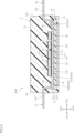
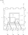
- FIG. 1 is a perspective view showing a semiconductor device according to a first embodiment of the present disclosure
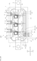
- FIG. FIG. 2 is a plan view of the semiconductor device shown in FIG. 1, and is a view through a resin member.
- FIG. 3 is a partially enlarged view enlarging a part of FIG.
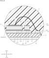
- FIG. 4 is a cross-sectional view taken along line IV-IV of FIG.
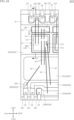
- FIG. 7 is a perspective view showing a state in which a drive device is attached to the semiconductor device shown in FIG. 1.
- FIG. 8 is a circuit diagram showing an example of the circuit configuration of the semiconductor device shown in FIG. 1.
- FIG. 9 is a flow chart showing an example of a method for manufacturing the semiconductor device shown in FIG. 10A and 10B are cross-sectional views showing steps according to an example of a method of manufacturing the semiconductor device shown in FIG. 11A and 11B are cross-sectional views showing steps according to an example of a method of manufacturing the semiconductor device shown in FIG. 12A and 12B are cross-sectional views showing steps according to an example of a method of manufacturing the semiconductor device shown in FIG. 13A and 13B are cross-sectional views showing steps according to an example of a method of manufacturing the semiconductor device shown in FIG. 14A and 14B are cross-sectional views showing steps according to an example of a method of manufacturing the semiconductor device shown in FIG.
- FIG. 15A and 15B are cross-sectional views showing steps according to an example of a method of manufacturing the semiconductor device shown in FIG. 16 is a partially enlarged plan view showing a semiconductor device according to a first modification of the first embodiment;
- FIG. 17 is a partially enlarged plan view showing a semiconductor device according to a second modification of the first embodiment;
- FIG. 18 is a partially enlarged plan view showing a semiconductor device according to a third modification of the first embodiment;
- FIG. 19 is a cross-sectional view along line XIX-XIX in FIG. 18.
- FIG. FIG. 20 is a plan view showing a semiconductor device according to a second embodiment of the present disclosure, and is a view through a resin member.
- FIG. 21 is a plan view showing a semiconductor device according to a third embodiment of the present disclosure, and is a view through a resin member.
- 22 is a circuit diagram showing an example of the circuit configuration of the semiconductor device shown in FIG. 21.
- FIG. FIG. 23 is a partially enlarged plan view showing a semiconductor device according to a fourth embodiment of the present disclosure, and is a view through a resin member. 24 is a cross-sectional view taken along line XXIV-XXIV of FIG. 23.
- FIG. 25 is a circuit diagram showing an example of the circuit configuration of the semiconductor device shown in FIG. 23.
- FIG. FIG. 26 is a circuit diagram showing an example of the circuit configuration of the semiconductor device according to the fifth embodiment of the present disclosure; FIG.
- FIG. 27 is a plan view showing a semiconductor device according to a sixth embodiment of the present disclosure, and is a view through a resin member.
- FIG. 28 is a plan view showing a semiconductor device according to a first modification of the sixth embodiment, and is a view through a resin member.
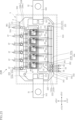
- FIG. 1 A semiconductor device A10 according to the first embodiment of the present disclosure will be described based on FIGS. 1 to 8.
- FIG. The semiconductor device A10 includes a plurality of semiconductor elements 11, a plurality of semiconductor elements 12, a support member 2, a plurality of terminals 3, a plurality of connection members 41-47, and a resin member 5.
- FIG. The plurality of terminals 3 includes power terminals 31 and 32 , signal terminals 33 , detection terminals 34 and 35 and temperature detection terminals 36 and 37 .
- the semiconductor device A10 is used with the driving device 7 attached.
- FIG. 1 is a perspective view showing the semiconductor device A10.
- FIG. 2 is a plan view of the semiconductor device A10.
- the outline of the resin member 5 is shown by an imaginary line (chain double-dashed line) through the resin member 5.
- FIG. 3 is a partially enlarged view enlarging a part of FIG.
- FIG. 4 is a cross-sectional view taken along line IV-IV of FIG.
- FIG. 5 is a cross-sectional view along line VV in FIG. 4 and 5, the connection members 41 to 47 are omitted.
- 6 is a cross-sectional view taken along line VI-VI of FIG. 3.
- FIG. FIG. 7 is a perspective view showing a state in which the driving device 7 is attached to the semiconductor device A10.
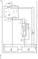
- FIG. 8 is a circuit diagram showing an example of the circuit configuration of the semiconductor device A10.
- the portion of the semiconductor device A10 covered with the resin member 5 has a rectangular shape when viewed in the thickness direction (also referred to as "planar view").
- the thickness direction of the semiconductor device A10 is assumed to be the z-direction, and the direction in which the power terminals 31 and 32 of the semiconductor device A10 protrude perpendicular to the z-direction (horizontal direction in FIG. 2) is the x-direction, the z-direction, and the x-direction.
- the direction orthogonal to (vertical direction in FIG. 2) is defined as the y direction.
- Each dimension of the semiconductor device A10 is not particularly limited.
- the plurality of semiconductor elements 11 are elements that exhibit electrical functions of the semiconductor device A10.
- Each semiconductor element 11 is configured using a semiconductor material mainly including SiC (silicon carbide), for example.
- the semiconductor material is not limited to SiC, and may be Si (silicon), GaAs (gallium arsenide), GaN (gallium nitride), or the like.
- Each semiconductor element 11 is a switching element such as a MOSFET (Metal-Oxide-Semiconductor Field-Effect Transistor).
- Each semiconductor element 11 is not limited to a MOSFET, and may be a field effect transistor including a MISFET (Metal-Insulator-Semiconductor FET), or a bipolar transistor such as an IGBT (Insulated Gate Bipolar Transistor).
- the plurality of semiconductor elements 11 are, for example, n-channel MOSFETs, and are the same element.
- Each semiconductor element 11 may be a p-channel MOSFET.
- the plurality of semiconductor elements 11 are arranged at regular intervals in the x direction and connected in parallel.
- the semiconductor device A10 includes five semiconductor elements 11, as shown in FIG.
- the number of semiconductor elements 11 is not limited to this, and can be freely set according to the performance required of the semiconductor device A10.
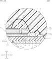
- Each semiconductor element 11 is bonded onto the support member 2 with a conductive bonding material 110 .
- Conductive bonding material 110 is, for example, solder, silver paste, or sintered metal.
- Each semiconductor element 11 has an element main surface 11a and an element back surface 11b.
- the element main surface 11a and the element back surface 11b face opposite sides in the z-direction.
- the element principal surface 11a faces the z-direction z2 side.
- the element back surface 11b faces the z-direction z1 side.
- the element back surface 11 b faces the support member 2 .
- Each semiconductor element 11 also has a first electrode 111 , a second electrode 112 and a third electrode 113 .
- the first electrode 111 and the second electrode 112 are arranged on the element main surface 11a.
- the first electrode 111 is larger than the second electrode 112 in plan view.
- the third electrode 113 is arranged on the element back surface 12b.
- the third electrode 113 extends over the entire surface (or substantially the entire surface) of the element back surface 11b.
- the constituent material of the first electrode 111, the second electrode 112, and the third electrode 113 is not limited, it is Al in this embodiment.
- the first electrode 111 is the source electrode
- the second electrode 112 is the gate electrode
- the third electrode 113 is the drain electrode.
- the third electrode 113 is conductively joined to a part of the support member 2 (a conductor layer 223 of the main surface metal layer 22 to be described later) via the conductive joining material 110 .
- the third electrode 113 contacts the conductive bonding material 110 .
- a metal plate 19 is joined to the first electrode 111 of each semiconductor element 11 .
- the metal plate 19 is arranged such that it is electrically connected to the first electrode 111 and heat from the semiconductor element 11 is appropriately conducted. Connection members 41 , 44 to 47 are joined to the metal plate 19 .
- Metal plate 19 contains a third metal.
- the third metal is Cu.
- the metal plate 19 is, for example, a clad material obtained by bonding a thin plate member made of Al to one surface of a plate member made of Cu.
- the metal plate 19 is joined to the first electrode 111 by, for example, solid-phase diffusion joining, with the Al surface facing the first electrode 111 (Al).
- the configuration of the metal plate 19 and the bonding method to the first electrode 111 are not limited.
- the metal plate 19 may be formed by forming an Al layer on one surface of a plate member made of Cu by sputtering or the like.
- the plurality of semiconductor elements 12 are diodes such as Schottky barrier diodes, for example. Each semiconductor element 12 is connected in anti-parallel with respect to each semiconductor element 11, as shown in FIG.
- Each semiconductor element 12 is bonded onto the support member 2 with a conductive bonding material 120 .
- Conductive bonding material 120 is, for example, solder, silver paste, or sintered metal.
- the number of semiconductor elements 12 corresponds to the number of semiconductor elements 11 . Note that the semiconductor device A10 does not have to include each semiconductor element 12 .
- Each semiconductor element 12 has an element main surface 12a and an element back surface 12b.
- the element main surface 12a and the element back surface 12b face opposite sides in the z-direction.
- the element main surface 12a faces the z-direction z2 side.
- the element back surface 12b faces the z-direction z1 side.
- the element back surface 12 b faces the support member 2 .
- Each semiconductor element 12 has an anode electrode 121 and a cathode electrode 122 .
- the anode electrode 121 is arranged on the element main surface 12a.
- the cathode electrode 122 is arranged on the element back surface 12b.
- the cathode electrode 122 is electrically connected to a part of the support member 2 (a conductor layer 223 of the main surface metal layer 22 described later) through the conductive bonding material 120 .
- Cathode electrode 122 is in contact with conductive bonding material 120 .
- the support member 2 is a member that supports a plurality of semiconductor elements 11 and 12, respectively, and forms a conduction path between each semiconductor element 11 and a plurality of terminals 3.
- the support member 2 includes an insulating substrate 21 , a main surface metal layer 22 and a back surface metal layer 23 .
- Insulating substrate 21 is, for example, flat and has electrical insulation.
- a constituent material of the insulating substrate 21 is, for example, ceramics having excellent thermal conductivity, and in this embodiment, it is Al 2 O 3 (aluminum oxide).
- the constituent material of the insulating substrate 21 is not limited, and may be other ceramics such as AlN (aluminum nitride) and SiN (silicon nitride).
- the constituent material of the insulating substrate 21 is not limited to ceramics, and may be Si or synthetic resin.
- the insulating substrate 21 may be made of any material as long as it has insulating properties and can withstand the heat generated by the semiconductor element 11 .
- the insulating substrate 21 has a principal surface 211 and a back surface 212 .
- the main surface 211 and the back surface 212 face opposite sides in the z-direction.
- the main surface 211 faces the z-direction z2 side.
- the back surface 212 faces the z-direction z1 side.
- the main surface metal layer 22 is formed on the main surface 211 of the insulating substrate 21 .
- a constituent material of the main surface metal layer 22 is a metal, and examples thereof include Cu, an alloy containing Cu, and the like. In addition, the constituent material of the main surface metal layer 22 is not limited.
- Main surface metal layer 22 is formed by plating, for example. Note that the method for forming the main surface metal layer 22 is not limited.
- the main surface metal layer 22 is covered with the resin member 5 .
- the main surface metal layer 22 includes conductor layers 221 to 225 and a plurality of conductor layers 226 and 227, respectively. Each conductor layer 221-227 is spaced apart from each other.
- the conductor layer 221 includes strip portions 221a and terminal joint portions 221b.
- the band-shaped portion 221a extends along the x-direction, and a plurality of connecting members 41 and connecting members 42 are respectively joined.
- the terminal joint portion 221b is connected to the end portion of the strip portion 221a on the x-direction x2 side, and is joined to a portion of the power terminal 32 (a pad portion 321 described later).
- the conductor layer 222 includes strip portions 222a and terminal joint portions 222b.
- the band-shaped portion 222a extends along the x-direction, and a plurality of connection members 43 are joined to each of the band-shaped portions 222a.
- the terminal joint portion 222b is connected to the end portion of the strip portion 222a on the x-direction x1 side, and is joined to a part of the signal terminal 33 (a pad portion 331 described later).
- the conductor layer 223 includes a strip-shaped portion 223a and a terminal joint portion 223b.
- the band-shaped portion 223a extends along the x-direction, and a plurality of semiconductor elements 11 and 12 are bonded to each of them. Heat from each semiconductor element 11 is appropriately transmitted to the belt-like portion 223a (conductor layer 223) through the conductive bonding material 110. As shown in FIG.
- the plurality of semiconductor elements 11 bonded to the band-shaped portion 223a are arranged in the direction (x-direction) in which the band-shaped portion 223a extends.
- the terminal joint portion 223b is connected to the end portion of the strip portion 223a on the x-direction x1 side, and is joined to a portion of the power terminal 31 (a pad portion 311 described later).
- the conductor layer 223 is electrically connected to the third electrode 113 (drain electrode) of each semiconductor element 11 through each conductive bonding material 110, and is connected to each conductive bonding material 120. to the cathode electrode 122 of each semiconductor element 12 through the . That is, the third electrode 113 of each semiconductor element 11 and the cathode electrode 122 of each semiconductor element 12 are electrically connected through the conductor layer 223 .
- the conductor layer 224 includes strip portions 224a and terminal joint portions 224b.
- the band-shaped portion 224a extends along the x-direction, and a plurality of connection members 44 are joined to each of the strip-shaped portions 224a.
- the terminal joint portion 224b is connected to the end portion of the strip portion 224a on the x-direction x1 side, and is joined to a part of the detection terminal 35 (a pad portion 351 described later).
- connection member 42 is joined to the conductor layer 225 .
- a part of the detection terminal 34 (a pad portion 341 to be described later) is joined to the conductor layer 225 .
- the plurality of band-shaped portions 221a, 222a, 223a, and 224a are arranged in the y direction and overlap each other when viewed in the y direction.
- the arrangement in the y-direction of the plurality of band-shaped portions 221a, 222a, 223a, and 224a is not particularly limited.
- the belt-shaped portion 224a, the belt-shaped portion 222a, the belt-shaped portion 221a, and the belt-shaped portion 223a are arranged in this order from the y-direction y1 side toward the y-direction y2 side.
- the band-shaped portion 221a is arranged between the band-shaped portion 222a and the band-shaped portion 223a in the y direction, and the band-shaped portion 222a is arranged between the band-shaped portion 221a and the band-shaped portion 224a in the y-direction.
- the band-shaped portion 223a is arranged on the opposite side of the band-shaped portion 222a in the y direction with the band-shaped portion 221a interposed therebetween.
- the conductor layer 225 is arranged on the x-direction x1 side of the terminal joint portion 222b of the conductor layer 222 .
- Each of the plurality of conductor layers 226 and 227 is arranged on the y-direction y2 side of the strip-shaped portion 223a of the conductor layer 223.
- the main surface metal layer 22 includes the same number of conductor layers 226 and conductor layers 227 as the semiconductor element 11 (five in this embodiment).
- the conductor layers 226 and the conductor layers 227 are alternately arranged along the x-direction.
- a connection member 46 is joined to each conductor layer 226 .
- a part of the temperature detection terminal 36 (a pad portion 361 to be described later) is joined to each conductor layer 226 .
- a connection member 47 is joined to each conductor layer 227 .
- a part of the temperature detection terminal 37 (a pad portion 371 to be described later) is joined to each conductor layer 227 .
- each of the conductor layers 221 to 227 are not limited to those described above, and can be appropriately designed according to the arrangement position of each terminal 3 and the like.
- the back metal layer 23 is formed on the back surface 212 of the insulating substrate 21 .
- the constituent material of the back surface metal layer 23 is a metal, and examples thereof include Cu, an alloy containing Cu, and the like. In addition, the said constituent material is not limited.
- Back surface metal layer 23 is formed, for example, by electroless plating. The method for forming the back metal layer 23 is not limited. As shown in FIGS. 4 and 5, the back metal layer 23 has a surface facing the z-direction z1 exposed from the resin member 5 . Note that the surface facing the z-direction z1 side may be covered with the resin member 5 . Moreover, the support member 2 does not have to include the back metal layer 23 . In this case, the back surface 212 of the insulating substrate 21 may be covered with the resin member 5 or may be exposed from the resin member 5 .
- Each terminal 3 is joined to the main surface metal layer 22 inside the resin member 5 .
- Each terminal 3 protrudes from the insulating substrate 21 when viewed in the z direction. A part of each terminal 3 is exposed from the resin member 5 .
- Each terminal 3 is composed of, for example, the same lead frame.
- Each terminal 3 is made of metal, preferably Cu or Ni, or an alloy thereof, 42 alloy, or the like.
- the power terminal 31 is the drain terminal in the semiconductor device A10.
- the power terminal 31 is a plate-like member.
- the power terminal 31 is electrically connected to the third electrode 113 (drain electrode) of each semiconductor element 11 via the conductor layer 223 and the conductive bonding material 110 .
- the power terminal 31 includes a pad portion 311 and a terminal portion 312 .
- the pad portion 311 is covered with the resin member 5 .
- the pad portion 311 is bonded to the conductor layer 223 . This bonding may be performed by any technique such as bonding using a conductive bonding material (solder, silver paste, sintered metal, etc.), laser bonding, or ultrasonic bonding.
- the terminal portion 312 is exposed from the resin member 5 . As shown in FIG. 2, the terminal portion 312 extends from the resin member 5 in the x direction x1 when viewed in the z direction.
- the surface of terminal portion 312 may be plated with silver, for example.
- the power terminal 32 is the source terminal in the semiconductor device A10.
- the power terminal 32 is a plate-like member.
- the power terminal 32 is electrically connected to the first electrode 111 (source electrode) of each semiconductor element 11 via the conductor layer 221 , the plurality of connection members 41 and the metal plate 19 .
- the power terminal 32 includes a pad portion 321 and a terminal portion 322 .
- the pad portion 321 is covered with the resin member 5 .
- the pad portion 321 is bonded to the conductor layer 221 . This bonding may be performed by any method such as bonding using a conductive bonding material, laser bonding, or ultrasonic bonding.
- the terminal portion 322 is exposed from the resin member 5 . As shown in FIG. 2, the terminal portion 322 extends from the resin member 5 in the x direction x2 when viewed in the z direction.
- the surface of terminal portion 322 may be plated with silver, for example.
- the signal terminal 33 is a gate terminal in the semiconductor device A10.
- the signal terminal 33 is electrically connected to the second electrode 112 (gate electrode) of each semiconductor element 11 via the conductor layer 222 and the plurality of connecting members 43 .
- a drive signal for on/off control of each semiconductor element 11 is input to the signal terminal 33 .
- a drive circuit DR is connected to the signal terminal 33 as shown in FIG.
- the drive circuit DR generates a drive signal that controls the switching operation of each semiconductor element 11 .
- a drive signal is input to the signal terminal 33 from the drive circuit DR.
- the drive circuit DR shown in FIG. 8 is an example and is not limited to the illustrated circuit configuration.
- the signal terminal 33 includes a pad portion 331 and a terminal portion 332 .
- the pad portion 331 is covered with the resin member 5 .
- the pad portion 331 is bonded to the conductor layer 222 . This bonding may be performed by any method such as bonding using a conductive bonding material, laser bonding, or ultrasonic bonding.
- the terminal portion 332 is exposed from the resin member 5 .
- the terminal portion 332 is L-shaped when viewed in the x direction.
- the detection terminal 34 is a source sense terminal in the semiconductor device A10.
- the detection terminal 34 is electrically connected to the first electrode 111 (source electrode) of the semiconductor element 11 via the conductor layer 225 , the connection member 42 , the conductor layer 221 , the plurality of connection members 41 and the metal plate 19 .
- a drive circuit DR is connected to the detection terminal 34 as shown in FIG.
- the voltage applied to the detection terminal 34 is input to the drive circuit DR as a feedback signal.
- the detection terminal 34 includes a pad portion 341 and a terminal portion 342 .
- the pad portion 341 is covered with the resin member 5 .
- the pad portion 341 is bonded to the conductor layer 225 . This bonding may be performed by any method such as bonding using a conductive bonding material, laser bonding, or ultrasonic bonding.
- the terminal portion 342 is exposed from the resin member 5 .
- the terminal portion 342 is L-shaped when viewed in the x direction.
- the detection terminal 35 is a source sense terminal in the semiconductor device A10.
- the detection terminal 35 is electrically connected to the first electrode 111 (source electrode) of each semiconductor element 11 via the conductor layer 224 , the plurality of connecting members 44 and the metal plate 19 .
- a Miller clamp circuit MC outside the semiconductor device A10 is connected between the detection terminal 35 and the signal terminal 33, as shown in FIG.
- the Miller clamp circuit MC is a circuit for preventing malfunction (gate erroneous turn-on) of each semiconductor element 11, and includes, for example, a MOSFET as shown in FIG.
- the source terminal of the MOSFET is connected to the sense terminal 35 and the drain terminal of the MOSFET is connected to the signal terminal 33 .
- the voltage between the gate and source of the semiconductor element 11 is forced to 0 (zero) V (or approximately 0 V) or a negative bias voltage. Eliminates the gate potential rise of element 11 .
- the detection terminal 35 includes a pad portion 351 and a terminal portion 352 .
- the pad portion 351 is covered with the resin member 5 .
- the pad portion 351 is bonded to the conductor layer 224 . This bonding may be performed by any method such as bonding using a conductive bonding material, laser bonding, or ultrasonic bonding.
- the terminal portion 352 is exposed from the resin member 5 . As shown in FIG. 4, the terminal portion 352 is L-shaped when viewed in the x direction.
- the detection terminal 34, the signal terminal 33, and the detection terminal 35 are arranged in this order from the x direction x1 side to the x2 side along the x direction, as shown in FIGS. overlap in the x-direction view.
- the detection terminal 34, the signal terminal 33, and the detection terminal 35 protrude from the resin side surface 533 on the y-direction y1 side.
- a plurality of temperature detection terminals 36 and 37 are terminals for detecting the temperature of the semiconductor element 11 respectively.
- One temperature detection terminal 36 and one temperature detection terminal 37 are provided for one semiconductor element 11 .
- the semiconductor device A10 has five semiconductor elements 11, and therefore has five temperature detection terminals 36 and five temperature detection terminals 37.
- Each temperature detection terminal 36 is joined to the conductor layer 226 respectively.
- Each temperature detection terminal 36 is electrically connected to the connection member 46 via the conductor layer 226 .
- Each temperature detection terminal 37 is joined to the conductor layer 227 .
- Each temperature detection terminal 37 is electrically connected to the connection member 47 via the conductor layer 227 .
- the temperature detection terminal 36 includes a pad portion 361 and a terminal portion 362 .
- the pad portion 361 is covered with the resin member 5 .
- the pad portion 361 is bonded to the conductor layer 226 . This bonding may be performed by any method such as bonding using a conductive bonding material, laser bonding, or ultrasonic bonding.
- the terminal portion 362 is exposed from the resin member 5 . As shown in FIG. 4, the terminal portion 362 is L-shaped when viewed in the x direction.
- the temperature detection terminal 37 includes a pad portion 371 and a terminal portion 372 .
- the pad portion 371 is covered with the resin member 5 .
- the pad portion 371 is bonded to the conductor layer 227 .
- This bonding may be performed by any method such as bonding using a conductive bonding material, laser bonding, or ultrasonic bonding.
- the terminal portion 372 is exposed from the resin member 5 .
- the terminal portion 372 is L-shaped when viewed in the x direction.
- the plurality of temperature detection terminals 36 and the plurality of temperature detection terminals 37 are alternately arranged along the x-direction as shown in FIGS. 2 and 3, and overlap when viewed in the x-direction as shown in FIG. .
- Each of the temperature detection terminals 36 and 37 protrudes from the resin side surface 534 on the y-direction y2 side.
- Each of the plurality of connection members 41-45 conducts between two separated parts.
- Each connection member 41-45 is a so-called bonding wire.
- each connection member 41-45 is formed by wedge bonding.
- each connection member 41 to 45 may be formed by ball bonding.
- the constituent material of each connection member 41 to 45 is, for example, Al, Au, Cu, or an alloy containing any of these, and is not limited. In the present embodiment, a case where the constituent material of each of the connection members 41 to 45 is Cu will be described.
- Each of the plurality of connection members 41 has one end joined to the metal plate 19 and the other end joined to the conductor layer 221 .
- Each connecting member 41 electrically connects the first electrode 111 (source electrode) of each semiconductor element 11 and the conductor layer 221 .
- connection member 42 has one end joined to the conductor layer 221 and the other end joined to the conductor layer 225 .
- the connection member 42 electrically connects the conductor layer 221 and the conductor layer 225 .
- the other end of the connection member 42 may be joined to the pad portion 341 of the detection terminal 34 instead of being joined to the conductor layer 225 .
- Each of the plurality of connection members 43 has one end joined to the second electrode 112 (gate electrode) of each semiconductor element 11 and the other end joined to the conductor layer 222 .
- Each connection member 43 electrically connects each second electrode 112 and the conductor layer 222 .
- Each of the plurality of connection members 44 has one end joined to the metal plate 19 and the other end joined to the conductor layer 224 .
- Each connection member 44 electrically connects the first electrode 111 (source electrode) of each semiconductor element 11 and the conductor layer 224 .
- Each connection member 44 is a sense line Kelvin-connected to the first electrode 111 (source electrode) of each semiconductor element 11 .
- Each of the plurality of connection members 45 has one end joined to the metal plate 19 and the other end joined to the anode electrode 121 of each semiconductor element 12 .
- Each connecting member 45 electrically connects the first electrode 111 (source electrode) of each semiconductor element 11 and the anode electrode 121 of each semiconductor element 12 .
- connection members 46 and 47 are members for detecting the temperature of the semiconductor element 11 respectively.
- Each of the connection members 46 and 47 is formed by the method of forming a bonding wire, like the connection members 41-45.
- each connecting member 46, 47 is formed by wedge bonding.
- the connection members 46 and 47 may be formed by ball bonding.
- Each connecting member 46 has one end joined to the metal plate 19 and the other end joined to the conductor layer 226 .
- Each connecting member 47 has one end joined to the metal plate 19 and the other end joined to the conductor layer 227 .
- Both connection members 46 and 47 are directly joined to the metal plate 19 . That is, the connection members 46 and 47 and the metal plate 19 are in direct contact with each other without any other member interposed therebetween.
- the connection member 46 and the connection member 47 are joined apart from each other.
- the constituent material of the connection member 46 is the first metal.
- the first metal is Cu, which is the same as the third metal.
- a constituent material of the connection member 47 is a second metal having a thermoelectric power different from that of the first metal.
- Thermoelectric power is the thermoelectromotive force per 1K when a temperature difference is applied to both ends of a conductive substance.
- the second metal is constantan (alloy of Cu and Ni: 55Cu-45Ni).
- the connection member 46, the metal plate 19 (Cu), and the connection member 47 (constantan) function as a thermocouple.
- Thermocouples with Cu and constantan are commonly known as T-type thermocouples.
- a contact 47a between the connecting member 47 and the metal plate 19 corresponds to a temperature measuring contact (thermal contact) of the thermocouple.
- the contact between the connection member 46 and the conductor layer 226 and the contact between the connection member 47 and the conductor layer 227 correspond to the reference junction (cold junction) of the thermocouple.
- a voltage is generated across the reference junction according to the temperature difference between the reference junction and the temperature measuring junction.
- Temperature detection terminals 36 and 37 output the voltage between the reference contacts to drive device 7 as a signal for detecting the temperature of semiconductor element 11 .
- the resin member 5 is an electrically insulating semiconductor sealing material.
- the resin member 5 covers the plurality of semiconductor elements 11, the plurality of semiconductor elements 12, the insulating substrate 21, the main surface metal layer 22, the plurality of connection members 41 to 47 as a whole, and part of each terminal 3.
- a constituent material of the resin member 5 is, for example, an epoxy resin.
- the constituent material of the resin member 5 is not limited.
- Resin member 5 is formed, for example, by transfer molding using a mold. In addition, the formation method of the resin member 5 is not limited. As shown in FIGS. 2, 4 and 5, the resin member 5 has a resin main surface 51, a resin back surface 52 and a plurality of resin side surfaces 531-534.
- the resin main surface 51 and the resin back surface 52 face opposite sides in the z-direction.
- the resin main surface 51 faces the z-direction z2 side
- the resin back surface 52 faces the z-direction z1 side.
- the back surface metal layer 23 is exposed from the resin back surface 52, and the resin back surface 52 and the surface of the back surface metal layer 23 facing the z-direction z1 side are flush with each other.
- Each of the plurality of resin side surfaces 531 to 534 is connected to both the resin main surface 51 and the resin back surface 52 and is sandwiched between them. As shown in FIG. 2, the two resin side surfaces 531 and 532 face opposite sides in the x direction.
- the resin side surface 531 is a surface that is arranged on the x-direction x1 side and faces the x-direction x1 side.
- the resin side surface 532 is a surface that is arranged on the x-direction x2 side and faces the x-direction x2 side.
- the two resin side surfaces 533, 534 face opposite sides in the y direction.
- the resin side surface 533 is a surface arranged on the y-direction y1 side and facing the y-direction y1 side.
- the resin side surface 534 is a surface that is arranged on the y-direction y2 side and faces the y-direction y2 side.
- the resin side surfaces 531 to 534 each have a surface connected to the resin main surface 51 and inclined so as to approach each other toward the resin main surface 51 . That is, the portion of the resin member 5 surrounded by the inclined surfaces connected to the resin main surface 51 has a tapered shape in which the cross-sectional area in the xy plane becomes smaller toward the resin main surface 51 . Further, the resin side surfaces 531 to 534 each have surfaces connected to the resin back surface 52 and inclined so as to approach each other toward the resin back surface 52 . In other words, the portion of the resin member 5 that is connected to the resin main surface 51 and surrounded by the inclined surfaces has a tapered shape in which the cross-sectional area in the xy plane becomes smaller toward the resin back surface 52 . Note that the shape of the resin member 5 shown in FIGS. 1 to 5 is an example. The shape of the resin member 5 is not limited to the illustrated shape.
- the driving device 7 is a device that drives the semiconductor device A10, and is attached on the z-direction z2 side of the semiconductor device A10, as shown in FIG.
- the driving device 7 includes a substrate 71, terminals 723, 724, 725, and a plurality of terminals 721, 722, respectively.
- Substrate 71 is, for example, flat and has electrical insulation.
- the constituent material of the substrate 71 is not limited.
- Substrate 71 has a major surface 711 and a back surface 712 .
- the main surface 211 and the back surface 712 face opposite sides in the z-direction.
- the main surface 711 faces the z-direction z2 side.
- the back surface 712 faces the z-direction z1 side. Wiring is formed on the main surface 711, and external connectors, a large number of electronic components, and the like are mounted. However, in FIG. there is
- Each of the terminals 721 to 725 is a cylindrical metal member, and is arranged to be inserted through a through hole penetrating from the main surface 711 to the back surface 712 of the substrate 71 in the z direction.
- Each of terminals 721 to 725 is electrically connected to wiring formed on main surface 711 .
- the terminal portions 332, 342, 352, 362, and 372 of the terminals 33 to 37 of the semiconductor device A10 are inserted through the terminals 721 to 725, respectively, and joined by soldering, for example.
- the signal terminal 33 is joined to the terminal 723 .
- the detection terminal 34 is joined to the terminal 724 .
- the detection terminal 35 is joined to the terminal 725 .
- the temperature detection terminals 36 five terminals 721 are arranged, and the temperature detection terminals 36 are joined to the terminals 721, respectively. Since the temperature detection terminal 36 is conductively connected to the connection member 46 via the conductor layer 226 , the terminal 721 is conductively connected to the connection member 46 . As with the temperature detection terminals 37, five terminals 722 are arranged, and the temperature detection terminals 37 are joined to the terminals 722, respectively. Since the temperature detection terminal 37 is conductively connected to the connecting member 47 via the conductor layer 227 , the terminal 722 is conductively connected to the connecting member 47 .
- the drive device 7 includes a plurality of relative temperature detection units 73, a plurality of reference junction compensation units 74, an overheat protection unit 75, and a drive control unit 76 as functional configurations.
- the drive control unit 76 is a functional configuration that controls the switching operation of each semiconductor element 11, and is realized by a gate drive IC, for example.
- the drive control unit 76 includes a drive circuit DR, a Miller clamp circuit MC, and the like.
- the drive control unit 76 generates a drive signal based on a control signal input from the outside, and outputs the drive signal to the semiconductor device A10 via the terminal 723 .
- the semiconductor device A10 receives a drive signal from the signal terminal 33 connected to the terminal 723 and controls the switching operation of each semiconductor element 11 . Further, the drive control unit 76 receives a signal from the detection terminal 34 of the semiconductor device A10 through a terminal 724 and receives a signal from the detection terminal 35 through a terminal 725 . Note that the specific circuit configuration and mode of the drive control unit 76 are not limited.
- the relative temperature detection section 73 and the reference junction compensation section 74 are functional components for detecting the temperature of the semiconductor element 11 .
- Five relative temperature detectors 73 and five reference junction compensators 74 are provided according to the number of semiconductor elements 11 of the semiconductor device A10.
- Each relative temperature detection unit 73 receives a voltage from the pair of temperature detection terminals 36 and 37 of the semiconductor device A10 via a pair of terminals 721 and 722 .
- This voltage is the voltage across the reference junction of the thermocouple having the connecting member 46 and the metal plate 19 and the connecting member 47, and is the voltage corresponding to the temperature difference between the reference junction and the temperature measuring junction. That is, the voltage is a voltage corresponding to the relative temperature of the semiconductor element 11 with respect to the temperature of the reference junction.
- Each relative temperature detector 73 detects the relative temperature of the corresponding semiconductor element 11 based on the input voltage.
- Each reference junction compensator 74 converts the relative temperature detected by the corresponding relative temperature detector 73 into an absolute temperature.
- Each reference junction compensator 74 includes a temperature detector having a diode, for example, arranged adjacent to corresponding terminals 721 and 722 .
- the temperature detection unit may have a temperature sensor such as a thermistor.
- the temperature detection terminals 36 and 37 joined to the terminals 721 and 722 are joined to the conductor layers 226 and 227, respectively.
- the temperature detector indirectly detects the temperature of the reference junction of the thermocouple by detecting the temperatures of the terminals 721 and 722 .
- the reference junction compensation section 74 adds the temperature of the reference junction detected by the temperature detection section to the relative temperature detected by the corresponding relative temperature detection section 73, thereby converting the temperature into an absolute temperature.
- the reference junction compensator 74 outputs the absolute temperature of the corresponding semiconductor element 11 to the overheat protector 75 .
- the specific circuit configurations of the relative temperature detection section 73 and the reference junction compensation section 74 are not limited.
- the following configuration may be used. That is, the relative temperature detector 73 transmits the voltage between the pair of terminals 721 and 722 to the reference junction compensator 74 as a voltage corresponding to the relative temperature of the corresponding semiconductor element 11 . Then, the reference junction compensator 74 converts the voltage corresponding to the temperature of the reference junction detected by the temperature detector into a voltage corresponding to the thermoelectromotive force of the thermocouple, and adds the voltage to the voltage transmitted from the relative temperature detector 73 . and output to the overheat protection unit 75 . As a result, a voltage corresponding to the absolute temperature of the semiconductor element 11 is input to the overheat protection unit 75 .
- the overheat protection unit 75 detects an overheating abnormality of the corresponding semiconductor element 11 based on the absolute temperature input from each reference junction compensation unit 74 .
- the overheat protection unit 75 outputs an abnormality detection signal to the drive control unit 76 when the absolute temperature input from each reference junction compensation unit 74 becomes equal to or higher than the threshold temperature.
- the drive control unit 76 stops the drive of the semiconductor device A10 by stopping the output of the drive signal.
- a specific circuit configuration of the overheat protection unit 75 is not limited.
- the overheat protection unit 75 may include a comparator that generates an abnormality detection signal when the voltage corresponding to the absolute temperature input from the reference junction compensating unit 74 exceeds the voltage corresponding to the threshold temperature. .
- FIG. 9 is a flow chart showing an example of a method for manufacturing the semiconductor device A10.
- 10 to 15 are diagrams showing processes according to an example of the method of manufacturing the semiconductor device A10.
- 10 to 15 are sectional views corresponding to FIG. 4.
- FIG. Note that the x-direction, y-direction, and z-direction shown in FIGS. 10 to 15 are the same directions as in FIGS.
- the method of manufacturing the semiconductor device A10 includes a supporting member forming step (S1), a lead frame bonding step (S2), a semiconductor element mounting step (S3), a wire forming step (S4), a resin forming step ( S5), and a frame cutting step (S6).
- the supporting member forming step (S1) is a step of forming the supporting member 2.
- an insulating substrate 91 is prepared (S11).
- the insulating substrate 91 is made of ceramics, for example, and has a main surface 911 and a back surface 912 facing opposite to each other in the z-direction.
- the main surface metal layer 22 is formed on the main surface 911 of the insulating substrate 91 (S12).
- the main surface metal layer 22 is formed by forming a base layer covering the entire main surface 911 by, for example, electroless plating or sputtering, forming a mask, forming a plating layer by electroplating, and etching to form the base layer. It is formed by removing parts.
- the back surface metal layer 23 is formed on the back surface 912 of the insulating substrate 91 (S13).
- Back surface metal layer 23 is formed, for example, by electroless plating.
- a DBC (Direct Bonding Copper) substrate in which Cu foil is bonded to the main surface 911 and the back surface 912 of the insulating substrate 91 , the Cu foil on the main surface 911 side is patterned so that the main surface metal Layer 22 and backside metal layer 23 may be formed.
- the insulating substrate 91 is cut (S14).
- the insulating substrate 21 is formed by cutting the insulating substrate 91 .
- the support member 2 is formed by the above.
- the lead frame 92 that will become each terminal 3 is prepared.
- the lead frame 92 includes a portion to be each terminal 3 and further has a frame to which a plurality of terminals 3 are connected. Note that the shape of the lead frame 92 and the like are not limited at all.
- a conductive bonding paste is placed at the position where each terminal 3 of the main surface metal layer 22 is to be bonded, and as shown in FIG. do.
- the portion of the lead frame 92 that will become the detection terminal 35 is joined to the conductor layer 224 .
- a portion of the lead frame 92 that will become the detection terminal 36 is joined to the conductor layer 226 . Note that the joining method of the lead frame 92 is not limited.
- the conductive bonding paste 93 is placed on the regions of the conductor layer 223 where the semiconductor elements 11 and 12 are to be placed.
- Conductive bonding paste 93 is, for example, solder, silver paste, or sintered metal.
- the plurality of semiconductor elements 11 and the plurality of semiconductor elements 12 are adhered to the conductive bonding paste 93, heated, and then cooled.
- the conductive bonding paste 93 interposed between the conductor layer 223 and the semiconductor element 11 becomes the conductive bonding material 110, and the semiconductor element 11 is bonded to the conductor layer 223 via the conductive bonding material 110. be.
- the semiconductor element 11 has the metal plate 19 bonded in advance to the first electrode 111 .
- the conductive bonding paste 93 interposed between the conductor layer 223 and the semiconductor element 12 becomes the conductive bonding material 120, and the semiconductor element 12 is bonded to the conductor layer 223 via the conductive bonding material 120. .
- connection members 41 to 46 are formed by wedge bonding (S41).
- a connection member 41 is formed to connect the metal plate 19 joined to the first electrode 111 of the semiconductor element 11 and the conductor layer 221 .
- a connection member 43 is formed to connect the second electrode 112 of the semiconductor element 11 and the conductor layer 222 .
- a connection member 44 is formed to connect the metal plate 19 and the conductor layer 224 .
- a connection member 45 is formed to connect the metal plate 19 and the anode electrode 121 of the semiconductor element 12 .
- a connection member 46 is formed to connect the metal plate 19 and the conductor layer 226 . Also, although not shown in FIG.
- connection member 42 is formed to connect the conductor layer 221 and the conductor layer 225 . Since the connecting member 46 is made of Cu, which is the same material as the connecting members 41 to 45, the connecting member 46 is formed in the same process as the connecting members 41 to 45. FIG. The order of forming the connection members 41 to 46 is not limited. Next, as shown in FIG. 15, connecting members 47 are formed by wedge bonding (S42). A connection member 47 is formed to connect the metal plate 19 and the conductor layer 227 . The connection member 46 is formed in a process different from that of the connection members 41 to 46 because the material of the connection member 46 is different from that of the connection members 41 to 46 .
- connection member 47 is formed by the same method using the same equipment, except that the wire material used is different from the connection members 41 to 46 .
- the connection member 47 may be formed before the connection members 41 to 46 are formed.
- the connecting member 46 and the connecting member 47 are joined to the metal plate 19 to form a thermocouple.
- the resin forming step (S5) for example, a part of the lead frame 92, a part of the support member 2, the plurality of semiconductor elements 11 and 12, and the plurality of connection members 41 to 47 are surrounded by molds. Next, a liquid resin material is injected into the space defined by the mold. Then, the resin member 5 is obtained by curing the resin material.
- each semiconductor element 11 has a metal plate 19 joined to the first electrode 111 and one end of each of the connection members 46 and 47 joined to the metal plate 19 .
- a constituent material of the connection member 46 is the first metal, which is the same metal as the third metal that is the constituent material of the metal plate 19 .
- the constituent material of the connecting member 47 is a second metal having a thermoelectric power different from that of the first metal.
- the connection member 46, the metal plate 19, and the connection member 47 function as a thermocouple, and the temperature can be detected by using the junction 47a between the connection member 47 and the metal plate 19 as a thermocouple junction.
- the contact 47a is in contact with the metal plate 19 through which the heat from the semiconductor element 11 is properly conducted.
- the semiconductor device A10 can detect the temperature of each semiconductor element 11 with higher accuracy than when the temperature sensor is arranged near the semiconductor element 11 . Therefore, the semiconductor device A10 can improve the accuracy of the detected temperature of each semiconductor element 11 without forming a temperature sensor inside each semiconductor element 11 .
- the first metal and the third metal are Cu, and the second metal is constantan. Therefore, the connection member 46, the metal plate 19 (Cu), and the connection member 47 (constantan) function as a T-type thermocouple.
- the connecting members 46 and 47 are formed by the bonding wire forming method, similarly to the connecting members 41 to 45 . Therefore, the connection members 46 and 47 can be formed by the same method using the same equipment as the connection members 41-45. In particular, the connection member 46 can be formed in the same process as the connection members 41 to 45 because the constituent material thereof is Cu, which is the same as that of the connection members 41 to 45 .
- the metal plate 19 is joined to the first electrode 111 of each semiconductor element 11 .
- the semiconductor element 11 is protected from impact when the connecting members 41, 44 to 47 are wedge-bonded.
- the drive device 7 includes the relative temperature detection section 73 and the reference junction compensation section 74 . Therefore, the driving device 7 can convert the relative temperature of each semiconductor element 11 detected by the thermocouple composed of the connection member 46, the metal plate 19, and the connection member 47 into an absolute temperature and use it for overheat protection.
- the first metal that is the constituent material of the connection member 46 is Cu and the second metal that is the constituent material of the connection member 47 is constantan, but the present invention is not limited to this.
- the first metal and the second metal may be metals having different electrolytic capacities.
- the first metal may be Cu and the second metal may be Al.
- Cu and Al have the same polarity of electrolytic capacity, but different electrolytic capacities. Therefore, the connection member 46 and the metal plate 19 (Cu) and the connection member 47 (Al) function as a thermocouple.
- Al is commonly used as a bonding wire, and can be easily obtained at a low cost compared to a constantan wire.
- the combination of the first metal and the second metal may be Chromel® (90Ni-10Cr) and Alumel® (94Ni-3Al-1Si-2Mg) as in a K-type thermocouple.
- Fe and constantan as in a J-type thermocouple, or chromel and constantan as in an E-type thermocouple.
- Combinations of the first metal and the second metal are not limited to those described above.
- the case where the first metal, which is the constituent material of the connection member 46, and the third metal, which is the constituent material of the metal plate 19, are the same metal (Cu) have been described, but this is not the only case.
- the first metal and the third metal may be different metals. However, in this case, it is necessary to correct the difference between the detected temperature and the actual temperature. In order to improve the accuracy of the detected temperature, it is desirable that the third metal be the same metal as the first metal (or the second metal).
- connection members 41 to 47 are bonding wires
- Any one of the connection members 41 to 47 may be a connection member other than the bonding wire (for example, a metal ribbon or a connection lead formed by bending a metal plate).
- connection leads may be used that are joined to the anode electrode 121 of the semiconductor element 12, the first electrode 111 of the semiconductor element 11, and the conductor layer 221 to conduct them. good.
- the present invention is not limited to this. Any one of the plurality of terminals 3 may be bonded to the insulating substrate 21 at a distance from the main surface metal layer 22 .
- the terminal 3 is conductively connected to the main surface metal layer 22 by a connecting member such as a bonding wire.
- FIG. 16 is a diagram for explaining the semiconductor device A11 according to the first modification of the first embodiment.
- FIG. 16 is a partially enlarged plan view of the semiconductor device A11, corresponding to FIG.
- the resin member 5 is transparent for convenience of understanding.
- the semiconductor device A11 differs from the semiconductor device A10 in that the metal plate 19 is not provided.
- the metal plate 19 is not joined to the first electrode 111 of each semiconductor element 11 according to this modification.
- the connecting members 41 , 44 to 47 are joined to the first electrode 111 .
- Heat generated from the semiconductor element 11 is conducted to the first electrode 111 .
- the constituent material of the first electrode 111 is Al
- the second metal that is the constituent material of the connection member 47 is Al. Therefore, in this modification, the contact point 46a between the connecting member 46 (Cu) and the first electrode 111 (Al) corresponds to the temperature measuring contact point of the thermocouple.
- the constituent material of the connection member 47 is not limited. Also, the constituent material of the first electrode 111 may be the same as the constituent material of the connection member 46 .
- the temperature measuring junction (contact 47a) is in direct contact with the first electrode 111, the accuracy of the detected temperature of each semiconductor element 11 is improved compared to the case where the temperature measuring junction is in contact with the metal plate 19. improve more.
- FIG. 17 is a diagram for explaining the semiconductor device A12 according to the second modification of the first embodiment.
- FIG. 17 is a partially enlarged plan view of the semiconductor device A12, corresponding to FIG.
- the resin member 5 is transparent for convenience of understanding.
- the semiconductor device A12 is different from the semiconductor device A10 in that the connecting member 47 is overlapped with the connecting member 46 and bonded to the metal plate 19 .
- connection member 47 is joined to the connection member 46 joined to the metal plate 19 . That is, the contact 47 a of the connecting member 47 corresponding to the temperature measuring contact of the thermocouple is in direct contact with the connecting member 46 .
- the temperature of the semiconductor element 11 can be detected with high accuracy even when the material of the connection member 46 and the connection member 47 is different from the material of the metal plate 19 . Therefore, in this modified example, the degree of freedom in selecting the constituent materials of the connection member 46 and the connection member 47 is increased.
- FIG. 18 and 19 are diagrams for explaining the semiconductor device A13 according to the third modification of the first embodiment.
- FIG. 18 is a partially enlarged plan view of the semiconductor device A13, corresponding to FIG.
- the resin member 5 is transparent for convenience of understanding.
- 19 is a cross-sectional view along line XIX-XIX in FIG. 18.
- the semiconductor device A13 differs from the semiconductor device A10 in the configuration of the connection member 47 .
- connection member 47 is not a bonding wire but a connection lead.
- the connection member 47 is a plate-like conductor, and is formed by bending a metal plate. Note that the shape and thickness of the connection member 47 are not limited.
- a constituent material of the connection member 47 is a second metal (constantan).
- Each connecting member 47 has one end bonded to the metal plate 19 via a conductive bonding material (not shown) such as solder, and the other end bonded to the conductor layer 227 via a conductive bonding material.
- the bonding method of the connection member 47 is not limited, and may be bonding via a conductive bonding material such as sintered metal or metal paste, ultrasonic bonding, solid-phase diffusion bonding, laser welding, spot welding, or the like. may be This modification is particularly effective when the connecting member 47 is made of a material that is not suitable for wire bonding.
- each part of the first to third modifications may be combined arbitrarily.
- FIG. 20 is a diagram for explaining the semiconductor device A20 according to the second embodiment of the present disclosure.
- FIG. 20 is a plan view showing the semiconductor device A20, corresponding to FIG. In FIG. 20 , for convenience of understanding, the outline of the resin member 5 is shown by an imaginary line (chain double-dashed line) through the resin member 5 .
- the semiconductor device A20 according to the present embodiment differs from the semiconductor device A10 according to the first embodiment in that the connection members 46 and 47 are bonded to the main surface metal layer 22 .
- the configuration and operation of other portions of this embodiment are the same as those of the first embodiment.
- each part of said 1st Embodiment and each modification may be combined arbitrarily.
- the semiconductor device A20 includes three semiconductor elements 11 and 12, three temperature detection terminals 36 and 37, and three conductor layers 226 and 227, respectively.
- number of objects is not limited.
- one end of each of the connection members 46 and 47 is joined to the main surface metal layer 22 instead of the metal plate 19 . More specifically, one end of each of the connecting members 46 and 47 is joined to a position adjacent to the semiconductor element 11 of the strip-shaped portion 223 a of the conductor layer 223 . Since each semiconductor element 11 is bonded to the belt-like portion 223a, the heat from each semiconductor element 11 is appropriately transmitted to the belt-like portion 223a via the conductive bonding material 110. FIG. Therefore, the temperature of each semiconductor element 11 can be detected by detecting the temperature at a position adjacent to each semiconductor element 11 on the band-shaped portion 223a.
- connection member 46 and 47 one end of each of the connection members 46 and 47 is joined to a position adjacent to the semiconductor element 11 of the strip-shaped portion 223a of the conductor layer 223.
- the constituent material of the band-shaped portion 223a is the same metal as the constituent material of the connecting member 46.
- connection member 46 and the belt-shaped portion 223a and the connection member 47 function as a thermocouple, and the temperature can be detected by using the contact point 47a between the connection member 47 and the belt-shaped portion 223a as a temperature-measuring junction of the thermocouple.
- the contact 47a is in contact with a position adjacent to the semiconductor element 11 of the band-shaped portion 223a through which heat from the semiconductor element 11 is appropriately conducted.
- the semiconductor device A20 can detect the temperature of each semiconductor element 11 with higher accuracy than when the temperature sensor is arranged near the semiconductor element 11 on the insulating substrate 21 . Therefore, the semiconductor device A20 can improve the accuracy of the detected temperature of each semiconductor element 11 without forming a temperature sensor inside each semiconductor element 11 . Moreover, the semiconductor device A20 has the same effect as the semiconductor device A10 due to the configuration common to the semiconductor device A10. This embodiment is particularly effective when the first electrode 111 of the semiconductor element 11 is small and it is difficult to join the connection members 46 and 47 to the metal plate 19 .
- FIG. 21 and 22 are diagrams for explaining the semiconductor device A30 according to the third embodiment of the present disclosure.
- FIG. 21 is a plan view showing the semiconductor device A30, corresponding to FIG. In FIG. 21 , for convenience of understanding, the outline of the resin member 5 is shown by an imaginary line (chain double-dashed line) through the resin member 5 .
- FIG. 22 is a circuit diagram showing an example of the circuit configuration of the semiconductor device A30, and corresponds to FIG.
- the semiconductor device A30 according to this embodiment differs from the semiconductor device A10 according to the first embodiment in the number of temperature detection terminals 36 and the number, shape, and arrangement of conductive layers 226 .
- the configuration and operation of other portions of this embodiment are the same as those of the first embodiment. It should be noted that each part of the above-described first and second embodiments and modifications may be combined arbitrarily.
- the semiconductor device A30 according to this embodiment has only one temperature detection terminal 36 .
- the temperature detection terminal 36 is also used as one terminal for detecting the temperature of each semiconductor element 11 .
- the conductor layer 226 according to this embodiment includes strip portions 226a and terminal joint portions 226b.
- the strip portion 226a extends along the x direction and is arranged between the strip portion 223a of the conductor layer 223 and the plurality of conductor layers 227 in the y direction.
- a plurality of connecting members 46 are joined to the band-shaped portion 226a respectively.
- the terminal joint portion 226b is connected to the end portion of the belt-shaped portion 226a on the x-direction x2 side, and the pad portion 361 of the temperature detection terminal 36 is joined to the terminal joint portion 226b.
- a voltage corresponding to the relative temperature of each semiconductor element 11 is output from the temperature detection terminal 36 and the temperature detection terminal 37 corresponding to each semiconductor element 11 .
- the driving device 7 receives the voltage between the terminal 721 and each terminal 722 as a voltage corresponding to the relative temperature of the corresponding semiconductor element 11 .
- each semiconductor element 11 has a metal plate 19 joined to the first electrode 111 and one end of each of the connection members 46 and 47 joined to the metal plate 19 .
- the connection member 46, the metal plate 19, and the connection member 47 function as a thermocouple, and the temperature can be detected by using the junction 47a between the connection member 47 and the metal plate 19 as a thermocouple junction. Therefore, the semiconductor device A30 can improve the accuracy of the detected temperature of each semiconductor element 11 without forming a temperature sensor inside each semiconductor element 11 . Further, the semiconductor device A30 has the same effect as the semiconductor device A10 due to the configuration common to the semiconductor device A10. Furthermore, according to this embodiment, the number of temperature detection terminals 36 arranged on the semiconductor device A30 can be reduced.
- FIG. 23 to 25 are diagrams for explaining the semiconductor device A40 according to the fourth embodiment of the present disclosure.
- FIG. 23 is a partially enlarged plan view showing the semiconductor device A40, corresponding to FIG.
- the resin member 5 is transparent for convenience of understanding.
- 24 is a cross-sectional view taken along line XXIV-XXIV of FIG. 23.
- FIG. 25 is a circuit diagram showing an example of the circuit configuration of the semiconductor device A40, and corresponds to FIG.
- the semiconductor device A40 according to the present embodiment is different from the semiconductor device A10 according to the first embodiment in that a temperature detection circuit 8 is further provided.
- the configuration and operation of other portions of this embodiment are the same as those of the first embodiment. It should be noted that each part of the above-described first to third embodiments and modifications may be arbitrarily combined.
- the semiconductor device A40 further includes a plurality of temperature detection circuits 8 and a plurality of connection members 48 and 49, respectively.
- the drive device 7 does not include the relative temperature detection section 73 and the reference junction compensation section 74, and the semiconductor device A40 has the same functions as the relative temperature detection section 73 and the reference junction compensation section 74.
- a detection circuit 8 is provided inside.
- the temperature detection circuits 8 are ICs, for example, and five are arranged according to the number of the semiconductor elements 11 . 23 and 24, the plurality of temperature detection circuits 8 are insulated on the y-direction y2 side of the strip portion 223a of the conductor layer 223 and on the y-direction y1 side of the plurality of conductor layers 226 and 227. It is bonded to the main surface 211 of the substrate 21 with a bonding material (not shown). Each temperature detection circuit 8 is positioned between the corresponding semiconductor element 11 and the temperature detection terminals 36 and 37 in the y-direction. In this embodiment, the other end of each connection member 46 is joined to the temperature detection circuit 8 (a terminal 811 to be described later) instead of the conductor layer 226 .
- each connection member 47 is joined not to the conductor layer 227 but to the temperature detection circuit 8 (a terminal 812 to be described later).
- Each connecting member 48 has one end joined to the temperature detection circuit 8 (a terminal 813 to be described later) and the other end joined to the conductor layer 226 .
- Each connecting member 49 has one end joined to the temperature detection circuit 8 (a terminal 814 to be described later) and the other end joined to the conductor layer 227 .
- the constituent materials of the connection members 47 and 48 are similar to those of the connection members 41 to 45, but are not limited.
- the temperature detection circuit 8 includes a relative temperature detection section 83, a reference junction compensation section 84, and terminals 811-814.
- the connection member 46 is joined to the terminal 811 .
- the connection member 47 is joined to the terminal 812 .
- the terminal 813 is connected to the connection member 48 and conductively connected to the temperature detection terminal 36 via the connection member 48 and the conductor layer 226 .
- the terminal 814 is connected to the connection member 49 and electrically connected to the temperature detection terminal 37 via the connection member 49 and the conductor layer 227 .
- the relative temperature detection section 83 has the same function as the relative temperature detection section 73.
- the relative temperature detector 83 receives voltages from the terminals 811 and 812 and detects the relative temperature of the corresponding semiconductor element 11 .
- the reference junction compensator 84 has the same function as the reference junction compensator 74 .
- the reference junction compensator 84 converts the relative temperature detected by the relative temperature detector 83 into an absolute temperature.
- Reference junction compensation section 84 includes a temperature detection section having, for example, a diode arranged adjacent to terminals 811 and 812, and adds the temperature of the reference junction detected by temperature detection section to the relative temperature detected by relative temperature detection section 83. to convert to absolute temperature.
- the reference junction compensator 84 outputs a voltage corresponding to the absolute temperature of the corresponding semiconductor element 11 from terminals 813 and 814 . Note that the specific circuit configuration and mode of the temperature detection circuit 8 are not limited.
- the temperature detection terminals 36 and 37 output voltage corresponding to the absolute temperature of the semiconductor element 11 to the overheat protection section 75 via the terminals 721 and 722 of the drive device 7 .
- a conventional driving device having an overheat protection function based on the input absolute temperature can be used as the driving device 7 according to this embodiment.
- each semiconductor element 11 has a metal plate 19 joined to the first electrode 111 and one end of each of the connection members 46 and 47 joined to the metal plate 19 .
- the connection member 46, the metal plate 19, and the connection member 47 function as a thermocouple, and the temperature can be detected by using the junction 47a between the connection member 47 and the metal plate 19 as a thermocouple junction. Therefore, the semiconductor device A40 can improve the accuracy of the detected temperature of each semiconductor element 11 without forming a temperature sensor inside each semiconductor element 11 .
- the semiconductor device A40 has the same effect as the semiconductor device A10 due to the configuration common to the semiconductor device A10.
- the semiconductor device A40 includes the temperature detection circuit 8 having the relative temperature detection section 83 and the reference junction compensation section 84 . Therefore, the semiconductor device A40 can convert the detected relative temperature of the semiconductor element 11 into an absolute temperature and output it to the driving device 7 . As a result, the semiconductor device A40 can use, as the driving device 7, a conventional driving device having an overheat protection function based on the input absolute temperature.
- FIG. 26 is a diagram for explaining a semiconductor device A50 according to the fifth embodiment of the present disclosure.
- FIG. 26 is a circuit diagram showing an example of the circuit configuration of the semiconductor device A50, and corresponds to FIG.
- the semiconductor device A50 according to this embodiment differs from the semiconductor device A10 according to the first embodiment in that it further includes a temperature detection circuit 8 and a drive circuit 89.
- FIG. The configuration and operation of other portions of this embodiment are the same as those of the first embodiment. It should be noted that each part of the above-described first to fourth embodiments and modifications may be combined arbitrarily.
- the semiconductor device A50 further includes a drive circuit 89, multiple temperature detection circuits 8, and multiple connection members 48 and 49, respectively.
- the semiconductor device A50 internally has the function of the driving device 7 according to the first embodiment.
- the temperature detection circuit 8 is similar to the temperature detection circuit 8 according to the fourth embodiment.
- a terminal 813 of the temperature detection circuit 8 is conductively connected to a drive circuit 89 (an overheat protection unit 85 to be described later) through a connection member 48 .
- a terminal 814 of the temperature detection circuit 8 is conductively connected to the drive circuit 89 (overheat protection section 85 ) by the connection member 49 .
- the drive circuit 89 is an IC, for example, and has the same function as the drive device 7 according to the fourth embodiment.
- the drive circuit 89 has an overheat protection section 85 and a drive control section 86 .
- the drive control section 86 has the same function as the drive control section 76 according to the fourth embodiment (that is, the drive control section 76 according to the first embodiment). That is, the drive control section 86 generates a drive signal based on a control signal input from the outside, and controls the switching operation of each semiconductor element 11 .
- the drive control unit 86 also receives a voltage detection signal of the first electrode 111 (source electrode) of each semiconductor element 11 .
- the overheat protection section 85 has the same function as the overheat protection section 75 according to the fourth embodiment (that is, the overheat protection section 75 according to the first embodiment). That is, the overheat protection unit 85 receives a voltage corresponding to the absolute temperature of the corresponding semiconductor element 11 from each temperature detection circuit 8 and detects an overheat abnormality. Note that the specific circuit configuration and mode of the drive circuit 89 are not limited.
- each semiconductor element 11 has a metal plate 19 joined to the first electrode 111 and one end of each of the connection members 46 and 47 joined to the metal plate 19 .
- the connection member 46, the metal plate 19, and the connection member 47 function as a thermocouple, and the temperature can be detected by using the junction 47a between the connection member 47 and the metal plate 19 as a thermocouple junction. Therefore, the semiconductor device A50 can improve the accuracy of the detected temperature of each semiconductor element 11 without forming a temperature sensor inside each semiconductor element 11 .
- the semiconductor device A50 has the same effect as the semiconductor device A10 due to the configuration common to the semiconductor device A10.
- the semiconductor device A50 includes the temperature detection circuit 8 having the relative temperature detection section 83 and the reference junction compensation section 84, and the drive circuit 89 having the overheat protection section 85 and the drive control section 86. there is Therefore, the semiconductor device A50 can convert the detected relative temperature of the semiconductor element 11 into an absolute temperature to protect each semiconductor element 11 from overheating.
- FIG. 27 is a diagram for explaining a semiconductor device A60 according to the sixth embodiment of the present disclosure.
- FIG. 27 is a plan view of the semiconductor device A60, corresponding to FIG. In FIG. 27 , for convenience of understanding, the outline of the resin member 5 is shown by an imaginary line (chain double-dashed line) through the resin member 5 .
- the semiconductor device A60 according to this embodiment differs from the semiconductor device A10 according to the first embodiment in the package format. The configuration and operation of other portions of this embodiment are the same as those of the first embodiment. It should be noted that each part of the above-described first to fifth embodiments and modifications may be combined arbitrarily.
- the package format of the semiconductor device A60 is DFN (Dual Flatpack No-leaded).
- the semiconductor device A60 includes leads 201 to 205, a semiconductor element 11, a metal plate 19, connection members 41, 43, 46 and 47, and a resin member 5. As shown in FIG.
- the semiconductor element 11, the metal plate 19, the connecting members 41, 43, 46, 47, and the resin member 5 are the same as in the first embodiment.
- the leads 201-205 are electrically connected to the semiconductor element 11.
- the leads 201-205 are made of metal, preferably Cu or Ni, or an alloy thereof, 42 alloy, or the like. Although the material of the leads 201 to 205 is not limited, it is Cu in this embodiment.
- the leads 201-205 are made of a lead frame formed by stamping a metal plate, for example.
- the semiconductor element 11 has the element rear surface 11b (not shown) joined to the lead 201 via a conductive bonding material 110 (not shown).
- a third electrode 113 (drain electrode) (not shown) is electrically connected to the lead 201 via the conductive bonding material 110 .
- the connection member 41 has one end joined to the metal plate 19 joined to the first electrode 111 (source electrode) and the other end joined to the lead 204 .
- the connection member 41 electrically connects the first electrode 111 and the lead 204 .
- the connection member 43 has one end joined to the second electrode 112 (gate electrode) and the other end joined to the lead 205 .
- the connection member 43 electrically connects the second electrode 112 and the lead 205 .
- connection member 46 has one end joined to the metal plate 19 and the other end joined to the lead 202 .
- connection member 47 has one end joined to the metal plate 19 and the other end joined to the lead 203 .
- Leads 202 and 203 serve as terminals for detecting the temperature of semiconductor element 11 .
- the semiconductor element 11 has the metal plate 19 joined to the first electrode 111 and one end of each of the connection members 46 and 47 joined to the metal plate 19 .
- the connection member 46, the metal plate 19, and the connection member 47 function as a thermocouple, and the temperature can be detected by using the junction 47a between the connection member 47 and the metal plate 19 as a thermocouple junction. Therefore, the semiconductor device A60 can improve the accuracy of the detected temperature of the semiconductor element 11 without forming a temperature sensor inside the semiconductor element 11 .
- the semiconductor device A60 has the same effect as the semiconductor device A10 due to the configuration common to the semiconductor device A10.
- FIG. 28 shows a modification of the semiconductor device A60 according to the sixth embodiment.
- the same or similar elements as in the sixth embodiment are denoted by the same reference numerals as those in the above embodiment, and overlapping descriptions are omitted.
- FIG. 28 is a diagram for explaining a semiconductor device A61 according to the first modification of the sixth embodiment.
- FIG. 28 is a plan view of the semiconductor device A61, corresponding to FIG.
- the resin member 5 is transparent for convenience of understanding.
- the semiconductor device A61 differs from the semiconductor device A60 in that the connection members 46 and 47 are joined to the leads 201 .
- connection members 46 and 47 One end of each of the connection members 46 and 47 according to this modified example is joined to a position adjacent to the semiconductor element 11 of the lead 201 instead of the metal plate 19 . Since the semiconductor element 11 is bonded to the leads 201 , heat from the semiconductor element 11 is appropriately transmitted to the leads 201 via the conductive bonding material 110 . Therefore, the temperature of the semiconductor element 11 can be detected by detecting the temperature at the position of the lead 201 adjacent to the semiconductor element 11 .
- the semiconductor device, the drive device, and the method of manufacturing the semiconductor device according to the present disclosure are not limited to the above-described embodiments.
- the specific configuration of each part of the semiconductor device and the driving device according to the present disclosure, and the specific processing of each step of the method for manufacturing the semiconductor device according to the present disclosure can be designed and changed in various ways.
- Appendix 1 A semiconductor element (11) having an element main surface (11a) and an element back surface (11b) facing opposite sides in a thickness direction, and an electrode (111) disposed on the element main surface; a first wire (46) containing a first metal; a second wire (47) containing a second metal having a different thermoelectric power than the first metal; a metal part (19, 111, 223a, 201) containing a third metal, arranged so as to transmit heat from the semiconductor element, and to which the first wire and the second wire are joined; with At least one of the first wire and the second wire is directly bonded to the metal portion.
- Appendix 2. The semiconductor device according to appendix 1, wherein the third metal is the same metal as the first metal.
- Appendix 7. First modification of the sixth embodiment, FIG. 28 further comprising a first lead (201) to which the element back surface of the semiconductor element is joined, 5.
- Appendix 8. (Second embodiment, FIG. 20) an insulating substrate (21) on which the semiconductor element is mounted; a metal layer (223) disposed on the substrate and bonded to the back surface of the semiconductor element; further comprising 5.
- Appendix 9. the first metal is Cu, 9.
- the semiconductor device according to any one of appendices 1 to 8, wherein the second metal is constantan.
- Appendix 10. the first metal is Cu, 9.
- Appendix 11. (Fourth embodiment, FIGS. 23 to 25) a first joint (811) to which the first wire is joined; a second joint (812) to which the second wire is joined; a relative temperature detection unit (83) for detecting a relative temperature based on the voltage between the first junction and the second junction; a reference junction compensator (84) for detecting reference temperatures of the first junction and the second junction and calculating an absolute temperature based on the reference temperature and the relative temperature; 11.
- the semiconductor device according to any one of Appendices 1 to 10, further comprising: Appendix 12. (Fifth embodiment, FIG. 26) further comprising a drive circuit (89) for driving the semiconductor element, 12.
- the semiconductor device according to appendix 11, wherein the drive circuit includes an overheat protector (85) that detects an overheat abnormality of the semiconductor element based on the absolute temperature.
- Appendix 13 (First embodiment, FIG.
- a method of manufacturing a semiconductor device comprising: Appendix 15. Before the step of joining the first wire, a step of forming a metal layer on an insulating substrate (S12); a step of bonding the semiconductor element to which the metal plate, which is the metal portion, is bonded to the metal layer (S3); 15.
- A10, A11, A12, A13, A20 semiconductor devices A30, A40, A50, A60, A61: semiconductor devices 11, 12: semiconductor elements 11a, 12a: element main surfaces 11b, 12b: element back surfaces 110, 120: conductive bonding Material 111: First electrode 112: Second electrode 113: Third electrode 121: Anode electrode 122: Cathode electrode 19: Metal plate 2: Support member 21: Insulating substrate 211: Main surface 212: Back surface 22: Main surface metal layer 221 , 222, 223, 224, 225, 226, 227: Conductive layers 221a, 222a, 223a, 224a, 226a: Strips 221b, 222b, 223b, 224b, 226b: Terminal joints 23: Back metal layers 201 to 205: Leads 3: terminals 31, 32: power terminals 33: signal terminals 34, 35: detection terminals 36, 37: temperature detection terminals 311, 321, 331, 341, 351, 361, 371: pad portions 312, 32
Landscapes
- Cooling Or The Like Of Semiconductors Or Solid State Devices (AREA)
- Chemical & Material Sciences (AREA)
- Engineering & Computer Science (AREA)
- Ceramic Engineering (AREA)
Priority Applications (4)
| Application Number | Priority Date | Filing Date | Title |
|---|---|---|---|
| DE112022003889.6T DE112022003889T5 (de) | 2021-09-17 | 2022-08-26 | Halbleiterbauteil, ansteuerbauteil für halbleiterbauteil, herstellungsverfahren für halbleiterbauteil |
| JP2023548384A JPWO2023042641A1 (https=) | 2021-09-17 | 2022-08-26 | |
| CN202280061410.XA CN117981082A (zh) | 2021-09-17 | 2022-08-26 | 半导体装置、半导体装置的驱动装置以及半导体装置的制造方法 |
| US18/420,253 US20240203931A1 (en) | 2021-09-17 | 2024-01-23 | Semiconductor device, drive device for semiconductor device, manufacturing method for semiconductor device |
Applications Claiming Priority (2)
| Application Number | Priority Date | Filing Date | Title |
|---|---|---|---|
| JP2021-151834 | 2021-09-17 | ||
| JP2021151834 | 2021-09-17 |
Related Child Applications (1)
| Application Number | Title | Priority Date | Filing Date |
|---|---|---|---|
| US18/420,253 Continuation US20240203931A1 (en) | 2021-09-17 | 2024-01-23 | Semiconductor device, drive device for semiconductor device, manufacturing method for semiconductor device |
Publications (1)
| Publication Number | Publication Date |
|---|---|
| WO2023042641A1 true WO2023042641A1 (ja) | 2023-03-23 |
Family
ID=85602755
Family Applications (1)
| Application Number | Title | Priority Date | Filing Date |
|---|---|---|---|
| PCT/JP2022/032206 Ceased WO2023042641A1 (ja) | 2021-09-17 | 2022-08-26 | 半導体装置、半導体装置の駆動装置、および、半導体装置の製造方法 |
Country Status (5)
| Country | Link |
|---|---|
| US (1) | US20240203931A1 (https=) |
| JP (1) | JPWO2023042641A1 (https=) |
| CN (1) | CN117981082A (https=) |
| DE (1) | DE112022003889T5 (https=) |
| WO (1) | WO2023042641A1 (https=) |
Citations (4)
| Publication number | Priority date | Publication date | Assignee | Title |
|---|---|---|---|---|
| JPH10321744A (ja) * | 1997-05-16 | 1998-12-04 | Sumitomo Electric Ind Ltd | 半導体気密封止容器及び半導体装置 |
| WO2001090710A1 (en) * | 2000-05-25 | 2001-11-29 | Kamel Fauzi Razali | Thermocouple passing through encapsulant of integrated circuit |
| JP2009293986A (ja) * | 2008-06-03 | 2009-12-17 | Denso Corp | 半導体装置 |
| WO2014103036A1 (ja) * | 2012-12-28 | 2014-07-03 | 三菱電機株式会社 | 半導体装置、自動車 |
Family Cites Families (2)
| Publication number | Priority date | Publication date | Assignee | Title |
|---|---|---|---|---|
| US10964688B2 (en) | 2015-10-01 | 2021-03-30 | Rohm Co., Ltd. | Semiconductor device |
| JP2021086933A (ja) | 2019-11-28 | 2021-06-03 | ローム株式会社 | 半導体装置及び半導体装置の製造方法 |
-
2022
- 2022-08-26 JP JP2023548384A patent/JPWO2023042641A1/ja active Pending
- 2022-08-26 WO PCT/JP2022/032206 patent/WO2023042641A1/ja not_active Ceased
- 2022-08-26 DE DE112022003889.6T patent/DE112022003889T5/de active Pending
- 2022-08-26 CN CN202280061410.XA patent/CN117981082A/zh active Pending
-
2024
- 2024-01-23 US US18/420,253 patent/US20240203931A1/en active Pending
Patent Citations (4)
| Publication number | Priority date | Publication date | Assignee | Title |
|---|---|---|---|---|
| JPH10321744A (ja) * | 1997-05-16 | 1998-12-04 | Sumitomo Electric Ind Ltd | 半導体気密封止容器及び半導体装置 |
| WO2001090710A1 (en) * | 2000-05-25 | 2001-11-29 | Kamel Fauzi Razali | Thermocouple passing through encapsulant of integrated circuit |
| JP2009293986A (ja) * | 2008-06-03 | 2009-12-17 | Denso Corp | 半導体装置 |
| WO2014103036A1 (ja) * | 2012-12-28 | 2014-07-03 | 三菱電機株式会社 | 半導体装置、自動車 |
Also Published As
| Publication number | Publication date |
|---|---|
| CN117981082A (zh) | 2024-05-03 |
| US20240203931A1 (en) | 2024-06-20 |
| DE112022003889T5 (de) | 2024-05-29 |
| JPWO2023042641A1 (https=) | 2023-03-23 |
Similar Documents
| Publication | Publication Date | Title |
|---|---|---|
| US8057094B2 (en) | Power semiconductor module with temperature measurement | |
| JP5257817B2 (ja) | 半導体装置 | |
| CN112683411B (zh) | 半导体模块 | |
| US9159715B2 (en) | Miniaturized semiconductor device | |
| US10128345B2 (en) | Semiconductor device | |
| WO2023167000A1 (ja) | 半導体装置 | |
| CN111788682A (zh) | 半导体装置 | |
| JP7781069B2 (ja) | 半導体装置 | |
| JP2021190505A (ja) | 半導体装置 | |
| CN104603934A (zh) | 电力用半导体装置 | |
| US20230135461A1 (en) | Semiconductor device | |
| WO2023162722A1 (ja) | 半導体装置および半導体モジュール | |
| US20240321693A1 (en) | Semiconductor device | |
| JPWO2019181198A1 (ja) | 半導体装置 | |
| WO2024122343A1 (ja) | 半導体装置 | |
| WO2023042641A1 (ja) | 半導体装置、半導体装置の駆動装置、および、半導体装置の製造方法 | |
| JP7247681B2 (ja) | 半導体組立体 | |
| JP2007049810A (ja) | 電力変換装置用半導体装置及び同半導体装置を有する温度保護機能付き電力変換装置 | |
| JP2013113638A (ja) | 半導体装置 | |
| CN118891717A (zh) | 半导体装置 | |
| JP4045404B2 (ja) | パワーモジュールおよびその保護システム | |
| WO2020149225A1 (ja) | 半導体装置 | |
| WO2024122399A1 (ja) | 半導体装置 | |
| WO2024029286A1 (ja) | 半導体装置、および、半導体装置の製造方法 | |
| JP2023081134A (ja) | 半導体モジュール、半導体装置、及び車両 |
Legal Events
| Date | Code | Title | Description |
|---|---|---|---|
| 121 | Ep: the epo has been informed by wipo that ep was designated in this application |
Ref document number: 22869788 Country of ref document: EP Kind code of ref document: A1 |
|
| WWE | Wipo information: entry into national phase |
Ref document number: 2023548384 Country of ref document: JP |
|
| WWE | Wipo information: entry into national phase |
Ref document number: 202280061410.X Country of ref document: CN |
|
| 122 | Ep: pct application non-entry in european phase |
Ref document number: 22869788 Country of ref document: EP Kind code of ref document: A1 |