WO2023037980A1 - 多層反射膜付き基板、反射型マスクブランク、反射型マスク、及び半導体装置の製造方法 - Google Patents
多層反射膜付き基板、反射型マスクブランク、反射型マスク、及び半導体装置の製造方法 Download PDFInfo
- Publication number
- WO2023037980A1 WO2023037980A1 PCT/JP2022/033127 JP2022033127W WO2023037980A1 WO 2023037980 A1 WO2023037980 A1 WO 2023037980A1 JP 2022033127 W JP2022033127 W JP 2022033127W WO 2023037980 A1 WO2023037980 A1 WO 2023037980A1
- Authority
- WO
- WIPO (PCT)
- Prior art keywords
- film
- refractive index
- index layer
- multilayer reflective
- substrate
- Prior art date
- Legal status (The legal status is an assumption and is not a legal conclusion. Google has not performed a legal analysis and makes no representation as to the accuracy of the status listed.)
- Ceased
Links
Images


Classifications
-
- G—PHYSICS
- G03—PHOTOGRAPHY; CINEMATOGRAPHY; ANALOGOUS TECHNIQUES USING WAVES OTHER THAN OPTICAL WAVES; ELECTROGRAPHY; HOLOGRAPHY
- G03F—PHOTOMECHANICAL PRODUCTION OF TEXTURED OR PATTERNED SURFACES, e.g. FOR PRINTING, FOR PROCESSING OF SEMICONDUCTOR DEVICES; MATERIALS THEREFOR; ORIGINALS THEREFOR; APPARATUS SPECIALLY ADAPTED THEREFOR
- G03F1/00—Originals for photomechanical production of textured or patterned surfaces, e.g., masks, photo-masks, reticles; Mask blanks or pellicles therefor; Containers specially adapted therefor; Preparation thereof
- G03F1/22—Masks or mask blanks for imaging by radiation of 100nm or shorter wavelength, e.g. X-ray masks, extreme ultraviolet [EUV] masks; Preparation thereof
- G03F1/24—Reflection masks; Preparation thereof
-
- G—PHYSICS
- G03—PHOTOGRAPHY; CINEMATOGRAPHY; ANALOGOUS TECHNIQUES USING WAVES OTHER THAN OPTICAL WAVES; ELECTROGRAPHY; HOLOGRAPHY
- G03F—PHOTOMECHANICAL PRODUCTION OF TEXTURED OR PATTERNED SURFACES, e.g. FOR PRINTING, FOR PROCESSING OF SEMICONDUCTOR DEVICES; MATERIALS THEREFOR; ORIGINALS THEREFOR; APPARATUS SPECIALLY ADAPTED THEREFOR
- G03F1/00—Originals for photomechanical production of textured or patterned surfaces, e.g., masks, photo-masks, reticles; Mask blanks or pellicles therefor; Containers specially adapted therefor; Preparation thereof
- G03F1/38—Masks having auxiliary features, e.g. special coatings or marks for alignment or testing; Preparation thereof
- G03F1/48—Protective coatings
-
- G—PHYSICS
- G03—PHOTOGRAPHY; CINEMATOGRAPHY; ANALOGOUS TECHNIQUES USING WAVES OTHER THAN OPTICAL WAVES; ELECTROGRAPHY; HOLOGRAPHY
- G03F—PHOTOMECHANICAL PRODUCTION OF TEXTURED OR PATTERNED SURFACES, e.g. FOR PRINTING, FOR PROCESSING OF SEMICONDUCTOR DEVICES; MATERIALS THEREFOR; ORIGINALS THEREFOR; APPARATUS SPECIALLY ADAPTED THEREFOR
- G03F1/00—Originals for photomechanical production of textured or patterned surfaces, e.g., masks, photo-masks, reticles; Mask blanks or pellicles therefor; Containers specially adapted therefor; Preparation thereof
- G03F1/54—Absorbers, e.g. of opaque materials
-
- G—PHYSICS
- G21—NUCLEAR PHYSICS; NUCLEAR ENGINEERING
- G21K—HANDLING OF PARTICLES OR IONISING RADIATION NOT OTHERWISE PROVIDED FOR; IRRADIATION DEVICES; GAMMA RAY OR X-RAY MICROSCOPES
- G21K1/00—Arrangements for handling particles or ionising radiation, e.g. focusing or moderating
- G21K1/06—Arrangements for handling particles or ionising radiation, e.g. focusing or moderating using diffraction, refraction or reflection, e.g. monochromators
Definitions
- the present invention relates to a substrate with a multilayer reflective film, a reflective mask blank, a reflective mask, and a method for manufacturing a semiconductor device.
- EUV lithography which is an exposure technology using Extreme Ultra Violet (hereinafter referred to as EUV) light, has been proposed.
- a reflective mask consists of a multilayer reflective film formed on a substrate for reflecting exposure light, and an absorber, which is a patterned absorber film formed on the multilayer reflective film for absorbing exposure light. pattern.
- a light image reflected by the multilayer reflective film is transferred onto a semiconductor substrate (transfer target) such as a silicon wafer through a reflective optical system.
- Patent Document 1 discloses an EUV blank mask including a substrate, a reflective film laminated on the substrate, and an absorbing film laminated on the reflective film. is described.
- the reflective film is composed of a first layer composed of Ru or a Ru compound in which one or more elements of Mo, Nb, and Zr are added to Ru, and Si It is described as having a structure in which the pairs, including the structured second layer, are laminated multiple times.
- Patent Document 2 describes a multilayer reflector for soft X-rays and vacuum ultraviolet rays having a multilayer thin film structure composed of alternating layers of two main materials A and B having different refractive indices.
- Patent Document 2 discloses that at least one secondary material thin film having an effect of reducing the roughness of the lamination interface is laminated between each AB layer and/or between the BA layers to form a periodic structure.
- the low refractive index layer is generally made of a high melting point metal material such as tungsten or molybdenum or a compound containing them as a main component, and the high refractive index layer is generally made of carbon, silicon, boron, beryllium or the like.
- Patent Document 3 discloses a multilayer spectroscopic reflector characterized by using a compound intermediate layer composed of Si and C between a heavy element layer and a light element layer of a multilayer spectroscopic element having a Bragg diffraction effect. Are listed. Further, Patent Document 3 describes that a multilayer film was produced by using Mo, Ru, Rh, and Re as heavy element layers, using Si for light element layers, and using Si 100-x C x for intermediate layers. It is
- Patent Document 4 describes a multilayer film X-ray reflector in which a plurality of material layers are periodically laminated. Patent Document 4 describes forming an intermediate layer between each layer of material layers, and using a material having a melting point higher than that of at least one of the material layers as the intermediate layer. Further, Patent Document 4 describes that a Mo/Si multilayer film was produced by using Mo as a heavy element layer and using Si as a light element layer.
- Non-Patent Document 1 describes the use of B4C interlayers for Mo/Si multilayer reflectors.
- Non-Patent Document 1 describes that a Ru/Si multilayer reflective film is used as the multilayer reflective film.
- JP 2021-110953 A JP-A-2-242201 JP-A-5-203798 JP-A-9-230098
- EUV lithography is an exposure technology that uses extreme ultraviolet light (EUV light).
- EUV light is light in the wavelength band of the soft X-ray region or the vacuum ultraviolet region, specifically light with a wavelength of approximately 0.2 to 100 nm.
- EUV light with a wavelength of 13-14 nm eg, 13.5 nm wavelength
- EUV light with a wavelength of 13-14 nm eg, 13.5 nm wavelength
- a reflective mask with an absorber pattern is used for EUV lithography.
- the EUV light irradiated to the reflective mask is absorbed in the portion where the absorber pattern exists and is reflected in the portion where the absorber pattern does not exist.
- the multilayer reflective film is exposed in a portion where the absorber pattern does not exist.
- the exposed multilayer reflective film reflects EUV light.
- EUV lithography a light image reflected by a multilayer reflective film (a portion where an absorber pattern does not exist) is transferred onto a semiconductor substrate (transfer target) such as a silicon wafer through a reflective optical system.
- a multilayer reflective film a multilayer film in which elements with different refractive indices are stacked periodically is generally used.
- a multilayer reflective film for EUV light with a wavelength of 13 to 14 nm for example, a wavelength of 13.5 nm
- Mo/ A Si periodic laminated film is used as a multilayer reflective film for EUV light with a wavelength of 13 to 14 nm (for example, a wavelength of 13.5 nm).
- the reflective region (surface of the multilayer reflective film) in the reflective mask must be highly reflective of the EUV light, which is the exposure light. It is necessary to have a rate.
- the effective reflection surface relatively close to the surface of the multilayer reflection film may be referred to as "shallow effective reflection surface". Since the multilayer reflective film has a shallow effective reflective surface, the 3D effect can be suppressed and the number of laminations of the multilayer reflective film can be reduced.
- the multilayer reflective film reflects EUV light due to its laminated structure of a low refractive index layer and a high refractive index layer.
- the material of the multilayer reflective film is selected so as to increase the reflectance of EUV light, depending on the material, a phenomenon occurs in which the material atoms diffuse between the low-refractive-index layer and the high-refractive-index layer. There is When such a diffusion phenomenon occurs, the reflectance of the multilayer reflective film decreases.
- the present invention provides a multi-layer reflective film having a shallow effective reflective surface and a multi-layer reflective film capable of suppressing the diffusion of material atoms between a low refractive index layer and a high refractive index layer.
- An object of the present invention is to provide a film-coated substrate, a reflective mask blank, and a reflective mask.
- Another object of the present invention is to provide a method of manufacturing a semiconductor device using the reflective mask.
- the present invention has the following configuration.
- Configuration 1 of the present invention is a substrate with a multilayer reflective film having a substrate and a multilayer reflective film provided on the substrate,
- the multilayer reflective film includes a multilayer film in which low refractive index layers containing at least one selected from ruthenium (Ru) and rhodium (Rh) and high refractive index layers containing silicon (Si) are alternately laminated.
- the substrate with a multilayer reflective film is characterized in that the low refractive index layer further contains an additive element having a work function in the range of more than 3.7 eV and less than 4.7 eV.
- the low refractive index layer includes thallium (Tl), hafnium (Hf), titanium (Ti), zirconium (Zr), manganese (Mn), indium (In), gallium (Ga), and cadmium.
- Cd bismuth (Bi), tantalum (Ta), lead (Pb), silver (Ag), aluminum (Al), vanadium (V), niobium (Nb), tin (Sn), zinc (Zn), mercury (Hg), chromium (Cr), iron (Fe), antimony (Sb), tungsten (W), molybdenum (Mo) and copper (Cu).
- 1 is a substrate with a multilayer reflective film.
- Structure 3 of the present invention is the multilayer reflective film according to Structure 1 or 2, wherein the multilayer structure is less than 40 periods when the multilayer structure of the low refractive index layer and the high refractive index layer is defined as one period. It is a board with
- Structure 4 of the present invention is the substrate with a multilayer reflective film according to any one of Structures 1 to 3, which has a protective film on the multilayer reflective film.
- Structure 5 of the present invention is the substrate with a multilayer reflective film according to Structure 4, wherein the protective film contains the same material as the low refractive index layer.
- Configuration 6 of the present invention is configuration 4 or 5, wherein the protective film contains at least one selected from ruthenium (Ru) and rhodium (Rh), and the same additive element as the low refractive index layer.
- the protective film contains at least one selected from ruthenium (Ru) and rhodium (Rh), and the same additive element as the low refractive index layer.
- Ru ruthenium
- Rh rhodium
- Structure 7 of the present invention is a reflective mask blank characterized by comprising an absorber film on the protective film of the substrate with a multilayer reflective film according to any one of Structures 4 to 6.
- Structure 9 of the present invention is a reflective mask characterized by having an absorber pattern obtained by patterning the absorber film of the reflective mask blank of Structure 7 or 8.
- Structure 10 of the present invention is a method of manufacturing a semiconductor device, comprising a step of performing a lithography process using an exposure apparatus using the reflective mask of Structure 9 to form a transfer pattern on a transfer target. be.
- the multilayer reflector has a shallow effective reflection surface and a multilayer reflection film capable of suppressing the diffusion of material atoms between the low refractive index layer and the high refractive index layer. Substrates with films, reflective mask blanks, and reflective masks can be provided. Further, according to the present invention, it is possible to provide a method of manufacturing a semiconductor device using the reflective mask.
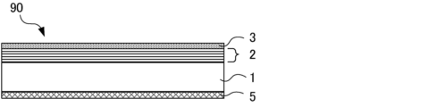
- FIG. 1 is a schematic cross-sectional view showing an example of a substrate 90 with a multilayer reflective film according to this embodiment.
- a substrate 90 with a multilayer reflective film of this embodiment includes a substrate 1 and a multilayer reflective film 2 provided on the substrate 1 .
- the multilayer reflective film 2 includes a multilayer film in which predetermined low refractive index layers and predetermined high refractive index layers are alternately laminated.
- a back surface conductive film 5 for an electrostatic chuck may be formed on the back surface of the substrate 1 (the surface opposite to the side on which the multilayer reflective film 2 is formed).
- the substrate 90 with a multilayer reflective film according to this embodiment will be specifically described.
- the substrate 1 preferably has a low coefficient of thermal expansion within the range of 0 ⁇ 5 ppb/° C. in order to prevent distortion of the transfer pattern due to heat during exposure to EUV light.
- a material having a low coefficient of thermal expansion within this range for example, SiO 2 —TiO 2 -based glass, multicomponent glass-ceramics, or the like can be used.
- the main surface (first main surface) of the substrate 1 on which the transfer pattern (absorber pattern 4a to be described later) is formed is preferably processed in order to increase the degree of flatness.
- the flatness is preferably 0.1 ⁇ m or less, more preferably 0.05 ⁇ m or less, and particularly preferably 0.05 ⁇ m or less in a 132 mm ⁇ 132 mm area of the main surface of the substrate 1 on which the transfer pattern is formed. It is preferably 0.03 ⁇ m or less.
- the second main surface (rear surface) opposite to the side on which the transfer pattern is formed is the surface fixed to the exposure device by an electrostatic chuck.
- the flatness is 0.1 ⁇ m or less, more preferably 0.05 ⁇ m or less, and particularly preferably 0.03 ⁇ m or less.
- the flatness is a value representing the warp (amount of deformation) of the surface indicated by TIR (Total Indicated Reading).
- TIR Total Indicated Reading
- the flatness (TIR) is measured by taking the surface of the substrate 1 as a reference and defining the plane determined by the method of least squares as the focal plane, and measuring the highest position of the surface of the substrate 1 above the focal plane and the substrate below the focal plane. It is the absolute value of the height difference with the lowest position of the surface of 1.
- the surface roughness of the main surface of the substrate 1 on which the transfer pattern is formed is preferably 0.1 nm or less in root-mean-square roughness (Rq).
- the surface roughness can be measured with an atomic force microscope.
- the substrate 1 preferably has high rigidity in order to prevent deformation of the thin film (multilayer reflective film 2, etc.) formed thereon due to film stress.
- those having a high Young's modulus of 65 GPa or more are preferred.
- low refractive index layers containing at least one selected from ruthenium (Ru) and rhodium (Rh) and high refractive index layers containing silicon (Si) are alternately laminated. Including multilayer film.
- the high refractive index layer is a layer containing silicon (Si).
- the high refractive index layer may contain Si alone or may contain a Si compound.
- the Si compound may contain Si and at least one element selected from the group consisting of B, C, N, O and H.
- the high refractive index layer is preferably made of silicon (Si). It should be noted that the phrase "the high refractive index layer is made of silicon (Si)" does not prevent impurities other than Si from being unavoidably mixed in the high refractive index layer. The same is true for other thin films and other elements.
- the low refractive index layer contains at least one selected from ruthenium (Ru) and rhodium (Rh).
- Ru ruthenium
- Rh rhodium
- the multilayer reflective film 2 includes a multilayer film in which low refractive index layers containing at least one selected from ruthenium (Ru) and rhodium (Rh) and high refractive index layers containing silicon (Si) are alternately laminated. As a result, the effective reflecting surface of the multilayer reflective film 2 can be made shallower than the conventional Mo/Si multilayer reflective film.
- Si in the high refractive index layer diffuses, which may cause a problem that the reflectance of the multilayer reflective film 2 to EUV light is lowered.
- the occurrence of this problem can be suppressed by including a predetermined additive element in addition to Ru and/or Rh in the low refractive index layer.
- the low refractive index layer of the substrate 90 with a multilayer reflective film of the present embodiment further contains an additive element having a work function in the range of more than 3.7 eV and less than 4.7 eV as a predetermined additive element.
- an additive element having a work function in the range of more than 3.7 eV and less than 4.7 eV as a predetermined additive element.
- the work function of Ru is 4.71 eV and the work function of Rh is 4.98 eV, so the work function of the additive element is lower than that of Ru. Therefore, by adding the additive element to the low refractive index layer, diffusion of the material (Si) of the high refractive index layer into the low refractive index layer can be suppressed.
- the high refractive index layer contains an element having a work function equal to or greater than that of Ru, there arises a problem that Si in the high refractive index layer diffuses into the low refractive index layer.
- the work function of Mg is 3.66 eV, the work function of the additive element is higher than that of Mg. If an element having a work function equal to or lower than that of Mg is added to the low refractive index layer, it becomes difficult to manufacture a pure metal target for deposition by sputtering. Therefore, the work function of the additive element must be within the range described above.
- the work function of an additive element means the work function of a metal composed of one kind of additive element, not an alloy.
- the additive element can also be selected based on the magnitude of the Fermi level of the metal. That is, the additive element contained in the low refractive index layer is a metal element having a Fermi level higher than that of Ru and lower than that of magnesium (Mg).
- Si which is the material of the high refractive index layer
- Si is known to have the property of diffusing easily into metal.
- the ease with which Si diffuses into metal depends on the work function of the metal. That is, when the work function of the metal of the low refractive index layer increases, Si diffuses easily into the metal (low refractive index layer). As a result, the reflectance of the EUV light by the multilayer reflective film 2 is lowered. A decrease in reflectance may occur particularly remarkably after the multilayer reflective film 2 is annealed. Conversely, when the work function of the metal becomes small, it becomes difficult for Si to diffuse into the metal (low refractive index layer). Therefore, the additive element contained in the low refractive index layer for forming the multilayer reflective film 2 in combination with the high refractive index layer containing Si is preferably a metal with a small work function.
- the additive element contained in the low refractive index layer for forming the multilayer reflective film 2 in combination with the high refractive index layer containing Si is preferably a metal with a small work function.
- the work function of Ru is smaller than 4.71 eV It can be understood that diffusion of Si into the low refractive index layer can be reduced in the case of the low refractive index layer containing an additive element having a work function. Also, it can be understood that the adhesion between the low refractive index layer and the high refractive index layer can be improved.
- the work function of Si is 4.61 eV (the difference between the vacuum level and the middle of the bandgap (Fermi level)).
- a low refractive index layer made of a material obtained by adding a predetermined additive element to Ru and/or Rh a high refractive index layer having a shallow effective reflection surface and containing Si can be changed from a high refractive index layer to a low refractive index layer. and the diffusion of Si atoms can be suppressed.
- the multilayer reflective film 2 of the substrate 90 with a multilayer reflective film can be prevented from lowering its reflectance for EUV light. Also, the adhesion between the low refractive index layer and the high refractive index layer of the multilayer reflective film 2 can be improved.
- Fig. 7 shows the relationship between the atomic number of the metal element and the work function.
- Elements inside the squares indicated by dashed lines in FIG. 7 are metal elements whose work functions are in the range of more than 3.7 eV and less than 4.7 eV.
- Table 2 shows a list of additive elements contained in the low refractive index layer of the multilayer reflective film 2 of the substrate 90 with the multilayer reflective film of this embodiment.
- Table 2 shows the work function, refractive index (n) and extinction coefficient (k) of each additive element.
- the additive element may be indicated as "X".
- the low refractive index layer is made of Ru and an additive element, the material of the low refractive index layer may be described as RuX.
- the low refractive index layer includes thallium (Tl), hafnium (Hf), titanium (Ti), zirconium (Zr), manganese (Mn), indium (In), gallium (Ga), and cadmium (Cd). , bismuth (Bi), tantalum (Ta), lead (Pb), silver (Ag), aluminum (Al), vanadium (V), niobium (Nb), tin (Sn), zinc (Zn), mercury (Hg) , chromium (Cr), iron (Fe), antimony (Sb), tungsten (W), molybdenum (Mo) and copper (Cu).
- the work functions of these additive elements are in the range of more than 3.7 eV and less than 4.7 eV. Therefore, the phenomenon that Si atoms diffuse from the high refractive index layer containing Si to the low refractive index layer can be suppressed, and the adhesion between the low refractive index layer and the high refractive index layer can be improved.
- the additive elements included in the anti-diffusion group A are additive elements having a work function of more than 3.7 eV and not more than 4.3 eV.
- the additive elements included in the diffusion prevention group B are additive elements having a work function higher than 4.3 eV and 4.5 eV or less.
- Additive elements included in diffusion-inhibiting group C are those with a work function higher than 4.5 eV and lower than 4.7 eV.
- the "diffusion prevention group" column in Table 2 shows the diffusion prevention group for each additive element.
- the additive elements belonging to diffusion prevention group A are Tl, Hf, Ti, Zr, Mn, In, Ga, Cd, Bi, Ta, Pb, Ag, Al, V, Nb and Sn.
- the additive elements belonging to the anti-diffusion group B are Zn, Hg, Cr and Fe.
- Additive elements belonging to diffusion prevention group C are Sb, W, Mo and Cu.
- the additive elements belonging to the anti-diffusion groups A, B and C can have a lower limit for the amount of addition of the low refractive index layer.
- the addition amount of the additive element of the diffusion prevention group A is preferably 1 atomic % or more, more preferably 3 atomic % or more.
- the addition amount of the additive element of the diffusion prevention group B is preferably 4 atomic % or more, more preferably 7 atomic % or more.
- the amount of the additive element added to the diffusion prevention group C is preferably 8 atomic % or more, more preferably 12 atomic % or more.
- the column of "lower limit (atomic %)" in Table 2 shows the diffusion prevention group of each additive element.
- the ratio of the content of the additive element of diffusion prevention group A to the content of the main material (Ru content, Rh content, or RuRh content) of the low refractive index layer is preferably 0.01 or more, more preferably 0.03 or more.
- the ratio of the content of the additive element of the diffusion prevention group B to the content of the main material of the low refractive index layer is preferably 0.04 or more, more preferably 0.08 or more.
- the ratio of the content of the additive element of the diffusion prevention group C to the content of the main material of the low refractive index layer is preferably 0.09 or more, more preferably 0.13 or more.
- the additive element is preferably an additive element belonging to anti-diffusion groups A and B, more preferably an additive element belonging to anti-diffusion group A. Further, a plurality of additive elements may be selected from diffusion prevention groups A, B and/or C.
- one high refractive index layer (Si) and a low refractive index layer 1 having a refractive index (n) of 0.88 or more and 0.96 or less and an extinction coefficient (k) of 0 or more and 0.08 or less A multilayer film was modeled by stacking 40 cycles of two layers stacked in this order as one cycle.
- the "reflectance for EUV light with a wavelength of 13.5 nm" means that the film thickness of the high refractive index layer is variable in the range of 0 nm or more and 6 nm or less, and the film thickness of the low refractive index layer is variable in the range of 0 nm or more and 6 nm or less. and the calculated maximum reflectance was used.
- the curve indicated by the dashed line shows the relationship between the refractive index (n) and the extinction coefficient (k).
- k 0.0021n -51.65 Expression (2) It is a curve showing that When the material of the low refractive index layer has a refractive index (n) and an extinction coefficient (k) on the dashed line of formula (2), the laminated structure of this low refractive index layer and the high refractive index layer of Si When the multilayer reflective film 2 is formed, the reflectance of the multilayer reflective film 2 for EUV light with a wavelength of 13.5 nm can be predicted to be 35% by simulation.
- one high refractive index layer (Si) and a low refractive index layer 1 having a refractive index (n) of 0.88 or more and 0.96 or less and an extinction coefficient (k) of 0 or more and 0.08 or less A multilayer film was modeled by stacking 40 cycles of two layers stacked in this order as one cycle.
- the "reflectance for EUV light with a wavelength of 13.5 nm" means that the film thickness of the high refractive index layer is variable in the range of 0 nm or more and 6 nm or less, and the film thickness of the low refractive index layer is variable in the range of 0 nm or more and 6 nm or less. and the calculated maximum reflectance was used.
- FIG. 8 shows the relationship between the refractive index (n) and the extinction coefficient (k) of each additive element.
- the reflectance for EUV light with a wavelength of 13.5 nm can be predicted from the values of the refractive index (n) and extinction coefficient (k) of the additive element.
- the multilayer reflective film 2 having a low refractive index layer of Mo and a high refractive index layer of Si from the values of the refractive index (n) and extinction coefficient (k) of Mo shown in FIG.
- the reflectance of the multilayer reflective film 2 for EUV light can be predicted.
- one cycle is composed of two layers, one high refractive index layer (Si) and one low refractive index layer, and the two layers are stacked in this order.
- the reflectance is the maximum reflectance predicted when the thickness of the high refractive index layer is variable in the range of 0 nm or more and 6 nm or less and the thickness of the low refractive index layer is variable in the range of 0 nm or more and 6 nm or less. is.
- FIG. 8 is a prediction when the number of layers of the multilayer reflective film 2 is 40, it can be said that the same tendency is observed even when the number of layers is less than 40, for example, about 35. .
- the additive elements can be divided into three optical property groups depending on the influence of the additive elements on the reflectance.
- the additive elements included in the optical property group a are additive elements with higher reflectance than the solid line (reflectance of 50%) of formula (1).
- the additive elements included in the optical property group b (shown as “Group b” in FIG. 8) have lower reflectance than the solid line (reflectance of 50%) in formula (1) and the dashed line in formula (2) ( It is an additive element with a higher reflectance than 35%).
- the additive elements included in the optical property group c (shown as “Group c” in FIG. 8) are additive elements with lower reflectance than the dashed line (reflectance of 35%) in formula (2).
- the column of "optical property group” in Table 2 shows the optical property group of each additive element.
- the amount of the additive element added to the low refractive index layer can have an upper limit. This is because the reflectance of the multilayer reflective film 2 decreases when the amount of the additive element added to the low refractive index layer is large.
- the amount of the additive element in the optical property group a is preferably 50 atomic % or less, more preferably 40 atomic % or less.
- the amount of the additive element in the optical property group b is preferably 30 atomic % or less, more preferably 20 atomic % or less.
- the amount of the additive element in the optical property group c is preferably 15 atomic % or less, more preferably 10 atomic % or less.
- the "upper limit (atomic %)" column in Table 2 shows the optical property group of each additive element.
- the ratio of the content of the additive element in the optical property group a to the content of the main material (Ru content, Rh content, or RuRh content) of the low refractive index layer (content of additive element/content of main material ) is preferably 0.56 or less, more preferably 0.44 or less.
- the ratio of the content of the additive element of the optical property group b to the content of the main material of the low refractive index layer is preferably 0.33 or less, more preferably 0.22 or less.
- the ratio of the content of the additive element of the optical property group c to the content of the main material of the low refractive index layer is preferably 0.17 or less, more preferably 0.11 or less.
- the additive elements belonging to optical property group a are zirconium (Zr), niobium (Nb), and molybdenum (Mo).
- the additive elements belonging to the optical property group b are thallium (Tl), titanium (Ti), manganese (Mn), indium (In), cadmium (Cd), tantalum (Ta), lead (Pb), silver (Ag), vanadium (V), mercury (Hg), chromium (Cr) and tungsten (W).
- the additive element is preferably an additive element belonging to optical property groups a and b, and more preferably an additive element belonging to optical property group a. Further, multiple additive elements may be selected from optical property groups a, b and/or c.
- the content of the main material is preferably more than 70 atomic % and less than 99 atomic %.
- the content of the main material is preferably more than 70 atomic % and less than 99 atomic %.
- Ga is the additive element
- the content of the main material is preferably more than 85 atomic % and less than 99 atomic %.
- Cd is the additive element
- the content of the main material is preferably more than 70 atomic % and less than 99 atomic %.
- Bi the additive element, the content of the main material is preferably more than 85 atomic % and less than 99 atomic %.
- the content of the main material is preferably more than 70 atomic % and less than 99 atomic %.
- Pb is the additive element
- the content of the main material is preferably more than 70 atomic % and less than 99 atomic %.
- Ag is the additive element
- the content of the main material is preferably more than 70 atomic % and less than 99 atomic %.
- Al is the additive element
- the content of the main material is preferably more than 85 atomic % and less than 99 atomic %.
- V is an additive element, the content of the main material is preferably more than 70 atomic % and less than 99 atomic %.
- the content of the main material is preferably more than 50 atomic % and less than 99 atomic %.
- Sn is the additive element
- the content of the main material is preferably more than 85 atomic % and less than 99 atomic %.
- Zn is the additive element
- the content of the main material is preferably more than 85 atomic % and less than 96 atomic %.
- Hg is the additive element
- the content of the main material is preferably more than 70 atomic % and less than 96 atomic %.
- Cr the additive element, the content of the main material is preferably more than 70 atomic % and less than 96 atomic %.
- the content of the main material is preferably more than 85 atomic % and less than 96 atomic %.
- Sb is the additive element
- the content of the main material is preferably more than 85 atomic % and less than 92 atomic %.
- W is the additive element
- the content of the main material is preferably more than 70 atomic % and less than 92 atomic %.
- Mo is the additive element
- the content of the main material is preferably more than 50 atomic % and less than 92 atomic %.
- Cu is the additive element, the content of the main material is preferably more than 85 atomic % and less than 92 atomic %.
- the appropriate blending of the alloying additive elements in the low refractive index layer is based on the appropriate content of each additive element and the amount of each element in the alloy. amount can be estimated.
- the low refractive index layer preferably does not contain elements other than the main materials Ru and Rh and the additive elements listed in Table 2. This is because when elements other than the main material and additive elements are contained, there is a high possibility that Si of the high refractive index layer will diffuse into the low refractive index layer. Therefore, the low refractive index layer preferably consists only of Ru and/or Rh and a predetermined additive element.
- the multilayer reflective film-coated substrate 90 of the present embodiment preferably has a laminated structure of less than 40 cycles when the laminated structure of the low refractive index layer and the high refractive index layer is defined as one cycle.
- the laminated structure of the multilayer reflective film 2 is more preferably 35 cycles or less, and even more preferably 30 cycles or less. Since the effective reflection surface of the multilayer reflective film 2 of this embodiment is shallow, an appropriate reflectance can be obtained with a smaller number of cycles than the conventional multilayer reflective film 2 . Therefore, the 3D effect can be suppressed by using the substrate 90 with a multilayer reflective film of this embodiment.
- the laminated structure preferably has 20 or more periods, more preferably 25 or more periods.
- the multilayer reflective film 2 When forming the multilayer reflective film 2, it is possible to first form a high refractive index layer on the surface of the substrate 1 and then form a low refractive index layer.
- the multilayer reflective film 2 has a laminated structure of a predetermined number of cycles on the substrate 1, with one cycle of a high refractive index layer and a low refractive index layer.
- the uppermost layer of the multilayer reflective film 2 is a low refractive index layer.
- the low refractive index layer constitutes the outermost surface of the multilayer reflective film 2, depending on the material constituting the low refractive index layer, it may be easily oxidized, and the reflectance of the reflective mask 200 is reduced. I have something to do.
- the multilayer reflective film 2 by further forming a high refractive index layer on the uppermost low refractive index layer.
- a Si layer made of Si may be formed on the uppermost low refractive index layer instead of the high refractive index layer.
- the multilayer reflective film 2 When forming the multilayer reflective film 2, it is possible to first form a low refractive index layer on the surface of the substrate 1 and then form a high and low refractive index layer.
- the multilayer reflective film 2 has a laminated structure with a predetermined number of cycles on the substrate 1, with each cycle having a low refractive index layer and a high refractive index layer.
- the uppermost layer is a high refractive index layer, so it may be left as it is.
- the top layer of the multilayer reflective film 2 is a high refractive index layer, it is preferable to form a protective film 3 described later on the multilayer reflective film 2 .
- the uppermost layer of the multilayer reflective film 2 can be the low refractive index layer.
- Ru has the function of protecting the multilayer reflective film 2 from dry etching and cleaning in the manufacturing process of the reflective mask 200, which will be described later.
- the uppermost low refractive index layer can also function as the protective film 3 .
- the structure of the multilayer reflective film 2 preferably includes a low refractive index layer containing Ru, and a high refractive index layer and a low refractive index layer containing Ru are laminated in this order from the substrate 1 side. Therefore, it is preferable to have a structure in which the uppermost layer is a low refractive index layer.
- the film thickness and composition of the uppermost low-refractive-index layer can be appropriately adjusted from the standpoint of dry etching resistance and cleaning resistance.
- the film thickness and composition of the uppermost low refractive index layer are preferably the same as those of the other low refractive index layers.
- the single reflectance of the multilayer reflective film 2 used in this embodiment is, for example, 65% or more.
- the upper limit of the reflectance of the multilayer reflective film 2 is, for example, 73%.
- the thickness and period of the layers included in the multilayer reflective film 2 can be selected so as to satisfy Bragg's law.
- the thickness of one period is preferably about 7 nm.
- the multilayer reflective film 2 can be formed by a known method.
- the multilayer reflective film 2 can be formed by, for example, an ion beam sputtering method, a magnetron sputtering method, a reactive sputtering method, or the like.
- the multilayer reflective film 2 is a RuNb/Si multilayer film in which Nb is an additive element of the low refractive index layer
- a RuNb film having a thickness of about 3 nm is formed on the substrate 1 by ion beam sputtering using a RuNb target. Form on top.
- a Si target using a Si target, a Si film having a thickness of about 4 nm is formed.
- the surface layer of the multilayer reflective film 2 opposite to the substrate 1 is a layer containing Si (Si film).
- the thickness of one period of the RuNb/Si film is preferably 7 nm.
- the multilayer reflective film-coated substrate 90 of the present embodiment preferably has a protective film 3 provided on the multilayer reflective film 2 .
- a protective film 3 is formed on the multilayer reflective film 2 or in contact with the surface of the multilayer reflective film 2 in order to protect the multilayer reflective film 2 from dry etching and cleaning in the manufacturing process of the reflective mask 200 to be described later. be able to.
- the protective film 3 also has a function of protecting the multilayer reflective film 2 during black defect correction of the transfer pattern (absorber pattern 4a) using an electron beam (EB).
- EB electron beam
- FIG. 2 shows the case where the protective film 3 is one layer.
- the protective film 3 can have a laminated structure of two layers.
- the protective film 3 has a laminated structure of three or more layers, the bottom layer and the top layer are made of, for example, a substance containing Ru, and a metal other than Ru or an alloy is placed between the bottom layer and the top layer. can be interposed.
- the protective film 3 is made of, for example, a material containing ruthenium as its main component.
- Materials containing ruthenium as a main component include Ru metal simple substance, Rh metal simple substance, Ru containing titanium (Ti), niobium (Nb), rhodium (Rh), molybdenum (Mo), zirconium (Zr), yttrium (Y), Ru alloys containing at least one metal selected from boron (B), lanthanum (La), cobalt (Co) and rhenium (Re), and materials containing nitrogen therein.
- the Ru content ratio of the Ru alloy used for the protective film 3 is 50 atomic % or more and less than 100 atomic %, preferably 80 atomic % or more and less than 100 atomic %, more preferably 95 atomic % or more and less than 100 atomic %.
- the protective film 3 has a mask cleaning resistance, an etching stopper function when the absorber film 4 is etched, and a function of preventing the multilayer reflective film 2 from changing with time while ensuring sufficient EUV light reflectance. It is possible to combine
- the protective film 3 preferably contains the same material as the low refractive index layer. Further, in the substrate 90 with a multilayer reflective film of the present embodiment, the protective film 3 contains at least one selected from ruthenium (Ru) and rhodium (Rh) and the same additive element (X) as the low refractive index layer. is more preferred.
- the low refractive index layer contains at least one selected from ruthenium (Ru) and rhodium (Rh), and the predetermined additive element X described above. Therefore, the protective film 3 also preferably contains the same material (RuX, RhX or RuRhX) as the low refractive index layer.
- the protection film 3 can be expected to function as a part of the multilayer reflective film 2 by including the same material as the low refractive index layer. Therefore, an improvement in the reflectance of the multilayer reflective film 2 can be expected.
- the protective film 3 can be formed more easily. More preferably, the protective film 3 is made of a material having the same element and the same composition ratio as the low refractive index layer.
- the film thickness of the protective film 3 is not particularly limited as long as it can function as the protective film 3 .
- the film thickness of the protective film 3 is preferably 1.0 nm to 8.0 nm, more preferably 1.5 nm to 6.0 nm.
- the film thickness of the protective film 3 is preferably the same film thickness as the low refractive index layer of the multilayer reflective film 2 .
- the protective film 3 is preferably formed in contact with the surface of the high refractive index layer of the multilayer reflective film 2 . As a result, the protective film 3 can function as part of the multilayer reflective film 2 .
- the uppermost layer of the multilayer reflective film 2 described above is a low refractive index layer
- this uppermost low refractive index layer can also serve as the protective film 3 .
- the low refractive index layer of this embodiment is a thin film made of ruthenium (Ru) and/or rhodium (Rh) and a predetermined additive element, it can function as the protective film 3 . Therefore, when manufacturing a reflective mask 200 (EUV mask) using the reflective mask blank 100 described later, damage to the surface of the multilayer reflective film 2 can be suppressed, so that the reflectance characteristics for EUV light can be improved. become good.
- a known film forming method can be adopted without particular limitation.
- Specific examples of the method for forming the protective film 3 include an ion beam sputtering method, a magnetron sputtering method, a reactive sputtering method, a chemical vapor deposition method (CVD), and a vacuum deposition method.
- the reflective mask blank 100 of this embodiment has an absorber film 4 on the multilayer reflective film 2 of the substrate 90 with the multilayer reflective film or on the protective film 3 formed on the multilayer reflective film 2 . Prepare.
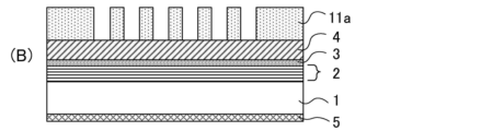
- FIG. 3 is a schematic cross-sectional view showing an example of the reflective mask blank 100 of this embodiment.
- a reflective mask blank 100 shown in FIG. 3 has an absorber film 4 for absorbing EUV light on the multilayer reflective film 2 of the substrate 90 with a multilayer reflective film shown in FIG. Note that the reflective mask blank 100 can further have other thin films such as the resist film 11 on the absorber film 4 .
- the top layer of the multilayer reflective film 2 is preferably a low refractive index layer containing RuX or RuRhX.
- FIG. 4 is a schematic cross-sectional view showing an example of the reflective mask blank 100 of this embodiment.
- a reflective mask blank 100 shown in FIG. 4 has an absorber film 4 for absorbing EUV light on the protective film 3 of the substrate 90 with a multilayer reflective film shown in FIG. Note that the reflective mask blank 100 can further have other thin films such as the resist film 11 on the absorber film 4 .
- FIG. 5 is a schematic cross-sectional view showing another example of the reflective mask blank 100 of this embodiment.
- the reflective mask blank 100 can have an etch mask film 6 over the absorber film 4 .
- the reflective mask blank 100 can further have another thin film such as a resist film 11 on the etching mask film 6 .
- the absorber film 4 can absorb EUV light.
- EUV masks can be manufactured.
- the reflective mask blank 100 of the present embodiment it has a shallow effective reflective surface, and it is possible to suppress the diffusion of material atoms between the low-refractive-index layer and the high-refractive-index layer.
- a reflective mask blank 100 having a multilayer reflective film 2 can be obtained.
- the basic function of the absorber film 4 is to absorb EUV light.
- the absorber film 4 may be an absorber film 4 intended to absorb EUV light, or an absorber film 4 having a phase shift function in consideration of the phase difference of EUV light.
- the absorber film 4 having a phase shift function absorbs EUV light and reflects part of the EUV light to shift the phase. That is, in the reflective mask 200 patterned with the absorber film 4 having a phase shift function, the portion where the absorber film 4 is formed absorbs the EUV light and reduces the light to a level that does not adversely affect the pattern transfer. to reflect some light.
- the EUV light is reflected by the multilayer reflective film 2 (via the protective film 3 if there is one). Therefore, a desired phase difference is generated between the reflected light from the absorber film 4 having a phase shift function and the reflected light from the field portion.
- the absorber film 4 having a phase shift function is preferably formed so that the phase difference between the reflected light from the absorber film 4 and the reflected light from the multilayer reflective film 2 is 170 degrees to 260 degrees.
- the image contrast of the projected optical image is improved by the interference of the light beams with the inverted phase difference at the pattern edge portion. As the image contrast is improved, the resolution is increased, and various latitudes related to exposure such as exposure amount latitude and focus latitude can be increased.
- the absorber film 4 may be a single-layer film, or may be a multilayer film composed of a plurality of films (for example, a lower-layer absorber film and an upper-layer absorber film).
- a single-layer film the number of steps in manufacturing mask blanks can be reduced, improving production efficiency.
- the optical constant and film thickness thereof can be appropriately set so that the upper absorber film serves as an anti-reflection film during mask pattern defect inspection using light. This improves the inspection sensitivity when inspecting mask pattern defects using light.
- a film added with oxygen (O), nitrogen (N), etc. which improves oxidation resistance, is used as the upper absorber film, the stability over time is improved.
- the absorber film 4 By making the absorber film 4 a multilayer film in this way, it is possible to add various functions to the absorber film 4 .
- the absorber film 4 has a phase shift function, it is possible to widen the range of adjustment on the optical surface by making it a multilayer film, so it becomes easy to obtain a desired reflectance.
- the material of the absorber film 4 has a function of absorbing EUV light and can be processed by etching (preferably by dry etching with chlorine (Cl)-based gas and/or fluorine (F)-based gas). and is not particularly limited as long as the material has a high etching selectivity with respect to the protective film 3 .
- Compounds may include oxygen (O), nitrogen (N), carbon (C) and/or boron (B) in the above metals or alloys.
- the absorber film 4 can be formed by magnetron sputtering such as DC sputtering and RF sputtering.
- the absorber film 4 made of a tantalum compound or the like can be formed by a reactive sputtering method using a target containing tantalum and boron and using argon gas to which oxygen or nitrogen is added.
- the crystalline state of the absorber film 4 is preferably amorphous or microcrystalline. If the surface of the absorber film 4 is not smooth or flat, the edge roughness of the absorber pattern 4a increases, and the dimensional accuracy of the pattern may deteriorate.
- the surface roughness of the absorber film 4 is preferably 0.5 nm or less, more preferably 0.4 nm or less, still more preferably 0.3 nm or less in terms of root mean square roughness (Rms).
- the reflective mask blank 100 of this embodiment can have an etching mask film 6 on the absorber film 4 .
- a material of the etching mask film 6 it is preferable to use a material having a high etching selection ratio of the absorber film 4 to the etching mask film 6 (etching rate of the absorber film 4/etching rate of the etching mask film 6).
- the etching selection ratio of the absorber film 4 to the etching mask film 6 is preferably 1.5 or more, more preferably 3 or more.
- the reflective mask blank 100 of this embodiment preferably has an etching mask film 6 on the absorber film 4 .
- chromium or a chromium compound examples include materials containing Cr and at least one element selected from N, O, C and H.
- the etching mask film 6 more preferably contains CrN, CrO, CrC, CrON, CrOC, CrCN, or CrOCN, and is a CrO-based film (CrO film, CrON film, CrOC film, or CrOCN film) containing chromium and oxygen. is more preferred.
- the material for the etching mask film 6 it is preferable to use tantalum or a tantalum compound.
- tantalum compounds include materials containing Ta and at least one element selected from N, O, B and H. More preferably, the etching mask film 6 contains TaN, TaO, TaON, TaBN, TaBO or TaBON.
- the film thickness of the etching mask film 6 is preferably 3 nm or more in order to accurately form a pattern on the absorber film 4 . Moreover, the film thickness of the etching mask film 6 is preferably 15 nm or less in order to reduce the film thickness of the resist film 11 .
- a back surface conductive film 5 for electrostatic chuck can be formed on the back surface of the substrate 10 (the surface opposite to the side on which the multilayer reflective film 2 is formed).
- the sheet resistance required for the back surface conductive film 5 for electrostatic chucking is usually 100 ⁇ /square ( ⁇ /square) or less.
- the back conductive film 5 can be formed, for example, by magnetron sputtering or ion beam sputtering using a metal such as chromium or tantalum, or an alloy target thereof.
- the material of the back conductive film 5 is preferably a material containing chromium (Cr) or tantalum (Ta).
- the material of the back conductive film 5 is preferably a Cr compound containing Cr and at least one selected from boron, nitrogen, oxygen, and carbon.
- Cr compounds include CrN, CrON, CrCN, CrCON, CrBN, CrBON, CrBCN and CrBOCN.
- the material of the back conductive film 5 is preferably Ta (tantalum), an alloy containing Ta, or a Ta compound containing at least one of boron, nitrogen, oxygen, and carbon in any of these.
- Ta compounds include TaB, TaN, TaO, TaON, TaCON, TaBN, TaBO, TaBON, TaBCON, TaHf, TaHfO, TaHfN, TaHfON, TaHfCON, TaSi, TaSiO, TaSiN, TaSiON, and TaSiCON. can.
- the film thickness of the back surface conductive film 5 is not particularly limited as long as it functions as a film for an electrostatic chuck.
- the thickness of the back conductive film 5 is, for example, 10 nm to 200 nm.
- the reflective mask 200 of this embodiment includes an absorber pattern 4a obtained by patterning the absorber film 4 of the reflective mask blank 100 described above.
- FIG. 6A to 6D are schematic diagrams showing an example of a method for manufacturing the reflective mask 200.
- FIG. The reflective mask blank 100 of the present embodiment described above can be used to manufacture the reflective mask 200 of the present embodiment.
- An example of a method for manufacturing the reflective mask 200 will be described below.
- a substrate 1, a multilayer reflective film 2 formed on the substrate 1, a protective film 3 formed on the multilayer reflective film 2, and an absorber film 4 formed on the protective film 3 are provided.
- a reflective mask blank 100 is prepared.
- a resist film 11 is formed on the absorber film 4 to obtain a reflective mask blank 100 with the resist film 11 (FIG. 6A).
- a pattern is drawn on the resist film 11 by an electron beam drawing apparatus, and a resist pattern 11a is formed by developing and rinsing (FIG. 6B).
- etching gas for the absorber film 4 for example, a fluorine-based gas and/or a chlorine-based gas can be used.
- Fluorinated gases include CF4 , CHF3 , C2F6, C3F6, C4F6 , C4F8 , CH2F2 , CH3F , C3F8 , SF6 , and F2 . etc. can be used.
- Cl 2 , SiCl 4 , CHCl 3 , CCl 4 , BCl 3 and the like can be used as the chlorine-based gas.
- a mixed gas containing a fluorine-based gas and/or a chlorine-based gas and O 2 in a predetermined ratio can be used.
- These etching gases can optionally further contain inert gases such as He and/or Ar.
- the resist pattern 11a is removed with a resist remover.
- the reflective mask 200 of the present embodiment can be obtained through a wet cleaning process using an acidic or alkaline aqueous solution (FIG. 6D).
- a pattern (etching mask pattern) is formed on the etching mask film 6 using the resist pattern 11a as a mask. After that, a step of forming a pattern on the absorber film 4 using the etching mask pattern as a mask is added.
- the reflective mask 200 thus obtained has a structure in which a multilayer reflective film 2, a protective film 3, and an absorber pattern 4a are laminated on a substrate 1.
- the exposed area of the multilayer reflective film 2 (including the protective film 3) has the function of reflecting EUV light.
- the reflective mask 200 of this embodiment has a shallow effective reflective surface, and is a multilayer reflective film capable of suppressing the diffusion of material atoms between the low-refractive-index layer and the high-refractive-index layer. have Therefore, by using the reflective mask 200 of this embodiment, it is possible to transfer a finer pattern to the transfer target.
- the manufacturing method of the semiconductor device of this embodiment has a step of performing a lithography process using an exposure apparatus using the above-described reflective mask 200 to form a transfer pattern on a transfer target.
- a transfer pattern can be formed on a semiconductor substrate (transfer target) by lithography using the reflective mask 200 of this embodiment. This transfer pattern has a shape obtained by transferring the pattern of the reflective mask 200 .
- a semiconductor device can be manufactured by forming a transfer pattern on a semiconductor substrate using the reflective mask 200 .
- the multilayer reflective film 2 has a shallow effective reflective surface and can suppress the diffusion of material atoms between the low refractive index layer and the high refractive index layer.
- a semiconductor device can be manufactured using the reflective mask 200 . Therefore, by using the reflective mask 200 of this embodiment, the density and accuracy of the semiconductor device can be increased.
- FIG. 9 shows a schematic configuration of an EUV exposure apparatus 50, which is an apparatus for transferring a transfer pattern onto a resist film formed on a semiconductor substrate 60.
- an EUV light generator 51 an irradiation optical system 56, a reticle stage 58, a projection optical system 57, and a wafer stage 59 are precisely arranged along the optical path axis of EUV light.
- the container of the EUV exposure apparatus 50 is filled with hydrogen gas.
- the EUV light generation section 51 has a laser light source 52 , a tin droplet generation section 53 , a capture section 54 and a collector 55 .
- the tin droplets emitted from the tin droplet generator 53 are irradiated with a high-power carbon dioxide laser from the laser light source 52, the tin droplets are plasmatized to generate EUV light.
- the generated EUV light is collected by a collector 55 and made incident on a reflective mask 200 set on a reticle stage 58 via an irradiation optical system 56 .
- the EUV light generator 51 generates EUV light with a wavelength of 13.53 nm, for example.
- the EUV light reflected by the reflective mask 200 is normally reduced to about 1/4 of the pattern image light by the projection optical system 57 and projected onto the semiconductor substrate 60 (transferred substrate). Thereby, a given circuit pattern is transferred to the resist film on the semiconductor substrate 60 .
- a resist pattern can be formed on the semiconductor substrate 60 by developing the exposed resist film. By etching the semiconductor substrate 60 using the resist pattern as a mask, an integrated circuit pattern can be formed on the semiconductor substrate.
- a semiconductor device is manufactured through these processes and other necessary processes.
- a substrate 1 of 6025 size (approximately 152 mm ⁇ 152 mm ⁇ 6.35 mm) having polished first and second main surfaces was prepared.
- This substrate 1 is made of low thermal expansion glass (SiO 2 —TiO 2 based glass).
- the main surface of the substrate 1 was polished through a rough polishing process, a fine polishing process, a local polishing process, and a touch polishing process.
- a multilayer reflective film 2 composed of a Si high refractive index layer and a predetermined low refractive index layer was formed.
- Table 1 shows the materials and compositions of the low refractive index layers (RuX or RuRhX, where X is an additive element) of Examples 1 to 10.
- the material of the high refractive index layer in Examples 1-10 is Si.
- Table 1 shows the work function of the additive element (X) and the content (atomic %) of the additive element (X) in the low refractive index layer.
- the multilayer reflective film 2 was formed by ion beam sputtering using a Si target and a RuX target or RuRhX target (where X is an additive element) using Kr gas.
- a Si target is used to form a high refractive index layer of Si with a thickness of 4.2 nm so as to be in contact with the main surface of the substrate 1, followed by a RuX target or RuRhX target (where X is an additive element). was used to form a RuX or RuRhX low refractive index layer with a film thickness of 2.8 nm.
- the multilayer reflective film 2 was formed by laminating 35 periods (pairs) on the main surface of the substrate 1, with one period consisting of lamination of one high refractive index layer and one low refractive index layer.
- a RuRhNb film was formed as a protective film 3 on the multilayer reflective film 2 of Examples 1-10.
- the protective film 3 was formed with a thickness of 3.5 nm by magnetron sputtering in an Ar gas atmosphere using a RuRhNb target.
- the substrates 90 with multilayer reflective films of Examples 1 to 10 were manufactured.
- a substrate 90 with a multilayer reflective film was manufactured in the same manner as in Examples 1 to 10, except that the material of the low refractive index layer was Ru (Comparative Example 1) or RuRh (Comparative Example 2). Accordingly, the low refractive index layers of Comparative Examples 1 and 2 do not contain the additive element (X).
- a Ru target was used, and when forming the low refractive index layer of Comparative Example 2, a RuRh target was used.
- Table 1 shows the composition ratio (atomic %) of the low refractive index layers of Comparative Examples 1 and 2.
- the reflectance (R1, unit %) for EUV light (wavelength 13.5 nm) of the substrates 90 with multilayer reflective films of Examples and Comparative Examples was measured.
- the substrate 90 with the multilayer reflective film was heat-treated by heating at 200° C. for 10 minutes in an air atmosphere.
- the reflectance (R2, unit %) of the substrate 90 with the multilayer reflective film to EUV light was measured.
- the EUV due to the heat treatment of the substrate 90 with the multilayer reflective film A change in reflectance was obtained.
- Table 1 shows changes in EUV reflectance due to heat treatment.
- Example 7 the change in reflectance for EUV light before and after heat treatment at 200° C. for 10 minutes was 9.4% (Example 7) or less. was. Since the material of the low refractive index layer of the multilayer reflective film 2 of Examples 1 to 10 was RuX or RuRhX containing a predetermined additive element (X), diffusion of Si from the high refractive index layer to the low refractive index layer did not occur. Suppressed. Therefore, it is presumed that the change in reflectance was small before and after the heat treatment. In particular, the reflectance change of Example 1, in which the material of the low refractive index layer is RuNb, was as small as 6.9%.
- the reflectance of the substrates 90 with the multilayer reflective film with respect to EUV light changed significantly before and after the heat treatment at 200° C. for 10 minutes.
- Si diffused from the high refractive index layer to the low refractive index layer to form metal silicide (RuSi or RuRhSi) in the high refractive index layer, resulting in a large change in reflectance. It is speculated that
- the A reflective mask blank 100 was manufactured.
- a back conductive film 5 made of a CrN film was formed on the second main surface (back surface) of substrate 1 of substrate 90 with a multilayer reflective film by magnetron sputtering (reactive sputtering) under the following conditions.
- Conditions for forming the back conductive film 5 Cr target, mixed gas atmosphere of Ar and N2 (Ar: 90%, N: 10%), film thickness 20 nm.
- the reflective mask blanks 100 of Examples 1 to 10 were manufactured.
- Reflective mask 200 Next, using the reflective mask blanks 100 of Examples 1 to 10, reflective masks 200 were manufactured. The fabrication of the reflective mask 200 will be described with reference to FIGS. 6A through 6D.
- a resist film 11 was formed on the absorber film 4 of the reflective mask blank 100 .
- a desired pattern such as a circuit pattern was drawn (exposed) on the resist film 11, developed, and rinsed to form a predetermined resist pattern 11a (FIG. 6B).
- the absorber film 4 (TaBN film) was dry-etched using Cl 2 gas to form an absorber pattern 4a (FIG. 6C). After that, the resist pattern 11a was removed (FIG. 6D).
- the reflective masks 200 of Examples 1 to 10 were set on an EUV scanner, and EUV exposure was performed on a wafer in which a film to be processed and a resist film were formed on a semiconductor substrate 60 as a transfer target. Then, by developing the exposed resist film, a resist pattern was formed on the semiconductor substrate 56 on which the film to be processed was formed.
- the reflective mask 200 of Examples 1 to 10 has a shallow effective reflective surface, and is a multi-layer mask that can suppress the diffusion of material atoms between the low-refractive-index layer and the high-refractive-index layer. Since the reflective film 2 was provided, a fine and highly accurate transfer pattern (resist pattern) could be formed on the semiconductor substrate 60 (substrate to be transferred).
- This resist pattern is transferred to the film to be processed by etching, and various processes such as the formation of insulating films and conductive films, the introduction of dopants, and annealing are performed to manufacture semiconductor devices with desired characteristics at a high yield. We were able to.
Landscapes
- Physics & Mathematics (AREA)
- General Physics & Mathematics (AREA)
- Spectroscopy & Molecular Physics (AREA)
- Engineering & Computer Science (AREA)
- General Engineering & Computer Science (AREA)
- High Energy & Nuclear Physics (AREA)
- Exposure Of Semiconductors, Excluding Electron Or Ion Beam Exposure (AREA)
- Preparing Plates And Mask In Photomechanical Process (AREA)
- Optical Elements Other Than Lenses (AREA)
Priority Applications (3)
| Application Number | Priority Date | Filing Date | Title |
|---|---|---|---|
| KR1020247003753A KR20240055724A (ko) | 2021-09-07 | 2022-09-02 | 다층 반사막 구비 기판, 반사형 마스크 블랭크, 반사형 마스크 및 반도체 장치의 제조 방법 |
| US18/682,747 US20250370324A1 (en) | 2021-09-07 | 2022-09-02 | Multilayer reflective film-attached substrate, reflective mask blank, reflective mask, and method for manufacturing semiconductor device |
| JP2023546920A JPWO2023037980A1 (https=) | 2021-09-07 | 2022-09-02 |
Applications Claiming Priority (2)
| Application Number | Priority Date | Filing Date | Title |
|---|---|---|---|
| JP2021145749 | 2021-09-07 | ||
| JP2021-145749 | 2021-09-07 |
Publications (1)
| Publication Number | Publication Date |
|---|---|
| WO2023037980A1 true WO2023037980A1 (ja) | 2023-03-16 |
Family
ID=85507564
Family Applications (1)
| Application Number | Title | Priority Date | Filing Date |
|---|---|---|---|
| PCT/JP2022/033127 Ceased WO2023037980A1 (ja) | 2021-09-07 | 2022-09-02 | 多層反射膜付き基板、反射型マスクブランク、反射型マスク、及び半導体装置の製造方法 |
Country Status (5)
| Country | Link |
|---|---|
| US (1) | US20250370324A1 (https=) |
| JP (1) | JPWO2023037980A1 (https=) |
| KR (1) | KR20240055724A (https=) |
| TW (1) | TW202321815A (https=) |
| WO (1) | WO2023037980A1 (https=) |
Cited By (2)
| Publication number | Priority date | Publication date | Assignee | Title |
|---|---|---|---|---|
| EP4509921A1 (en) * | 2023-08-16 | 2025-02-19 | Shin-Etsu Chemical Co., Ltd. | Reflective mask blank and manufacturing method of reflective mask |
| WO2025142825A1 (ja) * | 2023-12-27 | 2025-07-03 | Hoya株式会社 | 反射型マスクブランク、反射型マスク、及び半導体装置の製造方法 |
Citations (4)
| Publication number | Priority date | Publication date | Assignee | Title |
|---|---|---|---|---|
| JP2006093454A (ja) * | 2004-09-24 | 2006-04-06 | Hoya Corp | 反射型マスクブランク、反射型マスク及び多層膜反射鏡 |
| JP2006173446A (ja) * | 2004-12-17 | 2006-06-29 | Nikon Corp | 極端紫外線用の光学素子及びこれを用いた投影露光装置 |
| JP2014056960A (ja) * | 2012-09-13 | 2014-03-27 | Asahi Glass Co Ltd | Euvリソグラフィ用反射型マスクブランクおよびその製造方法、ならびに該マスクブランク用の反射層付基板およびその製造方法 |
| JP2021039271A (ja) * | 2019-09-04 | 2021-03-11 | Hoya株式会社 | 多層反射膜付き基板、反射型マスクブランク及び反射型マスク、並びに半導体装置の製造方法 |
Family Cites Families (4)
| Publication number | Priority date | Publication date | Assignee | Title |
|---|---|---|---|---|
| JP2723955B2 (ja) | 1989-03-16 | 1998-03-09 | キヤノン株式会社 | 軟x線・真空紫外線用多層膜反射鏡 |
| JP3097778B2 (ja) | 1992-01-23 | 2000-10-10 | 日本電信電話株式会社 | 多層膜分光反射鏡 |
| JPH09230098A (ja) | 1996-02-21 | 1997-09-05 | Nippon Telegr & Teleph Corp <Ntt> | 多層膜x線反射鏡 |
| KR20210089406A (ko) | 2020-01-08 | 2021-07-16 | 주식회사 에스앤에스텍 | 극자외선용 반사형 블랭크 마스크 및 포토마스크 |
-
2022
- 2022-09-02 JP JP2023546920A patent/JPWO2023037980A1/ja active Pending
- 2022-09-02 WO PCT/JP2022/033127 patent/WO2023037980A1/ja not_active Ceased
- 2022-09-02 KR KR1020247003753A patent/KR20240055724A/ko active Pending
- 2022-09-02 US US18/682,747 patent/US20250370324A1/en active Pending
- 2022-09-05 TW TW111133520A patent/TW202321815A/zh unknown
Patent Citations (4)
| Publication number | Priority date | Publication date | Assignee | Title |
|---|---|---|---|---|
| JP2006093454A (ja) * | 2004-09-24 | 2006-04-06 | Hoya Corp | 反射型マスクブランク、反射型マスク及び多層膜反射鏡 |
| JP2006173446A (ja) * | 2004-12-17 | 2006-06-29 | Nikon Corp | 極端紫外線用の光学素子及びこれを用いた投影露光装置 |
| JP2014056960A (ja) * | 2012-09-13 | 2014-03-27 | Asahi Glass Co Ltd | Euvリソグラフィ用反射型マスクブランクおよびその製造方法、ならびに該マスクブランク用の反射層付基板およびその製造方法 |
| JP2021039271A (ja) * | 2019-09-04 | 2021-03-11 | Hoya株式会社 | 多層反射膜付き基板、反射型マスクブランク及び反射型マスク、並びに半導体装置の製造方法 |
Cited By (2)
| Publication number | Priority date | Publication date | Assignee | Title |
|---|---|---|---|---|
| EP4509921A1 (en) * | 2023-08-16 | 2025-02-19 | Shin-Etsu Chemical Co., Ltd. | Reflective mask blank and manufacturing method of reflective mask |
| WO2025142825A1 (ja) * | 2023-12-27 | 2025-07-03 | Hoya株式会社 | 反射型マスクブランク、反射型マスク、及び半導体装置の製造方法 |
Also Published As
| Publication number | Publication date |
|---|---|
| JPWO2023037980A1 (https=) | 2023-03-16 |
| US20250370324A1 (en) | 2025-12-04 |
| KR20240055724A (ko) | 2024-04-29 |
| TW202321815A (zh) | 2023-06-01 |
Similar Documents
| Publication | Publication Date | Title |
|---|---|---|
| TWI811369B (zh) | 反射型光罩基底、反射型光罩、以及反射型光罩及半導體裝置之製造方法 | |
| JP2025113408A (ja) | 反射型マスクブランク、反射型マスク及びその製造方法、並びに半導体装置の製造方法 | |
| JP7193344B2 (ja) | 反射型マスクブランク、反射型マスクの製造方法、及び半導体装置の製造方法 | |
| US20230418148A1 (en) | Multilayer reflective film-equipped substrate, reflective mask blank, reflective mask, and method for producing semiconductor device | |
| JP7263908B2 (ja) | 反射型マスクブランク、反射型マスク及び反射型マスクブランクの製造方法 | |
| JP7679357B2 (ja) | 多層反射膜付き基板、反射型マスクブランク、反射型マスク、及び半導体装置の製造方法 | |
| JP7688757B2 (ja) | 多層反射膜付き基板、反射型マスクブランク、反射型マスク、及び半導体装置の製造方法 | |
| US20240027891A1 (en) | Reflective mask blank, reflective mask, and method for manufacturing semiconductor device | |
| US20240377719A1 (en) | Substrate with multilayer reflective film reflective mask blank, reflective mask, and method for manufacturing semiconductor device | |
| WO2023037980A1 (ja) | 多層反射膜付き基板、反射型マスクブランク、反射型マスク、及び半導体装置の製造方法 | |
| US20240411220A1 (en) | Multilayer reflective film-attached substrate, reflective mask blank, reflective mask, and method for producing semiconductor device | |
| WO2022210334A1 (ja) | 反射型マスクブランク、反射型マスク、反射型マスクの製造方法、及び半導体装置の製造方法 | |
| JP7837943B2 (ja) | 多層反射膜付き基板、反射型マスクブランク、反射型マスク、及び半導体装置の製造方法 | |
| WO2024085026A1 (ja) | 反射型マスクブランク及び反射型マスク、並びに反射型マスク及び半導体装置の製造方法 | |
| KR102961090B1 (ko) | 다층 반사막 부착 기판, 반사형 마스크 블랭크 및 반사형 마스크, 그리고 반도체 장치의 제조 방법 | |
| TW202544546A (zh) | 附多層反射膜基板、反射型遮罩基底及反射型遮罩、以及半導體裝置之製造方法 | |
| WO2025205962A1 (ja) | 多層反射膜付き基板、反射型マスクブランク、反射型マスク、及び半導体装置の製造方法 | |
| WO2025023299A1 (ja) | 多層反射膜付き基板、反射型マスクブランク、反射型マスク、及び半導体装置の製造方法 | |
| TW202414072A (zh) | 附多層反射膜之基板、反射型光罩基底、反射型光罩以及半導體裝置之製造方法 | |
| WO2025142825A1 (ja) | 反射型マスクブランク、反射型マスク、及び半導体装置の製造方法 |
Legal Events
| Date | Code | Title | Description |
|---|---|---|---|
| 121 | Ep: the epo has been informed by wipo that ep was designated in this application |
Ref document number: 22867302 Country of ref document: EP Kind code of ref document: A1 |
|
| WWE | Wipo information: entry into national phase |
Ref document number: 2023546920 Country of ref document: JP |
|
| NENP | Non-entry into the national phase |
Ref country code: DE |
|
| 122 | Ep: pct application non-entry in european phase |
Ref document number: 22867302 Country of ref document: EP Kind code of ref document: A1 |