WO2023032612A1 - 信号伝達装置および絶縁チップ - Google Patents
信号伝達装置および絶縁チップ Download PDFInfo
- Publication number
- WO2023032612A1 WO2023032612A1 PCT/JP2022/030341 JP2022030341W WO2023032612A1 WO 2023032612 A1 WO2023032612 A1 WO 2023032612A1 JP 2022030341 W JP2022030341 W JP 2022030341W WO 2023032612 A1 WO2023032612 A1 WO 2023032612A1
- Authority
- WO
- WIPO (PCT)
- Prior art keywords
- insulating layer
- coil
- chip
- thickness
- substrate
- Prior art date
- Legal status (The legal status is an assumption and is not a legal conclusion. Google has not performed a legal analysis and makes no representation as to the accuracy of the status listed.)
- Ceased
Links
Images










Classifications
-
- H—ELECTRICITY
- H10—SEMICONDUCTOR DEVICES; ELECTRIC SOLID-STATE DEVICES NOT OTHERWISE PROVIDED FOR
- H10W—GENERIC PACKAGES, INTERCONNECTIONS, CONNECTORS OR OTHER CONSTRUCTIONAL DETAILS OF DEVICES COVERED BY CLASS H10
- H10W90/00—Package configurations
-
- H—ELECTRICITY
- H01—ELECTRIC ELEMENTS
- H01F—MAGNETS; INDUCTANCES; TRANSFORMERS; SELECTION OF MATERIALS FOR THEIR MAGNETIC PROPERTIES
- H01F19/00—Fixed transformers or mutual inductances of the signal type
- H01F19/04—Transformers or mutual inductances suitable for handling frequencies considerably beyond the audio range
-
- H—ELECTRICITY
- H03—ELECTRONIC CIRCUITRY
- H03K—PULSE TECHNIQUE
- H03K17/00—Electronic switching or gating, i.e. not by contact-making and –breaking
- H03K17/51—Electronic switching or gating, i.e. not by contact-making and –breaking characterised by the components used
- H03K17/56—Electronic switching or gating, i.e. not by contact-making and –breaking characterised by the components used by the use, as active elements, of semiconductor devices
- H03K17/687—Electronic switching or gating, i.e. not by contact-making and –breaking characterised by the components used by the use, as active elements, of semiconductor devices the devices being field-effect transistors
- H03K17/689—Electronic switching or gating, i.e. not by contact-making and –breaking characterised by the components used by the use, as active elements, of semiconductor devices the devices being field-effect transistors with galvanic isolation between the control circuit and the output circuit
- H03K17/691—Electronic switching or gating, i.e. not by contact-making and –breaking characterised by the components used by the use, as active elements, of semiconductor devices the devices being field-effect transistors with galvanic isolation between the control circuit and the output circuit using transformer coupling
-
- H—ELECTRICITY
- H10—SEMICONDUCTOR DEVICES; ELECTRIC SOLID-STATE DEVICES NOT OTHERWISE PROVIDED FOR
- H10D—INORGANIC ELECTRIC SEMICONDUCTOR DEVICES
- H10D84/00—Integrated devices formed in or on semiconductor substrates that comprise only semiconducting layers, e.g. on Si wafers or on GaAs-on-Si wafers
-
- H—ELECTRICITY
- H10—SEMICONDUCTOR DEVICES; ELECTRIC SOLID-STATE DEVICES NOT OTHERWISE PROVIDED FOR
- H10W—GENERIC PACKAGES, INTERCONNECTIONS, CONNECTORS OR OTHER CONSTRUCTIONAL DETAILS OF DEVICES COVERED BY CLASS H10
- H10W72/00—Interconnections or connectors in packages
- H10W72/90—Bond pads, in general
-
- H—ELECTRICITY
- H10—SEMICONDUCTOR DEVICES; ELECTRIC SOLID-STATE DEVICES NOT OTHERWISE PROVIDED FOR
- H10D—INORGANIC ELECTRIC SEMICONDUCTOR DEVICES
- H10D86/00—Integrated devices formed in or on insulating or conducting substrates, e.g. formed in silicon-on-insulator [SOI] substrates or on stainless steel or glass substrates
- H10D86/80—Integrated devices formed in or on insulating or conducting substrates, e.g. formed in silicon-on-insulator [SOI] substrates or on stainless steel or glass substrates characterised by multiple passive components, e.g. resistors, capacitors or inductors
- H10D86/85—Integrated devices formed in or on insulating or conducting substrates, e.g. formed in silicon-on-insulator [SOI] substrates or on stainless steel or glass substrates characterised by multiple passive components, e.g. resistors, capacitors or inductors characterised by only passive components
-
- H—ELECTRICITY
- H10—SEMICONDUCTOR DEVICES; ELECTRIC SOLID-STATE DEVICES NOT OTHERWISE PROVIDED FOR
- H10W—GENERIC PACKAGES, INTERCONNECTIONS, CONNECTORS OR OTHER CONSTRUCTIONAL DETAILS OF DEVICES COVERED BY CLASS H10
- H10W72/00—Interconnections or connectors in packages
- H10W72/30—Die-attach connectors
- H10W72/351—Materials of die-attach connectors
- H10W72/352—Materials of die-attach connectors comprising metals or metalloids, e.g. solders
-
- H—ELECTRICITY
- H10—SEMICONDUCTOR DEVICES; ELECTRIC SOLID-STATE DEVICES NOT OTHERWISE PROVIDED FOR
- H10W—GENERIC PACKAGES, INTERCONNECTIONS, CONNECTORS OR OTHER CONSTRUCTIONAL DETAILS OF DEVICES COVERED BY CLASS H10
- H10W72/00—Interconnections or connectors in packages
- H10W72/30—Die-attach connectors
- H10W72/351—Materials of die-attach connectors
- H10W72/353—Materials of die-attach connectors not comprising solid metals or solid metalloids, e.g. ceramics
- H10W72/354—Materials of die-attach connectors not comprising solid metals or solid metalloids, e.g. ceramics comprising polymers
-
- H—ELECTRICITY
- H10—SEMICONDUCTOR DEVICES; ELECTRIC SOLID-STATE DEVICES NOT OTHERWISE PROVIDED FOR
- H10W—GENERIC PACKAGES, INTERCONNECTIONS, CONNECTORS OR OTHER CONSTRUCTIONAL DETAILS OF DEVICES COVERED BY CLASS H10
- H10W72/00—Interconnections or connectors in packages
- H10W72/50—Bond wires
-
- H—ELECTRICITY
- H10—SEMICONDUCTOR DEVICES; ELECTRIC SOLID-STATE DEVICES NOT OTHERWISE PROVIDED FOR
- H10W—GENERIC PACKAGES, INTERCONNECTIONS, CONNECTORS OR OTHER CONSTRUCTIONAL DETAILS OF DEVICES COVERED BY CLASS H10
- H10W72/00—Interconnections or connectors in packages
- H10W72/50—Bond wires
- H10W72/541—Dispositions of bond wires
- H10W72/5445—Dispositions of bond wires being orthogonal to a side surface of the chip, e.g. parallel arrangements
-
- H—ELECTRICITY
- H10—SEMICONDUCTOR DEVICES; ELECTRIC SOLID-STATE DEVICES NOT OTHERWISE PROVIDED FOR
- H10W—GENERIC PACKAGES, INTERCONNECTIONS, CONNECTORS OR OTHER CONSTRUCTIONAL DETAILS OF DEVICES COVERED BY CLASS H10
- H10W72/00—Interconnections or connectors in packages
- H10W72/50—Bond wires
- H10W72/551—Materials of bond wires
- H10W72/552—Materials of bond wires comprising metals or metalloids, e.g. silver
- H10W72/5522—Materials of bond wires comprising metals or metalloids, e.g. silver comprising gold [Au]
-
- H—ELECTRICITY
- H10—SEMICONDUCTOR DEVICES; ELECTRIC SOLID-STATE DEVICES NOT OTHERWISE PROVIDED FOR
- H10W—GENERIC PACKAGES, INTERCONNECTIONS, CONNECTORS OR OTHER CONSTRUCTIONAL DETAILS OF DEVICES COVERED BY CLASS H10
- H10W72/00—Interconnections or connectors in packages
- H10W72/50—Bond wires
- H10W72/551—Materials of bond wires
- H10W72/552—Materials of bond wires comprising metals or metalloids, e.g. silver
- H10W72/5524—Materials of bond wires comprising metals or metalloids, e.g. silver comprising aluminium [Al]
-
- H—ELECTRICITY
- H10—SEMICONDUCTOR DEVICES; ELECTRIC SOLID-STATE DEVICES NOT OTHERWISE PROVIDED FOR
- H10W—GENERIC PACKAGES, INTERCONNECTIONS, CONNECTORS OR OTHER CONSTRUCTIONAL DETAILS OF DEVICES COVERED BY CLASS H10
- H10W72/00—Interconnections or connectors in packages
- H10W72/50—Bond wires
- H10W72/551—Materials of bond wires
- H10W72/552—Materials of bond wires comprising metals or metalloids, e.g. silver
- H10W72/5525—Materials of bond wires comprising metals or metalloids, e.g. silver comprising copper [Cu]
-
- H—ELECTRICITY
- H10—SEMICONDUCTOR DEVICES; ELECTRIC SOLID-STATE DEVICES NOT OTHERWISE PROVIDED FOR
- H10W—GENERIC PACKAGES, INTERCONNECTIONS, CONNECTORS OR OTHER CONSTRUCTIONAL DETAILS OF DEVICES COVERED BY CLASS H10
- H10W72/00—Interconnections or connectors in packages
- H10W72/851—Dispositions of multiple connectors or interconnections
-
- H—ELECTRICITY
- H10—SEMICONDUCTOR DEVICES; ELECTRIC SOLID-STATE DEVICES NOT OTHERWISE PROVIDED FOR
- H10W—GENERIC PACKAGES, INTERCONNECTIONS, CONNECTORS OR OTHER CONSTRUCTIONAL DETAILS OF DEVICES COVERED BY CLASS H10
- H10W72/00—Interconnections or connectors in packages
- H10W72/851—Dispositions of multiple connectors or interconnections
- H10W72/874—On different surfaces
- H10W72/884—Die-attach connectors and bond wires
-
- H—ELECTRICITY
- H10—SEMICONDUCTOR DEVICES; ELECTRIC SOLID-STATE DEVICES NOT OTHERWISE PROVIDED FOR
- H10W—GENERIC PACKAGES, INTERCONNECTIONS, CONNECTORS OR OTHER CONSTRUCTIONAL DETAILS OF DEVICES COVERED BY CLASS H10
- H10W72/00—Interconnections or connectors in packages
- H10W72/90—Bond pads, in general
- H10W72/931—Shapes of bond pads
- H10W72/932—Plan-view shape, i.e. in top view
-
- H—ELECTRICITY
- H10—SEMICONDUCTOR DEVICES; ELECTRIC SOLID-STATE DEVICES NOT OTHERWISE PROVIDED FOR
- H10W—GENERIC PACKAGES, INTERCONNECTIONS, CONNECTORS OR OTHER CONSTRUCTIONAL DETAILS OF DEVICES COVERED BY CLASS H10
- H10W72/00—Interconnections or connectors in packages
- H10W72/90—Bond pads, in general
- H10W72/941—Dispositions of bond pads
- H10W72/9415—Dispositions of bond pads relative to the surface, e.g. recessed, protruding
-
- H—ELECTRICITY
- H10—SEMICONDUCTOR DEVICES; ELECTRIC SOLID-STATE DEVICES NOT OTHERWISE PROVIDED FOR
- H10W—GENERIC PACKAGES, INTERCONNECTIONS, CONNECTORS OR OTHER CONSTRUCTIONAL DETAILS OF DEVICES COVERED BY CLASS H10
- H10W74/00—Encapsulations, e.g. protective coatings
- H10W74/10—Encapsulations, e.g. protective coatings characterised by their shape or disposition
- H10W74/131—Encapsulations, e.g. protective coatings characterised by their shape or disposition the semiconductor body being only partially enclosed
- H10W74/137—Encapsulations, e.g. protective coatings characterised by their shape or disposition the semiconductor body being only partially enclosed the encapsulations being directly on the semiconductor body
-
- H—ELECTRICITY
- H10—SEMICONDUCTOR DEVICES; ELECTRIC SOLID-STATE DEVICES NOT OTHERWISE PROVIDED FOR
- H10W—GENERIC PACKAGES, INTERCONNECTIONS, CONNECTORS OR OTHER CONSTRUCTIONAL DETAILS OF DEVICES COVERED BY CLASS H10
- H10W90/00—Package configurations
- H10W90/701—Package configurations characterised by the relative positions of pads or connectors relative to package parts
- H10W90/731—Package configurations characterised by the relative positions of pads or connectors relative to package parts of die-attach connectors
- H10W90/736—Package configurations characterised by the relative positions of pads or connectors relative to package parts of die-attach connectors between a chip and a stacked lead frame, conducting package substrate or heat sink
-
- H—ELECTRICITY
- H10—SEMICONDUCTOR DEVICES; ELECTRIC SOLID-STATE DEVICES NOT OTHERWISE PROVIDED FOR
- H10W—GENERIC PACKAGES, INTERCONNECTIONS, CONNECTORS OR OTHER CONSTRUCTIONAL DETAILS OF DEVICES COVERED BY CLASS H10
- H10W90/00—Package configurations
- H10W90/701—Package configurations characterised by the relative positions of pads or connectors relative to package parts
- H10W90/751—Package configurations characterised by the relative positions of pads or connectors relative to package parts of bond wires
- H10W90/753—Package configurations characterised by the relative positions of pads or connectors relative to package parts of bond wires between laterally-adjacent chips
Definitions
- the present disclosure relates to signal transmission devices and insulating chips.
- Patent Document 1 describes a semiconductor integrated circuit as an insulated gate driver that includes a transformer having a first coil on the primary side and a second coil on the secondary side.
- the gate driver has an insulating element such as a transformer used for insulating the primary side circuit and the secondary side circuit.
- a gate driver may be required to have an improved withstand voltage.
- Such a problem is not limited to the gate driver, but can similarly occur in a signal transmission device and an insulation chip that insulates the primary side circuit and the secondary side circuit and transmits a signal.
- a signal transmission device includes a first chip including a first circuit, a first die pad on which the first chip is mounted, an insulation chip, and the first circuit via the insulation chip.
- a signal transmission device comprising: a second chip including a second circuit configured to at least one of transmit and receive a signal; and a second die pad on which the second chip is mounted, wherein the isolation
- the chip includes a substrate, a device insulating layer having a front surface, and a back surface opposite to the front surface and closer to the substrate than the front surface, provided in the device insulating layer, and transmitting the signal.
- the first insulating element includes a first surface-side conductive portion disposed closer to the front surface than the back surface in the element insulating layer; a first back-side conductive portion disposed closer to the back surface than the front surface in the insulating layer and opposed to the first surface-side conductive portion in the thickness direction of the element insulating layer; 2 insulating elements, a second surface-side conductive portion arranged closer to the front surface than the back surface in the element insulating layer; a second surface-side conductive portion and a second back-side conductive portion opposed to each other in the thickness direction of the element insulating layer, wherein the first back-side conductive portion and the second back-side conductive portion are electrically connected;
- the substrate includes a body portion and a substrate insulating layer formed on the surface of the body portion, and the element insulating layer is laminated on the surface of the substrate insulating layer.
- An insulating chip which is one aspect of the present disclosure, includes a substrate, an element insulating layer having a front surface, a back surface opposite to the front surface and closer to the substrate than the front surface, and a first insulating element and a second insulating element provided, wherein the first insulating element includes a first surface-side conductive portion disposed closer to the front surface than to the back surface in the element insulating layer. and a first back-side conductive portion disposed closer to the back surface than the front surface in the element insulating layer, and facing the first surface-side conductive portion in the thickness direction of the element insulating layer.
- the second insulating element includes: a second surface-side conductive portion arranged closer to the front surface than the back surface in the element insulating layer; and a second back-side conductive portion arranged opposite to the second front-side conductive portion in the thickness direction of the element insulating layer, wherein the first back-side conductive portion and the second back-side conductive portion are electrically connected to each other, the substrate includes a body portion and a substrate insulating layer formed on the surface of the body portion, and the element insulating layer is laminated on the surface of the substrate insulating layer there is
- the signal transmission device and the insulating chip it is possible to improve the withstand voltage.
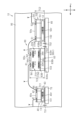
- FIG. 1 is a circuit diagram schematically showing the circuit configuration of the signal transmission device of the first embodiment.
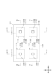
- FIG. 2 is a cross-sectional view schematically showing the cross-sectional structure of the signal transmission device of FIG. 3 is a plan view schematically showing a planar structure of a transformer chip of the signal transmission device of FIG. 2.
- FIG. 4 is a cross-sectional view schematically showing the cross-sectional structure of the transformer chip of FIG. 3 taken along a plane perpendicular to the thickness direction of the transformer chip.
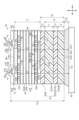
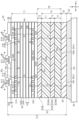
- FIG. 5 is a cross-sectional view schematically showing the cross-sectional structure along line 5-5 of the transformer chip in FIG.
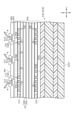
- FIG. 6 is a cross-sectional view schematically showing the cross-sectional structure of the transformer chip of FIG.
- FIG. 7 is a cross-sectional view schematically showing the cross-sectional structure along line 7-7 of the transformer chip in FIG.
- FIG. 8 is a cross-sectional view schematically showing the cross-sectional structure along line 8-8 of the transformer chip of FIG.
- FIG. 9 is an explanatory diagram for explaining an example of a trans-chip manufacturing process.
- FIG. 10 is an explanatory diagram for explaining an example of a trans-chip manufacturing process.
- FIG. 11 is an explanatory diagram for explaining an example of a trans-chip manufacturing process.
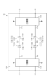
- FIG. 12 is a circuit diagram schematically showing the circuit configuration of the signal transmission device of the second embodiment.
- 13 is a cross-sectional view schematically showing the cross-sectional structure of the signal transmission device of FIG. 12.
- FIG. 14 is a plan view schematically showing a planar structure of a capacitor chip of the signal transmission device of FIG. 13.
- FIG. 15 is a cross-sectional view schematically showing a cross-sectional structure of the capacitor chip of FIG. 14 cut along a plane perpendicular to the thickness direction of the capacitor chip.
- 16 is a cross-sectional view schematically showing the cross-sectional structure of the capacitor chip of FIG. 14 taken along line 16-16.
- 17 is a cross-sectional view schematically showing the cross-sectional structure of the capacitor chip of FIG. 14 taken along line 17-17.
- 18 is a cross-sectional view schematically showing the cross-sectional structure of the capacitor chip of FIG. 14 taken along line 18-18.
- FIG. 19 is a cross-sectional view schematically showing the cross-sectional structure of the capacitor chip of FIG. 14 taken along line 19-19.
- FIG. 20 is a cross-sectional view schematically showing the cross-sectional structure of a transformer chip in the signal transmission device of the modification.
- FIG. 21 is a cross-sectional view schematically showing the cross-sectional structure of a transformer chip in the signal transmission device of the modification.
- FIG. 22 is a cross-sectional view schematically showing a cross-sectional structure of the signal transmission device of the modification taken along a plane perpendicular to the thickness direction of the transformer chip.
- 23 is a plan view schematically showing a planar structure of a transformer chip in the signal transmission device of FIG. 22.
- FIG. FIG. 24 is a cross-sectional view schematically showing a cross-sectional structure of the signal transmission device of the modification taken along a plane perpendicular to the thickness direction of the transformer chip.
- FIG. 1 shows a simplified example of the circuit configuration of the signal transmission device 10. As shown in FIG.
- the signal transmission device 10 is a device that electrically insulates between a primary side terminal 11 and a secondary side terminal 12 while transmitting a pulse signal.
- the signal transmission device 10 is a digital isolator, one example of which is a DC/DC converter.
- the signal transmission device 10 includes a primary circuit 13 electrically connected to a primary terminal 11, a secondary circuit 14 electrically connected to a secondary terminal 12, and a primary circuit 13.
- a signal transmission circuit 10 ⁇ /b>A having a transformer 15 electrically connecting to the secondary side circuit 14 is provided.
- the primary side circuit 13 corresponds to the "first circuit”
- the secondary side circuit 14 corresponds to the "second circuit”.
- the primary side circuit 13 is a circuit configured to operate when a first voltage is applied.
- the primary circuit 13 is electrically connected, for example, to an external control device (not shown).
- the secondary circuit 14 is a circuit configured to operate when a second voltage different from the first voltage is applied.
- the second voltage is higher than the first voltage, for example.
- the first voltage and the second voltage are DC voltages.
- Secondary circuit 14 is electrically connected to, for example, a drive circuit to be controlled by the control device.
- a drive circuit is a switching circuit.
- the signal transmission device 10 transmits the signal from the primary circuit 13 to the secondary circuit 14 via the transformer 15 . is transmitted and a signal is output from the secondary side circuit 14 to the drive circuit via the secondary side terminal 12 .
- the primary side circuit 13 and the secondary side circuit 14 are electrically insulated by the transformer 15 . More specifically, the transformer 15 restricts the transmission of the DC voltage between the primary circuit 13 and the secondary circuit 14, while allowing the transmission of the pulse signal.
- the state in which the primary side circuit 13 and the secondary side circuit 14 are insulated means the state in which the transmission of the DC voltage is interrupted between the primary side circuit 13 and the secondary side circuit 14. This means that the transmission of the pulse signal from the primary side circuit 13 to the secondary side circuit 14 is permitted.
- the secondary circuit 14 is configured to receive signals from the primary circuit 13 .
- the dielectric strength of the signal transmission device 10 is, for example, 2500 Vrms or more and 7500 Vrms or less.
- the dielectric breakdown voltage of the signal transmission device 10 of this embodiment is about 5700 Vrms.
- the specific numerical value of the withstand voltage of the signal transmission device 10 is not limited to this and is arbitrary.
- the ground of the primary side circuit 13 and the ground of the secondary side circuit 14 are provided independently.
- the signal transmission device 10 of this embodiment includes two transformers 15 for transmitting two types of signals from the primary circuit 13 to the secondary circuit 14 . More specifically, the signal transmission device 10 includes a transformer 15 used to transmit a first signal from the primary circuit 13 to the secondary circuit 14 and a second signal from the primary circuit 13 to the secondary circuit 14 . and a transformer 15 used for transmission of two signals.
- the first signal is a signal containing rise information of the external signal input to the signal transmission device 10
- the second signal is a signal containing fall information of the external signal.
- a pulse signal is generated by the first signal and the second signal.
- transformer 15 used for transmitting the first signal is referred to as “transformer 15A”
- transformer 15 used for transmitting the second signal is referred to as “transformer 15B”.
- the transformer 15A corresponds to the "first signal transformer”
- the transformer 15B corresponds to the "second signal transformer”.
- the signal transmission device 10 includes a primary signal line 16A connecting the primary circuit 13 and the transformer 15A, a primary signal line 16B connecting the primary circuit 13 and the transformer 15B, the transformers 15A and 2 A secondary signal line 17A connecting the secondary circuit 14 and a secondary signal line 17B connecting the secondary circuit 14 and the transformer 15B are provided.
- the primary signal line 16A transmits the first signal from the primary circuit 13 to the transformer 15A
- the primary signal line 16B transmits the second signal from the primary circuit 13 to the transformer 15B
- the secondary signal line 17A transmits the first signal from the transformer 15A to the secondary circuit 14, and the secondary signal line 17B transmits the second signal from the transformer 15B to the secondary circuit 14.
- the first signal is transmitted from the primary circuit 13 to the secondary circuit 14 through the primary signal line 16A, the transformer 15A, and the secondary signal line 17A in this order.
- the second signal is transmitted from primary circuit 13 to secondary circuit 14 via primary signal line 16B, transformer 15B, and secondary signal line 17B in this order.
- the transformer 15A transmits the first signal from the primary circuit 13 to the secondary circuit 14 and electrically isolates the primary circuit 13 and the secondary circuit 14 from each other.
- the transformer 15A has a first transformer 21A and a second transformer 22A connected in series.
- the first transformer 21A corresponds to the "first insulating element”
- the second transformer 22A corresponds to the "second insulating element”.
- the signal transmission device 10 includes a pair of connection signal lines 18A and 19A that connect the first transformer 21A and the second transformer 22A.
- a pair of connection signal lines 18A and 19A are signal lines through which a first signal is transmitted.
- the dielectric breakdown voltage of each transformer 21A, 22A in this embodiment is, for example, 2500 Vrms or more and 7500 Vrms or less.
- the dielectric strength of each transformer 21A, 22A may be 2500 Vrms or more and 5700 Vrms or less.
- the specific numerical value of the dielectric strength of each transformer 21A, 22A is not limited to this and is arbitrary.
- the first transformer 21A has a first coil 31A and a second coil 32A that is electrically insulated from the first coil 31A and can be magnetically coupled.
- the second transformer 22A has a first coil 33A and a second coil 34A electrically insulated from and magnetically coupled to the first coil 33A.
- the first coil 31A is connected to the primary side circuit 13 by the primary side signal line 16A, and is also connected to the ground of the primary side circuit 13. That is, the first end of the first coil 31A is electrically connected to the primary circuit 13, and the second end of the first coil 31A is electrically connected to the ground of the primary circuit 13. there is
- the second coil 32A is connected to the second coil 34A by a pair of connection signal lines 18A, 19A.
- the second coil 32A and the second coil 34A are connected together so as to be electrically floating.
- the second coil 32A and the second coil 34A serve as relay coils that relay the transmission of the first signal between the first coil 31A and the first coil 33A.
- the first coil 33A is connected to the secondary circuit 14 by the secondary signal line 17A, and is also connected to the ground of the secondary circuit 14. That is, the first end of the first coil 33A is electrically connected to the secondary circuit 14, and the second end of the first coil 33A is electrically connected to the ground of the secondary circuit 14. there is
- the transformer 15B transmits the second signal from the primary circuit 13 to the secondary circuit 14 and electrically isolates the primary circuit 13 and the secondary circuit 14 from each other.
- the transformer 15B has a first transformer 21B and a second transformer 22B connected in series.
- the first transformer 21B corresponds to the "first insulating element”
- the second transformer 22B corresponds to the "second insulating element”.
- the signal transmission device 10 includes a pair of connection signal lines 18B and 19B that connect the first transformer 21B and the second transformer 22B.
- a pair of connection signal lines 18B and 19B are signal lines for transmitting a second signal.
- the first transformer 21B has a first coil 31B and a second coil 32B that is electrically insulated from the first coil 31B and can be magnetically coupled.
- the second transformer 22B has a first coil 33B and a second coil 34B electrically insulated from the first coil 33B and capable of magnetic coupling.
- the dielectric strength voltage of the first transformer 21B is the same as the dielectric strength voltage of the first transformer 21A
- the dielectric strength voltage of the second transformer 22B is the same as the dielectric strength voltage of the second transformer 22A. Since the connection configuration of the first transformer 21B and the second transformer 22B is the same as the connection configuration of the first transformer 21A and the second transformer 22A, detailed description thereof will be omitted.
- the first signal output from the primary side circuit 13 is transmitted to the secondary side circuit 14 via the first transformer 21A and the second transformer 22A.
- the second signal output from the primary circuit 13 is transmitted to the secondary circuit 14 via the first transformer 21B and the second transformer 22B.
- FIG. 2 shows an example of a schematic cross-sectional structure showing a part of the internal configuration of the signal transmission device 10.
- the signal transmission device 10 is a semiconductor device in which a plurality of semiconductor chips are packaged.
- the package format of the signal transmission device 10 is, for example, an SO (Small Outline) system, and in this embodiment, it is an SOP (Small Outline Package). Note that the package format of the signal transmission device 10 can be arbitrarily changed.
- the signal transmission device 10 includes a first chip 40, a second chip 50, and a transformer chip 60 as semiconductor chips. Further, the signal transmission device 10 includes a primary die pad 70 on which the first chip 40 is mounted, a secondary die pad 80 on which the second chip 50 is mounted, the die pads 70, 80 and the chips 40, 50, and a sealing resin 90 that seals 60 .
- the transformer chip 60 corresponds to the "insulating chip”
- the primary side die pad 70 corresponds to the "first die pad”
- the secondary side die pad 80 corresponds to the "second die pad”.
- the sealing resin 90 is made of an electrically insulating material, such as a black epoxy resin.
- the sealing resin 90 is formed in a rectangular plate shape having a thickness direction in the z direction.
- each die pad 70, 80 is made of a material containing Cu (copper).
- the die pads 70 and 80 may be made of another metal material such as Al (aluminum).
- the material forming each die pad 70, 80 is not limited to a conductive material.
- each die pad 70, 80 may be made of ceramics such as alumina. In other words, each die pad 70, 80 may be made of an electrically insulating material.
- the primary die pad 70 and the secondary die pad 80 are arranged side by side while being separated from each other.
- the direction in which the primary die pads 70 and the secondary die pads 80 are arranged when viewed from the z direction is defined as the x direction.
- a direction perpendicular to the x direction when viewed from the z direction is the y direction.
- the x-direction corresponds to the "first direction” and the y-direction corresponds to the "second direction”.
- Both the primary die pad 70 and the secondary die pad 80 are formed in a flat plate shape.
- the shape of each of the die pads 70 and 80 viewed from the z direction is a rectangular shape with short sides in the x direction and long sides in the y direction.
- the area of the secondary die pad 80 viewed in the z direction is larger than the area of the primary die pad 70 viewed in the z direction.
- the shape of each die pad 70, 80 viewed from the z-direction can be arbitrarily changed.
- the shape of each of the die pads 70 and 80 viewed from the z direction may be a rectangular shape with long sides in the x direction and short sides in the y direction.
- the transformer chip 60 is mounted on the secondary die pad 80 . That is, both the transformer chip 60 and the second chip 50 are mounted on the secondary die pad 80 .
- the transformer chip 60 and the second chip 50 are arranged apart from each other in the x direction on the secondary die pad 80 . Therefore, it can be said that the chips 40, 50, 60 are arranged apart from each other in the x direction.
- the chips 40, 50, 60 are arranged in the order of the first chip 40, the transformer chip 60, and the second chip 50 from the primary die pad 70 toward the secondary die pad 80 in the x direction. ing.
- the transformer chip 60 is arranged between the first chip 40 and the second chip 50 in the x-direction.
- the die pads 70 and 80 are not exposed from the sealing resin 90 .
- the distance between the primary die pad 70 and the secondary die pad 80 in the x direction is greater than the distance between the second chip 50 and the transformer chip 60 in the x direction. big. Therefore, when viewed from the z direction, the distance between the first tip 40 and the transformer chip 60 in the x direction is greater than the distance between the second tip 50 and the transformer tip 60 in the x direction. In other words, the transformer chip 60 is arranged closer to the second chip 50 than to the first chip 40 .
- the shape of the first chip 40 viewed from the z direction is a rectangle having short sides and long sides.
- the first chip 40 is mounted on the primary die pad 70 so that its short sides are along the x-direction and its long sides are along the y-direction.
- the first chip 40 includes a first substrate 43 on which the primary circuit 13 is formed.
- the first substrate 43 is, for example, a semiconductor substrate.
- An example of a semiconductor substrate is a substrate made of a material containing Si (silicon).
- a wiring layer 44 is formed on the first substrate 43 .
- the wiring layer 44 has a plurality of insulating films laminated in the z direction and metal layers provided between insulating films adjacent in the z direction.
- the metal layer constitutes the wiring pattern of the first chip 40 .
- the metal layer is electrically connected to, for example, primary circuit 13 .
- the first chip 40 has a chip main surface 40s and a chip rear surface 40r facing opposite sides in the z-direction.
- the first substrate 43 constitutes the chip rear surface 40r
- the wiring layer 44 constitutes the chip main surface 40s.
- the chip back surface 40 r faces the primary die pad 70 .
- a plurality of first electrode pads 41 and a plurality of second electrode pads 42 are provided on the chip main surface 40 s side of the first chip 40 . More specifically, each electrode pad 41, 42 is provided so as to be exposed from the chip main surface 40s.
- Each electrode pad 41 , 42 is electrically connected to the primary circuit 13 by a wiring layer 44 , for example.
- the plurality of first electrode pads 41 are arranged on the opposite side of the chip main surface 40s from the transformer chip 60 with respect to the center of the chip main surface 40s in the x direction. Although not shown, the plurality of first electrode pads 41 are arranged apart from each other in the y direction. As shown in FIG. 2, the plurality of second electrode pads 42 are arranged closer to the transformer chip 60 with respect to the center of the chip main surface 40s in the x direction in the chip main surface 40s. Although not shown, the plurality of second electrode pads 42 are arranged apart from each other in the y direction.
- the first chip 40 is bonded to the primary die pad 70 with the first bonding material 101 . More specifically, a first bonding material 101 is interposed between the chip rear surface 40r and the primary die pad 70. As shown in FIG. The first bonding material 101 bonds the chip back surface 40 r and the primary die pad 70 .
- the first bonding material 101 is a conductive bonding material such as solder or Ag (silver) paste.
- the first bonding material 101 corresponds to "first conductive bonding material".
- the first bonding material 101 bonds the first substrate 43 of the first chip 40 and the primary side die pad 70 .
- the first substrate 43 and the primary side die pad 70 are electrically connected. Therefore, the primary circuit 13 is electrically connected to the primary die pad 70 via the first bonding material 101 .
- the primary die pad 70 constitutes a ground. Therefore, it can be said that the primary side circuit 13 is electrically connected to the ground.
- the shape of the second chip 50 viewed from the z-direction is a rectangle having short sides and long sides.
- the second chip 50 is mounted on the secondary die pad 80 so that its short sides are along the x-direction and its long sides are along the y-direction.
- the second chip 50 includes a second substrate 53 on which the secondary circuit 14 is formed.
- the second substrate 53 is, for example, a semiconductor substrate.
- An example of a semiconductor substrate is a Si substrate.
- a wiring layer 54 is formed on the second substrate 53 .
- the wiring layer 54 has a plurality of insulating films laminated in the z-direction and metal layers provided between insulating films adjacent in the z-direction.
- the metal layer constitutes the wiring pattern of the second chip 50 .
- the metal layer is electrically connected to secondary circuit 14, for example.
- the second chip 50 has a chip main surface 50s and a chip rear surface 50r facing opposite sides in the z-direction.
- the second substrate 53 constitutes the chip rear surface 50r
- the wiring layer 54 constitutes the chip main surface 50s.
- the chip back surface 50 r faces the secondary die pad 80 .
- the chip rear surface 50 r faces the same side as the chip rear surface 40 r of the first chip 40
- the chip main surface 50 s faces the same side as the chip main surface 40 s of the first chip 40 .
- a plurality of first electrode pads 51 and a plurality of second electrode pads 52 are provided on the chip main surface 50 s side of the second chip 50 . More specifically, each electrode pad 51, 52 is provided so as to be exposed from the chip main surface 50s.
- Each of the electrode pads 51 and 52 is electrically connected to the secondary circuit 14 by a wiring layer 54, for example.
- the plurality of first electrode pads 51 are arranged closer to the transformer chip 60 with respect to the center of the chip main surface 50s in the x direction in the chip main surface 50s. Although not shown, the plurality of first electrode pads 51 are arranged apart from each other in the y direction.
- the plurality of second electrode pads 52 are arranged on the opposite side of the chip main surface 50s from the transformer chip 60 with respect to the center of the chip main surface 50s in the x direction. Although not shown, the plurality of second electrode pads 52 are arranged apart from each other in the y direction.
- the second chip 50 is bonded to the secondary die pad 80 with the second bonding material 102.
- the second bonding material 102 is interposed between the chip rear surface 50r and the secondary die pad 80.
- the second bonding material 102 bonds the chip back surface 50 r and the secondary die pad 80 .
- the second bonding material 102 is a conductive bonding material such as solder or Ag paste.
- the second bonding material 102 is made of the same material as the first bonding material 101, for example.
- the second bonding material 102 corresponds to "second conductive bonding material".
- the second bonding material 102 bonds the second substrate 53 of the second chip 50 and the secondary die pad 80 .
- the second substrate 53 and the secondary die pad 80 are electrically connected. Therefore, the secondary circuit 14 is electrically connected to the secondary die pad 80 via the second bonding material 102 .
- the secondary die pad 80 constitutes a ground. Therefore, it can be said that the secondary circuit 14 is electrically connected to the ground.
- the transformer chip 60 includes both transformers 15A and 15B (see FIG. 1).
- the shape of the transformer chip 60 viewed in the z-direction is a rectangle having short sides and long sides.
- the transformer chip 60 is mounted on the secondary die pad 80 so that the long side extends along the y direction and the short side extends along the x direction when viewed from the z direction.
- the transformer chip 60 has a chip main surface 60s and a chip rear surface 60r facing opposite to each other in the z-direction.
- the chip rear surface 60 r faces the secondary die pad 80 . That is, the chip rear surface 60r faces the same side as the chip rear surface 50r of the second chip 50, and the chip main surface 60s faces the same side as the chip main surface 50s of the second chip 50.
- the transformer chip 60 has a plurality of first electrode pads 61 and a plurality of second electrode pads 62 .
- Each first electrode pad 61 and each second electrode pad 62 are provided on the side of the chip main surface 60s. More specifically, each electrode pad 61, 62 is provided so as to be exposed from the chip main surface 60s when viewed in the z direction.
- the plurality of first electrode pads 61 are arranged near the first chip 40 with respect to the center of the chip main surface 60s in the x direction in the chip main surface 60s.
- the plurality of second electrode pads 62 are arranged closer to the second chip 50 with respect to the center of the chip main surface 60s in the x direction in the chip main surface 60s.
- a plurality of wires W are connected to each of the first chip 40 , the transformer chip 60 and the second chip 50 .
- Each wire W is a bonding wire formed by a wire bonding apparatus, and is made of a conductor such as Au (gold), Al, Cu, or the like.
- a plurality of first electrode pads 41 of the first chip 40 are individually connected by a plurality of wires W to a plurality of primary side leads (not shown).
- the primary lead is a component that constitutes the primary terminal 11 in FIG. Thereby, the primary side circuit 13 and the primary side terminal 11 are electrically connected.
- the primary side lead is made of the same material as the primary side die pad 70 .
- the primary side lead and the primary side die pad 70 may be integrally formed.
- the primary lead is arranged on the side opposite to the secondary die pad 80 with respect to the primary die pad 70 and is formed across the sealing resin 90 .
- the primary lead has a portion that protrudes outward from the sealing resin 90 .
- a portion of the primary lead that protrudes outward from the sealing resin 90 constitutes an external terminal of the signal transmission device 10 .
- a plurality of second electrode pads 42 of the first chip 40 are individually connected to a plurality of first electrode pads 61 of the transformer chip 60 by a plurality of wires W. Thereby, the primary side circuit 13 and each transformer 21A, 21B (see FIG. 1) are electrically connected.
- the wiring layer 44 of the first chip 40, the plurality of second electrode pads 42, the plurality of wires W, and the plurality of first electrode pads 61 are each one of the primary signal lines 16A and 16B (see FIG. 1). make up the department.
- a plurality of second electrode pads 62 of the transformer chip 60 are individually connected to a plurality of first electrode pads 51 of the second chip 50 by a plurality of wires W.
- the transformers 22A and 22B and the secondary side circuit 14 are electrically connected. That is, the plurality of second electrode pads 62, the plurality of wires W, and the plurality of first electrode pads 51 of the second chip 50 respectively constitute part of the secondary signal lines 17A and 17B (see FIG. 1). ing.
- the plurality of second electrode pads 52 of the second chip 50 are individually connected by a plurality of wires W to a plurality of secondary leads (not shown).
- the secondary lead is a component that constitutes the secondary terminal 12 in FIG. Thereby, the secondary circuit 14 and the secondary terminal 12 are electrically connected.
- the secondary lead is made of the same material as the secondary die pad 80 .
- the secondary lead and secondary die pad 80 may be integrally formed.
- the secondary lead is spaced apart from the secondary die pad 80 on the side opposite to the primary die pad 70 and formed across the sealing resin 90 .
- the secondary lead has a portion that protrudes outward from the sealing resin 90 .
- a portion of the secondary lead protruding outward from the sealing resin 90 constitutes an external terminal of the signal transmission device 10 .
- FIG. 3 is a plan view schematically showing the planar structure of the transformer chip 60.
- FIG. 4 is a cross-sectional view schematically showing the cross-sectional structure of the transformer chip 60 taken along the xy plane. In FIG. 4, hatching lines are omitted from the viewpoint of visibility of the drawing.
- 5 and 6 are cross-sectional views schematically showing cross-sectional structures of the transformer chip 60 cut along the yz plane in a state where the transformer chip 60 is mounted on the secondary die pad 80.
- FIG. 7 and 8 are cross-sectional views schematically showing cross-sectional structures of the transformer chip 60 cut along the xz plane in a state where the transformer chip 60 is mounted on the secondary die pad 80.
- FIG. 5 to 8 are schematic cross-sectional structures of the transformer chip 60, and the number of layered element insulating layers 64 to be described later is not limited to the number of layered element insulating layers 64 in FIGS. Also, since the coils 31A, 31B, 32A, 32B, 33A, 33B, 34A, and 34B in FIGS. , 33B, 34A, 34B. 5 to 8, the first end portion 36, which will be described later, is omitted.
- the direction from the chip rear surface 60r of the transformer chip 60 to the chip main surface 60s is defined as upward, and the direction from the chip main surface 60s to the chip rear surface 60r is defined as downward.
- the transformer chip 60 is obtained by integrating both transformers 15A and 15B into one chip. That is, the transformer chip 60 is a chip dedicated to both the transformers 15A and 15B, different from the first chip 40 and the second chip 50.
- FIG. 1 the transformer chip 60 is a chip dedicated to both the transformers 15A and 15B, different from the first chip 40 and the second chip 50.
- both transformers 15A and 15B are arranged apart from each other in the y direction when viewed from the z direction.
- the first transformer 21A of the transformer 15A and the first transformer 21B of the transformer 15B are arranged closer to the first chip 40 (see FIG. 2) than the center of the transformer chip 60 in the x-direction.
- the second transformer 22A of the transformer 15A and the second transformer 22B of the transformer 15B are arranged closer to the second chip 50 (see FIG. 2) than the center of the transformer chip 60 in the x-direction.
- the first transformers 21A and 21B are aligned in the x direction and spaced apart in the y direction.
- the second transformers 22A and 22B are aligned in the x direction and spaced apart in the y direction.
- the first transformer 21A and the second transformer 22A are aligned in the y direction and spaced apart in the x direction.
- the first transformer 21B and the second transformer 22B are aligned in the y direction and spaced apart in the x direction. That is, it can be said that the first transformer 21A (21B) and the second transformer 22A (22B) are spaced apart in the arrangement direction of the die pads 70 and 80.
- the first coil 31A of the first transformer 21A and the first coil 33A of the second transformer 22A are arranged with a gap in the x direction.
- the first coil 31B of the first transformer 21B and the first coil 33B of the second transformer 22B are arranged with a gap in the x direction. That is, the first coil 31A (31B) of the first transformer 21A (21B) and the first coil 33A (33B) of the second transformer 22A (22B) are arranged with a gap in the arrangement direction of the die pads 70 and 80. It can be said that there is
- first coil 31A of the first transformer 21A and the first coil 31B of the first transformer 21B are arranged with a gap in the y direction.
- the first coil 33A of the second transformer 22A and the first coil 33B of the second transformer 22B are arranged with a gap in the y direction. That is, the first coil 31A of the first transformer 21A and the first coil 31B of the first transformer 21B are arranged with a gap in the direction orthogonal to the arrangement direction of the die pads 70 and 80 when viewed from the z direction. It can also be said.
- first coil 33A of the second transformer 22A and the first coil 33B of the second transformer 22B are arranged with a gap in the direction orthogonal to the arrangement direction of the die pads 70 and 80 when viewed from the z direction. It can also be said.
- each coil 31A, 31B, 33A, 33B is one of Ti (titanium), TiN (titanium nitride), Ta (tantalum), TaN (tantalum nitride), Au, Ag, Cu, Al, and W (tungsten) Or a plurality is selected as appropriate.
- each coil 31A, 31B, 33A, 33B is made of a material containing Cu.
- each coil 31A, 31B, 33A, 33B has the same shape.
- Each of the coils 31A, 31B, 33A, and 33B includes a spiral coil portion 35, a first end portion 36 extending inward from the inner peripheral portion of the coil portion 35, and an outer peripheral portion of the coil portion 35. and a second end 37 extending outwardly from the portion.
- a first end 36 of each coil 31A, 31B is an end electrically connected to the primary circuit 13 (see FIG. 1), and a second end 37 of each coil 31A, 31B is connected to the primary circuit. 13 is the end electrically connected to the ground.
- a first end 36 of each coil 33A, 33B is an end electrically connected to the secondary circuit 14 (see FIG. 1), and a second end 37 of each coil 33A, 33B is connected to the secondary circuit. 14 is an end electrically connected to the ground.
- a plurality of (three in this embodiment) first electrode pads 61 are electrically connected to the first coils 31A and 31B individually.
- the plurality of first electrode pads 61 are arranged apart from each other in the y direction.
- the plurality of first electrode pads 61 are arranged at positions overlapping the coil portions 35 of the first coils 31A and 31B when viewed in the y direction.
- the three first electrode pads 61 are referred to as first electrode pads 61A, 61B, 61C.
- the first electrode pads 61A and 61B correspond to the "first pad”
- the first electrode pad 61C corresponds to the "third pad”.
- the first electrode pad 61A When viewed from the z-direction, the first electrode pad 61A is arranged inside the coil portion 35 of the first coil 31A. More specifically, the first electrode pad 61A is arranged with a gap inward from the inner peripheral edge of the coil portion 35 of the first coil 31A. It can be said that the coil portion 35 of the first coil 31A is formed so as to surround the first electrode pad 61A. It can also be said that the first electrode pad 61A is arranged inside the first coil 31A. A first end portion 36 of the first coil 31A is electrically connected to the first electrode pad 61A.
- the first electrode pad 61A is arranged at a position overlapping the first end portion 36 of the first coil 31A when viewed in the y direction. When viewed from the z-direction, the first electrode pads 61A are displaced from the center of the first coil 31A. It can be said that the first electrode pad 61A is arranged at a position not overlapping the center of the first coil 31A when viewed from the z direction.
- the center of the first coil 31A is the center of the coil portion 35 of the first coil 31A. That is, it can be said that the center of the first coil 31A is the winding center of the coil portion 35 of the first coil 31A.
- the first electrode pads 61A are arranged shifted in the y direction with respect to the center of the coil portion 35 of the first coil 31A. More specifically, the first electrode pad 61A is arranged to be shifted toward the first coil 31B with respect to the center of the coil portion 35 of the first coil 31A in the y direction. By arranging the first electrode pads 61A in this manner, it is possible to reduce eddy currents generated in the first electrode pads 61A due to the magnetic flux generated from the first coil 31A.
- the first electrode pad 61B When viewed from the z-direction, the first electrode pad 61B is arranged inside the coil portion 35 of the first coil 31B. More specifically, the first electrode pad 61B is arranged with a gap inward from the inner peripheral edge of the coil portion 35 of the first coil 31B. It can be said that the coil portion 35 of the first coil 31B is formed so as to surround the first electrode pad 61B. It can also be said that the first electrode pad 61B is arranged inside the first coil 31B. A first end portion 36 of the first coil 31B is electrically connected to the first electrode pad 61B.
- the first electrode pad 61B is arranged at a position overlapping the first end 36 of the first coil 31B when viewed in the y direction. When viewed from the z direction, the first electrode pads 61B are arranged to be offset from the center of the first coil 31B. It can also be said that the first electrode pad 61B is arranged at a position not overlapping the center of the first coil 31B when viewed from the z direction.
- the center of the first coil 31B is the center of the coil portion 35 of the first coil 31B. That is, it can be said that the center of the first coil 31B is the winding center of the coil portion 35 of the first coil 31B.
- the first electrode pads 61B are arranged to be shifted in the y direction with respect to the center of the coil portion 35 of the first coil 31B. More specifically, the first electrode pads 61B are arranged to be shifted toward the first coil 31A with respect to the center of the coil portion 35 of the first coil 31B in the y direction. By arranging the first electrode pads 61B in such a manner, it is possible to reduce the eddy current generated in the first electrode pads 61B due to the magnetic flux generated from the first coil 31B.
- the first electrode pad 61C When viewed from the z direction, the first electrode pad 61C is arranged between the coil portion 35 of the first coil 31A and the coil portion 35 of the first coil 31B in the y direction. That is, the first electrode pad 61C is arranged outside the coil portions 35 of the first coils 31A and 31B when viewed in the z direction. It can also be said that the first electrode pad 61C is arranged between the first electrode pads 61A and 61B in the y direction when viewed from the z direction. A second end portion 37 of the first coil 31A and a second end portion 37 of the first coil 31B are electrically connected to the first electrode pad 61C.
- a plurality of (three in this embodiment) second electrode pads 62 are electrically connected to the first coils 33A and 33B individually.
- the plurality of second electrode pads 62 are arranged at positions overlapping the coil portions 35 of the first coils 33A and 33B when viewed in the y direction.
- Each electrode pad 61, 62 is made of a material containing Al, for example.
- the three second electrode pads 62 are referred to as second electrode pads 62A, 62B, 62C.
- the second electrode pads 62A and 62B correspond to the "second pad”
- the second electrode pad 62C corresponds to the "fourth pad”.
- the second electrode pad 62A When viewed from the z direction, the second electrode pad 62A is arranged inside the coil portion 35 of the first coil 33A. More specifically, the second electrode pad 62A is arranged with a gap inward from the inner peripheral edge of the coil portion 35 of the first coil 33A. It can also be said that the coil portion 35 of the first coil 33A is formed so as to surround the second electrode pad 62A. It can also be said that the second electrode pad 62A is arranged inside the first coil 33A. A first end portion 36 of the first coil 33A is electrically connected to the second electrode pad 62A.
- the second electrode pad 62A is arranged at a position overlapping the first end 36 of the first coil 33A when viewed in the y direction. When viewed in the z direction, the second electrode pads 62A are arranged offset from the center of the first coil 33A. It can be said that the second electrode pad 62A is arranged at a position not overlapping the center of the first coil 33A when viewed from the z direction.
- the center of the first coil 33A is the center of the coil portion 35 of the first coil 33A. That is, it can be said that the center of the first coil 33A is the winding center of the coil portion 35 of the first coil 33A.
- the second electrode pads 62A are arranged shifted in the y direction with respect to the center of the coil portion 35 of the first coil 33A. More specifically, the second electrode pad 62A is arranged to be shifted toward the first coil 33B with respect to the center of the coil portion 35 of the first coil 33A in the y direction. By arranging the second electrode pads 62A in such a manner, it is possible to reduce the eddy current generated in the second electrode pads 62A due to the magnetic flux generated from the first coil 33A.
- the second electrode pad 62B When viewed from the z-direction, the second electrode pad 62B is arranged inside the coil portion 35 of the first coil 33B. More specifically, the second electrode pad 62B is arranged with a gap inward from the inner peripheral edge of the coil portion 35 of the first coil 33B. It can also be said that the coil portion 35 of the first coil 33B is formed so as to surround the second electrode pad 62B. It can also be said that the second electrode pad 62B is arranged inside the first coil 33B. A first end portion 36 of the first coil 33B is electrically connected to the second electrode pad 62B.
- the second electrode pad 62B is arranged at a position overlapping the first end 36 of the first coil 33B when viewed in the y direction. When viewed in the z-direction, the second electrode pads 62B are displaced from the center of the first coil 33B. It can be said that the second electrode pad 62B is arranged at a position that does not overlap the center of the first coil 33B when viewed from the z direction.
- the center of the first coil 33B is the center of the coil portion 35 of the first coil 33B. That is, it can be said that the center of the first coil 33B is the winding center of the coil portion 35 of the first coil 33B.
- the second electrode pads 62B are arranged shifted in the y direction with respect to the center of the coil portion 35 of the first coil 33B. More specifically, the second electrode pad 62B is arranged to be shifted toward the first coil 33A with respect to the center of the coil portion 35 of the first coil 33B in the y direction. By arranging the second electrode pads 62B in such a manner, it is possible to reduce the eddy current generated in the second electrode pads 62B due to the magnetic flux generated from the first coil 33B.
- the second electrode pad 62C When viewed from the z direction, the second electrode pad 62C is arranged between the coil portion 35 of the first coil 33A and the coil portion 35 of the first coil 33B in the y direction. That is, the second electrode pad 62C is arranged outside the coil portions 35 of the first coils 33A and 33B when viewed in the z direction. It can also be said that the second electrode pad 62C is arranged between the second electrode pads 62A and 62B in the y direction when viewed from the z direction. The second electrode pad 62C is electrically connected to the second end 37 of the first coil 33A and the second end 37 of the first coil 33B.
- the arrangement of the first electrode pads 61A to 61C and the second electrode pads 62A to 62C is similar to the arrangement of the first electrode pads 61A to 61C and the second electrode pads 62A to 62C shown in FIG. It is not limited and can be changed arbitrarily.
- the first electrode pads 61A when viewed from the z direction, the first electrode pads 61A may be arranged shifted in the x direction with respect to the center of the coil portion 35 of the first coil 31A.
- the first electrode pad 61B and the second electrode pads 62A and 62B can be similarly changed.
- the first electrode pad 61A may be arranged at a position overlapping the coil portion 35 of the first coil 31A when viewed from the z direction.
- the first electrode pad 61B and the second electrode pads 62A and 62B can be similarly changed.
- the second coil 32A of the first transformer 21A is arranged at a position overlapping the first coil 31A of the first transformer 21A when viewed in the z direction.
- the second coil 32B of the first transformer 21B is arranged at a position overlapping the first coil 31B of the first transformer 21B when viewed in the z direction.
- the second coil 34A of the second transformer 22A is arranged at a position overlapping the first coil 33A of the second transformer 22A when viewed in the z direction.
- the second coil 34B of the second transformer 22B is arranged at a position overlapping the first coil 33B of the second transformer 22B when viewed in the z direction.
- the second coils 32A and 34A are arranged with a gap in the x direction.
- the second coil 32B and the second coil 34B are arranged with a gap in the x direction. That is, the second coil 32A (32B) of the first transformer 21A (21B) and the second coil 34A (34B) of the second transformer 22A (22B) are arranged with a gap in the arrangement direction of the die pads 70, 80. It can be said that there is
- the second coil 32A and the second coil 32B are arranged with a gap in the y direction.
- the second coils 34A and 34B are arranged with a gap in the y direction. That is, the second coil 32A of the first transformer 21A and the second coil 32B of the first transformer 21B are arranged with a gap in the direction orthogonal to the arrangement direction of the die pads 70 and 80 when viewed from the z direction. It can also be said.
- the second coil 34A of the second transformer 22A and the second coil 34B of the second transformer 22B are arranged with a gap in the direction perpendicular to the arrangement direction of the die pads 70 and 80 when viewed from the z direction. It can also be said.
- the first end 36 of the second coil 32A and the first end 36 of the second coil 34A are connected to each other, and the second end 37 of the second coil 32A and the second end 37 of the second coil 34A are connected to each other.
- the first end 36 of the second coil 32B and the first end 36 of the second coil 34B are connected to each other, and the second end 37 of the second coil 32B and the second end 37 of the second coil 34B are connected to each other.
- both the first end portion 36 of the second coil 32A and the first end portion 36 of the second coil 34A are the coil portions 35 of the second coils 32A and 34A among the plurality of element insulating layers 64 .
- the first end portions 36 of the second coils 32A and 34A are provided in the element insulating layer 64 closer to the substrate 63 than the coil portions 35 of the second coils 32A and 34A among the plurality of element insulating layers 64. ing.
- both the second end portion 37 of the second coil 32A and the second end portion 37 of the second coil 34A have the same element insulation as the coil portions 35 of the second coils 32A and 34A among the plurality of element insulation layers 64 . It is provided in layer 64 .
- both the first end portion 36 of the second coil 32B and the first end portion 36 of the second coil 34B are the coil portions 35 of the second coils 32B and 34B among the plurality of element insulating layers 64. is provided in the element insulating layer 64 different from the .
- both the second end portion 37 of the second coil 32B and the second end portion 37 of the second coil 34B have the same element insulation as the coil portions 35 of the second coils 32B and 34B among the plurality of element insulation layers 64 . It is provided in layer 64 .
- the arrangement of the first ends 36 and the second ends 37 of the second coils 32B and 34B is the same as the arrangement of the first ends 36 and the second ends 37 of the second coils 32A and 34A.
- the number of turns of the first coil 31A and the number of turns of the second coil 32A are the same. Further, in the present embodiment, the outer diameter of the coil portion 35 of the first coil 31A and the outer diameter of the coil portion 35 of the second coil 32A are equal. Note that the first coil 31B and the second coil 32B, the first coil 33A and the second coil 34A, and the first coil 33B and the second coil 34B also have the same relationship as the first coil 31A and the second coil 32A. be.
- the winding direction of the coil portion 35 of the first coil 31A and the winding direction of the coil portion 35 of the first coil 31B are the same.
- the winding direction of the coil portion 35 of the first coil 33A and the winding direction of the coil portion 35 of the first coil 33B are the same. Therefore, as shown in FIG. 3, the first coil 31A and the first coil 31B are arranged point-symmetrically about the first electrode pad 61C. Further, the first coil 33A and the first coil 33B are arranged so as to be point symmetrical about the second electrode pad 62C.
- the transformer chip 60 has a substrate 63 and an element insulating layer 64 formed on the substrate 63 .
- Substrate 63 is formed of, for example, a semiconductor substrate.
- the substrate 63 is a semiconductor substrate made of a material containing Si.
- the substrate 63 may use a wide bandgap semiconductor or a compound semiconductor as a semiconductor substrate.
- the substrate 63 may be an insulating substrate made of a material containing glass or an insulating substrate made of a material containing ceramics such as alumina.
- a wide bandgap semiconductor is a semiconductor substrate having a bandgap of 2.0 eV or more.
- the wide bandgap semiconductor may be SiC (silicon carbide).
- the compound semiconductor may be a III-V compound semiconductor.
- the compound semiconductor may contain at least one of AlN (aluminum nitride), InN (indium nitride), GaN (gallium nitride), and GaAs (gallium arsenide).
- the substrate 63 includes a body portion 63A and a substrate insulating layer 63B.
- the substrate 63 has a substrate front surface 63s and a substrate rear surface 63r facing opposite sides in the z-direction.
- the substrate front surface 63 s faces the same side as the front surface 64 s of the element insulating layer 64
- the substrate rear surface 63 r faces the same side as the rear surface 64 r of the element insulating layer 64 .
- the body portion 63A has a front surface 63As and a rear surface 63Ar facing opposite sides in the z direction.
- the front surface 63As faces the same side as the front surface 64s of the element insulating layer 64
- the rear surface 63Ar faces the same side as the rear surface 64r of the element insulating layer 64.
- FIG. A rear surface 63Ar of the main body portion 63A constitutes a substrate rear surface 63r of the substrate 63. As shown in FIG.
- the body portion 63A includes a first semiconductor layer 63AA, a second semiconductor layer 63AB, and an oxide film 63AC.
- the first semiconductor layer 63AA and the second semiconductor layer 63AB are made of a material containing Si, for example.
- Oxide film 63AC is a silicon oxide film.
- the oxide film 63AC is arranged between the first semiconductor layer 63AA and the second semiconductor layer 63AB in the z direction.
- the first semiconductor layer 63AA constitutes the front surface 63As of the body portion 63A
- the second semiconductor layer 63AB constitutes the back surface 63Ar of the body portion 63A (substrate back surface 63r of the substrate 63).
- the substrate insulating layer 63B has a front surface 63Bs and a back surface 63Br facing opposite to each other in the z direction.
- the front surface 63Bs faces the same side as the front surface 63As of the body portion 63A
- the rear surface 63Br faces the same side as the rear surface 63Ar of the main body portion 63A.
- the substrate insulating layer 63B is laminated on the main body portion 63A. In this embodiment, the substrate insulating layer 63B is formed on the surface 63As of the body portion 63A. Therefore, the rear surface 63Br of the substrate insulating layer 63B is in contact with the front surface 63As of the main body portion 63A.
- the substrate insulating layer 63B is formed on the first semiconductor layer 63AA. Therefore, the back surface 63Br of the substrate insulating layer 63B is in contact with the first semiconductor layer 63AA.
- a surface 63Bs of the substrate insulating layer 63B constitutes a substrate surface 63s of the substrate 63 .
- the substrate insulating layer 63B includes an oxide film.
- the substrate insulating layer 63B is an LP (Low Pressure)-TEOS (tetraethylorthosilicate) oxide film.
- the TEOS oxide film is a silicon oxide film formed by reaction between an organic TEOS gas and an oxygen-based gas using a low-pressure CVD (Chemical Vapor Deposition) method.
- a plurality of element insulating layers 64 are laminated in the z-direction on the surface 63Bs of the substrate insulating layer 63B.
- the z direction can also be said to be the thickness direction of the element insulating layer 64 .
- the total thickness of the plurality of device insulating layers 64 is thicker than the thickness of the substrate 63 .
- the number of lamination of the element insulating layers 64 is set according to the withstand voltage required for the transformer chip 60 . Therefore, the total thickness of the plurality of element insulating layers 64 may be thinner than the thickness of the substrate 63 depending on the number of stacked element insulating layers 64 .
- the thickness of the substrate 63 is the distance between the front surface 63Bs of the substrate insulating layer 63B and the rear surface 63Ar of the main body portion 63A in the z direction.
- the element insulating layer 64 has a first insulating film 64A and a second insulating film 64B formed on the first insulating film 64A.
- the first insulating film 64A is, for example, an etching stopper film, and is made of a material containing SiN (silicon nitride), SiC, SiCN (nitrogen-added silicon carbide), or the like. Further, the first insulating film 64A has a function of preventing diffusion of Cu, for example. That is, it can be said that the first insulating film 64A is a Cu diffusion prevention film. In this embodiment, the first insulating film 64A is made of a material containing SiN.
- the second insulating film 64B is an interlayer insulating film, for example, and is an oxide film made of a material containing SiO 2 (silicon oxide). As shown in FIGS. 5 and 6, the second insulating film 64B is thicker than the first insulating film 64A.
- the thickness of the first insulating film 64A may be 50 nm or more and less than 1000 nm.
- the thickness of the second insulating film 64B may be 500 nm or more and 5000 nm or less. In this embodiment, the thickness of the first insulating film 64A is, for example, approximately 300 nm, and the thickness of the second insulating film 64B is, for example, approximately 2000 nm.
- a first electrode pad 61 and a second electrode pad 62 are provided on the surface 64 s of the element insulating layer 64 .
- the surface 64s of the element insulating layer 64 is the surface of the uppermost element insulating layer 64 among the plurality of element insulating layers 64 stacked in the z direction.
- the back surface 64 r of the element insulating layer 64 faces the opposite side to the front surface 64 s of the element insulating layer 64 and faces the substrate surface 63 s of the substrate 63 .
- the back surface 64r of the element insulating layer 64 is in contact with the substrate front surface 63s of the substrate 63 .
- the rear surface 64r of the element insulating layer 64 is the rear surface of the lowermost element insulating layer 64 among the plurality of element insulating layers 64 stacked in the z direction.
- the transformer chip 60 further has a protective film 65 formed on the surface 64 s of the element insulating layer 64 and a passivation film 66 formed on the protective film 65 .
- the protective film 65 is a film that protects the element insulating layer 64, and is formed of, for example, a silicon oxide film.
- Passivation film 66 is a surface protective film of transformer chip 60 and is formed of, for example, a silicon nitride film. The passivation film 66 constitutes the chip main surface 60 s of the transformer chip 60 .
- the first electrode pad 61 and the second electrode pad 62 are covered with a protective film 65 and a passivation film 66.
- the protective film 65 and the passivation film 66 are provided with openings for exposing the first electrode pads 61 and the second electrode pads 62 . Therefore, the electrode pads 61 and 62 are provided with exposed surfaces for connecting the wires W to each other.
- the first transformers 21A and 21B are provided within the element insulating layer 64. As shown in FIG. In other words, the first coil 31A and the second coil 32A of the first transformer 21A and the first coil 31B and the second coil 32B of the first transformer 21B are provided inside the element insulating layer 64, respectively.
- the first coil 31A and the second coil 32A of the first transformer 21A are arranged facing each other in the z direction.
- the first coil 31A and the second coil 32A are arranged apart from each other in the z direction.
- One or more element insulating layers 64 are interposed between the first coil 31A and the second coil 32A in the z direction.
- the first coil 31A is positioned closer to the front surface 64s than the rear surface 64r in the element insulating layer 64
- the second coil 32A is positioned closer to the rear surface 64r than the front surface 64s in the element insulating layer 64. That is, the first coil 31A is arranged near the surface 64s with respect to the second coil 32A among the plurality of element insulating layers 64 .
- the second coil 32A is arranged closer to the rear surface 64r than the first coil 31A among the plurality of element insulating layers 64 .
- the first coil 31B and the second coil 32B of the first transformer 21B are arranged facing each other in the z direction.
- the first coil 31B and the second coil 32B are arranged apart from each other in the z direction.
- One or more element insulating layers 64 are interposed between the first coil 31B and the second coil 32B in the z direction.
- the first coil 31B is positioned closer to the front surface 64s than the rear surface 64r in the element insulating layer 64
- the second coil 32B is positioned closer to the rear surface 64r than the front surface 64s in the element insulating layer 64. That is, the first coil 31B is arranged near the surface 64s with respect to the second coil 32B among the plurality of element insulating layers 64 .
- the second coil 32B is arranged closer to the back surface 64r than the first coil 31B among the plurality of element insulating layers 64 .
- the first coils 31A and 31B are arranged at positions aligned with each other in the z direction. In other words, the first coils 31A and 31B are arranged in the same element insulating layer 64 among the plurality of element insulating layers 64 .
- the second coils 32A and 32B are arranged at positions aligned with each other in the z direction. In other words, the second coils 32A and 32B are arranged in the same element insulating layer 64 among the plurality of element insulating layers 64 .
- the second coils 32A and 32B are arranged apart from the back surface 64r of the element insulating layer 64 in the z direction. That is, between the second coils 32A, 32B and the rear surface 64r of the element insulating layer 64, one or more element insulating layers 64 are interposed.
- the first coils 31A and 31B are provided so as to penetrate the element insulating layer 64 of one layer in the z direction. That is, both the first insulating film 64A and the second insulating film 64B of the one-layer element insulating layer 64 are provided with openings for forming the first coils 31A and 31B.
- the first coils 31A and 31B are formed by embedding conductive members made of a material containing Cu in the openings.
- the second coils 32A and 32B are also formed by embedding conductive members made of a material containing Cu in the openings, like the first coils 31A and 31B.
- the material of the second coils 32A, 32B may be different from that of the first coils 31A, 31B.
- the second coils 32A and 32B may be formed by embedding conductive members made of a material containing Al, for example, in the openings.
- the first coil 33A and the second coil 34A of the second transformer 22A are arranged facing each other in the z direction.
- the first coil 33A and the second coil 34A are arranged apart from each other in the z direction.
- One or more element insulating layers 64 are interposed between the first coil 33A and the second coil 34A in the z direction.
- the first coil 33A is positioned closer to the front surface 64s than the rear surface 64r in the element insulating layer 64
- the second coil 34A is positioned closer to the rear surface 64r than the front surface 64s in the element insulating layer 64. That is, the first coil 33A is arranged near the surface 64s with respect to the second coil 34A among the plurality of element insulating layers 64 .
- the second coil 34A is arranged closer to the rear surface 64r than the first coil 33A among the plurality of element insulating layers 64 .
- the first coil 33B and the second coil 34B of the second transformer 22B are arranged facing each other in the z direction.
- the first coil 33B and the second coil 34B are arranged apart from each other in the z direction.
- One or more element insulating layers 64 are interposed between the first coil 33B and the second coil 34B in the z direction.
- the first coil 33B is positioned closer to the front surface 64s than the rear surface 64r in the element insulating layer 64
- the second coil 34B is positioned closer to the rear surface 64r than the front surface 64s in the element insulating layer 64. That is, the first coil 33B is arranged near the surface 64s with respect to the second coil 34B among the plurality of element insulating layers 64 .
- the second coil 34B is arranged closer to the rear surface 64r than the first coil 33B among the plurality of element insulating layers 64 .
- the first coils 33A and 33B are arranged at positions aligned with each other in the z direction. In other words, the first coils 33A and 33B are arranged in the same element insulating layer 64 among the plurality of element insulating layers 64 .
- the second coils 34A and 34B are arranged at positions aligned with each other in the z direction. In other words, the second coils 34A and 34B are arranged in the same element insulating layer 64 among the plurality of element insulating layers 64 .
- the second coils 34A and 34B are arranged apart from the rear surface 64r of the element insulating layer 64 in the z direction.
- the first coils 33A, 33B and the first coils 31A, 31B are arranged at positions aligned with each other in the z direction.
- the second coils 34A, 34B and the second coils 32A, 32B are arranged at positions aligned with each other in the z direction.
- the first coils 31A and 31B correspond to the "first surface side conductive portion” and the "first surface side coil”
- the second coils 32A and 32B correspond to the "first back side conductive portion”. and “first back side coil”.
- the first coils 33A, 33B correspond to the "second surface-side conductive portion” and the “second surface-side coil”
- the second coils 34A, 34B correspond to the "second back-side conductive portion” and the "second back-side coil.” corresponds to
- the first end 36 of the first coil 31A has a portion facing the first electrode pad 61A in the z direction.
- a first end portion 36 of the first coil 31A is connected to the first electrode pad 61A by a connection line 67A.
- the connection line 67A is a via that penetrates the element insulating layer 64 in the z-direction, and one or more of Ti, TiN, Ta, TaN, Au, Ag, Cu, Al, and W are appropriately selected, for example.
- the connection line 67A is made of W, Ti, or TiN.
- the connection line 67A is arranged at a position overlapping both the first end 36 of the first coil 31A and the first electrode pad 61A. 61A and extends in the z-direction.
- the first end 36 of the first coil 31B has a portion facing the first electrode pad 61B in the z direction.
- a first end portion 36 of the first coil 31B is connected to the first electrode pad 61B by a connection line 67B.
- connection line 67B As shown in FIG. 5, the material and connection manner of connection line 67B are similar to the material and connection manner of connection line 67A.
- connection line 68A is a via that penetrates the element insulating layer 64 in the z-direction, for example, like the connection line 67A, and is one of Ti, TiN, Ta, TaN, Au, Ag, Cu, Al, and W, for example. Or a plurality is selected as appropriate.
- the connection line 68A is made of the same material as the connection line 67A.
- connection line 68A When viewed from the z-direction, the connection line 68A is arranged at a position overlapping both the second ends 37 of the first coils 31A and 31B and the first electrode pads 61C. It extends in the z direction so as to connect with the electrode pad 61C.
- connection line 67C As shown in FIGS. 3 and 6, the first end 36 of the first coil 33A has a portion facing the second electrode pad 62A in the z direction. A first end portion 36 of the first coil 33A is connected to the second electrode pad 62A by a connection line 67C. As shown in FIG. 6, the material and connection manner of connection line 67C are similar to the material and connection manner of connection line 67A (see FIG. 5).
- the first end 36 of the first coil 33B has a portion facing the second electrode pad 62B in the z direction.
- a first end portion 36 of the first coil 33B is connected to the second electrode pad 62B by a connection line 67D.
- the material and connection manner of the connection line 67D are similar to the material and connection manner of the connection line 67A.
- the second end 37 of the first coil 33A and the second end 37 of the first coil 33B have portions facing the second electrode pad 62C in the z direction.
- the second ends 37 of the first coils 33A, 33B are connected to the second electrode pad 62C by a connecting wire 68B.
- the material and connection manner of connection line 68B are similar to the material and connection manner of connection line 68A (see FIG. 5).
- the transformer chip 60 is bonded to the secondary die pad 80 with the third bonding material 103 . More specifically, the third bonding material 103 is interposed between the rear surface 63Ar (chip rear surface 60r) of the main body portion 63A of the substrate 63 and the secondary die pad 80. As shown in FIG. The third bonding material 103 bonds the back surface 63Ar (chip back surface 60r) of the main body 63A and the secondary die pad 80 . In this embodiment, the third bonding material 103 is in contact with the entire rear surface 63Ar (chip rear surface 60r) of the main body 63A.
- the third bonding material 103 is an insulating bonding material such as epoxy resin.
- the third bonding material 103 is made of a material different from that of the first bonding material 101 and the second bonding material 102 (see FIG. 2 for both).
- the third bonding material 103 corresponds to "bonding material”.
- the thickness TC3 of the transformer chip 60 is thicker than the thickness TC1 of the first chip 40 and the thickness TC2 of the second chip 50 .
- the thickness TC3 of the transformer chip 60 is the distance between the chip main surface 60s and the chip rear surface 60r of the transformer chip 60 in the z direction.
- the thickness TC1 of the first chip 40 is the distance between the chip main surface 40s and the chip rear surface 40r of the first chip 40 in the z direction.
- the thickness TC2 of the second chip 50 is the distance between the chip main surface 50s and the chip rear surface 50r of the second chip 50 in the z direction.
- the thickness TS3 of the third bonding material 103 is equal to the thickness TS1 of the first bonding material 101 and the thickness TS2 of the second bonding material 102 .
- the thickness TS3 of the third bonding material 103 corresponds to "the thickness of the bonding material”.
- the thickness TS3 of the third bonding material 103 is the distance between the secondary die pad 80 and the chip rear surface 60r of the transformer chip 60 in the z direction.
- the thickness TS1 of the first bonding material 101 is the distance between the primary die pad 70 and the chip rear surface 40r of the first chip 40 in the z direction.
- the thickness TS2 of the second bonding material 102 is the distance between the secondary die pad 80 and the chip rear surface 50r of the second chip 50 in the z direction. Further, if the difference between the thickness TS3 of the third bonding material 103 and the thickness TS1 of the first bonding material 101 is, for example, within 20% of the thickness TS3 of the third bonding material 103, the thickness of the third bonding material 103 is It can be said that the thickness TS3 and the thickness TS1 of the first bonding material 101 are equal.
- the thickness of the third bonding material 103 is, for example, within 20% of the thickness TS3 of the third bonding material 103, the thickness of the third bonding material 103 is It can be said that the thickness TS3 and the thickness TS2 of the second bonding material 102 are equal.
- the height position of the chip main surface 60s of the transformer chip 60 is higher than both the height position of the chip main surface 40s of the first chip 40 and the height position of the chip main surface 50s of the second chip 50.
- the thickness of the first substrate 43 of the first chip 40 is equal to the thickness TB of the substrate 63 (see FIG. 5).
- the thickness of the second substrate 53 of the second chip 50 is equal to the thickness TB of the substrate 63 .
- the thickness TB of the substrate 63 is thinner than the thickness TT of the plurality of element insulating layers 64 .
- the thickness TB of the substrate 63 is thicker than the distance D1 between the first coil 31A (31B) and the second coil 32A (32B) in the z direction.
- a distance D1 between the first coil 31A (31B) and the second coil 32A (32B) in the z direction is a distance D2 between the second coil 32A (32B) and the back surface 64r of the element insulating layer 64 in the z direction. bigger than The distance D2 can also be said to be the distance between the second coil 32A (32B) and the substrate surface 63s of the substrate 63 in the z direction.
- a distance D1 between the first coil 31A (31B) and the second coil 32A (32B) in the z direction is a distance D3 between the first coil 31A (31B) and the surface 64s of the element insulating layer 64 in the z direction. bigger than
- the first coil 33A (33B) is provided at the same position as the first coil 31A (31B) in the z direction
- the second coil 34A (34B) is provided at the same position as the second coil 32A (32B) in the z direction. Therefore, the distance between the first coil 33A (33B) and the second coil 34A (34B) in the z direction is equal to the distance D1. Also, the distance between the second coil 34A (34B) and the back surface 64r of the element insulating layer 64 in the z direction is equal to the distance D2. Also, the distance between the first coil 33A (33B) and the surface 64s of the element insulating layer 64 in the z direction is equal to the distance D3.
- the thickness TZ of the substrate insulating layer 63B of the transformer chip 60 is thicker than the thickness TA of one element insulating layer 64 and thinner than the thickness TT of the plurality of element insulating layers 64 .
- the thickness TZ of the substrate insulating layer 63B is the distance between the front surface 63Bs and the back surface 63Br of the substrate insulating layer 63B in the z direction.
- the thickness TA of one layer of the element insulating layer 64 is the distance between the back surface of the first insulating film 64A and the front surface of the second insulating film 64B in the one layer of the element insulating layer 64 in the z direction.
- the thickness TT of the plurality of element insulating layers 64 is the distance between the front surface 64s and the rear surface 64r of the element insulating layers 64 in the z direction.
- the thickness TZ of the substrate insulating layer 63B is equal to that of each of the coils 31A to 34A and 31B to It can be said that it is thicker than each thickness of 34B.
- the thickness TZ of the substrate insulating layer 63B is equal to or greater than the distance D2 between the second coil 32A (32B) and the back surface 64r of the element insulating layer 64 in the z direction. In one example, the thickness TZ of the substrate insulating layer 63B is 2 ⁇ m or more and 4 ⁇ m or less. A distance D2 between the second coil 32A (32B) and the back surface 64r of the element insulating layer 64 in the z direction is 0.5 ⁇ m or more and 2 ⁇ m or less. In this embodiment, the thickness TZ of the substrate insulating layer 63B is thicker than the distance D2 between the second coil 32A (32B) and the back surface 64r of the element insulating layer 64 in the z direction.
- the thickness TZ of the substrate insulating layer 63B is equal to or greater than the distance D3 between the first coil 31A (31B) and the surface 64s of the element insulating layer 64 in the z direction.
- the thickness TZ of the substrate insulating layer 63B is thinner than the distance D1 between the first coil 31A (31B) and the second coil 32A (32B) in the z direction.
- the thickness TZ of the substrate insulating layer 63B is thinner than the thickness T4 of the main body portion 63A.
- the thickness T4 of the body portion 63A is the distance between the front surface 63As and the back surface 63Ar of the body portion 63A in the z direction.
- the thickness TZ of the substrate insulating layer 63B is thinner than half the thickness T4 of the main body portion 63A.
- the thickness TZ of the substrate insulating layer 63B is thinner than 1/3 of the thickness T4 of the main body portion 63A.
- the thickness T1 of the first semiconductor layer 63AA is thicker than the thickness T2 of the second semiconductor layer 63AB and the thickness T3 of the oxide film 63AC.
- the thickness T2 of the second semiconductor layer 63AB is thicker than the thickness T3 of the oxide film 63AC.
- the thickness T1 of the first semiconductor layer 63AA is the distance between the front surface of the first semiconductor layer 63AA in contact with the substrate insulating layer 63B and the rear surface thereof in contact with the oxide film 63AC in the z direction.
- the thickness T2 of the second semiconductor layer 63AB is the distance in the z direction between the surface of the second semiconductor layer 63AB in contact with the oxide film 63AC and the back surface facing in the z direction opposite to this surface.
- the thickness T3 of the oxide film 63AC is the distance in the z direction between the surface of the oxide film 63AC in contact with the first semiconductor layer 63AA and the back surface in contact with the second semiconductor layer 63AB.
- the thickness TZ of the substrate insulating layer 63B is thinner than the thickness T1 of the first semiconductor layer 63AA.
- the thickness TZ of the substrate insulating layer 63B is thinner than the thickness T2 of the second semiconductor layer 63AB.
- the thickness TZ of the substrate insulating layer 63B is equal to the thickness T3 of the oxide film 63AC.
- the thickness TZ of the substrate insulating layer 63B is oxidized. It can be said to be equal to the thickness T3 of the membrane 63AC.
- the thickness TZ of the substrate insulating layer 63B is equal to or greater than the thickness TC of the protective film 65. Also, the thickness TZ of the substrate insulating layer 63B is equal to or less than the thickness TD of the passivation film 66 .
- the thickness of the protective film 65 is the distance between the front surface and the rear surface of the protective film 65 in the z direction.
- the surface of the protective film 65 is the surface in contact with the passivation film 66
- the back surface of the protective film 65 is the surface in contact with the element insulating layer 64 .
- the thickness of the passivation film 66 is the distance between the front surface and the back surface of the passivation film 66 in the z direction.
- the front surface of the passivation film 66 constitutes the chip main surface 60 s of the transformer chip 60
- the back surface of the passivation film 66 is the surface in contact with the protective film 65 .
- the thickness TZ of the substrate insulating layer 63B is thinner than the thickness TS3 of the third bonding material 103.
- a thickness TS3 of the third bonding material 103 is less than 10 ⁇ m (approximately 5 ⁇ m). Since the thickness TS3 of the third bonding material 103 is equal to the thickness TS1 of the first bonding material 101 and the thickness TS2 of the second bonding material 102, the thickness TZ of the substrate insulating layer 63B is equal to the thickness of the first bonding material 101. It can also be said that the thickness TZ of the substrate insulating layer 63B is thinner than the thickness TS2 of the second bonding material 102 .
- the method of manufacturing the signal transmission device 10 includes a preparation step of preparing the transformer chip 60 , the first chip 40 , the second chip 50 , the primary die pad 70 and the secondary die pad 80 .
- the transformer chip 60 is manufactured, for example, as follows. As shown in FIG. 9, first, an SOI wafer 630 is prepared as a semiconductor wafer. The SOI wafer 630 constitutes the main body portion 63A of the substrate 63. As shown in FIG. The SOI wafer 630 has a wafer front surface 630s and a wafer rear surface 630r facing opposite sides in the thickness direction. Subsequently, an insulating film 631 is formed on the outer surface of the SOI wafer 630 . The insulating film 631 is formed by reaction between an organic TEOS gas and an oxygen-based gas using, for example, low-pressure CVD.
- FIG. 9 shows a step of forming substrate insulating layers (insulating films 631) on both sides of a semiconductor wafer (SOI wafer 630) in the substrate insulating layer forming step.
- an element insulating layer 640, first transformers 21A and 21B, and second transformers 22A and 22B are formed on the insulating film 631 formed on the wafer surface 630s of the SOI wafer 630.
- the element insulating layer 640 is an insulating layer forming the element insulating layer 64 of the transformer chip 60, and is formed over the entire surface of the insulating film 631 formed on the wafer surface 630s of the SOI wafer 630, for example.
- a plurality of element insulating layers 640 are laminated on the insulating film 631, and the second openings are formed in the element insulating layers 640 in which the second coils 32A, 32B, 34A, and 34B of the transformers 21A, 21B, 22A, and 22B are arranged.
- Element insulating layer 640 is formed by plasma CVD, for example. Since the element insulating layer 640 is formed by plasma CVD, its film quality is different from that of the insulating film 631 formed by low pressure CVD. Then, the second coils 32A, 32B, 34A, 34B are formed by providing the second conductive material in the second openings. In this embodiment, Cu is used as the second conductive material.
- the element insulating layer 640 is laminated again so as to cover the second coils 32A, 32B, 34A, 34B, and the first openings are formed in the element insulating layer 640 where the first coils 31A, 31B, 33A, 33B are arranged.
- the first coils 31A, 31B, 33A and 33B are formed by providing the first conductive material in the first openings.
- Cu is used as the first conductive material.
- an element insulating layer 640 is laminated so as to cover the first coils 31A, 31B, 33A, 33B.
- the method for manufacturing the transformer chip 60 includes the step of laminating the element insulating layer 640 including both insulating elements (both transformers 21A, 21B, 22A, 22B) on the surface of the substrate insulating layer (insulating film 631). .
- a plurality of first electrode pads 61 and a plurality of second electrode pads 62 are formed on the surface of the device insulating layer 640 .
- a protective film 650 and a passivation film 660 are laminated in this order on the surface of the element insulating layer 640 .
- Protective film 650 is a film forming protective film 65 of transformer chip 60 , and is formed over the entire surface of element insulating layer 640 , for example.
- Passivation film 660 is a film forming passivation film 66 of transformer chip 60 , and is formed over the entire surface of protective film 650 , for example.
- a protective film 650 and a passivation film 660 are formed in a state of covering a part of each first electrode pad 61 and a part of each second electrode pad 62 with a mask, for example. and remove the mask. As a result, the electrode pads 61 and 62 are exposed.
- the SOI wafer 630 is ground so that the thickness of the SOI wafer 630 falls within a preset thickness range.
- An insulating film 631 formed on the wafer rear surface 630r of the SOI wafer 630 is ground.
- the insulating film 631 formed on the wafer rear surface 630r of the SOI wafer 630 is removed.
- the wafer rear surface 630r of the SOI wafer 630 may also be ground.
- the sum of the thickness of the SOI wafer 630 and the thickness of the insulating film 631 becomes equal to the thickness TB of the substrate 63 .
- FIG. 11 shows a step of removing the substrate insulating layer (insulating film 631) on the back surface (wafer back surface 630r) of the semiconductor wafer (SOI wafer 630) in the substrate insulating layer forming step. That is, in the present embodiment, the step of removing the substrate insulating layer (insulating film 631) on the rear surface (wafer rear surface 630r) of the semiconductor wafer (SOI wafer 630) is performed after the device insulating layer 640 is laminated.
- the SOI wafer 630 on which the element insulating layer 640, the protective film 650, and the passivation film 660 are formed is cut along the z-direction to singulate the transformer chips 60 . Thereby, a substrate 63, an element insulating layer 64, a protective film 65, and a passivation film 66 are formed. Through the steps described above, the transformer chip 60 is manufactured.
- the substrate insulating layer (insulating film 631) may be formed by thermally oxidizing a semiconductor wafer (SOI wafer 630). Thermal oxidation also forms substrate insulating layers (insulating films 631) on both sides of the semiconductor wafer (SOI wafer 630), so warping of the semiconductor wafer (SOI wafer 630) can be suppressed. Even in this case, the insulating film 631 is different in film quality from the element insulating layer 640 .
- the order of steps for removing the substrate insulating layer (insulating film 631) on the back surface (wafer back surface 630r) of the semiconductor wafer (SOI wafer 630) can be arbitrarily changed.
- the method of manufacturing the signal transmission device 10 includes steps of mounting the first chip 40 on the primary die pad 70 and mounting both the transformer chip 60 and the second chip 50 on the secondary die pad 80 .
- the first chip 40 is mounted on the primary side die pad 70 by die bonding
- both the second chip 50 and the transformer chip 60 are mounted on the secondary side die pad 80 by die bonding.
- the first bonding material 101 is applied on the primary die pad 70
- the second bonding material 102 is applied on the secondary die pad 80 where the second chip 50 is to be mounted
- a third bonding material 103 is applied to a portion of the secondary die pad 80 where the transformer chip 60 is to be mounted.
- the first chip 40 is placed on the first joint material 101
- the second chip 50 is placed on the second joint material 102
- the transformer chip 60 is placed on the third joint material 103 .
- each bonding material 101 to 103 is solidified.
- a conductive bonding material is used for both the first bonding material 101 and the second bonding material 102
- an insulating bonding material is used for the third bonding material 103
- the first bonding material 101 and the second bonding material The solidification method of the material 102 and the solidification method of the third bonding material 103 are different.
- the first bonding material 101 and the second bonding material 102 are heated and cooled, respectively. solidified.
- the third bonding material 103 is made of a material containing epoxy resin
- the third bonding material 103 is solidified by mixing the epoxy resin with a curing agent, for example.
- the transformer chip 60 may be mounted on the secondary die pad 80 .
- the first bonding material 101 is applied on the primary die pad 70
- the second bonding material 102 is applied on the secondary die pad 80 where the second chip 50 is to be mounted.
- the first chip 40 is placed on the first bonding material 101 and the second chip 50 is placed on the second bonding material 102 .
- the first bonding material 101 and the second bonding material 102 are solidified.
- a third bonding material 103 is applied to a portion of the secondary die pad 80 where the transformer chip 60 is to be mounted.
- the transformer chip 60 is placed on the third bonding material 103 .
- the third bonding material 103 is solidified.
- the manufacturing method of the signal transmission device 10 includes a step of forming the wire W.
- a wire W is formed by a wire bonding apparatus. More specifically, wires W are formed to individually connect the plurality of first electrode pads 41 of the first chip 40 and the plurality of primary leads. Wires W are formed for individually connecting the plurality of second electrode pads 52 of the second chip 50 and the plurality of secondary leads. wires W individually connecting the plurality of second electrode pads 42 of the first chip 40 and the plurality of first electrode pads 61 of the transformer chip 60; the plurality of second electrode pads 62 of the transformer chip 60 and the second chip 50; and wires W for individually connecting the plurality of first electrode pads 51 are formed.
- the method of manufacturing the signal transmission device 10 includes a step of forming the sealing resin 90.
- Sealing resin 90 is formed by transfer molding, for example. Thereby, each chip 40, 50, 60, each die pad 70, 80, and each wire W are sealed. Each primary side lead and each secondary side lead are provided so that a part of them protrudes from the side surface of the sealing resin 90 .
- the portions of the plurality of primary leads protruding from the sealing resin 90 and the portions of the plurality of secondary leads protruding from the sealing resin 90 are bent. form the external terminals of the signal transmission device 10 .
- the signal transmission device 10 is manufactured.
- the method for manufacturing one signal transmission device 10 has been described above, the method is not limited to this, and a plurality of signal transmission devices 10 may be manufactured at the same time.
- the transformer chip 60 of this embodiment includes a first transformer 21A (21B) and a second transformer 22A (22B) connected in series.
- the distance D1 between the first coil 31A (31B) and the second coil 32A (32B) of the first transformer 21A (21B) in the z direction and the first coil 33A ( 33B) and the distance D1 between the second coils 34A (34B) in the z direction the dielectric strength of the transformer chip 60 can be improved.
- the first transformer 21A (21B) is electrically connected to the primary side circuit 13 via the wire W
- the second transformer 22A (22B) is electrically connected to the secondary side circuit 14 and the wire. are electrically connected via W. Therefore, when the transformer chip 60 is mounted on the conductive secondary die pad 80, it is necessary to electrically insulate between the transformers 21A (21B), 22A (22B) and the secondary die pad 80. .
- the dielectric breakdown voltage between the transformers 21A (21B), 22A (22B) and the secondary die pad 80 is 2 It is mainly set according to the distance between the following die pad 80 and the z-direction. That is, as the distance between the second coils 32A (32B), 34A (34B) and the secondary die pad 80 in the z direction increases, the transformers 21A (21B), 22A (22B) and the secondary die pad 80 Withstand voltage increases.
- the distance between the second coils 32A (32B), 34A (34B) of the transformers 21A (21B), 22A (22B) and the secondary die pad 80 in the z direction is It is determined by the sum of the distance between 34A (34B) and the main body portion 63A of the substrate 63, the thickness of the substrate 63, and the thickness TS3 of the bonding material 103.
- the coils 32A (32B) and 34A (34B) are arranged below the respective second coils 32A (32B) and 34A (34B).
- the substrate 63 of the transformer chip 60 includes a substrate insulating layer 63B formed on the surface 63As of the main body portion 63A.
- both the element insulating layer 64 and the substrate insulating layer 63B are interposed.
- the coils are arranged below the respective second coils 32A (32B) and 34A (34B).
- the signal transmission device 10 includes the first chip 40 including the primary circuit 13, the primary die pad 70 on which the first chip 40 is mounted, the transformer chip 60, and the transformer chip 60. It comprises a second chip 50 including a secondary circuit 14 configured to receive signals from the primary circuit 13, and a secondary die pad 80 on which the second chip 50 is mounted.
- the transformer chip 60 includes a substrate 63 , an element insulating layer 64 having a surface 64 s and a back surface 64 r opposite to the surface 64 s and closer to the substrate 63 than the surface 64 s , and provided in the element insulating layer 64 .
- the first transformer 21A (21B) includes a first coil 31A (31B) arranged closer to the surface 64s than the back surface 64r in the element insulating layer 64 and a back surface 64r closer to the surface 64s than the surface 64s in the element insulating layer 64. and a second coil 32A (32B) arranged in the .
- the second transformer 22A (22B) includes the first coil 33A (33B) arranged closer to the surface 64s than the back surface 64r in the element insulating layer 64 and the back surface 64r closer to the surface 64s than the surface 64s in the element insulating layer 64.
- the substrate 63 includes a body portion 63A and a substrate insulating layer 63B formed on the surface 63As of the body portion 63A.
- the element insulating layer 64 is laminated on the surface 63Bs of the substrate insulating layer 63B.
- both the element insulating layer 64 and the substrate insulating layer 63B are interposed between the body portion 63A and the second coils 32A (32B) and 34A (34B).
- the coils below the respective second coils 32A (32B) and 34A (34B) are provided. It is possible to avoid increasing the number of stacked element insulating layers 64 near the substrate 63 .
- the main body 63A and the second coils 32A (32B), 34A (34B) ) in the z direction can be increased.
- the distance D4 in the z direction from the next die pad 80 can be increased. Therefore, it is possible to improve the withstand voltage between the second coils 32A (32B), 34A (34B) and the secondary die pad 80 in the z direction. Therefore, it is possible to improve the withstand voltage of the signal transmission device 10 .
- the thickness TZ of the substrate insulating layer 63B is thinner than the thickness T4 of the main body portion 63A.
- the substrate insulating layer 63B can be formed more easily than when the thickness TZ of the substrate insulating layer 63B is equal to or greater than the thickness T4 of the main body portion 63A. That is, the formation time of the substrate insulating layer 63B can be shortened. Therefore, the manufacturing cost of the transformer chip 60 can be reduced.
- the main body portion 63A includes a first semiconductor layer 63AA in contact with the element insulating layer 64, an oxide film 63AC provided on the opposite side of the first semiconductor layer 63AA from the element insulating layer 64, and an oxide film 63AC. and a second semiconductor layer 63AB provided on the side opposite to the first semiconductor layer 63AA with respect to 63AC.
- the distance between the second coils 32A (32B), 34A (34B) and the secondary die pad 80 in the z direction is reduced. dielectric strength is improved. Therefore, it is possible to improve the withstand voltage of the signal transmission device 10 .
- the thickness T1 of the first semiconductor layer 63AA is thicker than both the thickness T3 of the oxide film 63AC and the thickness T2 of the second semiconductor layer 63AB.
- the thickness TZ of the substrate insulating layer 63B is thinner than the thickness T1 of the first semiconductor layer 63AA.
- the substrate insulating layer 63B can be formed more easily than when the thickness TZ of the substrate insulating layer 63B is equal to or greater than the thickness T1 of the first semiconductor layer 63AA. That is, the formation time of the substrate insulating layer 63B can be shortened. Therefore, the manufacturing cost of the transformer chip 60 can be reduced.
- the thickness T2 of the second semiconductor layer 63AB is thicker than the thickness T3 of the oxide film 63AC.
- the thickness TZ of the substrate insulating layer 63B is thinner than the thickness T2 of the second semiconductor layer 63AB.
- the thickness TZ of the substrate insulating layer 63B is equal to or larger than the distance D2 between the second coils 32A (32B), 34A (34B) and the back surface 64r of the element insulating layer 64 in the z direction.
- the substrate insulating layer 63B is a TEOS oxide film.
- the distance between the second coils 32A (32B), 34A (34B) and the secondary die pad 80 in the z direction can be increased without increasing the distance D2.
- the TEOS oxide film is formed on both surfaces of the semiconductor wafer (SOI wafer 630) forming the main body 63A during the manufacturing process of the transformer chip 60. As shown in FIG. Therefore, an increase in the thickness TT of the element insulating layer 64 can be suppressed, and warpage of the semiconductor wafer (SOI wafer 630) forming the substrate 63 during the manufacture of the transformer chip 60 can be suppressed.
- the thickness TZ of the substrate insulating layer 63B is thinner than the thickness TS3 of the third bonding material 103. According to this configuration, the substrate insulating layer 63B can be formed more easily than when the thickness TZ of the substrate insulating layer 63B is equal to or greater than the thickness TS3 of the third bonding material 103 . That is, the formation time of the substrate insulating layer 63B can be shortened. Therefore, the manufacturing cost of the transformer chip 60 can be reduced.
- the third bonding material 103 has electrical insulation.
- the third bonding material 103 and the secondary die pad 80 are not electrically connected. Electrical insulation between the second coils 32A (32B) and 34A (34B) and the secondary die pad 80 is required instead of the electrical insulation between the two coils. Therefore, it is possible to easily improve the withstand voltage of the transformer chip 60 .
- the thickness TZ of the substrate insulating layer 63B is thinner than the thickness TS1 of the first bonding material 101; With this configuration, the substrate insulating layer 63B can be formed more easily than when the thickness TZ of the substrate insulating layer 63B is equal to or greater than the thickness TS1 of the first bonding material 101 . That is, the formation time of the substrate insulating layer 63B can be shortened. Therefore, the manufacturing cost of the transformer chip 60 can be reduced.
- the thickness TZ of the substrate insulating layer 63B is thinner than the thickness TS2 of the second bonding material 102 .
- the substrate insulating layer 63B can be formed more easily than when the thickness TZ of the substrate insulating layer 63B is equal to or greater than the thickness TS2 of the second bonding material 102 . That is, the formation time of the substrate insulating layer 63B can be shortened. Therefore, the manufacturing cost of the transformer chip 60 can be reduced.
- the thickness TZ of the substrate insulating layer 63B is thinner than the distance D1 between the first coil 31A (31B) and the second coil 32A (32B) in the z direction. In other words, the distance D1 between the first coil 31A (31B) and the second coil 32A (32B) is greater than the thickness TZ of the substrate insulating layer 63B.
- the thickness TZ of the substrate insulating layer 63B is thinner than the distance D1 between the first coil 33A (33B) and the second coil 34A (34B) in the z direction. In other words, the distance D1 between the first coil 33A (33B) and the second coil 34A (34B) in the z direction is greater than the thickness TZ of the substrate insulating layer 63B.
- the distance D1 between the first coil 31A (31B) and the second coil 32A (32B) and the distance D1 between the first coil 33A (33B) and the second coil 34A (34B) and can be increased, the dielectric strength of the transformer chip 60 can be improved.
- the distance D1 between the first coil 31A (31B) and the second coil 32A (32B) in the z direction and the distance D1 between the first coil 33A (33B) and the second coil 34A (34B) in the z direction are equal to each other.
- the total dielectric strength voltage of the first and second transformers connected in series is It may be lower than the sum with the dielectric strength voltage.
- the dielectric strength voltage of the first transformer 21A (21B) and the dielectric strength voltage of the second transformer 22A (22B) are equal to each other. Therefore, the total withstand voltage of the first transformer 21A (21B) and the second transformer 22A (22B) connected in series is equal to the withstand voltage of the first transformer 21A (21B) and the withstand voltage of the second transformer 22A (22B) It is roughly equal to the sum of the insulation voltage and the dielectric strength. Therefore, compared to the case where the dielectric strength voltage of the first transformer 21A (21B) and the dielectric strength voltage of the second transformer 22A (22B) are different from each other, the dielectric strength voltage of the transformer chip 60 can be improved.
- the second coil 32A (32B) and the second coil 34A (34B) are arranged at the same position in the z direction. According to this configuration, since the second coil 32A (32B) and the second coil 34A (34B) connected to each other are not shifted in the z direction, the second coil 32A (32B) and the second coil 32A (32B) connected to each other are not shifted. Two coils 34A (34B) can be easily formed in the element insulating layer 64. FIG.
- the first coil 31A (31B) and the first coil 33A (33B) are arranged apart from each other in the x direction, and the second coil 32A (32B) and the second coil 34A (34B) are spaced apart from each other in the x-direction.
- the first coil 31A (33A) and the first coil 31B (33B) are arranged apart from each other in the y direction, and the second coil 32A (34A) and the second coil 32B (34B) are arranged apart from each other in the y direction. are spaced apart.
- the first coil 31A (31B) electrically connected to the primary side circuit 13 is arranged near the first chip 40 in the x direction, and the first coil 31A (31B) electrically connected to the secondary side circuit 14 33A (33B) are arranged near the second chip 50 in the x-direction.
- the wire W can easily connect the first chip 40 including the primary circuit 13 and the first coil 31A (31B). Also, the wire W can easily connect the second chip 50 including the secondary circuit 14 and the first coil 33A (33B).
- the first electrode pad 61A When viewed from the z direction, the first electrode pad 61A is arranged inside the coil portion 35 of the first coil 31A, and the first electrode pad 61B is arranged inside the coil portion 35 of the first coil 31B. placed inside.
- the first electrode pad 61C is arranged at a position overlapping the first coil 31A (31B) in the x direction when viewed from the y direction.
- the second electrode pad 62A is arranged inside the coil portion 35 of the first coil 33A, and the second electrode pad 62B is arranged inside the coil portion 35 of the first coil 33B.
- the second electrode pad 62C is arranged at a position overlapping the first coil 33A (33B) in the x direction when viewed in the y direction.
- the first electrode pads 61A to 61C are arranged closer to the first chip 40 than the first coil 31A (31B) when viewed from the z direction, and the second electrode pads 62A to 62C are arranged to be closer to the first coil 31A (31B).
- the size of the transformer chip 60 can be reduced in the x direction.
- the transformer chip 60 includes a substrate 63, an element insulating layer 64 having a front surface 64s and a rear surface 64r opposite to the front surface 64s and closer to the substrate 63 than the front surface 64s, and an element insulating layer 64, and has a first transformer 21A (21B) and a second transformer 22A (22B) for transmitting signals.
- the first transformer 21A (21B) includes a first coil 31A (31B) arranged closer to the surface 64s than the back surface 64r in the element insulating layer 64 and a back surface 64r closer to the surface 64s than the surface 64s in the element insulating layer 64. and a second coil 32A (32B) arranged in the .
- the second transformer 22A (22B) includes the first coil 33A (33B) arranged closer to the surface 64s than the back surface 64r in the element insulating layer 64 and the back surface 64r closer to the surface 64s than the surface 64s in the element insulating layer 64. and a second coil 34A (34B) arranged in the .
- the second coil 32A (32B) and the second coil 34A (34B) are electrically connected.
- the substrate 63 includes a body portion 63A and a substrate insulating layer 63B formed on the surface 63As of the body portion 63A.
- the element insulating layer 64 is laminated on the surface 63Bs of the substrate insulating layer 63B.
- the thickness TT of the element insulating layer 64 is not increased. It is possible to increase the distance between the body portion 63A and the second coils 32A (32B) and 34A (34B) in the z direction. As a result, the distance between the second coils 32A (32B), 34A (34B) and the chip rear surface 60r of the transformer chip 60 in the z direction can be increased without increasing the thickness TT of the element insulating layer 64. can be done. Therefore, when the transformer chip 60 is mounted on a metal frame, the distance between the second coils 32A (32B), 34A (34B) and the frame in the z direction can be increased. It is possible to improve the withstand voltage.
- the method of manufacturing the transformer chip 60 includes a substrate insulating layer forming step of forming a substrate insulating layer (insulating film 631) on a wafer surface 630s of a semiconductor wafer (SOI wafer 630) constituting the main body 63A; and laminating an element insulating layer 640 including both transformers 21A, 21B, 22A and 22B on the surface of the film 631.
- the substrate insulating layer forming step includes a step of forming insulating films 631 on both the wafer front surface 630 s and the wafer rear surface 630 r of the SOI wafer 630 and a step of removing the insulating film 631 from the wafer rear surface 630 r of the SOI wafer 630 .
- the insulating film 631 is formed on both the wafer front surface 630s and the wafer rear surface 630r of the SOI wafer 630, so that warping of the SOI wafer 630 can be suppressed even if the thickness of the insulating film 631 is increased.
- the insulating film 631 suppresses the thickness of the element insulating layer 640 from increasing, warping of the SOI wafer 630 can be reduced even if the element insulating layer 640 is stacked.
- FIG. 10 of the present embodiment is mainly different from the signal transmission device 10 of the first embodiment in that the transformer chip 60 is replaced with a capacitor chip 120 including a capacitor 110 .
- points different from the first embodiment will be described in detail, and constituent elements common to the first embodiment will be assigned the same reference numerals, and descriptions thereof will be omitted.
- FIG. 12 is a schematic circuit diagram of the signal transmission device 10 of this embodiment.
- the signal transmission circuit 10A of the signal transmission device 10 includes a capacitor 110 as an insulation structure for electrically insulating the primary side circuit 13 and the secondary side circuit 14 from each other.
- the capacitor 110 has a capacitor 110A connected to the signal line that transmits the first signal, and a capacitor 110B connected to the signal line that transmits the second signal. Both capacitors 110A and 110B are provided between primary circuit 13 and secondary circuit 14 .
- the first signal and the second signal are the same as the first signal and the second signal of the first embodiment.
- the capacitor 110A corresponds to the "first signal capacitor”
- the capacitor 110B corresponds to the "second signal capacitor”.
- the signal transmission circuit 10A has a connection signal line 20A as a signal line for transmitting the first signal and a connection signal line 20B as a signal line for transmitting the second signal.
- the connection signal line 20A is provided between the primary signal line 16A and the secondary signal line 17A.
- the connection signal line 20B is provided between the primary signal line 16B and the secondary signal line 17B. That is, the signal lines that transmit the first signal include the primary signal line 16A, the secondary signal line 17A, and the connection signal line 20A.
- the signal lines that transmit the second signal include the primary signal line 16B, the secondary signal line 17B, and the connection signal line 20B.
- the capacitor 110A has a first capacitor 111A and a second capacitor 112A that are connected in series with each other via a connection signal line 20A.
- the first capacitor 111A is electrically connected to the primary side circuit 13 and the second capacitor 112A is electrically connected to the secondary side circuit 14 . More specifically, first capacitor 111A has first electrode 113A and second electrode 114A, and second capacitor 112A has first electrode 115A and second electrode 116A.
- a first electrode 113A of the first capacitor 111A is connected to the primary circuit 13 by a primary signal line 16A, and a second electrode 114A is connected to a second electrode 116A of the second capacitor 112A through a connection signal line 20A. It is connected.
- a first electrode 115A of the second capacitor 112A is connected to the secondary circuit 14 by a secondary signal line 17A. Therefore, the primary side circuit 13 and the secondary side circuit 14 transmit the first signal via the first capacitor 111A and the second capacitor 112A that are connected in series with each other.
- the capacitor 110B has a first capacitor 111B and a second capacitor 112B that are connected in series with each other via the connection signal line 20B.
- the first capacitor 111B has a first electrode 113B and a second electrode 114B
- the second capacitor 112B has a first electrode 115B and a second electrode 116B.
- the configuration of the capacitor 110B and the connection configuration between the capacitor 110B and the primary circuit 13 and the secondary circuit 14 are the same as those of the capacitor 110A, so detailed description thereof will be omitted.
- Primary side circuit 13 and secondary side circuit 14 transmit a second signal via first capacitor 111B and second capacitor 112B that are connected in series with each other.
- the first capacitors 111A and 111B correspond to the "first insulating element”
- the second capacitors 112A and 112B correspond to the "second insulating element”.
- FIG. 13 is a schematic cross-sectional view of part of the signal transmission device 10 of this embodiment.
- the signal transmission device 10 includes a capacitor chip 120 instead of the transformer chip 60 (see FIG. 2) of the first embodiment.
- Capacitor chip 120 like transformer chip 60, is arranged between first chip 40 and second chip 50 in the x-direction. Similar to the transformer chip 60 of the first embodiment, in this embodiment, the distance between the capacitor chip 120 and the second chip 50 in the x direction is equal to the distance between the capacitor chip 120 and the first chip 40 in the x direction. less than distance.
- the capacitor chip 120 is mounted on the secondary die pad 80 .
- the capacitor chip 120 is bonded to the secondary die pad 80 with the third bonding material 103 .
- the third bonding material 103 is a bonding material having electrical insulation, as in the first embodiment.
- the capacitor chip 120 corresponds to an "insulating chip".
- FIG. FIG. 14 is a plan view schematically showing the planar structure of capacitor chip 120.
- FIG. 15 is a cross-sectional view schematically showing the cross-sectional structure of the inside of the capacitor chip 120 taken along the xy plane. In FIG. 15, hatching lines are omitted from the viewpoint of visibility of the drawing.
- 16 to 19 show the cross-sectional structure of the capacitor chip 120 mounted on the secondary die pad 80.
- FIG. 16 to 19 are schematic cross-sectional structures of the capacitor chip 120, and the number of laminated element insulating layers 64 is not limited to the number of laminated element insulating layers 64 in FIGS. 16 to 19, the first end portion 36 is omitted.
- the capacitor chip 120 has a chip main surface 120s and a chip rear surface 120r facing opposite sides in the z direction.
- the chip main surface 120 s faces the same side as the chip main surface 40 s of the first chip 40
- the chip rear surface 120 r faces the same side as the chip rear surface 40 r of the first chip 40 .
- the direction from the chip rear surface 120r to the chip main surface 120s of the capacitor chip 120 is defined as upward
- the direction from the chip main surface 120s to the chip rear surface 120r is defined as downward.
- the capacitor chip 120 includes both capacitors 110A and 110B, and more specifically, both capacitors 110A and 110B are integrated into one chip. That is, the capacitor chip 120 is a chip dedicated to both the capacitors 110A and 110B, which is separate from the first chip 40 and the second chip 50. FIG.
- Both capacitors 110A and 110B are arranged apart from each other in the y direction.
- the first capacitor 111A of the capacitor 110A and the first capacitor 111B of the capacitor 110B are arranged closer to the first chip 40 (see FIG. 13) than the center of the capacitor chip 120 in the x-direction.
- the second capacitor 112A of the capacitor 110A and the second capacitor 112B of the capacitor 110B are arranged closer to the second chip 50 (see FIG. 13) than the center of the capacitor chip 120 in the x direction.
- the first capacitors 111A and 111B are aligned in the x direction and spaced apart in the y direction.
- the second capacitors 112A and 112B are aligned in the x direction and spaced apart in the y direction.
- the first capacitor 111A and the second capacitor 112A are aligned in the y direction and spaced apart in the x direction.
- the first capacitor 111B and the second capacitor 112B are aligned in the y direction and spaced apart in the x direction. That is, it can be said that the first capacitor 111A (111B) and the second capacitor 112A (112B) are spaced apart in the arrangement direction of the die pads 70 and 80.
- the first electrode plate 121A of the first capacitor 111A and the first electrode plate 123A of the second capacitor 112A are arranged with a gap in the x direction. .
- the first electrode plate 121B of the first capacitor 111B and the first electrode plate 123B of the second capacitor 112B are arranged with a gap in the x direction. That is, the first electrode plate 121A (121B) of the first capacitor 111A (111B) and the first electrode plate 123A (123B) of the second capacitor 112A (112B) are arranged with a gap in the array direction of the die pads 70 and 80. It can be said that they are arranged.
- the first electrode plate 121A of the first capacitor 111A and the first electrode plate 121B of the first capacitor 111B are arranged with a gap in the y direction.
- the first electrode plate 123A of the second capacitor 112A and the first electrode plate 123B of the second capacitor 112B are arranged with a gap in the y direction. That is, the first electrode plate 121A of the first capacitor 111A and the first electrode plate 121B of the first capacitor 111B are arranged with a gap in the direction orthogonal to the arrangement direction of the die pads 70 and 80 when viewed from the z direction.
- first electrode plate 123A of the second capacitor 112A and the first electrode plate 123B of the second capacitor 112B are arranged with a gap in the direction perpendicular to the arrangement direction of the die pads 70 and 80 when viewed from the z direction. It can be said that there is
- the first electrode plates 121A, 121B, 123A, and 123B are arranged at positions aligned with each other in the z direction.
- One or more of Ti, TiN, Ta, TaN, Au, Ag, Cu, Al, and W (tungsten) is appropriately selected for each of the first electrode plates 121A, 121B, 123A, and 123B.
- each of the first electrode plates 121A, 121B, 123A, 123B is made of a material containing Cu.
- the first electrode plates 121A, 121B, 123A, 123B have the same shape.
- each of the first electrode plates 121A, 121B, 123A, and 123B is formed in a plate shape with the z direction as the thickness direction.
- Each of the first electrode plates 121A, 121B, 123A, and 123B viewed from the z direction has a rectangular shape with short sides in the x direction and long sides in the y direction.
- the capacitor chip 120 includes a plurality of (two in this embodiment) first electrode pads 131 and a plurality of (two in this embodiment) second electrode pads 132. .
- the plurality of first electrode pads 131 are individually electrically connected to the first capacitors 111A and 111B.
- the plurality of first electrode pads 131 are arranged apart from each other in the y direction.
- the two first electrode pads 131 are referred to as first electrode pads 131A and 131B for convenience.
- the first electrode pads 131A and 131B correspond to "first pads”.
- the first electrode pad 131A When viewed from the z-direction, the first electrode pad 131A is arranged at a position overlapping with the first electrode plate 121A, and the first electrode pad 131B is arranged at a position overlapping with the first electrode plate 121B.
- the first electrode pad 131A is arranged at a position overlapping the center of the first electrode plate 121A in the x direction and the y direction when viewed from the z direction.
- the first electrode pad 131B When viewed from the z-direction, the first electrode pad 131B is arranged at a position overlapping the center of the first electrode plate 121B in the x-direction and the y-direction.
- the first electrode pad 131A is electrically connected to the first electrode plate 121A
- the first electrode pad 131B is electrically connected to the first electrode plate 121B.
- the plurality of second electrode pads 132 are individually electrically connected to the second capacitors 112A and 112B.
- the plurality of second electrode pads 132 are arranged apart from each other in the y direction.
- the two second electrode pads 132 are referred to as second electrode pads 132A and 132B for convenience.
- the second electrode pads 132A and 132B correspond to "second pads”.
- the second electrode pad 132A When viewed from the z-direction, the second electrode pad 132A is arranged at a position overlapping with the first electrode plate 123A, and the second electrode pad 132B is arranged at a position overlapping with the first electrode plate 123B.
- the second electrode pad 132A is arranged at a position overlapping the center of the first electrode plate 123A in the x direction and the y direction when viewed from the z direction.
- the second electrode pad 132B When viewed from the z-direction, the second electrode pad 132B is arranged at a position overlapping the center of the first electrode plate 123B in the x-direction and the y-direction.
- the second electrode pad 132A is electrically connected to the first electrode plate 123A
- the second electrode pad 132B is electrically connected to the first electrode plate 123B.
- the second electrode plate 122A of the first capacitor 111A is arranged at a position overlapping the first electrode plate 121A of the first capacitor 111A when viewed in the z direction.
- the second electrode plate 122B of the first capacitor 111B is arranged at a position overlapping the first electrode plate 121B of the first capacitor 111B when viewed in the z direction.
- the second electrode plate 124A of the second capacitor 112A is arranged at a position overlapping the first electrode plate 123A of the second capacitor 112A when viewed in the z direction.
- the second electrode plate 124B of the second capacitor 112B is arranged at a position overlapping the first electrode plate 123B of the second capacitor 112B when viewed in the z direction.
- the second electrode plates 122A and 124A are arranged with a gap in the x direction.
- the second electrode plate 122B and the second electrode plate 124B are arranged with a gap in the x direction. That is, the second electrode plate 122A (122B) of the first capacitor 111A (111B) and the second electrode plate 124A (124B) of the second capacitor 112A (112B) are spaced apart in the arrangement direction of the die pads 70 and 80. It can be said that they are arranged.
- the second electrode plate 122A and the second electrode plate 122B are arranged with a gap in the y direction.
- the second electrode plate 124A and the second electrode plate 124B are arranged with a gap in the y direction. That is, the second electrode plate 122A of the first capacitor 111A and the second electrode plate 122B of the first capacitor 111B are arranged with a gap in the direction perpendicular to the arrangement direction of the die pads 70 and 80 when viewed from the z direction.
- the second electrode plate 124A of the second capacitor 112A and the second electrode plate 124B of the second capacitor 112B are arranged with a gap in the direction perpendicular to the arrangement direction of the die pads 70 and 80 when viewed from the z direction. It can be said that there is
- the second electrode plate 122A and the second electrode plate 124A are electrically connected to each other. More specifically, the second electrode plate 122A and the second electrode plate 124A are connected by a connection line 140A.
- the connection line 140A is provided between the second electrode plate 122A and the second electrode plate 124A in the x direction and extends along the x direction.
- the connection line 140A is provided in the same element insulating layer 64 among the plurality of element insulating layers 64 as the element insulating layer 64 on which the second electrode plates 122A and 124A are provided.
- connection lines 140A and 140B are made of a material containing Al, for example. Note that the connection lines 140A and 140B are not limited to Al as long as they are made of any conductive material.
- the capacitor chip 120 has a substrate 63 and an element insulating layer 64, like the transformer chip 60 of the first embodiment.
- the configurations of the substrate 63 and the element insulating layer 64 are the same as in the first embodiment.
- the capacitor chip 120 has a protective film 65 and a passivation film 66, like the transformer chip 60 of the first embodiment.
- the structures of the protective film 65 and the passivation film 66 are the same as in the first embodiment.
- the first electrode pads 131 and the second electrode pads 132 are exposed in the z direction from the protective film 65 and the passivation film 66 as in the first embodiment.
- the first capacitors 111A, 111B and the second capacitors 112A, 112B are provided in the element insulating layer 64 respectively.
- the electrode plate 124A and the first electrode plate 123B and the second electrode plate 124B of the second capacitor 112B are provided in the element insulating layer 64, respectively.
- the first electrode plate 121A and the second electrode plate 122A of the first capacitor 111A are arranged to face each other in the z direction.
- the first electrode plate 121A and the second electrode plate 122A are spaced apart in the z direction.
- One or more element insulating layers 64 are interposed between the first electrode plate 121A and the second electrode plate 122A.
- the first electrode plate 121A is arranged closer to the front surface 64s than the rear surface 64r of the element insulating layer 64
- the second electrode plate 122A is arranged closer to the rear surface 64r than the front surface 64s of the element insulating layer 64.
- the first electrode plate 121A is arranged near the surface 64s with respect to the second electrode plate 122A among the plurality of element insulating layers 64 .
- the second electrode plate 122A is arranged closer to the rear surface 64r than the first electrode plate 121A among the plurality of element insulating layers 64 .
- the first electrode plates 121A and 121B are arranged at positions aligned with each other in the z direction. In other words, the first electrode plates 121A and 121B are arranged on the same element insulating layer 64 among the plurality of element insulating layers 64 .
- the second electrode plates 122A and 122B are arranged at positions aligned with each other in the z direction. In other words, the second electrode plates 122A and 122B are arranged on the same element insulating layer 64 among the plurality of element insulating layers 64 .
- the second electrode plates 122A and 122B are arranged apart from the rear surface 64r of the element insulating layer 64 in the z direction. That is, between the second electrode plates 122A, 122B and the rear surface 64r of the element insulating layer 64, one or more element insulating layers 64 are interposed.
- the first electrode plates 121A and 121B are provided so as to penetrate the one-layer element insulating layer 64 in the z-direction. That is, both the first insulating film 64A and the second insulating film 64B of the one-layer element insulating layer 64 are provided with openings for forming the first electrode plates 121A and 121B.
- the first electrode plates 121A and 121B are formed by embedding conductive members made of a material containing Cu in the openings.
- the second electrode plates 122A, 122B are formed similarly to the first electrode plates 121A, 121B.
- the first electrode plate 123A and the second electrode plate 124A of the second capacitor 112A are arranged to face each other in the z direction.
- the first electrode plate 123A and the second electrode plate 124A are arranged apart from each other in the z direction.
- One or more element insulating layers 64 are interposed between the first electrode plate 123A and the second electrode plate 124A in the z direction.
- the first electrode plate 123A is arranged closer to the front surface 64s than the rear surface 64r in the element insulating layer 64
- the second electrode plate 124A is arranged closer to the rear surface 64r than the surface 64s in the element insulating layer 64.
- the first electrode plate 123A is arranged near the surface 64s with respect to the second electrode plate 124A among the plurality of element insulating layers 64 .
- the second electrode plate 124A is arranged closer to the rear surface 64r than the first electrode plate 123A among the plurality of element insulating layers 64 .
- the first electrode plate 123B and the second electrode plate 124B of the second capacitor 112B are arranged to face each other in the z direction.
- the first electrode plate 123B and the second electrode plate 124B are arranged apart from each other in the z direction.
- One or more element insulating layers 64 are interposed between the first electrode plate 123B and the second electrode plate 124B in the z direction.
- the first electrode plate 123B is arranged closer to the front surface 64s than the rear surface 64r in the element insulating layer 64
- the second electrode plate 124B is arranged closer to the rear surface 64r than the front surface 64s in the element insulating layer 64.
- the first electrode plate 123B is arranged near the surface 64s with respect to the second electrode plate 124B among the plurality of element insulating layers 64 .
- the second electrode plate 124B is arranged closer to the rear surface 64r than the first electrode plate 123B among the plurality of element insulating layers 64 .
- the first electrode plates 123A and 123B are arranged at positions aligned with each other in the z direction. In other words, the first electrode plates 123A and 123B are arranged on the same element insulating layer 64 among the plurality of element insulating layers 64 .
- the second electrode plates 124A and 124B are arranged at positions aligned with each other in the z direction. In other words, the second electrode plates 124A and 124B are arranged on the same element insulating layer 64 among the plurality of element insulating layers 64 .
- the second electrode plates 124A and 124B are arranged apart from the rear surface 64r of the element insulating layer 64 in the z direction. That is, between the second electrode plates 124A, 124B and the rear surface 64r of the element insulating layer 64, one or more element insulating layers 64 are interposed.
- first electrode plates 123A, 123B and the first electrode plates 121A, 121B are arranged at positions aligned with each other in the z direction.
- the second electrode plates 124A, 124B and the second electrode plates 122A, 122B are arranged at positions aligned with each other in the z direction.
- the first electrode plates 123A, 123B and the second electrode plates 124A, 124B are formed similarly to the first electrode plates 121A, 121B and the second electrode plates 122A, 122B.
- the first electrode plates 121A and 121B correspond to the "first front side conductive portion” and the “first front side electrode plate”
- the second electrode plates 122A and 122B correspond to the "first back side conductive portion”. It corresponds to "conductive part” and “first back side electrode plate”.
- the first electrode plates 123A and 123B correspond to the "second surface-side conductive portion” and the “second surface-side electrode plate”
- the second electrode plates 124A and 124B correspond to the "second back-side conductive portion" and the "second back-side electrode plate”. side electrode plate”.
- connection line 141A The first electrode plate 121A and the first electrode pad 131A are connected by a connection line 141A.
- the first electrode plate 121B and the first electrode pad 131B are connected by a connection line 141B.
- the first electrode plate 123A and the second electrode pad 132A are connected by a connection line 142A.
- the first electrode plate 123B and the second electrode pad 132B are connected by a connection line 142B.
- Each connection line 141A, 141B, 142A, 142B is a via that penetrates the element insulating layer 64 in the z-direction, and includes, for example, one or more of Ti, TiN, Au, Ag, Cu, Al, and W (tungsten). is selected as appropriate.
- the substrate 63 of the capacitor chip 120 includes a substrate insulating layer 63B provided on the surface 63As of the body portion 63A of the substrate 63, like the transformer chip 60 of the first embodiment. Also, the capacitor chip 120 is bonded to the secondary die pad 80 by the third bonding material 103, like the transformer chip 60 of the first embodiment. Note that the dimensional relationship in the signal transmission device 10 of the present embodiment is the same as the dimensional relationship in the signal transmission device 10 of the first embodiment. However, the distance D1 is the distance between the first electrode plate 121A (121B) and the second electrode plate 122A (122B) in the z direction, and the distance between the first electrode plate 123A (123B) and the second electrode plate 124A (124A).
- the distance D2 be the distance between the second electrode plate 122A (122B, 124A, 124B) and the back surface 64r of the element insulating layer 64 in the z direction.
- Each of the above-described embodiments is an example of the possible forms of the signal transmission device and the insulating tip related to the present disclosure, and is not intended to limit the forms.
- a signal transmission device and an insulating tip related to the present disclosure may take forms different from those exemplified in the above embodiments.
- One example is a form in which a part of the configuration of each of the above embodiments is replaced, changed, or omitted, or a form in which a new configuration is added to each of the above embodiments.
- each of the following modifications can be combined with each other as long as they are not technically inconsistent.
- the same reference numerals as those in each of the above-described embodiments are attached to the portions common to each of the above-described embodiments, and the description thereof is omitted.
- the configuration of the substrate 63 of the transformer chip 60 can be arbitrarily changed.
- the main body portion 63A of the substrate 63 may be a single-layer semiconductor substrate instead of the SOI substrate.
- the thickness TZ of the substrate insulating layer 63B is thinner than the thickness T4 of the main body portion 63A.
- the transformer chip 60 is formed on the rear surface 63Ar of the main body portion 63A of the substrate 63 (the surface of the second semiconductor layer 63AB opposite to the oxide film 63AC in the z direction). It may have a back insulating layer 69 provided. In this embodiment, the back surface insulating layer 69 is formed over the entire surface of the back surface 63Ar of the main body portion 63A.
- the back insulating layer 69 has a front surface 69s and a back surface 69r facing opposite sides in the z-direction. A surface 69s of the back surface insulating layer 69 is in contact with the back surface 63Ar of the main body portion 63A.
- a rear surface 69 r of the rear insulating layer 69 constitutes a chip rear surface 60 r of the transformer chip 60 .
- the back insulating layer 69 is made of an electrically insulating material.
- the back insulating layer 69 is formed of a layer containing SiO, for example.
- the back surface insulating layer 69 is formed by applying, for example, a thermosetting organic siloxane polymer solution having siloxane bonds (Si--O--Si) in the main chain to the back surface 63r of the substrate and solidifying it.
- back surface insulating layer 69 may be formed of a layer containing resin, for example. Examples of resins are epoxy resins, phenolic resins and polyimide resins.
- the transformer chip 60 is bonded to the secondary die pad 80 with the third bonding material 103 . More specifically, the third bonding material 103 is interposed between the rear surface 69r (chip rear surface 60r) of the rear surface insulating layer 69 and the secondary die pad 80. As shown in FIG. The third bonding material 103 bonds the rear surface 69 r (chip rear surface 60 r ) of the rear insulating layer 69 and the secondary die pad 80 . In this embodiment, the third bonding material 103 is in contact with the entire back surface 69r of the back surface insulating layer 69 (chip back surface 60r).
- the thickness TR of the back insulating layer 69 is thicker than the thickness TA of one element insulating layer 64 and thinner than the thickness TT of the plurality of element insulating layers 64 .
- the thickness TR of the back insulating layer 69 is the distance between the front surface 69s and the back surface 69r of the back insulating layer 69 in the z direction.
- the thickness TR of the back insulating layer 69 is equal to that of each of the coils 31A to 34A and 31B to It can be said that it is thicker than each thickness of 34B.
- the thickness TR of the back surface insulating layer 69 is thicker than the distance D2 between the second coil 32A (32B) and the back surface 64r of the element insulating layer 64 in the z direction.
- the thickness TR of the back insulating layer 69 is thicker than the distance D3 between the first coil 31A (31B) and the surface 64s of the element insulating layer 64 in the z direction.
- the thickness TR of the back insulating layer 69 is thinner than the distance D1 between the first coil 31A (31B) and the second coil 32A (32B) in the z direction.
- the thickness TR of the back insulating layer 69 is thinner than the thickness T4 of the substrate 63 .
- the thickness TR of the back insulating layer 69 is thicker than the thickness TC of the protective film 65 . Further, the thickness TR of the back insulating layer 69 is thicker than the thickness TD of the passivation film 66 .
- the thickness TC of the protective film 65 is the distance between the front surface and the rear surface of the protective film 65 in the z direction.
- the surface of the protective film 65 is the surface in contact with the passivation film 66
- the back surface of the protective film 65 is the surface in contact with the element insulating layer 64 .
- the thickness TD of the passivation film 66 is the distance between the front surface and the back surface of the passivation film 66 in the z direction.
- the front surface of the passivation film 66 constitutes the chip main surface 60 s of the transformer chip 60
- the back surface of the passivation film 66 is the surface in contact with the protective film 65 .
- the thickness TR of the back insulating layer 69 is thicker than the thickness TS3 of the third bonding material 103 .
- the thickness TR of the back insulating layer 69 is 5 ⁇ m or more and 100 ⁇ m or less. Since the thickness TS3 of the third bonding material 103 is equal to the thickness TS1 of the first bonding material 101 and the thickness TS2 of the second bonding material 102, the thickness TR of the back insulating layer 69 is equal to the thickness of the first bonding material 101. It can be said that the thickness TR of the back surface insulating layer 69 is thicker than the thickness TS1 of the second bonding material 102 .
- the distance between the second coil 32A (32B) and the secondary die pad 80 in the z direction can be increased compared to a transformer chip that does not have the back insulating layer 69. Therefore, it is possible to improve the withstand voltage between the transformer chip 60 and the secondary die pad 80, so that the withstand voltage of the signal transmission device 10 can be improved.
- the transformer chip 60 may include a back surface insulating layer 69 provided on the back surface 63Ar of the main body portion 63A of the substrate 63.
- the positions of the first electrode pads 61A and 61B of the transformer chip 60 can be arbitrarily changed when viewed from the z direction.
- the first electrode pad 61A may be arranged outside the coil portion 35 of the first coil 31A.
- the first electrode pad 61A may be arranged at a position overlapping the coil portion 35 of the first coil 31A in the x direction when viewed from the y direction.
- the first electrode pad 61A may be arranged closer to the first chip 40 or closer to the second chip 50 in the x direction than the coil portion 35 of the first coil 31A when viewed from the z direction.
- the first electrode pad 61A may be arranged on the side opposite to the first coil 33A in the x direction with respect to the first coil 31A when viewed in the z direction.
- the first electrode pad 61B may be arranged outside the coil portion 35 of the first coil 31B. In this case, the first electrode pad 61B may be arranged at a position overlapping the coil portion 35 of the first coil 31B in the x direction when viewed from the y direction.
- the first electrode pad 61B may be arranged closer to the first chip 40 or closer to the second chip 50 in the x direction than the coil portion 35 of the first coil 31B when viewed from the z direction. That is, the first electrode pad 61B may be arranged on the side opposite to the first coil 33B in the x direction with respect to the first coil 31B when viewed in the z direction.
- the first electrode pad 61A may be arranged at a position overlapping the coil portion 35 of the first coil 31A when viewed from the z direction. Also, the first electrode pad 61B may be arranged at a position overlapping the coil portion 35 of the first coil 31B when viewed in the z direction.
- the first electrode pad 61A may be arranged at a position overlapping the center of the first coil 31A when viewed from the z direction. Also, the first electrode pad 61B may be arranged at a position overlapping the center of the first coil 31B when viewed in the z direction.
- the positions of the second electrode pads 62A and 62B of the transformer chip 60 can be arbitrarily changed when viewed from the z direction.
- the second electrode pad 62A may be arranged outside the coil portion 35 of the first coil 33A.
- the second electrode pad 62A may be arranged at a position overlapping the coil portion 35 of the first coil 33A in the x direction when viewed from the y direction.
- the second electrode pad 62A may be arranged closer to the first chip 40 or to the second chip 50 in the x direction than the coil portion 35 of the first coil 33A when viewed in the z direction.
- the second electrode pad 62A may be arranged on the side opposite to the first coil 31A in the x direction with respect to the first coil 33A when viewed in the z direction.
- the second electrode pad 62B may be arranged outside the coil portion 35 of the first coil 33B.
- the second electrode pad 62B may be arranged at a position overlapping the coil portion 35 of the first coil 33B in the x direction when viewed from the y direction.
- the second electrode pad 62B may be arranged closer to the first chip 40 or to the second chip 50 in the x direction than the coil portion 35 of the first coil 33B when viewed in the z direction. That is, the second electrode pad 62B may be arranged on the side opposite to the first coil 31B in the x direction with respect to the first coil 33B when viewed in the z direction.
- the second electrode pad 62A may be arranged at a position overlapping the coil portion 35 of the first coil 33A when viewed from the z direction. Also, the second electrode pad 62B may be arranged at a position overlapping the coil portion 35 of the first coil 33B when viewed in the z direction.
- the second electrode pad 62A may be arranged at a position overlapping the center of the first coil 33A when viewed from the z direction. Also, the second electrode pad 62B may be arranged at a position overlapping the center of the first coil 33B when viewed in the z direction.
- the shapes of the first coils 31A, 31B, 33A, and 33B viewed from the z direction can be arbitrarily changed.
- at least one of the coil portions 35 of the first coils 31A, 31B, 33A, and 33B may be annular when viewed from the z direction.
- the shape of 2nd coil 32A, 32B, 34A, 34B seen from z direction can each be changed arbitrarily.
- at least one of the coil portions 35 of the second coils 32A, 32B, 34A, and 34B may be annular when viewed from the z direction.
- the second coil 32A and the second coil 34A may be integrally formed. More specifically, as shown in FIG. 22, the second coil 32A and the second coil 34A are formed as a first coil 38A integrated with each other. More specifically, the first coil 38A has a first loop-shaped conductive portion 39A, a second loop-shaped conductive portion 39B, a third loop-shaped conductive portion 39C, and a fourth loop-shaped conductive portion 39D.
- the first loop-shaped conductive portion 39A, the second loop-shaped conductive portion 39B, the third loop-shaped conductive portion 39C, and the fourth loop-shaped conductive portion 39D are similar to each other.
- the second loop-shaped conductive portion 39B is arranged to surround the first loop-shaped conductive portion 39A
- the third loop-shaped conductive portion 39C is arranged to surround the second loop-shaped conductive portion 39B
- the fourth loop-shaped conductive portion 39D is arranged so as to surround the third loop-shaped conductive portion 39C.
- the number of loop-shaped conductive portions is four like the first to fourth loop-shaped conductive portions 39A to 39D, but the number is not limited to this.
- the number of loop-shaped conductive parts can be changed arbitrarily.
- the first loop-shaped conductive portion 39A has a first facing portion 39p, a second facing portion 39q, and a connecting portion 39r.
- the first facing portion 39p, the second facing portion 39q, and the connecting portion 39r are integrated.
- the integrated first facing portion 39p, second facing portion 39q, and connecting portion 39r form a loop shape.
- the first facing portion 39p and the second facing portion 39q are aligned in the y direction and spaced apart in the x direction.
- the first facing portion 39p is arranged to face the first coil 31A in the z-direction, and constitutes the second coil 32A.
- the shape of the first facing portion 39p when viewed in the z direction is formed in an annular shape that is open with respect to the second facing portion 39q in the x direction.
- the second facing portion 39q is arranged to face the first coil 33A in the z-direction, and constitutes the second coil 34A.
- the shape of the second facing portion 39q when viewed from the z direction is formed in an annular shape that is open with respect to the first facing portion 39p in the x direction. In this manner, when viewed from the z-direction, the first facing portion 39p and the second facing portion 39q are formed in an open annular shape that is open so as to face each other.
- the connecting portion 39r connects the first facing portion 39p and the second facing portion 39q.
- the connecting portion 39r includes a first connecting portion 39ra and a second connecting portion 39rb.
- the first connecting portion 39ra has a first open end that is an open annular first end of the first facing portion 39p and a first open end that is an open annular first end of the second facing portion 39q. is connected with
- the second connecting portion 39rb has a second open end that is an open annular second end of the first facing portion 39p and a second open end that is an open annular second end of the second facing portion 39q. is connected with
- the connecting portion 39r connects the open ends of the opposing portions 39p and 39q.
- Each connecting portion 39ra, 39rb is formed in a straight line extending along the x direction.
- the second to fourth loop-shaped conductive portions 39B to 39D also have a first facing portion 39p, a second facing portion 39q, and a connecting portion 39r.
- the second coil 32B and the second coil 34B are formed as a second coil 38B integrated with each other.
- the second coil 38B has the same shape as the first coil 38A. Therefore, detailed description of the second coil 38B is omitted.
- One or more of Ti, TiN, Ta, TaN, Au, Ag, Cu, Al, and W are appropriately selected for the second coils 32A, 32B, 34A, and 34B.
- the second coils 32A, 32B, 34A, 34B are made of a material containing Al.
- the number of turns of the first coil 31A and the number of turns of the second coil 32A are the same.
- the outer diameter of the coil portion 35 of the first coil 31A and the outer diameter of the second coil 32A are equal.
- the outer diameter of the second coil 32A is the outer diameter of the first facing portion 39p (see FIG. 4) of the fourth loop-shaped conductive portion 39D.
- the relationship between the first coil 31B and the second coil 32B is the same as that of the first coil 31A and the second coil 32A.
- the second electrode plate 122A and the second electrode plate 124A of the second embodiment may also be integrally formed in the same manner.
- the second electrode plate 122B and the second electrode plate 124B may also be integrally formed.
- a signal path that transmits the first signal from the primary circuit 13 to the secondary circuit 14 and a signal path that transmits the second signal from the primary circuit 13 to the secondary circuit 14 may be omitted.
- FIGS. 23 and 24 show the configuration of the transformer chip 60 when the signal path for transmitting the second signal from the primary circuit 13 to the secondary circuit 14 is omitted.
- the transformer chip 60 is obtained by integrating the transformer 15A into one chip. That is, in the element insulating layer 64 of the transformer chip 60, the first coil 31A and the second coil 32A of the first transformer 21A and the first coil 33A and the second coil 34A of the second transformer 22A are embedded.
- the first coil 31A of the first transformer 21A and the first coil 33A of the second transformer 22A are aligned in the y direction when viewed from the z direction and are spaced apart from each other in the x direction. It is The first coil 31A and the first coil 33A are arranged at positions aligned with each other in the z direction. As shown in FIGS. 23 and 24, the arrangement of the coils 31A-34A is the same as in the first embodiment.
- the transformer chip 60 has two first electrode pads 61A, 61C and two second electrode pads 62A, 62C.
- the first electrode pad 61A is arranged inside the coil portion 35 of the first coil 31A, and the first electrode pad 61C is arranged outside the coil portion 35 of the first coil 31A.
- a first end portion 36 of the first coil 31A is connected to the first electrode pad 61A, and a second end portion 37 of the first coil 31A is connected to the first electrode pad 61C.
- the second electrode pad 62A is arranged inside the coil portion 35 of the first coil 33A, and the second electrode pad 62C is arranged outside the coil portion 35 of the first coil 33A.
- a first end portion 36 of the first coil 33A is connected to the second electrode pad 62A, and a second end portion 37 of the first coil 33A is connected to the second electrode pad 62C.
- the second embodiment can be similarly modified.
- the second coils 32A and 34A may be changed to the first coil 38A shown in FIG. -
- the transformer chip 60 may have a dummy pattern.
- the dummy patterns include, for example, a first dummy pattern provided in a ring so as to surround both the second coils 32A and 34A, and a second dummy pattern provided in a ring so as to surround the second coils 32B and 34B when viewed from the z direction. 2 dummy patterns.
- the dummy pattern includes, for example, a third dummy pattern annularly provided so as to surround the first coil 33A (33B) when viewed from the z direction.
- first and second embodiments even if the first coils 31A, 31B, 33A, and 33B are made of a material containing Cu, and the second coils 32A, 32B, 34A, and 34B are made of a material containing Al, good.
- the first coils 31A, 31B, 33A, and 33B through which a relatively large current flows are made of a material containing Cu, the current flows smoothly through the first coils 31A, 31B, 33A, and 33B. be able to.
- the second coils 32A, 32B, 34A, and 34B are made of a material containing Al, the second coils 32A, 32B, 34A, and 34B are made of a material containing Cu.
- the two coils 32A, 32B, 34A, 34B can be formed at low cost.
- the positions of the plurality of first electrode pads 131 of the capacitor chip 120 can be arbitrarily changed when viewed from the z direction.
- the first electrode pad 131A may be arranged at a position not overlapping the first electrode plate 121A when viewed in the z direction.
- the first electrode pad 131B may be arranged at a position not overlapping the first electrode plate 121B when viewed in the z direction.
- the positions of the plurality of second electrode pads 132 of the capacitor chip 120 can be arbitrarily changed when viewed from the z direction.
- the second electrode pad 132A may be arranged at a position not overlapping the first electrode plate 123A when viewed in the z direction.
- the second electrode pad 132B may be arranged at a position not overlapping the first electrode plate 123B when viewed in the z direction.
- the thickness TZ of the substrate insulating layer 63B can be changed arbitrarily. In one example, the thickness TZ of the substrate insulating layer 63B may be greater than or equal to the thickness T4 of the main body portion 63A. The thickness TZ of the substrate insulating layer 63B may be thicker than the thickness T3 of the oxide film 63AC of the main body portion 63A. The thickness TZ of the substrate insulating layer 63B may be equal to or greater than the thickness T2 of the second semiconductor layer 63AB of the main body portion 63A. The thickness TZ of the substrate insulating layer 63B may be equal to or greater than the thickness T1 of the first semiconductor layer 63AA of the main body portion 63A.
- the thickness TZ of the substrate insulating layer 63B may be thinner than the distance D2 between the second coils 32A (32B), 34A (34B) and the back surface 64r of the element insulating layer 64 in the z direction. Also, the thickness TZ of the substrate insulating layer 63B may be thinner than the distance D2 between the second electrode plates 122A (122B), 124A (124B) and the back surface 64r of the element insulating layer 64 in the z direction.
- the thickness TZ of the substrate insulating layer 63B may be equal to or greater than the thickness TS3 of the third bonding material 103.
- the thickness TZ of the substrate insulating layer 63B may be equal to or greater than the thickness TS1 of the first bonding material 101 .
- the thickness TZ of the substrate insulating layer 63B may be equal to or greater than the thickness TS2 of the second bonding material 102 .
- the thickness TZ of the substrate insulating layer 63B may be equal to or greater than the distance D1 between the first coil 31A (31B) and the second coil 32A (32B) in the z direction.
- the thickness TZ of the substrate insulating layer 63B may be greater than or equal to the distance D1 between the first coil 33A (33B) and the second coil 34A (34B) in the z direction.
- the thickness TZ of the substrate insulating layer 63B may be equal to or greater than the distance D1 between the first electrode plate 121A (121B) and the second electrode plate 122A (122B) in the z direction.
- the thickness TZ of the substrate insulating layer 63B may be greater than or equal to the distance D1 between the first electrode plate 123A (123B) and the second electrode plate 124A (124B) in the z direction.
- the thickness relationship between the first semiconductor layer 63AA, the second semiconductor layer 63AB, and the oxide film 63AC of the main body 63A can be changed arbitrarily.
- the thickness T1 of the first semiconductor layer 63AA may be less than or equal to the thickness T2 of the second semiconductor layer 63AB.
- the thickness T2 of the second semiconductor layer 63AB may be less than or equal to the thickness T3 of the oxide film 63AC.
- the protective film 65 and the passivation film 66 may be omitted.
- the 3rd joining material 103 can be changed arbitrarily.
- the third bonding material 103 may be a conductive bonding material like the first bonding material 101 and the second bonding material 102 .
- the transformer chip 60 (capacitor chip 120 ) may be mounted on the primary die pad 70 .
- the transformer chip 60 (capacitor chip 120 ) is bonded to the primary side die pad 70 with the third bonding material 103 .
- the transformer chip 60 (capacitor chip 120 ) may be mounted on an intermediate die pad different from the primary die pad 70 and the secondary die pad 80 .
- the intermediate die pad is arranged between the primary die pad 70 and the secondary die pad 80 in the x-direction.
- the transformer chip 60 (capacitor chip 120 ) is bonded to the intermediate die pad by the third bonding material 103 .
- the sealing resin 90 may be omitted from the signal transmission device 10 .
- the transformer chip 60 (capacitor chip 120) may include a resin layer composed of one layer or a plurality of layers as a configuration of the element insulating layer 64 .
- a material containing any one of polyimide resin, phenol resin, and epoxy resin may be used as the resin layer.
- the transformer chip 60 (capacitor chip 120) can be applied to other than the signal transmission device 10 of each embodiment.
- the transformer chip 60 (capacitor chip 120) may be applied to, for example, a primary side circuit module. That is, the primary circuit module includes the first chip 40, the transformer chip 60 (capacitor chip 120), and the sealing resin that seals these chips 40, 60 (120).
- the primary side circuit module also includes a primary side die pad 70 on which both the first chip 40 and the transformer chip 60 (capacitor chip 120) are mounted.
- the first chip 40 is bonded to the primary die pad 70 with the first bonding material 101
- the transformer chip 60 (capacitor chip 120 ) is bonded to the primary die pad 70 with the third bonding material 103 .
- the primary side circuit 13 (see FIG. 1) included in the first chip 40 corresponds to the "signal transmission circuit”
- the first chip 40 corresponds to the "circuit chip”.
- the primary side circuit module corresponds to the "insulation module”.
- the transformer chip 60 may be applied to, for example, a secondary circuit module. That is, the secondary circuit module includes the second chip 50, the transformer chip 60 (capacitor chip 120), and the sealing resin that seals these chips 50, 60 (120).
- the secondary circuit module also includes a secondary die pad 80 on which both the second chip 50 and the transformer chip 60 (capacitor chip 120) are mounted.
- the second chip 50 is bonded to the secondary die pad 80 with the second bonding material 102
- the transformer chip 60 (capacitor chip 120 ) is bonded to the secondary die pad 80 with the third bonding material 103 .
- the secondary circuit 14 (see FIG. 1) included in the second chip 50 corresponds to the "signal transmission circuit”
- the second chip 50 corresponds to the "circuit chip”.
- the secondary circuit module corresponds to the "insulation module”.
- the structure of the signal transmission apparatus 10 can be changed arbitrarily.
- the signal transmission device 10 may include the primary circuit module and the second chip 50 .
- the second chip 50 may be mounted on the secondary die pad 80, and both the secondary die pad 80 and the second chip 50 may be configured by a module sealed with sealing resin.
- the signal transmission device 10 may include the secondary circuit module and the first chip 40 .
- the first chip 40 may be mounted on the primary side die pad 70, and both the primary side die pad 70 and the first chip 40 may be configured by a module sealed with a sealing resin.
- the direction of signal transmission in the signal transmission device 10 can be arbitrarily changed.
- the signal transmission device 10 may be configured such that a signal is transmitted from the secondary side circuit 14 to the primary side circuit 13 via the transformer 15 . More specifically, when a signal (e.g., a feedback signal) from a drive circuit electrically connected to secondary circuit 14 via secondary terminal 12 is input to secondary terminal 12, the secondary circuit A signal is transmitted from the circuit 14 to the primary side circuit 13 via the transformer 15 . A signal of the primary circuit 13 is output to the control device electrically connected to the primary circuit 13 via the primary terminal 11 . Further, the signal transmission device 10 may be configured such that signals are transmitted bidirectionally between the primary side circuit 13 and the secondary side circuit 14 . In short, the signal transmission device 10 includes a primary circuit 13 and a secondary circuit 14 configured to at least one of transmit and receive signals to and from the primary circuit 13 via a transformer 15. You can stay.
- on as used in this disclosure includes the meanings of “on” and “above” unless the context clearly indicates otherwise.
- the expression “A is formed on B” means that in the above embodiments A can be placed directly on B with A contacting B, but as a variant, A is formed on B without contacting B. It is intended that it can be placed above the That is, the term “on” does not exclude structures in which other members are formed between A and B.
- the z-direction used in the present disclosure does not necessarily have to be the vertical direction, nor does it have to match the vertical direction perfectly.
- the various structures according to this disclosure are not limited to the z-direction "top” and “bottom” described herein being the vertical “top” and “bottom”.
- the x-direction may be vertical, or the y-direction may be vertical.
- references herein to "at least one of A and B" should be understood to mean “A only, or B only, or both A and B.”
- Appendix Technical ideas that can be grasped from the above embodiments and the above modifications will be described below.
- the reference numerals of the constituent elements of the embodiment corresponding to the constituent elements described in each appendix are shown in parentheses. Reference numerals are shown as examples to aid understanding, and the components described in each appendix should not be limited to the components indicated by the reference numerals.
- the insulating tip (60) comprises: a substrate (63); a device insulating layer (64) having a surface (64s) and a back surface (64r) opposite to the surface (64s) and closer to the substrate (63) than the surface (64s); a first insulating element (21A, 21B) and a second insulating element (22A, 22B) provided in the element insulating layer (64) for transmitting the signal; has The first insulating elements (21A, 21B) are first surface-side conductive portions (31A, 31B) arranged closer
- the substrate (63) is a main body (63A); a substrate insulating layer (63B) formed on the surface (63As) of the main body (63A); including The signal transmission device, wherein the element insulating layer (64) is laminated on a surface (63Bs) of the substrate insulating layer (63B).
- Appendix 2 The signal transmission device according to appendix 1, wherein the substrate insulating layer (63B) includes an oxide film.
- Appendix 4 The signal transmission device according to any one of Appendices 1 to 3, wherein the thickness (TZ) of the substrate insulating layer (63B) is thinner than the thickness (T4) of the main body (63A).
- the main body (63A) is a first semiconductor layer (63AA) in contact with the element insulating layer (63B); an oxide film (63AC) provided on the side opposite to the element insulating layer (63B) with respect to the first semiconductor layer (63AA); a second semiconductor layer (63AB) provided on the side opposite to the first semiconductor layer (63AA) with respect to the oxide film (63AC); 5.
- the signal transmission device according to any one of appendices 1 to 4, which is an SOI substrate having
- the thickness (T1) of the first semiconductor layer (63AA) is thicker than both the thickness (T3) of the oxide film (63AC) and the thickness (T2) of the second semiconductor layer (63AB),
- the signal transmission device according to appendix 5 wherein the thickness (TZ) of the substrate insulating layer (63B) is thinner than the thickness (T1) of the first semiconductor layer (63AA).
- the thickness (T2) of the second semiconductor layer (63AB) is thicker than the thickness (T3) of the oxide film (63AC),
- Both the first back-side conductive portions (32A, 32B) and the second back-side conductive portions (34A, 34B) extend in the thickness direction (z direction) of the element insulating layer (64).
- 64) is spaced apart from the back surface (64r) of the
- the thickness (TZ) of the substrate insulating layer (63B) is the thickness of the first backside conductive portions (32A, 32B) and the element insulating layer (64) in the thickness direction (z direction) of the element insulating layer (64).
- the rear surface (64r) of the signal transmission device according to any one of appendices 1 to 8.
- the insulating chip (60) is bonded to the first die pad (70) or the second die pad (80) by a bonding material (103),
- the signal transmission device according to any one of Appendices 1 to 9, wherein the thickness (TZ) of the substrate insulating layer (63B) is thinner than the thickness (TS3) of the bonding material (103).
- the first chip (40) is bonded to the first die pad (70) by a first conductive bonding material (101), 12.
- (Appendix 15) 15. The signal transmission device according to any one of Appendices 1 to 14, wherein the substrate insulating layer (63B) has a thickness (TZ) of 2 ⁇ m or more and 4 ⁇ m or less.
- the thickness (TZ) of the substrate insulating layer (63B) is the thickness of the first surface-side conductive portions (31A, 31B) and the first back-side conductive portion (31A, 31B) in the thickness direction (z direction) of the element insulating layer (63). 16.
- the first surface-side conductive portion is a first surface-side coil (31A, 31B) formed in a spiral or annular shape
- the first back-side conductive portion is a first back-side coil (32A, 32B) formed in a spiral or annular shape
- the second surface-side conductive portion is a second surface-side coil (33A, 33B) formed in a spiral or annular shape, 17.
- the signal transmission device according to any one of appendices 1 to 16, wherein the second back side conductive portion is a second back side coil (34A, 34B) formed in a spiral or annular shape.
- the signal transmission device (10) transmits from the first circuit (13) the A signal is transmitted toward the second circuit (14),
- the transformer includes a first signal transformer (15A) and a second signal transformer (15B), the signals transmitted through the transformers (15A, 15B) include a first signal and a second signal; the first signal is transmitted from the first circuit (13) to the second circuit (14) through the first signal transformer (15A); 18.
- the first surface-side conductive portion is a first surface-side electrode plate (121A, 121B) formed in a flat plate shape
- the first back-side conductive portion is a first back-side electrode plate (122A, 122B) formed in a flat plate shape
- the second surface-side conductive portion is a second surface-side electrode plate (123A, 123B) formed in a flat plate shape, 17.
- the signal transmission device according to any one of appendices 1 to 16, wherein the second back side conductive portion is a second back side electrode plate (124A, 124B) formed in a flat plate shape.
- the substrate (63) is a main body (63A); a substrate insulating layer (63B) formed on the surface (63As) of the main body (63A); including The element insulating layer (64) is laminated on the surface (63Bs) of the substrate insulating layer (63B).
- Appendix 21 The signal transmission device according to any one of Appendices 1 to 19, wherein a back insulating layer (69) is provided on the side of the substrate (63) opposite to the substrate insulating layer (63B).
- First pads (61A, 61B) and second pads (62A, 62B) are provided on the surface 64s of the element insulating layer (64), When viewed from the thickness direction (z direction) of the element insulating layer (64), the first pads (61A, 61B) are arranged offset from the center of the first surface-side coils (31A, 31B). , When viewed from the thickness direction (z direction) of the element insulating layer (64), the second pads (62A, 63B) are displaced from the centers of the second surface-side coils (33A, 33B). 18.
- the signal transmission device according to appendix 17.
- the first back side coils (32A, 32B) and the second back side coils (34A, 34B) are arranged at the same position in the thickness direction (z direction) of the element insulating layer (64),
- the insulating chip (60) includes a first loop-shaped conductive portion (39A) and a second loop-shaped conductive portion (39B) provided in the element insulating layer (64),
- the first loop-shaped conductive portion (39A) is an open annular first facing portion (39p) and a second facing portion (39q) open to face each other; and a connecting portion (39r) connecting the open ends of the opposing portions (39p, 39q) to form a loop
- the first facing portion (39p) is arranged at a position facing the first surface side coils (31A, 31B) in the thickness direction (z direction) of the element insulating layer (64), Coils (32A, 32B) are configured,
- the second facing portion (39q) is arranged at a position facing the second
- Both the first surface-side coils (31A, 31B) and the second surface-side coils (33A, 33B) are made of a material containing copper, 18.
- the first die pad (70) and the second die pad (80) are arranged with a gap therebetween,
- the first chip (40), the second chip (50), and the insulating chip (60) are arranged in a first direction ( are arranged with a gap in the x direction),
- the first surface-side coils (31A, 31B) and the second surface-side coils (33A, 33B) are arranged with a gap in the first direction (x direction),
- the first back side coils (32A, 32B) and the second back side coils (34A, 34B) are arranged with a gap in the first direction (x direction),
- the first surface-side coil (31A) of the first signal transformer (15A) and the first surface-side coil (31B) of the second signal transformer (15B) have a thickness of the element insulating layer (64) are arranged with gaps in a second direction (y direction) orthogonal to the first direction (x direction
- a third pad (61C) and a fourth pad (62C) are formed on the surface (64s) of the element insulating layer (64), When viewed from the thickness direction (z direction) of the element insulating layer (64), the third pad (61C) includes the first surface-side coil (31A) of the first signal transformer (15A) and the third pad (61C). The first surface coil (31A) of the first signal transformer (15A) and the second signal transformer are arranged between the first surface coil (31B) of the two-signal transformer (15B).
- the fourth pad (62C) is arranged between the second surface side coil (33A) of the first signal transformer (15A) and the second surface side coil (33A).
- the second surface side coil (33A) of the first signal transformer (15A) and the second signal transformer are arranged between the second surface side coil (33B) of the two-signal transformer (15B) and the second surface side coil (33A) of the first signal transformer (15A). 29.
- the signal transmission device (10) transmits from the first circuit (13) the A signal is transmitted toward the second circuit (14), the capacitor includes a first signal capacitor (110A) and a second signal capacitor (110B); the signals transmitted through the capacitors (110A, 110B) include a first signal and a second signal; the first signal is transmitted from the first circuit (13) to the second circuit (14) through the first signal capacitor (110A); 20.
- the first die pad (70) and the second die pad (80) are arranged with a gap therebetween,
- the first chip (40), the second chip (50) and the insulating chip (120) are arranged in a first direction ( are arranged with a gap in the x direction),
- the first surface-side electrode plates (131A, 131B) and the second surface-side electrode plates (133A, 133B) are arranged with a gap in the first direction (x direction),
- the first back electrode plates (132A, 132B) and the second back electrode plates (134A, 134B) are arranged with a gap in the first direction (x direction),
- the first surface-side electrode plate (131A) of the first signal capacitor (110A) and the first surface-side electrode plate (131B) of the second signal capacitor (110B) are formed from the element insulating layer (64).
- the second surface side electrode plate (133A) of the first signal capacitor (110A) and the second surface side electrode plate (133B) of the second signal capacitor (110B) are arranged in the second direction (y direction).
- the first back side electrode plate (132A) of the first signal capacitor (110A) and the first back side electrode plate (132B) of the second signal capacitor (110B) are arranged in the second direction (y direction).
- the second back side electrode plate (134A) of the first signal capacitor (110A) and the second back side electrode plate (134B) of the second signal capacitor (110B) are arranged in the second direction (y direction). ), the signal transmission device according to appendix 31.
- First pads (131A, 131B) and second pads (132A, 132B) are provided on the surface (64s) of the element insulating layer (64), When viewed from the second direction (y-direction), the first pads (131A, 131B) are arranged between the first surface-side electrode plate (121A) of the first signal capacitor (110A) and the second signal capacitor. (110B) is arranged at a position overlapping with the first surface side electrode plate (121B), When viewed from the second direction (y-direction), the second pads (132A, 132B) are arranged so that the second surface side electrode plate (123A) of the first signal capacitor (110A) and the second signal capacitor 33.
- the signal transmission device according to appendix 32 wherein the signal transmission device is arranged at a position overlapping with the second surface side electrode plate (123B) of (110B).
- Appendix 34 The insulating tip (60) according to Appendix 20; a circuit chip (40/50) including a signal transmission circuit (13/14) electrically connected to said insulating chip (60); an isolation module.
- the method for manufacturing the insulating tip (60) comprises: a substrate insulating layer forming step of forming a substrate insulating layer (631) on a surface (630s) of a semiconductor wafer (630) constituting the main body (63A); laminating the element insulating layer (640) including both the insulating elements (21A, 21B, 22A, 22B) on the surface of the substrate insulating layer (631);
- a method of making an insulating tip comprising:
- (Appendix 36) 36 The method of manufacturing an insulating chip according to appendix 35, wherein the substrate insulating layer forming step includes a step of forming the substrate insulating layer (631) on both surfaces (630s, 630r) of the semiconductor wafer (630).
- (Appendix 39) 39 The method for manufacturing an insulating chip according to appendix 38, wherein in the step of stacking the element insulating layer (640), the element insulating layer (640) is formed by a plasma CVD method.
- the substrate insulating layers (631) are formed by thermally oxidizing the semiconductor wafer (630). 40.
- the substrate insulating layer (631) is formed by a low pressure CVD method using TEOS gas. 40. Alternatively, the method for manufacturing an insulating tip according to 39.
- Appendix 42 The insulating chip according to any one of Appendices 35 to 41, comprising a step of singulating into a plurality of the insulating chips (60) by cutting the semiconductor wafer (630) together with the element insulating layer (640). Production method.
- second electrode pad (fourth pad) 63 Substrate 63s Front surface of substrate 63r Back surface of substrate 63A Main body 63As Front surface 63Ar Back surface 63AA First semiconductor layer 63AB Second semiconductor layer 63AC Oxide film 63B Substrate insulating layer 63Bs Front surface 63Br Back surface 64 Element insulating layer 64s front surface 64r back surface 64A first insulating film 64B second insulating film 65 protective film 66 passivation film 67A to 67D connection lines 68A, 68B connection lines 69 back surface insulating layer 69s front surface 69r ... back surface 70 ... primary side die pad (first pad) 80... Secondary side die pad (second pad) 90... Sealing resin 101...
- First bonding material (first conductive bonding material) 102... Second bonding material (second conductive bonding material) 103... Third bonding material (bonding material, insulating bonding material) 110...Capacitor 110A...Capacitor (first signal capacitor) 110B... Capacitor (capacitor for second signal) 111A, 111B... First capacitor (first insulating element) 112A, 112B... second capacitor (second insulating element) 113A, 113B, 115A, 115B... 1st electrode 114A, 114A, 116A, 116B... 2nd electrode 120...
- Capacitor chip 120s...Chip main surface 120r...Chip back surface 121A, 121B...First electrode plate (first surface-side conductive portion, first surface-side electrode plate) 123A, 123B... First electrode plate (second surface-side conductive portion, second surface-side electrode plate) 122A, 122B... second electrode plate (first backside conductive portion, first backside electrode plate) 124A, 124B... second electrode plate (second back side conductive portion, second back side electrode plate) 131, 131A, 131B... First electrode pads (first pads) 132, 132A, 132B... second electrode pads (second pads) 141A, 141B, 142A, 142B... connection line 630...
- SOI wafer semiconductor wafer
- SOI wafer semiconductor wafer
- Insulating film 640
- Element insulating layer 650
- Protective film 660
- Passivation film W Wire TC1
- Thickness of first chip TC2
- Thickness of second chip TC3
- Transformer chip (capacitor chip)
- TS2 Thickness of the second bonding material
- TS3 Thickness of the third bonding material
- TA Thickness of one element insulating layer
- TB Thickness of the substrate
- Protection Film thickness TD...
- Passivation film thickness TR Back surface insulating layer thickness TT...
Landscapes
- Engineering & Computer Science (AREA)
- Power Engineering (AREA)
- Multimedia (AREA)
- Coils Or Transformers For Communication (AREA)
Priority Applications (4)
| Application Number | Priority Date | Filing Date | Title |
|---|---|---|---|
| JP2023545399A JPWO2023032612A1 (https=) | 2021-08-30 | 2022-08-08 | |
| CN202280058278.7A CN117897814A (zh) | 2021-08-30 | 2022-08-08 | 信号传输装置和绝缘芯片 |
| DE112022004242.7T DE112022004242T5 (de) | 2021-08-30 | 2022-08-08 | Signalübertragungsvorrichtung und isolationschip |
| US18/443,036 US20240186310A1 (en) | 2021-08-30 | 2024-02-15 | Signal transmission device and insulation chip |
Applications Claiming Priority (2)
| Application Number | Priority Date | Filing Date | Title |
|---|---|---|---|
| JP2021140076 | 2021-08-30 | ||
| JP2021-140076 | 2021-08-30 |
Related Child Applications (1)
| Application Number | Title | Priority Date | Filing Date |
|---|---|---|---|
| US18/443,036 Continuation US20240186310A1 (en) | 2021-08-30 | 2024-02-15 | Signal transmission device and insulation chip |
Publications (1)
| Publication Number | Publication Date |
|---|---|
| WO2023032612A1 true WO2023032612A1 (ja) | 2023-03-09 |
Family
ID=85412228
Family Applications (1)
| Application Number | Title | Priority Date | Filing Date |
|---|---|---|---|
| PCT/JP2022/030341 Ceased WO2023032612A1 (ja) | 2021-08-30 | 2022-08-08 | 信号伝達装置および絶縁チップ |
Country Status (5)
| Country | Link |
|---|---|
| US (1) | US20240186310A1 (https=) |
| JP (1) | JPWO2023032612A1 (https=) |
| CN (1) | CN117897814A (https=) |
| DE (1) | DE112022004242T5 (https=) |
| WO (1) | WO2023032612A1 (https=) |
Cited By (1)
| Publication number | Priority date | Publication date | Assignee | Title |
|---|---|---|---|---|
| WO2025094846A1 (ja) * | 2023-11-01 | 2025-05-08 | ローム株式会社 | 半導体装置 |
Families Citing this family (1)
| Publication number | Priority date | Publication date | Assignee | Title |
|---|---|---|---|---|
| JP7631157B2 (ja) * | 2021-09-17 | 2025-02-18 | 株式会社東芝 | 半導体装置 |
Citations (10)
| Publication number | Priority date | Publication date | Assignee | Title |
|---|---|---|---|---|
| JP2002270756A (ja) * | 2001-03-08 | 2002-09-20 | Hitachi Ltd | 半導体装置及びそれを用いた通信端末装置 |
| JP2004071997A (ja) * | 2002-08-09 | 2004-03-04 | Oki Electric Ind Co Ltd | 半導体装置 |
| JP2013012702A (ja) * | 2011-05-31 | 2013-01-17 | Murata Mfg Co Ltd | コモンモードチョークコイルおよび高周波部品 |
| WO2014097425A1 (ja) * | 2012-12-19 | 2014-06-26 | ルネサスエレクトロニクス株式会社 | 半導体装置 |
| JP2016028407A (ja) * | 2013-11-13 | 2016-02-25 | ローム株式会社 | 半導体装置および半導体モジュール |
| JP2016127162A (ja) * | 2015-01-05 | 2016-07-11 | ルネサスエレクトロニクス株式会社 | 半導体装置の製造方法 |
| JP2018011173A (ja) * | 2016-07-13 | 2018-01-18 | 三菱電機株式会社 | デジタルアイソレータ |
| JP2019009353A (ja) * | 2017-06-27 | 2019-01-17 | パナソニックIpマネジメント株式会社 | アイソレータ |
| JP2020036171A (ja) * | 2018-08-29 | 2020-03-05 | 株式会社東芝 | アイソレータ及び通信システム |
| JP2022101068A (ja) * | 2020-12-24 | 2022-07-06 | ローム株式会社 | ゲートドライバ |
Family Cites Families (2)
| Publication number | Priority date | Publication date | Assignee | Title |
|---|---|---|---|---|
| JP5714455B2 (ja) | 2011-08-31 | 2015-05-07 | ルネサスエレクトロニクス株式会社 | 半導体集積回路 |
| JP7749398B2 (ja) | 2021-09-30 | 2025-10-06 | 大和ハウス工業株式会社 | 梁接合構造及び鉄骨造建物 |
-
2022
- 2022-08-08 CN CN202280058278.7A patent/CN117897814A/zh active Pending
- 2022-08-08 JP JP2023545399A patent/JPWO2023032612A1/ja active Pending
- 2022-08-08 WO PCT/JP2022/030341 patent/WO2023032612A1/ja not_active Ceased
- 2022-08-08 DE DE112022004242.7T patent/DE112022004242T5/de active Pending
-
2024
- 2024-02-15 US US18/443,036 patent/US20240186310A1/en active Pending
Patent Citations (10)
| Publication number | Priority date | Publication date | Assignee | Title |
|---|---|---|---|---|
| JP2002270756A (ja) * | 2001-03-08 | 2002-09-20 | Hitachi Ltd | 半導体装置及びそれを用いた通信端末装置 |
| JP2004071997A (ja) * | 2002-08-09 | 2004-03-04 | Oki Electric Ind Co Ltd | 半導体装置 |
| JP2013012702A (ja) * | 2011-05-31 | 2013-01-17 | Murata Mfg Co Ltd | コモンモードチョークコイルおよび高周波部品 |
| WO2014097425A1 (ja) * | 2012-12-19 | 2014-06-26 | ルネサスエレクトロニクス株式会社 | 半導体装置 |
| JP2016028407A (ja) * | 2013-11-13 | 2016-02-25 | ローム株式会社 | 半導体装置および半導体モジュール |
| JP2016127162A (ja) * | 2015-01-05 | 2016-07-11 | ルネサスエレクトロニクス株式会社 | 半導体装置の製造方法 |
| JP2018011173A (ja) * | 2016-07-13 | 2018-01-18 | 三菱電機株式会社 | デジタルアイソレータ |
| JP2019009353A (ja) * | 2017-06-27 | 2019-01-17 | パナソニックIpマネジメント株式会社 | アイソレータ |
| JP2020036171A (ja) * | 2018-08-29 | 2020-03-05 | 株式会社東芝 | アイソレータ及び通信システム |
| JP2022101068A (ja) * | 2020-12-24 | 2022-07-06 | ローム株式会社 | ゲートドライバ |
Cited By (1)
| Publication number | Priority date | Publication date | Assignee | Title |
|---|---|---|---|---|
| WO2025094846A1 (ja) * | 2023-11-01 | 2025-05-08 | ローム株式会社 | 半導体装置 |
Also Published As
| Publication number | Publication date |
|---|---|
| US20240186310A1 (en) | 2024-06-06 |
| DE112022004242T5 (de) | 2024-07-04 |
| CN117897814A (zh) | 2024-04-16 |
| JPWO2023032612A1 (https=) | 2023-03-09 |
Similar Documents
| Publication | Publication Date | Title |
|---|---|---|
| US8674800B2 (en) | Semiconductor device and method of manufacture thereof | |
| US8592944B2 (en) | Semiconductor electronic device with an integrated device with an integrated galvanic isolator element and related assembly process | |
| TW201442146A (zh) | 絕緣結構、形成絕緣結構之方法及包括此絕緣結構之晶片級隔離器 | |
| JP2013538442A (ja) | ガルバニック絶縁変圧器 | |
| WO2023032612A1 (ja) | 信号伝達装置および絶縁チップ | |
| US20240313043A1 (en) | Insulation chip and signal transmission device | |
| US20240420884A1 (en) | Insulated chip and signal transmitting device | |
| US20250014799A1 (en) | Insulating chip and signal transmission device | |
| WO2023032611A1 (ja) | 信号伝達装置および絶縁チップ | |
| WO2024038743A1 (ja) | トランス | |
| US20240332345A1 (en) | Insulating chip and signal propagating device | |
| WO2022234848A1 (ja) | 信号伝達装置および絶縁モジュール | |
| US20240332259A1 (en) | Insulation chip and signal transmission device | |
| JP2025089170A (ja) | 半導体装置 | |
| JP2025021948A (ja) | 絶縁チップおよび半導体装置 | |
| JP2025030874A (ja) | 絶縁チップおよび信号伝達装置 | |
| US20240332171A1 (en) | Insulation chip and signal transmission device | |
| JP2025183804A (ja) | 半導体装置および信号伝達装置 | |
| WO2025094846A1 (ja) | 半導体装置 | |
| JP2025125509A (ja) | 絶縁チップおよび半導体装置 | |
| JP2025030525A (ja) | 半導体装置 | |
| CN118901137A (zh) | 绝缘芯片及信号传递装置 | |
| WO2024043105A1 (ja) | トランスチップ、信号伝達装置 | |
| JP2024080049A (ja) | 半導体装置および半導体モジュール | |
| WO2024070312A1 (ja) | 半導体装置および半導体モジュール |
Legal Events
| Date | Code | Title | Description |
|---|---|---|---|
| 121 | Ep: the epo has been informed by wipo that ep was designated in this application |
Ref document number: 22864198 Country of ref document: EP Kind code of ref document: A1 |
|
| WWE | Wipo information: entry into national phase |
Ref document number: 2023545399 Country of ref document: JP |
|
| WWE | Wipo information: entry into national phase |
Ref document number: 202280058278.7 Country of ref document: CN |
|
| 122 | Ep: pct application non-entry in european phase |
Ref document number: 22864198 Country of ref document: EP Kind code of ref document: A1 |