WO2023026383A1 - 半導体集積回路装置 - Google Patents
半導体集積回路装置 Download PDFInfo
- Publication number
- WO2023026383A1 WO2023026383A1 PCT/JP2021/031085 JP2021031085W WO2023026383A1 WO 2023026383 A1 WO2023026383 A1 WO 2023026383A1 JP 2021031085 W JP2021031085 W JP 2021031085W WO 2023026383 A1 WO2023026383 A1 WO 2023026383A1
- Authority
- WO
- WIPO (PCT)
- Prior art keywords
- transistor
- output terminal
- transition
- power supply
- input terminal
- Prior art date
- Legal status (The legal status is an assumption and is not a legal conclusion. Google has not performed a legal analysis and makes no representation as to the accuracy of the status listed.)
- Ceased
Links
Images


Classifications
-
- G—PHYSICS
- G11—INFORMATION STORAGE
- G11C—STATIC STORES
- G11C29/00—Checking stores for correct operation ; Subsequent repair; Testing stores during standby or offline operation
- G11C29/04—Detection or location of defective memory elements, e.g. cell constructio details, timing of test signals
- G11C29/50—Marginal testing, e.g. race, voltage or current testing
-
- G—PHYSICS
- G11—INFORMATION STORAGE
- G11C—STATIC STORES
- G11C11/00—Digital stores characterised by the use of particular electric or magnetic storage elements; Storage elements therefor
- G11C11/21—Digital stores characterised by the use of particular electric or magnetic storage elements; Storage elements therefor using electric elements
- G11C11/34—Digital stores characterised by the use of particular electric or magnetic storage elements; Storage elements therefor using electric elements using semiconductor devices
- G11C11/40—Digital stores characterised by the use of particular electric or magnetic storage elements; Storage elements therefor using electric elements using semiconductor devices using transistors
- G11C11/41—Digital stores characterised by the use of particular electric or magnetic storage elements; Storage elements therefor using electric elements using semiconductor devices using transistors forming static cells with positive feedback, i.e. cells not needing refreshing or charge regeneration, e.g. bistable multivibrator or Schmitt trigger
- G11C11/412—Digital stores characterised by the use of particular electric or magnetic storage elements; Storage elements therefor using electric elements using semiconductor devices using transistors forming static cells with positive feedback, i.e. cells not needing refreshing or charge regeneration, e.g. bistable multivibrator or Schmitt trigger using field-effect transistors only
-
- G—PHYSICS
- G11—INFORMATION STORAGE
- G11C—STATIC STORES
- G11C29/00—Checking stores for correct operation ; Subsequent repair; Testing stores during standby or offline operation
- G11C29/04—Detection or location of defective memory elements, e.g. cell constructio details, timing of test signals
- G11C29/08—Functional testing, e.g. testing during refresh, power-on self testing [POST] or distributed testing
- G11C29/12—Built-in arrangements for testing, e.g. built-in self testing [BIST] or interconnection details
- G11C29/12015—Built-in arrangements for testing, e.g. built-in self testing [BIST] or interconnection details comprising clock generation or timing circuitry
-
- G—PHYSICS
- G11—INFORMATION STORAGE
- G11C—STATIC STORES
- G11C29/00—Checking stores for correct operation ; Subsequent repair; Testing stores during standby or offline operation
- G11C29/04—Detection or location of defective memory elements, e.g. cell constructio details, timing of test signals
- G11C29/50—Marginal testing, e.g. race, voltage or current testing
- G11C29/50012—Marginal testing, e.g. race, voltage or current testing of timing
-
- H—ELECTRICITY
- H10—SEMICONDUCTOR DEVICES; ELECTRIC SOLID-STATE DEVICES NOT OTHERWISE PROVIDED FOR
- H10B—ELECTRONIC MEMORY DEVICES
- H10B10/00—Static random access memory [SRAM] devices
- H10B10/12—Static random access memory [SRAM] devices comprising a MOSFET load element
-
- G—PHYSICS
- G11—INFORMATION STORAGE
- G11C—STATIC STORES
- G11C29/00—Checking stores for correct operation ; Subsequent repair; Testing stores during standby or offline operation
- G11C29/04—Detection or location of defective memory elements, e.g. cell constructio details, timing of test signals
- G11C29/50—Marginal testing, e.g. race, voltage or current testing
- G11C2029/5002—Characteristic
Definitions
- the present disclosure relates to a semiconductor integrated circuit device having a configuration for measuring delay characteristics of transistors.
- a transistor that constitutes an SRAM is incorporated in a delay circuit that constitutes a ring oscillator, and the oscillation frequency of the ring oscillator is measured to independently measure the rising/falling characteristics of the transistor that constitutes the SRAM. Techniques are disclosed.
- the accuracy of measuring the delay characteristics of the transistor to be evaluated is low.
- the path through which the signal passes includes four transistors, one of which is the transistor to be evaluated. Therefore, in the delay operation for oscillation, the ratio of the delay caused by the evaluation target transistor is low.
- the load connected to the output of the transistor under evaluation is increased in order to increase the delay caused by the transistor being evaluated, the load on the other transistors will also be increased. don't grow.
- An object of the present disclosure is to improve the accuracy of delay characteristic measurement of a transistor to be evaluated in a semiconductor integrated circuit device.
- a semiconductor integrated circuit device includes an SRAM circuit block including SRAM cells, and a ring oscillator having a plurality of stages of delay circuits, the delay circuits each having an input terminal, an output terminal, and the a first transistor of a first conductivity type, corresponding to a transistor in an SRAM cell, having a gate connected to the input terminal and a source connected to a first power supply; a gate connected to the input terminal; is connected to a second power supply and a drain is connected to the output terminal; a gate is connected to the input terminal; a source is connected to the drain of the first transistor; and a third transistor of said first conductivity type connected to said output terminal, said first and third transistors conducting when a signal applied to said input terminal undergoes a first transition and said The second transistor does not conduct, the conduction of the third transistor electrically connects the drain of the first transistor to the output terminal, the operation of the first transistor causes the signal at the output terminal to transition, and the input When the signal applied to the terminal
- the semiconductor integrated circuit device includes a ring oscillator having a plurality of stages of delay circuits.
- each delay circuit when the signal applied to the input terminal makes the first transition, the signal at the output terminal transitions due to the operation of the first transistor corresponding to the transistor in the SRAM cell.
- the signal applied to the input terminal makes the second transition, the first transistor corresponding to the transistor in the SRAM cell is electrically isolated from the output terminal, and the operation of the second transistor causes the output terminal to A signal transitions. Therefore, by increasing the load capacitance connected to the output of the first transistor, the ratio of the delay caused by the first transistor to the oscillation period of the ring oscillator can be increased. Therefore, it is possible to improve the measurement accuracy of the delay characteristics of the first transistor.
- the semiconductor integrated circuit device According to the semiconductor integrated circuit device according to the present disclosure, it is possible to improve the accuracy of delay characteristic measurement of a transistor to be evaluated.
- FIG. 1 is a plan view schematically showing the overall configuration of a semiconductor integrated circuit device according to an embodiment
- FIG. 1 is a plan view schematically showing the overall configuration of the semiconductor integrated circuit device according to the embodiment.
- a semiconductor integrated circuit device 1 of FIG. 1 includes a plurality of SRAM (Static Random Access Memory) circuit blocks 2 and a plurality of characteristic measurement circuits 3 on a semiconductor substrate.
- SRAM Static Random Access Memory
- FIG. 2 is an example of the circuit configuration of an SRAM cell.
- the SRAM cell 20 shown in FIG. 2 has P-type load transistors LD1 and LD2, N-type drive transistors DV1 and DV2, and N-type access transistors XF1 and XF2.
- P-type load transistors LD1 and LD2 N-type drive transistors DV1 and DV2, and N-type access transistors XF1 and XF2.
- the SRAM circuit block 2 has a plurality of SRAM cells 20 .
- the characteristic measurement circuit 3 has a ring oscillator, which will be described later. By measuring the oscillation frequency of the ring oscillator, the delay characteristics of the transistors of the SRAM cell 20 can be measured.
- five characteristic measuring circuits 3 are provided at the central portion and the vicinity of the four corners of the semiconductor integrated circuit device 1, but the number and arrangement positions of the characteristic measuring circuits 3 are the same as those shown here. It is not limited. By providing a plurality of characteristic measuring circuits 3, it is possible to measure the intra-chip variation of the delay characteristic of the transistor.
- FIG. 3 is a configuration example of a ring oscillator included in the characteristic measurement circuit.
- the ring oscillator 5 shown in FIG. 3 includes 2N (N is a natural number) stages of delay circuits 10 and NAND circuits 15 connected in series. The value of N is, for example, 100 or more.
- Each delay circuit 10 inverts the logic of the signal.
- the NAND circuit 15 receives the enable signal EN and the output OUT of the delay circuit 10 at the final stage.
- the output of NAND circuit 15 is applied to input IN of delay circuit 10 of the first stage.
- the output signal OUT of the delay circuit 10 at the final stage is output as the output signal OUT of the ring oscillator 5 .
- the enable signal EN When the enable signal EN is low, the output of the NAND circuit 15 becomes high.
- the output OUT of each delay circuit 10 alternately becomes low and high, and the output signal OUT of the ring oscillator 5 becomes high.
- the enable signal EN By making the enable signal EN high, the oscillation operation of the ring oscillator 5 is started, and an oscillation signal is output as the output signal OUT.
- the delay characteristics of the transistor can be measured.
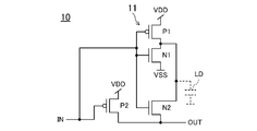
- FIG. 4 shows a first example of the circuit configuration of the delay circuit.
- the delay circuit 10 shown in FIG. 4 includes P-type transistors P1 and P2 and N-type transistors N1 and N2.
- the delay circuit 10 shown in FIG. 4 can measure the delay characteristic of the transistor N1 corresponding to the N-type transistor of the SRAM cell.
- the transistors P1 and N1 are connected in series between VDD as a high-voltage power supply and VSS as a low-voltage power supply, and their gates are connected to each other. That is, the transistors P1 and N1 form an inverter 11.
- FIG. Gates of the transistors P1 and N1 are connected to the input terminal IN.
- Transistors P1 and N1 correspond to transistors LD2 and DV2 in SRAM cell 20 shown in FIG. 2, respectively. That is, transistors P1 and N1 have the same size as transistors LD2 and DV2, respectively.
- the transistor P2 (pull-up transistor) has a gate connected to the input terminal IN, a source connected to VDD, and a drain connected to the output terminal OUT. When the input signal IN is low, the transistor P2 electrically connects VDD and the output terminal OUT.
- the transistor N2 (load separation transistor) has a gate connected to the input terminal IN and a drain connected to the output terminal OUT. Also, the source is connected to the drain of the transistor P1,N, that is, the output of the inverter 11. When the input signal IN is low, the transistor N2 electrically isolates the output of the inverter 11 from the output terminal OUT.
- a large load capacitance LD is provided at the output node of the inverter 11 .
- the load capacitance LD is implemented by wiring, capacitance, etc. so that the load is larger than the load capacitance connected to the output terminal OUT.
- the load capacitance LD is realized by a long wire, a dummy gate, or the like.
- the delay circuit 10 shown in FIG. 4 operates as follows. When signal IN transitions from low to high, transistor N2 turns on and the output of inverter 11 is electrically connected to output terminal OUT. Also, the transistor P2 is turned off. Then, the output signal OUT goes from high to low with a delay T_fN1 by turning on the transistor N1. Delay T_fN1 is the delay when the output of transistor N1 falls.
- the load capacitance LD is connected to the output terminal OUT when the signal IN transitions from low to high, but is not connected to the output terminal OUT when the signal IN transitions from high to low. Therefore, the relationship between delay T_fN1 and delay T_rP2 is T_fN1 > T_rP2 becomes.
- the ring oscillator 5 in FIG. 3 operates as follows when measuring the delay characteristics of the transistor N1. Make the enable signal EN high.
- the output of NAND circuit 15 transitions from high to low.
- the delay at this time is assumed to be T_fNAND.
- the first stage delay circuit 10 since the input IN transitioned from high to low, the output OUT transitions from low to high with a delay of T_rP2.
- the second stage delay circuit 10 since the input IN transitioned from low to high, the output OUT transitions from high to low with a delay of T_fN1. Since the third and subsequent delay circuits 10 perform similar operations, the output signal OUT transitions from high to low with a delay of N(T_fN1+T_rP2) in the 2N-stage delay circuits 10 as a whole.
- This output signal is fed back to the NAND circuit 15, and the output of the NAND circuit 15 transitions from low to high.
- the delay at this time be T_rNAND.
- the output OUT transitions from high to low with a delay of T_fN1.
- the output OUT transitions from low to high with a delay of T_rP2. Since the third and subsequent delay circuits 10 perform similar operations, the output signal OUT transitions from low to high with a delay of N(T_fN1+T_rP2) in the 2N stages of the delay circuits 10 as a whole.
- the ratio of the delay T_fN1 to the period T_cycle1 of the oscillation operation can be increased. Therefore, it is possible to improve the accuracy of the delay characteristic measurement of the transistor N1.
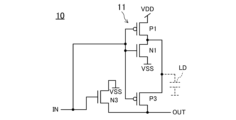
- FIG. 5 shows a second example of the circuit configuration of the delay circuit.
- the delay circuit 10 shown in FIG. 5 includes P-type transistors P1, P3 and N-type transistors N1, N3.
- the delay circuit 10 shown in FIG. 5 can measure the delay characteristic of the transistor P1 corresponding to the P-type transistor of the SRAM cell. Note that descriptions of components common to those in FIG. 4 may be omitted.
- the transistor N3 (pull-down transistor) has a gate connected to the input terminal IN, a source connected to VSS, and a drain connected to the output terminal OUT. When the input signal IN is high, the transistor N3 electrically connects VSS and the output terminal OUT.
- the transistor P3 (load isolation transistor) has a gate connected to the input terminal IN and a drain connected to the output terminal OUT. Also, the source is connected to the drains of the transistors P1 and N1, that is, the output of the inverter 11 . When the input signal IN is high, the transistor P3 electrically isolates the output of the inverter 11 from the output terminal OUT.
- the delay circuit 10 shown in FIG. 5 operates as follows. When signal IN transitions from high to low, transistor P3 turns on and the output of inverter 11 is electrically connected to output terminal OUT. Also, the transistor N3 is turned off. Then, the transistor P1 turns on, causing the output signal OUT to go from low to high with a delay T_rP1. Delay T_rP1 is the delay when the output of transistor P1 falls.
- T_fN3 is the delay when the output of transistor N3 falls.
- the load capacitance LD is connected to the output terminal OUT when the signal IN transitions from high to low, but is not connected to the output terminal OUT when the signal IN transitions from low to high. Therefore, the relationship between delay T_rP1 and delay T_fN3 is T_rP1 > T_fN3 becomes.
- the ring oscillator 5 in FIG. 3 operates as follows when measuring the delay characteristics of the transistor P1. Make the enable signal EN high.
- the output of NAND circuit 15 transitions from high to low with a delay of T_fNAND.
- the output OUT transitions from low to high with a delay of T_rP1.
- the output OUT transitions from high to low with a delay of T_fN3. Since the third and subsequent delay circuits 10 perform similar operations, the output signal OUT transitions from high to low with a delay of N(T_rP1+T_fN3) in the 2N-stage delay circuits 10 as a whole.
- This output signal is fed back to the NAND circuit 15, and the output of the NAND circuit 15 transitions from low to high with a delay of T_rNAND.
- the output OUT transitions from high to low with a delay of T_fN3.
- the output OUT transitions from low to high with a delay of T_rP1. Since the third and subsequent delay circuits 10 perform similar operations, the output signal OUT transitions from low to high with a delay of N(T_rP1+T_fN3) in the 2N-stage delay circuits 10 as a whole.
- T_cycle2 T_fNAND + T_rNAND + 2N (T_rP1 + T_fN3) becomes.
- the ratio of the delay T_rP1 to the period T_cycle2 of the oscillation operation can be increased. Therefore, it is possible to improve the accuracy of the delay characteristic measurement of the transistor P1.
- the semiconductor integrated circuit device 1 includes the ring oscillator 5 having the delay circuits 10 in multiple stages.
- each delay circuit 10 when the signal applied to the input terminal IN makes the first transition, the operation of the first transistor (N1 in FIG. 4, P1 in FIG. 5) corresponding to the transistor in the SRAM cell 20 causes , the signal at the output terminal OUT transitions.
- the signal applied to the input terminal IN makes the second transition, the first transistor corresponding to the transistor in the SRAM cell 20 is electrically isolated from the output terminal OUT, and the second transistor (see FIG. 4) is electrically separated from the output terminal OUT.
- the signal at the output terminal OUT transitions due to the operations of P2 and N3) in FIG.
- the ratio of the delay due to the first transistor to the oscillation period of the ring oscillator 5 can be increased. Therefore, it is possible to improve the accuracy of the delay characteristics of the first transistor.
- the first example and the second example described above may be implemented independently, respectively, or both may be implemented. That is, the semiconductor integrated circuit device according to the present disclosure may include a first ring oscillator having the delay circuit according to the first example and a second ring oscillator having the delay circuit according to the second example.
- the semiconductor integrated circuit device includes the SRAM circuit block, but the semiconductor integrated circuit device according to the present disclosure is not limited to this.
- a semiconductor integrated circuit device according to the present disclosure includes a logic circuit, and a characteristic measurement circuit for evaluating characteristics of transistors corresponding to transistors in the logic circuit includes a ring oscillator having the delay circuit described in the present disclosure. may be
Landscapes
- Engineering & Computer Science (AREA)
- Microelectronics & Electronic Packaging (AREA)
- Computer Hardware Design (AREA)
- Tests Of Electronic Circuits (AREA)
Priority Applications (3)
| Application Number | Priority Date | Filing Date | Title |
|---|---|---|---|
| JP2023543539A JP7709075B2 (ja) | 2021-08-25 | 2021-08-25 | 半導体集積回路装置 |
| PCT/JP2021/031085 WO2023026383A1 (ja) | 2021-08-25 | 2021-08-25 | 半導体集積回路装置 |
| US18/584,725 US12499963B2 (en) | 2021-08-25 | 2024-02-22 | Semiconductor integrated circuit device with a ring oscillator having a plurality of stages of delay circuits for measuring the delay characteristic of a transistor |
Applications Claiming Priority (1)
| Application Number | Priority Date | Filing Date | Title |
|---|---|---|---|
| PCT/JP2021/031085 WO2023026383A1 (ja) | 2021-08-25 | 2021-08-25 | 半導体集積回路装置 |
Related Child Applications (1)
| Application Number | Title | Priority Date | Filing Date |
|---|---|---|---|
| US18/584,725 Continuation US12499963B2 (en) | 2021-08-25 | 2024-02-22 | Semiconductor integrated circuit device with a ring oscillator having a plurality of stages of delay circuits for measuring the delay characteristic of a transistor |
Publications (1)
| Publication Number | Publication Date |
|---|---|
| WO2023026383A1 true WO2023026383A1 (ja) | 2023-03-02 |
Family
ID=85321906
Family Applications (1)
| Application Number | Title | Priority Date | Filing Date |
|---|---|---|---|
| PCT/JP2021/031085 Ceased WO2023026383A1 (ja) | 2021-08-25 | 2021-08-25 | 半導体集積回路装置 |
Country Status (3)
| Country | Link |
|---|---|
| US (1) | US12499963B2 (https=) |
| JP (1) | JP7709075B2 (https=) |
| WO (1) | WO2023026383A1 (https=) |
Families Citing this family (1)
| Publication number | Priority date | Publication date | Assignee | Title |
|---|---|---|---|---|
| US20240162895A1 (en) * | 2022-11-16 | 2024-05-16 | International Business Machines Corporation | Competing path ring-oscillator for direct measurement of a latch timing window parameters |
Citations (2)
| Publication number | Priority date | Publication date | Assignee | Title |
|---|---|---|---|---|
| JP2014010874A (ja) * | 2012-07-02 | 2014-01-20 | Fujitsu Semiconductor Ltd | リング発振器及び半導体装置 |
| JP2014150353A (ja) * | 2013-01-31 | 2014-08-21 | Fujitsu Semiconductor Ltd | リング発振器及び半導体装置 |
Family Cites Families (8)
| Publication number | Priority date | Publication date | Assignee | Title |
|---|---|---|---|---|
| JP2748865B2 (ja) * | 1994-09-27 | 1998-05-13 | 日本電気株式会社 | 出力回路 |
| JP2001101870A (ja) * | 1999-09-30 | 2001-04-13 | Fujitsu Ltd | 半導体集積回路 |
| JP2002009601A (ja) * | 2000-06-27 | 2002-01-11 | Fujitsu Ltd | 半導体集積回路および半導体集積回路の初期化方法 |
| JP3939208B2 (ja) * | 2002-06-24 | 2007-07-04 | 富士通株式会社 | 出力パルスサイクルを短くできるパルス発生回路 |
| JP2008219232A (ja) * | 2007-03-01 | 2008-09-18 | Matsushita Electric Ind Co Ltd | 半導体集積回路 |
| JP5200506B2 (ja) * | 2007-11-28 | 2013-06-05 | 富士通セミコンダクター株式会社 | メモリ装置 |
| JP2010073282A (ja) * | 2008-09-19 | 2010-04-02 | Nec Electronics Corp | 半導体装置、半導体装置の設計方法 |
| US10964379B2 (en) * | 2018-11-07 | 2021-03-30 | Arm Limited | Ring oscillator based bitcell delay monitor |
-
2021
- 2021-08-25 WO PCT/JP2021/031085 patent/WO2023026383A1/ja not_active Ceased
- 2021-08-25 JP JP2023543539A patent/JP7709075B2/ja active Active
-
2024
- 2024-02-22 US US18/584,725 patent/US12499963B2/en active Active
Patent Citations (2)
| Publication number | Priority date | Publication date | Assignee | Title |
|---|---|---|---|---|
| JP2014010874A (ja) * | 2012-07-02 | 2014-01-20 | Fujitsu Semiconductor Ltd | リング発振器及び半導体装置 |
| JP2014150353A (ja) * | 2013-01-31 | 2014-08-21 | Fujitsu Semiconductor Ltd | リング発振器及び半導体装置 |
Also Published As
| Publication number | Publication date |
|---|---|
| JPWO2023026383A1 (https=) | 2023-03-02 |
| US20240233854A1 (en) | 2024-07-11 |
| US12499963B2 (en) | 2025-12-16 |
| JP7709075B2 (ja) | 2025-07-16 |
Similar Documents
| Publication | Publication Date | Title |
|---|---|---|
| US8183639B2 (en) | Dual port static random access memory cell layout | |
| JP5624441B2 (ja) | 半導体装置 | |
| KR101914690B1 (ko) | 네가티브 바이어스 온도 불안정에 견디는 래칭 센스 증폭기를 갖는 메모리 및 그 방법 | |
| US7479818B2 (en) | Sense amplifier flip flop | |
| KR100516226B1 (ko) | 에스램 테스트용 셀 및 에스램 셀 테스트 방법 | |
| US10529388B2 (en) | Current-mode sense amplifier | |
| JP6504734B2 (ja) | リレーデバイスを有するメモリ要素 | |
| TW201340609A (zh) | 位準移位電路以及利用位準移位電路之半導體裝置 | |
| CN108122580A (zh) | 存储单元及其工作方法 | |
| CN111899776A (zh) | 一种降低静态随机存储器中灵敏放大器失调电压的电路结构 | |
| US8693264B2 (en) | Memory device having sensing circuitry with automatic latching of sense amplifier output node | |
| JP3144395B2 (ja) | ディレイ回路 | |
| US20040140835A1 (en) | Multiple trip point fuse latch device and method | |
| JP7709075B2 (ja) | 半導体集積回路装置 | |
| US7030643B2 (en) | Output buffer circuits including logic gates having balanced output nodes | |
| Kishor et al. | Design of a ternary FinFET SRAM cell | |
| TWI862573B (zh) | 電壓位準偏移設備及其操作方法 | |
| US6384658B1 (en) | Clock splitter circuit to generate synchronized clock and inverted clock | |
| JP3161598B2 (ja) | 半導体集積回路およびその製造方法 | |
| CN113793630B (zh) | 一种标准单元的传输延迟确定方法及装置 | |
| US20130235681A1 (en) | Implementing rc and coupling delay correction for sram | |
| JPH05199101A (ja) | レベルシフト回路 | |
| CN108564979B (zh) | 单端读取电路 | |
| TW201304075A (zh) | 半導體裝置及製作方法 | |
| CN111865291B (zh) | 一种抗双节点翻转的锁存器 |
Legal Events
| Date | Code | Title | Description |
|---|---|---|---|
| 121 | Ep: the epo has been informed by wipo that ep was designated in this application |
Ref document number: 21954997 Country of ref document: EP Kind code of ref document: A1 |
|
| WWE | Wipo information: entry into national phase |
Ref document number: 2023543539 Country of ref document: JP |
|
| NENP | Non-entry into the national phase |
Ref country code: DE |
|
| 122 | Ep: pct application non-entry in european phase |
Ref document number: 21954997 Country of ref document: EP Kind code of ref document: A1 |