WO2023013742A1 - 弾性波装置 - Google Patents
弾性波装置 Download PDFInfo
- Publication number
- WO2023013742A1 WO2023013742A1 PCT/JP2022/030014 JP2022030014W WO2023013742A1 WO 2023013742 A1 WO2023013742 A1 WO 2023013742A1 JP 2022030014 W JP2022030014 W JP 2022030014W WO 2023013742 A1 WO2023013742 A1 WO 2023013742A1
- Authority
- WO
- WIPO (PCT)
- Prior art keywords
- electrode
- wave device
- electrode fingers
- piezoelectric layer
- elastic wave
- Prior art date
- Legal status (The legal status is an assumption and is not a legal conclusion. Google has not performed a legal analysis and makes no representation as to the accuracy of the status listed.)
- Ceased
Links
Images












Classifications
-
- H—ELECTRICITY
- H03—ELECTRONIC CIRCUITRY
- H03H—IMPEDANCE NETWORKS, e.g. RESONANT CIRCUITS; RESONATORS
- H03H9/00—Networks comprising electromechanical or electro-acoustic elements; Electromechanical resonators
- H03H9/02—Details
- H03H9/02228—Guided bulk acoustic wave devices or Lamb wave devices having interdigital transducers situated in parallel planes on either side of a piezoelectric layer
-
- H—ELECTRICITY
- H03—ELECTRONIC CIRCUITRY
- H03H—IMPEDANCE NETWORKS, e.g. RESONANT CIRCUITS; RESONATORS
- H03H9/00—Networks comprising electromechanical or electro-acoustic elements; Electromechanical resonators
- H03H9/02—Details
- H03H9/02007—Details of bulk acoustic wave devices
- H03H9/02086—Means for compensation or elimination of undesirable effects
-
- H—ELECTRICITY
- H03—ELECTRONIC CIRCUITRY
- H03H—IMPEDANCE NETWORKS, e.g. RESONANT CIRCUITS; RESONATORS
- H03H9/00—Networks comprising electromechanical or electro-acoustic elements; Electromechanical resonators
- H03H9/02—Details
- H03H9/02007—Details of bulk acoustic wave devices
- H03H9/02015—Characteristics of piezoelectric layers, e.g. cutting angles
-
- H—ELECTRICITY
- H03—ELECTRONIC CIRCUITRY
- H03H—IMPEDANCE NETWORKS, e.g. RESONANT CIRCUITS; RESONATORS
- H03H9/00—Networks comprising electromechanical or electro-acoustic elements; Electromechanical resonators
- H03H9/02—Details
- H03H9/02007—Details of bulk acoustic wave devices
- H03H9/02015—Characteristics of piezoelectric layers, e.g. cutting angles
- H03H9/02031—Characteristics of piezoelectric layers, e.g. cutting angles consisting of ceramic
-
- H—ELECTRICITY
- H03—ELECTRONIC CIRCUITRY
- H03H—IMPEDANCE NETWORKS, e.g. RESONANT CIRCUITS; RESONATORS
- H03H9/00—Networks comprising electromechanical or electro-acoustic elements; Electromechanical resonators
- H03H9/02—Details
- H03H9/125—Driving means, e.g. electrodes, coils
- H03H9/13—Driving means, e.g. electrodes, coils for networks consisting of piezoelectric or electrostrictive materials
-
- H—ELECTRICITY
- H03—ELECTRONIC CIRCUITRY
- H03H—IMPEDANCE NETWORKS, e.g. RESONANT CIRCUITS; RESONATORS
- H03H9/00—Networks comprising electromechanical or electro-acoustic elements; Electromechanical resonators
- H03H9/15—Constructional features of resonators consisting of piezoelectric or electrostrictive material
- H03H9/17—Constructional features of resonators consisting of piezoelectric or electrostrictive material having a single resonator
- H03H9/171—Constructional features of resonators consisting of piezoelectric or electrostrictive material having a single resonator implemented with thin-film techniques, i.e. of the film bulk acoustic resonator [FBAR] type
- H03H9/172—Means for mounting on a substrate, i.e. means constituting the material interface confining the waves to a volume
- H03H9/173—Air-gaps
Definitions
- the present disclosure relates to elastic wave devices.
- Patent Document 1 describes an elastic wave device.
- leakage of elastic waves may occur in the direction in which the electrode fingers extend.
- the present disclosure is intended to solve the above-described problems, and aims to suppress leakage of elastic waves.
- An elastic wave device includes a support member including a support substrate having a thickness in a first direction, a piezoelectric layer provided in the first direction of the support member, a main surface of the piezoelectric layer provided, a plurality of first electrode fingers extending in a second direction intersecting the first direction; a first busbar electrode to which the plurality of first electrode fingers are connected; an IDT electrode having a plurality of second electrode fingers facing any one of the plurality of first electrode fingers and extending in the second direction; and a second busbar electrode to which the plurality of second electrode fingers are connected;
- the piezoelectric layer is positioned between at least one first electrode finger and the second busbar electrode or between at least one second electrode finger and the first busbar electrode and a piezoelectric laminate structure including a first piezoelectric body and a second piezoelectric body having a different dielectric polarization state from the first piezoelectric body in a gap region between.
- elastic wave leakage can be suppressed.
- FIG. 1A is a perspective view showing an elastic wave device according to a first embodiment
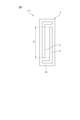
- FIG. 1B is a plan view showing the electrode structure of the first embodiment.
- FIG. 2 is a cross-sectional view of a portion along line II-II of FIG. 1A.
- FIG. 3A is a schematic cross-sectional view for explaining Lamb waves propagating through the piezoelectric layer of the comparative example.
- FIG. 3B is a schematic cross-sectional view for explaining a thickness-shear primary mode bulk wave propagating through the piezoelectric layer of the first embodiment.
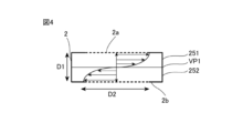
- FIG. 4 is a schematic cross-sectional view for explaining the amplitude direction of a thickness-shear primary mode bulk wave propagating in the piezoelectric layer of the first embodiment.
- FIG. 1A is a perspective view showing an elastic wave device according to a first embodiment
- FIG. 1B is a plan view showing the electrode structure of the first embodiment.
- FIG. 2 is a cross-sectional view of a portion along line II
- FIG. 5 is an explanatory diagram showing an example of resonance characteristics of the elastic wave device of the first embodiment.
- FIG. 2 is an explanatory diagram showing the relationship between , and the fractional band.
- FIG. FIG. 7 is a plan view showing an example in which a pair of electrodes are provided in the elastic wave device of the first embodiment.
- FIG. 8 is a reference diagram showing an example of resonance characteristics of the elastic wave device of the first embodiment.
- FIG. 9 shows the ratio bandwidth when a large number of elastic wave resonators are configured in the elastic wave device of the first embodiment, and the phase rotation amount of the spurious impedance normalized by 180 degrees as the magnitude of the spurious. is an explanatory diagram showing the relationship between.
- FIG. 9 shows the ratio bandwidth when a large number of elastic wave resonators are configured in the elastic wave device of the first embodiment, and the phase rotation amount of the spurious impedance normalized by 180 degrees as the magnitude of the spurious.
- FIG. 10 is an explanatory diagram showing the relationship between d/2p, metallization ratio MR, and fractional bandwidth.
- FIG. 11 is an explanatory diagram showing a map of the fractional band with respect to the Euler angles (0°, ⁇ , ⁇ ) of LiNbO 3 when d/p is infinitely close to 0.
- FIG. 12 is a modification of the first embodiment, and is a cross-sectional view of a portion taken along line II-II of FIG. 1A.
- FIG. 13 is a partially cutaway perspective view for explaining the elastic wave device according to the embodiment of the present disclosure.
- 14 is a plan view showing an example of the elastic wave device according to the first embodiment;
- FIG. 15 is a cross-sectional view taken along line XV-XV of FIG. 14.
- FIG. 16 is a cross-sectional view showing a first modification of the elastic wave device according to the first embodiment.
- FIG. 17 is a plan view showing a second modification of the elastic wave device according to the first embodiment;
- FIG. 18 is an explanatory diagram showing an example of admittance characteristics of the elastic wave device according to the first embodiment.
- FIG. 19 is an explanatory diagram showing an example of admittance characteristics of the elastic wave device according to the first embodiment.
- FIG. 20 is a plan view showing an example of the elastic wave device according to the second embodiment. 21 is a cross-sectional view taken along line XXI-XXI of FIG. 20.
- FIG. 1A is a perspective view showing an elastic wave device according to a first embodiment
- FIG. 1B is a plan view showing the electrode structure of the first embodiment.
- the elastic wave device 1 of the first embodiment has a piezoelectric layer 2 made of LiNbO 3 .
- the piezoelectric layer 2 may consist of LiTaO 3 .
- the cut angle of LiNbO 3 and LiTaO 3 is Z-cut in the first embodiment.
- the cut angles of LiNbO 3 and LiTaO 3 may be rotated Y-cut or X-cut.
- the Y-propagation and X-propagation ⁇ 30° propagation orientations are preferred.
- the thickness of the piezoelectric layer 2 is not particularly limited, it is preferably 50 nm or more and 1000 nm or less in order to effectively excite the thickness shear primary mode.
- the piezoelectric layer 2 has a first main surface 2a and a second main surface 2b facing each other in the Z direction. Electrode fingers 3 and 4 are provided on the first main surface 2a.
- the electrode finger 3 is an example of the "first electrode finger” and the electrode finger 4 is an example of the "second electrode finger”.
- the multiple electrode fingers 3 are multiple “first electrodes” connected to the first busbar electrodes 5 .
- a plurality of electrode fingers 4 are a plurality of “second electrodes” connected to second busbar electrodes 6 .
- the plurality of electrode fingers 3 and the plurality of electrode fingers 4 are interdigitated with each other.
- an IDT (Interdigital Transducer) electrode including electrode fingers 3 , electrode fingers 4 , first busbar electrodes 5 , and second busbar electrodes 6 is configured.
- the electrode fingers 3 and 4 have a rectangular shape and a length direction.
- the electrode finger 3 and the electrode finger 4 adjacent to the electrode finger 3 face each other in a direction perpendicular to the length direction.
- Both the length direction of the electrode fingers 3 and 4 and the direction orthogonal to the length direction of the electrode fingers 3 and 4 are directions that intersect the thickness direction of the piezoelectric layer 2 . Therefore, it can be said that the electrode finger 3 and the electrode finger 4 adjacent to the electrode finger 3 face each other in the direction intersecting the thickness direction of the piezoelectric layer 2 .
- the thickness direction of the piezoelectric layer 2 is defined as the Z direction (or first direction)
- the length direction of the electrode fingers 3 and 4 is defined as the Y direction (or second direction)
- the electrode fingers 3 and electrode fingers 4 may be described as the X direction (or the third direction).
- the length direction of the electrode fingers 3 and 4 may be interchanged with the direction orthogonal to the length direction of the electrode fingers 3 and 4 shown in FIGS. 1A and 1B. That is, in FIGS. 1A and 1B, the electrode fingers 3 and 4 may extend in the direction in which the first busbar electrodes 5 and the second busbar electrodes 6 extend. In that case, the first busbar electrode 5 and the second busbar electrode 6 extend in the direction in which the electrode fingers 3 and 4 extend in FIGS. 1A and 1B.
- a pair of structures in which the electrode fingers 3 connected to one potential and the electrode fingers 4 connected to the other potential are adjacent to each other are arranged in a direction perpendicular to the length direction of the electrode fingers 3 and 4. Multiple pairs are provided.
- the electrode finger 3 and the electrode finger 4 are adjacent to each other, not when the electrode finger 3 and the electrode finger 4 are arranged so as to be in direct contact, but when the electrode finger 3 and the electrode finger 4 are arranged with a gap therebetween. It refers to the case where the When the electrode finger 3 and the electrode finger 4 are adjacent to each other, there are electrodes connected to the hot electrode and the ground electrode, including other electrode fingers 3 and 4, between the electrode finger 3 and the electrode finger 4. is not placed.
- the logarithms need not be integer pairs, but may be 1.5 pairs, 2.5 pairs, or the like.
- the center-to-center distance, that is, the pitch, between the electrode fingers 3 and 4 is preferably in the range of 1 ⁇ m or more and 10 ⁇ m or less. Further, the center-to-center distance between the electrode fingers 3 and 4 means the center of the width dimension of the electrode fingers 3 in the direction orthogonal to the length direction of the electrode fingers 3 and the distance orthogonal to the length direction of the electrode fingers 4 . It is the distance connecting the center of the width dimension of the electrode finger 4 in the direction of
- the electrode fingers 3 and 4 when at least one of the electrode fingers 3 and 4 is plural (when there are 1.5 or more pairs of electrodes when the electrode fingers 3 and 4 are paired as a pair of electrode pairs), the electrode fingers 3.
- the center-to-center distance of the electrode fingers 4 refers to the average value of the center-to-center distances of adjacent electrode fingers 3 and electrode fingers 4 among 1.5 or more pairs of electrode fingers 3 and electrode fingers 4 .
- the width of the electrode fingers 3 and 4 that is, the dimension in the facing direction of the electrode fingers 3 and 4 is preferably in the range of 150 nm or more and 1000 nm or less.
- the center-to-center distance between the electrode fingers 3 and 4 is the distance between the center of the dimension (width dimension) of the electrode finger 3 in the direction perpendicular to the length direction of the electrode finger 3 and the length of the electrode finger 4. It is the distance connecting the center of the dimension (width dimension) of the electrode finger 4 in the direction orthogonal to the direction.
- the direction orthogonal to the length direction of the electrode fingers 3 and 4 is the direction orthogonal to the polarization direction of the piezoelectric layer 2 .
- “perpendicular” is not limited to being strictly perpendicular, but substantially perpendicular (the angle formed by the direction perpendicular to the length direction of the electrode fingers 3 and electrode fingers 4 and the polarization direction is, for example, 90° ⁇ 10°).
- a support substrate 8 is laminated on the second main surface 2b side of the piezoelectric layer 2 with an intermediate layer 7 interposed therebetween.
- the intermediate layer 7 and the support substrate 8 have a frame shape and, as shown in FIG. 2, openings 7a and 8a.
- a space (air gap) 9 is thereby formed.
- the space 9 is provided so as not to disturb the vibration of the excitation region C of the piezoelectric layer 2 . Therefore, the support substrate 8 is laminated on the second main surface 2b with the intermediate layer 7 interposed therebetween at a position not overlapping the portion where at least one pair of electrode fingers 3 and 4 are provided. Note that the intermediate layer 7 may not be provided. Therefore, the support substrate 8 can be directly or indirectly laminated to the second main surface 2b of the piezoelectric layer 2 .
- the intermediate layer 7 is made of silicon oxide.
- the intermediate layer 7 can be formed of an appropriate insulating material other than silicon oxide, such as silicon nitride and alumina.
- the support substrate 8 is made of Si.
- the plane orientation of the surface of Si on the piezoelectric layer 2 side may be (100), (110), or (111).
- high-resistance Si having a resistivity of 4 k ⁇ or more is desirable.
- the support substrate 8 can also be constructed using an appropriate insulating material or semiconductor material.
- Materials for the support substrate 8 include, for example, aluminum oxide, lithium tantalate, lithium niobate, piezoelectric materials such as crystal, alumina, magnesia, sapphire, silicon nitride, aluminum nitride, silicon carbide, zirconia, cordierite, mullite, and steer.
- Various ceramics such as tight and forsterite, dielectrics such as diamond and glass, and semiconductors such as gallium nitride can be used.
- the plurality of electrode fingers 3, electrode fingers 4, first busbar electrodes 5, and second busbar electrodes 6 are made of appropriate metals or alloys such as Al and AlCu alloys.
- the electrode fingers 3, the electrode fingers 4, the first busbar electrodes 5, and the second busbar electrodes 6 have a structure in which an Al film is laminated on a Ti film. Note that an adhesion layer other than the Ti film may be used.
- an AC voltage is applied between the multiple electrode fingers 3 and the multiple electrode fingers 4 . More specifically, an AC voltage is applied between the first busbar electrode 5 and the second busbar electrode 6 . As a result, it is possible to obtain resonance characteristics using a thickness-shear primary mode bulk wave excited in the piezoelectric layer 2 .
- d/p is set to 0.5 or less.
- the thickness-shear primary mode bulk wave is effectively excited, and good resonance characteristics can be obtained. More preferably, d/p is 0.24 or less, in which case even better resonance characteristics can be obtained.
- the electrode fingers 3 and the electrode fingers 4 When at least one of the electrode fingers 3 and the electrode fingers 4 is plural as in the first embodiment, that is, when the electrode fingers 3 and the electrode fingers 4 form a pair of electrodes, the electrode fingers 3 and the electrode fingers When there are 1.5 pairs or more of 4, the center-to-center distance p between the adjacent electrode fingers 3 and 4 is the average distance between the center-to-center distances between the adjacent electrode fingers 3 and 4 .
- the acoustic wave device 1 of the first embodiment has the above configuration, even if the logarithms of the electrode fingers 3 and 4 are reduced in an attempt to reduce the size, the Q value is unlikely to decrease. This is because the resonator does not require reflectors on both sides, and the propagation loss is small. The reason why the above reflector is not required is that the bulk wave of the thickness-shlip primary mode is used.
- FIG. 3A is a schematic cross-sectional view for explaining Lamb waves propagating through the piezoelectric layer of the comparative example.
- FIG. 3B is a schematic cross-sectional view for explaining a thickness-shear primary mode bulk wave propagating through the piezoelectric layer of the first embodiment.
- FIG. 4 is a schematic cross-sectional view for explaining the amplitude direction of a thickness-shear primary mode bulk wave propagating in the piezoelectric layer of the first embodiment.
- FIG. 3A shows an acoustic wave device as described in Patent Document 1, in which Lamb waves propagate through the piezoelectric layer.
- waves propagate through the piezoelectric layer 201 as indicated by arrows.
- the piezoelectric layer 201 has a first principal surface 201a and a second principal surface 201b, and the thickness direction connecting the first principal surface 201a and the second principal surface 201b is the Z direction.
- the X direction is the direction in which the electrode fingers 3 and 4 of the IDT electrodes are aligned.
- the Lamb wave the wave propagates in the X direction as shown.
- the wave is applied to the first main surface 2a and the second main surface 2b of the piezoelectric layer 2. , that is, in the Z direction, and resonate. That is, the X-direction component of the wave is significantly smaller than the Z-direction component. Further, since resonance characteristics are obtained by propagating waves in the Z direction, no reflector is required. Therefore, no propagation loss occurs when propagating to the reflector. Therefore, even if the number of electrode pairs consisting of the electrode fingers 3 and 4 is reduced in an attempt to promote miniaturization, the Q value is unlikely to decrease.
- the amplitude direction of the bulk wave of the primary thickness-shear mode is the first region 251 included in the excitation region C (see FIG. 1B) of the piezoelectric layer 2 and the first region 251 included in the excitation region C (see FIG. 1B). 2 area 252 is reversed.
- FIG. 4 schematically shows bulk waves when a voltage is applied between the electrode fingers 3 so that the electrode fingers 4 have a higher potential than the electrode fingers 3 .
- the first region 251 is a region of the excitation region C between the virtual plane VP1 that is orthogonal to the thickness direction of the piezoelectric layer 2 and bisects the piezoelectric layer 2 and the first main surface 2a.
- the second region 252 is a region of the excitation region C between the virtual plane VP1 and the second main surface 2b.
- At least one pair of electrodes consisting of the electrode fingers 3 and 4 is arranged. It is not always necessary to have a plurality of pairs of electrode pairs. That is, it is sufficient that at least one pair of electrodes is provided.
- the electrode finger 3 is an electrode connected to a hot potential
- the electrode finger 4 is an electrode connected to a ground potential.
- the electrode finger 3 may be connected to the ground potential and the electrode finger 4 to the hot potential.
- the at least one pair of electrodes are, as described above, electrodes connected to a hot potential or electrodes connected to a ground potential, and no floating electrodes are provided.
- FIG. 5 is an explanatory diagram showing an example of resonance characteristics of the elastic wave device of the first embodiment.
- the design parameters of the acoustic wave device 1 that obtained the resonance characteristics shown in FIG. 5 are as follows.
- Piezoelectric layer 2 LiNbO3 with Euler angles (0°, 0°, 90°) Thickness of piezoelectric layer 2: 400 nm
- Length of excitation region C (see FIG. 1B): 40 ⁇ m Number of electrode pairs consisting of electrode fingers 3 and 4: 21 pairs Center-to-center distance (pitch) between electrode fingers 3 and 4: 3 ⁇ m Width of electrode fingers 3 and 4: 500 nm d/p: 0.133
- Middle layer 7 Silicon oxide film with a thickness of 1 ⁇ m
- Support substrate 8 Si
- the excitation region C (see FIG. 1B) is a region where the electrode fingers 3 and 4 overlap when viewed in the X direction perpendicular to the length direction of the electrode fingers 3 and 4. .
- the length of the excitation region C is the dimension along the length direction of the electrode fingers 3 and 4 of the excitation region C. As shown in FIG. Here, the excitation region C is an example of the "intersection region".
- the inter-electrode distances of the electrode pairs consisting of the electrode fingers 3 and 4 are all equal in a plurality of pairs. That is, the electrode fingers 3 and the electrode fingers 4 are arranged at equal pitches.
- d/p is 0.5 or less, more preferably 0. .24 or less. This will be explained with reference to FIG.
- FIG. 6 shows d/2p, where p is the center-to-center distance between adjacent electrodes or the average distance of the center-to-center distances, and d is the average thickness of the piezoelectric layer 2. It is an explanatory view showing the relationship with the fractional bandwidth as.
- At least one pair of electrodes may be one pair, and the above p is the center-to-center distance between adjacent electrode fingers 3 and 4 in the case of one pair of electrodes. In the case of 1.5 pairs or more of electrodes, the average distance between the centers of adjacent electrode fingers 3 and 4 should be p.
- the thickness d of the piezoelectric layer 2 if the piezoelectric layer 2 has variations in thickness, a value obtained by averaging the thickness may be adopted.
- FIG. 7 is a plan view showing an example in which a pair of electrodes are provided in the elastic wave device of the first embodiment.
- a pair of electrodes having electrode fingers 3 and 4 are provided on first main surface 2 a of piezoelectric layer 2 .
- K in FIG. 7 is the intersection width.
- the number of pairs of electrodes may be one. Even in this case, if the above d/p is 0.5 or less, it is possible to effectively excite the bulk wave in the primary mode of thickness shear.
- the excitation region is an overlapping region of the plurality of electrode fingers 3 and 4 when viewed in the direction in which any adjacent electrode fingers 3 and 4 are facing each other. It is desirable that the metallization ratio MR of the adjacent electrode fingers 3 and 4 with respect to the region C satisfies MR ⁇ 1.75(d/p)+0.075. In that case, spurious can be effectively reduced. This will be described with reference to FIGS. 8 and 9. FIG.
- FIG. 8 is a reference diagram showing an example of resonance characteristics of the elastic wave device of the first embodiment.
- a spurious signal indicated by an arrow B appears between the resonance frequency and the anti-resonance frequency.
- d/p 0.08 and the Euler angles of LiNbO 3 (0°, 0°, 90°).
- the metallization ratio MR was set to 0.35.
- the metallization ratio MR will be explained with reference to FIG. 1B.
- the excitation region C is the portion surrounded by the dashed-dotted line.
- the excitation region C is a region where the electrode fingers 3 and 4 overlap with the electrode fingers 4 when viewed in a direction perpendicular to the length direction of the electrode fingers 3 and 4, that is, in a facing direction. a region where the electrode fingers 3 overlap each other; and a region between the electrode fingers 3 and 4 where the electrode fingers 3 and 4 overlap each other.
- the area of the electrode fingers 3 and 4 in the excitation region C with respect to the area of the excitation region C is the metallization ratio MR. That is, the metallization ratio MR is the ratio of the area of the metallization portion to the area of the excitation region C.
- the ratio of the metallization portion included in the entire excitation region C to the total area of the excitation region C should be MR.
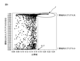
- FIG. 9 shows the ratio bandwidth when a large number of elastic wave resonators are configured in the elastic wave device of the first embodiment, and the phase rotation amount of the spurious impedance normalized by 180 degrees as the magnitude of the spurious. is an explanatory diagram showing the relationship between. The ratio band was adjusted by changing the film thickness of the piezoelectric layer 2 and the dimensions of the electrode fingers 3 and 4 .
- FIG. 9 shows the results when the piezoelectric layer 2 made of Z-cut LiNbO 3 is used, but the same tendency is obtained when the piezoelectric layer 2 with other cut angles is used.
- the spurious is as large as 1.0.
- the fractional band exceeds 0.17, that is, exceeds 17%, a large spurious with a spurious level of 1 or more changes the parameters constituting the fractional band, even if the passband appear within. That is, as in the resonance characteristics shown in FIG. 8, a large spurious component indicated by arrow B appears within the band. Therefore, the specific bandwidth is preferably 17% or less. In this case, by adjusting the film thickness of the piezoelectric layer 2 and the dimensions of the electrode fingers 3 and 4, the spurious response can be reduced.
- FIG. 10 is an explanatory diagram showing the relationship between d/2p, metallization ratio MR, and fractional bandwidth.
- various elastic wave devices 1 with different d/2p and MR were configured, and the fractional bandwidth was measured.
- the hatched portion on the right side of the dashed line D in FIG. 10 is the area where the fractional bandwidth is 17% or less.
- FIG. 11 is an explanatory diagram showing a map of the fractional band with respect to the Euler angles (0°, ⁇ , ⁇ ) of LiNbO 3 when d/p is infinitely close to 0.
- FIG. A hatched portion in FIG. 11 is a region where a fractional bandwidth of at least 5% or more is obtained. When the range of the area is approximated, it becomes the range represented by the following formulas (1), (2) and (3).
- Equation (1) (0° ⁇ 10°, 20° to 80°, 0° to 60° (1-( ⁇ -50) 2 /900) 1/2 ) or (0° ⁇ 10°, 20° to 80°, [180 °-60° (1-( ⁇ -50) 2 /900) 1/2 ] ⁇ 180°) Equation (2) (0° ⁇ 10°, [180°-30°(1-( ⁇ -90) 2 /8100) 1/2 ] ⁇ 180°, arbitrary ⁇ ) Equation (3)
- the fractional band can be sufficiently widened, which is preferable.
- FIG. 12 is a modification of the first embodiment, and is a cross-sectional view of a portion taken along line II-II of FIG. 1A.
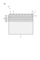
- an acoustic multilayer film 42 is laminated on the second main surface 2 b of the piezoelectric layer 2 .
- the acoustic multilayer film 42 has a laminated structure of low acoustic impedance layers 42a, 42c, 42e with relatively low acoustic impedance and high acoustic impedance layers 42b, 42d with relatively high acoustic impedance.
- the low acoustic impedance layer is, for example, a layer of SiO2
- the high acoustic impedance layer is, for example, a metal layer such as W, Pt or a dielectric layer such as AlN, SiN.
- the thickness-shear primary mode bulk wave can be confined in the piezoelectric layer 2 without using the space 9 in the elastic wave device 1 .
- the acoustic wave device 41 by setting the above d/p to 0.5 or less, it is possible to obtain resonance characteristics based on bulk waves in the first-order thickness shear mode.
- the number of lamination of the low acoustic impedance layers 42a, 42c, 42e and the high acoustic impedance layers 42b, 42d is not particularly limited. At least one of the high acoustic impedance layers 42b, 42d needs to be arranged farther from the piezoelectric layer 2 than the low acoustic impedance layers 42a, 42c, 42e.
- the low acoustic impedance layers 42a, 42c, 42e and the high acoustic impedance layers 42b, 42d can be made of appropriate materials as long as the acoustic impedance relationship is satisfied.
- Examples of materials for the low acoustic impedance layers 42a, 42c, and 42e include silicon oxide and silicon oxynitride.
- Materials for the high acoustic impedance layers 42b and 42d include alumina, silicon nitride, and metals.
- FIG. 13 is a partially cutaway perspective view for explaining the elastic wave device according to the embodiment of the present disclosure.
- the outer peripheral edge of the space portion 9 is indicated by a dashed line.
- the elastic wave device of the present disclosure may utilize plate waves.
- the elastic wave device 301 has reflectors 310 and 311 as shown in FIG. Reflectors 310 and 311 are provided on both sides of the electrode fingers 3 and 4 of the piezoelectric layer 2 in the acoustic wave propagation direction.
- a Lamb wave as a plate wave is excited by applying an AC electric field to the electrode fingers 3 and 4 on the space 9.
- the reflectors 310 and 311 are provided on both sides, it is possible to obtain resonance characteristics due to Lamb waves as Lamb waves.
- the elastic wave devices 1 and 101 use bulk waves in the primary mode of thickness shear.
- the first electrode finger 3 and the second electrode finger 4 are adjacent electrodes, the thickness of the piezoelectric layer 2 is d, and the center of the first electrode finger 3 and the second electrode finger 4 is d/p is set to 0.5 or less, where p is the distance between them.
- the Q value can be increased even if the elastic wave device is miniaturized.
- the piezoelectric layer 2 is made of lithium niobate or lithium tantalate.
- the first principal surface 2a or the second principal surface 2b of the piezoelectric layer 2 has a first electrode finger 3 and a second electrode finger 4 facing each other in a direction intersecting the thickness direction of the piezoelectric layer 2. and the second electrode fingers 4 are desirably covered with a protective film.
- FIG. 14 is a plan view showing an example of the elastic wave device according to the first embodiment.
- 15 is a cross-sectional view taken along line XV-XV of FIG. 14.
- FIG. An acoustic wave device 1A according to the first embodiment includes a piezoelectric layer 2, IDT electrodes including electrode fingers 3 and 4 and busbar electrodes 5 and 6, and a support member.
- IDT electrodes including electrode fingers 3 and 4 and busbar electrodes 5 and 6, and a support member.
- the direction from the second main surface 2b of the piezoelectric layer 2 to the first main surface 2a is the top
- the direction from the first main surface 2a to the second main surface of the piezoelectric layer 2 is the top.
- the direction toward 2b may be described as the bottom.
- the support member is a member provided with the support substrate 8 .
- the support member consists of a support substrate 8 .
- the piezoelectric layer 2 is provided on the support substrate 8 in the Z direction.
- the support member may further include an intermediate layer 7 provided in the Z direction of the support substrate 8 .
- the support member has a space portion 9 at a position at least partially overlapping with the IDT electrode when viewed from above in the Z direction.
- the space 9 is provided so as to penetrate the support substrate 8 in the Z direction, but this is only an example, and may be provided only on the piezoelectric layer 2 side of the support member.
- the piezoelectric layer 2 is provided in the Z direction of the support member.
- the piezoelectric layer 2 is a layer containing piezoelectric lithium niobate and unavoidable impurities, and is, for example, single crystal Z-cut lithium niobate.
- the direction of dielectric polarization in the intersection region C of the piezoelectric layer 2 is upward.
- the direction of dielectric polarization refers to the direction of the polarization vector generated by dielectric polarization.
- the first main surface 2a of the piezoelectric layer 2 is a surface having a positive potential (dielectric positive potential surface) due to dielectric polarization, and the second main surface 2b has a negative potential due to dielectric polarization. (dielectric negative potential surface).
- the present inventors have found that in an elastic wave device that utilizes a thickness-shear first-order bulk elastic wave, an elastic wave leakage mode is generated outside the intersection region C in the Y direction, and the first bus bar electrode 5 or the second bus bar electrode 5 It was found that an elastic wave leakage mode occurs outside the busbar electrodes 6 in the Y direction.
- the inventors of the present invention found that the leakage of elastic waves can be suppressed by providing the piezoelectric laminated structure 20 in the gap region.
- the gap region refers to a region between the first electrode fingers 3 and the second busbar electrodes 6 in the Y direction or between the second electrode fingers 4 and the first busbar electrodes 5 in the Y direction.
- the piezoelectric laminated structure 20 will be described below.
- the piezoelectric laminate structure 20 is a laminate of a plurality of piezoelectric bodies.
- a piezoelectric laminate structure 20 is provided in the gap region.
- the gap region refers to a region between the first electrode fingers 3 and the second busbar electrodes 6 in the Y direction or between the second electrode fingers 4 and the first busbar electrodes 5 in the Y direction.
- the piezoelectric laminated structure 20 is located between the busbar electrodes 5 and 6 and the intersection region C in the Y direction, and when viewed in plan in the Z direction, the first electrode fingers 3 and the second electrode It overlaps with finger 4.
- the piezoelectric laminated structure 20 includes a first piezoelectric body 21 and a second piezoelectric body 22 . Note that the piezoelectric laminated structure 20 is not limited to a two-layer structure, and may be a laminated body composed of three or more layers of piezoelectric bodies.
- the first piezoelectric body 21 and the second piezoelectric body 22 are piezoelectric bodies having different dielectric polarization states.
- different states of dielectric polarization include regions in which the direction of dielectric polarization is not the same.
- the first piezoelectric body 21 is a piezoelectric body including the first main surface 20 a of the piezoelectric laminated structure 20 .
- the second piezoelectric body 22 is a piezoelectric body including the second main surface 20 b of the piezoelectric laminated structure 20 .
- the first piezoelectric body 21 and the second piezoelectric body 22 are made of a material having the same composition as the piezoelectric layer 2 in the intersection region C, for example, Z-cut lithium niobate. As a result, excitation of elastic waves in the gap region is inhibited, so leakage of elastic waves can be suppressed.
- the first piezoelectric body 21 and the second piezoelectric body 22 have different directions of dielectric polarization.
- the direction of the dielectric polarization of the second piezoelectric body 22 is upward, which is the same as that of the piezoelectric layer 2 in the intersection region C.
- the direction of the dielectric polarization of the first piezoelectric body 21 is downward, opposite to that of the second piezoelectric body 22, ie, the piezoelectric layer 2 at the intersection region C.
- FIG. Therefore, both the first main surface 20a and the second main surface 20b of the piezoelectric laminated structure 20 are dielectric negative potential surfaces, and the laminated structure is bipolar in the Z direction. As a result, excitation of elastic waves in the gap region is further inhibited, so that leakage of elastic waves can be further suppressed.
- the dielectric polarization state of the piezoelectric laminate structure 20 can be observed by SPM (Scanning Probe Microscopy). Specifically, in a PRM (Piezo Response Microscope) observation image of the first main surface 2a near the gap portion or the cross section, regions having different directions of dielectric polarization appear as regions showing different colors. Thereby, the area occupied by the first piezoelectric body 21 can be specified.
- SPM Sccanning Probe Microscopy
- the elastic wave device according to the first embodiment is not limited to the elastic wave device 1A. Modifications will be described below with reference to the drawings.
- FIG. 16 is a cross-sectional view showing a first modified example of the elastic wave device according to the first embodiment.
- the direction of the dielectric polarization of the first piezoelectric body 21 is downward, and the dielectric polarization of the second piezoelectric body 22 and the piezoelectric layer 2 in the intersection region C is directed upward.
- both the first main surface 20a and the second main surface 20b of the piezoelectric laminated structure 20B become dielectric positive potential surfaces. Therefore, even in this case, excitation of elastic waves in the gap region is inhibited, so leakage of elastic waves can be suppressed.
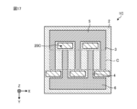
- FIG. 17 is a plan view showing a second modification of the elastic wave device according to the first embodiment.
- piezoelectric laminated structures 20C are arranged at intervals in the X direction.
- the piezoelectric laminated structure 20C does not overlap the electrode fingers 3 and 4 when viewed from above in the Z direction. Even in this case, since the excitation of elastic waves in the gap region is inhibited, leakage of elastic waves can be suppressed.
- FIG. 18 is an explanatory diagram showing an example of admittance characteristics of the elastic wave device according to the first embodiment.
- FIG. 19 is an explanatory diagram showing an example of admittance characteristics of the elastic wave device according to the first embodiment. More specifically, FIG. 18 is an explanatory diagram showing the real part of the admittance of the elastic wave device according to the first embodiment, that is, the conductance component.
- FIG. 19 is an explanatory diagram showing the scalar quantity of the admittance of the acoustic wave device according to the first embodiment, that is, the magnitude of the admittance only for modes occurring in the gap region.
- the example is the simulation result of the elastic wave device 1A according to the first embodiment
- the comparative example is the simulation result of the elastic wave device without the piezoelectric laminated structure 20 .
- the elastic wave device according to the example has a narrower peak width related to the resonance frequency than the elastic wave device according to the comparative example, so that the propagation loss is suppressed and the leakage of the elastic wave is reduced. is found to be suppressed.
- a mode derived from elastic wave leakage occurs in a band of 4 GHz to 6 GHz.
- the mode derived from leakage of the elastic wave does not occur in the pass band of 4 GHz or more and 6 GHz or less, but occurs in the band of 8 GHz or more and 12 GHz or less.
- the mode derived from leakage of elastic waves generated in the gap region does not couple with the mode of the main wave generated in the intersection region C, so that the elastic waves can be confined in the plane direction, and the elastic waves It can be seen that the leakage of
- the acoustic wave device 1A includes a support member including the support substrate 8 having a thickness in the first direction, the piezoelectric layer 2 provided in the first direction of the support member, and the piezoelectric layer 2 provided in the first direction.
- a plurality of first electrode fingers 3 provided on the main surface of the layer 2 and extending in a second direction intersecting the first direction; a first busbar electrode 5 to which the plurality of first electrode fingers 3 are connected;
- a plurality of second electrode fingers 4 facing any one of the plurality of first electrode fingers 3 in a third direction perpendicular to the direction and extending in the second direction, and a second bus bar to which the plurality of second electrode fingers 4 are connected.
- a piezoelectric laminated structure including a first piezoelectric body 21 and a second piezoelectric body 22 having a dielectric polarization state different from that of the first piezoelectric body 21 in a gap region between the two electrode fingers 4 and the first bus bar electrode 5. Includes body 20 .
- the piezoelectric laminated structure 20 overlaps the first electrode finger 3 or the second electrode finger 4 when viewed in plan in the first direction. Even in this case, leakage of elastic waves can be suppressed.
- the piezoelectric laminated structures 20 are arranged at intervals in the third direction. Even in this case, leakage of elastic waves can be suppressed.
- the thickness-shear primary mode bulk wave can be confined within the piezoelectric layer 2 .
- the supporting member includes, on the piezoelectric layer 2 side, one or more low acoustic impedance layers 42a, 42c, and 42e having an acoustic impedance lower than that of the piezoelectric layer 2 and one or more high acoustic impedance layers 42a, 42c, and 42e having an acoustic impedance higher than that of the piezoelectric layer 2. It has an acoustic reflection layer (acoustic multilayer film 42) including acoustic impedance layers 42b and 42d. As a result, the thickness-shear primary mode bulk wave can be confined within the piezoelectric layer 2 .
- the piezoelectric layer 2 in the intersection region C where the first electrode finger 3 and the second electrode finger 4 overlap has the same dielectric polarization state as the first piezoelectric body 21 . Even in this case, leakage of elastic waves can be suppressed.
- the direction of dielectric polarization of the first piezoelectric body 21 is opposite to the direction of dielectric polarization of the second piezoelectric body 22 . Thereby, leakage of elastic waves can be further suppressed.
- the piezoelectric layer 2 is Z-cut, and the second Euler angle ⁇ of the piezoelectric layer 2 is -15° or more and 15° or less. Even in this case, leakage of elastic waves can be suppressed.
- the thickness of the piezoelectric layer 2 is the center-to-center distance between the adjacent first electrode fingers 3 and the second electrode fingers 4 among the plurality of first electrode fingers 3 and the plurality of second electrode fingers 4. It is 2p or less when p.
- the piezoelectric layer 2 contains lithium niobate or lithium tantalate. As a result, it is possible to provide an elastic wave device capable of obtaining good resonance characteristics.
- it is configured to be able to use bulk waves in the thickness-shlip mode. As a result, it is possible to provide an elastic wave device with a high coupling coefficient and good resonance characteristics.
- the thickness of the piezoelectric layer 2 is d, and the center-to-center distance between the adjacent first electrode fingers 3 and second electrode fingers 4 among the plurality of first electrode fingers 3 and the plurality of second electrode fingers 4 is p. , d/p ⁇ 0.5.
- the acoustic wave device 1 can be miniaturized and the Q value can be increased.
- d/p is 0.24 or less.
- the region where the first electrode fingers 3 and the second electrode fingers 4 overlap when viewed in the third direction is the excitation region C, and the first electrode fingers 3 and the second electrode fingers 3 with respect to the excitation region C
- the metallization ratio of finger 4 is MR, MR ⁇ 1.75(d/p)+0.075 is satisfied.
- the fractional bandwidth can be reliably set to 17% or less.
- the piezoelectric layer 2 is made of lithium niobate or lithium tantalate, and the Euler angles ( ⁇ , ⁇ , ⁇ ) of lithium niobate or lithium tantalate satisfy the following formula (1), formula (2) or It is in the range of formula (3). In this case, the fractional bandwidth can be widened sufficiently.
- Equation (1) (0° ⁇ 10°, 20° to 80°, 0° to 60° (1-( ⁇ -50) 2 /900) 1/2 ) or (0° ⁇ 10°, 20° to 80°, [180 °-60° (1-( ⁇ -50)2/900) 1/2 ] ⁇ 180°) Equation (2) (0° ⁇ 10°, [180°-30°(1-( ⁇ -90) 2 /8100) 1/2 ] ⁇ 180°, arbitrary ⁇ ) Equation (3)
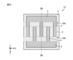
- FIG. 20 is a plan view showing an example of the elastic wave device according to the second embodiment.
- 21 is a cross-sectional view taken along line XXI-XXI of FIG. 20.
- FIG. An elastic wave device 1D according to the second embodiment will be described below with reference to the drawings.
- symbol is attached
- the thickness of the piezoelectric laminated structure 20D is different from the thickness of the piezoelectric layer 2 in the intersection region C.
- the thickness of the first piezoelectric layer is dp
- the thickness of the second piezoelectric layer is dp2
- the thickness of the piezoelectric layer 2 at the intersection region C is dp.
- the thickness (dp1+dp2) of the piezoelectric laminated structure 20 is 0.1 times or more the thickness dp of the piezoelectric layer 2 in the intersection area C. By setting it as this range, the leakage of an elastic wave can fully be suppressed.
- the thickness (dp1+dp2) of the piezoelectric laminated structure 20 is less than twice the thickness dp of the piezoelectric layer 2 in the intersection area C. As a result, it is possible to prevent the mode derived from leakage of the elastic wave from shifting to a low frequency, and to suppress the coupling with the main wave generated in the intersecting region C.
- the thickness (dp1+dp2) of the piezoelectric laminated structure 20 is equal to or greater than the thickness dp of the piezoelectric layer 2 in the intersection area C.
- the excitation mode of the piezoelectric laminate structure 20 occurs at a higher frequency than the excitation mode of the piezoelectric layer 2 in the intersection region C.
- the height (position in the Z direction) of the second main surface 20b of the piezoelectric laminated structure 20D is lower than the height of the second main surface 2b of the piezoelectric layer 2 .
- the direction of dielectric polarization of the first piezoelectric body 21 is the same upward direction as the piezoelectric layer 2 in the intersection region C.
- the direction of the dielectric polarization of the second piezoelectric body 22 is downward, opposite to that of the first piezoelectric body 21 , ie, the piezoelectric layer 2 in the intersection region C.
- the thickness dp1 of the first piezoelectric body 21 and the thickness dp2 of the second piezoelectric body 22 are equal.
- the thickness dp1 of the first piezoelectric body 21 and the thickness dp2 of the second piezoelectric body 22 may be different.
- the piezoelectric layer 2 in the intersection region C where the first electrode fingers 3 and the second electrode fingers 4 overlap when viewed in the third direction is the second piezoelectric layer 2 . It is in the same state of dielectric polarization as the body 22 . Even in this case, leakage of elastic waves can be suppressed.
- the thickness of the piezoelectric laminated structure 20 is less than twice the thickness of the piezoelectric layer 2 . As a result, it is possible to prevent the mode derived from leakage of the elastic wave from shifting to a low frequency, and to suppress the coupling with the main wave generated in the intersecting region C.
Landscapes
- Physics & Mathematics (AREA)
- Acoustics & Sound (AREA)
- Chemical & Material Sciences (AREA)
- Engineering & Computer Science (AREA)
- Ceramic Engineering (AREA)
- Surface Acoustic Wave Elements And Circuit Networks Thereof (AREA)
Priority Applications (3)
| Application Number | Priority Date | Filing Date | Title |
|---|---|---|---|
| JP2023540417A JP7540603B2 (ja) | 2021-08-04 | 2022-08-04 | 弾性波装置 |
| CN202280007223.3A CN116458063A (zh) | 2021-08-04 | 2022-08-04 | 弹性波装置 |
| US18/104,362 US20230170873A1 (en) | 2021-08-04 | 2023-02-01 | Acoustic wave device |
Applications Claiming Priority (2)
| Application Number | Priority Date | Filing Date | Title |
|---|---|---|---|
| US202163229082P | 2021-08-04 | 2021-08-04 | |
| US63/229,082 | 2021-08-04 |
Related Child Applications (1)
| Application Number | Title | Priority Date | Filing Date |
|---|---|---|---|
| US18/104,362 Continuation US20230170873A1 (en) | 2021-08-04 | 2023-02-01 | Acoustic wave device |
Publications (1)
| Publication Number | Publication Date |
|---|---|
| WO2023013742A1 true WO2023013742A1 (ja) | 2023-02-09 |
Family
ID=85155778
Family Applications (1)
| Application Number | Title | Priority Date | Filing Date |
|---|---|---|---|
| PCT/JP2022/030014 Ceased WO2023013742A1 (ja) | 2021-08-04 | 2022-08-04 | 弾性波装置 |
Country Status (4)
| Country | Link |
|---|---|
| US (1) | US20230170873A1 (https=) |
| JP (1) | JP7540603B2 (https=) |
| CN (1) | CN116458063A (https=) |
| WO (1) | WO2023013742A1 (https=) |
Families Citing this family (2)
| Publication number | Priority date | Publication date | Assignee | Title |
|---|---|---|---|---|
| US12237826B2 (en) * | 2018-06-15 | 2025-02-25 | Murata Manufacturing Co., Ltd. | Transversely-excited film bulk acoustic resonator with optimized electrode thickness, mark, and pitch |
| CN116686214A (zh) * | 2020-12-17 | 2023-09-01 | 株式会社村田制作所 | 弹性波装置 |
Citations (5)
| Publication number | Priority date | Publication date | Assignee | Title |
|---|---|---|---|---|
| JP2003332880A (ja) * | 2002-05-16 | 2003-11-21 | Fujitsu Media Device Kk | 弾性表面波素子 |
| JP2014110457A (ja) * | 2012-11-30 | 2014-06-12 | Kyocera Corp | 弾性波素子、分波器および通信モジュール |
| JP2019021997A (ja) * | 2017-07-12 | 2019-02-07 | 京セラ株式会社 | 弾性波素子、分波器および通信装置 |
| WO2020209359A1 (ja) * | 2019-04-12 | 2020-10-15 | 株式会社村田製作所 | 弾性波装置 |
| WO2021125013A1 (ja) * | 2019-12-19 | 2021-06-24 | 株式会社村田製作所 | 弾性波装置 |
Family Cites Families (2)
| Publication number | Priority date | Publication date | Assignee | Title |
|---|---|---|---|---|
| CN118285056A (zh) * | 2021-11-19 | 2024-07-02 | 株式会社村田制作所 | 弹性波装置 |
| JP2024114277A (ja) * | 2023-02-13 | 2024-08-23 | 株式会社村田製作所 | 弾性波装置 |
-
2022
- 2022-08-04 CN CN202280007223.3A patent/CN116458063A/zh active Pending
- 2022-08-04 WO PCT/JP2022/030014 patent/WO2023013742A1/ja not_active Ceased
- 2022-08-04 JP JP2023540417A patent/JP7540603B2/ja active Active
-
2023
- 2023-02-01 US US18/104,362 patent/US20230170873A1/en active Pending
Patent Citations (5)
| Publication number | Priority date | Publication date | Assignee | Title |
|---|---|---|---|---|
| JP2003332880A (ja) * | 2002-05-16 | 2003-11-21 | Fujitsu Media Device Kk | 弾性表面波素子 |
| JP2014110457A (ja) * | 2012-11-30 | 2014-06-12 | Kyocera Corp | 弾性波素子、分波器および通信モジュール |
| JP2019021997A (ja) * | 2017-07-12 | 2019-02-07 | 京セラ株式会社 | 弾性波素子、分波器および通信装置 |
| WO2020209359A1 (ja) * | 2019-04-12 | 2020-10-15 | 株式会社村田製作所 | 弾性波装置 |
| WO2021125013A1 (ja) * | 2019-12-19 | 2021-06-24 | 株式会社村田製作所 | 弾性波装置 |
Also Published As
| Publication number | Publication date |
|---|---|
| CN116458063A (zh) | 2023-07-18 |
| US20230170873A1 (en) | 2023-06-01 |
| JP7540603B2 (ja) | 2024-08-27 |
| JPWO2023013742A1 (https=) | 2023-02-09 |
Similar Documents
| Publication | Publication Date | Title |
|---|---|---|
| US20240250657A1 (en) | Acoustic wave device | |
| WO2022138457A1 (ja) | 弾性波装置 | |
| US20250023548A1 (en) | Acoustic wave device | |
| JP7540603B2 (ja) | 弾性波装置 | |
| WO2022085581A1 (ja) | 弾性波装置 | |
| WO2023090434A1 (ja) | 弾性波装置 | |
| WO2023140327A1 (ja) | 弾性波装置 | |
| WO2023191070A1 (ja) | 弾性波装置 | |
| WO2023085408A1 (ja) | 弾性波装置 | |
| WO2022210809A1 (ja) | 弾性波装置 | |
| WO2023002790A1 (ja) | 弾性波装置 | |
| US20250023553A1 (en) | Acoustic wave device | |
| US20240364295A1 (en) | Acoustic wave device | |
| WO2023171721A1 (ja) | 弾性波装置 | |
| WO2023013741A1 (ja) | 弾性波装置 | |
| WO2023140362A1 (ja) | 弾性波装置および弾性波装置の製造方法 | |
| WO2023145878A1 (ja) | 弾性波装置 | |
| WO2023223906A1 (ja) | 弾性波素子 | |
| WO2022255482A1 (ja) | 弾性波装置 | |
| WO2023204272A1 (ja) | 弾性波装置 | |
| WO2022211056A1 (ja) | 弾性波装置 | |
| WO2022211087A1 (ja) | 弾性波装置 | |
| WO2022124409A1 (ja) | 弾性波装置 | |
| US20230336140A1 (en) | Acoustic wave device | |
| WO2023286605A1 (ja) | 弾性波装置 |
Legal Events
| Date | Code | Title | Description |
|---|---|---|---|
| 121 | Ep: the epo has been informed by wipo that ep was designated in this application |
Ref document number: 22853160 Country of ref document: EP Kind code of ref document: A1 |
|
| WWE | Wipo information: entry into national phase |
Ref document number: 202280007223.3 Country of ref document: CN |
|
| WWE | Wipo information: entry into national phase |
Ref document number: 2023540417 Country of ref document: JP |
|
| NENP | Non-entry into the national phase |
Ref country code: DE |
|
| 122 | Ep: pct application non-entry in european phase |
Ref document number: 22853160 Country of ref document: EP Kind code of ref document: A1 |