WO2023013637A1 - ウエハ温度制御装置、ウエハ温度制御装置用制御方法、及び、ウエハ温度制御装置用プログラム - Google Patents
ウエハ温度制御装置、ウエハ温度制御装置用制御方法、及び、ウエハ温度制御装置用プログラム Download PDFInfo
- Publication number
- WO2023013637A1 WO2023013637A1 PCT/JP2022/029650 JP2022029650W WO2023013637A1 WO 2023013637 A1 WO2023013637 A1 WO 2023013637A1 JP 2022029650 W JP2022029650 W JP 2022029650W WO 2023013637 A1 WO2023013637 A1 WO 2023013637A1
- Authority
- WO
- WIPO (PCT)
- Prior art keywords
- temperature
- wafer
- cooler
- operation amount
- cooling
- Prior art date
- Legal status (The legal status is an assumption and is not a legal conclusion. Google has not performed a legal analysis and makes no representation as to the accuracy of the status listed.)
- Ceased
Links
Images


Classifications
-
- G—PHYSICS
- G05—CONTROLLING; REGULATING
- G05D—SYSTEMS FOR CONTROLLING OR REGULATING NON-ELECTRIC VARIABLES
- G05D23/00—Control of temperature
- G05D23/19—Control of temperature characterised by the use of electric means
-
- H—ELECTRICITY
- H10—SEMICONDUCTOR DEVICES; ELECTRIC SOLID-STATE DEVICES NOT OTHERWISE PROVIDED FOR
- H10P—GENERIC PROCESSES OR APPARATUS FOR THE MANUFACTURE OR TREATMENT OF DEVICES COVERED BY CLASS H10
- H10P72/00—Handling or holding of wafers, substrates or devices during manufacture or treatment thereof
- H10P72/70—Handling or holding of wafers, substrates or devices during manufacture or treatment thereof for supporting or gripping
- H10P72/76—Handling or holding of wafers, substrates or devices during manufacture or treatment thereof for supporting or gripping using mechanical means, e.g. clamps or pinches
- H10P72/7604—Handling or holding of wafers, substrates or devices during manufacture or treatment thereof for supporting or gripping using mechanical means, e.g. clamps or pinches the wafers being placed on a susceptor, stage or support
- H10P72/7624—Handling or holding of wafers, substrates or devices during manufacture or treatment thereof for supporting or gripping using mechanical means, e.g. clamps or pinches the wafers being placed on a susceptor, stage or support characterised by the mechanical construction of the susceptor, stage or support
-
- G—PHYSICS
- G05—CONTROLLING; REGULATING
- G05B—CONTROL OR REGULATING SYSTEMS IN GENERAL; FUNCTIONAL ELEMENTS OF SUCH SYSTEMS; MONITORING OR TESTING ARRANGEMENTS FOR SUCH SYSTEMS OR ELEMENTS
- G05B11/00—Automatic controllers
- G05B11/01—Automatic controllers electric
- G05B11/32—Automatic controllers electric with inputs from more than one sensing element; with outputs to more than one correcting element
-
- H—ELECTRICITY
- H10—SEMICONDUCTOR DEVICES; ELECTRIC SOLID-STATE DEVICES NOT OTHERWISE PROVIDED FOR
- H10P—GENERIC PROCESSES OR APPARATUS FOR THE MANUFACTURE OR TREATMENT OF DEVICES COVERED BY CLASS H10
- H10P72/00—Handling or holding of wafers, substrates or devices during manufacture or treatment thereof
- H10P72/04—Apparatus for manufacture or treatment
- H10P72/0431—Apparatus for thermal treatment
- H10P72/0434—Apparatus for thermal treatment mainly by convection
-
- H—ELECTRICITY
- H10—SEMICONDUCTOR DEVICES; ELECTRIC SOLID-STATE DEVICES NOT OTHERWISE PROVIDED FOR
- H10P—GENERIC PROCESSES OR APPARATUS FOR THE MANUFACTURE OR TREATMENT OF DEVICES COVERED BY CLASS H10
- H10P72/00—Handling or holding of wafers, substrates or devices during manufacture or treatment thereof
- H10P72/06—Apparatus for monitoring, sorting, marking, testing or measuring
- H10P72/0602—Temperature monitoring
-
- H—ELECTRICITY
- H10—SEMICONDUCTOR DEVICES; ELECTRIC SOLID-STATE DEVICES NOT OTHERWISE PROVIDED FOR
- H10P—GENERIC PROCESSES OR APPARATUS FOR THE MANUFACTURE OR TREATMENT OF DEVICES COVERED BY CLASS H10
- H10P95/00—Generic processes or apparatus for manufacture or treatments not covered by the other groups of this subclass
- H10P95/90—Thermal treatments, e.g. annealing or sintering
Definitions
- the present invention relates to a wafer temperature control device that controls the temperature of a wafer.
- the wafer temperature control device described in Patent Document 1 includes a stage having a cooling mechanism for cooling the wafer placed in the chamber and a heating mechanism for heating the wafer.
- the stage is made of a light-transmitting member, and has a coolant channel through which coolant flows.
- the cooling mechanism has a chiller connected to the coolant flow path inside the stage and outside the stage.
- the coolant supply is switched by controlling an open/close valve.
- the heating mechanism has a large number of LEDs provided on the opposite side of the stage from the wafer mounting surface. The light emitted from each LED is configured to irradiate the rear surface of the wafer after passing through the stage. Also, the amount of light emitted from each LED is controlled so that the temperature of the wafer reaches the target temperature.
- Patent Document 1 a temperature sensor is provided in the stage to measure the temperature in the vicinity of the wafer, and an observer estimates the temperature of the electronic devices formed on the wafer. Then, a current value corresponding to the temperature of the electronic device estimated by the observer is supplied to the LED to control the heating amount.
- Patent Document 1 does not use the cooling amount and the cooling operation amount as input parameters in the first place. difficult to control.
- the present invention has been made in view of the problems described above, and is capable of estimating a wafer temperature with sufficient accuracy and controlling the wafer temperature to a target temperature even when the cooling operation amount input to the cooler is changed. It is an object of the present invention to provide a wafer temperature control device capable of
- the wafer temperature control apparatus includes a heater that heats a wafer according to an input heating operation amount, a cooler that cools the wafer according to an input cooling operation amount, and a A wafer temperature based on a near temperature measuring device that measures a near temperature, the near temperature measured by the near temperature measuring device, and a cooling operation amount input to the cooler or a cooling amount output from the cooler and a temperature controller for controlling the cooling operation amount so as to reduce the temperature deviation between the set temperature and the estimated wafer temperature.
- a wafer temperature control method includes a heater that heats a wafer according to an input heating operation amount, and a cooler that cools the wafer according to an input cooling operation amount.
- a control method for a wafer temperature control device comprising: measuring a temperature in the vicinity of the wafer; the temperature in the vicinity measured by the temperature measuring device in the vicinity; estimating a wafer temperature based on an output cooling amount; and controlling the cooling operation amount so as to reduce a temperature deviation between a set temperature and the estimated wafer temperature. Characterized by
- the wafer temperature can be accurately estimated based on the neighboring temperature even when the cooling operation amount is changed. As a result, even if the wafer temperature cannot be actually measured, it is possible to keep the wafer temperature at the set temperature.
- the temperature estimation observer uses the wafer temperature and the neighboring temperature as output variables.
- a temperature estimation model which is a state space model, a vicinity temperature output unit that outputs the vicinity temperature estimated based on the temperature estimation model; and a wafer that outputs the wafer temperature estimated based on the temperature estimation model.
- a temperature output unit and an observer gain wherein the observer gain is applied to a deviation between the estimated value of the near temperature output from the near temperature output unit and the measured value of the near temperature output from the near temperature measuring device. It is sufficient that the value multiplied by is fed back into the temperature estimation model.
- the estimated wafer temperature will remain in a state of deviation from the actual temperature due to the influence of the disturbance.
- a value obtained by multiplying the integral value output from the observer integrator by the observer gain is fed back into the temperature estimation model.
- a configuration example suitable for heating or cooling the wafer housed in the chamber further includes a plate on which the wafer is placed, and the heater is configured to heat the plate. and wherein the cooler is configured to cool the plate.
- the cooler includes a coolant flow path and a coolant control section that controls the flow of the coolant flowing through the coolant flow path, and the cooling operation amount is the A wafer cooling amount or a target coolant flow rate can be mentioned.
- the temperature estimation model should be based on the amount of heating by the heater and the amount of heating by the cooler.
- a state space model in which a cooling amount is an input variable and the wafer temperature and the neighboring temperature are state variables, wherein the cooling amount is a difference between the wafer temperature and the neighboring temperature and a difference between the wafer and the plate. It may be calculated based on the heat transfer coefficient between.
- a heat transfer gas is supplied between the wafer and the plate at a predetermined pressure, and the heat transfer coefficient is It may be set based on the pressure of the transmission gas.
- the heating operation amount should be set at a constant value.
- the temperature controller may be constructed so that the state variable vector estimated by the temperature estimation observer is fed back.
- the temperature estimation observer can estimate the wafer temperature by considering the influence of the heating of the wafer by the gas present in the chamber or the heat radiation from the wafer, thereby further improving the estimation accuracy.
- the wafer temperature may be estimated based on the cooling operation amount or the cooling amount output by the cooler and the gas temperature measured by the gas temperature measuring device.
- the wafer is heated according to the input heating operation amount. and a cooler for cooling the wafer in accordance with an input cooling operation amount, the program for use in a wafer temperature control device, the near temperature measuring device for measuring the near temperature of the wafer. and a temperature estimation observer for estimating the wafer temperature based on the near temperature measured by the near temperature measuring device and the cooling operation amount input to the cooler or the cooling amount output by the cooler; and a temperature controller for controlling the cooling operation amount so that the temperature deviation between the temperature and the estimated wafer temperature becomes small. Just do it.
- the program for the wafer temperature control device may be electronically distributed, or may be recorded on a program recording medium such as a CD, DVD, or flash memory.
- the wafer temperature control apparatus of the present invention even when the cooling operation amount is changed, the wafer temperature, which is difficult to directly measure, can be accurately estimated. Further, since the cooling operation amount is controlled based on the temperature deviation between the wafer temperature estimated with high accuracy and the set temperature, it is possible to improve the control accuracy of the wafer temperature, for example.
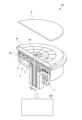
- FIG. 1 is a schematic perspective view of a wafer temperature control device according to a first embodiment of the present invention
- FIG. 1 is a schematic configuration diagram of a wafer temperature control device according to a first embodiment
- FIG. FIG. 2 is a schematic diagram expressing the wafer temperature control device according to the first embodiment using a state equation
- 2 is a functional block diagram showing the wafer temperature control device according to the first embodiment
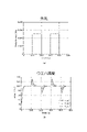
- FIG. 5 is a graph showing the relationship between the pressure of heat transfer gas supplied between the wafer and plate and the heat transfer coefficient between the wafer and plate in the first embodiment
- FIG. 2 is a schematic diagram for explaining modeling of the wafer temperature control device in the first embodiment
- 4 is a simulation result of the operation of the wafer temperature control device in the first embodiment
- FIG. 4 is a schematic diagram expressing the wafer temperature control device according to the second embodiment of the present invention in terms of state equations;
- FIG. 10 is a wafer temperature simulation result output from the temperature estimation observer of the second embodiment when a disturbance is input;
- FIG. 3 is a schematic configuration diagram of a wafer temperature control device according to a third embodiment of the present invention.
- FIG. 1 A wafer temperature control device 100 according to the first embodiment of the present invention will be described with reference to FIGS. 1 to 6.
- FIG. 1 A wafer temperature control device 100 according to the first embodiment of the present invention will be described with reference to FIGS. 1 to 6.
- the wafer temperature control device 100 of this embodiment is configured to electrostatically chuck the back surface of the wafer W in, for example, a vacuum chamber.
- the wafer temperature control apparatus 100 includes an adsorption plate AP having an approximately disk shape on which a wafer W is placed, and a cooler 2 provided so as to be in contact with the lower surface of the adsorption plate AP. , is equipped with
- the suction plate AP has a surface forming a suction surface, and a gas flow groove AP1 for supplying a heat transfer gas between the suction surface and the back surface of the wafer W being suctioned is formed.
- a gas flow groove AP1 for supplying a heat transfer gas between the suction surface and the back surface of the wafer W being suctioned is formed.
- helium gas is supplied to the gas flow groove AP1 at a predetermined pressure through a vertical through hole AP2 formed along the central axis of the adsorption plate AP and the cooler 2 .
- an electrostatic electrode (not shown) for generating an electrostatic force between the attraction plate AP and the wafer W is embedded in the attraction plate AP.
- a plurality of heater electrodes (not shown) for heating the adsorption plate AP are embedded in the adsorption plate AP, and these heaters constitute the heater 1 .
- heating amounts corresponding to heating operation amounts set by the user are output independently to heating control units (not shown) connected to the respective heater electrodes.
- the amount of heating can be made different between the central portion and the outer peripheral portion of the adsorption plate AP, and further, the amount of heating can be made different between the large area which is roughly C-shaped and the remaining small area in the outer peripheral portion. be able to. That is, three heating areas are set in the adsorption plate AP.
- the cooler 2 includes a substantially disk-shaped base plate BP in contact with the lower surface of the adsorption plate AP, a coolant flow path 21 formed in the base plate BP, and a coolant control for controlling the flow of the coolant flowing through the coolant flow path 21.
- the coolant channel 21 has a spiral shape within the base plate BP, and three cooling regions are formed on the surface of the base plate BP corresponding to the three heating regions of the adsorption plate AP.
- the coolant flows into or out of the coolant channel 21 in the base plate BP through a coolant inflow channel formed along the axial direction around the vertical through hole AP2 through which the helium gas flows. 22 or coolant outflow channel 23 .
- the coolant that flows through the base plate BP, cools the base plate BP, the adsorption plate AP, and the wafer W and rises in temperature is cooled again by a chiller (not shown) provided outside the base plate BP, and circulates through both of them. do.
- the refrigerant control unit changes the flow of the refrigerant flowing through the refrigerant flow path 21 according to the input cooling operation amount.
- the cooling operation amount is the target cooling amount, which is set as the heat amount
- the refrigerant control unit changes the opening degree of a control valve (not shown) that controls the refrigerant flow rate so as to achieve the target cooling amount.
- an infrared temperature sensor which is a near-field temperature measuring device 3 for measuring the near-field temperature of the wafer W, measures the temperature.
- the temperature measured by the infrared temperature sensor is the temperature of the base plate BP, it is not the temperature of the wafer W itself.
- the temperature of the wafer W in the vacuum chamber is not directly measured.
- the neighboring temperature is, for example, the temperature of a member or space within a predetermined distance from the wafer W, and it is possible to construct a temperature model showing the relationship between the wafer temperature and the neighboring temperature.
- the near-field temperature may include the temperature of a member to which heat can be conducted or transferred to or from the wafer W by at least one of conduction, convection, or radiation. More strictly, the temperature of a member in direct contact with the wafer W, the space or gas in which the interface with the wafer W exists, or the temperature of a member existing across a gap of several ⁇ m from the wafer W is defined as the near temperature. can also
- the wafer temperature control device 100 further includes a control device COM for controlling the operations of at least the heater 1 and the cooler 2, for example, outside the vacuum chamber.
- the control device COM is a so-called computer equipped with a CPU, a memory, an A/D converter, a D/A converter, and various input/output devices. Then, the wafer temperature control system program stored in the memory is executed, and the various devices work together to form a wafer temperature control system as shown in FIGS.
- the input cooling operation amount is sequentially changed based on the estimated wafer temperature or the actually measured neighboring temperature. More specifically, the temperature estimation observer 4 is used to estimate the wafer temperature, which cannot be measured directly, based on the nearby temperature measured by the infrared temperature sensor. Furthermore, the estimated wafer temperature and each state variable are fed back to control the cooler 2 so that the wafer temperature follows the set temperature.
- FIG. 4 is a functional block diagram detailing constituent elements for realizing each function. That is, the controlled object in this embodiment is a heat conduction and heat transfer system including the wafer W and the adsorption plate AP.
- the wafer temperature control apparatus 100 includes a temperature estimation observer 4 that simulates at least the thermal behavior of the system and estimates the temperature of the wafer W that cannot be directly measured, the estimated wafer temperature, and various parameters calculated by the temperature estimation observer 4 . It functions as a temperature controller 5 that feedback-controls the cooler 2 based on state variables.
- the temperature estimation observer 4 simulates the characteristics of the object to be controlled as shown in FIG. is configured to output an estimate of More specifically, the temperature estimation observer 4 includes a temperature estimation model 41, which is a state space model whose output variables are the wafer temperature and the neighborhood temperature, and a neighborhood temperature that outputs the neighborhood temperature estimated based on the temperature estimation model 41.
- a temperature output unit 43 a wafer temperature output unit 42 for outputting the wafer temperature estimated based on the temperature estimation model 41 , and an observer gain 44 are provided. Further, a value obtained by multiplying the difference between the estimated value of the nearby temperature output from the nearby temperature output unit 43 and the measured value of the nearby temperature output from the nearby temperature measuring device 3 by the observer gain 44 is obtained in the temperature estimation model 41. configured to be fed back to
- the temperature estimation model 41 is a model of heat conduction with respect to the adsorption plate AP and the wafer W itself, and heat transfer between the adsorption plate AP and the wafer W, for example. As shown in FIGS. 2, 3, and 4, only the temperature in the vicinity of the adsorption plate AP can actually be measured in the controlled object, so the controlled object cannot output the wafer temperature into the control loop. On the other hand, within the temperature estimation observer 4, the wafer temperature can be estimated by calculation based on the temperature estimation model 41 and output to the control loop.
- the input variable vector u(t) of the temperature estimation model 41 of this embodiment includes the cooling amount -q gi , which is the amount of heat output from the cooler 2 and removed from the wafer W, as an input variable.
- the suffix i indicates to which of the areas set on the attraction plate AP or the wafer W the parameter belongs, and the same applies to the following description.
- the heating amount qzi that is output from the heater 1 and applied to the wafer W is input as an input variable vector uheat.
- the heating amount q zi is treated as a fixed value because the heating operation amount is fixed in this embodiment.
- the cooling amount ⁇ q gi is sequentially calculated by the cooling amount calculator 6 .
- the cooling amount calculation unit 6 is based on a model of the heat transfer coefficient h with the helium gas pressure p and the separation distance d between the wafer W and the adsorption plate AP as variables as shown in the graph of FIG.
- a heat transfer coefficient h between the wafer W and the adsorption plate AP is determined.
- the cooling amount calculation unit 6 of the present embodiment is configured to calculate the cooling amount ⁇ qgi by multiplying the difference between the set temperature and the neighboring temperature of the wafer W by the calculated heat transfer coefficient h.
- the cooling amount -q gi depends on the pressure and flow rate of the helium gas, the temperature difference between the gas and the wafer, etc., and has complex characteristics including interactions and nonlinearity due to temperature changes.
- the temperature of the wafer W used in the cooling amount calculation unit 6 is set to a fixed value, and a function approximated around that temperature is derived.
- the difference ⁇ t between the wafer temperature and the temperature (near temperature) of the adsorption plate AP is calculated from the output of the temperature controller 5, and ⁇ t is multiplied by the determined heat transfer coefficient h. may be configured to calculate the cooling amount ⁇ q gi .
- the output variable vector y(t) in FIGS. 3 and 4 includes the wafer temperature Twi and the neighboring temperature Tpi , which is the temperature of the suction plate AP, as output variables.
- the state variable vector x(t) also includes the wafer temperature T wi and the neighboring temperature T pi that is the temperature of the suction plate AP as state variables.
- A, B, B2, Cr, and C may be determined based on a heat conduction equation or a relational expression of heat transfer, or each element of each matrix may be determined based on experiments or the like.
- An outer peripheral C-shaped region W1, a central region W2, and an outer peripheral fan-shaped region W3 are set on the wafer W, and a contact C-shaped region P1 that contacts the outer peripheral C-shaped region W1 of the wafer W on the suction plate AP, the wafer A contact central region P2 in contact with the central region W2 of W, a contact fan-shaped region P3 in contact with the outer peripheral fan-shaped region W3 of the wafer W, a non-contact C-shaped region P4 outside the wafer W and not in contact with the wafer W, outside the wafer , and when a non-contact fan-shaped region P5 that does not come into contact with the wafer W and a protruding region P6 that protrudes further outward from the non-contact fan-shaped region P5 are set, the correspondence relationship between each row of the state matrix A and the actual system is shown in FIG. as shown.
- the elements of each row of the state matrix A are set to values calculated based on, for example, heat conduction coefficients that
- the input matrix B defines the cooling characteristics of each region of the wafer W by the helium gas described above.
- the input matrix B2 defines the heating characteristics of the heater electrodes.
- the output matrices Cr and C are defined only by a zero matrix and a unit matrix. Further, the state of the state variable vector x(t) is fed back to the temperature controller 5 .
- the wafer temperature output unit 42 extracts only the elements corresponding to the wafer temperature from the output of the temperature estimation model 41 and outputs them to the temperature controller 5 .
- the wafer temperature output unit 42 corresponds to the output matrix C.
- the neighborhood temperature output unit 43 extracts and outputs only elements corresponding to the neighborhood temperature from the output of the temperature estimation model 41 . A deviation between the output estimated value of the nearby temperature and the measured value of the nearby temperature output from the nearby temperature measuring device 3 is calculated and input to the observer gain 44 .
- the neighborhood temperature output unit 43 corresponds to the output matrix Cr in this embodiment.
- the temperature controller 5 multiplies the temperature deviation between the wafer temperature estimated by the temperature estimation observer 4 and the set temperature by a gain K to perform integral calculation. Also, the deviation between the calculated integrated value and the value obtained by multiplying the state variable vector x(t) by a predetermined state feedback gain F is calculated, and this deviation is input to the cooler 2 as a cooling operation amount.
- FIG. 7 shows a simulation result of the operation when 100° C. is set as the set temperature in the wafer temperature control device 100 configured as described above.
- the temperature of each region of the wafer W reaches the set temperature of 100° C. with substantially the same first-order lag characteristics, based on the wafer temperature estimated by the temperature estimation observer 4 . It can be seen that it is possible to control
- the temperature estimation observer 4 estimates a wafer temperature that cannot be actually measured, and feeds back the estimated value of the wafer temperature and other state variables. It becomes possible to keep the wafer temperature at the set temperature.
- the output of the heater 1 is kept constant, and the output of the cooler 2 is controlled by temperature feedback control and state feedback control. High-precision control can be realized without shooting or the like.
- the wafer temperature control device 100 of the second embodiment takes into consideration the influence on the temperature estimation observer 4 when the disturbance d is input to the system.
- the temperature estimation observer 4 of the wafer temperature control apparatus 100 of the second embodiment differs from that of the first embodiment in that an observer integrator 45 is provided. More specifically, in the temperature estimation observer 4, the difference between the estimated value of the nearby temperature and the measured value of the nearby temperature measuring device 3 is fed back to the temperature estimation model 41, and in parallel, the integrated value of the deviation is calculated. is also fed back to the temperature estimation model 41 .
- the temperature estimation observer 4 includes a first feedback loop that feeds back to the temperature estimation model 41 a value obtained by multiplying the difference between the estimated value of the nearby temperature and the measured value by the proportional observer gain 441, and the difference between the estimated value of the nearby temperature and the measured value. and a second feedback loop that integrates the deviation by an observer integrator 45 and feeds back a value obtained by multiplying the integrated value by an integral observer gain 442 to the temperature estimation model 41 .
- the proportional observer gain 441 and the integral observer gain 442 correspond to the observer gain 44 in the first embodiment.
- FIG. 9(b) shows simulation results regarding wafer temperature estimation by the temperature estimation observer 4 of the second embodiment when periodic disturbance d occurs as shown in FIG. 9(a).
- the estimated value of the wafer temperature and the control result are adjusted to the set temperature so as to cancel out the disturbance.
- the wafer temperature estimated by the temperature estimation observer 4 may continue to deviate from the actual wafer temperature. If so, such an estimation error can be eliminated, and even if the disturbance d is input, the actual wafer temperature can finally be estimated.
- the wafer temperature control apparatus 100 of the third embodiment further includes a gas temperature measuring device GT for measuring the temperature of the gas present near the upper side of the wafer W in the chamber.
- the wafer temperature is estimated using not only the adjacent temperature measured by the adsorption plate AP measured at , but also the gas temperature measured by the gas temperature measuring device GT.
- the gas temperature measuring device GT is, for example, an absorption analyzer configured to measure the gas temperature based on the absorbance of laser light passing right above the wafer W along the direction of the face plate.
- the state vector x used in the temperature estimation model can include not only the wafer temperature and the neighboring temperature, but also the gas temperature.
- the gas temperature is only included as a component in the state vector x of the state equation described in the first embodiment, and other matrices and vectors can be handled in the same way.
- the wafer temperature estimated based on such an equation of state can be improved in estimation accuracy by the amount of information on actually measured temperatures, and thus the wafer temperature control accuracy can be further improved.
- the heating operation amount of the heater may also be changed by output feedback control or state feedback control.
- the temperature estimation observer may be configured as a Kalman filter in consideration of disturbance effects.
- Various existing methods may be used to set the Kalman gain instead of the observer gain.
- the method of calculating the amount of cooling used as an input variable is not limited to the modeling method described above. For example, it may be calculated as an approximated value assuming that the temperature difference between the wafer and the suction plate is a constant value.
- the cooler or heater is not limited to those mentioned above.
- the cooler may be configured using a Peltier element or the like, and the heater is not limited to the heater electrode, and may be configured to heat the wafer by light irradiation.
- the heating or cooling areas of the wafer and the suction plate are not limited to three areas, but may be divided into a larger number of areas or may be divided into two areas. .
- the entire wafer or suction plate may be treated as one temperature without setting the region.
- the suction plate may be simply a plate on which the wafer is placed without a suction function.
- the location where the nearby temperature measuring instrument measures is not limited to the locations described above, and may be other locations. In short, a temperature that seems to have some kind of correlation or relationship with the wafer temperature should be measured as the neighboring temperature.
- the temperature controller is not limited to the infrared temperature sensor, and may be, for example, a thermocouple provided in the plate.
- the integrated value of the deviation is fed back to the temperature estimation model together with the deviation between the measured value and the estimated value of the nearby temperature.
- the integrated value of the deviation is fed back to the temperature estimation model. may be made.
- the wafer temperature which is difficult to directly measure, can be estimated with high accuracy.
- a control device can be provided.
- Wafer temperature control device 1 Heater 2: Cooler 21: Coolant channel 3: Nearby temperature measuring device 4: Temperature estimation observer 5: Temperature controller 41: Temperature estimation model 42: Wafer temperature output unit 43: Nearby temperature Output unit 44: observer gain AP: adsorption plate BP: base plate
Landscapes
- Physics & Mathematics (AREA)
- General Physics & Mathematics (AREA)
- Engineering & Computer Science (AREA)
- Automation & Control Theory (AREA)
- Control Of Temperature (AREA)
Priority Applications (4)
| Application Number | Priority Date | Filing Date | Title |
|---|---|---|---|
| JP2023540362A JPWO2023013637A1 (https=) | 2021-08-06 | 2022-08-02 | |
| CN202280052970.9A CN117730292A (zh) | 2021-08-06 | 2022-08-02 | 晶圆温度控制装置、晶圆温度控制装置用控制方法及晶圆温度控制装置用程序 |
| US18/681,369 US20250372417A1 (en) | 2021-08-06 | 2022-08-02 | Wafer temperature control device, control method for wafer temperature control device, and program for wafer temperature control device |
| KR1020247005982A KR20240045237A (ko) | 2021-08-06 | 2022-08-02 | 웨이퍼 온도 제어 장치, 웨이퍼 온도 제어 장치용 제어 방법, 및 웨이퍼 온도 제어 장치용 프로그램 |
Applications Claiming Priority (2)
| Application Number | Priority Date | Filing Date | Title |
|---|---|---|---|
| JP2021130031 | 2021-08-06 | ||
| JP2021-130031 | 2021-08-06 |
Publications (1)
| Publication Number | Publication Date |
|---|---|
| WO2023013637A1 true WO2023013637A1 (ja) | 2023-02-09 |
Family
ID=85155628
Family Applications (1)
| Application Number | Title | Priority Date | Filing Date |
|---|---|---|---|
| PCT/JP2022/029650 Ceased WO2023013637A1 (ja) | 2021-08-06 | 2022-08-02 | ウエハ温度制御装置、ウエハ温度制御装置用制御方法、及び、ウエハ温度制御装置用プログラム |
Country Status (6)
| Country | Link |
|---|---|
| US (1) | US20250372417A1 (https=) |
| JP (1) | JPWO2023013637A1 (https=) |
| KR (1) | KR20240045237A (https=) |
| CN (1) | CN117730292A (https=) |
| TW (1) | TW202314429A (https=) |
| WO (1) | WO2023013637A1 (https=) |
Cited By (2)
| Publication number | Priority date | Publication date | Assignee | Title |
|---|---|---|---|---|
| CN117311184A (zh) * | 2023-10-31 | 2023-12-29 | 深圳市华翌科技有限公司 | 一种基于物联网的智能家居调控系统 |
| WO2025191634A1 (ja) * | 2024-03-11 | 2025-09-18 | 株式会社日立ハイテク | プラズマ処理装置 |
Citations (3)
| Publication number | Priority date | Publication date | Assignee | Title |
|---|---|---|---|---|
| JP2001318720A (ja) * | 2000-05-08 | 2001-11-16 | Komatsu Ltd | 温度制御方法及び装置 |
| JP2004119630A (ja) * | 2002-09-25 | 2004-04-15 | Komatsu Ltd | ウェハ温調装置 |
| JP2014081350A (ja) * | 2012-09-28 | 2014-05-08 | Tokyo Electron Ltd | 温度測定機構及び温度測定方法 |
Family Cites Families (1)
| Publication number | Priority date | Publication date | Assignee | Title |
|---|---|---|---|---|
| JP7266481B2 (ja) | 2019-07-19 | 2023-04-28 | 東京エレクトロン株式会社 | 温度制御装置、温度制御方法、および検査装置 |
-
2022
- 2022-08-02 CN CN202280052970.9A patent/CN117730292A/zh active Pending
- 2022-08-02 WO PCT/JP2022/029650 patent/WO2023013637A1/ja not_active Ceased
- 2022-08-02 US US18/681,369 patent/US20250372417A1/en active Pending
- 2022-08-02 JP JP2023540362A patent/JPWO2023013637A1/ja active Pending
- 2022-08-02 KR KR1020247005982A patent/KR20240045237A/ko active Pending
- 2022-08-04 TW TW111129413A patent/TW202314429A/zh unknown
Patent Citations (3)
| Publication number | Priority date | Publication date | Assignee | Title |
|---|---|---|---|---|
| JP2001318720A (ja) * | 2000-05-08 | 2001-11-16 | Komatsu Ltd | 温度制御方法及び装置 |
| JP2004119630A (ja) * | 2002-09-25 | 2004-04-15 | Komatsu Ltd | ウェハ温調装置 |
| JP2014081350A (ja) * | 2012-09-28 | 2014-05-08 | Tokyo Electron Ltd | 温度測定機構及び温度測定方法 |
Cited By (4)
| Publication number | Priority date | Publication date | Assignee | Title |
|---|---|---|---|---|
| CN117311184A (zh) * | 2023-10-31 | 2023-12-29 | 深圳市华翌科技有限公司 | 一种基于物联网的智能家居调控系统 |
| WO2025191634A1 (ja) * | 2024-03-11 | 2025-09-18 | 株式会社日立ハイテク | プラズマ処理装置 |
| JPWO2025191634A1 (https=) * | 2024-03-11 | 2025-09-18 | ||
| KR20250138715A (ko) | 2024-03-11 | 2025-09-22 | 주식회사 히타치하이테크 | 플라스마 처리 장치 |
Also Published As
| Publication number | Publication date |
|---|---|
| US20250372417A1 (en) | 2025-12-04 |
| KR20240045237A (ko) | 2024-04-05 |
| JPWO2023013637A1 (https=) | 2023-02-09 |
| TW202314429A (zh) | 2023-04-01 |
| CN117730292A (zh) | 2024-03-19 |
Similar Documents
| Publication | Publication Date | Title |
|---|---|---|
| US20240047246A1 (en) | Advanced temperature control for wafer carrier in plasma processing chamber | |
| WO2023013637A1 (ja) | ウエハ温度制御装置、ウエハ温度制御装置用制御方法、及び、ウエハ温度制御装置用プログラム | |
| CN1910517B (zh) | 光罩/掩模系统的自适应实时控制 | |
| US6461438B1 (en) | Heat treatment unit, cooling unit and cooling treatment method | |
| JP2024106711A (ja) | ウエハ温度制御装置、ウエハ温度制御方法及びウエハ温度制御プログラム | |
| CN107636817A (zh) | 方位可调整的多区域静电夹具 | |
| US20080228308A1 (en) | Critical dimension uniformity optimization | |
| CN107430985B (zh) | 热处理装置以及热处理方法 | |
| US12106979B2 (en) | Apparatus and method for controlling temperature uniformity of substrate | |
| JP7284850B2 (ja) | ジェット・アンド・フラッシュ・インプリントリソグラフィにおけるマルチフィールドオーバーレイ制御 | |
| JP7796625B2 (ja) | ウエハ温度制御装置、ウエハ温度制御方法及びウエハ温度制御プログラム | |
| JP6405133B2 (ja) | 半導体ウェーハの温度制御装置、半導体ウェーハの温度制御方法 | |
| Koch et al. | Sliding mode control of a distributed-parameter wafer spin clean process | |
| US12438012B2 (en) | Automatic control of substrates | |
| US20250006524A1 (en) | Wafer temperature control device, wafer temperature control method and wafer temperature control program | |
| CN118763032A (zh) | 一种用于刻蚀中载台的温度补偿方法及装置 | |
| JP2017174011A (ja) | 半導体ウェーハの温度制御装置、および半導体ウェーハの温度制御方法 | |
| JP3966490B2 (ja) | 基板温度推定装置及び方法、並びにそれを用いた基板温度制御装置 | |
| TWI911934B (zh) | 溫度補償方法、溫度補償裝置和製程腔室 | |
| TWI878646B (zh) | 光源裝置及校準裝置 | |
| US20250218736A1 (en) | Apparatus and method for controlling temperature | |
| WO2024034355A1 (ja) | パラメータ推定システム、パラメータ推定方法、コンピュータプログラム及び基板処理装置 | |
| CN121115925A (zh) | 一种控温方法、静电卡盘及半导体工艺设备 | |
| KR20240033506A (ko) | 기판 처리 장치 및 기판 처리 방법 |
Legal Events
| Date | Code | Title | Description |
|---|---|---|---|
| 121 | Ep: the epo has been informed by wipo that ep was designated in this application |
Ref document number: 22853056 Country of ref document: EP Kind code of ref document: A1 |
|
| WWE | Wipo information: entry into national phase |
Ref document number: 2023540362 Country of ref document: JP |
|
| WWE | Wipo information: entry into national phase |
Ref document number: 202280052970.9 Country of ref document: CN |
|
| NENP | Non-entry into the national phase |
Ref country code: DE |
|
| 122 | Ep: pct application non-entry in european phase |
Ref document number: 22853056 Country of ref document: EP Kind code of ref document: A1 |