WO2023002852A1 - 半導体装置、スイッチング電源、発光装置 - Google Patents
半導体装置、スイッチング電源、発光装置 Download PDFInfo
- Publication number
- WO2023002852A1 WO2023002852A1 PCT/JP2022/026940 JP2022026940W WO2023002852A1 WO 2023002852 A1 WO2023002852 A1 WO 2023002852A1 JP 2022026940 W JP2022026940 W JP 2022026940W WO 2023002852 A1 WO2023002852 A1 WO 2023002852A1
- Authority
- WO
- WIPO (PCT)
- Prior art keywords
- signal
- voltage
- output
- detection signal
- current
- Prior art date
- Legal status (The legal status is an assumption and is not a legal conclusion. Google has not performed a legal analysis and makes no representation as to the accuracy of the status listed.)
- Ceased
Links
Images





Classifications
-
- H—ELECTRICITY
- H05—ELECTRIC TECHNIQUES NOT OTHERWISE PROVIDED FOR
- H05B—ELECTRIC HEATING; ELECTRIC LIGHT SOURCES NOT OTHERWISE PROVIDED FOR; CIRCUIT ARRANGEMENTS FOR ELECTRIC LIGHT SOURCES, IN GENERAL
- H05B45/00—Circuit arrangements for operating light-emitting diodes [LED]
- H05B45/30—Driver circuits
- H05B45/37—Converter circuits
- H05B45/3725—Switched mode power supply [SMPS]
-
- H—ELECTRICITY
- H02—GENERATION; CONVERSION OR DISTRIBUTION OF ELECTRIC POWER
- H02M—APPARATUS FOR CONVERSION BETWEEN AC AND AC, BETWEEN AC AND DC, OR BETWEEN DC AND DC, AND FOR USE WITH MAINS OR SIMILAR POWER SUPPLY SYSTEMS; CONVERSION OF DC OR AC INPUT POWER INTO SURGE OUTPUT POWER; CONTROL OR REGULATION THEREOF
- H02M3/00—Conversion of DC power input into DC power output
- H02M3/02—Conversion of DC power input into DC power output without intermediate conversion into AC
- H02M3/04—Conversion of DC power input into DC power output without intermediate conversion into AC by static converters
- H02M3/10—Conversion of DC power input into DC power output without intermediate conversion into AC by static converters using discharge tubes with control electrode or semiconductor devices with control electrode
- H02M3/145—Conversion of DC power input into DC power output without intermediate conversion into AC by static converters using discharge tubes with control electrode or semiconductor devices with control electrode using devices of a triode or transistor type requiring continuous application of a control signal
- H02M3/155—Conversion of DC power input into DC power output without intermediate conversion into AC by static converters using discharge tubes with control electrode or semiconductor devices with control electrode using devices of a triode or transistor type requiring continuous application of a control signal using semiconductor devices only
-
- H—ELECTRICITY
- H05—ELECTRIC TECHNIQUES NOT OTHERWISE PROVIDED FOR
- H05B—ELECTRIC HEATING; ELECTRIC LIGHT SOURCES NOT OTHERWISE PROVIDED FOR; CIRCUIT ARRANGEMENTS FOR ELECTRIC LIGHT SOURCES, IN GENERAL
- H05B45/00—Circuit arrangements for operating light-emitting diodes [LED]
- H05B45/10—Controlling the intensity of the light
- H05B45/14—Controlling the intensity of the light using electrical feedback from LEDs or from LED modules
-
- H—ELECTRICITY
- H05—ELECTRIC TECHNIQUES NOT OTHERWISE PROVIDED FOR
- H05B—ELECTRIC HEATING; ELECTRIC LIGHT SOURCES NOT OTHERWISE PROVIDED FOR; CIRCUIT ARRANGEMENTS FOR ELECTRIC LIGHT SOURCES, IN GENERAL
- H05B45/00—Circuit arrangements for operating light-emitting diodes [LED]
- H05B45/30—Driver circuits
- H05B45/32—Pulse-control circuits
-
- H—ELECTRICITY
- H05—ELECTRIC TECHNIQUES NOT OTHERWISE PROVIDED FOR
- H05B—ELECTRIC HEATING; ELECTRIC LIGHT SOURCES NOT OTHERWISE PROVIDED FOR; CIRCUIT ARRANGEMENTS FOR ELECTRIC LIGHT SOURCES, IN GENERAL
- H05B45/00—Circuit arrangements for operating light-emitting diodes [LED]
- H05B45/30—Driver circuits
- H05B45/34—Voltage stabilisation; Maintaining constant voltage
-
- H—ELECTRICITY
- H05—ELECTRIC TECHNIQUES NOT OTHERWISE PROVIDED FOR
- H05B—ELECTRIC HEATING; ELECTRIC LIGHT SOURCES NOT OTHERWISE PROVIDED FOR; CIRCUIT ARRANGEMENTS FOR ELECTRIC LIGHT SOURCES, IN GENERAL
- H05B45/00—Circuit arrangements for operating light-emitting diodes [LED]
- H05B45/30—Driver circuits
- H05B45/345—Current stabilisation; Maintaining constant current
-
- H—ELECTRICITY
- H05—ELECTRIC TECHNIQUES NOT OTHERWISE PROVIDED FOR
- H05B—ELECTRIC HEATING; ELECTRIC LIGHT SOURCES NOT OTHERWISE PROVIDED FOR; CIRCUIT ARRANGEMENTS FOR ELECTRIC LIGHT SOURCES, IN GENERAL
- H05B45/00—Circuit arrangements for operating light-emitting diodes [LED]
- H05B45/50—Circuit arrangements for operating light-emitting diodes [LED] responsive to malfunctions or undesirable behaviour of LEDs; responsive to LED life; Protective circuits
Definitions
- the invention disclosed in this specification relates to a semiconductor device, and a switching power supply and a light emitting device using the same.
- a semiconductor device for example, an LED [light emitting diode] driver IC or a power supply controller IC that functions as a part of a switching power supply is widely used.
- Patent Document 1 can be cited as an example of conventional technology related to the above.
- the invention disclosed in the present specification provides a semiconductor device capable of arbitrarily switching the target of output feedback control in a switching power supply, and a semiconductor device using the same. It is an object of the present invention to provide a switching power supply and a light-emitting device that have
- the semiconductor device disclosed in this specification is configured to function as a component of a switching power supply, and amplifies a sense voltage corresponding to the inductor current of the switching power supply to generate a current detection signal.
- a voltage detection signal generator configured to generate a voltage detection signal according to the output voltage of the switching power supply; and the current detection signal according to a mode switching signal.
- a selector configured to output one of the voltage detection signals as a selection detection signal, and an output feedback control section configured to drive and control the switching power supply based on the selection detection signal.
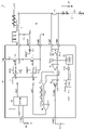
- FIG. 1 is a diagram showing a first comparative example of an LED light emitting device.
- FIG. 2 is a diagram showing output feedback control (constant current control) of the bottom detection on-time fixed system.
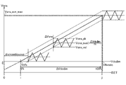
- FIG. 3 is a diagram showing an example of dimming control.
- FIG. 4 is a diagram showing a second comparative example of the LED light emitting device.
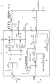
- FIG. 5 is a diagram showing a first embodiment of an LED light emitting device.
- FIG. 6 is a diagram showing output feedback control (constant voltage control) of the bottom detection on-time fixed system.
- FIG. 7 is a diagram showing a second embodiment of the LED light emitting device.
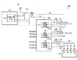
- FIG. 8 is a diagram showing a third embodiment of the LED light emitting device.
- FIG. 9 is a diagram showing a fourth embodiment of the LED light emitting device.
- FIG. 10 is a diagram showing a fifth embodiment of the LED light emitting device.
- the switching power supply X is configured using the LED driver IC 10 and various discrete components (capacitors Cb, Cc and Co, inductor L, resistor Rt and sense resistor Rs) externally attached to this.
- the LED driver IC 10 is a semiconductor device that functions as a part of the switching power supply X that steps down the power system input voltage Vi to supply power to the LED load Z.
- the LED driver IC 10 has a plurality of external terminals (PIN pin, SW pin, BOOT pin, PGND pin, SNSP pin, SNSN pin, TON pin and COMP pin, etc.).
- the PIN pin is a power system power supply terminal.
- the SW pin is a switch output terminal.
- the BOOT pin is the bootstrap capacitor connection terminal for the upper gate drive.
- a PGND pin is a power system ground terminal.
- the SNSP pin is the first current sense terminal (+).
- the SNSN pin is the second current sense terminal (-).
- the TON pin is a resistor connection terminal for setting ON time.
- a COMP pin is a capacitor connection terminal for phase compensation.
- the PIN pin is connected to the power supply terminal (input voltage Vi application terminal) of the power system.
- the SW pin is connected to the first end of inductor L.
- a second end of the inductor L is connected to a first end of the sense resistor Rs.
- a second end of the sense resistor Rs is connected to the anode of the LED load Z.
- the cathode of the LED load Z is connected to ground.
- a capacitor Cb bootsstrap capacitor
- a capacitor Co output capacitor
- a first end (high potential end) of the sense resistor Rs is connected to the SNSP pin.
- a second end (low potential end) of the sense resistor Rs is connected to the SNSN pin.
- the PGND pin is connected to the ground end of the power system.
- a resistor Rt on-time setting resistor
- a capacitor Cc phase compensation capacitor
- the LED driver IC 10 of the first comparative example includes, as means for driving the LED load Z, an upper switch 11H, a lower switch 11L, an upper driver 12H, a lower driver 12L, a controller 13, an on-time setting section 14, current sense amplifier 15, error amplifier 16, slope signal generator 17, comparator 18, DAC [digital-to-analog converter] 19, VI converter 20, bootstrap It contains diode D1 and input resistors R1P and R1N.
- the LED driver IC 10 may be integrated with components other than the above (temperature detection circuit, various protection circuits, etc.).
- the upper switch 11H is connected between the PIN pin and the SW pin and turned on/off according to the upper gate signal GH.
- the lower switch 11L is connected between the SW pin and the PGND pin and turned on/off according to the lower gate signal GL.
- the inductor L, sense resistor Rs, and LED load Z described above are connected in series to the upper switch 11H.
- a synchronous rectification half-bridge output stage is shown, but in the case of adopting a diode rectification method, a diode may be used as the lower switch 11L.
- the upper switch 11H and the lower switch 11L may be externally attached to the LED driver IC 10.
- the upper driver 12H generates the upper gate signal GH based on the upper control signal SH input from the controller 13.
- the high level of the upper gate signal GH becomes the boost voltage Vbst ( ⁇ Vsw+5VEXT) appearing at the BOOT pin.
- the low level of the upper gate signal GH becomes the switch voltage Vsw appearing at the SW pin.
- the lower driver 12L generates the lower gate signal GL based on the lower control signal SL input from the controller 13.
- the high level of the lower gate signal GL is the constant voltage 5VEXT (internal power supply voltage or separate external input voltage).
- the low level of the lower gate signal GL becomes the terminal voltage (power system ground voltage) of the PGND pin.
- the controller 13 includes, for example, an RS flip-flop that receives inputs of a set signal SET and a reset signal RST, and outputs an upper control signal SH and a lower control signal to complementarily turn on/off the upper switch 11H and the lower switch 11L. Generate SL.
- the controller 13 turns on the upper switch 11H and turns off the lower switch 11L at the rise timing of the set signal SET, and turns off the upper switch 11H and turns off the lower switch 11L at the rise timing of the reset signal RST.
- An upper control signal SH and a lower control signal SL are generated to turn on the switch 11L.
- the term "complementary" in this specification is used not only when the on/off states of the upper switch 11H and the lower switch 11L are completely reversed, but also when the simultaneous off state to prevent shoot-through current is used. It should be understood in a broad sense as including the case where a period (so-called dead time) is provided.
- the on-time setting unit 14 raises the reset signal RST to a high level when a predetermined on-time Ton elapses from the rising timing of the set signal SET (and the on timing of the upper switch 11H).
- the on-time setting unit 14 has a function of arbitrarily setting the on-time Ton according to the resistance value of the resistor Rt connected to the TON pin.
- the on-time setting unit 14 also has a function of varying the on-time Ton based on the terminal voltages of the PIN pin and the SNSP pin (or the SNSN pin) so as to suppress variations in the switching frequency Fsw.
- the current sense amplifier 15 is a differential output amplifier with a floating input stage capable of rail-to-rail amplification of the input signal.
- floating means floating (potentially separated) from the ground potential.
- the non-inverting input terminal (+) of the current sense amplifier 15 is connected to the first terminal of the input resistor R1P (eg, 10 k ⁇ ).
- the second end of input resistor R1P is connected to the SNSP pin.
- the inverting input terminal (-) of the current sense amplifier 15 is connected to the first terminal of the input resistor R1N (eg, 10 k ⁇ ).
- a second end of input resistor R1N is connected to the SNSN pin.
- a VI converter 20 is connected to the non-inverting input terminal (+) and the inverting input terminal (-) of the current sense amplifier 15 .
- the error amplifier 16 outputs a current according to the differential current detection signal VISET, and generates an error signal Vcomp by charging and discharging a phase compensation capacitor Cc externally attached to the COMP pin.
- the error signal Vcomp increases when the current detection signal VISET becomes negative voltage, and conversely decreases when the current detection signal VISET becomes positive voltage.
- the transconductance gm of the error amplifier 16 may be a variable value according to the register value GM.
- the slope signal Vcso takes the error signal Vcomp as the bottom value, and has a triangular waveform that increases as the inductor current IL increases and conversely decreases as the inductor current IL decreases.
- the comparator 18 generates the set signal SET by comparing the slope signal Vcso input to the inverting input terminal (-) and the error signal Vcomp input to the non-inverting input terminal (+).
- the set signal SET becomes low level when Vcomp ⁇ Vcso, and becomes high level when Vcomp>Vcso. Therefore, the lower the error signal Vcomp, the later the rise timing of the set signal SET (and the ON timing of the upper switch 11H), and the higher the error signal Vcomp, the earlier the set signal SET rise timing.
- Such a comparison operation of the comparator 18 is equivalent to a bottom detection operation (valley detection operation) of the inductor current IL.
- the digital dimming signal ISET is a digital register value set from the outside of the LED driver IC 10 via an arbitrary interface (SPI [serial peripheral interface], etc.).
- the analog dimming signal Vdcdim is a voltage signal that varies within a predetermined range (0 to Vfsradc, where Vfsradc is the power supply voltage of the DAC 19) according to the digital dimming signal ISET.
- the VI converter 20 corresponds to a sense voltage adjustment section that adjusts the sense voltage Vsns according to the analog dimming signal Vdcdim.
- the VI converter 20 converts the analog dimming signal Vdcdim into a current signal and uses the same current signal to adjust the currents flowing through the input resistors R1P and R1N, respectively.
- An arbitrary offset signal Vofs may be applied to the analog dimming signal Vdcdim before the VI converter 20 .
- the upper driver 12H and the lower driver 12L, the controller 13, the ON time setting unit 14, the current sense amplifier 15, the error amplifier 16, the slope signal generator 17, and the comparator 18 are the bottom detection ON. It functions as a time-fixed output feedback controller.
- the output feedback controller drives the upper switch 11H and the lower switch 11L complementarily so that the output current Io supplied from the SW pin to the LED load Z matches a predetermined target value.
- FIG. 2 is a diagram showing the output feedback control (constant current control) of the bottom detection on-time fixed method by the LED driver IC 10 of the first comparative example, in which the inductor current IL and the switch voltage Vsw are depicted in order from the top. .
- the inductor current IL that flows from the PGND pin to the SW pin via the lower switch 11L decreases as the inductor L releases energy.
- the reset signal RST rises to a high level, the upper switch 11H turns off and the lower switch 11L turns on, so the inductor current IL starts decreasing again from increasing.
- the inductor current IL has a ripple waveform that repeats increases and decreases between the peak value IL_pk and the bottom value IL_val.
- the LED driver IC 10 uses the bottom detection on-time fixed method so that the average inductor current IL_ave (and thus the average value of the output current Io) matches a predetermined target value.
- Output feedback control constant current control
- the topology of the output feedback control in the LED driver IC 10 is not necessarily limited to the above. , a hysteresis window method may be employed. Also, for applications that do not require a very high-speed response, a linear control method such as a PWM [pulse width modulation] control method can be adopted.
- FIG. 3 is a diagram showing an example of dimming control by the LED driver IC 10 of the first comparative example. Note that the horizontal axis of the figure indicates the digital dimming signal ISET and the analog dimming signal Vdcdim, and the vertical axis of the figure indicates the sense voltage Vsns.
- the analog dimming signal Vdcdim varies within a range of 0 ⁇ Vdcdim ⁇ Vfsradc (for example, 2.5 V) according to the digital dimming signal ISET.
- the sense voltage Vsns has a ripple waveform that repeats rising and falling between the peak value Vsns_pk and the bottom value Vsns_val. Also, when Vsns_val ⁇ 0, the discontinuous current mode is set.
- FIG. 4 is a diagram showing a second comparative example of the LED light emitting device.
- the LED light-emitting device 1 of the second comparative example is based on the first comparative example (FIG. 1) described earlier, but by changing the discrete components externally attached to the LED driver IC 10, the output current Io Constant voltage control of the output voltage Vo is realized instead of the constant current control of .
- resistors Rx and Ry are externally attached to the LED driver IC 10 instead of the sense resistor Rs described above.
- a first end of the resistor Rx is connected to the application end of the output voltage Vo.
- a second end of the resistor Rx and a first end of the resistor Ry are both connected to the SNSP pin of the LED driver IC10.
- the second end of the resistor Ry and the SNSN pin of the LED driver IC 10 are both connected to ground.
- a method of detecting the inductor current IL flowing through the upper switch 11H or the lower switch 11L inside the LED driver IC 10 is also conceivable. This method eliminates the need for an external feedforward circuit, so the number of parts can be reduced. However, if noise is superimposed on the PGND pin of the LED driver IC 10, it may cause problems in the current detection operation inside the IC, so this is not necessarily the best solution. In particular, when the LED driver IC 10 has a plurality of output channels, noise tends to be superimposed on the PGND pin, so the above problem becomes significant.
- FIG. 5 is a diagram showing a first embodiment of an LED light emitting device.
- the LED light-emitting device 1 of the first embodiment is based on the previously described first comparative example (FIG. 1), and a voltage divider 21 and a selector 22 are newly added as components of the LED driver IC 10 . Therefore, the same reference numerals as those in FIG. 1 are given to the components that have already been described to omit redundant description, and the characteristic portions of the second embodiment will be mainly described below.
- the voltage divider 21 functions as a voltage detection signal generator that generates the voltage detection signal Vfb corresponding to the output voltage Vo of the switching power supply X.
- the selector 22 outputs one of the current detection signal VISET and the voltage detection signal Vfb to the error amplifier 16 as a selected detection signal according to the mode switching signal MODE. Therefore, the error amplifier 16 generates an error signal Vcomp according to the selection detection signal output from the selector 22 . That is, in the output feedback control section, drive control of the switching power source X is performed based on the selection detection signal output from the selector 22 .
- the selector 22 also has a function of switching the output destination of the analog dimming signal Vdcdim to one of the error amplifier 16 and the VI converter 20 according to the mode switching signal MODE.
- the analog dimming signal Vdcdim is input to the VI converter 20, and the differential current detection signal VISET is used as the selected detection signal by the error amplifier. 16.
- the voltage detection signal Vfb is input to the inverting input terminal (-) of the error amplifier 16 and the analog dimming signal Vdcdim is input to the error amplifier. 16 is input to the non-inverting input terminal (+).
- FIG. 6 is a diagram showing the output feedback control (constant voltage control) of the bottom detection on-time fixed method by the LED driver IC 10 of the first embodiment. IL and switch voltage Vsw are depicted.
- the inductor current IL that flows from the PGND pin to the SW pin via the lower switch 11L decreases as the inductor L releases energy.
- the reset signal RST rises to a high level, the upper switch 11H turns off and the lower switch 11L turns on, so the inductor current IL starts decreasing again from increasing.
- the inductor current IL has a ripple waveform that repeats increases and decreases between the peak value IL_pk and the bottom value IL_val.
- the LED driver IC 10 uses the bottom detection on-time fixed method so that the average terminal voltage Vsnsn_ave (and thus the average value of the output voltage Vo) matches a predetermined target value.
- Output feedback control constant voltage control
- FIG. 7 is a diagram showing a second embodiment of the LED light emitting device.
- the LED light-emitting device 1 of the second embodiment is based on the above-described first embodiment (FIG. 5), but the internal configuration of the LED driver IC 10 is changed. Referring to this figure, the slope signal generator 17 and the VI converter 20 are eliminated, and the current sense amplifier 15 is changed from a differential output type to a single output type. Moreover, the connection relationship between each component is also changed with these changes.
- the selector 22 outputs one of the current detection signal VISET and the voltage detection signal Vfb to the inverting input terminal (-) of the error amplifier 16 as a selected detection signal according to the mode switching signal MODE.
- the current detection signal VISET is input to the inverting input terminal (-) of the error amplifier 16 as the selection detection signal.
- the voltage detection signal Vfb is input to the inverting input terminal (-) of the error amplifier 16 as shown in the figure.
- the analog dimming signal Vdcdim is always input to the non-inverting input terminal (+) of the error amplifier 16 .
- an example of converting the digital dimming signal ISET into the analog dimming signal Vdcdim using the DAC 19 is given, but for example, an external terminal for receiving an external input of the analog dimming signal Vdcdim may be provided separately.
- the external input of the digital dimming signal ISET and the external input of the analog dimming signal Vdcdim may be switchable.
- the error signal Vcomp increases when VISET ⁇ Vdcdim or Vfb ⁇ Vdcdim, and decreases when VISET>Vdcdim or Vfb>Vdcdim.
- FIG. 8 is a diagram showing a third embodiment of the LED light emitting device.
- the LED light emitting device 100 of the third embodiment collectively drives various LED lamps mounted on a vehicle to emit light. micro controller unit]) and LED loads Z1 to Z3.
- the step-up switching power supply X1 has a step-up DC/DC controller IC 110 as its control body.
- the boost DC/DC controller IC 110 boosts the battery voltage +B to generate a desired input voltage Vi by driving an external boost output stage 112 using a built-in boost controller 111 .
- the rectification method of the boost output stage 112 is not limited to the diode rectification method shown in this figure, and a synchronous rectification method may be employed.
- the step-down switching power supply X2 has a multi-output type (three-channel output type in this figure) step-down DC/DC controller IC 120 as its control main body.
- the step-down DC/DC controller IC 110 drives external step-down output stages 124 to 126 using built-in step-down controllers 121 to 123, respectively.
- the step-down control section 121 of the first channel drives a step-down output stage 124 including an inductor L1, a capacitor Co1, and a sense resistor Rs1 to convert an input voltage Vi to an output voltage Vo1 and an output current.
- Io1 is generated and supplied to LED load Z1.
- the LED load Z1 may be the high beam/low beam of the vehicle.
- the step-down control unit 122 of the second channel drives the step-down output stage 125 including the inductor L2, the capacitor Co2 and the sense resistor Rs2 to generate the output voltage Vo2 and the output current Io2 from the input voltage Vi to generate the LED load.
- the LED load Z2 may be a vehicle turn lamp.
- the step-down control section 123 of the third channel drives a step-down output stage 126 including an inductor L3, a capacitor Co3, and a sense resistor Rs3 to generate an output voltage Vo3 and an output current Io3 from the input voltage Vi to generate an LED.
- the LED load Z3 may be a vehicle DRL [daytime running light]/position lamp.
- each of the step-down control units 121 to 123 a circuit configuration similar to that of the LED driver IC 10 of the first embodiment (FIG. 5) or the second embodiment (FIG. 7) may be adopted.
- FIG. 5 a circuit configuration similar to that of the LED driver IC 10 of the first embodiment (FIG. 5) or the second embodiment (FIG. 7)
- FIG. 7 a circuit configuration similar to that of the LED driver IC 10 of the first embodiment (FIG. 5) or the second embodiment (FIG. 7) may be adopted.
- the three-channel step-down control units 121 to 123 are integrated in the single step-down DC/DC controller IC 120 was given, but the step-down control units 121 to 123 are independent semiconductor devices. may be prepared separately as
- the step-down DC/DC controller IC 120 also has an interface 127 (such as SPI) that performs serial two-way communication with the outside of the IC.
- an interface 127 such as SPI
- various information of each of the step-down control units 121 to 123 can be transmitted via the interface 127 between the step-down DC/DC controller IC 120 and the control unit Y1.
- the control unit Y1 can centrally control the step-down control units 121 to 123 of all three channels.
- the LED load Z1 includes a plurality of switch elements connected in parallel to a plurality of LED elements, and the number of series stages (number of lights) of the LED elements can be arbitrarily switched by on/off control of each switch element. Therefore, in the LED load Z1, the number of LED elements lit (and thus the voltage across the LED load Z1) can fluctuate sharply during lighting.
- the output feedback control method of the step-down control unit 121 it is desirable to adopt a nonlinear control method (for example, the above-mentioned bottom detection on-time fixed method) excellent in high-speed response.
- a nonlinear control method for example, the above-mentioned bottom detection on-time fixed method
- FIG. 9 is a diagram showing a fourth embodiment of the LED light emitting device.
- the LED light-emitting device 100 of the fourth embodiment is based on the above-described third embodiment (FIG. 8), except that the previously-described LED load Z3 is replaced with an LED load Z4, and a constant current controller Y2 is separately provided. ing.
- the LED load Z4 includes a plurality of LED strings connected in parallel, and the drive current flowing through each is controlled by a constant current controller Y2. Note that the LED load Z4 may be a vehicle animation lamp.
- FIG. 10 is a diagram showing a fifth embodiment of the LED light emitting device.
- the LED light emitting device 100 of the fifth embodiment is based on the third embodiment (FIG. 8) or the fourth embodiment (FIG. 9), but omits the interface 127. Instead, external terminals are provided for receiving input of mode switching signals MODE1 to MODE3 for each channel and analog dimming signals Vdcdim1 to Vdcdim3.
- the semiconductor device disclosed in this specification is configured to function as a component of a switching power supply, and amplifies a sense voltage corresponding to the output current of the switching power supply to generate a current detection signal.
- a voltage detection signal generator configured to generate a voltage detection signal according to the output voltage of the switching power supply; and the current detection signal according to a mode switching signal.
- a selector configured to output one of the voltage detection signals as a selection detection signal, and an output feedback control section configured to drive and control the switching power supply based on the selection detection signal.
- the output feedback control section includes an error amplifier configured to generate an error signal corresponding to the selection detection signal, and the a slope signal generator configured to generate a slope signal containing an AC component of an output current; a comparator configured to compare the error signal and the slope signal to generate a set signal; an on-time setting unit configured to generate a pulse in a reset signal when a predetermined on-time elapses from the pulse generation timing of the signal; and a control signal to generate a control signal according to the set signal and the reset signal. and a driver configured to generate a drive signal for the output stage according to the control signal (second configuration).
- the semiconductor device may further have a configuration (third configuration) having a sense voltage adjusting section configured to adjust the sense voltage according to the output setting signal.
- the output setting signal is input to the sense voltage adjustment section, and the differential current detection signal is input to the error amplifier.
- the voltage detection signal and the output setting signal may be input to the error amplifier (fourth configuration).
- the current detection signal and the output setting signal are input to the error amplifier in the constant current control mode, and the voltage detection signal and the output setting signal are input in the constant voltage control mode. It may be configured to be input to the error amplifier (fifth configuration).
- the semiconductor device has an interface configured to communicate with the outside of the device; and a DAC configured to convert to an output setting signal (sixth configuration).
- the semiconductor device may further have an external terminal configured to receive an analog input of the output setting signal (seventh configuration).
- the voltage detection signal generator is a voltage divider configured to divide the output voltage to generate the voltage detection signal ( 8th configuration).
- the switching power supply disclosed in this specification includes a semiconductor device having any one of the first to eighth configurations, and a sense resistor configured to convert the output current into the sense voltage. , (the ninth configuration).
- the light-emitting device disclosed in this specification includes a switching power supply according to the ninth configuration, and a light-emitting element configured to emit light by being supplied with the output current ( 10th configuration).
- LED light emitting device 10 LED driver IC (semiconductor device) 11H upper switch (NMOSFET) 11L lower switch (NMOSFET) 12H upper driver 12L lower driver 13 controller (RS flip-flop) 14 on-time setting unit 15 current sense amplifier (current detection signal generation unit) 16 error amplifier 17 slope signal generator 18 comparator 19 DAC 20 VI converter (sense voltage adjuster) 21 voltage divider (voltage detection signal generator) 22 selector 100 LED light emitting device 110 step-up DC/DC controller IC 111 step-up controller 112 step-up output stage 120 step-down DC/DC controller IC 121, 122, 123 step-down controller 124, 125, 126 step-down output stage 127 interface Cb, Cc, Co, Co1, Co2, Co3 capacitor D1 diode L, L1, L2, L3 inductor R1P, R1N input resistor Rs, Rs1, Rs2, Rs3 Sense resistor Rt, Rx, Ry Resistor X Switching power supply X1 Step-up switching power supply
Landscapes
- Engineering & Computer Science (AREA)
- Power Engineering (AREA)
- Circuit Arrangement For Electric Light Sources In General (AREA)
- Dc-Dc Converters (AREA)
Priority Applications (3)
| Application Number | Priority Date | Filing Date | Title |
|---|---|---|---|
| JP2023536684A JPWO2023002852A1 (https=) | 2021-07-20 | 2022-07-07 | |
| CN202280050352.0A CN117652086A (zh) | 2021-07-20 | 2022-07-07 | 半导体装置、开关电源和照明装置 |
| US18/397,488 US12557192B2 (en) | 2021-07-20 | 2023-12-27 | Semiconductor device, switching power supply, and lighting device |
Applications Claiming Priority (2)
| Application Number | Priority Date | Filing Date | Title |
|---|---|---|---|
| JP2021-119416 | 2021-07-20 | ||
| JP2021119416 | 2021-07-20 |
Related Child Applications (1)
| Application Number | Title | Priority Date | Filing Date |
|---|---|---|---|
| US18/397,488 Continuation US12557192B2 (en) | 2021-07-20 | 2023-12-27 | Semiconductor device, switching power supply, and lighting device |
Publications (1)
| Publication Number | Publication Date |
|---|---|
| WO2023002852A1 true WO2023002852A1 (ja) | 2023-01-26 |
Family
ID=84979158
Family Applications (1)
| Application Number | Title | Priority Date | Filing Date |
|---|---|---|---|
| PCT/JP2022/026940 Ceased WO2023002852A1 (ja) | 2021-07-20 | 2022-07-07 | 半導体装置、スイッチング電源、発光装置 |
Country Status (4)
| Country | Link |
|---|---|
| US (1) | US12557192B2 (https=) |
| JP (1) | JPWO2023002852A1 (https=) |
| CN (1) | CN117652086A (https=) |
| WO (1) | WO2023002852A1 (https=) |
Families Citing this family (1)
| Publication number | Priority date | Publication date | Assignee | Title |
|---|---|---|---|---|
| CN118870600B (zh) * | 2024-09-27 | 2025-02-18 | 嘉兴汉微半导体有限公司 | 脉冲信号生成装置及方法 |
Citations (8)
| Publication number | Priority date | Publication date | Assignee | Title |
|---|---|---|---|---|
| JPH0511864A (ja) * | 1991-07-04 | 1993-01-22 | Matsushita Electric Ind Co Ltd | 電源装置 |
| JP2010063333A (ja) * | 2008-09-08 | 2010-03-18 | Ricoh Co Ltd | 電流モード制御型スイッチングレギュレータ及びその動作制御方法 |
| JP2010187496A (ja) * | 2009-02-13 | 2010-08-26 | Asahi Kasei Toko Power Device Corp | スイッチング電源装置 |
| JP2012161146A (ja) * | 2011-01-31 | 2012-08-23 | Fuji Electric Co Ltd | 出力電圧切替機能を備えたスイッチング電源装置 |
| JP2015091206A (ja) * | 2013-11-07 | 2015-05-11 | ローム株式会社 | 絶縁型スイッチング電源装置 |
| JP2015146711A (ja) * | 2014-02-04 | 2015-08-13 | リコー電子デバイス株式会社 | マルチフェーズ型dc/dcコンバータ |
| JP2017184598A (ja) * | 2016-03-29 | 2017-10-05 | ローム株式会社 | スイッチング電源装置 |
| JP2021044283A (ja) * | 2019-09-06 | 2021-03-18 | ローム株式会社 | 発光素子駆動装置 |
Family Cites Families (6)
| Publication number | Priority date | Publication date | Assignee | Title |
|---|---|---|---|---|
| US5003454A (en) * | 1990-01-09 | 1991-03-26 | North American Philips Corporation | Power supply with improved power factor correction |
| JP2009030834A (ja) * | 2007-07-25 | 2009-02-12 | Mitsubishi Plastics Inc | 温水輸送用の連絡配管 |
| US9661697B2 (en) * | 2013-03-14 | 2017-05-23 | Laurence P. Sadwick | Digital dimmable driver |
| US9467051B2 (en) * | 2014-01-16 | 2016-10-11 | Micrel, Inc. | Switching regulator using adaptive slope compensation with DC correction |
| US9837841B2 (en) * | 2016-03-29 | 2017-12-05 | Rohm Co., Ltd. | Switching power supply device |
| JP7324056B2 (ja) | 2019-06-03 | 2023-08-09 | ローム株式会社 | 発光素子駆動装置 |
-
2022
- 2022-07-07 WO PCT/JP2022/026940 patent/WO2023002852A1/ja not_active Ceased
- 2022-07-07 JP JP2023536684A patent/JPWO2023002852A1/ja active Pending
- 2022-07-07 CN CN202280050352.0A patent/CN117652086A/zh active Pending
-
2023
- 2023-12-27 US US18/397,488 patent/US12557192B2/en active Active
Patent Citations (8)
| Publication number | Priority date | Publication date | Assignee | Title |
|---|---|---|---|---|
| JPH0511864A (ja) * | 1991-07-04 | 1993-01-22 | Matsushita Electric Ind Co Ltd | 電源装置 |
| JP2010063333A (ja) * | 2008-09-08 | 2010-03-18 | Ricoh Co Ltd | 電流モード制御型スイッチングレギュレータ及びその動作制御方法 |
| JP2010187496A (ja) * | 2009-02-13 | 2010-08-26 | Asahi Kasei Toko Power Device Corp | スイッチング電源装置 |
| JP2012161146A (ja) * | 2011-01-31 | 2012-08-23 | Fuji Electric Co Ltd | 出力電圧切替機能を備えたスイッチング電源装置 |
| JP2015091206A (ja) * | 2013-11-07 | 2015-05-11 | ローム株式会社 | 絶縁型スイッチング電源装置 |
| JP2015146711A (ja) * | 2014-02-04 | 2015-08-13 | リコー電子デバイス株式会社 | マルチフェーズ型dc/dcコンバータ |
| JP2017184598A (ja) * | 2016-03-29 | 2017-10-05 | ローム株式会社 | スイッチング電源装置 |
| JP2021044283A (ja) * | 2019-09-06 | 2021-03-18 | ローム株式会社 | 発光素子駆動装置 |
Also Published As
| Publication number | Publication date |
|---|---|
| JPWO2023002852A1 (https=) | 2023-01-26 |
| US12557192B2 (en) | 2026-02-17 |
| US20240130018A1 (en) | 2024-04-18 |
| CN117652086A (zh) | 2024-03-05 |
Similar Documents
| Publication | Publication Date | Title |
|---|---|---|
| US10602577B2 (en) | Control circuit, control method and switching power supply thereof | |
| US8569975B2 (en) | Control circuit for switching power supply | |
| CN106165541B (zh) | 使用共用开关控制信号的用于led驱动器的升压-浮动降压模式转换器 | |
| US8339063B2 (en) | Circuits and methods for driving light sources | |
| US7271642B2 (en) | Charge pump drive circuit for a light emitting diode | |
| CN102595702B (zh) | 发光二极管驱动控制电路及发光二极管驱动电路 | |
| US20170027030A1 (en) | Led driving circuit | |
| JP4938601B2 (ja) | Led駆動回路 | |
| JP6578126B2 (ja) | 光源の駆動回路およびその制御回路、照明装置、電子機器 | |
| US9699840B2 (en) | High-precision LED control circuit, method and LED driver thereof | |
| JP2014103002A (ja) | 発光装置の制御回路、それを用いた発光装置および電子機器 | |
| JP6189591B2 (ja) | 発光装置の制御回路、それを用いた発光装置および電子機器、発光装置の制御方法 | |
| CN109392220B (zh) | 用于发光二极管装置的驱动器电路、照明设备和机动车辆 | |
| JP7520668B2 (ja) | 電流検出回路 | |
| US20120098441A1 (en) | LED Driving System and Driving Method Thereof | |
| CN112654108B (zh) | 调光控制电路、控制芯片、电源转换装置以及调光方法 | |
| WO2023013427A1 (ja) | レベルシフタ、半導体装置、スイッチング電源、発光装置 | |
| WO2023002852A1 (ja) | 半導体装置、スイッチング電源、発光装置 | |
| WO2023188965A1 (ja) | 半導体装置、モジュール | |
| US20250386410A1 (en) | Constant-current switch-mode power converters for led lighting and methods thereof | |
| JP5225940B2 (ja) | 負荷駆動回路 | |
| JP2018019025A (ja) | 電圧変換回路、led駆動回路及び電圧変換回路の制御方法 | |
| WO2021075474A1 (ja) | 車両用灯具および制御回路 | |
| US20240107640A1 (en) | Light-emitting diode driving device with adjustable dimming depth | |
| JP6978914B2 (ja) | 電源装置及びこれを備えた光照射システム |
Legal Events
| Date | Code | Title | Description |
|---|---|---|---|
| 121 | Ep: the epo has been informed by wipo that ep was designated in this application |
Ref document number: 22845786 Country of ref document: EP Kind code of ref document: A1 |
|
| WWE | Wipo information: entry into national phase |
Ref document number: 2023536684 Country of ref document: JP |
|
| WWE | Wipo information: entry into national phase |
Ref document number: 202280050352.0 Country of ref document: CN |
|
| NENP | Non-entry into the national phase |
Ref country code: DE |
|
| 122 | Ep: pct application non-entry in european phase |
Ref document number: 22845786 Country of ref document: EP Kind code of ref document: A1 |