WO2022264756A1 - 配線回路基板の製造方法 - Google Patents
配線回路基板の製造方法 Download PDFInfo
- Publication number
- WO2022264756A1 WO2022264756A1 PCT/JP2022/021222 JP2022021222W WO2022264756A1 WO 2022264756 A1 WO2022264756 A1 WO 2022264756A1 JP 2022021222 W JP2022021222 W JP 2022021222W WO 2022264756 A1 WO2022264756 A1 WO 2022264756A1
- Authority
- WO
- WIPO (PCT)
- Prior art keywords
- circuit board
- pattern
- opening
- insulating layer
- dummy
- Prior art date
- Legal status (The legal status is an assumption and is not a legal conclusion. Google has not performed a legal analysis and makes no representation as to the accuracy of the status listed.)
- Ceased
Links
Images





Classifications
-
- C—CHEMISTRY; METALLURGY
- C25—ELECTROLYTIC OR ELECTROPHORETIC PROCESSES; APPARATUS THEREFOR
- C25D—PROCESSES FOR THE ELECTROLYTIC OR ELECTROPHORETIC PRODUCTION OF COATINGS; ELECTROFORMING; APPARATUS THEREFOR
- C25D5/00—Electroplating characterised by the process; Pretreatment or after-treatment of workpieces
- C25D5/02—Electroplating of selected surface areas
- C25D5/022—Electroplating of selected surface areas using masking means
-
- H—ELECTRICITY
- H05—ELECTRIC TECHNIQUES NOT OTHERWISE PROVIDED FOR
- H05K—PRINTED CIRCUITS; CASINGS OR CONSTRUCTIONAL DETAILS OF ELECTRIC APPARATUS; MANUFACTURE OF ASSEMBLAGES OF ELECTRICAL COMPONENTS
- H05K3/00—Apparatus or processes for manufacturing printed circuits
- H05K3/0011—Working of insulating substrates or insulating layers
- H05K3/0017—Etching of the substrate by chemical or physical means
- H05K3/002—Etching of the substrate by chemical or physical means by liquid chemical etching
-
- H—ELECTRICITY
- H05—ELECTRIC TECHNIQUES NOT OTHERWISE PROVIDED FOR
- H05K—PRINTED CIRCUITS; CASINGS OR CONSTRUCTIONAL DETAILS OF ELECTRIC APPARATUS; MANUFACTURE OF ASSEMBLAGES OF ELECTRICAL COMPONENTS
- H05K3/00—Apparatus or processes for manufacturing printed circuits
- H05K3/007—Manufacture or processing of a substrate for a printed circuit board supported by a temporary or sacrificial carrier
-
- H—ELECTRICITY
- H05—ELECTRIC TECHNIQUES NOT OTHERWISE PROVIDED FOR
- H05K—PRINTED CIRCUITS; CASINGS OR CONSTRUCTIONAL DETAILS OF ELECTRIC APPARATUS; MANUFACTURE OF ASSEMBLAGES OF ELECTRICAL COMPONENTS
- H05K3/00—Apparatus or processes for manufacturing printed circuits
- H05K3/10—Apparatus or processes for manufacturing printed circuits in which conductive material is applied to the insulating support in such a manner as to form the desired conductive pattern
- H05K3/18—Apparatus or processes for manufacturing printed circuits in which conductive material is applied to the insulating support in such a manner as to form the desired conductive pattern using precipitation techniques to apply the conductive material
-
- H—ELECTRICITY
- H05—ELECTRIC TECHNIQUES NOT OTHERWISE PROVIDED FOR
- H05K—PRINTED CIRCUITS; CASINGS OR CONSTRUCTIONAL DETAILS OF ELECTRIC APPARATUS; MANUFACTURE OF ASSEMBLAGES OF ELECTRICAL COMPONENTS
- H05K2201/00—Indexing scheme relating to printed circuits covered by H05K1/00
- H05K2201/09—Shape and layout
- H05K2201/09009—Substrate related
- H05K2201/09063—Holes or slots in insulating substrate not used for electrical connections
-
- H—ELECTRICITY
- H05—ELECTRIC TECHNIQUES NOT OTHERWISE PROVIDED FOR
- H05K—PRINTED CIRCUITS; CASINGS OR CONSTRUCTIONAL DETAILS OF ELECTRIC APPARATUS; MANUFACTURE OF ASSEMBLAGES OF ELECTRICAL COMPONENTS
- H05K2201/00—Indexing scheme relating to printed circuits covered by H05K1/00
- H05K2201/09—Shape and layout
- H05K2201/09209—Shape and layout details of conductors
- H05K2201/09654—Shape and layout details of conductors covering at least two types of conductors provided for in H05K2201/09218 - H05K2201/095
- H05K2201/09781—Dummy conductors, i.e. not used for normal transport of current; Dummy electrodes of components
-
- H—ELECTRICITY
- H05—ELECTRIC TECHNIQUES NOT OTHERWISE PROVIDED FOR
- H05K—PRINTED CIRCUITS; CASINGS OR CONSTRUCTIONAL DETAILS OF ELECTRIC APPARATUS; MANUFACTURE OF ASSEMBLAGES OF ELECTRICAL COMPONENTS
- H05K2203/00—Indexing scheme relating to apparatus or processes for manufacturing printed circuits covered by H05K3/00
- H05K2203/01—Tools for processing; Objects used during processing
- H05K2203/0147—Carriers and holders
- H05K2203/0152—Temporary metallic carrier, e.g. for transferring material
-
- H—ELECTRICITY
- H05—ELECTRIC TECHNIQUES NOT OTHERWISE PROVIDED FOR
- H05K—PRINTED CIRCUITS; CASINGS OR CONSTRUCTIONAL DETAILS OF ELECTRIC APPARATUS; MANUFACTURE OF ASSEMBLAGES OF ELECTRICAL COMPONENTS
- H05K2203/00—Indexing scheme relating to apparatus or processes for manufacturing printed circuits covered by H05K3/00
- H05K2203/02—Details related to mechanical or acoustic processing, e.g. drilling, punching, cutting, using ultrasound
- H05K2203/0228—Cutting, sawing, milling or shearing
-
- H—ELECTRICITY
- H05—ELECTRIC TECHNIQUES NOT OTHERWISE PROVIDED FOR
- H05K—PRINTED CIRCUITS; CASINGS OR CONSTRUCTIONAL DETAILS OF ELECTRIC APPARATUS; MANUFACTURE OF ASSEMBLAGES OF ELECTRICAL COMPONENTS
- H05K2203/00—Indexing scheme relating to apparatus or processes for manufacturing printed circuits covered by H05K3/00
- H05K2203/03—Metal processing
- H05K2203/0376—Etching temporary metallic carrier substrate
-
- H—ELECTRICITY
- H05—ELECTRIC TECHNIQUES NOT OTHERWISE PROVIDED FOR
- H05K—PRINTED CIRCUITS; CASINGS OR CONSTRUCTIONAL DETAILS OF ELECTRIC APPARATUS; MANUFACTURE OF ASSEMBLAGES OF ELECTRICAL COMPONENTS
- H05K2203/00—Indexing scheme relating to apparatus or processes for manufacturing printed circuits covered by H05K3/00
- H05K2203/07—Treatments involving liquids, e.g. plating, rinsing
- H05K2203/0703—Plating
- H05K2203/0723—Electroplating, e.g. finish plating
-
- H—ELECTRICITY
- H05—ELECTRIC TECHNIQUES NOT OTHERWISE PROVIDED FOR
- H05K—PRINTED CIRCUITS; CASINGS OR CONSTRUCTIONAL DETAILS OF ELECTRIC APPARATUS; MANUFACTURE OF ASSEMBLAGES OF ELECTRICAL COMPONENTS
- H05K3/00—Apparatus or processes for manufacturing printed circuits
- H05K3/0011—Working of insulating substrates or insulating layers
- H05K3/0044—Mechanical working of the substrate, e.g. drilling or punching
- H05K3/0052—Depaneling, i.e. dividing a panel into circuit boards; Working of the edges of circuit boards
-
- H—ELECTRICITY
- H05—ELECTRIC TECHNIQUES NOT OTHERWISE PROVIDED FOR
- H05K—PRINTED CIRCUITS; CASINGS OR CONSTRUCTIONAL DETAILS OF ELECTRIC APPARATUS; MANUFACTURE OF ASSEMBLAGES OF ELECTRICAL COMPONENTS
- H05K3/00—Apparatus or processes for manufacturing printed circuits
- H05K3/10—Apparatus or processes for manufacturing printed circuits in which conductive material is applied to the insulating support in such a manner as to form the desired conductive pattern
- H05K3/108—Apparatus or processes for manufacturing printed circuits in which conductive material is applied to the insulating support in such a manner as to form the desired conductive pattern by semi-additive methods; masks therefor
-
- H—ELECTRICITY
- H05—ELECTRIC TECHNIQUES NOT OTHERWISE PROVIDED FOR
- H05K—PRINTED CIRCUITS; CASINGS OR CONSTRUCTIONAL DETAILS OF ELECTRIC APPARATUS; MANUFACTURE OF ASSEMBLAGES OF ELECTRICAL COMPONENTS
- H05K3/00—Apparatus or processes for manufacturing printed circuits
- H05K3/22—Secondary treatment of printed circuits
- H05K3/24—Reinforcing of the conductive pattern
- H05K3/241—Reinforcing of the conductive pattern characterised by the electroplating method; means therefor, e.g. baths or apparatus
- H05K3/242—Reinforcing of the conductive pattern characterised by the electroplating method; means therefor, e.g. baths or apparatus characterised by using temporary conductors on the printed circuit for electrically connecting areas which are to be electroplated
Definitions
- the present invention relates to a method for manufacturing a printed circuit board.
- Patent Document 1 there has been known a method of manufacturing a printed wiring board in which wiring patterns and dummy patterns are formed on a supporting substrate (see, for example, Patent Document 1 below).
- Patent Document 1 There are cases where it is desired to form an opening in a printed wiring board as described in Patent Document 1. In this case, in the method described in Patent Document 1, since the dummy pattern is formed outside the area where the printed wiring board is formed, it is necessary to make the thickness of the wiring pattern formed near the opening uniform. It is difficult to plan
- the present invention provides a method of manufacturing a printed circuit board that can make the thickness of the conductor pattern formed near the opening uniform.
- the present invention [1] comprises a first step of setting a pattern formation region and an opening formation region in a support layer; a second step of forming an insulating layer on the support layer at least in the pattern formation region; a third step of forming a conductor pattern on the insulating layer in the pattern forming region and forming a dummy pattern in the opening forming region by electrolytic plating; and a fourth step of partially etching the printed circuit board.
- the conductor pattern within the pattern forming region can be formed together with the dummy pattern within the opening forming region.
- the thickness of the conductor pattern formed near the opening can be made uniform.
- the present invention [2] forms the insulating layer in the pattern forming region and the opening forming region in the second step, and forms the insulating layer in the opening forming region in the third step.
- an insulating layer can be formed in the opening formation region, and the dummy pattern can be supported by the insulating layer.
- the dummy pattern can be supported by the insulating layer even if the entire support layer within the opening forming region is etched.
- the support layer further includes a product region including the pattern formation region and the opening formation region, and a frame region connected to the product region, in the fourth step, etching all of the support layer within the opening forming region to form an opening in the support layer; etching the support layer between the product region and the frame region;
- the method of manufacturing the wired circuit board comprises: forming an outer shape of the wired circuit board along the shape of the product area; forming a frame connected to the wired circuit board along the shape of the frame area; The method of manufacturing a wired circuit board according to [2] above, further including a fifth step of cutting the wired circuit board from the frame and cutting the insulating layer in the opening from the wired circuit board.
- the dummy pattern can be easily removed by etching the entire support layer in the opening forming region, forming the opening in the support layer, and then cutting the insulating layer in the opening.
- the present invention [4] is characterized in that, in the second step, the insulating layer is formed in the pattern forming region and the insulating layer is not formed in the opening forming region, and in the third step, the opening forming region is formed.
- the dummy pattern can be supported by the support layer within the opening forming region.
- the present invention [5] includes the method of manufacturing a wired circuit board according to [4] above, wherein in the fourth step, the entire support layer within the opening forming region is etched.
- the dummy pattern can be easily removed by etching the entire support layer within the opening formation region.
- the thickness of the conductor pattern can be made uniform even when the conductor pattern is formed near the opening.
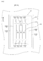
- FIG. 1 is a plan view of a wired circuit board as one embodiment of the present invention.
- FIG. 2 is a cross-sectional view of the printed circuit board shown in FIG. 1 taken along the line AA.
- 3A and 3B are explanatory diagrams for explaining the method of manufacturing the printed circuit board.
- FIG. 3A shows a step (first step) of setting a pattern forming region and an opening forming region on a support layer.
- FIG. 3B shows a step (second step) of forming a base insulating layer in the pattern forming region and forming a dummy insulating layer in the opening forming region, subsequent to FIG. 3A.
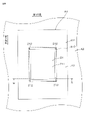
- FIG. 4 is a plan view of the support layer, base insulating layer and dummy insulating layer shown in FIG. 3B.
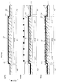
- FIG. 3B is a BB cross-sectional view of the supporting layer, base insulating layer and dummy insulating layer shown in FIG. 5A to 5C are explanatory diagrams for explaining the method for manufacturing the printed circuit board following FIG. 3B.
- FIG. 5A shows a step of forming a seed layer on the base insulating layer and the dummy insulating layer following FIG. 3B.
- FIG. 5B shows a step of bonding a plating resist onto the base insulating layer and the dummy insulating layer on which the seed layer is formed and exposing, subsequent to FIG. 5A.
- FIG. 5C shows the step of developing the exposed plating resist following FIG. 5B.
- 6A to 6C are explanatory diagrams for explaining the method of manufacturing the printed circuit board following FIG.
- FIG. 6A shows a step (third step) of forming conductor patterns and dummy patterns by electrolytic plating subsequent to FIG. 5C.
- FIG. 6B shows a step of removing the plating resist following FIG. 6A.
- FIG. 6C shows a step of removing the seed layer covered with the plating resist by etching, following FIG. 6B.
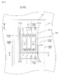
- FIG. 7 is a plan view of the support layer, base insulating layer, dummy insulating layer, conductor pattern and dummy pattern shown in FIG. 6C.
- 6C is a CC sectional view of the support layer, base insulating layer, dummy insulating layer, conductor pattern and dummy pattern shown in FIG. 7.
- FIG. 7 is a plan view of the support layer, base insulating layer, dummy insulating layer, conductor pattern and dummy pattern shown in FIG. 7.
- FIG. 7 is a plan view of the support layer, base insulating layer, dummy insulating layer, conductor pattern and
- FIG. 8A and 8B are explanatory diagrams for explaining the method for manufacturing the printed circuit board following FIG. 6C.
- FIG. 8A shows a step of forming an insulating cover layer subsequent to FIG. 6C.
- FIG. 8B shows the step of etching the support layer (fourth step) subsequent to FIG. 8A.
- 9A to 9C are explanatory diagrams for explaining modification (1).
- FIG. 9A shows a step (second step) of forming a base insulating layer in the pattern forming region and not forming the dummy insulating layer in the opening forming region.
- FIG. 9B shows a step (third step) of forming a dummy pattern on the support layer in the opening forming region, following FIG. 9A.
- FIG. 9A shows a step of forming an insulating cover layer subsequent to FIG. 6C.
- FIG. 8B shows the step of etching the support layer (fourth step) subsequent to FIG. 8A.
- 9A to 9C are explan
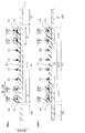
- FIG. 9C shows the step of etching the support layer (fourth step) subsequent to FIG. 9B.
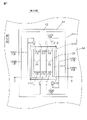
- FIG. 10 is a plan view of the support layer, base insulating layer, dummy insulating layer, conductor pattern and dummy pattern shown in FIG. 9C.
- 9C is a DD cross-sectional view of the support layer, base insulating layer, dummy insulating layer, conductor pattern, and dummy pattern shown in FIG.
- FIG. 11 is an explanatory diagram for explaining modification (3), in which in the third step, a dummy pattern is formed on the support layer at the periphery of the opening forming region, and a dummy pattern is formed at the central portion of the opening forming region. indicates the case where the dummy pattern 22 is not formed.
- FIG. 12 is an explanatory diagram for explaining the modification (3) together with FIG. 11, and shows a case where dummy patterns are formed on the support layer over the entire opening formation region in the third step.
- a wired circuit board 1 extends in a first direction and a second direction.
- the printed circuit board 1 has a substantially rectangular shape. Note that the shape of the printed circuit board 1 is not limited.
- the printed circuit board 1 has an opening 10 .
- the opening 10 is arranged at the center of the wired circuit board 1 in the first direction and at the center of the wired circuit board 1 in the second direction. Opening 10 extends in a first direction and a second direction.
- the opening 10 has a substantially rectangular shape. The position of the opening 10 in the printed circuit board 1 and the shape of the opening 10 are not limited.
- the wired circuit board 1 has a support layer 11, a base insulating layer 12 as an example of an insulating layer, a conductive pattern 13, and an insulating cover layer .
- the support layer 11 supports the insulating base layer 12, the conductor pattern 13, and the insulating cover layer .
- the support layer 11 is made of metal foil. Examples of metals include stainless alloys and copper alloys.
- the insulating base layer 12 is arranged on the support layer 11 in the thickness direction of the printed circuit board 1 .
- the thickness direction is orthogonal to the first direction and the second direction.
- the insulating base layer 12 is arranged between the support layer 11 and the conductive pattern 13 in the thickness direction.
- the insulating base layer 12 insulates the support layer 11 and the conductor pattern 13 .
- the insulating base layer 12 is made of resin. Examples of resin include polyimide.
- the conductor pattern 13 is arranged on the base insulating layer 12 in the thickness direction.
- the conductive pattern 13 is arranged on the side opposite to the supporting layer 11 with respect to the insulating base layer 12 in the thickness direction.
- a conductor pattern 13 is arranged around the opening 10 .
- the conductor pattern 13 is made of metal. Examples of metals include copper.
- the shape of the conductor pattern 13 is not limited.
- the conductor pattern 13 includes a plurality of terminals 131A, 131B, 131C and 131D, a plurality of terminals 132A, 132B, 132C and 132D, a plurality of wirings 133A, 133B, 133C, 133D. Note that the number of terminals and the number of wirings are not limited.
- terminals 131A, 131B, 131C, and 131D are arranged at one end of the printed circuit board 1 in the second direction.
- Terminals 131A, 131B, 131C, and 131D are arranged on one side of opening 10 in the second direction.
- the terminals 131A, 131B, 131C, and 131D are arranged in the first direction at intervals.
- Each of terminals 131A, 131B, 131C, and 131D has a square land shape.
- terminals 132A, 132B, 132C, and 132D are arranged at the other end of the printed circuit board 1 in the second direction.
- Terminals 131A, 131B, 131C, and 131D are arranged on the other side with respect to opening 10 in the second direction.
- Terminals 132A, 132B, 132C, and 132D are arranged in the first direction at intervals.
- Each of terminals 132A, 132B, 132C, and 132D has a square land shape.
- (1-3-2) Wiring One end of the wiring 133A is connected to the terminal 131A.
- the other end of the wiring 133A is connected to the terminal 132A.
- the wiring 133A electrically connects the terminals 131A and 132A.
- One end of the wiring 133B is connected to the terminal 131B.
- the other end of the wiring 133B is connected to the terminal 132B.
- the wiring 133B electrically connects the terminals 131B and 132B.
- One end of the wiring 133C is connected to the terminal 131C.
- the other end of the wiring 133C is connected to the terminal 132C.
- the wiring 133C electrically connects the terminals 131C and 132C.
- One end of the wiring 133D is connected to the terminal 131D.
- the other end of the wiring 133D is connected to the terminal 132D.
- the wiring 133D electrically connects the terminal 131D and the terminal 132D.
- each of the plurality of terminals 131A, 131B, 131C, and 131D is referred to as a terminal 131
- each of the plurality of terminals 132A, 132B, 132C, and 132D is referred to as a terminal 132
- a plurality of wirings Each of 133A, 133B, 133C, and 133D is described as wiring 133 .
- the cover insulating layer 14 covers all the wirings 133 .
- the insulating cover layer 14 is arranged on the insulating base layer 12 in the thickness direction. Note that the insulating cover layer 14 does not cover the terminals 131 and 132 .
- the insulating cover layer 14 is made of resin. Examples of resins include polyimide.
- the printed circuit board 1 is manufactured by a semi-additive method.
- the printed circuit board 1 may be manufactured by an additive method.
- the method for manufacturing the printed circuit board 1 includes a first step (see FIG. 3A), a second step (see FIG. 3B), a third step (see FIGS. 5A to 6C), and a fourth step (see FIG. 8B). and a fifth step (see FIGS. 8B and 2).
- the support layer 11 is provided with a product region A1 and a frame region A2.
- the support layer 11 is a metal foil drawn from a roll of metal foil.
- the wired circuit board 1 described above is manufactured in the product area A1.
- the product area A1 includes a pattern formation area A11 and an opening formation area A12.
- the pattern forming region A11 and the opening forming region A12 are set in the support layer.
- the pattern formation area A11 is arranged outside the opening formation area A12.
- the pattern formation area A11 surrounds the opening formation area A12.
- the insulating base layer 12, the conductive pattern 13 and the insulating cover layer 14 described above are formed in the pattern forming region A11.
- the opening 10 described above is formed in the opening forming region A12.
- the frame area A2 is set outside the product area A1.
- the frame area A2 is connected with the product area A1.
- a frame for supporting the printed circuit board 1 is formed in the frame area A2.
- an insulating layer is formed on the support layer 11 at least in the pattern formation region A11.
- an insulating layer is formed in the pattern formation region A11 and the opening formation region A12.
- the base insulating layer 12 described above is formed in the pattern forming region A11, and the dummy insulating layer 21 is formed in the opening forming region A12.
- the dummy insulating layer 21 supports the dummy pattern 22 (see FIG. 7).
- the dummy pattern 22 will be explained later.
- the dummy insulating layer 21 has a support portion 211 and at least one connection portion 212 .
- the dummy insulating layer 21 has a plurality of connection portions 212 .
- the supporting portion 211 supports the dummy pattern 22 .
- the support part 211 is arranged apart from the base insulating layer 12 .
- the support portion 211 has a substantially rectangular shape. Note that the shape of the support portion 211 is not limited.
- Each of the plurality of connecting portions 212 is arranged between the supporting portion 211 and the insulating base layer 12 .
- Each of the plurality of connecting portions 212 is connected to the supporting portion 211 and the insulating base layer 12 .
- the dummy insulating layer 21 is thereby connected to the base insulating layer 12 .
- a photosensitive resin solution (varnish) is applied onto the support layer 11 and dried to form a photosensitive resin coating film.
- the photosensitive resin coating is exposed and developed. Thereby, the base insulating layer 12 and the dummy insulating layer 21 are formed on the support layer 11 .
- the conductive pattern 13 is formed on the base insulating layer 12 in the pattern forming region A11 by electrolytic plating, A dummy pattern 22 is formed on the dummy insulating layer 21 in the opening forming region A12.
- a seed layer 23 is formed on the surfaces of the base insulating layer 12 and the dummy insulating layer 21 .
- the seed layer 23 is formed by sputtering, for example. Examples of materials for the seed layer 23 include chromium, copper, nickel, titanium, and alloys thereof.
- a plating resist R is adhered onto the base insulating layer 12 and the dummy insulating layer 21 on which the seed layer 23 is formed, and the conductor pattern 13 (see FIG. 7) and the dummy pattern 22 are formed. (See FIG. 7), the plating resist R is exposed while shielding the light.
- the exposed plating resist R is developed. Then, the plating resist R in the light-shielded portion is removed, and the seed layer 23 is exposed in the portion where the conductor pattern 13 and the dummy pattern 22 are to be formed. The plating resist R remains in the exposed portion, that is, the portion where the conductor pattern 13 and the dummy pattern 22 are not formed.
- conductive patterns 13 and dummy patterns 22 are formed on the exposed seed layer 23 by electroplating.
- the conductor pattern 13 is formed together with the dummy pattern 22 . Therefore, in the plating solution, the metal ion concentration around the product area A1 can be made uniform, and the thickness of the conductor pattern 13 can be made uniform.
- the plating resist R is peeled off after the electrolytic plating is finished.
- the seed layer 23 covered with the plating resist R is removed by etching.
- the conductor pattern 13 is formed on the base insulating layer 12, and the dummy pattern 22 is formed on the dummy insulating layer 21, as shown in FIG.
- the insulating cover layer 14 is formed on the insulating base layer 12 and the conductor pattern 13 in the same manner as the insulating base layer 12 is formed.
- the cover insulating layer 14 is not formed on the dummy insulating layer 21 and the dummy pattern 22 in this embodiment, the cover insulating layer 14 may be formed on the dummy insulating layer 21 and the dummy pattern 22. .
- the entire support layer 11 in the opening formation region A12 is etched to form the openings 10 in the support layer 11 .
- the supporting layer 11 between the product area A1 and the frame area A2 is etched to form the outer shape of the wired circuit board 1 along the shape of the product area A1 and the shape of the frame area A2. form a frame F along .
- the portions of the support layer 11 that are not to be etched are covered with an etching resist, and the support layer 11 is immersed in an etchant.
- the entire support layer 11 within the opening forming region A12 is etched, and the opening 10 is formed.
- the dummy pattern 22 is supported by the dummy insulating layer 21, even if the entire support layer 11 within the opening forming region A12 is etched, the dummy pattern 22 will not come off into the etchant. Therefore, the dummy pattern 22 can be provided in the opening formation region A12 without a device for recovering the dummy pattern 22 dropped into the etchant.
- the method of cutting the wired circuit board 1 from the frame F and the method of cutting the dummy insulating layer 21 from the wired circuit board 1 are not limited.
- the wired circuit board 1 is cut out from the frame F, and the dummy insulating layer 21 is cut out from the wired circuit board 1 .
- Traces of cutting the dummy insulating layer 21 may remain on the inner surface of the opening 10 of the wired circuit board 1 .
- the conductor pattern 13 in the pattern forming area A11 can be formed together with the dummy pattern 22 in the opening forming area A12.
- the concentration of metal ions around the conductor pattern 13 can be made uniform in the plating solution.
- the thickness of the conductor pattern 13 formed near the opening 10 can be made uniform.
- the dummy pattern 22 can be supported by the dummy insulating layer 21 in the opening forming region A12, as shown in FIG. 8B.
- the dummy pattern 22 can be supported by the dummy insulating layer 21 even if the support layer 11 in the opening formation region A12 is entirely etched.
- the support layer 11 in the opening forming area A12 is entirely etched to form the opening 10, and the product area A1 and the frame area A2 are formed.
- the support layer 11 between them By etching the support layer 11 between them, the outline of the wired circuit board 1 is formed, and the frame F connected to the wired circuit board 1 is formed.
- the wired circuit board 1 is cut out from the frame F, and the dummy insulating layer 21 in the opening 10 is cut out from the wired circuit board 1 .
- FIG. 9A to 10 members similar to those of the embodiment described above are denoted by the same reference numerals, and descriptions thereof are omitted.
- the base insulating layer 12 may be formed in the pattern forming region A11 and the dummy insulating layer 21 may not be formed in the opening forming region A12.
- dummy patterns 22 are formed on the support layer 11 in the opening forming region A12 in the third step.
- part of the support layer 11 within the opening forming region A12 is etched. Specifically, a part of the support layer 11 in the opening forming area A12 is etched along the boundary between the pattern forming area A11 and the opening forming area A12. As a result, the dummy supporting layer 31 that supports the dummy pattern 22 is formed in the opening formation region A12.
- the dummy support layer 31 is composed of the support layer 11 and has the same shape as the dummy insulating layer 21 described above. Specifically, the dummy support layer 31 has a support portion 311 and at least one connection portion 312 . In this modification, the dummy support layer 31 has a plurality of connecting portions 312 .
- the supporting portion 311 supports the dummy pattern 22 .
- the support portion 311 is arranged apart from the base insulating layer 12 .
- the support portion 311 has a substantially rectangular shape. Note that the shape of the support portion 311 is not limited.
- Each of the plurality of connecting portions 312 is arranged between the supporting portion 311 and the insulating base layer 12 .
- Each of the plurality of connection portions 312 is connected to the support portion 311 and the support layer 11 under the base insulating layer 12 .
- the dummy support layer 31 is connected to the support layer 11 under the base insulating layer 12 .
- the dummy support layer 31 is cut out from the printed circuit board 1 in the fifth step.
- part of the support layer 11 in the opening forming region A12 is etched in the same manner as in the modified example (1) described above to form the dummy insulating layer 21.
- a dummy support layer 31 (see FIG. 9C) having the same shape may be formed.
- the dummy support layer 31 may not be formed, and the entire support layer 11 within the opening formation region A12 may be etched.
- the base insulating layer 12 is formed within the pattern forming region A11, and the dummy insulating layer 21 is not formed within the opening forming region A12.
- dummy patterns 22 are formed on the support layer 11 in the opening forming region A12.
- the dummy pattern 22 is formed in the peripheral portion A121 of the opening forming region A12, and the dummy pattern 22 is not formed in the central portion A122 of the opening forming region A12.
- the peripheral portion A121 is a portion located between the central portion A122 and the conductor pattern 13 .
- the dummy pattern 22 is formed over the entire opening forming area A12.
- the entire support layer 11 within the opening forming region A12 is etched.
- the dummy pattern 22 may drop into the etchant.
- the dummy pattern 22 can be easily removed by etching the entire support layer 11 within the opening forming region A12.
- the dummy pattern 22 may be formed in the peripheral edge portion A121 of the opening forming region A12, and the dummy pattern 22 may not be formed in the central portion A122 of the opening forming region A12. can.
- the dummy pattern 22 may be formed not only in the opening forming area A12 but also in the frame area A2. It should be noted that although the above invention has been provided as an exemplary embodiment of the present invention, this is merely an illustration and should not be construed as a limitation. Variations of the invention that are obvious to those skilled in the art are included in the following claims.
- the method for manufacturing a wired circuit board of the present invention is used for manufacturing a wired circuit board.
Landscapes
- Engineering & Computer Science (AREA)
- Chemical & Material Sciences (AREA)
- Manufacturing & Machinery (AREA)
- Microelectronics & Electronic Packaging (AREA)
- Chemical Kinetics & Catalysis (AREA)
- Electrochemistry (AREA)
- Materials Engineering (AREA)
- Metallurgy (AREA)
- Organic Chemistry (AREA)
- General Chemical & Material Sciences (AREA)
- Structure Of Printed Boards (AREA)
- Manufacturing Of Printed Wiring (AREA)
Abstract
Description
図1に示すように、配線回路基板1は、第1方向および第2方向に延びる。本実施形態では、配線回路基板1は、略矩形状を有する。なお、配線回路基板1の形状は、限定されない。配線回路基板1は、開口10を有する。
支持層11は、ベース絶縁層12、導体パターン13、および、カバー絶縁層14を支持する。本実施形態では、支持層11は、金属箔からなる。金属として、例えば、ステンレス合金、および、銅合金が挙げられる。
ベース絶縁層12は、配線回路基板1の厚み方向において、支持層11の上に配置される。厚み方向は、第1方向および第2方向と直交する。ベース絶縁層12は、厚み方向において、支持層11と導体パターン13との間に配置される。ベース絶縁層12は、支持層11と導体パターン13とを絶縁する。ベース絶縁層12は、樹脂からなる。樹脂として、例えば、ポリイミドが挙げられる。
導体パターン13は、厚み方向において、ベース絶縁層12の上に配置される。導体パターン13は、厚み方向において、ベース絶縁層12に対して、支持層11の反対側に配置される。導体パターン13は、開口10の周りに配置される。導体パターン13は、金属からなる。金属として、例えば、銅が挙げられる。導体パターン13の形状は、限定されない。
本実施形態では、端子131A,131B,131C,131Dは、第2方向における配線回路基板1の一端部に配置される。端子131A,131B,131C,131Dは、第2方向において、開口10に対して一方側に配置される。端子131A,131B,131C,131Dは、互いに間隔を隔てて、第1方向に並ぶ。端子131A,131B,131C,131Dのそれぞれは、角ランド形状を有する。
配線133Aの一端は、端子131Aと接続する。配線133Aの他端は、端子132Aと接続する。配線133Aは、端子131Aと端子132Aとを電気的に接続する。
図1に示すように、カバー絶縁層14は、全ての配線133を覆う。カバー絶縁層14は、厚み方向において、ベース絶縁層12の上に配置される。なお、カバー絶縁層14は、端子131および端子132を覆わない。カバー絶縁層14は、樹脂からなる。樹脂としては、例えば、ポリイミドが挙げられる。
次に、配線回路基板1の製造方法について説明する。
図3Aに示すように、第1工程では、支持層11に、製品領域A1とフレーム領域A2とを設定する。本実施形態では、支持層11は、金属箔のロールから引き出された金属箔である。
次に、図3Bに示すように、第2工程では、少なくともパターン形成領域A11内において、支持層11の上に絶縁層を形成する。本実施形態では、パターン形成領域A11内および開口形成領域A12内に絶縁層を形成する。
次に、図5Aから図6Cに示すように、第3工程では、電解メッキにより、パターン形成領域A11内のベース絶縁層12の上に、導体パターン13を形成するとともに、開口形成領域A12内のダミー絶縁層21の上にダミーパターン22を形成する。
次に、図8Bに示すように、第4工程では、開口形成領域A12内の支持層11の全部をエッチングして、支持層11に開口10を形成する。また、第4工程において、製品領域A1とフレーム領域A2との間の支持層11をエッチングして、製品領域A1の形状に沿って配線回路基板1の外形を形成するとともに、フレーム領域A2の形状に沿ってフレームFを形成する。
次に、図2に示すように、第5工程では、配線回路基板1をフレームFから切り取るとともに、開口10内のダミー絶縁層21を、配線回路基板1から切り取る。
(1)配線回路基板1の製造方法によれば、図6Cおよび図7に示すように、電解メッキにより、パターン形成領域A11内のベース絶縁層12の上に導体パターン13を形成するとともに、開口形成領域A12内のダミー絶縁層21の上にダミーパターン22を形成する。
次に、図9Aから図10を参照して、変形例について説明する。変形例において、上記した実施形態と同様の部材には同じ符号を付し、説明を省略する。
なお、上記発明は、本発明の例示の実施形態として提供したが、これは単なる例示に過ぎず、限定的に解釈してはならない。当該技術分野の当業者によって明らかな本発明の変形例は、後記請求の範囲に含まれる。
10 開口
11 支持層
12 ベース絶縁層
13 導体パターン
21 ダミー絶縁層
22 ダミーパターン
31 ダミー支持層
A1 製品領域
A2 フレーム領域
A11 パターン形成領域
A12 開口形成領域
F フレーム
Claims (5)
- 支持層にパターン形成領域と開口形成領域とを設定する第1工程と、
少なくとも前記パターン形成領域内において、前記支持層の上に絶縁層を形成する第2工程と、
電解メッキにより、前記パターン形成領域内の前記絶縁層の上に導体パターンを形成するとともに、前記開口形成領域内にダミーパターンを形成する第3工程と、
前記開口形成領域内の前記支持層の少なくとも一部をエッチングする第4工程と
を含む、配線回路基板の製造方法。 - 前記第2工程において、前記パターン形成領域内および前記開口形成領域内に前記絶縁層を形成し、
前記第3工程において、前記開口形成領域内の前記絶縁層の上に前記ダミーパターンを形成する、請求項1に記載の配線回路基板の製造方法。 - 前記第1工程において、前記支持層に、前記パターン形成領域と前記開口形成領域とを含む製品領域と、前記製品領域と接続されるフレーム領域とを、さらに設定し、
前記第4工程において、前記開口形成領域内の前記支持層の全部をエッチングして、前記支持層に開口を形成し、前記製品領域と前記フレーム領域との間の前記支持層の一部をエッチングして、前記製品領域の形状に沿って配線回路基板の外形を形成するとともに、前記フレーム領域の形状に沿って、前記配線回路基板と接続されるフレームを形成し、
前記配線回路基板の製造方法は、
前記配線回路基板を前記フレームから切り取るとともに、前記開口内の前記絶縁層を、前記配線回路基板から切り取る第5工程を、さらに含む、請求項2に記載の配線回路基板の製造方法。 - 前記第2工程において、前記パターン形成領域内に前記絶縁層を形成し、前記開口形成領域内に前記絶縁層を形成せず、
前記第3工程において、前記開口形成領域内の前記支持層の上に前記ダミーパターンを形成する、請求項1に記載の配線回路基板の製造方法。 - 前記第4工程において、前記開口形成領域内の前記支持層の全部をエッチングする、請求項4に記載の配線回路基板の製造方法。
Priority Applications (2)
| Application Number | Priority Date | Filing Date | Title |
|---|---|---|---|
| US18/569,093 US20240284600A1 (en) | 2021-06-14 | 2022-05-24 | Method for producing wiring circuit board |
| CN202280041269.7A CN117461394A (zh) | 2021-06-14 | 2022-05-24 | 布线电路基板的制造方法 |
Applications Claiming Priority (4)
| Application Number | Priority Date | Filing Date | Title |
|---|---|---|---|
| JP2021-098999 | 2021-06-14 | ||
| JP2021098999 | 2021-06-14 | ||
| JP2022062685A JP2022190665A (ja) | 2021-06-14 | 2022-04-04 | 配線回路基板の製造方法 |
| JP2022-062685 | 2022-04-04 |
Publications (1)
| Publication Number | Publication Date |
|---|---|
| WO2022264756A1 true WO2022264756A1 (ja) | 2022-12-22 |
Family
ID=84526162
Family Applications (1)
| Application Number | Title | Priority Date | Filing Date |
|---|---|---|---|
| PCT/JP2022/021222 Ceased WO2022264756A1 (ja) | 2021-06-14 | 2022-05-24 | 配線回路基板の製造方法 |
Country Status (3)
| Country | Link |
|---|---|
| US (1) | US20240284600A1 (ja) |
| TW (1) | TW202306451A (ja) |
| WO (1) | WO2022264756A1 (ja) |
Families Citing this family (1)
| Publication number | Priority date | Publication date | Assignee | Title |
|---|---|---|---|---|
| JP2024168241A (ja) * | 2023-05-23 | 2024-12-05 | 日東電工株式会社 | 配線回路基板、および、配線回路基板の製造方法 |
Citations (4)
| Publication number | Priority date | Publication date | Assignee | Title |
|---|---|---|---|---|
| JP2003273498A (ja) * | 2002-03-12 | 2003-09-26 | Nitto Denko Corp | プリント配線板の製造方法 |
| JP2010147251A (ja) * | 2008-12-18 | 2010-07-01 | Nitto Denko Corp | 配線回路基板集合体シート |
| JP2012038914A (ja) * | 2010-08-06 | 2012-02-23 | Nitto Denko Corp | 配線回路基板集合体シートおよびその製造方法 |
| JP2021050389A (ja) * | 2019-09-25 | 2021-04-01 | 大日本印刷株式会社 | 配線基板および配線基板の製造方法 |
-
2022
- 2022-05-24 WO PCT/JP2022/021222 patent/WO2022264756A1/ja not_active Ceased
- 2022-05-24 US US18/569,093 patent/US20240284600A1/en active Pending
- 2022-06-02 TW TW111120576A patent/TW202306451A/zh unknown
Patent Citations (4)
| Publication number | Priority date | Publication date | Assignee | Title |
|---|---|---|---|---|
| JP2003273498A (ja) * | 2002-03-12 | 2003-09-26 | Nitto Denko Corp | プリント配線板の製造方法 |
| JP2010147251A (ja) * | 2008-12-18 | 2010-07-01 | Nitto Denko Corp | 配線回路基板集合体シート |
| JP2012038914A (ja) * | 2010-08-06 | 2012-02-23 | Nitto Denko Corp | 配線回路基板集合体シートおよびその製造方法 |
| JP2021050389A (ja) * | 2019-09-25 | 2021-04-01 | 大日本印刷株式会社 | 配線基板および配線基板の製造方法 |
Also Published As
| Publication number | Publication date |
|---|---|
| US20240284600A1 (en) | 2024-08-22 |
| TW202306451A (zh) | 2023-02-01 |
Similar Documents
| Publication | Publication Date | Title |
|---|---|---|
| JP4523051B2 (ja) | 配線回路基板の製造方法 | |
| JP2011049316A (ja) | 配線回路基板およびその製造方法 | |
| US8377317B2 (en) | Method for manufacturing printed circuit board with thick traces | |
| WO2022264756A1 (ja) | 配線回路基板の製造方法 | |
| JP2022190665A (ja) | 配線回路基板の製造方法 | |
| US12563675B2 (en) | Wiring circuit board assembly sheet | |
| JP6027819B2 (ja) | 配線回路基板 | |
| JP5513637B2 (ja) | 配線回路基板の製造方法 | |
| JP2024072219A (ja) | 配線回路基板の製造方法、ダミーパターン付き配線回路基板、および、集合体シート | |
| CN117461394A (zh) | 布线电路基板的制造方法 | |
| JP2024072216A (ja) | 配線回路基板 | |
| JP7203939B2 (ja) | 配線回路基板の製造方法 | |
| US20240237200A1 (en) | Assembly sheet and method for producing assembly sheet | |
| JP2025088473A (ja) | 配線回路基板、および、配線回路基板の製造方法 | |
| JP2025173250A (ja) | 配線回路基板付きシートの製造方法、および、配線回路基板付きシート | |
| JP2024046953A (ja) | 配線回路基板の製造方法、および、配線回路基板 | |
| JP2024046954A (ja) | 配線回路基板の製造方法 | |
| JP2024046956A (ja) | 配線回路基板 | |
| JP2024046955A (ja) | 配線回路基板の製造方法、および、配線回路基板 | |
| JP4566760B2 (ja) | 配線回路基板の製造方法 | |
| JP2025154909A (ja) | 配線回路基板の製造方法 | |
| JP2025168110A (ja) | 配線回路基板、および、配線回路基板の製造方法 | |
| JP2025118402A (ja) | 集合体シート、および、集合体シートの製造方法 | |
| JP5513638B2 (ja) | 配線回路基板 | |
| JP2000049195A (ja) | 電子部品用部材の製造方法 |
Legal Events
| Date | Code | Title | Description |
|---|---|---|---|
| 121 | Ep: the epo has been informed by wipo that ep was designated in this application |
Ref document number: 22824750 Country of ref document: EP Kind code of ref document: A1 |
|
| WWE | Wipo information: entry into national phase |
Ref document number: 202280041269.7 Country of ref document: CN |
|
| WWE | Wipo information: entry into national phase |
Ref document number: 18569093 Country of ref document: US |
|
| NENP | Non-entry into the national phase |
Ref country code: DE |
|
| 122 | Ep: pct application non-entry in european phase |
Ref document number: 22824750 Country of ref document: EP Kind code of ref document: A1 |