WO2022259986A1 - 発光装置 - Google Patents
発光装置 Download PDFInfo
- Publication number
- WO2022259986A1 WO2022259986A1 PCT/JP2022/022691 JP2022022691W WO2022259986A1 WO 2022259986 A1 WO2022259986 A1 WO 2022259986A1 JP 2022022691 W JP2022022691 W JP 2022022691W WO 2022259986 A1 WO2022259986 A1 WO 2022259986A1
- Authority
- WO
- WIPO (PCT)
- Prior art keywords
- lens
- center position
- light
- emitting device
- distance
- Prior art date
- Legal status (The legal status is an assumption and is not a legal conclusion. Google has not performed a legal analysis and makes no representation as to the accuracy of the status listed.)
- Ceased
Links
Images


Classifications
-
- H—ELECTRICITY
- H01—ELECTRIC ELEMENTS
- H01S—DEVICES USING THE PROCESS OF LIGHT AMPLIFICATION BY STIMULATED EMISSION OF RADIATION [LASER] TO AMPLIFY OR GENERATE LIGHT; DEVICES USING STIMULATED EMISSION OF ELECTROMAGNETIC RADIATION IN WAVE RANGES OTHER THAN OPTICAL
- H01S5/00—Semiconductor lasers
- H01S5/02—Structural details or components not essential to laser action
- H01S5/022—Mountings; Housings
- H01S5/0225—Out-coupling of light
- H01S5/02253—Out-coupling of light using lenses
-
- H—ELECTRICITY
- H01—ELECTRIC ELEMENTS
- H01S—DEVICES USING THE PROCESS OF LIGHT AMPLIFICATION BY STIMULATED EMISSION OF RADIATION [LASER] TO AMPLIFY OR GENERATE LIGHT; DEVICES USING STIMULATED EMISSION OF ELECTROMAGNETIC RADIATION IN WAVE RANGES OTHER THAN OPTICAL
- H01S5/00—Semiconductor lasers
- H01S5/02—Structural details or components not essential to laser action
- H01S5/022—Mountings; Housings
- H01S5/0225—Out-coupling of light
- H01S5/02255—Out-coupling of light using beam deflecting elements
Definitions
- the present disclosure relates to a light emitting device.
- Patent Document 1 a light-emitting device equipped with a plurality of semiconductor laser packages is known (for example, Patent Document 1).
- the light-emitting device described in Patent Document 1 includes a plurality of CAN packages mounted on a mounting substrate, and attempts to collect laser light from the plurality of CAN packages by a lens array.
- Each of the plurality of CAN packages has a semiconductor laser chip.
- Light emitting devices are required to have higher output, and the current supplied to each semiconductor laser chip tends to increase. As a result, the amount of heat generated in each semiconductor laser chip increases, so it is necessary to secure a heat radiation path from each semiconductor laser chip.
- An object of the present disclosure is to solve such problems, and to provide a light-emitting device that can improve the heat dissipation characteristics of a semiconductor laser chip.
- one aspect of the light emitting device includes a base having a main surface, and a plurality of semiconductor laser chips mounted on the main surface and having optical axes parallel to the main surface. , a plurality of mirrors, each having a reflecting surface for reflecting light emitted from the emission point of each of the plurality of semiconductor laser chips; and a plurality of mirrors, each receiving the reflected light from the reflecting surface of each of the plurality of mirrors. from the center position of the emitted light on the reflecting surface to the center position of the lens portion corresponding to the reflecting surface among the plurality of lens portions in a plan view of the main surface.
- the output light from each of the plurality of lens portions having the larger first distance from the lens portion located on the outermost side of the lens region among the lens portions is inside a predetermined surface region having an area smaller than that of the lens region. is irradiated to
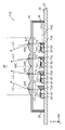
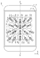
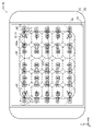
- FIG. 1 is a plan view of a light emitting device according to Embodiment 1.
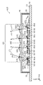
- FIG. 2 is a cross-sectional view of the light-emitting device according to Embodiment 1.
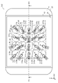
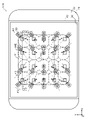
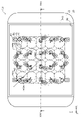
- FIG. 3 is a plan view of the light-emitting device according to Embodiment 1 from which the optical members are removed.
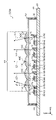
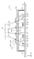
- 4 is a cross-sectional view showing configurations of a semiconductor laser chip, a submount, and a mirror according to Embodiment 1.
- FIG. 5 is a cross-sectional view illustrating optical paths in the light-emitting device according to Embodiment 1.
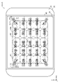
- FIG. 6 is a diagram showing a positional relationship between a plurality of mirrors and a plurality of lens units in the light emitting device according to Embodiment 1.
- FIG. 1 is a plan view of a light emitting device according to Embodiment 1.
- FIG. 2 is a cross-sectional view of the light-emitting device according to Embodiment 1.
- FIG. 3 is
- FIG. 7 is a cross-sectional view of a light-emitting device according to Modification 1 of Embodiment 1.
- FIG. 8 is a cross-sectional view of a light-emitting device according to Modification 2 of Embodiment 1.
- FIG. 9 is a plan view showing a state in which the optical member of the light emitting device according to Embodiment 2 is removed.
- 10 is a cross-sectional view of a light-emitting device according to Embodiment 2.
- FIG. 11 is a cross-sectional view of a light-emitting device according to a modification of Embodiment 2.
- FIG. 12 is a plan view showing a state in which the optical member of the light-emitting device according to Embodiment 3 is removed.
- FIG. 13 is a cross-sectional view of a light-emitting device according to Embodiment 3.
- FIG. 14 is a cross-sectional view of a light-emitting device according to a modification of Embodiment 3.
- FIG. 15 is a plan view showing a state in which the optical members are removed from the light-emitting device according to Embodiment 4.
- FIG. 16 is a cross-sectional view of a light-emitting device according to Embodiment 4.
- FIG. 17 is a cross-sectional view of a light-emitting device according to a modification of Embodiment 4.
- FIG. 18 is a plan view of the light-emitting device according to Embodiment 5 from which the optical member is removed.
- FIG. 19 is a cross-sectional view of a light-emitting device according to Embodiment 5.
- FIG. FIG. 20 is a plan view showing a state in which the optical member of the light-emitting device according to Embodiment 6 is removed.
- 21 is a plan view showing a state in which an optical member is removed from a light-emitting device according to a modification of Embodiment 6.
- FIG. 22 is a plan view showing a state in which the optical members of the light emitting device according to Embodiment 7 are removed.
- FIG. 23 is a plan view showing a state in which an optical member is removed from a light-emitting device according to a modification of Embodiment 7.
- FIG. 24 is a plan view showing a state in which the optical member of the light-emitting device according to Embodiment 8 is removed.
- 25 is a schematic cross-sectional view of a light-emitting device according to Embodiment 8.
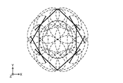
- FIG. 26 is a diagram showing a far-field image in which all output light profiles in a predetermined surface area of the light-emitting device according to Embodiment 8 are superimposed.
- 27 is a schematic cross-sectional view of a light-emitting device according to a modification of Embodiment 8.
- each figure is a schematic diagram and is not necessarily strictly illustrated. Therefore, the scales and the like are not always the same in each drawing.
- symbol is attached
- the terms “upper” and “lower” do not refer to the upward direction (vertically upward) and the downward direction (vertically downward) in absolute spatial recognition, but are based on the stacking order in the stacking structure. It is used as a term defined by a relative positional relationship. Also, the terms “above” and “below” are used not only when two components are spaced apart from each other and there is another component between the two components, but also when two components are spaced apart from each other. It also applies when they are arranged in contact with each other.
- Embodiment 1 A light-emitting device according to Embodiment 1 will be described.
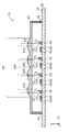
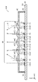
- FIG. 1 and 2 are respectively a plan view and a cross-sectional view of a light emitting device 10 according to this embodiment.
- FIG. 2 shows a cross section taken along line II-II of FIG.
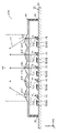
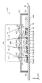
- FIG. 3 is a plan view showing a state in which the optical member 40 is removed from the light emitting device 10 according to this embodiment.
- Each figure also shows an X-axis, a Y-axis, and a Z-axis that are orthogonal to each other.
- the light-emitting device 10 is a device that irradiates light onto a predetermined surface area (not shown) located away from the light-emitting device 10 in the Z direction. 20 , a plurality of semiconductor laser chips 60 , a plurality of mirrors 70 and an optical member 40 .
- light emitting device 10 further includes frame member 30 and a plurality of submounts 50 .
- the base 20 shown in FIGS. 1 to 3 is a member having a main surface 21 on which a plurality of semiconductor laser chips 60 are mounted.
- the base 20 is a substrate having a substantially rectangular plate-like shape.
- the base 20 is made of a material with high thermal conductivity, and also functions as a heat dissipation member that dissipates the heat generated by the plurality of semiconductor laser chips 60 .
- the material of the base 20 is, for example, a metal material, a ceramic material, a glass material, a resin material, or the like.
- the base 20 is preferably made of a material with high thermal conductivity such as a metal material. Examples of metal materials that have high thermal conductivity and are practical for the base 20 include Cu and Al.
- the base 20 is a Cu substrate made of Cu.
- a structure for fixing the base 20 may be formed on a portion of the base 20 outside the frame member 30 or the like.
- a through hole or the like may be formed in the base 20 .
- the frame member 30 shown in FIGS. 2 and 3 is an annular member surrounding multiple semiconductor laser chips 60 and multiple mirrors 70 .
- the frame member 30 is erected on the main surface 21 of the base 20 and functions as a part of a container that houses a plurality of semiconductor laser chips 60 and the like.
- the frame member 30 also has a function of supporting the optical member 40 .
- the frame member 30 is sandwiched between the base 20 and the optical member 40 .
- a plurality of semiconductor laser chips 60 and a plurality of mirrors 70 are accommodated in a space surrounded by the frame member 30 , the base 20 and the optical member 40 .
- the frame member 30 may have current terminals for supplying current to the plurality of semiconductor laser chips 60 .
- the frame member 30 is made of, for example, a metal such as Fe, an alloy, or the like. When the frame member 30 has a current terminal, an insulating member is arranged around the current terminal.
- Each of the plurality of semiconductor laser chips 60 shown in FIGS. 2 and 3 is a semiconductor light-emitting element mounted on the principal surface 21 of the base 20 and having an optical axis parallel to the principal surface 21 .
- each of twenty semiconductor laser chips 60 is mounted on main surface 21 via submount 50 .
- a plurality of semiconductor laser chips 60 are arranged in a matrix in the X-axis direction and the Y-axis direction, as shown in FIG.
- Each of the plurality of semiconductor laser chips 60 is arranged at a position corresponding to each of the plurality of lens portions 43 of the optical member 40 .
- each of the plurality of semiconductor laser chips 60 has an emission point E1 from which emission light L1, which is laser light, is emitted.
- the optical axis of the emitted light L1 is parallel to the main surface 21 of the base 20 .
- the emitted light L1 is indicated by an arrow, and this arrow indicates the optical axis of the emitted light L1, and the actual emitted light L1 is divergent light with a width.
- the semiconductor laser chip 60 has an elongated shape whose longitudinal direction is the optical axis direction (that is, resonance direction) of the emitted light L1.
- the length of the semiconductor laser chip 60 in the optical axis direction is 1200 ⁇ m, but it is not limited to this.
- the semiconductor laser chip 60 is mounted on the top surface of the submount 50 . Specifically, the semiconductor laser chip 60 is mounted on wiring electrodes (not shown) on the submount 50 . In this embodiment, the semiconductor laser chip 60 is mounted on the submount 50 by junction-down mounting. The mounting form of the semiconductor laser chip 60 is not limited to this, and may be mounted on the submount 50 by junction-up mounting.
- the semiconductor laser chip 60 is mounted so that the end face where the emission point E1 is positioned protrudes from the end face of the submount 50 on the light emission side. In other words, the semiconductor laser chip 60 protrudes from the end face of the submount 50, and the emission point E1 of the semiconductor laser chip 60 is positioned closer to the light emission side of the semiconductor laser chip 60 than the end face of the submount 50 on the light emission side. ing.
- the amount of protrusion of the semiconductor laser chip 60 (that is, the distance from the light emitting side end surface of the submount 50 to the emission point E1 of the semiconductor laser chip 60) is, for example, 5 ⁇ m or more and 20 ⁇ m or less, but is not limited thereto. In this embodiment, the amount of projection of the semiconductor laser chip 60 is 10 ⁇ m.
- Each of the plurality of submounts 50 shown in FIGS. 2 to 4 is a member that is mounted on the main surface 21 of the base 20 and supports the semiconductor laser chip 60 .
- the plurality of submounts 50 all have the same configuration.
- the submount 50 has a mounting surface 51 facing the main surface 21 of the base 20, and a mounting surface 52 positioned behind the mounting surface 51 and on which the semiconductor laser chip 60 is mounted.
- the submount 50 is positioned between the base 20 and the semiconductor laser chip 60 .
- the light emitting device 10 has the same number of submounts 50 as the semiconductor laser chips 60 .
- 20 submounts 50 correspond to 20 semiconductor laser chips 60 on a one-to-one basis.
- the submount 50 also functions as a heat sink for dissipating heat generated by the semiconductor laser chip 60. Therefore, the material of the submount 50 may be either a conductive material or an insulating material, but preferably a material with high thermal conductivity.
- the thermal conductivity of the submount 50 is preferably 150 W/(m ⁇ K) or more, for example.
- the submount 50 is made of a ceramic such as aluminum nitride (AlN) or polycrystalline silicon carbide (SiC), a metal material such as Cu, or a single crystal diamond or polycrystalline diamond.
- the submount 50 is made of AlN.
- the shape of the submount 50 is, for example, a rectangular parallelepiped, but is not limited to this.
- the submount 50 is bonded, for example, to the main surface 21 of the base 20 using a metallic bonding material.
- the submount 50 is mounted without forming a fixing hole or the like in the base 20 . Therefore, the submount 50 can be mounted on the base 20 without degrading the heat dissipation characteristics of the base 20 .
- Each of the plurality of mirrors 70 is an element having a reflecting surface 71 that reflects the emitted light L1 from the emission point E1 of each of the plurality of semiconductor laser chips 60, as shown in FIG.
- the multiple mirrors 70 all have the same configuration.
- a plurality of mirrors 70 are arranged in a matrix in the X-axis direction and the Y-axis direction, as shown in FIG.
- Each of the plurality of mirrors 70 is arranged at a position corresponding to each of the plurality of lens portions 43 of the optical member 40 .
- the reflecting surface 71 is a plane mirror arranged to face the emission point E1 of the semiconductor laser chip 60 .
- the reflecting surface 71 is inclined at 45° with respect to the direction of the emitted light L1.
- the direction perpendicular to the reflecting surface 71 is inclined at 45° with respect to the direction of the emitted light L1.
- the emitted light L1 is reflected by the reflecting surface 71 and propagates from the mirror 70 toward the optical member 40 as reflected light L2.
- emitted light L1 is incident on center position 71C of reflecting surface 71 shown in FIG.
- the center position 71C of the reflecting surface 71 is defined by the center-of-gravity position of the reflecting surface 71 .
- the reflected light L2 is indicated by an arrow, but this arrow indicates the optical axis of the reflected light L2, and the actual reflected light L2 is divergent light with a width.
- the mirror 70 is mounted on the main surface 21 of the base 20.
- the light-emitting device 10 includes the same number of mirrors 70 as there are semiconductor laser chips 60 .
- 20 mirrors 70 correspond to 20 semiconductor laser chips 60 on a one-to-one basis.
- all sets of the mirror 70 and the semiconductor laser chip 60 have the same positional relationship.
- the distances from the emission point E1 of the semiconductor laser chip 60 to the center position C1 of the emission light L1 on the reflecting surface 71 are all the same, and the height of the optical axis of the emission light L1 of the semiconductor laser chip 60 from the main surface 21 is the same.
- the height from the main surface 21 of the sheath reflective surface 71 is all the same.
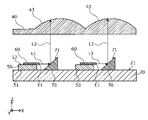
- the optical member 40 shown in FIGS. 1, 2, and 4 is a translucent plate member having a plurality of lens portions 43. As shown in FIG. The optical member 40 is supported by the frame member 30 and also functions as a lid for the area surrounded by the frame member 30 . Each of the plurality of lens portions 43 receives reflected light L2 from each reflecting surface 71 of each of the plurality of mirrors 70, as shown in FIG. In this embodiment, all of the multiple lens units 43 have the same focal length.
- the lens portion 43 is, for example, a spherical lens.
- the surface of the lens portion 43 facing the reflecting surface 71 is flat, and the surface on the back side (that is, outside) of the surface has a spherical convex shape.
- the lens portion 43 is a convex lens.
- the optical member 40 has the same number of lens portions 43 as the semiconductor laser chips 60 and the mirrors 70 .
- the plurality of lens units 43 are arranged in a matrix in the X-axis direction and the Y-axis direction, as shown in FIG.
- Each of the plurality of lens units 43 is arranged at a position corresponding to each of the plurality of mirrors 70 .
- 20 lens units 43 correspond to 20 mirrors 70 on a one-to-one basis.
- the optical member 40 is made of, for example, a translucent member such as glass.
- the optical member 40 has a lens region 44 in which a plurality of lens portions 43 are arranged, as shown in FIG.
- the lens region 44 is, for example, a region surrounded by an envelope 44E of the multiple lens portions 43 .
- a center position 44C of the lens area 44 is the center of gravity of the lens area 44 .
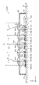
- FIG. 5 is a cross-sectional view illustrating optical paths in the light emitting device 10 according to this embodiment.
- FIG. 5 shows a partially enlarged view of a section similar to that of FIG. 2 and an optical path.
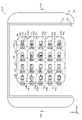
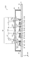
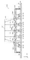
- FIG. 6 is a diagram showing the positional relationship between the multiple mirrors 70 and the multiple lens units 43 in the light emitting device 10 according to the present embodiment.
- FIG. 6 shows a plan view of the main surface 21 of the base 20 in plan view. In FIG. 6, the contours of the plurality of lens portions 43 are also shown by dashed lines.
- emitted light L1 emitted from the semiconductor laser chip 60 and having an optical axis parallel to the main surface 21 is reflected by the reflecting surface 71 of the mirror 70 and travels toward the lens portion 43 as reflected light L2.
- the direction of the optical axis of the reflected light L2 is parallel to the direction perpendicular to the main surface 21 of the base 20 .
- the reflected light L2 is incident on the lens portion 43 .
- the direction of the optical axis of the lens portion 43 is parallel to the direction perpendicular to the main surface 21 of the base 20 .
- the lens part 43 makes the reflected light L2, which is divergent light, in a parallel state or a converged state, and is output from the light emitting device 10 as the output light L3.
- the output light L3 from the lens portion 43 is directed in the optical axis direction of the lens portion 43. refract.
- the output light L3 is indicated by an arrow, this arrow indicates the optical axis of the output light L3, and the actual output light L3 has a width.
- the lens portion corresponding to the reflecting surface 71 among the plurality of lens portions 43 The following relationship holds for the distance in the X-axis direction to the center position 43C of 43 (hereinafter also referred to as first distance Dc).
- the distance Dc to the lens portion 43 located at the outermost side of the lens region 44 among the plurality of lens portions 43 is greater than the distance Dc to the lens portion 43 closest to the center position 44C of the lens region 44 among the plurality of lens portions 43. is large.
- the distance Dc increases as the distance (De) in the X-axis direction between the center position C1 of the emitted light L1 and the center position 44C of the lens region 44 where the plurality of lens portions 43 are arranged increases. so it gets bigger.
- the center position C1 of the emitted light L1 on the reflecting surface 71 is defined by the center position of the beam profile of the emitted light L1 or the position where the intensity of the emitted light L1 is maximized.
- a center position 43C of the lens portion 43 is defined at a position through which the optical axis of the lens portion 43 (one-dot chain line shown in FIG. 5) passes in plan view of the main surface 21 . Although no auxiliary line is shown in the drawing, the center position C1 of the emitted light L1 on the reflecting surface 71 also changes in the Y-axis direction as well.
- the X-axis direction from the center position 71C of the reflecting surface 71 to the center position 43C of the lens portion 43 corresponding to the reflecting surface 71 among the plurality of lens portions 43 in plan view of the main surface 21 The following relationship holds for the distance (hereinafter also referred to as the second distance).
- the second distance to the lens portion 43 that is located on the outermost side of the lens region 44 among the plurality of lens portions 43 is greater than the second distance to the lens portion 43 that is the closest to the center position 44C of the lens region 44 among the plurality of lens portions 43 .
- distance is greater.
- the second distance increases as the distance in the X-axis direction between the center position 71C of the reflecting surface 71 and the center position 44C of the lens area 44 increases.
- the center position C1 of the emitted light L1 on the reflecting surface 71 and the center position 71C of the reflecting surface 71 match. Note that the center position C1 of the emitted light L1 on the reflecting surface 71 and the center position 71C of the reflecting surface 71 do not have to match.
- the output light L3 from each of the plurality of lens portions 43 is irradiated inside the predetermined surface area A1 having an area smaller than that of the lens area 44.
- the predetermined surface area A1 having a smaller area than the lens area 44 is provided with no condensing lens between the optical member 40 and the predetermined surface area A1.
- a plurality of output lights L3 can be collected.
- the optical axes of all the output light beams L3 can be gathered in one place.
- the central position 71C of the reflecting surface 71 also changes in the Y-axis direction.
- the center position 43C of the lens portion 43 is on the line segment connecting the center position C1 of the emitted light L1 and the center position 44C of the lens region 44, but it is not necessarily strictly on the line segment. It doesn't have to be.
- the direction of the optical axis of each output light L3 is generally directed toward the center position of the lens region 44 in plan view, it does not necessarily have to be directed strictly toward the center position.
- the distance from the emission point E1 of the semiconductor laser chip 60 to the central position C1 of the emitted light L1 on the reflecting surface 71 is all the same.
- the effect of changes in the positions of the semiconductor laser chip 60 and the mirror 70 on the convergence state of the output light L3 can be greatly reduced.
- the center position C1 of the emitted light L1 on the reflecting surface 71 and the center position 71C of the reflecting surface 71 coincide with each other, the emitted light L1 can be efficiently reflected by the mirror 70 .
- the output light L3 is projected onto the predetermined surface region A1 having a smaller area than when the output light L3 is not a condensed beam. can be collected. In other words, the area of the far-field pattern formed by the multiple output lights L3 can be reduced. Therefore, it is possible to further increase the light density in the predetermined surface area A1.
- Light-emitting device 10 includes a plurality of semiconductor laser chips 60, as shown in FIG.
- Each of the plurality of semiconductor laser chips 60 is mounted on main surface 21 of base 20 and has an optical axis parallel to main surface 21 .
- a semiconductor laser chip 60 is mounted on the main surface 21 via a submount 50 .
- the submount 50 can be mounted without forming a fixing hole or the like in the base 20 , the submount 50 can be mounted on the base 20 without degrading the heat dissipation characteristics of the base 20 .
- the semiconductor laser chip 60 can be mounted on the base 20 only through the submount 50 .
- the semiconductor laser chip 60 can be mounted at a position close to the main surface 21 of the base 20 . Therefore, by using the submount 50 with high thermal conductivity, the heat radiation characteristic from the semiconductor laser chip 60 to the base 20 can be improved compared to the case where a CAN package including the semiconductor laser chip 60 is mounted on the base 20. can be done. As described above, according to the present embodiment, it is possible to realize the light emitting device 10 capable of improving the heat dissipation characteristics of the plurality of semiconductor laser chips 60 .
- the semiconductor laser chip 60 is mounted on each of the multiple submounts 50 .
- the semiconductor laser chip 60 is bonded to the mounting surface 52 of the submount 50 using a metallic bonding material.
- a Zener diode for maintaining a constant voltage supplied to the semiconductor laser chip 60 may also be joined to the mounting surface 52 of the submount 50 .
- the metallic bonding material for example, solder materials such as AuSn and AuGeNi, and bonding materials containing fine particles of Cu, Al, Au, Ag, and alloys thereof can be used.
- the submount 50 with the semiconductor laser chip 60 mounted thereon is mounted on the main surface 21 of the base 20 .
- the submount 50 is bonded to the main surface 21 of the base 20 using a metallic bonding material.
- the metallic bonding material for example, solder materials such as AuSn and AuGeNi, and bonding materials containing fine particles of Cu, Al, Au, Ag, and alloys thereof can be used.
- the submount 50 can be mounted on the base 20 .
- the frame member 30 is mounted on the base 20 in advance. Also, the frame member 30 may be formed integrally with the base 20 .
- a wire for supplying current to the semiconductor laser chip 60 is connected to the semiconductor laser chip 60 and the like.
- the terminals provided on the frame member 30 and the semiconductor laser chips 60 are connected by wires, and two adjacent semiconductor laser chips 60 are connected in series by wires.
- current can be supplied from the outside of the light emitting device 10 .
- the wire material is not particularly limited as long as it is conductive, and examples thereof include Au, Ag, and Cu.
- the mirror 70 is mounted on the main surface 21 of the base 20. Specifically, the mirror 70 is bonded to the main surface 21 of the base 20 using a metallic bonding material. Active alignment of the mirror 70 is performed before curing the metallic bonding material. In other words, a current is supplied to the semiconductor laser chip 60 to emit the emitted light L1, and while confirming the position of the emitted light L1 on the reflecting surface 71 of the mirror 70 and the position of the reflected light L2 from the mirror 70, The position of the mirror 70 on the main surface 21 is adjusted. After the alignment of the mirror 70 is completed, the metallic bonding material is cured in the same manner as when the submount 50 is mounted. Thereby, the mirror 70 can be mounted on the base 20 .
- the optical member 40 is mounted on the base 20.
- the optical member 40 is mounted on the base 20 via the frame member 30 .
- the optical member 40 is bonded to the frame member 30 using an adhesive or the like.
- the adhesive for example, a UV curable adhesive can be used.
- a UV curable adhesive is applied to at least one of the frame member 30 and the optical member 40 to temporarily fix the optical member 40 .
- active alignment of the positions of the optical member 40 in the X-, Y-, and Z-axis directions is performed.
- the UV curable adhesive is cured by irradiating it with UV light. Thereby, the optical member 40 can be mounted on the base 20 .
- the light emitting device 10 can be manufactured.
- a translucent member such as a cover glass may be attached between the optical member 40 and the frame member 30 .
- the plurality of lens portions 43 of the optical member 40 may be configured to be separable from the optical member 40 . In this case, the plurality of lens units 43 may be actively aligned individually.
- FIG. 7 and 8 are cross-sectional views of light-emitting devices according to modified examples 1 and 2 of the present embodiment, respectively.
- the plurality of lens portions 43 are arranged from the center position C1 of the emitted light L1 on the reflecting surface 71 in plan view of the main surface 21 .
- the distance (first distance) to the center position 43C of the lens portion 43 corresponding to the reflecting surface 71 is growing.
- the distance (second distance) from the center position 71C of the reflecting surface 71 to the center position 43C of the lens portion 43 corresponding to the reflecting surface 71 among the plurality of lens portions 43 in plan view of the main surface 21 is It increases as the distance from the center position 71C of the surface 71 to the center position 44C of the lens area 44 increases.
- the reflected light L2 incident on the left and right end lens portions 43 is emitted from the lens portion 43 as output light L3 having an optical axis inclined in a direction toward the center position 44C of the lens region 44 with respect to the optical axis of the reflected light L2. output. Therefore, according to the light emitting device 10A according to Modification 1 of the present embodiment, by appropriately selecting the irradiation distance from the lens region 44 to the predetermined surface region A1, the predetermined surface region A1 narrower than the lens region 44 has a plurality of light beams. Output light L3 can be emitted.
- the predetermined lens area having a smaller area than the lens area 44 is not arranged between the optical member 40 and the predetermined surface area A1.
- a plurality of output lights L3 can be condensed on the surface area A1.
- the distance and the second distance are zero.
- the first distance and the second distance are values other than zero in the left end and right end lens portions 43 among the plurality of lens portions 43 .
- the optical axis of the reflected light L2 is located outside the lens area 44 (farther from the center position 44C) than the center position 43C of the lens portion 43.
- the first distance and the second distance are is about 1/10 of the first distance and the second distance with respect to the lens portion 43 of .
- the optical axis of the reflected light L2 corresponding to the lens portion 43 is located inside the lens area 44 ( position close to the center position 44C).
- the first distance and the second distance are is about 1/10 of the first distance and the second distance with respect to the lens portion 43 of .
- the optical axis of the reflected light L2 corresponding to the lens portion 43 is positioned closer to the lens region 44 than the center position 43C of the lens portion 43 located between the center lens portion 43 and the right end lens portion 43. It is located inside (a position close to the center position 44C).
- the reflected light L2 incident on the lens portion 43 closest (center) to the center position 44C of the lens region 44 is parallel to the reflected light L2 without substantially being refracted. It is output from the lens portion 43 as propagating output light L3.
- the reflected light L2 incident on the two lens portions 43 between the center and the left and right ends is output from the lens portion 43 as output light L3 having an optical axis slightly inclined away from the center position 44C of the lens area 44. be.
- the reflected light L2 incident on the lens portions 43 at the left and right ends is output from the lens portion 43 as output light L3 having an optical axis inclined toward the center position 44C of the lens region 44 with respect to the optical axis of the reflected light L2.
- the relationship between the center position 71C of the reflecting surface 71 of the mirror 70 and the center position 43C of the lens portion 43 of the light emitting device according to the present embodiment is not limited to the relationship in the light emitting device 10 described above. That is, the first distance to the lens portion 43 that is closest to the center position 44C of the lens region 44 among the plurality of lens portions 43 is greater than the first distance to the lens portion 43 that is positioned on the outermost side of the lens region 44 among the plurality of lens portions 43 . The first distance should be larger.
- the second distance to the lens portion 43 that is closest to the center position 44C of the lens region 44 among the plurality of lens portions 43 is longer than the second distance to the lens portion 43 that is positioned on the outermost side of the lens region 44 among the plurality of lens portions 43 .
- the second distance should be larger.
- the first distance to all the lens portions 43 located on the outermost side of the lens region 44 may not be larger than the first distance to the lens portion 43 closest to the center position 44C of the lens region 44. , the first distance from at least one of the lens portions 43 located on the outermost side of the lens area 44 should be larger.
- the second distance to all of the lens portions 43 located on the outermost side of the lens region 44 may not be greater than the second distance to the lens portion 43 closest to the center position 44C of the lens region 44. , the second distance from at least one of the lens portions 43 located on the outermost side of the lens area 44 should be larger.
- Embodiment 2 A light-emitting device according to Embodiment 2 will be described.
- the positions of the mirror 70 and the semiconductor laser chip 60 with respect to the lens portion 43 are adjusted according to the distance from the center position 44C of the lens region 44 to the center position 71C of the reflecting surface 71 of the mirror 70. While maintaining the relationship, the position in the plane view was changed.
- the light emitting device according to the present embodiment does not change the positions of the mirror 70 and the semiconductor laser chip 60 with respect to the lens portion 43, but changes the height of the optical axis of the emitted light L1 from the main surface 21 of the base 20.
- Embodiment 1 It is different from the light-emitting device 10 according to Embodiment 1 in that The light-emitting device according to the present embodiment will be described below with reference to FIGS. 9 and 10, focusing on differences from the light-emitting device 10 according to the first embodiment.
- FIG. 9 is a plan view showing a state in which the optical member 40 is removed from the light emitting device 110 according to this embodiment.
- FIG. 9 shows a plan view of the main surface 21 of the base 20 in plan view.
- the contours of the plurality of lens portions 43 are also shown by dashed lines.
- FIG. 10 is a cross-sectional view of light emitting device 110 according to this embodiment.
- FIG. 10 shows a cross section along line XX in the X-axis direction of FIG. Note that FIG. 10 also shows a cross section of the optical member 40 .
- the light emitting device 110 includes a base 20, a frame member 30, an optical member 40, a plurality of semiconductor laser chips 60, a plurality of submounts 53a to 53d, 54a to 54d, 55a to 55d, 56a-56d, 57a-57d and a plurality of mirrors 70 are provided.
- the relative positions of each of the plurality of mirrors 70 and each of the plurality of lens portions 43 in plan view of the main surface 21 of the base 20 are all the same. Same for mirror 70 .
- the center position 43C of each of the plurality of lens portions 43 and the center position of the reflecting surface 71 corresponding to each of the plurality of lens portions 43 71C matches.
- the distances from the emission point E1 of the semiconductor laser chip 60 to the center position 71C of the reflecting surface 71 are all the same. In other words, the positional relationship between the semiconductor laser chip 60 and the mirror 70 is the same.
- the plurality of submounts 53a to 53d, 54a to 54d, 55a to 55d, 56a to 56d, and 57a to 57d differ from the submount 50 according to Embodiment 1 in that they are different in height. different.
- the direction of the optical axis of the reflected light L2 is parallel to the direction perpendicular to the main surface 21 because the angle of the reflecting surface with respect to the main surface is 45°.
- the difference between the height from the main surface 21 to the emission point E1 of each of the plurality of semiconductor laser chips 60 and the average value Ha1 of the heights from the main surface 21 to the emission point E1 of each of the plurality of semiconductor laser chips 60 The following relationship holds for the absolute value (hereinafter also referred to as the first difference D1). Outermost of the lens area 44 among the plurality of lens sections 43 than the first difference D1 with respect to the emission point E1 corresponding to the lens section 43 closest to the center position 44C of the lens area 44 among the plurality of lens sections 43 The first difference D1 with respect to the emission point E1 corresponding to the lens portion 43 corresponding to the corresponding lens portion 43 is larger.
- the first difference D1 increases as the distance from the center position 44C of the lens region 44 to the center position 43C of the lens portion 43 corresponding to each of the plurality of submounts among the plurality of lens portions 43 increases. Become. Therefore, the distance of the optical axis of the semiconductor laser chip 60 from the main surface 21, that is, the position of the emitted light L1 on the reflecting surface 71 in the X-axis direction varies depending on the height of the submount.
- a plurality of The distance in the X-axis direction from the center position C1 of the emitted light L1 to the center position 43C of the lens part 43 corresponding to the reflecting surface 71 is the lens area 44 where the plurality of lens parts 43 are arranged. increases as the distance in the X-axis direction to the center position 44C of the increases. Therefore, the position of the reflected light L2 incident on each of the plurality of lens portions 43 according to the present embodiment is the same as in the first embodiment in the X-axis direction, and the output light L3 is reflected in the lens area 44 in the X-axis direction.
- each output light L3 is generally directed to the central position of the lens region 44 in the X-axis direction in a plan view, but it is not necessarily strictly directed. It doesn't have to be.
- the plurality of output lights L3 can be condensed on the predetermined surface area A1 having an area smaller than that of the lens area 44 without arranging a condensing lens.
- a plurality of output light beams L3 can be condensed on a predetermined surface region A1 having an area smaller than that of the lens region 44 without arranging a condensing lens.
- the main surface 21 of the base 20 parallel to the emitted light L1 and the reflecting surface 71 is 45°, even if the height from the main surface 21 to the position of the emission point E1 of the semiconductor laser chip 60 changes, the emission from the emission point E1 of the semiconductor laser chip 60 on the reflecting surface 71
- the sum of the distance to the center position of the emitted light L1 and the distance from the center position of the emitted light L1 on the reflecting surface 71 to the lens portion 43 is constant, and the height from the main surface 21 to the position of the emission point E1 of the semiconductor laser chip 60 is constant. It is possible to greatly reduce the influence of the light intensity on the convergence state of the output light L3.
- each of the plurality of semiconductor laser chips 60 is mounted on main surface 21 and , the same effect of improving heat dissipation characteristics as the light emitting device 10 according to the first embodiment can be obtained.
- FIG. 11 is a cross-sectional view of a light emitting device 110A according to this modification.
- the difference (first difference D1) between the average value Ha1 of the heights up to the emission point E1 of each of the plurality of semiconductor laser chips 60 is the emission point of the plurality of lens portions 43 from the center position 44C of the lens region 44. It increases as the distance to the center position 43C of the lens portion 43 corresponding to E1 increases.
- the light-emitting device 110A as shown in FIG. has a first difference D1 of zero.
- the first difference is not zero in the lens portions 43 located on the outermost side of the lens area 44 among the plurality of lens portions 43 (the leftmost and rightmost lens portions 43 in FIG. 11).
- the reflected light L2 incident on the left and right end lens portions 43 is emitted from the lens portion 43 as output light L3 having an optical axis inclined in a direction toward the center position 44C of the lens region 44 with respect to the optical axis of the reflected light L2. output. Therefore, according to the light emitting device 110A according to this modified example, by appropriately selecting the irradiation distance from the lens region 44 to the predetermined surface region A1, the predetermined surface region A1 narrower than the lens region 44 is irradiated with the plurality of output light beams L3. can do.
- a plurality of condenser lenses are not disposed between the optical member 40 and the predetermined surface area A1, and the predetermined surface area A1 having an area smaller than that of the lens area 44 has a plurality of lenses.
- output light L3 can be condensed.
- the relationship between the center position of the emitted light L1 of the light emitting device according to the present embodiment and the center position 43C of the lens portion 43 is not limited to the relationship in the light emitting device 110 described above. That is, the outermost position of the lens region 44 among the plurality of lens portions 43 is greater than the first difference D1 with respect to the emission point E1 corresponding to the lens portion 43 closest to the center position 44C of the lens region 44 among the plurality of lens portions 43 . It is sufficient if the first difference D1 with respect to the emission point E1 corresponding to the lens portion 43 located at is larger.
- the first difference for all the emission points E1 corresponding to the lens portions 43 located on the outermost side of the lens region 44 is greater than the first difference for the emission points E1 corresponding to the lens portions 43 closest to the center position 44C of the lens region 44.
- the first difference D1 does not have to be large, and the first difference D1 with respect to at least one emission point E1 corresponding to the lens portion 43 located on the outermost side of the lens area 44 may be larger.
- Embodiment 3 A light-emitting device according to Embodiment 3 will be described.
- the height of the optical axis of the emitted light L1 from the main surface 21 is the same for all the semiconductor laser chips 60, and the height of the reflecting surface 71 from the main surface 21 is changed. It differs from the light emitting device 110 according to Embodiment 2 in that the distance between the emission point E1 and the center position 71C of the reflecting surface 71 is changed in plan view.
- the light emitting device according to the present embodiment will be described below with reference to FIGS. 12 and 13, focusing on differences from the light emitting device 110 according to the second embodiment.
- FIG. 12 is a plan view showing a state in which the optical member 40 is removed from the light emitting device 210 according to this embodiment.
- FIG. 12 shows a plan view of the main surface 21 of the base 20 in plan view.
- the contours of the plurality of lens portions 43 are shown together with dashed lines.
- FIG. 13 is a cross-sectional view of light emitting device 210 according to this embodiment.
- FIG. 13 shows a cross section along line XIII-XIII of FIG. Note that FIG. 13 also shows a cross section of the optical member 40 .
- a light emitting device 210 includes a base 20, a frame member 30, an optical member 40, a plurality of semiconductor laser chips 60, a plurality of submounts 50, a plurality of mirrors 73a-73d, 74a- 74d, 75a-75d, 76a-76d, 77a-77d.
- the multiple submounts 50 according to the present embodiment have the same configuration as the multiple submounts 50 according to the first embodiment. Therefore, the distances of the optical axes of the semiconductor laser chips 60 mounted on the plurality of submounts 50 from the main surface 21 are all the same.
- Each of the plurality of mirrors 73a to 73d, 74a to 74d, 75a to 75d, 76a to 76d, and 77a to 77d has a reflecting surface 71 like the mirror 70 according to the second embodiment.
- the relative positions of each of the plurality of mirrors and each of the plurality of lens portions 43 are the same for all mirrors.
- the center position 43C of each of the plurality of lens portions 43 and the center position of the reflecting surface 71 corresponding to each of the plurality of lens portions 43 71C matches.
- the heights of the central position 71C of the reflecting surface 71 from the main surface 21 are not the same. different from The direction of the optical axis of the reflected light L2 is parallel to the direction perpendicular to the main surface 21 because the angle of the reflecting surface 71 with respect to the main surface 21 is 45°.
- the absolute value of the difference between the height from the main surface 21 to the center position 71C of the reflecting surface 71 and the average value Ha2 of the heights from the main surface 21 to the center position 71C of the reflecting surface 71 at a plurality of mirrors (hereinafter referred to as second difference D2), the following relationship holds: Out of the plurality of lens portions 43, the outermost portion of the lens region 44 is positioned more than the second difference D2 with respect to the reflecting surface 71 corresponding to the lens portion 43 closest to the center position 44C of the lens region 44 among the plurality of lens portions 43.
- the second difference D2 with respect to the reflecting surface 71 corresponding to the lens portion 43 corresponding to the second difference D2 is larger.
- the second difference D2 increases as the distance from the center position 44C of the lens region 44 to the center position 43C of the lens portion 43 corresponding to each of the plurality of mirrors among the plurality of lens portions 43 increases. . Therefore, the position of the emitted light L1 on the reflecting surface 71 in the X-axis direction differs depending on the height of the central position 71C of the reflecting surface 71 from the main surface 21 .
- a plurality of The distance from the center position C1 of the emitted light L1 to the center position 43C of the lens area 44 where the plurality of lens parts 43 are arranged is increases as the distance to Therefore, the position of the reflected light L2 incident on each of the plurality of lens portions 43 according to the present embodiment is the same as in the first embodiment in the X-axis direction, and the output light L3 is reflected in the lens area 44 in the X-axis direction. refracts toward the center of On the other hand, there is no bending in the Y-axis direction.
- the direction of the optical axis of each output light L3 is roughly directed to the central position of the lens region 44 in the X-axis direction in a plan view, but it is not necessarily strictly directed. It doesn't have to be. Therefore, in the light-emitting device 210 according to the present embodiment as well, the plurality of output lights L3 can be condensed onto the predetermined surface area A1 having an area smaller than that of the lens area 44 without arranging a condensing lens.
- the absolute value of the difference from the average height of the reflecting surface 71 to the center position 71C is proportional to De, so that the optical axis of all the output light beams L3 is approximately 1 or 1. can be collected in place.
- the angle formed by the emitted light L1 and the reflecting surface 71 is 45°, the emitted light L1 on the reflecting surface 71 is equal to the amount of change in height from the main surface 21 to the center position 71C of the reflecting surface 71.
- the distance from the center position of the to the lens portion 43 is shortened. Therefore, as shown in FIG.
- FIG. 14 is a cross-sectional view of a light emitting device 210A according to this modification.
- the second difference D2 is zero.
- the second difference D2 is not zero in the lens portions 43 (the leftmost and rightmost lens portions 43 in FIG. 14) located on the outermost side of the lens area 44 among the plurality of lens portions 43 .
- the reflected light L2 incident on the three central lens portions 43 is output from the lens portions 43 as three output light beams L3 whose optical axes are parallel to each other.
- the reflected light L2 incident on the left and right end lens portions 43 is emitted from the lens portion 43 as output light L3 having an optical axis inclined in a direction toward the center position 44C of the lens region 44 with respect to the optical axis of the reflected light L2. output. Therefore, according to the light emitting device 210A according to this modified example, by appropriately selecting the irradiation distance from the lens area 44 to the predetermined surface area A1, the predetermined surface area A1 narrower than the lens area 44 is irradiated with the plurality of output light beams L3. can do.
- a plurality of condenser lenses are not disposed between the optical member 40 and the predetermined surface area A1, and the predetermined surface area A1 having an area smaller than that of the lens area 44 has a plurality of lenses.
- output light L3 can be condensed.
- the relationship between the position of the optical axis of the reflected light L2 of the light emitting device according to the present embodiment and the center position 43C of the lens portion 43 is not limited to the relationship in the light emitting device 210 described above. That is, the second difference D2 with respect to the reflecting surface 71 corresponding to the lens portion 43 closest to the center position 44C of the lens region 44 among the plurality of lens portions 43 is greater than the outermost portion of the lens region 44 among the plurality of lens portions 43 . It is sufficient if the second difference D2 with respect to the reflecting surface 71 corresponding to the lens portion 43 located at is larger.
- All of the reflecting surfaces 71 corresponding to the lens portion 43 located on the outermost side of the lens region 44 are larger than the second difference D2 with respect to the reflecting surface 71 corresponding to the lens portion 43 closest to the center position 44C of the lens region 44. It is not necessary that the second difference D2 with respect to .theta.
- Embodiment 4 A light-emitting device according to Embodiment 4 will be described.
- the light emitting device according to the present embodiment differs from the light emitting device 10 according to Embodiment 1 mainly in that the direction of the optical axis of at least part of the reflected light L2 is different from the direction of the optical axis of the lens portion 43. differ.
- the light emitting device according to the present embodiment will be described below with reference to FIGS. 15 and 16, focusing on differences from the light emitting device 10 according to the first embodiment.
- FIG. 15 is a plan view showing a state in which the optical member 40 is removed from the light emitting device 310 according to this embodiment.
- FIG. 15 shows a plan view of the main surface 21 of the base 20 in plan view.
- the contours of the plurality of lens portions 43 are shown together with dashed lines.
- FIG. 16 is a cross-sectional view of light emitting device 310 according to this embodiment.
- FIG. 16 shows a cross section along line XVI--XVI of FIG. Note that FIG. 16 also shows a cross section of the optical member 40 .
- a light emitting device 310 includes a base 20, a frame member 30, an optical member 40, a plurality of semiconductor laser chips 60, a plurality of submounts 50, a plurality of mirrors 373a to 373d, 374a to 374d, 375a-375d, 376a-376d, 377a-377d.
- the direction perpendicular to the reflecting surface 71 of each mirror is projected onto the main surface 21 (for example, the direction of the dashed arrow 71D shown in the mirror 374b in FIG. 15).
- each mirror is arranged so as to be in a direction parallel to a two-dot chain line connecting
- the direction of the optical axis of the emitted light L1 from each semiconductor laser chip 60 is such that the direction perpendicular to the reflection surface 71 on which the emitted light L1 is incident coincides with the direction projected onto the main surface 21. and a submount 50 are arranged.
- Each of the plurality of mirrors according to the present embodiment has a reflecting surface 71 like the mirror 70 according to the first embodiment.
- the plurality of mirrors according to the present embodiment are the same as those in the first embodiment in that the optical axis of the reflected light L2 passes through the optical center of the lens portion 43.
- the tilt differs from the mirror 70 according to the first embodiment.
- the angle formed by the direction Dm perpendicular to the main surface 21 and the direction D71 perpendicular to the reflecting surface 71 see the angle ⁇ r at the mirror 375a in FIG. 16
- the average of the angles formed by the plurality of mirrors The following relationship holds for the absolute value of the difference from the value (hereinafter also referred to as the third difference).
- the third difference with respect to the reflecting surface 71 corresponding to the lens portion 43 is larger.
- the third difference increases as the distance from the center position 44C of the lens region 44 to the center position 43C of the lens portion 43 corresponding to the reflecting surface 71 among the plurality of lens portions 43 increases.
- the angle formed by the direction of the optical axis of the reflected light L2 and the direction perpendicular to the main surface 21 (or the direction of the optical axis of the lens portion 43) (hereinafter also referred to as the first angle (see angle ⁇ 1 in FIG. 16) ))))
- the first angle (see angle ⁇ 1 in FIG. 16) ))
- the following relationship holds: Positioned on the outermost side of the lens region 44 among the plurality of lens portions 43 than the first angle ⁇ 1 with respect to the reflected light L2 corresponding to the lens portion 43 closest to the center position 44C of the lens region 44 among the plurality of lens portions 43
- the first angle ⁇ 1 with respect to the reflected light L2 corresponding to the lens portion 43 is larger.
- the first angle ⁇ 1 increases as the distance from the center position 44C of the lens region 44 to the center position 43C of the lens portion 43 that receives the reflected light L2 among the plurality of lens portions 43 increases.
- the optical axis of the reflected light L2 passes through the center position (optical center) of the lens portion 43, so that the optical axis of the lens portion 43 and the optical axis of the reflected light L2
- the reflected light L2 and the output light L3 propagate in the same direction even if there is a deviation.
- the optical axis of the output light L3 is tilted with respect to the optical axis of the lens portion 43 without refracting the optical axis of the reflected light L2 by the lens portion 43, and the output light L3 is focused on the predetermined surface area A1.
- the optical axis of the reflected light L2 does not need to be refracted by the lens portion 43, so that the reflected light L2 can enter the vicinity of the optical axis of the lens portion 43. Therefore, since the coma aberration of the output light L3 can be reduced, distortion of the profile of the output light L3 in the predetermined surface area A1 can be suppressed. That is, the output light L3 can be reliably focused on the predetermined surface area A1.
- the absolute value of the difference from the average value of the formed angles is proportional to the distance from the center position 44C of the lens region 44 to the center position 43C of the lens portion 43, so that the optical axis of all the output light L3 is It can be collected in almost one place.
- the directions of the optical axes of the reflected light beams L2 and the output light beams L3 are generally directed toward the central position of the lens area 44 in a plan view, but they are not necessarily strictly aligned. It does not have to be facing the center position.
- the angle formed by the direction perpendicular to the reflecting surface 71 projected onto the main surface 21 and the incident direction of the emitted light L1 onto the reflecting surface 71 is the same angle.
- the angle is 0°.
- the sum of the distance from the emission point E1 of the semiconductor laser chip 60 to the central position of the emitted light L1 on the reflecting surface 71 and the distance from the central position of the emitted light L1 on the reflecting surface 71 to the lens portion 43 is constant.
- FIG. 17 is a cross-sectional view of a light emitting device 310A according to this modification.
- the absolute value (third difference) of the difference from the average value of the angles formed by the mirror is obtained from the center position 44C of the lens region 44 to the center of the lens portion 43 corresponding to the reflecting surface 71 among the plurality of lens portions 43. It increases as the distance to position 43C increases. Further, the angle (first angle ⁇ 1) formed by the direction of the optical axis of the reflected light L2 and the direction perpendicular to the main surface 21 is determined from the center position 44C of the lens region 44 by the reflected light L2 among the plurality of lens portions 43. increases as the distance to the center position 43C of the lens portion 43 that receives the distance increases.
- the light-emitting device 310A as shown in FIG. is zero for the third difference and the first angle. Further, the third difference and the first angle are not zero in the lens portions 43 (the leftmost and rightmost lens portions 43 in FIG. 17) located on the outermost side of the lens area 44 among the plurality of lens portions 43 .
- the reflected light L2 incident on the three central lens portions 43 is output from the lens portions 43 as three output light beams L3 whose optical axes are parallel to each other.
- the reflected light L2 incident on the left and right end lens portions 43 is output from the lens portion 43 as output light L3 having an optical axis inclined toward the center position 44C of the lens area 44 .
- the predetermined surface region A1 narrower than the lens region 44 is irradiated with the plurality of output light beams L3. can do.
- a plurality of condenser lenses are not disposed between the optical member 40 and the predetermined surface area A1, and the predetermined surface area A1 having an area smaller than the lens area 44 has a plurality of lenses.
- output light L3 can be condensed.
- the relationship between the distance from the center position 44C of the lens region 44 of the lens portion 43 of the light emitting device according to the present embodiment and the inclination of the reflecting surface 71 corresponding to the lens portion 43 is the same as that of the light emitting device 310 described above. is not limited to the relationship in That is, the outermost portion of the lens region 44 among the plurality of lens portions 43 is closer to the reflecting surface 71 than the third difference with respect to the reflecting surface 71 corresponding to the lens portion 43 closest to the center position 44C of the lens region 44 among the plurality of lens portions 43 .
- the third difference with respect to the reflecting surface 71 corresponding to the lens portion 43 located should be larger.
- the outermost angle of the lens region 44 among the plurality of lens portions 43 is greater than the first angle ⁇ 1 with respect to the reflected light L2 corresponding to the lens portion 43 closest to the center position 44C of the lens region 44 among the plurality of lens portions 43 . It is sufficient if the first angle ⁇ 1 with respect to the reflected light L2 corresponding to the lens portion 43 located at is larger.
- the reflecting surfaces 71 corresponding to the lens portion 43 located on the outermost side of the lens region 44 than the third difference to the reflecting surface 71 corresponding to the lens portion 43 closest to the center position 44C of the lens region 44.
- the third difference does not have to be large, and the third difference with respect to at least one of the reflecting surfaces 71 corresponding to the lens portion 43 located on the outermost side of the lens area 44 may be larger.
- Embodiment 5 A light-emitting device according to Embodiment 5 will be described.
- the light-emitting device according to this embodiment differs from the light-emitting device 310 according to the fourth embodiment in the configuration of the plurality of mirrors.
- the light emitting device according to the present embodiment will be described below with reference to FIGS. 18 and 19, focusing on differences from the light emitting device 310 according to the fourth embodiment.
- FIG. 18 is a plan view showing a state in which the optical member 40 of the light emitting device 410 according to this embodiment is removed.
- FIG. 18 shows a plan view of the main surface 21 of the base 20 in plan view.
- the contours of the plurality of lens portions 43 are also shown by dashed lines.
- FIG. 19 is a cross-sectional view of light emitting device 410 according to this embodiment.
- FIG. 19 shows a cross section along line XIX-XIX in FIG. Note that FIG. 19 also shows a cross section of the optical member 40 .
- a light emitting device 410 includes a base 20 , a frame member 30 , an optical member 40 , multiple semiconductor laser chips 60 , multiple submounts 50 , and multiple mirrors 470 .
- light emitting device 410 further includes a plurality of support portions 83a-83d, 84a-84d, 85a-85d, 86a-86d, 87a-87d, as shown in FIG.
- the support portion may be formed integrally with the base, or may be formed of separate members.
- Each of the plurality of mirrors 470 is a plate-like element having a reflecting surface 71, as shown in FIG.
- each of the plurality of mirrors 470 has a plate-like shape with the rectangular reflecting surface 71 as one main surface.
- each of the plurality of mirrors 470 has a cuboid shape.
- the plurality of mirrors 470 are respectively leaned against the plurality of supports 83a-83d, 84a-84d, 85a-85d, 86a-86d, 87a-87d.
- each of the plurality of mirrors 470 may be joined to the main surface 21 of the base 20 and the corresponding support portion with a joining material or the like.
- the plurality of supporting portions form steps with main surface 21 .
- the multiple supports have different dimensions. Specifically, as shown in FIG. 19, the height of the supporting portion from the main surface 21 (see the height Hs of the supporting portion 85d shown in FIG. 19) and The absolute value (
- the positional relationship among the emitted light L1 from the semiconductor laser chip 60, the reflected light L2 from the reflecting surface 71, and the output light L3 from the lens portion 43 is the same as in the fourth embodiment. , the same effect as in the fourth embodiment can be obtained.
- the absolute value of the difference from the average value of the formed angles is proportional to the distance from the center position 44C of the lens area 44 to the center position 43C of the lens portion 43, so that the optical axis of all the output light L3 is approximately can be collected in one place.
- the tilt angle of each of the plurality of mirrors 470 with respect to the main surface 21 of the base 20 can be adjusted, fine optical axis adjustment is possible.
- the structure of the plurality of mirrors 470 can be made common, the manufacturing of the plurality of mirrors 470 can be facilitated, and the cost required for the plurality of mirrors 470 can be reduced.
- Embodiment 6 A light-emitting device according to Embodiment 6 will be described.
- the light-emitting device according to the present embodiment differs from the light-emitting device 310 according to the fourth embodiment mainly in the configuration of the multiple semiconductor laser chips 60 and the multiple mirrors 70 .
- the light-emitting device according to the present embodiment will be described below with reference to FIG. 20, focusing on differences from the light-emitting device 310 according to the fourth embodiment.
- FIG. 20 is a plan view showing a state in which the optical member 40 is removed from the light emitting device 510 according to this embodiment.
- FIG. 20 shows a plan view of the main surface 21 of the base 20 in plan view.
- the contours of the plurality of lens portions 43 are shown together with dashed lines, and the optical axis of the reflected light L2 from the mirror 70 and the optical axis of the output light L3 are also shown together.
- a light emitting device 510 includes a base 20, a frame member 30, an optical member 40, a plurality of semiconductor laser chips 60, a plurality of submounts 50, and a plurality of mirrors .
- the plurality of semiconductor laser chips 60, the plurality of submounts 50, and the plurality of mirrors 70 are the plurality of semiconductor laser chips 60, the plurality of submounts 50, and the plurality of mirrors 70 according to Embodiment 1, respectively, except for the arrangement. , has a configuration similar to that of the plurality of mirrors 70 .
- the angle of the reflecting surface 71 of the mirror 70 with respect to the main surface 21 of the base 20 is 45°.
- the direction A the direction of the dashed line in FIG. 20, that is, the X-axis direction
- the reflected light L2 is projected onto the base 20. It proceeds in a direction B (the Z-axis direction) perpendicular to the main surface 21 (in the drawing, this direction is indicated by a small black circle in the center of a white circle).
- the vector of the emitted light L1 is decomposed into a direction A and a direction C (Y direction) orthogonal to the direction A in a plane parallel to the main surface 21, then the vector of the reflected light L2 is divided into the direction B and It will have a component with direction C. That is, in a plan view, the reflected light L2 faces the direction C (Y-axis direction).
- the direction perpendicular to the reflecting surface 71 of the mirror 70 is projected onto the main surface 21 of the base 20, and the emitted light from the semiconductor laser chip 60
- the direction of the reflected light L2 is tilted with respect to the direction perpendicular to the main surface 21 by adjusting the angle formed by the direction of the optical axis of L1.
- the direction perpendicular to the reflecting surface 71 is projected onto the main surface 21 (the dashed line direction shown in FIG. 20) and the direction of the emitted light L1 (the dashed line direction shown in FIG. 20).
- the second angle .theta.2 with respect to the reflecting surface 71 corresponding to the lens portion 43 is larger. Also, the second angle ⁇ 2 increases as the distance from the center position 44C of the lens region 44 to the center position 43C of the lens portion 43 corresponding to the reflecting surface 71 among the plurality of lens portions 43 increases.
- the angle formed by the direction of the optical axis of the reflected light L2 and the direction perpendicular to the main surface 21 is shifted from the center position 44C of the lens region 44 to the position of the lens portion 43 that receives the reflected light L2 among the plurality of lens portions 43. It increases as the distance to the center position increases. Therefore, in the light-emitting device 510 according to the present embodiment as well as in the light-emitting device 310 according to the fourth embodiment, the angle formed by the direction of the optical axis of the reflected light L2 and the direction perpendicular to the main surface 21 is the lens region 44.
- the same light condensing effect is achieved.
- the output light L3 when the optical axis of the reflected light L2 passes through a position deviated from the center position 43C of the lens section, the output light L3 changes its direction toward the center position of the lens section. 20, the output light L3 can be directed toward the central position 44C of the lens area 44 (see the arrow indicating the output light L3 in FIG. 20). In other words, a plurality of output lights L3 can be condensed on the predetermined surface area A1.
- this angle is approximately proportional to the distance from the center position 44C of the lens region 44 to the center position 43C of the lens portion 43, the optical axes of all the output light L3 can be converged at approximately one point. .
- the configuration of the light emitting device 510 can be simplified.
- the direction perpendicular to the reflecting surface 71 of the mirror 70 is projected onto the main surface, which is the direction of the dashed line shown for each mirror 70 in FIG. (that is, the X-axis direction in FIG. 20). Since the orientations of the plurality of mirrors 70 can be unified in this manner, the plurality of mirrors 70 can be aligned. Therefore, mounting of the plurality of mirrors 70 can be facilitated.
- the angle of the direction perpendicular to the reflecting surface 71 with respect to the main surface 21 is the same angle (45°) for all the plurality of mirrors 70 . Since the same mirror can be used as the plurality of mirrors 70 in this manner, the configuration of the light emitting device 510 can be simplified. In addition, since the reflecting surfaces 71 of a plurality of mirrors arranged in a row can be set on the same plane, the plurality of mirrors can be replaced with one mirror connected in the row direction, further simplifying the configuration.
- FIG. 21 is a cross-sectional view of a light emitting device 510A according to this modification.
- the angle (second angle ⁇ 2) increases as the distance from the center position 44C of the lens region 44 to the center position 43C of the lens portion 43 corresponding to the reflecting surface 71 among the plurality of lens portions 43 increases.
- the center position 44C of the lens region 44 is closer to the center position 44C (other than the outermost lens portion 43).
- the second angle .theta.2 is zero in the nine lens portions of .
- the second angle ⁇ 2 is not zero but 20 degrees.
- the second angle ⁇ 2 with respect to the reflecting surface 71 corresponding to the lens portions 43 other than the four corner lens portions 43 among the outermost lens portions 43 of the lens region 44 is zero, and the reflected light L2 is The incident position on the lens portion 43 is shifted from the center position 43C of the lens portion 43 toward the outside of the lens area 44 .
- the reflected light L2 incident on these lens portions 43 is output from the lens portions 43 as output light L3 having an optical axis inclined toward the center position 44C of the lens region 44 .
- the predetermined surface region A1 narrower than the lens region 44 is irradiated with the plurality of output light beams L3. can do.
- a plurality of condenser lenses are not disposed between the optical member 40 and the predetermined surface region A1, and the predetermined surface region A1 having an area smaller than the lens region 44 has a plurality of lenses.
- output light L3 can be condensed.
- the aspect of the angle formed by the direction of projection of the direction perpendicular to the reflecting surface 71 of the lens portion 43 of the light emitting device according to the present embodiment onto the main surface 21 and the direction of the emitted light L1 It is not limited to the aspects in device 510 . That is, the second angle ⁇ 2 with respect to the reflecting surface 71 corresponding to the lens portion 43 closest to the center position 44C of the lens region 44 among the plurality of lens portions 43 is larger than the outermost angle of the lens region 44 among the plurality of lens portions 43 . It is sufficient if the second angle ⁇ 2 with respect to at least one of the reflecting surfaces 71 corresponding to the lens portion 43 located at is larger.
- Embodiment 7 A light-emitting device according to Embodiment 7 will be described.
- the light-emitting device according to the present embodiment differs from the light-emitting device 510 according to the sixth embodiment mainly in the configuration of the plurality of semiconductor laser chips 60 and the plurality of mirrors 70 .
- the light-emitting device according to the present embodiment will be described below with reference to FIG. 22, focusing on differences from the light-emitting device 510 according to the sixth embodiment.
- FIG. 22 is a plan view showing a state in which the optical member 40 of the light emitting device 610 according to this embodiment is removed.
- FIG. 22 shows a plan view of the main surface 21 of the base 20 in plan view.
- the contours of the plurality of lens portions 43 are shown together with dashed lines, and the optical axis of the reflected light L2 from the mirror 70 and the optical axis of the output light L3 are also shown together.
- a light emitting device 610 includes a base 20, a frame member 30, an optical member 40, a plurality of semiconductor laser chips 60, a plurality of submounts 50, and a plurality of mirrors .
- the plurality of semiconductor laser chips 60, the plurality of submounts 50, and the plurality of mirrors 70 are the plurality of semiconductor laser chips 60, the plurality of submounts 50, and the plurality of mirrors 70 according to Embodiment 1, respectively, except for the arrangement. , has a configuration similar to that of the plurality of mirrors 70 .
- the direction perpendicular to the reflecting surface 71 of the mirror 70 is projected onto the main surface 21 of the base 20 (Fig. 22) and the direction of the optical axis of the emitted light L1 from the semiconductor laser chip 60 (the direction of the dashed line shown in FIG. 22). are inclined with respect to the direction perpendicular to the main surface 21 .
- the direction perpendicular to the reflecting surface 71 of the mirrors 70 is changed according to the distance from the center position 44C of the lens region 44.
- FIG. Specifically, the direction perpendicular to the reflecting surface 71 is projected onto the main surface 21 (the direction of the dashed line shown in FIG.
- the second angle ⁇ 2 Positioned on the outermost side of the lens area 44 among the plurality of lens sections 43 relative to the second angle ⁇ 2 with respect to the reflecting surface 71 corresponding to the lens section 43 closest to the center position 44C of the lens area 44 among the plurality of lens sections 43
- the second angle .theta.2 with respect to the reflecting surface 71 corresponding to the lens portion 43 is larger.
- the second angle ⁇ 2 increases as the distance from the center position 44C of the lens region 44 to the center position 43C of the lens portion 43 corresponding to the reflecting surface 71 among the plurality of lens portions 43 increases.
- the optical axes of all the output light L3 can be converged at approximately one place.
- the direction perpendicular to the direction perpendicular to the reflection surface 71 projected onto the main surface 21 in the main surface 21 faces the center position 44C of the lens region 44, and is reflected in the same manner as in the first embodiment.
- the center position 43C of the lens portion 43 may be located on the line segment connecting the center position of the emitted light L1 on the surface 71 and the center position 44C of the lens region 44 . This makes it possible to converge all the output light L3 on one point.
- the configuration of the light emitting device 610 can be simplified.
- the direction of the emitted light L1 is the same for all the multiple semiconductor laser chips 60 (that is, the direction parallel to the X-axis direction in FIG. 22).
- the directions of the plurality of semiconductor laser chips 60 can be unified, so that the plurality of semiconductor laser chips 60 can be aligned. Therefore, mounting of the plurality of semiconductor laser chips 60 can be facilitated.
- the angle of the direction perpendicular to the reflecting surface 71 with respect to the main surface 21 is the same angle (45°) for all the plurality of mirrors 70 . Since the same mirror can be used as the plurality of mirrors 70 in this manner, the configuration of the light emitting device 610 can be simplified.
- the angle formed by the direction perpendicular to the reflecting surface 71 projected onto the main surface 21 and the line connecting the center position 71C of the reflecting surface 71 and the center position 44C of the lens region 44 is all 0°, It does not increase as the distance from the central position 44C of the lens area 44 to the central position 71C of the reflecting surface 71 increases.
- a combination of such emitted light L1 and mirror 70 may be included in light emitting device 610 .
- FIG. 23 is a cross-sectional view of a light emitting device 610A according to this modification.
- the angle (second angle ⁇ 2) increases as the distance from the center position 44C of the lens region 44 to the center position 43C of the lens portion 43 corresponding to the reflecting surface 71 among the plurality of lens portions 43 increases.
- the center position 44C of the lens region 44 is closer to the center position 44C (other than the outermost lens portion 43).
- the second angle .theta.2 is zero in the nine lens portions of .
- the second angle ⁇ 2 is not zero but 20 degrees.
- the predetermined surface region A1 narrower than the lens region 44 is irradiated with the plurality of output light beams L3. can do.
- a plurality of light-condensing lenses are not disposed between the optical member 40 and the predetermined surface area A1, and the predetermined surface area A1 having an area smaller than that of the lens area 44 has a plurality of lenses.
- output light L3 can be condensed.
- the aspect of the angle formed by the direction of the light emitting device according to the present embodiment in which the direction perpendicular to the reflection surface 71 is projected onto the main surface 21 and the direction of the emitted light L1 is the aspect of the light emitting device 510 described above.
- the second angle ⁇ 2 with respect to the reflecting surface 71 corresponding to the lens portion 43 closest to the center position 44C of the lens region 44 among the plurality of lens portions 43 is larger than the outermost angle of the lens region 44 among the plurality of lens portions 43 . It is sufficient if the second angle ⁇ 2 with respect to at least one of the reflecting surfaces 71 corresponding to the lens portion 43 located at is larger.
- the lens portion 43 located on the outermost side of the lens region 44 among the plurality of lens portions 43 is positioned more than the second angle ⁇ 2 with respect to the reflecting surface 71 corresponding to the lens portion 43 closest to the center position 44C of the lens region 44 .
- the second angle ⁇ 2 with respect to all of the corresponding reflective surfaces 71 does not have to be greater than the second angle ⁇ 2 with respect to at least one of the reflective surfaces 71 corresponding to the lens portion 43 located on the outermost side of the lens area 44. should be larger.
- Embodiment 8 A light-emitting device according to Embodiment 8 will be described.
- the light-emitting device according to this embodiment differs from the light-emitting device 510 according to the sixth embodiment mainly in the configuration of the optical members, the configuration of the plurality of semiconductor laser chips 60 and the plurality of mirrors 70 .
- the light emitting device according to this embodiment will be described below with reference to FIGS. 24 and 25, focusing on differences from the light emitting device 510 according to Embodiment 6.
- FIG. 24 is a plan view showing a state in which the optical member 40 of the light emitting device 710 according to this embodiment is removed.
- FIG. 24 shows a plan view of the main surface 21 of the base 20 in plan view.
- the contours of the plurality of lens portions 743 are shown together with dashed lines, and the optical axis of the reflected light L2 from the mirror and the optical axis of the output light L3 are also shown.
- FIG. 25 is a schematic cross-sectional view of light emitting device 710 according to this embodiment.
- FIG. 25 shows a cross section along line XXV-XXV of FIG. Note that FIG. 25 also shows a cross section of the optical member 740 .
- FIG. 25 also schematically shows a semiconductor laser chip 60 and the like, which are not present in the cross section.
- a light emitting device 710 includes a base 20, a frame member 30, an optical member 740, a plurality of semiconductor laser chips 60, a plurality of submounts 50, and a plurality of mirrors .
- the plurality of semiconductor laser chips 60, the plurality of submounts 50, and the plurality of mirrors 70 are the plurality of semiconductor laser chips 60, the plurality of submounts 50, and the plurality of mirrors 70 according to Embodiment 1, respectively, except for the arrangement. , has a configuration similar to that of the plurality of mirrors 70 .
- the optical member 740 has multiple lens portions 743 .
- the optical member 740 has a lens region 744 in which a plurality of lens portions 743 are arranged, as shown in FIG.
- the lens area 744 is, for example, an area surrounded by an envelope 744E of the lens portions 743 .
- the center position 744C of the lens area 744 is the center of gravity of the lens area 744.
- the lens portion 743 is an aspherical lens such as a parabolic lens.
- the optical axis of lens portion 743 is inclined with respect to the direction perpendicular to main surface 21 (the direction along the dashed line shown in FIG. 25).
- This tilt angle (the third angle ⁇ 3 shown in FIG. 25) increases as the distance from the center position 744C of the lens region 744 to the lens portion 743 increases. That is, the following relationship holds for the angle between the direction of the optical axis of each of the plurality of lens portions 743 and the direction perpendicular to the main surface 21 .
- the third angle ⁇ 3 for the lens portion 743 positioned on the outermost side of the lens region 744 among the plurality of lens portions 743 is greater than the third angle
- the angle ⁇ 3 of 3 is larger.
- the third angle ⁇ 3 increases as the distance from the center position 744C of the lens region 744 to the center position 743C of each of the plurality of lens portions 743 increases.
- the coma aberration in the lens part 743 can be reduced, thereby suppressing the distortion of the profile of the output light L3 in the predetermined surface area A1. can. That is, the output light L3 can be reliably focused on the predetermined surface area A1.
- the optical axis of each of the plurality of lens portions 743 may intersect the predetermined surface area A1.
- the direction and position of the optical axis of the reflected light L2 incident on the lens portion 743 are made substantially coincident with the direction and position of the optical axis of the lens portion 743, respectively, thereby concentrating the output light L3 on the predetermined surface region A1. can light.
- the reflected light L2 from the reflecting surface 71 can be aligned with the optical axis of the lens portion 743, so that the component of the reflected light L2 that is lost due to deviation from the optical axis of the lens portion 743 can be reduced. becomes.
- the fourth angle ⁇ 4 for the lens portion 743 that is closest to the center position 744C of the lens region 744 among the plurality of lens portions 743 is greater than the fourth angle .theta.
- the angle ⁇ 4 of 4 may be larger.
- the fourth angle ⁇ 4 may increase as the distance from the center position 744C of the lens region 744 to the center position 743C of each of the plurality of lens portions 743 increases.
- this configuration has the same positional relationship as the reflected light L2 and the lens portion 43 of the fourth embodiment, it has the same light condensing effect.
- reflected light L2 and output light L3 propagate in the same direction.
- FIG. 26 is a diagram showing a far-field image in which the profiles of all the output light L3 in the predetermined surface area A1 of the light emitting device 710 according to this embodiment are superimposed.
- the profile of each output light L3 is indicated by dashed lines.
- the far-field image obtained by superimposing the profiles of all the output lights L3 in the predetermined surface area A1 of the light emitting device 710 according to this embodiment is circular.
- the circular here is not limited to a perfect circle, and includes a substantially circular shape.
- the shape of the far-field image is also included in the circular shape.
- the cross-sectional shape of the output light L3 has a major axis direction in the predetermined surface area A1.
- a portion in the longitudinal direction is indicated by a thick solid line.
- the longitudinal direction is evenly dispersed in all the output light L3.
- the long axis direction of all the output light L3 is not biased in a specific direction. This makes it easier to uniformize the light intensity distribution in the predetermined surface area A1. Therefore, it is possible to generate irradiation light with less unevenness in intensity distribution.
- FIG. 27 is a schematic cross-sectional view of a light emitting device 810 according to this modification.
- the angle (fourth angle ⁇ 4) formed by the direction of the optical axis of each of the plurality of lens portions 743 and the direction of the optical axis of the reflected light L2 incident on each of the plurality of lens portions 743 is increases as the distance from the center position 744C to the center position 743C of each of the plurality of lens portions 743 increases.
- the third angle .theta.3 and the fourth angle .theta.4 are zero.
- the third angle ⁇ 3 and the fourth angle ⁇ 4 are not zero in the lens portions 843 located on the outermost sides of the lens area 844 (left end and right end) among the plurality of lens portions 843 .
- the reflected light L2 incident on the three central lens portions 843 is output from the lens portions 843 as three output light beams L3 whose optical axes are parallel to each other.
- the reflected light L2 incident on the left and right end lens portions 843 is output from the lens portions 843 as the output light L3 having an optical axis inclined toward the center position 844C of the lens region 844 . Therefore, by appropriately selecting the irradiation distance from the lens area 844 to the predetermined surface area A1, it is possible to irradiate the predetermined surface area A1 narrower than the lens area 844 with the plurality of output light beams L3.
- a plurality of light-condensing lenses are not placed between the optical member 840 and the predetermined surface area A1, and the predetermined surface area A1 having an area smaller than the lens area 844 has a plurality of lenses.
- output light L3 can be condensed.
- the aspect of the angle formed by the direction of the optical axis of each of the plurality of lens portions of the light emitting device according to the present embodiment and the direction perpendicular to the main surface 21 is limited to the aspect of the light emitting device 710. not.
- the lens portion 843 that is located on the outermost side of the lens region 844 among the plurality of lens portions 843 is larger than the third angle ⁇ 3 with respect to the lens portion 843 that is closest to the center position 844C of the lens region 844 among the plurality of lens portions 843 . It is sufficient if the third angle ⁇ 3 with respect to is larger.
- the lens portion 743 positioned at the outermost side of the lens region 844 among the plurality of lens portions 843 is larger than the fourth angle ⁇ 4 with respect to the lens portion 843 closest to the center position 844C of the lens region 844 among the plurality of lens portions 843 . It is sufficient if the fourth angle ⁇ 4 with respect to is larger.
- the third angle ⁇ 3 for all the outermost lens portions 843 of the lens region 844 should not be larger than the third angle ⁇ 3 for the lens portion 843 closest to the center position 844C of the lens region 844.
- the third angle ⁇ 3 with respect to at least one of the lens portions 843 located on the outermost side of the lens region 844 may be larger.
- the fourth angle ⁇ 4 for all the outermost lens portions 843 of the lens region 844 should not be larger than the fourth angle ⁇ 4 for the lens portion 843 closest to the center position 844C of the lens region 844.
- the fourth angle ⁇ 4 with respect to at least one of the lens portions 843 located on the outermost side of the lens region 844 may be larger.
- each light-emitting device includes the frame member 30, but the frame member 30 is not an essential component of each light-emitting element.
- each optical member of each light emitting device may have a portion corresponding to the frame member.
- each optical member may be supported on the base 20 by a member other than the frame member 30 .
- the reflected light that passed through the lens portion was convergent light, it may be collimated light.
- the submount 50 of each light emitting device other than that of Embodiment 2 is not an essential component.
- the semiconductor laser chip 60 may be directly mounted on the base 20 .
- the semiconductor laser chip 60 may be mounted directly on the main surface 21 of the base 20 or via the submount 50 .
- the plurality of semiconductor laser chips 60 all have the same configuration, but they may have different configurations.
- the direction perpendicular to the reflecting surface 71 projected onto the main surface 21 was not the same direction for all the mirrors, but it may be the same direction.
- the direction of the optical axis of the reflected light L2 is changed to that of the reflected light according to the fourth embodiment. It can be adjusted to be in the same direction as the optical axis of L2.
- the directions perpendicular to the reflecting surfaces 71 of the mirrors may also be adjusted as appropriate.
- the light emitting device 710 according to Embodiment 8 can be obtained.
- a circular far-field image can be obtained.
- the light emitting device of the present disclosure can be applied to, for example, a light source for a projector as a light source with high output and high light density.
Landscapes
- Physics & Mathematics (AREA)
- Condensed Matter Physics & Semiconductors (AREA)
- General Physics & Mathematics (AREA)
- Electromagnetism (AREA)
- Optics & Photonics (AREA)
- Semiconductor Lasers (AREA)
Applications Claiming Priority (2)
| Application Number | Priority Date | Filing Date | Title |
|---|---|---|---|
| JP2021095214A JP7748207B2 (ja) | 2021-06-07 | 2021-06-07 | 発光装置 |
| JP2021-095214 | 2021-06-07 |
Publications (1)
| Publication Number | Publication Date |
|---|---|
| WO2022259986A1 true WO2022259986A1 (ja) | 2022-12-15 |
Family
ID=84425000
Family Applications (1)
| Application Number | Title | Priority Date | Filing Date |
|---|---|---|---|
| PCT/JP2022/022691 Ceased WO2022259986A1 (ja) | 2021-06-07 | 2022-06-03 | 発光装置 |
Country Status (2)
| Country | Link |
|---|---|
| JP (1) | JP7748207B2 (enExample) |
| WO (1) | WO2022259986A1 (enExample) |
Cited By (1)
| Publication number | Priority date | Publication date | Assignee | Title |
|---|---|---|---|---|
| DE102023118459A1 (de) * | 2023-07-12 | 2025-01-16 | Ams-Osram International Gmbh | Laserpackage, laservorrichtung und verfahren zur herstellung |
Families Citing this family (1)
| Publication number | Priority date | Publication date | Assignee | Title |
|---|---|---|---|---|
| JP2025006830A (ja) * | 2023-06-30 | 2025-01-17 | 京セラ株式会社 | 光素子搭載用パッケージ及び発光装置 |
Citations (9)
| Publication number | Priority date | Publication date | Assignee | Title |
|---|---|---|---|---|
| JP2004361837A (ja) * | 2003-06-06 | 2004-12-24 | Toyoda Mach Works Ltd | 光導波路、光導波路アレイ、及びレーザ発光装置 |
| JP2012215633A (ja) * | 2011-03-31 | 2012-11-08 | Casio Comput Co Ltd | 光源装置、及びプロジェクタ |
| JP2013073079A (ja) * | 2011-09-28 | 2013-04-22 | Casio Comput Co Ltd | 光源装置、及び、プロジェクタ |
| WO2017010025A1 (ja) * | 2015-07-16 | 2017-01-19 | 三菱電機株式会社 | レーザモジュール |
| JP2017201684A (ja) * | 2016-04-28 | 2017-11-09 | 日亜化学工業株式会社 | 発光装置の製造方法 |
| US20190121141A1 (en) * | 2017-10-25 | 2019-04-25 | North Inc. | Free space multiple laser diode module with fast axis collimator |
| JP2019071370A (ja) * | 2017-10-11 | 2019-05-09 | ウシオ電機株式会社 | 光照射装置 |
| JP2020113718A (ja) * | 2019-01-16 | 2020-07-27 | 日亜化学工業株式会社 | 発光装置およびその製造方法 |
| JP2020194916A (ja) * | 2019-05-29 | 2020-12-03 | 日亜化学工業株式会社 | 発光装置 |
Family Cites Families (10)
| Publication number | Priority date | Publication date | Assignee | Title |
|---|---|---|---|---|
| JP2003258359A (ja) | 2002-03-06 | 2003-09-12 | Sharp Corp | 光学システム |
| JP3917491B2 (ja) | 2002-03-08 | 2007-05-23 | 株式会社ジェイテクト | レンズアレイ及びレーザ集光装置 |
| JP3930405B2 (ja) | 2002-03-19 | 2007-06-13 | 株式会社ジェイテクト | レーザ集光装置 |
| JP2005300954A (ja) | 2004-04-13 | 2005-10-27 | Ricoh Co Ltd | 双方向光通信装置 |
| JP2010147359A (ja) | 2008-12-22 | 2010-07-01 | Hitachi Ltd | 光モジュール |
| WO2014115492A1 (ja) | 2013-01-24 | 2014-07-31 | パナソニック株式会社 | 固体光源装置 |
| JP2015153889A (ja) | 2014-02-14 | 2015-08-24 | 三菱電機株式会社 | レーザ合成光学装置 |
| JP6815715B2 (ja) | 2014-08-29 | 2021-01-20 | 日亜化学工業株式会社 | 光源装置及び該光源装置を備えたプロジェクタ |
| JP7051810B2 (ja) | 2017-03-17 | 2022-04-11 | パナソニック株式会社 | 照明装置 |
| JP6854190B2 (ja) | 2017-05-23 | 2021-04-07 | スタンレー電気株式会社 | 車両用前照灯 |
-
2021
- 2021-06-07 JP JP2021095214A patent/JP7748207B2/ja active Active
-
2022
- 2022-06-03 WO PCT/JP2022/022691 patent/WO2022259986A1/ja not_active Ceased
Patent Citations (9)
| Publication number | Priority date | Publication date | Assignee | Title |
|---|---|---|---|---|
| JP2004361837A (ja) * | 2003-06-06 | 2004-12-24 | Toyoda Mach Works Ltd | 光導波路、光導波路アレイ、及びレーザ発光装置 |
| JP2012215633A (ja) * | 2011-03-31 | 2012-11-08 | Casio Comput Co Ltd | 光源装置、及びプロジェクタ |
| JP2013073079A (ja) * | 2011-09-28 | 2013-04-22 | Casio Comput Co Ltd | 光源装置、及び、プロジェクタ |
| WO2017010025A1 (ja) * | 2015-07-16 | 2017-01-19 | 三菱電機株式会社 | レーザモジュール |
| JP2017201684A (ja) * | 2016-04-28 | 2017-11-09 | 日亜化学工業株式会社 | 発光装置の製造方法 |
| JP2019071370A (ja) * | 2017-10-11 | 2019-05-09 | ウシオ電機株式会社 | 光照射装置 |
| US20190121141A1 (en) * | 2017-10-25 | 2019-04-25 | North Inc. | Free space multiple laser diode module with fast axis collimator |
| JP2020113718A (ja) * | 2019-01-16 | 2020-07-27 | 日亜化学工業株式会社 | 発光装置およびその製造方法 |
| JP2020194916A (ja) * | 2019-05-29 | 2020-12-03 | 日亜化学工業株式会社 | 発光装置 |
Cited By (1)
| Publication number | Priority date | Publication date | Assignee | Title |
|---|---|---|---|---|
| DE102023118459A1 (de) * | 2023-07-12 | 2025-01-16 | Ams-Osram International Gmbh | Laserpackage, laservorrichtung und verfahren zur herstellung |
Also Published As
| Publication number | Publication date |
|---|---|
| JP7748207B2 (ja) | 2025-10-02 |
| JP2022187270A (ja) | 2022-12-19 |
Similar Documents
| Publication | Publication Date | Title |
|---|---|---|
| US11837843B2 (en) | Light emitting device | |
| TWI802700B (zh) | 發光裝置 | |
| US12308605B2 (en) | Semiconductor laser module | |
| US11876342B2 (en) | Light emitting device | |
| WO2022259986A1 (ja) | 発光装置 | |
| US12166330B2 (en) | Light-emitting device | |
| JP7216284B2 (ja) | 発光装置 | |
| JP2024123275A (ja) | 発光装置 | |
| US20240039249A1 (en) | Light-emitting module | |
| JP2021044337A (ja) | 半導体レーザ装置 | |
| WO2024024734A1 (ja) | 発光モジュール |
Legal Events
| Date | Code | Title | Description |
|---|---|---|---|
| 121 | Ep: the epo has been informed by wipo that ep was designated in this application |
Ref document number: 22820167 Country of ref document: EP Kind code of ref document: A1 |
|
| NENP | Non-entry into the national phase |
Ref country code: DE |
|
| 122 | Ep: pct application non-entry in european phase |
Ref document number: 22820167 Country of ref document: EP Kind code of ref document: A1 |