WO2022259986A1 - Light-emitting device - Google Patents
Light-emitting device Download PDFInfo
- Publication number
- WO2022259986A1 WO2022259986A1 PCT/JP2022/022691 JP2022022691W WO2022259986A1 WO 2022259986 A1 WO2022259986 A1 WO 2022259986A1 JP 2022022691 W JP2022022691 W JP 2022022691W WO 2022259986 A1 WO2022259986 A1 WO 2022259986A1
- Authority
- WO
- WIPO (PCT)
- Prior art keywords
- lens
- center position
- light
- emitting device
- distance
- Prior art date
Links
- 230000003287 optical effect Effects 0.000 claims abstract description 196
- 239000004065 semiconductor Substances 0.000 claims abstract description 134
- 230000004048 modification Effects 0.000 description 40
- 238000012986 modification Methods 0.000 description 40
- 239000000463 material Substances 0.000 description 25
- 230000000694 effects Effects 0.000 description 9
- 230000017525 heat dissipation Effects 0.000 description 8
- 239000000758 substrate Substances 0.000 description 7
- 239000000853 adhesive Substances 0.000 description 5
- 230000001070 adhesive effect Effects 0.000 description 5
- 238000010586 diagram Methods 0.000 description 5
- 229910052802 copper Inorganic materials 0.000 description 4
- 229910052751 metal Inorganic materials 0.000 description 4
- 239000002184 metal Substances 0.000 description 4
- 239000007769 metal material Substances 0.000 description 4
- 229910045601 alloy Inorganic materials 0.000 description 3
- 239000000956 alloy Substances 0.000 description 3
- 229910052782 aluminium Inorganic materials 0.000 description 3
- 239000000470 constituent Substances 0.000 description 3
- 229910052737 gold Inorganic materials 0.000 description 3
- 238000004519 manufacturing process Methods 0.000 description 3
- 239000011159 matrix material Substances 0.000 description 3
- 230000005855 radiation Effects 0.000 description 3
- 229910052709 silver Inorganic materials 0.000 description 3
- 206010073261 Ovarian theca cell tumour Diseases 0.000 description 2
- 230000004075 alteration Effects 0.000 description 2
- 238000005452 bending Methods 0.000 description 2
- 230000000593 degrading effect Effects 0.000 description 2
- 229910003460 diamond Inorganic materials 0.000 description 2
- 239000010432 diamond Substances 0.000 description 2
- 239000010419 fine particle Substances 0.000 description 2
- 239000011521 glass Substances 0.000 description 2
- 230000005484 gravity Effects 0.000 description 2
- 238000007689 inspection Methods 0.000 description 2
- 229910000679 solder Inorganic materials 0.000 description 2
- 208000001644 thecoma Diseases 0.000 description 2
- PIGFYZPCRLYGLF-UHFFFAOYSA-N Aluminum nitride Chemical compound [Al]#N PIGFYZPCRLYGLF-UHFFFAOYSA-N 0.000 description 1
- 239000000919 ceramic Substances 0.000 description 1
- 229910010293 ceramic material Inorganic materials 0.000 description 1
- 239000004020 conductor Substances 0.000 description 1
- 238000001816 cooling Methods 0.000 description 1
- PMHQVHHXPFUNSP-UHFFFAOYSA-M copper(1+);methylsulfanylmethane;bromide Chemical compound Br[Cu].CSC PMHQVHHXPFUNSP-UHFFFAOYSA-M 0.000 description 1
- 239000006059 cover glass Substances 0.000 description 1
- 239000013078 crystal Substances 0.000 description 1
- 239000011810 insulating material Substances 0.000 description 1
- 230000001678 irradiating effect Effects 0.000 description 1
- 238000000034 method Methods 0.000 description 1
- 229910021420 polycrystalline silicon Inorganic materials 0.000 description 1
- 230000001902 propagating effect Effects 0.000 description 1
- 239000011347 resin Substances 0.000 description 1
- 229920005989 resin Polymers 0.000 description 1
- HBMJWWWQQXIZIP-UHFFFAOYSA-N silicon carbide Chemical compound [Si+]#[C-] HBMJWWWQQXIZIP-UHFFFAOYSA-N 0.000 description 1
Images


Classifications
-
- H—ELECTRICITY
- H01—ELECTRIC ELEMENTS
- H01S—DEVICES USING THE PROCESS OF LIGHT AMPLIFICATION BY STIMULATED EMISSION OF RADIATION [LASER] TO AMPLIFY OR GENERATE LIGHT; DEVICES USING STIMULATED EMISSION OF ELECTROMAGNETIC RADIATION IN WAVE RANGES OTHER THAN OPTICAL
- H01S5/00—Semiconductor lasers
- H01S5/02—Structural details or components not essential to laser action
- H01S5/022—Mountings; Housings
- H01S5/0225—Out-coupling of light
- H01S5/02253—Out-coupling of light using lenses
-
- H—ELECTRICITY
- H01—ELECTRIC ELEMENTS
- H01S—DEVICES USING THE PROCESS OF LIGHT AMPLIFICATION BY STIMULATED EMISSION OF RADIATION [LASER] TO AMPLIFY OR GENERATE LIGHT; DEVICES USING STIMULATED EMISSION OF ELECTROMAGNETIC RADIATION IN WAVE RANGES OTHER THAN OPTICAL
- H01S5/00—Semiconductor lasers
- H01S5/02—Structural details or components not essential to laser action
- H01S5/022—Mountings; Housings
- H01S5/0225—Out-coupling of light
- H01S5/02255—Out-coupling of light using beam deflecting elements
Definitions
- the present disclosure relates to a light emitting device.
- Patent Document 1 a light-emitting device equipped with a plurality of semiconductor laser packages is known (for example, Patent Document 1).
- the light-emitting device described in Patent Document 1 includes a plurality of CAN packages mounted on a mounting substrate, and attempts to collect laser light from the plurality of CAN packages by a lens array.
- Each of the plurality of CAN packages has a semiconductor laser chip.
- Light emitting devices are required to have higher output, and the current supplied to each semiconductor laser chip tends to increase. As a result, the amount of heat generated in each semiconductor laser chip increases, so it is necessary to secure a heat radiation path from each semiconductor laser chip.
- An object of the present disclosure is to solve such problems, and to provide a light-emitting device that can improve the heat dissipation characteristics of a semiconductor laser chip.
- one aspect of the light emitting device includes a base having a main surface, and a plurality of semiconductor laser chips mounted on the main surface and having optical axes parallel to the main surface. , a plurality of mirrors, each having a reflecting surface for reflecting light emitted from the emission point of each of the plurality of semiconductor laser chips; and a plurality of mirrors, each receiving the reflected light from the reflecting surface of each of the plurality of mirrors. from the center position of the emitted light on the reflecting surface to the center position of the lens portion corresponding to the reflecting surface among the plurality of lens portions in a plan view of the main surface.
- the output light from each of the plurality of lens portions having the larger first distance from the lens portion located on the outermost side of the lens region among the lens portions is inside a predetermined surface region having an area smaller than that of the lens region. is irradiated to
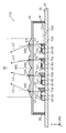
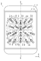
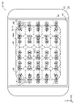
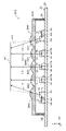
- FIG. 1 is a plan view of a light emitting device according to Embodiment 1.
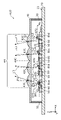
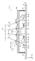
- FIG. 2 is a cross-sectional view of the light-emitting device according to Embodiment 1.
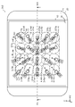
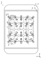
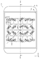
- FIG. 3 is a plan view of the light-emitting device according to Embodiment 1 from which the optical members are removed.
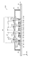
- 4 is a cross-sectional view showing configurations of a semiconductor laser chip, a submount, and a mirror according to Embodiment 1.
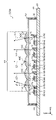
- FIG. 5 is a cross-sectional view illustrating optical paths in the light-emitting device according to Embodiment 1.
- FIG. 6 is a diagram showing a positional relationship between a plurality of mirrors and a plurality of lens units in the light emitting device according to Embodiment 1.
- FIG. 1 is a plan view of a light emitting device according to Embodiment 1.
- FIG. 2 is a cross-sectional view of the light-emitting device according to Embodiment 1.
- FIG. 3 is
- FIG. 7 is a cross-sectional view of a light-emitting device according to Modification 1 of Embodiment 1.
- FIG. 8 is a cross-sectional view of a light-emitting device according to Modification 2 of Embodiment 1.
- FIG. 9 is a plan view showing a state in which the optical member of the light emitting device according to Embodiment 2 is removed.
- 10 is a cross-sectional view of a light-emitting device according to Embodiment 2.
- FIG. 11 is a cross-sectional view of a light-emitting device according to a modification of Embodiment 2.
- FIG. 12 is a plan view showing a state in which the optical member of the light-emitting device according to Embodiment 3 is removed.
- FIG. 13 is a cross-sectional view of a light-emitting device according to Embodiment 3.
- FIG. 14 is a cross-sectional view of a light-emitting device according to a modification of Embodiment 3.
- FIG. 15 is a plan view showing a state in which the optical members are removed from the light-emitting device according to Embodiment 4.
- FIG. 16 is a cross-sectional view of a light-emitting device according to Embodiment 4.
- FIG. 17 is a cross-sectional view of a light-emitting device according to a modification of Embodiment 4.
- FIG. 18 is a plan view of the light-emitting device according to Embodiment 5 from which the optical member is removed.
- FIG. 19 is a cross-sectional view of a light-emitting device according to Embodiment 5.
- FIG. FIG. 20 is a plan view showing a state in which the optical member of the light-emitting device according to Embodiment 6 is removed.
- 21 is a plan view showing a state in which an optical member is removed from a light-emitting device according to a modification of Embodiment 6.
- FIG. 22 is a plan view showing a state in which the optical members of the light emitting device according to Embodiment 7 are removed.
- FIG. 23 is a plan view showing a state in which an optical member is removed from a light-emitting device according to a modification of Embodiment 7.
- FIG. 24 is a plan view showing a state in which the optical member of the light-emitting device according to Embodiment 8 is removed.
- 25 is a schematic cross-sectional view of a light-emitting device according to Embodiment 8.
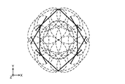
- FIG. 26 is a diagram showing a far-field image in which all output light profiles in a predetermined surface area of the light-emitting device according to Embodiment 8 are superimposed.
- 27 is a schematic cross-sectional view of a light-emitting device according to a modification of Embodiment 8.
- each figure is a schematic diagram and is not necessarily strictly illustrated. Therefore, the scales and the like are not always the same in each drawing.
- symbol is attached
- the terms “upper” and “lower” do not refer to the upward direction (vertically upward) and the downward direction (vertically downward) in absolute spatial recognition, but are based on the stacking order in the stacking structure. It is used as a term defined by a relative positional relationship. Also, the terms “above” and “below” are used not only when two components are spaced apart from each other and there is another component between the two components, but also when two components are spaced apart from each other. It also applies when they are arranged in contact with each other.
- Embodiment 1 A light-emitting device according to Embodiment 1 will be described.
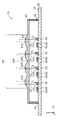
- FIG. 1 and 2 are respectively a plan view and a cross-sectional view of a light emitting device 10 according to this embodiment.
- FIG. 2 shows a cross section taken along line II-II of FIG.
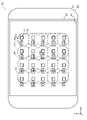
- FIG. 3 is a plan view showing a state in which the optical member 40 is removed from the light emitting device 10 according to this embodiment.
- Each figure also shows an X-axis, a Y-axis, and a Z-axis that are orthogonal to each other.
- the light-emitting device 10 is a device that irradiates light onto a predetermined surface area (not shown) located away from the light-emitting device 10 in the Z direction. 20 , a plurality of semiconductor laser chips 60 , a plurality of mirrors 70 and an optical member 40 .
- light emitting device 10 further includes frame member 30 and a plurality of submounts 50 .
- the base 20 shown in FIGS. 1 to 3 is a member having a main surface 21 on which a plurality of semiconductor laser chips 60 are mounted.
- the base 20 is a substrate having a substantially rectangular plate-like shape.
- the base 20 is made of a material with high thermal conductivity, and also functions as a heat dissipation member that dissipates the heat generated by the plurality of semiconductor laser chips 60 .
- the material of the base 20 is, for example, a metal material, a ceramic material, a glass material, a resin material, or the like.
- the base 20 is preferably made of a material with high thermal conductivity such as a metal material. Examples of metal materials that have high thermal conductivity and are practical for the base 20 include Cu and Al.
- the base 20 is a Cu substrate made of Cu.
- a structure for fixing the base 20 may be formed on a portion of the base 20 outside the frame member 30 or the like.
- a through hole or the like may be formed in the base 20 .
- the frame member 30 shown in FIGS. 2 and 3 is an annular member surrounding multiple semiconductor laser chips 60 and multiple mirrors 70 .
- the frame member 30 is erected on the main surface 21 of the base 20 and functions as a part of a container that houses a plurality of semiconductor laser chips 60 and the like.
- the frame member 30 also has a function of supporting the optical member 40 .
- the frame member 30 is sandwiched between the base 20 and the optical member 40 .
- a plurality of semiconductor laser chips 60 and a plurality of mirrors 70 are accommodated in a space surrounded by the frame member 30 , the base 20 and the optical member 40 .
- the frame member 30 may have current terminals for supplying current to the plurality of semiconductor laser chips 60 .
- the frame member 30 is made of, for example, a metal such as Fe, an alloy, or the like. When the frame member 30 has a current terminal, an insulating member is arranged around the current terminal.
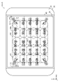
- Each of the plurality of semiconductor laser chips 60 shown in FIGS. 2 and 3 is a semiconductor light-emitting element mounted on the principal surface 21 of the base 20 and having an optical axis parallel to the principal surface 21 .
- each of twenty semiconductor laser chips 60 is mounted on main surface 21 via submount 50 .
- a plurality of semiconductor laser chips 60 are arranged in a matrix in the X-axis direction and the Y-axis direction, as shown in FIG.
- Each of the plurality of semiconductor laser chips 60 is arranged at a position corresponding to each of the plurality of lens portions 43 of the optical member 40 .
- each of the plurality of semiconductor laser chips 60 has an emission point E1 from which emission light L1, which is laser light, is emitted.
- the optical axis of the emitted light L1 is parallel to the main surface 21 of the base 20 .
- the emitted light L1 is indicated by an arrow, and this arrow indicates the optical axis of the emitted light L1, and the actual emitted light L1 is divergent light with a width.
- the semiconductor laser chip 60 has an elongated shape whose longitudinal direction is the optical axis direction (that is, resonance direction) of the emitted light L1.
- the length of the semiconductor laser chip 60 in the optical axis direction is 1200 ⁇ m, but it is not limited to this.
- the semiconductor laser chip 60 is mounted on the top surface of the submount 50 . Specifically, the semiconductor laser chip 60 is mounted on wiring electrodes (not shown) on the submount 50 . In this embodiment, the semiconductor laser chip 60 is mounted on the submount 50 by junction-down mounting. The mounting form of the semiconductor laser chip 60 is not limited to this, and may be mounted on the submount 50 by junction-up mounting.
- the semiconductor laser chip 60 is mounted so that the end face where the emission point E1 is positioned protrudes from the end face of the submount 50 on the light emission side. In other words, the semiconductor laser chip 60 protrudes from the end face of the submount 50, and the emission point E1 of the semiconductor laser chip 60 is positioned closer to the light emission side of the semiconductor laser chip 60 than the end face of the submount 50 on the light emission side. ing.
- the amount of protrusion of the semiconductor laser chip 60 (that is, the distance from the light emitting side end surface of the submount 50 to the emission point E1 of the semiconductor laser chip 60) is, for example, 5 ⁇ m or more and 20 ⁇ m or less, but is not limited thereto. In this embodiment, the amount of projection of the semiconductor laser chip 60 is 10 ⁇ m.
- Each of the plurality of submounts 50 shown in FIGS. 2 to 4 is a member that is mounted on the main surface 21 of the base 20 and supports the semiconductor laser chip 60 .
- the plurality of submounts 50 all have the same configuration.
- the submount 50 has a mounting surface 51 facing the main surface 21 of the base 20, and a mounting surface 52 positioned behind the mounting surface 51 and on which the semiconductor laser chip 60 is mounted.
- the submount 50 is positioned between the base 20 and the semiconductor laser chip 60 .
- the light emitting device 10 has the same number of submounts 50 as the semiconductor laser chips 60 .
- 20 submounts 50 correspond to 20 semiconductor laser chips 60 on a one-to-one basis.
- the submount 50 also functions as a heat sink for dissipating heat generated by the semiconductor laser chip 60. Therefore, the material of the submount 50 may be either a conductive material or an insulating material, but preferably a material with high thermal conductivity.
- the thermal conductivity of the submount 50 is preferably 150 W/(m ⁇ K) or more, for example.
- the submount 50 is made of a ceramic such as aluminum nitride (AlN) or polycrystalline silicon carbide (SiC), a metal material such as Cu, or a single crystal diamond or polycrystalline diamond.
- the submount 50 is made of AlN.
- the shape of the submount 50 is, for example, a rectangular parallelepiped, but is not limited to this.
- the submount 50 is bonded, for example, to the main surface 21 of the base 20 using a metallic bonding material.
- the submount 50 is mounted without forming a fixing hole or the like in the base 20 . Therefore, the submount 50 can be mounted on the base 20 without degrading the heat dissipation characteristics of the base 20 .
- Each of the plurality of mirrors 70 is an element having a reflecting surface 71 that reflects the emitted light L1 from the emission point E1 of each of the plurality of semiconductor laser chips 60, as shown in FIG.
- the multiple mirrors 70 all have the same configuration.
- a plurality of mirrors 70 are arranged in a matrix in the X-axis direction and the Y-axis direction, as shown in FIG.
- Each of the plurality of mirrors 70 is arranged at a position corresponding to each of the plurality of lens portions 43 of the optical member 40 .
- the reflecting surface 71 is a plane mirror arranged to face the emission point E1 of the semiconductor laser chip 60 .
- the reflecting surface 71 is inclined at 45° with respect to the direction of the emitted light L1.
- the direction perpendicular to the reflecting surface 71 is inclined at 45° with respect to the direction of the emitted light L1.
- the emitted light L1 is reflected by the reflecting surface 71 and propagates from the mirror 70 toward the optical member 40 as reflected light L2.
- emitted light L1 is incident on center position 71C of reflecting surface 71 shown in FIG.
- the center position 71C of the reflecting surface 71 is defined by the center-of-gravity position of the reflecting surface 71 .
- the reflected light L2 is indicated by an arrow, but this arrow indicates the optical axis of the reflected light L2, and the actual reflected light L2 is divergent light with a width.
- the mirror 70 is mounted on the main surface 21 of the base 20.
- the light-emitting device 10 includes the same number of mirrors 70 as there are semiconductor laser chips 60 .
- 20 mirrors 70 correspond to 20 semiconductor laser chips 60 on a one-to-one basis.
- all sets of the mirror 70 and the semiconductor laser chip 60 have the same positional relationship.
- the distances from the emission point E1 of the semiconductor laser chip 60 to the center position C1 of the emission light L1 on the reflecting surface 71 are all the same, and the height of the optical axis of the emission light L1 of the semiconductor laser chip 60 from the main surface 21 is the same.
- the height from the main surface 21 of the sheath reflective surface 71 is all the same.
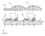
- the optical member 40 shown in FIGS. 1, 2, and 4 is a translucent plate member having a plurality of lens portions 43. As shown in FIG. The optical member 40 is supported by the frame member 30 and also functions as a lid for the area surrounded by the frame member 30 . Each of the plurality of lens portions 43 receives reflected light L2 from each reflecting surface 71 of each of the plurality of mirrors 70, as shown in FIG. In this embodiment, all of the multiple lens units 43 have the same focal length.
- the lens portion 43 is, for example, a spherical lens.
- the surface of the lens portion 43 facing the reflecting surface 71 is flat, and the surface on the back side (that is, outside) of the surface has a spherical convex shape.
- the lens portion 43 is a convex lens.
- the optical member 40 has the same number of lens portions 43 as the semiconductor laser chips 60 and the mirrors 70 .
- the plurality of lens units 43 are arranged in a matrix in the X-axis direction and the Y-axis direction, as shown in FIG.
- Each of the plurality of lens units 43 is arranged at a position corresponding to each of the plurality of mirrors 70 .
- 20 lens units 43 correspond to 20 mirrors 70 on a one-to-one basis.
- the optical member 40 is made of, for example, a translucent member such as glass.
- the optical member 40 has a lens region 44 in which a plurality of lens portions 43 are arranged, as shown in FIG.
- the lens region 44 is, for example, a region surrounded by an envelope 44E of the multiple lens portions 43 .
- a center position 44C of the lens area 44 is the center of gravity of the lens area 44 .
- FIG. 5 is a cross-sectional view illustrating optical paths in the light emitting device 10 according to this embodiment.
- FIG. 5 shows a partially enlarged view of a section similar to that of FIG. 2 and an optical path.
- FIG. 6 is a diagram showing the positional relationship between the multiple mirrors 70 and the multiple lens units 43 in the light emitting device 10 according to the present embodiment.
- FIG. 6 shows a plan view of the main surface 21 of the base 20 in plan view. In FIG. 6, the contours of the plurality of lens portions 43 are also shown by dashed lines.
- emitted light L1 emitted from the semiconductor laser chip 60 and having an optical axis parallel to the main surface 21 is reflected by the reflecting surface 71 of the mirror 70 and travels toward the lens portion 43 as reflected light L2.
- the direction of the optical axis of the reflected light L2 is parallel to the direction perpendicular to the main surface 21 of the base 20 .
- the reflected light L2 is incident on the lens portion 43 .
- the direction of the optical axis of the lens portion 43 is parallel to the direction perpendicular to the main surface 21 of the base 20 .
- the lens part 43 makes the reflected light L2, which is divergent light, in a parallel state or a converged state, and is output from the light emitting device 10 as the output light L3.
- the output light L3 from the lens portion 43 is directed in the optical axis direction of the lens portion 43. refract.
- the output light L3 is indicated by an arrow, this arrow indicates the optical axis of the output light L3, and the actual output light L3 has a width.
- the lens portion corresponding to the reflecting surface 71 among the plurality of lens portions 43 The following relationship holds for the distance in the X-axis direction to the center position 43C of 43 (hereinafter also referred to as first distance Dc).
- the distance Dc to the lens portion 43 located at the outermost side of the lens region 44 among the plurality of lens portions 43 is greater than the distance Dc to the lens portion 43 closest to the center position 44C of the lens region 44 among the plurality of lens portions 43. is large.
- the distance Dc increases as the distance (De) in the X-axis direction between the center position C1 of the emitted light L1 and the center position 44C of the lens region 44 where the plurality of lens portions 43 are arranged increases. so it gets bigger.
- the center position C1 of the emitted light L1 on the reflecting surface 71 is defined by the center position of the beam profile of the emitted light L1 or the position where the intensity of the emitted light L1 is maximized.
- a center position 43C of the lens portion 43 is defined at a position through which the optical axis of the lens portion 43 (one-dot chain line shown in FIG. 5) passes in plan view of the main surface 21 . Although no auxiliary line is shown in the drawing, the center position C1 of the emitted light L1 on the reflecting surface 71 also changes in the Y-axis direction as well.
- the X-axis direction from the center position 71C of the reflecting surface 71 to the center position 43C of the lens portion 43 corresponding to the reflecting surface 71 among the plurality of lens portions 43 in plan view of the main surface 21 The following relationship holds for the distance (hereinafter also referred to as the second distance).
- the second distance to the lens portion 43 that is located on the outermost side of the lens region 44 among the plurality of lens portions 43 is greater than the second distance to the lens portion 43 that is the closest to the center position 44C of the lens region 44 among the plurality of lens portions 43 .
- distance is greater.
- the second distance increases as the distance in the X-axis direction between the center position 71C of the reflecting surface 71 and the center position 44C of the lens area 44 increases.
- the center position C1 of the emitted light L1 on the reflecting surface 71 and the center position 71C of the reflecting surface 71 match. Note that the center position C1 of the emitted light L1 on the reflecting surface 71 and the center position 71C of the reflecting surface 71 do not have to match.
- the output light L3 from each of the plurality of lens portions 43 is irradiated inside the predetermined surface area A1 having an area smaller than that of the lens area 44.
- the predetermined surface area A1 having a smaller area than the lens area 44 is provided with no condensing lens between the optical member 40 and the predetermined surface area A1.
- a plurality of output lights L3 can be collected.
- the optical axes of all the output light beams L3 can be gathered in one place.
- the central position 71C of the reflecting surface 71 also changes in the Y-axis direction.
- the center position 43C of the lens portion 43 is on the line segment connecting the center position C1 of the emitted light L1 and the center position 44C of the lens region 44, but it is not necessarily strictly on the line segment. It doesn't have to be.
- the direction of the optical axis of each output light L3 is generally directed toward the center position of the lens region 44 in plan view, it does not necessarily have to be directed strictly toward the center position.
- the distance from the emission point E1 of the semiconductor laser chip 60 to the central position C1 of the emitted light L1 on the reflecting surface 71 is all the same.
- the effect of changes in the positions of the semiconductor laser chip 60 and the mirror 70 on the convergence state of the output light L3 can be greatly reduced.
- the center position C1 of the emitted light L1 on the reflecting surface 71 and the center position 71C of the reflecting surface 71 coincide with each other, the emitted light L1 can be efficiently reflected by the mirror 70 .
- the output light L3 is projected onto the predetermined surface region A1 having a smaller area than when the output light L3 is not a condensed beam. can be collected. In other words, the area of the far-field pattern formed by the multiple output lights L3 can be reduced. Therefore, it is possible to further increase the light density in the predetermined surface area A1.
- Light-emitting device 10 includes a plurality of semiconductor laser chips 60, as shown in FIG.
- Each of the plurality of semiconductor laser chips 60 is mounted on main surface 21 of base 20 and has an optical axis parallel to main surface 21 .
- a semiconductor laser chip 60 is mounted on the main surface 21 via a submount 50 .
- the submount 50 can be mounted without forming a fixing hole or the like in the base 20 , the submount 50 can be mounted on the base 20 without degrading the heat dissipation characteristics of the base 20 .
- the semiconductor laser chip 60 can be mounted on the base 20 only through the submount 50 .
- the semiconductor laser chip 60 can be mounted at a position close to the main surface 21 of the base 20 . Therefore, by using the submount 50 with high thermal conductivity, the heat radiation characteristic from the semiconductor laser chip 60 to the base 20 can be improved compared to the case where a CAN package including the semiconductor laser chip 60 is mounted on the base 20. can be done. As described above, according to the present embodiment, it is possible to realize the light emitting device 10 capable of improving the heat dissipation characteristics of the plurality of semiconductor laser chips 60 .
- the semiconductor laser chip 60 is mounted on each of the multiple submounts 50 .
- the semiconductor laser chip 60 is bonded to the mounting surface 52 of the submount 50 using a metallic bonding material.
- a Zener diode for maintaining a constant voltage supplied to the semiconductor laser chip 60 may also be joined to the mounting surface 52 of the submount 50 .
- the metallic bonding material for example, solder materials such as AuSn and AuGeNi, and bonding materials containing fine particles of Cu, Al, Au, Ag, and alloys thereof can be used.
- the submount 50 with the semiconductor laser chip 60 mounted thereon is mounted on the main surface 21 of the base 20 .
- the submount 50 is bonded to the main surface 21 of the base 20 using a metallic bonding material.
- the metallic bonding material for example, solder materials such as AuSn and AuGeNi, and bonding materials containing fine particles of Cu, Al, Au, Ag, and alloys thereof can be used.
- the submount 50 can be mounted on the base 20 .
- the frame member 30 is mounted on the base 20 in advance. Also, the frame member 30 may be formed integrally with the base 20 .
- a wire for supplying current to the semiconductor laser chip 60 is connected to the semiconductor laser chip 60 and the like.
- the terminals provided on the frame member 30 and the semiconductor laser chips 60 are connected by wires, and two adjacent semiconductor laser chips 60 are connected in series by wires.
- current can be supplied from the outside of the light emitting device 10 .
- the wire material is not particularly limited as long as it is conductive, and examples thereof include Au, Ag, and Cu.
- the mirror 70 is mounted on the main surface 21 of the base 20. Specifically, the mirror 70 is bonded to the main surface 21 of the base 20 using a metallic bonding material. Active alignment of the mirror 70 is performed before curing the metallic bonding material. In other words, a current is supplied to the semiconductor laser chip 60 to emit the emitted light L1, and while confirming the position of the emitted light L1 on the reflecting surface 71 of the mirror 70 and the position of the reflected light L2 from the mirror 70, The position of the mirror 70 on the main surface 21 is adjusted. After the alignment of the mirror 70 is completed, the metallic bonding material is cured in the same manner as when the submount 50 is mounted. Thereby, the mirror 70 can be mounted on the base 20 .
- the optical member 40 is mounted on the base 20.
- the optical member 40 is mounted on the base 20 via the frame member 30 .
- the optical member 40 is bonded to the frame member 30 using an adhesive or the like.
- the adhesive for example, a UV curable adhesive can be used.
- a UV curable adhesive is applied to at least one of the frame member 30 and the optical member 40 to temporarily fix the optical member 40 .
- active alignment of the positions of the optical member 40 in the X-, Y-, and Z-axis directions is performed.
- the UV curable adhesive is cured by irradiating it with UV light. Thereby, the optical member 40 can be mounted on the base 20 .
- the light emitting device 10 can be manufactured.
- a translucent member such as a cover glass may be attached between the optical member 40 and the frame member 30 .
- the plurality of lens portions 43 of the optical member 40 may be configured to be separable from the optical member 40 . In this case, the plurality of lens units 43 may be actively aligned individually.
- FIG. 7 and 8 are cross-sectional views of light-emitting devices according to modified examples 1 and 2 of the present embodiment, respectively.
- the plurality of lens portions 43 are arranged from the center position C1 of the emitted light L1 on the reflecting surface 71 in plan view of the main surface 21 .
- the distance (first distance) to the center position 43C of the lens portion 43 corresponding to the reflecting surface 71 is growing.
- the distance (second distance) from the center position 71C of the reflecting surface 71 to the center position 43C of the lens portion 43 corresponding to the reflecting surface 71 among the plurality of lens portions 43 in plan view of the main surface 21 is It increases as the distance from the center position 71C of the surface 71 to the center position 44C of the lens area 44 increases.
- the reflected light L2 incident on the left and right end lens portions 43 is emitted from the lens portion 43 as output light L3 having an optical axis inclined in a direction toward the center position 44C of the lens region 44 with respect to the optical axis of the reflected light L2. output. Therefore, according to the light emitting device 10A according to Modification 1 of the present embodiment, by appropriately selecting the irradiation distance from the lens region 44 to the predetermined surface region A1, the predetermined surface region A1 narrower than the lens region 44 has a plurality of light beams. Output light L3 can be emitted.
- the predetermined lens area having a smaller area than the lens area 44 is not arranged between the optical member 40 and the predetermined surface area A1.
- a plurality of output lights L3 can be condensed on the surface area A1.
- the distance and the second distance are zero.
- the first distance and the second distance are values other than zero in the left end and right end lens portions 43 among the plurality of lens portions 43 .
- the optical axis of the reflected light L2 is located outside the lens area 44 (farther from the center position 44C) than the center position 43C of the lens portion 43.
- the first distance and the second distance are is about 1/10 of the first distance and the second distance with respect to the lens portion 43 of .
- the optical axis of the reflected light L2 corresponding to the lens portion 43 is located inside the lens area 44 ( position close to the center position 44C).
- the first distance and the second distance are is about 1/10 of the first distance and the second distance with respect to the lens portion 43 of .
- the optical axis of the reflected light L2 corresponding to the lens portion 43 is positioned closer to the lens region 44 than the center position 43C of the lens portion 43 located between the center lens portion 43 and the right end lens portion 43. It is located inside (a position close to the center position 44C).
- the reflected light L2 incident on the lens portion 43 closest (center) to the center position 44C of the lens region 44 is parallel to the reflected light L2 without substantially being refracted. It is output from the lens portion 43 as propagating output light L3.
- the reflected light L2 incident on the two lens portions 43 between the center and the left and right ends is output from the lens portion 43 as output light L3 having an optical axis slightly inclined away from the center position 44C of the lens area 44. be.
- the reflected light L2 incident on the lens portions 43 at the left and right ends is output from the lens portion 43 as output light L3 having an optical axis inclined toward the center position 44C of the lens region 44 with respect to the optical axis of the reflected light L2.
- the relationship between the center position 71C of the reflecting surface 71 of the mirror 70 and the center position 43C of the lens portion 43 of the light emitting device according to the present embodiment is not limited to the relationship in the light emitting device 10 described above. That is, the first distance to the lens portion 43 that is closest to the center position 44C of the lens region 44 among the plurality of lens portions 43 is greater than the first distance to the lens portion 43 that is positioned on the outermost side of the lens region 44 among the plurality of lens portions 43 . The first distance should be larger.
- the second distance to the lens portion 43 that is closest to the center position 44C of the lens region 44 among the plurality of lens portions 43 is longer than the second distance to the lens portion 43 that is positioned on the outermost side of the lens region 44 among the plurality of lens portions 43 .
- the second distance should be larger.
- the first distance to all the lens portions 43 located on the outermost side of the lens region 44 may not be larger than the first distance to the lens portion 43 closest to the center position 44C of the lens region 44. , the first distance from at least one of the lens portions 43 located on the outermost side of the lens area 44 should be larger.
- the second distance to all of the lens portions 43 located on the outermost side of the lens region 44 may not be greater than the second distance to the lens portion 43 closest to the center position 44C of the lens region 44. , the second distance from at least one of the lens portions 43 located on the outermost side of the lens area 44 should be larger.
- Embodiment 2 A light-emitting device according to Embodiment 2 will be described.
- the positions of the mirror 70 and the semiconductor laser chip 60 with respect to the lens portion 43 are adjusted according to the distance from the center position 44C of the lens region 44 to the center position 71C of the reflecting surface 71 of the mirror 70. While maintaining the relationship, the position in the plane view was changed.
- the light emitting device according to the present embodiment does not change the positions of the mirror 70 and the semiconductor laser chip 60 with respect to the lens portion 43, but changes the height of the optical axis of the emitted light L1 from the main surface 21 of the base 20.
- Embodiment 1 It is different from the light-emitting device 10 according to Embodiment 1 in that The light-emitting device according to the present embodiment will be described below with reference to FIGS. 9 and 10, focusing on differences from the light-emitting device 10 according to the first embodiment.
- FIG. 9 is a plan view showing a state in which the optical member 40 is removed from the light emitting device 110 according to this embodiment.
- FIG. 9 shows a plan view of the main surface 21 of the base 20 in plan view.
- the contours of the plurality of lens portions 43 are also shown by dashed lines.
- FIG. 10 is a cross-sectional view of light emitting device 110 according to this embodiment.
- FIG. 10 shows a cross section along line XX in the X-axis direction of FIG. Note that FIG. 10 also shows a cross section of the optical member 40 .
- the light emitting device 110 includes a base 20, a frame member 30, an optical member 40, a plurality of semiconductor laser chips 60, a plurality of submounts 53a to 53d, 54a to 54d, 55a to 55d, 56a-56d, 57a-57d and a plurality of mirrors 70 are provided.
- the relative positions of each of the plurality of mirrors 70 and each of the plurality of lens portions 43 in plan view of the main surface 21 of the base 20 are all the same. Same for mirror 70 .
- the center position 43C of each of the plurality of lens portions 43 and the center position of the reflecting surface 71 corresponding to each of the plurality of lens portions 43 71C matches.
- the distances from the emission point E1 of the semiconductor laser chip 60 to the center position 71C of the reflecting surface 71 are all the same. In other words, the positional relationship between the semiconductor laser chip 60 and the mirror 70 is the same.
- the plurality of submounts 53a to 53d, 54a to 54d, 55a to 55d, 56a to 56d, and 57a to 57d differ from the submount 50 according to Embodiment 1 in that they are different in height. different.
- the direction of the optical axis of the reflected light L2 is parallel to the direction perpendicular to the main surface 21 because the angle of the reflecting surface with respect to the main surface is 45°.
- the difference between the height from the main surface 21 to the emission point E1 of each of the plurality of semiconductor laser chips 60 and the average value Ha1 of the heights from the main surface 21 to the emission point E1 of each of the plurality of semiconductor laser chips 60 The following relationship holds for the absolute value (hereinafter also referred to as the first difference D1). Outermost of the lens area 44 among the plurality of lens sections 43 than the first difference D1 with respect to the emission point E1 corresponding to the lens section 43 closest to the center position 44C of the lens area 44 among the plurality of lens sections 43 The first difference D1 with respect to the emission point E1 corresponding to the lens portion 43 corresponding to the corresponding lens portion 43 is larger.
- the first difference D1 increases as the distance from the center position 44C of the lens region 44 to the center position 43C of the lens portion 43 corresponding to each of the plurality of submounts among the plurality of lens portions 43 increases. Become. Therefore, the distance of the optical axis of the semiconductor laser chip 60 from the main surface 21, that is, the position of the emitted light L1 on the reflecting surface 71 in the X-axis direction varies depending on the height of the submount.
- a plurality of The distance in the X-axis direction from the center position C1 of the emitted light L1 to the center position 43C of the lens part 43 corresponding to the reflecting surface 71 is the lens area 44 where the plurality of lens parts 43 are arranged. increases as the distance in the X-axis direction to the center position 44C of the increases. Therefore, the position of the reflected light L2 incident on each of the plurality of lens portions 43 according to the present embodiment is the same as in the first embodiment in the X-axis direction, and the output light L3 is reflected in the lens area 44 in the X-axis direction.
- each output light L3 is generally directed to the central position of the lens region 44 in the X-axis direction in a plan view, but it is not necessarily strictly directed. It doesn't have to be.
- the plurality of output lights L3 can be condensed on the predetermined surface area A1 having an area smaller than that of the lens area 44 without arranging a condensing lens.
- a plurality of output light beams L3 can be condensed on a predetermined surface region A1 having an area smaller than that of the lens region 44 without arranging a condensing lens.
- the main surface 21 of the base 20 parallel to the emitted light L1 and the reflecting surface 71 is 45°, even if the height from the main surface 21 to the position of the emission point E1 of the semiconductor laser chip 60 changes, the emission from the emission point E1 of the semiconductor laser chip 60 on the reflecting surface 71
- the sum of the distance to the center position of the emitted light L1 and the distance from the center position of the emitted light L1 on the reflecting surface 71 to the lens portion 43 is constant, and the height from the main surface 21 to the position of the emission point E1 of the semiconductor laser chip 60 is constant. It is possible to greatly reduce the influence of the light intensity on the convergence state of the output light L3.
- each of the plurality of semiconductor laser chips 60 is mounted on main surface 21 and , the same effect of improving heat dissipation characteristics as the light emitting device 10 according to the first embodiment can be obtained.
- FIG. 11 is a cross-sectional view of a light emitting device 110A according to this modification.
- the difference (first difference D1) between the average value Ha1 of the heights up to the emission point E1 of each of the plurality of semiconductor laser chips 60 is the emission point of the plurality of lens portions 43 from the center position 44C of the lens region 44. It increases as the distance to the center position 43C of the lens portion 43 corresponding to E1 increases.
- the light-emitting device 110A as shown in FIG. has a first difference D1 of zero.
- the first difference is not zero in the lens portions 43 located on the outermost side of the lens area 44 among the plurality of lens portions 43 (the leftmost and rightmost lens portions 43 in FIG. 11).
- the reflected light L2 incident on the left and right end lens portions 43 is emitted from the lens portion 43 as output light L3 having an optical axis inclined in a direction toward the center position 44C of the lens region 44 with respect to the optical axis of the reflected light L2. output. Therefore, according to the light emitting device 110A according to this modified example, by appropriately selecting the irradiation distance from the lens region 44 to the predetermined surface region A1, the predetermined surface region A1 narrower than the lens region 44 is irradiated with the plurality of output light beams L3. can do.
- a plurality of condenser lenses are not disposed between the optical member 40 and the predetermined surface area A1, and the predetermined surface area A1 having an area smaller than that of the lens area 44 has a plurality of lenses.
- output light L3 can be condensed.
- the relationship between the center position of the emitted light L1 of the light emitting device according to the present embodiment and the center position 43C of the lens portion 43 is not limited to the relationship in the light emitting device 110 described above. That is, the outermost position of the lens region 44 among the plurality of lens portions 43 is greater than the first difference D1 with respect to the emission point E1 corresponding to the lens portion 43 closest to the center position 44C of the lens region 44 among the plurality of lens portions 43 . It is sufficient if the first difference D1 with respect to the emission point E1 corresponding to the lens portion 43 located at is larger.
- the first difference for all the emission points E1 corresponding to the lens portions 43 located on the outermost side of the lens region 44 is greater than the first difference for the emission points E1 corresponding to the lens portions 43 closest to the center position 44C of the lens region 44.
- the first difference D1 does not have to be large, and the first difference D1 with respect to at least one emission point E1 corresponding to the lens portion 43 located on the outermost side of the lens area 44 may be larger.
- Embodiment 3 A light-emitting device according to Embodiment 3 will be described.
- the height of the optical axis of the emitted light L1 from the main surface 21 is the same for all the semiconductor laser chips 60, and the height of the reflecting surface 71 from the main surface 21 is changed. It differs from the light emitting device 110 according to Embodiment 2 in that the distance between the emission point E1 and the center position 71C of the reflecting surface 71 is changed in plan view.
- the light emitting device according to the present embodiment will be described below with reference to FIGS. 12 and 13, focusing on differences from the light emitting device 110 according to the second embodiment.
- FIG. 12 is a plan view showing a state in which the optical member 40 is removed from the light emitting device 210 according to this embodiment.
- FIG. 12 shows a plan view of the main surface 21 of the base 20 in plan view.
- the contours of the plurality of lens portions 43 are shown together with dashed lines.
- FIG. 13 is a cross-sectional view of light emitting device 210 according to this embodiment.
- FIG. 13 shows a cross section along line XIII-XIII of FIG. Note that FIG. 13 also shows a cross section of the optical member 40 .
- a light emitting device 210 includes a base 20, a frame member 30, an optical member 40, a plurality of semiconductor laser chips 60, a plurality of submounts 50, a plurality of mirrors 73a-73d, 74a- 74d, 75a-75d, 76a-76d, 77a-77d.
- the multiple submounts 50 according to the present embodiment have the same configuration as the multiple submounts 50 according to the first embodiment. Therefore, the distances of the optical axes of the semiconductor laser chips 60 mounted on the plurality of submounts 50 from the main surface 21 are all the same.
- Each of the plurality of mirrors 73a to 73d, 74a to 74d, 75a to 75d, 76a to 76d, and 77a to 77d has a reflecting surface 71 like the mirror 70 according to the second embodiment.
- the relative positions of each of the plurality of mirrors and each of the plurality of lens portions 43 are the same for all mirrors.
- the center position 43C of each of the plurality of lens portions 43 and the center position of the reflecting surface 71 corresponding to each of the plurality of lens portions 43 71C matches.
- the heights of the central position 71C of the reflecting surface 71 from the main surface 21 are not the same. different from The direction of the optical axis of the reflected light L2 is parallel to the direction perpendicular to the main surface 21 because the angle of the reflecting surface 71 with respect to the main surface 21 is 45°.
- the absolute value of the difference between the height from the main surface 21 to the center position 71C of the reflecting surface 71 and the average value Ha2 of the heights from the main surface 21 to the center position 71C of the reflecting surface 71 at a plurality of mirrors (hereinafter referred to as second difference D2), the following relationship holds: Out of the plurality of lens portions 43, the outermost portion of the lens region 44 is positioned more than the second difference D2 with respect to the reflecting surface 71 corresponding to the lens portion 43 closest to the center position 44C of the lens region 44 among the plurality of lens portions 43.
- the second difference D2 with respect to the reflecting surface 71 corresponding to the lens portion 43 corresponding to the second difference D2 is larger.
- the second difference D2 increases as the distance from the center position 44C of the lens region 44 to the center position 43C of the lens portion 43 corresponding to each of the plurality of mirrors among the plurality of lens portions 43 increases. . Therefore, the position of the emitted light L1 on the reflecting surface 71 in the X-axis direction differs depending on the height of the central position 71C of the reflecting surface 71 from the main surface 21 .
- a plurality of The distance from the center position C1 of the emitted light L1 to the center position 43C of the lens area 44 where the plurality of lens parts 43 are arranged is increases as the distance to Therefore, the position of the reflected light L2 incident on each of the plurality of lens portions 43 according to the present embodiment is the same as in the first embodiment in the X-axis direction, and the output light L3 is reflected in the lens area 44 in the X-axis direction. refracts toward the center of On the other hand, there is no bending in the Y-axis direction.
- the direction of the optical axis of each output light L3 is roughly directed to the central position of the lens region 44 in the X-axis direction in a plan view, but it is not necessarily strictly directed. It doesn't have to be. Therefore, in the light-emitting device 210 according to the present embodiment as well, the plurality of output lights L3 can be condensed onto the predetermined surface area A1 having an area smaller than that of the lens area 44 without arranging a condensing lens.
- the absolute value of the difference from the average height of the reflecting surface 71 to the center position 71C is proportional to De, so that the optical axis of all the output light beams L3 is approximately 1 or 1. can be collected in place.
- the angle formed by the emitted light L1 and the reflecting surface 71 is 45°, the emitted light L1 on the reflecting surface 71 is equal to the amount of change in height from the main surface 21 to the center position 71C of the reflecting surface 71.
- the distance from the center position of the to the lens portion 43 is shortened. Therefore, as shown in FIG.
- FIG. 14 is a cross-sectional view of a light emitting device 210A according to this modification.
- the second difference D2 is zero.
- the second difference D2 is not zero in the lens portions 43 (the leftmost and rightmost lens portions 43 in FIG. 14) located on the outermost side of the lens area 44 among the plurality of lens portions 43 .
- the reflected light L2 incident on the three central lens portions 43 is output from the lens portions 43 as three output light beams L3 whose optical axes are parallel to each other.
- the reflected light L2 incident on the left and right end lens portions 43 is emitted from the lens portion 43 as output light L3 having an optical axis inclined in a direction toward the center position 44C of the lens region 44 with respect to the optical axis of the reflected light L2. output. Therefore, according to the light emitting device 210A according to this modified example, by appropriately selecting the irradiation distance from the lens area 44 to the predetermined surface area A1, the predetermined surface area A1 narrower than the lens area 44 is irradiated with the plurality of output light beams L3. can do.
- a plurality of condenser lenses are not disposed between the optical member 40 and the predetermined surface area A1, and the predetermined surface area A1 having an area smaller than that of the lens area 44 has a plurality of lenses.
- output light L3 can be condensed.
- the relationship between the position of the optical axis of the reflected light L2 of the light emitting device according to the present embodiment and the center position 43C of the lens portion 43 is not limited to the relationship in the light emitting device 210 described above. That is, the second difference D2 with respect to the reflecting surface 71 corresponding to the lens portion 43 closest to the center position 44C of the lens region 44 among the plurality of lens portions 43 is greater than the outermost portion of the lens region 44 among the plurality of lens portions 43 . It is sufficient if the second difference D2 with respect to the reflecting surface 71 corresponding to the lens portion 43 located at is larger.
- All of the reflecting surfaces 71 corresponding to the lens portion 43 located on the outermost side of the lens region 44 are larger than the second difference D2 with respect to the reflecting surface 71 corresponding to the lens portion 43 closest to the center position 44C of the lens region 44. It is not necessary that the second difference D2 with respect to .theta.
- Embodiment 4 A light-emitting device according to Embodiment 4 will be described.
- the light emitting device according to the present embodiment differs from the light emitting device 10 according to Embodiment 1 mainly in that the direction of the optical axis of at least part of the reflected light L2 is different from the direction of the optical axis of the lens portion 43. differ.
- the light emitting device according to the present embodiment will be described below with reference to FIGS. 15 and 16, focusing on differences from the light emitting device 10 according to the first embodiment.
- FIG. 15 is a plan view showing a state in which the optical member 40 is removed from the light emitting device 310 according to this embodiment.
- FIG. 15 shows a plan view of the main surface 21 of the base 20 in plan view.
- the contours of the plurality of lens portions 43 are shown together with dashed lines.
- FIG. 16 is a cross-sectional view of light emitting device 310 according to this embodiment.
- FIG. 16 shows a cross section along line XVI--XVI of FIG. Note that FIG. 16 also shows a cross section of the optical member 40 .
- a light emitting device 310 includes a base 20, a frame member 30, an optical member 40, a plurality of semiconductor laser chips 60, a plurality of submounts 50, a plurality of mirrors 373a to 373d, 374a to 374d, 375a-375d, 376a-376d, 377a-377d.
- the direction perpendicular to the reflecting surface 71 of each mirror is projected onto the main surface 21 (for example, the direction of the dashed arrow 71D shown in the mirror 374b in FIG. 15).
- each mirror is arranged so as to be in a direction parallel to a two-dot chain line connecting
- the direction of the optical axis of the emitted light L1 from each semiconductor laser chip 60 is such that the direction perpendicular to the reflection surface 71 on which the emitted light L1 is incident coincides with the direction projected onto the main surface 21. and a submount 50 are arranged.
- Each of the plurality of mirrors according to the present embodiment has a reflecting surface 71 like the mirror 70 according to the first embodiment.
- the plurality of mirrors according to the present embodiment are the same as those in the first embodiment in that the optical axis of the reflected light L2 passes through the optical center of the lens portion 43.
- the tilt differs from the mirror 70 according to the first embodiment.
- the angle formed by the direction Dm perpendicular to the main surface 21 and the direction D71 perpendicular to the reflecting surface 71 see the angle ⁇ r at the mirror 375a in FIG. 16
- the average of the angles formed by the plurality of mirrors The following relationship holds for the absolute value of the difference from the value (hereinafter also referred to as the third difference).
- the third difference with respect to the reflecting surface 71 corresponding to the lens portion 43 is larger.
- the third difference increases as the distance from the center position 44C of the lens region 44 to the center position 43C of the lens portion 43 corresponding to the reflecting surface 71 among the plurality of lens portions 43 increases.
- the angle formed by the direction of the optical axis of the reflected light L2 and the direction perpendicular to the main surface 21 (or the direction of the optical axis of the lens portion 43) (hereinafter also referred to as the first angle (see angle ⁇ 1 in FIG. 16) ))))
- the first angle (see angle ⁇ 1 in FIG. 16) ))
- the following relationship holds: Positioned on the outermost side of the lens region 44 among the plurality of lens portions 43 than the first angle ⁇ 1 with respect to the reflected light L2 corresponding to the lens portion 43 closest to the center position 44C of the lens region 44 among the plurality of lens portions 43
- the first angle ⁇ 1 with respect to the reflected light L2 corresponding to the lens portion 43 is larger.
- the first angle ⁇ 1 increases as the distance from the center position 44C of the lens region 44 to the center position 43C of the lens portion 43 that receives the reflected light L2 among the plurality of lens portions 43 increases.
- the optical axis of the reflected light L2 passes through the center position (optical center) of the lens portion 43, so that the optical axis of the lens portion 43 and the optical axis of the reflected light L2
- the reflected light L2 and the output light L3 propagate in the same direction even if there is a deviation.
- the optical axis of the output light L3 is tilted with respect to the optical axis of the lens portion 43 without refracting the optical axis of the reflected light L2 by the lens portion 43, and the output light L3 is focused on the predetermined surface area A1.
- the optical axis of the reflected light L2 does not need to be refracted by the lens portion 43, so that the reflected light L2 can enter the vicinity of the optical axis of the lens portion 43. Therefore, since the coma aberration of the output light L3 can be reduced, distortion of the profile of the output light L3 in the predetermined surface area A1 can be suppressed. That is, the output light L3 can be reliably focused on the predetermined surface area A1.
- the absolute value of the difference from the average value of the formed angles is proportional to the distance from the center position 44C of the lens region 44 to the center position 43C of the lens portion 43, so that the optical axis of all the output light L3 is It can be collected in almost one place.
- the directions of the optical axes of the reflected light beams L2 and the output light beams L3 are generally directed toward the central position of the lens area 44 in a plan view, but they are not necessarily strictly aligned. It does not have to be facing the center position.
- the angle formed by the direction perpendicular to the reflecting surface 71 projected onto the main surface 21 and the incident direction of the emitted light L1 onto the reflecting surface 71 is the same angle.
- the angle is 0°.
- the sum of the distance from the emission point E1 of the semiconductor laser chip 60 to the central position of the emitted light L1 on the reflecting surface 71 and the distance from the central position of the emitted light L1 on the reflecting surface 71 to the lens portion 43 is constant.
- FIG. 17 is a cross-sectional view of a light emitting device 310A according to this modification.
- the absolute value (third difference) of the difference from the average value of the angles formed by the mirror is obtained from the center position 44C of the lens region 44 to the center of the lens portion 43 corresponding to the reflecting surface 71 among the plurality of lens portions 43. It increases as the distance to position 43C increases. Further, the angle (first angle ⁇ 1) formed by the direction of the optical axis of the reflected light L2 and the direction perpendicular to the main surface 21 is determined from the center position 44C of the lens region 44 by the reflected light L2 among the plurality of lens portions 43. increases as the distance to the center position 43C of the lens portion 43 that receives the distance increases.
- the light-emitting device 310A as shown in FIG. is zero for the third difference and the first angle. Further, the third difference and the first angle are not zero in the lens portions 43 (the leftmost and rightmost lens portions 43 in FIG. 17) located on the outermost side of the lens area 44 among the plurality of lens portions 43 .
- the reflected light L2 incident on the three central lens portions 43 is output from the lens portions 43 as three output light beams L3 whose optical axes are parallel to each other.
- the reflected light L2 incident on the left and right end lens portions 43 is output from the lens portion 43 as output light L3 having an optical axis inclined toward the center position 44C of the lens area 44 .
- the predetermined surface region A1 narrower than the lens region 44 is irradiated with the plurality of output light beams L3. can do.
- a plurality of condenser lenses are not disposed between the optical member 40 and the predetermined surface area A1, and the predetermined surface area A1 having an area smaller than the lens area 44 has a plurality of lenses.
- output light L3 can be condensed.
- the relationship between the distance from the center position 44C of the lens region 44 of the lens portion 43 of the light emitting device according to the present embodiment and the inclination of the reflecting surface 71 corresponding to the lens portion 43 is the same as that of the light emitting device 310 described above. is not limited to the relationship in That is, the outermost portion of the lens region 44 among the plurality of lens portions 43 is closer to the reflecting surface 71 than the third difference with respect to the reflecting surface 71 corresponding to the lens portion 43 closest to the center position 44C of the lens region 44 among the plurality of lens portions 43 .
- the third difference with respect to the reflecting surface 71 corresponding to the lens portion 43 located should be larger.
- the outermost angle of the lens region 44 among the plurality of lens portions 43 is greater than the first angle ⁇ 1 with respect to the reflected light L2 corresponding to the lens portion 43 closest to the center position 44C of the lens region 44 among the plurality of lens portions 43 . It is sufficient if the first angle ⁇ 1 with respect to the reflected light L2 corresponding to the lens portion 43 located at is larger.
- the reflecting surfaces 71 corresponding to the lens portion 43 located on the outermost side of the lens region 44 than the third difference to the reflecting surface 71 corresponding to the lens portion 43 closest to the center position 44C of the lens region 44.
- the third difference does not have to be large, and the third difference with respect to at least one of the reflecting surfaces 71 corresponding to the lens portion 43 located on the outermost side of the lens area 44 may be larger.
- Embodiment 5 A light-emitting device according to Embodiment 5 will be described.
- the light-emitting device according to this embodiment differs from the light-emitting device 310 according to the fourth embodiment in the configuration of the plurality of mirrors.
- the light emitting device according to the present embodiment will be described below with reference to FIGS. 18 and 19, focusing on differences from the light emitting device 310 according to the fourth embodiment.
- FIG. 18 is a plan view showing a state in which the optical member 40 of the light emitting device 410 according to this embodiment is removed.
- FIG. 18 shows a plan view of the main surface 21 of the base 20 in plan view.
- the contours of the plurality of lens portions 43 are also shown by dashed lines.
- FIG. 19 is a cross-sectional view of light emitting device 410 according to this embodiment.
- FIG. 19 shows a cross section along line XIX-XIX in FIG. Note that FIG. 19 also shows a cross section of the optical member 40 .
- a light emitting device 410 includes a base 20 , a frame member 30 , an optical member 40 , multiple semiconductor laser chips 60 , multiple submounts 50 , and multiple mirrors 470 .
- light emitting device 410 further includes a plurality of support portions 83a-83d, 84a-84d, 85a-85d, 86a-86d, 87a-87d, as shown in FIG.
- the support portion may be formed integrally with the base, or may be formed of separate members.
- Each of the plurality of mirrors 470 is a plate-like element having a reflecting surface 71, as shown in FIG.
- each of the plurality of mirrors 470 has a plate-like shape with the rectangular reflecting surface 71 as one main surface.
- each of the plurality of mirrors 470 has a cuboid shape.
- the plurality of mirrors 470 are respectively leaned against the plurality of supports 83a-83d, 84a-84d, 85a-85d, 86a-86d, 87a-87d.
- each of the plurality of mirrors 470 may be joined to the main surface 21 of the base 20 and the corresponding support portion with a joining material or the like.
- the plurality of supporting portions form steps with main surface 21 .
- the multiple supports have different dimensions. Specifically, as shown in FIG. 19, the height of the supporting portion from the main surface 21 (see the height Hs of the supporting portion 85d shown in FIG. 19) and The absolute value (
- the positional relationship among the emitted light L1 from the semiconductor laser chip 60, the reflected light L2 from the reflecting surface 71, and the output light L3 from the lens portion 43 is the same as in the fourth embodiment. , the same effect as in the fourth embodiment can be obtained.
- the absolute value of the difference from the average value of the formed angles is proportional to the distance from the center position 44C of the lens area 44 to the center position 43C of the lens portion 43, so that the optical axis of all the output light L3 is approximately can be collected in one place.
- the tilt angle of each of the plurality of mirrors 470 with respect to the main surface 21 of the base 20 can be adjusted, fine optical axis adjustment is possible.
- the structure of the plurality of mirrors 470 can be made common, the manufacturing of the plurality of mirrors 470 can be facilitated, and the cost required for the plurality of mirrors 470 can be reduced.
- Embodiment 6 A light-emitting device according to Embodiment 6 will be described.
- the light-emitting device according to the present embodiment differs from the light-emitting device 310 according to the fourth embodiment mainly in the configuration of the multiple semiconductor laser chips 60 and the multiple mirrors 70 .
- the light-emitting device according to the present embodiment will be described below with reference to FIG. 20, focusing on differences from the light-emitting device 310 according to the fourth embodiment.
- FIG. 20 is a plan view showing a state in which the optical member 40 is removed from the light emitting device 510 according to this embodiment.
- FIG. 20 shows a plan view of the main surface 21 of the base 20 in plan view.
- the contours of the plurality of lens portions 43 are shown together with dashed lines, and the optical axis of the reflected light L2 from the mirror 70 and the optical axis of the output light L3 are also shown together.
- a light emitting device 510 includes a base 20, a frame member 30, an optical member 40, a plurality of semiconductor laser chips 60, a plurality of submounts 50, and a plurality of mirrors .
- the plurality of semiconductor laser chips 60, the plurality of submounts 50, and the plurality of mirrors 70 are the plurality of semiconductor laser chips 60, the plurality of submounts 50, and the plurality of mirrors 70 according to Embodiment 1, respectively, except for the arrangement. , has a configuration similar to that of the plurality of mirrors 70 .
- the angle of the reflecting surface 71 of the mirror 70 with respect to the main surface 21 of the base 20 is 45°.
- the direction A the direction of the dashed line in FIG. 20, that is, the X-axis direction
- the reflected light L2 is projected onto the base 20. It proceeds in a direction B (the Z-axis direction) perpendicular to the main surface 21 (in the drawing, this direction is indicated by a small black circle in the center of a white circle).
- the vector of the emitted light L1 is decomposed into a direction A and a direction C (Y direction) orthogonal to the direction A in a plane parallel to the main surface 21, then the vector of the reflected light L2 is divided into the direction B and It will have a component with direction C. That is, in a plan view, the reflected light L2 faces the direction C (Y-axis direction).
- the direction perpendicular to the reflecting surface 71 of the mirror 70 is projected onto the main surface 21 of the base 20, and the emitted light from the semiconductor laser chip 60
- the direction of the reflected light L2 is tilted with respect to the direction perpendicular to the main surface 21 by adjusting the angle formed by the direction of the optical axis of L1.
- the direction perpendicular to the reflecting surface 71 is projected onto the main surface 21 (the dashed line direction shown in FIG. 20) and the direction of the emitted light L1 (the dashed line direction shown in FIG. 20).
- the second angle .theta.2 with respect to the reflecting surface 71 corresponding to the lens portion 43 is larger. Also, the second angle ⁇ 2 increases as the distance from the center position 44C of the lens region 44 to the center position 43C of the lens portion 43 corresponding to the reflecting surface 71 among the plurality of lens portions 43 increases.
- the angle formed by the direction of the optical axis of the reflected light L2 and the direction perpendicular to the main surface 21 is shifted from the center position 44C of the lens region 44 to the position of the lens portion 43 that receives the reflected light L2 among the plurality of lens portions 43. It increases as the distance to the center position increases. Therefore, in the light-emitting device 510 according to the present embodiment as well as in the light-emitting device 310 according to the fourth embodiment, the angle formed by the direction of the optical axis of the reflected light L2 and the direction perpendicular to the main surface 21 is the lens region 44.
- the same light condensing effect is achieved.
- the output light L3 when the optical axis of the reflected light L2 passes through a position deviated from the center position 43C of the lens section, the output light L3 changes its direction toward the center position of the lens section. 20, the output light L3 can be directed toward the central position 44C of the lens area 44 (see the arrow indicating the output light L3 in FIG. 20). In other words, a plurality of output lights L3 can be condensed on the predetermined surface area A1.
- this angle is approximately proportional to the distance from the center position 44C of the lens region 44 to the center position 43C of the lens portion 43, the optical axes of all the output light L3 can be converged at approximately one point. .
- the configuration of the light emitting device 510 can be simplified.
- the direction perpendicular to the reflecting surface 71 of the mirror 70 is projected onto the main surface, which is the direction of the dashed line shown for each mirror 70 in FIG. (that is, the X-axis direction in FIG. 20). Since the orientations of the plurality of mirrors 70 can be unified in this manner, the plurality of mirrors 70 can be aligned. Therefore, mounting of the plurality of mirrors 70 can be facilitated.
- the angle of the direction perpendicular to the reflecting surface 71 with respect to the main surface 21 is the same angle (45°) for all the plurality of mirrors 70 . Since the same mirror can be used as the plurality of mirrors 70 in this manner, the configuration of the light emitting device 510 can be simplified. In addition, since the reflecting surfaces 71 of a plurality of mirrors arranged in a row can be set on the same plane, the plurality of mirrors can be replaced with one mirror connected in the row direction, further simplifying the configuration.
- FIG. 21 is a cross-sectional view of a light emitting device 510A according to this modification.
- the angle (second angle ⁇ 2) increases as the distance from the center position 44C of the lens region 44 to the center position 43C of the lens portion 43 corresponding to the reflecting surface 71 among the plurality of lens portions 43 increases.
- the center position 44C of the lens region 44 is closer to the center position 44C (other than the outermost lens portion 43).
- the second angle .theta.2 is zero in the nine lens portions of .
- the second angle ⁇ 2 is not zero but 20 degrees.
- the second angle ⁇ 2 with respect to the reflecting surface 71 corresponding to the lens portions 43 other than the four corner lens portions 43 among the outermost lens portions 43 of the lens region 44 is zero, and the reflected light L2 is The incident position on the lens portion 43 is shifted from the center position 43C of the lens portion 43 toward the outside of the lens area 44 .
- the reflected light L2 incident on these lens portions 43 is output from the lens portions 43 as output light L3 having an optical axis inclined toward the center position 44C of the lens region 44 .
- the predetermined surface region A1 narrower than the lens region 44 is irradiated with the plurality of output light beams L3. can do.
- a plurality of condenser lenses are not disposed between the optical member 40 and the predetermined surface region A1, and the predetermined surface region A1 having an area smaller than the lens region 44 has a plurality of lenses.
- output light L3 can be condensed.
- the aspect of the angle formed by the direction of projection of the direction perpendicular to the reflecting surface 71 of the lens portion 43 of the light emitting device according to the present embodiment onto the main surface 21 and the direction of the emitted light L1 It is not limited to the aspects in device 510 . That is, the second angle ⁇ 2 with respect to the reflecting surface 71 corresponding to the lens portion 43 closest to the center position 44C of the lens region 44 among the plurality of lens portions 43 is larger than the outermost angle of the lens region 44 among the plurality of lens portions 43 . It is sufficient if the second angle ⁇ 2 with respect to at least one of the reflecting surfaces 71 corresponding to the lens portion 43 located at is larger.
- Embodiment 7 A light-emitting device according to Embodiment 7 will be described.
- the light-emitting device according to the present embodiment differs from the light-emitting device 510 according to the sixth embodiment mainly in the configuration of the plurality of semiconductor laser chips 60 and the plurality of mirrors 70 .
- the light-emitting device according to the present embodiment will be described below with reference to FIG. 22, focusing on differences from the light-emitting device 510 according to the sixth embodiment.
- FIG. 22 is a plan view showing a state in which the optical member 40 of the light emitting device 610 according to this embodiment is removed.
- FIG. 22 shows a plan view of the main surface 21 of the base 20 in plan view.
- the contours of the plurality of lens portions 43 are shown together with dashed lines, and the optical axis of the reflected light L2 from the mirror 70 and the optical axis of the output light L3 are also shown together.
- a light emitting device 610 includes a base 20, a frame member 30, an optical member 40, a plurality of semiconductor laser chips 60, a plurality of submounts 50, and a plurality of mirrors .
- the plurality of semiconductor laser chips 60, the plurality of submounts 50, and the plurality of mirrors 70 are the plurality of semiconductor laser chips 60, the plurality of submounts 50, and the plurality of mirrors 70 according to Embodiment 1, respectively, except for the arrangement. , has a configuration similar to that of the plurality of mirrors 70 .
- the direction perpendicular to the reflecting surface 71 of the mirror 70 is projected onto the main surface 21 of the base 20 (Fig. 22) and the direction of the optical axis of the emitted light L1 from the semiconductor laser chip 60 (the direction of the dashed line shown in FIG. 22). are inclined with respect to the direction perpendicular to the main surface 21 .
- the direction perpendicular to the reflecting surface 71 of the mirrors 70 is changed according to the distance from the center position 44C of the lens region 44.
- FIG. Specifically, the direction perpendicular to the reflecting surface 71 is projected onto the main surface 21 (the direction of the dashed line shown in FIG.
- the second angle ⁇ 2 Positioned on the outermost side of the lens area 44 among the plurality of lens sections 43 relative to the second angle ⁇ 2 with respect to the reflecting surface 71 corresponding to the lens section 43 closest to the center position 44C of the lens area 44 among the plurality of lens sections 43
- the second angle .theta.2 with respect to the reflecting surface 71 corresponding to the lens portion 43 is larger.
- the second angle ⁇ 2 increases as the distance from the center position 44C of the lens region 44 to the center position 43C of the lens portion 43 corresponding to the reflecting surface 71 among the plurality of lens portions 43 increases.
- the optical axes of all the output light L3 can be converged at approximately one place.
- the direction perpendicular to the direction perpendicular to the reflection surface 71 projected onto the main surface 21 in the main surface 21 faces the center position 44C of the lens region 44, and is reflected in the same manner as in the first embodiment.
- the center position 43C of the lens portion 43 may be located on the line segment connecting the center position of the emitted light L1 on the surface 71 and the center position 44C of the lens region 44 . This makes it possible to converge all the output light L3 on one point.
- the configuration of the light emitting device 610 can be simplified.
- the direction of the emitted light L1 is the same for all the multiple semiconductor laser chips 60 (that is, the direction parallel to the X-axis direction in FIG. 22).
- the directions of the plurality of semiconductor laser chips 60 can be unified, so that the plurality of semiconductor laser chips 60 can be aligned. Therefore, mounting of the plurality of semiconductor laser chips 60 can be facilitated.
- the angle of the direction perpendicular to the reflecting surface 71 with respect to the main surface 21 is the same angle (45°) for all the plurality of mirrors 70 . Since the same mirror can be used as the plurality of mirrors 70 in this manner, the configuration of the light emitting device 610 can be simplified.
- the angle formed by the direction perpendicular to the reflecting surface 71 projected onto the main surface 21 and the line connecting the center position 71C of the reflecting surface 71 and the center position 44C of the lens region 44 is all 0°, It does not increase as the distance from the central position 44C of the lens area 44 to the central position 71C of the reflecting surface 71 increases.
- a combination of such emitted light L1 and mirror 70 may be included in light emitting device 610 .
- FIG. 23 is a cross-sectional view of a light emitting device 610A according to this modification.
- the angle (second angle ⁇ 2) increases as the distance from the center position 44C of the lens region 44 to the center position 43C of the lens portion 43 corresponding to the reflecting surface 71 among the plurality of lens portions 43 increases.
- the center position 44C of the lens region 44 is closer to the center position 44C (other than the outermost lens portion 43).
- the second angle .theta.2 is zero in the nine lens portions of .
- the second angle ⁇ 2 is not zero but 20 degrees.
- the predetermined surface region A1 narrower than the lens region 44 is irradiated with the plurality of output light beams L3. can do.
- a plurality of light-condensing lenses are not disposed between the optical member 40 and the predetermined surface area A1, and the predetermined surface area A1 having an area smaller than that of the lens area 44 has a plurality of lenses.
- output light L3 can be condensed.
- the aspect of the angle formed by the direction of the light emitting device according to the present embodiment in which the direction perpendicular to the reflection surface 71 is projected onto the main surface 21 and the direction of the emitted light L1 is the aspect of the light emitting device 510 described above.
- the second angle ⁇ 2 with respect to the reflecting surface 71 corresponding to the lens portion 43 closest to the center position 44C of the lens region 44 among the plurality of lens portions 43 is larger than the outermost angle of the lens region 44 among the plurality of lens portions 43 . It is sufficient if the second angle ⁇ 2 with respect to at least one of the reflecting surfaces 71 corresponding to the lens portion 43 located at is larger.
- the lens portion 43 located on the outermost side of the lens region 44 among the plurality of lens portions 43 is positioned more than the second angle ⁇ 2 with respect to the reflecting surface 71 corresponding to the lens portion 43 closest to the center position 44C of the lens region 44 .
- the second angle ⁇ 2 with respect to all of the corresponding reflective surfaces 71 does not have to be greater than the second angle ⁇ 2 with respect to at least one of the reflective surfaces 71 corresponding to the lens portion 43 located on the outermost side of the lens area 44. should be larger.
- Embodiment 8 A light-emitting device according to Embodiment 8 will be described.
- the light-emitting device according to this embodiment differs from the light-emitting device 510 according to the sixth embodiment mainly in the configuration of the optical members, the configuration of the plurality of semiconductor laser chips 60 and the plurality of mirrors 70 .
- the light emitting device according to this embodiment will be described below with reference to FIGS. 24 and 25, focusing on differences from the light emitting device 510 according to Embodiment 6.
- FIG. 24 is a plan view showing a state in which the optical member 40 of the light emitting device 710 according to this embodiment is removed.
- FIG. 24 shows a plan view of the main surface 21 of the base 20 in plan view.
- the contours of the plurality of lens portions 743 are shown together with dashed lines, and the optical axis of the reflected light L2 from the mirror and the optical axis of the output light L3 are also shown.
- FIG. 25 is a schematic cross-sectional view of light emitting device 710 according to this embodiment.
- FIG. 25 shows a cross section along line XXV-XXV of FIG. Note that FIG. 25 also shows a cross section of the optical member 740 .
- FIG. 25 also schematically shows a semiconductor laser chip 60 and the like, which are not present in the cross section.
- a light emitting device 710 includes a base 20, a frame member 30, an optical member 740, a plurality of semiconductor laser chips 60, a plurality of submounts 50, and a plurality of mirrors .
- the plurality of semiconductor laser chips 60, the plurality of submounts 50, and the plurality of mirrors 70 are the plurality of semiconductor laser chips 60, the plurality of submounts 50, and the plurality of mirrors 70 according to Embodiment 1, respectively, except for the arrangement. , has a configuration similar to that of the plurality of mirrors 70 .
- the optical member 740 has multiple lens portions 743 .
- the optical member 740 has a lens region 744 in which a plurality of lens portions 743 are arranged, as shown in FIG.
- the lens area 744 is, for example, an area surrounded by an envelope 744E of the lens portions 743 .
- the center position 744C of the lens area 744 is the center of gravity of the lens area 744.
- the lens portion 743 is an aspherical lens such as a parabolic lens.
- the optical axis of lens portion 743 is inclined with respect to the direction perpendicular to main surface 21 (the direction along the dashed line shown in FIG. 25).
- This tilt angle (the third angle ⁇ 3 shown in FIG. 25) increases as the distance from the center position 744C of the lens region 744 to the lens portion 743 increases. That is, the following relationship holds for the angle between the direction of the optical axis of each of the plurality of lens portions 743 and the direction perpendicular to the main surface 21 .
- the third angle ⁇ 3 for the lens portion 743 positioned on the outermost side of the lens region 744 among the plurality of lens portions 743 is greater than the third angle
- the angle ⁇ 3 of 3 is larger.
- the third angle ⁇ 3 increases as the distance from the center position 744C of the lens region 744 to the center position 743C of each of the plurality of lens portions 743 increases.
- the coma aberration in the lens part 743 can be reduced, thereby suppressing the distortion of the profile of the output light L3 in the predetermined surface area A1. can. That is, the output light L3 can be reliably focused on the predetermined surface area A1.
- the optical axis of each of the plurality of lens portions 743 may intersect the predetermined surface area A1.
- the direction and position of the optical axis of the reflected light L2 incident on the lens portion 743 are made substantially coincident with the direction and position of the optical axis of the lens portion 743, respectively, thereby concentrating the output light L3 on the predetermined surface region A1. can light.
- the reflected light L2 from the reflecting surface 71 can be aligned with the optical axis of the lens portion 743, so that the component of the reflected light L2 that is lost due to deviation from the optical axis of the lens portion 743 can be reduced. becomes.
- the fourth angle ⁇ 4 for the lens portion 743 that is closest to the center position 744C of the lens region 744 among the plurality of lens portions 743 is greater than the fourth angle .theta.
- the angle ⁇ 4 of 4 may be larger.
- the fourth angle ⁇ 4 may increase as the distance from the center position 744C of the lens region 744 to the center position 743C of each of the plurality of lens portions 743 increases.
- this configuration has the same positional relationship as the reflected light L2 and the lens portion 43 of the fourth embodiment, it has the same light condensing effect.
- reflected light L2 and output light L3 propagate in the same direction.
- FIG. 26 is a diagram showing a far-field image in which the profiles of all the output light L3 in the predetermined surface area A1 of the light emitting device 710 according to this embodiment are superimposed.
- the profile of each output light L3 is indicated by dashed lines.
- the far-field image obtained by superimposing the profiles of all the output lights L3 in the predetermined surface area A1 of the light emitting device 710 according to this embodiment is circular.
- the circular here is not limited to a perfect circle, and includes a substantially circular shape.
- the shape of the far-field image is also included in the circular shape.
- the cross-sectional shape of the output light L3 has a major axis direction in the predetermined surface area A1.
- a portion in the longitudinal direction is indicated by a thick solid line.
- the longitudinal direction is evenly dispersed in all the output light L3.
- the long axis direction of all the output light L3 is not biased in a specific direction. This makes it easier to uniformize the light intensity distribution in the predetermined surface area A1. Therefore, it is possible to generate irradiation light with less unevenness in intensity distribution.
- FIG. 27 is a schematic cross-sectional view of a light emitting device 810 according to this modification.
- the angle (fourth angle ⁇ 4) formed by the direction of the optical axis of each of the plurality of lens portions 743 and the direction of the optical axis of the reflected light L2 incident on each of the plurality of lens portions 743 is increases as the distance from the center position 744C to the center position 743C of each of the plurality of lens portions 743 increases.
- the third angle .theta.3 and the fourth angle .theta.4 are zero.
- the third angle ⁇ 3 and the fourth angle ⁇ 4 are not zero in the lens portions 843 located on the outermost sides of the lens area 844 (left end and right end) among the plurality of lens portions 843 .
- the reflected light L2 incident on the three central lens portions 843 is output from the lens portions 843 as three output light beams L3 whose optical axes are parallel to each other.
- the reflected light L2 incident on the left and right end lens portions 843 is output from the lens portions 843 as the output light L3 having an optical axis inclined toward the center position 844C of the lens region 844 . Therefore, by appropriately selecting the irradiation distance from the lens area 844 to the predetermined surface area A1, it is possible to irradiate the predetermined surface area A1 narrower than the lens area 844 with the plurality of output light beams L3.
- a plurality of light-condensing lenses are not placed between the optical member 840 and the predetermined surface area A1, and the predetermined surface area A1 having an area smaller than the lens area 844 has a plurality of lenses.
- output light L3 can be condensed.
- the aspect of the angle formed by the direction of the optical axis of each of the plurality of lens portions of the light emitting device according to the present embodiment and the direction perpendicular to the main surface 21 is limited to the aspect of the light emitting device 710. not.
- the lens portion 843 that is located on the outermost side of the lens region 844 among the plurality of lens portions 843 is larger than the third angle ⁇ 3 with respect to the lens portion 843 that is closest to the center position 844C of the lens region 844 among the plurality of lens portions 843 . It is sufficient if the third angle ⁇ 3 with respect to is larger.
- the lens portion 743 positioned at the outermost side of the lens region 844 among the plurality of lens portions 843 is larger than the fourth angle ⁇ 4 with respect to the lens portion 843 closest to the center position 844C of the lens region 844 among the plurality of lens portions 843 . It is sufficient if the fourth angle ⁇ 4 with respect to is larger.
- the third angle ⁇ 3 for all the outermost lens portions 843 of the lens region 844 should not be larger than the third angle ⁇ 3 for the lens portion 843 closest to the center position 844C of the lens region 844.
- the third angle ⁇ 3 with respect to at least one of the lens portions 843 located on the outermost side of the lens region 844 may be larger.
- the fourth angle ⁇ 4 for all the outermost lens portions 843 of the lens region 844 should not be larger than the fourth angle ⁇ 4 for the lens portion 843 closest to the center position 844C of the lens region 844.
- the fourth angle ⁇ 4 with respect to at least one of the lens portions 843 located on the outermost side of the lens region 844 may be larger.
- each light-emitting device includes the frame member 30, but the frame member 30 is not an essential component of each light-emitting element.
- each optical member of each light emitting device may have a portion corresponding to the frame member.
- each optical member may be supported on the base 20 by a member other than the frame member 30 .
- the reflected light that passed through the lens portion was convergent light, it may be collimated light.
- the submount 50 of each light emitting device other than that of Embodiment 2 is not an essential component.
- the semiconductor laser chip 60 may be directly mounted on the base 20 .
- the semiconductor laser chip 60 may be mounted directly on the main surface 21 of the base 20 or via the submount 50 .
- the plurality of semiconductor laser chips 60 all have the same configuration, but they may have different configurations.
- the direction perpendicular to the reflecting surface 71 projected onto the main surface 21 was not the same direction for all the mirrors, but it may be the same direction.
- the direction of the optical axis of the reflected light L2 is changed to that of the reflected light according to the fourth embodiment. It can be adjusted to be in the same direction as the optical axis of L2.
- the directions perpendicular to the reflecting surfaces 71 of the mirrors may also be adjusted as appropriate.
- the light emitting device 710 according to Embodiment 8 can be obtained.
- a circular far-field image can be obtained.
- the light emitting device of the present disclosure can be applied to, for example, a light source for a projector as a light source with high output and high light density.
Landscapes
- Physics & Mathematics (AREA)
- Condensed Matter Physics & Semiconductors (AREA)
- General Physics & Mathematics (AREA)
- Electromagnetism (AREA)
- Optics & Photonics (AREA)
- Semiconductor Lasers (AREA)
Abstract
A light-emitting device (10) of the present invention comprises: a base (20) having a main surface (21); a plurality of semiconductor laser chips (60) mounted on the main surface (21); a plurality of mirrors (70) having a reflective surface (71) that reflect emitted light (L1) from the plurality of semiconductor laser chips (60); and an optical member (40) having a plurality of lens parts (43) that receive reflected light (L2) from the plurality of mirrors (70). In the plan view of the main surface (21), when the distance from a center position (C1) of the emitted light (L1) in the reflective surface (71) to a center position (43C) of the lens part (43) is defined as a first distance, the first distance with respect to the lens part (43) positioned farthest outside a lens region (44) is greater than the first distance with respect to the lens part (43) closest to a center position (44C) of a lens region (44) in which the plurality of lens parts (43) are disposed, and output light (L3) from each of the plurality of lens parts (43) is irradiated inside a prescribed surface area (A1).
Description
本開示は、発光装置に関する。
The present disclosure relates to a light emitting device.
従来、複数の半導体レーザパッケージを備える発光装置が知られている(例えば、特許文献1)。特許文献1に記載された発光装置は、実装基板に実装された複数のCANパッケージを備え、複数のCANパッケージからのレーザ光をレンズアレイによって集光しようとしている。
Conventionally, a light-emitting device equipped with a plurality of semiconductor laser packages is known (for example, Patent Document 1). The light-emitting device described in Patent Document 1 includes a plurality of CAN packages mounted on a mounting substrate, and attempts to collect laser light from the plurality of CAN packages by a lens array.
複数のCANパッケージの各々は半導体レーザチップを有する。発光装置においては、高出力化が求められており、各半導体レーザチップに供給される電流が増大する傾向にある。これに伴い、各半導体レーザチップにおける発熱量が増大するため、各半導体レーザチップからの放熱経路を確保する必要がある。しかしながら、特許文献1に記載された発光装置では、複数のCANパッケージを実装するために、実装基板に複数の穴を形成する必要がある。これにより、実装基板に穴が形成されない場合より、実装基板における放熱経路が減少するため、各半導体レーザチップから実装基板を介する放熱特性が低下する。したがって、半導体レーザチップに供給できる電流量が制限され得る。
Each of the plurality of CAN packages has a semiconductor laser chip. Light emitting devices are required to have higher output, and the current supplied to each semiconductor laser chip tends to increase. As a result, the amount of heat generated in each semiconductor laser chip increases, so it is necessary to secure a heat radiation path from each semiconductor laser chip. However, in the light emitting device described in Patent Literature 1, it is necessary to form a plurality of holes in the mounting substrate in order to mount a plurality of CAN packages. As a result, the number of heat radiation paths in the mounting substrate is reduced compared to the case where the mounting substrate is not provided with holes, so that the heat dissipation characteristics from each semiconductor laser chip through the mounting substrate are degraded. Therefore, the amount of current that can be supplied to the semiconductor laser chip can be limited.
本開示は、このような課題を解決するものであり、半導体レーザチップの放熱特性を高めることができる発光装置を提供することを目的とする。
An object of the present disclosure is to solve such problems, and to provide a light-emitting device that can improve the heat dissipation characteristics of a semiconductor laser chip.
上記課題を解決するために、本開示に係る発光装置の一態様は、主面を有する基台と、前記主面に実装され、前記主面に平行な光軸を有する複数の半導体レーザチップと、各々が、前記複数の半導体レーザチップの各々の出射点からの出射光を反射する反射面を有する複数のミラーと、各々が、前記複数のミラーの各々の反射面からの反射光を受ける複数のレンズ部を有する光学部材とを備え、前記主面の平面視で、前記反射面における前記出射光の中心位置から、前記複数のレンズ部のうち前記反射面に対応するレンズ部の中心位置までの距離を第1の距離としたとき、前記複数のレンズ部のうち前記複数のレンズ部が配置されているレンズ領域の中心位置に最も近いレンズ部に対する前記第1の距離よりも、前記複数のレンズ部のうち前記レンズ領域の最も外側に位置するレンズ部に対する前記第1の距離の方が大きく前記複数のレンズ部の各々からの出力光は、前記レンズ領域より面積が小さい所定面領域の内部に照射される。
In order to solve the above problems, one aspect of the light emitting device according to the present disclosure includes a base having a main surface, and a plurality of semiconductor laser chips mounted on the main surface and having optical axes parallel to the main surface. , a plurality of mirrors, each having a reflecting surface for reflecting light emitted from the emission point of each of the plurality of semiconductor laser chips; and a plurality of mirrors, each receiving the reflected light from the reflecting surface of each of the plurality of mirrors. from the center position of the emitted light on the reflecting surface to the center position of the lens portion corresponding to the reflecting surface among the plurality of lens portions in a plan view of the main surface. is the first distance, the first distance to the lens portion closest to the center position of the lens region in which the plurality of lens portions are arranged is greater than the first distance to the plurality of lens portions. The output light from each of the plurality of lens portions having the larger first distance from the lens portion located on the outermost side of the lens region among the lens portions is inside a predetermined surface region having an area smaller than that of the lens region. is irradiated to
本開示によれば、半導体レーザチップの放熱特性を高めることができる発光装置を提供できる。
According to the present disclosure, it is possible to provide a light-emitting device capable of improving the heat dissipation characteristics of the semiconductor laser chip.
以下、本開示の実施の形態について、図面を参照しながら説明する。なお、以下に説明する実施の形態は、いずれも本開示の一具体例を示すものである。したがって、以下の実施の形態で示される、数値、形状、材料、構成要素、及び、構成要素の配置位置や接続形態などは、一例であって本開示を限定する主旨ではない。
Hereinafter, embodiments of the present disclosure will be described with reference to the drawings. It should be noted that each of the embodiments described below is a specific example of the present disclosure. Therefore, the numerical values, shapes, materials, constituent elements, and arrangement positions and connection forms of the constituent elements shown in the following embodiments are examples and are not intended to limit the present disclosure.
また、各図は模式図であり、必ずしも厳密に図示されたものではない。したがって、各図において縮尺等は必ずしも一致していない。なお、各図において、実質的に同一の構成に対しては同一の符号を付しており、重複する説明は省略又は簡略化する。
In addition, each figure is a schematic diagram and is not necessarily strictly illustrated. Therefore, the scales and the like are not always the same in each drawing. In addition, in each figure, the same code|symbol is attached|subjected to the substantially same structure, and the overlapping description is abbreviate|omitted or simplified.
また、本明細書において、「上方」及び「下方」という用語は、絶対的な空間認識における上方向(鉛直上方)及び下方向(鉛直下方)を指すものではなく、積層構成における積層順を基に相対的な位置関係により規定される用語として用いる。また、「上方」及び「下方」という用語は、2つの構成要素が互いに間隔をあけて配置されて2つの構成要素の間に別の構成要素が存在する場合のみならず、2つの構成要素が互いに接する状態で配置される場合にも適用される。
In this specification, the terms "upper" and "lower" do not refer to the upward direction (vertically upward) and the downward direction (vertically downward) in absolute spatial recognition, but are based on the stacking order in the stacking structure. It is used as a term defined by a relative positional relationship. Also, the terms "above" and "below" are used not only when two components are spaced apart from each other and there is another component between the two components, but also when two components are spaced apart from each other. It also applies when they are arranged in contact with each other.
(実施の形態1)
実施の形態1に係る発光装置について説明する。 (Embodiment 1)
A light-emitting device according to Embodiment 1 will be described.
実施の形態1に係る発光装置について説明する。 (Embodiment 1)
A light-emitting device according to Embodiment 1 will be described.
[1-1.全体構成]
まず、本実施の形態に係る発光装置の全体構成について図1~図3を用いて説明する。図1及び図2は、それぞれ、本実施の形態に係る発光装置10の平面図及び断面図である。図2には、図1のII-II線における断面が示されている。図3は、本実施の形態に係る発光装置10の光学部材40を取り外した状態を示す平面図である。また、各図には、互いに直交するX軸、Y軸、及びZ軸が示されている。 [1-1. overall structure]
First, the overall configuration of the light emitting device according to this embodiment will be described with reference to FIGS. 1 to 3. FIG. 1 and 2 are respectively a plan view and a cross-sectional view of alight emitting device 10 according to this embodiment. FIG. 2 shows a cross section taken along line II-II of FIG. FIG. 3 is a plan view showing a state in which the optical member 40 is removed from the light emitting device 10 according to this embodiment. Each figure also shows an X-axis, a Y-axis, and a Z-axis that are orthogonal to each other.
まず、本実施の形態に係る発光装置の全体構成について図1~図3を用いて説明する。図1及び図2は、それぞれ、本実施の形態に係る発光装置10の平面図及び断面図である。図2には、図1のII-II線における断面が示されている。図3は、本実施の形態に係る発光装置10の光学部材40を取り外した状態を示す平面図である。また、各図には、互いに直交するX軸、Y軸、及びZ軸が示されている。 [1-1. overall structure]
First, the overall configuration of the light emitting device according to this embodiment will be described with reference to FIGS. 1 to 3. FIG. 1 and 2 are respectively a plan view and a cross-sectional view of a
図2に示されるように、本実施の形態に係る発光装置10は、Z方向に発光装置10から離れたところにある所定面領域(図示せず)に光を照射する装置であり、基台20と、複数の半導体レーザチップ60と、複数のミラー70と、光学部材40とを備える。本実施の形態では、発光装置10は、さらに枠部材30と、複数のサブマウント50とを備える。
As shown in FIG. 2, the light-emitting device 10 according to the present embodiment is a device that irradiates light onto a predetermined surface area (not shown) located away from the light-emitting device 10 in the Z direction. 20 , a plurality of semiconductor laser chips 60 , a plurality of mirrors 70 and an optical member 40 . In the present embodiment, light emitting device 10 further includes frame member 30 and a plurality of submounts 50 .
図1~図3に示される基台20は、複数の半導体レーザチップ60が実装される主面21を有する部材である。本実施の形態では、基台20は、略矩形の板状の形状を有する基板である。基台20は、熱伝導率が高い材料で形成され、複数の半導体レーザチップ60で発生する熱を放散する放熱部材としても機能する。
The base 20 shown in FIGS. 1 to 3 is a member having a main surface 21 on which a plurality of semiconductor laser chips 60 are mounted. In this embodiment, the base 20 is a substrate having a substantially rectangular plate-like shape. The base 20 is made of a material with high thermal conductivity, and also functions as a heat dissipation member that dissipates the heat generated by the plurality of semiconductor laser chips 60 .
基台20の素材は、例えば、金属材料、セラミック材料、ガラス材料又は樹脂材料などである。半導体レーザチップ60で発生する熱を効率良く基台20で放散するには、基台20は、金属材料などの熱伝導率の高い材料によって構成されているとよい。熱伝導率が高くて基台20として実用的な金属材料としては、例えばCu又はAlが挙げられる。本実施の形態において、基台20は、Cuによって構成されたCu基板である。
The material of the base 20 is, for example, a metal material, a ceramic material, a glass material, a resin material, or the like. In order to efficiently dissipate the heat generated by the semiconductor laser chip 60 through the base 20, the base 20 is preferably made of a material with high thermal conductivity such as a metal material. Examples of metal materials that have high thermal conductivity and are practical for the base 20 include Cu and Al. In this embodiment, the base 20 is a Cu substrate made of Cu.
なお、基台20の枠部材30の外側の部分などに、基台20を固定するための構造が形成されていてもよい。例えば、基台20には、貫通孔などが形成されていてもよい。
A structure for fixing the base 20 may be formed on a portion of the base 20 outside the frame member 30 or the like. For example, a through hole or the like may be formed in the base 20 .
図2及び図3に示される枠部材30は、複数の半導体レーザチップ60及び複数のミラー70を囲む環状部材である。枠部材30は、基台20の主面21に立設され、複数の半導体レーザチップ60などを収納する容器の一部として機能する。また、枠部材30は、光学部材40を支持する機能も有する。枠部材30は、基台20と、光学部材40とに挟まれる。枠部材30と、基台20と、光学部材40とに囲まれた空間に、複数の半導体レーザチップ60と、複数のミラー70とが収納される。なお、図示しないが、枠部材30は、複数の半導体レーザチップ60に電流を供給するための電流端子を有していてもよい。枠部材30は、例えば、Feなどの金属、合金などで形成される。枠部材30が、電流端子を備える場合には、電流端子の周囲には、絶縁部材が配置される。
The frame member 30 shown in FIGS. 2 and 3 is an annular member surrounding multiple semiconductor laser chips 60 and multiple mirrors 70 . The frame member 30 is erected on the main surface 21 of the base 20 and functions as a part of a container that houses a plurality of semiconductor laser chips 60 and the like. The frame member 30 also has a function of supporting the optical member 40 . The frame member 30 is sandwiched between the base 20 and the optical member 40 . A plurality of semiconductor laser chips 60 and a plurality of mirrors 70 are accommodated in a space surrounded by the frame member 30 , the base 20 and the optical member 40 . Although not shown, the frame member 30 may have current terminals for supplying current to the plurality of semiconductor laser chips 60 . The frame member 30 is made of, for example, a metal such as Fe, an alloy, or the like. When the frame member 30 has a current terminal, an insulating member is arranged around the current terminal.
図2及び図3に示される複数の半導体レーザチップ60の各々は、基台20の主面21に実装され、主面21に平行な光軸を有する半導体発光素子である。本実施の形態では、20個の半導体レーザチップ60の各々が、サブマウント50を介して主面21に実装される。複数の半導体レーザチップ60は、図3に示されるように、X軸方向及びY軸方向に行列状に配置されている。複数の半導体レーザチップ60の各々は、光学部材40の複数のレンズ部43の各々と対応する位置に配置される。
Each of the plurality of semiconductor laser chips 60 shown in FIGS. 2 and 3 is a semiconductor light-emitting element mounted on the principal surface 21 of the base 20 and having an optical axis parallel to the principal surface 21 . In the present embodiment, each of twenty semiconductor laser chips 60 is mounted on main surface 21 via submount 50 . A plurality of semiconductor laser chips 60 are arranged in a matrix in the X-axis direction and the Y-axis direction, as shown in FIG. Each of the plurality of semiconductor laser chips 60 is arranged at a position corresponding to each of the plurality of lens portions 43 of the optical member 40 .
複数の半導体レーザチップ60は、すべて同一の構成を有する。ここで、半導体レーザチップ60の構成について、図4を用いて説明する。図4は、本実施の形態に係る半導体レーザチップ60、サブマウント50、及びミラー70の構成を示す断面図である。図4は、図2の一部を拡大した図である。図4に示されるように、複数の半導体レーザチップ60の各々は、レーザ光である出射光L1を出射する出射点E1を有する。出射光L1の光軸は、基台20の主面21に平行である。ここで、出射光L1は矢印で示されているが、この矢印は出射光L1の光軸を示すものであり、実際の出射光L1は幅を持つ発散光である。
The plurality of semiconductor laser chips 60 all have the same configuration. Here, the configuration of the semiconductor laser chip 60 will be described with reference to FIG. FIG. 4 is a cross-sectional view showing the configuration of the semiconductor laser chip 60, submount 50, and mirror 70 according to this embodiment. FIG. 4 is an enlarged view of a part of FIG. As shown in FIG. 4, each of the plurality of semiconductor laser chips 60 has an emission point E1 from which emission light L1, which is laser light, is emitted. The optical axis of the emitted light L1 is parallel to the main surface 21 of the base 20 . Here, the emitted light L1 is indicated by an arrow, and this arrow indicates the optical axis of the emitted light L1, and the actual emitted light L1 is divergent light with a width.
半導体レーザチップ60は、出射光L1の光軸方向(つまり、共振方向)を長手方向とする長尺状である。一例として、半導体レーザチップ60の光軸方向の長さは、1200μmであるが、これに限らない。
The semiconductor laser chip 60 has an elongated shape whose longitudinal direction is the optical axis direction (that is, resonance direction) of the emitted light L1. As an example, the length of the semiconductor laser chip 60 in the optical axis direction is 1200 μm, but it is not limited to this.
半導体レーザチップ60は、サブマウント50の上面に実装される。具体的には、半導体レーザチップ60は、サブマウント50上の配線電極(図示せず)に実装されている。本実施の形態において、半導体レーザチップ60は、ジャンクションダウン実装によりサブマウント50に実装されている。なお、半導体レーザチップ60の実装形態は、これに限るものではなく、ジャンクションアップ実装によりサブマウント50に実装されていてもよい。
The semiconductor laser chip 60 is mounted on the top surface of the submount 50 . Specifically, the semiconductor laser chip 60 is mounted on wiring electrodes (not shown) on the submount 50 . In this embodiment, the semiconductor laser chip 60 is mounted on the submount 50 by junction-down mounting. The mounting form of the semiconductor laser chip 60 is not limited to this, and may be mounted on the submount 50 by junction-up mounting.
また、半導体レーザチップ60は、出射点E1が位置する端面がサブマウント50の光出射側の端面からはみ出すように実装されている。つまり、半導体レーザチップ60は、サブマウント50の端面から突出しており、半導体レーザチップ60の出射点E1は、サブマウント50の光出射側の端面よりも半導体レーザチップ60の光出射側に位置している。半導体レーザチップ60の突出量(つまり、サブマウント50の光出射側の端面から半導体レーザチップ60の出射点E1までの距離)は、例えば、5μm以上20μm以下であるが、これに限らない。本実施の形態において、半導体レーザチップ60の突出量は、10μmである。
In addition, the semiconductor laser chip 60 is mounted so that the end face where the emission point E1 is positioned protrudes from the end face of the submount 50 on the light emission side. In other words, the semiconductor laser chip 60 protrudes from the end face of the submount 50, and the emission point E1 of the semiconductor laser chip 60 is positioned closer to the light emission side of the semiconductor laser chip 60 than the end face of the submount 50 on the light emission side. ing. The amount of protrusion of the semiconductor laser chip 60 (that is, the distance from the light emitting side end surface of the submount 50 to the emission point E1 of the semiconductor laser chip 60) is, for example, 5 μm or more and 20 μm or less, but is not limited thereto. In this embodiment, the amount of projection of the semiconductor laser chip 60 is 10 μm.
図2~図4に示される複数のサブマウント50の各々は、基台20の主面21に実装され、半導体レーザチップ60を支持する部材である。本実施の形態では、複数のサブマウント50は、すべて同一の構成を有する。図4に示されるように、サブマウント50は、基台20の主面21に対向する実装面51と、実装面51の裏側に位置し半導体レーザチップ60が取り付けられる取付面52とを有する。言い換えると、サブマウント50は、基台20と、半導体レーザチップ60との間に位置している。
Each of the plurality of submounts 50 shown in FIGS. 2 to 4 is a member that is mounted on the main surface 21 of the base 20 and supports the semiconductor laser chip 60 . In this embodiment, the plurality of submounts 50 all have the same configuration. As shown in FIG. 4, the submount 50 has a mounting surface 51 facing the main surface 21 of the base 20, and a mounting surface 52 positioned behind the mounting surface 51 and on which the semiconductor laser chip 60 is mounted. In other words, the submount 50 is positioned between the base 20 and the semiconductor laser chip 60 .
発光装置10は、半導体レーザチップ60と同数のサブマウント50を備える。本実施の形態では、20個のサブマウント50が、それぞれ、20個の半導体レーザチップ60と1対1で対応する。
The light emitting device 10 has the same number of submounts 50 as the semiconductor laser chips 60 . In this embodiment, 20 submounts 50 correspond to 20 semiconductor laser chips 60 on a one-to-one basis.
サブマウント50は、半導体レーザチップ60で発生する熱を放散させるためのヒートシンクとしても機能する。したがって、サブマウント50の材料は、導電性材料及び絶縁性材料のいずれによって構成されていてもよいが、熱伝導率の高い材料によって構成されているとよい。サブマウント50の熱伝導率は、例えば、150W/(m・K)以上であるとよい。例えば、サブマウント50は、窒化アルミニウム(AlN)や多結晶の炭化ケイ素(SiC)などのセラミック、Cuなどの金属材料、又は、単結晶ダイヤモンドや多結晶ダイヤモンドのダイヤモンドなどによって構成されている。本実施の形態において、サブマウント50は、AlNによって構成されている。なお、サブマウント50の形状は、例えば、矩形板状の直方体であるが、これに限らない。
The submount 50 also functions as a heat sink for dissipating heat generated by the semiconductor laser chip 60. Therefore, the material of the submount 50 may be either a conductive material or an insulating material, but preferably a material with high thermal conductivity. The thermal conductivity of the submount 50 is preferably 150 W/(m·K) or more, for example. For example, the submount 50 is made of a ceramic such as aluminum nitride (AlN) or polycrystalline silicon carbide (SiC), a metal material such as Cu, or a single crystal diamond or polycrystalline diamond. In this embodiment, the submount 50 is made of AlN. The shape of the submount 50 is, for example, a rectangular parallelepiped, but is not limited to this.
サブマウント50は、例えば、基台20の主面21に金属系接合材を用いて接合される。つまり、サブマウント50は、基台20に固定用の穴などを形成することなく実装される。このため、基台20における放熱特性を低下させることなく、サブマウント50を基台20に実装できる。
The submount 50 is bonded, for example, to the main surface 21 of the base 20 using a metallic bonding material. In other words, the submount 50 is mounted without forming a fixing hole or the like in the base 20 . Therefore, the submount 50 can be mounted on the base 20 without degrading the heat dissipation characteristics of the base 20 .
複数のミラー70の各々は、図4に示されるように、複数の半導体レーザチップ60の各々の出射点E1からの出射光L1を反射する反射面71を有する素子である。複数のミラー70は、すべて同一の構成を有する。複数のミラー70は、図3に示されるように、X軸方向及びY軸方向に行列状に配置されている。複数のミラー70の各々は、光学部材40の複数のレンズ部43の各々と対応する位置に配置される。図4に示されるように、反射面71は、半導体レーザチップ60の出射点E1と対向して配置される平面ミラーである。本実施の形態では、反射面71は、出射光L1の方向に対して45°傾斜している。言い換えると、反射面71に垂直な方向は、出射光L1の方向に対して45°傾斜している。反射面71において出射光L1は反射され、反射光L2としてミラー70から光学部材40へ向かって伝搬する。本実施の形態では、出射光L1は、図2に示される反射面71の中心位置71Cに入射される。ここで、反射面71の中心位置71Cは、反射面71の重心位置で定義される。また、反射光L2は矢印で示されているが、この矢印は反射光L2の光軸を示すものであり、実際の反射光L2は幅を持つ発散光である。
Each of the plurality of mirrors 70 is an element having a reflecting surface 71 that reflects the emitted light L1 from the emission point E1 of each of the plurality of semiconductor laser chips 60, as shown in FIG. The multiple mirrors 70 all have the same configuration. A plurality of mirrors 70 are arranged in a matrix in the X-axis direction and the Y-axis direction, as shown in FIG. Each of the plurality of mirrors 70 is arranged at a position corresponding to each of the plurality of lens portions 43 of the optical member 40 . As shown in FIG. 4 , the reflecting surface 71 is a plane mirror arranged to face the emission point E1 of the semiconductor laser chip 60 . In this embodiment, the reflecting surface 71 is inclined at 45° with respect to the direction of the emitted light L1. In other words, the direction perpendicular to the reflecting surface 71 is inclined at 45° with respect to the direction of the emitted light L1. The emitted light L1 is reflected by the reflecting surface 71 and propagates from the mirror 70 toward the optical member 40 as reflected light L2. In the present embodiment, emitted light L1 is incident on center position 71C of reflecting surface 71 shown in FIG. Here, the center position 71C of the reflecting surface 71 is defined by the center-of-gravity position of the reflecting surface 71 . Also, the reflected light L2 is indicated by an arrow, but this arrow indicates the optical axis of the reflected light L2, and the actual reflected light L2 is divergent light with a width.
ミラー70は、基台20の主面21に実装される。図3に示されるように、発光装置10は、半導体レーザチップ60と同数のミラー70を備える。本実施の形態では、20個のミラー70が、それぞれ、20個の半導体レーザチップ60と1対1で対応する。ここで、ミラー70と半導体レーザチップ60とのセットはすべて位置関係が同じである。言い換えると、半導体レーザチップ60の出射点E1から反射面71における出射光L1の中心位置C1までの距離はすべて同じであり、半導体レーザチップ60の出射光L1の光軸の主面21からの高さや反射面71の主面21からの高さはすべて同じである。
The mirror 70 is mounted on the main surface 21 of the base 20. As shown in FIG. 3, the light-emitting device 10 includes the same number of mirrors 70 as there are semiconductor laser chips 60 . In this embodiment, 20 mirrors 70 correspond to 20 semiconductor laser chips 60 on a one-to-one basis. Here, all sets of the mirror 70 and the semiconductor laser chip 60 have the same positional relationship. In other words, the distances from the emission point E1 of the semiconductor laser chip 60 to the center position C1 of the emission light L1 on the reflecting surface 71 are all the same, and the height of the optical axis of the emission light L1 of the semiconductor laser chip 60 from the main surface 21 is the same. The height from the main surface 21 of the sheath reflective surface 71 is all the same.
図1、図2、及び図4に示される光学部材40は、複数のレンズ部43を有する透光性の板状部材である。光学部材40は、枠部材30に支持され、枠部材30で囲まれる領域の蓋としても機能する。複数のレンズ部43の各々は、図4に示されるように、複数のミラー70の各々の反射面71からの反射光L2を受ける。本実施の形態では、複数のレンズ部43は、すべて同一の焦点距離を有する。レンズ部43は、例えば球面レンズである。レンズ部43の反射面71と対向する面は、平面であり、当該面の裏側(つまり外側)の面は球面状の凸形状を有する。つまり、レンズ部43は凸レンズである。光学部材40は、半導体レーザチップ60及びミラー70と同数のレンズ部43を有する。複数のレンズ部43は、図3に示されるように、X軸方向及びY軸方向に行列状に配置されている。複数のレンズ部43の各々は、複数のミラー70の各々と対応する位置に配置される。本実施の形態では、20個のレンズ部43が、それぞれ、20個のミラー70と1対1で対応する。光学部材40は、例えばガラスなどの透光性の部材で構成される。
The optical member 40 shown in FIGS. 1, 2, and 4 is a translucent plate member having a plurality of lens portions 43. As shown in FIG. The optical member 40 is supported by the frame member 30 and also functions as a lid for the area surrounded by the frame member 30 . Each of the plurality of lens portions 43 receives reflected light L2 from each reflecting surface 71 of each of the plurality of mirrors 70, as shown in FIG. In this embodiment, all of the multiple lens units 43 have the same focal length. The lens portion 43 is, for example, a spherical lens. The surface of the lens portion 43 facing the reflecting surface 71 is flat, and the surface on the back side (that is, outside) of the surface has a spherical convex shape. That is, the lens portion 43 is a convex lens. The optical member 40 has the same number of lens portions 43 as the semiconductor laser chips 60 and the mirrors 70 . The plurality of lens units 43 are arranged in a matrix in the X-axis direction and the Y-axis direction, as shown in FIG. Each of the plurality of lens units 43 is arranged at a position corresponding to each of the plurality of mirrors 70 . In this embodiment, 20 lens units 43 correspond to 20 mirrors 70 on a one-to-one basis. The optical member 40 is made of, for example, a translucent member such as glass.
光学部材40は、図1に示されるように、複数のレンズ部43が配置されているレンズ領域44を有する。レンズ領域44は、例えば、複数のレンズ部43の包絡線44Eで囲まれる領域である。レンズ領域44の中心位置44Cは、レンズ領域44の重心である。
The optical member 40 has a lens region 44 in which a plurality of lens portions 43 are arranged, as shown in FIG. The lens region 44 is, for example, a region surrounded by an envelope 44E of the multiple lens portions 43 . A center position 44C of the lens area 44 is the center of gravity of the lens area 44 .
[1-2.光路]
次に、本実施の形態に係る発光装置10における光路について主に図5及び図6を用いて説明する。図5は、本実施の形態に係る発光装置10における光路を説明する断面図である。図5には、図2と同様の断面の一部拡大図と、光路とが示されている。図6は、本実施の形態に係る発光装置10における複数のミラー70と複数のレンズ部43との位置関係を示す図である。図6には、基台20の主面21の平面視における平面図が示されている。図6には、複数のレンズ部43の輪郭が破線で併せて示されている。 [1-2. Optical path]
Next, the optical path in thelight emitting device 10 according to this embodiment will be described mainly with reference to FIGS. 5 and 6. FIG. FIG. 5 is a cross-sectional view illustrating optical paths in the light emitting device 10 according to this embodiment. FIG. 5 shows a partially enlarged view of a section similar to that of FIG. 2 and an optical path. FIG. 6 is a diagram showing the positional relationship between the multiple mirrors 70 and the multiple lens units 43 in the light emitting device 10 according to the present embodiment. FIG. 6 shows a plan view of the main surface 21 of the base 20 in plan view. In FIG. 6, the contours of the plurality of lens portions 43 are also shown by dashed lines.
次に、本実施の形態に係る発光装置10における光路について主に図5及び図6を用いて説明する。図5は、本実施の形態に係る発光装置10における光路を説明する断面図である。図5には、図2と同様の断面の一部拡大図と、光路とが示されている。図6は、本実施の形態に係る発光装置10における複数のミラー70と複数のレンズ部43との位置関係を示す図である。図6には、基台20の主面21の平面視における平面図が示されている。図6には、複数のレンズ部43の輪郭が破線で併せて示されている。 [1-2. Optical path]
Next, the optical path in the
図5に示されるように、半導体レーザチップ60から出射した主面21に平行な光軸を持つ出射光L1は、ミラー70の反射面71において反射し、反射光L2としてレンズ部43へ向かって伝搬する。ここで、反射光L2の光軸の方向は、基台20の主面21に垂直な方向と平行である。反射光L2は、レンズ部43に入射する。レンズ部43の光軸の方向は、基台20の主面21に垂直な方向と平行である。レンズ部43は、発散光である反射光L2を平行状態あるいは集束状態にし、出力光L3として発光装置10から出力される。ここで、反射光L2の光軸はレンズ部43の中心を通らず、かつレンズ部43の光軸と平行であるので、レンズ部43からの出力光L3は、レンズ部43の光軸方向に屈折する。なお、出力光L3は矢印で示されているが、この矢印は出力光L3の光軸を示すものであり、実際の出力光L3は幅を持つ光である。
As shown in FIG. 5, emitted light L1 emitted from the semiconductor laser chip 60 and having an optical axis parallel to the main surface 21 is reflected by the reflecting surface 71 of the mirror 70 and travels toward the lens portion 43 as reflected light L2. Propagate. Here, the direction of the optical axis of the reflected light L2 is parallel to the direction perpendicular to the main surface 21 of the base 20 . The reflected light L2 is incident on the lens portion 43 . The direction of the optical axis of the lens portion 43 is parallel to the direction perpendicular to the main surface 21 of the base 20 . The lens part 43 makes the reflected light L2, which is divergent light, in a parallel state or a converged state, and is output from the light emitting device 10 as the output light L3. Here, since the optical axis of the reflected light L2 does not pass through the center of the lens portion 43 and is parallel to the optical axis of the lens portion 43, the output light L3 from the lens portion 43 is directed in the optical axis direction of the lens portion 43. refract. Although the output light L3 is indicated by an arrow, this arrow indicates the optical axis of the output light L3, and the actual output light L3 has a width.
ここで、図5及び図6に示されるように、主面21の平面視で、反射面71における出射光L1の中心位置C1から、複数のレンズ部43のうち反射面71に対応するレンズ部43の中心位置43CまでのX軸方向の距離(以下、第1の距離Dcとも称する)について、以下のような関係が成り立つ。複数のレンズ部43のうちレンズ領域44の中心位置44Cに最も近いレンズ部43に対する距離Dcよりも、複数のレンズ部43のうちレンズ領域44の最も外側に位置するレンズ部43に対する距離Dcの方が大きい。本実施の形態では、距離Dcは、出射光L1の中心位置C1と、複数のレンズ部43が配置されているレンズ領域44の中心位置44CとのX軸方向の距離(De)が大きくなるにしたがって大きくなる。ここで、反射面71における出射光L1の中心位置C1は、出射光L1のビームプロファイルの重心位置、又は、出射光L1の強度が最大となる位置で定義される。また、レンズ部43の中心位置43Cは、主面21の平面視で、レンズ部43の光軸(図5に示される一点鎖線)が通る位置で定義される。また、図中に補助線は記載していないが、Y軸方向も同様に反射面71における出射光L1の中心位置C1も同様に変化している。
Here, as shown in FIGS. 5 and 6, in a plan view of the main surface 21, from the center position C1 of the emitted light L1 on the reflecting surface 71, the lens portion corresponding to the reflecting surface 71 among the plurality of lens portions 43 The following relationship holds for the distance in the X-axis direction to the center position 43C of 43 (hereinafter also referred to as first distance Dc). The distance Dc to the lens portion 43 located at the outermost side of the lens region 44 among the plurality of lens portions 43 is greater than the distance Dc to the lens portion 43 closest to the center position 44C of the lens region 44 among the plurality of lens portions 43. is large. In the present embodiment, the distance Dc increases as the distance (De) in the X-axis direction between the center position C1 of the emitted light L1 and the center position 44C of the lens region 44 where the plurality of lens portions 43 are arranged increases. so it gets bigger. Here, the center position C1 of the emitted light L1 on the reflecting surface 71 is defined by the center position of the beam profile of the emitted light L1 or the position where the intensity of the emitted light L1 is maximized. A center position 43C of the lens portion 43 is defined at a position through which the optical axis of the lens portion 43 (one-dot chain line shown in FIG. 5) passes in plan view of the main surface 21 . Although no auxiliary line is shown in the drawing, the center position C1 of the emitted light L1 on the reflecting surface 71 also changes in the Y-axis direction as well.
また、本実施の形態では、主面21の平面視で反射面71の中心位置71Cから、複数のレンズ部43のうち反射面71に対応するレンズ部43の中心位置43CまでのX軸方向の距離(以下、第2の距離とも称する)について、以下のような関係が成り立つ。複数のレンズ部43のうちレンズ領域44の中心位置44Cに最も近いレンズ部43に対する第2の距離よりも、複数のレンズ部43のうちレンズ領域44の最も外側に位置するレンズ部43に対する第2の距離の方が大きい。さらに、第2の距離は、反射面71の中心位置71Cとレンズ領域44の中心位置44CとのX軸方向の距離が大きくなるにしたがって大きくなる。本実施の形態では、反射面71における出射光L1の中心位置C1と、反射面71の中心位置71Cとは一致する。なお、反射面71における出射光L1の中心位置C1と、反射面71の中心位置71Cとは一致しなくてもよい。
In the present embodiment, the X-axis direction from the center position 71C of the reflecting surface 71 to the center position 43C of the lens portion 43 corresponding to the reflecting surface 71 among the plurality of lens portions 43 in plan view of the main surface 21 The following relationship holds for the distance (hereinafter also referred to as the second distance). The second distance to the lens portion 43 that is located on the outermost side of the lens region 44 among the plurality of lens portions 43 is greater than the second distance to the lens portion 43 that is the closest to the center position 44C of the lens region 44 among the plurality of lens portions 43 . distance is greater. Furthermore, the second distance increases as the distance in the X-axis direction between the center position 71C of the reflecting surface 71 and the center position 44C of the lens area 44 increases. In this embodiment, the center position C1 of the emitted light L1 on the reflecting surface 71 and the center position 71C of the reflecting surface 71 match. Note that the center position C1 of the emitted light L1 on the reflecting surface 71 and the center position 71C of the reflecting surface 71 do not have to match.
以上のような構成により、図5に示されるように、出射光L1の中心位置C1から、レンズ領域44の中心位置44Cまでの距離が大きくなるにしたがって、レンズ部43における反射光L2の光軸の屈折角が大きくなる。
With the above configuration, as shown in FIG. 5, as the distance from the center position C1 of the emitted light L1 to the center position 44C of the lens area 44 increases, the optical axis of the reflected light L2 on the lens section 43 increases. angle of refraction increases.
したがって、複数のレンズ部43の各々からの出力光L3は、レンズ領域44より面積が小さい所定面領域A1の内部に照射される。このように、本実施の形態に係る発光装置10によれば、光学部材40と所定面領域A1との間に集光レンズを配置することなく、レンズ領域44より面積が小さい所定面領域A1に複数の出力光L3を集光できる。
Therefore, the output light L3 from each of the plurality of lens portions 43 is irradiated inside the predetermined surface area A1 having an area smaller than that of the lens area 44. As shown in FIG. As described above, according to the light-emitting device 10 according to the present embodiment, the predetermined surface area A1 having a smaller area than the lens area 44 is provided with no condensing lens between the optical member 40 and the predetermined surface area A1. A plurality of output lights L3 can be collected.
ここで、DcをDeと比例させることにより、すべての出力光L3の光軸を1か所に集めることができる。また、Y軸方向も同様に反射面71の中心位置71Cが変化している。図6に示されるように、出射光L1の中心位置C1と、レンズ領域44の中心位置44Cとを結ぶ線分上に、レンズ部43の中心位置43Cがあるが、必ずしも厳密に線分上になくてもよい。さらに、それぞれの出力光L3の光軸の方向は、平面視では大体レンズ領域44の中心位置の方を向いているが、必ずしも厳密に中心位置を向いていなくてもよい。さらに、半導体レーザチップ60の出射点E1から反射面71における出射光L1の中心位置C1までの距離をすべて同じにすることにより、半導体レーザチップ60の出射点E1からレンズ部43までの距離がすべて同じとなり、半導体レーザチップ60及びミラー70のそれぞれの位置の変化が出力光L3の集束状態に与える影響を極めて少なくできる。また、反射面71における出射光L1の中心位置C1と、反射面71の中心位置71Cとが一致することにより、出射光L1を効率的にミラー70で反射させることができる。
Here, by making Dc proportional to De, the optical axes of all the output light beams L3 can be gathered in one place. In addition, the central position 71C of the reflecting surface 71 also changes in the Y-axis direction. As shown in FIG. 6, the center position 43C of the lens portion 43 is on the line segment connecting the center position C1 of the emitted light L1 and the center position 44C of the lens region 44, but it is not necessarily strictly on the line segment. It doesn't have to be. Furthermore, although the direction of the optical axis of each output light L3 is generally directed toward the center position of the lens region 44 in plan view, it does not necessarily have to be directed strictly toward the center position. Further, by setting the distance from the emission point E1 of the semiconductor laser chip 60 to the central position C1 of the emitted light L1 on the reflecting surface 71 to be the same, the distance from the emission point E1 of the semiconductor laser chip 60 to the lens portion 43 is all the same. As a result, the effect of changes in the positions of the semiconductor laser chip 60 and the mirror 70 on the convergence state of the output light L3 can be greatly reduced. In addition, since the center position C1 of the emitted light L1 on the reflecting surface 71 and the center position 71C of the reflecting surface 71 coincide with each other, the emitted light L1 can be efficiently reflected by the mirror 70 .
また、本実施の形態において、出力光L3を、レンズ部43によって集束された集光ビームとすることにより、出力光L3が集光ビームでない場合より、面積が小さい所定面領域A1に出力光L3を集光できる。言い換えると、複数の出力光L3によって形成される遠視野像の面積を低減できる。したがって、所定面領域A1における光密度をさらに高めることができる。
Further, in the present embodiment, by making the output light L3 a condensed beam converged by the lens unit 43, the output light L3 is projected onto the predetermined surface region A1 having a smaller area than when the output light L3 is not a condensed beam. can be collected. In other words, the area of the far-field pattern formed by the multiple output lights L3 can be reduced. Therefore, it is possible to further increase the light density in the predetermined surface area A1.
[1-3.効果]
次に、本実施の形態に係る発光装置10の効果について説明する。本実施の形態に係る発光装置10は、図2に示されるように、複数の半導体レーザチップ60を備える。複数の半導体レーザチップ60の各々は、基台20の主面21に実装され、主面21に平行な光軸を有する。半導体レーザチップ60は、サブマウント50を介して主面21に実装される。ここで、サブマウント50は、基台20に固定用の穴などを形成することなく実装できるため、基台20における放熱特性を低下させることなくサブマウント50を基台20に実装できる。また、半導体レーザチップ60をサブマウント50だけを介して基台20に実装できる。つまり、半導体レーザチップ60を基台20の主面21に近接した位置に実装できる。このため、熱伝導率の高いサブマウント50を用いることで、半導体レーザチップ60を含むCANパッケージなどを基台20に実装する場合より、半導体レーザチップ60から基台20への放熱特性を高めることができる。以上のように、本実施の形態によれば、複数の半導体レーザチップ60の放熱特性を高めることができる発光装置10を実現できる。 [1-3. effect]
Next, effects of thelight emitting device 10 according to the present embodiment will be described. Light-emitting device 10 according to the present embodiment includes a plurality of semiconductor laser chips 60, as shown in FIG. Each of the plurality of semiconductor laser chips 60 is mounted on main surface 21 of base 20 and has an optical axis parallel to main surface 21 . A semiconductor laser chip 60 is mounted on the main surface 21 via a submount 50 . Here, since the submount 50 can be mounted without forming a fixing hole or the like in the base 20 , the submount 50 can be mounted on the base 20 without degrading the heat dissipation characteristics of the base 20 . Also, the semiconductor laser chip 60 can be mounted on the base 20 only through the submount 50 . In other words, the semiconductor laser chip 60 can be mounted at a position close to the main surface 21 of the base 20 . Therefore, by using the submount 50 with high thermal conductivity, the heat radiation characteristic from the semiconductor laser chip 60 to the base 20 can be improved compared to the case where a CAN package including the semiconductor laser chip 60 is mounted on the base 20. can be done. As described above, according to the present embodiment, it is possible to realize the light emitting device 10 capable of improving the heat dissipation characteristics of the plurality of semiconductor laser chips 60 .
次に、本実施の形態に係る発光装置10の効果について説明する。本実施の形態に係る発光装置10は、図2に示されるように、複数の半導体レーザチップ60を備える。複数の半導体レーザチップ60の各々は、基台20の主面21に実装され、主面21に平行な光軸を有する。半導体レーザチップ60は、サブマウント50を介して主面21に実装される。ここで、サブマウント50は、基台20に固定用の穴などを形成することなく実装できるため、基台20における放熱特性を低下させることなくサブマウント50を基台20に実装できる。また、半導体レーザチップ60をサブマウント50だけを介して基台20に実装できる。つまり、半導体レーザチップ60を基台20の主面21に近接した位置に実装できる。このため、熱伝導率の高いサブマウント50を用いることで、半導体レーザチップ60を含むCANパッケージなどを基台20に実装する場合より、半導体レーザチップ60から基台20への放熱特性を高めることができる。以上のように、本実施の形態によれば、複数の半導体レーザチップ60の放熱特性を高めることができる発光装置10を実現できる。 [1-3. effect]
Next, effects of the
[1-4.製造方法]
次に、本実施の形態に係る発光装置10の製造方法について説明する。 [1-4. Production method]
Next, a method for manufacturing thelight emitting device 10 according to this embodiment will be described.
次に、本実施の形態に係る発光装置10の製造方法について説明する。 [1-4. Production method]
Next, a method for manufacturing the
まず、複数のサブマウント50の各々に、半導体レーザチップ60を実装する。具体的には、サブマウント50の取付面52に金属系接合材を用いて半導体レーザチップ60を接合する。なお、サブマウント50の取付面52に、半導体レーザチップ60に供給される電圧を一定に維持するためのツェナーダイオードも併せて接合されてもよい。金属系接合材として、例えば、AuSnやAuGeNiなどのはんだ材料や、Cu、Al、Au、Ag、及びそれらの合金などの微粒子を含む接合材を用いることができる。
First, the semiconductor laser chip 60 is mounted on each of the multiple submounts 50 . Specifically, the semiconductor laser chip 60 is bonded to the mounting surface 52 of the submount 50 using a metallic bonding material. A Zener diode for maintaining a constant voltage supplied to the semiconductor laser chip 60 may also be joined to the mounting surface 52 of the submount 50 . As the metallic bonding material, for example, solder materials such as AuSn and AuGeNi, and bonding materials containing fine particles of Cu, Al, Au, Ag, and alloys thereof can be used.
続いて、半導体レーザチップ60が実装されたサブマウント50を基台20の主面21に実装する。具体的には、基台20の主面21に金属系接合材を用いてサブマウント50を接合する。金属系接合材として、例えば、AuSnやAuGeNiなどのはんだ材料や、Cu、Al、Au、Ag、及びそれらの合金の微粒子などを含む接合材を用いることができる。サブマウント50を主面21に接合する際、基台20、サブマウント50、及び金属系接合材を、例えば、200℃で30分程度加熱する。その後、金属系接合材などを冷却することで、金属系接合材を硬化させる。これにより、サブマウント50を基台20に実装できる。なお、枠部材30は、基台20にあらかじめ実装されている。また、枠部材30は、基台20と一体的に形成されていてもよい。
Subsequently, the submount 50 with the semiconductor laser chip 60 mounted thereon is mounted on the main surface 21 of the base 20 . Specifically, the submount 50 is bonded to the main surface 21 of the base 20 using a metallic bonding material. As the metallic bonding material, for example, solder materials such as AuSn and AuGeNi, and bonding materials containing fine particles of Cu, Al, Au, Ag, and alloys thereof can be used. When bonding the submount 50 to the main surface 21, the base 20, the submount 50, and the metal-based bonding material are heated, for example, at 200° C. for about 30 minutes. Thereafter, by cooling the metal-based bonding material or the like, the metal-based bonding material is hardened. Thereby, the submount 50 can be mounted on the base 20 . Note that the frame member 30 is mounted on the base 20 in advance. Also, the frame member 30 may be formed integrally with the base 20 .
続いて、半導体レーザチップ60に電流を供給するためのワイヤを半導体レーザチップ60などに接続する。具体的には、例えば、枠部材30に設けられた端子と、半導体レーザチップ60とをワイヤによって接続し、かつ、隣り合う二つの半導体レーザチップ60同士をワイヤによって直列接続する。これにより、発光装置10の外部から電流を供給可能となる。ワイヤの材質は、導電性であれば特に限定されないが、例えば、Au、Ag、Cuなどである。
Then, a wire for supplying current to the semiconductor laser chip 60 is connected to the semiconductor laser chip 60 and the like. Specifically, for example, the terminals provided on the frame member 30 and the semiconductor laser chips 60 are connected by wires, and two adjacent semiconductor laser chips 60 are connected in series by wires. As a result, current can be supplied from the outside of the light emitting device 10 . The wire material is not particularly limited as long as it is conductive, and examples thereof include Au, Ag, and Cu.
続いて、ミラー70を基台20の主面21に実装する。具体的には、基台20の主面21に金属系接合材を用いてミラー70を接合する。金属系接合材を硬化させる前に、ミラー70のアクティブアライメントを行う。つまり、半導体レーザチップ60に電流を供給し、出射光L1を出射させて、ミラー70の反射面71上における出射光L1の位置、及び、ミラー70からの反射光L2の位置を確認しながら、ミラー70の主面21上における位置を調整する。ミラー70のアライメントが終了した後に、サブマウント50を実装する場合と同様に金属系接合材を硬化させる。これにより、ミラー70を基台20に実装できる。
Subsequently, the mirror 70 is mounted on the main surface 21 of the base 20. Specifically, the mirror 70 is bonded to the main surface 21 of the base 20 using a metallic bonding material. Active alignment of the mirror 70 is performed before curing the metallic bonding material. In other words, a current is supplied to the semiconductor laser chip 60 to emit the emitted light L1, and while confirming the position of the emitted light L1 on the reflecting surface 71 of the mirror 70 and the position of the reflected light L2 from the mirror 70, The position of the mirror 70 on the main surface 21 is adjusted. After the alignment of the mirror 70 is completed, the metallic bonding material is cured in the same manner as when the submount 50 is mounted. Thereby, the mirror 70 can be mounted on the base 20 .
続いて、基台20に光学部材40を実装する。本実施の形態では、枠部材30を介して、基台20に光学部材40を実装する。具体的には、光学部材40を枠部材30に接着材などを用いて接合する。接着剤として、例えばUV硬化型接着剤を用いることができる。まず、枠部材30及び光学部材40の少なくとも一方にUV硬化型接着剤を塗布し、光学部材40を仮固定する。続いて、光学部材40のX、Y、及びZ軸方向の位置のアクティブアライメントを行う。光学部材40のアライメントが終了した後に、UV硬化型接着剤にUV光を照射することで、UV硬化型接着剤を硬化させる。これにより、光学部材40を基台20に実装できる。
Then, the optical member 40 is mounted on the base 20. In this embodiment, the optical member 40 is mounted on the base 20 via the frame member 30 . Specifically, the optical member 40 is bonded to the frame member 30 using an adhesive or the like. As the adhesive, for example, a UV curable adhesive can be used. First, a UV curable adhesive is applied to at least one of the frame member 30 and the optical member 40 to temporarily fix the optical member 40 . Subsequently, active alignment of the positions of the optical member 40 in the X-, Y-, and Z-axis directions is performed. After the alignment of the optical member 40 is completed, the UV curable adhesive is cured by irradiating it with UV light. Thereby, the optical member 40 can be mounted on the base 20 .
以上のように、本実施の形態に係る発光装置10を製造できる。なお、光学部材40と枠部材30との間に、カバーガラスなどの透光性部材が装着されてもよい。また、光学部材40の複数のレンズ部43は、光学部材40から分離可能に構成されていてもよい。この場合、複数のレンズ部43は、個別にアクティブアライメントされてもよい。
As described above, the light emitting device 10 according to this embodiment can be manufactured. A translucent member such as a cover glass may be attached between the optical member 40 and the frame member 30 . Also, the plurality of lens portions 43 of the optical member 40 may be configured to be separable from the optical member 40 . In this case, the plurality of lens units 43 may be actively aligned individually.
[1-5.変形例]
本実施の形態の変形例に係る発光装置について説明する。本変形例に係る発光装置は、主に、ミラー70の反射面71の中心位置71Cとレンズ部43の中心位置43Cとの関係において、実施の形態1に係る発光装置10と相違する。以下、本変形例に係る発光装置について、図7及び図8を用いて説明する。図7及び図8は、それぞれ、本実施の形態の変形例1及び変形例2に係る発光装置の断面図である。 [1-5. Modification]
A light-emitting device according to a modification of this embodiment will be described. The light emitting device according to this modification differs from light emittingdevice 10 according to Embodiment 1 mainly in the relationship between center position 71C of reflecting surface 71 of mirror 70 and center position 43C of lens portion 43 . A light emitting device according to this modification will be described below with reference to FIGS. 7 and 8. FIG. 7 and 8 are cross-sectional views of light-emitting devices according to modified examples 1 and 2 of the present embodiment, respectively.
本実施の形態の変形例に係る発光装置について説明する。本変形例に係る発光装置は、主に、ミラー70の反射面71の中心位置71Cとレンズ部43の中心位置43Cとの関係において、実施の形態1に係る発光装置10と相違する。以下、本変形例に係る発光装置について、図7及び図8を用いて説明する。図7及び図8は、それぞれ、本実施の形態の変形例1及び変形例2に係る発光装置の断面図である。 [1-5. Modification]
A light-emitting device according to a modification of this embodiment will be described. The light emitting device according to this modification differs from light emitting
上述したように、実施の形態1に係る発光装置10においては、図6に示されるように、主面21の平面視で反射面71における出射光L1の中心位置C1から、複数のレンズ部43のうち反射面71に対応するレンズ部43の中心位置43Cまでの距離(第1の距離)は、出射光L1の中心位置C1から、レンズ領域44の中心位置44Cまでの距離が大きくなるにしたがって大きくなる。また、主面21の平面視で反射面71の中心位置71Cから、複数のレンズ部43のうち反射面71に対応するレンズ部43の中心位置43Cまでの距離(第2の距離)は、反射面71の中心位置71Cからレンズ領域44の中心位置44Cまでの距離が大きくなるにしたがって大きくなる。
As described above, in the light-emitting device 10 according to Embodiment 1, as shown in FIG. 6 , the plurality of lens portions 43 are arranged from the center position C1 of the emitted light L1 on the reflecting surface 71 in plan view of the main surface 21 . Among them, the distance (first distance) to the center position 43C of the lens portion 43 corresponding to the reflecting surface 71 is growing. Further, the distance (second distance) from the center position 71C of the reflecting surface 71 to the center position 43C of the lens portion 43 corresponding to the reflecting surface 71 among the plurality of lens portions 43 in plan view of the main surface 21 is It increases as the distance from the center position 71C of the surface 71 to the center position 44C of the lens area 44 increases.
これに対して、本実施の形態に係る変形例1においては、図7に示されるように、複数のレンズ部43のうちレンズ領域44の中心位置44Cに近い(図7の中央寄り)の三つのレンズ部43に対する第1の距離及び第2の距離はゼロであり、複数のレンズ部43のうちレンズ領域44の最も外側に位置するレンズ部43(図7の左端及び右端のレンズ部43)においては、第1の距離及び第2の距離はゼロではない。この構成により、中央の三つのレンズ部43に入射する反射光L2は、光軸が互いに平行な三つの出力光L3としてレンズ部43から出力される。一方、左右端のレンズ部43に入射する反射光L2は、反射光L2の光軸に対してレンズ領域44の中心位置44Cに近づく向きに傾斜した光軸を有する出力光L3としてレンズ部43から出力される。したがって、本実施の形態の変形例1に係る発光装置10Aによれば、レンズ領域44から所定面領域A1までの照射距離を適切に選ぶことにより、レンズ領域44より狭い所定面領域A1に複数の出力光L3を照射することができる。
On the other hand, in Modified Example 1 according to the present embodiment, as shown in FIG. 7, three lenses near the center position 44C of the lens region 44 (near the center in FIG. 7) among the plurality of lens portions 43 The first distance and the second distance with respect to the two lens portions 43 are zero, and the lens portions 43 positioned on the outermost side of the lens region 44 among the plurality of lens portions 43 (the leftmost and rightmost lens portions 43 in FIG. 7). , the first distance and the second distance are non-zero. With this configuration, the reflected light L2 incident on the three central lens portions 43 is output from the lens portions 43 as three output light beams L3 whose optical axes are parallel to each other. On the other hand, the reflected light L2 incident on the left and right end lens portions 43 is emitted from the lens portion 43 as output light L3 having an optical axis inclined in a direction toward the center position 44C of the lens region 44 with respect to the optical axis of the reflected light L2. output. Therefore, according to the light emitting device 10A according to Modification 1 of the present embodiment, by appropriately selecting the irradiation distance from the lens region 44 to the predetermined surface region A1, the predetermined surface region A1 narrower than the lens region 44 has a plurality of light beams. Output light L3 can be emitted.
このように、本実施の形態の変形例1に係る発光装置10Aによれば、光学部材40と所定面領域A1との間に集光レンズを配置することなく、レンズ領域44より面積が小さい所定面領域A1に複数の出力光L3を集光できる。
As described above, according to the light-emitting device 10A according to Modification 1 of the present embodiment, the predetermined lens area having a smaller area than the lens area 44 is not arranged between the optical member 40 and the predetermined surface area A1. A plurality of output lights L3 can be condensed on the surface area A1.
また、図8に示される本実施の形態の変形例2に係る発光装置10Bでは、複数のレンズ部43のうちレンズ領域44の中心位置44Cに最も近い(中央の)レンズ部43に対する第1の距離及び第2の距離はゼロである。
Further, in the light-emitting device 10B according to Modification 2 of the present embodiment shown in FIG. The distance and the second distance are zero.
また、複数のレンズ部43のうち左端及び右端のレンズ部43においては第1の距離及び第2の距離はゼロではない値である。ここで、左端及び右端のレンズ部43においては、レンズ部43の中心位置43Cよりも反射光L2の光軸の方がレンズ領域44の外側(中心位置44Cから遠い位置)に位置する。
In addition, the first distance and the second distance are values other than zero in the left end and right end lens portions 43 among the plurality of lens portions 43 . Here, in the left and right end lens portions 43, the optical axis of the reflected light L2 is located outside the lens area 44 (farther from the center position 44C) than the center position 43C of the lens portion 43.
さらに、中央のレンズ部43と左端のレンズ部43との間のレンズ部43(図8の左から2番目のレンズ部43)においては、第1の距離及び第2の距離は、それぞれ、左端のレンズ部43に対する第1の距離及び第2の距離の1/10程度の値である。ここで、中央のレンズ部43と左端のレンズ部43との間のレンズ部43の中心位置43Cよりも、当該レンズ部43に対応する反射光L2の光軸の方がレンズ領域44の内側(中心位置44Cから近い位置)に位置する。
Furthermore, in the lens portion 43 (the second lens portion 43 from the left in FIG. 8) between the central lens portion 43 and the leftmost lens portion 43, the first distance and the second distance are is about 1/10 of the first distance and the second distance with respect to the lens portion 43 of . Here, the optical axis of the reflected light L2 corresponding to the lens portion 43 is located inside the lens area 44 ( position close to the center position 44C).
また、中央のレンズ部43と右端のレンズ部43との間のレンズ部43(図8の右から2番目のレンズ部43)においては、第1の距離及び第2の距離は、それぞれ、右端のレンズ部43に対する第1の距離及び第2の距離の1/10程度の値である。ここで、中央のレンズ部43と右端のレンズ部43との間に位置するレンズ部43の中心位置43Cよりも、当該レンズ部43に対応する反射光L2の光軸の方がレンズ領域44の内側(中心位置44Cから近い位置)に位置する。
In addition, in the lens portion 43 (the second lens portion 43 from the right in FIG. 8) between the central lens portion 43 and the right end lens portion 43, the first distance and the second distance are is about 1/10 of the first distance and the second distance with respect to the lens portion 43 of . Here, the optical axis of the reflected light L2 corresponding to the lens portion 43 is positioned closer to the lens region 44 than the center position 43C of the lens portion 43 located between the center lens portion 43 and the right end lens portion 43. It is located inside (a position close to the center position 44C).
以上のような構成を有する発光装置10Bにおいて、レンズ領域44の中心位置44Cに最も近い(中央の)レンズ部43に入射する反射光L2は、実質的に屈折することなく反射光L2と平行に伝搬する出力光L3としてレンズ部43から出力される。中央と左右端との間の二つのレンズ部43に入射する反射光L2は、レンズ領域44の中心位置44Cから遠ざかる向きにわずかに傾斜した光軸を有する出力光L3としてレンズ部43から出力される。左右端のレンズ部43に入射する反射光L2は、反射光L2の光軸に対してレンズ領域44の中心位置44Cに近づく向きに傾斜した光軸を有する出力光L3としてレンズ部43から出力される。したがって、このような構成を有する発光装置10Bにおいても、レンズ領域44から所定面領域A1までの照射距離を適切に選ぶことにより、レンズ領域44より狭い所定面領域A1に照射することができる。
In the light emitting device 10B having the configuration described above, the reflected light L2 incident on the lens portion 43 closest (center) to the center position 44C of the lens region 44 is parallel to the reflected light L2 without substantially being refracted. It is output from the lens portion 43 as propagating output light L3. The reflected light L2 incident on the two lens portions 43 between the center and the left and right ends is output from the lens portion 43 as output light L3 having an optical axis slightly inclined away from the center position 44C of the lens area 44. be. The reflected light L2 incident on the lens portions 43 at the left and right ends is output from the lens portion 43 as output light L3 having an optical axis inclined toward the center position 44C of the lens region 44 with respect to the optical axis of the reflected light L2. be. Therefore, even in the light emitting device 10B having such a configuration, it is possible to irradiate the predetermined surface area A1 narrower than the lens area 44 by appropriately selecting the irradiation distance from the lens area 44 to the predetermined surface area A1.
以上のように、本実施の形態に係る発光装置のミラー70の反射面71の中心位置71Cとレンズ部43の中心位置43Cとの関係は、上記発光装置10における関係に限定されない。つまり、複数のレンズ部43のうちレンズ領域44の中心位置44Cに最も近いレンズ部43に対する第1の距離よりも、複数のレンズ部43のうちレンズ領域44の最も外側に位置するレンズ部43に対する第1の距離の方が大きければよい。また、複数のレンズ部43のうちレンズ領域44の中心位置44Cに最も近いレンズ部43に対する第2の距離よりも、複数のレンズ部43のうちレンズ領域44の最も外側に位置するレンズ部43に対する第2の距離の方が大きければよい。
As described above, the relationship between the center position 71C of the reflecting surface 71 of the mirror 70 and the center position 43C of the lens portion 43 of the light emitting device according to the present embodiment is not limited to the relationship in the light emitting device 10 described above. That is, the first distance to the lens portion 43 that is closest to the center position 44C of the lens region 44 among the plurality of lens portions 43 is greater than the first distance to the lens portion 43 that is positioned on the outermost side of the lens region 44 among the plurality of lens portions 43 . The first distance should be larger. In addition, the second distance to the lens portion 43 that is closest to the center position 44C of the lens region 44 among the plurality of lens portions 43 is longer than the second distance to the lens portion 43 that is positioned on the outermost side of the lens region 44 among the plurality of lens portions 43 . The second distance should be larger.
なお、レンズ領域44の中心位置44Cに最も近いレンズ部43に対する第1の距離よりも、レンズ領域44の最も外側に位置するレンズ部43のすべてに対する第1の距離の方が大きくなくてもよく、レンズ領域44の最も外側に位置するレンズ部43の少なくとも一つに対する第1の距離の方が大きければよい。また、レンズ領域44の中心位置44Cに最も近いレンズ部43に対する第2の距離よりも、レンズ領域44の最も外側に位置するレンズ部43のすべてに対する第2の距離の方が大きくなくてもよく、レンズ領域44の最も外側に位置するレンズ部43の少なくとも一つに対する第2の距離の方が大きければよい。
Note that the first distance to all the lens portions 43 located on the outermost side of the lens region 44 may not be larger than the first distance to the lens portion 43 closest to the center position 44C of the lens region 44. , the first distance from at least one of the lens portions 43 located on the outermost side of the lens area 44 should be larger. Also, the second distance to all of the lens portions 43 located on the outermost side of the lens region 44 may not be greater than the second distance to the lens portion 43 closest to the center position 44C of the lens region 44. , the second distance from at least one of the lens portions 43 located on the outermost side of the lens area 44 should be larger.
(実施の形態2)
実施の形態2に係る発光装置について説明する。実施の形態1に係る発光装置10では、レンズ領域44の中心位置44Cからミラー70の反射面71の中心位置71Cまでの距離に応じて、レンズ部43に対するミラー70と半導体レーザチップ60との位置関係を保ったまま、その平面視での位置を変えた。本実施の形態に係る発光装置は、レンズ部43に対するミラー70と半導体レーザチップ60との位置は変えずに、出射光L1の光軸の基台20の主面21からの高さを変えている点において、実施の形態1に係る発光装置10と相違する。以下、本実施の形態に係る発光装置について、実施の形態1に係る発光装置10との相違点を中心に図9及び図10を用いて説明する。 (Embodiment 2)
A light-emitting device according to Embodiment 2 will be described. In thelight emitting device 10 according to Embodiment 1, the positions of the mirror 70 and the semiconductor laser chip 60 with respect to the lens portion 43 are adjusted according to the distance from the center position 44C of the lens region 44 to the center position 71C of the reflecting surface 71 of the mirror 70. While maintaining the relationship, the position in the plane view was changed. The light emitting device according to the present embodiment does not change the positions of the mirror 70 and the semiconductor laser chip 60 with respect to the lens portion 43, but changes the height of the optical axis of the emitted light L1 from the main surface 21 of the base 20. It is different from the light-emitting device 10 according to Embodiment 1 in that The light-emitting device according to the present embodiment will be described below with reference to FIGS. 9 and 10, focusing on differences from the light-emitting device 10 according to the first embodiment.
実施の形態2に係る発光装置について説明する。実施の形態1に係る発光装置10では、レンズ領域44の中心位置44Cからミラー70の反射面71の中心位置71Cまでの距離に応じて、レンズ部43に対するミラー70と半導体レーザチップ60との位置関係を保ったまま、その平面視での位置を変えた。本実施の形態に係る発光装置は、レンズ部43に対するミラー70と半導体レーザチップ60との位置は変えずに、出射光L1の光軸の基台20の主面21からの高さを変えている点において、実施の形態1に係る発光装置10と相違する。以下、本実施の形態に係る発光装置について、実施の形態1に係る発光装置10との相違点を中心に図9及び図10を用いて説明する。 (Embodiment 2)
A light-emitting device according to Embodiment 2 will be described. In the
図9は、本実施の形態に係る発光装置110の光学部材40を取り外した状態を示す平面図である。図9には、基台20の主面21の平面視における平面図が示されている。図9には、複数のレンズ部43の輪郭が破線で併せて示されている。図10は、本実施の形態に係る発光装置110の断面図である。図10には、図9のX軸方向のX-X線における断面が示されている。なお、図10においては、光学部材40の断面も示されている。
FIG. 9 is a plan view showing a state in which the optical member 40 is removed from the light emitting device 110 according to this embodiment. FIG. 9 shows a plan view of the main surface 21 of the base 20 in plan view. In FIG. 9, the contours of the plurality of lens portions 43 are also shown by dashed lines. FIG. 10 is a cross-sectional view of light emitting device 110 according to this embodiment. FIG. 10 shows a cross section along line XX in the X-axis direction of FIG. Note that FIG. 10 also shows a cross section of the optical member 40 .
本実施の形態に係る発光装置110は、基台20と、枠部材30と、光学部材40と、複数の半導体レーザチップ60と、複数のサブマウント53a~53d、54a~54d、55a~55d、56a~56d、57a~57dと、複数のミラー70とを備える。
The light emitting device 110 according to the present embodiment includes a base 20, a frame member 30, an optical member 40, a plurality of semiconductor laser chips 60, a plurality of submounts 53a to 53d, 54a to 54d, 55a to 55d, 56a-56d, 57a-57d and a plurality of mirrors 70 are provided.
本実施の形態においては、図9に示されるように、基台20の主面21の平面視で、複数のミラー70の各々と、複数のレンズ部43の各々との相対位置が、すべてのミラー70において同一である。本実施の形態に係る発光装置110の例では、主面21の平面視で、複数のレンズ部43の各々の中心位置43Cと、複数のレンズ部43の各々に対応する反射面71の中心位置71Cとは、一致する。また、半導体レーザチップ60の出射点E1から反射面71の中心位置71Cまでの距離はすべて同じである。言い換えると、半導体レーザチップ60とミラー70との位置関係は全て同じである。
In the present embodiment, as shown in FIG. 9, the relative positions of each of the plurality of mirrors 70 and each of the plurality of lens portions 43 in plan view of the main surface 21 of the base 20 are all the same. Same for mirror 70 . In the example of the light-emitting device 110 according to the present embodiment, in a plan view of the main surface 21, the center position 43C of each of the plurality of lens portions 43 and the center position of the reflecting surface 71 corresponding to each of the plurality of lens portions 43 71C matches. Also, the distances from the emission point E1 of the semiconductor laser chip 60 to the center position 71C of the reflecting surface 71 are all the same. In other words, the positional relationship between the semiconductor laser chip 60 and the mirror 70 is the same.
複数のサブマウント53a~53d、54a~54d、55a~55d、56a~56d、57a~57dは、図10に示されるように、高さが異なる点において、実施の形態1に係るサブマウント50と異なる。反射光L2の光軸の方向は、反射面の主面に対する角度が45°であるので、主面21に垂直な方向と平行である。主面21からの複数の半導体レーザチップ60の各々の出射点E1までの高さと、主面21から複数の半導体レーザチップ60の各々の出射点E1までの高さの平均値Ha1との差の絶対値(以下、第1の差D1とも称する)について、以下のような関係が成り立つ。複数のレンズ部43のうちレンズ領域44の中心位置44Cに最も近いレンズ部43に対応する出射点E1に対する第1の差D1よりも、複数のレンズ部43のうちレンズ領域44の最も外側に位置するレンズ部43に対応する出射点E1に対する第1の差D1の方ほうが大きい。また、第1の差D1は、レンズ領域44の中心位置44Cから、複数のレンズ部43のうち複数のサブマウントの各々に対応するレンズ部43の中心位置43Cまでの距離が大きくなるにしたがって大きくなる。したがって、半導体レーザチップ60の光軸の主面21からの距離、つまり、出射光L1の反射面71におけるX軸方向の位置がサブマウントの高さに応じて異なる。
As shown in FIG. 10, the plurality of submounts 53a to 53d, 54a to 54d, 55a to 55d, 56a to 56d, and 57a to 57d differ from the submount 50 according to Embodiment 1 in that they are different in height. different. The direction of the optical axis of the reflected light L2 is parallel to the direction perpendicular to the main surface 21 because the angle of the reflecting surface with respect to the main surface is 45°. The difference between the height from the main surface 21 to the emission point E1 of each of the plurality of semiconductor laser chips 60 and the average value Ha1 of the heights from the main surface 21 to the emission point E1 of each of the plurality of semiconductor laser chips 60 The following relationship holds for the absolute value (hereinafter also referred to as the first difference D1). Outermost of the lens area 44 among the plurality of lens sections 43 than the first difference D1 with respect to the emission point E1 corresponding to the lens section 43 closest to the center position 44C of the lens area 44 among the plurality of lens sections 43 The first difference D1 with respect to the emission point E1 corresponding to the lens portion 43 corresponding to the corresponding lens portion 43 is larger. The first difference D1 increases as the distance from the center position 44C of the lens region 44 to the center position 43C of the lens portion 43 corresponding to each of the plurality of submounts among the plurality of lens portions 43 increases. Become. Therefore, the distance of the optical axis of the semiconductor laser chip 60 from the main surface 21, that is, the position of the emitted light L1 on the reflecting surface 71 in the X-axis direction varies depending on the height of the submount.
これにより、実施の形態1に係る発光装置10と同様に、本実施の形態に係る発光装置110においても、主面21の平面視で、反射面71における出射光L1の中心位置C1から、複数のレンズ部43のうち反射面71に対応するレンズ部43の中心位置43CまでのX軸方向の距離は、出射光L1の中心位置C1から、複数のレンズ部43が配置されているレンズ領域44の中心位置44CまでのX軸方向の距離が大きくなるにしたがって大きくなる。したがって、本実施の形態に係る複数のレンズ部43の各々に入射される反射光L2の位置は、X軸方向においては実施の形態1と同様となり、出力光L3はX軸方向に関してレンズ領域44の中心方向に屈折する。一方、Y軸方向については屈折していない。ここで、図9に示されるように、それぞれの出力光L3の光軸の方向は、平面視では大体レンズ領域44のX軸方向の中央位置の方向を向いているが、必ずしも厳密に向いていなくてもよい。
As a result, in the light emitting device 110 according to the present embodiment, as in the light emitting device 10 according to Embodiment 1, a plurality of The distance in the X-axis direction from the center position C1 of the emitted light L1 to the center position 43C of the lens part 43 corresponding to the reflecting surface 71 is the lens area 44 where the plurality of lens parts 43 are arranged. increases as the distance in the X-axis direction to the center position 44C of the increases. Therefore, the position of the reflected light L2 incident on each of the plurality of lens portions 43 according to the present embodiment is the same as in the first embodiment in the X-axis direction, and the output light L3 is reflected in the lens area 44 in the X-axis direction. refracts toward the center of On the other hand, there is no bending in the Y-axis direction. Here, as shown in FIG. 9, the direction of the optical axis of each output light L3 is generally directed to the central position of the lens region 44 in the X-axis direction in a plan view, but it is not necessarily strictly directed. It doesn't have to be.
よって、本実施の形態に係る発光装置110においても、集光レンズを配置することなく、レンズ領域44より面積が小さい所定面領域A1に複数の出力光L3を集光できる。
Therefore, also in the light emitting device 110 according to the present embodiment, the plurality of output lights L3 can be condensed on the predetermined surface area A1 having an area smaller than that of the lens area 44 without arranging a condensing lens.
ここで、この高さの平均値との差の絶対値がDeに比例することにより、すべての出力光L3の光軸をほぼ1か所に集めることができる。また、Y軸方向には、実施の形態1と同様に、反射面71における出射光L1の中心位置から、複数のレンズ部43のうち反射面71に対応するレンズ部43の中心位置43CまでのY軸方向の距離を、出射光L1の中心位置C1から、複数のレンズ部43が配置されているレンズ領域44の中心位置44CまでのY軸方向の距離が大きくなるにしたがって大きくすることにより(図示せず)、集光レンズを配置することなく、レンズ領域44より面積が小さい所定面領域A1に複数の出力光L3を集光できる。さらに、半導体レーザチップ60の出射点E1の平面視における位置から反射面71の中心位置71Cまでの距離がすべて同じである場合、出射光L1と平行な基台20の主面21と、反射面71とのなす角度が45°であることから、主面21から半導体レーザチップ60の出射点E1の位置までの高さが変わっても、半導体レーザチップ60の出射点E1から反射面71における出射光L1の中心位置までの距離と、反射面71における出射光L1の中心位置からレンズ部43までの距離の和が一定となり、主面21から半導体レーザチップ60の出射点E1の位置までの高さが出力光L3の集束状態に与える影響を極めて少なくすることができる。
Here, since the absolute value of the difference from the average height is proportional to De, all the optical axes of the output light L3 can be collected at almost one place. In the Y-axis direction, similarly to the first embodiment, from the center position of the emitted light L1 on the reflecting surface 71 to the center position 43C of the lens portion 43 corresponding to the reflecting surface 71 among the plurality of lens portions 43. By increasing the distance in the Y-axis direction as the distance in the Y-axis direction from the center position C1 of the emitted light L1 to the center position 44C of the lens region 44 where the plurality of lens portions 43 are arranged increases ( (not shown), a plurality of output light beams L3 can be condensed on a predetermined surface region A1 having an area smaller than that of the lens region 44 without arranging a condensing lens. Furthermore, when the distance from the position of the emission point E1 of the semiconductor laser chip 60 in plan view to the center position 71C of the reflecting surface 71 is all the same, the main surface 21 of the base 20 parallel to the emitted light L1 and the reflecting surface 71 is 45°, even if the height from the main surface 21 to the position of the emission point E1 of the semiconductor laser chip 60 changes, the emission from the emission point E1 of the semiconductor laser chip 60 on the reflecting surface 71 The sum of the distance to the center position of the emitted light L1 and the distance from the center position of the emitted light L1 on the reflecting surface 71 to the lens portion 43 is constant, and the height from the main surface 21 to the position of the emission point E1 of the semiconductor laser chip 60 is constant. It is possible to greatly reduce the influence of the light intensity on the convergence state of the output light L3.
また、本実施の形態に係る発光装置110や後述する他のすべての実施の形態の発光装置210~710においても、複数の半導体レーザチップ60の各々は、主面21に実装され、主面21に平行な光軸を有するため、実施の形態1に係る発光装置10と同様の放熱特性向上効果が奏される。
Further, in light-emitting device 110 according to the present embodiment and light-emitting devices 210 to 710 in all other embodiments described later, each of the plurality of semiconductor laser chips 60 is mounted on main surface 21 and , the same effect of improving heat dissipation characteristics as the light emitting device 10 according to the first embodiment can be obtained.
[変形例]
本実施の形態の変形例に係る発光装置について説明する。本変形例に係る発光装置は、主に、出射光L1の中心位置とレンズ部43の中心位置43Cとの関係において、実施の形態2に係る発光装置10と相違する。以下、本変形例に係る発光装置について、図11を用いて説明する。図11は、本変形例に係る発光装置110Aの断面図である。 [Modification]
A light-emitting device according to a modification of this embodiment will be described. The light emitting device according to this modification differs from thelight emitting device 10 according to Embodiment 2 mainly in the relationship between the center position of the emitted light L1 and the center position 43C of the lens portion 43. FIG. A light emitting device according to this modified example will be described below with reference to FIG. 11 . FIG. 11 is a cross-sectional view of a light emitting device 110A according to this modification.
本実施の形態の変形例に係る発光装置について説明する。本変形例に係る発光装置は、主に、出射光L1の中心位置とレンズ部43の中心位置43Cとの関係において、実施の形態2に係る発光装置10と相違する。以下、本変形例に係る発光装置について、図11を用いて説明する。図11は、本変形例に係る発光装置110Aの断面図である。 [Modification]
A light-emitting device according to a modification of this embodiment will be described. The light emitting device according to this modification differs from the
上述したように、実施の形態2に係る発光装置110においては、図10に示されるように、主面21から複数の半導体レーザチップ60の各々の出射点E1までの高さと、主面21から複数の半導体レーザチップ60の各々の出射点E1までの高さの平均値Ha1との差(第1の差D1)は、レンズ領域44の中心位置44Cから、複数のレンズ部43のうち出射点E1に対応するレンズ部43の中心位置43Cまでの距離が大きくなるにしたがって大きくなる。
As described above, in light-emitting device 110 according to Embodiment 2, as shown in FIG. The difference (first difference D1) between the average value Ha1 of the heights up to the emission point E1 of each of the plurality of semiconductor laser chips 60 is the emission point of the plurality of lens portions 43 from the center position 44C of the lens region 44. It increases as the distance to the center position 43C of the lens portion 43 corresponding to E1 increases.
これに対して、本変形例に係る発光装置110Aにおいては、図11に示されるように、複数のレンズ部43のうちレンズ領域44の中心位置44Cに近い(中央の)三つのレンズ部43においては第1の差D1がゼロである。また、複数のレンズ部43のうちレンズ領域44の最も外側に位置するレンズ部43(図11の左端及び右端のレンズ部43)においては、第1の差はゼロではない。この構成により、中央の三つのレンズ部43に入射する反射光L2は、光軸が互いに平行な三つの出力光L3としてレンズ部43から出力される。一方、左右端のレンズ部43に入射する反射光L2は、反射光L2の光軸に対してレンズ領域44の中心位置44Cに近づく向きに傾斜した光軸を有する出力光L3としてレンズ部43から出力される。したがって、本変形例に係る発光装置110Aによれば、レンズ領域44から所定面領域A1までの照射距離を適切に選ぶことにより、レンズ領域44より狭い所定面領域A1に複数の出力光L3を照射することができる。
On the other hand, in the light-emitting device 110A according to this modified example, as shown in FIG. has a first difference D1 of zero. In addition, the first difference is not zero in the lens portions 43 located on the outermost side of the lens area 44 among the plurality of lens portions 43 (the leftmost and rightmost lens portions 43 in FIG. 11). With this configuration, the reflected light L2 incident on the three central lens portions 43 is output from the lens portions 43 as three output light beams L3 whose optical axes are parallel to each other. On the other hand, the reflected light L2 incident on the left and right end lens portions 43 is emitted from the lens portion 43 as output light L3 having an optical axis inclined in a direction toward the center position 44C of the lens region 44 with respect to the optical axis of the reflected light L2. output. Therefore, according to the light emitting device 110A according to this modified example, by appropriately selecting the irradiation distance from the lens region 44 to the predetermined surface region A1, the predetermined surface region A1 narrower than the lens region 44 is irradiated with the plurality of output light beams L3. can do.
このように、本変形例に係る発光装置110Aによれば、光学部材40と所定面領域A1との間に集光レンズを配置することなく、レンズ領域44より面積が小さい所定面領域A1に複数の出力光L3を集光できる。
As described above, according to the light-emitting device 110A according to the present modified example, a plurality of condenser lenses are not disposed between the optical member 40 and the predetermined surface area A1, and the predetermined surface area A1 having an area smaller than that of the lens area 44 has a plurality of lenses. output light L3 can be condensed.
以上のように、本実施の形態に係る発光装置の出射光L1の中心位置とレンズ部43の中心位置43Cとの関係は、上記発光装置110における関係に限定されない。つまり、複数のレンズ部43のうちレンズ領域44の中心位置44Cに最も近いレンズ部43に対応する出射点E1に対する第1の差D1よりも、複数のレンズ部43のうちレンズ領域44の最も外側に位置するレンズ部43に対応する出射点E1に対する第1の差D1の方ほうが大きければよい。
As described above, the relationship between the center position of the emitted light L1 of the light emitting device according to the present embodiment and the center position 43C of the lens portion 43 is not limited to the relationship in the light emitting device 110 described above. That is, the outermost position of the lens region 44 among the plurality of lens portions 43 is greater than the first difference D1 with respect to the emission point E1 corresponding to the lens portion 43 closest to the center position 44C of the lens region 44 among the plurality of lens portions 43 . It is sufficient if the first difference D1 with respect to the emission point E1 corresponding to the lens portion 43 located at is larger.
なお、レンズ領域44の中心位置44Cに最も近いレンズ部43に対応する出射点E1に対する第1の差よりも、レンズ領域44の最も外側に位置するレンズ部43に対応する出射点E1のすべてに対する第1の差D1の方が大きくなくてもよく、レンズ領域44の最も外側に位置するレンズ部43に対応する出射点E1の少なくとも一つに対する第1の差D1の方が大きければよい。
Note that the first difference for all the emission points E1 corresponding to the lens portions 43 located on the outermost side of the lens region 44 is greater than the first difference for the emission points E1 corresponding to the lens portions 43 closest to the center position 44C of the lens region 44. The first difference D1 does not have to be large, and the first difference D1 with respect to at least one emission point E1 corresponding to the lens portion 43 located on the outermost side of the lens area 44 may be larger.
(実施の形態3)
実施の形態3に係る発光装置について説明する。本実施の形態に係る発光装置は、出射光L1の光軸の主面21からの高さをすべての半導体レーザチップ60において同一とし、反射面71の主面21からの高さを変えている点及び、平面視で出射点E1と反射面71の中心位置71Cの間隔を変えている点において、実施の形態2に係る発光装置110と相違する。以下、本実施の形態に係る発光装置について、実施の形態2に係る発光装置110との相違点を中心に図12及び図13を用いて説明する。 (Embodiment 3)
A light-emitting device according to Embodiment 3 will be described. In the light emitting device according to the present embodiment, the height of the optical axis of the emitted light L1 from themain surface 21 is the same for all the semiconductor laser chips 60, and the height of the reflecting surface 71 from the main surface 21 is changed. It differs from the light emitting device 110 according to Embodiment 2 in that the distance between the emission point E1 and the center position 71C of the reflecting surface 71 is changed in plan view. The light emitting device according to the present embodiment will be described below with reference to FIGS. 12 and 13, focusing on differences from the light emitting device 110 according to the second embodiment.
実施の形態3に係る発光装置について説明する。本実施の形態に係る発光装置は、出射光L1の光軸の主面21からの高さをすべての半導体レーザチップ60において同一とし、反射面71の主面21からの高さを変えている点及び、平面視で出射点E1と反射面71の中心位置71Cの間隔を変えている点において、実施の形態2に係る発光装置110と相違する。以下、本実施の形態に係る発光装置について、実施の形態2に係る発光装置110との相違点を中心に図12及び図13を用いて説明する。 (Embodiment 3)
A light-emitting device according to Embodiment 3 will be described. In the light emitting device according to the present embodiment, the height of the optical axis of the emitted light L1 from the
図12は、本実施の形態に係る発光装置210の光学部材40を取り外した状態を示す平面図である。図12には、基台20の主面21の平面視における平面図が示されている。図12には、複数のレンズ部43の輪郭が破線で併せて示されている。図13は、本実施の形態に係る発光装置210の断面図である。図13には、図12のXIII-XIII線における断面が示されている。なお、図13においては、光学部材40の断面も示されている。
FIG. 12 is a plan view showing a state in which the optical member 40 is removed from the light emitting device 210 according to this embodiment. FIG. 12 shows a plan view of the main surface 21 of the base 20 in plan view. In FIG. 12, the contours of the plurality of lens portions 43 are shown together with dashed lines. FIG. 13 is a cross-sectional view of light emitting device 210 according to this embodiment. FIG. 13 shows a cross section along line XIII-XIII of FIG. Note that FIG. 13 also shows a cross section of the optical member 40 .
本実施の形態に係る発光装置210は、基台20と、枠部材30と、光学部材40と、複数の半導体レーザチップ60と、複数のサブマウント50と、複数のミラー73a~73d、74a~74d、75a~75d、76a~76d、77a~77dとを備える。
A light emitting device 210 according to the present embodiment includes a base 20, a frame member 30, an optical member 40, a plurality of semiconductor laser chips 60, a plurality of submounts 50, a plurality of mirrors 73a-73d, 74a- 74d, 75a-75d, 76a-76d, 77a-77d.
本実施の形態に係る複数のサブマウント50は、実施の形態1に係る複数のサブマウント50と同様の構成を有する。このため、複数のサブマウント50に実装される半導体レーザチップ60の光軸の主面21からの距離は、すべて同一である。
The multiple submounts 50 according to the present embodiment have the same configuration as the multiple submounts 50 according to the first embodiment. Therefore, the distances of the optical axes of the semiconductor laser chips 60 mounted on the plurality of submounts 50 from the main surface 21 are all the same.
複数のミラー73a~73d、74a~74d、75a~75d、76a~76d、77a~77dの各々は、実施の形態2に係るミラー70と同様に反射面71を有する。図12に示されるように、基台20の主面21の平面視で、複数のミラーの各々と、複数のレンズ部43の各々との相対位置が、すべてのミラーにおいて同一である。本実施の形態に係る発光装置210の例では、主面21の平面視で、複数のレンズ部43の各々の中心位置43Cと、複数のレンズ部43の各々に対応する反射面71の中心位置71Cとは、一致する。
Each of the plurality of mirrors 73a to 73d, 74a to 74d, 75a to 75d, 76a to 76d, and 77a to 77d has a reflecting surface 71 like the mirror 70 according to the second embodiment. As shown in FIG. 12, in a plan view of the main surface 21 of the base 20, the relative positions of each of the plurality of mirrors and each of the plurality of lens portions 43 are the same for all mirrors. In the example of the light-emitting device 210 according to the present embodiment, in a plan view of the main surface 21, the center position 43C of each of the plurality of lens portions 43 and the center position of the reflecting surface 71 corresponding to each of the plurality of lens portions 43 71C matches.
図13に示されるように、本実施の形態に係る複数のミラーは、反射面71の中心位置71Cの主面21からの高さが同一でない点において、実施の形態1に係る複数のミラー70と異なる。反射光L2の光軸の方向は、反射面71の主面21に対する角度が45°であるので、主面21に垂直な方向と平行である。主面21からの反射面71の中心位置71Cまでの高さと、主面21から反射面71の中心位置71Cまでの高さの複数のミラーでの平均値Ha2との差の絶対値(以下、第2の差D2とも称する)について、以下の関係が成り立つ。複数のレンズ部43のうちレンズ領域44の中心位置44Cに最も近いレンズ部43に対応する反射面71に対する第2の差D2よりも、複数のレンズ部43のうちレンズ領域44の最も外側に位置するレンズ部43に対応する反射面71に対する第2の差D2の方が大きい。また、第2の差D2は、レンズ領域44の中心位置44Cから、複数のレンズ部43のうち複数のミラーの各々に対応するレンズ部43の中心位置43Cまでの距離が大きくなるにしたがって大きくなる。したがって、出射光L1の反射面71におけるX軸方向の位置が反射面71の中心位置71Cの主面21からの高さに応じて異なる。これにより、実施の形態1に係る発光装置10と同様に、本実施の形態に係る発光装置210においても、主面21の平面視で、反射面71における出射光L1の中心位置C1から、複数のレンズ部43のうち反射面71に対応するレンズ部43の中心位置43Cまでの距離は、出射光L1の中心位置C1から、複数のレンズ部43が配置されているレンズ領域44の中心位置44Cまでの距離が大きくなるにしたがって大きくなる。したがって、本実施の形態に係る複数のレンズ部43の各々に入射される反射光L2の位置は、X軸方向においては実施の形態1と同様となり、出力光L3はX軸方向に関してレンズ領域44の中心方向に屈折する。一方、Y軸方向については屈折していない。ここで、図12に示されるように、それぞれの出力光L3の光軸の方向は、平面視では大体レンズ領域44のX軸方向の中央位置の方向を向いているが、必ずしも厳密に向いていなくてもよい。よって、本実施の形態に係る発光装置210においても、集光レンズを配置することなく、レンズ領域44より面積が小さい所定面領域A1に複数の出力光L3を集光できる。
As shown in FIG. 13, in the plurality of mirrors according to the present embodiment, the heights of the central position 71C of the reflecting surface 71 from the main surface 21 are not the same. different from The direction of the optical axis of the reflected light L2 is parallel to the direction perpendicular to the main surface 21 because the angle of the reflecting surface 71 with respect to the main surface 21 is 45°. The absolute value of the difference between the height from the main surface 21 to the center position 71C of the reflecting surface 71 and the average value Ha2 of the heights from the main surface 21 to the center position 71C of the reflecting surface 71 at a plurality of mirrors (hereinafter referred to as second difference D2), the following relationship holds: Out of the plurality of lens portions 43, the outermost portion of the lens region 44 is positioned more than the second difference D2 with respect to the reflecting surface 71 corresponding to the lens portion 43 closest to the center position 44C of the lens region 44 among the plurality of lens portions 43. The second difference D2 with respect to the reflecting surface 71 corresponding to the lens portion 43 corresponding to the second difference D2 is larger. Also, the second difference D2 increases as the distance from the center position 44C of the lens region 44 to the center position 43C of the lens portion 43 corresponding to each of the plurality of mirrors among the plurality of lens portions 43 increases. . Therefore, the position of the emitted light L1 on the reflecting surface 71 in the X-axis direction differs depending on the height of the central position 71C of the reflecting surface 71 from the main surface 21 . As a result, in the light emitting device 210 according to the present embodiment, as in the light emitting device 10 according to Embodiment 1, a plurality of The distance from the center position C1 of the emitted light L1 to the center position 43C of the lens area 44 where the plurality of lens parts 43 are arranged is increases as the distance to Therefore, the position of the reflected light L2 incident on each of the plurality of lens portions 43 according to the present embodiment is the same as in the first embodiment in the X-axis direction, and the output light L3 is reflected in the lens area 44 in the X-axis direction. refracts toward the center of On the other hand, there is no bending in the Y-axis direction. Here, as shown in FIG. 12, the direction of the optical axis of each output light L3 is roughly directed to the central position of the lens region 44 in the X-axis direction in a plan view, but it is not necessarily strictly directed. It doesn't have to be. Therefore, in the light-emitting device 210 according to the present embodiment as well, the plurality of output lights L3 can be condensed onto the predetermined surface area A1 having an area smaller than that of the lens area 44 without arranging a condensing lens.
なお、本実施の形態3では、この反射面71の中心位置71Cまでの高さの平均値との差の絶対値はDeに比例することにより、すべての出力光L3の光軸をほぼ1か所に集めることができる。また、出射光L1と反射面71とのなす角度が45°であることから、主面21から反射面71の中心位置71Cまでの高さの変化量と同じだけ、反射面71における出射光L1の中心位置からレンズ部43までの距離が短くなる。よって、図13に示すように半導体レーザチップ60の出射点E1から反射面71の中心位置71Cまでの距離を同じだけ長くすることにより、半導体レーザチップ60の出射点E1から反射面71の中心位置71Cまでの距離と、主面21から反射面71の中心位置71Cまで距離との和を一定にすることができる。このことにより、主面21から反射面71の中心位置71Cまでの高さの変化量が出力光L3の集束状態に与える影響を極めて少なくすることができる。また、Y軸方向には、実施の形態1と同様に、反射面71における出射光L1の中心位置から、複数のレンズ部43のうち反射面71に対応するレンズ部43の中心位置43CまでのY軸方向の距離を、出射光L1の中心位置C1から、複数のレンズ部43が配置されているレンズ領域44の中心位置44CまでのY軸方向の距離が大きくなるにしたがって大きくすることにより(図示せず)、集光レンズを配置することなく、レンズ領域44より面積が小さい所定面領域A1に複数の出力光L3を集光できる。
In the third embodiment, the absolute value of the difference from the average height of the reflecting surface 71 to the center position 71C is proportional to De, so that the optical axis of all the output light beams L3 is approximately 1 or 1. can be collected in place. In addition, since the angle formed by the emitted light L1 and the reflecting surface 71 is 45°, the emitted light L1 on the reflecting surface 71 is equal to the amount of change in height from the main surface 21 to the center position 71C of the reflecting surface 71. The distance from the center position of the to the lens portion 43 is shortened. Therefore, as shown in FIG. 13, by increasing the distance from the emission point E1 of the semiconductor laser chip 60 to the center position 71C of the reflecting surface 71 by the same amount, the distance from the emission point E1 of the semiconductor laser chip 60 to the center position of the reflecting surface 71 The sum of the distance to 71C and the distance from the main surface 21 to the center position 71C of the reflecting surface 71 can be made constant. As a result, the effect of the amount of change in height from the main surface 21 to the center position 71C of the reflecting surface 71 on the convergence state of the output light L3 can be greatly reduced. In the Y-axis direction, similarly to the first embodiment, from the center position of the emitted light L1 on the reflecting surface 71 to the center position 43C of the lens portion 43 corresponding to the reflecting surface 71 among the plurality of lens portions 43. By increasing the distance in the Y-axis direction as the distance in the Y-axis direction from the center position C1 of the emitted light L1 to the center position 44C of the lens region 44 where the plurality of lens portions 43 are arranged increases ( (not shown), a plurality of output light beams L3 can be condensed on a predetermined surface region A1 having an area smaller than that of the lens region 44 without arranging a condensing lens.
[変形例]
本実施の形態の変形例に係る発光装置について説明する。本変形例に係る発光装置は、主に、反射光L2の光軸の位置とレンズ部43の中心位置43Cとの関係において、実施の形態3に係る発光装置210と相違する。以下、本変形例に係る発光装置について、図14を用いて説明する。図14は、本変形例に係る発光装置210Aの断面図である。 [Modification]
A light-emitting device according to a modification of this embodiment will be described. The light emitting device according to this modification differs from thelight emitting device 210 according to Embodiment 3 mainly in the relationship between the position of the optical axis of the reflected light L2 and the center position 43C of the lens portion 43. FIG. A light-emitting device according to this modified example will be described below with reference to FIG. 14 . FIG. 14 is a cross-sectional view of a light emitting device 210A according to this modification.
本実施の形態の変形例に係る発光装置について説明する。本変形例に係る発光装置は、主に、反射光L2の光軸の位置とレンズ部43の中心位置43Cとの関係において、実施の形態3に係る発光装置210と相違する。以下、本変形例に係る発光装置について、図14を用いて説明する。図14は、本変形例に係る発光装置210Aの断面図である。 [Modification]
A light-emitting device according to a modification of this embodiment will be described. The light emitting device according to this modification differs from the
上述したように、実施の形態3に係る発光装置210においては、図13に示されるように、主面21からの反射面71の中心位置71Cまでの高さと、主面21から反射面71の中心位置71Cまでの高さの複数のミラーでの平均値Ha2との差の絶対値(第2の差D2)は、レンズ領域44の中心位置44Cから、複数のレンズ部43のうち反射面71に対応するレンズ部43の中心位置43Cまでの距離が大きくなるにしたがって大きくなる。
As described above, in light emitting device 210 according to Embodiment 3, as shown in FIG. The absolute value (second difference D2) of the difference from the average value Ha2 of the plurality of mirrors up to the center position 71C is obtained from the center position 44C of the lens region 44 to the reflecting surface 71 increases as the distance to the center position 43C of the lens portion 43 corresponding to increases.
これに対して、本変形例に係る発光装置210Aにおいては、図14に示されるように、複数のレンズ部43のうちレンズ領域44の中心位置44Cに近い(中央の)三つのレンズ部43においては第2の差D2がゼロである。また、複数のレンズ部43のうちレンズ領域44の最も外側に位置するレンズ部43(図14の左端及び右端のレンズ部43)においては第2の差D2はゼロではない。
On the other hand, in a light emitting device 210A according to this modified example, as shown in FIG. the second difference D2 is zero. In addition, the second difference D2 is not zero in the lens portions 43 (the leftmost and rightmost lens portions 43 in FIG. 14) located on the outermost side of the lens area 44 among the plurality of lens portions 43 .
この構成により、中央の三つのレンズ部43に入射する反射光L2は、光軸が互いに平行な三つの出力光L3としてレンズ部43から出力される。一方、左右端のレンズ部43に入射する反射光L2は、反射光L2の光軸に対してレンズ領域44の中心位置44Cに近づく向きに傾斜した光軸を有する出力光L3としてレンズ部43から出力される。したがって、本変形例に係る発光装置210Aによれば、レンズ領域44から所定面領域A1までの照射距離を適切に選ぶことにより、レンズ領域44より狭い所定面領域A1に複数の出力光L3を照射することができる。
With this configuration, the reflected light L2 incident on the three central lens portions 43 is output from the lens portions 43 as three output light beams L3 whose optical axes are parallel to each other. On the other hand, the reflected light L2 incident on the left and right end lens portions 43 is emitted from the lens portion 43 as output light L3 having an optical axis inclined in a direction toward the center position 44C of the lens region 44 with respect to the optical axis of the reflected light L2. output. Therefore, according to the light emitting device 210A according to this modified example, by appropriately selecting the irradiation distance from the lens area 44 to the predetermined surface area A1, the predetermined surface area A1 narrower than the lens area 44 is irradiated with the plurality of output light beams L3. can do.
このように、本変形例に係る発光装置210Aによれば、光学部材40と所定面領域A1との間に集光レンズを配置することなく、レンズ領域44より面積が小さい所定面領域A1に複数の出力光L3を集光できる。
As described above, according to the light emitting device 210A according to the present modified example, a plurality of condenser lenses are not disposed between the optical member 40 and the predetermined surface area A1, and the predetermined surface area A1 having an area smaller than that of the lens area 44 has a plurality of lenses. output light L3 can be condensed.
以上のように、本実施の形態に係る発光装置の反射光L2の光軸の位置とレンズ部43の中心位置43Cとの関係は、上記発光装置210における関係に限定されない。つまり、複数のレンズ部43のうちレンズ領域44の中心位置44Cに最も近いレンズ部43に対応する反射面71に対する第2の差D2よりも、複数のレンズ部43のうちレンズ領域44の最も外側に位置するレンズ部43に対応する反射面71に対する第2の差D2の方が大きければよい。
As described above, the relationship between the position of the optical axis of the reflected light L2 of the light emitting device according to the present embodiment and the center position 43C of the lens portion 43 is not limited to the relationship in the light emitting device 210 described above. That is, the second difference D2 with respect to the reflecting surface 71 corresponding to the lens portion 43 closest to the center position 44C of the lens region 44 among the plurality of lens portions 43 is greater than the outermost portion of the lens region 44 among the plurality of lens portions 43 . It is sufficient if the second difference D2 with respect to the reflecting surface 71 corresponding to the lens portion 43 located at is larger.
なお、レンズ領域44の中心位置44Cに最も近いレンズ部43に対応する反射面71に対する第2の差D2よりも、レンズ領域44の最も外側に位置するレンズ部43に対応する反射面71のすべてに対する第2の差D2の方が大きくなくてもよく、レンズ領域44の最も外側に位置するレンズ部43に対応する反射面71の少なくとも一つに対する第2の差D2の方が大きければよい。
All of the reflecting surfaces 71 corresponding to the lens portion 43 located on the outermost side of the lens region 44 are larger than the second difference D2 with respect to the reflecting surface 71 corresponding to the lens portion 43 closest to the center position 44C of the lens region 44. It is not necessary that the second difference D2 with respect to .theta.
(実施の形態4)
実施の形態4に係る発光装置について説明する。本実施の形態に係る発光装置は、主に、少なくとも一部の反射光L2の光軸の方向が、レンズ部43の光軸の方向と異なる点において、実施の形態1に係る発光装置10と相違する。以下、本実施の形態に係る発光装置について、実施の形態1に係る発光装置10との相違点を中心に図15及び図16を用いて説明する。 (Embodiment 4)
A light-emitting device according to Embodiment 4 will be described. The light emitting device according to the present embodiment differs from thelight emitting device 10 according to Embodiment 1 mainly in that the direction of the optical axis of at least part of the reflected light L2 is different from the direction of the optical axis of the lens portion 43. differ. The light emitting device according to the present embodiment will be described below with reference to FIGS. 15 and 16, focusing on differences from the light emitting device 10 according to the first embodiment.
実施の形態4に係る発光装置について説明する。本実施の形態に係る発光装置は、主に、少なくとも一部の反射光L2の光軸の方向が、レンズ部43の光軸の方向と異なる点において、実施の形態1に係る発光装置10と相違する。以下、本実施の形態に係る発光装置について、実施の形態1に係る発光装置10との相違点を中心に図15及び図16を用いて説明する。 (Embodiment 4)
A light-emitting device according to Embodiment 4 will be described. The light emitting device according to the present embodiment differs from the
図15は、本実施の形態に係る発光装置310の光学部材40を取り外した状態を示す平面図である。図15には、基台20の主面21の平面視における平面図が示されている。図15には、複数のレンズ部43の輪郭が破線で併せて示されている。図16は、本実施の形態に係る発光装置310の断面図である。図16には、図15のXVI-XVI線における断面が示されている。なお、図16においては、光学部材40の断面も示されている。
FIG. 15 is a plan view showing a state in which the optical member 40 is removed from the light emitting device 310 according to this embodiment. FIG. 15 shows a plan view of the main surface 21 of the base 20 in plan view. In FIG. 15, the contours of the plurality of lens portions 43 are shown together with dashed lines. FIG. 16 is a cross-sectional view of light emitting device 310 according to this embodiment. FIG. 16 shows a cross section along line XVI--XVI of FIG. Note that FIG. 16 also shows a cross section of the optical member 40 .
本実施の形態に係る発光装置310は、基台20と、枠部材30と、光学部材40と、複数の半導体レーザチップ60と、複数のサブマウント50と、複数のミラー373a~373d、374a~374d、375a~375d、376a~376d、377a~377dとを備える。図15に示されるように、主面21の平面視で、各ミラーの反射面71に垂直な方向を主面21に投射した方向(例えば、図15のミラー374bに示される破線矢印71Dの方向)が、反射面71の中心位置71Cと、レンズ領域44の中心位置44Cとを結ぶ線(例えば、図15に示されるレンズ領域44の中心位置44Cと、ミラー374bの反射面71の中心位置71Cとを結ぶ二点鎖線など)に平行な方向となるように、各ミラーが配置される。また、各半導体レーザチップ60からの出射光L1の光軸の方向は、出射光L1が入射する反射面71に垂直な方向を主面21に投射した方向と一致するように各半導体レーザチップ60及びサブマウント50が配置される。
A light emitting device 310 according to the present embodiment includes a base 20, a frame member 30, an optical member 40, a plurality of semiconductor laser chips 60, a plurality of submounts 50, a plurality of mirrors 373a to 373d, 374a to 374d, 375a-375d, 376a-376d, 377a-377d. As shown in FIG. 15, in a plan view of the main surface 21, the direction perpendicular to the reflecting surface 71 of each mirror is projected onto the main surface 21 (for example, the direction of the dashed arrow 71D shown in the mirror 374b in FIG. 15). ) is a line connecting the center position 71C of the reflecting surface 71 and the center position 44C of the lens region 44 (for example, the center position 44C of the lens region 44 shown in FIG. 15 and the center position 71C of the reflecting surface 71 of the mirror 374b). Each mirror is arranged so as to be in a direction parallel to a two-dot chain line connecting The direction of the optical axis of the emitted light L1 from each semiconductor laser chip 60 is such that the direction perpendicular to the reflection surface 71 on which the emitted light L1 is incident coincides with the direction projected onto the main surface 21. and a submount 50 are arranged.
本実施の形態に係る複数のミラーの各々は、実施の形態1に係るミラー70と同様に反射面71を有する。図16に示されるように、本実施の形態に係る複数のミラーは、反射光L2の光軸がレンズ部43の光学中心を通る点で実施の形態1と同じであるが、反射面71の傾きにおいて、実施の形態1に係るミラー70と異なる。本実施の形態では、主面21に垂直な方向Dmと反射面71に垂直な方向D71とのなす角(図16のミラー375aにおける角θr参照)と、複数のミラーでの当該なす角の平均値との差の絶対値(以下、第3の差とも称する)について、以下の関係が成り立つ。複数のレンズ部43のうちレンズ領域44の中心位置44Cに最も近いレンズ部43に対応する反射面71に対する第3の差よりも、複数のレンズ部43のうちレンズ領域44の最も外側に位置するレンズ部43に対応する反射面71に対する第3の差の方が大きい。また、第3の差は、レンズ領域44の中心位置44Cから、複数のレンズ部43のうち反射面71に対応するレンズ部43の中心位置43Cまでの距離が大きくなるにしたがって大きくなる。
Each of the plurality of mirrors according to the present embodiment has a reflecting surface 71 like the mirror 70 according to the first embodiment. As shown in FIG. 16, the plurality of mirrors according to the present embodiment are the same as those in the first embodiment in that the optical axis of the reflected light L2 passes through the optical center of the lens portion 43. The tilt differs from the mirror 70 according to the first embodiment. In the present embodiment, the angle formed by the direction Dm perpendicular to the main surface 21 and the direction D71 perpendicular to the reflecting surface 71 (see the angle θr at the mirror 375a in FIG. 16) and the average of the angles formed by the plurality of mirrors The following relationship holds for the absolute value of the difference from the value (hereinafter also referred to as the third difference). Positioned on the outermost side of the lens area 44 among the plurality of lens sections 43 than the third difference with respect to the reflecting surface 71 corresponding to the lens section 43 closest to the center position 44C of the lens area 44 among the plurality of lens sections 43 The third difference with respect to the reflecting surface 71 corresponding to the lens portion 43 is larger. The third difference increases as the distance from the center position 44C of the lens region 44 to the center position 43C of the lens portion 43 corresponding to the reflecting surface 71 among the plurality of lens portions 43 increases.
これにより、反射光L2の光軸の方向と主面21に垂直な方向(あるいはレンズ部43の光軸の方向)とのなす角(以下、第1の角とも称する(図16の角θ1参照)))について、以下の関係が成り立つ。複数のレンズ部43のうちレンズ領域44の中心位置44Cに最も近いレンズ部43に対応する反射光L2に対する第1の角θ1よりも、複数のレンズ部43のうちレンズ領域44の最も外側に位置するレンズ部43に対応する反射光L2に対する第1の角θ1の方が大きい。また、第1の角θ1は、レンズ領域44の中心位置44Cから、複数のレンズ部43のうち反射光L2を受けるレンズ部43の中心位置43Cまでの距離が大きくなるにしたがって大きくなる。なお、本実施の形態では、図16に示されるように反射光L2の光軸がレンズ部43の中心位置(光学中心)を通るため、レンズ部43の光軸と反射光L2の光軸とがずれていても、反射光L2と出力光L3とは同一方向に伝搬する。
As a result, the angle formed by the direction of the optical axis of the reflected light L2 and the direction perpendicular to the main surface 21 (or the direction of the optical axis of the lens portion 43) (hereinafter also referred to as the first angle (see angle θ1 in FIG. 16) ))), the following relationship holds: Positioned on the outermost side of the lens region 44 among the plurality of lens portions 43 than the first angle θ1 with respect to the reflected light L2 corresponding to the lens portion 43 closest to the center position 44C of the lens region 44 among the plurality of lens portions 43 The first angle θ1 with respect to the reflected light L2 corresponding to the lens portion 43 is larger. Also, the first angle θ1 increases as the distance from the center position 44C of the lens region 44 to the center position 43C of the lens portion 43 that receives the reflected light L2 among the plurality of lens portions 43 increases. In this embodiment, as shown in FIG. 16, the optical axis of the reflected light L2 passes through the center position (optical center) of the lens portion 43, so that the optical axis of the lens portion 43 and the optical axis of the reflected light L2 The reflected light L2 and the output light L3 propagate in the same direction even if there is a deviation.
したがって、反射光L2の光軸を、レンズ部43によって屈折させることなく、出力光L3の光軸をレンズ部43の光軸に対して傾斜させて、出力光L3を所定面領域A1に集光できる。このように、本実施の形態では、反射光L2の光軸を、レンズ部43によって屈折させる必要がないため、反射光L2をレンズ部43の光軸付近に入射することが可能となる。したがって、出力光L3のコマ収差を低減することができるため、所定面領域A1における出力光L3のプロファイルの歪みを抑制できる。つまり、出力光L3を所定面領域A1に確実に集光することができる。
Therefore, the optical axis of the output light L3 is tilted with respect to the optical axis of the lens portion 43 without refracting the optical axis of the reflected light L2 by the lens portion 43, and the output light L3 is focused on the predetermined surface area A1. can. As described above, in the present embodiment, the optical axis of the reflected light L2 does not need to be refracted by the lens portion 43, so that the reflected light L2 can enter the vicinity of the optical axis of the lens portion 43. Therefore, since the coma aberration of the output light L3 can be reduced, distortion of the profile of the output light L3 in the predetermined surface area A1 can be suppressed. That is, the output light L3 can be reliably focused on the predetermined surface area A1.
ここで、このなす角の平均値との差の絶対値は、レンズ領域44の中心位置44Cからレンズ部43の中心位置43Cまでの距離に比例することにより、すべての出力光L3の光軸をほぼ1か所に集めることができる。また、図15に示されるように、それぞれの反射光L2の光軸と出力光L3の光軸の方向とは、平面視では大体レンズ領域44の中心位置の方向を向いているが、必ずしも厳密に中心位置を向いていなくてもよい。
Here, the absolute value of the difference from the average value of the formed angles is proportional to the distance from the center position 44C of the lens region 44 to the center position 43C of the lens portion 43, so that the optical axis of all the output light L3 is It can be collected in almost one place. Further, as shown in FIG. 15, the directions of the optical axes of the reflected light beams L2 and the output light beams L3 are generally directed toward the central position of the lens area 44 in a plan view, but they are not necessarily strictly aligned. It does not have to be facing the center position.
また、図15に示されるように、反射面71に垂直な方向を主面21に投射した方向と、反射面71への出射光L1の入射方向とのなす角は、すべての複数のミラーにおいて同一角度である。本実施の形態では、当該角は、0°である。角度を同一にすることにより、実装後の位置検査の基準を統一することができ、検査が簡便になる。
Further, as shown in FIG. 15, the angle formed by the direction perpendicular to the reflecting surface 71 projected onto the main surface 21 and the incident direction of the emitted light L1 onto the reflecting surface 71 is the same angle. In this embodiment, the angle is 0°. By making the angles the same, it is possible to standardize the position inspection after mounting, and the inspection becomes simple.
ここで、半導体レーザチップ60の出射点E1から反射面71における出射光L1の中心位置までの距離と、反射面71における出射光L1の中心位置からレンズ部43までの距離との和が一定になるように半導体レーザチップ60を配置することにより、反射面71の角度の変化がそれぞれの出力光L3の集束状態に与える影響を極めて少なくすることができる。
Here, the sum of the distance from the emission point E1 of the semiconductor laser chip 60 to the central position of the emitted light L1 on the reflecting surface 71 and the distance from the central position of the emitted light L1 on the reflecting surface 71 to the lens portion 43 is constant. By arranging the semiconductor laser chip 60 so that the angle of the reflection surface 71 changes, the influence of the change in the angle of the reflection surface 71 on the convergence state of each output light L3 can be greatly reduced.
[変形例]
本実施の形態の変形例に係る発光装置について説明する。本変形例に係る発光装置は、主に、レンズ部43のレンズ領域44の中心位置44Cからの距離と、レンズ部43に対応する反射面71の傾きとの関係において、実施の形態4に係る発光装置310と相違する。以下、本変形例に係る発光装置について、図17を用いて説明する。図17は、本変形例に係る発光装置310Aの断面図である。 [Modification]
A light-emitting device according to a modification of this embodiment will be described. In the light emitting device according to this modification, the relationship between the distance from thecenter position 44C of the lens region 44 of the lens portion 43 and the inclination of the reflecting surface 71 corresponding to the lens portion 43 is mainly different from that of the fourth embodiment. It differs from the light emitting device 310 . A light-emitting device according to this modified example will be described below with reference to FIG. 17 . FIG. 17 is a cross-sectional view of a light emitting device 310A according to this modification.
本実施の形態の変形例に係る発光装置について説明する。本変形例に係る発光装置は、主に、レンズ部43のレンズ領域44の中心位置44Cからの距離と、レンズ部43に対応する反射面71の傾きとの関係において、実施の形態4に係る発光装置310と相違する。以下、本変形例に係る発光装置について、図17を用いて説明する。図17は、本変形例に係る発光装置310Aの断面図である。 [Modification]
A light-emitting device according to a modification of this embodiment will be described. In the light emitting device according to this modification, the relationship between the distance from the
上述したように、実施の形態4に係る発光装置310においては、図16に示されるように主面21に垂直な方向Dmと反射面71に垂直な方向D71とのなす角θrと、複数のミラーでの当該なす角の平均値との差の絶対値(第3の差)は、レンズ領域44の中心位置44Cから、複数のレンズ部43のうち反射面71に対応するレンズ部43の中心位置43Cまでの距離が大きくなるにしたがって大きくなる。また、反射光L2の光軸の方向と主面21に垂直な方向とのなす角(第1の角θ1)は、レンズ領域44の中心位置44Cから、複数のレンズ部43のうち反射光L2を受けるレンズ部43の中心位置43Cまでの距離が大きくなるにしたがって大きくなる。
As described above, in the light-emitting device 310 according to the fourth embodiment, as shown in FIG. The absolute value (third difference) of the difference from the average value of the angles formed by the mirror is obtained from the center position 44C of the lens region 44 to the center of the lens portion 43 corresponding to the reflecting surface 71 among the plurality of lens portions 43. It increases as the distance to position 43C increases. Further, the angle (first angle θ1) formed by the direction of the optical axis of the reflected light L2 and the direction perpendicular to the main surface 21 is determined from the center position 44C of the lens region 44 by the reflected light L2 among the plurality of lens portions 43. increases as the distance to the center position 43C of the lens portion 43 that receives the distance increases.
これに対して、本変形例に係る発光装置310Aにおいては、図17に示されるように、複数のレンズ部43のうちレンズ領域44の中心位置44Cに近い(中央の)三つのレンズ部43においては第3の差及び第1の角はゼロである。また、複数のレンズ部43のうちレンズ領域44の最も外側に位置するレンズ部43(図17の左端及び右端のレンズ部43)においては第3の差及び第1の角はゼロではない。この構成により、中央の三つのレンズ部43に入射する反射光L2は、光軸が互いに平行な三つの出力光L3としてレンズ部43から出力される。一方、左右端のレンズ部43に入射する反射光L2は、レンズ領域44の中心位置44Cに近づく向きに傾斜した光軸を有する出力光L3としてレンズ部43から出力される。したがって、本変形例に係る発光装置310Aによれば、レンズ領域44から所定面領域A1までの照射距離を適切に選ぶことにより、レンズ領域44より狭い所定面領域A1に複数の出力光L3を照射することができる。
On the other hand, in the light-emitting device 310A according to this modified example, as shown in FIG. is zero for the third difference and the first angle. Further, the third difference and the first angle are not zero in the lens portions 43 (the leftmost and rightmost lens portions 43 in FIG. 17) located on the outermost side of the lens area 44 among the plurality of lens portions 43 . With this configuration, the reflected light L2 incident on the three central lens portions 43 is output from the lens portions 43 as three output light beams L3 whose optical axes are parallel to each other. On the other hand, the reflected light L2 incident on the left and right end lens portions 43 is output from the lens portion 43 as output light L3 having an optical axis inclined toward the center position 44C of the lens area 44 . Therefore, according to the light emitting device 310A according to this modified example, by appropriately selecting the irradiation distance from the lens region 44 to the predetermined surface region A1, the predetermined surface region A1 narrower than the lens region 44 is irradiated with the plurality of output light beams L3. can do.
このように、本変形例に係る発光装置310Aによれば、光学部材40と所定面領域A1との間に集光レンズを配置することなく、レンズ領域44より面積が小さい所定面領域A1に複数の出力光L3を集光できる。
As described above, according to the light-emitting device 310A according to the present modified example, a plurality of condenser lenses are not disposed between the optical member 40 and the predetermined surface area A1, and the predetermined surface area A1 having an area smaller than the lens area 44 has a plurality of lenses. output light L3 can be condensed.
以上のように、本実施の形態に係る発光装置のレンズ部43のレンズ領域44の中心位置44Cからの距離と、レンズ部43に対応する反射面71の傾きとの関係は、上記発光装置310における関係に限定されない。つまり、複数のレンズ部43のうちレンズ領域44の中心位置44Cに最も近いレンズ部43に対応する反射面71に対する第3の差よりも、複数のレンズ部43のうちレンズ領域44の最も外側に位置するレンズ部43に対応する反射面71に対する第3の差の方が大きければよい。また、複数のレンズ部43のうちレンズ領域44の中心位置44Cに最も近いレンズ部43に対応する反射光L2に対する第1の角θ1よりも、複数のレンズ部43のうちレンズ領域44の最も外側に位置するレンズ部43に対応する反射光L2に対する第1の角θ1の方が大きければよい。
As described above, the relationship between the distance from the center position 44C of the lens region 44 of the lens portion 43 of the light emitting device according to the present embodiment and the inclination of the reflecting surface 71 corresponding to the lens portion 43 is the same as that of the light emitting device 310 described above. is not limited to the relationship in That is, the outermost portion of the lens region 44 among the plurality of lens portions 43 is closer to the reflecting surface 71 than the third difference with respect to the reflecting surface 71 corresponding to the lens portion 43 closest to the center position 44C of the lens region 44 among the plurality of lens portions 43 . The third difference with respect to the reflecting surface 71 corresponding to the lens portion 43 located should be larger. Further, the outermost angle of the lens region 44 among the plurality of lens portions 43 is greater than the first angle θ1 with respect to the reflected light L2 corresponding to the lens portion 43 closest to the center position 44C of the lens region 44 among the plurality of lens portions 43 . It is sufficient if the first angle θ1 with respect to the reflected light L2 corresponding to the lens portion 43 located at is larger.
なお、レンズ領域44の中心位置44Cに最も近いレンズ部43に対応する反射面71に対する第3の差よりも、レンズ領域44の最も外側に位置するレンズ部43に対応する反射面71のすべてに対する第3の差の方が大きくなくてもよく、レンズ領域44の最も外側に位置するレンズ部43に対応する反射面71の少なくとも一つに対する第3の差の方が大きければよい。また、レンズ領域44の中心位置44Cに最も近いレンズ部43に対応する反射光L2に対する第1の角θ1よりも、レンズ領域44の最も外側に位置するレンズ部43に対応する反射光L2のすべてに対する第1の角θ1の方が大きくなくてもよく、レンズ領域44の最も外側に位置するレンズ部43に対応する反射光L2の少なくとも一つに対する第1の角θ1の方が大きければよい。
It should be noted that all of the reflecting surfaces 71 corresponding to the lens portion 43 located on the outermost side of the lens region 44 than the third difference to the reflecting surface 71 corresponding to the lens portion 43 closest to the center position 44C of the lens region 44. The third difference does not have to be large, and the third difference with respect to at least one of the reflecting surfaces 71 corresponding to the lens portion 43 located on the outermost side of the lens area 44 may be larger. Also, all of the reflected light L2 corresponding to the lens portion 43 positioned outermost in the lens region 44 than the first angle θ1 with respect to the reflected light L2 corresponding to the lens portion 43 closest to the center position 44C of the lens region 44 It is not necessary that the first angle θ1 with respect to the lens area 44 is larger than the first angle θ1 with respect to at least one of the reflected lights L2 corresponding to the lens portions 43 positioned on the outermost side of the lens area 44 .
(実施の形態5)
実施の形態5に係る発光装置について説明する。本実施の形態に係る発光装置は、複数のミラーの構成において実施の形態4に係る発光装置310と相違する。以下、本実施の形態に係る発光装置について、実施の形態4に係る発光装置310との相違点を中心に図18及び図19を用いて説明する。 (Embodiment 5)
A light-emitting device according to Embodiment 5 will be described. The light-emitting device according to this embodiment differs from the light-emittingdevice 310 according to the fourth embodiment in the configuration of the plurality of mirrors. The light emitting device according to the present embodiment will be described below with reference to FIGS. 18 and 19, focusing on differences from the light emitting device 310 according to the fourth embodiment.
実施の形態5に係る発光装置について説明する。本実施の形態に係る発光装置は、複数のミラーの構成において実施の形態4に係る発光装置310と相違する。以下、本実施の形態に係る発光装置について、実施の形態4に係る発光装置310との相違点を中心に図18及び図19を用いて説明する。 (Embodiment 5)
A light-emitting device according to Embodiment 5 will be described. The light-emitting device according to this embodiment differs from the light-emitting
図18は、本実施の形態に係る発光装置410の光学部材40を取り外した状態を示す平面図である。図18には、基台20の主面21の平面視における平面図が示されている。図18には、複数のレンズ部43の輪郭が破線で併せて示されている。図19は、本実施の形態に係る発光装置410の断面図である。図19には、図18のXIX-XIX線における断面が示されている。なお、図19においては、光学部材40の断面も示されている。
FIG. 18 is a plan view showing a state in which the optical member 40 of the light emitting device 410 according to this embodiment is removed. FIG. 18 shows a plan view of the main surface 21 of the base 20 in plan view. In FIG. 18, the contours of the plurality of lens portions 43 are also shown by dashed lines. FIG. 19 is a cross-sectional view of light emitting device 410 according to this embodiment. FIG. 19 shows a cross section along line XIX-XIX in FIG. Note that FIG. 19 also shows a cross section of the optical member 40 .
本実施の形態に係る発光装置410は、基台20と、枠部材30と、光学部材40と、複数の半導体レーザチップ60と、複数のサブマウント50と、複数のミラー470とを備える。本実施の形態では、発光装置410は、図18に示されるように、複数の支持部83a~83d、84a~84d、85a~85d、86a~86d、87a~87dをさらに備える。ここで、支持部は基台と一体形成されていてもよいし、別々の部材で構成されていてもよい。
A light emitting device 410 according to this embodiment includes a base 20 , a frame member 30 , an optical member 40 , multiple semiconductor laser chips 60 , multiple submounts 50 , and multiple mirrors 470 . In the present embodiment, light emitting device 410 further includes a plurality of support portions 83a-83d, 84a-84d, 85a-85d, 86a-86d, 87a-87d, as shown in FIG. Here, the support portion may be formed integrally with the base, or may be formed of separate members.
複数のミラー470の各々は、図19に示されるように、反射面71を有する板状の素子である。本実施の形態では、複数のミラー470の各々は、長方形状の反射面71を一つの主面とする板状の形状を有する。言い換えると、複数のミラー470の各々は、直方体状の形状を有する。複数のミラー470は、それぞれ、複数の支持部83a~83d、84a~84d、85a~85d、86a~86d、87a~87dに立て掛けられる。なお、複数のミラー470の各々は、基台20の主面21、及び、対応する支持部に接合材などによって接合されてもよい。
Each of the plurality of mirrors 470 is a plate-like element having a reflecting surface 71, as shown in FIG. In this embodiment, each of the plurality of mirrors 470 has a plate-like shape with the rectangular reflecting surface 71 as one main surface. In other words, each of the plurality of mirrors 470 has a cuboid shape. The plurality of mirrors 470 are respectively leaned against the plurality of supports 83a-83d, 84a-84d, 85a-85d, 86a-86d, 87a-87d. In addition, each of the plurality of mirrors 470 may be joined to the main surface 21 of the base 20 and the corresponding support portion with a joining material or the like.
図18に示される複数の支持部83a~83d、84a~84d、85a~85d、86a~86d、87a~87dの各々は、基台20の主面21に配置され、ミラー470を支持する。本実施の形態では、複数の支持部は、主面21との間に段差を形成する。また、複数の支持部は互いに寸法が異なる。具体的には、図19に示されるように、支持部の主面21からの高さ(図19に示される支持部85dの高さHs参照)と、当該高さの複数の支持部での平均値(図19に示される支持部の高さの平均値Hsm参照)との差の絶対値(|Hs-Hsm|)は、レンズ領域44の中心位置44Cから、複数のレンズ部43のうち支持部が支持するミラー470の反射面71に対応するレンズ部43の中心位置43Cまでの距離が大きくなるにしたがって、大きくなる。これにより、実施の形態4と同様に、主面21に垂直な方向と反射面71に垂直な方向とのなす角(θr)と、複数のミラーでの当該なす角の平均値との差の絶対値は、レンズ領域44の中心位置44Cから、複数のレンズ部43のうち反射面71に対応するレンズ部43の中心位置43Cまでの距離が大きくなるにしたがって、大きくなる。したがって、本実施の形態に係る発光装置410においても、半導体レーザチップ60からの出射光L1と反射面71からの反射光L2とレンズ部43からの出力光L3との位置関係が実施の形態4と同様であるため、実施の形態4と同様の効果が奏される。ここで、このなす角の平均値との差の絶対値はレンズ領域44の中心位置44Cからレンズ部43の中心位置43Cまでの距離に比例することにより、すべての出力光L3の光軸をほぼ1か所に集めることができる。さらに、本実施の形態では、複数のミラー470の各々の基台20の主面21に対する傾斜角を調整することができるため、精細な光軸調整が可能となる。また、複数のミラー470の構造を共通化できるため、複数のミラー470の製造を容易化でき、かつ、複数のミラー470に要するコストを削減できる。
Each of the plurality of support portions 83a-83d, 84a-84d, 85a-85d, 86a-86d, and 87a-87d shown in FIG. In the present embodiment, the plurality of supporting portions form steps with main surface 21 . In addition, the multiple supports have different dimensions. Specifically, as shown in FIG. 19, the height of the supporting portion from the main surface 21 (see the height Hs of the supporting portion 85d shown in FIG. 19) and The absolute value (|Hs-Hsm|) of the difference from the average value (refer to the average value Hsm of the height of the support portion shown in FIG. 19) is It increases as the distance to the center position 43C of the lens portion 43 corresponding to the reflecting surface 71 of the mirror 470 supported by the supporting portion increases. Accordingly, as in the fourth embodiment, the difference between the angle (θr) formed by the direction perpendicular to the main surface 21 and the direction perpendicular to the reflecting surface 71 and the average value of the angles formed by the plurality of mirrors can be calculated. The absolute value increases as the distance from the center position 44C of the lens region 44 to the center position 43C of the lens portion 43 corresponding to the reflecting surface 71 among the plurality of lens portions 43 increases. Therefore, in the light emitting device 410 according to the present embodiment as well, the positional relationship among the emitted light L1 from the semiconductor laser chip 60, the reflected light L2 from the reflecting surface 71, and the output light L3 from the lens portion 43 is the same as in the fourth embodiment. , the same effect as in the fourth embodiment can be obtained. Here, the absolute value of the difference from the average value of the formed angles is proportional to the distance from the center position 44C of the lens area 44 to the center position 43C of the lens portion 43, so that the optical axis of all the output light L3 is approximately can be collected in one place. Furthermore, in the present embodiment, since the tilt angle of each of the plurality of mirrors 470 with respect to the main surface 21 of the base 20 can be adjusted, fine optical axis adjustment is possible. Moreover, since the structure of the plurality of mirrors 470 can be made common, the manufacturing of the plurality of mirrors 470 can be facilitated, and the cost required for the plurality of mirrors 470 can be reduced.
(実施の形態6)
実施の形態6に係る発光装置について説明する。本実施の形態に係る発光装置は、主に、複数の半導体レーザチップ60及び複数のミラー70の構成において、実施の形態4に係る発光装置310と相違する。以下、本実施の形態に係る発光装置について、実施の形態4に係る発光装置310との相違点を中心に図20を用いて説明する。 (Embodiment 6)
A light-emitting device according to Embodiment 6 will be described. The light-emitting device according to the present embodiment differs from the light-emittingdevice 310 according to the fourth embodiment mainly in the configuration of the multiple semiconductor laser chips 60 and the multiple mirrors 70 . The light-emitting device according to the present embodiment will be described below with reference to FIG. 20, focusing on differences from the light-emitting device 310 according to the fourth embodiment.
実施の形態6に係る発光装置について説明する。本実施の形態に係る発光装置は、主に、複数の半導体レーザチップ60及び複数のミラー70の構成において、実施の形態4に係る発光装置310と相違する。以下、本実施の形態に係る発光装置について、実施の形態4に係る発光装置310との相違点を中心に図20を用いて説明する。 (Embodiment 6)
A light-emitting device according to Embodiment 6 will be described. The light-emitting device according to the present embodiment differs from the light-emitting
図20は、本実施の形態に係る発光装置510の光学部材40を取り外した状態を示す平面図である。図20には、基台20の主面21の平面視における平面図が示されている。図20には、複数のレンズ部43の輪郭が破線で併せて示されており、ミラー70からの反射光L2の光軸、及び出力光L3の光軸も併せて示されている。
FIG. 20 is a plan view showing a state in which the optical member 40 is removed from the light emitting device 510 according to this embodiment. FIG. 20 shows a plan view of the main surface 21 of the base 20 in plan view. In FIG. 20, the contours of the plurality of lens portions 43 are shown together with dashed lines, and the optical axis of the reflected light L2 from the mirror 70 and the optical axis of the output light L3 are also shown together.
本実施の形態に係る発光装置510は、基台20と、枠部材30と、光学部材40と、複数の半導体レーザチップ60と、複数のサブマウント50と、複数のミラー70とを備える。複数の半導体レーザチップ60、複数のサブマウント50、及び、複数のミラー70は、それぞれ、配置以外の構成においては、実施の形態1に係る複数の半導体レーザチップ60、複数のサブマウント50、及び、複数のミラー70と同様の構成を有する。
A light emitting device 510 according to the present embodiment includes a base 20, a frame member 30, an optical member 40, a plurality of semiconductor laser chips 60, a plurality of submounts 50, and a plurality of mirrors . The plurality of semiconductor laser chips 60, the plurality of submounts 50, and the plurality of mirrors 70 are the plurality of semiconductor laser chips 60, the plurality of submounts 50, and the plurality of mirrors 70 according to Embodiment 1, respectively, except for the arrangement. , has a configuration similar to that of the plurality of mirrors 70 .
本実施の形態の場合、ミラー70の反射面71の基台20の主面21に対する角度は45°である。反射面71に垂直な方向を主面21に投射した方向A(図20中の破線の方向すなわちX軸方向)と出射光L1の光軸とが一致する場合、反射光L2は基台20の主面21に対して垂直な方向B(Z軸方向)に進む(図中では、当該方向は、白丸印の中心に小さい黒丸印が記された記入した記号で示される)。一致しない場合、出射光L1のベクトルを方向Aと主面21に平行な面内において方向Aと直交する方向C(Y方向)とに分解して考えると、反射光L2のベクトルは方向Bと方向Cとの成分を持つことになる。すなわち平面視では反射光L2は方向C(Y軸方向)を向くことになる。
In the case of this embodiment, the angle of the reflecting surface 71 of the mirror 70 with respect to the main surface 21 of the base 20 is 45°. When the direction A (the direction of the dashed line in FIG. 20, that is, the X-axis direction) in which the direction perpendicular to the reflecting surface 71 is projected onto the main surface 21 coincides with the optical axis of the emitted light L1, the reflected light L2 is projected onto the base 20. It proceeds in a direction B (the Z-axis direction) perpendicular to the main surface 21 (in the drawing, this direction is indicated by a small black circle in the center of a white circle). If they do not match, if the vector of the emitted light L1 is decomposed into a direction A and a direction C (Y direction) orthogonal to the direction A in a plane parallel to the main surface 21, then the vector of the reflected light L2 is divided into the direction B and It will have a component with direction C. That is, in a plan view, the reflected light L2 faces the direction C (Y-axis direction).
本実施の形態では、基台20の主面21の平面視において、ミラー70の反射面71に垂直な方向を基台20の主面21に投射した方向と、半導体レーザチップ60からの出射光L1の光軸の方向とのなす角を調整することによって、反射光L2の方向を主面21に垂直な方向に対して傾斜させている。具体的には、反射面71に垂直な方向を主面21に投射した方向(図20に示される破線の方向)と、出射光L1の方向(図20に示される一点鎖線の方向)とのなす角(以下、第2の角θ2とも称する)について、以下の関係が成り立つ。複数のレンズ部43のうちレンズ領域44の中心位置44Cに最も近いレンズ部43に対応する反射面71に対する第2の角θ2よりも、複数のレンズ部43のうちレンズ領域44の最も外側に位置するレンズ部43に対応する反射面71に対する第2の角θ2の方が大きい。また、第2の角θ2は、レンズ領域44の中心位置44Cから複数のレンズ部43のうち反射面71に対応するレンズ部43の中心位置43Cまでの距離が大きくなるにしたがって大きくなる。これにより、反射光L2の光軸の方向と主面21に垂直な方向とのなす角が、レンズ領域44の中心位置44Cから、複数のレンズ部43のうち反射光L2を受けるレンズ部43の中心位置までの距離が大きくなるにしたがって大きくなる。したがって、本実施の形態に係る発光装置510においても実施の形態4に係る発光装置310と同様に反射光L2の光軸の方向と主面21に垂直な方向とのなす角が、レンズ領域44の中心位置44Cから、複数のレンズ部43のうち反射光L2を受けるレンズ部43の中心位置43Cまでの距離が大きくなるにしたがって大きくなるので、同様の集光の効果が奏される。特に、実施の形態1に記載の様に、反射光L2の光軸がレンズ部の中心位置43Cからずれた箇所を通る場合には出力光L3はレンズ部の中心位置の方向に向きを変えて進むので、適切に配置することにより、出力光L3をレンズ領域44の中心位置44Cの方向に向けることができる(図20中の出力光L3を示す矢印参照)。言い換えれば、所定面領域A1に複数の出力光L3を集光できる。
In the present embodiment, in a plan view of the main surface 21 of the base 20, the direction perpendicular to the reflecting surface 71 of the mirror 70 is projected onto the main surface 21 of the base 20, and the emitted light from the semiconductor laser chip 60 The direction of the reflected light L2 is tilted with respect to the direction perpendicular to the main surface 21 by adjusting the angle formed by the direction of the optical axis of L1. Specifically, the direction perpendicular to the reflecting surface 71 is projected onto the main surface 21 (the dashed line direction shown in FIG. 20) and the direction of the emitted light L1 (the dashed line direction shown in FIG. 20). The following relationship holds for the formed angle (hereinafter also referred to as the second angle θ2). Positioned on the outermost side of the lens area 44 among the plurality of lens sections 43 relative to the second angle θ2 with respect to the reflecting surface 71 corresponding to the lens section 43 closest to the center position 44C of the lens area 44 among the plurality of lens sections 43 The second angle .theta.2 with respect to the reflecting surface 71 corresponding to the lens portion 43 is larger. Also, the second angle θ2 increases as the distance from the center position 44C of the lens region 44 to the center position 43C of the lens portion 43 corresponding to the reflecting surface 71 among the plurality of lens portions 43 increases. As a result, the angle formed by the direction of the optical axis of the reflected light L2 and the direction perpendicular to the main surface 21 is shifted from the center position 44C of the lens region 44 to the position of the lens portion 43 that receives the reflected light L2 among the plurality of lens portions 43. It increases as the distance to the center position increases. Therefore, in the light-emitting device 510 according to the present embodiment as well as in the light-emitting device 310 according to the fourth embodiment, the angle formed by the direction of the optical axis of the reflected light L2 and the direction perpendicular to the main surface 21 is the lens region 44. As the distance from the central position 44C to the central position 43C of the lens portion 43 that receives the reflected light L2 among the plurality of lens portions 43 increases, the same light condensing effect is achieved. In particular, as described in Embodiment 1, when the optical axis of the reflected light L2 passes through a position deviated from the center position 43C of the lens section, the output light L3 changes its direction toward the center position of the lens section. 20, the output light L3 can be directed toward the central position 44C of the lens area 44 (see the arrow indicating the output light L3 in FIG. 20). In other words, a plurality of output lights L3 can be condensed on the predetermined surface area A1.
ここで、このなす角はレンズ領域44の中心位置44Cからレンズ部43の中心位置43Cまでの距離にほぼ比例することにより、すべての出力光L3の光軸をほぼ1か所に集めることができる。
Here, since this angle is approximately proportional to the distance from the center position 44C of the lens region 44 to the center position 43C of the lens portion 43, the optical axes of all the output light L3 can be converged at approximately one point. .
また、本実施の形態では、複数のミラー70としてすべて同一のミラーを用いることが可能となる。このため、発光装置510の構成を簡素化することができる。
Also, in the present embodiment, it is possible to use the same mirrors as the plurality of mirrors 70 . Therefore, the configuration of the light emitting device 510 can be simplified.
また、本実施の形態においてはミラー70の反射面71に垂直な方向を主面に投射した方向は、図20の各ミラー70に示される破線の方向であり、すべての複数のミラーにおいて同一方向(つまり、図20のX軸方向)である。このように、複数のミラー70の向きを統一できるため、複数のミラー70を整列させることができる。したがって、複数のミラー70の実装を容易化することができる。
In the present embodiment, the direction perpendicular to the reflecting surface 71 of the mirror 70 is projected onto the main surface, which is the direction of the dashed line shown for each mirror 70 in FIG. (that is, the X-axis direction in FIG. 20). Since the orientations of the plurality of mirrors 70 can be unified in this manner, the plurality of mirrors 70 can be aligned. Therefore, mounting of the plurality of mirrors 70 can be facilitated.
また、本実施の形態においては、反射面71に垂直な方向の主面21に対する角度は、すべての複数のミラー70において同一角度(45°)である。このように、複数のミラー70として、すべて同一のミラーを用いることができるため、発光装置510の構成を簡素化できる。また、一列に並ぶ複数ミラーの反射面71を同一平面に設定することが可能であるので、複数ミラーを列方向につなげた一つのミラーに置き換えることもでき、さらに構成を簡素化できる。
Also, in the present embodiment, the angle of the direction perpendicular to the reflecting surface 71 with respect to the main surface 21 is the same angle (45°) for all the plurality of mirrors 70 . Since the same mirror can be used as the plurality of mirrors 70 in this manner, the configuration of the light emitting device 510 can be simplified. In addition, since the reflecting surfaces 71 of a plurality of mirrors arranged in a row can be set on the same plane, the plurality of mirrors can be replaced with one mirror connected in the row direction, further simplifying the configuration.
なお、図20に示されるY軸方向の位置が、レンズ領域44の中心位置44Cと等しい位置である4個の半導体レーザチップ60(図20の上から3行目に配置される4個の半導体レーザチップ60)においては、反射面71に垂直な方向を主面21に投射した方向と、出射光L1の方向とのなす角が全て0°であり、レンズ領域44の中心位置44Cからの距離が大きくなるにしたがって大きくならない。このような出射光L1とミラー70との組み合わせが発光装置510に含まれていてもよい。
Note that four semiconductor laser chips 60 (four semiconductor laser chips arranged in the third row from the top in FIG. 20) whose position in the Y-axis direction shown in FIG. In the laser chip 60), the angle between the direction perpendicular to the reflecting surface 71 projected onto the main surface 21 and the direction of the emitted light L1 is all 0°, and the distance from the center position 44C of the lens region 44 is 0°. does not increase as does increase. A combination of such emitted light L1 and mirror 70 may be included in light emitting device 510 .
[変形例]
本実施の形態の変形例に係る発光装置について説明する。本変形例に係る発光装置は、主に、反射面71に垂直な方向を主面21に投射した方向と、出射光L1の方向とのなす角において、実施の形態6に係る発光装置510と相違する。以下、本変形例に係る発光装置について、図21を用いて説明する。図21は、本変形例に係る発光装置510Aの断面図である。 [Modification]
A light-emitting device according to a modification of this embodiment will be described. The light emitting device according to this modification is different from thelight emitting device 510 according to Embodiment 6 mainly in the angle between the direction of projection of the direction perpendicular to the reflecting surface 71 onto the main surface 21 and the direction of the emitted light L1. differ. A light-emitting device according to this modified example will be described below with reference to FIG. 21 . FIG. 21 is a cross-sectional view of a light emitting device 510A according to this modification.
本実施の形態の変形例に係る発光装置について説明する。本変形例に係る発光装置は、主に、反射面71に垂直な方向を主面21に投射した方向と、出射光L1の方向とのなす角において、実施の形態6に係る発光装置510と相違する。以下、本変形例に係る発光装置について、図21を用いて説明する。図21は、本変形例に係る発光装置510Aの断面図である。 [Modification]
A light-emitting device according to a modification of this embodiment will be described. The light emitting device according to this modification is different from the
上述したように、実施の形態6に係る発光装置510においては、図20に示されるように、反射面71に垂直な方向を主面21に投射した方向と、出射光L1の方向とのなす角(第2の角θ2)は、レンズ領域44の中心位置44Cから複数のレンズ部43のうち反射面71に対応するレンズ部43の中心位置43Cまでの距離が大きくなるにしたがって大きくなる。
As described above, in the light-emitting device 510 according to Embodiment 6, as shown in FIG. The angle (second angle θ2) increases as the distance from the center position 44C of the lens region 44 to the center position 43C of the lens portion 43 corresponding to the reflecting surface 71 among the plurality of lens portions 43 increases.
これに対して、本変形例に係る発光装置510Aにおいては、図21に示されるように、複数のレンズ部43のうちレンズ領域44の中心位置44Cに近い(最も外側のレンズ部43以外の)の九つのレンズ部においては第2の角θ2はゼロである。また、四隅の四つのレンズ部43においては、第2の角θ2はゼロではなく、20度である。この構成により、レンズ領域44の中心位置44Cに近いレンズ部43に入射する九つの反射光L2は、光軸が互いに平行な九つの出力光L3としてレンズ部43から出力される。一方、四隅の四つのレンズ部43に入射する反射光L2は、レンズ領域44の中心位置44Cに近づく向きに傾斜した光軸を有する出力光L3としてレンズ部43から出力される。
On the other hand, in a light-emitting device 510A according to this modified example, as shown in FIG. 21, among the plurality of lens portions 43, the center position 44C of the lens region 44 is closer to the center position 44C (other than the outermost lens portion 43). The second angle .theta.2 is zero in the nine lens portions of . Also, in the four lens portions 43 at the four corners, the second angle θ2 is not zero but 20 degrees. With this configuration, nine reflected light beams L2 incident on the lens portion 43 near the center position 44C of the lens region 44 are output from the lens portion 43 as nine output light beams L3 whose optical axes are parallel to each other. On the other hand, the reflected light L2 incident on the four lens portions 43 at the four corners is output from the lens portion 43 as the output light L3 having an optical axis inclined toward the center position 44C of the lens area 44 .
なお、本変形例では、レンズ領域44の最も外側のレンズ部43のうち四隅のレンズ部43以外のレンズ部43に対応する反射面71に対する第2の角θ2はゼロであり、反射光L2のレンズ部43への入射位置が、レンズ部43の中心位置43Cからレンズ領域44の外側に向かってずらされている。これにより、これらのレンズ部43に入射する反射光L2は、レンズ領域44の中心位置44Cに近づく向きに傾斜した光軸を有する出力光L3としてレンズ部43から出力される。
In this modified example, the second angle θ2 with respect to the reflecting surface 71 corresponding to the lens portions 43 other than the four corner lens portions 43 among the outermost lens portions 43 of the lens region 44 is zero, and the reflected light L2 is The incident position on the lens portion 43 is shifted from the center position 43C of the lens portion 43 toward the outside of the lens area 44 . As a result, the reflected light L2 incident on these lens portions 43 is output from the lens portions 43 as output light L3 having an optical axis inclined toward the center position 44C of the lens region 44 .
したがって、本変形例に係る発光装置510Aによれば、レンズ領域44から所定面領域A1までの照射距離を適切に選ぶことにより、レンズ領域44より狭い所定面領域A1に複数の出力光L3を照射することができる。
Therefore, according to the light emitting device 510A according to this modified example, by appropriately selecting the irradiation distance from the lens region 44 to the predetermined surface region A1, the predetermined surface region A1 narrower than the lens region 44 is irradiated with the plurality of output light beams L3. can do.
このように、本変形例に係る発光装置510Aによれば、光学部材40と所定面領域A1との間に集光レンズを配置することなく、レンズ領域44より面積が小さい所定面領域A1に複数の出力光L3を集光できる。
As described above, according to the light emitting device 510A according to the present modified example, a plurality of condenser lenses are not disposed between the optical member 40 and the predetermined surface region A1, and the predetermined surface region A1 having an area smaller than the lens region 44 has a plurality of lenses. output light L3 can be condensed.
以上のように、本実施の形態に係る発光装置のレンズ部43の反射面71に垂直な方向を主面21に投射した方向と、出射光L1の方向とのなす角の態様は、上記発光装置510における態様に限定されない。つまり、複数のレンズ部43のうちレンズ領域44の中心位置44Cに最も近いレンズ部43に対応する反射面71に対する第2の角θ2よりも、複数のレンズ部43のうちレンズ領域44の最も外側に位置するレンズ部43に対応する反射面71の少なくとも一つに対する第2の角θ2の方が大きければよい。
As described above, the aspect of the angle formed by the direction of projection of the direction perpendicular to the reflecting surface 71 of the lens portion 43 of the light emitting device according to the present embodiment onto the main surface 21 and the direction of the emitted light L1 It is not limited to the aspects in device 510 . That is, the second angle θ2 with respect to the reflecting surface 71 corresponding to the lens portion 43 closest to the center position 44C of the lens region 44 among the plurality of lens portions 43 is larger than the outermost angle of the lens region 44 among the plurality of lens portions 43 . It is sufficient if the second angle θ2 with respect to at least one of the reflecting surfaces 71 corresponding to the lens portion 43 located at is larger.
(実施の形態7)
実施の形態7に係る発光装置について説明する。本実施の形態に係る発光装置は、主に、複数の半導体レーザチップ60及び複数のミラー70の構成において、実施の形態6に係る発光装置510と相違する。以下、本実施の形態に係る発光装置について、実施の形態6に係る発光装置510との相違点を中心に図22を用いて説明する。 (Embodiment 7)
A light-emitting device according toEmbodiment 7 will be described. The light-emitting device according to the present embodiment differs from the light-emitting device 510 according to the sixth embodiment mainly in the configuration of the plurality of semiconductor laser chips 60 and the plurality of mirrors 70 . The light-emitting device according to the present embodiment will be described below with reference to FIG. 22, focusing on differences from the light-emitting device 510 according to the sixth embodiment.
実施の形態7に係る発光装置について説明する。本実施の形態に係る発光装置は、主に、複数の半導体レーザチップ60及び複数のミラー70の構成において、実施の形態6に係る発光装置510と相違する。以下、本実施の形態に係る発光装置について、実施の形態6に係る発光装置510との相違点を中心に図22を用いて説明する。 (Embodiment 7)
A light-emitting device according to
図22は、本実施の形態に係る発光装置610の光学部材40を取り外した状態を示す平面図である。図22には、基台20の主面21の平面視における平面図が示されている。図22には、複数のレンズ部43の輪郭が破線で併せて示されており、ミラー70からの反射光L2の光軸と出力光L3の光軸も併せて示されている。
FIG. 22 is a plan view showing a state in which the optical member 40 of the light emitting device 610 according to this embodiment is removed. FIG. 22 shows a plan view of the main surface 21 of the base 20 in plan view. In FIG. 22, the contours of the plurality of lens portions 43 are shown together with dashed lines, and the optical axis of the reflected light L2 from the mirror 70 and the optical axis of the output light L3 are also shown together.
本実施の形態に係る発光装置610は、基台20と、枠部材30と、光学部材40と、複数の半導体レーザチップ60と、複数のサブマウント50と、複数のミラー70とを備える。複数の半導体レーザチップ60、複数のサブマウント50、及び、複数のミラー70は、それぞれ、配置以外の構成においては、実施の形態1に係る複数の半導体レーザチップ60、複数のサブマウント50、及び、複数のミラー70と同様の構成を有する。
A light emitting device 610 according to the present embodiment includes a base 20, a frame member 30, an optical member 40, a plurality of semiconductor laser chips 60, a plurality of submounts 50, and a plurality of mirrors . The plurality of semiconductor laser chips 60, the plurality of submounts 50, and the plurality of mirrors 70 are the plurality of semiconductor laser chips 60, the plurality of submounts 50, and the plurality of mirrors 70 according to Embodiment 1, respectively, except for the arrangement. , has a configuration similar to that of the plurality of mirrors 70 .
本実施の形態においても実施の形態6と同様に、基台20の主面21の平面視において、ミラー70の反射面71に垂直な方向を基台20の主面21に投射した方向(図22に示される破線の方向)と、半導体レーザチップ60からの出射光L1の光軸の方向(図22に示される一点鎖線の方向)とのなす角を調整することによって、反射光L2の方向を主面21に垂直な方向に対して傾斜させている。本実施の形態では、複数のミラー70の反射面71に垂直な方向を、レンズ領域44の中心位置44Cからの距離に応じて変化させている。具体的には、反射面71に垂直な方向を主面21に投射した方向(図22に示される破線の方向)と、出射光L1の方向(図22に示される一点鎖線の方向)とのなす第2の角θ2について、以下の関係が成り立つ。複数のレンズ部43のうちレンズ領域44の中心位置44Cに最も近いレンズ部43に対応する反射面71に対する第2の角θ2よりも、複数のレンズ部43のうちレンズ領域44の最も外側に位置するレンズ部43に対応する反射面71に対する第2の角θ2の方が大きい。また、第2の角θ2は、レンズ領域44の中心位置44Cから複数のレンズ部43のうち反射面71に対応するレンズ部43の中心位置43Cまでの距離が大きくなるにしたがって大きくなる。
In the present embodiment, as in the sixth embodiment, in a plan view of the main surface 21 of the base 20, the direction perpendicular to the reflecting surface 71 of the mirror 70 is projected onto the main surface 21 of the base 20 (Fig. 22) and the direction of the optical axis of the emitted light L1 from the semiconductor laser chip 60 (the direction of the dashed line shown in FIG. 22). are inclined with respect to the direction perpendicular to the main surface 21 . In this embodiment, the direction perpendicular to the reflecting surface 71 of the mirrors 70 is changed according to the distance from the center position 44C of the lens region 44. FIG. Specifically, the direction perpendicular to the reflecting surface 71 is projected onto the main surface 21 (the direction of the dashed line shown in FIG. 22) and the direction of the emitted light L1 (the direction of the dashed line shown in FIG. 22). The following relationship holds for the second angle θ2 to be formed. Positioned on the outermost side of the lens area 44 among the plurality of lens sections 43 relative to the second angle θ2 with respect to the reflecting surface 71 corresponding to the lens section 43 closest to the center position 44C of the lens area 44 among the plurality of lens sections 43 The second angle .theta.2 with respect to the reflecting surface 71 corresponding to the lens portion 43 is larger. Also, the second angle θ2 increases as the distance from the center position 44C of the lens region 44 to the center position 43C of the lens portion 43 corresponding to the reflecting surface 71 among the plurality of lens portions 43 increases.
これにより、反射光L2の光軸の方向と主面21に垂直な方向とのなす角が、レンズ領域44の中心位置44Cから、複数のレンズ部43のうち反射光L2を受けるレンズ部43の中心位置43Cまでの距離が大きくなるにしたがって大きくなる。したがって、本実施の形態に係る発光装置610においても実施の形態6に係る発光装置510と同様であるため、同様の効果が奏される。
As a result, the angle formed by the direction of the optical axis of the reflected light L2 and the direction perpendicular to the main surface 21 is shifted from the center position 44C of the lens region 44 to the position of the lens portion 43 that receives the reflected light L2 among the plurality of lens portions 43. It increases as the distance to the center position 43C increases. Therefore, since light emitting device 610 according to the present embodiment is similar to light emitting device 510 according to Embodiment 6, similar effects can be obtained.
ここで、このなす角はレンズ領域44の中心位置44Cから反射面71の中心位置71Cまでの距離にほぼ比例することにより、すべての出力光L3の光軸をほぼ1か所に集めることができる。さらに、主面21内において反射面71に垂直な方向を主面21に投射した方向と直交する方向は、レンズ領域44の中心位置44Cを向いており、かつ、実施の形態1と同様に反射面71における出射光L1の中心位置とレンズ領域44の中心位置44Cとを結ぶ線分上にレンズ部43の中心位置43Cがあってもよい。これによりすべての出力光L3を1点に集光することが可能となる。
Here, since this angle is approximately proportional to the distance from the center position 44C of the lens region 44 to the center position 71C of the reflecting surface 71, the optical axes of all the output light L3 can be converged at approximately one place. . Furthermore, the direction perpendicular to the direction perpendicular to the reflection surface 71 projected onto the main surface 21 in the main surface 21 faces the center position 44C of the lens region 44, and is reflected in the same manner as in the first embodiment. The center position 43C of the lens portion 43 may be located on the line segment connecting the center position of the emitted light L1 on the surface 71 and the center position 44C of the lens region 44 . This makes it possible to converge all the output light L3 on one point.
また、本実施の形態では、複数のミラー70としてすべて同一のミラーを用いることが可能となる。このため、発光装置610の構成を簡素化することができる。
Also, in the present embodiment, it is possible to use the same mirrors as the plurality of mirrors 70 . Therefore, the configuration of the light emitting device 610 can be simplified.
また、本実施の形態においては、出射光L1の方向は、すべての複数の半導体レーザチップ60において同一方向(つまり、図22のX軸方向に平行な方向)である。これにより、複数の半導体レーザチップ60の向きを統一できるため、複数の半導体レーザチップ60を整列させることができる。したがって、複数の半導体レーザチップ60の実装を容易化することができる。
In addition, in the present embodiment, the direction of the emitted light L1 is the same for all the multiple semiconductor laser chips 60 (that is, the direction parallel to the X-axis direction in FIG. 22). As a result, the directions of the plurality of semiconductor laser chips 60 can be unified, so that the plurality of semiconductor laser chips 60 can be aligned. Therefore, mounting of the plurality of semiconductor laser chips 60 can be facilitated.
また、本実施の形態においては、反射面71に垂直な方向の主面21に対する角度は、すべての複数のミラー70において同一角度(45°)である。このように、複数のミラー70として、すべて同一のミラーを用いることができるため、発光装置610の構成を簡素化できる。
Also, in the present embodiment, the angle of the direction perpendicular to the reflecting surface 71 with respect to the main surface 21 is the same angle (45°) for all the plurality of mirrors 70 . Since the same mirror can be used as the plurality of mirrors 70 in this manner, the configuration of the light emitting device 610 can be simplified.
なお、図22に示されるY軸方向の位置が、レンズ領域44の中心位置44Cと等しい位置である4個のミラー70(図22の上から3行目に配置される4個のミラー70)においては、反射面71に垂直な方向を主面21に投射した方向と、反射面71の中心位置71Cとレンズ領域44の中心位置44Cとを結ぶ線とのなす角が全て0°であり、レンズ領域44の中心位置44Cから反射面71の中心位置71Cまでの距離が大きくなるにしたがって大きくならない。このような出射光L1とミラー70との組み合わせが発光装置610に含まれていてもよい。
Note that four mirrors 70 whose position in the Y-axis direction shown in FIG. 22 is the same as the center position 44C of the lens region 44 (four mirrors 70 arranged in the third row from the top in FIG. 22). , the angle formed by the direction perpendicular to the reflecting surface 71 projected onto the main surface 21 and the line connecting the center position 71C of the reflecting surface 71 and the center position 44C of the lens region 44 is all 0°, It does not increase as the distance from the central position 44C of the lens area 44 to the central position 71C of the reflecting surface 71 increases. A combination of such emitted light L1 and mirror 70 may be included in light emitting device 610 .
[変形例]
本実施の形態の変形例に係る発光装置について説明する。本変形例に係る発光装置は、主に、反射面71に垂直な方向を主面21に投射した方向と、反射面71の中心位置71Cとレンズ領域44の中心位置44Cとを結ぶ線とのなす角において、実施の形態7に係る発光装置610と相違する。以下、本変形例に係る発光装置について、図23を用いて説明する。図23は、本変形例に係る発光装置610Aの断面図である。 [Modification]
A light-emitting device according to a modification of this embodiment will be described. In the light emitting device according to this modification, the direction perpendicular to the reflectingsurface 71 is mainly projected onto the main surface 21, and the line connecting the center position 71C of the reflecting surface 71 and the center position 44C of the lens region 44. The angles formed are different from those of the light emitting device 610 according to the seventh embodiment. A light-emitting device according to this modified example will be described below with reference to FIG. 23 . FIG. 23 is a cross-sectional view of a light emitting device 610A according to this modification.
本実施の形態の変形例に係る発光装置について説明する。本変形例に係る発光装置は、主に、反射面71に垂直な方向を主面21に投射した方向と、反射面71の中心位置71Cとレンズ領域44の中心位置44Cとを結ぶ線とのなす角において、実施の形態7に係る発光装置610と相違する。以下、本変形例に係る発光装置について、図23を用いて説明する。図23は、本変形例に係る発光装置610Aの断面図である。 [Modification]
A light-emitting device according to a modification of this embodiment will be described. In the light emitting device according to this modification, the direction perpendicular to the reflecting
上述したように、実施の形態7に係る発光装置610においては、図22に示されるように、反射面71に垂直な方向を主面21に投射した方向と、出射光L1の方向とのなす角(第2の角θ2)は、レンズ領域44の中心位置44Cから複数のレンズ部43のうち反射面71に対応するレンズ部43の中心位置43Cまでの距離が大きくなるにしたがって大きくなる。
As described above, in the light emitting device 610 according to Embodiment 7, as shown in FIG. The angle (second angle θ2) increases as the distance from the center position 44C of the lens region 44 to the center position 43C of the lens portion 43 corresponding to the reflecting surface 71 among the plurality of lens portions 43 increases.
これに対して、本変形例に係る発光装置610Aにおいては、図23に示されるように、複数のレンズ部43のうちレンズ領域44の中心位置44Cに近い(最も外側のレンズ部43以外の)の九つのレンズ部においては第2の角θ2はゼロである。また、四隅の四つのレンズ部43においては、第2の角θ2はゼロではなく、20度である。この構成により、レンズ領域44の中心位置44Cに近いレンズ部43に入射する九つの反射光L2は、光軸が互いに平行な九つの出力光L3としてレンズ部43から出力される。一方、四隅の四つのレンズ部43に入射する反射光L2は、レンズ領域44の中心位置44Cに近づく向きに傾斜した光軸を有する出力光L3としてレンズ部43から出力される。
On the other hand, in a light-emitting device 610A according to this modified example, as shown in FIG. 23, among the plurality of lens portions 43, the center position 44C of the lens region 44 is closer to the center position 44C (other than the outermost lens portion 43). The second angle .theta.2 is zero in the nine lens portions of . Also, in the four lens portions 43 at the four corners, the second angle θ2 is not zero but 20 degrees. With this configuration, nine reflected light beams L2 incident on the lens portion 43 near the center position 44C of the lens region 44 are output from the lens portion 43 as nine output light beams L3 whose optical axes are parallel to each other. On the other hand, the reflected light L2 incident on the four lens portions 43 at the four corners is output from the lens portion 43 as the output light L3 having an optical axis inclined toward the center position 44C of the lens area 44 .
この構成により、レンズ領域44の中心位置44Cに近いレンズ部43に入射する九つの反射光L2は、光軸が互いに平行な九つの出力光L3として、レンズ部43から出力される。一方、四隅の四つのレンズ部43に入射する反射光L2は、レンズ領域44の中心位置44Cに近づく向きに傾斜した光軸を有する出力光L3としてレンズ部43から出力される。また、レンズ領域44の最も外側のレンズ部43のうち四隅のレンズ部43以外のレンズ部43に入射する反射光L2は、レンズ領域44の中心位置44Cに近づく向きに傾斜した光軸を有する出力光L3としてレンズ部43から出力される。
With this configuration, nine reflected lights L2 incident on the lens section 43 near the center position 44C of the lens area 44 are output from the lens section 43 as nine output lights L3 whose optical axes are parallel to each other. On the other hand, the reflected light L2 incident on the four lens portions 43 at the four corners is output from the lens portion 43 as the output light L3 having an optical axis inclined toward the center position 44C of the lens area 44 . Further, the reflected light L2 incident on the lens portions 43 other than the four corner lens portions 43 among the outermost lens portions 43 of the lens region 44 has an optical axis inclined toward the center position 44C of the lens region 44. It is output from the lens portion 43 as light L3.
したがって、本変形例に係る発光装置610Aによれば、レンズ領域44から所定面領域A1までの照射距離を適切に選ぶことにより、レンズ領域44より狭い所定面領域A1に複数の出力光L3を照射することができる。
Therefore, according to the light emitting device 610A according to this modified example, by appropriately selecting the irradiation distance from the lens region 44 to the predetermined surface region A1, the predetermined surface region A1 narrower than the lens region 44 is irradiated with the plurality of output light beams L3. can do.
このように、本変形例に係る発光装置610Aによれば、光学部材40と所定面領域A1との間に集光レンズを配置することなく、レンズ領域44より面積が小さい所定面領域A1に複数の出力光L3を集光できる。
As described above, according to the light-emitting device 610A according to the present modified example, a plurality of light-condensing lenses are not disposed between the optical member 40 and the predetermined surface area A1, and the predetermined surface area A1 having an area smaller than that of the lens area 44 has a plurality of lenses. output light L3 can be condensed.
以上のように、本実施の形態に係る発光装置の反射面71に垂直な方向を主面21に投射した方向と、出射光L1の方向とのなす角の態様は、上記発光装置510における態様に限定されない。つまり、複数のレンズ部43のうちレンズ領域44の中心位置44Cに最も近いレンズ部43に対応する反射面71に対する第2の角θ2よりも、複数のレンズ部43のうちレンズ領域44の最も外側に位置するレンズ部43に対応する反射面71の少なくとも一つに対する第2の角θ2の方が大きければよい。
As described above, the aspect of the angle formed by the direction of the light emitting device according to the present embodiment in which the direction perpendicular to the reflection surface 71 is projected onto the main surface 21 and the direction of the emitted light L1 is the aspect of the light emitting device 510 described above. is not limited to That is, the second angle θ2 with respect to the reflecting surface 71 corresponding to the lens portion 43 closest to the center position 44C of the lens region 44 among the plurality of lens portions 43 is larger than the outermost angle of the lens region 44 among the plurality of lens portions 43 . It is sufficient if the second angle θ2 with respect to at least one of the reflecting surfaces 71 corresponding to the lens portion 43 located at is larger.
なお、レンズ領域44の中心位置44Cに最も近いレンズ部43に対応する反射面71に対する第2の角θ2よりも、複数のレンズ部43のうちレンズ領域44の最も外側に位置するレンズ部43に対応する反射面71のすべてに対する第2の角θ2の方が大きくなくてもよく、レンズ領域44の最も外側に位置するレンズ部43に対応する反射面71の少なくとも一つに対する第2の角θ2の方が大きければよい。
It should be noted that the lens portion 43 located on the outermost side of the lens region 44 among the plurality of lens portions 43 is positioned more than the second angle θ2 with respect to the reflecting surface 71 corresponding to the lens portion 43 closest to the center position 44C of the lens region 44 . The second angle θ2 with respect to all of the corresponding reflective surfaces 71 does not have to be greater than the second angle θ2 with respect to at least one of the reflective surfaces 71 corresponding to the lens portion 43 located on the outermost side of the lens area 44. should be larger.
(実施の形態8)
実施の形態8に係る発光装置について説明する。本実施の形態に係る発光装置は、主に、光学部材の構成と、複数の半導体レーザチップ60及び複数のミラー70の構成において、実施の形態6に係る発光装置510と相違する。以下、本実施の形態に係る発光装置について、実施の形態6に係る発光装置510との相違点を中心に図24及び図25を用いて説明する。 (Embodiment 8)
A light-emitting device according to Embodiment 8 will be described. The light-emitting device according to this embodiment differs from the light-emittingdevice 510 according to the sixth embodiment mainly in the configuration of the optical members, the configuration of the plurality of semiconductor laser chips 60 and the plurality of mirrors 70 . The light emitting device according to this embodiment will be described below with reference to FIGS. 24 and 25, focusing on differences from the light emitting device 510 according to Embodiment 6. FIG.
実施の形態8に係る発光装置について説明する。本実施の形態に係る発光装置は、主に、光学部材の構成と、複数の半導体レーザチップ60及び複数のミラー70の構成において、実施の形態6に係る発光装置510と相違する。以下、本実施の形態に係る発光装置について、実施の形態6に係る発光装置510との相違点を中心に図24及び図25を用いて説明する。 (Embodiment 8)
A light-emitting device according to Embodiment 8 will be described. The light-emitting device according to this embodiment differs from the light-emitting
図24は、本実施の形態に係る発光装置710の光学部材40を取り外した状態を示す平面図である。図24には、基台20の主面21の平面視における平面図が示されている。図24には、複数のレンズ部743の輪郭が破線で併せて示されており、ミラーからの反射光L2の光軸、及び出力光L3の光軸も併せて示されている。図25は、本実施の形態に係る発光装置710の模式的な断面図である。図25には、図24のXXV-XXV線における断面が示されている。なお、図25においては、光学部材740の断面も示されている。また、図25には、断面には存在しない半導体レーザチップ60なども併せて模式的に示されている。
FIG. 24 is a plan view showing a state in which the optical member 40 of the light emitting device 710 according to this embodiment is removed. FIG. 24 shows a plan view of the main surface 21 of the base 20 in plan view. In FIG. 24, the contours of the plurality of lens portions 743 are shown together with dashed lines, and the optical axis of the reflected light L2 from the mirror and the optical axis of the output light L3 are also shown. FIG. 25 is a schematic cross-sectional view of light emitting device 710 according to this embodiment. FIG. 25 shows a cross section along line XXV-XXV of FIG. Note that FIG. 25 also shows a cross section of the optical member 740 . FIG. 25 also schematically shows a semiconductor laser chip 60 and the like, which are not present in the cross section.
本実施の形態に係る発光装置710は、基台20と、枠部材30と、光学部材740と、複数の半導体レーザチップ60と、複数のサブマウント50と、複数のミラー70とを備える。複数の半導体レーザチップ60、複数のサブマウント50、及び、複数のミラー70は、それぞれ、配置以外の構成においては、実施の形態1に係る複数の半導体レーザチップ60、複数のサブマウント50、及び、複数のミラー70と同様の構成を有する。
A light emitting device 710 according to the present embodiment includes a base 20, a frame member 30, an optical member 740, a plurality of semiconductor laser chips 60, a plurality of submounts 50, and a plurality of mirrors . The plurality of semiconductor laser chips 60, the plurality of submounts 50, and the plurality of mirrors 70 are the plurality of semiconductor laser chips 60, the plurality of submounts 50, and the plurality of mirrors 70 according to Embodiment 1, respectively, except for the arrangement. , has a configuration similar to that of the plurality of mirrors 70 .
光学部材740は、複数のレンズ部743を有する。光学部材740は、図24に示されるように、複数のレンズ部743が配置されているレンズ領域744を有する。レンズ領域744は、例えば、複数のレンズ部743の包絡線744Eで囲まれる領域である。レンズ領域744の中心位置744Cは、レンズ領域744の重心である。
The optical member 740 has multiple lens portions 743 . The optical member 740 has a lens region 744 in which a plurality of lens portions 743 are arranged, as shown in FIG. The lens area 744 is, for example, an area surrounded by an envelope 744E of the lens portions 743 . The center position 744C of the lens area 744 is the center of gravity of the lens area 744. FIG.
レンズ部743は、例えばパラボラレンズの様な非球面レンズである。本実施の形態では、図25に一点鎖線で示されるように、レンズ部743の光軸は、主面21に垂直な方向(図25に示される破線に沿った方向)に対して傾斜している。この傾斜角(図25に示される第3の角θ3)は、レンズ領域744の中心位置744Cからレンズ部743までの距離が大きくなるにしたがって大きくなっている。つまり、複数のレンズ部743の各々の光軸の方向と、主面21に垂直な方向とのなす角について、以下の関係が成り立つ。複数のレンズ部743のうちレンズ領域744の中心位置744Cから最も近いレンズ部743に対する第3の角θ3よりも、複数のレンズ部743のうちレンズ領域744の最も外側に位置するレンズ部743に対する第3の角θ3の方が大きい。また、第3の角θ3は、レンズ領域744の中心位置744Cから複数のレンズ部743の各々の中心位置743Cまでの距離が大きくなるにしたがって大きくなっている。これにより、レンズ部743に入射する反射光L2の光軸の方向及び位置を、それぞれ、レンズ部743の光軸の方向及び位置とほぼ一致させることで、出力光L3を所定面領域A1に集光することができる。また、反射光L2の光軸の位置を、レンズ部743の光軸の位置に近づけることで、レンズ部743におけるコマ収差を低減できるため、所定面領域A1における出力光L3のプロファイルの歪みを抑制できる。つまり、出力光L3を所定面領域A1に確実に集光することができる。
The lens portion 743 is an aspherical lens such as a parabolic lens. In the present embodiment, as indicated by the dashed line in FIG. 25, the optical axis of lens portion 743 is inclined with respect to the direction perpendicular to main surface 21 (the direction along the dashed line shown in FIG. 25). there is This tilt angle (the third angle θ3 shown in FIG. 25) increases as the distance from the center position 744C of the lens region 744 to the lens portion 743 increases. That is, the following relationship holds for the angle between the direction of the optical axis of each of the plurality of lens portions 743 and the direction perpendicular to the main surface 21 . The third angle θ3 for the lens portion 743 positioned on the outermost side of the lens region 744 among the plurality of lens portions 743 is greater than the third angle The angle θ3 of 3 is larger. Also, the third angle θ3 increases as the distance from the center position 744C of the lens region 744 to the center position 743C of each of the plurality of lens portions 743 increases. As a result, the direction and position of the optical axis of the reflected light L2 incident on the lens portion 743 are made substantially coincident with the direction and position of the optical axis of the lens portion 743, respectively, thereby concentrating the output light L3 on the predetermined surface region A1. can light. Further, by bringing the position of the optical axis of the reflected light L2 closer to the position of the optical axis of the lens part 743, the coma aberration in the lens part 743 can be reduced, thereby suppressing the distortion of the profile of the output light L3 in the predetermined surface area A1. can. That is, the output light L3 can be reliably focused on the predetermined surface area A1.
また、複数のレンズ部743の各々の光軸は、所定面領域A1と交わってもよい。これにより、レンズ部743に入射する反射光L2の光軸の方向及び位置を、それぞれ、レンズ部743の光軸の方向及び位置とほぼ一致させることで、出力光L3を所定面領域A1に集光することができる。
Also, the optical axis of each of the plurality of lens portions 743 may intersect the predetermined surface area A1. As a result, the direction and position of the optical axis of the reflected light L2 incident on the lens portion 743 are made substantially coincident with the direction and position of the optical axis of the lens portion 743, respectively, thereby concentrating the output light L3 on the predetermined surface region A1. can light.
また、図24に示されるように、主面21の平面視で、レンズ領域744の中心位置744Cと複数のレンズ部743の各々と対応する反射面71上での出射光L1の中心位置C1とを結ぶ線分上に、複数のレンズ部743の各々の表面において複数のレンズ部743の各々の光軸が通る点743Aの位置があってもよい。これにより、反射面71からの反射光L2をレンズ部743の光軸と一致させることが可能となるため、レンズ部743の光軸から外れて失われる反射光L2の成分を低減することが可能となる。
Further, as shown in FIG. 24, in a plan view of the main surface 21, the center position C1 of the emitted light L1 on the reflecting surface 71 corresponding to the center position 744C of the lens region 744 and each of the plurality of lens portions 743 and , there may be a point 743A on the surface of each of the plurality of lens portions 743 through which the optical axis of each of the plurality of lens portions 743 passes. As a result, the reflected light L2 from the reflecting surface 71 can be aligned with the optical axis of the lens portion 743, so that the component of the reflected light L2 that is lost due to deviation from the optical axis of the lens portion 743 can be reduced. becomes.
また、複数のレンズ部743の各々の光軸の方向と、複数のレンズ部743の各々に入射する反射光L2の光軸の方向とのなす角(以下、第4の角θ4とも称する)について、以下の関係が成り立ってもよい。複数のレンズ部743のうちレンズ領域744の中心位置744Cに最も近いレンズ部743に対する第4の角θ4よりも、複数のレンズ部743のうちレンズ領域744の最も外側に位置するレンズ部743に対する第4の角θ4の方が大きくてもよい。また、第4の角θ4は、レンズ領域744の中心位置744Cから、複数のレンズ部743の各々の中心位置743Cまでの距離が大きくなるにしたがって大きくなってもよい。この構成は、実施の形態4の反射光L2及びレンズ部43と同様の位置関係にあるため、同様の集光の効果を有する。なお、本実施の形態では、図25に示されるように反射光L2と出力光L3とは同一方向に伝搬する。
Further, regarding the angle formed between the optical axis direction of each of the plurality of lens portions 743 and the optical axis direction of the reflected light L2 incident on each of the plurality of lens portions 743 (hereinafter also referred to as the fourth angle θ4) , the following relationship may hold: The fourth angle .theta.4 for the lens portion 743 that is closest to the center position 744C of the lens region 744 among the plurality of lens portions 743 is greater than the fourth angle .theta. The angle θ4 of 4 may be larger. Also, the fourth angle θ4 may increase as the distance from the center position 744C of the lens region 744 to the center position 743C of each of the plurality of lens portions 743 increases. Since this configuration has the same positional relationship as the reflected light L2 and the lens portion 43 of the fourth embodiment, it has the same light condensing effect. In this embodiment, as shown in FIG. 25, reflected light L2 and output light L3 propagate in the same direction.
本実施の形態8に係る発光装置710の所定面領域A1における出力光L3のプロファイルについて、図26を用いて説明する。図26は、本実施の形態に係る発光装置710の所定面領域A1におけるすべての出力光L3のプロファイルを重ね合わせた遠視野像を示す図である。図26において、各出力光L3のプロファイルが破線で示されている。
A profile of the output light L3 in the predetermined surface area A1 of the light emitting device 710 according to the eighth embodiment will be described with reference to FIG. FIG. 26 is a diagram showing a far-field image in which the profiles of all the output light L3 in the predetermined surface area A1 of the light emitting device 710 according to this embodiment are superimposed. In FIG. 26, the profile of each output light L3 is indicated by dashed lines.
図26に示されるように、本実施の形態に係る発光装置710の所定面領域A1におけるすべての出力光L3のプロファイルを重ね合わせた遠視野像は、円形である。なお、ここで、円形とは、完全な円に限定されず、実質的に円形であるものも含む。例えば、遠視野像の輪郭の円からのずれが10%以下であるような場合にも、当該遠視野像の形状も円形に含まれる。
As shown in FIG. 26, the far-field image obtained by superimposing the profiles of all the output lights L3 in the predetermined surface area A1 of the light emitting device 710 according to this embodiment is circular. It should be noted that the circular here is not limited to a perfect circle, and includes a substantially circular shape. For example, even when the contour of the far-field image deviates from the circle by 10% or less, the shape of the far-field image is also included in the circular shape.
また、図26に示されるように、出力光L3の断面形状は、所定面領域A1において長軸方向を有する。図26において、長軸方向の一部が太い実線で示されている。当該長軸方向は、すべての出力光L3において均等に分散している。つまり、すべての出力光L3において長軸方向が特定の方向に偏っていない。これにより、所定面領域A1における光の強度分布を均一化しやすくなる。したがって、強度分布のムラの少ない照射光を生成することができる。
Also, as shown in FIG. 26, the cross-sectional shape of the output light L3 has a major axis direction in the predetermined surface area A1. In FIG. 26, a portion in the longitudinal direction is indicated by a thick solid line. The longitudinal direction is evenly dispersed in all the output light L3. In other words, the long axis direction of all the output light L3 is not biased in a specific direction. This makes it easier to uniformize the light intensity distribution in the predetermined surface area A1. Therefore, it is possible to generate irradiation light with less unevenness in intensity distribution.
[変形例]
本実施の形態の変形例に係る発光装置について説明する。本変形例に係る発光装置は、主に、複数のレンズ部743の各々の光軸の方向と、主面21に垂直な方向とのなす角において、実施の形態8に係る発光装置710と相違する。以下、本変形例に係る発光装置について、図27を用いて説明する。図27は、本変形例に係る発光装置810の模式的な断面図である。 [Modification]
A light-emitting device according to a modification of this embodiment will be described. The light emitting device according to this modification differs from thelight emitting device 710 according to Embodiment 8 mainly in the angle between the direction of the optical axis of each of the plurality of lens portions 743 and the direction perpendicular to the main surface 21. do. A light-emitting device according to this modified example will be described below with reference to FIG. 27 . FIG. 27 is a schematic cross-sectional view of a light emitting device 810 according to this modification.
本実施の形態の変形例に係る発光装置について説明する。本変形例に係る発光装置は、主に、複数のレンズ部743の各々の光軸の方向と、主面21に垂直な方向とのなす角において、実施の形態8に係る発光装置710と相違する。以下、本変形例に係る発光装置について、図27を用いて説明する。図27は、本変形例に係る発光装置810の模式的な断面図である。 [Modification]
A light-emitting device according to a modification of this embodiment will be described. The light emitting device according to this modification differs from the
上述したように、実施の形態8に係る発光装置710においては、図25に示されるように、複数のレンズ部743の各々の光軸の方向と、主面21に垂直な方向とのなす角(第3の角θ3)は、レンズ領域744の中心位置744Cから複数のレンズ部743の各々の中心位置743Cまでの距離が大きくなるにしたがって大きくなっている。また、複数のレンズ部743の各々の光軸の方向と、複数のレンズ部743の各々に入射す反射光L2の光軸の方向とのなす角(第4の角θ4)は、レンズ領域744の中心位置744Cから複数のレンズ部743の各々の中心位置743Cまでの距離が大きくなるにしたがって大きくなる。
As described above, in the light-emitting device 710 according to Embodiment 8, as shown in FIG. (Third angle θ3) increases as the distance from the center position 744C of the lens region 744 to the center position 743C of each of the plurality of lens portions 743 increases. Further, the angle (fourth angle θ4) formed by the direction of the optical axis of each of the plurality of lens portions 743 and the direction of the optical axis of the reflected light L2 incident on each of the plurality of lens portions 743 is increases as the distance from the center position 744C to the center position 743C of each of the plurality of lens portions 743 increases.
これに対して、本変形例に係る発光装置810においては、図27に示されるように、光学部材840の複数のレンズ部843のうちレンズ領域844の中心位置844Cに近い(中央の)三つのレンズ部843においては、第3の角θ3及び第4の角θ4がゼロである。また、複数のレンズ部843のうちレンズ領域844の最も外側に位置する(左端及び右端の)レンズ部843においては、第3の角θ3及び第4の角θ4はゼロではない。
On the other hand, in a light-emitting device 810 according to this modified example, as shown in FIG. In the lens portion 843, the third angle .theta.3 and the fourth angle .theta.4 are zero. In addition, the third angle θ3 and the fourth angle θ4 are not zero in the lens portions 843 located on the outermost sides of the lens area 844 (left end and right end) among the plurality of lens portions 843 .
この構成により、中央の三つのレンズ部843に入射する反射光L2は、光軸が互いに平行な三つの出力光L3として、レンズ部843から出力される。一方、左右端のレンズ部843に入射する反射光L2は、レンズ領域844の中心位置844Cに近づく向きに傾斜した光軸を有する出力光L3としてレンズ部843から出力される。したがって、レンズ領域844から所定面領域A1までの照射距離を適切に選ぶことにより、レンズ領域844より狭い所定面領域A1に複数の出力光L3を照射することができる。
With this configuration, the reflected light L2 incident on the three central lens portions 843 is output from the lens portions 843 as three output light beams L3 whose optical axes are parallel to each other. On the other hand, the reflected light L2 incident on the left and right end lens portions 843 is output from the lens portions 843 as the output light L3 having an optical axis inclined toward the center position 844C of the lens region 844 . Therefore, by appropriately selecting the irradiation distance from the lens area 844 to the predetermined surface area A1, it is possible to irradiate the predetermined surface area A1 narrower than the lens area 844 with the plurality of output light beams L3.
このように、本変形例に係る発光装置810によれば、光学部材840と所定面領域A1との間に集光レンズを配置することなく、レンズ領域844より面積が小さい所定面領域A1に複数の出力光L3を集光できる。
As described above, according to the light-emitting device 810 according to the present modified example, a plurality of light-condensing lenses are not placed between the optical member 840 and the predetermined surface area A1, and the predetermined surface area A1 having an area smaller than the lens area 844 has a plurality of lenses. output light L3 can be condensed.
以上のように、本実施の形態に係る発光装置の複数のレンズ部の各々の光軸の方向と、主面21に垂直な方向とのなす角の態様は、上記発光装置710における態様に限定されない。つまり、複数のレンズ部843のうちレンズ領域844の中心位置844Cから最も近いレンズ部843に対する第3の角θ3よりも、複数のレンズ部843のうちレンズ領域844の最も外側に位置するレンズ部843に対する第3の角θ3の方が大きければよい。また、複数のレンズ部843のうちレンズ領域844の中心位置844Cに最も近いレンズ部843に対する第4の角θ4よりも、複数のレンズ部843のうちレンズ領域844の最も外側に位置するレンズ部743に対する第4の角θ4の方が大きければよい。
As described above, the aspect of the angle formed by the direction of the optical axis of each of the plurality of lens portions of the light emitting device according to the present embodiment and the direction perpendicular to the main surface 21 is limited to the aspect of the light emitting device 710. not. In other words, the lens portion 843 that is located on the outermost side of the lens region 844 among the plurality of lens portions 843 is larger than the third angle θ3 with respect to the lens portion 843 that is closest to the center position 844C of the lens region 844 among the plurality of lens portions 843 . It is sufficient if the third angle θ3 with respect to is larger. In addition, the lens portion 743 positioned at the outermost side of the lens region 844 among the plurality of lens portions 843 is larger than the fourth angle θ4 with respect to the lens portion 843 closest to the center position 844C of the lens region 844 among the plurality of lens portions 843 . It is sufficient if the fourth angle θ4 with respect to is larger.
なお、レンズ領域844の中心位置844Cから最も近いレンズ部843に対する第3の角θ3よりも、レンズ領域844の最も外側に位置するすべてのレンズ部843に対する第3の角θ3の方が大きくなくてもよく、レンズ領域844の最も外側に位置するレンズ部843の少なくとも一つに対する第3の角θ3の方が大きければよい。また、レンズ領域844の中心位置844Cに最も近いレンズ部843に対する第4の角θ4よりも、レンズ領域844の最も外側に位置するすべてのレンズ部843に対する第4の角θ4の方が大きくなくてもよく、レンズ領域844の最も外側に位置するレンズ部843の少なくとも一つに対する第4の角θ4の方が大きければよい。
It should be noted that the third angle θ3 for all the outermost lens portions 843 of the lens region 844 should not be larger than the third angle θ3 for the lens portion 843 closest to the center position 844C of the lens region 844. Alternatively, the third angle θ3 with respect to at least one of the lens portions 843 located on the outermost side of the lens region 844 may be larger. In addition, the fourth angle θ4 for all the outermost lens portions 843 of the lens region 844 should not be larger than the fourth angle θ4 for the lens portion 843 closest to the center position 844C of the lens region 844. Alternatively, the fourth angle θ4 with respect to at least one of the lens portions 843 located on the outermost side of the lens region 844 may be larger.
(変形例など)
以上、本開示に係る発光装置について、各実施の形態に基づいて説明したが、本開示は、上記各実施の形態に限定されるものではない。 (Modified example, etc.)
As described above, the light emitting device according to the present disclosure has been described based on each embodiment, but the present disclosure is not limited to each of the above embodiments.
以上、本開示に係る発光装置について、各実施の形態に基づいて説明したが、本開示は、上記各実施の形態に限定されるものではない。 (Modified example, etc.)
As described above, the light emitting device according to the present disclosure has been described based on each embodiment, but the present disclosure is not limited to each of the above embodiments.
例えば、上記各実施の形態では、各発光装置は、枠部材30を備えるが、枠部材30は、各発光素子の必須の構成要素ではない。例えば、各発光装置の各光学部材が、枠部材に相当する部分を有してもよい。また、各光学部材は、枠部材30以外の部材によって基台20に支持されてもよい。
For example, in each of the above embodiments, each light-emitting device includes the frame member 30, but the frame member 30 is not an essential component of each light-emitting element. For example, each optical member of each light emitting device may have a portion corresponding to the frame member. Also, each optical member may be supported on the base 20 by a member other than the frame member 30 .
また、レンズ部を通った反射光は収束光であったが、コリメート光であってもよい。
Also, although the reflected light that passed through the lens portion was convergent light, it may be collimated light.
また、実施の形態2以外の各発光装置のサブマウント50は、必須の構成要素ではない。半導体レーザチップ60は、基台20に直接実装されてもよい。このように半導体レーザチップ60は、基台20の主面21に直接、又は、サブマウント50を介して実装されてもよい。
Also, the submount 50 of each light emitting device other than that of Embodiment 2 is not an essential component. The semiconductor laser chip 60 may be directly mounted on the base 20 . Thus, the semiconductor laser chip 60 may be mounted directly on the main surface 21 of the base 20 or via the submount 50 .
また、上記各実施の形態では、複数の半導体レーザチップ60は、すべて同一の構成を有したが、互いに異なる構成を有していてもよい。
Also, in each of the above embodiments, the plurality of semiconductor laser chips 60 all have the same configuration, but they may have different configurations.
また、実施の形態4に係る発光装置310においては、反射面71に垂直な方向を主面21に投射した方向が、すべての複数のミラーで同一方向ではなかったが、同一方向としてもよい。この場合、実施の形態6に係る発光装置510と同様に、出射光L1の方向を各半導体レーザチップ60において異ならせることで、反射光L2の光軸の方向が実施の形態4に係る反射光L2の光軸と同様の方向になるように調整することができる。また、この場合、複数のミラーの反射面71に垂直な方向も適宜調整してもよい。
In addition, in the light emitting device 310 according to Embodiment 4, the direction perpendicular to the reflecting surface 71 projected onto the main surface 21 was not the same direction for all the mirrors, but it may be the same direction. In this case, similarly to the light emitting device 510 according to the sixth embodiment, by varying the direction of the emitted light L1 for each semiconductor laser chip 60, the direction of the optical axis of the reflected light L2 is changed to that of the reflected light according to the fourth embodiment. It can be adjusted to be in the same direction as the optical axis of L2. In this case, the directions perpendicular to the reflecting surfaces 71 of the mirrors may also be adjusted as appropriate.
また、実施の形態1、2、3、7の各発光装置においても、シリンドリカルレンズを用いるなどして各出力光の長軸方向を均等に縮小することで、実施の形態8に係る発光装置710と同様に、円形の遠視野像を得ることができる。
Further, in each of the light emitting devices according to Embodiments 1, 2, 3, and 7, by uniformly reducing the longitudinal direction of each output light by using a cylindrical lens, etc., the light emitting device 710 according to Embodiment 8 can be obtained. , a circular far-field image can be obtained.
また、上記各実施の形態に対して当業者が思いつく各種変形を施して得られる形態や、本開示の趣旨を逸脱しない範囲で上記各実施の形態における構成要素及び機能を任意に組み合わせることで実現される形態も本開示に含まれる。
In addition, it is realized by arbitrarily combining the constituent elements and functions of the above embodiments without departing from the scope of the present disclosure, as well as the forms obtained by applying various modifications that a person skilled in the art can think of for the above embodiments. Any form is also included in the present disclosure.
本開示の発光装置は、例えば、高出力かつ高光密度の光源としてプロジェクタ用の光源などに適用できる。
The light emitting device of the present disclosure can be applied to, for example, a light source for a projector as a light source with high output and high light density.
10、10A、10B、110、110A、210、210A、310、310A、410、510、510A、610、610A、710、810 発光装置
20 基台
21 主面
30 枠部材
40、740、840 光学部材
43、743、843 レンズ部
43C、44C、71C、743C、744C、844C、C1 中心位置
44、744、844 レンズ領域
44E、744E 包絡線
50、53a、53b、53c、53d、54a、54b、54c、54d、55a、55b、55c、55d、56a、56b、56c、56d、57a、57b、57c、57d サブマウント
51 実装面
52 取付面
60 半導体レーザチップ
70、73a、73b、73c、73d、74a、74b、74c、74d、75a、75b、75c、75d、76a、76b、76c、76d、77a、77b、77c、77d、373a、373b、373c、373d、374a、374b、374c、374d、375a、375b、375c、375d、376a、376b、376c、376d、377a、377b、377c、377d、470 ミラー
71 反射面
83a、83b、83c、83d、84a、84b、84c、84d、85a、85b、85c、85d、86a、86b、86c、86d、87a、87b、87c、87d 支持部
A1 所定面領域
D1 第1の差
D2 第2の差
E1 出射点
Ha1、Ha2 平均値
L1 出射光
L2 反射光
L3 出力光
θ1 第1の角
θ2 第2の角
θ3 第3の角
θ4 第4の角 10, 10A, 10B, 110, 110A, 210, 210A, 310, 310A, 410, 510, 510A, 610, 610A, 710, 810 Light emitting device 20 Base 21 Main surface 30 Frame member 40, 740, 840 Optical member 43 , 743, 843 Lens portions 43C, 44C, 71C, 743C, 744C, 844C, C1 Center positions 44, 744, 844 Lens regions 44E, 744E Envelopes 50, 53a, 53b, 53c, 53d, 54a, 54b, 54c, 54d , 55a, 55b, 55c, 55d, 56a, 56b, 56c, 56d, 57a, 57b, 57c, 57d submount 51 mounting surface 52 mounting surface 60 semiconductor laser chip 70, 73a, 73b, 73c, 73d, 74a, 74b, 74c, 74d, 75a, 75b, 75c, 75d, 76a, 76b, 76c, 76d, 77a, 77b, 77c, 77d, 373a, 373b, 373c, 373d, 374a, 374b, 374c, 374d, 375a, 375b, 375c, 375d, 376a, 376b, 376c, 376d, 377a, 377b, 377c, 377d, 470 Mirror 71 Reflective surface 83a, 83b, 83c, 83d, 84a, 84b, 84c, 84d, 85a, 85b, 85c, 85d, 86a, 86b , 86c, 86d, 87a, 87b, 87c, 87d Supporting portion A1 Predetermined surface region D1 First difference D2 Second difference E1 Output point Ha1, Ha2 Average value L1 Output light L2 Reflection light L3 Output light θ1 First angle θ2 Second angle θ3 Third angle θ4 Fourth angle
Claims (29)
- 主面を有する基台と、
前記主面に実装され、前記主面に平行な光軸を有する複数の半導体レーザチップと、
各々が、前記複数の半導体レーザチップの各々の出射点からの出射光を反射する反射面を有する複数のミラーと、
各々が、前記複数のミラーの各々の反射面からの反射光を受ける複数のレンズ部を有する光学部材とを備え、
前記主面の平面視で、前記反射面における前記出射光の中心位置から、前記複数のレンズ部のうち前記反射面に対応するレンズ部の中心位置までの距離を第1の距離としたとき、
前記複数のレンズ部のうち前記複数のレンズ部が配置されているレンズ領域の中心位置に最も近いレンズ部に対する前記第1の距離よりも、前記複数のレンズ部のうち前記レンズ領域の最も外側に位置するレンズ部に対する前記第1の距離の方が大きく、
前記複数のレンズ部の各々からの出力光は、前記レンズ領域より面積が小さい所定面領域の内部に照射される
発光装置。 a base having a main surface;
a plurality of semiconductor laser chips mounted on the main surface and having optical axes parallel to the main surface;
a plurality of mirrors, each having a reflecting surface for reflecting light emitted from each emission point of the plurality of semiconductor laser chips;
an optical member each having a plurality of lens portions that receive reflected light from the reflecting surfaces of the plurality of mirrors;
When the distance from the center position of the emitted light on the reflecting surface to the center position of the lens portion corresponding to the reflecting surface among the plurality of lens portions in a plan view of the main surface is defined as a first distance,
Outermost of the lens area of the plurality of lens parts than the first distance to the lens part closest to the center position of the lens area in which the plurality of lens parts are arranged, among the plurality of lens parts the first distance to the located lens portion is larger,
A light-emitting device in which the output light from each of the plurality of lens portions is irradiated to the inside of a predetermined surface region having an area smaller than that of the lens region. - 前記第1の距離は、前記出射光の中心位置から、前記レンズ領域の中心位置までの距離が大きくなるにしたがって大きくなる、
請求項1に記載の発光装置。 The first distance increases as the distance from the center position of the emitted light to the center position of the lens area increases.
A light-emitting device according to claim 1 . - 前記出力光は、集光ビームである
請求項1又は2に記載の発光装置。 The light emitting device according to claim 1 or 2, wherein the output light is a focused beam. - 前記主面の平面視で、前記反射面の中心位置から、前記複数のレンズ部のうち前記反射面に対応するレンズ部の中心位置までの距離を第2の距離としたとき、
前記複数のレンズ部のうち前記レンズ領域の中心位置に最も近いレンズ部に対する前記第2の距離よりも、前記複数のレンズ部のうち前記レンズ領域の最も外側に位置するレンズ部に対する前記第2の距離の方が大きい
請求項1~3のいずれか1項に記載の発光装置。 When the distance from the center position of the reflecting surface to the center position of the lens portion corresponding to the reflecting surface among the plurality of lens portions in plan view of the main surface is defined as a second distance,
The second distance to the lens portion positioned outermost in the lens region among the plurality of lens portions is greater than the second distance to the lens portion closest to the center position of the lens region among the plurality of lens portions. The light emitting device according to any one of claims 1 to 3, wherein the distance is greater. - 前記第2の距離は、前記反射面の中心位置から前記レンズ領域の中心位置まで距離が大きくなるにしたがって大きくなる
請求項4に記載の発光装置。 The light emitting device according to claim 4, wherein the second distance increases as the distance from the center position of the reflecting surface to the center position of the lens area increases. - 前記主面から前記複数の半導体レーザチップの各々の前記出射点までの高さと、前記主面から前記複数の半導体レーザチップの各々の前記出射点までの高さの平均値との差の絶対値を第1の差としたとき、
前記複数のレンズ部のうち前記レンズ領域の中心位置に最も近いレンズ部に対応する前記出射点に対する前記第1の差よりも、前記複数のレンズ部のうち前記レンズ領域の最も外側に位置するレンズ部に対応する前記出射点に対する前記第1の差の方が大きい
請求項1~5のいずれか1項に記載の発光装置。 an absolute value of a difference between a height from the main surface to the emission point of each of the plurality of semiconductor laser chips and an average value of heights from the main surface to the emission point of each of the plurality of semiconductor laser chips; is the first difference,
A lens located outermost in the lens area among the plurality of lens sections than the first difference with respect to the emission point corresponding to the lens section closest to the center position of the lens area among the plurality of lens sections. The light emitting device according to any one of claims 1 to 5, wherein the first difference for the emission point corresponding to a portion is greater. - 前記第1の差は、前記レンズ領域の中心位置から、前記複数のレンズ部のうち前記出射点に対応するレンズ部の中心位置までの距離が大きくなるにしたがって大きくなる
請求項6に記載の発光装置。 The light emission according to claim 6, wherein the first difference increases as the distance from the center position of the lens area to the center position of the lens portion corresponding to the emission point among the plurality of lens portions increases. Device. - 前記主面から前記反射面の中心位置までの高さと、前記主面から前記反射面の中心位置までの高さの前記複数のミラーでの平均値との差の絶対値を第2の差としたとき、
前記複数のレンズ部のうち前記レンズ領域の中心位置に最も近いレンズ部に対応する前記反射面に対する前記第2の差よりも、前記複数のレンズ部のうち前記レンズ領域の最も外側に位置するレンズ部に対応する前記反射面に対する第2の差の方が大きい
請求項1~7のいずれか1項に記載の発光装置。 A second difference is an absolute value of a difference between the height from the main surface to the center position of the reflecting surface and the average value of the heights from the main surface to the center position of the reflecting surface for the plurality of mirrors. when
A lens located outermost in the lens area among the plurality of lens sections than the second difference with respect to the reflecting surface corresponding to the lens section closest to the center position of the lens area among the plurality of lens sections. The light emitting device according to any one of claims 1 to 7, wherein a second difference with respect to the reflective surface corresponding to a portion is larger. - 前記第2の差は、前記レンズ領域の中心位置から、前記複数のレンズ部のうち前記複数のミラーの各々に対応するレンズ部の中心位置までの距離が大きくなるにしたがって大きくなる
請求項8に記載の発光装置。 9. The second difference increases as the distance from the center position of the lens area to the center position of the lens portion corresponding to each of the plurality of mirrors among the plurality of lens portions increases. A light emitting device as described. - 前記主面の平面視において、前記複数のレンズ部の各々の中心位置と、前記複数のレンズ部の各々に対応する前記反射面の中心位置とは、一致する
請求項6~9のいずれか1項に記載の発光装置。 10. Any one of claims 6 to 9, wherein in a plan view of the principal surface, the center position of each of the plurality of lens portions and the center position of the reflecting surface corresponding to each of the plurality of lens portions match. 11. The light-emitting device according to Item 1. - 前記反射光の光軸の方向と前記主面に垂直な方向とのなす角を第1の角としたとき、
前記複数のレンズ部のうち前記レンズ領域の中心位置に最も近いレンズ部に対応する前記反射光に対する前記第1の角よりも、前記複数のレンズ部のうち前記レンズ領域の最も外側に位置するレンズ部に対応する前記反射光に対する前記第1の角の方が大きい
請求項1~10のいずれか1項に記載の発光装置。 When the angle formed by the direction of the optical axis of the reflected light and the direction perpendicular to the principal surface is defined as a first angle,
A lens located outermost in the lens area among the plurality of lens sections than the first angle with respect to the reflected light corresponding to the lens section closest to the center position of the lens area among the plurality of lens sections. The light emitting device according to any one of claims 1 to 10, wherein the first angle for the reflected light corresponding to a portion is larger. - 前記第1の角は、前記レンズ領域の中心位置から、前記複数のレンズ部のうち前記反射光を受けるレンズ部の中心位置までの距離が大きくなるにしたがって大きくなる
請求項11に記載の発光装置。 12. The light emitting device according to claim 11, wherein the first angle increases as the distance from the center position of the lens area to the center position of the lens portion that receives the reflected light among the plurality of lens portions increases. . - 前記反射面に垂直な方向を前記主面に投射した方向と、前記出射光の方向とのなす角を第2の角としたとき、
前記複数のレンズ部のうち前記レンズ領域の中心位置に最も近いレンズ部に対応する前記反射面に対する前記第2の角よりも、前記複数のレンズ部のうち前記レンズ領域の最も外側に位置するレンズ部に対応する前記反射面に対する前記第2の角の方が大きい
請求項1~12のいずれか1項に記載の発光装置。 When the angle formed by the direction perpendicular to the reflecting surface projected onto the main surface and the direction of the emitted light is defined as a second angle,
A lens located outermost in the lens area among the plurality of lens sections than the second angle with respect to the reflecting surface corresponding to the lens section closest to the center position of the lens area among the plurality of lens sections. The light emitting device according to any one of claims 1 to 12, wherein the second angle with respect to the reflective surface corresponding to a portion is larger. - 前記第2の角は、前記レンズ領域の中心位置から前記複数のレンズ部のうち前記反射面に対応するレンズ部の中心位置までの距離が大きくなるにしたがって大きくなる
請求項13に記載の発光装置。 14. The light emitting device according to claim 13, wherein the second angle increases as the distance from the center position of the lens area to the center position of the lens portion corresponding to the reflecting surface among the plurality of lens portions increases. . - 前記反射面に垂直な方向を前記主面に投射した方向は、すべての前記複数のミラーにおいて同一方向である
請求項13又は14に記載の発光装置。 The light-emitting device according to claim 13 or 14, wherein a direction obtained by projecting a direction perpendicular to the reflecting surface onto the main surface is the same direction for all of the plurality of mirrors. - 前記反射面に垂直な方向の前記主面に対する角度は、すべての前記複数のミラーにおいて同一角度である
請求項13又は14に記載の発光装置。 15. The light-emitting device according to claim 13, wherein angles of the direction perpendicular to the reflecting surface with respect to the main surface are the same for all of the plurality of mirrors. - 前記主面に垂直な方向と前記反射面に垂直な方向とのなす角と、前記複数のミラーでの当該なす角の平均値との差の絶対値を第3の差としたとき、
前記複数のレンズ部のうち前記レンズ領域の中心位置に最も近いレンズ部に対応する前記反射面に対する前記第3の差よりも、前記複数のレンズ部のうち前記レンズ領域の最も外側に位置するレンズ部に対応する前記反射面に対する前記第3の差の方が大きい
請求項11又は12に記載の発光装置。 When the absolute value of the difference between the angle formed by the direction perpendicular to the main surface and the direction perpendicular to the reflecting surface and the average value of the angles formed by the plurality of mirrors is defined as a third difference,
A lens located outermost in the lens area among the plurality of lens sections than the third difference with respect to the reflecting surface corresponding to the lens section closest to the center position of the lens area among the plurality of lens sections. 13. The light emitting device according to claim 11 or 12, wherein the third difference with respect to the reflective surface corresponding to a portion is greater. - 前記第3の差は、前記レンズ領域の中心位置から、前記複数のレンズ部のうち前記反射面に対応するレンズ部の中心位置までの距離が大きくなるにしたがって大きくなる
請求項17に記載の発光装置。 The light emission according to claim 17, wherein the third difference increases as the distance from the center position of the lens area to the center position of the lens portion corresponding to the reflecting surface among the plurality of lens portions increases. Device. - 前記反射面に垂直な方向を前記主面に投射した方向は、すべての前記複数のミラーにおいて同一方向である
請求項17又は18に記載の発光装置。 The light emitting device according to claim 17 or 18, wherein a direction obtained by projecting a direction perpendicular to the reflecting surface onto the main surface is the same direction for all of the plurality of mirrors. - 前記反射面に垂直な方向を前記主面に投射した方向と、前記反射面への前記出射光の入射方向とのなす角は、すべての前記複数のミラーにおいて同一角度である
請求項17又は18に記載の発光装置。 19. All of the plurality of mirrors form the same angle between a direction perpendicular to the reflecting surface projected onto the main surface and a direction of incidence of the emitted light on the reflecting surface. The light-emitting device according to . - 前記主面上に配置される複数の支持部をさらに備え、
前記複数のミラーは、それぞれ複数の支持部に立て掛けられる
請求項17又は18に記載の発光装置。 Further comprising a plurality of support portions arranged on the main surface,
The light-emitting device according to claim 17 or 18, wherein the plurality of mirrors are respectively leaned against a plurality of supporting portions. - 前記複数のレンズ部の各々の光軸の方向と、前記主面に垂直な方向とのなす角を第3の角としたとき、
前記複数のレンズ部のうち前記レンズ領域の中心位置から最も近いレンズ部に対する前記第3の角よりも、前記複数のレンズ部のうち前記レンズ領域の最も外側に位置するレンズ部に対する前記第3の角の方が大きい
請求項1~21のいずれか1項に記載の発光装置。 When the angle formed by the direction of the optical axis of each of the plurality of lens portions and the direction perpendicular to the main surface is defined as a third angle,
The third angle for the lens portion positioned outermost in the lens region among the plurality of lens portions is larger than the third angle for the lens portion closest to the center position of the lens region among the plurality of lens portions. The light emitting device according to any one of claims 1 to 21, wherein the corners are larger. - 前記第3の角は、前記レンズ領域の中心位置から前記複数のレンズ部の各々の中心位置までの距離が大きくなるにしたがって大きくなる
請求項22に記載の発光装置。 The light emitting device according to claim 22, wherein the third angle increases as the distance from the center position of the lens area to the center position of each of the plurality of lens portions increases. - 前記複数のレンズ部の各々の光軸の方向と、前記複数のレンズ部の各々に入射する前記反射光の光軸の方向とのなす角を第4の角としたとき、
前記複数のレンズ部のうち前記レンズ領域の中心位置に最も近いレンズ部に対する前記第4の角よりも、前記複数のレンズ部のうち前記レンズ領域の最も外側に位置するレンズ部に対する前記第4の角の方が大きい
請求項22又は23に記載の発光装置。 When the angle formed by the direction of the optical axis of each of the plurality of lens units and the direction of the optical axis of the reflected light incident on each of the plurality of lens units is defined as a fourth angle,
The fourth angle for the lens portion positioned outermost in the lens region among the plurality of lens portions is larger than the fourth corner for the lens portion closest to the center position of the lens region among the plurality of lens portions. 24. A light emitting device according to claim 22 or 23, wherein the corners are larger. - 前記第4の角は、前記レンズ領域の中心位置から、前記複数のレンズ部の各々の中心位置までの距離が大きくなるにしたがって大きくなる
請求項24に記載の発光装置。 The light emitting device according to claim 24, wherein the fourth angle increases as the distance from the center position of the lens area to the center position of each of the plurality of lens portions increases. - 前記複数のレンズ部の各々の光軸は、前記所定面領域と交わる
請求項22又は23に記載の発光装置。 The light emitting device according to claim 22 or 23, wherein the optical axis of each of said plurality of lens portions intersects said predetermined surface area. - 前記主面の平面視で、前記レンズ領域の中心位置と、前記複数のレンズ部の各々と対応する前記反射面上での前記出射光の中心位置とを結ぶ線分上に、前記複数のレンズ部の各々の表面において前記複数のレンズ部の各々の光軸が通る点の位置がある
請求項22又は23に記載の発光装置。 In a plan view of the main surface, the plurality of lenses are arranged on a line segment connecting a center position of the lens region and a center position of the emitted light on the reflecting surface corresponding to each of the plurality of lens portions. The light emitting device according to claim 22 or 23, wherein the surface of each of the portions has a position of a point through which the optical axis of each of the plurality of lens portions passes. - 前記所定面領域におけるすべての前記出力光を重ね合わせた遠視野像が円形である
請求項1~27のいずれか1項に記載の発光装置。 The light-emitting device according to any one of claims 1 to 27, wherein a far-field image obtained by superimposing all the output lights in the predetermined surface area is circular. - 前記出力光の断面形状は、前記所定面領域において長軸方向を有し、前記長軸方向は、
すべての前記出力光において均等に分散している
請求項28に記載の発光装置。 The cross-sectional shape of the output light has a long axis direction in the predetermined surface area, and the long axis direction is
29. A light emitting device according to Claim 28 which is evenly distributed in all said output light.
Applications Claiming Priority (2)
| Application Number | Priority Date | Filing Date | Title |
|---|---|---|---|
| JP2021095214A JP2022187270A (en) | 2021-06-07 | 2021-06-07 | Light-emitting device |
| JP2021-095214 | 2021-06-07 |
Publications (1)
| Publication Number | Publication Date |
|---|---|
| WO2022259986A1 true WO2022259986A1 (en) | 2022-12-15 |
Family
ID=84425000
Family Applications (1)
| Application Number | Title | Priority Date | Filing Date |
|---|---|---|---|
| PCT/JP2022/022691 WO2022259986A1 (en) | 2021-06-07 | 2022-06-03 | Light-emitting device |
Country Status (2)
| Country | Link |
|---|---|
| JP (1) | JP2022187270A (en) |
| WO (1) | WO2022259986A1 (en) |
Citations (9)
| Publication number | Priority date | Publication date | Assignee | Title |
|---|---|---|---|---|
| JP2004361837A (en) * | 2003-06-06 | 2004-12-24 | Toyoda Mach Works Ltd | Optical waveguide, optical waveguide array and laser light emitting device |
| JP2012215633A (en) * | 2011-03-31 | 2012-11-08 | Casio Comput Co Ltd | Light source device and projector |
| JP2013073079A (en) * | 2011-09-28 | 2013-04-22 | Casio Comput Co Ltd | Light source device and projector |
| WO2017010025A1 (en) * | 2015-07-16 | 2017-01-19 | 三菱電機株式会社 | Laser module |
| JP2017201684A (en) * | 2016-04-28 | 2017-11-09 | 日亜化学工業株式会社 | Manufacturing method of light emitting device |
| US20190121141A1 (en) * | 2017-10-25 | 2019-04-25 | North Inc. | Free space multiple laser diode module with fast axis collimator |
| JP2019071370A (en) * | 2017-10-11 | 2019-05-09 | ウシオ電機株式会社 | Light irradiation device |
| JP2020113718A (en) * | 2019-01-16 | 2020-07-27 | 日亜化学工業株式会社 | Light-emitting device and method for manufacturing the same |
| JP2020194916A (en) * | 2019-05-29 | 2020-12-03 | 日亜化学工業株式会社 | Light-emitting device |
-
2021
- 2021-06-07 JP JP2021095214A patent/JP2022187270A/en active Pending
-
2022
- 2022-06-03 WO PCT/JP2022/022691 patent/WO2022259986A1/en active Application Filing
Patent Citations (9)
| Publication number | Priority date | Publication date | Assignee | Title |
|---|---|---|---|---|
| JP2004361837A (en) * | 2003-06-06 | 2004-12-24 | Toyoda Mach Works Ltd | Optical waveguide, optical waveguide array and laser light emitting device |
| JP2012215633A (en) * | 2011-03-31 | 2012-11-08 | Casio Comput Co Ltd | Light source device and projector |
| JP2013073079A (en) * | 2011-09-28 | 2013-04-22 | Casio Comput Co Ltd | Light source device and projector |
| WO2017010025A1 (en) * | 2015-07-16 | 2017-01-19 | 三菱電機株式会社 | Laser module |
| JP2017201684A (en) * | 2016-04-28 | 2017-11-09 | 日亜化学工業株式会社 | Manufacturing method of light emitting device |
| JP2019071370A (en) * | 2017-10-11 | 2019-05-09 | ウシオ電機株式会社 | Light irradiation device |
| US20190121141A1 (en) * | 2017-10-25 | 2019-04-25 | North Inc. | Free space multiple laser diode module with fast axis collimator |
| JP2020113718A (en) * | 2019-01-16 | 2020-07-27 | 日亜化学工業株式会社 | Light-emitting device and method for manufacturing the same |
| JP2020194916A (en) * | 2019-05-29 | 2020-12-03 | 日亜化学工業株式会社 | Light-emitting device |
Also Published As
| Publication number | Publication date |
|---|---|
| JP2022187270A (en) | 2022-12-19 |
Similar Documents
| Publication | Publication Date | Title |
|---|---|---|
| US11428382B2 (en) | Light-emitting device | |
| EP3621164B1 (en) | Light emitting device | |
| TWI802700B (en) | Light emitting device | |
| US20210384698A1 (en) | Semiconductor laser module | |
| JP2024036543A (en) | Light-emitting device | |
| US20240014627A1 (en) | Light-emitting device | |
| WO2022259986A1 (en) | Light-emitting device | |
| JP7216284B2 (en) | light emitting device | |
| JP2023161108A (en) | Laser source and manufacturing method thereof | |
| US20240039249A1 (en) | Light-emitting module | |
| JP7518404B2 (en) | Light-emitting device | |
| WO2024024734A1 (en) | Light-emitting module | |
| JP2024048613A (en) | Light source device | |
| JP2022167789A (en) | Light-emitting device |
Legal Events
| Date | Code | Title | Description |
|---|---|---|---|
| 121 | Ep: the epo has been informed by wipo that ep was designated in this application |
Ref document number: 22820167 Country of ref document: EP Kind code of ref document: A1 |
|
| NENP | Non-entry into the national phase |
Ref country code: DE |
|
| 122 | Ep: pct application non-entry in european phase |
Ref document number: 22820167 Country of ref document: EP Kind code of ref document: A1 |