WO2022259627A1 - 複合基板および複合基板の製造方法 - Google Patents
複合基板および複合基板の製造方法 Download PDFInfo
- Publication number
- WO2022259627A1 WO2022259627A1 PCT/JP2022/006547 JP2022006547W WO2022259627A1 WO 2022259627 A1 WO2022259627 A1 WO 2022259627A1 JP 2022006547 W JP2022006547 W JP 2022006547W WO 2022259627 A1 WO2022259627 A1 WO 2022259627A1
- Authority
- WO
- WIPO (PCT)
- Prior art keywords
- substrate
- thickness
- piezoelectric layer
- composite substrate
- piezoelectric
- Prior art date
- Legal status (The legal status is an assumption and is not a legal conclusion. Google has not performed a legal analysis and makes no representation as to the accuracy of the status listed.)
- Ceased
Links
Images


Classifications
-
- C—CHEMISTRY; METALLURGY
- C30—CRYSTAL GROWTH
- C30B—SINGLE-CRYSTAL GROWTH; UNIDIRECTIONAL SOLIDIFICATION OF EUTECTIC MATERIAL OR UNIDIRECTIONAL DEMIXING OF EUTECTOID MATERIAL; REFINING BY ZONE-MELTING OF MATERIAL; PRODUCTION OF A HOMOGENEOUS POLYCRYSTALLINE MATERIAL WITH DEFINED STRUCTURE; SINGLE CRYSTALS OR HOMOGENEOUS POLYCRYSTALLINE MATERIAL WITH DEFINED STRUCTURE; AFTER-TREATMENT OF SINGLE CRYSTALS OR A HOMOGENEOUS POLYCRYSTALLINE MATERIAL WITH DEFINED STRUCTURE; APPARATUS THEREFOR
- C30B33/00—After-treatment of single crystals or homogeneous polycrystalline material with defined structure
- C30B33/06—Joining of crystals
-
- H—ELECTRICITY
- H03—ELECTRONIC CIRCUITRY
- H03H—IMPEDANCE NETWORKS, e.g. RESONANT CIRCUITS; RESONATORS
- H03H3/00—Apparatus or processes specially adapted for the manufacture of impedance networks, resonating circuits, resonators
- H03H3/007—Apparatus or processes specially adapted for the manufacture of impedance networks, resonating circuits, resonators for the manufacture of electromechanical resonators or networks
- H03H3/08—Apparatus or processes specially adapted for the manufacture of impedance networks, resonating circuits, resonators for the manufacture of electromechanical resonators or networks for the manufacture of resonators or networks using surface acoustic waves
-
- H—ELECTRICITY
- H03—ELECTRONIC CIRCUITRY
- H03H—IMPEDANCE NETWORKS, e.g. RESONANT CIRCUITS; RESONATORS
- H03H9/00—Networks comprising electromechanical or electro-acoustic elements; Electromechanical resonators
- H03H9/25—Constructional features of resonators using surface acoustic waves
-
- H—ELECTRICITY
- H10—SEMICONDUCTOR DEVICES; ELECTRIC SOLID-STATE DEVICES NOT OTHERWISE PROVIDED FOR
- H10P—GENERIC PROCESSES OR APPARATUS FOR THE MANUFACTURE OR TREATMENT OF DEVICES COVERED BY CLASS H10
- H10P95/00—Generic processes or apparatus for manufacture or treatments not covered by the other groups of this subclass
Definitions
- the present invention relates to a composite substrate and a method for manufacturing a composite substrate.
- SAW filters using surface acoustic waves
- This SAW filter has a structure in which electrodes and the like are formed on a composite substrate having a piezoelectric layer (see Patent Document 1, for example).
- a main object of the present invention is to provide a composite substrate that can contribute to improving the performance of SAW filters.
- a composite substrate according to an embodiment of the present invention has a support substrate and a piezoelectric layer disposed on one side of the support substrate, and the amplitude of the waviness exceeding the spatial frequency of 0.045 cyc/mm in the shape of the support substrate is 10 nm or less.
- the absolute value of the difference between the thickness T1 at the first point and the thickness T2 at the second point of the piezoelectric layer is 100 nm or less.
- the piezoelectric layer has a thickness of 5 ⁇ m or less.
- a surface acoustic wave device according to another embodiment of the present invention has the above composite substrate.
- a method for manufacturing a composite substrate according to another embodiment of the present invention includes bonding a support substrate to the first main surface side of a piezoelectric substrate having a first main surface and a second main surface facing each other; polishing the surface of the piezoelectric substrate on the side of the second main surface, and the amplitude of the waviness of the shape of the support substrate exceeding the spatial frequency of 0.045 cyc/mm is 10 nm or less.
- the absolute value of the difference between the thickness T1 at the first point and the thickness T2 at the second point of the piezoelectric layer obtained by polishing the piezoelectric substrate is 100 nm or less.
- the piezoelectric layer obtained by polishing the piezoelectric substrate has a thickness of 5 ⁇ m or less.
- the present invention can contribute to improving the performance of SAW filters.
- FIG. 1 is a schematic cross-sectional view showing a schematic configuration of a composite substrate according to one embodiment of the present invention
- FIG. It is a figure which shows an example of the external appearance of a composite substrate.
- FIG. 4 is a diagram showing an example of outlines of the shape of a support substrate and the shape of a piezoelectric layer
- FIG. 10 is a diagram showing another example of outlines of the shape of the support substrate and the shape of the piezoelectric layer
- It is a figure which shows the example of a manufacturing process of the composite substrate which concerns on one embodiment.
- 4B is a continuation of FIG. 4A
- FIG. 4C is a continuation of FIG. 4B
- FIG. 4C is a continuation of FIG.
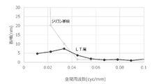
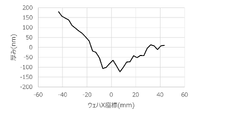
- FIG. 4C It is a figure which shows the shape of the silicon substrate of an Example. It is a figure which shows the film thickness distribution of the LT layer of an Example. It is a figure which shows the shape of the silicon substrate of an Example, and the FFT analysis result of the film thickness distribution of LT layer.
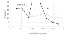
- FIG. 5C is a diagram showing enlarged vertical and horizontal axes of FIG. 5C. It is a figure which shows the shape of the silicon substrate of a comparative example. It is a figure which shows the film thickness distribution of the LT layer of a comparative example.
- FIG. 5 is a diagram showing FFT analysis results of the shape of a silicon substrate and the film thickness distribution of an LT layer in a comparative example; It is a figure which expands and shows the vertical axis
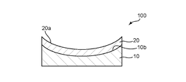
- FIG. 1 is a schematic cross-sectional view showing a schematic configuration of a composite substrate according to one embodiment of the present invention.
- the composite substrate 100 has a support substrate 10 and a piezoelectric layer 20 arranged on one side of the support substrate 10 .
- the composite substrate 100 may further have arbitrary layers. The type/function, number, combination, arrangement, etc. of such layers can be appropriately determined according to the purpose.
- composite substrate 100 may have an intermediate layer (eg, inorganic material layer) disposed between piezoelectric layer 20 and support substrate 10 .
- the composite substrate 100 may have a bonding layer arranged between the piezoelectric layer 20 or an intermediate layer (not shown) and the support substrate 10 .
- the composite substrate 100 can be manufactured in any suitable shape. In one embodiment, as shown in FIG. 2, it can be manufactured in so-called wafer form.
- the size of the composite substrate 100 can be appropriately set according to the purpose. For example, the wafer diameter is between 50 mm and 150 mm.
- the thickness of the supporting substrate 10 is, for example, 100 ⁇ m to 1000 ⁇ m.
- the supporting substrate has an amplitude of undulations exceeding a spatial frequency of 0.045 cyc/mm in the shape of 0 nm or more and 10 nm or less, preferably 5 nm or less.
- the support substrate may be composed of a single crystal, or may be composed of a polycrystal. Materials constituting the support substrate are preferably selected from the group consisting of silicon, sapphire, glass, quartz, crystal and alumina.
- the above silicon may be monocrystalline silicon, polycrystalline silicon, or high resistance silicon.
- the sapphire is a single crystal with a composition of Al 2 O 3 and the alumina is a polycrystal with a composition of Al 2 O 3 .
- the thermal expansion coefficient of the material forming the support substrate is preferably smaller than the thermal expansion coefficient of the material forming the piezoelectric layer, which will be described later.
- Such a support substrate can suppress changes in the shape and size of the piezoelectric layer when temperature changes, and can suppress, for example, changes in the frequency characteristics of the obtained surface acoustic wave device.
- A-2. Piezoelectric Layer Any suitable piezoelectric material can be used as a material constituting the piezoelectric layer.
- a single crystal with the composition LiAO 3 is preferably used as the piezoelectric material.
- A is one or more elements selected from the group consisting of niobium and tantalum.
- LiAO 3 may be lithium niobate (LiNbO 3 ), lithium tantalate (LiTaO 3 ), or a lithium niobate-lithium tantalate solid solution.
- the piezoelectric layer is arranged such that the normal direction is 32° to 55° (for example, 42° ) It is preferable to use a rotated direction, or (180°, 58° to 35°, 180°) in Euler angles, because the propagation loss is small.
- the piezoelectric layer has a normal direction rotated 37.8° from the Z axis to the ⁇ Y axis around the X axis, which is the propagation direction of surface acoustic waves. It is preferable to use the direction of (0°, 37.8°, 0°) in Euler angles because the electromechanical coupling coefficient is large. Further, for example, when the piezoelectric material substrate is lithium niobate, the normal direction of the piezoelectric layer is rotated from the Y axis to the Z axis by 40° to 65° around the X axis, which is the propagation direction of the surface acoustic wave. It is preferable to use the one in the direction of 180.degree., 50.degree.-25.degree.
- the thickness of the piezoelectric layer is preferably 5 ⁇ m or less, more preferably 3 ⁇ m or less, and even more preferably 1 ⁇ m or less.
- the thickness of the piezoelectric layer is, for example, 0.2 ⁇ m or more. With such a thickness, a high-performance surface acoustic wave device can be obtained. Specifically, it is expected that the temperature characteristics (TCF) can be improved, the Q value can be improved, and the like.
- the thickness of the piezoelectric layer is preferably uniform.
- 3A and 3B are diagrams showing an example outline of the shape of the support substrate (eg, in the X-axis direction) and the shape of the piezoelectric layer, respectively.
- the shape of the piezoelectric layer 20 can easily correspond to the undulation of the support substrate 10, and the piezoelectric layer 20 can be excellent in film thickness accuracy.
- the absolute value of the difference between the thickness (first thickness) T1 of the piezoelectric layer 20 at the first point and the thickness (second thickness) T2 of the piezoelectric layer at the second point is 100 nm or less. It is preferably 50 nm or less, more preferably 50 nm or less.
- a high-performance surface acoustic wave device can be obtained. Specifically, effects such as an improvement in the Q value are expected. Also, it is possible to obtain a surface acoustic wave device with small variations in characteristics. As shown in FIG.
- the thickness accuracy of the piezoelectric layer 20 can be excellent by satisfying the amplitude of the undulation of the support substrate.
- the composite substrate can have an intermediate layer.
- Materials forming the intermediate layer include, for example, silicon oxide, hafnium oxide, tantalum oxide, zirconium oxide, and aluminum oxide.
- the thickness of the intermediate layer is, for example, 0.1 ⁇ m to 2 ⁇ m.
- the intermediate layer can be deposited by any appropriate method.
- it can be deposited by sputtering, physical vapor deposition such as ion beam assisted deposition (IAD), chemical vapor deposition, or atomic layer deposition (ALD).
- IAD ion beam assisted deposition
- ALD atomic layer deposition
- the composite substrate may have a bonding layer.
- materials forming the bonding layer include silicon oxide, silicon, tantalum oxide, niobium oxide, aluminum oxide, titanium oxide, and hafnium oxide.
- the thickness of the bonding layer is, for example, 0.005 ⁇ m to 1 ⁇ m.
- the bonding layer can be deposited by any appropriate method. Specifically, it can be formed by a method similar to the method for forming the intermediate layer.
- Manufacturing Method A method for manufacturing a composite substrate according to one embodiment of the present invention includes bonding a support substrate to a first main surface side of a piezoelectric substrate having a first main surface and a second main surface facing each other, and Polishing the surface of the piezoelectric substrate on the side of the second main surface. Typically, polishing is performed after bonding.
- 4A to 4D are diagrams showing an example of a manufacturing process for a composite substrate according to one embodiment.
- FIG. 4A shows a state in which the polishing of both opposing main surfaces of the support substrate 10 has been completed.
- the lower surface 10a of the support substrate 10 is polished flat, and the upper surface 10b has a downwardly curved curved shape.
- the amplitude of the waviness of the shape of the support substrate 10 exceeding the spatial frequency of 0.045 cyc/mm is 0 nm or more and 10 nm or less, preferably 5 nm or less. Such values can be well achieved, for example, with the geometry of the illustrated example.
- the upper surface 10b may have an upwardly convex curved shape.
- FIG. 4B shows a state in which the support substrate 10 and the piezoelectric substrate 22 are directly bonded.
- the piezoelectric substrate 22 has a first main surface 22a and a second main surface 22b facing each other, and is bonded to the support substrate 10 after polishing the first main surface 22a.
- the bonding surfaces are preferably activated by any appropriate activation treatment.
- the activated surface of the support substrate 10 and the activated surface of the piezoelectric substrate 22 are brought into contact and pressed. Join directly with Thus, a joined body 90 shown in FIG. 4B is obtained.
- the second main surface 22b of the piezoelectric substrate 22 of the obtained joined body 90 is subjected to processing such as grinding and polishing so as to form a piezoelectric layer having the desired thickness.
- FIG. 4C shows the state in which the grinding of the second principal surface 22b is completed
- FIG. 4D shows the state in which the polishing of the second principal surface 22b is completed.
- the piezoelectric layer 20 is formed by polishing to obtain the composite substrate 100 .
- the shape of the upper surface 20a of the piezoelectric layer 20 can correspond to the shape of the upper surface 10b of the support substrate 10, for example.
- polishing method examples include chemical mechanical polishing (CMP), mirror polishing by lap polishing, and the like.
- CMP chemical mechanical polishing
- a chemical-mechanical polishing process is employed.
- a chemical mechanical polishing process using a polishing pad using a polishing slurry eg, colloidal silica is employed.
- abrasive residue for example, abrasive residue, process-affected layer, and the like.
- cleaning methods include wet cleaning, dry cleaning, and scrub cleaning.
- scrub cleaning is preferred because it allows simple and efficient cleaning.
- a cleaning agent for example, Sun Wash series manufactured by Lion Corporation
- a solvent for example, a mixed solution of acetone and isopropyl alcohol (IPA)
- IPA isopropyl alcohol
- the activation treatment is typically performed by irradiating a neutralizing beam.
- an apparatus such as the apparatus described in JP-A-2014-086400 is used to generate a neutralizing beam, and the activation treatment is performed by irradiating this beam.
- a saddle field fast atom beam source is used as the beam source, an inert gas such as argon or nitrogen is introduced into the chamber, and a high voltage is applied to the electrodes from a DC power source. Electrons are moved by a saddle field type electric field generated between the electrode (positive electrode) and the housing (negative electrode), and a beam of atoms and ions is generated by the inert gas.
- the ion beam is neutralized by the grid, so that a beam of neutral atoms is emitted from the fast atom beam source.
- the voltage during activation by beam irradiation is preferably 0.5 kV to 2.0 kV, and the current during activation by beam irradiation is preferably 50 mA to 200 mA.
- the contact and pressurization of the joint surfaces are preferably performed in a vacuum atmosphere.
- the temperature at this time is typically room temperature. Specifically, the temperature is preferably 20° C. or higher and 40° C. or lower, more preferably 25° C. or higher and 30° C. or lower.
- the applied pressure is preferably 100N to 20000N.
- a surface acoustic wave device has the above composite substrate.
- a surface acoustic wave device typically includes the composite substrate and electrodes (comb-shaped electrodes) provided on the piezoelectric layer side of the composite substrate.
- Such a surface acoustic wave device is suitably used as a SAW filter for communication equipment such as mobile phones.
- a lithium tantalate (LT) substrate with a diameter of 4 inches and a thickness of 500 ⁇ m (a 42° Y-cut X-propagation LT substrate, in which the direction of surface acoustic wave (SAW) propagation is X and the cutting angle is a rotated Y-cut plate) was prepared. .
- a silicon substrate having a diameter of 4 inches and a thickness of 500 ⁇ m was prepared, and the surface (both sides) of this silicon substrate was polished.
- a silicon substrate was placed on a SUS carrier of a CMP polishing machine, and a hard urethane pad was used, and colloidal silica was used as a polishing agent to perform double-sided polishing.
- both substrates were placed in a vacuum chamber and evacuated to a level of 10 ⁇ 6 Pa, and then a fast atom beam (accelerating voltage 1 kV, Ar flow rate 27 sccm) was applied for 80 seconds. After the irradiation, the beam-irradiated surfaces of both substrates were overlapped, and a pressure of 1200 kgf was applied for 2 minutes to bond the substrates to obtain a bonded body.
- a fast atom beam accelerating voltage 1 kV, Ar flow rate 27 sccm
- the back surface of the LT substrate of the bonded body was ground by a grinder from the initial 500 ⁇ m to 3 ⁇ m. Further, the substrate was mirror-polished with a CMP polishing machine using a hard urethane pad and colloidal silica as a polishing agent until the thickness became 1 ⁇ m, to obtain a composite substrate having a silicon substrate and an LT layer.
- a composite substrate was obtained in the same manner as in Example except that a non-woven fabric was used instead of the hard urethane pad when polishing both sides of the silicon substrate.
- FIGS. 5A, 5B and 6A, 6B show values obtained by subtracting the average value of the thickness.
- FFT Fast Fourier Transform
- the obtained absolute value was divided by 16 (32 data points/2) and then doubled in consideration of the influence of Hanning window processing. If the silicon substrate is convex downward (on the side where the LT substrate is not placed), unnecessary frequency components are generated when the Hanning window is multiplied. was calculated by inverting the data by subtracting from the maximum value.
- FIGS. 5C and 5D The results of the example are shown in FIGS. 5C and 5D, and the results of the comparative example are shown in FIGS. 6C and 6D.
- a composite substrate according to an embodiment of the present invention can typically be suitably used for a surface acoustic wave device.
Landscapes
- Physics & Mathematics (AREA)
- Acoustics & Sound (AREA)
- Engineering & Computer Science (AREA)
- Chemical & Material Sciences (AREA)
- Manufacturing & Machinery (AREA)
- Crystallography & Structural Chemistry (AREA)
- Materials Engineering (AREA)
- Metallurgy (AREA)
- Organic Chemistry (AREA)
- Surface Acoustic Wave Elements And Circuit Networks Thereof (AREA)
- Crystals, And After-Treatments Of Crystals (AREA)
Priority Applications (4)
| Application Number | Priority Date | Filing Date | Title |
|---|---|---|---|
| KR1020227024425A KR102810044B1 (ko) | 2021-06-11 | 2022-02-18 | 복합 기판 및 복합 기판의 제조 방법 |
| CN202280002596.1A CN115707351B (zh) | 2021-06-11 | 2022-02-18 | 复合基板及复合基板的制造方法 |
| EP22751240.7A EP4124679A4 (en) | 2021-06-11 | 2022-02-18 | COMPOSITE SUBSTRATE AND METHOD FOR MANUFACTURING COMPOSITE SUBSTRATE |
| US17/818,040 US20220399872A1 (en) | 2021-06-11 | 2022-08-08 | Composite substrate and method of producing composite substrate |
Applications Claiming Priority (2)
| Application Number | Priority Date | Filing Date | Title |
|---|---|---|---|
| JP2021097962A JP7075529B1 (ja) | 2021-06-11 | 2021-06-11 | 複合基板および複合基板の製造方法 |
| JP2021-097962 | 2021-06-11 |
Related Child Applications (1)
| Application Number | Title | Priority Date | Filing Date |
|---|---|---|---|
| US17/818,040 Continuation US20220399872A1 (en) | 2021-06-11 | 2022-08-08 | Composite substrate and method of producing composite substrate |
Publications (1)
| Publication Number | Publication Date |
|---|---|
| WO2022259627A1 true WO2022259627A1 (ja) | 2022-12-15 |
Family
ID=81746672
Family Applications (1)
| Application Number | Title | Priority Date | Filing Date |
|---|---|---|---|
| PCT/JP2022/006547 Ceased WO2022259627A1 (ja) | 2021-06-11 | 2022-02-18 | 複合基板および複合基板の製造方法 |
Country Status (2)
| Country | Link |
|---|---|
| JP (3) | JP7075529B1 (https=) |
| WO (1) | WO2022259627A1 (https=) |
Families Citing this family (2)
| Publication number | Priority date | Publication date | Assignee | Title |
|---|---|---|---|---|
| KR102916188B1 (ko) * | 2022-01-17 | 2026-01-21 | 엔지케이 인슐레이터 엘티디 | 복합 기판의 제조 방법 |
| WO2025263278A1 (ja) * | 2024-06-21 | 2025-12-26 | 京セラ株式会社 | 弾性波装置、通信装置、圧電基板、および圧電基板の製造方法 |
Citations (6)
| Publication number | Priority date | Publication date | Assignee | Title |
|---|---|---|---|---|
| JPH0992895A (ja) * | 1995-07-19 | 1997-04-04 | Matsushita Electric Ind Co Ltd | 圧電素子とその製造方法 |
| JP2001085648A (ja) * | 1999-07-15 | 2001-03-30 | Shin Etsu Handotai Co Ltd | 貼り合わせウエーハの製造方法および貼り合わせウエーハ |
| JP2004214505A (ja) * | 2003-01-07 | 2004-07-29 | Sumitomo Heavy Ind Ltd | 表面形状の測定方法、表面形状の測定プログラム及び記録媒体 |
| JP2014086400A (ja) | 2012-10-26 | 2014-05-12 | Mitsubishi Heavy Ind Ltd | 高速原子ビーム源およびそれを用いた常温接合装置 |
| WO2016158965A1 (ja) * | 2015-03-30 | 2016-10-06 | 京セラ株式会社 | 素子製造方法 |
| WO2019244471A1 (ja) * | 2018-06-22 | 2019-12-26 | 日本碍子株式会社 | 接合体および弾性波素子 |
Family Cites Families (8)
| Publication number | Priority date | Publication date | Assignee | Title |
|---|---|---|---|---|
| JPH08148957A (ja) * | 1994-11-18 | 1996-06-07 | Sumitomo Electric Ind Ltd | 圧電薄膜ウェハーおよびその製造法 |
| JPH08274285A (ja) * | 1995-03-29 | 1996-10-18 | Komatsu Electron Metals Co Ltd | Soi基板及びその製造方法 |
| JP5871282B2 (ja) | 2013-03-27 | 2016-03-01 | 信越化学工業株式会社 | 圧電性酸化物単結晶ウェーハの製造方法。 |
| DE112016000125B4 (de) | 2015-09-15 | 2020-06-25 | Ngk Insulators, Ltd. | Verbundwerkstoff-Substrat und Dicken-Tendenz-Schätzverfahren für ein piezoelektrisches Substrat |
| JP2019029941A (ja) * | 2017-08-02 | 2019-02-21 | 株式会社ディスコ | 弾性波デバイス用基板の製造方法 |
| KR102229746B1 (ko) | 2018-03-20 | 2021-03-18 | 엔지케이 인슐레이터 엘티디 | 압전성 재료 기판과 지지 기판의 접합체 |
| JP6698954B2 (ja) | 2018-05-17 | 2020-05-27 | 日本碍子株式会社 | 圧電性単結晶基板と支持基板との接合体 |
| WO2020250490A1 (ja) | 2019-06-11 | 2020-12-17 | 日本碍子株式会社 | 複合基板、弾性波素子および複合基板の製造方法 |
-
2021
- 2021-06-11 JP JP2021097962A patent/JP7075529B1/ja active Active
-
2022
- 2022-02-18 WO PCT/JP2022/006547 patent/WO2022259627A1/ja not_active Ceased
- 2022-05-12 JP JP2022078984A patent/JP7640493B2/ja active Active
-
2025
- 2025-02-19 JP JP2025024840A patent/JP7804803B2/ja active Active
Patent Citations (6)
| Publication number | Priority date | Publication date | Assignee | Title |
|---|---|---|---|---|
| JPH0992895A (ja) * | 1995-07-19 | 1997-04-04 | Matsushita Electric Ind Co Ltd | 圧電素子とその製造方法 |
| JP2001085648A (ja) * | 1999-07-15 | 2001-03-30 | Shin Etsu Handotai Co Ltd | 貼り合わせウエーハの製造方法および貼り合わせウエーハ |
| JP2004214505A (ja) * | 2003-01-07 | 2004-07-29 | Sumitomo Heavy Ind Ltd | 表面形状の測定方法、表面形状の測定プログラム及び記録媒体 |
| JP2014086400A (ja) | 2012-10-26 | 2014-05-12 | Mitsubishi Heavy Ind Ltd | 高速原子ビーム源およびそれを用いた常温接合装置 |
| WO2016158965A1 (ja) * | 2015-03-30 | 2016-10-06 | 京セラ株式会社 | 素子製造方法 |
| WO2019244471A1 (ja) * | 2018-06-22 | 2019-12-26 | 日本碍子株式会社 | 接合体および弾性波素子 |
Also Published As
| Publication number | Publication date |
|---|---|
| JP7075529B1 (ja) | 2022-05-25 |
| JP7804803B2 (ja) | 2026-01-22 |
| JP2025068047A (ja) | 2025-04-24 |
| TW202315313A (zh) | 2023-04-01 |
| JP7640493B2 (ja) | 2025-03-05 |
| JP2022189405A (ja) | 2022-12-22 |
| JP2022189738A (ja) | 2022-12-22 |
Similar Documents
| Publication | Publication Date | Title |
|---|---|---|
| JP6427714B2 (ja) | 接合体および弾性波素子 | |
| KR101972728B1 (ko) | 접합체 및 탄성파 소자 | |
| KR102428548B1 (ko) | 접합 방법 | |
| JP7804803B2 (ja) | 複合基板および複合基板の製造方法 | |
| TWI780103B (zh) | 彈性波元件及其製造方法 | |
| JPWO2015012005A1 (ja) | 複合基板及びその製法 | |
| CN111066243A (zh) | 弹性波元件及其制造方法 | |
| KR20210006995A (ko) | 접합체 및 탄성파 소자 | |
| CN113906674B (zh) | 复合基板、弹性波元件及复合基板的制造方法 | |
| KR102249061B1 (ko) | 접합체 및 탄성파 소자 | |
| JPWO2018203430A1 (ja) | 弾性波素子およびその製造方法 | |
| CN115707351B (zh) | 复合基板及复合基板的制造方法 | |
| JP6612002B1 (ja) | 接合体および弾性波素子 | |
| TWI914512B (zh) | 複合基板及複合基板的製造方法 | |
| WO2024004333A1 (ja) | 複合基板および複合基板の製造方法 | |
| EP4047819B1 (en) | Composite substrate for acoustic wave device | |
| CN113939998B (zh) | 复合基板、弹性波元件及复合基板的制造方法 | |
| WO2023135844A1 (ja) | 複合基板の製造方法 | |
| KR102961427B1 (ko) | 복합 기판 및 복합 기판의 제조 방법 | |
| KR20250160194A (ko) | 접합체의 제조 방법 |
Legal Events
| Date | Code | Title | Description |
|---|---|---|---|
| ENP | Entry into the national phase |
Ref document number: 2022751240 Country of ref document: EP Effective date: 20220825 |
|
| NENP | Non-entry into the national phase |
Ref country code: DE |