WO2022255414A1 - 接着テープ及び接着テープ巻回リール - Google Patents
接着テープ及び接着テープ巻回リール Download PDFInfo
- Publication number
- WO2022255414A1 WO2022255414A1 PCT/JP2022/022365 JP2022022365W WO2022255414A1 WO 2022255414 A1 WO2022255414 A1 WO 2022255414A1 JP 2022022365 W JP2022022365 W JP 2022022365W WO 2022255414 A1 WO2022255414 A1 WO 2022255414A1
- Authority
- WO
- WIPO (PCT)
- Prior art keywords
- adhesive tape
- adhesive layer
- adhesive
- end mark
- thickness
- Prior art date
- Legal status (The legal status is an assumption and is not a legal conclusion. Google has not performed a legal analysis and makes no representation as to the accuracy of the status listed.)
- Ceased
Links
Images



Classifications
-
- C—CHEMISTRY; METALLURGY
- C09—DYES; PAINTS; POLISHES; NATURAL RESINS; ADHESIVES; COMPOSITIONS NOT OTHERWISE PROVIDED FOR; APPLICATIONS OF MATERIALS NOT OTHERWISE PROVIDED FOR
- C09J—ADHESIVES; NON-MECHANICAL ASPECTS OF ADHESIVE PROCESSES IN GENERAL; ADHESIVE PROCESSES NOT PROVIDED FOR ELSEWHERE; USE OF MATERIALS AS ADHESIVES
- C09J201/00—Adhesives based on unspecified macromolecular compounds
-
- C—CHEMISTRY; METALLURGY
- C09—DYES; PAINTS; POLISHES; NATURAL RESINS; ADHESIVES; COMPOSITIONS NOT OTHERWISE PROVIDED FOR; APPLICATIONS OF MATERIALS NOT OTHERWISE PROVIDED FOR
- C09J—ADHESIVES; NON-MECHANICAL ASPECTS OF ADHESIVE PROCESSES IN GENERAL; ADHESIVE PROCESSES NOT PROVIDED FOR ELSEWHERE; USE OF MATERIALS AS ADHESIVES
- C09J7/00—Adhesives in the form of films or foils
- C09J7/30—Adhesives in the form of films or foils characterised by the adhesive composition
- C09J7/38—Pressure-sensitive adhesives [PSA]
-
- C—CHEMISTRY; METALLURGY
- C09—DYES; PAINTS; POLISHES; NATURAL RESINS; ADHESIVES; COMPOSITIONS NOT OTHERWISE PROVIDED FOR; APPLICATIONS OF MATERIALS NOT OTHERWISE PROVIDED FOR
- C09J—ADHESIVES; NON-MECHANICAL ASPECTS OF ADHESIVE PROCESSES IN GENERAL; ADHESIVE PROCESSES NOT PROVIDED FOR ELSEWHERE; USE OF MATERIALS AS ADHESIVES
- C09J9/00—Adhesives characterised by their physical nature or the effects produced, e.g. glue sticks
- C09J9/02—Electrically-conducting adhesives
-
- H—ELECTRICITY
- H01—ELECTRIC ELEMENTS
- H01B—CABLES; CONDUCTORS; INSULATORS; SELECTION OF MATERIALS FOR THEIR CONDUCTIVE, INSULATING OR DIELECTRIC PROPERTIES
- H01B1/00—Conductors or conductive bodies characterised by the conductive materials; Selection of materials as conductors
- H01B1/20—Conductive material dispersed in non-conductive organic material
- H01B1/22—Conductive material dispersed in non-conductive organic material the conductive material comprising metals or alloys
-
- C—CHEMISTRY; METALLURGY
- C09—DYES; PAINTS; POLISHES; NATURAL RESINS; ADHESIVES; COMPOSITIONS NOT OTHERWISE PROVIDED FOR; APPLICATIONS OF MATERIALS NOT OTHERWISE PROVIDED FOR
- C09J—ADHESIVES; NON-MECHANICAL ASPECTS OF ADHESIVE PROCESSES IN GENERAL; ADHESIVE PROCESSES NOT PROVIDED FOR ELSEWHERE; USE OF MATERIALS AS ADHESIVES
- C09J2301/00—Additional features of adhesives in the form of films or foils
- C09J2301/10—Additional features of adhesives in the form of films or foils characterized by the structural features of the adhesive tape or sheet
-
- C—CHEMISTRY; METALLURGY
- C09—DYES; PAINTS; POLISHES; NATURAL RESINS; ADHESIVES; COMPOSITIONS NOT OTHERWISE PROVIDED FOR; APPLICATIONS OF MATERIALS NOT OTHERWISE PROVIDED FOR
- C09J—ADHESIVES; NON-MECHANICAL ASPECTS OF ADHESIVE PROCESSES IN GENERAL; ADHESIVE PROCESSES NOT PROVIDED FOR ELSEWHERE; USE OF MATERIALS AS ADHESIVES
- C09J2301/00—Additional features of adhesives in the form of films or foils
- C09J2301/20—Additional features of adhesives in the form of films or foils characterized by the structural features of the adhesive itself
-
- C—CHEMISTRY; METALLURGY
- C09—DYES; PAINTS; POLISHES; NATURAL RESINS; ADHESIVES; COMPOSITIONS NOT OTHERWISE PROVIDED FOR; APPLICATIONS OF MATERIALS NOT OTHERWISE PROVIDED FOR
- C09J—ADHESIVES; NON-MECHANICAL ASPECTS OF ADHESIVE PROCESSES IN GENERAL; ADHESIVE PROCESSES NOT PROVIDED FOR ELSEWHERE; USE OF MATERIALS AS ADHESIVES
- C09J2301/00—Additional features of adhesives in the form of films or foils
- C09J2301/20—Additional features of adhesives in the form of films or foils characterized by the structural features of the adhesive itself
- C09J2301/208—Additional features of adhesives in the form of films or foils characterized by the structural features of the adhesive itself the adhesive layer being constituted by at least two or more adjacent or superposed adhesive layers, e.g. multilayer adhesive
Definitions
- the present disclosure relates to adhesive tapes and adhesive tape winding reels.
- Adhesive tapes such as anisotropic conductive tapes, for example, are used as connection materials for electrically connecting circuit members having a large number of electrodes to manufacture circuit connectors.
- Anisotropic conductive tape maintains conduction between opposing electrodes when connecting members such as semiconductor elements such as ICs and LSIs and packages to substrates such as printed wiring boards, glass substrates for LCDs, and flexible printed substrates. It is a connection material that performs electrical connection and mechanical fixation so as to maintain insulation between electrodes.
- an adhesive layer containing, for example, an adhesive component containing a thermosetting resin or the like and conductive particles is provided on one side of a substrate such as a PET film.
- the raw material of the tape is cut into a tape shape so that it has a width suitable for the application, and this is wound around a core to form an adhesive tape winding reel (for example, patent Reference 1).
- blocking is one of the causes of lowering the connection reliability between circuit members using adhesive tape. Blocking occurs when the adhesive layer in the wound body of the adhesive tape seeps out of the adhesive component to the outside of the base material (the side surface of the wound body of the adhesive tape wound on the reel), and the side plate of the reel and other parts of the adhesive tape are blocked. It is a phenomenon that it adheres to the part of When the adhesive tape is pulled out from the reel while blocking occurs, there is a problem that part of the adhesive layer is transferred to the back of the base material, or the adhesive layer peels off from the base material and only the base material is pulled out. may occur.
- the present disclosure has been made to solve the above problems, and aims to provide an adhesive tape and an adhesive tape winding reel that can effectively suppress the occurrence of blocking.
- the applicant of the present application has found that in the process of diligently working to suppress blocking that occurs in the wound body of the adhesive tape, the frequency of occurrence of blocking tends to increase when the remaining amount of the adhesive tape wound on the reel decreases. I found out. While searching for an improvement measure, we focused on the end mark given to the end portion of the adhesive tape.
- the end mark is a mark that indicates that the remaining amount of adhesive tape on the reel has run out.
- Conventional adhesive tapes are constructed, for example, by attaching an adhesive tape piece colored in a color different from that of the adhesive tape to the adhesive layer.
- a step due to the end mark may occur in the vicinity of the end mark-applied portion. For this reason, it is considered that stress is likely to be concentrated on the adhesive tape due to the step. Therefore, the applicant of the present application has obtained the knowledge that if the level difference due to the end mark can be alleviated and the concentration of stress on the adhesive tape due to the level difference can be alleviated, the occurrence of blocking can be effectively suppressed. I have completed the contents of
- An adhesive tape according to one aspect of the present disclosure is a long adhesive tape provided with an adhesive layer on one side of a base material, and the end portion of the adhesive tape is not provided with an adhesive layer and is attached to the base material. An exposed area where one side is exposed is provided, and in the exposed area, an adhesive tape piece as an end mark is provided on one side of the substrate.
- an exposed area where one side of the base material is exposed without providing an adhesive layer is provided at the end portion, and an adhesive tape piece is provided as an end mark in the exposed area.
- the thickness of the end mark may be equal to the thickness of the adhesive layer. In this case, there is no step between the adhesive layer and the end mark, and the step in the vicinity of the portion where the end mark is given in the wound body can be moderated. Therefore, it is possible to more effectively suppress the occurrence of blocking.
- the absolute value of the difference in thickness between the end mark and the adhesive layer may be less than the thickness of the adhesive layer.
- the step between the adhesive layer and the end mark and the step between the end mark and the base material can be reduced in a well-balanced manner, and the step in the vicinity of the portion where the end mark is given in the wound body can be preferably reduced. can be mitigated.
- the end mark may be spaced apart from the adhesive layer in the longitudinal direction of the adhesive tape.
- the gap between the adhesive layer and the end mark can function as an escape for the adhesive component that tends to seep out under stress. Therefore, it is possible to more effectively suppress the occurrence of blocking.
- the distance between the end marks with respect to the adhesive layer is less than the length of the end marks in the longitudinal direction. In this case, since the adhesive layer and the end mark are close to each other, the gap between the adhesive layer and the end mark functions as an escape allowance for the adhesive component, and the effect of reducing the step between the adhesive layer and the end mark is good. can be maintained at
- the exposed region may extend to the terminal edge of the adhesive tape with a length of at least one round of the winding core around which the adhesive tape is wound.
- An adhesive layer may be provided on one side of the base material in the area closer to the terminal edge of the adhesive tape than the end mark. In this case, since the end mark is sandwiched between the adhesive layers in the longitudinal direction of the adhesive tape, it is possible to more reliably reduce the step in the vicinity of the end mark-applied portion of the wound body.
- the width of the end mark may be smaller than the width of the base material. In this case, it is possible to form an escape margin for the adhesive component that tends to seep out under stress in the width direction of the adhesive tape. Therefore, it is possible to more effectively suppress the occurrence of blocking.
- the adhesive layer has a first adhesive layer and a second adhesive layer in order from the substrate side, and the first adhesive layer is composed of a cured product of a first curable composition containing conductive particles,
- the second adhesive layer may be composed of an uncured material of the second curable composition.
- the first adhesive which is a cured product of the first curable composition containing conductive particles containing conductive particles on the substrate side
- a configuration of the adhesive tape is useful in which layers are arranged and the second adhesive layer, which is an uncured product of the second curable composition, is arranged on the outer layer side.
- An adhesive tape winding reel is formed by winding the above adhesive tape around a winding core.
- an exposed region where one surface side of the base material is exposed without an adhesive layer is provided at the end portion, and the end portion is provided with an adhesive as an end mark.
- a piece of tape is provided.
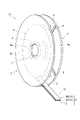
- FIG. 1 is a perspective view of an adhesive tape winding reel according to an embodiment of the present disclosure
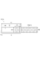
- FIG. FIG. 4 is a plan view showing the configuration of the terminal end portion of the adhesive tape according to the present embodiment
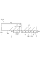
- 4 is a cross-sectional view taken along line III-III in FIG. 3
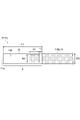
- FIG. FIG. 10 is a cross-sectional view showing the configuration of the terminal end portion of the adhesive tape according to the modification
- FIG. 11 is a plan view showing the configuration of the terminal portion of the adhesive tape according to another modification
- FIG. 11 is a plan view showing the configuration of the terminal portion of the adhesive tape according to still another modification
- FIG. 5 is a diagram showing results of an effect confirmation test of the present disclosure
- the numerical range indicated using “to” includes the numerical values before and after “to” as the minimum and maximum values, respectively.
- the upper limit value or lower limit value of the numerical range at one step may be replaced with the upper limit value or lower limit value of the numerical range at another step.
- the upper and lower limits of the numerical ranges may be replaced with the values shown in Examples. The upper and lower limits individually described can be combined arbitrarily.
- FIG. 1 is a perspective view showing an adhesive tape winding reel according to one embodiment of the present disclosure.
- the adhesive tape winding reel 1 includes a cylindrical core 2 and a pair of circular side plates 3, 3 provided at both ends of the core 2 in the axial direction.
- a long adhesive tape 11 is wound around the core 2 to form a wound body R.
- the outer diameter of the winding core 2 is, for example, approximately 50 mm to 160 mm.
- the side plate 3 has a sufficiently large diameter with respect to the winding core 2, for example.
- the side plate 3 has an inner surface 3a and an outer surface 3b.
- the interval between the side plates 3, 3 separated by the winding core 2 is appropriately set according to the width of the adhesive tape 11.
- the thickness of the side plate 3 is, for example, 0.5 mm to 5.0 mm, preferably 0.9 mm to 3.0 mm, more preferably 1.0 mm to 2.0 mm.
- the diameter of the side plate 3 is appropriately set according to the length of the adhesive tape 11 wound around the core 2 (the diameter of the wound body R of the adhesive tape 11).
- the winding core 2 and the pair of side plates 3, 3 may be integrally molded by injection molding or the like, or may be molded separately.
- the manufacturing process can be simplified.
- the dimension of the side plate 3 is changed according to the length of the adhesive tape 11 wound around the core 2, or the width of the adhesive tape 11 is changed. It becomes easy to change the dimension of 2.
- a central portion of the side plate 3 is provided with a shaft hole 4 into which a rotating shaft of a device in which the adhesive tape winding reel 1 is set when the adhesive tape 11 is used is inserted.
- the shaft hole 4 is provided with a notch portion 4a that fits into a convex portion provided on the rotating shaft side. The adhesive tape winding reel 1 can be prevented from idle by fitting the notch 4a into the projection.
- the inner surface 3a of the side plate 3 is provided with a plurality of ribs 5 extending radially between the center side and the edge side of the side plate 3. As shown in FIG. In the example of FIG. 1, four ribs 5 are provided around the center of the side plate 3 with a phase angle of 90°. The ribs 5 reduce the area of the side surface portion of the wound body R of the adhesive tape that contacts the inner surface 3 a of the side plate 3 . The ribs 5 contribute to suppressing the occurrence of blocking in the adhesive tape 11 together with the structure of the end marks 21 to be described later. Four or more ribs 5 may be provided, and may not necessarily be provided. [Structure of Adhesive Tape]
- an anisotropic conductive tape P is exemplified as the adhesive tape 11 .
- the anisotropic conductive tape P is a connecting material used for connecting members to be connected such as semiconductor elements such as ICs and LSIs and packages to substrates such as printed wiring boards, LCD glass substrates and flexible printed boards.
- the anisotropic conductive tape P is composed of a substrate 12 and an adhesive layer 13 provided on one surface 12a of the substrate 12 (see FIGS. 2 and 3).
- the adhesive layer 13 includes a first adhesive layer 13A and a second adhesive layer 13B.
- Layer 13B is laminated.
- the anisotropic conductive tape P is wound around the winding core 2 so that the adhesive layer 13 side faces inward. Therefore, in the state of the wound body R, the second adhesive layer 13B on the outer layer side is in contact with the base material 12 on the inner side by one turn.
- the first adhesive layer 13A is composed of a cured product of a first curable composition containing conductive particles 14 (see FIG. 3).
- the second adhesive layer 13B is composed of an uncured material of the second curable composition.
- an adhesive layer which is an uncured product of a curable composition
- an adhesive layer which is a cured product of a curable composition containing conductive particles
- the anisotropic conductive tape P according to this embodiment is a so-called inverted two-layer product.
- the first adhesive layer 13A which is a cured product of the first curable composition containing conductive particles 14, is provided on the substrate 12 side, and the uncured product of the second curable composition is provided on the substrate 12 side. is provided on the outer layer side. Since the second adhesive layer 13B is uncured, the second adhesive layer 13B can flow when the electrodes are connected.
- the length of the anisotropic conductive tape P is, for example, 1 m to 1000 m.
- the length of the anisotropic conductive tape P may be 50m to 500m, 100m to 500m, or 200m to 500m.
- the width of the anisotropic conductive tape P is, for example, 0.5 mm to 30 mm.
- the width of the anisotropic conductive tape P may be 0.5 mm to 2.0 mm, or may be 0.5 mm to 1.5 mm.
- Materials constituting the base material 12 include, for example, polyethylene terephthalate, polyethylene naphthalate, polyethylene isophthalate, polybutylene terephthalate, polyolefin, polyacetate, polycarbonate, polyphenylene sulfide, polyamide, ethylene-vinyl acetate copolymer, polyvinyl chloride, polyvinyl Examples include vinylidene chloride, synthetic rubber, and liquid crystal polymer.
- the base material 12 is separated from the first adhesive layer 13A when the anisotropic conductive tape P is used. Therefore, it is preferable that both surfaces (at least one surface 12a) of the substrate 12 are subjected to release treatment, plasma treatment, or the like.
- the width of the base material 12 is preferably equal to or wider than the first adhesive layer 13A and the second adhesive layer 13B formed thereon.
- the widths of the first adhesive layer 13A and the second adhesive layer 13B are appropriately set according to the intended use of the anisotropic conductive tape P.
- the thickness of the base material 12 is, for example, 4 ⁇ m to 200 ⁇ m.
- the thickness of substrate 12 may be between 20 ⁇ m and 100 ⁇ m.
- the first curable composition forming the first adhesive layer 13A is, for example, a photocurable composition and a thermosetting composition.
- This photo- and thermosetting composition contains (A) a polymerizable compound, (B) a photopolymerization initiator, and (C) a thermal polymerization initiator.
- the first adhesive layer 13A is formed, for example, by irradiating the first curable composition with light energy, polymerizing the component (A), and photocuring the light and thermosetting composition.
- the adhesive component of the first adhesive layer 13A includes at least the polymer of component (A) and component (C).
- the adhesive component may contain unreacted components (A) and (B).
- the first adhesive layer 13A may contain, as other components, a thermoplastic resin, a coupling agent, a filler, and the like.
- the conductive particles 14 contained in the first adhesive layer 13A are dispersed in the cured product of the first curable composition.
- the constituent material of the conductive particles 14 include metals such as Au, Ag, Ni, Cu, and solder.
- the conductive particles 14 may be made of conductive carbon.
- the conductive particles 14 may be obtained by coating a core made of conductive glass, ceramic, plastic, or the like with the metal or conductive carbon.
- the maximum particle size of the conductive particles 14 is smaller than the shortest distance between the symmetrically connected electrodes.
- the maximum particle size of the conductive particles 14 is, for example, 1.0 ⁇ m to 50 ⁇ m from the viewpoint of the dispersibility of the conductive particles 14 and the conductivity of the first adhesive layer 13A.
- the maximum particle size of the conductive particles 14 may be 2.0 ⁇ m to 30 ⁇ m. It may be from 2.5 ⁇ m to 20 ⁇ m.
- the average particle size of the conductive particles 14 is, for example, 1.0 ⁇ m to 10.0 ⁇ m from the viewpoint of the coating accuracy of the first adhesive layer 13A onto the substrate 12 and the dispersibility of the conductive particles 14 .
- the average particle size of the conductive particles 14 may be 2.0 ⁇ m to 8.5 ⁇ m, or may be 2.5 ⁇ m to 7.0 ⁇ m.
- a scanning electron microscope for example, can be used to measure the particle size of the conductive particles 14 .
- the particle size is measured by observation using a scanning electron microscope, the largest value among the measurement results is the maximum particle size, and the average value of the measurement results is the average particle size. can do.
- the conductive particles 14 have a non-spherical shape (for example, a shape having projections)
- the diameter of the circumscribed circle of the conductive particles on the image of the scanning electron microscope can be taken as the particle size of the conductive particles 14.
- the thickness of the first adhesive layer 13A is determined, for example, from the viewpoint of the ease of trapping the conductive particles 14 between the electrodes and the feasibility of reducing the connection resistance due to the conductive particles 14 being crushed and biting into the electrodes. It is 0.1 to 1.0 times the average particle size.
- the thickness of the first adhesive layer 13A may be 0.2 to 0.8 times or 0.3 to 0.7 times the average particle size of the conductive particles 14 . Part or all of the conductive particles 14 may protrude from the first adhesive layer 13A toward the second adhesive layer 13B.
- a scanning electron microscope for example, can be used to measure the thickness of the first adhesive layer 13A.
- the second curable composition forming the second adhesive layer 13B is, for example, a thermosetting composition.
- the thermosetting composition contains (a) a polymerizable compound and (b) a thermal polymerization initiator.
- the thermosetting composition may contain a thermosetting resin in place of or in addition to components (a) and (b). In this case, the thermosetting composition may contain a curing agent used for curing the thermosetting resin.
- the second adhesive layer 13B may contain a thermoplastic resin, a coupling agent, a filler, a softening agent, an accelerator, a deterioration inhibitor, a coloring agent, a flame retardant, a thixotropic agent, and the like.
- the thickness of the second adhesive layer 13B is appropriately set according to, for example, the height of the symmetrically connected electrodes.
- the thickness of the second adhesive layer 13B is, for example, 5 ⁇ m to 200 ⁇ m from the viewpoint of sealing between adjacent electrodes.
- the thickness ratio of the first adhesive layer 13A to the second adhesive layer 13B is, for example, 1 to 100 from the viewpoint of sealing between adjacent electrodes.
- the combined thickness of the first adhesive layer 13A and the second adhesive layer 13B is, for example, 5 ⁇ m to 200 ⁇ m.
- a scanning electron microscope for example, can be used to measure the thickness of the second adhesive layer 13B, similarly to the measurement of the thickness of the first adhesive layer 13A.
- FIG. 2 is a plan view showing the configuration of the end portion of the adhesive tape according to this embodiment.
- FIG. 3 is a sectional view taken along line III-III in FIG.
- the end portion of the anisotropic conductive tape P described above is provided with an exposed region K where the one surface 12a side of the substrate 12 is exposed without the adhesive layer 13 provided.
- the exposed region K extends to the terminal edge 11a of the anisotropic conductive tape P with a length of at least one turn of the winding core 2 around which the anisotropic conductive tape P is wound.
- the length L1 of the exposed area K is appropriately set, for example, based on the specifications of the device in which the adhesive tape winding reel 1 is set when the adhesive tape 11 is used, the specifications of the slitting equipment when manufacturing the reel, and the like.
- the length L1 of the exposed area K is, for example, 1 m to 50 m.
- the length of the exposed area K may be between 2 m and 20 m, or between 3 m and 10 m.
- an adhesive tape piece 22 as an end mark 21 is provided on the one surface 12a side of the base material 12 .
- the end mark 21 is a mark provided at the end portion of the anisotropic conductive tape P for automating the unwinding of the anisotropic conductive tape P from the adhesive tape winding reel 1 .
- the end mark 21 has a different color than the adhesive layer 13, for example. By detecting the end mark 21 with a sensor or the like, it is possible to inform the apparatus side or the operator side of the shortage of the remaining amount of the anisotropic conductive tape P on the adhesive tape winding reel 1 .
- Different colors here mean colors that can be distinguished from each other based on the three attributes of hue, saturation, and lightness, and may include metallic colors and fluorescent colors.
- the adhesive tape piece 22 forming the end mark 21 is, for example, a tape piece having an adhesive layer on one side of a base material.
- the constituent material of the base include acrylic resin and polyethylene terephthalate.
- adhesives constituting the adhesive layer include acrylic adhesives, silicone adhesives, rubber adhesives, and the like.
- the ratio of the thickness of the adhesive layer in the adhesive tape piece 22 to the thickness of the adhesive layer 13 prevents the adhesive from seeping out when the adhesive tape 11 is wound around the winding core 2 and prevents end marks from the adhesive layer 13. From the viewpoint of simultaneously preventing peeling of No. 21, it is, for example, 1:1 to 20:1.
- the ratio may be from 1:1 to 10:1, or from 2:1 to 5:1.
- the end mark 21 has a rectangular shape in plan view, as shown in FIG.
- the length L2 of the end mark 21 in the longitudinal direction of the anisotropic conductive tape P is not particularly limited, but is set to, for example, 5 cm or more from the viewpoint of ensuring ease of detection by a sensor.
- the length L2 of the end mark 21 may be 1 m or less.
- a portion after the end mark 21 is a portion that cannot be used as the adhesive tape 11 . Therefore, by reducing the length L2 of the end mark 21, the amount of discarded portions can be reduced.
- the width W1 of the end mark 21 is the same width as the width W2 of the substrate 12 . That is, in the example of FIG. 2, the edge in the width direction of the base material 12 and the edge in the width direction of the end mark 21 are aligned.
- the end mark 21 is located near the adhesive layer 13 in the exposed region K and is spaced apart from the adhesive layer 13 adjacent to the exposed region K in the longitudinal direction of the anisotropic conductive tape P. That is, between the adhesive layer 13 and the end mark 21, the one surface 12a of the substrate 12 is exposed with a separation width T1.
- a separation width T1 of the end mark 21 with respect to the adhesive layer 13 is, for example, equal to or less than the length L1 of the end mark 21 .
- the separation width T1 is, for example, 0.1 mm to 50 mm.
- the separation width T1 may be, for example, 0.5 mm to 20 mm, or may be 1 mm to 10 mm.
- the thickness D1 of the end mark 21 is equal to the thickness D2 of the adhesive layer 13 .
- the thickness of the adhesive layer 13 here is the sum of the thickness of the first adhesive layer 13A and the thickness of the second adhesive layer 13B. Equal thickness may include thickness differences due to manufacturing tolerances of the adhesive layer 13 and the end marks 21 . Since the thickness D1 of the end mark 21 is equal to the thickness D2 of the adhesive layer 13, substantially no step is generated between the adhesive layer 13 and the end mark 21.
- the exposed region K in which the one surface 12a side of the base material 12 is exposed without being provided with the adhesive layer 13 is provided at the end portion.
- a strip 22 is provided.
- the thickness D1 of the end mark 21 and the thickness D2 of the adhesive layer 13 are the same. Therefore, there is no step between the adhesive layer 13 and the end mark 21, and the step in the vicinity of the portion of the wound body R to which the end mark 21 is applied can be moderated. Therefore, it is possible to more effectively suppress the occurrence of blocking.
- the end marks 21 are arranged apart from the adhesive layer 13 in the longitudinal direction of the adhesive tape 11 . According to such a configuration, the gap between the adhesive layer 13 and the end mark 21 can function as an escape margin for the adhesive components that tend to seep out under stress. Therefore, it is possible to more effectively suppress the occurrence of blocking.
- the distance T1 between the end marks 21 and the adhesive layer 13 is less than or equal to the length of the end marks 21 in the longitudinal direction.
- the gap between the adhesive layer 13 and the end mark 21 functions as an escape allowance for the adhesive component, while the gap between the adhesive layer 13 and the end mark 21 can maintain the step reduction effect of For example, in a state in which the adhesive tape 11 is wound around the winding core 2, stress can be prevented from concentrating on the edge of the adhesive layer 13 adjacent to the exposed region K, and the occurrence of blocking at that portion can be effectively suppressed. It becomes possible.
- the exposed area K extends to the terminal edge 11a of the adhesive tape 11 with a length of at least one turn of the winding core around which the adhesive tape 11 is wound.
- the adhesive layer 13 has a first adhesive layer 13A and a second adhesive layer 13B in order from the substrate 12 side.
- the first adhesive layer 13A is composed of a cured material of the first curable composition containing the conductive particles 14, and the second adhesive layer 13B is composed of an uncured material of the second curable composition. It is
- the first adhesive which is a cured product of the first curable composition containing conductive particles containing conductive particles on the substrate side
- a configuration of the adhesive tape is useful in which layers are arranged and the second adhesive layer, which is an uncured product of the second curable composition, is arranged on the outer layer side.
- the thickness D1 of the end mark 21 and the thickness D2 of the adhesive layer 13 are equal, but the difference between the thickness D1 of the end mark 21 and the thickness D2 of the adhesive layer 13 is The absolute value may be less than the thickness D2 of the adhesive layer 13 . In this case, the difference in level between the adhesive layer 13 and the end mark 21 and the difference in level between the end mark 21 and the base material 12 can be reduced in a well-balanced manner. Nearby steps can be moderated favorably.
- the thickness D1 of the end mark 21 is about half the thickness D2 of the adhesive layer 13. There may be.
- the ratio of the thickness D1 of the end mark 21 to the thickness D2 of the adhesive layer 13 is not particularly limited, but is, for example, 1:1 to 20:1. The ratio may be from 1:1 to 10:1, or from 2:1 to 5:1.
- the width W1 of the end mark 21 is equal to the width W2 of the substrate 12, but as shown in FIG. It may be.
- the width of the adhesive tape 11 can also be formed to provide an escape margin for the adhesive component that tends to seep out under stress. Therefore, it is possible to more effectively suppress the occurrence of blocking.
- a ratio of the width W1 of the end mark 21 to the width W2 of the base material 12 is not particularly limited, but is, for example, 1:1 to 3:1. The ratio may be from 1:1 to 2:1, or from 1:1 to 5:4.
- the exposed region K extends to the terminal edge 11a of the adhesive tape 11, but as shown in FIG.
- An adhesive layer 13 may be provided on the one surface 12a side of 12 .
- An exposed region K is formed between the adhesive layers 13, 13 on which the end marks 21 are arranged. In this case, the end mark 21 is sandwiched between the adhesive layers 13 , 13 in the longitudinal direction of the adhesive tape 11 . Therefore, it is possible to more reliably reduce the step in the vicinity of the end-marked portion of the wound body R.
- the end mark 21 and the adhesive layer 13 on the terminal edge 11a side are separated in the longitudinal direction of the adhesive tape 11 .
- a spacing width T2 between the end mark 21 and the adhesive layer 13 on the side of the trailing edge 11a is equal to a spacing width T1 between the end mark 21 and the adhesive layer 13 on the front stage side. These spacing widths T1 and T2 may be different from each other.
- a varnish of a photocurable composition and a thermosetting composition was applied onto a PET film with a thickness of 50 ⁇ m using a coating device. Then, hot air drying was performed at 70° C. for 3 minutes to form a layer composed of a photocurable composition and a thermosetting composition having a thickness (thickness after drying) of 4 ⁇ m on the PET film. The thickness here was measured using a contact thickness gauge.
- the layer composed of the photocurable composition and the thermosetting composition was irradiated with light using a metal halide lamp so that the cumulative amount of light was 1500 mJ/cm 2 to polymerize the polymerizable compound.
- the photocurable and thermosetting composition was cured to obtain a first film in which a first adhesive layer was formed on the PET film.
- the density of the conductive particles at this time was approximately 7000 pcs/mm 2 . If the thickness of the first adhesive layer is less than the thickness (diameter) of the conductive particles, measuring the thickness of the layer using a contact thickness gauge will reflect the thickness of the conductive particles, indicating the presence of the conductive particles. Area thickness can be measured. For this reason, after producing a two-layer adhesive tape in which the first adhesive layer and the second adhesive layer are laminated, the first adhesive layer located in the spaced part between the adjacent conductive particles is subjected to the above-described method. Thickness was measured.
- the varnish of the thermosetting composition was applied on a PET film with a thickness of 50 ⁇ m using a coating device. Then, hot air drying was performed at 70° C. for 3 minutes to form a second adhesive layer having a thickness of 8 ⁇ m on the PET film. As a result, a second film having a second adhesive layer formed on the PET film was obtained. After that, the first film and the second film were laminated with a roll laminator while being heated at 40°C. At this time, the PET film on the second film side was peeled off to prepare an adhesive film in which the first adhesive layer and the second adhesive layer were laminated in this order on the PET film.
- the obtained adhesive film was cut to a width of 1.0 mm by roll-to-roll slitting equipment to produce an adhesive tape according to Example 1.
- the adhesive tape was wound around an adhesive tape winding reel so that the adhesive layer faced the core side (inside) and the base material faced the outside to obtain a wound body.
- Two lengths of adhesive tape were used, 50 m and 200 m.
- the adhesive layer was removed from the terminal edge of the adhesive tape to a position of 5 m to form an exposed area where one side of the substrate was exposed. In this exposed area, a piece of black adhesive tape was applied as an end mark at a distance of 1 mm from the adhesive layer.
- the total thickness of the first adhesive layer and the second adhesive layer was 12 ⁇ m, while the thickness of the end mark was 12 ⁇ m.
- Example 2 the configuration was the same as in Example 1 except that the end mark was attached at a distance of 10 mm from the adhesive layer.
- Example 3 the configuration was the same as that in Example 1 except that the thickness of the end mark was set to 30 ⁇ m.
- Example 4 the configuration was the same as in Example 2 except that the end mark was attached at a distance of 10 mm from the adhesive layer.
- Comparative Example 1 the same end mark as in Example 1 was attached on the adhesive layer at a position 5 m from the terminal edge of the adhesive tape without forming an exposed region.
- Comparative Example 2 had the same configuration as Comparative Example 2 except that the thickness of the end mark was 30 ⁇ m. (Evaluation of connection resistance)
- a COF (manufactured by FLEXSEED) with a pitch of 25 ⁇ m and a glass substrate with a thin film electrode (manufactured by Geomatec) having a thin film electrode (height: 1200 ⁇ ) made of amorphous indium tin oxide (ITO) on a glass substrate are attached to each adhesive tape.
- the apparatus was used to apply heat and pressure to a width of 1 mm under the conditions of 170° C., 6 MPa, and 4 seconds to fabricate a circuit connection structure.
- a sample of each adhesive tape was attached to the COF substrate from the second adhesive layer side, and after peeling off the base material, it was placed facing the glass substrate and heated and pressurized.
- connection resistance value between the counter electrodes immediately after connection and after the high temperature and high humidity test was measured with a multimeter.
- each circuit connection structure was left in a thermo-hygrostat at 85° C. and 85% RH for 240 hours.
- the connection resistance value was the average value of 16 points of resistance between the opposing electrodes.
- FIG. 7 is a diagram showing the results of the effect confirmation test of the present disclosure. As shown in the figure, in all of Examples 1 to 4 and Comparative Examples 1 and 2, the connection resistance was 1.5 ⁇ , and the connection resistance after the high temperature and high humidity test was 2.2 ⁇ . Therefore, in any of Examples 1 to 4, it was confirmed that a connection state equivalent to that of Comparative Examples 1 and 2, which are conventional configurations in which an end mark was provided on the adhesive layer, could be realized.
Landscapes
- Chemical & Material Sciences (AREA)
- Organic Chemistry (AREA)
- Physics & Mathematics (AREA)
- Dispersion Chemistry (AREA)
- Spectroscopy & Molecular Physics (AREA)
- Adhesive Tapes (AREA)
- Storage Of Web-Like Or Filamentary Materials (AREA)
Priority Applications (3)
| Application Number | Priority Date | Filing Date | Title |
|---|---|---|---|
| CN202280033542.1A CN117280008A (zh) | 2021-06-02 | 2022-06-01 | 黏合带及黏合带卷绕卷轴 |
| JP2023525894A JPWO2022255414A1 (https=) | 2021-06-02 | 2022-06-01 | |
| KR1020237038249A KR20240015631A (ko) | 2021-06-02 | 2022-06-01 | 접착 테이프 및 접착 테이프 권회 릴 |
Applications Claiming Priority (2)
| Application Number | Priority Date | Filing Date | Title |
|---|---|---|---|
| JP2021-092808 | 2021-06-02 | ||
| JP2021092808 | 2021-06-02 |
Publications (1)
| Publication Number | Publication Date |
|---|---|
| WO2022255414A1 true WO2022255414A1 (ja) | 2022-12-08 |
Family
ID=84324171
Family Applications (1)
| Application Number | Title | Priority Date | Filing Date |
|---|---|---|---|
| PCT/JP2022/022365 Ceased WO2022255414A1 (ja) | 2021-06-02 | 2022-06-01 | 接着テープ及び接着テープ巻回リール |
Country Status (4)
| Country | Link |
|---|---|
| JP (1) | JPWO2022255414A1 (https=) |
| KR (1) | KR20240015631A (https=) |
| CN (1) | CN117280008A (https=) |
| WO (1) | WO2022255414A1 (https=) |
Citations (3)
| Publication number | Priority date | Publication date | Assignee | Title |
|---|---|---|---|---|
| JP2001284005A (ja) * | 2000-03-28 | 2001-10-12 | Hitachi Chem Co Ltd | 異方導電材テープ |
| WO2012121292A1 (ja) * | 2011-03-09 | 2012-09-13 | 日立化成工業株式会社 | 回路接続用テープ、接着剤リール、積層テープの回路接続材料としての使用、積層テープの回路接続材料の製造のための使用及び回路接続体の製造方法 |
| WO2013024873A1 (ja) * | 2011-08-18 | 2013-02-21 | 日立化成工業株式会社 | 接着材リール、ブロッキング抑制方法、接着材リールの交換方法、接着材テープの繰出し方法、接着材リールの製造方法、リールキット、及び梱包体 |
Family Cites Families (1)
| Publication number | Priority date | Publication date | Assignee | Title |
|---|---|---|---|---|
| JP3959247B2 (ja) | 2001-02-16 | 2007-08-15 | ソニーケミカル&インフォメーションデバイス株式会社 | リール部材及びフィルムの巻取方法 |
-
2022
- 2022-06-01 JP JP2023525894A patent/JPWO2022255414A1/ja active Pending
- 2022-06-01 CN CN202280033542.1A patent/CN117280008A/zh active Pending
- 2022-06-01 KR KR1020237038249A patent/KR20240015631A/ko active Pending
- 2022-06-01 WO PCT/JP2022/022365 patent/WO2022255414A1/ja not_active Ceased
Patent Citations (3)
| Publication number | Priority date | Publication date | Assignee | Title |
|---|---|---|---|---|
| JP2001284005A (ja) * | 2000-03-28 | 2001-10-12 | Hitachi Chem Co Ltd | 異方導電材テープ |
| WO2012121292A1 (ja) * | 2011-03-09 | 2012-09-13 | 日立化成工業株式会社 | 回路接続用テープ、接着剤リール、積層テープの回路接続材料としての使用、積層テープの回路接続材料の製造のための使用及び回路接続体の製造方法 |
| WO2013024873A1 (ja) * | 2011-08-18 | 2013-02-21 | 日立化成工業株式会社 | 接着材リール、ブロッキング抑制方法、接着材リールの交換方法、接着材テープの繰出し方法、接着材リールの製造方法、リールキット、及び梱包体 |
Also Published As
| Publication number | Publication date |
|---|---|
| CN117280008A (zh) | 2023-12-22 |
| KR20240015631A (ko) | 2024-02-05 |
| JPWO2022255414A1 (https=) | 2022-12-08 |
Similar Documents
| Publication | Publication Date | Title |
|---|---|---|
| JP6489516B2 (ja) | 異方導電性フィルム | |
| CN105826418B (zh) | 连接结构的制造方法以及太阳能电池模块的制造方法 | |
| JP4596089B2 (ja) | 接着材リール | |
| WO2013024544A1 (ja) | 接着材リール | |
| WO2010098354A1 (ja) | 接着材リール | |
| US10513635B2 (en) | Anisotropic conductive film | |
| JP2014102943A (ja) | 異方性導電フィルム、接続方法、及び接合体 | |
| CN109804002B (zh) | 含填料膜 | |
| WO2022255414A1 (ja) | 接着テープ及び接着テープ巻回リール | |
| WO2025105288A1 (ja) | 回路接続用接着フィルムの巻回体の製造方法、及び回路接続用接着フィルムの巻回体 | |
| JP3035579B2 (ja) | 異方性導電接着フィルム | |
| JP2002358825A (ja) | 異方導電性接着フィルム | |
| JP3712334B2 (ja) | 異方導電性接着フィルム | |
| JP4872230B2 (ja) | 電磁波シールド付きフラットケーブル及びその製造方法、並びに電磁波シールド転写箔 | |
| WO2012121292A1 (ja) | 回路接続用テープ、接着剤リール、積層テープの回路接続材料としての使用、積層テープの回路接続材料の製造のための使用及び回路接続体の製造方法 | |
| TWI781213B (zh) | 異向性導電膜、連接結構體及彼等之製造方法 | |
| JP2562273B2 (ja) | 銅メッキファインピッチコネクタ部材の製造方法 | |
| CN219772026U (zh) | 一种透明导电胶带 | |
| CN101742826B (zh) | 嵌入式线路板的线路的修补方法 | |
| JP2005330409A (ja) | 接着フィルム、接着剤付き基板の製造方法、及び接着フィルムの製造方法 | |
| WO2024247856A1 (ja) | 粘着フィルムの製造方法、粘着フィルム、粘着フィルム半完成品、及び接続構造体の製造方法 | |
| JP2024171325A (ja) | 粘着フィルムの製造方法、粘着フィルム、粘着フィルム半完成品、及び接続構造体の製造方法 | |
| WO2023189767A1 (ja) | 個片加工接着フィルム、接続構造体の製造方法、及び接続構造体 | |
| WO2024195598A1 (ja) | フィラー含有フィルム | |
| TWI380084B (en) | Liquid crystal display panel and fabricating method thereof |
Legal Events
| Date | Code | Title | Description |
|---|---|---|---|
| 121 | Ep: the epo has been informed by wipo that ep was designated in this application |
Ref document number: 22816159 Country of ref document: EP Kind code of ref document: A1 |
|
| WWE | Wipo information: entry into national phase |
Ref document number: 2023525894 Country of ref document: JP |
|
| WWE | Wipo information: entry into national phase |
Ref document number: 202280033542.1 Country of ref document: CN |
|
| NENP | Non-entry into the national phase |
Ref country code: DE |
|
| 122 | Ep: pct application non-entry in european phase |
Ref document number: 22816159 Country of ref document: EP Kind code of ref document: A1 |