WO2022249336A1 - 電線および電線の製造方法 - Google Patents
電線および電線の製造方法 Download PDFInfo
- Publication number
- WO2022249336A1 WO2022249336A1 PCT/JP2021/020001 JP2021020001W WO2022249336A1 WO 2022249336 A1 WO2022249336 A1 WO 2022249336A1 JP 2021020001 W JP2021020001 W JP 2021020001W WO 2022249336 A1 WO2022249336 A1 WO 2022249336A1
- Authority
- WO
- WIPO (PCT)
- Prior art keywords
- electric wire
- wire
- copper layer
- outer peripheral
- peripheral surface
- Prior art date
- Legal status (The legal status is an assumption and is not a legal conclusion. Google has not performed a legal analysis and makes no representation as to the accuracy of the status listed.)
- Ceased
Links
Images






Classifications
-
- H—ELECTRICITY
- H01—ELECTRIC ELEMENTS
- H01B—CABLES; CONDUCTORS; INSULATORS; SELECTION OF MATERIALS FOR THEIR CONDUCTIVE, INSULATING OR DIELECTRIC PROPERTIES
- H01B5/00—Non-insulated conductors or conductive bodies characterised by their form
- H01B5/02—Single bars, rods, wires, or strips
Definitions
- the present disclosure relates to electric wires and methods of manufacturing electric wires.
- Patent Document 1 discloses a first sensor including a core made of stainless steel, a coating layer made of copper or a copper alloy, and a Ni layer disposed between the core and the coating layer.
- a stranded wire for a wire harness is disclosed, which includes strands of wire and a Ni layer having a thickness of 0.05 ⁇ m or more and 5 ⁇ m or less.
- a wire according to the present disclosure includes a wire containing iron as a main component, a nickel layer on the outer peripheral surface of the wire, and a copper layer on the outer peripheral surface of the nickel layer.
- the thickness of the nickel layer is 0.3 nm or more and 40.3 nm or less.
- a wire according to the present disclosure includes a wire containing iron as a main component and a copper layer on the outer peripheral surface of the wire.
- the arithmetic average roughness (Ra) of the outer peripheral surface of the copper layer is 0.1 ⁇ m or more and 3.4 ⁇ m or less.
- the electric wire according to the present disclosure is an electric wire including a wire containing iron as a main component and a copper layer on the outer peripheral surface of the wire.
- One end of the wire has an end face.
- the end face has a surface that is slanted with respect to an imaginary plane perpendicular to the longitudinal axis of the wire.
- a method for manufacturing an electric wire according to the present disclosure includes steps of preparing a wire containing iron as a main component, forming a nickel layer on the outer peripheral surface of the wire, and forming a copper layer on the outer peripheral surface of the nickel layer. and including.
- the step of forming the nickel layer includes forming the nickel layer so that the nickel layer has a thickness of 0.3 nm or more and 40.3 nm or less.
- a method for manufacturing an electric wire according to the present disclosure includes the steps of preparing a wire containing iron as a main component, forming a copper layer on the outer peripheral surface of the wire, and processing a part of the electric wire to form an end face on the electric wire. and forming.
- Forming the end face includes forming the end face such that the end face has a surface that is slanted with respect to an imaginary plane perpendicular to the longitudinal axis of the wire.
- a method for manufacturing an electric wire according to the present disclosure includes the steps of preparing a wire containing iron as a main component, forming a copper layer on the outer peripheral surface of the wire, and cutting a part of the electric wire to form an end face on the electric wire. and forming.
- the step of forming the end face includes a step of forming the end face so that the end face has a surface that is inclined with respect to a plane perpendicular to the longitudinal direction of the wire.
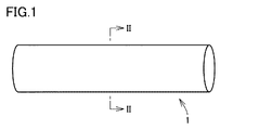
- FIG. 1 is a schematic perspective view of an electric wire 1 according to the first embodiment.
- FIG. 2 is a schematic cross-sectional view along II-II in FIG.
- FIG. 3 is a flow chart of the electric wire manufacturing method according to the first embodiment.
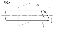
- FIG. 4 is a schematic perspective view of the electric wire according to the second embodiment.
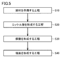
- FIG. 5 is a flow chart of the electric wire manufacturing method according to the second embodiment.
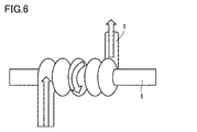
- FIG. 6 is a schematic perspective view illustrating the evaluation method of Evaluation 1-1.
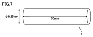
- FIG. 7 is a schematic perspective view of the wires of samples 1-1 to 1-6 cut in evaluation 1-2.
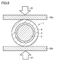
- FIG. 8 is a schematic cross-sectional view illustrating the evaluation method of Evaluation 1-2.
- FIG. 9 is a schematic cross-sectional view of an example of electric wires of samples 1-2 to 1-6 of evaluation criteria X of evaluation 1-2 and evaluation 1-3.
- FIG. 10 is a schematic cross-sectional view of an example of electric wires of samples 1-2 to 1-6 of evaluation criteria Y of evaluation 1-2 and evaluation 1-3.
- FIG. 11 is a schematic cross-sectional view of an example of electric wires of samples 1-2 to 1-6 of evaluation criteria Z of evaluation 1-2 and evaluation 1-3.
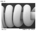
- FIG. 12 is an enlarged photograph of an example of electric wires of samples 2-1 to 2-5 of evaluation criteria X of evaluation 2-1 and evaluation 2-2.
- FIG. 13 is an enlarged photograph of an example of electric wires of samples 2-1 to 2-5 of evaluation criteria Y of evaluation 2-1 and evaluation 2-2.
- An object of the present disclosure is to provide an electric wire and an electric wire manufacturing method capable of suppressing cracks in a copper layer when external stress is applied to the electric wire.
- Another object of the present disclosure is to provide an electric wire and an electric wire manufacturing method capable of suppressing peeling of a copper layer when stress is applied to the electric wire from the outside.
- An object of the present disclosure is to provide an electric wire and an electric wire manufacturing method capable of suppressing peeling of a copper layer when stress is applied to the electric wire from the outside.
- the electric wire 1 includes a wire 2 containing iron as a main component, a nickel layer 3 on the outer peripheral surface of the wire 2, and a copper layer 4 on the outer peripheral surface of the nickel layer 3. .
- the thickness of the nickel layer 3 is 0.3 nm or more and 40.3 nm or less. This makes it possible to suppress the occurrence of cracks in the copper layer 4 when stress is applied to the wire 1 from the outside.
- the diameter of the wire 2 of the electric wire 1 according to (1) above is 0.2 mm or more and 0.3 mm or less. In this case as well, it is possible to suppress the occurrence of cracks in the copper layer 4 when stress is applied to the wire 1 from the outside.
- the thickness of the copper layer 4 of the electric wire 1 according to (1) or (2) above is 40 ⁇ m or more and 60 ⁇ m or less. In this case as well, it is possible to suppress the occurrence of cracks in the copper layer 4 when stress is applied to the wire 1 from the outside.
- the wire 2 of the electric wire 1 according to any one of (1) to (3) above contains stainless steel. In this case as well, it is possible to suppress the occurrence of cracks in the copper layer 4 when stress is applied to the wire 1 from the outside.
- the wire 2 of the electric wire 1 according to any one of (1) to (4) above contains carbon steel. In this case as well, it is possible to suppress the occurrence of cracks in the copper layer 4 when stress is applied to the wire 1 from the outside.
- the arithmetic average roughness (Ra) of the outer peripheral surface of the copper layer 4 of the electric wire 1 according to any one of (1) to (5) above is 0.1 ⁇ m or more and 3.4 ⁇ m or less. In this case, when stress is applied to the electric wire 1 from the outside, it is possible to suppress the occurrence of cracks in the copper layer 4 and to suppress the peeling of the copper layer 4 from the nickel layer 3. can.
- the thickness of the nickel layer 3 of the electric wire 1 according to any one of (1) to (6) above is 0.3 nm or more and 25.3 nm or less. In this case, there is a greater tendency to suppress the occurrence of cracks in the copper layer 4 when stress is applied to the wire 1 from the outside.
- the thickness of the nickel layer 3 of the electric wire 1 according to any one of (1) to (7) above is 0.3 nm or more and 9.8 nm or less. In this case, there is a greater tendency to suppress the occurrence of cracks in the copper layer 4 when stress is applied to the wire 1 from the outside.
- One end of the electric wire 1 according to any one of (1) to (8) above has an end surface 1a.
- the end surface 1a has a surface that is inclined with respect to a virtual surface 1c perpendicular to the longitudinal axis 1b of the electric wire 1. As shown in FIG. As a result, even when pressure is applied to the electric wire 1 from the outside, the end surface 1a of the electric wire 1 can disperse the pressure, so that peeling of the copper layer 4 from the nickel layer 3 can be suppressed.
- the electric wire 1 includes a wire 2 containing iron as a main component and a copper layer 4 on the outer peripheral surface of the wire 2 .
- the arithmetic average roughness (Ra) of the outer peripheral surface of the copper layer 4 is 0.1 ⁇ m or more and 3.4 ⁇ m or less.
- the electric wire 1 includes a wire 2 containing iron as a main component and a copper layer 4 on the outer peripheral surface of the wire 2 .
- One end of the electric wire 1 has an end surface 1a.
- the end surface 1a has a surface that is inclined with respect to a virtual surface 1c perpendicular to the longitudinal axis 1b of the electric wire 1. As shown in FIG. As a result, even when pressure is applied to the electric wire 1 from the outside, the end surface 1a of the electric wire 1 can disperse the pressure, so that peeling of the copper layer 4 can be suppressed.
- the method for manufacturing the electric wire 1 includes a step of preparing a wire 2 containing iron as a main component, a step of forming a nickel layer 3 on the outer peripheral surface of the wire 2, and an outer peripheral surface of the nickel layer 3. forming a copper layer 4 thereon.
- the step of forming nickel layer 3 includes a step of forming nickel layer 3 so that the thickness of nickel layer 3 is 0.3 nm or more and 40.3 nm or less. This makes it possible to suppress the occurrence of cracks in the copper layer 4 when stress is applied to the wire 1 from the outside.
- the method for manufacturing the electric wire 1 according to the present disclosure includes a step of preparing a wire 2 containing iron as a main component, a step of forming a copper layer 4 on the outer peripheral surface of the wire 2, and a part of the electric wire 1 forming the end surface 1a on the electric wire 1 by processing.
- the step of forming the end face 1a includes the step of forming the end face 1a so that the end face 1a has a surface inclined with respect to a virtual plane 1c orthogonal to the longitudinal axis 1b of the electric wire 1. FIG. Thereby, peeling of the copper layer 4 can be suppressed when stress is applied to the electric wire 1 from the outside.
- the method for manufacturing the electric wire 1 includes a step of preparing a wire 2 containing iron as a main component, a step of forming a copper layer 4 on the outer peripheral surface of the wire 2, and a part of the electric wire 1 and a step of forming an end face 1a on the electric wire 1 by cutting.
- the step of forming the end face 1a includes forming the end face 1a such that the end face 1a has a surface that is inclined with respect to an imaginary plane 1c perpendicular to the longitudinal axis 1b of the wire. Thereby, peeling of the copper layer 4 can be suppressed when stress is applied to the electric wire 1 from the outside.
- FIG. 1 is a schematic perspective view of an electric wire 1 according to the first embodiment.
- the electric wire 1 according to the first embodiment has a linear structure extending in one direction (longitudinal direction).
- FIG. 2 is a schematic cross-sectional view along II-II in FIG.
- the electric wire 1 according to the first embodiment includes a wire 2, a nickel layer 3 on the outer peripheral surface of the wire 2, and a copper layer on the outer peripheral surface of the nickel layer 3 from the inside of the electric wire 1. 4 and .
- the wire 2 contains iron as a main component.
- the term “main component” means the component having the largest number of atoms among the components constituting the wire or layer. Therefore, the component with the largest number of atoms among the components forming the wire 2 is iron.
- the wire 2 for example, a wire containing stainless steel (SUS) or carbon steel can be used.
- the vertical cross section of wire 2 orthogonal to the longitudinal direction of electric wire 1 may be circular, for example.
- diameter R of the vertical cross section of wire 2 may be, for example, 0.2 mm or more and 0.3 mm or less.
- the nickel layer 3 is a layer containing nickel as its main component. Therefore, nickel has the largest number of atoms among the components forming the nickel layer 3 .
- the thickness T1 of the nickel layer 3 is 0.3 nm or more and 40.3 nm or less.
- the thickness T1 of the nickel layer 3 can be measured, for example, with a transmission electron microscope "JEM-2100F" manufactured by JEOL Ltd.
- the thickness T1 of the nickel layer 3 may be, for example, 0.3 nm or more and 25.3 nm or less, or may be 0.3 nm or more and 9.8 nm or less.
- the thickness T1 of the nickel layer 3 is 0.3 nm or more and 25.3 nm or less, particularly when it is 0.3 nm or more and 9.8 nm or less, external stress is applied to the electric wire 1 and the nickel layer 3 and the copper layer are separated. Even if 4 is deformed, damage caused to the copper layer 4 by the deformed nickel layer 3 can be further reduced, so that cracks in the copper layer 4 can be further suppressed.
- the copper layer 4 is a layer containing copper as its main component. Therefore, the component with the largest number of atoms among the components forming the copper layer 4 is copper.
- a thickness T2 of the copper layer 4 may be, for example, 40 ⁇ m or more and 60 ⁇ m or less.
- the arithmetic mean roughness (Ra) of the outer peripheral surface of the copper layer 4 can be, for example, 0.1 ⁇ m or more and 3.4 ⁇ m or less.
- the arithmetic average roughness (Ra) of the outer peripheral surface of the copper layer 4 is larger than 3.4 ⁇ m, the outer peripheral surface of the copper layer 4 tends to be rough and a plurality of recesses are formed on the outer peripheral surface of the copper layer 4. It is in. In this case, when pressure is applied from the outside of the electric wire 1 , cracks are likely to occur in the copper layer 4 starting from recesses on the outer peripheral surface of the copper layer 4 .
- the arithmetic mean roughness (Ra) of the outer peripheral surface of the copper layer 4 is 0.1 ⁇ m or more and 3.4 ⁇ m or less, particularly when it is 0.1 ⁇ m or more and 1.1 ⁇ m or less, pressure is applied from the outside of the electric wire 1. It is possible to suppress cracks in the copper layer 4 and to suppress peeling of the copper layer 4 from the nickel layer 3 when the voltage is applied.
- arithmetic mean roughness (Ra) is a physical quantity defined in JIS B 0601 (1994) or JIS B 0031 (1994).
- “Arithmetic mean roughness (Ra)” can be measured by, for example, "VX-K100 series” manufactured by Keyence Corporation.
- FIG. 3 is a flowchart of the method for manufacturing the electric wire 1 according to the first embodiment.
- a method for manufacturing the electric wire 1 according to the first embodiment will be described with reference to FIG. 3 .
- step S10 of preparing the wire rod 2 is performed.
- the step S10 of preparing the wire 2 can be performed by preparing a wire such as SUS or carbon steel containing iron as a main component, for example.
- step S20 of forming nickel layer 3 is performed.
- Step S20 of forming nickel layer 3 can be performed, for example, by forming nickel layer 3 on the outer peripheral surface of wire rod 2 by electroplating using Wood's bath.
- the nickel layer 3 is formed such that the thickness T1 of the nickel layer 3 is 0.3 nm or more and 40.3 nm or less.
- the thickness T1 of the nickel layer 3 can be set to 0.3 nm or more and 40.3 nm or less by adjusting the current density and the electroplating time in electroplating using Wood's bath, for example.
- a step of degreasing the outer peripheral surface of the wire rod 2 and then washing it with water may be performed before the step S20 of forming the nickel layer 3.
- step S30 of forming copper layer 4 is performed.
- Step S30 of forming copper layer 4 can be performed by forming copper layer 4 on the outer peripheral surface of nickel layer 3 by, for example, electroplating using copper sulfate plating.
- a step of washing the outer peripheral surface of copper layer 4 with water may be performed after step S30 of forming copper layer 4 .
- the electric wire 1 according to the first embodiment can be manufactured.
- the thickness T1 of the nickel layer 3 of the electric wire 1 according to the first embodiment is 0.3 nm or more and 40.3 nm or less, 0.3 nm or more and 25.3 nm or less, or 0.3 nm or more and 9.8 nm or less. It is said that Therefore, in the electric wire 1 according to the first embodiment, it is possible to suppress the occurrence of cracks in the copper layer 4 when stress is applied to the electric wire 1 from the outside.
- the arithmetic mean roughness (Ra) of the outer peripheral surface of the copper layer 4 of the electric wire 1 according to the first embodiment is 0.1 ⁇ m or more and 3.4 ⁇ m or less, particularly 0.1 ⁇ m or more 1
- FIG. 4 is a schematic perspective view of the electric wire 1 according to the second embodiment.
- the electric wire 1 according to the second embodiment has an end surface 1a at one end of the electric wire 1, and the end surface 1a is inclined with respect to a virtual plane 1c perpendicular to the longitudinal axis 1b of the electric wire 1. It is characterized by having
- FIG. 5 is a flow chart of the method for manufacturing the electric wire 1 according to the second embodiment. As shown in FIG. 5, the method of manufacturing the electric wire 1 according to the second embodiment is characterized in that the step S40 of forming the end face 1a is performed after the step S30 of forming the copper layer 4. As shown in FIG. 5, the step S40 of forming the end face 1a is performed after the step S30 of forming the copper layer 4. As shown in FIG. 5, the step S40 of forming the end face 1a is performed after the step S30 of forming the copper layer 4. As shown in FIG.
- the step S40 of forming the end face 1a can be performed, for example, by processing and/or cutting a portion of the electric wire 1 to form the end face 1a.
- processing is a superordinate concept of “cutting”, and is a concept including “cutting” and work other than “cutting”.
- one end of the electric wire 1 has an end face 1a, and the end face 1a has a surface inclined with respect to a virtual plane 1c orthogonal to the longitudinal axis 1b of the electric wire 1.
- the end surface 1a of the electric wire 1 according to the second embodiment has a surface inclined with respect to the virtual plane 1c perpendicular to the longitudinal axis 1b of the electric wire 1, so that external pressure is applied to the electric wire 1. Even in such a case, the end surface 1a of the electric wire 1 can disperse the pressure, so that the separation of the copper layer 4 from the nickel layer 3 can be suppressed.
- samples 1-2 to 1-6 having the configurations shown in Table 2 were produced.
- Samples 1-2 to 1-6 were produced by the same method and under the same conditions except that the thickness of the nickel layer was changed by changing the electroplating time of the nickel layer in (3) the nickel layer forming step. rice field.
- the composition and pH of Wood's bath in Table 1 are as follows. Nickel chloride: 240 [g / L] Hydrochloric acid: 125 [mL/L] pH: 1.5 or less
- composition of the acid copper plating bath in Table 1 is as follows. Copper sulfate pentahydrate: 150 to 250 [g / L] Sulfuric acid: 30 to 100 [g/L] Chlorine ion: 5 to 80 [mg / L]
- Sample 1-1 was produced by the same method and under the same conditions as Samples 1-2 to 1-6, except that (3) the step of forming the nickel layer was not performed.
- a 150x SEM image of the outer peripheral surface of the copper layer of the electric wire 1 of the samples 1-1 to 1-6 after the application of the pressure is obtained, and the copper layer of the electric wire 1 of the samples 1-1 to 1-6. Evaluation of the outer peripheral surface of (evaluation 1-3) was performed according to the following evaluation criteria. Table 2 shows the results.
- FIG. 9 is a schematic cross-sectional view of an example of electric wire 1 of samples 1-2 to 1-6 of evaluation criteria X of evaluation 1-2 and evaluation 1-3.
- FIG. 10 is a schematic cross-sectional view of an example of electric wires 1 of samples 1-2 to 1-6 of evaluation criteria Y of evaluation 1-2 and evaluation 1-3.
- FIG. 11 is a schematic cross-sectional view of an example of electric wires 1 of samples 1-2 to 1-6 of evaluation criteria Z of evaluation 1-2 and evaluation 1-3. 10 and 11 show an example of cracks 31 generated in the copper layer 4.
- FIG. 10 show an example of cracks 31 generated in the copper layer 4.
- the thickness of the nickel layer is 0.3 nm.
- the wires 1 of Samples 1-1 and 1-6 which do not fall within the range of 40.3 nm or less, the occurrence of cracks in the copper layer is suppressed when stress is applied to the wire 1 from the outside. was confirmed to be possible.
- the thickness of the nickel layer is 0. .
- the copper layer is cracked when a stress is applied to the wire 1 from the outside. It was confirmed that it is possible to suppress the occurrence of
- the thickness of the nickel layer is 0. .
- the wires 1 of Samples 1-1 and Samples 1-4 to 1-6 which do not fall within the range of 3 nm or more and 9.8 nm or less, cracks occurred in the copper layer when stress was applied to the wire 1 from the outside. It was confirmed that it is possible to suppress the occurrence of
- the thickness of the nickel layer shown in Table 2 is a value measured with a transmission electron microscope "JEM-2100F" manufactured by JEOL Ltd.
- Sample 2-1 was prepared in the same manner and under the same conditions as the electric wire of Sample 1-2 except that the current density of copper electroplating in the step of forming the copper layer (4) was set to the conditions shown in Table 3 below.
- ⁇ 2-4 wires were made.
- the wire of sample 2-5 was prepared in the same manner and under the same conditions as the wire of sample 2-4, except that an additive was added to the electrolytic plating bath of copper sulfate.
- FIG. 12 is an enlarged photograph of an example of electric wires of samples 2-1 to 2-5 of evaluation criteria X of evaluation 2-1 and evaluation 2-2.
- FIG. 13 is an enlarged photograph of an example of electric wires of samples 2-1 to 2-5 of evaluation criteria Y of evaluation 2-1 and evaluation 2-2.
- the value of the arithmetic mean roughness Ra [ ⁇ m] in the column of "arithmetic mean roughness Ra [ ⁇ m]" in Table 3 is obtained by It is a value measured based on JIS B 0601 (1994) or JIS B 0031 (1994) using "VX-K100 series” manufactured by Keyence.
Landscapes
- Non-Insulated Conductors (AREA)
Abstract
電線は、主成分として鉄を含む線材と、線材の外周面上の銅層とを備えている。
Description
本開示は、電線および電線の製造方法に関する。
WO2018/092350号公報(特許文献1)には、ステンレス鋼からなる芯部と、銅または銅合金からなる被覆層と、芯部と被覆層との間に配置されるNi層とを含む第1素線を備え、Ni層の厚みが0.05μm以上5μm以下である、ワイヤーハーネス用撚り線が開示されている。
本開示に係る電線は、主成分として鉄を含む線材と、線材の外周面上のニッケル層と、ニッケル層の外周面上の銅層と、を備えている。ニッケル層の厚さは、0.3nm以上40.3nm以下である。
本開示に係る電線は、主成分として鉄を含む線材と、線材の外周面上の銅層と、を備えている。銅層の外周面の算術平均粗さ(Ra)は、0.1μm以上3.4μm以下である。
本開示に係る電線は、主成分として鉄を含む線材と、線材の外周面上の銅層と、を備える電線である。電線の一端が端面を有する。端面は、電線の長手方向軸に直交する仮想面に対して傾斜する面を有する。
本開示に係る電線の製造方法は、主成分として鉄を含む線材を準備する工程と、線材の外周面上にニッケル層を形成する工程と、ニッケル層の外周面上に銅層を形成する工程と、を含む。ニッケル層を形成する工程は、ニッケル層の厚さが0.3nm以上40.3nm以下となるようにニッケル層を形成する工程を含む。
本開示に係る電線の製造方法は、主成分として鉄を含む線材を準備する工程と、線材の外周面上に銅層を形成する工程と、電線の一部を加工することによって電線に端面を形成する工程と、を含む。端面を形成する工程は、端面が電線の長手方向軸に直交する仮想面に対して傾斜する面を有するように端面を形成する工程を含む。
本開示に係る電線の製造方法は、主成分として鉄を含む線材を準備する工程と、線材の外周面上に銅層を形成する工程と、電線の一部を切断することによって電線に端面を形成する工程とを含む。端面を形成する工程は、端面が電線の長手方向に直交する面に対して傾斜する面を有するように端面を形成する工程を含む。
[本開示が解決しようとする課題]
本開示の目的は、電線に外部から応力が印加されたときに銅層に割れが発生するのを抑制することが可能な電線および電線の製造方法を提供することにある。
本開示の目的は、電線に外部から応力が印加されたときに銅層に割れが発生するのを抑制することが可能な電線および電線の製造方法を提供することにある。
本開示の別の目的は、電線に外部から応力が印加されたときに銅層が剥離するのを抑制することが可能な電線および電線の製造方法を提供することにある。
[本開示の効果]
本開示によれば、電線に外部から応力が印加されたときに銅層に割れが発生するのを抑制することが可能な電線および電線の製造方法を提供することができる。
本開示によれば、電線に外部から応力が印加されたときに銅層に割れが発生するのを抑制することが可能な電線および電線の製造方法を提供することができる。
本開示によれば、電線に外部から応力が印加されたときに銅層が剥離するのを抑制することが可能な電線および電線の製造方法を提供することにある。
[本開示の実施形態の説明]
最初に本開示の実施形態を列挙して説明する。
最初に本開示の実施形態を列挙して説明する。
(1)本開示に係る電線1は、主成分として鉄を含む線材2と、線材2の外周面上のニッケル層3と、ニッケル層3の外周面上の銅層4と、を備えている。ニッケル層3の厚さは、0.3nm以上40.3nm以下である。これにより、電線1に外部から応力が印加されたときに銅層4に割れが発生するのを抑制することが可能となる。
(2)上記(1)に係る電線1の線材2の直径は、0.2mm以上0.3mm以下である。この場合にも、電線1に外部から応力が印加されたときに銅層4に割れが発生するのを抑制することが可能となる。
(3)上記(1)または上記(2)に係る電線1の銅層4の厚さは、40μm以上60μm以下である。この場合にも、電線1に外部から応力が印加されたときに銅層4に割れが発生するのを抑制することが可能となる。
(4)上記(1)から上記(3)のいずれかに係る電線1の線材2は、ステンレス鋼を含む。この場合にも、電線1に外部から応力が印加されたときに銅層4に割れが発生するのを抑制することが可能となる。
(5)上記(1)から上記(4)のいずれかに係る電線1の線材2は、炭素鋼を含む。この場合にも、電線1に外部から応力が印加されたときに銅層4に割れが発生するのを抑制することが可能となる。
(6)上記(1)から上記(5)のいずれかに係る電線1の銅層4の外周面の算術平均粗さ(Ra)は、0.1μm以上3.4μm以下である。この場合には、電線1に外部から応力が印加されたときに、銅層4に割れが発生するのを抑制することができるとともに、ニッケル層3から銅層4が剥離するのを抑制することできる。
(7)上記(1)から上記(6)のいずれかに係る電線1のニッケル層3の厚さは、0.3nm以上25.3nm以下である。この場合には、電線1に外部から応力が印加されたときに銅層4に割れが発生するのを抑制することができる傾向が大きくなる。
(8)上記(1)から上記(7)のいずれかに係る電線1のニッケル層3の厚さは、0.3nm以上9.8nm以下である。この場合には、電線1に外部から応力が印加されたときに銅層4に割れが発生するのを抑制することができる傾向がさらに大きくなる。
(9)上記(1)から上記(8)のいずれかに係る電線1の一端が端面1aを有している。端面1aは、電線1の長手方向軸1bに直交する仮想面1cに対して傾斜する面を有している。これにより、電線1に外部から圧力が印加された場合でも電線1の端面1aが圧力を分散することができるため、ニッケル層3から銅層4が剥離するのを抑制することできる。
(10)本開示に係る電線1は、主成分として鉄を含む線材2と、線材2の外周面上の銅層4と、を備えている。銅層4の外周面の算術平均粗さ(Ra)は、0.1μm以上3.4μm以下である。これにより、電線1に外部から圧力が印加された場合でも銅層4に割れが発生するのを抑制することができるとともに、電線1の端面1aが圧力を分散することができるため、ニッケル層3から銅層4が剥離するのを抑制することできる。
(11)本開示に係る電線1は、主成分として鉄を含む線材2と、線材2の外周面上の銅層4と、を備えている。電線1の一端が端面1aを有している。端面1aは、電線1の長手方向軸1bに直交する仮想面1cに対して傾斜する面を有する。これにより、電線1に外部から圧力が印加された場合でも電線1の端面1aが圧力を分散することができるため、銅層4が剥離するのを抑制することできる。
(12)本開示に係る電線1の製造方法は、主成分として鉄を含む線材2を準備する工程と、線材2の外周面上にニッケル層3を形成する工程と、ニッケル層3の外周面上に銅層4を形成する工程と、を含んでいる。ニッケル層3を形成する工程は、ニッケル層3の厚さが0.3nm以上40.3nm以下となるようにニッケル層3を形成する工程を含む。これにより、電線1に外部から応力が印加されたときに銅層4に割れが発生するのを抑制することが可能となる。
(13)本開示に係る電線1の製造方法は、主成分として鉄を含む線材2を準備する工程と、線材2の外周面上に銅層4を形成する工程と、電線1の一部を加工することによって電線1に端面1aを形成する工程とを含んでいる。端面1aを形成する工程は、端面1aが電線1の長手方向軸1bに直交する仮想面1cに対して傾斜する面を有するように端面1aを形成する工程を含んでいる。これにより、電線1に外部から応力が印加されたときに銅層4が剥離するのを抑制することできる。
(14)本開示に係る電線1の製造方法は、主成分として鉄を含む線材2を準備する工程と、線材2の外周面上に銅層4を形成する工程と、電線1の一部を切断することによって電線1に端面1aを形成する工程とを含んでいる。端面1aを形成する工程は、端面1aが電線の長手方向軸1bに直交する仮想面1cに対して傾斜する面を有するように端面1aを形成する工程を含んでいる。これにより、電線1に外部から応力が印加されたときに銅層4が剥離するのを抑制することできる。
[本開示の実施形態の詳細]
次に、図面に基づいて本開示の実施形態の詳細について説明する。なお、以下の図面において同一または相当する部分には同一の参照番号を付し、その説明は繰返さない。
次に、図面に基づいて本開示の実施形態の詳細について説明する。なお、以下の図面において同一または相当する部分には同一の参照番号を付し、その説明は繰返さない。
<第1実施形態>
まず、第1実施形態に係る電線1の構成について説明する。図1は、第1実施形態に係る電線1の模式的な斜視図である。図1に示されるように、第1実施形態に係る電線1は一方向(長手方向)に延在する線状構造を有している。
まず、第1実施形態に係る電線1の構成について説明する。図1は、第1実施形態に係る電線1の模式的な斜視図である。図1に示されるように、第1実施形態に係る電線1は一方向(長手方向)に延在する線状構造を有している。
図2は、図1のII-IIに沿った模式的な断面図である。図2に示されるように、第1実施形態に係る電線1は、電線1の内側から、線材2と、線材2の外周面上のニッケル層3と、ニッケル層3の外周面上の銅層4と、を備えている。
線材2は、主成分として鉄を含む。本明細書において、「主成分」とは、線材または層を構成する成分のうち、最も原子数の多い成分を意味する。したがって、線材2を構成する成分のうち最も原子数の多い成分は鉄である。線材2としては、たとえば、ステンレス鋼(SUS)または炭素鋼を含む線材を用いることができる。
図2に示されるように、電線1の長手方向に直交する線材2の縦断面(電線1の長手方向に直交する断面)は、たとえば、円形であってもよい。線材2の縦断面が円形である場合の線材2の縦断面の直径Rは、たとえば0.2mm以上0.3mm以下であり得る。
ニッケル層3は、ニッケルを主成分として含む層である。したがって、ニッケル層3を構成する成分のうち最も原子数の多い成分はニッケルである。
第1実施形態に係る電線1において、ニッケル層3の厚さT1は、0.3nm以上40.3nm以下とされる。ニッケル層3の厚さT1が0.3nm以上40.3nm以下である場合には、電線1に外部から応力が印加されたときに銅層4に割れが発生するのを抑制することができる。ニッケル層3の厚さT1は、たとえば、日本電子株式会社製の透過型電子顕微鏡「JEM-2100F」により測定することができる。
ニッケル層3の厚さT1は、たとえば、0.3nm以上25.3nm以下であってもよく、0.3nm以上9.8nm以下であってもよい。ニッケル層3の厚さT1が0.3nm以上25.3nm以下である場合、特に0.3nm以上9.8nm以下である場合には電線1に外部から応力が印加されてニッケル層3と銅層4とが変形したとしても、変形したニッケル層3が銅層4に与えるダメージをさらに低減することができるため、銅層4に割れが発生するのをさらに抑制することができる。
銅層4は、銅を主成分として含む層である。したがって、銅層4を構成する成分のうち最も原子数の多い成分は銅である。銅層4の厚さT2は、たとえば40μm以上60μm以下であり得る。
銅層4の外周面の算術平均粗さ(Ra)は、たとえば0.1μm以上3.4μm以下であり得る。銅層4の外周面の算術平均粗さ(Ra)が3.4μmよりも大きい場合には銅層4の外周面が粗くなって、銅層4の外周面に複数の凹部が形成される傾向にある。この場合に、電線1の外部から圧力が印加されると、銅層4の外周面の凹部が起点となって、銅層4に割れが生じやすくなる。銅層4の外周面の算術平均粗さ(Ra)が0.1μm以上3.4μm以下である場合、特に、0.1μm以上1.1μm以下である場合には、電線1の外部から圧力が印加されたときに、銅層4に割れが生じるのを抑制することができるとともに、ニッケル層3から銅層4が剥離するのを抑制することできる。
なお、本明細書において、「算術平均粗さ(Ra)」は、JIS B 0601(1994)またはJIS B 0031(1994)に定義される物理量である。「算術平均粗さ(Ra)」は、たとえば、株式会社キーエンス製の「VX-K100series」により測定することができる。
図3は、第1実施形態に係る電線1の製造方法のフローチャートである。以下、図3を参照して、第1実施形態に係る電線1の製造方法について説明する。
まず、図3に示されるように、線材2を準備する工程S10を行なう。線材2を準備する工程S10は、たとえば、主成分として鉄を含むSUSまたは炭素鋼等の線材を準備することにより行なうことができる。
次に、ニッケル層3を形成する工程S20を行なう。ニッケル層3を形成する工程S20は、たとえば、ウッド浴を用いた電解めっきにより、線材2の外周面上にニッケル層3を形成することにより行なうことができる。
ニッケル層3を形成する工程S20においては、ニッケル層3の厚さT1が0.3nm以上40.3nm以下となるようにニッケル層3が形成される。ニッケル層3の厚さT1は、たとえば、ウッド浴を用いた電解めっきにおける電流密度および電解めっき時間を調整することにより、0.3nm以上40.3nm以下とすることができる。なお、ニッケル層3を形成する工程S20の前に、線材2の外周面を脱脂した後に水洗する工程を行なってもよい。
次に、銅層4を形成する工程S30を行なう。銅層4を形成する工程S30は、たとえば、硫酸銅めっきを用いた電解めっきにより、ニッケル層3の外周面上に銅層4を形成することにより行なうことができる。なお、銅層4を形成する工程S30の後に、銅層4の外周面を水洗する工程を行なってもよい。
以上の工程を経ることにより、第1実施形態に係る電線1を製造することができる。
上述のように、第1実施形態に係る電線1のニッケル層3の厚さT1は、0.3nm以上40.3nm以下、0.3nm以上25.3nm以下、または0.3nm以上9.8nm以下とされている。したがって、第1実施形態に係る電線1においては、電線1に外部から応力が印加されたときに銅層4に割れが発生するのを抑制することができる。
また、上述のように、第1実施形態に係る電線1の銅層4の外周面の算術平均粗さ(Ra)が0.1μm以上3.4μm以下である場合、特に、0.1μm以上1.1μm以下である場合には、第1実施形態に係る電線1においては、銅層4に割れが発生するのを抑制することができるとともに、ニッケル層3から銅層4が剥離するのを抑制することできる。
<第2実施形態>
次に、第2実施形態に係る電線1の構成について説明する。図4は、第2実施形態に係る電線1の模式的な斜視図である。図4に示されるように、第2実施形態に係る電線1は電線1の一端が端面1aを有し、端面1aが電線1の長手方向軸1bに直交する仮想面1cに対して傾斜する面を有することを特徴としている。
次に、第2実施形態に係る電線1の構成について説明する。図4は、第2実施形態に係る電線1の模式的な斜視図である。図4に示されるように、第2実施形態に係る電線1は電線1の一端が端面1aを有し、端面1aが電線1の長手方向軸1bに直交する仮想面1cに対して傾斜する面を有することを特徴としている。
図5は、第2実施形態に係る電線1の製造方法のフローチャートである。図5に示されるように、第2実施形態に係る電線1の製造方法は、銅層4を形成する工程S30の後に端面1aを形成する工程S40を行なうことを特徴としている。
端面1aを形成する工程S40は、たとえば、電線1の一部を加工および/または切断することによって端面1aを形成することにより行なうことができる。なお、本明細書において、「加工」は「切断」の上位概念であり、「切断」と「切断」以外の作業とを含む概念である。
第2実施形態に係る電線1においては、電線1の一端が端面1aを有し、端面1aが電線1の長手方向軸1bに直交する仮想面1cに対して傾斜する面を有している。このように、第2実施形態に係る電線1の端面1aが電線1の長手方向軸1bに直交する仮想面1cに対して傾斜する面を有することによって、電線1に外部から圧力が印加された場合でも電線1の端面1aが圧力を分散することができるため、ニッケル層3から銅層4が剥離するのを抑制することできる。
第2実施形態における上記以外の説明は、第1実施形態における説明と同様であるためその説明については省略する。
<試料1-1~1-6の作製>
まず、SUS304または炭素鋼からなる線材の外周面について、以下の表1に示す条件で、(1)脱脂工程を行なった後に(2)水洗工程を行なった。
まず、SUS304または炭素鋼からなる線材の外周面について、以下の表1に示す条件で、(1)脱脂工程を行なった後に(2)水洗工程を行なった。
次に、(2)水洗工程を行なった後の線材の外周面上に、以下の表1に示す条件で、(3)ニッケル層の形成工程を行なった。
その後、以下の表1に示す条件で、(3)ニッケル層の形成工程で形成されたニッケル層の外周面上に(4)銅層の形成工程を行なった後に、銅層の外周面について(5)水洗工程を行なった。

以上の工程により、表2に示す構成の試料1-2~1-6を作製した。試料1-2~1-6は、(3)ニッケル層の形成工程におけるニッケル層の電解めっき時間を変更してニッケル層の厚さを変更したこと以外は同一の方法および同一の条件で作製された。
なお、表1におけるウッド浴の組成およびpHは、以下のとおりである。
塩化ニッケル:240[g/L]
塩酸:125[mL/L]
pH:1.5以下
塩化ニッケル:240[g/L]
塩酸:125[mL/L]
pH:1.5以下
また、表1における酸銅めっき浴の組成は、以下のとおりである。
硫酸銅5水和物:150~250[g/L]
硫酸:30~100[g/L]
塩素イオン:5~80[mg/L]
硫酸銅5水和物:150~250[g/L]
硫酸:30~100[g/L]
塩素イオン:5~80[mg/L]
試料1-1は、(3)ニッケル層の形成工程を行なわなかったこと以外は試料1-2~1-6と同一の方法および同一の条件で作製された。
<評価1-1>
上記のようにして作製された試料1-1~1-6のそれぞれの電線1の一部を図6の模式的斜視図に示される矢印の方向に電線1の他の部分に縦断面の直径が0.30mmの棒に4~5回巻き付けた(自己径曲げ)。次に、当該自己径曲げ後の試料1-1~1-6の電線1の銅層の外周面のSEM(Scanning Electron Microscope)の150倍像を取得し、試料1-1~1-6の電線1の銅層の外周面の評価(評価1-1)を以下の評価基準により行なった。その結果を表2に示す。
上記のようにして作製された試料1-1~1-6のそれぞれの電線1の一部を図6の模式的斜視図に示される矢印の方向に電線1の他の部分に縦断面の直径が0.30mmの棒に4~5回巻き付けた(自己径曲げ)。次に、当該自己径曲げ後の試料1-1~1-6の電線1の銅層の外周面のSEM(Scanning Electron Microscope)の150倍像を取得し、試料1-1~1-6の電線1の銅層の外周面の評価(評価1-1)を以下の評価基準により行なった。その結果を表2に示す。
<評価1-1の評価基準>
A…銅層の外周面に割れが発生しなかった。
B…銅層の外周面に割れが発生した。
A…銅層の外周面に割れが発生しなかった。
B…銅層の外周面に割れが発生した。
<評価1-2>
上記のようにして作製された試料1-1~1-6のそれぞれの電線1を図7の模式的斜視図に示すように50mmの長さに切断した。次に、図8の模式的断面図に示すように、50mmの長さに切断した後の電線1を鋼板20a,20bの間に挟み込んだ。次に、電線1の縦断面の直径が20%減少するように両側の鋼板20a,20bから矢印21の方向に電線1に6000Nの圧力を印加した。次に、当該圧力の印加後の試料1-1~1-6の電線1の銅層の外周面のSEMの150倍像を取得し、試料1-1~1-6の電線1の銅層の外周面の評価(評価1-2)を以下の評価基準により行なった。その結果を表2に示す。
上記のようにして作製された試料1-1~1-6のそれぞれの電線1を図7の模式的斜視図に示すように50mmの長さに切断した。次に、図8の模式的断面図に示すように、50mmの長さに切断した後の電線1を鋼板20a,20bの間に挟み込んだ。次に、電線1の縦断面の直径が20%減少するように両側の鋼板20a,20bから矢印21の方向に電線1に6000Nの圧力を印加した。次に、当該圧力の印加後の試料1-1~1-6の電線1の銅層の外周面のSEMの150倍像を取得し、試料1-1~1-6の電線1の銅層の外周面の評価(評価1-2)を以下の評価基準により行なった。その結果を表2に示す。
<評価1-3>
電線1の縦断面の直径が40%減少するように両側の鋼板20a,20bから矢印21の方向に電線1に圧力を印加したこと以外は評価1-2と同一の方法および同一の条件で16000Nの圧力を印加した。次に、当該圧力の印加後の試料1-1~1-6の電線1の銅層の外周面のSEMの150倍像を取得し、試料1-1~1-6の電線1の銅層の外周面の評価(評価1-3)を以下の評価基準により行なった。その結果を表2に示す。
電線1の縦断面の直径が40%減少するように両側の鋼板20a,20bから矢印21の方向に電線1に圧力を印加したこと以外は評価1-2と同一の方法および同一の条件で16000Nの圧力を印加した。次に、当該圧力の印加後の試料1-1~1-6の電線1の銅層の外周面のSEMの150倍像を取得し、試料1-1~1-6の電線1の銅層の外周面の評価(評価1-3)を以下の評価基準により行なった。その結果を表2に示す。
<評価1-2および評価1-3の評価基準>
X…銅層の外周面に割れが発生しなかった。
Y…銅層の外周面の一部に割れが発生した。
Z…銅層の外周面の全体に割れが発生した。
X…銅層の外周面に割れが発生しなかった。
Y…銅層の外周面の一部に割れが発生した。
Z…銅層の外周面の全体に割れが発生した。
図9は、評価1-2および評価1-3の評価基準Xの試料1-2~1-6の電線1の一例の模式的な断面図である。図10は、評価1-2および評価1-3の評価基準Yの試料1-2~1-6の電線1の一例の模式的な断面図である。図11は、評価1-2および評価1-3の評価基準Zの試料1-2~1-6の電線1の一例の模式的な断面図である。図10および図11においては、銅層4に発生する割れ31の一例が示されている。
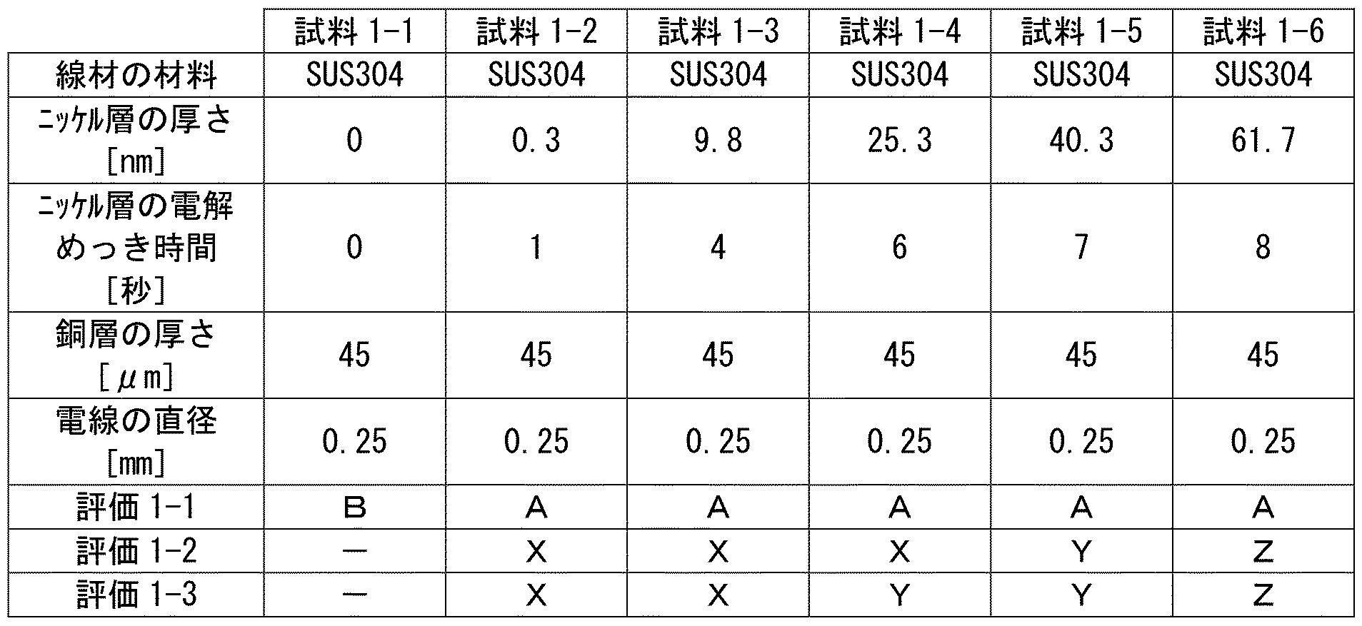
表2に示す結果から、ニッケル層の厚さが0.3nm以上40.3nm以下の範囲内にある試料1-2~試料1-5の電線1においては、ニッケル層の厚さが0.3nm以上40.3nm以下の範囲内にない試料1-1および試料1-6の電線1と比べて、電線1に外部から応力が印加されたときに銅層に割れが発生するのを抑制することができることが確認された。
また、表2に示す結果から、ニッケル層の厚さが0.3nm以上25.3nm以下の範囲内にある試料1-2~試料1-4の電線1においては、ニッケル層の厚さが0.3nm以上25.3nm以下の範囲内にない試料1-1、試料1-5および試料1-6の電線1と比べて、電線1に外部から応力が印加されたときに銅層に割れが発生するのを抑制することができることが確認された。
さらに、表2に示す結果から、ニッケル層の厚さが0.3nm以上9.8nm以下の範囲内にある試料1-2~試料1-3の電線1においては、ニッケル層の厚さが0.3nm以上9.8nm以下の範囲内にない試料1-1および試料1-4~試料1-6の電線1と比べて、電線1に外部から応力が印加されたときに銅層に割れが発生するのを抑制することができることが確認された。
なお、表2に示されるニッケル層の厚さは、日本電子株式会社製の透過型電子顕微鏡「JEM-2100F」により測定された値である。
なお、表2に示されるニッケル層の厚さは、日本電子株式会社製の透過型電子顕微鏡「JEM-2100F」により測定された値である。
<試料2-1~2-5の作製>
上記の(4)銅層の形成工程における銅の電解めっきの電流密度を以下の表3に示す条件としたこと以外は試料1-2の電線と同一の方法および同一の条件で試料2-1~2-4の電線を作製した。また、試料2-5の電線は、硫酸銅の電解めっき浴に添加剤を追加したこと以外は試料2-4の電線と同一の方法および同一の条件で作製された。
上記の(4)銅層の形成工程における銅の電解めっきの電流密度を以下の表3に示す条件としたこと以外は試料1-2の電線と同一の方法および同一の条件で試料2-1~2-4の電線を作製した。また、試料2-5の電線は、硫酸銅の電解めっき浴に添加剤を追加したこと以外は試料2-4の電線と同一の方法および同一の条件で作製された。
<評価2-1>
上記のようにして作製された試料2-1~2-5のそれぞれの電線の一部を縦断面の直径が0.30mmの棒に4~5回巻き付けた。次に、棒に巻き付けた後の試料2-1~2-5の電線の銅層の剥離の評価(評価2-1)を以下の評価基準により行なった。その結果を表3に示す。
上記のようにして作製された試料2-1~2-5のそれぞれの電線の一部を縦断面の直径が0.30mmの棒に4~5回巻き付けた。次に、棒に巻き付けた後の試料2-1~2-5の電線の銅層の剥離の評価(評価2-1)を以下の評価基準により行なった。その結果を表3に示す。
<評価2-2>
試料2-1~2-5のそれぞれの電線の一部を縦断面の直径が0.20mmの棒に4~5回巻き付けたこと以外は評価2-1と同一の方法および同一の条件で試料2-1~2-5の電線の銅層の剥離の評価(評価2-2)を以下の評価基準により行なった。その結果を表3に示す。
試料2-1~2-5のそれぞれの電線の一部を縦断面の直径が0.20mmの棒に4~5回巻き付けたこと以外は評価2-1と同一の方法および同一の条件で試料2-1~2-5の電線の銅層の剥離の評価(評価2-2)を以下の評価基準により行なった。その結果を表3に示す。
<評価2-1および評価2-2の評価基準>
X…銅層の剥離が発生しなかった。
Y…銅層の一部に剥離が発生した。
Z…銅層の全体に剥離が発生した。
X…銅層の剥離が発生しなかった。
Y…銅層の一部に剥離が発生した。
Z…銅層の全体に剥離が発生した。
図12は、評価2-1および評価2-2の評価基準Xの試料2-1~2-5の電線の一例の拡大写真である。図13は、評価2-1および評価2-2の評価基準Yの試料2-1~2-5の電線の一例の拡大写真である。
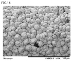
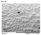
図14は、試料2-2の電線の銅層の外周面(銅層の外周面の算術平均粗さRa=3.4μm)の拡大写真である。図15は、試料2-3の電線の銅層の外周面(銅層の外周面の算術平均粗さRa=1.6μm)の拡大写真である。図16は、試料2-4の電線の銅層の外周面(銅層の外周面の算術平均粗さRa=1.1μm)の拡大写真である。
なお、表3の「算術平均粗さRa[μm]」の欄における算術平均粗さRa[μm]の値は、試料2-1~2-5の電線の銅層の外周面について、株式会社キーエンス製の「VX-K100series」を用いて、JIS B 0601(1994)またはJIS B 0031(1994)に基づいて測定された値である。
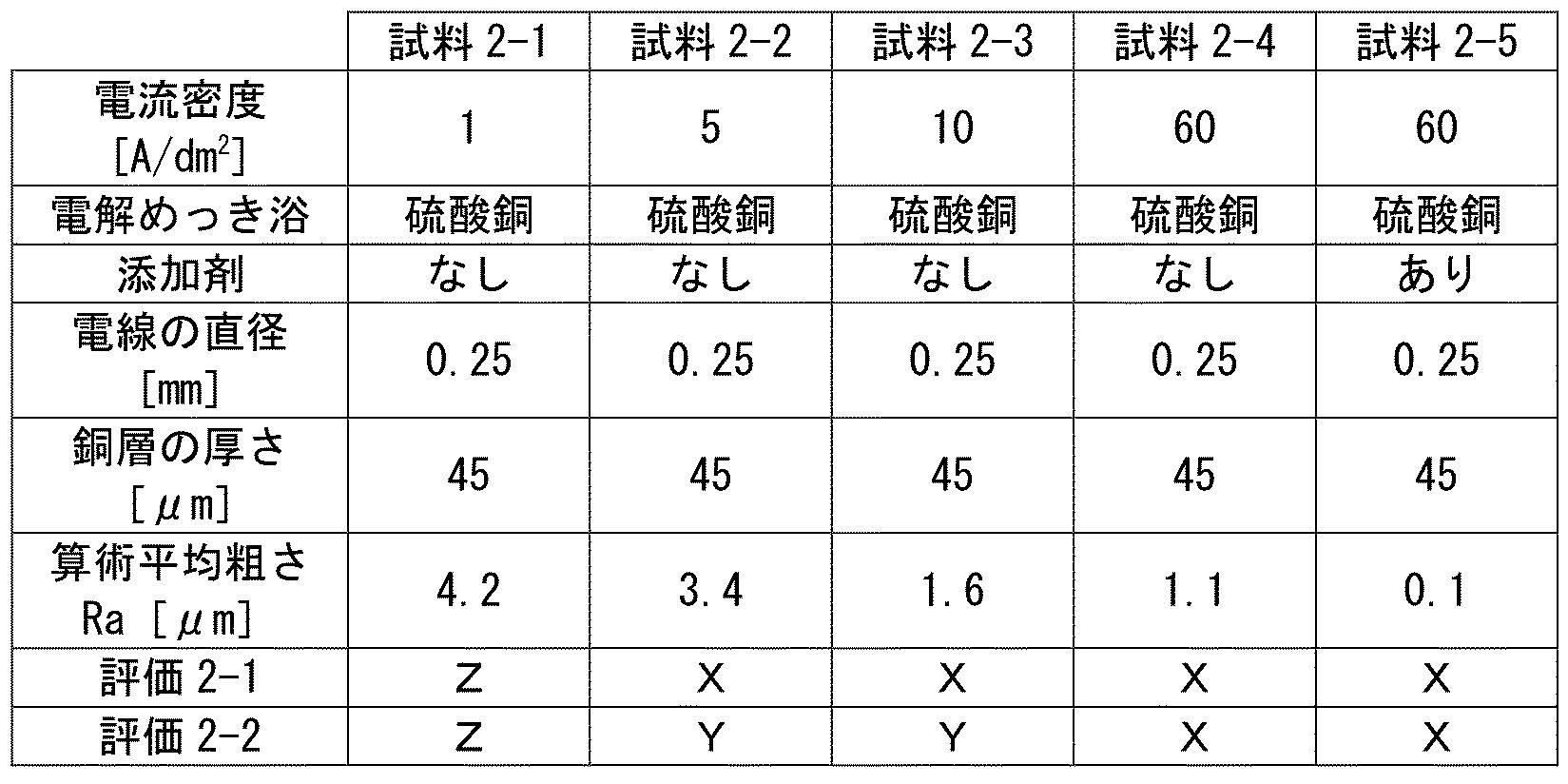
表3に示す結果から、銅層の外周面の算術平均粗さRaが0.1μm以上3.4μm以下の範囲内にある試料2-2~試料2-5の電線においては、銅層の外周面の算術平均粗さRaが0.1μm以上3.4μm以下の範囲内にない試料2-1の電線と比べて、ニッケル層からの銅層の剥離を抑制することできることが確認された。
また、表3に示す結果から、銅層の外周面の算術平均粗さRaが0.1μm以上1.1μm以下の範囲内にある試料2-4~試料2-5の電線においては、銅層の外周面の算術平均粗さRaが0.1μm以上1.1μm以下の範囲内にない試料2-1~試料2-3の電線と比べて、ニッケル層からの銅層の剥離を抑制することできることが確認された。
以上のように実施形態および実施例について説明を行なったが、上述の実施形態および実施例の各構成を適宜組み合わせることも当初から予定している。
今回開示された実施形態および実施例はすべての点で例示であって制限的なものではないと考えられるべきである。本発明の範囲は上記した説明ではなくて請求の範囲によって示され、請求の範囲と均等の意味および範囲内でのすべての変更が含まれることが意図される。
1 電線、1a 端面、1b 長手方向軸、1c 仮想面、2 線材、3 ニッケル層、4 銅層、20a,20b 銅板、21 矢印、31 割れ。
Claims (14)
- 主成分として鉄を含む線材と、
前記線材の外周面上のニッケル層と、
前記ニッケル層の外周面上の銅層と、を備え、
前記ニッケル層の厚さが0.3nm以上40.3nm以下である、電線。 - 前記線材の直径は、0.2mm以上0.3mm以下である、請求項1に記載の電線。
- 前記銅層の厚さは、40μm以上60μm以下である、請求項1または請求項2に記載の電線。
- 前記線材は、ステンレス鋼を含む、請求項1から請求項3のいずれか1項に記載の電線。
- 前記線材は、炭素鋼を含む、請求項1から請求項4のいずれか1項に記載の電線。
- 前記銅層の外周面の算術平均粗さ(Ra)は、0.1μm以上3.4μm以下である、請求項1から請求項5のいずれか1項に記載の電線。
- 前記ニッケル層の厚さは、0.3nm以上25.3nm以下である、請求項1から請求項6のいずれか1項に記載の電線。
- 前記ニッケル層の厚さは、0.3nm以上9.8nm以下である、請求項1から請求項7のいずれか1項に記載の電線。
- 前記電線の一端が端面を有し、
前記端面は、前記電線の長手方向軸に直交する仮想面に対して傾斜する面を有している、請求項1から請求項8のいずれか1項に記載の電線。 - 主成分として鉄を含む線材と、
前記線材の外周面上の銅層と、を備え、
前記銅層の外周面の算術平均粗さ(Ra)は、0.1μm以上3.4μm以下である、電線。 - 主成分として鉄を含む線材と、
前記線材の外周面上の銅層と、を備える電線であって、
前記電線の一端が端面を有し、
前記端面は、前記電線の長手方向軸に直交する仮想面に対して傾斜する面を有する、電線。 - 主成分として鉄を含む線材を準備する工程と、
前記線材の外周面上にニッケル層を形成する工程と、
前記ニッケル層の外周面上に銅層を形成する工程と、を含み、
前記ニッケル層を形成する工程は、前記ニッケル層の厚さが0.3nm以上40.3nm以下となるように前記ニッケル層を形成する工程を含む、電線の製造方法。 - 主成分として鉄を含む線材を準備する工程と、
前記線材の外周面上に銅層を形成する工程と、を含む電線の製造方法であって、
前記電線の製造方法は、
前記電線の一部を加工することによって前記電線に端面を形成する工程をさらに含み、
前記端面を形成する工程は、前記端面が前記電線の長手方向軸に直交する仮想面に対して傾斜する面を有するように前記端面を形成する工程を含む、電線の製造方法。 - 主成分として鉄を含む線材を準備する工程と、
前記線材の外周面上に銅層を形成する工程と、を含む電線の製造方法であって、
前記電線の製造方法は、
前記電線の一部を切断することによって前記電線に端面を形成する工程をさらに含み、
前記端面を形成する工程は、前記端面が前記電線の長手方向軸に直交する仮想面に対して傾斜する面を有するように前記端面を形成する工程を含む、電線の製造方法。
Priority Applications (1)
| Application Number | Priority Date | Filing Date | Title |
|---|---|---|---|
| PCT/JP2021/020001 WO2022249336A1 (ja) | 2021-05-26 | 2021-05-26 | 電線および電線の製造方法 |
Applications Claiming Priority (1)
| Application Number | Priority Date | Filing Date | Title |
|---|---|---|---|
| PCT/JP2021/020001 WO2022249336A1 (ja) | 2021-05-26 | 2021-05-26 | 電線および電線の製造方法 |
Publications (1)
| Publication Number | Publication Date |
|---|---|
| WO2022249336A1 true WO2022249336A1 (ja) | 2022-12-01 |
Family
ID=84228572
Family Applications (1)
| Application Number | Title | Priority Date | Filing Date |
|---|---|---|---|
| PCT/JP2021/020001 Ceased WO2022249336A1 (ja) | 2021-05-26 | 2021-05-26 | 電線および電線の製造方法 |
Country Status (1)
| Country | Link |
|---|---|
| WO (1) | WO2022249336A1 (ja) |
Citations (8)
| Publication number | Priority date | Publication date | Assignee | Title |
|---|---|---|---|---|
| JPS60131996A (ja) * | 1983-12-19 | 1985-07-13 | Furukawa Electric Co Ltd:The | 被メツキステンレス鋼及びその製造方法 |
| JPS6132367A (ja) * | 1984-07-23 | 1986-02-15 | 住友電気工業株式会社 | 素線絶縁ケ−ブルの導体接続方法 |
| JPS6286607A (ja) * | 1985-10-11 | 1987-04-21 | 住友電気工業株式会社 | 高強度、良屈曲性導体 |
| JP2004207080A (ja) * | 2002-12-25 | 2004-07-22 | Sumitomo Electric Ind Ltd | 自動車用導体 |
| JP2010146926A (ja) * | 2008-12-19 | 2010-07-01 | Furukawa Electric Co Ltd:The | 可動接点部品用銀被覆材およびその製造方法 |
| JP2010153069A (ja) * | 2008-12-24 | 2010-07-08 | Sumitomo Electric Ind Ltd | リッツ線アセンブリ |
| JP2011251394A (ja) * | 2010-06-04 | 2011-12-15 | Suzuki Kinzoku Kogyo Kk | 放電加工用電極線 |
| JP2015071221A (ja) * | 2013-09-09 | 2015-04-16 | 住友電工スチールワイヤー株式会社 | ワイヤ放電加工用電極線 |
-
2021
- 2021-05-26 WO PCT/JP2021/020001 patent/WO2022249336A1/ja not_active Ceased
Patent Citations (8)
| Publication number | Priority date | Publication date | Assignee | Title |
|---|---|---|---|---|
| JPS60131996A (ja) * | 1983-12-19 | 1985-07-13 | Furukawa Electric Co Ltd:The | 被メツキステンレス鋼及びその製造方法 |
| JPS6132367A (ja) * | 1984-07-23 | 1986-02-15 | 住友電気工業株式会社 | 素線絶縁ケ−ブルの導体接続方法 |
| JPS6286607A (ja) * | 1985-10-11 | 1987-04-21 | 住友電気工業株式会社 | 高強度、良屈曲性導体 |
| JP2004207080A (ja) * | 2002-12-25 | 2004-07-22 | Sumitomo Electric Ind Ltd | 自動車用導体 |
| JP2010146926A (ja) * | 2008-12-19 | 2010-07-01 | Furukawa Electric Co Ltd:The | 可動接点部品用銀被覆材およびその製造方法 |
| JP2010153069A (ja) * | 2008-12-24 | 2010-07-08 | Sumitomo Electric Ind Ltd | リッツ線アセンブリ |
| JP2011251394A (ja) * | 2010-06-04 | 2011-12-15 | Suzuki Kinzoku Kogyo Kk | 放電加工用電極線 |
| JP2015071221A (ja) * | 2013-09-09 | 2015-04-16 | 住友電工スチールワイヤー株式会社 | ワイヤ放電加工用電極線 |
Similar Documents
| Publication | Publication Date | Title |
|---|---|---|
| JP6380174B2 (ja) | 銀めっき付き銅端子材及び端子 | |
| CN113994439B (zh) | 铜覆钢线、弹簧、绞合线、绝缘电线以及电缆 | |
| US20100247959A1 (en) | Sn-plated copper or sn-plated copper alloy having excellent heat resistance and manufacturing method thereof | |
| JP6060875B2 (ja) | 基板用端子および基板コネクタ | |
| JP2014208904A (ja) | 耐摩耗性に優れる接続部品用導電材料 | |
| WO2015033896A1 (ja) | ワイヤ放電加工用電極線およびその製造方法 | |
| KR20130027469A (ko) | 방전 가공용 전극선 | |
| JP2023150441A (ja) | コネクタ用端子材 | |
| KR102640504B1 (ko) | 도금 선봉 | |
| CN113498543B (zh) | 铝基线材、绞合线以及铝基线材的制造方法 | |
| US10998108B2 (en) | Electrical contact material, method of producing an electrical contact material, and terminal | |
| WO2022249336A1 (ja) | 電線および電線の製造方法 | |
| US11810691B2 (en) | Aluminum base wire | |
| JP2011219840A (ja) | サスペンションワイヤ | |
| JP5761400B1 (ja) | コネクタピン用線材、その製造方法及びコネクタ | |
| CN110603114A (zh) | 线放电加工用电极线 | |
| JP3312235B2 (ja) | ベリリウム銅合金ばね材およびその製造方法 | |
| JP2003291030A (ja) | ワイヤ放電加工用電極線 | |
| JP5076088B2 (ja) | Snめっき銅基板、Snめっき銅基板の製造方法、およびこれを用いたリードフレームおよびコネクタ端子 | |
| WO2019031549A1 (ja) | 銀皮膜付端子材及び銀皮膜付端子 | |
| WO2023047854A1 (ja) | 線材および線材の製造方法 | |
| JP2024101458A (ja) | ニッケルめっき材及びタブリード用リード導体 | |
| JP2003059361A (ja) | エナメル線用塗装ダイおよびその製造方法 | |
| JP2002172529A (ja) | ワイヤ放電加工用電極線の製造方法 | |
| JP2005138236A (ja) | 放電加工用電極線の製造方法及び放電加工用電極線 |
Legal Events
| Date | Code | Title | Description |
|---|---|---|---|
| 121 | Ep: the epo has been informed by wipo that ep was designated in this application |
Ref document number: 21942990 Country of ref document: EP Kind code of ref document: A1 |
|
| NENP | Non-entry into the national phase |
Ref country code: DE |
|
| 122 | Ep: pct application non-entry in european phase |
Ref document number: 21942990 Country of ref document: EP Kind code of ref document: A1 |
|
| NENP | Non-entry into the national phase |
Ref country code: JP |