WO2022244166A1 - 温度推定装置及びコンバータシステム - Google Patents
温度推定装置及びコンバータシステム Download PDFInfo
- Publication number
- WO2022244166A1 WO2022244166A1 PCT/JP2021/019067 JP2021019067W WO2022244166A1 WO 2022244166 A1 WO2022244166 A1 WO 2022244166A1 JP 2021019067 W JP2021019067 W JP 2021019067W WO 2022244166 A1 WO2022244166 A1 WO 2022244166A1
- Authority
- WO
- WIPO (PCT)
- Prior art keywords
- value
- temperature
- current
- junction temperature
- power semiconductor
- Prior art date
- Legal status (The legal status is an assumption and is not a legal conclusion. Google has not performed a legal analysis and makes no representation as to the accuracy of the status listed.)
- Ceased
Links
Images


Classifications
-
- H—ELECTRICITY
- H02—GENERATION; CONVERSION OR DISTRIBUTION OF ELECTRIC POWER
- H02M—APPARATUS FOR CONVERSION BETWEEN AC AND AC, BETWEEN AC AND DC, OR BETWEEN DC AND DC, AND FOR USE WITH MAINS OR SIMILAR POWER SUPPLY SYSTEMS; CONVERSION OF DC OR AC INPUT POWER INTO SURGE OUTPUT POWER; CONTROL OR REGULATION THEREOF
- H02M1/00—Details of apparatus for conversion
- H02M1/32—Means for protecting converters other than automatic disconnection
- H02M1/327—Means for protecting converters other than automatic disconnection against abnormal temperatures
-
- H—ELECTRICITY
- H02—GENERATION; CONVERSION OR DISTRIBUTION OF ELECTRIC POWER
- H02M—APPARATUS FOR CONVERSION BETWEEN AC AND AC, BETWEEN AC AND DC, OR BETWEEN DC AND DC, AND FOR USE WITH MAINS OR SIMILAR POWER SUPPLY SYSTEMS; CONVERSION OF DC OR AC INPUT POWER INTO SURGE OUTPUT POWER; CONTROL OR REGULATION THEREOF
- H02M5/00—Conversion of AC power input into AC power output, e.g. for change of voltage, for change of frequency, for change of number of phases
- H02M5/40—Conversion of AC power input into AC power output, e.g. for change of voltage, for change of frequency, for change of number of phases with intermediate conversion into DC
- H02M5/42—Conversion of AC power input into AC power output, e.g. for change of voltage, for change of frequency, for change of number of phases with intermediate conversion into DC by static converters
- H02M5/44—Conversion of AC power input into AC power output, e.g. for change of voltage, for change of frequency, for change of number of phases with intermediate conversion into DC by static converters using discharge tubes or semiconductor devices to convert the intermediate DC into AC
- H02M5/453—Conversion of AC power input into AC power output, e.g. for change of voltage, for change of frequency, for change of number of phases with intermediate conversion into DC by static converters using discharge tubes or semiconductor devices to convert the intermediate DC into AC using devices of a triode or transistor type requiring continuous application of a control signal
- H02M5/458—Conversion of AC power input into AC power output, e.g. for change of voltage, for change of frequency, for change of number of phases with intermediate conversion into DC by static converters using discharge tubes or semiconductor devices to convert the intermediate DC into AC using devices of a triode or transistor type requiring continuous application of a control signal using semiconductor devices only
- H02M5/4585—Conversion of AC power input into AC power output, e.g. for change of voltage, for change of frequency, for change of number of phases with intermediate conversion into DC by static converters using discharge tubes or semiconductor devices to convert the intermediate DC into AC using devices of a triode or transistor type requiring continuous application of a control signal using semiconductor devices only having a rectifier with controlled elements
-
- H—ELECTRICITY
- H02—GENERATION; CONVERSION OR DISTRIBUTION OF ELECTRIC POWER
- H02M—APPARATUS FOR CONVERSION BETWEEN AC AND AC, BETWEEN AC AND DC, OR BETWEEN DC AND DC, AND FOR USE WITH MAINS OR SIMILAR POWER SUPPLY SYSTEMS; CONVERSION OF DC OR AC INPUT POWER INTO SURGE OUTPUT POWER; CONTROL OR REGULATION THEREOF
- H02M7/00—Conversion of AC power input into DC power output; Conversion of DC power input into AC power output
- H02M7/02—Conversion of AC power input into DC power output without possibility of reversal
- H02M7/04—Conversion of AC power input into DC power output without possibility of reversal by static converters
- H02M7/12—Conversion of AC power input into DC power output without possibility of reversal by static converters using discharge tubes with control electrode or semiconductor devices with control electrode
- H02M7/21—Conversion of AC power input into DC power output without possibility of reversal by static converters using discharge tubes with control electrode or semiconductor devices with control electrode using devices of a triode or transistor type requiring continuous application of a control signal
- H02M7/217—Conversion of AC power input into DC power output without possibility of reversal by static converters using discharge tubes with control electrode or semiconductor devices with control electrode using devices of a triode or transistor type requiring continuous application of a control signal using semiconductor devices only
- H02M7/219—Conversion of AC power input into DC power output without possibility of reversal by static converters using discharge tubes with control electrode or semiconductor devices with control electrode using devices of a triode or transistor type requiring continuous application of a control signal using semiconductor devices only in a bridge configuration
-
- H—ELECTRICITY
- H02—GENERATION; CONVERSION OR DISTRIBUTION OF ELECTRIC POWER
- H02M—APPARATUS FOR CONVERSION BETWEEN AC AND AC, BETWEEN AC AND DC, OR BETWEEN DC AND DC, AND FOR USE WITH MAINS OR SIMILAR POWER SUPPLY SYSTEMS; CONVERSION OF DC OR AC INPUT POWER INTO SURGE OUTPUT POWER; CONTROL OR REGULATION THEREOF
- H02M7/00—Conversion of AC power input into DC power output; Conversion of DC power input into AC power output
- H02M7/66—Conversion of AC power input into DC power output; Conversion of DC power input into AC power output with possibility of reversal
- H02M7/68—Conversion of AC power input into DC power output; Conversion of DC power input into AC power output with possibility of reversal by static converters
- H02M7/72—Conversion of AC power input into DC power output; Conversion of DC power input into AC power output with possibility of reversal by static converters using discharge tubes with control electrode or semiconductor devices with control electrode
- H02M7/79—Conversion of AC power input into DC power output; Conversion of DC power input into AC power output with possibility of reversal by static converters using discharge tubes with control electrode or semiconductor devices with control electrode using devices of a triode or transistor type requiring continuous application of a control signal
- H02M7/797—Conversion of AC power input into DC power output; Conversion of DC power input into AC power output with possibility of reversal by static converters using discharge tubes with control electrode or semiconductor devices with control electrode using devices of a triode or transistor type requiring continuous application of a control signal using semiconductor devices only
Definitions
- the present invention relates to a temperature estimation device and a converter system.
- a converter and an inverter are power conversion devices that convert DC power to AC power or power conversion from AC power to DC power.
- the AC power supplied from the AC power supply is converted into DC power by a converter and sent to the DC link.
- the DC power in the DC link is converted into AC power by an inverter, and this AC power is supplied as driving power to the motor provided for each drive shaft.
- the DC link refers to a circuit portion that electrically connects the DC output side of the converter and the DC input side of the inverter. It is sometimes called a "DC intermediate circuit".
- the method of grasping the temperature of the power semiconductor element or the vicinity of the power semiconductor element in the converter and inverter the method of estimating the junction temperature of the power semiconductor element by calculation, the case temperature of the power semiconductor element (mold surface temperature and base plate surface temperature)
- the method of measuring the temperature a method of measuring the temperature of a radiator in contact with the power semiconductor element, and the like.
- the method of estimating the junction temperature of the power semiconductor element by calculation is based on the current value flowing through the power semiconductor element and the thermal equivalent circuit, and the temperature of the junction part of the power semiconductor element is calculated by calculation processing by the arithmetic processing unit. It estimates a certain junction temperature.
- a converter that converts AC voltage to DC voltage
- an inverter that converts the DC voltage to AC voltage and drives a motor
- a speed control unit that generates a torque command based on the speed command and the motor speed
- the torque command and a torque control unit that generates a PWM signal based on the motor current and drives the inverter
- a current detection unit that detects the motor current
- an inverter temperature detection unit that detects the temperature of the inverter and generates an inverter temperature signal
- the overload protection section receives the motor current from the inverter.
- a junction temperature estimating unit that estimates a junction temperature based on the power element estimated loss and the inverter temperature; and a motor loss that is estimated from the motor current and the motor speed.
- a motor control device characterized by comprising a section and a section (see, for example, Patent Document 1).
- an elevator control device having an inverter device that drives and controls an AC motor that vertically drives an elevator car, a switching loss calculator that calculates an instantaneous switching loss when switching a semiconductor power element in the inverter device, an on-loss calculator that calculates an instantaneous on-loss when the semiconductor power element is turned on and a constant current is flowing;
- a switching loss calculator that calculates an instantaneous switching loss when switching a semiconductor power element in the inverter device
- an on-loss calculator that calculates an instantaneous on-loss when the semiconductor power element is turned on and a constant current is flowing
- a temperature detecting means for detecting the temperature of a case in which the power element is mounted; calculating an increase in temperature difference between the junction temperature of each power element and the case temperature; A temperature estimating means for estimating the junction temperature of each power element, the junction temperature of each power element, and the allowable operating temperature of each power element are compared and calculated on the basis of the calculation results obtained by adding the temperatures of the case.
- overheating abnormality determining means for determining that the power element is in an overheated state and outputting an overheating abnormality signal when the junction temperature is higher than the allowable operating temperature as a result of the calculation; and power cutoff signal output means for outputting a power cutoff signal for cutting off the gate of the power element when an overheating abnormality signal is input (for example, , see Patent Document 3.).
- the voltage or current unbalance rate is small, so there is little variation in the junction temperatures of the multiple power semiconductor devices in the converter. Therefore, even if the junction temperature of the power semiconductor element is estimated based on one thermal equivalent circuit for the purpose of reducing the ratio of the junction temperature estimation process (for example, the CPU usage rate) in the arithmetic processing of the arithmetic processing unit, the calculation There is little divergence between the estimated value of the junction temperature and the true value of the junction temperature of each power semiconductor device.
- the junction temperature estimation process of the power semiconductor element based on one thermal equivalent circuit allows the arithmetic processing unit to calculate It is possible to achieve both a reduction in processing load and highly accurate temperature estimation.
- the voltage or current unbalance rate will increase. Variation in individual junction temperatures of a plurality of existing power semiconductor devices also increases.
- the calculated estimated value of the junction temperature is It deviates greatly from the true value of the junction temperature for That is, a power semiconductor device appears that has a true value of junction temperature that greatly deviates from the calculated estimated value of junction temperature.
- a temperature estimation device capable of calculating the junction temperature estimation value of the power semiconductor element provided in the converter with high accuracy, and the same. Realization of a converter system that includes
- a temperature estimation device that calculates an estimated junction temperature value of a power semiconductor element provided in a converter that performs power conversion between AC power on a three-phase AC power supply side and DC power on a DC side is a current detection unit that detects the value of the current flowing through the power semiconductor element, a provisional junction temperature value calculated based at least on the value of the current detected by the current detection unit, and an impedance of the three-phase AC power supply connected to the converter.
- a junction temperature estimating unit that calculates an estimated junction temperature of the power semiconductor element based on the balance ratio.
- the converter system is provided with the temperature estimating device and a power semiconductor element, and the power semiconductor element turns on and off to generate alternating current power on the three-phase alternating current power supply side and direct current power on the direct current side.
- a converter that performs power conversion with electric power, and the junction temperature estimator calculates an estimated junction temperature value of the power semiconductor element.
- the unbalance factor of the three-phase AC power supply when the power quality of the three-phase AC power supply connected to the converter is poor, or when an abnormality such as an open phase occurs in the three-phase AC power supply, the unbalance factor of the three-phase AC power supply It is possible to realize a temperature estimating device and a converter system including the same that can calculate the junction temperature estimated value of the power semiconductor element provided in the converter with high accuracy even when the temperature is high. That is, according to one aspect of the present disclosure, since the ratio of the junction temperature estimation process (for example, the CPU usage rate) in the arithmetic processing of the arithmetic processing device is reduced, other arithmetic operations other than the temperature estimation processing are performed in the arithmetic processing device. The influence on processing can be suppressed.
- the ratio of the junction temperature estimation process for example, the CPU usage rate
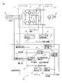
- FIG. 1 is a diagram illustrating a temperature estimating device and a converter system including the same according to first and fourth embodiments of the present disclosure
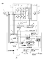
- FIG. FIG. 4 is a diagram showing a modification of the unbalance rate calculator in the temperature estimating device and the converter system including the same according to the first embodiment of the present disclosure
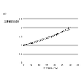
- FIG. 10 is a diagram illustrating the relationship between the unbalance rate k calculated by the second calculation method of the temperature compensation coefficient and the temperature compensation coefficient A
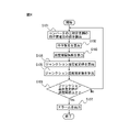
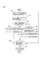
- 4 is a flow chart showing the operation flow of the temperature estimation device according to the first embodiment of the present disclosure
- FIG. 6 is a diagram showing a temperature estimating device and a converter system including the same according to a second embodiment of the present disclosure
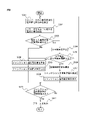
- 9 is a flow chart showing the operation flow of the temperature estimation device according to the second embodiment of the present disclosure
- FIG. 10 is a diagram illustrating a temperature estimating device and a converter system including the same according to a third embodiment of the present disclosure
- FIG. 11 is a flow chart showing an operation flow of a temperature estimation device according to a fourth embodiment of the present disclosure
- FIG. FIG. 11 is a flow chart showing an operation flow of a temperature estimation device according to a fourth embodiment of the present disclosure
- the load on the DC side of the converter system including the temperature estimation device includes a set of an inverter and an AC motor, a DC motor, and the like.
- Machines provided with AC motors or DC motors include, for example, machine tools, press machines, injection molding machines, industrial machines, and various robots.
- the type of AC motor is not particularly limited, and may be, for example, an induction motor or a synchronous motor.
- the number of phases of the AC motor does not particularly limit the embodiments of the present disclosure, and may be three-phase or single-phase, for example. Note that the following description is similarly applicable to a case where a DC motor is provided as a load on the DC side of a converter system that includes a temperature estimating device according to an embodiment of the present disclosure.
- FIG. 1 is a diagram showing a temperature estimating device according to first and fourth embodiments of the present disclosure and a converter system including the same.
- the temperature estimating device shown in FIG. 1 and the connection relationship of each element in the converter system including the same can also be applied to a fourth embodiment described later.
- the converter system 100 includes a temperature estimation device 1 according to the first embodiment of the present disclosure, a converter 2, and a converter control device 3.
- a three-phase AC power supply 4 is connected to the AC side of the converter 2 via, for example, a magnetic contactor (MCC) and a three-phase AC reactor.
- MCC magnetic contactor
- Examples of the three-phase AC power supply 4 include a three-phase AC 400V power supply, a three-phase AC 200V power supply, a three-phase AC 600V power supply, and the like.
- the converter 2 in the converter system 100 includes a three-phase bridge circuit 31, a smoothing capacitor 32, a DC link capacitor 33, a precharging circuit 34, and a temperature detection element 35.
- the three-phase bridge circuit 31 in the converter 2 can convert AC power to DC power. rectifier circuit, etc.
- the three-phase bridge circuit 31 is a PWM switching control type rectifier circuit or a synchronous rectification type rectifier circuit.
- the three-phase bridge circuit 31 has three legs corresponding to each of the three phases. Each leg has an upper arm and a lower arm.
- each upper arm and each lower arm of the three-phase bridge circuit 31 includes a semiconductor switching element and an anti-parallel semiconductor switching element.
- a power semiconductor component is provided comprising a diode connected to the Examples of semiconductor switching devices include IGBTs, FETs, thyristors, GTOs, and transistors.
- each upper arm and each lower arm of the three-phase bridge circuit 31 is provided with a power semiconductor element composed of a diode.
- the smoothing capacitor 32 is provided on the DC side of the three-phase bridge circuit 31 and has the function of suppressing the pulsation of the DC output from the three-phase bridge circuit 31 .
- Examples of the smoothing capacitor 32 include, for example, an electrolytic capacitor and a film capacitor.
- the DC link capacitor 33 is provided between the smoothing capacitor 32 and the DC side of the inverter 5, and has a function of accumulating DC power.
- Examples of the DC link capacitor 33 include, for example, electrolytic capacitors and film capacitors.
- a preliminary charging circuit (initial charging circuit) 34 is provided for preliminary charging (initial charging) of the DC link capacitor 33 before the inverter 5 starts operating.
- the precharging circuit 34 has a switch that opens and closes the electric path between the three-phase bridge circuit 31 and the DC link capacitor 33, and a charging resistor that is connected in parallel with the switch. The switch is opened (turned off) during the pre-charging period from immediately after the inverter 5 is activated (immediately after the power is turned on) to before the normal operation of the inverter 5 starts.
- the switch Since the switch is kept open during the pre-charging period, the current output from the three-phase bridge circuit 31 flows into the DC link capacitor 33 as a charging current through the charging resistor, and the DC link capacitor 33 is charged (pre-charged). ) is done. During the pre-charging period, the current output from the three-phase bridge circuit 31 flows through the charging resistor, thus preventing the occurrence of rush current.
- the switch When the DC link capacitor 33 is charged to a predetermined voltage, the switch is switched from open to closed, completing precharging by the precharging circuit 34 . After the preliminary charging is completed, the current output from the three-phase bridge circuit 31 flows through the closed switch to the inverter 5 and the DC link capacitor 33 connected to the DC link.
- the temperature detection element 35 is an element that is provided near the power semiconductor element and whose output changes as the temperature of the temperature detection element 35 changes. A signal output from the temperature detection element 35 is sent to the ambient temperature detection section 14 in the temperature estimation device 1, which will be described later.
- Examples of the temperature detection element 35 include, for example, a PTC thermistor, an NTC thermistor, and a platinum resistance thermometer.
- the converter control device 3 in the converter system 100 includes a switching control section 41 and a DC link section voltage detection section 42 .
- the DC link section voltage detection section 42 detects the DC link capacitor voltage value, which is the potential difference between both ends of the DC link capacitor 33 .
- This capacitor voltage value corresponds to the DC link voltage value. That is, the value of the potential difference between the positive potential appearing at the positive terminal on the DC output side of the three-phase bridge circuit 31 and the negative potential appearing at the negative terminal on the DC output side of the three-phase bridge circuit 31 is the DC link capacitor voltage. value.
- the DC link capacitor voltage value detected by the DC link section voltage detection section 42 is sent to the switching control section 41 and also sent to a host control device (not shown) for controlling the inverter 5 .
- the switching control unit 41 receives a drive command from a host controller (not shown), a DC link capacitor voltage value detected by a DC link voltage detection unit 42, and a converter 2 detected by a current detection unit 11, which will be described later. Based on the value of the input current (the value of the current flowing through the power semiconductor element) and the value of the voltage across the terminals on the three-phase AC power supply side of the converter 2 detected by the voltage detection unit 13 described later, the three-phase bridge A switching command is generated to instruct the semiconductor switching element of each power semiconductor element in the circuit 31 to turn on and off. The generated switching command is sent to a drive circuit (not shown) for the semiconductor switching element. The drive circuit applies a gate voltage to each semiconductor switching element for turning on/off the semiconductor switching element according to the content of the switching command.
- the current detection unit 11 and the voltage detection unit 13 are shared by the temperature estimation device 1 and the converter control device 3 .
- temperature estimation device 1 and converter control device 3 may be provided with separate current detection units and voltage detection units.
- An arithmetic processing unit (processor) is provided in the converter control device 3 .
- This arithmetic processing unit has the switching control section 41 and the DC link section voltage detection section 42 described above.
- Each of these units of the arithmetic processing unit is, for example, a functional module realized by a computer program executed on the processor.
- the switching control section 41 and the DC link section voltage detection section 42 are constructed in the form of a computer program, the function of each section can be realized by operating the arithmetic processing unit according to this computer program.
- a computer program for executing each process of the switching control section 41 and the DC link section voltage detection section 42 is provided in a form recorded in a computer-readable recording medium such as a semiconductor memory, a magnetic recording medium, or an optical recording medium.
- the switching control section 41 and the DC link section voltage detection section 42 may be realized as a semiconductor integrated circuit into which a computer program for realizing the function of each section is written.
- An inverter 5 is connected to the DC side of the converter 2 .
- the inverter 5 is composed of a switching element and a diode bridge circuit connected in antiparallel thereto. Examples of switching elements include IGBTs, FETs, thyristors, GTOs, and transistors, but other semiconductor elements may also be used.
- the motor 6 is a three-phase AC motor, so the inverter 5 is configured with a three-phase bridge circuit. If the motor 6 is a single-phase AC motor, the inverter 5 is configured with a single-phase bridge circuit.
- the on/off operation of internal switching elements is PWM-controlled based on commands from a host control device (not shown), thereby converting DC power in the DC link into AC power to drive the motor 6 on the AC input/output side. , the AC power regenerated by the deceleration of the motor 6 is converted into DC power and returned to the DC link.
- the motor 6 has its speed, torque, or rotor position controlled based on the AC power supplied from the inverter 5 .
- a host controller that controls the inverter 5 may be composed of a combination of an analog circuit and an arithmetic processing unit, or may be composed of only an arithmetic processing unit. Arithmetic processing devices that can constitute a host controller that controls the inverter 5 include, for example, ICs, LSIs, CPUs, MPUs, and DSPs.
- the temperature estimation device 1 calculates the junction temperature estimated value of the power semiconductor element provided in the three-phase bridge circuit 31 inside the converter 2 .
- Temperature estimating device 1 includes current detector 11 , junction temperature estimator 12 , voltage detector 13 , ambient temperature detector 14 , temperature comparator 15 , and alarm output unit 16 .
- the current detection unit 11 detects the value of the current flowing through the power semiconductor elements provided in the three-phase bridge circuit 31 of the converter 2 (the value of the current input to the converter 2).
- the current value detected by the current detection unit 11 is sent to the provisional value calculation unit 23 in the junction temperature estimation unit 12 and the switching control unit 41 in the converter control device 3 .
- Current detection unit 11 may be shared with the current detection unit provided in converter control device 3 .
- the voltage detection unit 13 detects the value of the inter-terminal voltage (line voltage) on the three-phase AC power supply 4 side of the converter 2 .
- the value of the inter-terminal voltage detected by voltage detection unit 13 is sent to provisional value calculation unit 23 and unbalance rate calculation unit 21 in junction temperature estimation unit 12 and switching control unit 41 in converter control device 3 .
- Voltage detection unit 13 may be shared with the voltage detection unit provided in converter control device 3 .
- the ambient temperature detection unit 14 detects the ambient temperature of the power semiconductor element based on the signal sent from the temperature detection element 35 provided near the power semiconductor element.
- the ambient temperature of the power semiconductor element detected by the ambient temperature detector 14 is sent to the provisional value calculator 23 in the junction temperature estimator 12 .
- junction temperature estimator 12 calculates the power based on the junction temperature provisional value calculated based at least on the value of the current detected by current detector 11 and the unbalance rate of three-phase AC power supply 4 connected to converter 2. A junction temperature estimate of a semiconductor device is calculated. Therefore, the junction temperature estimator 12 has an unbalance rate calculator 21 , a temperature compensation coefficient calculator 22 , a provisional value calculator 23 , and an estimated value calculator 24 .
- the provisional value calculation unit 23 calculates the current value detected by the current detection unit 11, the terminal voltage value detected by the voltage detection unit 13, and the ambient temperature of the power semiconductor element detected by the ambient temperature detection unit 14. Based on this, the provisional junction temperature value of the power semiconductor element is calculated.
- the junction temperature provisional value is the value of the junction temperature estimated when the three-phase AC power supply 4 is in equilibrium, that is, the value estimated without considering the unbalance rate of the three-phase AC power supply 4 .
- a provisional junction temperature value T j1 of the power semiconductor element can be expressed as shown in Equation (1).
- W be the power generated by the current flowing through the power semiconductor element.
- the predetermined unit reference power of the power semiconductor element is W 0
- the temperature rise rate per unit reference power W 0 of the power semiconductor element is defined as " ⁇ T/W 0 " (constant).
- Ta is the ambient temperature of the power semiconductor element detected by the ambient temperature detection unit 14
- ⁇ is the thermal time constant, and the time during which power is generated in the power semiconductor element (current is not flowing in the power semiconductor element time) is t.
- the ambient temperature Ta of the power semiconductor element in Equation 1 is substantially constant
- setting the ambient temperature Ta of the power semiconductor element in Equation 1 as a constant allows the ambient temperature
- the temperature detection section 14 and the temperature detection element 35 may be omitted.
- the unbalance rate calculator 21 calculates the unbalance rate of the three-phase AC power supply 4 .
- the unbalance rate calculator 21 calculates the voltage unbalance rate of the three-phase AC power supply 4 based on the value of the terminal voltage (line voltage) detected by the voltage detector 13. do.
- the unbalance rate of the voltage of the three-phase AC power supply 4 can be calculated according to a known formula.
- two methods for calculating the unbalance rate of the voltage of the three-phase AC power supply 4 are listed as examples.
- the sources of the two calculation methods are the website of the Japan Electrical Engineers Association (https://jeea.or.jp/course/contents/05102/).
- the first method of calculating the unbalance rate of the voltage of the three-phase AC power supply 4 is as follows.
- the inter-terminal voltage average value E avg can be expressed as shown in Equation 2.
- the positive-sequence voltage E 1 can be expressed as in Equation 3.
- the negative-sequence voltage E 2 can be expressed as in Equation 4.
- the three-phase AC power supply 4 voltage unbalance rate k can be expressed as in Equation 5.
- the second method of calculating the unbalance rate of the voltage of the three-phase AC power supply 4 is as follows.
- Equation 2 the terminal voltage average value E avg is given by Equation 2 above.
- Equation (6) the maximum value E diffmax of the absolute values of the differences between the terminal voltages ERS , E ST and E TR and the terminal voltage average value E avg.
- Equation 7 the three-phase AC power supply 4 can be expressed as Equation 7.
- the unbalance rate calculation unit 21 calculates the voltage unbalance rate of the three-phase AC power supply 4 based on the value of the terminal voltage detected by the voltage detection unit 13, for example, according to Equation 5 or Equation 7 described above. .
- the unbalance rate calculation unit 21 calculates the unbalance rate of the three-phase AC power supply 4 based on the value of the current detected by the current detection unit 11 (the value of the current input to the converter 2).
- the current imbalance rate of the power supply 4 may be calculated.
- FIG. 2 is a diagram showing a modification of the unbalance rate calculator in the temperature estimating device and the converter system including the same according to the first embodiment of the present disclosure.
- the current value detected by the current detector 11 is sent to the unbalance rate calculator 21 .
- the unbalance rate calculator 21 calculates the current unbalance rate of the three-phase AC power supply 4 based on the current value detected by the current detector 11 .
- the unbalance rate of the three-phase AC power supply 4 calculated by the unbalance rate calculator 21 is sent to the temperature compensation coefficient calculator 22 .
- a temperature compensation coefficient calculator 22 calculates a temperature compensation coefficient based on the unbalance rate.
- the temperature compensation coefficient calculated by the temperature compensation coefficient calculator 22 is sent to the estimated value calculator 24 .
- the estimated value calculator 24 outputs a value obtained by multiplying the junction temperature provisional value and the temperature compensation coefficient as the junction temperature estimated value of the power semiconductor element.
- junction temperature provisional value the junction temperature provisional value
- temperature compensation coefficient the junction temperature estimated value
- the junction temperature provisional value calculated by the provisional value calculation unit 23 according to Equation 1 is the value of the junction temperature estimated when the three-phase AC power supply 4 is balanced (not unbalanced). Calculated according to Equation 1 based on the value of the current detected by the current detection unit 11 and the value of the voltage detected by the voltage detection unit 13 under the condition that the three-phase AC power supply 4 is balanced (not unbalanced) Since the provisional junction temperature value is a value close to the true value of the junction temperature, even if the provisional value of the junction temperature is estimated as the junction temperature of the power semiconductor element as it is (that is, even if it is used as the junction temperature estimation value), there is no error. Few.
- the junction calculated according to Equation 1 based on the current value detected by the current detection unit 11 and the voltage value detected by the voltage detection unit 13 under the condition that the unbalance rate of the three-phase AC power supply 4 is large The provisional temperature value deviates greatly from the true value of the junction temperature for some of the plurality of power semiconductor devices. Therefore, in the first embodiment of the present disclosure, the divergence between the junction temperature provisional value calculated by the provisional value calculation unit 23 and the true value of the junction temperature under the condition that the unbalance rate of the three-phase AC power supply 4 is large is A temperature compensation coefficient that reflects the unbalance rate of the three-phase AC power supply 4 is calculated as a parameter for reducing the junction temperature of the power semiconductor device. Confirm as a value.
- the first method of calculating the temperature compensation coefficient is as follows.
- the unbalance rate k is calculated by the second method of calculating the unbalance rate of the voltage of the three-phase AC power supply 4 described above.
- ERS is the minimum value among the inter-terminal voltages ERS , EST , and ETR in Equation 6, Equation 8 holds.
- Equation 9 is obtained.
- Equation 10 The power W RS generated in the R-phase or S-phase power semiconductor element when the voltage E RS is applied between the R-phase and the S-phase when the voltage of the three-phase AC power supply 4 is unbalanced is given by Equation 10. can be expressed as
- Equation 11 the power W RS generated in the R-phase or S-phase power semiconductor element when the voltage E RS is applied between the R-phase and the S-phase when the voltage of the three-phase AC power supply 4 is balanced is given by Equation 11: can be expressed as
- Equation 11 If the power W RS when the voltage of the three-phase AC power supply 4 shown in Equation 11 is balanced is multiplied by the coefficient A shown in Equation 12, the power W RS when the voltage of the three-phase AC power supply 4 is unbalanced shown in Equation 10 is I know you can get it.
- the coefficient A shown in Equation 12 is used to reduce the divergence between the junction temperature provisional value calculated by the provisional value calculation unit 23 and the true value of the junction temperature under the condition that the unbalance rate of the three-phase AC power supply 4 is large. Used as a temperature compensation coefficient. For example, when the unbalance rate k is 0%, the temperature compensation coefficient A is 1.
- the temperature compensation coefficient calculator 22 calculates the temperature compensation coefficient A using the unbalance rate k calculated by the unbalance rate calculator 21 according to Equation 12, and sends the temperature compensation coefficient A to the estimated value calculator 24. .
- the estimated value calculation unit 24 estimates the junction temperature of the power semiconductor element by multiplying the junction temperature provisional value shown in Equation 1 by the temperature compensation coefficient A calculated by the temperature compensation coefficient calculation unit 22, for example. Output as a value.
- the second method of calculating the temperature compensation coefficient is as follows.
- a second method of calculating the temperature compensation coefficient is an experimental three-phase AC power supply capable of outputting a line-to-line voltage with an arbitrary unbalance rate of 0% to 100% through experiments prior to the actual operation of converter system 100. is operated to obtain the relational expression between the unbalance rate and the temperature compensation coefficient.
- the junction temperature of each power semiconductor element in the three-phase bridge circuit 31 was actually measured by outputting a line voltage with a specific unbalance rate between 0% and 100% from the experimental three-phase AC power supply.
- the temperature compensation coefficient A for the particular unbalance rate is calculated.
- FIG. 3 is a diagram illustrating the relationship between the unbalance rate k calculated by the second calculation method of the temperature compensation coefficient and the temperature compensation coefficient A.
- black circles indicate temperature compensation coefficients A corresponding to unbalance ratios k of 0% to 30% obtained by experiments.
- An approximate expression representing the relationship between the unbalance rate k and the temperature compensation coefficient A is obtained from the values of the unbalance rate k and the temperature compensation coefficient A obtained by experiment.
- the relationship between the unbalance rate k and the temperature compensation coefficient A is obtained by linear approximation (linear function), but a function other than the linear function may be used as the approximate expression.
- the approximation expression representing the relationship between the unbalance rate k and the temperature compensation coefficient A may be calculated with one interval from 0% to 100% of the unbalance rate.
- the range from 0% to 100% of the unbalance rate may be divided into a plurality of sections, and an approximation expression showing the relationship between the unbalance rate k and the temperature compensation coefficient A may be obtained for each section.
- An approximate expression representing the relationship between the unbalance rate k and the temperature compensation coefficient A obtained by experiment is stored in advance in the temperature compensation coefficient calculator 22 .
- the temperature compensation coefficient calculation unit 22 calculates the temperature compensation coefficient A corresponding to the unbalance rate k calculated by the unbalance rate calculation unit 21 according to the approximate expression, and sends the temperature compensation coefficient A to the estimated value calculation unit 24. .
- the estimated value calculation unit 24 estimates the junction temperature of the power semiconductor element by multiplying the junction temperature provisional value shown in Equation 1 by the temperature compensation coefficient A calculated by the temperature compensation coefficient calculation unit 22, for example. Output as a value.
- the junction temperature estimated value of the power semiconductor element is obtained by multiplying the junction temperature provisional value shown in Equation 1 by the temperature compensation coefficient A calculated by the temperature compensation coefficient calculator 22 . That is, the junction temperature estimated value T j2 of the power semiconductor element can be expressed as shown in Equation (13).
- the electric power W generated in the power semiconductor element is multiplied by the value obtained by squaring the current detected by the current detection unit 11 and the value of the resistance component of the power semiconductor element. I'm looking for it.
- the current value detected by the current detector 11 may be multiplied by the forward voltage Vf of the power semiconductor or the collector-emitter saturation voltage V CE (sat).
- Equation 14 the temperature rise rate ⁇ T, the resistance R of the power semiconductor element, and the reference power W 0 of the power semiconductor element are assumed to be constant values for simplifying the calculation, and the constant M shown in Equation 15 is introduced.
- Equation 15 Substituting Equation 15 into Equation 14 yields the junction temperature provisional value T j1 given by Equation 16.
- the provisional value calculation unit 23 calculates the provisional junction temperature of the power semiconductor element based on the value of the current detected by the current detection unit 11 and the ambient temperature of the power semiconductor element detected by the ambient temperature detection unit 14 according to Equation 16. value can be calculated. Therefore, the junction temperature estimated value T j2 can be expressed as shown in Equation (17).
- the junction temperature estimated value calculated by the estimated value calculator 24 as described above is displayed on, for example, a display unit (not shown).
- the display unit include a stand-alone display device, a display device attached to the host controller, a display device attached to the temperature estimation device 1, a display device attached to the converter system 100, and a display device attached to the motor drive device equipped with the converter system 100. and display devices attached to personal computers and mobile terminals.
- the junction temperature estimated value calculated by the temperature estimation device 1 may be output by sound from an acoustic device (not shown).
- the operator can accurately and accurately grasp the junction temperature estimation value of the power semiconductor device.
- junction temperature estimated value calculated by the estimated value calculator 24 as described above is sent to the temperature comparator 15 .
- the temperature comparison unit 15 compares the junction temperature estimated value calculated by the estimated value calculation unit 24 in the junction temperature estimation unit 12 with a predetermined temperature threshold. A result of the comparison by the temperature comparison section 15 is sent to the alarm output section 16 .
- the temperature threshold is, for example, a temperature several tens of percent lower than the temperature at which the power semiconductor device is destroyed by overheating, a temperature several tens of percent lower than the temperature at which the converter system 100 is destroyed by overheating the power semiconductor device, or The temperature may be set to a temperature several tens of percent higher than the rated temperature predetermined for the power semiconductor element or the converter system.
- the numerical values given here are only examples, and other numerical values may be used.
- the converter system 100 is operated by experiment or actual operation, or the relationship between the application environment of the converter system 100 and the presence or absence of alarm output by the alarm output unit 16 is determined in advance by computer simulation.
- the temperature threshold may be set.
- the set temperature threshold is stored in a storage unit (not shown). Note that a storage unit (not shown) that stores the temperature threshold can be rewritten by an external device, so that even after the temperature threshold has been set once, it can be changed to an appropriate value as necessary.
- the alarm output unit 16 outputs an alarm when the comparison result by the temperature comparison unit 15 indicates that the junction temperature estimated value is equal to or higher than the temperature threshold.
- the alarm output from the alarm output unit 16 is sent to, for example, a display unit (not shown), and the display unit displays, for example, "overheating of the power semiconductor element" to notify the operator.
- Examples of the display unit include a stand-alone display device, a display device attached to the host controller, a display device attached to the temperature estimation device 1, a display device attached to the converter system 100, and a display device attached to the motor drive device equipped with the converter system 100. and display devices attached to personal computers and mobile terminals.
- the alarm output from the alarm output unit 16 is sent to, for example, audio equipment (not shown).
- the alarm output from the alarm output unit 16 is sent to a light-emitting device (not shown) such as an LED or a lamp, and the light-emitting device emits light when receiving the alarm, thereby telling the operator, "The power semiconductor element overheating”.
- the alarm output from the alarm output unit 16 is sent to, for example, an audio device (not shown), and the audio device emits a sound such as voice, speaker, buzzer, chime, etc. when receiving the alarm.
- the operator is notified of "overheating of the power semiconductor element". Thereby, the operator can reliably and easily grasp the overheating of the power semiconductor element. For example, the operator can easily take action such as emergency stopping of converter system 100 or replacement of the power semiconductor element.
- the alarm output from alarm output unit 16 may be used for protective operation of converter system 100 , or may be used for protective operation of a motor drive device including converter system 100 .
- FIG. 4 is a flow chart showing the operation flow of the temperature estimation device according to the first embodiment of the present disclosure.
- the temperature estimation process of the power semiconductor element in the temperature estimation device 1 according to the first embodiment of the present disclosure and the converter system 100 including the same is performed when the converter system 100 is connected to the three-phase AC power supply 4 and actually operated. cyclically.
- step S101 the voltage detection unit 13 detects the value of the inter-terminal voltage of the converter 2 on the three-phase AC power supply 4 side.
- the current detection unit 11 detects the value of the current flowing through the power semiconductor element provided in the three-phase bridge circuit 31 of the converter 2 (the value of the current input to the converter 2).
- the ambient temperature detection unit 14 detects the ambient temperature of the power semiconductor element based on the signal sent from the temperature detection element 35 .
- the unbalance rate calculator 21 calculates the unbalance rate of the three-phase AC power supply 4.
- the unbalance rate of the three-phase AC power supply 4 to be calculated may be a voltage unbalance rate or a current unbalance rate.
- step S103 the temperature compensation coefficient calculator 22 uses the unbalance rate calculated by the unbalance rate calculator 21 to calculate the temperature compensation coefficient.
- step S104 the provisional value calculation unit 23 calculates the value of the current detected by the current detection unit 11, the value of the inter-terminal voltage detected by the voltage detection unit 13, and the power semiconductor element detected by the ambient temperature detection unit 14.
- a provisional junction temperature value of the power semiconductor device is calculated based on the ambient temperature.
- step S105 the estimated value calculation unit 24 multiplies the junction temperature provisional value calculated by the provisional value calculation unit 23 by the temperature compensation coefficient calculated by the temperature compensation coefficient calculation unit 22, Output as the junction temperature estimate of the device.
- the junction temperature estimated value calculated by the estimated value calculator 24 is sent to the temperature comparator 15 .
- the junction temperature estimated value calculated by the estimated value calculator 24 may be displayed on, for example, a display unit (not shown), or may be output by sound from an acoustic device (not shown).
- step S106 the temperature comparator 15 compares the junction temperature estimated value calculated by the estimated value calculator 24 in the junction temperature estimator 12 with a predetermined temperature threshold. If it is determined in step S106 that the estimated junction temperature is equal to or higher than the temperature threshold, the process proceeds to step S107, and if it is determined that the estimated junction temperature is less than the temperature threshold, the process returns to step S101.
- step S107 the alarm output unit 16 outputs an alarm.
- steps S101 to S107 described above are periodically and repeatedly executed until an alarm is output by the alarm output unit 16 in step S107.
- a value obtained by multiplying the junction temperature provisional value and the temperature compensation coefficient is output as the junction temperature estimation value or the junction temperature It switches whether to output the temperature provisional value as it is as the junction temperature estimated value.
- FIG. 5 is a diagram showing a temperature estimating device and a converter system including the same according to the second embodiment of the present disclosure.
- the temperature estimating device 1 according to the second embodiment of the present disclosure is obtained by adding a current comparing section 25 to the junction temperature estimating section 12 in the temperature estimating device 1 according to the first embodiment shown in FIG. 1 or FIG. . That is, the junction temperature estimator 12 further has a current comparator 25 .
- the current value detected by the current detection unit 11 is sent to the current comparison unit 25 in addition to the provisional value calculation unit 23 in the junction temperature estimation unit 12 and the switching control unit 41 in the converter control device 3 .
- the current comparator 25 compares the current value detected by the current detector 11 with a predetermined current threshold. A result of comparison by the current comparator 25 is sent to the estimated value calculator 24 .
- the current threshold is set to, for example, 60% of the rated current of the power semiconductor device, but the numerical values given here are only examples, and other numerical values may be used. Further, for example, the converter system 100 is operated by experiment or actual operation, or the relationship between the application environment of the converter system 100 and the presence or absence of alarm output by the alarm output unit 16 is determined in advance by computer simulation. , the current threshold may be set. The set current threshold is stored in a storage unit (not shown). A storage unit (not shown) that stores the current threshold can be rewritten by an external device, so that even after the current threshold has been set once, it can be changed to an appropriate value as necessary.
- the junction temperature provisional value calculated by the provisional value calculation unit 23 is considered to be close to the true value. Therefore, in the second embodiment of the present disclosure, when the current flowing through the power semiconductor element is small, the unbalance rate calculator 21 and the temperature compensation coefficient calculator 22 are not operated, and the junction temperature provisional value is used as the junction temperature estimator. By determining, the calculation load of the arithmetic processing unit that constitutes the unbalance rate calculation unit 21 and the temperature compensation coefficient calculation unit 22 is reduced.
- the junction temperature provisional value calculated by the provisional value calculation unit 23 deviates greatly from the true value. it is conceivable that. Therefore, in the second embodiment of the present disclosure, when the current flowing through the power semiconductor element is large, the junction temperature provisional value calculated by the provisional value calculation unit 23 and the temperature compensation coefficient calculated by the temperature compensation coefficient calculation unit 22 By determining the value obtained by multiplying by as the junction temperature estimated value, priority is given to improving the accuracy of the temperature estimation process over reducing the calculation load.
- the estimated value calculator 24 calculates the junction temperature provisionally calculated by the provisional value calculator 23. A value obtained by multiplying the value by the temperature compensation coefficient calculated by the temperature compensation coefficient calculator 22 is output as the junction temperature estimated value. If the comparison result by the current comparator 25 indicates that the value of the current detected by the current detector 11 is less than the current threshold, the estimated value calculator 24 determines the junction calculated by the provisional value calculator 23. Output the temperature provisional value as it is as the junction temperature estimated value.
- the configuration and operation other than the current detecting unit 11, the estimated value calculating unit 24, and the current comparing unit 25 are described with reference to FIG. Since the configuration and operation are the same as those described above, the description is omitted.
- FIG. 6 is a flow chart showing the operation flow of the temperature estimation device according to the second embodiment of the present disclosure.
- the temperature estimation process of the power semiconductor element in the temperature estimation device 1 according to the second embodiment of the present disclosure and the converter system 100 including the same is performed when the converter system 100 is connected to the three-phase AC power supply 4 and actually operated. cyclically.
- step S201 the voltage detection unit 13 detects the value of the inter-terminal voltage of the converter 2 on the three-phase AC power supply 4 side.
- the ambient temperature detection unit 14 detects the ambient temperature of the power semiconductor element based on the signal sent from the temperature detection element 35 .
- the current detection unit 11 detects the value of the current flowing through the power semiconductor elements provided in the three-phase bridge circuit 31 of the converter 2 (the value of the current input to the converter 2).
- step S203 the current comparator 25 compares the current value detected by the current detector 11 with a predetermined current threshold. If it is determined in step S203 that the value of the current detected by the current detection unit 11 is equal to or greater than the current threshold, the process proceeds to step S204. If so, the process proceeds to step S208.
- the unbalance rate calculator 21 calculates the unbalance rate of the three-phase AC power supply 4.
- the unbalance rate of the three-phase AC power supply 4 to be calculated may be a voltage unbalance rate or a current unbalance rate.
- step S205 the temperature compensation coefficient calculator 22 uses the unbalance rate calculated by the unbalance rate calculator 21 to calculate the temperature compensation coefficient.
- step S ⁇ b>206 the provisional value calculation unit 23 calculates the value based on the value of the current detected by the current detection unit 11 , the value of the resistance component of the power semiconductor element, and the ambient temperature of the power semiconductor element detected by the ambient temperature detection unit 14 . to calculate a provisional junction temperature value of the power semiconductor element.
- step S207 the estimated value calculation unit 24 multiplies the junction temperature provisional value calculated by the provisional value calculation unit 23 by the temperature compensation coefficient calculated by the temperature compensation coefficient calculation unit 22, and calculates the value obtained by multiplying the temperature compensation coefficient by the temperature compensation coefficient calculation unit 22. Output as the junction temperature estimate of the device.
- step S203 determines whether the value of the current detected by the current detection unit 11 is less than the current threshold.
- the provisional value calculation unit 23 calculates the current value detected by the current detection unit 11 in step S208.
- a temporary junction temperature value of the power semiconductor element is calculated based on the value, the value of the resistance component of the power semiconductor element, and the ambient temperature of the power semiconductor element detected by the ambient temperature detection unit 14 .
- step S209 the estimated value calculator 24 outputs the junction temperature provisional value calculated by the provisional value calculator 23 as the junction temperature estimated value of the power semiconductor element.
- junction temperature estimated value calculated by the estimated value calculator 24 in steps S207 and S209 is sent to the temperature comparator 15 .
- the junction temperature estimated value calculated by the estimated value calculator 24 may be displayed on, for example, a display unit (not shown), or may be output by sound from an acoustic device (not shown).
- step S210 the temperature comparator 15 compares the junction temperature estimated value calculated by the estimated value calculator 24 in the junction temperature estimator 12 with a predetermined temperature threshold. If it is determined in step S210 that the estimated junction temperature is greater than or equal to the temperature threshold, the process proceeds to step S211, and if it is determined that the estimated junction temperature is less than the temperature threshold, the process returns to step S201.
- step S211 the alarm output unit 16 outputs an alarm.
- steps S201 to S211 described above are periodically and repeatedly executed until an alarm is output by the alarm output unit 16 in step S211.
- the unbalance rate calculation unit 21 and the temperature compensation coefficient calculation unit 22 do not operate. Calculation load of the arithmetic processing unit constituting the unbalance rate calculation unit 21 and the temperature compensation coefficient calculation unit 22 is reduced. Therefore, compared to the first embodiment, the second embodiment of the present disclosure reduces the ratio of the junction temperature estimation process (for example, the CPU usage rate) in the arithmetic processing of the arithmetic processing unit, while reducing the accuracy of the junction temperature estimated value. can increase In steps S206 and S208, the junction temperature provisional value of the power semiconductor element is calculated as the resistance component of the power semiconductor element based on the forward voltage V f and the collector-emitter saturation voltage V CE (sat) of the power semiconductor element. may
- a value obtained by multiplying a provisional junction temperature value and a temperature compensation coefficient according to the magnitude of the current flowing through the power semiconductor element and the unbalance rate of the three-phase AC power supply is used as the junction. It switches between outputting the temperature estimated value and outputting the junction temperature provisional value as it is as the junction temperature estimated value.
- FIG. 7 is a diagram showing a temperature estimating device and a converter system including the same according to a third embodiment of the present disclosure.
- the temperature estimating device 1 according to the third embodiment of the present disclosure has the junction temperature estimating unit 12 in the temperature estimating device 1 according to the first embodiment shown in FIG. 1 or FIG. 26 is added. That is, the junction temperature estimator 12 further includes a current comparator 25 and an unbalance rate comparator 26 .
- the current value detected by the current detection unit 11 is sent to the current comparison unit 25 in addition to the provisional value calculation unit 23 in the junction temperature estimation unit 12 and the switching control unit 41 in the converter control device 3 .
- the current comparator 25 compares the current value detected by the current detector 11 with a predetermined current threshold.
- the current threshold is set to, for example, 60% of the rated current of the power semiconductor device, but the numerical values given here are only examples, and other numerical values may be used.
- a result of comparison by the current comparator 25 is sent to the estimated value calculator 24 .
- the unbalance rate calculated by the unbalance rate calculator 21 is sent to the unbalance rate comparator 26 in addition to the temperature compensation coefficient calculator 22 .
- the unbalance rate comparison unit 26 compares the unbalance rate calculated by the unbalance rate calculation unit 21 with a predetermined unbalance rate threshold. A result of comparison by the unbalance rate comparing section 26 is sent to the estimated value calculating section 24 .
- the imbalance rate threshold is set to, for example, 2%, but the numerical values given here are merely examples, and other numerical values may be used. Further, for example, the converter system 100 is operated by experiment or actual operation, or the relationship between the application environment of the converter system 100 and the presence or absence of alarm output by the alarm output unit 16 is determined in advance by computer simulation. may set the imbalance rate threshold.
- the set imbalance rate threshold is stored in a storage unit (not shown). A storage unit (not shown) that stores the unbalanced rate threshold can be rewritten by an external device, so that even after the unbalanced rate threshold has been set once, it can be changed to an appropriate value as necessary. be able to.
- the junction temperature provisional value calculated by the provisional value calculation unit 23 is considered to be close to the true value. Therefore, in the third embodiment of the present disclosure, when the current flowing through the power semiconductor element is small, the unbalance rate calculation unit 21 and the temperature compensation coefficient calculation unit 22 are not operated, and the junction temperature provisional value is used as the junction temperature estimated value. , the calculation load of the arithmetic processing unit constituting the unbalance rate calculation unit 21 and the temperature compensation coefficient calculation unit 22 is reduced.
- the temperature compensation coefficient calculation unit 22 is not operated and the junction temperature provisional value is calculated. By determining the junction temperature estimated value as it is, the calculation load of the arithmetic processing unit constituting the temperature compensation coefficient calculation unit 22 is reduced.
- the junction temperature provisional value deviated greatly from the true value. Therefore, in the third embodiment of the present disclosure, when the current flowing through the power semiconductor element is large, the junction temperature provisional value calculated by the provisional value calculation unit 23 and the temperature compensation coefficient calculated by the temperature compensation coefficient calculation unit 22 By determining the value obtained by multiplying by as the junction temperature estimated value, priority is given to improving the accuracy of the temperature estimation process over reducing the calculation load.
- the estimated value calculation unit 24 indicates that the comparison result by the current comparison unit 25 indicates that the value of the current detected by the current detection unit 11 is equal to or greater than the current threshold, and the comparison result by the unbalance rate comparison unit 26 indicates that the unbalance rate is calculated.
- the unbalance rate calculated by the section indicates that the unbalance rate is equal to or higher than the unbalance rate threshold
- the junction temperature provisional value calculated by the provisional value calculation section 23 and the temperature compensation coefficient calculated by the temperature compensation coefficient calculation section 22 are combined. is output as the junction temperature estimate. If the comparison result by the current comparator 25 indicates that the value of the current detected by the current detector 11 is less than the current threshold, the estimated value calculator 24 determines the junction calculated by the provisional value calculator 23.
- the estimated value calculation unit 24 indicates that the comparison result by the current comparison unit 25 indicates that the value of the current detected by the current detection unit 11 is equal to or greater than the current threshold, and the unbalance calculated by the unbalance ratio comparison unit 26 If the ratio is less than the unbalance rate threshold value, the junction temperature provisional value calculated by the provisional value calculator 23 is directly output as the junction temperature estimated value.
- the current detection unit 11 the unbalance rate calculation unit 21, the estimated value calculation unit 24, the current comparison unit 25, and the unbalance rate comparison unit
- the configuration and operation other than 26 are the same as the configuration and operation described with reference to FIG. 1, so description thereof will be omitted.
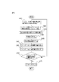
- FIG. 8 is a flow chart showing the operation flow of the temperature estimation device according to the third embodiment of the present disclosure.
- the temperature estimation process of the power semiconductor element in the temperature estimation device 1 according to the third embodiment of the present disclosure and the converter system 100 including the same is performed when the converter system 100 is connected to the three-phase AC power supply 4 and actually operated. cyclically.
- step S301 the voltage detection unit 13 detects the value of the inter-terminal voltage of the converter 2 on the three-phase AC power supply 4 side.
- the ambient temperature detection unit 14 detects the ambient temperature of the power semiconductor element based on the signal sent from the temperature detection element 35 .
- the current detection unit 11 detects the value of the current flowing through the power semiconductor elements provided in the three-phase bridge circuit 31 of the converter 2 (the value of the current input to the converter 2).
- step S303 the current comparator 25 compares the current value detected by the current detector 11 with a predetermined current threshold. If it is determined in step S303 that the value of the current detected by the current detection unit 11 is equal to or greater than the current threshold, the process proceeds to step S304. If so, the process proceeds to step S309.
- step S ⁇ b>304 the unbalance rate calculator 21 calculates the unbalance rate of the three-phase AC power supply 4 .
- the unbalance rate of the three-phase AC power supply 4 to be calculated may be a voltage unbalance rate or a current unbalance rate.
- step S305 the unbalance rate comparison unit 26 compares the unbalance rate calculated by the unbalance rate calculation unit 21 with a predetermined unbalance rate threshold. If it is determined in step S305 that the unbalanced rate calculated by the unbalanced rate calculator 21 is equal to or greater than the unbalanced rate threshold, the process proceeds to step S306, where the unbalanced rate calculated by the unbalanced rate calculator 21 is If it is determined that the imbalance rate is less than the threshold, the process proceeds to step S309.
- step S306 the temperature compensation coefficient calculation unit 22 uses the unbalance rate calculated by the unbalance rate calculation unit 21 to calculate the temperature compensation coefficient.
- step S ⁇ b>307 the provisional value calculation unit 23 calculates the value based on the value of the current detected by the current detection unit 11 , the value of the resistance component of the power semiconductor element, and the ambient temperature of the power semiconductor element detected by the ambient temperature detection unit 14 . to calculate a provisional junction temperature value of the power semiconductor element.
- step S308 the estimated value calculation unit 24 multiplies the junction temperature provisional value calculated by the provisional value calculation unit 23 by the temperature compensation coefficient calculated by the temperature compensation coefficient calculation unit 22, and calculates the power semiconductor Output as the junction temperature estimate of the device.
- step S303 determines whether the value of the current detected by the current detection unit 11 is less than the current threshold, or if the unbalance rate calculated by the unbalance rate calculation unit 21 in step S305 is less than the unbalance rate threshold .
- step S309 the provisional value calculation unit 23 calculates the current value detected by the current detection unit 11, the terminal voltage value detected by the voltage detection unit 13, and the ambient temperature detection unit A provisional junction temperature value of the power semiconductor element is calculated based on the ambient temperature of the power semiconductor element detected by 14 .
- step S310 the estimated value calculator 24 outputs the junction temperature provisional value calculated by the provisional value calculator 23 as the junction temperature estimated value of the power semiconductor element.
- junction temperature estimated values calculated by the estimated value calculator 24 in steps S308 and S310 are sent to the temperature comparator 15 .
- the junction temperature estimated value calculated by the estimated value calculator 24 may be displayed on, for example, a display unit (not shown), or may be output by sound from an acoustic device (not shown).
- step S311 the temperature comparator 15 compares the junction temperature estimated value calculated by the estimated value calculator 24 in the junction temperature estimator 12 with a predetermined temperature threshold. If it is determined in step S311 that the estimated junction temperature is equal to or higher than the temperature threshold, the process proceeds to step S312, and if it is determined that the estimated junction temperature is less than the temperature threshold, the process returns to step S301.
- step S312 the alarm output unit 16 outputs an alarm.
- steps S301 to S312 described above are periodically and repeatedly executed until an alarm is output by the alarm output unit 16 in step S311.
- the unbalance rate calculation unit 21 and the temperature compensation coefficient calculation unit 22 do not operate. Calculation load of the arithmetic processing unit constituting the unbalance rate calculation unit 21 and the temperature compensation coefficient calculation unit 22 is reduced. Therefore, compared to the first embodiment, the third embodiment of the present disclosure reduces the ratio of the junction temperature estimation process (for example, the CPU usage rate) in the arithmetic processing of the arithmetic processing unit, while reducing the accuracy of the junction temperature estimated value.
- the junction temperature estimation process for example, the CPU usage rate
- step S305 If it is determined in step S305 that the unbalanced rate calculated by the unbalanced rate calculator 21 is less than the unbalanced rate threshold value, the temperature compensation coefficient calculator 22 does not operate, and the temperature compensation coefficient calculator 22 is The calculation load of the constituent arithmetic processing unit is reduced. Therefore, compared to the second embodiment, the third embodiment of the present disclosure reduces the ratio of the junction temperature estimation process (for example, the CPU usage rate) in the arithmetic processing of the arithmetic processing unit, while reducing the accuracy of the junction temperature estimated value. can increase
- the fourth embodiment of the present disclosure detects the value of the current flowing through the power semiconductor element for each phase of the converter, and calculates the junction temperature estimation value of the power semiconductor element through which the maximum current flows.
- connection relationship of each element in the temperature estimating device and the converter system including the same according to the fourth embodiment of the present disclosure is the connection of each element in the temperature estimating device and the converter system including the same according to the first embodiment shown in FIG. Same as relationship.
- each operation of the provisional value calculation unit 23 and the estimated value calculation unit 24 in the current detection unit 11 and the junction temperature estimation unit 12 according to the fourth embodiment of the present disclosure is the same as that of the current detection unit 11 and the current detection unit 24 according to the first embodiment.
- the operations of the provisional value calculator 23 and the estimated value calculator 24 in the junction temperature estimator 12 are different. Specifically, it is as follows.
- the current detection unit 11 detects the value of the current flowing through the power semiconductor elements of the three-phase bridge circuit 31 of the converter 2 for each phase of the converter. That is, the current detection unit 11 detects the value of the current flowing through the R-phase power semiconductor element, the value of the current flowing through the S-phase power semiconductor element, and the current flowing through the T-phase power semiconductor element of the three-phase bridge circuit 31. Detect value. The current value of each phase detected by the current detector 11 is sent to the provisional value calculator 23 .
- the junction temperature estimating unit 12 estimates the maximum current value based on the junction temperature provisional value calculated based at least on the maximum value among the current values of the respective phases detected by the current detecting unit 11 and the unbalance rate. Calculates the junction temperature estimation value of the power semiconductor element through which the current flows.
- the operations of the provisional value calculator 23 and the estimated value calculator 24 in the junction temperature estimator 12 are described in more detail below.
- the provisional value calculator 23 identifies the maximum current value among the phase currents detected by the current detector 11, and compares the maximum current value and the current detected by the voltage detector 13. Based on the value of the inter-terminal voltage and the ambient temperature of the power semiconductor element detected by the ambient temperature detection unit 14, a provisional junction temperature value of the power semiconductor element through which the maximum current flows is calculated.
- the estimated value calculator 24 multiplies the provisional value of the junction temperature of the power semiconductor element through which the maximum current calculated by the provisional value calculation unit 23 flows by the temperature compensation coefficient calculated by the temperature compensation coefficient calculation unit 22. The obtained value is output as the junction temperature estimation value of the power semiconductor element through which the maximum current flows.
- thermoestimating device 1 In the temperature estimating device 1 according to the fourth embodiment of the present disclosure and the converter system 100 including the same, configurations and operations other than the current detecting unit 11 and the provisional value calculating unit 23 and the estimated value calculating unit 24 in the junction temperature estimating unit 12 is the same as the configuration and operation described with reference to FIG. 1, so description thereof will be omitted.
- FIG. 9 is a flow chart showing the operation flow of the temperature estimation device according to the fourth embodiment of the present disclosure.
- the temperature estimation process of the power semiconductor element in the temperature estimation device 1 and the converter system 100 including the temperature estimation device 1 according to the fourth embodiment of the present disclosure is performed when the converter system 100 is connected to the three-phase AC power supply 4 and actually operated. cyclically.
- step S401 the voltage detection unit 13 detects the value of the inter-terminal voltage of the converter 2 on the three-phase AC power supply 4 side.
- the ambient temperature detection unit 14 detects the ambient temperature of the power semiconductor element based on the signal sent from the temperature detection element 35 .
- step S402 the current detection unit 11 detects the value of the current flowing through the power semiconductor element of the three-phase bridge circuit 31 of the converter 2 (the value of the current of each phase input to the converter 2) as described above. Detect for each phase of the converter. The current value of each phase detected by the current detector 11 is sent to the provisional value calculator 23 .
- step S403 the provisional value calculator 23 identifies the maximum current value among the phase currents detected by the current detector 11 .
- step S404 the unbalance rate calculator 21 calculates the unbalance rate of the three-phase AC power supply 4.
- the unbalance rate of the three-phase AC power supply 4 to be calculated may be a voltage unbalance rate or a current unbalance rate.
- step S405 the temperature compensation coefficient calculation unit 22 uses the unbalance rate calculated by the unbalance rate calculation unit 21 to calculate the temperature compensation coefficient.
- step S403 The order of the processing in step S403 and the processing in steps S404 and S405 may be changed.
- step S ⁇ b>406 the provisional value calculation unit 23 calculates the maximum current value specified in step S ⁇ b>403 , the value of the resistance component of the power semiconductor element, and the ambient temperature of the power semiconductor element detected by the ambient temperature detection unit 14 . Based on this, the provisional junction temperature value of the power semiconductor element through which the current having the maximum value flows is calculated.
- the estimated value calculation unit 24 calculates the junction temperature provisional value of the power semiconductor element through which the maximum current calculated by the provisional value calculation unit 23 flows, and the temperature compensation coefficient calculated by the temperature compensation coefficient calculation unit 22. A value obtained by multiplying is output as an estimated junction temperature value of the power semiconductor device through which the current having the maximum value flows.
- the junction temperature estimated value calculated by the estimated value calculator 24 in step S ⁇ b>407 is sent to the temperature comparator 15 .
- the junction temperature estimated value calculated by the estimated value calculator 24 may be displayed on, for example, a display unit (not shown), or may be output by sound from an acoustic device (not shown).
- step S408 the temperature comparator 15 compares the junction temperature estimated value calculated by the estimated value calculator 24 in the junction temperature estimator 12 with a predetermined temperature threshold. If it is determined in step S408 that the estimated junction temperature is greater than or equal to the temperature threshold, the process proceeds to step S409, and if it is determined that the estimated junction temperature is less than the temperature threshold, the process returns to step S401.
- step S409 the alarm output unit 16 outputs an alarm.
- steps S401 to S409 described above are periodically and repeatedly executed until an alarm is output by the alarm output unit 16 in step S408.
- the power semiconductor element provided in the phase through which the maximum current flows has the greatest heat generation, and is highly likely to be damaged and shortened in life.
- whether or not to output an alarm is determined based on the estimated junction temperature of the power semiconductor device through which the maximum current flows, so the power semiconductor device is more reliably protected from overheating. It is possible to reduce the possibility of damage and shortening of the life of the power semiconductor element.
- An arithmetic processing device is provided in the temperature estimation device 1 according to the first to fourth embodiments.
- This arithmetic processing unit has the current detection unit 11, the junction temperature estimation unit 12, the voltage detection unit 13, the ambient temperature detection unit 14, the temperature comparison unit 15, and the alarm output unit 16 described above.
- Each of these units of the arithmetic processing unit is, for example, a functional module realized by a computer program executed on the processor.
- the arithmetic processing unit is By operating according to the program, the function of each part can be realized.
- a computer program for executing each process of the current detection unit 11, the junction temperature estimation unit 12, the voltage detection unit 13, the ambient temperature detection unit 14, the temperature comparison unit 15, and the alarm output unit 16 includes a semiconductor memory and a magnetic recording medium. Alternatively, it may be provided in a form recorded on a computer-readable recording medium such as an optical recording medium.
- the current detection unit 11, the junction temperature estimation unit 12, the voltage detection unit 13, the ambient temperature detection unit 14, the temperature comparison unit 15, and the alarm output unit 16 are implemented by a semiconductor integrated circuit in which a computer program for realizing the functions of each unit is written. It may be realized as a circuit.
Landscapes
- Engineering & Computer Science (AREA)
- Power Engineering (AREA)
- Physics & Mathematics (AREA)
- General Physics & Mathematics (AREA)
- Power Conversion In General (AREA)
- Inverter Devices (AREA)
- Rectifiers (AREA)
Abstract
Description

















2 コンバータ
3 コンバータ制御装置
4 三相交流電源
5 インバータ
6 モータ
11 電流検出部
12 ジャンクション温度推定部
13 電圧検出部
14 周囲温度検出部
15 温度比較部
16 アラーム出力部
21 不平衡率算出部
22 温度補償係数算出部
23 暫定値算出部
24 推定値算出部
25 電流比較部
26 不平衡率比較部
31 三相ブリッジ回路
32 平滑コンデンサ
33 DCリンクコンデンサ
34 予備充電回路
35 温度検出素子
41 スイッチング制御部
42 DCリンク部電圧検出部
Claims (11)
- 三相交流電源側の交流電力と直流側における直流電力との間で電力変換を行うコンバータに設けられたパワー半導体素子のジャンクション温度推定値を算出する温度推定装置であって、
前記パワー半導体素子に流れる電流の値を検出する電流検出部と、
前記電流検出部により検出された前記電流の値に少なくとも基づいて算出したジャンクション温度暫定値と前記コンバータに接続される前記三相交流電源の不平衡率とに基づいて、前記パワー半導体素子のジャンクション温度推定値を算出するジャンクション温度推定部と、
を備える、温度推定装置。 - 前記ジャンクション温度推定部は、
前記不平衡率を算出する不平衡率算出部と、
前記不平衡率に基づいて温度補償係数を算出する温度補償係数算出部と、
前記ジャンクション温度暫定値を算出する暫定値算出部と、
前記ジャンクション温度暫定値と前記温度補償係数とを乗算して得られる値を、前記ジャンクション温度推定値として出力する推定値算出部と、
を有する、請求項1に記載の温度推定装置。 - 前記暫定値算出部は、前記電流検出部により検出された前記電流の値と前記パワー半導体素子の抵抗成分の値とに少なくとも基づいて、前記ジャンクション温度暫定値を算出する、請求項2に記載の温度推定装置。
- 前記パワー半導体素子の周囲温度を検出する周囲温度検出部をさらに備え、
前記暫定値算出部は、前記電流検出部により検出された前記電流の値と前記周囲温度とに少なくとも基づいて、前記ジャンクション温度暫定値を算出する、請求項2または3に記載の温度推定装置。 - 前記コンバータの三相交流電源側の端子間電圧の値を検出する電圧検出部をさらに備え、
前記不平衡率算出部は、前記電圧検出部によって検出された前記端子間電圧の値に基づいて前記不平衡率を算出する、請求項2に記載の温度推定装置。 - 前記不平衡率算出部は、前記電流検出部によって検出された前記電流の値に基づいて前記不平衡率を算出する、請求項2に記載の温度推定装置。
- 前記ジャンクション温度推定部は、前記電流検出部によって検出された前記電流の値と所定の電流閾値とを比較する電流比較部をさらに有し、
前記推定値算出部は、前記電流検出部により検出された前記電流の値が前記電流閾値以上である場合は、前記ジャンクション温度暫定値と前記温度補償係数とを乗算して得られる値を前記ジャンクション温度推定値として出力し、前記電流検出部により検出された前記電流の値が前記電流閾値未満である場合は、前記ジャンクション温度暫定値を前記ジャンクション温度推定値として出力する、請求項2~6のいずれか一項に記載の温度推定装置。 - 前記ジャンクション温度推定部は、前記電流検出部によって検出された前記電流の値と所定の電流閾値とを比較する電流比較部と、前記不平衡率と所定の不平衡率閾値とを比較する不平衡率電流比較部と、をさらに有し、
前記推定値算出部は、前記電流検出部により検出された前記電流の値が前記電流閾値以上かつ前記不平衡率が前記不平衡率閾値以上である場合は、前記ジャンクション温度暫定値と前記温度補償係数とを乗算して得られる値を前記ジャンクション温度推定値として出力し、前記電流検出部により検出された前記電流の値が前記電流閾値未満である場合または前記電流検出部により検出された前記電流の値が前記電流閾値以上かつ前記不平衡率が前記不平衡率閾値未満である場合は、前記ジャンクション温度暫定値を前記ジャンクション温度推定値として出力する、請求項2~6のいずれか一項に記載の温度推定装置。 - 前記電流検出部は、前記パワー半導体素子に流れる電流の値を、前記コンバータの各相ごとに検出し、
前記ジャンクション温度推定部は、前記電流検出部により検出された各相の前記電流の値のうちの最大値に少なくとも基づいて算出したジャンクション温度暫定値と前記不平衡率とに基づいて、前記最大値となる電流が流れる前記パワー半導体素子のジャンクション温度推定値を算出する、請求項1~8のいずれか一項に記載の温度推定装置。 - 前記ジャンクション温度推定部により算出された前記ジャンクション温度推定値と所定の温度閾値とを比較する温度比較部と、
前記ジャンクション温度推定値が前記温度閾値以上である場合、アラームを出力するアラーム出力部と、
をさらに備える、請求項1~9のいずれか一項に記載の温度推定装置。 - 請求項1~9のいずれか一項に記載の温度推定装置と、
前記パワー半導体素子が設けられ、前記パワー半導体素子がオンオフ動作することにより三相交流電源側の交流電力と直流側における直流電力との間で電力変換を行う前記コンバータと、
を備え、
前記ジャンクション温度推定部は、前記パワー半導体素子のジャンクション温度推定値を算出する、コンバータシステム。
Priority Applications (5)
| Application Number | Priority Date | Filing Date | Title |
|---|---|---|---|
| JP2023522102A JP7564356B2 (ja) | 2021-05-19 | 2021-05-19 | 温度推定装置及びコンバータシステム |
| US18/289,270 US20240255356A1 (en) | 2021-05-19 | 2021-05-19 | Temperature inference device and converter system |
| CN202180098066.7A CN117280592A (zh) | 2021-05-19 | 2021-05-19 | 温度估计装置和转换器系统 |
| DE112021007283.8T DE112021007283T5 (de) | 2021-05-19 | 2021-05-19 | Temperaturinferenzvorrichtung und wandlersystem |
| PCT/JP2021/019067 WO2022244166A1 (ja) | 2021-05-19 | 2021-05-19 | 温度推定装置及びコンバータシステム |
Applications Claiming Priority (1)
| Application Number | Priority Date | Filing Date | Title |
|---|---|---|---|
| PCT/JP2021/019067 WO2022244166A1 (ja) | 2021-05-19 | 2021-05-19 | 温度推定装置及びコンバータシステム |
Publications (1)
| Publication Number | Publication Date |
|---|---|
| WO2022244166A1 true WO2022244166A1 (ja) | 2022-11-24 |
Family
ID=84140177
Family Applications (1)
| Application Number | Title | Priority Date | Filing Date |
|---|---|---|---|
| PCT/JP2021/019067 Ceased WO2022244166A1 (ja) | 2021-05-19 | 2021-05-19 | 温度推定装置及びコンバータシステム |
Country Status (5)
| Country | Link |
|---|---|
| US (1) | US20240255356A1 (ja) |
| JP (1) | JP7564356B2 (ja) |
| CN (1) | CN117280592A (ja) |
| DE (1) | DE112021007283T5 (ja) |
| WO (1) | WO2022244166A1 (ja) |
Families Citing this family (3)
| Publication number | Priority date | Publication date | Assignee | Title |
|---|---|---|---|---|
| DE112021003307T5 (de) * | 2020-08-25 | 2023-04-20 | Sanden Corporation | Wechselrichtervorrichtung und damit ausgerüsteter elektrischer kompressor für fahrzeuge |
| EP4489277A4 (en) * | 2023-05-17 | 2025-09-03 | Huawei Digital Power Tech Co Ltd | POWER CONVERTER AND METHOD FOR DETERMINING AN ABNORMAL TERMINAL OF A POWER CONVERTER |
| CN119891724B (zh) * | 2024-12-27 | 2026-01-09 | 青岛海信网络能源股份有限公司 | 变流设备及变流设备的控制方法 |
Citations (2)
| Publication number | Priority date | Publication date | Assignee | Title |
|---|---|---|---|---|
| JP2013201870A (ja) * | 2012-03-26 | 2013-10-03 | Mitsubishi Electric Corp | 電力変換器 |
| WO2016170584A1 (ja) * | 2015-04-20 | 2016-10-27 | 三菱電機株式会社 | 電力変換装置 |
Family Cites Families (6)
| Publication number | Priority date | Publication date | Assignee | Title |
|---|---|---|---|---|
| JP2008131722A (ja) | 2006-11-20 | 2008-06-05 | Nippon Reliance Kk | パワー素子過熱保護装置 |
| JP2009261078A (ja) | 2008-04-15 | 2009-11-05 | Yaskawa Electric Corp | モータ制御装置と温度推定方法 |
| US9030174B2 (en) * | 2012-09-14 | 2015-05-12 | General Electric Company | Current balance control in converter for doubly fed induction generator wind turbine system |
| CN109526244A (zh) * | 2016-07-21 | 2019-03-26 | 日本电产株式会社 | 马达模块、马达控制装置、温度估计装置以及温度估计方法 |
| US10090792B2 (en) * | 2016-12-08 | 2018-10-02 | Ford Global Technologies, Llc | Self-balancing parallel power devices with a temperature compensated gate driver |
| US10615727B2 (en) * | 2018-08-27 | 2020-04-07 | General Electric Company | Dynamic brake circuit assembly for a wind turbine |
-
2021
- 2021-05-19 WO PCT/JP2021/019067 patent/WO2022244166A1/ja not_active Ceased
- 2021-05-19 US US18/289,270 patent/US20240255356A1/en not_active Abandoned
- 2021-05-19 JP JP2023522102A patent/JP7564356B2/ja active Active
- 2021-05-19 DE DE112021007283.8T patent/DE112021007283T5/de active Pending
- 2021-05-19 CN CN202180098066.7A patent/CN117280592A/zh active Pending
Patent Citations (2)
| Publication number | Priority date | Publication date | Assignee | Title |
|---|---|---|---|---|
| JP2013201870A (ja) * | 2012-03-26 | 2013-10-03 | Mitsubishi Electric Corp | 電力変換器 |
| WO2016170584A1 (ja) * | 2015-04-20 | 2016-10-27 | 三菱電機株式会社 | 電力変換装置 |
Also Published As
| Publication number | Publication date |
|---|---|
| JP7564356B2 (ja) | 2024-10-08 |
| DE112021007283T5 (de) | 2024-01-11 |
| US20240255356A1 (en) | 2024-08-01 |
| CN117280592A (zh) | 2023-12-22 |
| JPWO2022244166A1 (ja) | 2022-11-24 |
Similar Documents
| Publication | Publication Date | Title |
|---|---|---|
| CN110829944B (zh) | 电动机驱动装置 | |
| CN112909895B (zh) | 马达驱动装置 | |
| CN104736981B (zh) | 半导体芯片温度推定装置及过热保护装置 | |
| CN102124639B (zh) | 三相逆变器的电源电路保护装置 | |
| CN115485945B (zh) | 检测并联驱动的开关的故障的故障检测装置及电动机驱动装置 | |
| JP7564356B2 (ja) | 温度推定装置及びコンバータシステム | |
| JP7620090B2 (ja) | コンデンサ劣化検出装置及びコンバータシステム | |
| CN104113258A (zh) | 具备dc连接部异常检测功能的电动机驱动装置 | |
| JP2012120376A (ja) | インバータ装置 | |
| JP6616437B2 (ja) | Dcリンク部のコンデンサの短絡判定部を有するモータ駆動装置 | |
| CN112994583B (zh) | 马达驱动装置 | |
| WO2022264314A1 (ja) | モータの絶縁抵抗値を計算するモータ駆動装置 | |
| WO2022264315A1 (ja) | モータの絶縁抵抗値を計算するモータ駆動装置 | |
| US20230143105A1 (en) | Motor drive device that calculates insulation resistance value of motor | |
| JP7324140B2 (ja) | 予備充電回路を有するモータ駆動装置 | |
| JP2019138656A (ja) | Dcリンク部のコンデンサの短絡判定部を有するモータ駆動装置 | |
| JP6344558B2 (ja) | 半導体電力変換器の故障検出装置 | |
| JP2001086764A (ja) | インバータ | |
| JP2020092553A (ja) | 予備充電回路を有するモータ駆動装置 | |
| JP7372207B2 (ja) | リアクトルの層間短絡を検出するコンバータ装置 | |
| WO2023233477A1 (ja) | 交流入力電源の遮断状態を検知するモータ駆動装置 | |
| WO2026033723A1 (ja) | 回生動作中の停電を検出するモータ駆動装置 | |
| JP2019140717A (ja) | Dcリンク部のコンデンサの短絡判定部を有するモータ駆動装置 |
Legal Events
| Date | Code | Title | Description |
|---|---|---|---|
| 121 | Ep: the epo has been informed by wipo that ep was designated in this application |
Ref document number: 21940780 Country of ref document: EP Kind code of ref document: A1 |
|
| WWE | Wipo information: entry into national phase |
Ref document number: 2023522102 Country of ref document: JP |
|
| WWE | Wipo information: entry into national phase |
Ref document number: 18289270 Country of ref document: US |
|
| WWE | Wipo information: entry into national phase |
Ref document number: 202180098066.7 Country of ref document: CN |
|
| WWE | Wipo information: entry into national phase |
Ref document number: 112021007283 Country of ref document: DE |
|
| 122 | Ep: pct application non-entry in european phase |
Ref document number: 21940780 Country of ref document: EP Kind code of ref document: A1 |