WO2022230847A1 - 照明光学系、露光装置及びフラットパネルディスプレイの製造方法 - Google Patents
照明光学系、露光装置及びフラットパネルディスプレイの製造方法 Download PDFInfo
- Publication number
- WO2022230847A1 WO2022230847A1 PCT/JP2022/018810 JP2022018810W WO2022230847A1 WO 2022230847 A1 WO2022230847 A1 WO 2022230847A1 JP 2022018810 W JP2022018810 W JP 2022018810W WO 2022230847 A1 WO2022230847 A1 WO 2022230847A1
- Authority
- WO
- WIPO (PCT)
- Prior art keywords
- light
- pulsed light
- pulsed
- optical system
- illumination
- Prior art date
- Legal status (The legal status is an assumption and is not a legal conclusion. Google has not performed a legal analysis and makes no representation as to the accuracy of the status listed.)
- Ceased
Links
Images












Classifications
-
- G—PHYSICS
- G03—PHOTOGRAPHY; CINEMATOGRAPHY; ANALOGOUS TECHNIQUES USING WAVES OTHER THAN OPTICAL WAVES; ELECTROGRAPHY; HOLOGRAPHY
- G03F—PHOTOMECHANICAL PRODUCTION OF TEXTURED OR PATTERNED SURFACES, e.g. FOR PRINTING, FOR PROCESSING OF SEMICONDUCTOR DEVICES; MATERIALS THEREFOR; ORIGINALS THEREFOR; APPARATUS SPECIALLY ADAPTED THEREFOR
- G03F7/00—Photomechanical, e.g. photolithographic, production of textured or patterned surfaces, e.g. printing surfaces; Materials therefor, e.g. comprising photoresists; Apparatus specially adapted therefor
- G03F7/20—Exposure; Apparatus therefor
-
- G—PHYSICS
- G03—PHOTOGRAPHY; CINEMATOGRAPHY; ANALOGOUS TECHNIQUES USING WAVES OTHER THAN OPTICAL WAVES; ELECTROGRAPHY; HOLOGRAPHY
- G03F—PHOTOMECHANICAL PRODUCTION OF TEXTURED OR PATTERNED SURFACES, e.g. FOR PRINTING, FOR PROCESSING OF SEMICONDUCTOR DEVICES; MATERIALS THEREFOR; ORIGINALS THEREFOR; APPARATUS SPECIALLY ADAPTED THEREFOR
- G03F7/00—Photomechanical, e.g. photolithographic, production of textured or patterned surfaces, e.g. printing surfaces; Materials therefor, e.g. comprising photoresists; Apparatus specially adapted therefor
- G03F7/70—Microphotolithographic exposure; Apparatus therefor
- G03F7/70058—Mask illumination systems
- G03F7/70208—Multiple illumination paths, e.g. radiation distribution devices, microlens illumination systems, multiplexers or demultiplexers for single or multiple projection systems
-
- G—PHYSICS
- G02—OPTICS
- G02B—OPTICAL ELEMENTS, SYSTEMS OR APPARATUS
- G02B26/00—Optical devices or arrangements for the control of light using movable or deformable optical elements
- G02B26/08—Optical devices or arrangements for the control of light using movable or deformable optical elements for controlling the direction of light
- G02B26/10—Scanning systems
-
- G—PHYSICS
- G02—OPTICS
- G02B—OPTICAL ELEMENTS, SYSTEMS OR APPARATUS
- G02B6/00—Light guides; Structural details of arrangements comprising light guides and other optical elements, e.g. couplings
- G02B6/24—Coupling light guides
- G02B6/26—Optical coupling means
- G02B6/35—Optical coupling means having switching means
- G02B6/351—Optical coupling means having switching means involving stationary waveguides with moving interposed optical elements
- G02B6/3512—Optical coupling means having switching means involving stationary waveguides with moving interposed optical elements the optical element being reflective, e.g. mirror
-
- G—PHYSICS
- G03—PHOTOGRAPHY; CINEMATOGRAPHY; ANALOGOUS TECHNIQUES USING WAVES OTHER THAN OPTICAL WAVES; ELECTROGRAPHY; HOLOGRAPHY
- G03F—PHOTOMECHANICAL PRODUCTION OF TEXTURED OR PATTERNED SURFACES, e.g. FOR PRINTING, FOR PROCESSING OF SEMICONDUCTOR DEVICES; MATERIALS THEREFOR; ORIGINALS THEREFOR; APPARATUS SPECIALLY ADAPTED THEREFOR
- G03F7/00—Photomechanical, e.g. photolithographic, production of textured or patterned surfaces, e.g. printing surfaces; Materials therefor, e.g. comprising photoresists; Apparatus specially adapted therefor
- G03F7/70—Microphotolithographic exposure; Apparatus therefor
- G03F7/70008—Production of exposure light, i.e. light sources
- G03F7/70025—Production of exposure light, i.e. light sources by lasers
-
- G—PHYSICS
- G03—PHOTOGRAPHY; CINEMATOGRAPHY; ANALOGOUS TECHNIQUES USING WAVES OTHER THAN OPTICAL WAVES; ELECTROGRAPHY; HOLOGRAPHY
- G03F—PHOTOMECHANICAL PRODUCTION OF TEXTURED OR PATTERNED SURFACES, e.g. FOR PRINTING, FOR PROCESSING OF SEMICONDUCTOR DEVICES; MATERIALS THEREFOR; ORIGINALS THEREFOR; APPARATUS SPECIALLY ADAPTED THEREFOR
- G03F7/00—Photomechanical, e.g. photolithographic, production of textured or patterned surfaces, e.g. printing surfaces; Materials therefor, e.g. comprising photoresists; Apparatus specially adapted therefor
- G03F7/70—Microphotolithographic exposure; Apparatus therefor
- G03F7/70008—Production of exposure light, i.e. light sources
- G03F7/7005—Production of exposure light, i.e. light sources by multiple sources, e.g. light-emitting diodes [LED] or light source arrays
-
- G—PHYSICS
- G03—PHOTOGRAPHY; CINEMATOGRAPHY; ANALOGOUS TECHNIQUES USING WAVES OTHER THAN OPTICAL WAVES; ELECTROGRAPHY; HOLOGRAPHY
- G03F—PHOTOMECHANICAL PRODUCTION OF TEXTURED OR PATTERNED SURFACES, e.g. FOR PRINTING, FOR PROCESSING OF SEMICONDUCTOR DEVICES; MATERIALS THEREFOR; ORIGINALS THEREFOR; APPARATUS SPECIALLY ADAPTED THEREFOR
- G03F7/00—Photomechanical, e.g. photolithographic, production of textured or patterned surfaces, e.g. printing surfaces; Materials therefor, e.g. comprising photoresists; Apparatus specially adapted therefor
- G03F7/70—Microphotolithographic exposure; Apparatus therefor
- G03F7/70058—Mask illumination systems
- G03F7/7015—Details of optical elements
-
- G—PHYSICS
- G03—PHOTOGRAPHY; CINEMATOGRAPHY; ANALOGOUS TECHNIQUES USING WAVES OTHER THAN OPTICAL WAVES; ELECTROGRAPHY; HOLOGRAPHY
- G03F—PHOTOMECHANICAL PRODUCTION OF TEXTURED OR PATTERNED SURFACES, e.g. FOR PRINTING, FOR PROCESSING OF SEMICONDUCTOR DEVICES; MATERIALS THEREFOR; ORIGINALS THEREFOR; APPARATUS SPECIALLY ADAPTED THEREFOR
- G03F7/00—Photomechanical, e.g. photolithographic, production of textured or patterned surfaces, e.g. printing surfaces; Materials therefor, e.g. comprising photoresists; Apparatus specially adapted therefor
- G03F7/70—Microphotolithographic exposure; Apparatus therefor
- G03F7/70216—Mask projection systems
- G03F7/70283—Mask effects on the imaging process
- G03F7/70291—Addressable masks, e.g. spatial light modulators [SLMs], digital micro-mirror devices [DMDs] or liquid crystal display [LCD] patterning devices
Definitions
- the present invention relates to an illumination optical system, an exposure apparatus, and a method of manufacturing a flat panel display.
- This application is based on Japanese Patent Application No. 2021-075408 filed on April 27, 2021, Japanese Patent Application No. 2021-075409 filed on April 27, 2021 and filed on April 27, 2021.
- the priority is claimed based on Japanese Patent Application No. 2021-075410, the contents of which are incorporated herein.
- steppers step-and-repeat type projection exposure apparatuses
- steppers step-and-repeat type projection exposure apparatuses
- steppers step-and-repeat type projection exposure apparatuses
- steppers step-and-repeat type projection exposure apparatuses
- steppers step-and-repeat type projection exposure apparatuses
- steppers step-and-repeat type projection exposure apparatuses
- steppers step-and-repeat type projection exposure apparatuses
- a substrate such as a glass plate coated with a photosensitive agent on its surface or a wafer (hereinafter collectively referred to as substrate) is placed on a substrate stage device as an object to be exposed. Then, by irradiating a pulsed light onto the spatial light modulating element on which the circuit pattern is formed, and irradiating the substrate with the pulsed light that has passed through the spatial light modulating element through an optical system such as a projection lens, the circuit pattern is formed on the substrate. It is transferred to the top (see, for example, Patent Document 1).
- a plurality of light sources emitting pulsed light, and the pulsed light emitted from each of the plurality of light sources are a splitting unit for splitting into a first pulsed light and a second pulsed light; a delay optical system for guiding the second pulsed light to a second optical path longer than a first optical path through which the first pulsed light travels; and the first pulse.
- an optical system comprising: a synthesizing/splitting unit that synthesizes the light and the second pulsed light that has passed through the delay optical system, and splits and outputs the synthesized pulsed light; and the pulse emitted from the optical system.
- an illumination system for directing each of the lights onto the mask and illuminating the mask.
- the exposure target is divided by irradiating the exposure target with light emitted from the illumination optical system, the illumination optical system, and the mask illuminated by the pulsed light.
- An exposure apparatus is provided that includes a projection optical system for exposure and a stage on which an exposure target can be placed.
- a method of manufacturing a flat panel display including exposing an exposure target using the exposure apparatus described above and developing the exposed exposure target. .
- the first light source emits a first pulsed light at a first time.
- a second light source emitting a second pulsed light at a second time different from the first time, and guiding the first and second pulsed lights respectively to the spatial light modulator to illuminate the spatial light modulator.
- an illumination optical system wherein the second light source emits the second pulsed light at the second time when the time interval from the first time is shorter than the predetermined time interval.
- the substrate by irradiating the substrate with light emitted from the above-described illumination optical system and the plurality of spatial light modulators illuminated by the first and second pulsed lights, respectively, , and a projection optical system for performing divisional exposure on the substrate.
- a method for manufacturing a flat panel display including exposing a substrate for a flat panel display using the exposure apparatus described above and developing the exposed substrate. provided.
- the first light source emits the first pulsed light at the first time.
- a second light source emitting a second pulsed light at a second time interval shorter than the predetermined time interval from the first time interval and different from the first time interval; and , respectively directing the first and second pulsed lights to the spatial light modulator to illuminate the spatial light modulator.
- device fabrication comprising exposing onto a substrate an image of the spatial light modulator illuminated by the illumination method described above, and developing the exposed substrate. A method is provided.
- a flat panel comprising: exposing onto a substrate an image of said spatial light modulator illuminated by the illumination method described above; and developing said exposed substrate.
- a method of manufacturing a display is provided.
- the illumination optical system for illuminating a mask on which a predetermined pattern is formed a splitting unit for splitting; a delay optical system for guiding the second pulsed light to a second optical path longer than the first optical path along which the first pulsed light passes; a synthesizing unit that synthesizes two pulsed lights; and an illumination system that guides the first and second pulsed lights synthesized by the synthesizing unit to the mask and illuminates the mask
- the delay optical system includes a reflecting section that reflects the second pulsed light, and an optical member that causes the reflected second pulsed light to enter the reflecting section again.
- the above-described illumination optical system and a projection optical system for dividing and exposing an exposure target by irradiating the exposure target with light emitted from the mask illuminated by the pulsed light. and a stage on which an exposure target can be placed.
- a method of manufacturing a flat panel display including exposing an exposure target using the exposure apparatus described above and developing the exposed exposure target. .
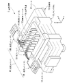
- FIG. 1 is a diagram showing an overview of the external configuration of an exposure apparatus 1 of this embodiment.
- the exposure apparatus 1 is an apparatus that irradiates an exposure target with modulated light.
- the exposure apparatus 1 is a step-and-scan projection exposure apparatus, a so-called scanner, which exposes a rectangular (square) glass substrate used in a liquid crystal display (flat panel display) or the like. is.
- the glass substrate which is the object to be exposed, has at least one side length or diagonal length of 500 mm or more, and may be a substrate for a flat panel display.
- An exposure target (for example, a substrate for a flat panel display) exposed by the exposure apparatus 1 is developed and provided as a product.
- the apparatus main body of the exposure apparatus 1 is configured similarly to the apparatus main body disclosed in US Patent Application Publication No. 2008/0030702, for example.
- the exposure apparatus 1 includes a base 11, an anti-vibration table 12, a main column 13, a stage 14, an optical surface plate 15, an illumination module 16, a projection module 17, a light source unit 18, an optical fiber 19, and an optical modulator 20 (not shown).
- the direction parallel to the optical axis direction of the projection module 17 that irradiates the light modulated by the light modulation section 20 onto the exposure object is defined as the Z-axis direction
- the direction of a predetermined plane orthogonal to the Z-axis is defined as the X-axis direction
- the X-axis direction and the Y-axis direction are directions orthogonal (intersecting) each other.
- the base 11 is the base of the exposure apparatus 1 and is installed on the anti-vibration table 12 .
- the base 11 supports a stage 14 on which an object to be exposed is placed so as to be movable in the X-axis direction and the Y-axis direction.
- the stage 14 supports the exposure object and positions the exposure object with high precision with respect to a plurality of partial images of the circuit pattern projected via the projection module 17 in scanning exposure. and drives the object to be exposed in directions with six degrees of freedom (the X-, Y-, and Z-axis directions and the ⁇ x, ⁇ y, and ⁇ z directions that are rotational directions about the respective axes).
- the stage 14 is moved in the X-axis direction during scanning exposure, and is moved in the Y-axis direction when changing the exposure target area on the exposure target.
- a plurality of exposure target areas are formed on the exposure target.
- the exposure apparatus 1 can expose a plurality of exposure target areas on one exposure target.
- the configuration of the stage 14 is not particularly limited, but may include a gantry type two-dimensional coarse motion stage and a fine motion stage for the two-dimensional coarse motion stage, as disclosed in US Patent Application Publication No. 2012/0057140.
- a so-called coarse and fine movement configuration stage device including a driven fine movement stage can be used.
- the coarse movement stage can move the exposure object in three degrees of freedom in the horizontal plane
- the fine movement stage can finely move the exposure object in six degrees of freedom.
- the main column 13 supports the optical surface plate 15 above the stage 14 (in the positive direction of the Z axis).
- the optical platen 15 supports the illumination module 16 , the projection module 17 and the light modulation section 20 .
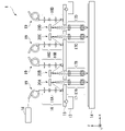
- FIG. 2 is a diagram showing the outline of the configurations of the illumination module 16, the projection module 17, and the light modulation section 20 of this embodiment.
- the illumination module 16 is arranged above the optical surface plate 15 and connected to the light source unit 18 via the optical fiber 19 .
- the lighting modules 16 include a first lighting module 16A, a second lighting module 16B, a third lighting module 16C and a fourth lighting module 16D.
- the first lighting module 16A to the fourth lighting module 16D are not distinguished, they are collectively referred to as the lighting module 16.
- FIG. 1 when the first lighting module 16A to the fourth lighting module 16D are not distinguished, they are collectively referred to as the lighting module 16.
- Each of the first lighting module 16A to the fourth lighting module 16D converts the light emitted from the light source unit 18 via the fiber 19 into a first light modulating section 20A, a second light modulating section 20B, and a third light modulating section 20C. and the fourth optical modulation section 20D.
- the lighting module 16 illuminates the light modulating section 20 .
- the light modulation section 20 is controlled based on the circuit pattern to be transferred to the exposure object, and modulates the illumination light from the illumination module, which will be described later in detail.
- the modulated light modulated by the light modulating section 20 is guided to the projection module 17 .
- the first optical modulating section 20A to the fourth optical modulating section 20D are arranged at different positions on the XY plane. In the following description, when the first optical modulation section 20A to the fourth optical modulation section 20D are not distinguished, they are collectively referred to as the optical modulation section 20.
- the projection module 17 is arranged below the optical surface plate 15 and irradiates the exposure object placed on the stage 14 with modulated light modulated by the spatial light modulator 201 .
- the projection module causes the light modulated by the light modulation section 20 to form an image on the exposure target, thereby exposing the exposure target.
- the projection module projects the pattern on the light modulating section 20 onto the exposure target.
- the projection module 17 includes first projection modules 17A to A fourth projection module 17D is included. In the following description, when the first projection module 17A to the fourth projection module 17D are not distinguished, they are collectively referred to as the projection module 17.
- a unit composed of the first illumination module 16A, the first light modulation section 20A, and the first projection module 17A is called a first exposure module.
- a unit composed of the second illumination module 16B, the second light modulation section 20B, and the second projection module 17B is called a second exposure module.
- Each exposure module is provided at a mutually different position on the XY plane, and can expose a pattern at a different position of the exposure target placed on the stage 14 .
- the stage 14 can scan-expose the entire surface of the exposure target or the entire surface of the exposure target area by moving relative to the exposure module in the X-axis direction, which is the scanning direction.
- the projection module 17 is also called a projection unit.
- the projection module 17 (projection section) may be a one-to-one system that projects the image of the pattern on the light modulation section 20 at one-to-one magnification, or may be an enlargement system or a reduction system. Also, the projection module 17 is preferably made of one or two kinds of glass materials (especially quartz or fluorite).
- the exposure apparatus 1 includes a position measuring unit (not shown) composed of an interferometer, an encoder, etc., in addition to the units described above, and measures the relative position of the stage 14 with respect to the optical surface plate 15 .
- the exposure apparatus 1 includes an AF (Auto Focus) section (not shown) that measures the position of the stage 14 or the object to be exposed on the stage 14 in the Z-axis direction, in addition to the above-described sections.
- the exposure apparatus 1 includes an alignment unit (not shown) that measures the relative positions of each pattern when another pattern is superimposed on the already exposed pattern on the exposure target.
- the AF section and/or the alignment section may have a configuration of TTL (Through the lens) which is measured via the projection module.
- FIG. 3 is a diagram showing the outline of the configuration of the exposure module of this embodiment. Taking the first exposure module as an example, an example of specific configurations of the illumination module 16, the light modulation section 20, and the projection module 17 will be described.
- the illumination module 16 includes a module shutter 161 and an illumination optical system 162.
- the module shutter 161 switches whether to guide the pulsed light supplied from the optical fiber 19 to the illumination optical system 162 .
- the illumination optical system 162 emits the pulsed light supplied from the optical fiber 19 to the light modulation section 20 through a collimator lens, a fly-eye lens, a condenser lens, etc., thereby illuminating the light modulation section 20 substantially uniformly. do.
- the fly-eye lens wavefront-divides the pulsed light incident on the fly-eye lens, and the condenser lens superimposes the wavefront-divided light onto the light modulation section.
- the illumination optical system 162 may have a rod integrator instead of the fly-eye lens.
- the light modulating section 20 has a mask.
- the mask may be a photomask or a spatial light modulator (SLM). A case where the mask is a spatial light modulator will be described below.
- the light modulation section 20 includes a spatial light modulator 201 and an off light absorption plate 202 .
- the spatial light modulator 201 includes a liquid crystal element, a digital mirror device (digital micromirror device, DMD), a magneto-optic spatial light modulator (MOSLM), and the like.
- the spatial light modulator 201 may be of a reflective type that reflects the illumination light from the illumination optical system 162, a transmissive type that transmits the illumination light, or a diffraction type that diffracts the illumination light.
- the spatial light modulator 201 can spatially and temporally modulate the illumination light. A case where the spatial light modulator 201 is composed of a digital micromirror device (DMD) will be described below as an example.
- DMD digital micromirror device
- FIG. 4 is a diagram showing an overview of the configuration of the spatial light modulator 201 of this embodiment. Description will be made using a three-dimensional orthogonal coordinate system of Xm-axis, Ym-axis, and Zm-axis in FIG.
- the spatial light modulator 201 has a plurality of micromirrors arranged in the XmYm plane.
- the micromirrors constitute elements (pixels) of the spatial light modulator 201 .
- the spatial light modulator 201 can change the tilt angle around the Xm axis and around the Ym axis. For example, the spatial light modulator 201 is turned on by tilting around the Ym axis, and turned off by tilting around the Xm axis.
- the spatial light modulator 201 controls the direction in which incident light is reflected for each element by switching the tilt direction of the micromirror for each micromirror.
- the digital micromirror device of the spatial light modulator 201 has a pixel count of about 4 Mpixels, and can switch between the ON state and the OFF state of the micromirror at a period of about 10 kHz.
- a plurality of elements of the spatial light modulator 201 are individually controlled at predetermined time intervals.
- the spatial light modulator 201 is a DMD
- the element is a micromirror
- the predetermined time interval is a period (for example, a period of 10 kHz) at which the micromirror is switched between an on state and an off state.
- the off-light absorption plate 202 absorbs light (off-light) emitted (reflected) from the elements of the spatial light modulator 201 that are turned off. Light emitted from the ON-state elements of the spatial light modulator 201 is guided to the projection module 17 .
- the projection module 17 projects the light emitted from the turned-on elements of the spatial light modulator 201 onto the exposure object.
- the projection module includes a magnification adjustment section 171 and a focus adjustment section 172 .
- Light modulated by the spatial light modulator 201 enters the magnification adjustment unit 171 .
- the magnification adjustment unit 171 adjusts the magnification of the image on the focal plane 163 of the modulated light emitted from the spatial light modulator 201, that is, the surface of the exposure object, by driving some lenses in the optical axis direction.
- the focus adjustment unit 172 drives the entire lens group in the optical axis direction so that the modulated light emitted from the spatial light modulator 201 forms an image on the surface of the exposure object measured by the AF unit described above. Then, adjust the imaging position, that is, the focus.
- the projection module 17 projects only the light image emitted from the turned-on elements of the spatial light modulator onto the surface of the exposure object. Therefore, the projection module 17 can project and expose the image of the pattern formed by the ON elements of the spatial light modulator 201 onto the surface of the exposure object. That is, the projection module 17 can form spatially modulated light on the surface of the exposure object.
- the spatial light modulator 201 can switch the micromirror between the ON state and the OFF state at a predetermined cycle (frequency) as described above, the projection module 17 exposes the temporally modulated light. It can be formed on the surface of the object. That is, the exposure apparatus 1 performs exposure by changing the substantial pupil state at an arbitrary exposure position.
- the lighting module 16 is also called a lighting system.
- the illumination module 16 (illumination system) illuminates the spatial light modulator 201 (spatial light modulation element) with the pulsed light distributed by the distributor 184 .
- the laser light source with high coherence means that when the spatial light modulator is illuminated by an optical integrator using one pulse of emitted light, and the spatial light modulator pattern is exposed, speckles are generated. It refers to pulsed light that causes a variation of more than 20% in the in-plane or pupil intensity distribution, which is a problem.
- the exposure apparatus 1 of this embodiment includes a light source unit 18 capable of reducing speckles and improving the quality of the circuit pattern transferred to the substrate.
- the light source unit 18 of this embodiment will be described below.
- FIG. 5 is a diagram showing an overview of the configuration of the light source unit 18 of this embodiment.
- the light source unit 18 includes a light source section 181 , a combining section 182 , a retarder 183 and a distribution section 184 .
- the light source unit 181 emits light with a predetermined wavelength.
- the light emitted from the light source unit 181 may be continuous light or pulsed light. A case where the light source unit 181 emits pulsed light will be described below.
- the light source unit 181 emits continuous light the continuous light is converted into pulsed light by switching a shutter (not shown) or modulated by an acoustooptic modulator (not shown).
- the light emitted from the section 181 may be substantially pulsed light.
- the light source section 181 includes a first light source section 181A to an eighth light source section 181H.
- Each of the first light source section 181A to the eighth light source section 181H has a seed light source and emits pulsed light of a predetermined wavelength.
- the light source unit 181 includes a fiber, an excitation laser diode (LD), and a wavelength conversion crystal (all not shown). The light source unit 181 causes the laser amplified by the fiber and the pumping LD to be incident on the wavelength conversion crystal to emit triple harmonic pulsed light.
- the light source provided in the light source unit 181 may be a highly coherent laser light source (eg, fiber laser) or UV-LD. Also, the light source unit 181 may be a laser light source emitting light having a wavelength of 360 nm or less.
- the synthesizing unit 182 synthesizes pulsed lights emitted from the plurality of laser light sources included in the light source unit 181 .
- the synthesizing unit 182 synthesizes the pulsed light to generate a high-intensity (high-energy) pulsed light.
- the combiner 182 emits the combined pulsed light to the retarder 183 .
- the retarder 183 repeatedly divides and combines the pulsed light emitted from the combiner 182, and combines the pulsed lights with different delay times to change the time-axis distribution of the pulsed light.
- the retarder 183 emits the pulsed light whose distribution on the time axis is changed to the distribution section 184 .
- the retarder 183 is also called a delay optical system.
- a retarder 183 delays a portion of the pulsed light.
- the retarder 183 splits a part of the pulsed light and guides it to the delaying optical path, and divides the part of the pulsed light guided to the delaying optical path with the other part of the split pulsed light. By synthesizing, the time characteristic of the pulsed light is changed.
- the distribution unit 184 distributes the pulsed light emitted from the retarder 183 to each of the plurality of optical fibers 19 . That is, the distribution unit 184 distributes pulsed light to a plurality of exposure modules.
- the distribution unit 184 guides the first pulse of pulsed light emitted from the retarder 183 to the first exposure module, and guides the second pulse of light to the second exposure module.
- the distribution section 184 can be said to be a switching section since it changes the exposure module to be guided for each pulse.
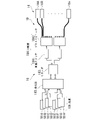
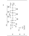
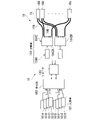
- FIG. 6 is a diagram showing the details of the configuration of the light source unit 18 of this embodiment.
- the figure shows the first light source section 181A to the fourth light source section 181D among the first light source section 181A to the eighth light source section 181H. Since the fifth light source section 181E to the eighth light source section 181H have the same configuration as the first light source section 181A to the fourth light source section 181D, description thereof will be omitted.
- the combiner 182 includes a prism mirror 1821, a polarization beam splitter 1822, a wavelength plate 1823, a wavelength plate 1824, a prism mirror 1825, a polarization beam splitter 1826 and a prism mirror 1827.
- the prism mirror 1821 guides the pulsed light (s-polarized light) emitted by the first light source section 181A to the polarizing beam splitter 1822 .
- the wave plate 1823 changes the polarization state of the pulsed light (s-polarized light) emitted from the second light source section 181B and guides the pulsed light (p-polarized light) to the polarization beam splitter 1822 .
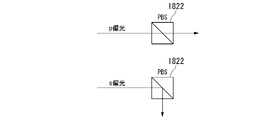
- FIG. 7 is a diagram showing an example of the polarizing beam splitter 1822 of this embodiment.
- the polarizing beam splitter 1822 transmits the pulsed light when the incident pulsed light is p-polarized light.
- the polarizing beam splitter 1822 reflects the pulsed light when the incident pulsed light is s-polarized light.
- the polarizing beam splitter 1822 reflects the pulsed light (s-polarized light) reflected by the prism mirror 1821 and guides it to the wavelength plate 1824 . Also, the polarizing beam splitter 1822 transmits the pulsed light (p-polarized light) that has passed through the wavelength plate 1823 and guides it to the wavelength plate 1824 . That is, on the wave plate 1824, the pulsed light emitted from the first light source section 181A is s-polarized (0-degree linearly polarized light), and the pulsed light emitted from the second light source section 181B is p-polarized (90-degree linearly polarized light). Incident. In other words, two types of pulsed light whose polarization directions are orthogonal to each other are synthesized at a rate of 50% each and enter the wavelength plate 1824 .
- Wave plate 1824 rotates the polarization direction of the incident pulsed light.
- the wave plate 1824 rotates the polarization direction of incident s-polarized light (0-degree linearly polarized light) to +45-degree linearly polarized light, and rotates the polarization direction of incident p-polarized light (90-degree linearly polarized light) to ⁇ 45-degree linearly polarized light.
- to Wave plate 1824 emits two types of pulsed light, +45-degree linearly polarized light and -45-degree linearly polarized light.
- the two types of pulsed light emitted from wave plate 1824 are reflected by prism mirror 1825 and guided to polarizing beam splitter 1826 .
- the polarizing beam splitter 1826 emits the incident pulsed light to the retarder 183 .
- the +45-degree linearly polarized light from the first light source section 181A and the -45-degree linearly polarized light from the second light source section 181B enter the polarizing beam splitter 1826 .
- the polarizing beam splitter 1826 reflects the s-polarized component of the incident pulsed light, ie, +45-degree s-polarized light and ⁇ 45-degree s-polarized light, and emits them to the retarder 183 .
- the polarizing beam splitter 1826 transmits the p-polarized light component of the incident pulsed light, that is, the +45-degree linearly polarized p-polarized light and the ⁇ 45-degree linearly-polarized p-polarized light, and passes through the prism mirror 1827 to the retarder 183.
- the polarizing beam splitter 1822 coaxially synthesizes the pulsed light emitted by the first light source unit 181A and the pulsed light emitted by the second light source unit 181B, and emits the light to the retarder 183 .
- the polarizing beam splitter 1822 coaxially synthesizes the pulsed light emitted from the first light source unit 181A and the pulsed light emitted from the second light source unit 181B, the respective optical axes are slightly shifted. , that is, may be combined paraxially.
- the polarizing beam splitter 1822 is of a plate type, when the p-polarized pulsed light passes through the polarizing beam splitter 1822, its optical axis is slightly translated.
- Paraxial combining can distribute the energy per unit area (power) of the pulsed light striking the optical element, ie, the energy density. As a result, deterioration including deformation of the optical element can be suppressed.
- the synthesizing unit 182 coaxially synthesizes the pulsed light emitted by the third light source unit 181 ⁇ /b>C and the pulsed light emitted by the fourth light source unit 181 ⁇ /b>D, and outputs the result to the retarder 183 .
- the light source unit 18 includes a synthesizing device.
- the synthesizing unit 182 described above is an example of a synthesizing device.
- the synthesizing device synthesizes pulsed lights emitted from a plurality of light sources.
- the pulsed light emitted from the polarizing beam splitter 1826 to the retarder 183 is also referred to as retarder incident light 183LI.
- the pulsed light emitted from the polarization beam splitter 1826 to the retarder 183 without passing through the prism mirror 1827 is also referred to as a first retarder incident light 183LI1.
- second retarder incident light 183LI2 is also referred to as two types of pulsed light beams, the first retarder incident light beam 183LI1 and the second retarder incident light beam 183LI2 emitted from the light source units 181 different from each other, are incident on the retarder 183 .
- both the first retarder incident light 183LI1 and the second retarder incident light 183LI2 are coaxial (or substantially coaxial) pulsed lights emitted from the respective light sources of the first light source section 181A to the fourth light source section 184D. (upper) is the combined light.
- the pulsed light incident on the retarder 183 may be only the first retarder incident light 183LI1.
- the retarder 183 has an input stage beam splitter 1834A, as shown in FIG. 11 and the like.
- Input stage beam splitter 1834A combines and splits first retarder incident light 183LI1 and second retarder incident light 183LI2.
- the split pulsed light enters the delay stage 1832 respectively.
- the beam splitter using polarized light has been described to synthesize and split beams, the present invention is not limited to this, and a half mirror, half prism, or the like may be used.
- the delay stage 1832 has a delay optical path, and changes the time-axis distribution of the first retarder incident light 183LI1 and the second retarder incident light 183LI2.
- the delay stage 1832 emits the pulsed light whose distribution on the time axis is changed to the distribution section 184 as the first retarder emitted light 183LO1 and the second retarder emitted light 183LO2.
- the retarder 183 (delay optical system) guides the second pulsed light along a second optical path that is longer than the first optical path that the first pulsed light travels.
- a retarder 183 (delay optical system) splits a portion of the pulsed light synthesized by the synthesizing unit 182 (synthesizing device) and guides it to the second optical path.
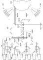
- FIG. 8 is a diagram showing an example of the configuration of the distribution unit 184 of this embodiment.
- the distributor 184 includes a rotary switch 1841 and a distributor 1842 .
- the first retarder emitted light 183LO1 is explained, and the explanation of the second retarder emitted light 183LO2 is omitted.
- illustration of the rotary switch 1841 is omitted in FIG.
- a distributor 1842 selects an optical fiber 19 into which pulsed light is incident from among a plurality of optical fibers 19 .
- distributor 1842 includes a polygon mirror device that rotates at a predetermined number of rotations. The polygon mirror device reflects the pulsed light incident from the retarder 183 in a direction according to the rotational angular velocity.
- Rotation of the polygon mirror device changes the angle of the reflection surface of the polygon mirror device with respect to the pulsed light incident from the retarder 183 . Therefore, the destination of the pulsed light incident from the retarder 183 and reflected by the reflecting surface of the polygon mirror device changes with time.
- the rotational angular velocity of the polygon mirror device is determined according to the time intervals of the light emission timings of the pulsed light. For example, when pulsed light enters the polygon mirror device in the order of a first pulse PL1, a second pulse PL2, and a third pulse PL3, the first pulse PL1 enters the first optical fiber 19A, and the second pulse PL2 enters the second pulse.
- the distributor 184 distributes the pulsed light emitted from the retarder 183 to each of the plurality of optical fibers 19 . That is, the distribution unit 184 can switch the optical fiber 19 into which the pulsed light emitted from the retarder 183 is incident every time.
- the rotary switch 1841 is provided between the retarder 183 and the distributor 1842 (not shown in FIG. 8).
- the rotary switch 1841 guides the pulsed light emitted from the retarder 183 to the first surface of the polygon mirror device during a time interval T1 (for example, between time t1 and time t2), and directs the light pulse emitted from the retarder 183 to the first surface of the polygon mirror device during a time interval T2 (for example, between time t2 and t3). pulsed light is guided to the second surface of the polygon mirror device during the interval).
- T3 for example, between times t3 and t4
- the rotary switch 1841 is constantly rotating, so that the third surface of the polygon mirror device moves to the original position of the first surface. .
- time interval T4 (eg, between times t4 and t5), similarly the fourth surface of the polygon mirror device moves to where it was on the second surface. That is, the first plane at the time interval T1 and the third plane at the time interval T3 have the same angle with respect to the pulsed light emitted from the retarder 183 . Also, the second surface at the time interval T2 and the fourth surface at the time interval T4 have the same angle with respect to the pulsed light emitted from the retarder 183 . In other words, the rotary switch 1841 changes the surface of the polygon mirror that guides the pulsed light at certain time intervals.
- the pulsed light reflected by the first surface at the time interval T1 is incident, for example, in order from the first optical fiber 19A to the fifth optical fiber 19E.
- the pulsed light reflected by the second surface at the time interval T2 is incident, for example, in order from the sixth optical fiber 19F to the tenth optical fiber 19J (not shown).
- the pulsed light reflected by the third surface at the time interval T3 is incident on the first optical fiber 19A to the fifth optical fiber 19E in order.
- the pulsed light reflected by the fourth surface at the time interval T4 enters, for example, the sixth optical fiber 19F to the tenth optical fiber 19J (not shown) in this order.
- the rotary switch 1841 changes the surface of the polygon mirror that guides the pulsed light at certain time intervals.
- the output position of the pulsed light from the optical path switching unit (for example, the polygon mirror device) and the incident position of the pulsed light on the light guide unit (for example, the optical fiber 19) are optically almost conjugate.
- the optical path switching section and the light guide section may be provided at positions where Further, the distribution unit 184 may include a lens 1843 for condensing the pulsed light reflected by the polygon mirror device at the position of the incident end of each optical fiber 19, and furthermore, a relay lens may be used to reflect the reflection of the polygon mirror device.
- the surface and the incident surface of the optical fiber 19 may be conjugated.
- the light source unit 18 is provided between an optical path switching section (for example, a polygon mirror device) and a light guide section (for example, an optical fiber 19).
- a relay lens may be provided that is optically approximately conjugate with the incident position of the pulsed light in the optical section.
- the distribution unit 184 may use a galvano-mirror or an acousto-optic modulator (AOM) that slightly vibrates the output direction of the pulsed light to change the optical path.
- AOM acousto-optic modulator
- the optical fiber 19 supplies the pulsed light distributed by the distributor 1842 to the illumination module 16.
- the plurality of optical fibers 19 are configured to guide the first pulsed light and the second pulsed light emitted from different light source units 181 to one spatial light modulator 201 .
- the first optical transmission section among the plurality of optical transmission sections guides the first pulsed light and the second pulsed light to the first spatial light modulator among the plurality of spatial light modulators 201 provided.
- the second optical transmission section among the plurality of optical transmission sections guides the first pulsed light and the second pulsed light to the second spatial light modulator among the plurality of spatial light modulators 201 provided.
- the emission position of the pulsed light from the light source (for example, the light source section 181) and the incident position at which the pulsed light is incident on the optical path switching section (for example, the distributor 1842) are optically almost conjugate.
- a light source and an optical path switching unit may be provided at the position.
- the emission position of the pulsed light from the light source section 181 and the incident position at which the pulsed light is incident on the distributor 1842 are conjugate.
- the incident position at which the pulsed light is incident on the distributor 1842 can be easily adjusted. Therefore, according to the light source unit 18 configured in this way, it is possible to easily adjust the incident position at which the pulsed light is incident on the distributor 1842 in the replacement work and the position adjustment work of the light source section 181 .
- control section 21 controls the state of the pulsed light emitted by the light source section 181 .
- An example of pulsed light emitted from the light source unit 181 will be described with reference to FIG.
- FIG. 9 is a diagram showing an example of the state of pulsed light emitted by the light source unit 181 of this embodiment.
- FIG. 1A shows an example of the state of pulsed light emitted from a conventional light source unit.
- a conventional light source unit emits pulsed light with a pulse width of 20 ns and a period of 200 kHz.
- [B] of the figure shows an example of the state of the pulsed light emitted by the light source unit 181 of the present embodiment.
- the light source unit 181 of this embodiment emits group pulse light with a pulse width of 2 ns, a pulse interval of 20 ns, the number of pulses of 10, and a period of 200 kHz.
- the plurality of light source units 181 emit group pulse light at different timings.
- the first light source section 181A and the second light source section 181B both emit group pulse light with a pulse width of 2 ns, a pulse interval of 20 ns, the number of pulses of 10, and a period of 200 kHz.
- the second light source section 181B emits pulsed light during a period of 20 ns between pulses of the group pulsed light emitted by the first light source section 181A. That is, the emission timing of the pulsed light from the first light source section 181A and the emission timing of the pulsed light from the second light source section 181B are shifted from each other.
- the first light source section 181A and the second light source section 181B have been described, but the emission timings of the first light source section 181A to the fourth light source section 181D may be shifted from each other.
- the light source unit 18 makes the states of the pulsed lights distributed by the distribution unit 184 different from each other by making the light emission timings of the plurality of pulsed lights different from each other.
- the first light source section 181A emits the first pulsed light at the first time.
- the second light source section 181B emits a second pulsed light at a second time different from the first time.
- the illumination module 16 guides the first pulsed light and the second pulsed light to the spatial light modulator 201 to illuminate the spatial light modulator 201 .
- the second light source section 181B emits the second pulsed light at the second time when the time interval from the first time is shorter than the predetermined time interval.
- the predetermined time interval is a period for switching the micromirror between the ON state and the OFF state when the spatial light modulator 201 is a DMD.
- the first light source unit 181A continuously emits first pulsed light at a predetermined cycle.
- the second light source section 181B continuously emits the second pulsed light at a predetermined cycle.
- the predetermined period is the period of the group pulse light shown in FIG. 1B (for example, a period of 200 kHz).
- Continuous emission means emission as group pulse light having a predetermined pulse width (for example, a pulse width of 2 ns), a predetermined pulse interval (for example, a pulse interval of 20 ns), and a predetermined number of pulses (for example, 10 pulses).
- the second light source unit 181B emits the second pulsed light during the time between the continuous first pulsed light emitted from the first light source unit 181A.
- the time during which the continuous first pulsed light is emitted from the first light source unit 181A is the time (for example, 200 ns) during which one group pulsed light of the first pulsed light is emitted.
- the first light source unit 181A and the second light source unit 181B emit the first pulsed light and the second pulsed light, respectively, in a predetermined cycle that is shorter than the predetermined time interval at which the elements of the spatial light modulator 201 are controlled. Inject continuously. That is, the oscillation time interval of the group pulse light (predetermined period, for example, 200 kHz) is shorter than the predetermined time interval (for example, 10 kHz) at which the plurality of elements of the spatial light modulator 201 are individually controlled. be.
- the emission timings of the plurality of pulsed lights are different from each other, and the coherence of the pulsed lights is reduced, so that the occurrence of speckles can be suppressed.
- the emission timing of the pulsed light described above may be adjusted by the control unit 21 controlling the light source unit 181 .
- Each of the first light source unit 181A to the eighth light source unit 181H described above has a seed light source, and the control unit controls each of these light sources, and also controls the oscillation timing of pulsed light for each light source. can be done.
- the control unit 21 makes the states of the pulsed lights on the spatial light modulator 201 different from each other by making the light emission timings of the plurality of pulsed lights different from each other.
- the control unit 21 is an example of a state changing unit. Further, the emission timing of the pulsed light described above may be set in advance in the light source unit 181 without being controlled by the control unit 21 .
- the wavelengths of the pulsed lights emitted by the plurality of light source units 181 may be different from each other.
- the center wavelengths of the pulsed lights of the plurality of light source units 181 are varied by several picometers to several tens of picometers.
- the permissible value of the shift amount of the center wavelength that is different for each light source unit 181 is determined, for example, by the chromatic aberration that occurs in the projection module due to the shift amount. For example, if the tolerance is 100 pm and the number of light sources is 5, each light source is evenly shifted by 20 pm. Note that the shift amount may not be uniform.
- the center wavelength is shifted for each light source section 181 to the extent that exposure failure due to chromatic aberration does not occur.
- the light source unit 181 changes the wavelength of the emitted pulsed light according to changes in the operating environment temperature.
- the plurality of light source units 181 make the wavelengths of the pulsed lights different from each other by making the operating environment temperatures different from each other.
- ⁇ be the wavelength difference between the central wavelengths of the first pulsed light and the second pulsed light
- ⁇ be the chromatic aberration of the projection optical system caused by the wavelength difference ⁇
- NA the numerical aperture of the projection optical system.
- the light source unit 18 may include a temperature control device (a heating device or a cooling device, neither of which is shown) that changes the operating environment temperature of the light source section 181 . Further, the temperature control device may be configured to change the operating environment temperature of the light source section 181 based on the control of the control section 21 . In this case, the control unit 21 controls the operating environment temperatures of the plurality of light source units 181 so that the wavelengths of the pulsed lights emitted by the plurality of light source units 181 are different from each other. The light source unit 18 can change the wavelength periodically by positively and periodically changing the temperature of the seed light, and can change the wavelength periodically within a certain range.
- a temperature control device a heating device or a cooling device, neither of which is shown
- the light source unit 18 may include a wavelength filter device (not shown) that allows transmission of a part of the wavelength band of the pulsed light emitted by the light source section 181 .
- the wavelength filter device may be configured to change the wavelength of the pulsed light to be transmitted based on the control of the controller 21 .
- the control unit 21 controls the wavelength bands transmitted by the wavelength filter devices to be different for the plurality of light source units 181 so that the wavelengths of the pulsed lights emitted by the plurality of light source units 181 are different from each other. to control.
- the light source unit 18 is an example of a state changer.
- the light source unit 18 (state changing section) makes the states of the pulsed lights distributed by the distributing section 184 different from each other by making the wavelengths of the plurality of pulsed lights different from each other.
- the wavelength of the pulsed light emitted by the first light source unit 181A and the wavelength of the pulsed light emitted by the second light source unit 181B are different from each other.
- the first light source unit 181A emits first pulsed light having a different wavelength from the second pulsed light emitted from the second light source unit 181B.
- the light source unit 18 may include a wavelength measuring device (not shown) that measures the wavelength of the emitted pulsed light.
- the control unit 21 controls the wavelength of the pulsed light emitted from the light source unit 181 based on the measurement result of the wavelength of the pulsed light by the wavelength measurement device. In other words, the controller 21 makes the states of the pulsed lights on the spatial light modulator 201 different from each other by making the wavelengths of the plurality of pulsed lights different from each other.
- the control unit 21 is an example of a state changing unit.
- the wavelengths of the plurality of pulsed lights are different from each other, and the coherence of the pulsed lights is reduced, so that the occurrence of speckles can be suppressed.
- the present invention is not limited to this.
- the phase state of the first pulsed light and the phase state of the second pulsed light may be different from each other.
- the illumination system may have a phase changing section that changes the phase state of at least one of the first pulsed light and the second pulsed light.
- the controller 21 controls the position at which the pulsed light enters the optical fiber 19 by controlling the distributor 184 .
- An example of controlling the position at which the pulsed light enters the optical fiber 19 will be described with reference to FIG.
- FIG. 10 is a diagram showing an example of positions at which the pulsed light of this embodiment enters the optical fiber 19.
- the pulsed light eg, first retarder output light 183LO1
- the distributor 1842 eg, polygon mirror device.
- the first retarder output light 183LO1 incident on the distributor 1842 is reflected in a direction based on the incident angle to the polygon mirror device and the angle of the reflecting mirror at the incident timing.
- the angle of the reflecting mirror at the timing of incidence changes as the rotation speed (angular speed) of the polygon mirror device changes.
- the first retarder output light 183LO1 reflected by the distributor 1842 enters the optical fiber 19 at the position P1.
- the rotational speed of the distributor 1842 is slower than the predetermined angular speed
- the first retarder output light 183LO1 reflected by the distributor 1842 enters the optical fiber 19 at the position P2.
- the rotational speed of the distributor 1842 is faster than the predetermined angular speed
- the first retarder output light 183LO1 reflected by the distributor 1842 enters the optical fiber 19 at the position P3.
- the reflecting surface of the polygon mirror device and the fiber entrance may be conjugated by a lens.
- the output position where the pulsed light is emitted from the optical path switching unit (for example, the polygon mirror device) and the incident position of the pulsed light in the light guide unit (for example, the optical fiber 19) are optically
- the optical path switching section and the light guide section may be provided at substantially conjugate positions. According to the light source unit 18 configured in this manner, the incident position of the fiber is almost unchanged, but the incident angle to the fiber can be changed.
- the position and angle of incidence of the pulsed light on the optical fiber 19 change as the rotation speed (angular speed) of the polygon mirror device changes.
- the position and angle of incidence of the pulsed light on the optical fiber 19 change, the path of the pulsed light guided through the optical fiber 19 changes, and the temporal characteristics of the pulsed light change.
- the controller 21 changes the rotational speed of the polygon mirror device to change the path of the pulsed light guided through the optical fiber 19, thereby changing the temporal characteristics of the pulsed light emitted from the illumination module 16.
- the light source unit 18 makes the state of the pulsed light distributed by the distributing section 184 different from each other by making the distribution timing of the pulsed light by the distributing section 184 different.
- the illumination system includes an optical transmission section that guides the first pulsed light and the second pulsed light to the spatial light modulator 201 .
- the optical fiber 19 described above is an example of an optical transmission section.
- the phase changer adjusts the angles of incidence of the first pulsed light and the second pulsed light incident on the optical transmission section (for example, the optical fiber 19).
- the above-described polygon mirror device in which the rotational speed (angular velocity) changes is an example of the phase changing section.
- the illumination system includes an optical path switching section.
- the optical path switching unit switches the optical path of the combined pulsed light and sequentially guides it to a plurality of masks.
- a polygon mirror device is an example of an optical path switching unit.
- the mask may be a photomask or a spatial light modulator.
- the control unit 21 can cause the pulsed light to be distributed by the optical path switching unit at different timings.
- the pulsed light distribution timing control by the optical path switching unit by the control unit 21 is an example of the state changing unit.
- the illumination system switches the optical paths of the first pulsed light and the second pulsed light that are sequentially oscillated from the first light source unit 181A and the second light source unit 181B, and uses a plurality of optical transmission units (for example, the optical fiber 19 ) in turn.
- the polygon mirror device described above is an example of an optical path switch.
- the optical path switching machine has a reflecting surface that reflects the first pulsed light and the second pulsed light, and changes the incident angle of the reflecting surface with respect to the first pulsed light and the second pulsed light to switch the optical path.
- the phase changer controls the optical path switch so as to adjust the incident angles of the first pulsed light and the second pulsed light entering the optical transmission section.
- phase change section may have a diffusion plate that diffuses the light incident on the spatial light modulator 201 .
- the phase change section may cause a phase change by shaking the optical fiber 19 itself.
- the exposure apparatus 1 divides and exposes the substrate by irradiating the substrate with light emitted from the plurality of spatial light modulators 201 illuminated by the first pulsed light and the second pulsed light. and a projection optical system.
- the light source unit 18 configured in this way, the temporal characteristics of the plurality of pulsed lights are different from each other, and the coherence of the pulsed lights is reduced, so that the occurrence of speckles can be suppressed.
- a diffusion plate may be arranged immediately before the incident end of each fiber 19 .
- the diffuser plate can diffuse the pulsed light and change the incident position and the incident angle of the pulsed light to the fiber, so that the phase and wavefront of the pulsed light can be changed.
- the diffused pulsed lights overlap each other and are averaged. Therefore, the phase, wavefront, intensity, etc. can be changed for each pulsed light incident on the same fiber 19 .
- the diffusion plate may have a mechanism for rotational movement and/or translational movement. By changing the position through which the pulsed light passes on the diffusion plate, the mechanism can change the state in which the pulsed light is diffused, and can change the incident position and incident angle of the pulsed light to the fiber.
- the mechanism can change the phases and wavefronts of the pulsed lights by moving the diffusion plate after the first pulse passes and before the second pulse passes.
- the phase and the movement of the wavefront diffusion plate for each pulsed light may be performed for each pulse, or may be performed for each of a plurality of pulses.
- one diffusion plate may be installed for a plurality of fibers instead of for each fiber 19 .
- the rotation speed (angular velocity) of the polygon mirror device is changed to change the incident position of the pulsed light on the optical fiber 19, the present invention is not limited to this.
- the rotation speed of the polygon mirror device may be kept constant, and the incident end of the optical fiber 19 may be moved to shift the incident position of the pulsed light.
- the incident end of the optical fiber 19 may be moved while changing the rotation speed of the polygon mirror device.
- the diffusion plate may be provided at the exit end of the optical fiber 19 . Also, the diffusion plate may be provided at the emission end of each light source.
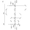
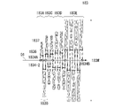
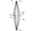
- the retarder 183 splits and synthesizes the retarder incident light 183LI to emit the retarder output light 183LO in which the state of the pulsed light is changed. Specifically, the retarder 183 divides the incident pulsed light into a plurality (for example, two) and makes the optical path length of one of the divided pulsed lights longer than the optical path length of the other pulsed light. A delay corresponding to the pulse width is caused in the pulsed light. The retarder 183 synthesizes the split pulsed lights to emit a pulsed light whose state is changed with respect to the incident pulsed light. A specific configuration of the retarder 183 will be described with reference to FIG.
- FIG. 11 is a diagram showing an overview of the configuration of the retarder 183 of this embodiment.
- the figure shows an eight-stage retarder 183 in which nine beamsplitters (eg, half-prisms) are arranged in series.
- Retarder 183 comprises input stage 1831 and delay stage 1832 .
- Input stage 1831 comprises input stage beam splitter 1834A.
- the input stage beam splitter 1834A is the beam splitter into which the pulsed light (retarder incident light 183LI) emitted from the synthesizing section 182 first enters among the nine beam splitters described above.
- the input stage beam splitter 1834A splits the incident pulsed light and outputs one of them to the input stage mirror 1835 and the other to the second stage beam splitter.
- the pulsed light reflected by the input stage mirror 1835 enters the second stage beam splitter.
- an optical path that passes through a prism mirror (for example, the input stage mirror 1835) is also called a delayed optical path, and an optical path that does not pass through a prism mirror is also called a non-delayed optical path.
- the pulsed light emitted from the input stage beam splitter 1834A (that is, the pulsed light not delayed via the non-delayed optical path) and the pulsed light reflected by the input stage mirror 1835 ( That is, the pulsed light that has been delayed via the delay optical path) is incident thereon.
- the non-delayed pulsed light and the delayed pulsed light are combined and further divided into a delayed optical path and a non-delayed optical path.
- the beam splitter included in the retarder 183 combines or splits the pulsed light by transmitting part of the pulsed light and reflecting the other part. That is, the retarder 183 (delay optical system) combines or divides the pulsed light by transmitting part of the pulsed light and reflecting the other part. Also, the beam splitter (eg, half prism) transmits or reflects the pulsed light regardless of the polarization state of the pulsed light (eg, p-polarized light and s-polarized light). A retarder 183 combines or splits the pulsed light by a beam splitter.
- the retarder 183 splits the pulsed light synthesized by the synthesizing unit 182 and delays a part of each split pulsed light. That is, the retarder 183 (delay optical system) delays part of the pulsed light synthesized by the synthesizing section 182 . More specifically, the retarder 183 (delay optical system) divides a part of the pulsed light and guides it to the delay optical path, and converts the part of the pulsed light guided to the delay optical path into the divided pulsed light. By synthesizing with a part of , the time characteristic of the pulsed light is changed. The retarder 183 (delay optical system) synthesizes pulsed light beams emitted from a plurality of light sources, divides a part of the synthesized pulsed light beams, and guides them to the delay optical path.
- the illumination system includes a splitting section that splits each of the first pulsed light and the second pulsed light into two pulsed lights; a light guiding optical system for guiding the other pulsed light that has passed through along a second optical path longer than the first optical path.
- the optical system includes a dividing unit that divides the pulsed light into a first pulsed light and a second pulsed light, and a delay optical system that guides the second pulsed light to a second optical path longer than the first optical path through which the first pulsed light passes. and a synthesizing unit that synthesizes the first pulsed light and the second pulsed light that has passed through the delay optical system.
- the illumination system guides the first pulsed light and the second pulsed light synthesized by the synthesizing section to the mask to illuminate the mask.
- the mask may be a photomask or a spatial light modulator.
- the light source unit 18 configured in this way, the temporal characteristics of the plurality of pulsed lights are different from each other, and the coherence of the pulsed lights is reduced, so that the occurrence of speckles can be suppressed.
- the delay optical path is formed by prism mirrors from the first stage to the third stage, and the delay optical path is constructed from the optical fiber 1835A having a relatively high transmittance from the fourth stage to the eighth stage.
- the constituent retarder 183 is illustrated, it is not limited to this.
- FIG. 12 is a diagram showing a first modification of the configuration of the retarder 183 of this embodiment.
- the figure shows a five-stage retarder 183 in which six beam splitters (for example, half prisms) are arranged in series.
- six beam splitters for example, half prisms
- two types of pulsed light a first retarder incident light 183LI1 and a second retarder incident light 183LI2
- enter an input stage beam splitter 1834A enter an input stage beam splitter 1834A.
- the final-stage beam splitter 1834B emits a first retarder emission light 183LO1 and a second retarder emission light 183LO2.
- the retarder 183 (delay optical system) emits pulsed light through a plurality of paths including, for example, the first retarder emitted light 183LO1 and the second retarder emitted light 183LO2.
- a retarder 183 (delay optical system) emits pulsed light to a plurality of distribution units 184 corresponding to the paths. That is, the retarder 183 of this modified example has 2 inputs and 2 outputs.
- the final stage beam splitter 1834B included in the retarder 183 (delay optical system) emits pulsed light through a plurality of paths.
- the pulsed light is guided to a plurality of distribution units 184 (optical path switching units) corresponding to respective paths.
- the delay optical system emits pulsed light through a plurality of paths, and emits the pulsed light to a plurality of optical path switching units corresponding to the paths.
- the plurality of optical path switching units may be configured by a plurality of distributors 1842, or may be configured by mutually different reflecting surfaces of one distributor 1842. FIG.
- FIG. 13 is a diagram showing a second modification of the configuration of the retarder 183 of this embodiment.
- a five-stage retarder 183 in which six beam splitters are arranged in series is shown as an example.
- the retarder 183 of this modified example is configured such that the fifth-stage delay optical path circulates between the mirrors.
- the retarder 183 of this modification includes a first orbiting mirror 1835A, a second orbiting mirror 1835B, a third orbiting mirror 1835C, and a fourth orbiting mirror 1835D.
- the first orbiting mirror 1835A to the fourth orbiting mirror 1835D constitute a fifth-stage delay optical path.
- the retarder 183 has a reflecting portion (for example, a first orbiting mirror 1835A) that reflects the second pulsed light, and an optical member that causes the reflected second pulsed light to enter the reflecting portion again.
- the optical member has a reflecting member (for example, second orbiting mirror 1835B to fourth orbiting mirror 1835D). Reflecting members (for example, second orbiting mirror 1835B to fourth orbiting mirror 1835D) reflect the second pulsed light reflected by the reflecting portion (for example, first orbiting mirror 1835A), and transmit the second pulsed light to the reflecting portion.
- the retarder 183 has an optical member that guides the pulsed light reflected by the reflector to the reflector again.
- the retarder 183 causes the optical path of the pulsed light to circulate (for example, spirally) between the reflecting section and the optical member by the reflecting section and the optical member.
- the retarder 183 configured in this way, it is possible to increase the optical path length of the delay optical path (that is, improve the speckle reduction performance) while suppressing an increase in the size of the device.
- the retarder 183 may include a beam splitter 1834C.
- the beam splitter 1834C is arranged in the circular optical path of the pulsed light formed by the first circular mirror 1835A to the fourth circular mirror 1835D. each guiding light.
- the retarder 183 configured in this way, it is possible to further increase the types of a plurality of pulsed lights having different optical path lengths, so that it is possible to further improve the speckle reduction performance while suppressing an increase in the size of the device. can.
- FIG. 14 is a diagram showing a third modification of the configuration of the retarder 183 of this embodiment.
- a four-stage retarder 183 in which five beam splitters are arranged in series is shown as an example.
- the retarder 183 of this modification includes a relay lens 1836 and a condenser mirror 1837, and a delay optical path is constructed using a Dyson optical system. More specifically, in the first stage retarder 183A, the pulsed light reflected by the input stage beam splitter 1834A is reflected by the condenser mirror 1837 via the relay lens 1836, and again via the relay lens 1836 to the second stage retarder 1834A. Incident into beam splitter 1834-2.
- the delay optical path is formed by repeating the focusing and reflection.
- the input stage beam splitter 1834A functions as a splitter that splits into the first pulsed light and the second pulsed light.
- the relay lens 1836 and the condenser mirror 1837 function as a delay optical system that guides the second pulsed light to a second optical path longer than the first optical path along which the first pulsed light passes.
- the second-stage beam splitter 1834-2 functions as a combiner that combines the first pulsed light and the second pulsed light that has passed through the delay optical system (relay lens 1836 and condenser mirror 1837).
- the relay lens 1836 has a back focus on the surface of the collector mirror 1837 .
- This back focus is the focal point of the pulsed light incident from the first stage retarder 183A and the focal point of the pulsed light emitted to the second stage retarder 183B. That is, the relay lens 1836 guides the pulsed light incident from the first stage retarder 183A and the pulsed light emitted to the second stage retarder 183B with a common focal point. That is, for the relay lens 1836, the splitting surface of the first stage retarder 183A and the splitting surface of the second stage retarder 183B are conjugate.
- the first-stage retarder 183A is also referred to as a first dividing/synthesizing section.
- the second stage retarder 183B is also referred to as a second dividing/synthesizing section. That is, the retarder 183 (delay optical system) splits the pulsed light into the first pulsed light and the second pulsed light among the plurality of beam splitters (splitting/combining units) and guides the first pulsed light to the delayed optical path. and a second stage retarder 183B (second splitting/combining unit) for combining the first and second pulsed lights emitted from the delay optical path.
- the dividing plane is conjugate.
- both pulsed lights can be regarded as substantially parallel lights, particularly when the difference in optical path length is short, the split surface of the first stage retarder 183A (first splitting/synthesizing section) and the second stage retarder 183B (second stage retarder 183B) It is not necessary to have a strictly conjugate relationship with the dividing surface of the two-divided synthesis unit).
- one pulse light may be arranged so as to be delayed by a predetermined distance.
- the relay lens 1836 is also called an optical member.
- the condensing mirror 1837 is also called a reflecting section. That is, the retarder 183 (delay optical system) includes a relay lens 1836 (optical member) and a condenser mirror 1837 (reflector). Condensing mirror 1837 (reflecting portion) reflects the first pulsed light emitted from first stage retarder 183A (first dividing/combining portion) toward second stage retarder 183B (second dividing/combining portion).
- the relay lens 1836 (optical member) is arranged on the optical path between the first stage retarder 183A (first splitting/synthesizing section) and the second stage retarder 183B (second splitting/synthesizing section).
- the first pulsed light emitted from the first splitting/synthesizing section is made incident on the collecting mirror 1837 (reflecting section), and the first pulsed light reflected by the collecting mirror 1837 (reflecting section) is transferred to the second stage retarder 183B ( second splitting/synthesizing section).
- the retarder 183 (retarding optical system) includes a reflecting portion (eg, the condenser mirror 1837) and an optical member (eg, the relay lens 1836).
- the reflecting section reflects the second pulsed light and guides it to the synthesizing section (for example, the second stage beam splitter 1834-2).
- the optical member is arranged between the dividing section (for example, the input stage beam splitter 1834A) and the reflecting section and between the reflecting section and the synthesizing section. The resulting second pulsed light is made incident on the synthesizing section.
- the retarder 183 (delay optical system) includes a splitting surface of a splitting unit (for example, the input stage beam splitter 1834A) that splits the pulsed light into a first pulsed light and a second pulsed light, and a splitting surface of the first pulsed light that has passed through the first optical path.
- the dividing unit and the combining unit are placed at a position where the combining surface of the combining unit (for example, the second beam splitter 1834-2) that combines the light and the second pulsed light that has passed through the second optical path is optically conjugate.
- the retarder 183 (delay optical system) is composed of at least two stages, the first stage retarder 183A and the second stage retarder 183B.
- the retarder 183 (delay optical system) has at least two relay lenses 1836 (optical members) arranged at opposing positions with respect to the traveling direction of the second pulsed light.
- the optical axis of one optical member and the optical axis of the other optical member are separated in the axial direction. That is, the reflector has a first reflector and a second reflector.
- the optical member includes a first optical member that causes the second pulsed light split by the dividing portion to enter the first reflecting portion, and a second optical member that causes the second pulsed light reflected by the first reflecting portion to enter the second reflecting portion. and an optical member.
- the first optical member and the second optical member are arranged with their optical axes separated from each other.
- the reflecting section (for example, the condenser mirror 1837) is provided at a position where the focal position of the optical member (for example, the relay lens 1836) is the reflecting surface that reflects the second pulsed light.
- the reflecting section (for example, the condenser mirror 1837) reflects the second pulsed light so that the second pulsed light is incident on a position different from the position in the optical member through which the second pulsed light incident on the reflecting section passes. That is, the second reflector reflects the second pulsed light and guides the second pulsed light to the first reflector again via the second optical system.
- the reflector has a third reflector.
- the optical member has a third optical member. The second reflector reflects the second pulsed light and guides the second pulsed light to the third reflector via the second optical system and the third optical system.
- the second-stage beam splitter 1834-2 of the retarder 183 has both the function of the pulse light splitting section and the function of the combining section.
- the second stage beam splitter 1834-2 (synthesizing section) splits the first pulsed light into the third pulsed light and the fourth pulsed light, and splits the second pulsed light into the fifth pulsed light and the sixth pulsed light. do.
- FIG. 15 is a diagram showing a fourth modification of the configuration of the retarder 183 of this embodiment.
- a five-stage retarder 183 in which six beam splitters are arranged in series is shown as an example.
- the retarder 183 of this modified example includes a first stage retarder 183A to a fifth stage retarder 183E.
- Each of the first-stage retarder 183A to the fifth-stage retarder 183E has a relay lens 1836 and a condenser mirror 1837, and is constructed using a Dyson optical system.
- the pulsed light reflected by the input stage beam splitter 1834A is reflected by the condenser mirror 1837 via the relay lens 1836, and again via the relay lens 1836 to the second stage retarder 1834A. Incident into beam splitter 1834-2.
- the delay optical path is formed by repeating the focusing and reflection.
- the optical path length of the delay optical path increases exponentially as the number of stages of the retarder 183 increases.
- the retarder 183 of this modification includes a plurality of relay lenses 1836 and a condenser mirror 1837 in stages after the third stage retarder 183C, and has a configuration in which the optical path is folded back in the direction of the retarder width 183W. According to the retarder 183 configured in this way, it is possible to construct a delay optical path having a longer optical path length while suppressing an increase in the dimension in the direction of the retarder width 183W.
- each stage of the retarder 183 is configured using a Dyson optical system. That is, the retarder 183 is a lens (corresponding to the relay lens 1836 in FIG. 14) that converges the second pulsed light that has passed through the beam splitter 1834 (dividing portion) onto the reflecting portion (corresponding to the condensing mirror 1837 in FIG. 14). )have.
- the lens guides the second pulsed light reflected by the condensing mirror (reflecting member) to the next-stage reflecting mirror (reflecting member).
- each stage of the retarder 183 may not be configured using the Dyson optical system.
- the retarder 183 may be configured by alternately using a delay optical path by the Dyson optical system shown in FIG. 14 and the like and a delay optical path by the prism mirror shown in FIG. 12 and the like for each stage.
- the retarder 183 has a relay lens (lens portion) that converges the second pulsed light that has passed through the beam splitter (dividing portion) onto the condensing mirror.
- the relay lens guides the second pulsed light reflected by the condenser mirror to the next-stage beam splitter.
- the beam splitter at the next stage guides the second pulsed light to the prism mirror (reflector).
- the rear-stage retarder 183 (for example, the fifth-stage retarder 183E) in which the number of turns of the optical path increases can be configured as shown in FIG.
- FIG. 16 is a diagram showing a fifth modification of the configuration of the retarder 183 of this embodiment.
- This figure shows an example of a delay optical path by a Dyson optical system, which is adopted in place of the fifth stage retarder 183E shown in FIG.
- the fifth stage retarder 183E of this modification includes a first relay lens 1836A, a first condenser mirror 1837A, a second relay lens 1836B and a second condenser mirror 1837B.
- the first condenser mirror 1837A is arranged at the back focal position of the first relay lens 1836A.
- the first light L1 incident on the first relay lens 1836A is reflected by the first condenser mirror 1837A and enters the first relay lens 1836A again as the second light L2.
- the second light L2 that has entered the first relay lens 1836A enters the second relay lens 1836B.
- the second condenser mirror 1837B is arranged at the back focal position of the second relay lens 1836B.
- the second light L2 that has entered the second relay lens 1836B is reflected by the second condenser mirror 1837B and enters the second relay lens 1836B again as the third light L3.
- the third light L3 that has entered the second relay lens 1836B enters the first relay lens 1836A.
- the third light L3 that has entered the first relay lens 1836A is reflected by the first condenser mirror 1837A and enters the first relay lens 1836A again as the fourth light L4.
- the optical axis AX2 of the second relay lens 1836B is offset from the optical axis AX1 of the first relay lens 1836A in the arrangement direction of the beam splitter 1834 (the direction D1 shown in FIGS. 15 and 16).
- the position at which the third light L3 is incident on the first relay lens 1836A is shifted in the direction D1 by the offset described above with respect to the position at which the first light L1 is incident on the first relay lens 1836A. Therefore, the incident angle at which the first light L1 enters the first collector mirror 1837A differs from the incident angle at which the third light L3 enters the first collector mirror 1837A.
- the optical path of the second light L2 reflected by the first condensing mirror 1837A and the optical path of the fourth light L4 are different from each other. become separable. Therefore, the fifth stage retarder 183E can extract the fourth light L4 as the retarder output light 183LO.
- the relay lens 1836 is arranged so that its optical axis is separated from the optical axis of the lens section.
- the retarder 183 configured in this way, it is possible to configure a delay optical path with a longer optical path length while suppressing an increase in the number of parts of the relay lens 1836 and the condenser mirror 1837 .
- the direction D1 is also referred to as the traveling direction of the second pulsed light.
- a retarder 183 delay optical system
- the set of relay lens 1836 and condenser mirror 1837 is, for example, a set of "first relay lens 1836A and first condenser mirror 1837A" and a set of "second relay lens 1836B and second condenser mirror 1837B". is.
- the delay optical path formed by the set of "first relay lens 1836A and first condenser mirror 1837A” is also referred to as the first delay optical path
- the delay line formed by the set of "second relay lens 1836B and second condenser mirror 1837B” is also referred to as the first delay optical path.
- the optical path is also called a second delay optical path.
- the optical axis of the optical member for example, the first relay lens 1836A
- the optical member for example, the optical member forming the second delay optical path
- the optical axis of the second relay lens 1836B) is offset in the direction D1 (that is, separated in the axial direction).
- FIG. 17 is a diagram showing a sixth modification of the configuration of the retarder 183 of this embodiment.
- a three-stage retarder 183 in which four beam splitters are arranged in series is shown as an example.
- the retarder 183 of this modified example is configured using two sets of Dyson optical systems arranged opposite to each other with the direction of arrangement of the beam splitters 1834 (the direction D1 in the figure) as the axis of symmetry. According to the retarder 183 configured in this manner, it is possible to configure a delay optical path with a longer optical path length while suppressing an increase in the number of parts of the relay lens 1836 and the condenser mirror 1837 .
- the luminous flux of the concave mirror (for example, the first condenser mirror 1837A or the second condenser mirror) becomes small, and a high-power laser may be damaged.
- the retardation optical system uses a beam splitter (half prism, for example) to split and synthesize light. It is also possible to adjust the transmitted/reflected light by rotating the wavelength plate.
- FIG. 18 is a diagram showing a modification of the distribution section 184.
- the distribution unit 184 of this modification includes two distributors 1842 (a first distributor 1842A and a second distributor 1842B).
- the first distributor 1842A distributes the first retarder output light 183LO1 output from the final stage beam splitter 1834B.
- the second distributor 1842B distributes the second retarder emitted light 183LO2 emitted from the final stage beam splitter 1834B.
- the distributing unit 184 of this modified example includes a first distributor 1842A that divides the first retarder output light 183LO1 and a second distributor 1842B that divides the second retarder output light 183LO2. 6 is different from the configuration of the distribution unit 184 shown in FIG.
- the rotational speeds of the two distributors 1842 can be controlled. Therefore, according to the distribution unit 184 configured as in this modification, the rotation speeds of the two distributors 1842 can be made different from each other, the coherence of the pulsed light is reduced, and the speckle reduction performance is improved. can be higher.
- FIG. 19 is a diagram showing a modification of the correspondence relationship between the light source unit 18 and the illumination module 16 of this embodiment.
- pulsed light beams in different states distributed from n (for example, two) distributors 1842 can be guided to the illumination module 16. can. Therefore, according to the exposure apparatus 1 configured as in this modified example, the state of the pulsed light emitted from the illumination module 16 can be made more diverse, the coherence of the pulsed light is reduced, and the specification It is possible to further improve the leakage reduction performance.
- FIG. 20 is a diagram showing a first modification of the light source unit 18 of this embodiment.
- the light source unit 18 of this modified example includes, for example, four light source sections 181 (first light source section 181A to fourth light source section 181D). Also, the light source unit 18 of this modified example emits two retarder outgoing light beams 183LO (a first retarder outgoing light beam 183LO1 and a second retarder outgoing light beam 183LO2) from the retarder 183 to the distributor 1842 . That is, the light source unit 18 of this modified example has a 4-input-2-output configuration.
- the synthesis unit 182 includes a prism mirror 1821, a prism mirror 1821A, a prism mirror 1821B, a polarization beam splitter 1822, a wavelength plate 1823, a prism mirror 1825, a half prism 1826A, and a prism mirror 1827 for the first light source unit 181A and the second light source unit 181B. It has The prism mirror 1821 guides the pulsed light (s-polarized light) emitted by the first light source section 181A to the polarizing beam splitter 1822 . The prism mirrors 1821A and 1821B guide the pulsed light (s-polarized light) emitted from the second light source section 181B to the wavelength plate 1823 . The wave plate 1823 changes the polarization state of the pulsed light (s-polarized light) emitted from the second light source section 181B and guides the pulsed light (p-polarized light) to the polarization beam splitter 1822 .
- the synthesizing section 182 also has a configuration corresponding to the configuration of the first light source section 181A and the second light source section 181B for the third light source section 181C and the fourth light source section 181D. That is, the synthesizing unit 182 guides the pulsed lights from the third light source unit 181C and the fourth light source unit 181D to the polarization beam splitter 1822, respectively.
- the half prism 1826A reflects part of the first light, transmits part of the second light, combines the lights, and directs the first retarder incident light 183LI1 to the input stage beam splitter 183 included in the retarder 183. Incident. Also, the half prism 1826A transmits the other part of the first light, reflects the other part of the second light, and synthesizes those lights.
- the combined light is reflected by prism mirror 1827 and enters input stage beam splitter 183 as second retarder incident light 183LI2.
- the retarder 183 changes the time-axis distribution of the pulsed light through the delay optical path between the input stage beam splitter 1834A and the final stage beam splitter 1834B.
- the retarder 183 emits the pulsed light whose distribution on the time axis is changed to the distribution section 184 as a first retarder emitted light 183LO1 and a second retarder emitted light 183LO2.
- the distribution unit 184 of this modification includes two distributors 1842 (a first distributor 1842A and a second distributor 1842B).
- the first distributor 1842A distributes the first retarder output light 183LO1 output from the final stage beam splitter 1834B.
- the second distributor 1842B distributes the second retarder emitted light 183LO2 emitted from the final stage beam splitter 1834B.
- the synthesizing unit 182 does not include the prism mirror 1827 as a configuration. , a prism mirror 1825, and a half prism 1826A.
- the retarder 183 includes a half prism 1826A and a prism mirror 1827 in addition to the configuration described above.
- the half prism 1826A can be said to be part of the combiner 182 and the input stage beam splitter of the retarder 183 .
- the first light incident on the input stage beam splitter 1834A shown in FIG. 20 and the second light reflected by the prism mirror and incident on the input stage beam splitter 1834A are incident on the input stage beam splitter 1834A.
- the half prism 1826 A and the prism mirror 1827 are part of the retarder 183 .
- This configuration is not limited to this modified example, and is the same for other embodiments and other modified examples to be described later.
- the light source unit 18 of this modification includes a plurality of light sources, an optical system, and an illumination system.
- the optical system has a splitting section, a delay optical system, and a synthesizing splitting section (for example, final stage beam splitter 1834B).
- the splitting unit splits the pulsed light emitted from each of the plurality of light sources into first pulsed light and second pulsed light.
- the delay optical system guides the second pulsed light to a second optical path longer than the first optical path followed by the first pulsed light.
- the combiner combines the first pulsed light and the second pulsed light that has passed through the delay optical system.
- the optical system emits the pulsed light synthesized by the synthesizing unit in a number (for example, two of the first retarder emitted light 183LO1 and the second retarder emitted light 183LO2) whose upper limit is the number of light sources (for example, four). .
- the optical system may be configured to split the pulsed light synthesized by the synthesizing/splitting section into at least two and emit the split light.
- the illumination system illuminates at least two masks by guiding the split pulsed light to different masks.
- the synthesizing/splitting unit synthesizes pulsed light beams based on the polarization characteristics of the pulsed light beams emitted from the plurality of light sources.
- the light source unit 18 configured in this manner, the distributions of the time axes of the plurality of pulsed lights are different from each other, and the coherence of the pulsed lights is reduced, so that the occurrence of speckles can be suppressed. . Further, according to the light source unit 18 configured to emit a smaller number (for example, two) of pulsed light than the number (for example, four) of the light source units 181, by providing the plurality of light source units 181, It is possible to emit pulsed light with reduced coherence while increasing the power of the pulsed light.
- the light source unit 18 is placed at a position where a predetermined position on the delay optical path divided by the splitter and the synthesis plane where the pulsed light is synthesized in the synthesis section are optically conjugate. may be provided. More specifically, in the light source unit 18, the pulsed light emitted from the beam splitter 1834C to the non-delayed side optical path enters the next-stage beam splitter (for example, the final-stage beam splitter 1834B) and is combined and split.
- the splitting unit and the synthesizing unit are arranged at a position where the position and the predetermined position (for example, position P5 shown in FIG. 20) of the pulsed light emitted from the beam splitter 1834C to the optical path on the delay side are optically almost conjugate.
- the light source unit 18 has a predetermined position (for example, position P5 shown in FIG. 20) on the delay optical path divided by the dividing section, and a synthesis plane (for example, position shown in FIG. 20) where pulsed light is synthesized in the synthesis section. P4) may be optically conjugated with a relay lens (not shown) on the delay optical path. This is because the retarder makes the delay optical path longer and, for example, the distance between the splitting surface of the beam splitter 1834C and the final stage beam splitter 1834B and the splitting surface is longer. This is to facilitate the relay of light by providing the .
- the pulsed light split by the splitter and guided to the delayed optical path and the pulsed light guided to the non-delayed optical path are easily synthesized on the synthesizing plane. , speckle can be further reduced.
- the optical path lengths of the respective optical paths through which the pulsed light is incident on the input stage beam splitter 1834A from the plurality of light source sections 181 may be substantially equal to each other. According to the light source unit 18 configured in this manner, the conditions of the time axes of the pulsed light beams emitted from the plurality of light source units 181 can be matched, and the adjustment of the pulsed light beams for speckle reduction can be facilitated. be able to.
- the optical path lengths of the respective optical paths through which the pulsed light is incident on the input stage beam splitter 1834A from the plurality of light source sections 181 may be different from each other. According to the light source unit 18 configured in this manner, even when pulsed light beams are emitted from a plurality of light source units 181 at the same time, variations can be given to the conditions of the time axis of the emitted pulsed light beams. , can facilitate adjustment of the pulsed light for speckle reduction.
- FIG. 21 is a diagram showing a second modification of the light source unit 18 of this embodiment.
- the light source unit 18 of this modified example includes, for example, four light source sections 181 (first light source section 181A to fourth light source section 181D). Also, the light source unit 18 of this modified example emits two retarder outgoing light beams 183LO (a first retarder outgoing light beam 183LO1 and a second retarder outgoing light beam 183LO2) from the retarder 183 to the distributor 1842 . That is, the light source unit 18 of this modified example has a 4-input-2-output configuration.
- the light source unit 18 of this modified example includes a triangular prism mirror 1828 instead of the polarizing beam splitter 1822 and wave plate 1823 of the first modified example described above.
- the synthesizing section 182 includes a prism mirror 1821C, a prism mirror 1821D, a triangular prism mirror 1828, a prism mirror 1825, a half prism 1826A and a prism mirror 1827 for the first light source section 181A and the second light source section 181B.
- the prism mirror 1821 ⁇ /b>C guides the pulsed light (s-polarized light) emitted by the first light source section 181 ⁇ /b>A to the triangular prism mirror 1828 .
- the prism mirror 1821D guides the pulsed light (s-polarized light) emitted from the second light source section 181B to the triangular prism mirror 1828.
- FIG. The triangular prism mirror 1828 guides the pulsed light emitted by the first light source section 181A and the pulsed light emitted by the second light source section 181B through the prism mirror 1825 to the half prism 1826A.
- the synthesizing section 182 also has a configuration corresponding to the configuration of the first light source section 181A and the second light source section 181B for the third light source section 181C and the fourth light source section 181D. That is, the synthesizing section 182 guides the pulsed light from the third light source section 181C and the fourth light source section 181D to the half prism 1826A via the triangular prism mirror.
- the half prism 1826A reflects part of the first light, transmits part of the second light, combines the lights, and directs the first retarder incident light 183LI1 to the input stage beam splitter 183 included in the retarder 183. Incident. Also, the half prism 1826A transmits the other part of the first light, reflects the other part of the second light, and synthesizes those lights.
- the combined light is reflected by prism mirror 1827 and enters input stage beam splitter 183 as second retarder incident light 183LI2.
- the triangular prism mirror 1828 combines the fields of view of the pulsed lights from the plurality of light source units 181 and makes them enter the half prism 1826A.
- field synthesis is to synthesize pulsed light by bringing the optical paths of the pulsed light, in other words, the optical axes, closer to each other.
- field synthesis is to bring the optical paths of the pulsed light closer to each other so that they can be relayed by a single optical system.
- the light source unit 18 of this modified example includes a light guide section including the triangular prism mirror 1828 .
- the light guide unit divides the optical paths of the pulsed light beams emitted from the plurality of light sources (eg, the first light source unit 181A and the second light source unit 181B) into a range where they can enter the dividing unit (eg, the half prism 1826A). They are brought close to each other and the pulsed light is guided to the dividing section.
- the distributions of the time axes of the plurality of pulsed lights are different from each other, and the coherence of the pulsed lights is reduced, so that the occurrence of speckles can be suppressed.
- the optical paths of the pulsed light can be positively shifted by the triangular prism mirror 1828 in consideration of the laser resistance and life of the optical components.
- the power concentration of the plurality of pulsed lights is reduced. can extend the life of the optical components.
- FIG. 22 is a diagram showing a third modification of the light source unit 18 of this embodiment.
- the light source unit 18 of this modified example includes, for example, eight light source sections 181 (first light source section 181A to eighth light source section 181H). Also, the light source unit 18 of this modified example emits two retarder outgoing light beams 183LO (a first retarder outgoing light beam 183LO1 and a second retarder outgoing light beam 183LO2) from the retarder 183 to the distributor 1842 . That is, the light source unit 18 of this modified example has an 8-input-2-output configuration.
- the light source unit 18 of this modified example combines the synthesis based on the polarization characteristics of the pulsed light using the polarization beam splitter 1822 in the first modified example and the view synthesis using the triangular prism mirror 1828 in the second modified example. By doing so, pulsed light is synthesized.
- the pulsed light from more (for example, eight) light source units 181 can be synthesized, so that the coherence of the pulsed light is further reduced and the spec It is possible to suppress the occurrence of leaks.
- FIG. 23 is a diagram showing a fourth modification of the light source unit 18 of this embodiment.
- the light source unit 18 of this modified example includes, for example, eight light source sections 181 (first light source section 181A to eighth light source section 181H). Also, the light source unit 18 of this modified example emits two retarder outgoing light beams 183LO (a first retarder outgoing light beam 183LO1 and a second retarder outgoing light beam 183LO2) from the retarder 183 to the distributor 1842 . That is, the light source unit 18 of this modified example has an 8-input-2-output configuration.
- the light source unit 18 of this modified example synthesizes eight pulsed lights by visual field synthesis using the triangular prism mirror 1828 in the above-described second modified example.
- the retarder 183 of this modification includes a polarization beam splitter 1826C, a polarization beam splitter 1826D, a wave plate 1823A and a wave plate 1823B instead of the half prism 1826B of the retarder 183 of the second modification.
- Wave plate 1823A changes the polarization state of the pulsed light incident on polarization beam splitter 1826C from the delay optical path.
- the polarizing beam splitter 1826C the pulsed light incident from the non-delayed optical path and the pulsed light incident from the wavelength plate 1823A are combined, and the combined pulsed light is emitted to position P6 shown in the figure.
- Wave plate 1823B changes the polarization state of the pulsed light incident from position P6 (that is, the pulsed light synthesized by polarization beam splitter 1826C).
- the polarizing beam splitter 1826D splits the pulsed light into the first retarder output light 183LO1 and the second retarder output light 183LO2 based on the polarization state of the pulsed light incident from the wavelength plate 1823B, and outputs the light.
- the pulsed light at the position P6 (that is, the pulsed light synthesized by the polarized beam splitter 1826C) is emitted to the distributor 1842 without the wavelength plate 1823B and the polarized beam splitter 1826D. good too.
- the light source unit 18 has an 8-input-1-output configuration.
- field combination is realized by the triangular prism mirror 1828, but it is not limited to this.
- field synthesis may be realized by the polarization beam splitter described above.
- the field of view combination may be realized by shifting the incident position of the pulsed light on the splitting surface for splitting the pulsed light.
- the method of reducing the coherence of pulsed light described above may lead to a reduction in the contrast of an integrated image in the case of scanning exposure.
- the reduction in the contrast of the integrated image in the scanning exposure occurs as an image flow due to the advance of the image during the exposure. It is preferable that the flow amount of the image is kept within about 1/3 to 1/4 of the resolution.
- the pulse emission width is 4 ns, it can be divided into a maximum of 125 ( ⁇ 128) pulses.
- the pulse width of the group pulse light obtained by synthesizing the pulse light delayed by the delay optical system of the retarder 183 is such that the product of the image flow due to the scanning speed of the exposure apparatus 1 is 1/3 or less of the resolution. is preferably set to
- a first time which is the emission timing of the first pulsed light
- the emission timing of the second pulsed light Assuming that the time difference from the second time (timing) is ⁇ , the predetermined speed is V, and the resolution is R, R/3 ⁇ V ⁇ is satisfied.
- the first light source unit 181A and the second light source unit 181B emit first pulsed light and second pulsed light that satisfy ⁇ > ⁇ (N ⁇ 2).
- ⁇ is the wavelength difference between the first pulsed light and the second pulsed light
- ⁇ is the chromatic aberration of the projection optical system caused by the wavelength difference between the first pulsed light and the second pulsed light
- NA is the projection optical system. indicates the numerical aperture of ⁇ 2 means square.
- the illumination device and exposure device of the present invention are suitable for irradiating an object with illumination light and exposing it in a lithography process.
- the flat panel display manufacturing method of the present invention is suitable for the production of flat panel displays.
Landscapes
- Physics & Mathematics (AREA)
- General Physics & Mathematics (AREA)
- Optics & Photonics (AREA)
- Engineering & Computer Science (AREA)
- Plasma & Fusion (AREA)
- Exposure And Positioning Against Photoresist Photosensitive Materials (AREA)
- Exposure Of Semiconductors, Excluding Electron Or Ion Beam Exposure (AREA)
Priority Applications (5)
| Application Number | Priority Date | Filing Date | Title |
|---|---|---|---|
| JP2023517539A JP7626207B2 (ja) | 2021-04-27 | 2022-04-26 | 照明光学系、露光装置、照明方法、デバイス製造方法及びフラットパネルディスプレイの製造方法 |
| CN202280030401.4A CN117242403A (zh) | 2021-04-27 | 2022-04-26 | 照明光学系统、曝光装置及平板显示器的制造方法 |
| KR1020237035967A KR20230160327A (ko) | 2021-04-27 | 2022-04-26 | 조명 광학계, 노광 장치 및 플랫 패널 디스플레이의 제조 방법 |
| US18/383,525 US20240085794A1 (en) | 2021-04-27 | 2023-10-25 | Illumination optical system, exposure device and method for manufacturing flat panel display |
| JP2025004055A JP2025061202A (ja) | 2021-04-27 | 2025-01-10 | 露光装置、及びデバイス製造方法 |
Applications Claiming Priority (6)
| Application Number | Priority Date | Filing Date | Title |
|---|---|---|---|
| JP2021-075408 | 2021-04-27 | ||
| JP2021-075410 | 2021-04-27 | ||
| JP2021075410 | 2021-04-27 | ||
| JP2021075408 | 2021-04-27 | ||
| JP2021-075409 | 2021-04-27 | ||
| JP2021075409 | 2021-04-27 |
Related Child Applications (1)
| Application Number | Title | Priority Date | Filing Date |
|---|---|---|---|
| US18/383,525 Continuation US20240085794A1 (en) | 2021-04-27 | 2023-10-25 | Illumination optical system, exposure device and method for manufacturing flat panel display |
Publications (1)
| Publication Number | Publication Date |
|---|---|
| WO2022230847A1 true WO2022230847A1 (ja) | 2022-11-03 |
Family
ID=83848146
Family Applications (1)
| Application Number | Title | Priority Date | Filing Date |
|---|---|---|---|
| PCT/JP2022/018810 Ceased WO2022230847A1 (ja) | 2021-04-27 | 2022-04-26 | 照明光学系、露光装置及びフラットパネルディスプレイの製造方法 |
Country Status (5)
| Country | Link |
|---|---|
| US (1) | US20240085794A1 (https=) |
| JP (2) | JP7626207B2 (https=) |
| KR (1) | KR20230160327A (https=) |
| TW (1) | TW202301035A (https=) |
| WO (1) | WO2022230847A1 (https=) |
Cited By (2)
| Publication number | Priority date | Publication date | Assignee | Title |
|---|---|---|---|---|
| JP2025061202A (ja) * | 2021-04-27 | 2025-04-10 | 株式会社ニコン | 露光装置、及びデバイス製造方法 |
| WO2025197436A1 (ja) * | 2024-03-19 | 2025-09-25 | 株式会社ニコン | 露光方法、露光装置、及びデバイス製造方法 |
Citations (7)
| Publication number | Priority date | Publication date | Assignee | Title |
|---|---|---|---|---|
| JP2002523905A (ja) * | 1998-08-20 | 2002-07-30 | オルボテック リミテッド | レーザ繰り返し率増倍器 |
| JP2004157219A (ja) * | 2002-11-05 | 2004-06-03 | Fuji Photo Film Co Ltd | 露光ヘッドおよび露光装置 |
| JP2006053240A (ja) * | 2004-08-10 | 2006-02-23 | Noritsu Koki Co Ltd | レーザー光変調装置 |
| JP2008182115A (ja) * | 2007-01-25 | 2008-08-07 | Nikon Corp | 露光方法及び露光装置並びにマイクロデバイスの製造方法 |
| JP2009300543A (ja) * | 2008-06-10 | 2009-12-24 | Orc Mfg Co Ltd | 露光描画装置 |
| JP2013061677A (ja) * | 2007-05-24 | 2013-04-04 | Asml Netherlands Bv | ドーズ量制御が可能な複数の光路を備えるレーザビーム調整システム |
| JP2017535821A (ja) * | 2014-11-27 | 2017-11-30 | カール・ツァイス・エスエムティー・ゲーエムベーハー | 複数の個々に制御可能な書込ヘッドを含むリソグラフィ装置 |
Family Cites Families (3)
| Publication number | Priority date | Publication date | Assignee | Title |
|---|---|---|---|---|
| JP2006171426A (ja) | 2004-12-16 | 2006-06-29 | Fuji Photo Film Co Ltd | 照明光学系及びそれを用いた露光装置 |
| JP5731063B2 (ja) * | 2011-04-08 | 2015-06-10 | エーエスエムエル ネザーランズ ビー.ブイ. | リソグラフィ装置、プログラマブル・パターニングデバイス、及びリソグラフィ方法 |
| TW202301035A (zh) * | 2021-04-27 | 2023-01-01 | 日商尼康股份有限公司 | 照明光學系統、曝光裝置及平板顯示器之製造方法 |
-
2022
- 2022-04-26 TW TW111115814A patent/TW202301035A/zh unknown
- 2022-04-26 WO PCT/JP2022/018810 patent/WO2022230847A1/ja not_active Ceased
- 2022-04-26 KR KR1020237035967A patent/KR20230160327A/ko active Pending
- 2022-04-26 JP JP2023517539A patent/JP7626207B2/ja active Active
-
2023
- 2023-10-25 US US18/383,525 patent/US20240085794A1/en active Pending
-
2025
- 2025-01-10 JP JP2025004055A patent/JP2025061202A/ja active Pending
Patent Citations (7)
| Publication number | Priority date | Publication date | Assignee | Title |
|---|---|---|---|---|
| JP2002523905A (ja) * | 1998-08-20 | 2002-07-30 | オルボテック リミテッド | レーザ繰り返し率増倍器 |
| JP2004157219A (ja) * | 2002-11-05 | 2004-06-03 | Fuji Photo Film Co Ltd | 露光ヘッドおよび露光装置 |
| JP2006053240A (ja) * | 2004-08-10 | 2006-02-23 | Noritsu Koki Co Ltd | レーザー光変調装置 |
| JP2008182115A (ja) * | 2007-01-25 | 2008-08-07 | Nikon Corp | 露光方法及び露光装置並びにマイクロデバイスの製造方法 |
| JP2013061677A (ja) * | 2007-05-24 | 2013-04-04 | Asml Netherlands Bv | ドーズ量制御が可能な複数の光路を備えるレーザビーム調整システム |
| JP2009300543A (ja) * | 2008-06-10 | 2009-12-24 | Orc Mfg Co Ltd | 露光描画装置 |
| JP2017535821A (ja) * | 2014-11-27 | 2017-11-30 | カール・ツァイス・エスエムティー・ゲーエムベーハー | 複数の個々に制御可能な書込ヘッドを含むリソグラフィ装置 |
Cited By (2)
| Publication number | Priority date | Publication date | Assignee | Title |
|---|---|---|---|---|
| JP2025061202A (ja) * | 2021-04-27 | 2025-04-10 | 株式会社ニコン | 露光装置、及びデバイス製造方法 |
| WO2025197436A1 (ja) * | 2024-03-19 | 2025-09-25 | 株式会社ニコン | 露光方法、露光装置、及びデバイス製造方法 |
Also Published As
| Publication number | Publication date |
|---|---|
| JPWO2022230847A1 (https=) | 2022-11-03 |
| KR20230160327A (ko) | 2023-11-23 |
| JP2025061202A (ja) | 2025-04-10 |
| US20240085794A1 (en) | 2024-03-14 |
| JP7626207B2 (ja) | 2025-02-04 |
| TW202301035A (zh) | 2023-01-01 |
Similar Documents
| Publication | Publication Date | Title |
|---|---|---|
| KR101624140B1 (ko) | 조명 광학 장치, 노광 장치, 조명 방법, 노광 방법 및 디바이스 제조 방법 | |
| US6594090B2 (en) | Laser projection display system | |
| JP2025061202A (ja) | 露光装置、及びデバイス製造方法 | |
| US6597430B1 (en) | Exposure method, illuminating device, and exposure system | |
| JP3005203B2 (ja) | 照明装置、露光装置及びデバイス製造方法 | |
| US10591824B2 (en) | Illumination optical device, illumination method, and exposure method and device | |
| JP6676940B2 (ja) | 光源装置、照明装置及びプロジェクター | |
| WO2013039240A1 (ja) | 照明光学装置、光学系ユニット、照明方法、並びに露光方法及び装置 | |
| CN115023663A (zh) | 光学装置、曝光装置、平板显示器的制造方法及器件制造方法 | |
| KR102950337B1 (ko) | 노광 장치 | |
| WO2016035666A1 (ja) | 照明装置、投射装置及び光源装置 | |
| CN117242403A (zh) | 照明光学系统、曝光装置及平板显示器的制造方法 | |
| JP5403244B2 (ja) | 空間光変調ユニット、照明光学系、露光装置、およびデバイス製造方法 | |
| JP2011114041A (ja) | 光束分割装置、空間光変調ユニット、照明光学系、露光装置、およびデバイス製造方法 | |
| JP5353408B2 (ja) | 照明光学系、露光装置、およびデバイス製造方法 | |
| WO2026062834A1 (ja) | 光装置、露光装置、及び加工装置 | |
| WO2024262020A1 (ja) | 空間光変調ユニットおよび露光装置 | |
| JP2023000088A (ja) | 光源装置及びプロジェクター |
Legal Events
| Date | Code | Title | Description |
|---|---|---|---|
| 121 | Ep: the epo has been informed by wipo that ep was designated in this application |
Ref document number: 22795760 Country of ref document: EP Kind code of ref document: A1 |
|
| ENP | Entry into the national phase |
Ref document number: 20237035967 Country of ref document: KR Kind code of ref document: A |
|
| WWE | Wipo information: entry into national phase |
Ref document number: 1020237035967 Country of ref document: KR |
|
| WWE | Wipo information: entry into national phase |
Ref document number: 202280030401.4 Country of ref document: CN |
|
| WWE | Wipo information: entry into national phase |
Ref document number: 2023517539 Country of ref document: JP |
|
| NENP | Non-entry into the national phase |
Ref country code: DE |
|
| 122 | Ep: pct application non-entry in european phase |
Ref document number: 22795760 Country of ref document: EP Kind code of ref document: A1 |