WO2022219984A1 - モジュール駆動装置及び光学装置 - Google Patents
モジュール駆動装置及び光学装置 Download PDFInfo
- Publication number
- WO2022219984A1 WO2022219984A1 PCT/JP2022/011224 JP2022011224W WO2022219984A1 WO 2022219984 A1 WO2022219984 A1 WO 2022219984A1 JP 2022011224 W JP2022011224 W JP 2022011224W WO 2022219984 A1 WO2022219984 A1 WO 2022219984A1
- Authority
- WO
- WIPO (PCT)
- Prior art keywords
- module
- wire
- fixed
- movable
- holder
- Prior art date
- Legal status (The legal status is an assumption and is not a legal conclusion. Google has not performed a legal analysis and makes no representation as to the accuracy of the status listed.)
- Ceased
Links
Images


Classifications
-
- H—ELECTRICITY
- H04—ELECTRIC COMMUNICATION TECHNIQUE
- H04N—PICTORIAL COMMUNICATION, e.g. TELEVISION
- H04N23/00—Cameras or camera modules comprising electronic image sensors; Control thereof
- H04N23/50—Constructional details
- H04N23/51—Housings
-
- G—PHYSICS
- G02—OPTICS
- G02B—OPTICAL ELEMENTS, SYSTEMS OR APPARATUS
- G02B7/00—Mountings, adjusting means, or light-tight connections, for optical elements
- G02B7/02—Mountings, adjusting means, or light-tight connections, for optical elements for lenses
- G02B7/04—Mountings, adjusting means, or light-tight connections, for optical elements for lenses with mechanism for focusing or varying magnification
-
- G—PHYSICS
- G03—PHOTOGRAPHY; CINEMATOGRAPHY; ANALOGOUS TECHNIQUES USING WAVES OTHER THAN OPTICAL WAVES; ELECTROGRAPHY; HOLOGRAPHY
- G03B—APPARATUS OR ARRANGEMENTS FOR TAKING PHOTOGRAPHS OR FOR PROJECTING OR VIEWING THEM; APPARATUS OR ARRANGEMENTS EMPLOYING ANALOGOUS TECHNIQUES USING WAVES OTHER THAN OPTICAL WAVES; ACCESSORIES THEREFOR
- G03B30/00—Camera modules comprising integrated lens units and imaging units, specially adapted for being embedded in other devices, e.g. mobile phones or vehicles
-
- G—PHYSICS
- G03—PHOTOGRAPHY; CINEMATOGRAPHY; ANALOGOUS TECHNIQUES USING WAVES OTHER THAN OPTICAL WAVES; ELECTROGRAPHY; HOLOGRAPHY
- G03B—APPARATUS OR ARRANGEMENTS FOR TAKING PHOTOGRAPHS OR FOR PROJECTING OR VIEWING THEM; APPARATUS OR ARRANGEMENTS EMPLOYING ANALOGOUS TECHNIQUES USING WAVES OTHER THAN OPTICAL WAVES; ACCESSORIES THEREFOR
- G03B5/00—Adjustment of optical system relative to image or object surface other than for focusing
Definitions
- the present disclosure relates to a module driving device and an optical device.
- a module driving device comprises a fixed-side member, a module holding body capable of holding an optical module having a lens body and an imaging device, and a module holding body capable of holding an optical module having a lens body and an imaging device, and a first driving section that moves the module holder with respect to a member; and a second driving section that rotates the module holder with respect to the stationary member so as to rotate about the optical axis.
- the first drive section includes a plurality of shape memory alloy wires provided between the movable side member including the module holder and the fixed side member
- the second driving section includes a plurality of shape-memory alloy wires provided between the movable-side member and the fixed-side member.
- the module drive device described above can achieve a smaller size than a device using a voice coil motor.
- FIG. 4 is a perspective view of the module driving device with the camera module attached;
- FIG. 4 is a perspective view of the module driving device with the camera module removed;
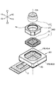
- It is an exploded perspective view of a module drive.
- 4 is a perspective view of a module holder, elastic metal members, and a base member;
- FIG. 4 is a perspective view of a metal member connected to the module holder;
- FIG. 4 is a perspective view of a metal member connected to the base member;
- FIG. 1 is a diagram of a metal member to which a shape memory alloy wire is attached;
- FIG. 1 is a diagram of a metal member to which a shape memory alloy wire is attached;
- FIG. It is a perspective view of a base member.
- FIG. 1 is a perspective view of an elastic metal member, a shape memory alloy wire, a metal member, and a conductive member
- FIG. FIG. 4 is a top view of an elastic metal member, a metal member, and a conductive member
- FIG. 4 is a diagram showing an example of a path of current flowing through a shape memory alloy wire
- FIG. 10 is a diagram showing another example of a path of current flowing through a shape memory alloy wire
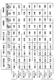
- FIG. 4 is a table showing expansion and contraction states of shape memory alloy wires when each of the five degrees of freedom of movement of the module holder is realized.
- FIG. 4A is a top view, a front view, a rear view, a left side view, and a right side view of a module holder and a base member connected by a shape memory alloy wire;
- FIG. 4 is a top view of a module holder and a base member;
- FIG. 4 is a top view of a module holder and a base member; It is a front view of a module holder and a base member. It is a right view of a module holding body and a base member.
- FIG. 4 is a top view of a module holder and a base member; 1 is an exploded perspective view of a camera module;
- FIG. 10 is a table showing expansion and contraction states of the module-side shape memory alloy wire when each of the five degrees of freedom of movement of the lens holder is realized.
- FIG. 10 is a table showing expansion and contraction states of the module-side shape memory alloy wire when each of the five degrees of freedom of movement of the lens holder is realized.
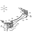
- FIG. 1A and 1B are perspective views of the module driving device 101.
- FIG. 1A is an upper perspective view of the module driving device 101 with a camera module MD, which is an example of an optical module, attached
- FIG. 1B is a module driving device with the camera module MD removed.
- 1 is a top perspective view of device 101.
- FIG. FIG. 2 is an exploded perspective view of the module driving device 101.
- the module driving device 101 is a camera module driving device.
- X1 represents one direction of the X-axis that constitutes the three-dimensional orthogonal coordinate system
- X2 represents the other direction of the X-axis
- Y1 represents one direction of the Y-axis forming the three-dimensional orthogonal coordinate system
- Y2 represents the other direction of the Y-axis
- Z1 represents one direction of the Z-axis forming the three-dimensional orthogonal coordinate system
- Z2 represents the other direction of the Z-axis.
- the X1 side of the module drive device 101 corresponds to the front side (front side) of the module drive device 101
- the X2 side of the module drive device 101 corresponds to the rear side of the module drive device 101.
- the Y1 side of the module driving device 101 corresponds to the left side of the module driving device 101
- the Y2 side of the module driving device 101 corresponds to the right side of the module driving device 101
- the Z1 side of the module driving device 101 corresponds to the upper side of the module driving device 101 (object side)
- the Z2 side of the module driving device 101 corresponds to the lower side of the module driving device 101 (image sensor side).
- the module drive device 101 includes a cover member 4 that is part of the fixed side member FB, as shown in FIGS. 1A, 1B, and 2 .
- the cover member 4 is configured to function as part of the housing HS that covers each member.
- the cover member 4 is made of non-magnetic metal.
- the cover member 4 may be made of a magnetic metal.
- the cover member 4 has a box-like outer shape that defines the housing portion 4S. A camera module MD is accommodated in the accommodating portion 4S.
- the camera module MD is an example of an optical module, and includes a circuit board 7, a lens driving device LD, a lens body LS held by the lens driving device LD, and a and an image sensor IS mounted on the circuit board 7 .
- An IR cut filter may be arranged between the lens body LS and the image sensor IS.
- the camera module MD is a camera module that includes a shape memory alloy wire-type driving unit.
- the camera module MD may be a camera module having a drive unit of another type such as a voice coil motor type including a magnet and a coil or a piezoelectric type.
- the circuit board 7 is connected to the outside through the flexible board 3 .
- the drive unit of the camera module MD is configured to move the lens body LS along the Z-axis direction, which is the optical axis direction of the lens body LS, on the Z1 side of the imaging element IS. there is By moving the lens body LS in this manner, the camera module MD can realize an automatic focus adjustment function, which is one of the lens adjustment functions. Specifically, the camera module MD moves the lens body LS in a direction away from the image sensor IS to enable macro photography, and moves the lens body LS in a direction to approach the image sensor IS to enable infinity photography. do.
- the camera module MD may be configured such that the lens body LS can be moved in at least one of the X-axis direction and the Y-axis direction. By moving the lens body LS in this way, the camera module MD may implement a camera shake correction function, which is another lens adjustment function.
- FIG. 1A shows the state of the lens body LS and the lens driving device LD when the camera module MD is in the neutral state (neutral position).
- the lens body LS is translatable along the Z-axis direction with respect to the housing of the lens driving device LD
- the neutral state of the camera module MD is the lens body LS positioned in the middle of the movable range in the Z-axis direction.
- the lens body LS is positioned at the center of the movable range in the Z-axis direction. The same applies when the lens body LS is translatable along the X-axis direction and when the lens body LS is translatable along the Y-axis direction.
- the initial state of the camera module MD when power is not supplied to the drive unit may be the neutral state.
- the imaging surface of the image sensor IS is perpendicular to the optical axis OA of the lens body LS arranged to face the image sensor IS.
- the central axis of the imaging device IS (imaging surface) coincides with the optical axis OA of the lens body.
- the imaging surface of the imaging device IS is a plane parallel to the upper surface of the imaging device IS on the subject side.
- the camera module MD may be a fixed-focus camera module. That is, the lens body LS may be arranged so as not to move relative to the image sensor IS.
- the cover member 4 includes a rectangular tubular outer peripheral wall portion 4A and a rectangular ring-shaped top plate provided so as to be continuous with the upper end (Z1 side end) of the outer peripheral wall portion 4A. and a part 4B.
- An octagonal opening 4K is formed in the center of the top plate portion 4B.
- the outer peripheral wall portion 4A includes a first side plate portion 4A1 to a fourth side plate portion 4A4.
- the first side plate portion 4A1 and the third side plate portion 4A3 face each other, and the second side plate portion 4A2 and the fourth side plate portion 4A4 face each other.
- the first side plate portion 4A1 and the third side plate portion 4A3 extend perpendicularly to the second side plate portion 4A2 and the fourth side plate portion 4A4.
- the cover member 4 is joined to the base member 8 with an adhesive, as shown in FIG. 1A.
- the base member 8 constitutes a housing HS together with the cover member 4 .
- the drive section DM, the camera module MD, the module holder 2, the metal member 5, the elastic metal member 6, the circuit board 7, and the like are accommodated inside the housing HS.
- a flexible substrate 3 is attached to the lower surface (surface on the Z2 side) of the base member 8 that constitutes the housing HS.
- the imaging element IS is provided with a cross pattern
- the flexible substrate 3 is provided with a coarse dot pattern
- the circuit board 7 is provided with a fine dot pattern.
- the drive unit DM includes a shape memory alloy wire SA, which is an example of a shape memory actuator.
- the shape memory alloy wires SA include first wires SA1 to eighth wires SA8 having substantially the same length and substantially the same diameter.
- the shape memory alloy wire SA increases in temperature when current flows, and contracts according to the increase in temperature.
- the drive unit DM can move the module holder 2 using contraction of the shape memory alloy wires SA. When one or more of the first to eighth wires SA1 to SA8 contract, the module holder 2 moves, and another one or more of the shape memory alloy wires SA are elongated by the movement ( decompressed).
- the driving part DM is configured so that the movable side member MB can move with five degrees of freedom. Movements with five degrees of freedom include translation in a second direction (X-axis direction) perpendicular to the first direction (Z-axis direction), which is the direction of the optical axis, and a third direction (Y-axis direction) perpendicular to the first and second directions. direction), rotation about a first direction (Z-axis), rotation about a second direction (X-axis), and rotation about a third direction (Y-axis).
- the first direction is parallel to the first rotation axis RX1 that coincides with the optical axis OA of the lens body LS
- the second direction is parallel to the second rotation axis RX2.
- the third direction is parallel to the third rotation axis RX3.
- the axis line of the second rotation axis RX2 is orthogonal to the axis line of the first rotation axis RX1
- the axis line of the third rotation axis RX3 is orthogonal to the axis line of the first rotation axis RX1 and the axis line of the second rotation axis RX2.
- the optical axis direction includes the direction of the optical axis OA with respect to the lens body LS and the direction parallel to the optical axis OA.
- the second rotation axis RX2 is also called a first swing axis
- the third rotation axis RX3 is also called a second swing axis.
- the flexible substrate 3 is a flexible substrate on which wiring patterns are formed for connecting the module driving device 101 and devices outside the module driving device 101 .
- the flexible substrate 3 is a flexible printed circuit board configured to be repeatedly deformable.
- the circuit board 7 is a board on which the imaging element IS is mounted.
- the circuit board 7 is a rigid circuit board.
- the movable side member MB is a member that is driven by the drive section DM.
- the movable side member MB includes a module holder 2 capable of holding the camera module MD.
- the camera module MD may be included in the movable side member MB.
- the module holder 2 is configured to hold the camera module MD having the lens body LS and the imaging element IS.
- the module holder 2 is formed by injection molding synthetic resin such as liquid crystal polymer (LCP).
- LCP liquid crystal polymer
- the module holder 2 includes a frame 2F that is substantially rectangular in top view, and movable-side pedestals formed at two of the four corners of the frame 2F. 2D, and projections 2S formed at the remaining two of the four corners of the frame 2F.
- the camera module MD is configured to be bonded to the inner surface of the frame 2F with an adhesive.
- another member such as a case or cover capable of accommodating the camera module MD may be arranged between the frame 2F and the camera module MD.
- the other member such as the case or cover may be made of metal or synthetic resin.
- the module holder 2 may constitute a part of the camera module MD.
- the module holder 2 may be integrated with the housing of the camera module MD.
- the housing of the camera module MD is, for example, the cover member 4x.
- the movable-side pedestal portion 2D includes a first movable-side pedestal portion 2D1 and a second movable-side pedestal portion 2D2.
- the first movable-side pedestal portion 2D1 and the second movable-side pedestal portion 2D2 are arranged so as to face each other across the first rotation axis RX1 (optical axis OA).
- the projecting portion 2S includes a first projecting portion 2S1 and a second projecting portion 2S2.
- the first projecting portion 2S1 and the second projecting portion 2S2 are arranged to face each other with the first rotation axis RX1 interposed therebetween.
- the movable-side pedestal portion 2D and the projecting portion 2S are arranged so as to correspond to the four corners of the module holding body 2 (frame body 2F) having a substantially rectangular outer shape when viewed from above, and , are arranged alternately.
- a part of the elastic metal member 6 is placed on each of the two movable-side pedestals 2D, as shown in FIG.
- FIG. 3 is a perspective view of the elastic metal member 6 connected to the module holder 2 and the base member 8, showing the positional relationship between the module holder 2 and the base member 8 and the elastic metal member 6.
- the module holder 2 has a fine dot pattern and the base member 8 has a coarse dot pattern.
- illustration of members other than the module holder 2, the elastic metal member 6, and the base member 8 is omitted for clarity.
- the elastic metal member 6 is configured to movably support the module holder 2 with respect to the fixed side member FB (base member 8).
- the elastic metal member 6 is made of a conductive metal plate mainly made of, for example, a copper alloy, a titanium-copper alloy (titanium-copper), or a copper-nickel alloy (nickel-tin-copper).
- the base member 8 is formed by injection molding using synthetic resin such as liquid crystal polymer (LCP).
- LCP liquid crystal polymer
- the base member 8 has a substantially rectangular outline in top view and has an opening 8K in the center.
- the base member 8 has four side portions 8E (first side portion 8E1 to fourth side portion 8E4) arranged to surround the opening 8K.
- the base member 8 includes fixed side pedestals 8D formed at two of the four corners of the base member 8, as shown in FIG.
- the fixed-side pedestal portion 8D protrudes upward (in the Z1 direction) from the plate-like base portion of the base member 8 .
- the fixed side pedestal portion 8D includes a first fixed side pedestal portion 8D1 and a second fixed side pedestal portion 8D2.
- the first fixed side seat portion 8D1 and the second fixed side seat portion 8D2 are arranged so as to face each other with the first rotation axis RX1 interposed therebetween.
- the first fixed-side pedestal portion 8D1 is arranged so as to face the first projecting portion 2S1 of the module holder 2 in the radial direction about the Z-axis.
- the side pedestal portion 8D2 is arranged so as to face the second projecting portion 2S2 of the module holder 2. As shown in FIG.
- the elastic metal member 6 is configured to connect the movable side pedestal portion 2D formed on the module holder 2 and the fixed side pedestal portion 8D formed on the base member 8 .
- the elastic metal member 6 includes a first fixed portion 6e1 attached to a first fixed-side pedestal portion 8D1 formed on the base member 8, and a A second fixing portion 6e2 attached to the first movable side pedestal portion 2D1, a third fixing portion 6e3 attached to the second fixed side pedestal portion 8D2 formed on the base member 8, and a third fixing portion 6e3 formed on the module holder 2. 2 and a fourth fixing portion 6e4 attached to the movable side pedestal portion 2D2.
- FIG. 3 the elastic metal member 6 includes a first fixed portion 6e1 attached to a first fixed-side pedestal portion 8D1 formed on the base member 8, and a A second fixing portion 6e2 attached to the first movable side pedestal portion 2D1, a third fixing portion 6e3 attached to the second fixed side pedestal portion 8D2 formed on the base member 8, and a third fixing portion
- the elastic metal member 6 includes an elastically deformable first arm portion 6g1 connecting the first fixing portion 6e1 and the second fixing portion 6e2, a second fixing portion 6e2 and a third fixing portion 6e3. an elastically deformable second arm portion 6g2 that connects the third fixing portion 6e3 and the fourth fixing portion 6e4, and an elastically deformable third arm portion 6g3 that connects the fourth fixing portion 6e4 and the first fixing portion 6e1 It has an elastically deformable fourth arm portion 6g4 that connects the .
- the metal member 5 is configured so that the end of the shape memory alloy wire SA is fixed.
- the metal member 5 includes a fixed side metal member 5F and a movable side metal member 5M, as shown in FIG.
- the stationary metal member 5 ⁇ /b>F is configured to be fixed to the stationary pedestal portion 8 ⁇ /b>D of the base member 8 .
- the movable metal member 5 ⁇ /b>M is configured to be fixed to the movable pedestal portion 2 ⁇ /b>D of the module holder 2 .
- the fixed-side metal member 5F is also called a fixed-side terminal plate, and includes a first fixed-side terminal plate 5F1 to an eighth fixed-side terminal plate 5F8.
- the movable-side metal member 5M is also called a movable-side terminal plate, and includes a first movable-side terminal plate 5M1 and a second movable-side terminal plate 5M2.
- FIG. 4A is a perspective view of the module holder 2 to which the movable-side metal member 5M (movable-side terminal plate) is attached.
- FIG. 4B is a perspective view of the base member 8 to which the fixed-side metal member 5F (fixed-side terminal plate) is attached.
- the movable metal member 5M has a dot pattern
- the fixed metal member 5F has a dot pattern.
- the first movable terminal plate 5M1 is fixed to the X1 side wall (front mounting surface) and the Y1 side wall (left mounting surface) of the first movable pedestal portion 2D1. Specifically, in a state in which the groove 2G (see FIG. 2) formed on the upper surface of the first movable-side pedestal portion 2D1 and the bent piece BP formed on the first movable-side terminal plate 5M1 are engaged with each other, the first The movable terminal plate 5M1 is fixed to the first movable pedestal 2D1 with an adhesive.
- the adhesive is, for example, a photocurable adhesive.
- the photocurable adhesive is, for example, an ultraviolet curable adhesive or a visible light curable adhesive.
- the second movable terminal plate 5M2 is fixed to the X2 side wall (rear mounting surface) and the Y2 side wall (right mounting surface) of the second movable pedestal portion 2D2. Specifically, in a state in which the groove 2G (see FIG. 2) formed on the upper surface of the second movable-side pedestal portion 2D2 and the bent piece BP formed on the second movable-side terminal plate 5M2 are engaged with each other, the second The movable terminal plate 5M2 is fixed to the second movable pedestal 2D2 with an adhesive.
- the first stationary terminal plate 5F1 and the second stationary terminal plate 5F2 are located on the X1 side of the first stationary seat 8D1 arranged along the first side 8E1 of the base member 8. It is fixed to the side wall (front mounting surface). Specifically, the first stationary terminal plate 5F1 and the second stationary terminal plate 5F2 are fixed to the first stationary pedestal portion 8D1 with an adhesive.
- the adhesive is, for example, a photocurable adhesive.
- the photocurable adhesive is, for example, an ultraviolet curable adhesive or a visible light curable adhesive.
- the third stationary terminal plate 5F3 and the fourth stationary terminal plate 5F4 (not visible in FIG.
- the second stationary pedestal 8D2 are attached to the second stationary pedestal 8D2 arranged along the second side 8E2 of the base member 8 It is fixed to the side wall (left mounting surface) on the Y1 side.
- the fifth fixed side terminal plate 5F5 and the sixth fixed side terminal plate 5F6 are arranged along the third side 8E3 of the base member 8 on the X2 side of the second fixed side pedestal portion 8D2. side wall (rear mounting surface).
- the seventh stationary terminal plate 5F7 and the eighth stationary terminal plate 5F8 are arranged along the fourth side 8E4 of the base member 8 on the Y2 side wall (right mounting surface) of the first stationary pedestal 8D1. ).
- the shape memory alloy wire SA extends along the inner surface of the outer peripheral wall portion 4A of the cover member 4, and is configured to movably support the movable side member MB with respect to the fixed side member FB.
- the shape memory alloy wires SA include first wires SA1 to eighth wires SA8 as shown in FIG. It is configured to be able to movably support the module holder 2 .
- each of the first wire SA1 to the eighth wire SA8 has one end fixed to the stationary metal member 5F by crimping or welding, and the other end is crimped or welded. is fixed to the movable-side metal member 5M.
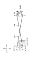
- FIG. 5A shows a seventh wire SA7 attached to each of the second movable terminal plate 5M2 and the seventh fixed terminal plate 5F7, and a wire SA7 attached to each of the second movable terminal plate 5M2 and the eighth fixed terminal plate 5F8. It is a figure when the 8th wire SA8 attached is seen from the Y2 side (right side).
- FIG. 5B shows a seventh wire SA7 attached to each of the second movable side terminal plate 5M2 and the seventh fixed side terminal plate 5F7, and each of the second movable side terminal plate 5M2 and the eighth fixed side terminal plate 5F8.
- FIGS. 5A and 5B It is a figure when the 8th wire SA8 attached is seen from the X1 side (front side).
- the positional relationship of each member shown in FIGS. 5A and 5B corresponds to the positional relationship when the module drive device 101 is assembled. 5A and 5B, illustration of other members is omitted for clarity. Also, the following description with reference to FIGS. 5A and 5B relates to the combination of the seventh wire SA7 and the eighth wire SA8, the combination of the first wire SA1 and the second wire SA2, the third wire SA3 and the fourth wire SA4. and the combination of the fifth wire SA5 and the sixth wire SA6.
- one end of the seventh wire SA7 is fixed to the seventh fixed terminal plate 5F7 at the holding portion J2 of the seventh fixed terminal plate 5F7, and the other end of the seventh wire SA7 is fixed to the second movable terminal plate 5F7. It is fixed to the second movable side terminal plate 5M2 at the lower holding portion J1 of the terminal plate 5M2.
- one end of the eighth wire SA8 is fixed to the eighth fixed terminal plate 5F8 at the holding portion J4 of the eighth fixed terminal plate 5F8, and the other end of the eighth wire SA8 is fixed to the second movable terminal plate. It is fixed to the second movable side terminal plate 5M2 at the upper holding portion J3 of 5M2.
- the holding portion J1 is formed by bending a portion of the second movable terminal plate 5M2. Specifically, a portion of the second movable terminal plate 5M2 forms a holding portion J1 by being bent while sandwiching the end (the other end) of the seventh wire SA7. An end (the other end) of the seventh wire SA7 is fixed to the holding portion J1 by welding. The same applies to the holding portions J2 to J4.
- the seventh wire SA7 and the eighth wire SA8 are arranged so as to be twisted relative to each other (three-dimensionally intersect when viewed from the Y2 side). That is, the seventh wire SA7 and the eighth wire SA8 are arranged so as not to contact each other (become non-contact).
- FIG. 6 is a perspective view of the base member 8.
- FIG. Specifically, the upper view of FIG. 6 is a perspective view of the base member 8 with the conductive member CM removed, and the central view of FIG. 6 is a perspective view of the base member 8 in which the conductive member CM is embedded.
- the conductive member CM is given a dot pattern for clarity.
- the base member 8 is configured to function as a fixed-side wire support section that supports one end of each of the first wire SA1 to the eighth wire SA8. Further, the module holder 2 is configured to function as a movable wire support section that supports the other ends of the first to eighth wires SA1 to SA8. With this configuration, the movable member MB is supported by the first wire SA1 to the eighth wire SA8 so as to be movable with respect to the fixed member FB with five degrees of freedom.
- the fixed side pedestal portion 8D is formed on the upper surface of the base member 8 on the subject side (Z1 side surface).
- the fixed side pedestal portion 8D includes a first fixed side pedestal portion 8D1 and a second fixed side pedestal portion 8D2.
- the first fixed side seat portion 8D1 and the second fixed side seat portion 8D2 are arranged to face each other with the first rotation axis RX1 interposed therebetween.
- a conductive member CM formed of a metal plate containing a material such as copper, iron, or an alloy containing them as a main component is embedded by insert molding.
- the conductive member CM includes a connecting portion ED exposed on the lower surface (Z2 side surface) of the base member 8 and extending outward, and an upper surface (Z1 side surface) of the fixed side pedestal portion 8D of the base member 8 (Z1 side surface). ).
- the conductive member CM includes a first conductive member CM1 and a second conductive member CM2.
- the first conductive member CM1 includes a first connection portion ED1 and a first joint surface portion CP1
- the second conductive member CM2 includes a second connection portion ED2 and a second joint surface portion CP2.
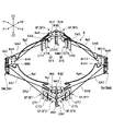
- FIGS. 7A and 7B are diagrams showing the positional relationship among the metal member 5, the elastic metal member 6, the conductive member CM, and the shape memory alloy wire SA.
- FIG. 7A is a perspective view of each member (metal member 5, elastic metal member 6, conductive member CM, and shape memory alloy wire SA)
- FIG. 7B is a top view of each member.
- dot patterns are given to the movable-side metal member 5M and the conductive member CM for clarity.
- illustration of the shape memory alloy wire SA is omitted for clarity.
- the elastic metal member 6 includes a first fixed portion 6e1 fixed to the first fixed side pedestal portion 8D1 (see FIG. 2) of the base member 8, and a first movable side portion of the module holder 2.
- the first fixing portion 6e1 has a first through hole 6H1 and a second through hole 6H2 through which the upwardly protruding columnar protrusion 8T (see FIG. 4B) formed on the first fixed side pedestal portion 8D1 is inserted. , and a third through hole 6H3 used for bonding with the first bonding surface portion CP1 (see the lower diagram of FIG. 6) of the first conductive member CM1.
- the fixing between the elastic metal member 6 and the projecting portion 8T is achieved by subjecting the projecting portion 8T to hot crimping or cold crimping.
- the fixing between the elastic metal member 6 and the projecting portion 8T may be realized by an adhesive.
- the elastic metal member 6 and the first conductive member CM1 are joined together by welding such as laser welding.
- the joint between the elastic metal member 6 and the first conductive member CM1 may be realized by solder, a conductive adhesive, or the like.
- the second fixing portion 6e2 has a fourth through hole 6H4 and a fifth through hole 6H5 through which the upwardly projecting columnar protrusion 2T (see FIG. 4A) formed on the first movable side pedestal portion 2D1 is inserted. and a sixth through-hole 6H6 used for joining with the tip of the bent piece BP (see FIG. 4A) of the first movable-side terminal plate 5M1.
- the fixing of the elastic metal member 6 and the projecting portion 2T is achieved by subjecting the projecting portion 2T to hot crimping or cold crimping.
- the fixing between the elastic metal member 6 and the projecting portion 2T may be realized by an adhesive.
- the elastic metal member 6 and the bent piece BP of the first movable terminal plate 5M1 are joined together by welding such as laser welding.
- the joint between the elastic metal member 6 and the bent piece BP may be realized by solder, a conductive adhesive, or the like.
- Each of the first arm portion 6g1 to the fourth arm portion 6g4 of the elastic metal member 6 is an elastically deformable arm portion having four curved portions. Therefore, the module holder 2 is movable with respect to the base member 8 (fixed member FB) not only in the direction parallel to the first rotation axis RX1, but also in the direction intersecting the first rotation axis RX1.
- the elastic metal member 6 is configured to have two-fold rotational symmetry with respect to the first rotation axis RX1. Therefore, the elastic metal member 6 hardly adversely affects the weight balance of the module holder 2 . In addition, the elastic metal member 6 has almost no adverse effect on the weight balance of the movable side member MB supported by the eight shape memory alloy wires SA (first wire SA1 to eighth wire SA8).
- the fixed-side metal member 5F has a connection portion CT (see FIGS. 5A and 5B) and is configured to be joined to the conductive pattern PT of the flexible substrate 3 via the connection portion CT.
- the connecting portion CT includes a first connecting portion CT1 to an eighth connecting portion CT8.
- the flexible board 3 includes, as shown in FIG. 2, a substantially rectangular inner portion 3i attached to the lower surface of the circuit board 7 and a substantially rectangular annular outer portion 3e attached to the lower surface of the base member 8. .
- a first conductive pattern PT1 to a tenth conductive pattern PT10 are formed in the outer portion 3e, and a large number of conductive patterns (not shown) used for connection with the circuit board 7 on which the imaging element IS is mounted are formed in the inner portion 3i. ) is formed.
- a substantially U-shaped slit (opening) is formed between the inner portion 3i and the outer portion 3e so that the movement of the inner portion 3i is not hindered.
- the first connecting portion CT1 of the first fixed-side terminal plate 5F1 is joined to the first conductive pattern PT1 (see FIG. 2) of the flexible substrate 3 by soldering.
- the second connection portion CT2 of the second fixed terminal plate 5F2 is soldered to the second conductive pattern PT2 (see FIG. 2) of the flexible substrate 3, and the third fixed terminal plate 5F3 is The third connection portion CT3 is joined to the third conductive pattern PT3 (see FIG. 2) of the flexible substrate 3 by soldering, and the fourth connection portion CT4 of the fourth fixed terminal plate 5F4 is soldered. It is joined to the fourth conductive pattern PT4 (see FIG.
- the first connection portion ED1 of the first conductive member CM1 is soldered to the ninth conductive pattern PT9 (see FIG. 2) of the flexible substrate 3, and the second connection portion ED2 of the second conductive member CM2 is It is joined to the tenth conductive pattern PT10 (see FIG. 2) of the flexible substrate 3 by soldering.
- both the ninth conductive pattern PT9 and the tenth conductive pattern PT10 are connected to a ground terminal (not shown).
- the connection portion ED and the conductive pattern PT of the flexible substrate 3 may be joined by a conductive adhesive.
- the bent piece BP of the first movable terminal plate 5M1 is joined to the second fixed portion 6e2 of the elastic metal member 6 by welding such as laser welding, as shown in FIG. 7B.
- the bent piece BP of the second movable side terminal plate 5M2 is joined to the fourth fixed portion 6e4 of the elastic metal member 6 by welding such as laser welding.
- the first stationary terminal plate 5F1, the second stationary terminal plate 5F2, the seventh stationary terminal plate 5F7, and the eighth stationary terminal plate 5F8 are the first stationary portion of the elastic metal member 6, as shown in FIG. 7B. 6e1, and is not in contact with the first fixing portion 6e1 of the elastic metal member 6.
- the first fixed portion 6e1 of the elastic metal member 6 is joined to the first joint surface portion CP1 of the first conductive member CM1 by welding such as laser welding.
- the third stationary terminal plate 5F3 to the sixth stationary terminal plate 5F6 are arranged apart from the third stationary portion 6e3 of the elastic metal member 6, as shown in FIG. 7B. is not in contact with the third fixing portion 6e3.
- the third fixing portion 6e3 of the elastic metal member 6 is joined to the second joint surface portion CP2 of the second conductive member CM2 by welding such as laser welding.
- FIGS. 8A and 8B are perspective views of a portion of the arrangement shown in FIG. 7A.
- the first conductive member CM1 and the second movable terminal plate 5M2 are given rough dot patterns
- the seventh stationary terminal plate 5F7 and the eighth stationary terminal plate 5F8 has a fine dot pattern
- the elastic metal member 6 has an even finer dot pattern.
- FIG. 8A shows the state when the seventh connection portion CT7 of the seventh stationary terminal plate 5F7 is connected to a high potential and the first connection portion ED1 of the first conductive member CM1 is connected to a low potential.
- FIG. 8B shows that the eighth connection portion CT8 of the eighth fixed terminal plate 5F8 is connected to a high potential, and the first connection portion ED1 of the first conductive member CM1 is connected to a low potential. shows the path of the current when The following description relates to the path of the current flowing through the seventh wire SA7 or the eighth wire SA8, but the path of the current flowing through the first wire SA1 or the second wire SA2, the current flowing through the third wire SA3 or the fourth wire SA4. The same applies to the path and the path of the current flowing through the fifth wire SA5 or the sixth wire SA6.
- the current flows as indicated by the arrow AR1 in FIG. 8A. flows through the seventh connecting portion CT7 to the seventh stationary terminal plate 5F7. After that, the current flows through the seventh fixed terminal plate 5F7 as indicated by arrow AR2, through the seventh wire SA7 as indicated by arrow AR3, and further through the second movable terminal plate 5M2 as indicated by arrow AR4. pass.
- the current flows through the fourth fixing portion 6e4, the fourth arm portion 6g4 and the first fixing portion 6e1 of the elastic metal member 6 as indicated by arrows AR5, AR6 and AR7, and then through the first fixing portion 6e1 as indicated by arrow AR8. flows through the first conductive member CM1 to the first connecting portion ED1.
- the current flows through the fourth fixing portion 6e4 of the elastic metal member 6, the third arm portion 6g3, the third fixing portion 6e3, the second conductive member CM2, and also the second connecting portion ED2. is configured to This is because both the first connection portion ED1 of the first conductive member CM1 and the second connection portion ED2 of the second conductive member CM2 are grounded.
- the current flows as indicated by the arrow AR11 in FIG. 8B. , flows through the eighth connecting portion CT8 to the eighth stationary terminal plate 5F8. After that, the current flows through the eighth fixed terminal plate 5F8 as indicated by arrow AR12, the eighth wire SA8 as indicated by arrow AR13, and the second movable terminal plate 5M2 as indicated by arrow AR14. pass.
- the current flows through the fourth fixing portion 6e4, the fourth arm portion 6g4 and the first fixing portion 6e1 of the elastic metal member 6 as indicated by arrows AR15, AR16 and AR17, and then through the first fixing portion 6e1 as indicated by arrow AR18. flows through the first conductive member CM1 to the first connecting portion ED1.
- the current flows through the fourth fixing portion 6e4 of the elastic metal member 6, the third arm portion 6g3, the third fixing portion 6e3, the second conductive member CM2, and also the second connecting portion ED2. is configured to This is because both the first connection portion ED1 of the first conductive member CM1 and the second connection portion ED2 of the second conductive member CM2 are grounded.
- the path of the current after passing through the second movable terminal plate 5M2 is the same.
- a control device external to the module driving device 101 as described above controls the voltage applied to the connection portions CT of the first fixed-side terminal plate 5F1 to the eighth fixed-side terminal plate 5F8, thereby controlling the first The expansion and contraction of each of the wire SA1 to the eighth wire SA8 can be controlled.
- the control device controls the first terminal plate 5F1 through the eighth fixed terminal plate 5F8 via the connecting portions CT of the first to eighth stationary terminal plates 5F8 and the connecting portions ED of the first conductive member CM1 and the second conductive member CM2.
- the control device may be arranged in the module driving device 101 .
- the control device may be a component of the module drive device 101 .
- the control device may move the module holder 2 in a direction crossing the first direction (optical axis direction) by controlling the currents flowing through the plurality of shape memory alloy wires SA.
- the direction intersecting the first direction is, for example, the second direction (X-axis direction) perpendicular to the first direction, or the third direction (Y-axis direction) perpendicular to the first direction and the second direction. good.
- the control device can rotate the module holder 2 around the first direction (Z-axis direction), around the second direction (X-axis direction), or around the third direction (Y-axis direction). good. By such movement of the module holder 2, the control device may realize a camera shake correction function.
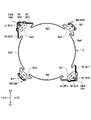
- FIG. 9 is a table showing expansion and contraction states of the shape memory alloy wire SA when each of the five degrees of freedom of movement of the module holder 2 is realized.
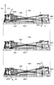
- FIG. 10 shows a top view, a front view, a rear view, a left side view, and a right side view of the module holder 2 and the base member 8 which are connected by the shape memory alloy wire SA.
- FIG. 11 is a top view of the module holder 2 and the base member 8 that translate in the X-axis direction with respect to the base member 8.
- FIG. FIG. 12 is a top view of the module holder 2 and the base member 8 that translate in the Y-axis direction with respect to the base member 8.
- FIG. 13 is a front view of the module holder 2 and the base member 8 rotating around the X-axis (second rotation axis RX2).
- FIG. 14 is a right side view of the module holder 2 and the base member 8 rotating around the Y-axis (third rotation axis RX3).
- FIG. 15 is a top view of the module holder 2 and the base member 8 rotating around the Z-axis (first rotation axis RX1). 10 to 15, for clarity, the module holder 2 has a fine dot pattern and the base member 8 has a coarse dot pattern.
- FIG. 10 shows the state of the module holder 2, base member 8, and shape memory alloy wire SA when the module drive device 101 is in the neutral state (neutral position).
- the module holder 2 which is translatable along the X-axis and the Y-axis with respect to the fixed-side member FB, is positioned in the middle of the movable range in the X-axis direction. and in the middle of the movable range in the Y-axis direction.
- the module holder 2 is positioned at the center of each movable range in the X-axis direction and the Y-axis direction.
- the neutral state of the module driving device 101 is around the X-axis (second rotation axis RX2), the Y-axis (third rotation axis RX3), and the Z-axis (first rotation axis RX1). It means a state in which the rotatable (swingable) module holder 2 is positioned in the middle of the rotatable ranges (rotatable angles) around the respective rotation axes.
- the module holder 2 is positioned at the center of the rotatable range around each of the first to third rotation axes RX1 to RX3.
- the initial state of the module driving device 101 when no current is supplied to the shape memory alloy wires SA may be the neutral state.
- one end (fixed end) of the second wire SA2 is positioned a predetermined distance D1 from the other end (movable end) in a top view from the Z1 side. It is arranged so as to be positioned on the outside (front side (X1 side)).
- One end (fixed end) of the second wire SA2 is the end fixed to the second fixed terminal plate 5F2
- the other end (movable end) of the second wire SA2 is the first movable terminal plate 5M1. is the end that is fixed to the
- the fourth wire SA4 is arranged such that one end (fixed end) thereof is positioned outside (to the left (Y1 side)) the other end (movable end) of the fourth wire SA4 by a predetermined distance D2 when viewed from the top.
- One end (fixed end) of SA6 is positioned outside (rear side (X2 side)) a predetermined distance D3 from the other end (movable end). ) is positioned outside (to the right (Y2 side)) of the other end (movable end) by a predetermined distance D4.
- the first wire SA1, the second wire SA2, the fifth wire SA5, and the sixth wire SA6 are arranged so as to be non-parallel to the Y-axis, and the third wire SA3 and the fourth wire SA3 are arranged to be non-parallel to the Y axis.
- SA4, seventh wire SA7, and eighth wire SA8 are arranged so as to be non-parallel to the X-axis.
- control device can move the module holder 2 along the X-axis or the Y-axis, for example, by contracting a part of the first wire SA1 to the eighth wire SA8 and extending the rest. can be translated.
- the first wire SA1 is arranged so that one end (fixed end) thereof is higher than the other end (movable end) in a front view viewed from the X1 side.
- the second wire SA2 is arranged so that one end (fixed end) is lower than the other end (movable end), and the first wire SA1 and the second wire SA2 are arranged so as to cross each other. It is
- the third wire SA3 is arranged so that one end (fixed end) thereof is higher than the other end (movable end), and the fourth wire SA4 The (fixed end) is positioned lower than the other end (movable end), and the third wire SA3 and the fourth wire SA4 are arranged to cross each other.
- the fifth wire SA5 is arranged so that one end (fixed end) is higher than the other end (movable end), and the sixth wire SA6 is arranged such that one end ( The fixed end) is positioned lower than the other end (movable end), and the fifth wire SA5 and the sixth wire SA6 are arranged to cross each other.
- the seventh wire SA7 is arranged so that one end (fixed end) is higher than the other end (movable end), and the eighth wire SA8 One end (fixed end) is positioned lower than the other end (movable end), and the seventh wire SA7 and the eighth wire SA8 are arranged to cross each other.
- the first wire SA1 to the eighth wire SA8 are all arranged so as to extend obliquely (non-parallel) to the X-axis and the Y-axis.
- first wire SA1 and the second wire SA2 need only be arranged so as to extend obliquely when viewed from the front, and do not need to cross each other when viewed from the front.
- the top view of FIG. 11 is a top view of the module holder 2 and the base member 8 that translate in the X1 direction (forward) with respect to the base member 8, and the center view of FIG. 11 is a top view of the base member 8, and the bottom view of FIG. 11 is a top view of the module holder 2 and the base member 8 that translate in the X2 direction (backward) with respect to the base member 8.
- FIG. 11 is a top view of the module holder 2 and the base member 8 that translate in the X1 direction (forward) with respect to the base member 8
- the center view of FIG. 11 is a top view of the base member 8
- the bottom view of FIG. 11 is a top view of the module holder 2 and the base member 8 that translate in the X2 direction (backward) with respect to the base member 8.
- the controller causes the first wire SA1 and the second wire SA2 to contract relatively small, as shown in the table of FIG.
- the third wire SA3 and fourth wire SA4 are stretched relatively large, the fifth wire SA5 and sixth wire SA6 are stretched relatively small, and the seventh wire SA7 and eighth wire SA8 are contracted relatively large.
- Shrinking the first wire SA1 and the second wire SA2 to a relatively small amount and shrinking the seventh wire SA7 and the eighth wire SA8 to a relatively large amount means that the amount of shrinkage of each of the first wire SA1 and the second wire SA2 is is smaller than the contraction amount of each of the seventh wire SA7 and the eighth wire SA8.
- the control device causes the first wire SA1 and the second wire SA2 to shrink by substantially the same amount and relatively small, and the third wire SA3 and the fourth wire SA4 to stretch by approximately the same amount and relatively large.
- the fifth wire SA5 and the sixth wire SA6 are stretched to a relatively small extent by approximately the same amount of stretching, and the seventh wire SA7 and the eighth wire SA8 are shrunk by approximately the same amount to a relatively large extent.
- the control device expands and contracts each of the first wire SA1 through eighth wire SA8 as described above by individually adjusting the magnitude of the current supplied to each of first wire SA1 through eighth wire SA8.
- the drive unit DM can translate the module holder 2 in the X1 direction (forward) with respect to the base member 8, as indicated by an arrow AR21 in the upper diagram of FIG.
- the controller when the controller translates the module holder 2 in the X2 direction (backward) with respect to the base member 8, the first wire SA1 and the second wire SA2 are relatively small as shown in the table of FIG.
- the third wire SA3 and the fourth wire SA4 are contracted relatively large
- the fifth wire SA5 and the sixth wire SA6 are contracted relatively small
- the seventh wire SA7 and the eighth wire SA8 are contracted relatively large.
- the control device expands and contracts each of the first wire SA1 through eighth wire SA8 as described above by individually adjusting the magnitude of the current supplied to each of first wire SA1 through eighth wire SA8.
- the drive unit DM can translate the module holder 2 in the X2 direction (backward) with respect to the base member 8, as indicated by an arrow AR22 in the lower diagram of FIG.
- the top view of FIG. 12 is a top view of the module holder 2 and the base member 8 that translate in the Y1 direction (leftward) with respect to the base member 8, and the center view of FIG. 12 is the module holder 2 in a neutral state.
- 12 is a top view of the base member 8 and the module holder 2 that translates in the Y2 direction (to the right) with respect to the base member 8.
- the controller stretches the first wire SA1 and the second wire SA2 to a relatively large extent as shown in the table of FIG. , the third wire SA3 and the fourth wire SA4 are shrunk relatively small, the fifth wire SA5 and the sixth wire SA6 are shrunk relatively large, and the seventh wire SA7 and the eighth wire SA8 are stretched relatively small. .
- the control device expands and contracts each of the first wire SA1 through eighth wire SA8 as described above by individually adjusting the magnitude of the current supplied to each of first wire SA1 through eighth wire SA8.
- the drive unit DM can translate the module holder 2 in the Y1 direction (to the left) with respect to the base member 8, as indicated by an arrow AR23 in the upper diagram of FIG.
- the control device when the control device translates the module holder 2 in the Y2 direction (to the right) with respect to the base member 8, the first wire SA1 and the second wire SA2 are relatively shifted as shown in the table of FIG.
- the third wire SA3 and the fourth wire SA4 are stretched relatively little, the fifth wire SA5 and the sixth wire SA6 are stretched relatively greatly, and the seventh wire SA7 and the eighth wire SA8 are relatively stretched. shrink slightly.
- the control device expands and contracts each of the first wire SA1 through eighth wire SA8 as described above by individually adjusting the magnitude of the current supplied to each of first wire SA1 through eighth wire SA8.
- the drive unit DM can translate the module holder 2 in the Y2 direction (to the right) with respect to the base member 8, as indicated by an arrow AR24 in the lower diagram of FIG.
- FIG. 13 is a front view of the module holder 2 and the base member 8 rotating clockwise around the X-axis (second rotation axis RX2) with respect to the base member 8, and the center view of FIG. 13A and 13B are front views of the module holder 2 and the base member 8 in a neutral state, and the lower diagram of FIG. FIG. 2 is a front view of body 2 and base member 8;
- the control device rotates the module holder 2 clockwise around the X axis (second rotation axis RX2) with respect to the base member 8 in a front view
- the first wire SA1 is rotated as shown in the table of FIG.
- the third wire SA3 and the eighth wire SA8 are contracted by approximately the same contraction amount, and the fourth wire SA4 to the seventh wire SA7 are stretched by approximately the same extension amount.
- the control device expands and contracts each of the first wire SA1 through eighth wire SA8 as described above by individually adjusting the magnitude of the current supplied to each of first wire SA1 through eighth wire SA8.
- the drive unit DM rotates the module holder 2 clockwise around the X-axis (second rotation axis RX2) with respect to the base member 8, as indicated by an arrow AR27 in the upper diagram of FIG. can be rotated.
- the control device rotates the module holder 2 counterclockwise around the X axis (second rotation axis RX2) with respect to the base member 8 in a front view, as shown in the table of FIG.
- the first wire SA1 to the third wire SA3 and the eighth wire SA8 are stretched by approximately the same stretching amount, and the fourth wire SA4 to the seventh wire SA7 are contracted by approximately the same shrinking amount.
- the control device expands and contracts each of the first wire SA1 through eighth wire SA8 as described above by individually adjusting the magnitude of the current supplied to each of first wire SA1 through eighth wire SA8.
- the drive unit DM rotates the module holder 2 counterclockwise around the X axis (second rotation axis RX2) with respect to the base member 8, as indicated by an arrow AR28 in the lower diagram of FIG. can be rotated.
- FIG. 14 is a right side view of the module holder 2 rotating clockwise around the Y-axis (third rotation axis RX3) with respect to the base member 8 and the base member 8, and the center view of FIG. 14 is a right side view of the module holder 2 and the base member 8 in a neutral state, and the lower view of FIG. 4 is a right side view of the module holder 2 and the base member 8.
- FIG. 14 is a right side view of the module holder 2 rotating clockwise around the Y-axis (third rotation axis RX3) with respect to the base member 8 and the base member 8, and the center view of FIG. 14 is a right side view of the module holder 2 and the base member 8 in a neutral state, and the lower view of FIG. 4 is a right side view of the module holder 2 and the base member 8.
- the control device rotates the module holder 2 clockwise around the Y-axis (third rotation axis RX3) with respect to the base member 8 in the right side view, the first wire SA1, third wire SA3, fourth wire SA4, and sixth wire SA6 are shrunk substantially by the same amount, and second wire SA2, fifth wire SA5, seventh wire SA7, and eighth wire SA8 are substantially shrunk. Stretch with the same stretch amount.
- the control device expands and contracts each of the first wire SA1 through eighth wire SA8 as described above by individually adjusting the magnitude of the current supplied to each of first wire SA1 through eighth wire SA8.
- the drive unit DM rotates the module holder 2 clockwise around the Y-axis (third rotation axis RX3) with respect to the base member 8, as indicated by an arrow AR29 in the upper diagram of FIG. can be rotated.
- the controller rotates the module holder 2 as shown in the table of FIG. , the first wire SA1, the third wire SA3, the fourth wire SA4, and the sixth wire SA6 are stretched by substantially the same amount of stretching, and the second wire SA2, the fifth wire SA5, the seventh wire SA7, and the eighth The wire SA8 is shrunk by approximately the same amount of shrinkage.
- the control device expands and contracts each of the first wire SA1 through eighth wire SA8 as described above by individually adjusting the magnitude of the current supplied to each of first wire SA1 through eighth wire SA8.
- the drive unit DM rotates the module holder 2 counterclockwise around the Y-axis (third rotation axis RX3) with respect to the base member 8, as indicated by an arrow AR30 in the lower diagram of FIG. can be rotated.
- the first wire SA1 to the eighth wire SA8, which expand and contract so as to move the module holder 2 with respect to the base member 8 so that the optical axis OA of the lens body LS is tilted serve as a first drive unit DM.
- it can be oscillated around a second oscillating axis (third rotational axis RX3) that intersects the optical axis direction and is perpendicular to the first oscillating axis (second rotational axis RX2).
- the top view of FIG. 15 is a top view of the module holder 2 rotating clockwise around the Z-axis (first rotation axis RX1) with respect to the base member 8 and the base member 8.
- the center view of FIG. 15 is a top view of the module holder 2 and the base member 8 in a neutral state
- the lower view of FIG. FIG. 4 is a top view of the body 2 and the base member 8;
- the control device rotates the module holder 2 clockwise around the Z-axis (first rotation axis RX1) with respect to the base member 8 in top view
- the first wire SA1 is rotated as shown in the table of FIG.
- the second wire SA2 the fifth wire SA5, and the sixth wire SA6 are stretched by approximately the same amount of stretching
- the third wire SA3, the fourth wire SA4, the seventh wire SA7, and the eighth wire SA8 are stretched by approximately the same amount.
- the control device expands and contracts each of the first wire SA1 through eighth wire SA8 as described above by individually adjusting the magnitude of the current supplied to each of first wire SA1 through eighth wire SA8.
- the drive unit DM rotates the module holder 2 clockwise around the Z-axis (first rotation axis RX1) with respect to the base member 8, as indicated by an arrow AR31 in the upper diagram of FIG. can be rotated.
- the control device rotates the module holder 2 counterclockwise around the Z-axis (first rotation axis RX1) with respect to the base member 8 in top view, as shown in the table of FIG.
- the first wire SA1, the second wire SA2, the fifth wire SA5, and the sixth wire SA6 are contracted by substantially the same contraction amount, and the third wire SA3, the fourth wire SA4, the seventh wire SA7, and the eighth wire are contracted.
- SA8 is extended by approximately the same amount of extension.
- the control device expands and contracts each of the first wire SA1 through eighth wire SA8 as described above by individually adjusting the magnitude of the current supplied to each of first wire SA1 through eighth wire SA8.
- the drive unit DM rotates the module holder 2 counterclockwise around the Z axis (first rotation axis RX1) with respect to the base member 8, as indicated by an arrow AR32 in the lower diagram of FIG. can be rotated.
- a second driving section DM2 (see FIG. 2) is configured as the section DM. That is, in the present embodiment, the plurality of shape memory alloy wires SA (the first wires SA1 to the eighth wires SA8) forming the first drive section DM1 are replaced by the plurality of shape memory alloy wires SA forming the second drive section DM2. (first wire SA1 to eighth wire SA8).
- the driving unit DM including the first driving unit DM1 and the second driving unit DM2 moves in the direction (X-axis direction and Y-axis direction) intersecting the optical axis direction of the module holder 2. and swings the module holder 2 around swing axes (second rotation axis RX2 and third rotation axis RX3) intersecting the optical axis direction as shown in FIGS. As shown in FIG. 15, the module holder 2 can be rotated around the optical axis OA.
- the module holder 2 can realize movement with 5 degrees of freedom. Each of these five degrees of freedom of movement is realized by individually adjusting the current supplied to each of the first wire SA1 to the eighth wire SA8.
- the movement of the module holder 2 may be achieved by combining a plurality of movements out of the five degrees of freedom.
- the module holder 2 moves when the corresponding shape memory alloy wire SA is contracted by applying current to one or more of the first wire SA1 to the eighth wire SA8. By the movement, another one or more of the first wire SA1 to the eighth wire SA8 are stretched, thereby realizing the stretching of the shape memory alloy wire SA.
- the lens body LS in the camera module MD held by the module holder 2 can move with 6 degrees of freedom. It is possible to realize a degree of movement. That is, the combination of the driving section DM in the module driving device 101 and the driving section in the camera module MD can realize the movement of the lens body LS with six degrees of freedom.
- the lens body LS in the camera module MD held by the module holding body 2 can achieve 6 degrees of freedom of movement.
- the drive unit DM in the module drive device 101 is configured to be able to rotate around the first rotation axis RX1, around the second rotation axis RX2, and around the third rotation axis RX3. It is good if it is. That is, the drive unit DM may be configured not to use translation along the second rotation axis RX2 and translation along the third rotation axis RX3.
- the drive unit DM can, in principle, move the module holder 2 with 6 degrees of freedom, but should not use translation in the Z-axis direction (optical axis direction). It is configured. This is because the focal length (the distance between the center point of the lens body LS and the image sensor IS) cannot be changed even if the module holding body 2 is translated in the optical axis direction. Therefore, in the above-described embodiment, it is not necessary to secure a space in the housing HS that is required when the module holder 2 is translated in the optical axis direction. Therefore, such a space-free configuration can be formed to have a smaller height dimension than a configuration that can utilize the translation of the module holder 2 in the Z-axis direction.
- the configuration that does not use the translation of the module holder 2 in the X-axis direction can omit the space required for translating the module holder 2 in the X-axis direction. It may be formed to have a smaller width dimension in the X-axis direction than a configuration formed to utilize translation. The same applies to a configuration that does not use translation of the module holder 2 in the Y-axis direction.
- the five-degree-of-freedom movement of the movable-side member MB as described above is detected by a motion detector (not shown).
- the motion detector includes, for example, at least three magnets attached to the movable side member MB such as the module holder 2, and at least three magnetic sensors attached to the fixed side member FB such as the base member 8 or the flexible substrate 3. Consists of
- the magnetic sensor is configured to detect the position of the movable side member MB by detecting the position of the magnet.
- the magnetic sensor is configured to detect the position of the movable member MB using a Hall element.
- the magnetic sensor is a Giant Magneto Resistive effect (GMR) element that can detect the magnetic field generated by a magnet, a Semiconductor Magneto Resistive (SMR) element, an Anisotropic Magneto Resistive
- the position of the movable side member MB may be detected using a magnetic resistance element such as an AMR (Tunnel Magneto Resistive: TMR) element or a Tunnel Magneto Resistive (TMR) element.
- AMR Unnel Magneto Resistive: TMR
- TMR Tunnel Magneto Resistive
- FIG. 16 is an exploded perspective view of the camera module MD. 16, for clarity, the cover member 4x (see FIG. 1B), the circuit board 7 (see FIG. 1B), the lens body LS (see FIG. 1B), and the image sensor IS (see FIG. 1B). ) are omitted.
- the camera module MD includes a lens holder 2x, a module-side metal member 5x, a leaf spring 6x, a module-side base member 8x, and module-side shape memory alloy wires SAx.
- the lens holder 2x is formed by injection molding synthetic resin such as liquid crystal polymer (LCP). Specifically, as shown in FIG. 16, the lens holder 2x is formed with a tubular portion 12x formed so as to extend along the optical axis OA, and a tubular portion 12x formed so as to protrude radially outward from the tubular portion 12x. and a movable-side pedestal portion 2Dx and a projecting portion 2Sx. In the example shown in FIG. 16, a spiral groove is formed on the inner peripheral surface of the cylindrical portion 12x so that the adhesive spreads between the upper half of the inner peripheral surface and the lens body LS (see FIG. 1B). ing.
- LCP liquid crystal polymer
- the movable-side pedestal portion 2Dx includes a first movable-side pedestal portion 2D1x and a second movable-side pedestal portion 2D2x.
- the first movable-side pedestal portion 2D1x and the second movable-side pedestal portion 2D2x are arranged so as to extend radially outward in opposite directions to each other with the optical axis OA interposed therebetween.
- the projecting portion 2Sx includes a first projecting portion 2S1x and a second projecting portion 2S2x.
- the first projecting portion 2S1x and the second projecting portion 2S2x are arranged so as to extend radially outward in opposite directions to each other with the optical axis OA interposed therebetween.
- the movable-side pedestal portion 2Dx and the projecting portion 2Sx are arranged so as to correspond to the four corners of the lens holding body 2x having a substantially rectangular frame-like outer shape when viewed from above, and are arranged alternately. are arranged as A part of the plate spring 6x is placed and fixed on each of the two movable-side pedestals 2Dx.
- the leaf spring 6x is configured to support the lens holder 2x movably in a direction parallel to the optical axis OA with respect to the module-side fixing member FBx (module-side base member 8x).
- the leaf spring 6x is made of a metal plate whose main material is, for example, a copper alloy, a titanium-copper alloy (titanium-copper), or a copper-nickel alloy (nickel-tin-copper).
- the leaf springs 6x include a first leaf spring 6Ax and a second leaf spring 6Bx.
- the module-side base member 8x is formed by injection molding using synthetic resin such as liquid crystal polymer (LCP).
- LCP liquid crystal polymer
- the module-side base member 8x similarly to the base member 8 (see FIG. 6), has a substantially rectangular frame-shaped outline when viewed from above, and has an opening 8Kx in the center.
- the module-side base member 8x has a rectangular annular base arranged to surround the circular opening 8Kx.
- the base has four side portions 8Ex (first side portion 8E1x to fourth side portion 8E4x).
- the module-side base member 8x is integrated with the cover member 4x with an adhesive or the like, and together with the cover member 4x constitutes the housing of the camera module MD.
- the circuit board 7 is fixed to the lower surface of the module-side base member 8x with an adhesive.
- a frame-shaped spacer formed so as to surround the imaging element IS may be provided between the circuit board 7 and the module-side base member 8x.
- the leaf spring 6x is configured to connect a movable side pedestal portion 2Dx formed on the lens holder 2x and a fixed side pedestal portion 8Dx formed on the module side base member 8x.
- the fixed-side pedestal portion 8Dx is a portion that protrudes upward from the base portion of the module-side base member 8x, and includes a first fixed-side pedestal portion 8D1x and a second fixed-side pedestal portion 8D2x.
- the first plate spring 6Ax includes a first movable-side pedestal portion 2D1x formed on the lens holder 2x, and a first fixed-side pedestal portion 8D1x and a second fixed-side pedestal portion 8D1x formed on the module-side base member 8x. It is configured to connect to each of the side pedestals 8D2x.
- the second leaf spring 6Bx includes a second movable side seat portion 2D2x formed on the lens holder 2x, and a first fixed side seat portion 8D1x and a second fixed side seat portion 8D1x formed on the module side base member 8x. 8D2x are configured to be connected to each other.
- the module-side metal member 5x is configured so that the ends of the module-side shape memory alloy wires SAx are fixed.
- the module-side metal member 5x is made of non-magnetic metal and includes a module-side fixed metal member 5Fx and a module-side movable metal member 5Mx.
- the module-side fixed metal member 5Fx is configured to be fixed to the fixed-side pedestal portion 8Dx of the module-side base member 8x.
- the module-side movable metal member 5Mx is configured to be fixed to the movable-side pedestal portion 2Dx of the lens holder 2x.
- the module-side fixed metal member 5Fx is also called a fixed-side terminal plate and includes a ninth fixed-side terminal plate 5F9 to a sixteenth fixed-side terminal plate 5F16.
- the module-side movable metal member 5Mx is also called a movable-side terminal plate, and includes a third movable-side terminal plate 5M3 to a sixth movable-side terminal plate 5M6.
- the first plate spring 6Ax has a first portion 6A1x fixed to the first fixed side seat portion 8D1x of the module side base member 8x and a second portion fixed to the second fixed side seat portion 8D2x of the module side base member 8x. 6A2x and a third portion 6A3x fixed to the first movable side pedestal portion 2D1x of the lens holder 2x.
- the first portion 6A1x is connected to a conductive member (not shown) embedded in the module-side base member 8x by laser welding or the like, and the third portion 6A3x is connected to the third movable side terminal plate 5M3 and the fourth movable side terminal plate 5M3 by soldering or the like. It is connected to each terminal plate 5M4.
- the second leaf spring 6Bx is fixed to the first portion 6B1x fixed to the first fixed side seat portion 8D1x of the module side base member 8x and to the second fixed side seat portion 8D2x of the module side base member 8x. It has a second portion 6B2x and a third portion 6B3x fixed to the second movable side pedestal portion 2D2x of the lens holder 2x.
- the second portion 6B2x is connected to a conductive member (not shown) embedded in the module-side base member 8x by laser welding or the like. It is connected to each terminal plate 5M6.
- the module-side shape-memory alloy wire SAx is another example of a shape-memory actuator. Similar to the shape-memory alloy wire SA (see FIG. 2), the temperature rises when current flows, and according to the temperature rise, Shrink. Specifically, the module-side shape memory alloy wire SAx extends along the inner surface of the outer peripheral wall portion of the cover member 4x, and can movably support the module-side movable member MBx with respect to the module-side fixed member FBx. is configured as In the example shown in FIG.
- the module-side shape-memory alloy wires SAx include eight shape-memory alloy wires (9th wire SA9 to 16th wire SA16), and are attached to the module-side base member 8x as the module-side fixing member FBx. On the other hand, it is configured to movably support a lens holder 2x as a module-side movable member MBx. As shown in FIG. 16, each of the ninth wire SA9 to the sixteenth wire SA16 has one end fixed to the module-side stationary metal member 5Fx by crimping or welding, and the other end being crimped or welded to move the module side. It is fixed to the metal member 5Mx.
- Each of the ninth fixed side terminal plate 5F9 to the sixteenth fixed side terminal plate 5F16 that fixes one end of each of the ninth wire SA9 to the sixteenth wire SA16 is a corresponding terminal member embedded in the module side base member 8x. It is electrically connected to a corresponding conductive pattern formed on the circuit board 7 via (a conductive member). Further, each of the third movable side terminal plate 5M3 to sixth movable side terminal plate 5M6 fixing the other end of each of the ninth wire SA9 to sixteenth wire SA16 has a plate spring 6x (first plate spring 6Ax and second plate spring 6Ax).
- the camera module MD is configured to be able to receive currents flowing through the ninth wire SA9 to the sixteenth wire SA16 via the flexible substrate 3 and the circuit substrate 7, respectively.
- the module-side shape memory alloy wire SAx constitutes the module-side drive section DMx.
- the module-side drive section DMx can move the lens holder 2x with respect to the module-side base member 8x by utilizing contraction of the module-side shape memory alloy wire SAx. Note that when one or more of the ninth wire SA9 to sixteenth wire SA16 contracts, the lens holder 2x moves, and another one or more of the module-side shape memory alloy wires SAx are elongated by the movement. configured to be
- the module-side drive unit DMx is theoretically configured so that the module-side movable member MBx can move with six degrees of freedom.
- the movements of the six degrees of freedom are translation in a first direction (Z-axis direction) that is the direction of the optical axis, translation in a second direction (X-axis direction) perpendicular to the first direction (Z-axis direction), Translation in a third direction (Y-axis direction) perpendicular to each of the two directions, rotation about a first direction (Z-axis direction), rotation about a second direction (X-axis direction), and a third direction ( Y-axis direction).
- the first direction (Z-axis direction) is parallel to the first rotation axis RX1 that coincides with the optical axis OA of the lens body LS, and the second direction (X-axis direction) is parallel to the second rotation axis RX2.
- the third direction (Y-axis direction) is parallel to the third rotation axis RX3.
- the second rotation axis RX2 is also called a first swing axis
- the third rotation axis RX3 is also called a second swing axis.
- the module-side driving section DMx is configured not to use rotation around the first direction (Z-axis direction).
- FIG. 17 is a table showing expansion and contraction states of the module-side shape memory alloy wire SAx when realizing each of the five degrees of freedom of movement of the lens holder 2x.
- FIG. 17 differs from the table shown in FIG. 9 in that it does not have a column for "Z-axis rotation” but has a column for "Z-axis direction translation", but in other respects it is the same as the table shown in FIG. be.
- the ninth wire SA9 to sixteenth wire SA16 in FIG. 17 correspond to the first wire SA1 to eighth wire SA8 in FIG.
- the state of the module-side shape memory alloy wire SAx when the lens holder 2x is translated in the Z-axis direction with respect to the module-side base member 8x will be described below.
- the control device When the control device translates the lens holder 2x in the Z1 direction (upward) with respect to the module-side base member 8x, as shown in the table of FIG. , and fifteenth wire SA15, and tenth wire SA10, twelfth wire SA12, fourteenth wire SA14, and sixteenth wire SA16 are stretched.
- the controller expands and contracts each of the ninth wire SA9 to sixteenth wire SA16 by individually adjusting the magnitude of the current supplied to each of the ninth wire SA9 to sixteenth wire SA16.
- the module-side driving section DMx can translate the lens holder 2x in the Z1 direction (upward) with respect to the module-side base member 8x.
- the control device translates the lens holder 2x in the Z2 direction (downward) with respect to the module-side base member 8x, as shown in the table of FIG.
- the 13th wire SA13 and the 15th wire SA15 are stretched by approximately the same amount of stretching, and the 10th wire SA10, the 12th wire SA12, the 14th wire SA14 and the 16th wire SA16 are contracted by approximately the same amount of contraction.
- the controller expands and contracts each of the ninth wire SA9 to sixteenth wire SA16 by individually adjusting the magnitude of the current supplied to each of the ninth wire SA9 to sixteenth wire SA16.
- the module-side driving section DMx can translate the lens holder 2x in the Z2 direction (downward) with respect to the module-side base member 8x.
- the module drive device 101 can hold an optical module (camera module MD) having a fixed side member FB, a lens body LS, and an image sensor IS, as shown in FIG. a module holding body 2, a first driving section DM1 for moving the module holding body 2 with respect to the fixed side member FB so that the optical axis OA of the lens body LS is tilted, and a first driving section DM1 for rotating the module holding body 2 around the optical axis OA. and a second driving part DM2 for rotating the module holder 2 with respect to the fixed side member FB.
- an optical module camera module MD
- FIG. a module holding body 2
- a first driving section DM1 for moving the module holding body 2 with respect to the fixed side member FB so that the optical axis OA of the lens body LS is tilted
- a first driving section DM1 for rotating the module holding body 2 around the optical axis OA.
- a second driving part DM2 for rotating the module holder 2 with respect to the
- the first drive part DM1 includes a plurality of shape memory alloy wires SA provided between a movable member MB including the module holder 2 and a fixed member FB.
- the second drive part DM2 includes a plurality of shape memory alloy wires SA provided between the movable member MB and the fixed member FB.
- this configuration can suppress an increase in the size of the module driving device 101 and, for example, can realize a smaller size than a device using a voice coil motor for moving the module holder 2 . Moreover, this configuration can realize weight reduction of the module driving device 101 . In addition, since this configuration does not use a voice coil motor for moving the module holder 2, even if a device using a voice coil motor is arranged next to the device, the module driving device 101 will It is possible to suppress magnetic interference between
- this configuration allows the module holder 2 to rotate around the optical axis OA of the lens body LS. It is possible to suppress the influence on the image due to the camera shake that causes the rotation about the axis of .
- this configuration can move the module holder 2 so that the optical axis OA of the lens body LS is tilted. You can correct camera shake like tilting. For example, this configuration can realize camera shake correction even when the camera module MD does not have a camera shake correction function.
- the plurality of shape memory alloy wires SA (the first wires SA1 to the eighth wires SA8) forming the first drive section DM1 are connected to the plurality of shape memory alloy wires SA forming the second drive section DM2. It may also serve as SA (first wire SA1 to eighth wire SA8).
- the first driving section DM1 and the second driving section DM2 may constitute a driving section DM that moves the module holder 2 with respect to the fixed side member FB. This configuration has the effect of reducing the number of parts and thus realizing the miniaturization of the module drive device 101 .
- the first drive unit DM1 swings the module holder 2 around the first swing axis (second rotation axis RX2) intersecting the optical axis direction as shown in FIG.
- it may be oscillated around a second oscillating axis (third rotation axis RX3) having an axial direction that intersects the optical axis direction and is perpendicular to the axial direction of the first oscillating axis.
- the first swing shaft and the second swing shaft do not have to be perpendicular to each other. good. That is, the first swing shaft and the second swing shaft may be in a twisted relationship.
- the module holder 2 can be oscillated about two oscillating axes perpendicular to each other by the first driving unit DM1 housed in a limited space in the housing HS, so that the module can be driven.
- the effect that the space efficiency of the device 101 can be improved and the miniaturization of the module driving device 101 can be achieved is brought about.
- the driving section DM including the first driving section DM1 and the second driving section DM2 may be configured to move the module holder 2 in a direction intersecting the optical axis direction.
- This configuration can correct camera shake in the front-rear direction (X-axis direction) and left-right direction (Y-axis direction) when shooting with a device such as a smartphone in which the module drive device 101 is mounted.
- this configuration can realize camera shake correction even when the camera module MD does not have a camera shake correction function.
- the plurality of shape memory alloy wires SA are arranged in the module holder 2 when viewed from above along the optical axis direction (the axial direction of the first rotation axis RX1).
- a sixth wire SA6 arranged in the .
- each of the first wire SA1, the second wire SA2, the fifth wire SA5, and the sixth wire SA6 is fixed to the fixed side member FB (base member 8), and the other end is fixed to the movable side member MB (module It may be fixed to the holder 2).
- the first wire SA1, the second wire SA2, the fifth wire SA5, and the sixth wire SA6 arranged in a limited space inside the housing HS connect the module holder 2 to the fixed member FB. can be efficiently moved with 6 degrees of freedom.
- the plurality of shape memory alloy wires SA are arranged in the module holder 2 when viewed from above along the optical axis direction (the axial direction of the first rotation axis RX1).
- a third wire SA3 and a seventh wire SA7 which are spaced apart in a second direction (Y-axis direction) perpendicular to the first direction (X-axis direction) with the ) in a side view (left side view), the fourth wire SA4 arranged to intersect with the third wire SA3 and a side view ( In a right side view), an eighth wire SA8 arranged to cross the seventh wire SA7 may be further included.
- Each of the third wire SA3, the fourth wire SA4, the seventh wire SA7, and the eighth wire SA8 has one end fixed to the fixed side member FB (base member 8) and the other end fixed to the movable side member MB (module It may be fixed to the holder 2).
- the first wire SA1 to eighth wire SA8 arranged in the limited space inside the housing HS allow the module holder 2 to be moved more efficiently with six degrees of freedom with respect to the fixed side member FB. bring about the effect of being able to
- the stationary member FB may have eight first metal members (the first stationary terminal plate 5F1 to the eighth stationary terminal plate 5F8).
- one end of each of the eight shape memory alloy wires SA (first wire SA1 to eighth wire SA8) may be individually connected to the corresponding first metal member.
- one end of the first wire SA1 is connected to the first fixed terminal plate 5F1
- one end of the second wire SA2 is connected to the second fixed terminal plate 5F2
- the second wire SA1 is connected to the first fixed terminal plate 5F1.
- One end of the 3-wire SA3 is connected to the third fixed terminal plate 5F3, one end of the fourth wire SA4 is connected to the fourth fixed-side terminal plate 5F4, and one end of the fifth wire SA5 is connected to the fifth fixed-side terminal plate 5F5.
- One end of the sixth wire SA6 is connected to the sixth fixed side terminal plate 5F6, one end of the seventh wire SA7 is connected to the seventh fixed side terminal plate 5F7, and one end of the eighth wire SA8 is connected to the eighth fixed side terminal plate 5F7. It is connected to the terminal plate 5F8.
- This configuration has the effect of facilitating the securing of conductive paths for supplying currents individually to the eight shape memory alloy wires SA.
- the other ends of at least four shape memory alloy wires SA out of the eight shape memory alloy wires SA are electrically connected to each other via conductors provided on the movable side member MB. You may have In this configuration, the other ends of at least four shape memory alloy wires SA out of eight shape memory alloy wires SA are connected to a common potential. Therefore, this configuration brings about the effect of further facilitating the securing of conductive paths for allowing current to be individually supplied to each of the eight shape memory alloy wires SA.
- the conductors are composed of a second metal member (movable side metal member 5M) to which the other ends of at least four shape memory alloy wires SA are connected, a movable side member MB and a fixed side member MB.
- An elastically deformable elastic metal member 6 connecting with the member FB may be included.
- the fixed-side member FB may have a columnar portion (fixed-side pedestal portion 8D) in which the third metal member (conductive member CM) is embedded. Then, as shown in FIG.
- the fixing portions (the second fixing portion 6e2 and the fourth fixing portion 6e4) of the elastic metal member 6 are connected to the second metal member (the movable side metal member 5M), and the third metal member ( Another fixing portion (the first fixing portion 6e1 and the third fixing portion 6e3) of the elastic metal member 6 may be connected to the conductive member CM).
- the elastic metal member 6 may be a leaf spring. This configuration brings about an effect that it becomes easier to secure a conductive path for supplying an electric current to each of the eight shape memory alloy wires SA.
- the other ends of the eight shape memory alloy wires SA are configured to be electrically connected to each other through the movable metal member 5M, the elastic metal member 6, and the conductive member CM. .
- the other ends of the first to fourth wires SA1 to SA4 are connected to the first movable terminal plate 5M1, the elastic metal member 6, the first conductive member CM1 or the second conductive member CM1. It is connected to the ground terminal via the member CM2.
- the other end of each of the fifth wire SA5 to the eighth wire SA8 is connected to the ground terminal through the second movable terminal plate 5M2, the elastic metal member 6, and the first conductive member CM1 or the second conductive member CM2.
- the first fixing portion 6e1 of the elastic metal member 6 is welded to the first joint surface portion CP1 (see the central view of FIG. 6) of the first conductive member CM1, and the third fixing portion 6e3 of the elastic metal member 6 are welded to the second joint surface portion CP2 (see the central view of FIG. 6) of the second conductive member CM2.
- the first connection part ED1 (see the central view of FIG. 6) of the first conductive member CM1 is soldered to the ninth conductive pattern PT9 (see FIG. 2) of the flexible substrate 3, and the second conductive member
- the second connection part ED2 of CM2 is soldered to the tenth conductive pattern PT10 of the flexible substrate 3 (see FIG. 2). Both the ninth conductive pattern PT9 and the tenth conductive pattern PT10 are connected to a ground terminal (not shown).
- the fixed side member FB may have a housing HS (cover member 4) having a shape (for example, a substantially rectangular shape) having at least four corners 4C when viewed from above.
- the housing HS (cover member 4) has a first corner 4C1 and a third corner 4C3 located on one diagonal line and a second corner located on the other diagonal line. It may have a portion 4C2 and a fourth corner portion 4C4.
- One end of each of the eight shape-memory alloy wires SA is a base member that functions as a fixed-side wire support portion for the fixed-side member FB arranged to face the first corner portion 4C1 or the third corner portion 4C3.
- each of the eight shape memory alloy wires SA is arranged to face the second corner portion 4C2 or the fourth corner portion 4C4 of the movable side member MB. It may be supported by the movable-side pedestal portion 2D of the module holder 2 that functions as the movable-side wire support portion.
- This configuration brings about the effect of further suppressing the increase in size of the module driving device 101 .
- this configuration brings about an effect that further weight reduction of the module drive device 101 can be achieved.
- the housing HS may be configured to have another shape such as a substantially hexagonal shape or a substantially octagonal shape when viewed from above.
- the imaging element IS may be mounted on the circuit board 7 as the first printed wiring board.
- the circuit board 7 may be fixed to the module holder 2 and connected to the flexible board 3 as a second flexible printed wiring board.
- the circuit board 7 may be configured to be thicker than the flexible board 3 . This configuration brings about an effect that the imaging device IS can be easily integrated with the module holder 2 .
- the image pickup device IS may be provided with an IR cut filter.
- the camera module MD may have a circuit board 7 as a first printed wiring board on which the imaging element IS is mounted, as shown in FIG. 1B.
- the fixed-side member FB may have a flexible substrate 3 as a flexible second printed circuit board.
- the flexible board 3 may be connected to the circuit board 7 and eight first metal members (first fixed terminal plate 5F1 to eighth fixed terminal plate 5F8).
- the first printed wiring board (circuit board 7) and the eight first metal members (first fixed side terminal plate 5F1 to eighth fixed side terminal plate 5F8) are all connected to the second printed wiring board (flexible It is connected to the substrate 3).
- the circuit board 7 is connected to the inner portion 3i of the flexible board 3 (see FIG. 2).
- the first connecting portion CT1 (see FIG. 7A) of the first fixed-side terminal plate 5F1 is connected to the first conductive pattern PT1 (see FIG. 2) formed on the outer portion 3e of the flexible substrate 3. be.
- the second connection portion CT2 is connected to the second conductive pattern PT2
- the third connection portion CT3 is connected to the third conductive pattern PT3
- the fourth connection portion CT4 is connected to the fourth conductive pattern PT4
- the fifth connection portion CT4 is connected to the fourth conductive pattern PT4.
- connection portion CT5 is connected to the fifth conductive pattern PT5
- the sixth connection portion CT6 is connected to the sixth conductive pattern PT6
- the seventh connection portion CT7 is connected to the seventh conductive pattern PT7
- the eighth connection portion CT8 is connected to the third conductive pattern PT6. 8 is connected to the conductive pattern PT8. Therefore, this configuration has the effect of facilitating connection with an external device.
- the optical device (imaging device) according to the embodiment of the present invention includes the module driving device 101 described above and an optical module (camera module MD) held by the module holder 2. have.
- this configuration can suppress the increase in size of the optical device, and can achieve a smaller size than, for example, a device using a voice coil motor for moving the optical module (camera module MD).
- this configuration can realize weight reduction of the optical device.
- this configuration does not use a voice coil motor to move the optical module (camera module MD), even if a device using a voice coil motor is placed next to the device, the device and the optical device cannot be separated from each other. can suppress magnetic interference between
- the optical module includes a module-side fixing member FBx (module-side base member 8x) that moves together with the module holder 2 (see FIG. 2), and a lens body LS (see FIG. 2). ), and a module-side driving section DMx for moving the lens holding body 2x with respect to the module-side fixing member FBx (module-side base member 8x).
- the module-side drive unit DMx accommodated in a limited space in the housing of the camera module MD can move the lens holder 2x with respect to the module-side fixing member FBx (module-side base member 8x). Therefore, it is possible to improve the space efficiency of the camera module MD, and eventually, it is possible to realize the miniaturization of the camera module MD and the optical device.
- the module-side driving unit DMx includes a plurality of module-side shape memory modules provided between the module-side movable member MBx including the lens holder 2x and the module-side fixed member FBx (module-side base member 8x). It may be configured to include an alloy wire SAx.
- the optical device may include the module driving device 101 described above and an optical module held by the module holding body 2 .
- the optical module includes a module-side fixing member FBx (module-side base member 8x) that moves together with the module holder 2, a lens holder 2x that holds the lens body LS (see FIG. 2), and a module-side fixing member. and a module-side driving section DMx for moving the lens holder 2x with respect to FBx (module-side base member 8x).
- the module-side driving portion DMx includes a plurality of module-side shape memory alloy wires SAx provided between the module-side movable member MBx including the lens holder 2x and the module-side fixed member FBx (module-side base member 8x).
- the plurality of module-side shape memory alloy wires SAx are spaced apart in the axial direction of the first swing shaft (second rotation shaft RX2) with the lens holder 2x interposed therebetween in a top view along the optical axis direction.
- a 12th wire SA12 arranged to cross the 11th wire SA11 in a side view (left side view) along the axial direction of the second swing shaft (third rotation axis RX3);
- a 14th wire SA14 arranged to intersect with a 13th wire SA13, and a second swing axis
- a sixteenth wire SA16 arranged to cross the fifteenth wire SA15 in a side view (right side view) along the axial direction of the (third rotation axis RX3).
- each of the ninth wire SA9 to the sixteenth wire SA16 is fixed to the module-side fixed member FBx (the module-side fixed metal member 5Fx fixed to the module-side base member 8x), and the other end is fixed to the module-side movable member. It may be fixed to MBx (module side movable metal member 5Mx fixed to lens holder 2x).
- the module-side movable member MBx is attached to the module-side fixed member FBx (module-side base member 8x) by the ninth wire SA9 to sixteenth wire SA16 arranged in a limited space in the housing of the camera module MD. can be moved more efficiently in multiple degrees of freedom (eg, 5 degrees of freedom).
- the elastic metal member 6 is composed of one part, but it may be composed of two parts.
- the elastic metal member 6 may be divided into a first elastic metal member and a second elastic metal member at each of the central portion of the first fixing portion 6e1 and the central portion of the third fixing portion 6e3. good.
- the first elastic metal member may be configured to be connected to the first conductive member CM1 and not connected to the second conductive member CM2.
- the second elastic metal member may be configured to be connected to the second conductive member CM2 and not to be connected to the first conductive member CM1.
- the position of the movable-side member MB is detected based on the output of the magnetic sensor, but it may be detected based on the output of a sensor that detects the resistance value of the shape memory alloy wire SA. .
- the fixed-side metal member 5F is fixed to the base member 8 with an adhesive, but it may be embedded in the base member 8, and the conductive pattern formed on the surface of the base member 8 may be fixed.
- the movable-side metal member 5M is fixed to the module holder 2 with an adhesive, but may be embedded in the module holder 2 and may be a conductive pattern formed on the surface of the module holder 2.
- the cover member 4x of the lens driving device LD that constitutes the camera module MD is a separate member from the module holder 2, but the cover member 4x and the module holder 2 are integrally formed.
- the cover member 4x constitutes a module holder, and the optical module held by this module holder may be the camera module MD without the cover member 4x.
- the movable-side member MB is mainly composed of the module holder 2, but the movable-side member MB may be composed of a combination of a plurality of mutually movable members.
- Corner part 4C1 First corner part 4C2... Second corner part 4C3... Third corner part 4C4... Fourth corner 4K... Opening 5... Metal member 5F... Fixed side metal member 5F1... First fixed side terminal plate 5F2... Second fixed side terminal plate 5F3... ⁇ Third fixed side terminal plate 5F4... Fourth fixed side terminal plate 5F5... Fifth fixed side terminal plate 5F6... Sixth fixed side terminal plate 5F7...
- first connection part ED2 ... ⁇ Second connecting part FB...Fixed side member FBx...Module side fixed member HS...Housing IS...Image sensor J1 to J4...Holding part LD...Lens drive unit LS... ⁇ Lens body MB... Movable side member MBx... Module side movable member MD... Camera module OA... Optical axis PT... Conductive pattern PT1... First conductive pattern PT2... Second Conductive pattern PT3... Third conductive pattern PT4... Fourth conductive pattern PT5... Fifth conductive pattern PT6... Sixth conductive pattern PT7... Seventh conductive pattern PT8... Eighth conductive pattern PT9... ⁇ Ninth conductive pattern PT10...
Landscapes
- Physics & Mathematics (AREA)
- General Physics & Mathematics (AREA)
- Optics & Photonics (AREA)
- Engineering & Computer Science (AREA)
- Multimedia (AREA)
- Signal Processing (AREA)
- Lens Barrels (AREA)
- Adjustment Of Camera Lenses (AREA)
- Studio Devices (AREA)
Priority Applications (2)
| Application Number | Priority Date | Filing Date | Title |
|---|---|---|---|
| JP2023514523A JP7556640B2 (ja) | 2021-04-14 | 2022-03-14 | モジュール駆動装置及び光学装置 |
| CN202280028365.8A CN117203581A (zh) | 2021-04-14 | 2022-03-14 | 模块驱动装置以及光学装置 |
Applications Claiming Priority (2)
| Application Number | Priority Date | Filing Date | Title |
|---|---|---|---|
| JP2021-068544 | 2021-04-14 | ||
| JP2021068544 | 2021-04-14 |
Publications (1)
| Publication Number | Publication Date |
|---|---|
| WO2022219984A1 true WO2022219984A1 (ja) | 2022-10-20 |
Family
ID=83640309
Family Applications (1)
| Application Number | Title | Priority Date | Filing Date |
|---|---|---|---|
| PCT/JP2022/011224 Ceased WO2022219984A1 (ja) | 2021-04-14 | 2022-03-14 | モジュール駆動装置及び光学装置 |
Country Status (3)
| Country | Link |
|---|---|
| JP (1) | JP7556640B2 (https=) |
| CN (1) | CN117203581A (https=) |
| WO (1) | WO2022219984A1 (https=) |
Citations (3)
| Publication number | Priority date | Publication date | Assignee | Title |
|---|---|---|---|---|
| JP2006331052A (ja) * | 2005-05-26 | 2006-12-07 | Konica Minolta Holdings Inc | 駆動装置および駆動方法 |
| JP2013182138A (ja) * | 2012-03-02 | 2013-09-12 | Nidec Sankyo Corp | 光学装置 |
| US20180149142A1 (en) * | 2015-05-26 | 2018-05-31 | Cambridge Mechatronics Limited | Assembly method for a shape memory alloy actuator arrangement |
Family Cites Families (5)
| Publication number | Priority date | Publication date | Assignee | Title |
|---|---|---|---|---|
| GB201019532D0 (en) * | 2010-11-18 | 2010-12-29 | Cambridge Mechatronics Ltd | Optical image stablisation drive |
| EP3625455A1 (en) * | 2017-05-17 | 2020-03-25 | Cambridge Mechatronics Limited | Electrical connections for sma actuators |
| GB201713191D0 (en) * | 2017-08-17 | 2017-10-04 | Cambridge Mechatronics Ltd | SMA Actuator assembly |
| CN109856891B (zh) * | 2019-03-21 | 2025-02-25 | 上海信迈电子科技有限公司 | 防抖结构、防抖系统及摄像装置 |
| CN211698526U (zh) * | 2020-02-10 | 2020-10-16 | 睿恩光电有限责任公司 | Sma线光学防抖透镜驱动装置、相机装置及电子设备 |
-
2022
- 2022-03-14 JP JP2023514523A patent/JP7556640B2/ja active Active
- 2022-03-14 CN CN202280028365.8A patent/CN117203581A/zh active Pending
- 2022-03-14 WO PCT/JP2022/011224 patent/WO2022219984A1/ja not_active Ceased
Patent Citations (3)
| Publication number | Priority date | Publication date | Assignee | Title |
|---|---|---|---|---|
| JP2006331052A (ja) * | 2005-05-26 | 2006-12-07 | Konica Minolta Holdings Inc | 駆動装置および駆動方法 |
| JP2013182138A (ja) * | 2012-03-02 | 2013-09-12 | Nidec Sankyo Corp | 光学装置 |
| US20180149142A1 (en) * | 2015-05-26 | 2018-05-31 | Cambridge Mechatronics Limited | Assembly method for a shape memory alloy actuator arrangement |
Also Published As
| Publication number | Publication date |
|---|---|
| CN117203581A (zh) | 2023-12-08 |
| JPWO2022219984A1 (https=) | 2022-10-20 |
| JP7556640B2 (ja) | 2024-09-26 |
Similar Documents
| Publication | Publication Date | Title |
|---|---|---|
| JP6563547B2 (ja) | レンズ駆動装置 | |
| CN104335101B (zh) | 形状记忆合金致动装置 | |
| JP7096359B2 (ja) | レンズ駆動装置及びカメラモジュール | |
| CN104238069A (zh) | 具有3d弹性支撑结构的镜头驱动装置 | |
| CN115576147A (zh) | 光学模块驱动装置 | |
| CN112068382A (zh) | 一种防抖马达 | |
| JP7582729B2 (ja) | モジュール駆動装置及び光学装置 | |
| CN117631413A (zh) | 光学装置 | |
| JP7533906B2 (ja) | カメラモジュール | |
| CN212379695U (zh) | 一种防抖马达 | |
| JP7556640B2 (ja) | モジュール駆動装置及び光学装置 | |
| JP7518969B2 (ja) | 撮像素子駆動装置及びカメラモジュール | |
| JP7295921B2 (ja) | レンズ駆動装置及びカメラモジュール | |
| JP7582730B2 (ja) | モジュール駆動装置及び光学装置 | |
| JP7597455B2 (ja) | レンズ駆動装置及びカメラモジュール | |
| CN114391119A (zh) | 透镜驱动装置及相机模块 | |
| CN113064253B (zh) | 透镜驱动装置以及相机模块 | |
| JP7582601B2 (ja) | レンズ駆動装置及びカメラモジュール | |
| JP2022163541A (ja) | カメラモジュール駆動装置及び撮像装置 | |
| JP2026057135A (ja) | 光学素子駆動装置及びカメラモジュール | |
| CN114460789B (zh) | 透镜驱动装置以及相机模块 | |
| CN215264191U (zh) | 透镜驱动装置以及相机模块 | |
| JP7304946B2 (ja) | レンズ駆動装置、カメラモジュール、及びレンズ駆動装置の製造方法 | |
| JP2022187410A (ja) | レンズ駆動装置及びカメラモジュール | |
| CN120233513A (zh) | 透镜驱动装置以及相机模块 |
Legal Events
| Date | Code | Title | Description |
|---|---|---|---|
| 121 | Ep: the epo has been informed by wipo that ep was designated in this application |
Ref document number: 22787910 Country of ref document: EP Kind code of ref document: A1 |
|
| WWE | Wipo information: entry into national phase |
Ref document number: 2023514523 Country of ref document: JP |
|
| WWE | Wipo information: entry into national phase |
Ref document number: 202280028365.8 Country of ref document: CN |
|
| NENP | Non-entry into the national phase |
Ref country code: DE |
|
| 122 | Ep: pct application non-entry in european phase |
Ref document number: 22787910 Country of ref document: EP Kind code of ref document: A1 |