WO2022219687A1 - 波長変換光学素子 - Google Patents
波長変換光学素子 Download PDFInfo
- Publication number
- WO2022219687A1 WO2022219687A1 PCT/JP2021/015229 JP2021015229W WO2022219687A1 WO 2022219687 A1 WO2022219687 A1 WO 2022219687A1 JP 2021015229 W JP2021015229 W JP 2021015229W WO 2022219687 A1 WO2022219687 A1 WO 2022219687A1
- Authority
- WO
- WIPO (PCT)
- Prior art keywords
- wavelength conversion
- optical element
- waveguide
- wavelength
- periodically poled
- Prior art date
- Legal status (The legal status is an assumption and is not a legal conclusion. Google has not performed a legal analysis and makes no representation as to the accuracy of the status listed.)
- Ceased
Links
Images


Classifications
-
- G—PHYSICS
- G02—OPTICS
- G02F—OPTICAL DEVICES OR ARRANGEMENTS FOR THE CONTROL OF LIGHT BY MODIFICATION OF THE OPTICAL PROPERTIES OF THE MEDIA OF THE ELEMENTS INVOLVED THEREIN; NON-LINEAR OPTICS; FREQUENCY-CHANGING OF LIGHT; OPTICAL LOGIC ELEMENTS; OPTICAL ANALOGUE/DIGITAL CONVERTERS
- G02F1/00—Devices or arrangements for the control of the intensity, colour, phase, polarisation or direction of light arriving from an independent light source, e.g. switching, gating or modulating; Non-linear optics
- G02F1/35—Non-linear optics
- G02F1/37—Non-linear optics for second-harmonic generation
- G02F1/377—Non-linear optics for second-harmonic generation in an optical waveguide structure
- G02F1/3775—Non-linear optics for second-harmonic generation in an optical waveguide structure with a periodic structure, e.g. domain inversion, for quasi-phase-matching [QPM]
-
- G—PHYSICS
- G02—OPTICS
- G02F—OPTICAL DEVICES OR ARRANGEMENTS FOR THE CONTROL OF LIGHT BY MODIFICATION OF THE OPTICAL PROPERTIES OF THE MEDIA OF THE ELEMENTS INVOLVED THEREIN; NON-LINEAR OPTICS; FREQUENCY-CHANGING OF LIGHT; OPTICAL LOGIC ELEMENTS; OPTICAL ANALOGUE/DIGITAL CONVERTERS
- G02F1/00—Devices or arrangements for the control of the intensity, colour, phase, polarisation or direction of light arriving from an independent light source, e.g. switching, gating or modulating; Non-linear optics
- G02F1/35—Non-linear optics
- G02F1/353—Frequency conversion, i.e. wherein a light beam is generated with frequency components different from those of the incident light beams
- G02F1/3544—Particular phase matching techniques
- G02F1/3548—Quasi phase matching [QPM], e.g. using a periodic domain inverted structure
-
- G—PHYSICS
- G02—OPTICS
- G02F—OPTICAL DEVICES OR ARRANGEMENTS FOR THE CONTROL OF LIGHT BY MODIFICATION OF THE OPTICAL PROPERTIES OF THE MEDIA OF THE ELEMENTS INVOLVED THEREIN; NON-LINEAR OPTICS; FREQUENCY-CHANGING OF LIGHT; OPTICAL LOGIC ELEMENTS; OPTICAL ANALOGUE/DIGITAL CONVERTERS
- G02F1/00—Devices or arrangements for the control of the intensity, colour, phase, polarisation or direction of light arriving from an independent light source, e.g. switching, gating or modulating; Non-linear optics
- G02F1/35—Non-linear optics
- G02F1/355—Non-linear optics characterised by the materials used
- G02F1/3558—Poled materials, e.g. with periodic poling; Fabrication of domain inverted structures, e.g. for quasi-phase-matching [QPM]
-
- G—PHYSICS
- G02—OPTICS
- G02F—OPTICAL DEVICES OR ARRANGEMENTS FOR THE CONTROL OF LIGHT BY MODIFICATION OF THE OPTICAL PROPERTIES OF THE MEDIA OF THE ELEMENTS INVOLVED THEREIN; NON-LINEAR OPTICS; FREQUENCY-CHANGING OF LIGHT; OPTICAL LOGIC ELEMENTS; OPTICAL ANALOGUE/DIGITAL CONVERTERS
- G02F1/00—Devices or arrangements for the control of the intensity, colour, phase, polarisation or direction of light arriving from an independent light source, e.g. switching, gating or modulating; Non-linear optics
- G02F1/35—Non-linear optics
- G02F1/37—Non-linear optics for second-harmonic generation
Definitions
- the present invention relates to optical elements using nonlinear optical effects, and more specifically, to wavelength conversion optical elements used in optical communication systems and optical measurement systems.
- Wavelength conversion is known as a fundamental nonlinear optical effect. This wavelength conversion is a technique that can convert light incident on a nonlinear optical medium into light having a different wavelength. Due to such characteristics, wavelength conversion is widely put into practical use as a technique for generating light in a wavelength band that is difficult to oscillate with a single laser.
- 1/ ⁇ 3 1/ ⁇ 1 ⁇ 1/ ⁇ 2 (equation 3)
- SHG and SFG are used in various techniques because they newly generate short-wavelength light (that is, high-energy light) with respect to incident light. For example, when realizing phase sensitive amplification by optical parametric amplification, signal light and strong pumping light are required, and SHG is used as means for generating this pumping light.
- the three interacting wavelengths have a phase mismatch of zero.
- One of the means for achieving this is to periodically reverse the polarization of the nonlinear optical material (that is, form a periodically polarized anti-structure) to pseudo-zero the phase mismatch amount. Assuming that the inversion period is ⁇ , if the inversion period ⁇ that satisfies the following (Equation 4) is set for the light of wavelengths ⁇ 1 , ⁇ 2 , and ⁇ 3 in the SFG shown in (Equation 1), the phase The mismatch amount can be zero.
- n1 is the refractive index at wavelength ⁇ 1
- n2 is the refractive index at wavelength ⁇ 2
- n3 is the refractive index at wavelength ⁇ 3 .
- Non-Patent Document 1 ridge-type optical waveguides have been developed that can utilize the properties of the crystal bulk as they are as wavelength conversion optical elements, and have features such as high optical damage resistance, long-term reliability, and ease of device design (for example, , Non-Patent Document 1).
- This ridge-type optical waveguide is formed by bonding two substrates, thinning one of the substrates, and applying ridge processing.
- a direct bonding technique is known as a technique for firmly bonding the substrates without using an adhesive or the like when bonding the substrates.
- a direct-bonded ridge-type waveguide using this technology can receive strong light, and along with the advancement of waveguide technology, we have succeeded in making the core smaller, and its wavelength conversion efficiency is steadily improving. (For example, see Non-Patent Document 2).
- the present invention is a technique for solving the above problems, and its purpose is to realize the generation of high-intensity converted waves with high efficiency.
- one embodiment of the present invention provides a wavelength conversion optical element having a periodically poled waveguide for generating a converted wave of high intensity with high efficiency, wherein the periodic
- the polarization-inverted waveguide includes a core for wavelength-converting a fundamental wave incident on an input end and outputting the converted wave from an output end, and a clad surrounding the core.
- the wavelength conversion optical element as described above, it is possible to efficiently generate a high-intensity converted wave. Furthermore, there is an effect that it can contribute to the reduction of the device manufacturing process and the simplification of the device structure as compared with the conventional technology.
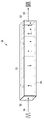
- FIG. 4 is a diagram showing a periodically poled waveguide having a structure in which the poling period of the core is changed in an inclined manner
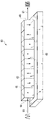
- FIG. 4 is a diagram showing a periodically poled waveguide having a structure in which the width of the core is changed in an inclined manner
- FIG. 10 is a diagram showing a wavelength conversion optical element having a structure with a changed poling period
- FIG. 10 is a diagram showing a wavelength conversion optical element in which the width of the core is changed in an inclined manner
- FIG. 10 is a diagram showing a wavelength conversion optical element having a structure with a changed poling period
- FIG. 4 is a diagram showing a wavelength conversion optical element in which the refractive index of the core is changed in a sloping manner
- a wavelength conversion optical element is a periodically poled waveguide that generates high-order harmonic light from an incident fundamental wave and emits desired wavelength-converted light from the output end of the element. be.
- the phase matching condition differs from the prior art in that the phase matching condition changes in an inclined manner from the entrance end to the exit end.
- the temperature of the element rises from the entrance end to the exit end. Therefore, in this embodiment, phase mismatching due to heat generation is suppressed by changing the function of the wavelength conversion optical element in an inclined manner so that phase matching can be achieved in a high-temperature environment as the phase matching condition approaches from the input end to the output end.
- FIG. 1 is a diagram showing a periodically poled waveguide having a structure in which the poling period of the core is changed in an inclined manner, according to one embodiment of the present invention. It is a diagram showing a core portion of a periodically poled waveguide, which may be either a ridge-type optical waveguide or an embedded waveguide.
- a periodically poled waveguide When the periodically poled waveguide is used as a ridge type optical waveguide or the like, at least part of the clad covering the periphery of the core becomes an air layer.
- the periodically poled waveguide 10 has a core 11 that converts the wavelength of light, an incident end 12 at which the fundamental light 14 is incident at one end on one side, and a converted wave 15 wavelength-converted by the core 11 at one end on the opposite side.
- the polarization inversion period becomes obliquely shorter as it approaches the output end 13 from the input end 12 . That is, in the optical axis direction of the periodically poled waveguide 10, the length of the region in which the polarization is set in one direction gradually shortens from the incident end 12 toward the exit end 13. .
- FIG. 2 is a diagram showing a periodically poled waveguide having a structure in which the width of the core is graded according to one embodiment of the present invention.
- the periodically poled waveguide 20 includes a core 21 that performs wavelength conversion of light, an incident end 22 that receives the fundamental light 24, and an output end 23 that outputs a converted wave 25 wavelength-converted by the core 21. It has a structure in which the width of the core 21 becomes obliquely shorter as it approaches the output end 23 from the end 22 . That is, in the optical axis direction of the periodically poled waveguide 20, the lengths of the regions in which the polarization is set in one direction are equal, and as the incident end 22 approaches the output end 23, the direction perpendicular to the optical axis direction is increased.
- the core 21 has a structure in which the width gradually decreases.
- a periodically poled waveguide is used in which the core structure changes in the optical axis direction so as not to break the phase matching condition shown in (Equation 4) as it approaches the output end from the incident end. This structure suppresses phase mismatch due to light absorption in the waveguide and accompanying heat generation, and can generate a converted wave with high efficiency.
- Materials that make up optical waveguides include silicon (Si), silicon dioxide (SiO 2 ), lithium niobate (LiNbO 3 ), lithium tantalate (LiTaO 3 ), indium phosphide (InP), dielectrics such as polymers, semiconductors, Alternatively, it is selected from nonlinear optical materials composed of compounds obtained by adding additives to these materials.
- FIG. 1 A first embodiment according to the present invention will now be described with reference to FIGS. 3 and 5.
- FIG. 1 As the core of the nonlinear optical waveguide approaches the output end, the polarization reversal period changes in a sloping manner.
- the present invention relates to a wavelength conversion element with a gradually changing wavelength.
- FIG. 3 is a diagram showing a wavelength conversion optical element having a structure in which the poling period is gradually changed according to one embodiment of the present invention.
- a wavelength conversion optical element 30 in this embodiment includes the periodically poled waveguide 10 shown in FIG. It has a structure in which the polarization inversion period becomes shorter as it approaches the output end 13 . That is, in the optical axis direction of the periodically poled waveguide 10, the length of the region in which the polarization is set in one direction gradually shortens from the incident end 12 toward the exit end 13. .
- the core 11 uses a LiNbO 3 -based ferroelectric and is directly bonded to the substrate 31 made of LiTaO 3 .
- Such a wavelength conversion optical element is designed to convert light in the 1.5 ⁇ m wavelength band into double wave light in the vicinity of a wavelength of 775 nm.
- the polarization reversal period in this embodiment is designed so that the phase is matched at the desired wavelength in the vicinity of the incident end 12, and the length of the region in which the polarization is set becomes shorter as the exit end 13 is approached. It is This corresponds to shifting the phase matching wavelength to the short wavelength side when using a nonlinear optical waveguide of LiNbO 3 system.
- the phase matching wavelength shifts to the longer wavelength side as the temperature rises. A converted wave can be generated efficiently.
- the wavelength conversion optical element in which the polarization inversion period of the core 11 is gradually changed from the entrance end 12 to the exit end 13 is not limited to the case where the core 11 is made of a LiNbO 3 -based ferroelectric material. . Therefore, it is also applicable to periodically poled waveguides using other nonlinear optical materials for the core 11. Similarly, by maintaining the phase matching condition, phase mismatch due to heat generation is suppressed, and the converted wave is efficiently generated. has the effect of generating
- the waveguide is an example of a ridge-type optical waveguide in which the core is directly bonded to the substrate, but as described above, the same effect can be obtained even with an embedded waveguide.
- a cladding 56 is provided surrounding the core 51 in the waveguide, as shown in FIG.
- FIG. 4 illustrates a wavelength conversion optical element with a graded core width, according to one embodiment of the present invention.
- the wavelength conversion optical element 40 in this embodiment includes the periodically poled waveguide 20 shown in FIG. It has a structure in which the width of the core 21 decreases obliquely as it approaches the output end 23 . That is, in the optical axis direction of the periodically poled waveguide 20, the lengths of the regions in which the polarization is set in one direction are equal, and as the incident end 22 approaches the output end 23, the direction perpendicular to the optical axis direction is increased.
- the core 21 has a structure in which the width gradually decreases.
- the core 21 of the wavelength conversion optical element here uses a LiNbO 3 -based ferroelectric material, and is directly bonded to a substrate 41 made of LiTaO 3 .
- Such a wavelength conversion optical element is designed to convert light in the 1.5 ⁇ m wavelength band into double wave light in the vicinity of a wavelength of 775 nm.
- the wavelength conversion optical element according to this embodiment configured as described above, quasi-phase matching in which polarization is periodically inverted is used for phase matching, as in the first embodiment. Also, this polarization inversion period is designed to be phase-matched at a desired wavelength in the vicinity of the incident end face. However, unlike the first embodiment, the polarization inversion period of the core 21 is constant. ing. This corresponds to shifting the phase matching wavelength to the short wavelength side when using a nonlinear optical waveguide of LiNbO 3 system. Therefore, by adopting such a form, it is possible to obtain the same effect as in the first embodiment and to generate a converted wave with high efficiency.
- the wavelength conversion optical element in which the width of the core 21 is changed from the entrance end 22 toward the exit end 23 is not limited to the case where the core 21 is made of a LiNbO 3 -based ferroelectric material. Therefore, even if the wavelength conversion optical element uses another nonlinear optical material for the core 21, the same effect can be obtained. Further, whether the width of the core 21 is shortened or lengthened from the entrance end 22 toward the exit end 23 depends on the nonlinear optical material and the structure of the element. Therefore, the change in width of core 21 is preferably designed to cancel the phase mismatch due to temperature rise of the device.
- the refractive index of the core changes in a gradient manner. It relates to a wavelength conversion optical element in which the refractive index in each region changes gradually with respect to the optical axis direction of the waveguide.
- FIG. 6 is a diagram showing a wavelength conversion optical element with a graded core refractive index according to one embodiment of the present invention.
- the wavelength conversion optical element 60 in this embodiment includes a periodically poled waveguide 61 and a substrate 63 bonded to the lower surface of a core 62 included in the periodically poled waveguide 61, and approaches an exit end 65 from an incident end 64. It has a structure in which the refractive index of the core 62 gradually decreases as it increases. That is, the core has a different refractive index for each period of the polarization inversion period, and the refractive index in each region gradually decreases as it approaches from the incident end 64 to the exit end 65 in the optical axis direction of the waveguide.
- the core 62 of the wavelength conversion optical element here uses a LiNbO 3 -based ferroelectric material, and is directly bonded to a substrate 63 made of LiTaO 3 .
- Such a wavelength conversion optical element is designed to convert light in the 1.5 ⁇ m wavelength band into double wave light in the vicinity of a wavelength of 775 nm.
- the polarization inversion period of the core 62 is constant, that is, the length of the region in which the polarization is set in one direction is equal in the optical axis direction of the periodically poled waveguide.
- the core width in the direction perpendicular to the optical axis direction of the core 62 is also constant.
- the refractive index of the core in the ridge type optical waveguide is gradually changed, but the refractive index of the clad in the embedded waveguide may be gradually changed.
- the refractive index may be gradually changed.
- the refractive index is changed by changing the composition ratio in this embodiment, the refractive index may be changed by applying other materials. In designing the structure of such an element, it is preferable to design so as to cancel the phase mismatch due to the temperature rise of the element.
- the present invention is expected to be used in the field of optical communication, the field of quantum information communication using light, and the field of optical measurement systems as a technology for generating a high-intensity converted wave with high efficiency.
Landscapes
- Physics & Mathematics (AREA)
- Nonlinear Science (AREA)
- General Physics & Mathematics (AREA)
- Optics & Photonics (AREA)
- Optical Integrated Circuits (AREA)
- Optical Modulation, Optical Deflection, Nonlinear Optics, Optical Demodulation, Optical Logic Elements (AREA)
Priority Applications (3)
| Application Number | Priority Date | Filing Date | Title |
|---|---|---|---|
| US18/548,815 US20240152025A1 (en) | 2021-04-12 | 2021-04-12 | Optical Wavelength Conversion Device |
| PCT/JP2021/015229 WO2022219687A1 (ja) | 2021-04-12 | 2021-04-12 | 波長変換光学素子 |
| JP2023514198A JPWO2022219687A1 (https=) | 2021-04-12 | 2021-04-12 |
Applications Claiming Priority (1)
| Application Number | Priority Date | Filing Date | Title |
|---|---|---|---|
| PCT/JP2021/015229 WO2022219687A1 (ja) | 2021-04-12 | 2021-04-12 | 波長変換光学素子 |
Publications (1)
| Publication Number | Publication Date |
|---|---|
| WO2022219687A1 true WO2022219687A1 (ja) | 2022-10-20 |
Family
ID=83639817
Family Applications (1)
| Application Number | Title | Priority Date | Filing Date |
|---|---|---|---|
| PCT/JP2021/015229 Ceased WO2022219687A1 (ja) | 2021-04-12 | 2021-04-12 | 波長変換光学素子 |
Country Status (3)
| Country | Link |
|---|---|
| US (1) | US20240152025A1 (https=) |
| JP (1) | JPWO2022219687A1 (https=) |
| WO (1) | WO2022219687A1 (https=) |
Families Citing this family (1)
| Publication number | Priority date | Publication date | Assignee | Title |
|---|---|---|---|---|
| US20240353733A1 (en) * | 2021-09-15 | 2024-10-24 | Nippon Telegraph And Telephone Corporation | Wavelength Conversion Device |
Citations (8)
| Publication number | Priority date | Publication date | Assignee | Title |
|---|---|---|---|---|
| JPH0643513A (ja) * | 1992-07-24 | 1994-02-18 | Ricoh Co Ltd | 波長変換素子 |
| WO2008050802A1 (en) * | 2006-10-27 | 2008-05-02 | Panasonic Corporation | Short wavelength light source and laser image forming device |
| WO2009047888A1 (ja) * | 2007-10-10 | 2009-04-16 | Panasonic Corporation | 固体レーザー装置及び画像表示装置 |
| US20090154508A1 (en) * | 2007-12-12 | 2009-06-18 | Hc Photonics Corp. | Light-generating apparatus with broadband pumping laser and quasi-phase matching waveguide |
| JP2017173827A (ja) * | 2016-03-21 | 2017-09-28 | ドイチェス エレクトローネン−シンクロトロン デズィDeutsches Elektronen−Synchrotron DESY | テラヘルツ放射を生成する方法および装置 |
| WO2018045701A1 (zh) * | 2016-09-07 | 2018-03-15 | 深圳大学 | 一种针对中红外脉冲激光的光谱调控装置 |
| JP2018073984A (ja) * | 2016-10-28 | 2018-05-10 | 大学共同利用機関法人自然科学研究機構 | レーザー部品 |
| JP2019073402A (ja) * | 2017-10-12 | 2019-05-16 | 国立大学法人三重大学 | 窒化物半導体基板、窒化物半導体基板の製造方法、窒化物半導体基板の製造装置及び窒化物半導体デバイス |
Family Cites Families (2)
| Publication number | Priority date | Publication date | Assignee | Title |
|---|---|---|---|---|
| JP5168867B2 (ja) * | 2006-09-29 | 2013-03-27 | 沖電気工業株式会社 | 波長変換素子 |
| US10141333B1 (en) * | 2017-11-09 | 2018-11-27 | International Business Machines Corporation | Domain wall control in ferroelectric devices |
-
2021
- 2021-04-12 US US18/548,815 patent/US20240152025A1/en not_active Abandoned
- 2021-04-12 WO PCT/JP2021/015229 patent/WO2022219687A1/ja not_active Ceased
- 2021-04-12 JP JP2023514198A patent/JPWO2022219687A1/ja active Pending
Patent Citations (8)
| Publication number | Priority date | Publication date | Assignee | Title |
|---|---|---|---|---|
| JPH0643513A (ja) * | 1992-07-24 | 1994-02-18 | Ricoh Co Ltd | 波長変換素子 |
| WO2008050802A1 (en) * | 2006-10-27 | 2008-05-02 | Panasonic Corporation | Short wavelength light source and laser image forming device |
| WO2009047888A1 (ja) * | 2007-10-10 | 2009-04-16 | Panasonic Corporation | 固体レーザー装置及び画像表示装置 |
| US20090154508A1 (en) * | 2007-12-12 | 2009-06-18 | Hc Photonics Corp. | Light-generating apparatus with broadband pumping laser and quasi-phase matching waveguide |
| JP2017173827A (ja) * | 2016-03-21 | 2017-09-28 | ドイチェス エレクトローネン−シンクロトロン デズィDeutsches Elektronen−Synchrotron DESY | テラヘルツ放射を生成する方法および装置 |
| WO2018045701A1 (zh) * | 2016-09-07 | 2018-03-15 | 深圳大学 | 一种针对中红外脉冲激光的光谱调控装置 |
| JP2018073984A (ja) * | 2016-10-28 | 2018-05-10 | 大学共同利用機関法人自然科学研究機構 | レーザー部品 |
| JP2019073402A (ja) * | 2017-10-12 | 2019-05-16 | 国立大学法人三重大学 | 窒化物半導体基板、窒化物半導体基板の製造方法、窒化物半導体基板の製造装置及び窒化物半導体デバイス |
Non-Patent Citations (1)
| Title |
|---|
| RYO TANABE, NAOKI YOKOYAMA, MASAHIRO UEMUKAI, TOMOYUKI TANIKAWA, RYUJI KATAYAMA: "Bonding Strength of Polarity-Inverted GaN Structure Fabricated by Surface-Activated Bonding", LECTURE PREPRINTS OF THE 80TH JSAP AUTUMN MEETING 2019, 18 September 2019 (2019-09-18) - 21 September 2019 (2019-09-21), pages 19a-E310-2, XP009540531 * |
Also Published As
| Publication number | Publication date |
|---|---|
| US20240152025A1 (en) | 2024-05-09 |
| JPWO2022219687A1 (https=) | 2022-10-20 |
Similar Documents
| Publication | Publication Date | Title |
|---|---|---|
| Wang et al. | Efficient second harmonic generation in a reverse‐polarization dual‐layer crystalline thin film nanophotonic waveguide | |
| CN112969960B (zh) | 波长转换装置 | |
| JP7160194B2 (ja) | 波長変換素子 | |
| US11815785B2 (en) | Wavelength conversion optical element | |
| JP2011039231A (ja) | 電磁波発振素子 | |
| JP7473850B2 (ja) | 波長変換装置 | |
| JP5814183B2 (ja) | 波長変換デバイス | |
| WO2022219687A1 (ja) | 波長変換光学素子 | |
| JP6774372B2 (ja) | 光学素子 | |
| Chen et al. | Analysis of cascaded second-order nonlinear interaction based on quasi-phase-matched optical waveguides | |
| JP7415195B2 (ja) | 波長変換素子 | |
| JP6348439B2 (ja) | 波長変換素子 | |
| JP7553868B2 (ja) | 波長変換装置及び波長変換装置の製造方法 | |
| JP7810905B2 (ja) | 波長変換器およびその制御方法 | |
| JP7617478B2 (ja) | 波長変換素子 | |
| WO2023218646A1 (ja) | 波長変換システム | |
| JPH0651359A (ja) | 波長変換素子、短波長レーザ装置および波長可変レーザ装置 | |
| JP2004109916A (ja) | 光通信用波長変換装置 | |
| JP4877258B2 (ja) | 波長変換素子 | |
| US20260086421A1 (en) | Manufacturing Method for Wavelength Conversion Elements | |
| JP3178849B2 (ja) | 導波路型shg素子 | |
| WO2023218667A1 (ja) | 波長変換装置 | |
| JP2007187920A (ja) | 非線形光学媒質およびそれを用いた波長変換装置 | |
| WO2026004145A1 (ja) | 光導波路 | |
| JP2015215501A (ja) | 波長変換素子 |
Legal Events
| Date | Code | Title | Description |
|---|---|---|---|
| 121 | Ep: the epo has been informed by wipo that ep was designated in this application |
Ref document number: 21936890 Country of ref document: EP Kind code of ref document: A1 |
|
| ENP | Entry into the national phase |
Ref document number: 2023514198 Country of ref document: JP Kind code of ref document: A |
|
| WWE | Wipo information: entry into national phase |
Ref document number: 18548815 Country of ref document: US |
|
| NENP | Non-entry into the national phase |
Ref country code: DE |
|
| 122 | Ep: pct application non-entry in european phase |
Ref document number: 21936890 Country of ref document: EP Kind code of ref document: A1 |