WO2022215621A1 - 積層体の製造方法、積層体の製造装置、積層体及び半導体装置 - Google Patents
積層体の製造方法、積層体の製造装置、積層体及び半導体装置 Download PDFInfo
- Publication number
- WO2022215621A1 WO2022215621A1 PCT/JP2022/015913 JP2022015913W WO2022215621A1 WO 2022215621 A1 WO2022215621 A1 WO 2022215621A1 JP 2022015913 W JP2022015913 W JP 2022015913W WO 2022215621 A1 WO2022215621 A1 WO 2022215621A1
- Authority
- WO
- WIPO (PCT)
- Prior art keywords
- substrate
- film
- stage
- laminate
- raw material
- Prior art date
- Legal status (The legal status is an assumption and is not a legal conclusion. Google has not performed a legal analysis and makes no representation as to the accuracy of the status listed.)
- Ceased
Links
Images


Classifications
-
- C—CHEMISTRY; METALLURGY
- C30—CRYSTAL GROWTH
- C30B—SINGLE-CRYSTAL GROWTH; UNIDIRECTIONAL SOLIDIFICATION OF EUTECTIC MATERIAL OR UNIDIRECTIONAL DEMIXING OF EUTECTOID MATERIAL; REFINING BY ZONE-MELTING OF MATERIAL; PRODUCTION OF A HOMOGENEOUS POLYCRYSTALLINE MATERIAL WITH DEFINED STRUCTURE; SINGLE CRYSTALS OR HOMOGENEOUS POLYCRYSTALLINE MATERIAL WITH DEFINED STRUCTURE; AFTER-TREATMENT OF SINGLE CRYSTALS OR A HOMOGENEOUS POLYCRYSTALLINE MATERIAL WITH DEFINED STRUCTURE; APPARATUS THEREFOR
- C30B29/00—Single crystals or homogeneous polycrystalline material with defined structure characterised by the material or by their shape
- C30B29/10—Inorganic compounds or compositions
- C30B29/16—Oxides
-
- C—CHEMISTRY; METALLURGY
- C23—COATING METALLIC MATERIAL; COATING MATERIAL WITH METALLIC MATERIAL; CHEMICAL SURFACE TREATMENT; DIFFUSION TREATMENT OF METALLIC MATERIAL; COATING BY VACUUM EVAPORATION, BY SPUTTERING, BY ION IMPLANTATION OR BY CHEMICAL VAPOUR DEPOSITION, IN GENERAL; INHIBITING CORROSION OF METALLIC MATERIAL OR INCRUSTATION IN GENERAL
- C23C—COATING METALLIC MATERIAL; COATING MATERIAL WITH METALLIC MATERIAL; SURFACE TREATMENT OF METALLIC MATERIAL BY DIFFUSION INTO THE SURFACE, BY CHEMICAL CONVERSION OR SUBSTITUTION; COATING BY VACUUM EVAPORATION, BY SPUTTERING, BY ION IMPLANTATION OR BY CHEMICAL VAPOUR DEPOSITION, IN GENERAL
- C23C16/00—Chemical coating by decomposition of gaseous compounds, without leaving reaction products of surface material in the coating, i.e. chemical vapour deposition [CVD] processes
- C23C16/02—Pretreatment of the material to be coated
- C23C16/0272—Deposition of sub-layers, e.g. to promote the adhesion of the main coating
-
- C—CHEMISTRY; METALLURGY
- C23—COATING METALLIC MATERIAL; COATING MATERIAL WITH METALLIC MATERIAL; CHEMICAL SURFACE TREATMENT; DIFFUSION TREATMENT OF METALLIC MATERIAL; COATING BY VACUUM EVAPORATION, BY SPUTTERING, BY ION IMPLANTATION OR BY CHEMICAL VAPOUR DEPOSITION, IN GENERAL; INHIBITING CORROSION OF METALLIC MATERIAL OR INCRUSTATION IN GENERAL
- C23C—COATING METALLIC MATERIAL; COATING MATERIAL WITH METALLIC MATERIAL; SURFACE TREATMENT OF METALLIC MATERIAL BY DIFFUSION INTO THE SURFACE, BY CHEMICAL CONVERSION OR SUBSTITUTION; COATING BY VACUUM EVAPORATION, BY SPUTTERING, BY ION IMPLANTATION OR BY CHEMICAL VAPOUR DEPOSITION, IN GENERAL
- C23C16/00—Chemical coating by decomposition of gaseous compounds, without leaving reaction products of surface material in the coating, i.e. chemical vapour deposition [CVD] processes
- C23C16/22—Chemical coating by decomposition of gaseous compounds, without leaving reaction products of surface material in the coating, i.e. chemical vapour deposition [CVD] processes characterised by the deposition of inorganic material, other than metallic material
- C23C16/30—Deposition of compounds, mixtures or solid solutions, e.g. borides, carbides, nitrides
- C23C16/40—Oxides
-
- C—CHEMISTRY; METALLURGY
- C23—COATING METALLIC MATERIAL; COATING MATERIAL WITH METALLIC MATERIAL; CHEMICAL SURFACE TREATMENT; DIFFUSION TREATMENT OF METALLIC MATERIAL; COATING BY VACUUM EVAPORATION, BY SPUTTERING, BY ION IMPLANTATION OR BY CHEMICAL VAPOUR DEPOSITION, IN GENERAL; INHIBITING CORROSION OF METALLIC MATERIAL OR INCRUSTATION IN GENERAL
- C23C—COATING METALLIC MATERIAL; COATING MATERIAL WITH METALLIC MATERIAL; SURFACE TREATMENT OF METALLIC MATERIAL BY DIFFUSION INTO THE SURFACE, BY CHEMICAL CONVERSION OR SUBSTITUTION; COATING BY VACUUM EVAPORATION, BY SPUTTERING, BY ION IMPLANTATION OR BY CHEMICAL VAPOUR DEPOSITION, IN GENERAL
- C23C16/00—Chemical coating by decomposition of gaseous compounds, without leaving reaction products of surface material in the coating, i.e. chemical vapour deposition [CVD] processes
- C23C16/44—Chemical coating by decomposition of gaseous compounds, without leaving reaction products of surface material in the coating, i.e. chemical vapour deposition [CVD] processes characterised by the method of coating
- C23C16/448—Chemical coating by decomposition of gaseous compounds, without leaving reaction products of surface material in the coating, i.e. chemical vapour deposition [CVD] processes characterised by the method of coating characterised by the method used for generating reactive gas streams, e.g. by evaporation or sublimation of precursor materials
- C23C16/4481—Chemical coating by decomposition of gaseous compounds, without leaving reaction products of surface material in the coating, i.e. chemical vapour deposition [CVD] processes characterised by the method of coating characterised by the method used for generating reactive gas streams, e.g. by evaporation or sublimation of precursor materials by evaporation using carrier gas in contact with the source material
-
- C—CHEMISTRY; METALLURGY
- C23—COATING METALLIC MATERIAL; COATING MATERIAL WITH METALLIC MATERIAL; CHEMICAL SURFACE TREATMENT; DIFFUSION TREATMENT OF METALLIC MATERIAL; COATING BY VACUUM EVAPORATION, BY SPUTTERING, BY ION IMPLANTATION OR BY CHEMICAL VAPOUR DEPOSITION, IN GENERAL; INHIBITING CORROSION OF METALLIC MATERIAL OR INCRUSTATION IN GENERAL
- C23C—COATING METALLIC MATERIAL; COATING MATERIAL WITH METALLIC MATERIAL; SURFACE TREATMENT OF METALLIC MATERIAL BY DIFFUSION INTO THE SURFACE, BY CHEMICAL CONVERSION OR SUBSTITUTION; COATING BY VACUUM EVAPORATION, BY SPUTTERING, BY ION IMPLANTATION OR BY CHEMICAL VAPOUR DEPOSITION, IN GENERAL
- C23C16/00—Chemical coating by decomposition of gaseous compounds, without leaving reaction products of surface material in the coating, i.e. chemical vapour deposition [CVD] processes
- C23C16/44—Chemical coating by decomposition of gaseous compounds, without leaving reaction products of surface material in the coating, i.e. chemical vapour deposition [CVD] processes characterised by the method of coating
- C23C16/448—Chemical coating by decomposition of gaseous compounds, without leaving reaction products of surface material in the coating, i.e. chemical vapour deposition [CVD] processes characterised by the method of coating characterised by the method used for generating reactive gas streams, e.g. by evaporation or sublimation of precursor materials
- C23C16/4486—Chemical coating by decomposition of gaseous compounds, without leaving reaction products of surface material in the coating, i.e. chemical vapour deposition [CVD] processes characterised by the method of coating characterised by the method used for generating reactive gas streams, e.g. by evaporation or sublimation of precursor materials by producing an aerosol and subsequent evaporation of the droplets or particles
-
- C—CHEMISTRY; METALLURGY
- C23—COATING METALLIC MATERIAL; COATING MATERIAL WITH METALLIC MATERIAL; CHEMICAL SURFACE TREATMENT; DIFFUSION TREATMENT OF METALLIC MATERIAL; COATING BY VACUUM EVAPORATION, BY SPUTTERING, BY ION IMPLANTATION OR BY CHEMICAL VAPOUR DEPOSITION, IN GENERAL; INHIBITING CORROSION OF METALLIC MATERIAL OR INCRUSTATION IN GENERAL
- C23C—COATING METALLIC MATERIAL; COATING MATERIAL WITH METALLIC MATERIAL; SURFACE TREATMENT OF METALLIC MATERIAL BY DIFFUSION INTO THE SURFACE, BY CHEMICAL CONVERSION OR SUBSTITUTION; COATING BY VACUUM EVAPORATION, BY SPUTTERING, BY ION IMPLANTATION OR BY CHEMICAL VAPOUR DEPOSITION, IN GENERAL
- C23C16/00—Chemical coating by decomposition of gaseous compounds, without leaving reaction products of surface material in the coating, i.e. chemical vapour deposition [CVD] processes
- C23C16/44—Chemical coating by decomposition of gaseous compounds, without leaving reaction products of surface material in the coating, i.e. chemical vapour deposition [CVD] processes characterised by the method of coating
- C23C16/455—Chemical coating by decomposition of gaseous compounds, without leaving reaction products of surface material in the coating, i.e. chemical vapour deposition [CVD] processes characterised by the method of coating characterised by the method used for introducing gases into reaction chamber or for modifying gas flows in reaction chamber
- C23C16/45512—Premixing before introduction in the reaction chamber
-
- C—CHEMISTRY; METALLURGY
- C23—COATING METALLIC MATERIAL; COATING MATERIAL WITH METALLIC MATERIAL; CHEMICAL SURFACE TREATMENT; DIFFUSION TREATMENT OF METALLIC MATERIAL; COATING BY VACUUM EVAPORATION, BY SPUTTERING, BY ION IMPLANTATION OR BY CHEMICAL VAPOUR DEPOSITION, IN GENERAL; INHIBITING CORROSION OF METALLIC MATERIAL OR INCRUSTATION IN GENERAL
- C23C—COATING METALLIC MATERIAL; COATING MATERIAL WITH METALLIC MATERIAL; SURFACE TREATMENT OF METALLIC MATERIAL BY DIFFUSION INTO THE SURFACE, BY CHEMICAL CONVERSION OR SUBSTITUTION; COATING BY VACUUM EVAPORATION, BY SPUTTERING, BY ION IMPLANTATION OR BY CHEMICAL VAPOUR DEPOSITION, IN GENERAL
- C23C16/00—Chemical coating by decomposition of gaseous compounds, without leaving reaction products of surface material in the coating, i.e. chemical vapour deposition [CVD] processes
- C23C16/44—Chemical coating by decomposition of gaseous compounds, without leaving reaction products of surface material in the coating, i.e. chemical vapour deposition [CVD] processes characterised by the method of coating
- C23C16/458—Chemical coating by decomposition of gaseous compounds, without leaving reaction products of surface material in the coating, i.e. chemical vapour deposition [CVD] processes characterised by the method of coating characterised by the method used for supporting substrates in the reaction chamber
- C23C16/4581—Chemical coating by decomposition of gaseous compounds, without leaving reaction products of surface material in the coating, i.e. chemical vapour deposition [CVD] processes characterised by the method of coating characterised by the method used for supporting substrates in the reaction chamber characterised by material of construction or surface finish of the means for supporting the substrate
-
- C—CHEMISTRY; METALLURGY
- C23—COATING METALLIC MATERIAL; COATING MATERIAL WITH METALLIC MATERIAL; CHEMICAL SURFACE TREATMENT; DIFFUSION TREATMENT OF METALLIC MATERIAL; COATING BY VACUUM EVAPORATION, BY SPUTTERING, BY ION IMPLANTATION OR BY CHEMICAL VAPOUR DEPOSITION, IN GENERAL; INHIBITING CORROSION OF METALLIC MATERIAL OR INCRUSTATION IN GENERAL
- C23C—COATING METALLIC MATERIAL; COATING MATERIAL WITH METALLIC MATERIAL; SURFACE TREATMENT OF METALLIC MATERIAL BY DIFFUSION INTO THE SURFACE, BY CHEMICAL CONVERSION OR SUBSTITUTION; COATING BY VACUUM EVAPORATION, BY SPUTTERING, BY ION IMPLANTATION OR BY CHEMICAL VAPOUR DEPOSITION, IN GENERAL
- C23C16/00—Chemical coating by decomposition of gaseous compounds, without leaving reaction products of surface material in the coating, i.e. chemical vapour deposition [CVD] processes
- C23C16/44—Chemical coating by decomposition of gaseous compounds, without leaving reaction products of surface material in the coating, i.e. chemical vapour deposition [CVD] processes characterised by the method of coating
- C23C16/458—Chemical coating by decomposition of gaseous compounds, without leaving reaction products of surface material in the coating, i.e. chemical vapour deposition [CVD] processes characterised by the method of coating characterised by the method used for supporting substrates in the reaction chamber
- C23C16/4582—Rigid and flat substrates, e.g. plates or discs
- C23C16/4583—Rigid and flat substrates, e.g. plates or discs the substrate being supported substantially horizontally
-
- C—CHEMISTRY; METALLURGY
- C23—COATING METALLIC MATERIAL; COATING MATERIAL WITH METALLIC MATERIAL; CHEMICAL SURFACE TREATMENT; DIFFUSION TREATMENT OF METALLIC MATERIAL; COATING BY VACUUM EVAPORATION, BY SPUTTERING, BY ION IMPLANTATION OR BY CHEMICAL VAPOUR DEPOSITION, IN GENERAL; INHIBITING CORROSION OF METALLIC MATERIAL OR INCRUSTATION IN GENERAL
- C23C—COATING METALLIC MATERIAL; COATING MATERIAL WITH METALLIC MATERIAL; SURFACE TREATMENT OF METALLIC MATERIAL BY DIFFUSION INTO THE SURFACE, BY CHEMICAL CONVERSION OR SUBSTITUTION; COATING BY VACUUM EVAPORATION, BY SPUTTERING, BY ION IMPLANTATION OR BY CHEMICAL VAPOUR DEPOSITION, IN GENERAL
- C23C16/00—Chemical coating by decomposition of gaseous compounds, without leaving reaction products of surface material in the coating, i.e. chemical vapour deposition [CVD] processes
- C23C16/44—Chemical coating by decomposition of gaseous compounds, without leaving reaction products of surface material in the coating, i.e. chemical vapour deposition [CVD] processes characterised by the method of coating
- C23C16/458—Chemical coating by decomposition of gaseous compounds, without leaving reaction products of surface material in the coating, i.e. chemical vapour deposition [CVD] processes characterised by the method of coating characterised by the method used for supporting substrates in the reaction chamber
- C23C16/4582—Rigid and flat substrates, e.g. plates or discs
- C23C16/4583—Rigid and flat substrates, e.g. plates or discs the substrate being supported substantially horizontally
- C23C16/4586—Elements in the interior of the support, e.g. electrodes, heating or cooling devices
-
- C—CHEMISTRY; METALLURGY
- C23—COATING METALLIC MATERIAL; COATING MATERIAL WITH METALLIC MATERIAL; CHEMICAL SURFACE TREATMENT; DIFFUSION TREATMENT OF METALLIC MATERIAL; COATING BY VACUUM EVAPORATION, BY SPUTTERING, BY ION IMPLANTATION OR BY CHEMICAL VAPOUR DEPOSITION, IN GENERAL; INHIBITING CORROSION OF METALLIC MATERIAL OR INCRUSTATION IN GENERAL
- C23C—COATING METALLIC MATERIAL; COATING MATERIAL WITH METALLIC MATERIAL; SURFACE TREATMENT OF METALLIC MATERIAL BY DIFFUSION INTO THE SURFACE, BY CHEMICAL CONVERSION OR SUBSTITUTION; COATING BY VACUUM EVAPORATION, BY SPUTTERING, BY ION IMPLANTATION OR BY CHEMICAL VAPOUR DEPOSITION, IN GENERAL
- C23C16/00—Chemical coating by decomposition of gaseous compounds, without leaving reaction products of surface material in the coating, i.e. chemical vapour deposition [CVD] processes
- C23C16/44—Chemical coating by decomposition of gaseous compounds, without leaving reaction products of surface material in the coating, i.e. chemical vapour deposition [CVD] processes characterised by the method of coating
- C23C16/46—Chemical coating by decomposition of gaseous compounds, without leaving reaction products of surface material in the coating, i.e. chemical vapour deposition [CVD] processes characterised by the method of coating characterised by the method used for heating the substrate
-
- C—CHEMISTRY; METALLURGY
- C30—CRYSTAL GROWTH
- C30B—SINGLE-CRYSTAL GROWTH; UNIDIRECTIONAL SOLIDIFICATION OF EUTECTIC MATERIAL OR UNIDIRECTIONAL DEMIXING OF EUTECTOID MATERIAL; REFINING BY ZONE-MELTING OF MATERIAL; PRODUCTION OF A HOMOGENEOUS POLYCRYSTALLINE MATERIAL WITH DEFINED STRUCTURE; SINGLE CRYSTALS OR HOMOGENEOUS POLYCRYSTALLINE MATERIAL WITH DEFINED STRUCTURE; AFTER-TREATMENT OF SINGLE CRYSTALS OR A HOMOGENEOUS POLYCRYSTALLINE MATERIAL WITH DEFINED STRUCTURE; APPARATUS THEREFOR
- C30B25/00—Single-crystal growth by chemical reaction of reactive gases, e.g. chemical vapour-deposition growth
- C30B25/02—Epitaxial-layer growth
- C30B25/10—Heating of the reaction chamber or the substrate
-
- C—CHEMISTRY; METALLURGY
- C30—CRYSTAL GROWTH
- C30B—SINGLE-CRYSTAL GROWTH; UNIDIRECTIONAL SOLIDIFICATION OF EUTECTIC MATERIAL OR UNIDIRECTIONAL DEMIXING OF EUTECTOID MATERIAL; REFINING BY ZONE-MELTING OF MATERIAL; PRODUCTION OF A HOMOGENEOUS POLYCRYSTALLINE MATERIAL WITH DEFINED STRUCTURE; SINGLE CRYSTALS OR HOMOGENEOUS POLYCRYSTALLINE MATERIAL WITH DEFINED STRUCTURE; AFTER-TREATMENT OF SINGLE CRYSTALS OR A HOMOGENEOUS POLYCRYSTALLINE MATERIAL WITH DEFINED STRUCTURE; APPARATUS THEREFOR
- C30B25/00—Single-crystal growth by chemical reaction of reactive gases, e.g. chemical vapour-deposition growth
- C30B25/02—Epitaxial-layer growth
- C30B25/14—Feed and outlet means for the gases; Modifying the flow of the reactive gases
-
- C—CHEMISTRY; METALLURGY
- C30—CRYSTAL GROWTH
- C30B—SINGLE-CRYSTAL GROWTH; UNIDIRECTIONAL SOLIDIFICATION OF EUTECTIC MATERIAL OR UNIDIRECTIONAL DEMIXING OF EUTECTOID MATERIAL; REFINING BY ZONE-MELTING OF MATERIAL; PRODUCTION OF A HOMOGENEOUS POLYCRYSTALLINE MATERIAL WITH DEFINED STRUCTURE; SINGLE CRYSTALS OR HOMOGENEOUS POLYCRYSTALLINE MATERIAL WITH DEFINED STRUCTURE; AFTER-TREATMENT OF SINGLE CRYSTALS OR A HOMOGENEOUS POLYCRYSTALLINE MATERIAL WITH DEFINED STRUCTURE; APPARATUS THEREFOR
- C30B25/00—Single-crystal growth by chemical reaction of reactive gases, e.g. chemical vapour-deposition growth
- C30B25/02—Epitaxial-layer growth
- C30B25/16—Controlling or regulating
- C30B25/165—Controlling or regulating the flow of the reactive gases
-
- C—CHEMISTRY; METALLURGY
- C30—CRYSTAL GROWTH
- C30B—SINGLE-CRYSTAL GROWTH; UNIDIRECTIONAL SOLIDIFICATION OF EUTECTIC MATERIAL OR UNIDIRECTIONAL DEMIXING OF EUTECTOID MATERIAL; REFINING BY ZONE-MELTING OF MATERIAL; PRODUCTION OF A HOMOGENEOUS POLYCRYSTALLINE MATERIAL WITH DEFINED STRUCTURE; SINGLE CRYSTALS OR HOMOGENEOUS POLYCRYSTALLINE MATERIAL WITH DEFINED STRUCTURE; AFTER-TREATMENT OF SINGLE CRYSTALS OR A HOMOGENEOUS POLYCRYSTALLINE MATERIAL WITH DEFINED STRUCTURE; APPARATUS THEREFOR
- C30B25/00—Single-crystal growth by chemical reaction of reactive gases, e.g. chemical vapour-deposition growth
- C30B25/02—Epitaxial-layer growth
- C30B25/18—Epitaxial-layer growth characterised by the substrate
-
- H—ELECTRICITY
- H10—SEMICONDUCTOR DEVICES; ELECTRIC SOLID-STATE DEVICES NOT OTHERWISE PROVIDED FOR
- H10P—GENERIC PROCESSES OR APPARATUS FOR THE MANUFACTURE OR TREATMENT OF DEVICES COVERED BY CLASS H10
- H10P14/00—Formation of materials, e.g. in the shape of layers or pillars
- H10P14/20—Formation of materials, e.g. in the shape of layers or pillars of semiconductor materials
- H10P14/24—Formation of materials, e.g. in the shape of layers or pillars of semiconductor materials using chemical vapour deposition [CVD]
-
- H—ELECTRICITY
- H10—SEMICONDUCTOR DEVICES; ELECTRIC SOLID-STATE DEVICES NOT OTHERWISE PROVIDED FOR
- H10P—GENERIC PROCESSES OR APPARATUS FOR THE MANUFACTURE OR TREATMENT OF DEVICES COVERED BY CLASS H10
- H10P14/00—Formation of materials, e.g. in the shape of layers or pillars
- H10P14/20—Formation of materials, e.g. in the shape of layers or pillars of semiconductor materials
- H10P14/26—Formation of materials, e.g. in the shape of layers or pillars of semiconductor materials using liquid deposition
- H10P14/265—Formation of materials, e.g. in the shape of layers or pillars of semiconductor materials using liquid deposition using solutions
-
- H—ELECTRICITY
- H10—SEMICONDUCTOR DEVICES; ELECTRIC SOLID-STATE DEVICES NOT OTHERWISE PROVIDED FOR
- H10P—GENERIC PROCESSES OR APPARATUS FOR THE MANUFACTURE OR TREATMENT OF DEVICES COVERED BY CLASS H10
- H10P14/00—Formation of materials, e.g. in the shape of layers or pillars
- H10P14/20—Formation of materials, e.g. in the shape of layers or pillars of semiconductor materials
- H10P14/29—Formation of materials, e.g. in the shape of layers or pillars of semiconductor materials characterised by the substrates
- H10P14/2901—Materials
- H10P14/2921—Materials being crystalline insulating materials
-
- H—ELECTRICITY
- H10—SEMICONDUCTOR DEVICES; ELECTRIC SOLID-STATE DEVICES NOT OTHERWISE PROVIDED FOR
- H10P—GENERIC PROCESSES OR APPARATUS FOR THE MANUFACTURE OR TREATMENT OF DEVICES COVERED BY CLASS H10
- H10P14/00—Formation of materials, e.g. in the shape of layers or pillars
- H10P14/20—Formation of materials, e.g. in the shape of layers or pillars of semiconductor materials
- H10P14/29—Formation of materials, e.g. in the shape of layers or pillars of semiconductor materials characterised by the substrates
- H10P14/2924—Structures
-
- H—ELECTRICITY
- H10—SEMICONDUCTOR DEVICES; ELECTRIC SOLID-STATE DEVICES NOT OTHERWISE PROVIDED FOR
- H10P—GENERIC PROCESSES OR APPARATUS FOR THE MANUFACTURE OR TREATMENT OF DEVICES COVERED BY CLASS H10
- H10P14/00—Formation of materials, e.g. in the shape of layers or pillars
- H10P14/20—Formation of materials, e.g. in the shape of layers or pillars of semiconductor materials
- H10P14/29—Formation of materials, e.g. in the shape of layers or pillars of semiconductor materials characterised by the substrates
- H10P14/2924—Structures
- H10P14/2925—Surface structures
-
- H—ELECTRICITY
- H10—SEMICONDUCTOR DEVICES; ELECTRIC SOLID-STATE DEVICES NOT OTHERWISE PROVIDED FOR
- H10P—GENERIC PROCESSES OR APPARATUS FOR THE MANUFACTURE OR TREATMENT OF DEVICES COVERED BY CLASS H10
- H10P14/00—Formation of materials, e.g. in the shape of layers or pillars
- H10P14/20—Formation of materials, e.g. in the shape of layers or pillars of semiconductor materials
- H10P14/32—Formation of materials, e.g. in the shape of layers or pillars of semiconductor materials characterised by intermediate layers between substrates and deposited layers
- H10P14/3202—Materials thereof
-
- H—ELECTRICITY
- H10—SEMICONDUCTOR DEVICES; ELECTRIC SOLID-STATE DEVICES NOT OTHERWISE PROVIDED FOR
- H10P—GENERIC PROCESSES OR APPARATUS FOR THE MANUFACTURE OR TREATMENT OF DEVICES COVERED BY CLASS H10
- H10P14/00—Formation of materials, e.g. in the shape of layers or pillars
- H10P14/20—Formation of materials, e.g. in the shape of layers or pillars of semiconductor materials
- H10P14/32—Formation of materials, e.g. in the shape of layers or pillars of semiconductor materials characterised by intermediate layers between substrates and deposited layers
- H10P14/3202—Materials thereof
- H10P14/3234—Materials thereof being oxide semiconducting materials
-
- H—ELECTRICITY
- H10—SEMICONDUCTOR DEVICES; ELECTRIC SOLID-STATE DEVICES NOT OTHERWISE PROVIDED FOR
- H10P—GENERIC PROCESSES OR APPARATUS FOR THE MANUFACTURE OR TREATMENT OF DEVICES COVERED BY CLASS H10
- H10P14/00—Formation of materials, e.g. in the shape of layers or pillars
- H10P14/20—Formation of materials, e.g. in the shape of layers or pillars of semiconductor materials
- H10P14/32—Formation of materials, e.g. in the shape of layers or pillars of semiconductor materials characterised by intermediate layers between substrates and deposited layers
- H10P14/3202—Materials thereof
- H10P14/3238—Materials thereof being insulating materials
-
- H—ELECTRICITY
- H10—SEMICONDUCTOR DEVICES; ELECTRIC SOLID-STATE DEVICES NOT OTHERWISE PROVIDED FOR
- H10P—GENERIC PROCESSES OR APPARATUS FOR THE MANUFACTURE OR TREATMENT OF DEVICES COVERED BY CLASS H10
- H10P14/00—Formation of materials, e.g. in the shape of layers or pillars
- H10P14/20—Formation of materials, e.g. in the shape of layers or pillars of semiconductor materials
- H10P14/34—Deposited materials, e.g. layers
- H10P14/3402—Deposited materials, e.g. layers characterised by the chemical composition
- H10P14/3434—Deposited materials, e.g. layers characterised by the chemical composition being oxide semiconductor materials
-
- H—ELECTRICITY
- H10—SEMICONDUCTOR DEVICES; ELECTRIC SOLID-STATE DEVICES NOT OTHERWISE PROVIDED FOR
- H10P—GENERIC PROCESSES OR APPARATUS FOR THE MANUFACTURE OR TREATMENT OF DEVICES COVERED BY CLASS H10
- H10P14/00—Formation of materials, e.g. in the shape of layers or pillars
- H10P14/20—Formation of materials, e.g. in the shape of layers or pillars of semiconductor materials
- H10P14/34—Deposited materials, e.g. layers
- H10P14/3438—Doping during depositing
- H10P14/3441—Conductivity type
- H10P14/3442—N-type
-
- H—ELECTRICITY
- H10—SEMICONDUCTOR DEVICES; ELECTRIC SOLID-STATE DEVICES NOT OTHERWISE PROVIDED FOR
- H10P—GENERIC PROCESSES OR APPARATUS FOR THE MANUFACTURE OR TREATMENT OF DEVICES COVERED BY CLASS H10
- H10P14/00—Formation of materials, e.g. in the shape of layers or pillars
- H10P14/20—Formation of materials, e.g. in the shape of layers or pillars of semiconductor materials
- H10P14/34—Deposited materials, e.g. layers
- H10P14/3438—Doping during depositing
- H10P14/3441—Conductivity type
- H10P14/3444—P-type
-
- H—ELECTRICITY
- H10—SEMICONDUCTOR DEVICES; ELECTRIC SOLID-STATE DEVICES NOT OTHERWISE PROVIDED FOR
- H10P—GENERIC PROCESSES OR APPARATUS FOR THE MANUFACTURE OR TREATMENT OF DEVICES COVERED BY CLASS H10
- H10P14/00—Formation of materials, e.g. in the shape of layers or pillars
- H10P14/20—Formation of materials, e.g. in the shape of layers or pillars of semiconductor materials
- H10P14/34—Deposited materials, e.g. layers
- H10P14/3438—Doping during depositing
- H10P14/3441—Conductivity type
- H10P14/3446—Transition metal elements; Rare earth elements
-
- H—ELECTRICITY
- H10—SEMICONDUCTOR DEVICES; ELECTRIC SOLID-STATE DEVICES NOT OTHERWISE PROVIDED FOR
- H10P—GENERIC PROCESSES OR APPARATUS FOR THE MANUFACTURE OR TREATMENT OF DEVICES COVERED BY CLASS H10
- H10P14/00—Formation of materials, e.g. in the shape of layers or pillars
- H10P14/20—Formation of materials, e.g. in the shape of layers or pillars of semiconductor materials
- H10P14/34—Deposited materials, e.g. layers
- H10P14/3451—Structure
-
- H—ELECTRICITY
- H10—SEMICONDUCTOR DEVICES; ELECTRIC SOLID-STATE DEVICES NOT OTHERWISE PROVIDED FOR
- H10P—GENERIC PROCESSES OR APPARATUS FOR THE MANUFACTURE OR TREATMENT OF DEVICES COVERED BY CLASS H10
- H10P14/00—Formation of materials, e.g. in the shape of layers or pillars
- H10P14/60—Formation of materials, e.g. in the shape of layers or pillars of insulating materials
- H10P14/63—Formation of materials, e.g. in the shape of layers or pillars of insulating materials characterised by the formation processes
- H10P14/6326—Deposition processes
- H10P14/6328—Deposition from the gas or vapour phase
- H10P14/6334—Deposition from the gas or vapour phase using decomposition or reaction of gaseous or vapour phase compounds, i.e. chemical vapour deposition
-
- H—ELECTRICITY
- H10—SEMICONDUCTOR DEVICES; ELECTRIC SOLID-STATE DEVICES NOT OTHERWISE PROVIDED FOR
- H10P—GENERIC PROCESSES OR APPARATUS FOR THE MANUFACTURE OR TREATMENT OF DEVICES COVERED BY CLASS H10
- H10P14/00—Formation of materials, e.g. in the shape of layers or pillars
- H10P14/60—Formation of materials, e.g. in the shape of layers or pillars of insulating materials
- H10P14/69—Inorganic materials
- H10P14/692—Inorganic materials composed of oxides, glassy oxides or oxide-based glasses
- H10P14/6938—Inorganic materials composed of oxides, glassy oxides or oxide-based glasses the material containing at least one metal element, e.g. metal oxides, metal oxynitrides or metal oxycarbides
- H10P14/6939—Inorganic materials composed of oxides, glassy oxides or oxide-based glasses the material containing at least one metal element, e.g. metal oxides, metal oxynitrides or metal oxycarbides characterised by the metal
Definitions
- the present invention relates to a laminate manufacturing method, a laminate manufacturing apparatus, a laminate, and a semiconductor device.
- Mist Chemical Vapor Deposition is known as a method capable of forming a highly crystalline corundum-type crystal thin film on a substrate.
- a solution using a gallium acetylacetonate complex is misted and supplied to a sapphire substrate on a substrate installed in a narrow space (fine channel) provided in a reactor, and ⁇ - A method of forming a Ga2O3 film is described.
- a sapphire substrate is placed on a hot plate installed in a film formation chamber, and a raw material solution mist made from gallium bromide is supplied to the substrate from a nozzle installed above the substrate.
- a method of forming an ⁇ -Ga 2 O 3 film is described.
- a corundum-type crystal thin film when used as a semiconductor device, it generally requires a thickness of several hundred nm or more, and when used as a power device, a thickness of 1 ⁇ m or more is required.
- the gallium oxide-based thin film formed by the mist CVD method has a problem that the crystal quality is remarkably deteriorated as the film thickness increases. Moreover, there is a problem that this problem becomes more conspicuous especially in a film thickness of 1 ⁇ m or more.
- the present invention has been made to solve the above problems, a thick film of a high-quality corundum-type crystal thin film (semiconductor film having a corundum-type crystal structure) with excellent crystal orientation can be stably formed lamination
- the object is to provide a method for manufacturing a body.
- Another object of the present invention is to provide a high-quality laminate suitable for manufacturing a semiconductor device.
- a method for manufacturing a laminate comprising a semiconductor film having a corundum-type crystal structure, placing the substrate on a stage; heating the substrate; atomizing the film-forming raw material solution; mixing the atomized film-forming raw material solution and a carrier gas to form a mixture; and forming a film by supplying the gas mixture to the substrate,
- a method for manufacturing a laminate wherein the surface roughness Ra of the contact surface of the stage with the substrate and the surface roughness Ra of the contact surface of the substrate with the stage is 0.5 ⁇ m or less.
- a laminate containing a semiconductor film having a high-quality corundum-type crystal structure can be manufactured more stably and inexpensively.
- the waviness Wa of the contact surface of the stage with the base and the contact surface of the base with the stage be 50 ⁇ m or less.
- the temperature of the substrate can be easily maintained, so that a high-quality laminate can be stably produced.
- a substrate having a thickness of 50 ⁇ m or more and 5000 ⁇ m or less it is preferable to use a substrate having a thickness of 50 ⁇ m or more and 5000 ⁇ m or less.
- the step of placing the substrate on the stage further includes the step of vacuum fixing the substrate to the stage, and the degree of vacuum is 80 kPa or less.
- the substrate can be held and heated stably, so that a laminate of even higher quality can be obtained.
- the present invention provides an apparatus for manufacturing a laminate including a semiconductor film having a corundum type crystal structure, a stage on which the substrate is placed; heating means for heating the substrate; atomizing means for atomizing the film-forming raw material solution; a mixture supplying means for mixing the atomized film-forming raw material solution and a carrier gas and supplying the mixture to the substrate;
- an apparatus for manufacturing a laminate wherein the surface roughness Ra of the contact surface with the substrate on the stage is 0.5 ⁇ m or less.
- the waviness Wa of the contact surface of the stage with the substrate is 50 ⁇ m or less.
- the present invention is a laminate, A substrate and a semiconductor film having a corundum-type crystal structure directly or via another layer on the first main surface of the substrate, the surface of the second main surface opposite to the first main surface of the substrate.
- a laminate having a roughness Ra of 0.5 ⁇ m or less is provided.
- Such a laminated body has a corundum-type crystal structure and is a laminated body suitable for manufacturing high-quality semiconductor film devices.
- the substrate has a thickness of 50 ⁇ m or more and 5000 ⁇ m or less.
- the laminated body can be made to have a larger film thickness.
- the substrate is preferably a single crystal.
- the semiconductor film preferably has a film thickness of 1 ⁇ m or more.
- the present invention provides a semiconductor device that includes at least a semiconductor layer and an electrode, and includes at least a portion of the laminate as the semiconductor layer.
- the present invention it is possible to provide a method for manufacturing a laminate that can stably form a thick corundum-type crystal thin film of high quality. Moreover, according to the present invention, it is possible to provide a high-quality laminate having excellent crystal orientation and suitable for manufacturing a semiconductor device. Moreover, according to the present invention, a high-performance semiconductor device can be provided.
- the present invention is a method for manufacturing a laminate comprising a semiconductor film having a corundum-type crystal structure, placing the substrate on a stage; heating the substrate; atomizing the film-forming raw material solution; mixing the atomized film-forming raw material solution and a carrier gas to form a mixture; and forming a film by supplying the gas mixture to the substrate,
- the surface roughness Ra of the contact surface of the stage with the substrate and the surface roughness Ra of the contact surface of the substrate with the stage is 0.5 ⁇ m or less.
- the present inventors have provided a laminate manufacturing apparatus comprising a semiconductor film having a corundum type crystal structure, a stage on which the substrate is placed; heating means for heating the substrate; atomizing means for atomizing the film-forming raw material solution; a mixture supplying means for mixing the atomized film-forming raw material solution and a carrier gas and supplying the mixture to the substrate; To provide an apparatus for manufacturing a laminate having a surface roughness Ra of 0.5 ⁇ m or less at a contact surface with the substrate in the stage, thereby making it possible to manufacture a laminate having high quality and suitable for manufacturing a semiconductor device. and completed the present invention.
- the present inventors are a laminate, A substrate and a semiconductor film having a corundum-type crystal structure directly or via another layer on the first main surface of the substrate, the surface of the second main surface opposite to the first main surface of the substrate.
- the inventors have found that a laminated body having a roughness Ra of 0.5 ⁇ m or less provides a high-quality laminated body suitable for manufacturing a semiconductor device, and completed the present invention.
- FIG. 2 is a diagram illustrating one embodiment of the laminate of the present invention.
- a laminate 200 of the present invention comprises a substrate 201, an underlying layer 202 directly formed on the substrate 201, and a crystal layer 203 having a corundum structure.
- the substrate 201 has a first main surface 201a and a second main surface 201b opposite to the first main surface 201a, and the second main surface has a surface roughness Ra of 0.5 ⁇ m or less.
- the crystal layer 203 corresponds to the semiconductor film of the laminate of the present invention.
- the substrate 201 is not particularly limited as long as it has a first main surface and a second main surface opposite thereto and can support a film to be formed, and is similar to the substrate 130 in FIG. 1 described later. you can A single crystal is particularly preferred.
- the shape of the substrate 201 may be any shape as long as it has a first main surface and a second main surface opposite to the first main surface. It may be in the form of a shape, a ring, or the like, preferably in the shape of a plate.
- the surface roughness Ra of the second main surface (also referred to as the rear surface) located on the opposite side of the first main surface of the substrate on which the film is formed is 0.5 ⁇ m or less. More preferably, waviness Warp (hereinafter referred to as Wa) is 50 ⁇ m or less.
- Wa waviness Warp
- the surface roughness Ra may be measured at one or more arbitrary locations on the main surface with a measurement length of, for example, 10 ⁇ m or more.
- the waviness Wa may be measured on one or more arbitrary straight lines on the main surface that are appropriately determined according to the shape of the substrate 201 . For example, in the case of a disk-shaped substrate with a diameter of 10 cm, any length on two straight lines perpendicular to each other at the center of the substrate can be used as the measurement length.
- the surface roughness Ra and waviness Wa are measured using a laser microscope or a confocal microscope such as a stylus method, an atomic force microscope (AFM) method, or an optical interference method, a confocal method, or an image synthesizing method by moving the focal point. Refers to the value obtained by calculating based on JIS B 0601 using the surface shape measurement result by the contact type measurement method.
- a laser microscope or a confocal microscope such as a stylus method, an atomic force microscope (AFM) method, or an optical interference method, a confocal method, or an image synthesizing method by moving the focal point.
- AFM atomic force microscope
- optical interference method a confocal method
- image synthesizing method by moving the focal point. Refers to the value obtained by calculating based on JIS B 0601 using the surface shape measurement result by the contact type measurement method.
- Such a device is of high quality and can be processed into a laminated body by light irradi
- the surface of the substrate obtained by processing the crystal is lapped with diamond abrasive grains, and then chemical mechanical polishing (CMP) is performed using colloidal silica. It can be easily obtained by applying a mirror finish.
- CMP chemical mechanical polishing
- a substrate having a semiconductor film forming surface which is the first main surface, having an area of 5 cm 2 or more, more preferably 10 cm 2 or more, and a thickness of 50 to 5000 ⁇ m, more preferably 100 to 2000 ⁇ m, can be suitably used. If it is 50 ⁇ m or more, it is easy to support the semiconductor film, and if it is 5000 ⁇ m or less, not only does the unit price of the base body simply decrease, but also the productivity is improved by increasing the number of processed sheets per batch in the semiconductor device manufacturing process. .
- the crystal layer 203 is not particularly limited as long as it is a semiconductor film having a corundum crystal structure.
- Corundum-type crystals are metal oxide crystals, and may contain metals such as Al, Ti, V, Cr, Fe, Co, Ni, Ga, Rh, In, and Ir as main components.
- the crystal layer 203 may be polycrystalline, but is preferably monocrystalline.
- the composition of the crystal layer 203 is preferably such that the total atomic ratio of gallium, indium, aluminum and iron in the metal elements contained in this thin film is 0.5 or more, and the atomic ratio of gallium in the metal elements is 0.5. 0.5 or more is more preferable.
- the film thickness is set to 1 .mu.m or more, the film becomes more suitable for semiconductor devices, which is preferable.
- the upper limit of the film thickness is not particularly limited, it can be, for example, 20 ⁇ m or less.
- the film thickness of each layer of the laminate can be set to an arbitrary film thickness by adjusting the film formation time.
- the crystal layer 203 may contain a dopant element.
- the dopant is not particularly limited, and includes n-type dopants such as tin, silicon, germanium, titanium, zirconium, vanadium, or niobium, or p-type dopants such as copper, silver, cobalt, iridium, rhodium, magnesium, nickel, and the like. be done.
- the dopant concentration is appropriately adjusted according to the design of the intended semiconductor device, and may be, for example, 1 ⁇ 10 16 /cm 3 to 1 ⁇ 10 22 /cm 3 .
- the underlying layer 202 may be, for example, a semiconductor film having a corundum structure with a composition different from that of the crystal layer 203, a crystalline thin film other than the corundum structure, or an amorphous thin film.
- the underlying layer 202 may be a stress relaxation layer for relaxing lattice mismatch and thermal stress between the substrate 201 and the crystal layer 203 depending on the purpose. It may be a sacrificial layer for peeling.
- the stress relaxation layer for example, when an ⁇ -Ga 2 O 3 film is formed on an Al 2 O 3 substrate, the underlying layer (stress relaxation layer) 202 is, for example, (Al x Ga 1-x ) 2 O 3 (0 ⁇ x ⁇ 1), and the value of x is preferably decreased from the substrate 201 side toward the crystal layer 203 side.
- a material having a bandgap smaller than that of the crystal layer 203, or a material soluble in solutions such as water, acids, and alkalis, alcohols, and ketones is preferably used. It may be a crystalline or amorphous film of an oxide containing V, Cr, Fe, Co, Ni, Zn, Ge, Rh, In, Sn, Ir, more preferably Fe2O3 , Co2O3 , Ni 2 O 3 , Rh 2 O 3 , In 2 O 3 , Ir 2 O 3 or mixed crystals thereof are preferred. Also, the underlying layer 202 may or may not contain a dopant.
- FIG. 2 shows an example in which one base layer 202 and one crystal layer 203 are formed on the substrate 201
- the present invention is not limited to this.
- both may be formed in multiple layers.
- the crystal layer 203 may be formed directly on the substrate 201 without forming the underlying layer 202 .
- a crystalline or amorphous conductor layer or insulator layer may be laminated on the crystal layer 203 .
- the semiconductor film or the laminate containing the semiconductor film may be separated from the substrate.
- the peeling means is not particularly limited, and may be known means. Examples of peeling means include means for applying mechanical impact to peel, means for applying heat and utilizing thermal stress for peeling, means for peeling by applying vibration such as ultrasonic vibration, and peeling by etching. means for peeling the film, and means for peeling the film using a change in the state of the film due to light absorption. The film peeled off in this way can also be made into a self-supporting film if it has a sufficient thickness.
- the semiconductor device of the present invention includes at least a semiconductor layer and an electrode, and can include at least part of the laminate as the semiconductor layer.
- the semiconductor film in the laminate of the present invention has good crystal orientation, excellent electrical properties, and is industrially useful.
- Such a laminate can be suitably used for semiconductor devices and the like, and is particularly useful for power devices.
- the semiconductor film formed as part of the laminate may be used as it is (in the state of the laminate), or may be applied to a semiconductor device or the like after being peeled off from the substrate or the like by a known method. good too.
- semiconductor devices are classified into horizontal devices in which electrodes are formed on one side of a semiconductor layer (horizontal devices) and vertical devices in which electrodes are formed on both front and back sides of a semiconductor layer (vertical devices).
- horizontal devices horizontal devices
- vertical devices vertical devices
- At least part of the laminate of the present invention can be suitably used for both horizontal and vertical devices.
- at least part of the laminate of the present invention is preferably used for vertical devices.
- Examples of the semiconductor device include Schottky barrier diodes (SBD), metal semiconductor field effect transistors (MESFET), high electron mobility transistors (HEMT), metal oxide semiconductor field effect transistors (MOSFET), junction field effect transistors ( JFET), insulated gate bipolar transistor (IGBT), or light emitting diode (LED).
- SBD Schottky barrier diodes
- MESFET metal semiconductor field effect transistors
- HEMT high electron mobility transistors
- MOSFET metal oxide semiconductor field effect transistors
- JFET junction field effect transistors
- IGBT insulated gate bipolar transistor
- LED light emitting diode
- the semiconductor device using the laminate of the present invention may further include other layers (for example, an insulator layer or a conductor layer) according to specifications and purposes. , may be added or omitted.
- other layers for example, an insulator layer or a conductor layer
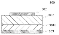
- FIG. 3 shows a preferred example of a semiconductor device using the laminate of the present invention.
- FIG. 3 is an example of a Schottky barrier diode (SBD).
- a Schottky barrier diode (SBD) 300 includes a relatively lightly doped n ⁇ -type semiconductor layer 301a, a relatively heavily doped n + -type semiconductor layer 301b, a Schottky electrode 302 and an ohmic electrode.
- An electrode 303 is provided. Among them, the n ⁇ -type semiconductor layer 301a and the n + -type semiconductor layer 301b use part of the laminate of the present invention.
- the materials of the Schottky electrode 302 and the ohmic electrode 303 may be known electrode materials.
- the electrode materials include aluminum, molybdenum, cobalt, zirconium, tin, niobium, iron, chromium, tantalum, titanium, Metals such as gold, platinum, vanadium, manganese, nickel, copper, hafnium, tungsten, iridium, zinc, indium, palladium, neodymium or silver, or alloys thereof, silver oxide, tin oxide, zinc oxide, rhenium oxide, indium oxide, Metal oxide conductive films such as indium tin oxide (ITO) and indium zinc oxide (IZO), organic conductive compounds such as polyaniline, polythiophene or polypyrrole, or mixtures and laminates thereof.
- ITO indium tin oxide
- IZO indium zinc oxide
- the Schottky electrode 302 and the ohmic electrode 303 can be formed by known means such as vacuum deposition or sputtering. More specifically, for example, when a Schottky electrode is formed using two kinds of metals, a first metal and a second metal, a layer made of the first metal and a layer made of the second metal It can be formed by stacking layers and patterning the layer made of the first metal and the layer made of the second metal using a photolithography technique.
- the Schottky barrier diode (SBD) 300 When a reverse bias is applied to the Schottky barrier diode (SBD) 300, a depletion layer (not shown) spreads in the n ⁇ -type semiconductor layer 301a, resulting in a high withstand voltage SBD. Also, when a forward bias is applied, electrons flow from the ohmic electrode 303 to the Schottky electrode 302 . Therefore, the SBD according to the present invention is excellent for high withstand voltage and large current, has a high switching speed, and is excellent in withstand voltage and reliability.
- FIG. 1 is a diagram for explaining one embodiment of the configuration of a film forming apparatus suitably used for manufacturing the laminate of the present invention.
- the film forming apparatus 100 preferably used for manufacturing the laminate of the present invention includes at least a raw material container 120 for atomizing a film forming raw material solution 121 to form a film forming raw material mist 122, and a film forming raw material mist 122. is supplied to the substrate 130 to form a film on the substrate 130 , a stage 135 on which the substrate 130 is placed, and a heating means 132 for heating the stage 135 .
- the film forming apparatus 100 further includes a carrier gas supply section 111 , and the carrier gas supply section 111 , source container 120 and film forming chamber 131 are connected by pipes 113 and 124 .
- the carrier gas 151 and the film-forming raw material mist 122 are mixed in the raw material container 120 to form a mixture 152 , which is supplied to the film-forming chamber 131 .
- the film-forming raw material solution 121 is not particularly limited as long as it can be misted, and a metal in the form of a complex or salt dissolved or dispersed in an organic solvent or water can be used.
- the metal is not limited as long as it can form a corundum structure as a metal oxide crystal, and examples thereof include Al, Ti, V, Cr, Fe, Co, Ni, Ga, Rh, In, and Ir. .
- Salt forms include, for example, halide salts such as metal chloride salts, metal bromide salts, and metal iodide salts.
- a salt solution in which the metal is dissolved in hydrogen halide such as hydrochloric acid, hydrobromic acid, or hydroiodic acid can also be used.
- the form of the complex includes, for example, an acetylacetone complex, a carbonyl complex, an ammine complex, a hydride complex and the like.
- An acetylacetonate complex can also be formed by mixing acetylacetone with the salt solution.
- the metal content in the film-forming raw material solution is not particularly limited, and can be appropriately set according to the purpose. It is preferably 0.001 mol/L or more and 2 mol/L or less, and more preferably 0.01 mol/L or more and 0.7 mol/L or less.
- the film-forming raw material solution may contain a dopant.
- the dopant is not particularly limited, and includes n-type dopants such as tin, silicon, germanium, titanium, zirconium, vanadium, or niobium, or p-type dopants such as copper, silver, cobalt, iridium, rhodium, magnesium, nickel, and the like. be done.
- Means for atomizing the film-forming raw material solution 121 is not particularly limited as long as it can atomize or dropletize the film-forming raw material solution 121, and may be any known means. is preferred.
- the mist or droplets obtained using ultrasonic waves have an initial velocity of zero and are preferable because they float in the air. Since it is a possible mist, there is no damage due to collision energy, so it is very suitable.
- the droplet size is not particularly limited, and may be droplets of several millimeters, preferably 50 ⁇ m or less, more preferably 0.1 to 10 ⁇ m.
- a plurality of raw material containers 120 may be provided according to the material to be deposited. Further, in this case, the gas mixture 152 supplied from the plurality of raw material containers 120 to the film forming chamber 131 may be independently supplied to the film forming chamber 131, or may be supplied to the pipe 124 or a container for mixing (unnecessary). (illustration) may be separately provided and mixed.
- the raw material container 120 may further include temperature control means (not shown) for directly or indirectly controlling the temperature of the film-forming raw material solution 121 .
- the temperature of the film-forming raw material solution 121 is not particularly limited as long as it can be atomized. . By doing so, the temperature drop on the film formation surface of the substrate 130 is alleviated, and better film formation becomes possible. On the other hand, if the temperature exceeds 90° C., vaporization of the film-forming raw material mist 122 is accelerated, resulting in a decrease in film-forming yield and introduction of defects on the film surface.
- the carrier gas supply unit 111 supplies carrier gas 151 .
- the type of the carrier gas 151 is not particularly limited, and in addition to inert gases such as nitrogen and argon, reducing gases such as air, oxygen, ozone, hydrogen and forming gas can be used. can also be used.
- the flow rate of the carrier gas may be appropriately set depending on the size of the substrate and the size of the film forming chamber, and can be set to, for example, about 0.01 to 100 L/min.
- the carrier gas supply unit 111 may be an air compressor, various gas cylinders, a nitrogen gas separator, or the like, and may be provided with a mechanism for controlling the gas supply flow rate.
- the pipes 113 and 124 are not particularly limited as long as they have sufficient stability against the film-forming raw material solution 121 and the temperature inside and outside the film-forming chamber 131, and are made of quartz, polyethylene, polypropylene, vinyl chloride, or silicon. Common resin pipes such as resin, urethane resin, and fluorine resin can be widely used.
- a pipe from the carrier gas supply unit 111 that does not pass through the raw material container 120 is separately connected to the pipe 124 to further add a diluent gas to the gas mixture 152 to obtain the film-forming raw material mist 122 and the carrier gas. It is also possible to adjust the proportion of gas 151 .
- the flow rate of the diluent gas may be appropriately set, and may be, for example, 0.1 to 10 times/minute of the carrier gas.
- the diluent gas may be supplied to the downstream side of the raw material container 120, for example.
- the same diluent gas as the carrier gas 151 may be used, or a different one may be used.
- the film formation chamber 131 is provided with a supply pipe 134 that is connected to the pipe 124 and that supplies the air-fuel mixture 152 into the film formation chamber 131 .
- a supply pipe 134 for example, quartz, glass, or a resin tube or the like can be used.
- the exhaust gas exhaust port 133 may be provided at a position that does not affect mist supply from the supply pipe 134 .
- the structure, material, and the like of the film formation chamber 131 are not particularly limited, and for example, metal such as aluminum or stainless steel may be used, and quartz, silicon carbide, or glass may be used when film formation is performed at a higher temperature. can be
- a stage 135 is installed at the bottom of the film formation chamber 131 , and the substrate 130 is placed on the stage 135 .
- the stage 135 has a heating means 132, and the substrate 130 is heated by heating the stage 135. As shown in FIG. The heating of the substrate 130 is appropriately adjusted depending on the film-forming raw material mist 122 to be used and the film-forming conditions.
- the material of the stage 135 may be appropriately selected according to the raw material used for film formation and process conditions such as heating temperature. Examples include stainless steel, Hastelloy, brass, copper, graphite, silicon carbide, alumina, and aluminum nitride. is preferably used. A known heating means can be applied to the heating means 132, and resistance heating, electromagnetic induction heating, lamp heating, or the like is preferably used. Further, in order to enhance heat conduction to the substrate 130, the surface roughness Ra of the substrate mounting surface of the stage 135 is 0.5 ⁇ m or less. More preferably, the waviness Wa is 50 ⁇ m or less.
- Ra exceeds 0.5 ⁇ m, the contact area with the substrate 130 is reduced, resulting in deterioration of heat conduction, and the temperature drop of the substrate surface during film formation due to film-forming raw material mist is significant, resulting in deterioration of the crystal orientation of the semiconductor film. decreases.
- the surface roughness Ra may be measured with a measurement length of, for example, 20 ⁇ m or more at one or more arbitrary locations on the mounting surface.
- the smaller the waviness Wa, the better, and although the lower limit is not particularly limited, it can be, for example, 0.5 ⁇ m or more.
- the waviness Wa may be measured on one or more arbitrary straight lines on the mounting surface that are appropriately determined according to the shape of the mounting surface. For example, when the placement surface is circular, the diameter of the circle on two straight lines perpendicular to each other at the center of the circle can be used as the measurement length.
- the surface roughness Ra and waviness Wa are measured using a laser microscope or a confocal microscope such as a stylus method, an atomic force microscope (AFM) method, or an optical interference method, a confocal method, or an image synthesizing method by moving the focal point.
- a laser microscope or a confocal microscope such as a stylus method, an atomic force microscope (AFM) method, or an optical interference method, a confocal method, or an image synthesizing method by moving the focal point.
- AFM atomic force microscope
- the stage 135 may further include a substrate fixing mechanism (not shown).
- a substrate fixing mechanism such as a vacuum chuck, an electrostatic chuck, or a mechanical clamp is preferably used, and preferably a vacuum chuck is used.
- the degree of vacuum in this case is preferably 80 kPa or less in order to stably hold and heat the substrate. The lower the degree of vacuum, the better.
- the degree of vacuum can be set to 1 kPa or more from the viewpoint of cost.
- the present invention provides an apparatus for manufacturing a laminate including a semiconductor film having a corundum type crystal structure, a stage on which the substrate is placed; heating means for heating the substrate; atomizing means for atomizing the film-forming raw material solution; a mixture supplying means for mixing the atomized film-forming raw material solution and a carrier gas and supplying the mixture to the substrate;
- the surface roughness Ra of the contact surface with the substrate on the stage is 0.5 ⁇ m or less.
- the waviness Wa of the contact surface of the stage with the substrate is 50 ⁇ m or less.
- Wa is 50 ⁇ m or less, the contact area with the substrate 130 is increased, thereby improving heat conduction, preventing a significant drop in the temperature of the substrate surface during film formation due to the film-forming raw material mist, and improving the crystal orientation of the semiconductor film. does not decrease.
- the waviness Wa may be measured on one or more arbitrary straight lines on the mounting surface that are appropriately determined according to the shape of the mounting surface. For example, when the placement surface is circular, the diameter of the circle on two straight lines perpendicular to each other at the center of the circle can be used as the measurement length.
- the present invention is a method for manufacturing a laminate comprising a semiconductor film having a corundum type crystal structure, placing the substrate on a stage; heating the substrate; atomizing the film-forming raw material solution; mixing the atomized film-forming raw material solution and a carrier gas to form a mixture; and forming a film by supplying the gas mixture to the substrate,
- the surface roughness Ra of the contact surface of the stage with the substrate and the surface roughness Ra of the contact surface of the substrate with the stage is 0.5 ⁇ m or less.
- a substrate having a surface roughness Ra of 0.5 ⁇ m or less on the second main surface (also referred to as the rear surface) located opposite to the first main surface on which the semiconductor film is formed is used as the substrate.
- the second main surface is the surface of the substrate 130 that contacts the stage 135 mounting surface.
- the shape of the substrate 130 may be any shape as long as it has a first main surface and a second main surface located on the opposite side of the first main surface. It may be cylindrical, prismatic, cylindrical, ring-shaped, or the like, preferably plate-shaped.
- the substrate 130 is not particularly limited as long as it can support the semiconductor film to be formed.
- the material of the substrate 130 is also not particularly limited, and may be a known material, an organic compound, or an inorganic compound.
- a single crystal substrate is particularly preferable, and when a single crystal substrate of GaN, SiC, lithium tantalate, lithium niobate, silicon, sapphire, or ⁇ -type gallium oxide is used, a laminate having better crystal orientation can be obtained. Since it becomes easy to obtain, it is preferable.
- a substrate having a semiconductor film-forming surface area of 5 cm 2 or more, more preferably 10 cm 2 or more, and a thickness of 50 to 5000 ⁇ m, more preferably 100 to 2000 ⁇ m can be suitably used. If the thickness is 50 ⁇ m or more, it is easy to support the semiconductor film, and if it is 5000 ⁇ m or less, the temperature of the substrate surface is not significantly lowered by the film-forming raw material mist, and the crystal orientation of the semiconductor film is not deteriorated.
- the surface roughness Ra of the substrate mounting surface of the stage 135 is set to 0.5 ⁇ m or less. More preferably, the waviness Wa is 50 ⁇ m or less.
- the surface roughness Ra exceeds 0.5 ⁇ m, the contact area with the substrate 130 is reduced, resulting in deterioration of heat conduction, and the temperature of the substrate surface during film formation by the film-forming raw material mist is remarkably lowered, resulting in the formation of a semiconductor film. Crystal orientation deteriorates.
- the surface roughness Ra may be measured with a measurement length of, for example, 20 ⁇ m or more at one or more arbitrary locations on the mounting surface.
- Wa is 50 ⁇ m or less, the contact area with the substrate 130 is increased, thereby improving heat conduction, preventing a significant drop in the temperature of the substrate surface during film formation due to the film-forming raw material mist, and improving the crystal orientation of the semiconductor film. does not decrease.
- the waviness Wa may be measured on one or more arbitrary straight lines on the mounting surface that are appropriately determined according to the shape of the mounting surface.
- the diameter of the circle on two straight lines perpendicular to each other at the center of the circle can be used as the measurement length.
- the surface roughness Ra and waviness Wa are measured using a laser microscope or a confocal microscope such as a stylus method, an atomic force microscope (AFM) method, or an optical interference method, a confocal method, or an image synthesizing method by moving the focal point. Refers to the value obtained by calculating based on JIS B 0601 using the surface shape measurement result by the contact type measurement method.
- the film thickness of the semiconductor film is preferably 1 ⁇ m or more.
- the method of mounting the substrate on the stage is not particularly limited, and a known method can be used.
- the stage 135 may further include a substrate fixing mechanism (not shown).
- a substrate fixing mechanism such as a vacuum chuck, an electrostatic chuck, or a mechanical clamp is preferably used.
- a vacuum chuck it is preferable to use a vacuum chuck.
- the degree of vacuum in this case is preferably 80 kPa or less in order to stably hold and heat the substrate. The lower the degree of vacuum, the better.
- the degree of vacuum can be set to 1 kPa or more from the viewpoint of cost.
- the heating method is not particularly limited, and a known method can be used, but it is particularly preferable to heat the stage. Also, the heating temperature is not particularly limited.
- the method of atomizing the film-forming raw material solution is not particularly limited, and a known method can be used, preferably a method using ultrasonic waves.
- the film-forming raw material solution is not particularly limited as long as it can be atomized, and a solution obtained by dissolving or dispersing a metal in the form of a complex or a salt in an organic solvent or water can be used.
- the method of mixing the atomized film-forming raw material solution and the carrier gas to form the mixture is particularly limited.
- a known method can be used.
- the type of carrier gas is not particularly limited, and in addition to inert gases such as nitrogen and argon, reducing gases such as air, oxygen, ozone, hydrogen and forming gas can also be used, and a plurality of these gases can be mixed and used. can also be used.
- the method of supplying the mixture to the substrate to form a film are not particularly limited, and known methods can be used.
- the present invention is a laminate manufacturing system comprising a semiconductor film having a corundum type crystal structure, a mechanism for placing the substrate on the stage; a mechanism for heating the substrate; a mechanism for atomizing the film-forming raw material solution; a mechanism for mixing the atomized film-forming raw material solution and a carrier gas to form a mixture; a mechanism for supplying the mixture to the substrate to form a film,
- the surface roughness Ra of the contact surface of the stage with the substrate and the surface roughness Ra of the contact surface of the substrate with the stage is 0.5 ⁇ m or less.
- a substrate having a surface roughness Ra of 0.5 ⁇ m or less on the second main surface (also referred to as the rear surface) located opposite to the first main surface on which the semiconductor film is formed is used as the substrate.
- the second main surface is the surface of the substrate 130 that contacts the stage 135 mounting surface.
- the shape of the substrate 130 may be any shape as long as it has a first main surface and a second main surface located on the opposite side of the first main surface. It may be cylindrical, prismatic, cylindrical, ring-shaped, or the like, preferably plate-shaped.
- the substrate 130 is not particularly limited as long as it can support the semiconductor film to be formed.
- the material of the substrate 130 is also not particularly limited, and may be a known material, an organic compound, or an inorganic compound.
- a single crystal substrate is particularly preferable, and when a single crystal substrate of GaN, SiC, lithium tantalate, lithium niobate, silicon, sapphire, or ⁇ -type gallium oxide is used, a laminate having better crystal orientation can be obtained. Since it becomes easy to obtain, it is preferable.
- a substrate having a semiconductor film-forming surface area of 5 cm 2 or more, more preferably 10 cm 2 or more, and a thickness of 50 to 5000 ⁇ m, more preferably 100 to 2000 ⁇ m can be suitably used. If the thickness is 50 ⁇ m or more, it is easy to support the semiconductor film, and if it is 5000 ⁇ m or less, the temperature of the substrate surface is not significantly lowered by the film-forming raw material mist, and the crystal orientation of the semiconductor film is not deteriorated.
- the surface roughness Ra of the substrate mounting surface of the stage 135 is set to 0.5 ⁇ m or less. More preferably, the waviness Wa is 50 ⁇ m or less.
- the surface roughness Ra exceeds 0.5 ⁇ m, the contact area with the substrate 130 is reduced, resulting in deterioration of heat conduction, and the temperature of the substrate surface during film formation by the film-forming raw material mist is remarkably lowered, resulting in the formation of a semiconductor film. Crystal orientation deteriorates.
- the surface roughness Ra may be measured with a measurement length of, for example, 20 ⁇ m or more at one or more arbitrary locations on the mounting surface.
- Wa is 50 ⁇ m or less, the contact area with the substrate 130 is increased, thereby improving heat conduction, preventing a significant drop in the temperature of the substrate surface during film formation due to the film-forming raw material mist, and improving the crystal orientation of the semiconductor film. does not decrease.
- the waviness Wa may be measured on one or more arbitrary straight lines on the mounting surface that are appropriately determined according to the shape of the mounting surface.
- the diameter of the circle on two straight lines perpendicular to each other at the center of the circle can be used as the measurement length.
- the surface roughness Ra and waviness Wa are measured using a laser microscope or a confocal microscope such as a stylus method, an atomic force microscope (AFM) method, or an optical interference method, a confocal method, or an image synthesizing method by moving the focal point. Refers to the value obtained by calculating based on JIS B 0601 using the surface shape measurement result by the contact type measurement method.
- the film thickness of the semiconductor film is preferably 1 ⁇ m or more.
- the method for mounting the substrate on the stage is not particularly limited, and a known method can be used.
- the stage 135 may further include a substrate fixing mechanism (not shown).
- a substrate fixing mechanism such as a vacuum chuck, an electrostatic chuck, or a mechanical clamp is preferably used.
- a vacuum chuck it is preferable to use a vacuum chuck.
- the degree of vacuum in this case is preferably 80 kPa or less in order to stably hold and heat the substrate. The lower the degree of vacuum, the better.
- the degree of vacuum can be set to 1 kPa or more from the viewpoint of cost.
- the heating method is not particularly limited, and a known method can be used, but it is particularly preferable to heat the stage. Also, the heating temperature is not particularly limited.
- the method for atomizing the film-forming raw material solution is not particularly limited, and a known method can be used, preferably a method using ultrasonic waves.
- the film-forming raw material solution is not particularly limited as long as it can be atomized, and a solution obtained by dissolving or dispersing a metal in the form of a complex or a salt in an organic solvent or water can be used.
- the method of mixing the atomized film-forming raw material solution and the carrier gas to form the mixture is particularly limited.
- a known method can be used.
- the type of carrier gas is not particularly limited, and in addition to inert gases such as nitrogen and argon, reducing gases such as air, oxygen, ozone, hydrogen and forming gas can also be used, and a plurality of these gases can be mixed and used. can also be used.
- the method of supplying the mixture to the substrate and the method of forming the film are not particularly limited, and known methods can be used.
- Example 1 A film of ⁇ -gallium oxide was formed using the film forming apparatus shown in FIG.
- an atomizing device having a raw material container made of quartz and two ultrasonic vibrators (frequency: 2.4 MHz) was used.
- the film forming chamber was made of quartz, and had a supply pipe made of quartz and a hot plate made of silicon carbide as a stage.
- the surface roughness Ra of the substrate mounting surface of the stage was 0.05 ⁇ m, and the waviness Wa was 4.3 ⁇ m.
- a gas cylinder filled with nitrogen gas was used to supply the carrier gas.
- the gas cylinder and the film forming atomization device were connected with a urethane resin tube, and the film forming atomization device and the supply pipe were connected with a quartz pipe.
- gallium acetylacetonate was mixed at a ratio of 0.1 mol/L with a solution in which 1% by volume of 34% hydrochloric acid was added to pure water, and the mixture was stirred with a stirrer for 60 minutes to dissolve the mixture, and the film-forming raw material was mixed. solution.
- the film-forming raw material solution is filled in the raw material container, and ultrasonic vibration is propagated to the film-forming raw material solution in the raw material container through the ultrasonic wave propagating water by the ultrasonic oscillator, so that the film-forming raw material solution is misted. turned into a mist.
- the temperature of the ultrasonic propagating water was adjusted, and the raw material solution for film formation was kept at 35°C.
- a c-plane sapphire substrate (substrate) having a diameter of 10 cm (4 inches), a thickness of 0.6 mm, a back surface roughness Ra of 0.05 ⁇ m, and a waviness Wa of 1.9 ⁇ m was placed on the mounting surface of the stage.
- the pressure was reduced to 20 kPa with a vacuum pump and fixed. After that, the stage was heated so that the surface temperature of the stage reached 500.degree. Next, nitrogen gas was added to the raw material container at a flow rate of 5 L/min, and a mixture of mist and nitrogen gas was supplied to the film forming chamber for 30 minutes to form a film. Immediately after this, the supply of nitrogen gas was stopped, and the supply of the air-fuel mixture to the film forming chamber was stopped. The crystal layer of the produced laminate was confirmed to be ⁇ -Ga 2 O 3 by X-ray diffraction measurement. After that, the half-value width was evaluated by rocking curve measurement of X-ray diffraction. Also, the film thickness of the crystal layer was measured by ellipsometry.
- Example 2 Film formation was performed in the same manner as in Example 1 except that the surface roughness Ra of the substrate mounting surface of the stage was set to 0.45 ⁇ m and the surface roughness Ra of the rear surface of the substrate was set to 0.41 ⁇ m.
- the crystal layer of the produced laminate was confirmed to be ⁇ -Ga 2 O 3 by X-ray diffraction measurement. Thereafter, the half width and film thickness of the crystal layer were evaluated in the same manner as in Example 1.
- Example 3 A film was formed in the same manner as in Example 2, except that the air-fuel mixture was supplied to the film forming chamber for 150 minutes.
- the crystal layer of the produced laminate was confirmed to be ⁇ -Ga 2 O 3 by X-ray diffraction measurement. Thereafter, the half width and film thickness of the crystal layer were evaluated in the same manner as in Example 1.
- Example 4 Film formation was performed in the same manner as in Example 1, except that the degree of vacuum for fixing the substrate was set to 75 kPa.
- the crystal layer of the produced laminate was confirmed to be ⁇ -Ga 2 O 3 by X-ray diffraction measurement. Thereafter, the half width and film thickness of the crystal layer were evaluated in the same manner as in Example 1.
- Example 1 A film was formed in the same manner as in Example 1 except that the surface roughness Ra of the substrate mounting surface of the stage was set to 0.60 ⁇ m.
- the crystal layer of the produced laminate was confirmed to be ⁇ -Ga 2 O 3 by X-ray diffraction measurement. Thereafter, the half width and film thickness of the crystal layer were evaluated in the same manner as in Example 1.
- Example 2 A film was formed in the same manner as in Example 1 except that the surface roughness Ra of the back surface of the substrate was set to 0.62 ⁇ m.
- the crystal layer of the produced laminate was confirmed to be ⁇ -Ga 2 O 3 by X-ray diffraction measurement. Thereafter, the half width and film thickness of the crystal layer were evaluated in the same manner as in Example 1.
- Example 3 Film formation was carried out in the same manner as in Example 1, except that the surface roughness Ra of the back surface of the substrate was set to 0.62 ⁇ m, and the mixture gas supply time to the film formation chamber was set to 150 minutes. The crystal layer of the produced laminate was confirmed to be ⁇ -Ga 2 O 3 by X-ray diffraction measurement. Thereafter, the half width and film thickness of the crystal layer were evaluated in the same manner as in Example 1.
- Example 4 A film was formed in the same manner as in Example 1 except that the surface roughness Ra of the back surface of the substrate was set to 0.62 ⁇ m and the degree of vacuum for fixing the substrate was set to 95 kPa.
- the crystal layer of the produced laminate was confirmed to be ⁇ -Ga 2 O 3 by X-ray diffraction measurement. Thereafter, the half width and film thickness of the crystal layer were evaluated in the same manner as in Example 1.
- Example 5 A film was formed in the same manner as in Example 1, except that the waviness Wa on the back surface of the substrate was set to 45.8 ⁇ m.
- the crystal layer of the produced laminate was confirmed to be ⁇ -Ga 2 O 3 by X-ray diffraction measurement. Thereafter, the half width and film thickness of the crystal layer were evaluated in the same manner as in Example 1.
- Example 6 A film was formed in the same manner as in Example 1, except that the waviness Wa of the stage mounting surface was set to 48.2 ⁇ m.
- the crystal layer of the produced laminate was confirmed to be ⁇ -Ga 2 O 3 by X-ray diffraction measurement. Thereafter, the half width and film thickness of the crystal layer were evaluated in the same manner as in Example 1.
- Example 7 Film formation was performed in the same manner as in Example 1, except that the waviness Wa of the back surface of the substrate was set to 47.7 ⁇ m and the waviness Wa of the stage mounting surface was set to 48.2 ⁇ m.
- the crystal layer of the produced laminate was confirmed to be ⁇ -Ga 2 O 3 by X-ray diffraction measurement. Thereafter, the half width and film thickness of the crystal layer were evaluated in the same manner as in Example 1.
- Example 8 A film was formed in the same manner as in Example 1, except that the waviness Wa of the stage mounting surface was set to 59.7 ⁇ m.
- the crystal layer of the produced laminate was confirmed to be ⁇ -Ga 2 O 3 by X-ray diffraction measurement. Thereafter, the half width and film thickness of the crystal layer were evaluated in the same manner as in Example 1.
- Example 9 A film was formed in the same manner as in Example 1, except that the waviness Wa on the back surface of the substrate was set to 52.1 ⁇ m.
- the crystal layer of the produced laminate was confirmed to be ⁇ -Ga 2 O 3 by X-ray diffraction measurement. Thereafter, the half width and film thickness of the crystal layer were evaluated in the same manner as in Example 1.
- Table 1 shows the film thicknesses and rocking curve half-value widths of the crystal layers obtained in Examples 1-9 and Comparative Examples 1-4.
- the film deposition apparatus achieved both a film thickness exceeding 1 ⁇ m and a low half width (high crystal orientation). It can be seen that it is an excellent one that can produce a quality crystal layer (semiconductor film).
- the half width increased and the growth rate increased (the crystal orientation increased. decrease) was observed. This is considered to be the result of abnormal film growth caused by a temperature drop on the film surface.
- the present invention is not limited to the above embodiments.
- the above-described embodiment is an example, and any device having substantially the same configuration as the technical idea described in the claims of the present invention and exhibiting the same effect is the present invention. included in the technical scope of
Landscapes
- Chemical & Material Sciences (AREA)
- Engineering & Computer Science (AREA)
- Materials Engineering (AREA)
- Metallurgy (AREA)
- Organic Chemistry (AREA)
- General Chemical & Material Sciences (AREA)
- Chemical Kinetics & Catalysis (AREA)
- Mechanical Engineering (AREA)
- Crystallography & Structural Chemistry (AREA)
- Inorganic Chemistry (AREA)
- Dispersion Chemistry (AREA)
- Crystals, And After-Treatments Of Crystals (AREA)
- Control Of Motors That Do Not Use Commutators (AREA)
- Structures Or Materials For Encapsulating Or Coating Semiconductor Devices Or Solid State Devices (AREA)
- Ceramic Capacitors (AREA)
- Chemical Vapour Deposition (AREA)
- Liquid Deposition Of Substances Of Which Semiconductor Devices Are Composed (AREA)
Priority Applications (5)
| Application Number | Priority Date | Filing Date | Title |
|---|---|---|---|
| JP2023512978A JP7614336B2 (ja) | 2021-04-07 | 2022-03-30 | 積層体の製造方法、積層体の製造装置、積層体及び半導体装置 |
| CN202280026055.2A CN117098879A (zh) | 2021-04-07 | 2022-03-30 | 层叠体的制造方法、层叠体的制造装置、层叠体以及半导体装置 |
| EP22784605.2A EP4321657A4 (en) | 2021-04-07 | 2022-03-30 | METHOD FOR MANUFACTURING LAMINATED BODY, DEVICE FOR MANUFACTURING LAMINATED BODY, LAMINATED BODY AND SEMICONDUCTIVE DEVICE |
| US18/285,406 US20240177993A1 (en) | 2021-04-07 | 2022-03-30 | Method for producing laminate, producing apparatus for laminate, laminate, and semiconductor device |
| KR1020237033715A KR20230165241A (ko) | 2021-04-07 | 2022-03-30 | 적층체의 제조방법, 적층체의 제조장치, 적층체 및 반도체장치 |
Applications Claiming Priority (2)
| Application Number | Priority Date | Filing Date | Title |
|---|---|---|---|
| JP2021065332 | 2021-04-07 | ||
| JP2021-065332 | 2021-04-07 |
Publications (1)
| Publication Number | Publication Date |
|---|---|
| WO2022215621A1 true WO2022215621A1 (ja) | 2022-10-13 |
Family
ID=83545528
Family Applications (1)
| Application Number | Title | Priority Date | Filing Date |
|---|---|---|---|
| PCT/JP2022/015913 Ceased WO2022215621A1 (ja) | 2021-04-07 | 2022-03-30 | 積層体の製造方法、積層体の製造装置、積層体及び半導体装置 |
Country Status (7)
| Country | Link |
|---|---|
| US (1) | US20240177993A1 (https=) |
| EP (1) | EP4321657A4 (https=) |
| JP (1) | JP7614336B2 (https=) |
| KR (1) | KR20230165241A (https=) |
| CN (2) | CN218146932U (https=) |
| TW (2) | TWM633935U (https=) |
| WO (1) | WO2022215621A1 (https=) |
Cited By (1)
| Publication number | Priority date | Publication date | Assignee | Title |
|---|---|---|---|---|
| JPWO2024043134A1 (https=) * | 2022-08-26 | 2024-02-29 |
Citations (9)
| Publication number | Priority date | Publication date | Assignee | Title |
|---|---|---|---|---|
| JP2006290676A (ja) * | 2005-04-11 | 2006-10-26 | Hitachi Cable Ltd | Iii−v族窒化物半導体基板およびその製造方法 |
| JP2012036013A (ja) * | 2010-08-03 | 2012-02-23 | Tokyo Univ Of Agriculture & Technology | 結晶成長装置 |
| JP2013028480A (ja) | 2011-07-27 | 2013-02-07 | Kochi Univ Of Technology | ドーパントを添加した結晶性の高い導電性α型酸化ガリウム薄膜およびその生成方法 |
| JP2014103364A (ja) * | 2012-11-22 | 2014-06-05 | Toyoda Gosei Co Ltd | 化合物半導体の製造装置およびウェハ保持体 |
| WO2014091968A1 (ja) * | 2012-12-14 | 2014-06-19 | 日本碍子株式会社 | 単結晶製造方法、及び当該方法によって製造される単結晶 |
| JP2015039033A (ja) * | 2006-12-28 | 2015-02-26 | サン−ゴバン セラミックス アンド プラスティクス,インコーポレイティド | サファイア基板 |
| JP2020107636A (ja) | 2018-12-26 | 2020-07-09 | 株式会社Flosfia | 結晶性酸化物膜 |
| JP2020174153A (ja) * | 2019-04-12 | 2020-10-22 | 信越化学工業株式会社 | 酸化ガリウム半導体膜の製造方法 |
| WO2020217564A1 (ja) * | 2019-04-24 | 2020-10-29 | 日本碍子株式会社 | 半導体膜 |
Family Cites Families (9)
| Publication number | Priority date | Publication date | Assignee | Title |
|---|---|---|---|---|
| US20110049779A1 (en) * | 2009-08-28 | 2011-03-03 | Applied Materials, Inc. | Substrate carrier design for improved photoluminescence uniformity |
| US9564320B2 (en) * | 2010-06-18 | 2017-02-07 | Soraa, Inc. | Large area nitride crystal and method for making it |
| EP2927934B1 (en) * | 2014-03-31 | 2017-07-05 | Flosfia Inc. | Crystalline multilayer structure and semiconductor device |
| EP2933825B1 (en) * | 2014-03-31 | 2017-07-05 | Flosfia Inc. | Crystalline multilayer structure and semiconductor device |
| CN115714130A (zh) * | 2016-12-05 | 2023-02-24 | 环球晶圆股份有限公司 | 高电阻率绝缘体上硅结构及其制造方法 |
| CN110785682B (zh) * | 2017-05-24 | 2022-08-26 | 斯伦贝谢技术有限公司 | 对井下多维测量结果的快速测量和解释 |
| DE112019003987T5 (de) * | 2018-08-09 | 2021-04-22 | Shin-Etsu Chemical Co., Ltd. | VERFAHREN ZUR HERSTELLUNG EINES GaN-LAMINATSUBSTRATS |
| JP7681039B2 (ja) * | 2020-10-08 | 2025-05-21 | 日本碍子株式会社 | 酸化ガリウム単結晶粒子及びその製法 |
| TWM633282U (zh) * | 2021-04-28 | 2022-10-21 | 日商信越化學工業股份有限公司 | 積層結構體、半導體裝置以及積層結構體的製造系統 |
-
2022
- 2022-03-23 TW TW111202886U patent/TWM633935U/zh unknown
- 2022-03-23 TW TW111110817A patent/TW202332813A/zh unknown
- 2022-03-30 CN CN202220709419.4U patent/CN218146932U/zh active Active
- 2022-03-30 JP JP2023512978A patent/JP7614336B2/ja active Active
- 2022-03-30 EP EP22784605.2A patent/EP4321657A4/en active Pending
- 2022-03-30 KR KR1020237033715A patent/KR20230165241A/ko active Pending
- 2022-03-30 WO PCT/JP2022/015913 patent/WO2022215621A1/ja not_active Ceased
- 2022-03-30 US US18/285,406 patent/US20240177993A1/en active Pending
- 2022-03-30 CN CN202280026055.2A patent/CN117098879A/zh active Pending
Patent Citations (9)
| Publication number | Priority date | Publication date | Assignee | Title |
|---|---|---|---|---|
| JP2006290676A (ja) * | 2005-04-11 | 2006-10-26 | Hitachi Cable Ltd | Iii−v族窒化物半導体基板およびその製造方法 |
| JP2015039033A (ja) * | 2006-12-28 | 2015-02-26 | サン−ゴバン セラミックス アンド プラスティクス,インコーポレイティド | サファイア基板 |
| JP2012036013A (ja) * | 2010-08-03 | 2012-02-23 | Tokyo Univ Of Agriculture & Technology | 結晶成長装置 |
| JP2013028480A (ja) | 2011-07-27 | 2013-02-07 | Kochi Univ Of Technology | ドーパントを添加した結晶性の高い導電性α型酸化ガリウム薄膜およびその生成方法 |
| JP2014103364A (ja) * | 2012-11-22 | 2014-06-05 | Toyoda Gosei Co Ltd | 化合物半導体の製造装置およびウェハ保持体 |
| WO2014091968A1 (ja) * | 2012-12-14 | 2014-06-19 | 日本碍子株式会社 | 単結晶製造方法、及び当該方法によって製造される単結晶 |
| JP2020107636A (ja) | 2018-12-26 | 2020-07-09 | 株式会社Flosfia | 結晶性酸化物膜 |
| JP2020174153A (ja) * | 2019-04-12 | 2020-10-22 | 信越化学工業株式会社 | 酸化ガリウム半導体膜の製造方法 |
| WO2020217564A1 (ja) * | 2019-04-24 | 2020-10-29 | 日本碍子株式会社 | 半導体膜 |
Non-Patent Citations (1)
| Title |
|---|
| See also references of EP4321657A4 |
Cited By (2)
| Publication number | Priority date | Publication date | Assignee | Title |
|---|---|---|---|---|
| JPWO2024043134A1 (https=) * | 2022-08-26 | 2024-02-29 | ||
| WO2024043134A1 (ja) * | 2022-08-26 | 2024-02-29 | 信越化学工業株式会社 | 成膜方法、成膜装置、サセプター、及びα-酸化ガリウム膜 |
Also Published As
| Publication number | Publication date |
|---|---|
| KR20230165241A (ko) | 2023-12-05 |
| JP7614336B2 (ja) | 2025-01-15 |
| EP4321657A4 (en) | 2026-01-21 |
| US20240177993A1 (en) | 2024-05-30 |
| EP4321657A1 (en) | 2024-02-14 |
| TWM633935U (zh) | 2022-11-11 |
| TW202332813A (zh) | 2023-08-16 |
| CN117098879A (zh) | 2023-11-21 |
| CN218146932U (zh) | 2022-12-27 |
| JPWO2022215621A1 (https=) | 2022-10-13 |
Similar Documents
| Publication | Publication Date | Title |
|---|---|---|
| JP6573207B2 (ja) | 半導体装置 | |
| JP7220257B2 (ja) | 積層体、半導体装置、ミストcvd装置及び成膜方法 | |
| JP2019036737A (ja) | 剥離方法 | |
| JP7614336B2 (ja) | 積層体の製造方法、積層体の製造装置、積層体及び半導体装置 | |
| JP2025102965A (ja) | 積層構造体、半導体装置及び下地基板 | |
| JP7592131B2 (ja) | 積層構造体 | |
| JP2021038118A (ja) | 積層構造体及び半導体装置並びに積層構造体の製造方法 | |
| JP7078581B2 (ja) | 積層構造体及び半導体装置並びに積層構造体の製造方法 | |
| CN114302982A (zh) | 层叠结构体及层叠结构体的制造方法 | |
| JP2021038116A (ja) | 積層構造体及び半導体装置並びに積層構造体の製造方法 |
Legal Events
| Date | Code | Title | Description |
|---|---|---|---|
| 121 | Ep: the epo has been informed by wipo that ep was designated in this application |
Ref document number: 22784605 Country of ref document: EP Kind code of ref document: A1 |
|
| WWE | Wipo information: entry into national phase |
Ref document number: 2023512978 Country of ref document: JP |
|
| WWE | Wipo information: entry into national phase |
Ref document number: 202280026055.2 Country of ref document: CN |
|
| WWE | Wipo information: entry into national phase |
Ref document number: 202347065448 Country of ref document: IN |
|
| WWE | Wipo information: entry into national phase |
Ref document number: 18285406 Country of ref document: US |
|
| WWE | Wipo information: entry into national phase |
Ref document number: 2022784605 Country of ref document: EP |
|
| NENP | Non-entry into the national phase |
Ref country code: DE |
|
| ENP | Entry into the national phase |
Ref document number: 2022784605 Country of ref document: EP Effective date: 20231107 |