WO2020217564A1 - 半導体膜 - Google Patents
半導体膜 Download PDFInfo
- Publication number
- WO2020217564A1 WO2020217564A1 PCT/JP2019/035514 JP2019035514W WO2020217564A1 WO 2020217564 A1 WO2020217564 A1 WO 2020217564A1 JP 2019035514 W JP2019035514 W JP 2019035514W WO 2020217564 A1 WO2020217564 A1 WO 2020217564A1
- Authority
- WO
- WIPO (PCT)
- Prior art keywords
- semiconductor film
- film
- substrate
- layer
- plane
- Prior art date
Links
- 239000004065 semiconductor Substances 0.000 title claims abstract description 151
- 239000013078 crystal Substances 0.000 claims abstract description 94
- 230000007547 defect Effects 0.000 claims abstract description 35
- 239000006104 solid solution Substances 0.000 claims abstract description 24
- 229910005191 Ga 2 O 3 Inorganic materials 0.000 claims description 69
- 229910052593 corundum Inorganic materials 0.000 claims description 11
- 239000010431 corundum Substances 0.000 claims description 11
- 239000002019 doping agent Substances 0.000 claims description 9
- 229910052800 carbon group element Inorganic materials 0.000 claims description 7
- QZQVBEXLDFYHSR-UHFFFAOYSA-N gallium(III) oxide Inorganic materials O=[Ga]O[Ga]=O QZQVBEXLDFYHSR-UHFFFAOYSA-N 0.000 abstract description 3
- 229910005979 Ge2O3 Inorganic materials 0.000 abstract 1
- 239000010408 film Substances 0.000 description 232
- 239000000758 substrate Substances 0.000 description 184
- 239000010410 layer Substances 0.000 description 111
- 238000000034 method Methods 0.000 description 70
- 229910052594 sapphire Inorganic materials 0.000 description 65
- 239000010980 sapphire Substances 0.000 description 65
- 230000015572 biosynthetic process Effects 0.000 description 49
- 239000007789 gas Substances 0.000 description 43
- 239000002994 raw material Substances 0.000 description 43
- 239000002243 precursor Substances 0.000 description 39
- 239000000463 material Substances 0.000 description 36
- 238000005259 measurement Methods 0.000 description 33
- 238000010438 heat treatment Methods 0.000 description 32
- 239000002131 composite material Substances 0.000 description 31
- 238000005229 chemical vapour deposition Methods 0.000 description 21
- 239000000443 aerosol Substances 0.000 description 20
- 229910052760 oxygen Inorganic materials 0.000 description 17
- 239000000843 powder Substances 0.000 description 15
- 229910052733 gallium Inorganic materials 0.000 description 14
- 239000012159 carrier gas Substances 0.000 description 13
- 239000003595 mist Substances 0.000 description 13
- VYPSYNLAJGMNEJ-UHFFFAOYSA-N silicon dioxide Inorganic materials O=[Si]=O VYPSYNLAJGMNEJ-UHFFFAOYSA-N 0.000 description 13
- 239000010453 quartz Substances 0.000 description 12
- 238000002441 X-ray diffraction Methods 0.000 description 11
- QVGXLLKOCUKJST-UHFFFAOYSA-N atomic oxygen Chemical compound [O] QVGXLLKOCUKJST-UHFFFAOYSA-N 0.000 description 11
- 239000002346 layers by function Substances 0.000 description 11
- 238000004519 manufacturing process Methods 0.000 description 11
- 239000001301 oxygen Substances 0.000 description 11
- 238000005498 polishing Methods 0.000 description 11
- 238000011156 evaluation Methods 0.000 description 10
- 238000000465 moulding Methods 0.000 description 10
- 239000000243 solution Substances 0.000 description 10
- -1 vacuum Substances 0.000 description 10
- 238000000151 deposition Methods 0.000 description 8
- 230000008021 deposition Effects 0.000 description 8
- 238000002248 hydride vapour-phase epitaxy Methods 0.000 description 8
- 238000002360 preparation method Methods 0.000 description 8
- 238000003917 TEM image Methods 0.000 description 7
- 239000012298 atmosphere Substances 0.000 description 7
- 230000015556 catabolic process Effects 0.000 description 7
- 238000006243 chemical reaction Methods 0.000 description 7
- 230000005684 electric field Effects 0.000 description 7
- 238000000227 grinding Methods 0.000 description 7
- 239000002184 metal Substances 0.000 description 7
- 229910052751 metal Inorganic materials 0.000 description 7
- 239000000203 mixture Substances 0.000 description 7
- VEXZGXHMUGYJMC-UHFFFAOYSA-N Hydrochloric acid Chemical compound Cl VEXZGXHMUGYJMC-UHFFFAOYSA-N 0.000 description 6
- 150000004820 halides Chemical class 0.000 description 6
- 238000002347 injection Methods 0.000 description 6
- 239000007924 injection Substances 0.000 description 6
- 239000012071 phase Substances 0.000 description 6
- 229910018072 Al 2 O 3 Inorganic materials 0.000 description 5
- IJGRMHOSHXDMSA-UHFFFAOYSA-N Atomic nitrogen Chemical compound N#N IJGRMHOSHXDMSA-UHFFFAOYSA-N 0.000 description 5
- ATJFFYVFTNAWJD-UHFFFAOYSA-N Tin Chemical compound [Sn] ATJFFYVFTNAWJD-UHFFFAOYSA-N 0.000 description 5
- 229910052782 aluminium Inorganic materials 0.000 description 5
- 239000012895 dilution Substances 0.000 description 5
- 238000010790 dilution Methods 0.000 description 5
- 238000013507 mapping Methods 0.000 description 5
- 230000000149 penetrating effect Effects 0.000 description 5
- 238000004544 sputter deposition Methods 0.000 description 5
- GYHNNYVSQQEPJS-UHFFFAOYSA-N Gallium Chemical compound [Ga] GYHNNYVSQQEPJS-UHFFFAOYSA-N 0.000 description 4
- 230000005540 biological transmission Effects 0.000 description 4
- 229910052804 chromium Inorganic materials 0.000 description 4
- 238000010304 firing Methods 0.000 description 4
- 229910052736 halogen Inorganic materials 0.000 description 4
- 150000002367 halogens Chemical class 0.000 description 4
- 238000012545 processing Methods 0.000 description 4
- 238000012360 testing method Methods 0.000 description 4
- 229910000859 α-Fe Inorganic materials 0.000 description 4
- ZVYYAYJIGYODSD-LNTINUHCSA-K (z)-4-bis[[(z)-4-oxopent-2-en-2-yl]oxy]gallanyloxypent-3-en-2-one Chemical compound [Ga+3].C\C([O-])=C\C(C)=O.C\C([O-])=C\C(C)=O.C\C([O-])=C\C(C)=O ZVYYAYJIGYODSD-LNTINUHCSA-K 0.000 description 3
- 239000006061 abrasive grain Substances 0.000 description 3
- 230000001133 acceleration Effects 0.000 description 3
- 239000000919 ceramic Substances 0.000 description 3
- 238000005516 engineering process Methods 0.000 description 3
- 238000001027 hydrothermal synthesis Methods 0.000 description 3
- 229910052757 nitrogen Inorganic materials 0.000 description 3
- 238000005245 sintering Methods 0.000 description 3
- 239000007790 solid phase Substances 0.000 description 3
- 238000000992 sputter etching Methods 0.000 description 3
- 239000000126 substance Substances 0.000 description 3
- GZNAASVAJNXPPW-UHFFFAOYSA-M tin(4+) chloride dihydrate Chemical compound O.O.[Cl-].[Sn+4] GZNAASVAJNXPPW-UHFFFAOYSA-M 0.000 description 3
- FWPIDFUJEMBDLS-UHFFFAOYSA-L tin(II) chloride dihydrate Substances O.O.Cl[Sn]Cl FWPIDFUJEMBDLS-UHFFFAOYSA-L 0.000 description 3
- OKTJSMMVPCPJKN-UHFFFAOYSA-N Carbon Chemical compound [C] OKTJSMMVPCPJKN-UHFFFAOYSA-N 0.000 description 2
- 239000007864 aqueous solution Substances 0.000 description 2
- 238000005219 brazing Methods 0.000 description 2
- 229910052799 carbon Inorganic materials 0.000 description 2
- XOYLJNJLGBYDTH-UHFFFAOYSA-M chlorogallium Chemical compound [Ga]Cl XOYLJNJLGBYDTH-UHFFFAOYSA-M 0.000 description 2
- 238000000280 densification Methods 0.000 description 2
- 239000010432 diamond Substances 0.000 description 2
- 229910003460 diamond Inorganic materials 0.000 description 2
- 238000009792 diffusion process Methods 0.000 description 2
- AJNVQOSZGJRYEI-UHFFFAOYSA-N digallium;oxygen(2-) Chemical compound [O-2].[O-2].[O-2].[Ga+3].[Ga+3] AJNVQOSZGJRYEI-UHFFFAOYSA-N 0.000 description 2
- 239000003085 diluting agent Substances 0.000 description 2
- 238000001887 electron backscatter diffraction Methods 0.000 description 2
- 239000010419 fine particle Substances 0.000 description 2
- 238000009499 grossing Methods 0.000 description 2
- 239000012433 hydrogen halide Substances 0.000 description 2
- 229910000039 hydrogen halide Inorganic materials 0.000 description 2
- 229910052738 indium Inorganic materials 0.000 description 2
- 239000011261 inert gas Substances 0.000 description 2
- 150000002500 ions Chemical class 0.000 description 2
- 230000008707 rearrangement Effects 0.000 description 2
- 239000002002 slurry Substances 0.000 description 2
- 238000005476 soldering Methods 0.000 description 2
- 238000005092 sublimation method Methods 0.000 description 2
- 239000002344 surface layer Substances 0.000 description 2
- 238000001947 vapour-phase growth Methods 0.000 description 2
- XLYOFNOQVPJJNP-UHFFFAOYSA-N water Substances O XLYOFNOQVPJJNP-UHFFFAOYSA-N 0.000 description 2
- 239000004593 Epoxy Substances 0.000 description 1
- XUIMIQQOPSSXEZ-UHFFFAOYSA-N Silicon Chemical compound [Si] XUIMIQQOPSSXEZ-UHFFFAOYSA-N 0.000 description 1
- 229910021626 Tin(II) chloride Inorganic materials 0.000 description 1
- 239000000654 additive Substances 0.000 description 1
- 239000000853 adhesive Substances 0.000 description 1
- 230000001070 adhesive effect Effects 0.000 description 1
- 239000012790 adhesive layer Substances 0.000 description 1
- PNEYBMLMFCGWSK-UHFFFAOYSA-N aluminium oxide Inorganic materials [O-2].[O-2].[O-2].[Al+3].[Al+3] PNEYBMLMFCGWSK-UHFFFAOYSA-N 0.000 description 1
- 238000004458 analytical method Methods 0.000 description 1
- 239000011230 binding agent Substances 0.000 description 1
- 229910001417 caesium ion Inorganic materials 0.000 description 1
- 238000005266 casting Methods 0.000 description 1
- 239000011248 coating agent Substances 0.000 description 1
- 238000000576 coating method Methods 0.000 description 1
- 239000008119 colloidal silica Substances 0.000 description 1
- 150000001875 compounds Chemical class 0.000 description 1
- 229910052802 copper Inorganic materials 0.000 description 1
- 238000001514 detection method Methods 0.000 description 1
- 229910001873 dinitrogen Inorganic materials 0.000 description 1
- 239000002270 dispersing agent Substances 0.000 description 1
- 239000002612 dispersion medium Substances 0.000 description 1
- 238000009826 distribution Methods 0.000 description 1
- 238000007606 doctor blade method Methods 0.000 description 1
- 238000001125 extrusion Methods 0.000 description 1
- 229910001195 gallium oxide Inorganic materials 0.000 description 1
- 238000010574 gas phase reaction Methods 0.000 description 1
- 229910052732 germanium Inorganic materials 0.000 description 1
- GNPVGFCGXDBREM-UHFFFAOYSA-N germanium atom Chemical compound [Ge] GNPVGFCGXDBREM-UHFFFAOYSA-N 0.000 description 1
- 229910002804 graphite Inorganic materials 0.000 description 1
- 239000010439 graphite Substances 0.000 description 1
- 238000002017 high-resolution X-ray diffraction Methods 0.000 description 1
- 238000007731 hot pressing Methods 0.000 description 1
- 229910052739 hydrogen Inorganic materials 0.000 description 1
- 150000002484 inorganic compounds Chemical class 0.000 description 1
- 229910010272 inorganic material Inorganic materials 0.000 description 1
- 238000010884 ion-beam technique Methods 0.000 description 1
- 238000005304 joining Methods 0.000 description 1
- 239000012528 membrane Substances 0.000 description 1
- 238000002488 metal-organic chemical vapour deposition Methods 0.000 description 1
- 238000003801 milling Methods 0.000 description 1
- 229910052750 molybdenum Inorganic materials 0.000 description 1
- 239000012299 nitrogen atmosphere Substances 0.000 description 1
- 239000002245 particle Substances 0.000 description 1
- 230000000737 periodic effect Effects 0.000 description 1
- 230000002093 peripheral effect Effects 0.000 description 1
- 230000000704 physical effect Effects 0.000 description 1
- 238000005268 plasma chemical vapour deposition Methods 0.000 description 1
- 239000004014 plasticizer Substances 0.000 description 1
- 239000011148 porous material Substances 0.000 description 1
- 238000003825 pressing Methods 0.000 description 1
- 230000000644 propagated effect Effects 0.000 description 1
- 238000004549 pulsed laser deposition Methods 0.000 description 1
- 238000005546 reactive sputtering Methods 0.000 description 1
- 229910052710 silicon Inorganic materials 0.000 description 1
- 239000010703 silicon Substances 0.000 description 1
- 239000002356 single layer Substances 0.000 description 1
- 238000003980 solgel method Methods 0.000 description 1
- 235000011150 stannous chloride Nutrition 0.000 description 1
- 239000007858 starting material Substances 0.000 description 1
- 230000035882 stress Effects 0.000 description 1
- 230000001629 suppression Effects 0.000 description 1
- 238000002230 thermal chemical vapour deposition Methods 0.000 description 1
- 230000008646 thermal stress Effects 0.000 description 1
- 239000010409 thin film Substances 0.000 description 1
- 238000007736 thin film deposition technique Methods 0.000 description 1
- AXZWODMDQAVCJE-UHFFFAOYSA-L tin(II) chloride (anhydrous) Chemical compound [Cl-].[Cl-].[Sn+2] AXZWODMDQAVCJE-UHFFFAOYSA-L 0.000 description 1
- 238000007740 vapor deposition Methods 0.000 description 1
- 239000012808 vapor phase Substances 0.000 description 1
Images


Classifications
-
- C—CHEMISTRY; METALLURGY
- C23—COATING METALLIC MATERIAL; COATING MATERIAL WITH METALLIC MATERIAL; CHEMICAL SURFACE TREATMENT; DIFFUSION TREATMENT OF METALLIC MATERIAL; COATING BY VACUUM EVAPORATION, BY SPUTTERING, BY ION IMPLANTATION OR BY CHEMICAL VAPOUR DEPOSITION, IN GENERAL; INHIBITING CORROSION OF METALLIC MATERIAL OR INCRUSTATION IN GENERAL
- C23C—COATING METALLIC MATERIAL; COATING MATERIAL WITH METALLIC MATERIAL; SURFACE TREATMENT OF METALLIC MATERIAL BY DIFFUSION INTO THE SURFACE, BY CHEMICAL CONVERSION OR SUBSTITUTION; COATING BY VACUUM EVAPORATION, BY SPUTTERING, BY ION IMPLANTATION OR BY CHEMICAL VAPOUR DEPOSITION, IN GENERAL
- C23C16/00—Chemical coating by decomposition of gaseous compounds, without leaving reaction products of surface material in the coating, i.e. chemical vapour deposition [CVD] processes
- C23C16/44—Chemical coating by decomposition of gaseous compounds, without leaving reaction products of surface material in the coating, i.e. chemical vapour deposition [CVD] processes characterised by the method of coating
- C23C16/448—Chemical coating by decomposition of gaseous compounds, without leaving reaction products of surface material in the coating, i.e. chemical vapour deposition [CVD] processes characterised by the method of coating characterised by the method used for generating reactive gas streams, e.g. by evaporation or sublimation of precursor materials
- C23C16/4486—Chemical coating by decomposition of gaseous compounds, without leaving reaction products of surface material in the coating, i.e. chemical vapour deposition [CVD] processes characterised by the method of coating characterised by the method used for generating reactive gas streams, e.g. by evaporation or sublimation of precursor materials by producing an aerosol and subsequent evaporation of the droplets or particles
-
- C—CHEMISTRY; METALLURGY
- C23—COATING METALLIC MATERIAL; COATING MATERIAL WITH METALLIC MATERIAL; CHEMICAL SURFACE TREATMENT; DIFFUSION TREATMENT OF METALLIC MATERIAL; COATING BY VACUUM EVAPORATION, BY SPUTTERING, BY ION IMPLANTATION OR BY CHEMICAL VAPOUR DEPOSITION, IN GENERAL; INHIBITING CORROSION OF METALLIC MATERIAL OR INCRUSTATION IN GENERAL
- C23C—COATING METALLIC MATERIAL; COATING MATERIAL WITH METALLIC MATERIAL; SURFACE TREATMENT OF METALLIC MATERIAL BY DIFFUSION INTO THE SURFACE, BY CHEMICAL CONVERSION OR SUBSTITUTION; COATING BY VACUUM EVAPORATION, BY SPUTTERING, BY ION IMPLANTATION OR BY CHEMICAL VAPOUR DEPOSITION, IN GENERAL
- C23C16/00—Chemical coating by decomposition of gaseous compounds, without leaving reaction products of surface material in the coating, i.e. chemical vapour deposition [CVD] processes
- C23C16/02—Pretreatment of the material to be coated
- C23C16/0272—Deposition of sub-layers, e.g. to promote the adhesion of the main coating
- C23C16/029—Graded interfaces
-
- C—CHEMISTRY; METALLURGY
- C23—COATING METALLIC MATERIAL; COATING MATERIAL WITH METALLIC MATERIAL; CHEMICAL SURFACE TREATMENT; DIFFUSION TREATMENT OF METALLIC MATERIAL; COATING BY VACUUM EVAPORATION, BY SPUTTERING, BY ION IMPLANTATION OR BY CHEMICAL VAPOUR DEPOSITION, IN GENERAL; INHIBITING CORROSION OF METALLIC MATERIAL OR INCRUSTATION IN GENERAL
- C23C—COATING METALLIC MATERIAL; COATING MATERIAL WITH METALLIC MATERIAL; SURFACE TREATMENT OF METALLIC MATERIAL BY DIFFUSION INTO THE SURFACE, BY CHEMICAL CONVERSION OR SUBSTITUTION; COATING BY VACUUM EVAPORATION, BY SPUTTERING, BY ION IMPLANTATION OR BY CHEMICAL VAPOUR DEPOSITION, IN GENERAL
- C23C16/00—Chemical coating by decomposition of gaseous compounds, without leaving reaction products of surface material in the coating, i.e. chemical vapour deposition [CVD] processes
- C23C16/22—Chemical coating by decomposition of gaseous compounds, without leaving reaction products of surface material in the coating, i.e. chemical vapour deposition [CVD] processes characterised by the deposition of inorganic material, other than metallic material
- C23C16/30—Deposition of compounds, mixtures or solid solutions, e.g. borides, carbides, nitrides
- C23C16/40—Oxides
-
- C—CHEMISTRY; METALLURGY
- C30—CRYSTAL GROWTH
- C30B—SINGLE-CRYSTAL GROWTH; UNIDIRECTIONAL SOLIDIFICATION OF EUTECTIC MATERIAL OR UNIDIRECTIONAL DEMIXING OF EUTECTOID MATERIAL; REFINING BY ZONE-MELTING OF MATERIAL; PRODUCTION OF A HOMOGENEOUS POLYCRYSTALLINE MATERIAL WITH DEFINED STRUCTURE; SINGLE CRYSTALS OR HOMOGENEOUS POLYCRYSTALLINE MATERIAL WITH DEFINED STRUCTURE; AFTER-TREATMENT OF SINGLE CRYSTALS OR A HOMOGENEOUS POLYCRYSTALLINE MATERIAL WITH DEFINED STRUCTURE; APPARATUS THEREFOR
- C30B25/00—Single-crystal growth by chemical reaction of reactive gases, e.g. chemical vapour-deposition growth
- C30B25/02—Epitaxial-layer growth
- C30B25/14—Feed and outlet means for the gases; Modifying the flow of the reactive gases
-
- C—CHEMISTRY; METALLURGY
- C30—CRYSTAL GROWTH
- C30B—SINGLE-CRYSTAL GROWTH; UNIDIRECTIONAL SOLIDIFICATION OF EUTECTIC MATERIAL OR UNIDIRECTIONAL DEMIXING OF EUTECTOID MATERIAL; REFINING BY ZONE-MELTING OF MATERIAL; PRODUCTION OF A HOMOGENEOUS POLYCRYSTALLINE MATERIAL WITH DEFINED STRUCTURE; SINGLE CRYSTALS OR HOMOGENEOUS POLYCRYSTALLINE MATERIAL WITH DEFINED STRUCTURE; AFTER-TREATMENT OF SINGLE CRYSTALS OR A HOMOGENEOUS POLYCRYSTALLINE MATERIAL WITH DEFINED STRUCTURE; APPARATUS THEREFOR
- C30B29/00—Single crystals or homogeneous polycrystalline material with defined structure characterised by the material or by their shape
- C30B29/10—Inorganic compounds or compositions
- C30B29/16—Oxides
-
- H—ELECTRICITY
- H01—ELECTRIC ELEMENTS
- H01L—SEMICONDUCTOR DEVICES NOT COVERED BY CLASS H10
- H01L29/00—Semiconductor devices specially adapted for rectifying, amplifying, oscillating or switching and having potential barriers; Capacitors or resistors having potential barriers, e.g. a PN-junction depletion layer or carrier concentration layer; Details of semiconductor bodies or of electrodes thereof ; Multistep manufacturing processes therefor
- H01L29/02—Semiconductor bodies ; Multistep manufacturing processes therefor
- H01L29/04—Semiconductor bodies ; Multistep manufacturing processes therefor characterised by their crystalline structure, e.g. polycrystalline, cubic or particular orientation of crystalline planes
- H01L29/045—Semiconductor bodies ; Multistep manufacturing processes therefor characterised by their crystalline structure, e.g. polycrystalline, cubic or particular orientation of crystalline planes by their particular orientation of crystalline planes
-
- H—ELECTRICITY
- H01—ELECTRIC ELEMENTS
- H01L—SEMICONDUCTOR DEVICES NOT COVERED BY CLASS H10
- H01L29/00—Semiconductor devices specially adapted for rectifying, amplifying, oscillating or switching and having potential barriers; Capacitors or resistors having potential barriers, e.g. a PN-junction depletion layer or carrier concentration layer; Details of semiconductor bodies or of electrodes thereof ; Multistep manufacturing processes therefor
- H01L29/66—Types of semiconductor device ; Multistep manufacturing processes therefor
- H01L29/68—Types of semiconductor device ; Multistep manufacturing processes therefor controllable by only the electric current supplied, or only the electric potential applied, to an electrode which does not carry the current to be rectified, amplified or switched
- H01L29/76—Unipolar devices, e.g. field effect transistors
- H01L29/772—Field effect transistors
- H01L29/78—Field effect transistors with field effect produced by an insulated gate
- H01L29/786—Thin film transistors, i.e. transistors with a channel being at least partly a thin film
- H01L29/7869—Thin film transistors, i.e. transistors with a channel being at least partly a thin film having a semiconductor body comprising an oxide semiconductor material, e.g. zinc oxide, copper aluminium oxide, cadmium stannate
Definitions
- the present invention relates to a semiconductor film, more particularly ⁇ -Ga 2 O 3 based semiconductor film.
- gallium oxide (Ga 2 O 3 ) has been attracting attention as a material for semiconductors.
- Gallium oxide is known to have five crystal forms of ⁇ , ⁇ , ⁇ , ⁇ and ⁇ .
- ⁇ -Ga 2 O 3 which is a metastable phase has a band gap of 5.3 eV. It is very large and is expected as a material for power semiconductors.
- Patent Document 1 Japanese Unexamined Patent Publication No. 2014-72533 describes a semiconductor provided with a base substrate having a corundum-type crystal structure, a semiconductor layer having a corundum-type crystal structure, and an insulating film having a corundum-type crystal structure.
- the apparatus is disclosed, and an example in which an ⁇ -Ga 2 O 3 film is formed as a semiconductor layer on a sapphire substrate is described.
- Patent Document 2 Japanese Unexamined Patent Publication No. 2016-25256
- Patent Document 2 Japanese Unexamined Patent Publication No. 2016-25256 contains an n-type semiconductor layer containing a crystalline oxide semiconductor having a corundum structure as a main component and an inorganic compound having a hexagonal crystal structure as a main component.
- a semiconductor device including a p-type semiconductor layer and an electrode is disclosed.
- Patent Document 2 on a c-plane sapphire substrate, the alpha-Ga 2 O 3 film having a corundum structure metastable phase as an n-type semiconductor layer, hexagonal as p-type semiconductor layer crystal structure It is disclosed that a diode is produced by forming an ⁇ -Rh 2 O 3 film having.
- ⁇ -Ga 2 O 3 is a metastable phase
- a single crystal substrate has not been put into practical use, and it is generally formed by heteroepitaxial growth on a sapphire substrate or the like.
- stress is applied to the semiconductor film due to the difference in lattice constant with sapphire, and a large number of crystal defects may be formed or the semiconductor film may be warped.
- Non-Patent Document 1 Applied Physics Express, vol.9, pages 071101-1 to 071101-4
- a buffer layer between sapphire and ⁇ -Ga 2 O 3 Al x , Ga 1-x
- x 0.2 ⁇ 0.9
- example edge dislocation and screw dislocation is respectively becomes 3 ⁇ 10 8 / cm 2 and 6 ⁇ 10 8 / cm 2 is It is shown.
- the dielectric breakdown electric field characteristics are affected by the number of crystal defects, so further reduction of crystal defects is desired.
- the semiconductor film has a large warp, cracks are likely to occur and there is a risk of breakage during handling. That is, when a functional layer is formed on a semiconductor film having a large warp by a film forming method such as mist CVD, the film thickness and film quality may be distributed. Therefore, a semiconductor film having a small warp is desired.
- the ⁇ -Ga 2 O 3 film is a so-called mosaic crystal in which a region (domain) in which tilt (inclination of the crystal axis in the growth direction) and twist (rotation of the crystal axis in the surface surface) are slightly different exists.
- the film formation temperature is relatively low because the ⁇ -Ga 2 O 3 layer is a metastable phase.
- the presence of grain boundaries between domains may reduce the dielectric breakdown electric field characteristics, so suppression of domain formation is also desired.
- ⁇ -Ga 2 O 3 system the X-ray rocking curve half width of the (104) plane in at least one surface of the semiconductor film is set to be lower than or equal 500Arcsec, crystal defects significantly less alpha-Ga to obtain a finding that can provide 2 O 3 based semiconductor film.
- an object of the present invention is to provide a crystal defect is significantly less ⁇ -Ga 2 O 3 based semiconductor film.
- it is a semiconductor film having a corundum type crystal structure composed of ⁇ -Ga 2 O 3 or ⁇ -Ga 2 O 3 system solid solution, and is on at least one surface of the semiconductor film (104).
- a semiconductor film having a surface X-ray locking curve half-price width of 500 arcsec or less is provided.
- the semiconductor film of the present invention has a corundum-type crystal structure composed of an ⁇ -Ga 2 O 3 or ⁇ -Ga 2 O 3 system solid solution.
- ⁇ -Ga 2 O 3 belongs to a trigonal crystal group and has a corundum-type crystal structure.
- the ⁇ -Ga 2 O 3 system solid solution is a solid solution of other components in ⁇ -Ga 2 O 3 , and the corundum type crystal structure is maintained.
- At least one of the surface (104) plane of the X-ray rocking curve (hereinafter, referred XRC FWHM) is not less 500arcsec less, preferably 150arcsec less, It is more preferably 100 arcsec or less, further preferably 50 arcsec or less, and particularly preferably 40 arcsec or less. That is, as a method for evaluating crystal defects and domains, a method is known in which X-ray locking curve (XRC) measurement of the (006) plane or the (104) plane is performed and the evaluation is performed in the half width.
- XRC X-ray locking curve
- XRC full width at half maximum reflects the amount of warpage in addition to crystal defects and domains.
- the XRC full width at half maximum of the (104) plane is a region where various defects such as through-blade dislocations and penetrating spiral dislocations, tilt (tilt of the crystal axis in the growth direction) and twist (rotation of the crystal axis in the surface surface) are different ( Since it reflects all the mosaic properties of the domain) and the warped state, it is suitable as an evaluation method for semiconductor films. Therefore, when the XRC range width is within the above range, there are few crystal defects, the mosaic property is small (the domain is small), and the warp is also small, and as a result, on the surface (or inside) of such a semiconductor film.
- At least one surface means at least one of two main surfaces (that is, a film surface or a plate surface) of the semiconductor film facing each other, regardless of the front surface or the back surface. The purpose.
- the "surface” means an outer surface of an object, regardless of whether or not it is exposed to the outside (for example, in contact with or bonded to another object). May be).
- the "front surface” shall mean the surface facing the "back surface”.
- the surface of the ⁇ -Ga 2 O 3 based semiconductor film can be performed using the measurement of XRC profile, typical XRD apparatus (104) plane.
- XRC profile typical XRD apparatus (104) plane.
- a Bruker-AXS D8-DISCOVER is used as the XRD apparatus, 2 ⁇ , ⁇ , ⁇ , and ⁇ are adjusted so that the peak of the (104) plane of ⁇ -Ga 2 O 3 appears.
- the tube voltage is 40 kV
- the tube current is 40 mA
- the collimator diameter is 0.5 mm
- the anti-scattering slit is 3 mm
- the range of ⁇ 15.5 to 19.5 °
- the ⁇ step width is 0.005 °
- the counting time is 0.5.
- the measurement may be performed under the condition of seconds.
- This measurement is preferably performed after converting CuK ⁇ rays into parallel monochromatic light with a Ge (022) asymmetric reflection monochromator. Then, the full width at half maximum in the XRC profile of the (104) plane is determined by performing a peak search after smoothing the profile using XRD analysis software (manufactured by Bruker-AXS, "LEPTOS” Ver4.03). Can be done.
- the XRC half width of the (006) plane on at least one surface of the semiconductor film of the present invention is also small, preferably 50 arcsec or less, and more preferably 40 arcsec or less. There is no problem even if the XRC half width of the (006) plane is the same as the half width peculiar to the X-ray source used for the measurement, but in reality, it is preferably 30 arcsec or more.
- the XRC full width at half maximum of the (006) plane reflects information on penetrating spiral dislocations, tilts and warpages.
- the XRC full width at half maximum is within the above range, there are few crystal defects, the mosaic property is small (there are few domains), and the warp is also small, and as a result, on the surface (or inside) of such a semiconductor film. ), Crystal defects do not propagate inside the functional layer, and a high-quality functional layer having excellent characteristics such as higher dielectric breakdown electric field characteristics can be obtained.
- ⁇ -Ga 2 O 3 based semiconductor film can be performed using the measurement is also typical XRD apparatus XRC profile (006) plane.
- the measurement conditions are such that 2 ⁇ , ⁇ , ⁇ , and ⁇ are adjusted so that the peak of the (006) plane of ⁇ -Ga 2 O 3 appears.
- one surface of the semiconductor film (hereinafter, referred to as front surface) for XRC FWHM of (104) plane in the (FWHM-T), the main semiconductor film FWHM-B / FWHM-T, which is the ratio of the full width at half maximum (FWHM-B) of the (104) plane on the front surface facing the front surface (hereinafter referred to as the back surface), has a relationship of FWHM-B / FWHM-T> 1. It is preferable to be in.
- the film-forming side The XRC half-price width of the surface of the film may be smaller than the XRC half-price width of the surface adjacent to the film-forming substrate.
- the XRC full width at half maximum reflects various defects and mosaic properties
- the above relationship indicates that the quality of the front surface is improved rather than that of the back surface.
- it means that crystal defects and mosaic properties were reduced during the film formation of the semiconductor film.
- the FWHM-B / FWHM-T is preferably 1.0 or more, more preferably 1.2 or more, still more preferably 1.3 or more, and particularly preferably 1.7 or more.
- the upper limit of FWHM-B / FWHM-T is not particularly limited, but is, for example, 5.0 or less.
- the back surface of the semiconductor film refers to the surface facing the surface (front surface) on the side where the XRC half width is small, but is typically used for film formation of the semiconductor film. Refers to the surface on the side adjacent to (or adjacent to) the underlying substrate.
- the measurement of XRC profile (104) plane in ⁇ -Ga 2 O 3 based semiconductor film deposition base substrate for the adjacent surface is self-supporting surface of the film-forming side in the case of the semiconductor film ( It can be carried out in the same way as the front surface).
- a support substrate hereinafter referred to as a first support substrate
- a different support substrate hereinafter referred to as a second support substrate
- the first support substrate is removed from the semiconductor film by peeling, grinding and polishing to remove the back surface of the semiconductor film.
- the second support substrate and the joining and bonding method are not particularly limited as long as the semiconductor film can be supported without causing warpage of the semiconductor film.
- a single crystal substrate such as sapphire or a substrate made of a material having a thermal expansion characteristic close to that of the semiconductor film such as a Cu—Mo composite material can be used.
- an adhesive such as brazing, soldering, solid phase bonding, or epoxy can be used.
- the method for removing the first support substrate is not particularly limited as long as it does not affect the quality of the semiconductor film.
- the first support substrate when the first support substrate is removed by grinding and polishing, a altered layer due to processing is introduced into the semiconductor film, which may affect the XRC profile. Therefore, it is desirable to remove the work-altered layer introduced into the semiconductor film by CMP or ion milling after removing the support substrate. Further, as long as the XRC profile of the semiconductor film can be obtained, it is not necessary to remove all the first support substrates. That is, by making the first support substrate thin (for example, about 1 ⁇ m in thickness), X-rays can pass through the first support substrate to obtain an XRC profile of a semiconductor film.
- ⁇ -Ga 2 O 3 based semiconductor film of the present invention preferably has a crystal defect density of the at least one surface is 1.0 ⁇ 10 6 / cm 2 or less, more preferably 1.0 ⁇ 10 5 / It is cm 2 or less, more preferably 4.0 ⁇ 10 3 / cm 2 or less, and particularly preferably 1.0 ⁇ 10 3 / cm 2 or less.
- Such a semiconductor film having a remarkably low crystal defect density has excellent dielectric breakdown electric field characteristics and is suitable for use in power semiconductors.
- the functional layer is formed on (or inside) such a surface, a high-quality functional layer having excellent characteristics such as high dielectric breakdown electric field characteristics can be obtained.
- the lower limit of the crystal defect density is not particularly limited, and a lower limit is preferable.
- the crystal defect refers to a through-blade dislocation, a through-spiral dislocation, a through-mixed dislocation, and a basal plane dislocation
- the crystal defect density is the total of each dislocation density.
- the basal plane dislocation is a problem when the semiconductor film has an off-angle, and is not a problem because the surface of the semiconductor film is not exposed when there is no off-angle.
- the penetrating blade dislocations are 3 ⁇ 10 4 / cm 2
- the penetrating spiral dislocations are 6 ⁇ 10 4 / cm 2
- the penetrating mixed dislocations are 4 ⁇ 10 4 / cm 2
- the crystal defect density is 1.3. It becomes ⁇ 10 5 / cm 2 .
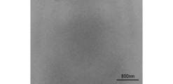
- crystal defect density of the ⁇ -Ga 2 O 3 based semiconductor film can be evaluated by a plane TEM observation (plan view), or cross-sectional TEM observation.
- plane TEM observation plane view
- cross-sectional TEM observation when the plane TEM observation of the surface of the semiconductor film is carried out, it can be carried out by using a general transmission electron microscope.
- TEM observation may be performed at an accelerating voltage of 300 kV.
- the test piece used for TEM observation is preferably one in which a sample is cut out so as to include one surface of the semiconductor film so that a measurement field of view of 50 ⁇ m ⁇ 50 ⁇ m can be observed.
- the crystal defect density can be evaluated from the planar TEM image of the surface of the test piece thus obtained.
- the semiconductor film of the present invention contains ⁇ -Ga 2 O 3 , Cr 2 O 3 , Fe 2 O 3 , Ti 2 O 3 , V 2 O 3 , Ir 2 O 3 , Rh 2 O 3 , and In 2 O 3. It can be composed of an ⁇ -Ga 2 O 3 system solid solution in which one or more components selected from the group consisting of Al 2 O 3 are solid-dissolved. All of these components have a corundum-type crystal structure and have relatively close lattice constants to each other. Therefore, the metal atoms of these components easily replace Ga atoms in the solid solution. Further, by dissolving these components in solid solution, it becomes possible to control the band gap, electrical characteristics, and / or lattice constant of the semiconductor film. The solid solution amount of these components can be appropriately changed according to the desired characteristics.
- the semiconductor film can contain a Group 14 element as a dopant at a ratio of 1.0 ⁇ 10 16 to 1.0 ⁇ 10 21 / cm 3 .
- the Group 14 element is the Group 14 element according to the periodic table formulated by the IUPAC (International Union of Pure and Applied Chemistry). Specifically, carbon (C), silicon (Si), and germanium (Ge). ), Tin (Sn) and lead (Pb).
- the amount of dopant can be appropriately changed according to the desired characteristics, but is preferably 1.0 ⁇ 10 16 to 1.0 ⁇ 10 21 / cm 3 , and more preferably 1.0 ⁇ 10 17 to 1.0. ⁇ 10 19 / cm 3 .
- these dopants are uniformly distributed in the film, and the concentrations of one front surface (front surface) and the opposite surface (back surface) are about the same. That is, it is preferable that the semiconductor film uniformly contains the Group 14 element as the dopant in the above ratio.
- the semiconductor film is an alignment film oriented in a specific plane orientation, for example, a c-axis alignment film.
- the orientation of the semiconductor film can be investigated by using a known method, but it can be investigated by performing reverse pole figure orientation mapping using, for example, an electron backscatter diffraction device (EBSD).
- EBSD electron backscatter diffraction device
- the thickness of the semiconductor film may be appropriately adjusted from the viewpoint of cost and required characteristics. That is, if it is too thick, it takes time to form a film, so it is preferable that the film is not extremely thick from the viewpoint of cost. Further, when a device that requires a particularly high dielectric strength is manufactured, a thick film is preferable. On the other hand, when manufacturing a device that requires conductivity in the vertical direction (thickness direction), a thin film is preferable. In this way, the film thickness may be appropriately adjusted according to the desired characteristics, but the thickness of the semiconductor film is typically 0.3 ⁇ m or more, more typically 0.3 to 50 ⁇ m, or 0.5. It is ⁇ 20 ⁇ m, or 0.5-10 ⁇ m.
- a thick film may be used, for example, 50 ⁇ m or more, or 100 ⁇ m or more, and there is no particular upper limit unless there is a cost limitation.
- the semiconductor film has an area of preferably 20 cm 2 or more, more preferably 70 cm 2 or more, and further preferably 170 cm 2 or more on one side thereof.
- the upper limit of the size of the semiconductor film is not particularly limited, but is typically 700 cm 2 or less on one side.
- the semiconductor film may be in the form of a self-supporting film of the film alone, or may be formed on a support substrate.
- a substrate having a corundum structure and oriented in two axes of the c-axis and the a-axis (biaxially oriented substrate) is preferable.
- a biaxially oriented substrate having a corundum structure as the support substrate, it is possible to serve as a seed crystal (base substrate for film formation) for heteroepitaxial growth of the semiconductor film.
- the biaxially oriented substrate may be a polycrystal, a mosaic crystal (a set of crystals whose crystal orientations are slightly deviated), or a single crystal.
- the main components of the support substrate are ⁇ -Al 2 O 3 , ⁇ -Cr 2 O 3 , ⁇ -Fe 2 O 3 , ⁇ -Ti 2 O 3 , ⁇ -V 2 O 3 , and ⁇ -Rh 2 O 3.
- a solid solution containing two or more kinds selected from the group consisting of 3 is preferable, and a solid solution of ⁇ -Cr 2 O 3 or ⁇ -Cr 2 O 3 and a dissimilar material is particularly preferable.
- corundum having sapphire, on corundum single crystal such as Cr 2 O 3 the a-axis length and / or c-axis length larger than the sapphire
- a composite base substrate having an orientation layer made of a material having a type crystal structure can also be used.
- the alignment layer is a material selected from the group consisting of ⁇ -Cr 2 O 3 , ⁇ -Fe 2 O 3 , ⁇ -Ti 2 O 3 , ⁇ -V 2 O 3 , and ⁇ -Rh 2 O 3.
- ⁇ -Al 2 O 3 , ⁇ -Cr 2 O 3 , ⁇ -Fe 2 O 3 , ⁇ -Ti 2 O 3 , ⁇ -V 2 O 3 , and ⁇ -Rh 2 O 3 selected from the group. It is preferable to contain a solid solution containing two or more of them.
- the semiconductor film formed on the film-forming substrate may be separated and reprinted on another support substrate.
- the material of the other support substrate is not particularly limited, but a suitable material may be selected from the viewpoint of material physical properties.
- a metal substrate such as Cu, a ceramic substrate such as SiC or AlN, or the like is preferable.
- a support substrate having such a coefficient of thermal expansion By using a support substrate having such a coefficient of thermal expansion, the difference in thermal expansion from the semiconductor film can be reduced, and as a result, cracks and peeling of the semiconductor film due to thermal stress can be suppressed.
- An example of such a support substrate is a substrate made of a Cu—Mo composite material.
- the composite ratio of Cu and Mo can be appropriately selected in consideration of the coefficient of thermal expansion matching with the semiconductor film, the thermal conductivity, the conductivity and the like.
- ⁇ -Cr 2 O 3 or a biaxially oriented substrate composed of a solid solution of ⁇ -Cr 2 O 3 and a dissimilar material, or ⁇ -Cr 2 O 3 or ⁇ -Cr 2 any of the composite substrate having O 3 and an alignment layer formed of a solid solution of different materials are preferred.
- the semiconductor film of the present invention has extremely few crystal defects and can exhibit high dielectric breakdown electric field characteristics.
- a technique for obtaining a semiconductor film having such a low crystal defect density has not been conventionally known.
- a substrate in which (Al x , Ga 1-x ) 2 O 3 layer (x 0.2 to 0.9) is introduced as a buffer layer between sapphire and ⁇ -Ga 2 O 3 layer.
- the formation of the ⁇ -Ga 2 O 3 layer using, the resulting ⁇ -Ga 2 O 3 layer, the density of the edge dislocation and screw dislocation respectively 3 ⁇ 10 8 / Cm 2 and 6 ⁇ 10 8 / cm 2 .
- Manufacturing method a semiconductor film of a semiconductor film, ⁇ -Ga 2 O 3, or ⁇ -Ga 2 O 3 based semiconductor film having the corundum crystalline structure composed of a solid solution, (104) in at least one surface side of the X
- the production method is not particularly limited as long as the film can be formed so that the half price width of the line locking curve is 500 arcsec or less.
- a biaxially oriented substrate composed of a solid solution of ⁇ -Cr 2 O 3 or ⁇ -Cr 2 O 3 and a dissimilar material, or ⁇ -Cr 2 O 3 or ⁇ -Cr 2 O It is preferable to use any of the composite base substrates having an orientation layer composed of a solid solution of 3 and a different material as the base substrate for film formation.
- a method for manufacturing a semiconductor film will be described in the order of (1) manufacturing of a composite substrate and (2) formation of a semiconductor film.
- a sapphire substrate is prepared, (b) a predetermined orientation precursor layer is prepared, and (c) the orientation precursor layer is heat-treated on the sapphire substrate. It can be preferably produced by converting at least a portion near the sapphire substrate into an alignment layer and, if desired, performing processing such as (d) grinding or polishing to expose the surface of the alignment layer.
- This alignment precursor layer becomes an alignment layer by heat treatment, and is a material having a corundum-type crystal structure whose a-axis length and / or c-axis length is larger than sapphire, or a-axis length and / or c-axis by heat treatment described later.
- the orientation precursor layer may contain trace components in addition to the material having a corundum-type crystal structure. According to such a manufacturing method, the growth of the alignment layer can be promoted by using the sapphire substrate as a seed crystal. That is, the high crystallinity and crystal orientation orientation peculiar to a single crystal of a sapphire substrate are inherited by the alignment layer.
- a sapphire substrate is prepared.
- the sapphire substrate used may have any orientation plane. That is, it may have a-plane, c-plane, r-plane, and m-plane, and may have a predetermined off-angle with respect to these planes.
- c-plane sapphire since it is c-axis oriented with respect to the surface, it is possible to easily heteroepitaxially grow an oriented layer oriented c-axis on it.
- a sapphire substrate to which a dopant has been added in order to adjust the electrical characteristics.
- dopants can be used as such dopants.
- orientation precursor layer A material having a corundum-type crystal structure whose a-axis length and / or c-axis length is larger than sapphire, or a corundum-type crystal structure whose a-axis length and / or c-axis length is larger than sapphire by heat treatment.
- An orientation precursor layer containing the material to be used is prepared.
- the method for forming the orientation precursor layer is not particularly limited, and a known method can be adopted.
- Examples of methods for forming an orientation precursor layer include AD (aerosol deposition) method, sol-gel method, hydrothermal method, sputtering method, thin-film deposition method, various CVD (chemical vapor deposition) methods, PLD method, and CVT (chemical vapor deposition) method. Methods such as the vapor phase transport method and the sublimation method can be mentioned.
- Examples of the CVD method include a thermal CVD method, a plasma CVD method, a mist CVD method, an MO (organic metal) CVD method, and the like.
- a method may be used in which a molded product of the orientation precursor is prepared in advance and the molded product is placed on a sapphire substrate.
- Such a molded product can be produced by molding the material of the orientation precursor by a method such as tape molding or press molding. Further, it is also possible to use a method in which a polycrystal prepared in advance by various CVD methods or sintering is used as the orientation precursor layer and placed on a sapphire substrate.
- a method of directly forming the orientation precursor layer by using an aerosol deposition (AD) method, various CVD methods, or a sputtering method is preferable.
- AD aerosol deposition
- various CVD methods various CVD methods
- a sputtering method it becomes possible to form a dense orientation precursor layer in a relatively short time, and it becomes easy to cause heteroepitaxial growth using a sapphire substrate as a seed crystal.
- the AD method does not require a high vacuum process and has a relatively high film formation rate, and is therefore preferable in terms of manufacturing cost.
- the sputtering method it is possible to form a film using a target made of the same material as the orientation precursor layer, but it is also possible to use a reactive sputtering method in which a metal target is used to form a film in an oxygen atmosphere. it can.
- a method of placing the molded product prepared in advance on sapphire is also preferable as a simple method, but since the orientation precursor layer is not dense, a process of densification is required in the heat treatment step described later.
- the method using a polycrystalline body prepared in advance as the orientation precursor layer requires two steps, a step of preparing the polycrystalline body and a step of heat treatment on the sapphire substrate.
- the AD method is a technology in which fine particles and fine particle raw materials are mixed with gas to form an aerosol, and this aerosol is jetted at high speed from a nozzle to collide with a substrate to form a film, which is said to be able to form a densified film at room temperature. It has characteristics.
- FIG. 1 shows an example of a film forming apparatus (aerosol deposition (AD) apparatus) used in such an AD method.
- the film forming apparatus 20 shown in FIG. 1 is configured as an apparatus used in the AD method of injecting raw material powder onto a substrate in an atmosphere of atmospheric pressure lower than atmospheric pressure.
- the film forming apparatus 20 includes an aerosol generation unit 22 that generates an aerosol of a raw material powder containing a raw material component, and a film forming unit 30 that injects the raw material powder onto a sapphire substrate 21 to form a film containing the raw material component.
- the aerosol generation unit 22 includes an aerosol generation chamber 23 that stores raw material powder and receives a carrier gas supply from a gas cylinder (not shown) to generate an aerosol, and a raw material supply pipe 24 that supplies the generated aerosol to the film forming unit 30.
- the aerosol generation chamber 23 and the aerosol in the aerosol are provided with a vibration exciter 25 that vibrates at a frequency of 10 to 100 Hz.
- the film-forming unit 30 has a film-forming chamber 32 that injects aerosols onto the sapphire substrate 21, a substrate holder 34 that is arranged inside the film-forming chamber 32 and fixes the sapphire substrate 21, and a substrate holder 34 on the X-axis-Y-axis. It is equipped with an XY stage 33 that moves in a direction. Further, the film forming section 30 includes an injection nozzle 36 having a slit 37 formed at the tip thereof to inject aerosol into the sapphire substrate 21, and a vacuum pump 38 for reducing the pressure in the film forming chamber 32.
- the AD method can control the film thickness, film quality, etc. depending on the film forming conditions.
- the form of the AD film is easily affected by the collision rate of the raw material powder with the substrate, the particle size of the raw material powder, the aggregated state of the raw material powder in the aerosol, the injection amount per unit time, and the like.
- the collision speed of the raw material powder with the substrate is affected by the differential pressure between the film forming chamber 32 and the injection nozzle 36, the opening area of the injection nozzle, and the like. If appropriate conditions are not used, the coating may become a powder or pores, so it is necessary to control these factors appropriately.
- the raw material powder of the orientation precursor can be molded to prepare the molded product.
- the orientation precursor layer is a press molded body.
- the press-molded product can be produced by press-molding the raw material powder of the orientation precursor based on a known method.
- the raw material powder is placed in a mold, preferably 100 to 400 kgf / cm 2 , more preferably 150. It may be produced by pressing at a pressure of about 300 kgf / cm 2 .
- the molding method is not particularly limited, and in addition to press molding, tape molding, casting molding, extrusion molding, a doctor blade method, and any combination thereof can be used.
- additives such as a binder, a plasticizer, a dispersant, and a dispersion medium are appropriately added to the raw material powder to form a slurry, and the slurry is passed through a narrow slit-shaped discharge port to form a sheet. It is preferable to discharge and mold.
- the thickness of the molded product formed into a sheet is not limited, but is preferably 5 to 500 ⁇ m from the viewpoint of handling. Further, when a thick orientation precursor layer is required, a large number of these sheet molded products may be stacked and used as a desired thickness.
- the portion near the sapphire substrate becomes an orientation layer by the subsequent heat treatment on the sapphire substrate.
- the molded product may contain trace components such as a sintering aid in addition to the material having or bringing about a corundum-type crystal structure.
- (C) Heat treatment of the alignment precursor layer on the sapphire substrate The sapphire substrate on which the alignment precursor layer is formed is heat-treated at a temperature of 1000 ° C. or higher. By this heat treatment, at least a portion of the alignment precursor layer near the sapphire substrate can be converted into a dense alignment layer. Further, this heat treatment makes it possible to grow the oriented layer heteroepitaxially. That is, by forming the alignment layer with a material having a corundum-type crystal structure, heteroepitaxial growth occurs in which the material having a corundum-type crystal structure grows as a seed crystal using a sapphire substrate during heat treatment. At that time, the crystals are rearranged, and the crystals are arranged according to the crystal plane of the sapphire substrate.
- the crystal axes of the sapphire substrate and the alignment layer can be aligned.
- the sapphire substrate and the alignment layer can both be oriented in the c-axis with respect to the surface of the base substrate.
- this heat treatment makes it possible to form a gradient composition region in a part of the alignment layer. That is, during the heat treatment, a reaction occurs at the interface between the sapphire substrate and the alignment precursor layer, and the Al component in the sapphire substrate diffuses into the alignment precursor layer and / or the component in the alignment precursor layer is in the sapphire substrate. Diffuses into a sapphire composition region composed of a solid solution containing ⁇ -Al 2 O 3 .
- the orientation precursor layer is in a non-oriented state at the time of its production, that is, it is an amorphous or non-oriented polycrystal, and it is preferable to cause crystal rearrangement using sapphire as a seed crystal during this heat treatment step. By doing so, the crystal defects reaching the surface of the alignment layer can be effectively reduced. The reason for this is not clear, but it is thought that the rearrangement of the crystal structure of the solid-phase orientation precursor layer once formed using sapphire as a seed may be effective in eliminating crystal defects.
- the heat treatment is not particularly limited as long as a corundum-type crystal structure is obtained and heteroepitaxial growth using a sapphire substrate as a seed occurs, and the heat treatment can be carried out in a known heat treatment furnace such as a tube furnace or a hot plate. Further, in addition to these heat treatments under normal pressure (pressless), pressure heat treatments such as hot press and HIP, and combinations of normal pressure heat treatments and pressure heat treatments can also be used.
- the heat treatment conditions can be appropriately selected depending on the material used for the alignment layer.
- the heat treatment atmosphere can be selected from atmospheric, vacuum, nitrogen and inert gas atmospheres.
- the preferred heat treatment temperature also varies depending on the material used for the alignment layer, but is preferably 1000 to 2000 ° C, more preferably 1200 to 2000 ° C, for example.
- the heat treatment temperature and holding time are related to the thickness of the alignment layer generated by heteroepitaxial growth and the thickness of the inclined composition region formed by diffusion with the sapphire substrate, and are related to the type of material, the target alignment layer, and the thickness of the inclined composition region. It can be adjusted as appropriate depending on the size. However, when a prefabricated molded product is used as an orientation precursor layer, it is necessary to sinter and densify it during heat treatment, and atmospheric firing at high temperature, hot pressing, HIP, or a combination thereof is preferable. ..
- the surface pressure is preferably 50 kgf / cm 2 or more, more preferably 100 kgf / cm 2 or more, particularly preferably 200 kgf / cm 2 or more, the upper limit is not particularly limited.
- the firing temperature is also not particularly limited as long as sintering, densification, and heteroepitaxial growth occur, but is preferably 1000 ° C. or higher, more preferably 1200 ° C. or higher, further preferably 1400 ° C. or higher, and particularly preferably 1600 ° C. or higher.
- the firing atmosphere can also be selected from atmosphere, vacuum, nitrogen and an inert gas atmosphere.
- the firing jig such as a mold, those made of graphite or alumina can be used.
- an oriented precursor layer or a surface layer having poor orientation or no orientation may exist or remain.
- the surface derived from the alignment precursor layer is subjected to processing such as grinding or polishing to expose the surface of the alignment layer.
- processing such as grinding or polishing to expose the surface of the alignment layer.
- a material having excellent orientation is exposed on the surface of the alignment layer, so that the semiconductor layer can be effectively epitaxially grown on the material.
- the method for removing the orientation precursor layer and the surface layer is not particularly limited, and examples thereof include a method for grinding and polishing and a method for ion beam milling. Polishing of the surface of the alignment layer is preferably performed by lapping using abrasive grains or chemical mechanical polishing (CMP).
- a semiconductor film is formed on the alignment layer of the obtained composite substrate.
- a semiconductor film forming method as long as a semiconductor film having the characteristics specified in the present invention is obtained, in other words, the half width of the X-ray locking curve of the (104) plane on at least one surface of the semiconductor film is 500 arcsec or less.
- a known method is possible. However, any one of mist CVD method, HVPE method, MBE method, MOCVD method, hydrothermal method and sputtering method is preferable, and mist CVD method, hydrothermal method or HVPE method is particularly preferable. Among these methods, the HVPE method will be described below.
- the HVPE method (halide vapor deposition method) is a type of CVD and is a method applicable to film formation of compound semiconductors such as Ga 2 O 3 and GaN.
- the Ga raw material and the halide are reacted to generate gallium halide gas, which is supplied onto the base substrate for film formation.
- O 2 gas is supplied onto the film-forming substrate, and the gallium halide gas reacts with the O 2 gas to grow Ga 2 O 3 on the film-forming substrate. It is a method that enables high-speed and thick film growth and has a wide range of achievements in industry, and examples of film formation of ⁇ -Ga 2 O 3 as well as ⁇ -Ga 2 O 3 have been reported.
- FIG. 2 shows an example of a vapor phase growth apparatus using the HVPE method.
- the vapor phase growth apparatus 40 using the HVPE method includes a reaction furnace 50, a susceptor 58 on which a film-forming substrate 56 is placed, an oxygen raw material supply source 51, a carrier gas supply source 52, and a Ga raw material supply source 53.
- a heater 54 and a gas discharge unit 57 are provided.
- An arbitrary reaction furnace that does not react with the raw material is applied to the reaction furnace 50, for example, a quartz tube. Any heater capable of heating up to at least 700 ° C. (preferably 900 ° C. or higher) is applied to the heater 54, for example, a resistance heating type heater.
- a metal Ga 55 is placed inside the Ga raw material supply source 53, and a halogen gas or a hydrogen halide gas, for example, HCl is supplied.
- the halogen gas or halogenated gas is preferably Cl 2 or HCl.
- the supplied halogen gas or halogenated gas reacts with the metal Ga55 to generate gallium halide gas, which is supplied to the film-forming base substrate 56.
- the gallium halide gas preferably contains GaCl and / or GaCl 3 .
- the oxygen raw material supply source 51 can supply an oxygen source selected from the group consisting of O 2 , H 2 O and N 2 O, but O 2 is preferable. These oxygen raw material gases are supplied to the film-forming substrate 56 at the same time as the gallium halide gas.
- the Ga raw material and the oxygen raw material gas may be supplied together with a carrier gas such as N 2 or a rare gas.
- the gas discharge unit 57 may be connected to a vacuum pump such as a diffusion pump or a rotary pump, for example, and controls not only the discharge of unreacted gas in the reaction furnace 50 but also the inside of the reaction furnace 50 under reduced pressure. You may. This can suppress the gas phase reaction and improve the growth rate distribution.
- a vacuum pump such as a diffusion pump or a rotary pump, for example, and controls not only the discharge of unreacted gas in the reaction furnace 50 but also the inside of the reaction furnace 50 under reduced pressure. You may. This can suppress the gas phase reaction and improve the growth rate distribution.
- ⁇ -Ga 2 O 3 is formed on the film-forming base substrate 56 by heating the film-forming base substrate 56 to a predetermined temperature using the heater 54 and simultaneously supplying the gallium halide gas and the oxygen raw material gas. Will be done.
- the film forming temperature is not particularly limited as long as ⁇ -Ga 2 O 3 is formed, but is typically 250 ° C to 900 ° C, for example.
- the partial pressure of the Ga raw material gas and the oxygen raw material gas is also not particularly limited.
- the partial pressure of the Ga raw material gas may be in the range of 0.05 kPa or more and 10 kPa or less
- the partial pressure of the oxygen raw material gas may be in the range of 0.25 kPa or more and 50 kPa or less.
- ⁇ -Ga 2 O 3 system semiconductor film containing a Group 14 element as a dopant or when forming a mixed crystal film with ⁇ -Ga 2 O 3 containing an oxide of In or Al. May supply these halides and the like by providing a separate supply source, or may mix and supply the halides from the Ga raw material supply source 53. Further, a material containing a Group 14 element, In, Al or the like may be placed in the same place as the metal Ga55, reacted with a halogen gas or a hydrogen halide gas, and supplied as a halide. Similar to gallium halide, those halide gases supplied to the base substrate 56 for film formation react with the oxygen raw material gas to form oxides, which are incorporated into the ⁇ -Ga 2 O 3 system semiconductor film.
- a single-layer structure film can be formed by keeping the supply amount of Ga raw material, oxygen raw material, etc. constant and appropriately controlling the film forming conditions. In this way, a semiconductor film having an extremely small X-ray locking curve full width at half maximum of 500 arcsec or less on the surface (104) can be formed on the composite substrate.
- the semiconductor film of the present invention has extremely small warpage after being formed on the film-forming substrate or when separated from the film-forming substrate to form a self-standing film.
- a biaxially oriented substrate composed of a solid solution of ⁇ -Cr 2 O 3 or ⁇ -Cr 2 O 3 and a different material, or ⁇ -Cr 2 O 3 or ⁇ -Cr.
- the amount of warpage can be particularly reduced.
- the amount of warpage when a 2-inch size semiconductor film is produced can be 30 ⁇ m or less, more preferably 20 ⁇ m or less, and further preferably 10 ⁇ m or less.
- the semiconductor film of the present invention can be a film having a small mosaic property.
- the ⁇ -Ga 2 O 3 film formed on the conventional sapphire substrate may be an aggregate (mosaic crystal) of domains having slightly different crystal orientations. The cause of this is not clear, but it can be mentioned that the film formation temperature is relatively low because ⁇ -Ga 2 O 3 is a metastable phase. Since the film formation temperature is low, it is difficult for the adsorbed components to migrate on the substrate surface, and step flow growth is difficult. For this reason, the growth mode of island-like growth (three-dimensional growth) tends to be dominant.
- the base substrate for film formation there may be a lattice mismatch between the semiconductor film and the sapphire, and the crystal orientation directions of the island-shaped growth portions (domains) may be slightly different from each other. For this reason, the domains do not meet completely and tend to form mosaic crystals.
- the semiconductor film of the present invention in particular as film formation base substrate, ⁇ -Cr 2 O 3, or ⁇ -Cr 2 O 3 and single crystal substrate composed of a solid solution of different materials, or ⁇ -Cr 2 O 3
- the film formation temperature is, for example, 600 ° C. or higher, preferably 700 ° C. or higher, more preferably 800 ° C. or higher, and further preferably 900 ° C. or higher.
- known methods such as XRC measurement, EBSD measurement, and TEM can be used, but the evaluation in the XRC half width as described above is particularly preferable.
- the obtained semiconductor film can be formed as it is or divided into semiconductor elements.
- the semiconductor film may be peeled off from the composite substrate to form a single film.
- a peeling layer may be provided in advance on the alignment layer surface (deposition surface) of the composite base substrate.
- Examples of such a release layer include those provided with a C injection layer and an H injection layer on the surface of the composite substrate. Further, C or H may be injected into the film at the initial stage of film formation of the semiconductor film to provide a release layer on the semiconductor film side.
- a support substrate (mounting substrate) different from the composite substrate is adhered and bonded to the surface of the semiconductor film formed on the composite substrate (that is, the surface opposite to the composite substrate), and then the semiconductor film is formed. It is also possible to peel off the composite substrate from the substrate.
- a support substrate (mounting substrate) a substrate having a coefficient of thermal expansion at 25 to 400 ° C. of 6 to 13 ppm / K, for example, a substrate made of a Cu—Mo composite material can be used.
- known methods such as brazing, soldering, and solid phase bonding can be mentioned.
- an electrode such as an ohmic electrode or a Schottky electrode, or another layer such as an adhesive layer may be provided between the semiconductor film and the support substrate.
- Example 1 A commercially available Cr 2 O 3 single crystal (size 8 mm ⁇ 8 mm, thickness 0.5 mm, c-plane, no off-angle) (hereinafter referred to as Cr 2 O 3 substrate) is used as the base substrate for film formation, and is as follows. Then, an ⁇ -Ga 2 O 3 film (semiconductor film) was formed.
- FIG. 3 schematically shows the mist CVD device 61 used in this example.
- the mist CVD apparatus 61 includes a dilution gas source 62a, a carrier gas source 62b, a flow rate control valve 63b, a mist generation source 64, a container 65, an ultrasonic vibrator 66, a quartz tube 67, a heater 68, a susceptor 70, and an exhaust port 71.
- a substrate 69 is placed on the susceptor 70.
- the flow rate control valve 63a is configured to be able to adjust the flow rate of the dilution gas sent out from the dilution gas source 62a, while the flow rate control valve 63b is configured to be able to adjust the flow rate of the carrier gas sent out from the carrier gas source 62b.
- the raw material solution 64a is contained in the mist generation source 64, while water 65a is contained in the container 65.
- the ultrasonic transducer 66 is attached to the bottom surface of the container 65.
- the quartz tube 67 forms a film forming chamber, and a heater 68 is installed in the peripheral portion of the quartz tube 67.
- the susceptor 70 is made of quartz, and the surface on which the substrate 69 is placed is inclined from the horizontal plane.
- the flow rate of the dilution gas was adjusted to 0.5 L / min and the flow rate of the carrier gas was adjusted to 1 L / min, respectively.
- Nitrogen gas was used as the dilution gas and the carrier gas.
- the ultrasonic transducer 66 was vibrated at 2.4 MHz, and the vibration was propagated to the raw material solution 64a through water 65a to mist the raw material solution 64a to generate mist 64b.
- This mist 64b is introduced into the quartz tube 67, which is a film forming chamber, by a diluent gas and a carrier gas, reacts in the quartz tube 67, and forms a film on the substrate 69 by a CVD reaction on the surface of the substrate 69. It was. In this way, a crystalline semiconductor film (semiconductor layer) was obtained.
- the film formation time was 60 minutes.
- EBSD Film surface on the film formation side composed of Ga oxide by SEM (Hitachi High-Technologies Corporation, SU-5000) equipped with an electron backscatter diffraction device (EBSD) (Nordlys Nano manufactured by Oxford Instruments). Inverse pole map orientation mapping was performed with a field of view of 500 ⁇ m ⁇ 500 ⁇ m. The conditions for this EBSD measurement were as follows.
- the Ga oxide film has a corundum-type crystal structure with c-axis orientation in the normal direction of the substrate and biaxial orientation with in-plane orientation. From these, it was shown that an alignment film made of ⁇ -Ga 2 O 3 was formed.
- a Ge (022) asymmetric reflection monochromator was used to convert CuK ⁇ rays into parallel monochromatic light.
- the full width at half maximum (FWHM) of the obtained (104) plane XRC profile shall be peak-searched after smoothing the profile using XRD analysis software (Made by Bruker-AXS, "LEPTOS” Ver4.03).
- XRD analysis software Mode by Bruker-AXS, "LEPTOS” Ver4.03
- Example 2 Formation of ⁇ -Ga 2 O 3 film in the same manner as in Example 1 except that the raw material solution in (1b) above was prepared as follows and the film formation time in (1d) above was set to 130 minutes. And various evaluations were performed. The results were as shown in Table 1.
- Example 3 The ⁇ -Ga 2 O 3 film was formed in the same manner as in Example 1 except that the temperature inside the quartz tube 67 was set to 460 ° C. in the above (1c) and the film formation time in the above (1d) was set to 200 minutes. Formation and various evaluations were performed. The results were as shown in Table 1.
- Example 4 In the above (1b'), tin (II) chloride dihydrate was added so that the atomic ratio of tin to gallium was 5.0 ⁇ 10-6, and in the above (1c), the temperature inside the quartz tube 67 was adjusted. The formation of the ⁇ -Ga 2 O 3 film and various evaluations were carried out in the same manner as in Example 2 except that the temperature was set to 460 ° C. and the film formation time was set to 110 minutes in (1d) above. The results were as shown in Table 1.
- Example 5 A composite substrate prepared as follows was used as the substrate for film formation, and tin (II) chloride dihydration was used so that the atomic ratio of tin to gallium was 0.7 in (1b') above.
- the formation of the ⁇ -Ga 2 O 3 film and various evaluations were carried out in the same manner as in Example 2 except that the substance was added and the film formation time was set to 280 minutes in the above (1d). The results were as shown in Table 1.
- the AD film formation conditions were as follows. That is, the carrier gas was N 2, and a ceramic nozzle having a slit having a long side of 5 mm and a short side of 0.3 mm was used.
- the scanning conditions of the nozzle are 0.5 mm / s, movement of 55 mm perpendicular to the long side of the slit and in the forward direction, movement of 5 mm in the direction of the long side of the slit, and vertical and return to the long side of the slit. Repeated scanning of moving 55 mm in the direction, moving 5 mm in the long side direction of the slit and in the direction opposite to the initial position, and when moving 55 mm from the initial position in the long side direction of the slit, scan in the opposite direction.
- the cycle of returning to the initial position was set as one cycle, and this was repeated for 500 cycles.
- the set pressure of the transport gas was adjusted to 0.06 MPa
- the flow rate was adjusted to 6 L / min
- the pressure in the chamber was adjusted to 100 Pa or less.
- the thickness of the AD film (alignment precursor layer) formed in this manner was about 100 ⁇ m.
- Cr, O and Al are detected in a range from the Cr oxide layer to a depth of 30 ⁇ m, and a Cr—Al oxide layer (gradient composition layer) having a thickness of about 30 ⁇ m is detected between the Cr oxide layer and the sapphire substrate.
- a Cr—Al oxide layer gradient composition layer
- the ratio of Cr and Al was different in the Cr—Al oxide layer, the Al concentration was high on the sapphire substrate side, and the Al concentration was low on the side close to the Cr oxide layer.
- the Cr oxide layer is a layer having a biaxially oriented corundum-type crystal structure oriented in the c-axis direction in the substrate normal direction and also in the in-plane direction. .. From these, it was shown that the front surface of the substrate was formed with an orientation layer made of ⁇ -Cr 2 O 3 . Based on the above results, the manufacturing process of the composite base substrate is schematically shown in FIGS. 5 (a) to 5 (d).
- (D3) XRD XRD in-plane measurement of the front surface of the substrate was performed using a multifunctional high-resolution X-ray diffraction (XRD) apparatus (D8 DISCOVER, manufactured by Bruker AXS Co., Ltd.). Specifically, after adjusting the Z-axis according to the height of the substrate surface, the (11-20) plane is adjusted with Chi, Phi, ⁇ , and 2 ⁇ to set the shaft under the following conditions. 2 ⁇ - ⁇ measurement was performed.
- XRD X-ray diffraction
- the a-axis length of the alignment layer was 4.961 ⁇ .
- Example 6 Except that tin (II) chloride dihydrate was added so that the atomic ratio of tin to gallium was 0.2 in (1b') above, and the film formation time was 600 minutes in (1d) above.
- the formation of the ⁇ -Ga 2 O 3 film and various evaluations were carried out in the same manner as in Example 5. The results were as shown in Table 1.
Landscapes
- Chemical & Material Sciences (AREA)
- Engineering & Computer Science (AREA)
- Materials Engineering (AREA)
- Organic Chemistry (AREA)
- Metallurgy (AREA)
- Power Engineering (AREA)
- Microelectronics & Electronic Packaging (AREA)
- Chemical Kinetics & Catalysis (AREA)
- General Chemical & Material Sciences (AREA)
- Crystallography & Structural Chemistry (AREA)
- Mechanical Engineering (AREA)
- Physics & Mathematics (AREA)
- Condensed Matter Physics & Semiconductors (AREA)
- General Physics & Mathematics (AREA)
- Ceramic Engineering (AREA)
- Computer Hardware Design (AREA)
- Inorganic Chemistry (AREA)
- Dispersion Chemistry (AREA)
- Crystals, And After-Treatments Of Crystals (AREA)
- Chemical Vapour Deposition (AREA)
- Liquid Deposition Of Substances Of Which Semiconductor Devices Are Composed (AREA)
- Physical Deposition Of Substances That Are Components Of Semiconductor Devices (AREA)
- Physical Vapour Deposition (AREA)
Abstract
結晶欠陥が著しく少ないα-Ga2O3系半導体膜が提供される。この半導体膜は、α-Ga2O3、又はα-Ga2O3系固溶体で構成されるコランダム型結晶構造を有し、半導体膜の少なくとも一方の表面における(104)面のX線ロッキングカーブ半値幅が500arcsec以下である。
Description
本発明は、半導体膜、特にα-Ga2O3系半導体膜に関する。
近年、酸化ガリウム(Ga2O3)が半導体用材料として着目されている。酸化ガリウムはα、β、γ、δ及びεの5つの結晶形を有することが知られているが、この中で、準安定相であるα-Ga2O3はバンドギャップが5.3eVと非常に大きく、パワー半導体用材料として期待を集めている。
例えば、特許文献1(特開2014-72533号公報)には、コランダム型結晶構造を有する下地基板と、コランダム型結晶構造を有する半導体層と、コランダム型結晶構造を有する絶縁膜とを備えた半導体装置が開示されており、サファイア基板上に、半導体層としてα-Ga2O3膜を成膜した例が記載されている。また、特許文献2(特開2016-25256号公報)には、コランダム構造を有する結晶性酸化物半導体を主成分として含むn型半導体層と、六方晶の結晶構造を有する無機化合物を主成分とするp型半導体層と、電極とを備えた半導体装置が開示されている。この特許文献2の実施例には、c面サファイア基板上に、n型半導体層として準安定相であるコランダム構造を有するα-Ga2O3膜を、p型半導体層として六方晶の結晶構造を有するα-Rh2O3膜を形成して、ダイオードを作製することが開示されている。
しかしながら、α-Ga2O3は準安定相であるため、単結晶基板が実用化されておらず、サファイア基板等へのヘテロエピタキシャル成長で形成されるのが一般的である。このような場合、サファイアとの格子定数差に起因して半導体膜中に応力が印加され、結晶欠陥が多数形成されたり、半導体膜に反りが生じたりする場合がある。
α-Ga2O3中の結晶欠陥低減に向けて、サファイアとα-Ga2O3層間にバッファ層を形成する手法が報告されている。例えば、非特許文献1(Applied Physics Express, vol.9, pages 071101-1~071101-4)には、サファイアとα-Ga2O3層間にバッファ層として(Alx,Ga1-x)2O3層(x=0.2~0.9)を導入することで、刃状転位とらせん転位が、それぞれ3×10⁸/cm2及び6×108/cm2となるとされる例が示されている。
Riena Jinno et al., Reduction in edge dislocation density in corundum-structured α-Ga2O3 layers on sapphire substrates with quasi-graded α-(Al,Ga)2O3 buffer layers, Applied Physics Express, Japan, The Japan Society of Applied Physics, June 1, 2016, vol.9, pages 071101-1 to 071101-4
しかしながら、α-Ga2O3膜を、高耐圧が要求されるパワー半導体等に利用する場合、結晶欠陥の多寡によって絶縁破壊電界特性が左右されるため、更なる結晶欠陥の低減が望まれる。
また、半導体膜の反りが大きいと、クラックが生じやすく、ハンドリング時に破断するおそれがある。すなわち、反りが大きい半導体膜上にミストCVDなどの成膜方法で機能層を形成する場合、膜厚や膜品質に分布が出るおそれがある。このため、反りが小さい半導体膜が望まれる。
さらに、α-Ga2O3膜は、チルト(成長方位の結晶軸の傾き)やツイスト(表面面内の結晶軸の回転)がわずかに異なる領域(ドメイン)が存在する、いわゆるモザイク結晶となる場合がある。これはα-Ga2O3層が準安定相であるため成膜温度が比較的低いことが原因の一つと考えられる。しかし、パワー半導体等に利用する場合、ドメイン間の粒界の存在によって絶縁破壊電界特性が低下するおそれがあるため、ドメイン形成の抑制も望まれる。
本発明者らは、今般、α-Ga2O3系半導体膜の少なくとも一方の表面における(104)面のX線ロッキングカーブ半値幅を500arcsec以下とすることで、結晶欠陥が著しく少ないα-Ga2O3系半導体膜を提供できるとの知見を得た。
したがって、本発明の目的は、結晶欠陥が著しく少ないα-Ga2O3系半導体膜を提供することにある。
本発明によれば、α-Ga2O3、又はα-Ga2O3系固溶体で構成されるコランダム型結晶構造を有する半導体膜であって、前記半導体膜の少なくとも一方の表面における(104)面のX線ロッキングカーブ半値幅が500arcsec以下である、半導体膜が提供される。
半導体膜
本発明の半導体膜は、α-Ga2O3、又はα-Ga2O3系固溶体で構成されるコランダム型結晶構造を有する。α-Ga2O3は、三方晶系の結晶群に属し、コランダム型結晶構造をとる。また、α-Ga2O3系固溶体は、α-Ga2O3に他の成分が固溶したものであり、コランダム型結晶構造が維持されている。
本発明の半導体膜は、α-Ga2O3、又はα-Ga2O3系固溶体で構成されるコランダム型結晶構造を有する。α-Ga2O3は、三方晶系の結晶群に属し、コランダム型結晶構造をとる。また、α-Ga2O3系固溶体は、α-Ga2O3に他の成分が固溶したものであり、コランダム型結晶構造が維持されている。
本発明のα-Ga2O3系半導体膜は、その少なくとも一方の表面における(104)面のX線ロッキングカーブ半値幅(以下、XRC半値幅という)が500arcsec以下であり、好ましくは150arcsec以下、より好ましくは100arcsec以下、さらに好ましくは50arcsec以下、特に好ましくは40arcsec以下である。すなわち、結晶欠陥やドメインを評価する手法として、(006)面や(104)面のX線ロッキングカーブ(XRC)測定を実施し、その半値幅で評価する方法が知られている。XRC測定では、真空チャック等で試料の反りを矯正して測定するのが一般的であるが、反り量が大きい場合は矯正困難な場合が多い。このため、X線ロッキングカーブ半値幅(以下、XRC半値幅という)は結晶欠陥やドメインに加え、反り量も反映するといえる。特に(104)面のXRC半値幅は、貫通刃状転位や貫通らせん転位等の各種欠陥、チルト(成長方位の結晶軸の傾き)やツイスト(表面面内の結晶軸の回転)が異なる領域(ドメイン)のモザイク性、及び反りの状態を全て反映するため、半導体膜の評価手法として好適である。したがって、上記範囲内のXRC範囲幅であると、結晶欠陥が少なく、モザイク性が小さく(ドメインが少なく)、反りも小さいことになり、その結果、このような半導体膜の表面上(又は内部)に機能層を形成する場合、機能層の内部に結晶欠陥が伝搬せず、高い絶縁破壊電界特性等の優れた特性を有する高品位な機能層が得られる。このように、半導体膜の表面における(104)面のXRC半値幅は小さいほど好ましく、測定に使用したX線源固有の半値幅と同等の値でも問題はないが、実際には30arcsec以上が好ましい。なお、本明細書において、少なくとも一方の表面とは、半導体膜の互いに対向する2つの主面(すなわち膜面ないし板面)の少なくともいずれか一方を意味し、おもて面及び裏面を問わない趣旨である。また、本明細書において、「表面」(ひょうめん)は物の外側をなす面を意味し、外部に露出しているか否かを問わないものとする(例えば、他の物に接触又は結合していてもよい)。一方、「おもて面」は「裏面」と対向する面を意味するものとする。
α-Ga2O3系半導体膜の表面における、(104)面のXRCプロファイルの測定は、一般的なXRD装置を用いて行うことができる。例えば、XRD装置としてBruker-AXS製D8-DISCOVERを用いる場合、2θ、ω、χ、及びφを調整してα-Ga2O3の(104)面のピークが出るように軸立てを行った後、管電圧40kV、管電流40mA、コリメータ径0.5mm、アンチスキャッタリングスリット3mmで、ω=15.5~19.5°の範囲、ωステップ幅0.005°、及び計数時間0.5秒の条件で測定を行えばよい。この測定は、Ge(022)非対称反射モノクロメーターでCuKα線を平行単色光化した上で行うのが好ましい。そして、(104)面のXRCプロファイルにおける半値幅は、XRD解析ソフトウェア(Bruker-AXS製、「LEPTOS」Ver4.03)を使用し、プロファイルのスムージングを行った後にピークサーチを行うことにより決定することができる。
また、本発明の半導体膜の少なくとも一方の表面における(006)面のXRC半値幅も小さい方が望ましく、好ましくは50arcsec以下、より好ましくは40arcsec以下である。(006)面のXRC半値幅は、測定に使用したX線源固有の半値幅と同等の値でも問題はないが、実際には30arcsec以上が好ましい。(006)面のXRC半値幅は、貫通らせん転位、チルト及び反りの情報を反映する。このため、上記範囲内のXRC半値幅であると、結晶欠陥が少なく、モザイク性が小さく(ドメインが少なく)、反りも小さいことになり、その結果、このような半導体膜の表面上(又は内部)に機能層を形成する場合、機能層の内部に結晶欠陥が伝搬せず、より一層高い絶縁破壊電界特性等の優れた特性を有する高品位な機能層が得られる。α-Ga2O3系半導体膜に対する、(006)面のXRCプロファイルの測定も、一般的なXRD装置を用いて行うことができる。例えば、XRD装置としてBruker-AXS製D8-DISCOVERを用いる場合の測定条件は、2θ、ω、χ、及びφを調整してα-Ga2O3の(006)面のピークが出るように軸立てを行った後、ω=18.0~22.0°とすること以外は(104)面に関して前述した条件と同様であることができる。
本発明のα-Ga2O3系半導体膜において、半導体膜の一方の表面(以下、おもて面という)における(104)面のXRC半値幅(FWHM-T)に対する、半導体膜のおもて面に対向する表面(以下、裏面という)における(104)面のXRC半値幅(FWHM-B)の比であるFWHM-B/FWHM-Tは、FWHM-B/FWHM-T>1の関係にあることが好ましい。例えば、成膜用下地基板上に半導体膜を形成し、成膜側の表面とそれに対向する側の表面(成膜用下地基板と隣接する表面)のXRC半値幅を測定したとき、成膜側の表面のXRC半値幅の方が成膜用下地基板と隣接する表面のXRC半値幅より小さくなる場合がある。このとき、成膜側表面(おもて面)のXRC半値幅をFWHM-T、成膜用下地基板と隣接する表面(裏面)のXRC半値幅をFWHM-Bとすると、FWHM-B/FWHM-T>1となる。前述したとおり、XRC半値幅は各種欠陥やモザイク性を反映するため、上記関係は裏面よりも表面の方が品質が改善したことを示す。言い換えると、半導体膜の成膜中に結晶欠陥やモザイク性が低減したことを意味する。このような膜において、XRC半値幅が小さい表面上(又は内部)に機能層を形成することで、高品質な機能層等を形成することができる。具体的には、FWHM-B/FWHM-Tは、1.0を超えるのが好ましく、より好ましくは1.2以上、さらに好ましくは1.3以上、特に好ましくは1.7以上である。FWHM-B/FWHM-Tの上限は特に限定されないが、例えば5.0以下である。ここで、前述したとおり、半導体膜の裏面は、XRC半値幅が小さい側の表面(おもて面)に対向する側の表面を指すが、典型的には、半導体膜の成膜に用いた下地基板と隣接している(又は隣接していた)側の面を指す。
なお、α-Ga2O3系半導体膜の成膜用下地基板と隣接する表面(すなわち裏面)における(104)面のXRCプロファイルの測定は、自立した半導体膜の場合は成膜側の表面(おもて面)と同様の方法で実施することができる。半導体膜が成膜用下地基板等の支持基板(以下、第1の支持基板という)上に形成されている場合は、第1の支持基板上の半導体膜の表面(すなわち第1の支持基板とは反対側の面)に異なる支持基板(以下、第2の支持基板という)を接着及び接合し、その後、半導体膜から第1の支持基板を剥離又は研削及び研磨にて除去して半導体膜裏面を露出させた後に測定することが可能である。第2の支持基板や接合及び接着方法は、半導体膜に反りを生じることなく半導体膜を支持できれば特に限定されない。例えば、第2の支持基板としてサファイア等の単結晶基板や、Cu-Mo複合材料等の熱膨張特性が半導体膜と近い材料で構成された基板を用いることができる。また、半導体膜と第2の支持基板の接着方法としては、ロウ付け、半田、固相接合、エポキシ等の接着剤を用いることができる。第1の支持基板の除去方法は、半導体膜の品質に影響しない限り特に限定されない。例えば、研削及び研磨により第1の支持基板を除去する場合、半導体膜に加工による変質層が導入され、XRCプロファイルに影響する恐れがある。このため、支持基板を除去した後、CMPやイオンミリングによって半導体膜に導入された加工変質層を除去することが望ましい。また、半導体膜のXRCプロファイルが得ることができる限り、第1の支持基板を全て除去する必要はない。すなわち、第1の支持基板を薄くすることで(例えば厚さ1μm程度)、第1の支持基板をX線が透過して半導体膜のXRCプロファイルを得ることができる。
本発明のα-Ga2O3系半導体膜は、その少なくとも一方の表面の結晶欠陥密度が1.0×10⁶/cm2以下であることが好ましく、より好ましくは1.0×105/cm2以下、さらに好ましくは4.0×103/cm2以下、特に好ましくは1.0×103/cm2以下である。このように結晶欠陥密度が著しく低い半導体膜は、絶縁破壊電界特性に優れ、パワー半導体の用途に適している。また、このような表面上(又は内部)に機能層を形成する場合、高い絶縁破壊電界特性等の優れた特性を有する高品位な機能層が得られる。結晶欠陥密度の下限は特に限定がなく、低い方が好ましい。なお、本明細書において、結晶欠陥とは、貫通刃状転位、貫通らせん転位、貫通混合転位、及び基底面転位を指し、結晶欠陥密度は、各転位密度の合計のことである。なお、基底面転位は、半導体膜にオフ角がある場合に問題となるものであり、オフ角がない場合は半導体膜の表面まで露出しないため、問題とならない。例えば、貫通刃状転位を3×104/cm2、貫通らせん転位を6×104/cm2、貫通混合転位を4×104/cm2含むとすれば、結晶欠陥密度は1.3×105/cm2となる。
α-Ga2O3系半導体膜の結晶欠陥密度は、平面TEM観察(プランビュー)、又は断面TEM観察により評価することができる。例えば、半導体膜表面の平面TEM観察を実施する場合、一般的な透過型電子顕微鏡を用いて行うことができる。例えば、透過型電子顕微鏡として日立製H-90001UHR-Iを用いる場合、加速電圧300kVでTEM観察を行えばよい。TEM観察に用いる試験片は、半導体膜の一方の表面が含まれるようにサンプルを切り出し、測定視野50μm×50μmの範囲が観察できるようなものが好ましい。より具体的には、測定視野4.1μm×3.1μmの領域が8箇所以上観察可能で、測定視野周辺の厚さが150nmとなるようにイオンミリングによって加工すればよい。こうして得られた試験片表面の平面TEM像から結晶欠陥密度を評価することができる。
本発明の半導体膜は、α-Ga2O3に、Cr2O3、Fe2O3、Ti2O3、V2O3、Ir2O3、Rh2O3、In2O3及びAl2O3からなる群から選択される1種以上の成分が固溶したα-Ga2O3系固溶体で構成されるものとすることができる。これらの成分はいずれもコランダム型結晶構造を有し、かつ、互いに格子定数が比較的近い。したがって、これらの成分の金属原子は固溶体中で容易にGa原子を置換する。また、これらの成分を固溶させることで半導体膜のバンドギャップ、電気特性、及び/又は格子定数を制御することが可能となる。これらの成分の固溶量は所望の特性に合わせて適宜変更することができる。
半導体膜は、ドーパントとして14族元素を1.0×10¹⁶~1.0×10²¹/cm3の割合で含むことができる。ここで、14族元素はIUPAC(国際純正・応用化学連合)が策定した周期律表による第14族元素のことであり、具体的には、炭素(C)、珪素(Si)、ゲルマニウム(Ge)、錫(Sn)及び鉛(Pb)のいずれかの元素である。ドーパント量は所望の特性に合わせて適宜変更することができるが、好ましくは、1.0×1016~1.0×1021/cm3、より好ましくは1.0×1017~1.0×1019/cm3である。これらのドーパントは膜中に均一に分布し、一方の表面(おもて面)とそれに対向する側の表面(裏面)の濃度は同程度であることが好ましい。すなわち、半導体膜はドーパントとして14族元素を上記割合で均一に含むのが好ましい。
さらに、半導体膜が特定の面方位に配向した配向膜であるのが好ましく、例えばc軸配向膜である。半導体膜の配向性は公知の手法を用いて調べることができるが、例えば、電子線後方散乱回折装置(EBSD)を用いて、逆極点図方位マッピングを行うことで、調べることができる。
半導体膜の厚さは、コスト面及び要求される特性の観点から適宜調整すればよい。すなわち、厚すぎると成膜に時間がかかるため、コスト面からは極端に厚くない方が好ましい。また、特に高い絶縁耐圧が要求されるデバイスを作製する場合には、厚い膜とすることが好ましい。一方、縦方向(厚さ方向)の導電性が要求されるデバイスを作製する場合には、薄い膜とすることが好ましい。このように所望の特性に合わせて膜厚を適宜調整すればよいが、半導体膜の厚さは、典型的には0.3μm以上、より典型的には0.3~50μm、又は0.5~20μm、又は0.5~10μmである。このような範囲の厚さとすることで、コスト面と半導体特性の両立が可能となる。また、自立した半導体膜が必要な場合は厚い膜とすればよく、例えば50μm以上、又は100μm以上であり、コスト面の制限がない限り特に上限はない。
半導体膜は、その片面が、好ましくは20cm2以上、より好ましくは70cm2以上、さらに好ましくは170cm2以上の面積を有する。このように半導体膜を大面積化することにより、一枚の半導体膜から半導体素子を多数個取りすることが可能となり、製造コストの低減化を図ることができる。半導体膜の大きさの上限は特に限定されるものではないが、典型的には、片面700cm2以下である。
半導体膜は、膜単独の自立膜の形態であってもよいし、支持基板上に形成されたものであってもよい。支持基板として、コランダム構造を有し、c軸及びa軸の二軸に配向した基板(二軸配向基板)が好ましい。支持基板にコランダム構造を有する二軸配向基板を用いることで、半導体膜がヘテロエピタキシャル成長するための種結晶(成膜用下地基板)を兼ねることが可能となる。二軸配向基板は、多結晶やモザイク結晶(結晶方位が若干ずれた結晶の集合)であってもよいし、単結晶であってもよい。コランダム構造を有する限り、単一の材料で構成されるものでもよいし、複数の材料の固溶体であってもよい。支持基板の主成分は、α-Al2O3、α-Cr2O3、α-Fe2O3、α-Ti2O3、α-V2O3、及びα-Rh2O3からなる群から選択される材料、又はα-Al2O3、α-Cr2O3、α-Fe2O3、α-Ti2O3、α-V2O3、及びα-Rh2O3からなる群から選択される2種以上を含む固溶体が好ましく、α-Cr2O3、又はα-Cr2O3と異種材料との固溶体が特に好ましい。
また、支持基板兼ヘテロエピタキシャル成長用の種結晶(成膜用下地基板)として、サファイア、Cr2O3等のコランダム単結晶上に、サファイアよりも大きいa軸長及び/又はc軸長を有するコランダム型結晶構造を有する材料で構成された配向層を形成した複合下地基板も用いることができる。この場合、配向層は、α-Cr2O3、α-Fe2O3、α-Ti2O3、α-V2O3、及びα-Rh2O3からなる群から選択される材料、又はα-Al2O3、α-Cr2O3、α-Fe2O3、α-Ti2O3、α-V2O3、及びα-Rh2O3からなる群から選択される2種以上を含む固溶体を含むのが好ましい。
また、成膜用下地基板上に作製した半導体膜を分離し、別の支持基板に転載してもよい。別の支持基板の材質は特に限定はないが、材料物性の観点から好適なものを選択すればよい。例えば、熱伝導率の観点では、Cu等の金属基板、SiC、AlN等のセラミックス基板等が好ましい。また、25~400℃での熱膨張率が6~13ppm/Kである基板を用いるのも好ましい。すなわち、半導体膜は25~400℃での熱膨張率が6~13ppm/Kである支持基板上に設けられるのも好ましく、そのような半導体膜ないし複合材料も本発明の好ましい態様として提供される。このような熱膨張率を有する支持基板を用いることで、半導体膜との熱膨張差を小さくすることができ、その結果、熱応力による半導体膜中のクラック発生や膜剥がれ等を抑制できる。このような支持基板の例としては、Cu-Mo複合材料で構成される基板が挙げられる。CuとMoの複合比率は、半導体膜との熱膨張率マッチング、熱伝導率、導電率等を勘案して、適宜選択することができる。
半導体膜の支持基板としては、α-Cr2O3、若しくはα-Cr2O3と異種材料との固溶体で構成される二軸配向基板、又はα-Cr2O3、若しくはα-Cr2O3と異種材料との固溶体で構成される配向層を有する複合基板のいずれかが好ましい。こうすることで、半導体膜がヘテロエピタキシャル成長するための種結晶(成膜用下地基板)と支持基板を兼ねることができる上、半導体膜中の結晶欠陥を著しく低減することができる。
前述のとおり、本発明の半導体膜は、結晶欠陥が著しく少なく、高い絶縁破壊電界特性を呈することが可能である。本発明者の知る限り、このように結晶欠陥密度が低い半導体膜を得る技術は従来知られていない。例えば、非特許文献1には、サファイアとα-Ga2O3層間にバッファ層として(Alx,Ga1-x)2O3層(x=0.2~0.9)を導入した基板を用いてα-Ga2O3層を成膜することが開示されているが、得られたα-Ga2O3層は、その刃状転位とらせん転位の密度が、それぞれ3×10⁸/cm2及び6×108/cm2である。
半導体膜の製造方法
半導体膜は、α-Ga2O3、又はα-Ga2O3系固溶体で構成されるコランダム型結晶構造を有する半導体膜を、少なくとも一方の表面における(104)面のX線ロッキングカーブ半値幅が500arcsec以下となるように成膜できる限り、その製法は特に限定されるものではない。しかしながら、前述したような、α-Cr2O3、若しくはα-Cr2O3と異種材料との固溶体で構成される二軸配向基板、又はα-Cr2O3、若しくはα-Cr2O3と異種材料との固溶体で構成される配向層を有する複合下地基板のいずれかを成膜用下地基板として使用することが好ましい。以下に、半導体膜の製造方法を、(1)複合下地基板の作製、(2)半導体膜の形成の順に説明する。
半導体膜は、α-Ga2O3、又はα-Ga2O3系固溶体で構成されるコランダム型結晶構造を有する半導体膜を、少なくとも一方の表面における(104)面のX線ロッキングカーブ半値幅が500arcsec以下となるように成膜できる限り、その製法は特に限定されるものではない。しかしながら、前述したような、α-Cr2O3、若しくはα-Cr2O3と異種材料との固溶体で構成される二軸配向基板、又はα-Cr2O3、若しくはα-Cr2O3と異種材料との固溶体で構成される配向層を有する複合下地基板のいずれかを成膜用下地基板として使用することが好ましい。以下に、半導体膜の製造方法を、(1)複合下地基板の作製、(2)半導体膜の形成の順に説明する。
(1)複合下地基板の作製
複合下地基板は、(a)サファイア基板を準備し、(b)所定の配向前駆体層を作製し、(c)サファイア基板上で配向前駆体層を熱処理してその少なくともサファイア基板近くの部分を配向層に変換し、所望により(d)研削や研磨等の加工を施して配向層の表面を露出させることにより好ましく製造することができる。この配向前駆体層は熱処理により配向層となるものであり、a軸長及び/又はc軸長がサファイアより大きいコランダム型結晶構造を有する材料、あるいは後述する熱処理によってa軸長及び/又はc軸長がサファイアより大きいコランダム型結晶構造となる材料を含む。また、配向前駆体層はコランダム型結晶構造を有する材料の他に、微量成分を含んでいてもよい。このような製造方法によれば、サファイア基板を種結晶として配向層の成長を促すことができる。すなわち、サファイア基板の単結晶特有の高い結晶性と結晶配向方位が配向層に引き継がれる。
複合下地基板は、(a)サファイア基板を準備し、(b)所定の配向前駆体層を作製し、(c)サファイア基板上で配向前駆体層を熱処理してその少なくともサファイア基板近くの部分を配向層に変換し、所望により(d)研削や研磨等の加工を施して配向層の表面を露出させることにより好ましく製造することができる。この配向前駆体層は熱処理により配向層となるものであり、a軸長及び/又はc軸長がサファイアより大きいコランダム型結晶構造を有する材料、あるいは後述する熱処理によってa軸長及び/又はc軸長がサファイアより大きいコランダム型結晶構造となる材料を含む。また、配向前駆体層はコランダム型結晶構造を有する材料の他に、微量成分を含んでいてもよい。このような製造方法によれば、サファイア基板を種結晶として配向層の成長を促すことができる。すなわち、サファイア基板の単結晶特有の高い結晶性と結晶配向方位が配向層に引き継がれる。
(a)サファイア基板の準備
複合下地基板を作製するには、まず、サファイア基板を準備する。用いるサファイア基板は、いずれの方位面を有するものであってもよい。すなわち、a面、c面、r面、m面を有するものであってもよく、これらの面に対して所定のオフ角を有するものであってもよい。例えばc面サファイアを用いた場合、表面に対してc軸配向しているため、その上に、容易にc軸配向させた配向層をヘテロエピタキシャル成長させることが可能となる。また、電気特性を調整するために、ドーパントを加えたサファイア基板を用いることも可能である。このようなドーパントとしては公知のものが使用可能である。
複合下地基板を作製するには、まず、サファイア基板を準備する。用いるサファイア基板は、いずれの方位面を有するものであってもよい。すなわち、a面、c面、r面、m面を有するものであってもよく、これらの面に対して所定のオフ角を有するものであってもよい。例えばc面サファイアを用いた場合、表面に対してc軸配向しているため、その上に、容易にc軸配向させた配向層をヘテロエピタキシャル成長させることが可能となる。また、電気特性を調整するために、ドーパントを加えたサファイア基板を用いることも可能である。このようなドーパントとしては公知のものが使用可能である。
(b)配向前駆体層の作製
a軸長及び/又はc軸長がサファイアより大きいコランダム型結晶構造を有する材料、又は熱処理によってa軸長及び/又はc軸長がサファイアより大きいコランダム型結晶構造となる材料を含む配向前駆体層を作製する。配向前駆体層を形成する方法は特に限定されず、公知の手法が採用可能である。配向前駆体層を形成する方法の例としては、AD(エアロゾルデポジション)法、ゾルゲル法、水熱法、スパッタリング法、蒸着法、各種CVD(化学気相成長)法、PLD法、CVT(化学気相輸送)法、昇華法等の手法等が挙げられる。CVD法の例としては、熱CVD法、プラズマCVD法、ミストCVD法、MO(有機金属)CVD法等が挙げられる。あるいは、配向前駆体の成形体を予め作製し、この成形体をサファイア基板上に載置する手法であってもよい。このような成形体は、配向前駆体の材料を、テープ成形又はプレス成形等の手法で成形することで作製可能である。また、配向前駆体層として予め各種CVD法や焼結等で作製した多結晶体を使用し、サファイア基板上に載置する方法も用いることができる。
a軸長及び/又はc軸長がサファイアより大きいコランダム型結晶構造を有する材料、又は熱処理によってa軸長及び/又はc軸長がサファイアより大きいコランダム型結晶構造となる材料を含む配向前駆体層を作製する。配向前駆体層を形成する方法は特に限定されず、公知の手法が採用可能である。配向前駆体層を形成する方法の例としては、AD(エアロゾルデポジション)法、ゾルゲル法、水熱法、スパッタリング法、蒸着法、各種CVD(化学気相成長)法、PLD法、CVT(化学気相輸送)法、昇華法等の手法等が挙げられる。CVD法の例としては、熱CVD法、プラズマCVD法、ミストCVD法、MO(有機金属)CVD法等が挙げられる。あるいは、配向前駆体の成形体を予め作製し、この成形体をサファイア基板上に載置する手法であってもよい。このような成形体は、配向前駆体の材料を、テープ成形又はプレス成形等の手法で成形することで作製可能である。また、配向前駆体層として予め各種CVD法や焼結等で作製した多結晶体を使用し、サファイア基板上に載置する方法も用いることができる。
しかしながら、エアロゾルデポジション(AD)法、各種CVD法、又はスパッタリング法を用いて配向前駆体層を直接形成する手法が好ましい。これらの方法を用いることで緻密な配向前駆体層を比較的短時間で形成することが可能となり、サファイア基板を種結晶としたヘテロエピタキシャル成長を生じさせることが容易になる。特に、AD法は高真空のプロセスを必要とせず、成膜速度も相対的に速いため、製造コストの面でも好ましい。スパッタリング法を用いる場合は、配向前駆体層と同材料のターゲットを用いて成膜することも可能であるが、金属ターゲットを使用し、酸素雰囲気下で成膜する反応性スパッタ法も用いることができる。予め作製した成形体をサファイア上に載置する手法も簡易な手法として好ましいが、配向前駆体層が緻密ではないため、後述する熱処理工程において緻密化するプロセスを必要とする。配向前駆体層として予め作製した多結晶体を用いる手法では、多結晶体を作製する工程と、サファイア基板上で熱処理する工程の二つが必要となる。また、多結晶体とサファイア基板の密着性を高めるため、多結晶体の表面を十分に平滑にしておく等の工夫も必要である。いずれの手法も公知の条件を用いることができるが、AD法を用いて配向前駆体層を直接形成する手法と、予め作製した成形体をサファイア基板上に載置する手法について、以下に説明する。
AD法は、微粒子や微粒子原料をガスと混合してエアロゾル化し、このエアロゾルをノズルから高速噴射して基板に衝突させ、被膜を形成する技術であり、常温で緻密化された被膜を形成できるという特徴を有している。このようなAD法で用いられる成膜装置(エアロゾルデポジション(AD)装置)の一例を図1に示す。図1に示される成膜装置20は、大気圧より低い気圧の雰囲気下で原料粉末を基板上に噴射するAD法に用いられる装置として構成されている。この成膜装置20は、原料成分を含む原料粉末のエアロゾルを生成するエアロゾル生成部22と、原料粉末をサファイア基板21に噴射して原料成分を含む膜を形成する成膜部30とを備えている。エアロゾル生成部22は、原料粉末を収容し図示しないガスボンベからのキャリアガスの供給を受けてエアロゾルを生成するエアロゾル生成室23と、生成したエアロゾルを成膜部30へ供給する原料供給管24と、エアロゾル生成室23及びその中のエアロゾルに10~100Hzの振動数で振動が付与する加振器25とを備えている。成膜部30は、サファイア基板21にエアロゾルを噴射する成膜チャンバ32と、成膜チャンバ32の内部に配設されサファイア基板21を固定する基板ホルダ34と、基板ホルダ34をX軸-Y軸方向に移動するX-Yステージ33とを備えている。また、成膜部30は、先端にスリット37が形成されエアロゾルをサファイア基板21へ噴射する噴射ノズル36と、成膜チャンバ32を減圧する真空ポンプ38とを備えている。
AD法は、成膜条件によって膜厚や膜質等を制御できることが知られている。例えば、AD膜の形態は、原料粉末の基板への衝突速度、原料粉末の粒径、エアロゾル中の原料粉末の凝集状態、単位時間当たりの噴射量等に影響を受けやすい。原料粉末の基板への衝突速度は、成膜チャンバ32と噴射ノズル36内の差圧や、噴射ノズルの開口面積等に影響を受ける。適切な条件を用いない場合、被膜が圧粉体となったり気孔を生じたりする場合があるので、これらのファクターを適切に制御することが必要である。
配向前駆体層を予め作製した成形体を用いる場合、配向前駆体の原料粉末を成形して成形体を作製することができる。例えば、プレス成形を用いる場合、配向前駆体層はプレス成形体である。プレス成形体は、配向前駆体の原料粉末を公知の手法に基づきプレス成形することで作製可能であり、例えば、原料粉末を金型に入れ、好ましくは100~400kgf/cm2、より好ましくは150~300kgf/cm2の圧力でプレスすることにより作製すればよい。また、成形方法は特に限定されず、プレス成形の他、テープ成形、鋳込み成形、押出し成形、ドクターブレード法、及びこれらの任意の組合せを用いることができる。例えば、テープ成形を用いる場合、原料粉末にバインダー、可塑剤、分散剤、分散媒等の添加物を適宜加えてスラリー化し、このスラリーをスリット状の細い吐出口を通過させることにより、シート状に吐出及び成形するのが好ましい。シート状に成形した成形体の厚さに限定はないが、ハンドリングの観点では5~500μmであるのが好ましい。また、厚い配向前駆体層が必要な場合はこのシート成形体を多数枚積み重ねて、所望の厚さとして使用すればよい。
これらの成形体はその後のサファイア基板上での熱処理によりサファイア基板近くの部分が配向層となるものである。上述したように、このような手法では後述する熱処理工程において成形体を焼結させ、緻密化する必要がある。このため、成形体はコランダム型結晶構造を有する又はもたらす材料の他に、焼結助剤等の微量成分を含んでいてもよい。
(c)サファイア基板上の配向前駆体層の熱処理
配向前駆体層が形成されたサファイア基板を1000℃以上の温度で熱処理する。この熱処理により、配向前駆体層の少なくともサファイア基板近くの部分を緻密な配向層に変換することが可能となる。また、この熱処理により、配向層をヘテロエピタキシャル成長させることが可能となる。すなわち、配向層をコランダム型結晶構造を有する材料で構成することで、熱処理時にコランダム型結晶構造を有する材料がサファイア基板を種結晶として結晶成長するヘテロエピタキシャル成長が生じる。その際、結晶の再配列が起こり、サファイア基板の結晶面に倣って結晶が配列する。この結果、サファイア基板と配向層の結晶軸を揃えることができる。例えば、c面サファイア基板を用いると、サファイア基板と配向層が下地基板の表面に対していずれもc軸配向した態様とすることが可能となる。その上、この熱処理により、配向層の一部に傾斜組成領域を形成することが可能となる。すなわち、熱処理の際に、サファイア基板と配向前駆体層の界面で反応が生じ、サファイア基板中のAl成分が配向前駆体層中に拡散する及び/又は配向前駆体層中の成分がサファイア基板中に拡散して、α-Al2O3を含む固溶体で構成される傾斜組成領域が形成される。
配向前駆体層が形成されたサファイア基板を1000℃以上の温度で熱処理する。この熱処理により、配向前駆体層の少なくともサファイア基板近くの部分を緻密な配向層に変換することが可能となる。また、この熱処理により、配向層をヘテロエピタキシャル成長させることが可能となる。すなわち、配向層をコランダム型結晶構造を有する材料で構成することで、熱処理時にコランダム型結晶構造を有する材料がサファイア基板を種結晶として結晶成長するヘテロエピタキシャル成長が生じる。その際、結晶の再配列が起こり、サファイア基板の結晶面に倣って結晶が配列する。この結果、サファイア基板と配向層の結晶軸を揃えることができる。例えば、c面サファイア基板を用いると、サファイア基板と配向層が下地基板の表面に対していずれもc軸配向した態様とすることが可能となる。その上、この熱処理により、配向層の一部に傾斜組成領域を形成することが可能となる。すなわち、熱処理の際に、サファイア基板と配向前駆体層の界面で反応が生じ、サファイア基板中のAl成分が配向前駆体層中に拡散する及び/又は配向前駆体層中の成分がサファイア基板中に拡散して、α-Al2O3を含む固溶体で構成される傾斜組成領域が形成される。
なお、各種CVD法やスパッタリング法、PLD法、CVT法、昇華法等の方法では、1000℃以上の熱処理を経ることなくサファイア基板上にヘテロエピタキシャル成長を生じる場合があることが知られている。しかし、配向前駆体層はその作製時には配向していない状態、すなわち非晶質や無配向の多結晶であり、本熱処理工程時にサファイアを種結晶として結晶の再配列を生じさせることが好ましい。こうすることで、配向層表面に到達する結晶欠陥を効果的に低減することができる。この理由は定かではないが、一旦成膜された固相の配向前駆体層がサファイアを種として結晶構造の再配列を生じることが結晶欠陥の消滅に効果があるのではないかと考えている。
熱処理は、コランダム型結晶構造が得られ、サファイア基板を種としたヘテロエピタキシャル成長が生じるかぎり特に限定されず、管状炉やホットプレート等、公知の熱処理炉で実施することができる。また、これらの常圧(プレスレス)での熱処理だけでなく、ホットプレスやHIP等の加圧熱処理や、常圧熱処理と加圧熱処理の組み合わせも用いることができる。熱処理条件は、配向層に用いる材料によって適宜選択できる。例えば、熱処理の雰囲気は大気、真空、窒素及び不活性ガス雰囲気から選択することができる。好ましい熱処理温度も配向層に用いる材料によって変わるが、例えば1000~2000℃が好ましく、1200~2000℃がさらに好ましい。熱処理温度や保持時間はヘテロエピタキシャル成長で生じる配向層の厚さやサファイア基板との拡散で形成される傾斜組成領域の厚さと関係しており、材料の種類、狙いとする配向層、傾斜組成領域の厚さ等によって適宜調整することができる。ただし、予め作製した成形体を配向前駆体層として用いる場合、熱処理中に焼結して緻密化させる必要があり、高温での常圧焼成、ホットプレス、HIP、又はそれらの組み合わせが好適である。例えば、ホットプレスを用いる場合、面圧は50kgf/cm2以上が好ましく、より好ましくは100kgf/cm2以上、特に好ましくは200kgf/cm2以上であり、上限は特に限定されない。また、焼成温度も、焼結及び緻密化並びにヘテロエピタキシャル成長が生じる限り、特に限定されないが、1000℃以上が好ましく、1200℃以上がより好ましく、1400℃以上がさらに好ましく、1600℃以上が特に好ましい。焼成雰囲気も大気、真空、窒素及び不活性ガス雰囲気から選択することができる。モールド等の焼成冶具は黒鉛製やアルミナ製のもの等が利用できる。
(d)配向層表面の露出
熱処理によりサファイア基板近くに形成される配向層の上には、配向前駆体層や配向性に劣る又は無配向の表面層が存在又は残留しうる。この場合、配向前駆体層に由来する側の面に研削や研磨等の加工を施して配向層の表面を露出させるのが好ましい。こうすることで、配向層の表面に優れた配向性を有する材料が露出することになるため、その上に効果的に半導体層をエピタキシャル成長させることができる。配向前駆体層や表面層を除去する手法は特に限定されるものではないが、例えば、研削及び研磨する手法やイオンビームミリングする手法を挙げることができる。配向層の表面の研磨は、砥粒を用いたラップ加工や化学機械研磨(CMP)により行われるのが好ましい。
熱処理によりサファイア基板近くに形成される配向層の上には、配向前駆体層や配向性に劣る又は無配向の表面層が存在又は残留しうる。この場合、配向前駆体層に由来する側の面に研削や研磨等の加工を施して配向層の表面を露出させるのが好ましい。こうすることで、配向層の表面に優れた配向性を有する材料が露出することになるため、その上に効果的に半導体層をエピタキシャル成長させることができる。配向前駆体層や表面層を除去する手法は特に限定されるものではないが、例えば、研削及び研磨する手法やイオンビームミリングする手法を挙げることができる。配向層の表面の研磨は、砥粒を用いたラップ加工や化学機械研磨(CMP)により行われるのが好ましい。
(2)半導体膜の形成
次に、得られた複合下地基板の配向層上に半導体膜を形成する。半導体膜の形成手法としては、本発明で特定される特性を有する半導体膜が得られる限り、言い換えると半導体膜の少なくとも一方の表面における(104)面のX線ロッキングカーブ半値幅が500arcsec以下となるように成膜できる限り、公知の手法が可能である。しかしながら、ミストCVD法、HVPE法、MBE法、MOCVD法、水熱法及びスパッタリング法のいずれかが好ましく、ミストCVD法、水熱法、又はHVPE法が特に好ましい。これらの方法のうち、HVPE法について以下に説明する。
次に、得られた複合下地基板の配向層上に半導体膜を形成する。半導体膜の形成手法としては、本発明で特定される特性を有する半導体膜が得られる限り、言い換えると半導体膜の少なくとも一方の表面における(104)面のX線ロッキングカーブ半値幅が500arcsec以下となるように成膜できる限り、公知の手法が可能である。しかしながら、ミストCVD法、HVPE法、MBE法、MOCVD法、水熱法及びスパッタリング法のいずれかが好ましく、ミストCVD法、水熱法、又はHVPE法が特に好ましい。これらの方法のうち、HVPE法について以下に説明する。
HVPE法(ハライド気相成長法)はCVDの一種であり、Ga2O3やGaN等の化合物半導体の成膜に適用可能な方法である。この方法では、Ga原料とハロゲン化物を反応させてハロゲン化ガリウムガスを発生させ、成膜用下地基板上に供給する。同時にO2ガスを成膜用下地基板上に供給し、ハロゲン化ガリウムガスとO2ガスが反応することで成膜用下地基板上にGa2O3が成長する。高速及び厚膜成長が可能であり、工業的にも広く実績を有する方法であり、α-Ga2O3だけでなくβ-Ga2O3の成膜例が報告されている。
図2にHVPE法を用いた気相成長装置の一例を示す。HVPE法を用いた気相成長装置40は、反応炉50と、成膜用下地基板56を載置するサセプタ58と、酸素原料供給源51と、キャリアガス供給源52と、Ga原料供給源53と、ヒーター54と、ガス排出部57を備えている。反応炉50は、原料と反応しない任意の反応炉が適用され、例えば石英管である。ヒーター54は少なくとも700℃(好ましくは900℃以上)まで加熱可能な任意のヒーターが適用され、例えば抵抗加熱式のヒーターである。
Ga原料供給源53には内部に金属Ga55が載置されており、ハロゲンガス又はハロゲン化水素ガス、例えばHClが供給される。ハロゲンガス又はハロゲン化ガスは好ましくはCl2又はHClである。供給されたハロゲンガス又はハロゲン化ガスは金属Ga55と反応し、ハロゲン化ガリウムガスが生じ、成膜用下地基板56に供給される。ハロゲン化ガリウムガスは、好ましくはGaCl及び又はGaCl3を含む。酸素原料供給源51は、O2、H2O及びN2Oからなる群から選択される酸素源が供給可能だが、O2が好ましい。これらの酸素原料ガスは、ハロゲン化ガリウムガスと同時に成膜用下地基板56に供給される。なお、Ga原料や酸素原料ガスはN2や希ガス等のキャリアガスととともに供給してもよい。
ガス排出部57は、例えば、拡散ポンプ、ロータリーポンプ等の真空ポンプに接続されていてもよく、反応炉50内の未反応のガスの排出だけでなく、反応炉50内を減圧下に制御してもよい。これにより、気相反応の抑制、及び成長速度分布が改善され得る。
ヒーター54を用いて所定の温度まで成膜用下地基板56を加熱し、ハロゲン化ガリウムガスと酸素原料ガスを同時に供給することで、成膜用下地基板56上にα-Ga2O3が形成される。成膜温度はα-Ga2O3が成膜される限り特に限定されないが、例えば250℃~900℃が典型的である。Ga原料ガスや酸素原料ガスの分圧も特に限定されない。例えば、Ga原料ガス(ハロゲン化ガリウムガス)の分圧は0.05kPa以上10kPa以下の範囲としてもよく、酸素原料ガスの分圧は0.25kPa以上50kPa以下の範囲としてもよい。
ドーパントとして14族元素を含有するα-Ga2O3系半導体膜を成膜する場合や、InやAlの酸化物等を含むα-Ga2O3との混晶膜を成膜する場合においては、別途供給源を設けてそれらのハロゲン化物等を供給してもよいし、Ga原料供給源53からハロゲン化物を混合して供給してもよい。また、金属Ga55と同じ箇所に14族元素やIn、Al等を含有する材料を載置し、ハロゲンガス又はハロゲン化水素ガスと反応させ、ハロゲン化物として供給してもよい。成膜用下地基板56に供給されたそれらのハロゲン化物ガスは、ハロゲン化ガリウムと同様、酸素原料ガスと反応して酸化物となり、α-Ga2O3系半導体膜中に取り込まれる。
HVPE法で半導体膜を形成する際には、Ga原料、酸素原料等の供給量を一定のままとし、成膜条件を適切に制御することで単層構造の膜を形成することができる。このようにして、表面における(104)面のX線ロッキングカーブ半値幅が500arcsec以下と極めて小さい半導体膜を複合下地基板上に成膜することができる。
なお、本発明の半導体膜は、成膜用下地基板に成膜した後や成膜用下地基板から分離して自立膜とした場合の反りが著しく小さい。特に、成膜用下地基板として、α-Cr2O3、若しくはα-Cr2O3と異種材料との固溶体で構成される二軸配向基板、又はα-Cr2O3、若しくはα-Cr2O3と異種材料との固溶体で構成される配向層を有する複合基板のいずれかを用いた場合、特に反り量を小さくすることができる。例えば、2インチサイズの半導体膜を作製した場合の反り量を30μm以下、より好ましくは20μm以下、さらに好ましくは10μm以下とすることができる。
前述したとおり、本発明の半導体膜は、モザイク性が小さい膜とすることができる。従来のサファイア基板上に成膜したα-Ga2O3膜は、結晶方位がわずかに異なるドメインの集合体(モザイク結晶)となる場合がある。この原因は定かではないが、α-Ga2O3が準安定相のため成膜温度が比較的低温であることが挙げられる。成膜温度が低温のため、吸着成分が基板表面でマイグレーションしづらく、ステップフロー成長しにくい。このため、島状成長(三次元成長)する成長モードが支配的となりやすい。また、成膜用下地基板にサファイア基板を用いた場合、半導体膜とサファイア間の格子不整合があり、それぞれの島状成長部(ドメイン)はわずかに結晶配向方位が異なる場合がある。このため、各ドメインは完全には会合せず、モザイク結晶となりやすい。本発明の半導体膜は、特に成膜用下地基板として、α-Cr2O3、若しくはα-Cr2O3と異種材料との固溶体で構成される単結晶基板、又はα-Cr2O3、若しくはα-Cr2O3と異種材料との固溶体で構成される単結晶層を有する複合基板のいずれかを使用し、成膜条件を適切に制御した場合、モザイク性の無い(すなわち単結晶)又はモザイク性の小さい半導体膜を得ることができる。モザイク性の観点においては、成膜温度は、例えば600℃以上、好ましくは700℃以上、より好ましくは800℃以上、さらに好ましくは900℃以上である。半導体膜のモザイク性を評価するには、XRC測定、EBSD測定、TEM等の公知の手法を用いることができるが、特に前述したようなXRC半値幅での評価が好適である。
得られた半導体膜は、そのままの形態又は分割して半導体素子とすることが可能である。あるいは、半導体膜を複合下地基板から剥離して膜単体の形態としてもよい。この場合、複合下地基板からの剥離を容易にするために、複合下地基板の配向層表面(成膜面)に予め剥離層を設けたものを用いてもよい。このような剥離層は、複合下地基板表面にC注入層やH注入層を設けたものが挙げられる。また、半導体膜の成膜初期にCやHを膜中に注入させ、半導体膜側に剥離層を設けてもよい。さらに、複合下地基板上に成膜された半導体膜の表面(すなわち複合下地基板とは反対側の面)に複合下地基板とは異なる支持基板(実装基板)を接着及び接合し、その後、半導体膜から複合下地基板を剥離除去することも可能である。このような支持基板(実装基板)として、25~400℃での熱膨張率が6~13ppm/Kであるもの、例えばCu-Mo複合材料で構成される基板を用いることができる。また、半導体膜と支持基板(実装基板)を接着及び接合する手法の例としては、ロウ付け、半田、固相接合等の公知の手法を挙げることができる。さらに、半導体膜と支持基板との間に、オーミック電極、ショットキー電極等の電極、又は接着層等の他の層を設けてもよい。
本発明を以下の例によってさらに具体的に説明する。
例1
成膜用下地基板として市販のCr2O3単結晶(サイズ8mm×8mm、厚さ0.5mm、c面、オフ角なし)(以下、Cr2O3基板という)を使用し、以下のようにしてα-Ga2O3膜(半導体膜)の形成を行った。
成膜用下地基板として市販のCr2O3単結晶(サイズ8mm×8mm、厚さ0.5mm、c面、オフ角なし)(以下、Cr2O3基板という)を使用し、以下のようにしてα-Ga2O3膜(半導体膜)の形成を行った。
(1)ミストCVD法によるα-Ga2O3膜の形成
(1a)ミストCVD装置
図3に本例で用いたミストCVD装置61を模式的に示す。ミストCVD装置61は、希釈ガス源62a、キャリアガス源62b、流量調節弁63b、ミスト発生源64、容器65、超音波振動子66、石英管67、ヒーター68、サセプタ70、及び排気口71を備えている。サセプタ70には基板69が載置される。流量調節弁63aは希釈ガス源62aから送り出される希釈ガスの流量を調節可能に構成される一方、流量調節弁63bはキャリアガス源62bから送り出されるキャリアガスの流量を調節可能に構成される。ミスト発生源64には原料溶液64aが収容される一方、容器65には水65aが入れられる。超音波振動子66は容器65の底面に取り付けられる。石英管67は成膜室を成しており、ヒーター68が石英管67の周辺部に設置される。サセプタ70は石英で構成され、基板69を載置する面が水平面から傾斜している。
(1b)原料溶液の調製
ガリウムアセチルアセトナート濃度が0.05mol/Lの水溶液を調製した。この際、36%塩酸を体積比で1.5%を含有させ、原料溶液64aとした。
ガリウムアセチルアセトナート濃度が0.05mol/Lの水溶液を調製した。この際、36%塩酸を体積比で1.5%を含有させ、原料溶液64aとした。
(1c)成膜準備
得られた原料溶液64aをミスト発生源64内に収容した。上述した成膜用下地基板(Cr2O3基板)を基板69としてサセプタ70上に設置させ、ヒーター68を作動させて石英管67内の温度を600℃にまで上昇させた。次に、流量調節弁63a及び63bを開いて希釈ガス源62a及びキャリアガス源62bから希釈ガス及びキャリアガスをそれぞれ石英管67内に供給した。石英管67内の雰囲気を希釈ガス及びキャリアガスで十分に置換した後、希釈ガスの流量を0.5L/min、キャリアガスの流量を1L/minにそれぞれ調節した。希釈ガス及びキャリアガスとしては、窒素ガスを用いた。
得られた原料溶液64aをミスト発生源64内に収容した。上述した成膜用下地基板(Cr2O3基板)を基板69としてサセプタ70上に設置させ、ヒーター68を作動させて石英管67内の温度を600℃にまで上昇させた。次に、流量調節弁63a及び63bを開いて希釈ガス源62a及びキャリアガス源62bから希釈ガス及びキャリアガスをそれぞれ石英管67内に供給した。石英管67内の雰囲気を希釈ガス及びキャリアガスで十分に置換した後、希釈ガスの流量を0.5L/min、キャリアガスの流量を1L/minにそれぞれ調節した。希釈ガス及びキャリアガスとしては、窒素ガスを用いた。
(1d)膜形成
超音波振動子66を2.4MHzで振動させ、その振動を、水65aを通じて原料溶液64aに伝播させることによって、原料溶液64aをミスト化させて、ミスト64bを生成した。このミスト64bが、希釈ガス及びキャリアガスによって成膜室である石英管67内に導入され、石英管67内で反応して、基板69の表面でのCVD反応によって基板69上に膜を形成させた。こうして結晶性半導体膜(半導体層)を得た。成膜時間は60分とした。
超音波振動子66を2.4MHzで振動させ、その振動を、水65aを通じて原料溶液64aに伝播させることによって、原料溶液64aをミスト化させて、ミスト64bを生成した。このミスト64bが、希釈ガス及びキャリアガスによって成膜室である石英管67内に導入され、石英管67内で反応して、基板69の表面でのCVD反応によって基板69上に膜を形成させた。こうして結晶性半導体膜(半導体層)を得た。成膜時間は60分とした。
(2)半導体膜の評価
(2a)表面EDS
得られた膜の成膜側(すなわちCr2O3基板と反対側)の膜表面のEDS測定を実施した結果、Ga及びOのみが検出され、得られた膜はGa酸化物であることが分かった。
(2a)表面EDS
得られた膜の成膜側(すなわちCr2O3基板と反対側)の膜表面のEDS測定を実施した結果、Ga及びOのみが検出され、得られた膜はGa酸化物であることが分かった。
(2b)EBSD
電子線後方散乱回折装置(EBSD)(オックスフォード・インストゥルメンツ社製Nordlys Nano)を取り付けたSEM(日立ハイテクノロジーズ社製、SU-5000)にてGa酸化物で構成される成膜側の膜表面の逆極点図方位マッピングを500μm×500μmの視野で実施した。このEBSD測定の諸条件は以下のとおりとした。
電子線後方散乱回折装置(EBSD)(オックスフォード・インストゥルメンツ社製Nordlys Nano)を取り付けたSEM(日立ハイテクノロジーズ社製、SU-5000)にてGa酸化物で構成される成膜側の膜表面の逆極点図方位マッピングを500μm×500μmの視野で実施した。このEBSD測定の諸条件は以下のとおりとした。
<EBSD測定条件>
・加速電圧:15kv
・スポット強度:70
・ワーキングディスタンス:22.5mm
・ステップサイズ:0.5μm
・試料傾斜角:70°
・測定プログラム:Aztec(version 3.3)
・加速電圧:15kv
・スポット強度:70
・ワーキングディスタンス:22.5mm
・ステップサイズ:0.5μm
・試料傾斜角:70°
・測定プログラム:Aztec(version 3.3)
得られた逆極点図方位マッピングから、Ga酸化物膜は基板法線方向にc軸配向、面内も配向した二軸配向のコランダム型結晶構造を有することが分かった。これらより、α-Ga2O3からなる配向膜が形成されていることが示された。
(2c)成膜側表面のXRC
XRD装置(Bruker-AXS株式会社製D8-DISCOVER)を用いてα-Ga2O3膜の成膜側表面の(104)面のXRC測定を実施した。実際には2θ、ω、χ、φを調整してα-Ga2O3の(104)面のピークが出るように軸立てを行った後、管電圧40kV、管電流40mA、コリメータ径0.5mm、アンチスキャッタリングスリット3mmで、ω=15.5~19.5°の範囲、ωステップ幅0.005°、及び計数時間0.5秒の条件を用いた。また、X線源にはGe(022)非対称反射モノクロメーターでCuKα線を平行単色光化したものを用いた。得られた(104)面のXRCプロファイルの半値幅(FWHM)は、XRD解析ソフトウェア(Bruker-AXS製、「LEPTOS」Ver4.03)を使用し、プロファイルのスムージングを行った後にピークサーチを行うことにより決定した。その結果、α-Ga2O3膜の成膜側表面の(104)面XRCプロファイルの半値幅は127arcsec.であった。
XRD装置(Bruker-AXS株式会社製D8-DISCOVER)を用いてα-Ga2O3膜の成膜側表面の(104)面のXRC測定を実施した。実際には2θ、ω、χ、φを調整してα-Ga2O3の(104)面のピークが出るように軸立てを行った後、管電圧40kV、管電流40mA、コリメータ径0.5mm、アンチスキャッタリングスリット3mmで、ω=15.5~19.5°の範囲、ωステップ幅0.005°、及び計数時間0.5秒の条件を用いた。また、X線源にはGe(022)非対称反射モノクロメーターでCuKα線を平行単色光化したものを用いた。得られた(104)面のXRCプロファイルの半値幅(FWHM)は、XRD解析ソフトウェア(Bruker-AXS製、「LEPTOS」Ver4.03)を使用し、プロファイルのスムージングを行った後にピークサーチを行うことにより決定した。その結果、α-Ga2O3膜の成膜側表面の(104)面XRCプロファイルの半値幅は127arcsec.であった。
また、α-Ga2O3膜の成膜側表面の(006)面のXRC測定も実施した。XRD装置にて、2θ、ω、χ、及びφを調整してα-Ga2O3の(006)面のピークが出るように軸立てを行った後、ω=18.0~22.0°として測定した。その他の条件や解析方法は、上述した(104)面のXRC測定と同条件で実施した。その結果、α-Ga2O3膜の成膜側表面の(006)面XRCプロファイルの半値幅は204arcsec.であった。
(2d)成膜側表面の平面TEM
α-Ga2O3膜表面の結晶欠陥密度を評価するため、平面TEM観察(プランビュー)を実施した。成膜側の表面が含まれるように切り出し、測定視野周辺の試料厚さ(T)が150nmとなるようにイオンミリングによって加工した。得られた切片に対し、透過型電子顕微鏡(日立製H-90001UHR-I)を使用して加速電圧300kVでTEM観察を行い、結晶欠陥密度を評価した。実際には測定視野4.1μm×3.1μmのTEM像を8視野観察し、その中で認められた欠陥の数を算出した。その結果、得られたTEM像内には結晶欠陥が観察されず、結晶欠陥密度は9.9×10⁵/cm2未満であることが分かった。得られたTEM像の一例を図4に示す。
α-Ga2O3膜表面の結晶欠陥密度を評価するため、平面TEM観察(プランビュー)を実施した。成膜側の表面が含まれるように切り出し、測定視野周辺の試料厚さ(T)が150nmとなるようにイオンミリングによって加工した。得られた切片に対し、透過型電子顕微鏡(日立製H-90001UHR-I)を使用して加速電圧300kVでTEM観察を行い、結晶欠陥密度を評価した。実際には測定視野4.1μm×3.1μmのTEM像を8視野観察し、その中で認められた欠陥の数を算出した。その結果、得られたTEM像内には結晶欠陥が観察されず、結晶欠陥密度は9.9×10⁵/cm2未満であることが分かった。得られたTEM像の一例を図4に示す。
(2e)断面TEM
α-Ga2O3膜から成膜側の表面とCr2O3基板に隣接する表面の両方が含まれ、測定視野周辺の試料厚さ(T)が200nmとなるように断面試験片を切り出した。得られた試験片を用いて、透過型電子顕微鏡(日立製H-90001UHR-I)を使用して、加速電圧300kVでTEM観察をした。得られたTEM像からα-Ga2O3膜の厚さを測定した結果、0.7μmであった。
α-Ga2O3膜から成膜側の表面とCr2O3基板に隣接する表面の両方が含まれ、測定視野周辺の試料厚さ(T)が200nmとなるように断面試験片を切り出した。得られた試験片を用いて、透過型電子顕微鏡(日立製H-90001UHR-I)を使用して、加速電圧300kVでTEM観察をした。得られたTEM像からα-Ga2O3膜の厚さを測定した結果、0.7μmであった。
(2f)Sn濃度
D-SIMS(CAMECA社製IMS-7f)を用いてα-Ga2O3膜中のSn濃度を測定した。測定時の1次イオン種としてはCs+イオンを用い、一次イオン加速電圧14.5kVで測定した。その結果、α-Ga2O3膜中のSn濃度は検出限界以下であった。
D-SIMS(CAMECA社製IMS-7f)を用いてα-Ga2O3膜中のSn濃度を測定した。測定時の1次イオン種としてはCs+イオンを用い、一次イオン加速電圧14.5kVで測定した。その結果、α-Ga2O3膜中のSn濃度は検出限界以下であった。
例2
上記(1b)における原料溶液の調製を以下のとおり行ったこと、及び上記(1d)における成膜時間を130分としたこと以外は、例1と同様にしてα-Ga2O3膜の形成及び各種評価を行った。結果は、表1に示されるとおりであった。
上記(1b)における原料溶液の調製を以下のとおり行ったこと、及び上記(1d)における成膜時間を130分としたこと以外は、例1と同様にしてα-Ga2O3膜の形成及び各種評価を行った。結果は、表1に示されるとおりであった。
(1b’)原料溶液の調製
ガリウムアセチルアセトナート濃度が0.05mol/Lの水溶液を調製した。この際、36%塩酸を体積比で1.5%を含有させた。得られたガリウムアセチルアセトナート溶液に塩化スズ(II)二水和物(SnCl2・2H2O)を加え、ガリウムに対するスズの原子比が0.2となるように濃度を調整して、原料溶液64aを得た。
ガリウムアセチルアセトナート濃度が0.05mol/Lの水溶液を調製した。この際、36%塩酸を体積比で1.5%を含有させた。得られたガリウムアセチルアセトナート溶液に塩化スズ(II)二水和物(SnCl2・2H2O)を加え、ガリウムに対するスズの原子比が0.2となるように濃度を調整して、原料溶液64aを得た。
例3
上記(1c)において石英管67内の温度を460℃としたこと、及び上記(1d)における成膜時間を200分としたこと以外は、例1と同様にしてα-Ga2O3膜の形成及び各種評価を行った。結果は、表1に示されるとおりであった。
上記(1c)において石英管67内の温度を460℃としたこと、及び上記(1d)における成膜時間を200分としたこと以外は、例1と同様にしてα-Ga2O3膜の形成及び各種評価を行った。結果は、表1に示されるとおりであった。
例4
上記(1b’)においてガリウムに対するスズの原子比が5.0×10⁻⁶となるように塩化スズ(II)二水和物を添加したこと、上記(1c)において石英管67内の温度を460℃としたこと、及び上記(1d)において成膜時間を110分としたこと以外は、例2と同様にしてα-Ga2O3膜の形成及び各種評価を実施した。結果は、表1に示されるとおりであった。
上記(1b’)においてガリウムに対するスズの原子比が5.0×10⁻⁶となるように塩化スズ(II)二水和物を添加したこと、上記(1c)において石英管67内の温度を460℃としたこと、及び上記(1d)において成膜時間を110分としたこと以外は、例2と同様にしてα-Ga2O3膜の形成及び各種評価を実施した。結果は、表1に示されるとおりであった。
例5
成膜用下地基板として以下のようにして作製された複合下地基板を用いたこと、上記(1b’)においてガリウムに対するスズの原子比が0.7となるように塩化スズ(II)二水和物を添加したこと、及び上記(1d)において成膜時間を280分としたこと以外は、例2と同様にしてα-Ga2O3膜の形成及び各種評価を行った。結果は、表1に示されるとおりであった。
成膜用下地基板として以下のようにして作製された複合下地基板を用いたこと、上記(1b’)においてガリウムに対するスズの原子比が0.7となるように塩化スズ(II)二水和物を添加したこと、及び上記(1d)において成膜時間を280分としたこと以外は、例2と同様にしてα-Ga2O3膜の形成及び各種評価を行った。結果は、表1に示されるとおりであった。
(複合下地基板の作製)
(a)配向前駆体層の作製
原料粉体としてCr2O3粉体(ランクセス製、カラーサームグリーン)、基板としてサファイア(直径50.8mm(2インチ)、厚さ0.43mm、c面、オフ角0.2°)を用いて、図1に示されるエアロゾルデポジション(AD)装置20により種基板(サファイア基板)上にCr2O3で構成されるAD膜(配向前駆体層)を形成した。エアロゾルデポジション(AD)装置20の構成については前述したとおりである。
(a)配向前駆体層の作製
原料粉体としてCr2O3粉体(ランクセス製、カラーサームグリーン)、基板としてサファイア(直径50.8mm(2インチ)、厚さ0.43mm、c面、オフ角0.2°)を用いて、図1に示されるエアロゾルデポジション(AD)装置20により種基板(サファイア基板)上にCr2O3で構成されるAD膜(配向前駆体層)を形成した。エアロゾルデポジション(AD)装置20の構成については前述したとおりである。
AD成膜条件は以下のとおりとした。すなわち、キャリアガスはN2とし、長辺5mm×短辺0.3mmのスリットが形成されたセラミックス製のノズルを用いた。ノズルのスキャン条件は、0.5mm/sのスキャン速度で、スリットの長辺に対して垂直且つ進む方向に55mm移動、スリットの長辺方向に5mm移動、スリットの長辺に対して垂直且つ戻る方向に55mm移動、スリットの長辺方向且つ初期位置とは反対方向に5mm移動、とのスキャンを繰り返し、スリットの長辺方向に初期位置から55mm移動した時点で、それまでとは逆方向にスキャンを行い、初期位置まで戻るサイクルを1サイクルとし、これを500サイクル繰り返した。室温での1サイクルの成膜において、搬送ガスの設定圧力を0.06MPa、流量を6L/min、チャンバ内圧力を100Pa以下に調整した。このようにして形成したAD膜(配向前駆体層)の厚さは約100μmであった。
(b)配向前駆体層の熱処理
AD膜(配向前駆体層)を形成したサファイア基板をAD装置から取り出し、窒素雰囲気中で1700℃にて4時間アニールした。
AD膜(配向前駆体層)を形成したサファイア基板をAD装置から取り出し、窒素雰囲気中で1700℃にて4時間アニールした。
(c)研削及び研磨
得られた基板をセラミックスの定盤に固定し、AD膜に由来する側の面を配向層が露出するまで、#2000までの番手の砥石を用いて研削した後、ダイヤモンド砥粒を用いたラップ加工により、板面をさらに平滑化した。このとき、ダイヤモンド砥粒のサイズを3μmから0.5μmまで段階的に小さくしつつラップ加工を行うことで、板面の平坦性を高めた。その後、コロイダルシリカを用いた化学機械研磨(CMP)により鏡面仕上げを施し、サファイア基板上に配向層を備えた複合下地基板を得た。なお、基板のAD膜に由来する側の面を「おもて面」と称することとした。加工後の配向層のおもて面の算術平均粗さRaは0.1nm、研削及び研磨量は50μmであり、研磨後の複合下地基板の厚さは0.48mmとなった。
得られた基板をセラミックスの定盤に固定し、AD膜に由来する側の面を配向層が露出するまで、#2000までの番手の砥石を用いて研削した後、ダイヤモンド砥粒を用いたラップ加工により、板面をさらに平滑化した。このとき、ダイヤモンド砥粒のサイズを3μmから0.5μmまで段階的に小さくしつつラップ加工を行うことで、板面の平坦性を高めた。その後、コロイダルシリカを用いた化学機械研磨(CMP)により鏡面仕上げを施し、サファイア基板上に配向層を備えた複合下地基板を得た。なお、基板のAD膜に由来する側の面を「おもて面」と称することとした。加工後の配向層のおもて面の算術平均粗さRaは0.1nm、研削及び研磨量は50μmであり、研磨後の複合下地基板の厚さは0.48mmとなった。
(d)配向層の評価
(d1)断面EDX
エネルギー分散型X線分析器(EDX)を用いて基板主面に直交する断面の組成分析を行った。その結果、複合下地基板のおもて面から深さ約20μmまでの範囲ではCr及びOのみが検出された。Cr及びOの比率は深さ約20μmの範囲ではほぼ変化がなく、厚さ約20μmのCr酸化物層が形成されていることが分かった。また、そのCr酸化物層からさらに深さ30μmまで範囲ではCr、O及びAlが検出され、Cr酸化物層とサファイア基板の間に厚さ約30μmのCr-Al酸化物層(傾斜組成層)を形成していることが分かった。Cr-Al酸化物層内ではCrとAlの比率が異なり、サファイア基板側ではAl濃度が高く、Cr酸化物層に近い側ではAl濃度が低下している様子が認められた。
(d2)表面EBSD
電子線後方散乱回折装置(EBSD)(オックスフォード・インストゥルメンツ社製Nordlys Nano)を取り付けたSEM(日立ハイテクノロジーズ社製、SU-5000)にてCr酸化物層で構成される配向層のおもて面の逆極点図方位マッピングを500μm×500μmの視野で実施した。このEBSD測定の諸条件は以下のとおりとした。
電子線後方散乱回折装置(EBSD)(オックスフォード・インストゥルメンツ社製Nordlys Nano)を取り付けたSEM(日立ハイテクノロジーズ社製、SU-5000)にてCr酸化物層で構成される配向層のおもて面の逆極点図方位マッピングを500μm×500μmの視野で実施した。このEBSD測定の諸条件は以下のとおりとした。
<EBSD測定条件>
・加速電圧:15kV
・スポット強度:70
・ワーキングディスタンス:22.5mm
・ステップサイズ:0.5μm
・試料傾斜角:70°
・測定プログラム:Aztec(version 3.3)
・加速電圧:15kV
・スポット強度:70
・ワーキングディスタンス:22.5mm
・ステップサイズ:0.5μm
・試料傾斜角:70°
・測定プログラム:Aztec(version 3.3)
得られた逆極点図方位マッピングから、Cr酸化物層は基板法線方向にc軸配向するとともに、面内方向にも配向した二軸配向のコランダム型結晶構造を有する層であることが分かった。これらより、基板のおもて面はα-Cr2O3からなる配向層が形成されていることが示された。以上の結果を踏まえて、複合下地基板の作製工程を模式的に示すと図5(a)~(d)に示されるとおりとなる。
(d3)XRD
多機能高分解能X線回折(XRD)装置(ブルカー・エイエックスエス株式会社製、D8 DISCOVER)を用いて基板のおもて面のXRDインプレーン測定を行った。具体的には、基板表面の高さに合わせてZ軸を調整した後、(11-20)面に対してChi、Phi、ω、2θを調整して軸立てを行い、以下の条件にて2θ-ω測定を行った。
多機能高分解能X線回折(XRD)装置(ブルカー・エイエックスエス株式会社製、D8 DISCOVER)を用いて基板のおもて面のXRDインプレーン測定を行った。具体的には、基板表面の高さに合わせてZ軸を調整した後、(11-20)面に対してChi、Phi、ω、2θを調整して軸立てを行い、以下の条件にて2θ-ω測定を行った。
<XRD測定条件>
・管電圧:40kV
・管電流:40mA
・検出器:Tripple Ge(220) Analyzer
・Ge(022)非対称反射モノクロメーターにて平行単色光化(半値幅28秒)したCuKα線
・ステップ幅:0.001°
・スキャンスピード:1.0秒/ステップ
・管電圧:40kV
・管電流:40mA
・検出器:Tripple Ge(220) Analyzer
・Ge(022)非対称反射モノクロメーターにて平行単色光化(半値幅28秒)したCuKα線
・ステップ幅:0.001°
・スキャンスピード:1.0秒/ステップ
XRD測定により、配向層のa軸長は4.961Åであることが分かった。
例6
上記(1b’)においてガリウムに対するスズの原子比が0.2となるように塩化スズ(II)二水和物を添加したこと、及び上記(1d)において成膜時間を600分としたこと以外は例5と同様にしてα-Ga2O3膜の形成及び各種評価を行った。結果は、表1に示されるとおりであった。
上記(1b’)においてガリウムに対するスズの原子比が0.2となるように塩化スズ(II)二水和物を添加したこと、及び上記(1d)において成膜時間を600分としたこと以外は例5と同様にしてα-Ga2O3膜の形成及び各種評価を行った。結果は、表1に示されるとおりであった。

Claims (7)
- α-Ga2O3、又はα-Ga2O3系固溶体で構成されるコランダム型結晶構造を有する半導体膜であって、前記半導体膜の少なくとも一方の表面における(104)面のX線ロッキングカーブ半値幅が500arcsec以下である、半導体膜。
- 前記半導体膜の少なくとも一方の表面における(006)面のX線ロッキングカーブ半値幅が50arcsec以下である、請求項1に記載の半導体膜。
- 前記半導体膜の一方の表面(おもて面)における(104)面のX線ロッキングカーブ半値幅(FWHM-T)に対する、前記半導体膜の前記表面に対向する表面(裏面)における(104)面のX線ロッキングカーブ半値幅(FWHM-B)の比であるFWHM-B/FWHM-Tが、1.0を超える、請求項1又は2に記載の半導体膜。
- 前記半導体膜の少なくとも一方の表面の結晶欠陥密度が1.0×10⁶/cm2以下である、請求項1~3のいずれか一項に記載の半導体膜。
- 前記半導体膜の厚さが0.3μm以上である、請求項1~4のいずれか一項に記載の半導体膜。
- 前記半導体膜が、ドーパントとして14族元素を1.0×10¹⁶~1.0×10²¹/cm3の割合で含む、請求項1~5のいずれか一項に記載の半導体膜。
- 前記半導体膜がc軸配向膜である、請求項1~6のいずれか一項に記載の半導体膜。
Priority Applications (4)
| Application Number | Priority Date | Filing Date | Title |
|---|---|---|---|
| JP2020538744A JP6784871B1 (ja) | 2019-04-24 | 2019-09-10 | 半導体膜 |
| CN201980093713.8A CN113677834A (zh) | 2019-04-24 | 2019-09-10 | 半导体膜 |
| EP19925779.1A EP3960915A4 (en) | 2019-04-24 | 2019-09-10 | SEMICONDUCTOR FILM |
| US17/450,706 US20220029022A1 (en) | 2019-04-24 | 2021-10-13 | Semiconductor film |
Applications Claiming Priority (2)
| Application Number | Priority Date | Filing Date | Title |
|---|---|---|---|
| JP2019017516 | 2019-04-24 | ||
| JPPCT/JP2019/017516 | 2019-04-24 |
Related Child Applications (1)
| Application Number | Title | Priority Date | Filing Date |
|---|---|---|---|
| US17/450,706 Continuation US20220029022A1 (en) | 2019-04-24 | 2021-10-13 | Semiconductor film |
Publications (1)
| Publication Number | Publication Date |
|---|---|
| WO2020217564A1 true WO2020217564A1 (ja) | 2020-10-29 |
Family
ID=72941607
Family Applications (1)
| Application Number | Title | Priority Date | Filing Date |
|---|---|---|---|
| PCT/JP2019/035514 WO2020217564A1 (ja) | 2019-04-24 | 2019-09-10 | 半導体膜 |
Country Status (5)
| Country | Link |
|---|---|
| US (1) | US20220029022A1 (ja) |
| EP (1) | EP3960915A4 (ja) |
| JP (2) | JP6784871B1 (ja) |
| CN (1) | CN113677834A (ja) |
| WO (1) | WO2020217564A1 (ja) |
Cited By (3)
| Publication number | Priority date | Publication date | Assignee | Title |
|---|---|---|---|---|
| WO2022215621A1 (ja) * | 2021-04-07 | 2022-10-13 | 信越化学工業株式会社 | 積層体の製造方法、積層体の製造装置、積層体及び半導体装置 |
| JP2023093304A (ja) * | 2021-12-22 | 2023-07-04 | ルミジエヌテック カンパニー リミテッド | HVPE法によるGa2O3結晶膜の蒸着方法、蒸着装置、および、これを用いて得られたGa2O3結晶膜蒸着基板 |
| WO2023149180A1 (ja) * | 2022-02-02 | 2023-08-10 | 信越化学工業株式会社 | 結晶性酸化物膜、積層構造体、半導体装置、及び結晶性酸化物膜の製造方法 |
Families Citing this family (3)
| Publication number | Priority date | Publication date | Assignee | Title |
|---|---|---|---|---|
| US11804519B2 (en) * | 2020-04-24 | 2023-10-31 | Flosfia Inc. | Crystalline multilayer structure, semiconductor device, and method of manufacturing crystalline structure |
| WO2022196505A1 (ja) | 2021-03-16 | 2022-09-22 | 東レ株式会社 | ポリアミド樹脂組成物、およびそれを成形してなる成形品 |
| JPWO2022230342A1 (ja) * | 2021-04-27 | 2022-11-03 |
Citations (7)
| Publication number | Priority date | Publication date | Assignee | Title |
|---|---|---|---|---|
| JP2014072533A (ja) | 2013-10-10 | 2014-04-21 | Roca Kk | 半導体装置 |
| JP2015134717A (ja) * | 2015-03-09 | 2015-07-27 | 公立大学法人高知工科大学 | ドーパントを添加した結晶性の高い導電性α型酸化ガリウム薄膜およびその生成方法 |
| JP2015196603A (ja) * | 2014-03-31 | 2015-11-09 | 株式会社Flosfia | 結晶性積層構造体、半導体装置 |
| JP2016025256A (ja) | 2014-07-22 | 2016-02-08 | 株式会社Flosfia | 半導体装置 |
| JP2016157878A (ja) * | 2015-02-25 | 2016-09-01 | 株式会社Flosfia | 結晶性酸化物半導体膜、半導体装置 |
| WO2018084304A1 (ja) * | 2016-11-07 | 2018-05-11 | 株式会社Flosfia | 結晶性酸化物半導体膜および半導体装置 |
| CN109000790A (zh) * | 2018-05-30 | 2018-12-14 | 张紫菡 | 一种氧化镓基柔性日盲紫外火焰探测器及其制备方法 |
Family Cites Families (8)
| Publication number | Priority date | Publication date | Assignee | Title |
|---|---|---|---|---|
| JP2008091470A (ja) * | 2006-09-29 | 2008-04-17 | Showa Denko Kk | Iii族窒化物化合物半導体積層構造体の成膜方法 |
| CN101578715A (zh) * | 2007-01-16 | 2009-11-11 | 昭和电工株式会社 | Ⅲ族氮化物化合物半导体元件及其制造方法、ⅲ族氮化物化合物半导体发光元件及其制造方法和灯 |
| JP5793732B2 (ja) * | 2011-07-27 | 2015-10-14 | 高知県公立大学法人 | ドーパントを添加した結晶性の高い導電性α型酸化ガリウム薄膜およびその生成方法 |
| JP6013383B2 (ja) * | 2014-02-28 | 2016-10-25 | 株式会社タムラ製作所 | β−Ga2O3系単結晶基板の製造方法 |
| EP2927934B1 (en) * | 2014-03-31 | 2017-07-05 | Flosfia Inc. | Crystalline multilayer structure and semiconductor device |
| CN110828551A (zh) * | 2014-07-22 | 2020-02-21 | 株式会社Flosfia | 结晶性半导体膜和板状体以及半导体装置 |
| JP6539906B2 (ja) * | 2014-09-25 | 2019-07-10 | 株式会社Flosfia | 結晶性積層構造体の製造方法および半導体装置 |
| JP6422159B2 (ja) * | 2015-02-25 | 2018-11-14 | 国立研究開発法人物質・材料研究機構 | α−Ga2O3単結晶、α−Ga2O3の製造方法、および、それを用いた半導体素子 |
-
2019
- 2019-09-10 CN CN201980093713.8A patent/CN113677834A/zh active Pending
- 2019-09-10 EP EP19925779.1A patent/EP3960915A4/en active Pending
- 2019-09-10 JP JP2020538744A patent/JP6784871B1/ja active Active
- 2019-09-10 WO PCT/JP2019/035514 patent/WO2020217564A1/ja unknown
-
2020
- 2020-10-20 JP JP2020176244A patent/JP7461851B2/ja active Active
-
2021
- 2021-10-13 US US17/450,706 patent/US20220029022A1/en active Pending
Patent Citations (7)
| Publication number | Priority date | Publication date | Assignee | Title |
|---|---|---|---|---|
| JP2014072533A (ja) | 2013-10-10 | 2014-04-21 | Roca Kk | 半導体装置 |
| JP2015196603A (ja) * | 2014-03-31 | 2015-11-09 | 株式会社Flosfia | 結晶性積層構造体、半導体装置 |
| JP2016025256A (ja) | 2014-07-22 | 2016-02-08 | 株式会社Flosfia | 半導体装置 |
| JP2016157878A (ja) * | 2015-02-25 | 2016-09-01 | 株式会社Flosfia | 結晶性酸化物半導体膜、半導体装置 |
| JP2015134717A (ja) * | 2015-03-09 | 2015-07-27 | 公立大学法人高知工科大学 | ドーパントを添加した結晶性の高い導電性α型酸化ガリウム薄膜およびその生成方法 |
| WO2018084304A1 (ja) * | 2016-11-07 | 2018-05-11 | 株式会社Flosfia | 結晶性酸化物半導体膜および半導体装置 |
| CN109000790A (zh) * | 2018-05-30 | 2018-12-14 | 张紫菡 | 一种氧化镓基柔性日盲紫外火焰探测器及其制备方法 |
Non-Patent Citations (3)
| Title |
|---|
| APPLIED PHYSICS EXPRESS, vol. 9, pages 1 - 4 |
| RIENA JINNO ET AL.: "Reduction in edge dislocation density in corundum-structured a-Ga 0 layers on sapphire substrates with quasi-graded a-(AI,Ga) 0 buffer layers, Applied Physics Express, Japan", THE JAPAN SOCIETY OF APPLIED PHYSICS, vol. 9, 1 June 2016 (2016-06-01), pages 1 - 4 |
| See also references of EP3960915A4 |
Cited By (4)
| Publication number | Priority date | Publication date | Assignee | Title |
|---|---|---|---|---|
| WO2022215621A1 (ja) * | 2021-04-07 | 2022-10-13 | 信越化学工業株式会社 | 積層体の製造方法、積層体の製造装置、積層体及び半導体装置 |
| JP2023093304A (ja) * | 2021-12-22 | 2023-07-04 | ルミジエヌテック カンパニー リミテッド | HVPE法によるGa2O3結晶膜の蒸着方法、蒸着装置、および、これを用いて得られたGa2O3結晶膜蒸着基板 |
| EP4202087A3 (en) * | 2021-12-22 | 2023-08-16 | Lumigntech Co., Ltd. | Ga2o3 crystal film deposition method according to hvpe, deposition apparatus, and ga2o3 crystal film-deposited substrate using the same |
| WO2023149180A1 (ja) * | 2022-02-02 | 2023-08-10 | 信越化学工業株式会社 | 結晶性酸化物膜、積層構造体、半導体装置、及び結晶性酸化物膜の製造方法 |
Also Published As
| Publication number | Publication date |
|---|---|
| JP6784871B1 (ja) | 2020-11-11 |
| CN113677834A (zh) | 2021-11-19 |
| US20220029022A1 (en) | 2022-01-27 |
| EP3960915A1 (en) | 2022-03-02 |
| JPWO2020217564A1 (ja) | 2021-05-06 |
| JP7461851B2 (ja) | 2024-04-04 |
| JP2021042120A (ja) | 2021-03-18 |
| EP3960915A4 (en) | 2022-12-21 |
Similar Documents
| Publication | Publication Date | Title |
|---|---|---|
| JP6784871B1 (ja) | 半導体膜 | |
| US20220157946A1 (en) | Semiconductor film | |
| JP7159449B2 (ja) | 下地基板及びその製造方法 | |
| US11942520B2 (en) | Semiconductor film | |
| US20210408242A1 (en) | Semiconductor film | |
| US20210355602A1 (en) | Underlying substrate | |
| JP7320070B2 (ja) | 下地基板及びその製造方法 | |
| WO2020261574A1 (ja) | 半導体膜 | |
| WO2020195497A1 (ja) | 半導体膜 | |
| JP7439117B2 (ja) | 下地基板及びその製造方法 | |
| WO2020261356A1 (ja) | 半導体膜 |
Legal Events
| Date | Code | Title | Description |
|---|---|---|---|
| ENP | Entry into the national phase |
Ref document number: 2020538744 Country of ref document: JP Kind code of ref document: A |
|
| 121 | Ep: the epo has been informed by wipo that ep was designated in this application |
Ref document number: 19925779 Country of ref document: EP Kind code of ref document: A1 |
|
| NENP | Non-entry into the national phase |
Ref country code: DE |
|
| ENP | Entry into the national phase |
Ref document number: 2019925779 Country of ref document: EP Effective date: 20211124 |