WO2022210798A1 - Dispositif à semi-conducteur optique, son procédé de fabrication, dispositif d'imagerie à semi-conducteurs et appareil électronique - Google Patents
Dispositif à semi-conducteur optique, son procédé de fabrication, dispositif d'imagerie à semi-conducteurs et appareil électronique Download PDFInfo
- Publication number
- WO2022210798A1 WO2022210798A1 PCT/JP2022/015715 JP2022015715W WO2022210798A1 WO 2022210798 A1 WO2022210798 A1 WO 2022210798A1 JP 2022015715 W JP2022015715 W JP 2022015715W WO 2022210798 A1 WO2022210798 A1 WO 2022210798A1
- Authority
- WO
- WIPO (PCT)
- Prior art keywords
- adhesive layer
- semiconductor device
- optical semiconductor
- group
- compound
- Prior art date
Links
- 239000004065 semiconductor Substances 0.000 title claims abstract description 257
- 230000003287 optical effect Effects 0.000 title claims abstract description 173
- 238000000034 method Methods 0.000 title claims description 95
- 238000004519 manufacturing process Methods 0.000 title claims description 57
- 238000003384 imaging method Methods 0.000 title claims description 21
- 239000012790 adhesive layer Substances 0.000 claims abstract description 242
- 239000000758 substrate Substances 0.000 claims abstract description 229
- 239000010410 layer Substances 0.000 claims abstract description 30
- 150000001875 compounds Chemical class 0.000 claims description 203
- -1 polysiloxane Polymers 0.000 claims description 135
- 239000000203 mixture Substances 0.000 claims description 132
- 229920001296 polysiloxane Polymers 0.000 claims description 44
- 239000003505 polymerization initiator Substances 0.000 claims description 34
- 125000002091 cationic group Chemical group 0.000 claims description 24
- 125000003700 epoxy group Chemical group 0.000 claims description 22
- 239000000126 substance Substances 0.000 claims description 17
- 125000002723 alicyclic group Chemical group 0.000 claims description 16
- 239000005361 soda-lime glass Substances 0.000 claims description 14
- 239000003999 initiator Substances 0.000 claims description 12
- 238000000206 photolithography Methods 0.000 claims description 12
- 125000000962 organic group Chemical group 0.000 claims description 10
- 125000003566 oxetanyl group Chemical group 0.000 claims description 6
- 125000003055 glycidyl group Chemical group C(C1CO1)* 0.000 claims description 5
- 238000010030 laminating Methods 0.000 claims description 2
- 239000010408 film Substances 0.000 description 58
- 239000000463 material Substances 0.000 description 38
- 238000001723 curing Methods 0.000 description 33
- 239000010409 thin film Substances 0.000 description 33
- 239000011521 glass Substances 0.000 description 30
- 229920005989 resin Polymers 0.000 description 30
- 239000011347 resin Substances 0.000 description 30
- YXFVVABEGXRONW-UHFFFAOYSA-N Toluene Chemical compound CC1=CC=CC=C1 YXFVVABEGXRONW-UHFFFAOYSA-N 0.000 description 27
- 239000000243 solution Substances 0.000 description 26
- 229920000642 polymer Polymers 0.000 description 25
- 238000006459 hydrosilylation reaction Methods 0.000 description 24
- 238000000576 coating method Methods 0.000 description 22
- 238000003475 lamination Methods 0.000 description 22
- VYPSYNLAJGMNEJ-UHFFFAOYSA-N Silicium dioxide Chemical compound O=[Si]=O VYPSYNLAJGMNEJ-UHFFFAOYSA-N 0.000 description 21
- 239000002904 solvent Substances 0.000 description 21
- 125000003342 alkenyl group Chemical group 0.000 description 20
- 239000011248 coating agent Substances 0.000 description 18
- 125000004122 cyclic group Chemical group 0.000 description 18
- ZFSLODLOARCGLH-UHFFFAOYSA-N isocyanuric acid Chemical compound OC1=NC(O)=NC(O)=N1 ZFSLODLOARCGLH-UHFFFAOYSA-N 0.000 description 18
- 239000003822 epoxy resin Substances 0.000 description 17
- 229920000647 polyepoxide Polymers 0.000 description 17
- 230000008569 process Effects 0.000 description 17
- 150000003254 radicals Chemical class 0.000 description 17
- 229910000679 solder Inorganic materials 0.000 description 17
- 150000007514 bases Chemical class 0.000 description 15
- 239000003963 antioxidant agent Substances 0.000 description 14
- 238000006243 chemical reaction Methods 0.000 description 14
- 238000007639 printing Methods 0.000 description 14
- 238000007650 screen-printing Methods 0.000 description 14
- NIXOWILDQLNWCW-UHFFFAOYSA-M Acrylate Chemical compound [O-]C(=O)C=C NIXOWILDQLNWCW-UHFFFAOYSA-M 0.000 description 13
- 125000000524 functional group Chemical group 0.000 description 13
- 125000004432 carbon atom Chemical group C* 0.000 description 12
- 239000003085 diluting agent Substances 0.000 description 12
- 239000000945 filler Substances 0.000 description 12
- LNEPOXFFQSENCJ-UHFFFAOYSA-N haloperidol Chemical compound C1CC(O)(C=2C=CC(Cl)=CC=2)CCN1CCCC(=O)C1=CC=C(F)C=C1 LNEPOXFFQSENCJ-UHFFFAOYSA-N 0.000 description 12
- 125000002496 methyl group Chemical group [H]C([H])([H])* 0.000 description 11
- 229920001187 thermosetting polymer Polymers 0.000 description 11
- 238000010146 3D printing Methods 0.000 description 10
- 239000007787 solid Substances 0.000 description 10
- 238000010438 heat treatment Methods 0.000 description 9
- PYGSKMBEVAICCR-UHFFFAOYSA-N hexa-1,5-diene Chemical group C=CCCC=C PYGSKMBEVAICCR-UHFFFAOYSA-N 0.000 description 9
- 238000007789 sealing Methods 0.000 description 9
- RTZKZFJDLAIYFH-UHFFFAOYSA-N Diethyl ether Chemical compound CCOCC RTZKZFJDLAIYFH-UHFFFAOYSA-N 0.000 description 8
- 230000002159 abnormal effect Effects 0.000 description 8
- 239000002253 acid Substances 0.000 description 8
- 125000003647 acryloyl group Chemical group O=C([*])C([H])=C([H])[H] 0.000 description 8
- 125000000217 alkyl group Chemical group 0.000 description 8
- IISBACLAFKSPIT-UHFFFAOYSA-N bisphenol A Chemical compound C=1C=C(O)C=CC=1C(C)(C)C1=CC=C(O)C=C1 IISBACLAFKSPIT-UHFFFAOYSA-N 0.000 description 8
- 239000003112 inhibitor Substances 0.000 description 8
- 239000007858 starting material Substances 0.000 description 8
- WGTYBPLFGIVFAS-UHFFFAOYSA-M tetramethylammonium hydroxide Chemical compound [OH-].C[N+](C)(C)C WGTYBPLFGIVFAS-UHFFFAOYSA-M 0.000 description 8
- 125000000391 vinyl group Chemical group [H]C([*])=C([H])[H] 0.000 description 8
- 229920000178 Acrylic resin Polymers 0.000 description 7
- 239000004925 Acrylic resin Substances 0.000 description 7
- 239000000853 adhesive Substances 0.000 description 7
- 230000001070 adhesive effect Effects 0.000 description 7
- 239000003795 chemical substances by application Substances 0.000 description 7
- 230000000052 comparative effect Effects 0.000 description 7
- 238000002347 injection Methods 0.000 description 7
- 239000007924 injection Substances 0.000 description 7
- 239000007788 liquid Substances 0.000 description 7
- 229910052760 oxygen Inorganic materials 0.000 description 7
- ISWSIDIOOBJBQZ-UHFFFAOYSA-N phenol group Chemical group C1(=CC=CC=C1)O ISWSIDIOOBJBQZ-UHFFFAOYSA-N 0.000 description 7
- 229920002050 silicone resin Polymers 0.000 description 7
- ZWEHNKRNPOVVGH-UHFFFAOYSA-N 2-Butanone Chemical compound CCC(C)=O ZWEHNKRNPOVVGH-UHFFFAOYSA-N 0.000 description 6
- RXGUIWHIADMCFC-UHFFFAOYSA-N 2-Methylpropyl 2-methylpropionate Chemical compound CC(C)COC(=O)C(C)C RXGUIWHIADMCFC-UHFFFAOYSA-N 0.000 description 6
- CSCPPACGZOOCGX-UHFFFAOYSA-N Acetone Chemical compound CC(C)=O CSCPPACGZOOCGX-UHFFFAOYSA-N 0.000 description 6
- KWOLFJPFCHCOCG-UHFFFAOYSA-N Acetophenone Chemical compound CC(=O)C1=CC=CC=C1 KWOLFJPFCHCOCG-UHFFFAOYSA-N 0.000 description 6
- UHOVQNZJYSORNB-UHFFFAOYSA-N Benzene Chemical compound C1=CC=CC=C1 UHOVQNZJYSORNB-UHFFFAOYSA-N 0.000 description 6
- HEDRZPFGACZZDS-UHFFFAOYSA-N Chloroform Chemical compound ClC(Cl)Cl HEDRZPFGACZZDS-UHFFFAOYSA-N 0.000 description 6
- YMWUJEATGCHHMB-UHFFFAOYSA-N Dichloromethane Chemical compound ClCCl YMWUJEATGCHHMB-UHFFFAOYSA-N 0.000 description 6
- WYURNTSHIVDZCO-UHFFFAOYSA-N Tetrahydrofuran Chemical compound C1CCOC1 WYURNTSHIVDZCO-UHFFFAOYSA-N 0.000 description 6
- 230000003078 antioxidant effect Effects 0.000 description 6
- QVGXLLKOCUKJST-UHFFFAOYSA-N atomic oxygen Chemical compound [O] QVGXLLKOCUKJST-UHFFFAOYSA-N 0.000 description 6
- ISAOCJYIOMOJEB-UHFFFAOYSA-N benzoin Chemical compound C=1C=CC=CC=1C(O)C(=O)C1=CC=CC=C1 ISAOCJYIOMOJEB-UHFFFAOYSA-N 0.000 description 6
- 239000011203 carbon fibre reinforced carbon Substances 0.000 description 6
- 238000010538 cationic polymerization reaction Methods 0.000 description 6
- 239000002270 dispersing agent Substances 0.000 description 6
- 229910021485 fumed silica Inorganic materials 0.000 description 6
- VLKZOEOYAKHREP-UHFFFAOYSA-N n-Hexane Chemical compound CCCCCC VLKZOEOYAKHREP-UHFFFAOYSA-N 0.000 description 6
- 239000001301 oxygen Substances 0.000 description 6
- 238000000059 patterning Methods 0.000 description 6
- 230000009257 reactivity Effects 0.000 description 6
- 230000035939 shock Effects 0.000 description 6
- JNELGWHKGNBSMD-UHFFFAOYSA-N xanthone Chemical compound C1=CC=C2C(=O)C3=CC=CC=C3OC2=C1 JNELGWHKGNBSMD-UHFFFAOYSA-N 0.000 description 6
- UCBVELLBUAKUNE-UHFFFAOYSA-N 1,3-bis(prop-2-enyl)-1,3,5-triazinane-2,4,6-trione Chemical compound C=CCN1C(=O)NC(=O)N(CC=C)C1=O UCBVELLBUAKUNE-UHFFFAOYSA-N 0.000 description 5
- RYHBNJHYFVUHQT-UHFFFAOYSA-N 1,4-Dioxane Chemical compound C1COCCO1 RYHBNJHYFVUHQT-UHFFFAOYSA-N 0.000 description 5
- 125000003903 2-propenyl group Chemical group [H]C([*])([H])C([H])=C([H])[H] 0.000 description 5
- CTQNGGLPUBDAKN-UHFFFAOYSA-N O-Xylene Chemical compound CC1=CC=CC=C1C CTQNGGLPUBDAKN-UHFFFAOYSA-N 0.000 description 5
- 229910004298 SiO 2 Inorganic materials 0.000 description 5
- 239000006087 Silane Coupling Agent Substances 0.000 description 5
- NIXOWILDQLNWCW-UHFFFAOYSA-N acrylic acid group Chemical group C(C=C)(=O)O NIXOWILDQLNWCW-UHFFFAOYSA-N 0.000 description 5
- 239000003513 alkali Substances 0.000 description 5
- 150000001450 anions Chemical class 0.000 description 5
- 239000012298 atmosphere Substances 0.000 description 5
- 230000015572 biosynthetic process Effects 0.000 description 5
- 150000001768 cations Chemical class 0.000 description 5
- 239000000470 constituent Substances 0.000 description 5
- 229920001577 copolymer Polymers 0.000 description 5
- 229910052751 metal Inorganic materials 0.000 description 5
- 239000002184 metal Substances 0.000 description 5
- VNWKTOKETHGBQD-UHFFFAOYSA-N methane Chemical compound C VNWKTOKETHGBQD-UHFFFAOYSA-N 0.000 description 5
- 125000001997 phenyl group Chemical group [H]C1=C([H])C([H])=C(*)C([H])=C1[H] 0.000 description 5
- 230000000704 physical effect Effects 0.000 description 5
- 238000012360 testing method Methods 0.000 description 5
- 229920005992 thermoplastic resin Polymers 0.000 description 5
- 239000008096 xylene Substances 0.000 description 5
- SLJFKNONPLNAPF-UHFFFAOYSA-N 3-Vinyl-7-oxabicyclo[4.1.0]heptane Chemical compound C1C(C=C)CCC2OC21 SLJFKNONPLNAPF-UHFFFAOYSA-N 0.000 description 4
- 239000004593 Epoxy Substances 0.000 description 4
- IMNFDUFMRHMDMM-UHFFFAOYSA-N N-Heptane Chemical compound CCCCCCC IMNFDUFMRHMDMM-UHFFFAOYSA-N 0.000 description 4
- ORILYTVJVMAKLC-UHFFFAOYSA-N adamantane Chemical compound C1C(C2)CC3CC1CC2C3 ORILYTVJVMAKLC-UHFFFAOYSA-N 0.000 description 4
- 125000005370 alkoxysilyl group Chemical group 0.000 description 4
- MWPLVEDNUUSJAV-UHFFFAOYSA-N anthracene Chemical compound C1=CC=CC2=CC3=CC=CC=C3C=C21 MWPLVEDNUUSJAV-UHFFFAOYSA-N 0.000 description 4
- 239000007864 aqueous solution Substances 0.000 description 4
- RWCCWEUUXYIKHB-UHFFFAOYSA-N benzophenone Chemical compound C=1C=CC=CC=1C(=O)C1=CC=CC=C1 RWCCWEUUXYIKHB-UHFFFAOYSA-N 0.000 description 4
- 239000012965 benzophenone Substances 0.000 description 4
- 125000003178 carboxy group Chemical group [H]OC(*)=O 0.000 description 4
- 239000003054 catalyst Substances 0.000 description 4
- 150000002148 esters Chemical class 0.000 description 4
- 238000011156 evaluation Methods 0.000 description 4
- HRRDCWDFRIJIQZ-UHFFFAOYSA-N naphthalene-1,8-dicarboxylic acid Chemical compound C1=CC(C(O)=O)=C2C(C(=O)O)=CC=CC2=C1 HRRDCWDFRIJIQZ-UHFFFAOYSA-N 0.000 description 4
- BASFCYQUMIYNBI-UHFFFAOYSA-N platinum Chemical compound [Pt] BASFCYQUMIYNBI-UHFFFAOYSA-N 0.000 description 4
- 125000003367 polycyclic group Chemical group 0.000 description 4
- WQGWDDDVZFFDIG-UHFFFAOYSA-N pyrogallol Chemical compound OC1=CC=CC(O)=C1O WQGWDDDVZFFDIG-UHFFFAOYSA-N 0.000 description 4
- 229910052710 silicon Inorganic materials 0.000 description 4
- 239000000377 silicon dioxide Substances 0.000 description 4
- WNXJIVFYUVYPPR-UHFFFAOYSA-N 1,3-dioxolane Chemical compound C1COCO1 WNXJIVFYUVYPPR-UHFFFAOYSA-N 0.000 description 3
- OISVCGZHLKNMSJ-UHFFFAOYSA-N 2,6-dimethylpyridine Chemical compound CC1=CC=CC(C)=N1 OISVCGZHLKNMSJ-UHFFFAOYSA-N 0.000 description 3
- 229910002012 Aerosil® Inorganic materials 0.000 description 3
- 229910018072 Al 2 O 3 Inorganic materials 0.000 description 3
- RWSOTUBLDIXVET-UHFFFAOYSA-N Dihydrogen sulfide Chemical class S RWSOTUBLDIXVET-UHFFFAOYSA-N 0.000 description 3
- SIKJAQJRHWYJAI-UHFFFAOYSA-N Indole Chemical compound C1=CC=C2NC=CC2=C1 SIKJAQJRHWYJAI-UHFFFAOYSA-N 0.000 description 3
- PXHVJJICTQNCMI-UHFFFAOYSA-N Nickel Chemical compound [Ni] PXHVJJICTQNCMI-UHFFFAOYSA-N 0.000 description 3
- NBIIXXVUZAFLBC-UHFFFAOYSA-N Phosphoric acid Chemical group OP(O)(O)=O NBIIXXVUZAFLBC-UHFFFAOYSA-N 0.000 description 3
- RWRDLPDLKQPQOW-UHFFFAOYSA-N Pyrrolidine Chemical compound C1CCNC1 RWRDLPDLKQPQOW-UHFFFAOYSA-N 0.000 description 3
- XUIMIQQOPSSXEZ-UHFFFAOYSA-N Silicon Chemical compound [Si] XUIMIQQOPSSXEZ-UHFFFAOYSA-N 0.000 description 3
- 235000000126 Styrax benzoin Nutrition 0.000 description 3
- 244000028419 Styrax benzoin Species 0.000 description 3
- 235000008411 Sumatra benzointree Nutrition 0.000 description 3
- GWEVSGVZZGPLCZ-UHFFFAOYSA-N Titan oxide Chemical compound O=[Ti]=O GWEVSGVZZGPLCZ-UHFFFAOYSA-N 0.000 description 3
- 239000007983 Tris buffer Substances 0.000 description 3
- QYKIQEUNHZKYBP-UHFFFAOYSA-N Vinyl ether Chemical group C=COC=C QYKIQEUNHZKYBP-UHFFFAOYSA-N 0.000 description 3
- 125000005336 allyloxy group Chemical group 0.000 description 3
- PNEYBMLMFCGWSK-UHFFFAOYSA-N aluminium oxide Inorganic materials [O-2].[O-2].[O-2].[Al+3].[Al+3] PNEYBMLMFCGWSK-UHFFFAOYSA-N 0.000 description 3
- 229960002130 benzoin Drugs 0.000 description 3
- KRKNYBCHXYNGOX-UHFFFAOYSA-N citric acid Chemical compound OC(=O)CC(O)(C(O)=O)CC(O)=O KRKNYBCHXYNGOX-UHFFFAOYSA-N 0.000 description 3
- 239000007822 coupling agent Substances 0.000 description 3
- 235000019382 gum benzoic Nutrition 0.000 description 3
- 125000004435 hydrogen atom Chemical group [H]* 0.000 description 3
- RAXXELZNTBOGNW-UHFFFAOYSA-N imidazole Natural products C1=CNC=N1 RAXXELZNTBOGNW-UHFFFAOYSA-N 0.000 description 3
- 230000002093 peripheral effect Effects 0.000 description 3
- 239000005011 phenolic resin Substances 0.000 description 3
- 239000004417 polycarbonate Substances 0.000 description 3
- 229920001721 polyimide Polymers 0.000 description 3
- 238000006116 polymerization reaction Methods 0.000 description 3
- 229920001843 polymethylhydrosiloxane Chemical group 0.000 description 3
- 238000002360 preparation method Methods 0.000 description 3
- XSCHRSMBECNVNS-UHFFFAOYSA-N quinoxaline Chemical compound N1=CC=NC2=CC=CC=C21 XSCHRSMBECNVNS-UHFFFAOYSA-N 0.000 description 3
- 239000007870 radical polymerization initiator Substances 0.000 description 3
- 150000003839 salts Chemical class 0.000 description 3
- 239000010703 silicon Substances 0.000 description 3
- 235000012239 silicon dioxide Nutrition 0.000 description 3
- 238000003786 synthesis reaction Methods 0.000 description 3
- YLQBMQCUIZJEEH-UHFFFAOYSA-N tetrahydrofuran Natural products C=1C=COC=1 YLQBMQCUIZJEEH-UHFFFAOYSA-N 0.000 description 3
- WSLDOOZREJYCGB-UHFFFAOYSA-N 1,2-Dichloroethane Chemical compound ClCCCl WSLDOOZREJYCGB-UHFFFAOYSA-N 0.000 description 2
- MYRTYDVEIRVNKP-UHFFFAOYSA-N 1,2-Divinylbenzene Chemical compound C=CC1=CC=CC=C1C=C MYRTYDVEIRVNKP-UHFFFAOYSA-N 0.000 description 2
- KOMNUTZXSVSERR-UHFFFAOYSA-N 1,3,5-tris(prop-2-enyl)-1,3,5-triazinane-2,4,6-trione Chemical compound C=CCN1C(=O)N(CC=C)C(=O)N(CC=C)C1=O KOMNUTZXSVSERR-UHFFFAOYSA-N 0.000 description 2
- AZQWKYJCGOJGHM-UHFFFAOYSA-N 1,4-benzoquinone Chemical compound O=C1C=CC(=O)C=C1 AZQWKYJCGOJGHM-UHFFFAOYSA-N 0.000 description 2
- FRASJONUBLZVQX-UHFFFAOYSA-N 1,4-naphthoquinone Chemical compound C1=CC=C2C(=O)C=CC(=O)C2=C1 FRASJONUBLZVQX-UHFFFAOYSA-N 0.000 description 2
- XFRVVPUIAFSTFO-UHFFFAOYSA-N 1-Tridecanol Chemical compound CCCCCCCCCCCCCO XFRVVPUIAFSTFO-UHFFFAOYSA-N 0.000 description 2
- RUFPHBVGCFYCNW-UHFFFAOYSA-N 1-naphthylamine Chemical compound C1=CC=C2C(N)=CC=CC2=C1 RUFPHBVGCFYCNW-UHFFFAOYSA-N 0.000 description 2
- HECLRDQVFMWTQS-RGOKHQFPSA-N 1755-01-7 Chemical compound C1[C@H]2[C@@H]3CC=C[C@@H]3[C@@H]1C=C2 HECLRDQVFMWTQS-RGOKHQFPSA-N 0.000 description 2
- 238000005160 1H NMR spectroscopy Methods 0.000 description 2
- KWVGIHKZDCUPEU-UHFFFAOYSA-N 2,2-dimethoxy-2-phenylacetophenone Chemical compound C=1C=CC=CC=1C(OC)(OC)C(=O)C1=CC=CC=C1 KWVGIHKZDCUPEU-UHFFFAOYSA-N 0.000 description 2
- OZAIFHULBGXAKX-UHFFFAOYSA-N 2-(2-cyanopropan-2-yldiazenyl)-2-methylpropanenitrile Chemical compound N#CC(C)(C)N=NC(C)(C)C#N OZAIFHULBGXAKX-UHFFFAOYSA-N 0.000 description 2
- JESXATFQYMPTNL-UHFFFAOYSA-N 2-ethenylphenol Chemical compound OC1=CC=CC=C1C=C JESXATFQYMPTNL-UHFFFAOYSA-N 0.000 description 2
- RLHGFJMGWQXPBW-UHFFFAOYSA-N 2-hydroxy-3-(1h-imidazol-5-ylmethyl)benzamide Chemical compound NC(=O)C1=CC=CC(CC=2NC=NC=2)=C1O RLHGFJMGWQXPBW-UHFFFAOYSA-N 0.000 description 2
- VVBLNCFGVYUYGU-UHFFFAOYSA-N 4,4'-Bis(dimethylamino)benzophenone Chemical compound C1=CC(N(C)C)=CC=C1C(=O)C1=CC=C(N(C)C)C=C1 VVBLNCFGVYUYGU-UHFFFAOYSA-N 0.000 description 2
- WOCGGVRGNIEDSZ-UHFFFAOYSA-N 4-[2-(4-hydroxy-3-prop-2-enylphenyl)propan-2-yl]-2-prop-2-enylphenol Chemical compound C=1C=C(O)C(CC=C)=CC=1C(C)(C)C1=CC=C(O)C(CC=C)=C1 WOCGGVRGNIEDSZ-UHFFFAOYSA-N 0.000 description 2
- KDCGOANMDULRCW-UHFFFAOYSA-N 7H-purine Chemical compound N1=CNC2=NC=NC2=C1 KDCGOANMDULRCW-UHFFFAOYSA-N 0.000 description 2
- KSMGAOMUPSQGTB-UHFFFAOYSA-N 9,10-dibutoxyanthracene Chemical compound C1=CC=C2C(OCCCC)=C(C=CC=C3)C3=C(OCCCC)C2=C1 KSMGAOMUPSQGTB-UHFFFAOYSA-N 0.000 description 2
- GJNKQJAJXSUJBO-UHFFFAOYSA-N 9,10-diethoxyanthracene Chemical compound C1=CC=C2C(OCC)=C(C=CC=C3)C3=C(OCC)C2=C1 GJNKQJAJXSUJBO-UHFFFAOYSA-N 0.000 description 2
- LBQJFQVDEJMUTF-UHFFFAOYSA-N 9,10-dipropoxyanthracene Chemical compound C1=CC=C2C(OCCC)=C(C=CC=C3)C3=C(OCCC)C2=C1 LBQJFQVDEJMUTF-UHFFFAOYSA-N 0.000 description 2
- UJOBWOGCFQCDNV-UHFFFAOYSA-N 9H-carbazole Chemical compound C1=CC=C2C3=CC=CC=C3NC2=C1 UJOBWOGCFQCDNV-UHFFFAOYSA-N 0.000 description 2
- PAYRUJLWNCNPSJ-UHFFFAOYSA-N Aniline Chemical compound NC1=CC=CC=C1 PAYRUJLWNCNPSJ-UHFFFAOYSA-N 0.000 description 2
- VTYYLEPIZMXCLO-UHFFFAOYSA-L Calcium carbonate Chemical compound [Ca+2].[O-]C([O-])=O VTYYLEPIZMXCLO-UHFFFAOYSA-L 0.000 description 2
- 239000004215 Carbon black (E152) Substances 0.000 description 2
- LYCAIKOWRPUZTN-UHFFFAOYSA-N Ethylene glycol Chemical compound OCCO LYCAIKOWRPUZTN-UHFFFAOYSA-N 0.000 description 2
- ZHNUHDYFZUAESO-UHFFFAOYSA-N Formamide Chemical compound NC=O ZHNUHDYFZUAESO-UHFFFAOYSA-N 0.000 description 2
- NYHBQMYGNKIUIF-UUOKFMHZSA-N Guanosine Chemical compound C1=NC=2C(=O)NC(N)=NC=2N1[C@@H]1O[C@H](CO)[C@@H](O)[C@H]1O NYHBQMYGNKIUIF-UUOKFMHZSA-N 0.000 description 2
- MHAJPDPJQMAIIY-UHFFFAOYSA-N Hydrogen peroxide Chemical compound OO MHAJPDPJQMAIIY-UHFFFAOYSA-N 0.000 description 2
- LSDPWZHWYPCBBB-UHFFFAOYSA-N Methanethiol Chemical compound SC LSDPWZHWYPCBBB-UHFFFAOYSA-N 0.000 description 2
- YNAVUWVOSKDBBP-UHFFFAOYSA-N Morpholine Chemical compound C1COCCN1 YNAVUWVOSKDBBP-UHFFFAOYSA-N 0.000 description 2
- PCNDJXKNXGMECE-UHFFFAOYSA-N Phenazine Natural products C1=CC=CC2=NC3=CC=CC=C3N=C21 PCNDJXKNXGMECE-UHFFFAOYSA-N 0.000 description 2
- GLUUGHFHXGJENI-UHFFFAOYSA-N Piperazine Chemical compound C1CNCCN1 GLUUGHFHXGJENI-UHFFFAOYSA-N 0.000 description 2
- NQRYJNQNLNOLGT-UHFFFAOYSA-N Piperidine Chemical compound C1CCNCC1 NQRYJNQNLNOLGT-UHFFFAOYSA-N 0.000 description 2
- 239000004793 Polystyrene Substances 0.000 description 2
- ATUOYWHBWRKTHZ-UHFFFAOYSA-N Propane Chemical compound CCC ATUOYWHBWRKTHZ-UHFFFAOYSA-N 0.000 description 2
- KYQCOXFCLRTKLS-UHFFFAOYSA-N Pyrazine Chemical compound C1=CN=CC=N1 KYQCOXFCLRTKLS-UHFFFAOYSA-N 0.000 description 2
- JUJWROOIHBZHMG-UHFFFAOYSA-N Pyridine Chemical compound C1=CC=NC=C1 JUJWROOIHBZHMG-UHFFFAOYSA-N 0.000 description 2
- KAESVJOAVNADME-UHFFFAOYSA-N Pyrrole Chemical compound C=1C=CNC=1 KAESVJOAVNADME-UHFFFAOYSA-N 0.000 description 2
- SMWDFEZZVXVKRB-UHFFFAOYSA-N Quinoline Chemical compound N1=CC=CC2=CC=CC=C21 SMWDFEZZVXVKRB-UHFFFAOYSA-N 0.000 description 2
- NINIDFKCEFEMDL-UHFFFAOYSA-N Sulfur Chemical compound [S] NINIDFKCEFEMDL-UHFFFAOYSA-N 0.000 description 2
- 229910003087 TiOx Inorganic materials 0.000 description 2
- ISAKRJDGNUQOIC-UHFFFAOYSA-N Uracil Chemical compound O=C1C=CNC(=O)N1 ISAKRJDGNUQOIC-UHFFFAOYSA-N 0.000 description 2
- DRTQHJPVMGBUCF-XVFCMESISA-N Uridine Chemical compound O[C@@H]1[C@H](O)[C@@H](CO)O[C@H]1N1C(=O)NC(=O)C=C1 DRTQHJPVMGBUCF-XVFCMESISA-N 0.000 description 2
- 239000005083 Zinc sulfide Substances 0.000 description 2
- MCMNRKCIXSYSNV-UHFFFAOYSA-N Zirconium dioxide Chemical compound O=[Zr]=O MCMNRKCIXSYSNV-UHFFFAOYSA-N 0.000 description 2
- 230000002378 acidificating effect Effects 0.000 description 2
- DZBUGLKDJFMEHC-UHFFFAOYSA-N acridine Chemical compound C1=CC=CC2=CC3=CC=CC=C3N=C21 DZBUGLKDJFMEHC-UHFFFAOYSA-N 0.000 description 2
- 150000001252 acrylic acid derivatives Chemical class 0.000 description 2
- 125000002252 acyl group Chemical group 0.000 description 2
- OIRDTQYFTABQOQ-KQYNXXCUSA-N adenosine Chemical compound C1=NC=2C(N)=NC=NC=2N1[C@@H]1O[C@H](CO)[C@@H](O)[C@H]1O OIRDTQYFTABQOQ-KQYNXXCUSA-N 0.000 description 2
- 229920000180 alkyd Chemical class 0.000 description 2
- 150000001412 amines Chemical class 0.000 description 2
- 150000004982 aromatic amines Chemical class 0.000 description 2
- 125000003118 aryl group Chemical group 0.000 description 2
- TZCXTZWJZNENPQ-UHFFFAOYSA-L barium sulfate Chemical compound [Ba+2].[O-]S([O-])(=O)=O TZCXTZWJZNENPQ-UHFFFAOYSA-L 0.000 description 2
- RSOILICUEWXSLA-UHFFFAOYSA-N bis(1,2,2,6,6-pentamethylpiperidin-4-yl) decanedioate Chemical compound C1C(C)(C)N(C)C(C)(C)CC1OC(=O)CCCCCCCCC(=O)OC1CC(C)(C)N(C)C(C)(C)C1 RSOILICUEWXSLA-UHFFFAOYSA-N 0.000 description 2
- 229910000420 cerium oxide Inorganic materials 0.000 description 2
- 239000004927 clay Substances 0.000 description 2
- 229910052570 clay Inorganic materials 0.000 description 2
- 239000010949 copper Substances 0.000 description 2
- 238000005336 cracking Methods 0.000 description 2
- 125000000753 cycloalkyl group Chemical group 0.000 description 2
- JHIVVAPYMSGYDF-UHFFFAOYSA-N cyclohexanone Chemical compound O=C1CCCCC1 JHIVVAPYMSGYDF-UHFFFAOYSA-N 0.000 description 2
- 238000011161 development Methods 0.000 description 2
- ZQMIGQNCOMNODD-UHFFFAOYSA-N diacetyl peroxide Chemical compound CC(=O)OOC(C)=O ZQMIGQNCOMNODD-UHFFFAOYSA-N 0.000 description 2
- ZUOUZKKEUPVFJK-UHFFFAOYSA-N diphenyl Chemical compound C1=CC=CC=C1C1=CC=CC=C1 ZUOUZKKEUPVFJK-UHFFFAOYSA-N 0.000 description 2
- 239000003995 emulsifying agent Substances 0.000 description 2
- 239000004210 ether based solvent Substances 0.000 description 2
- 125000001495 ethyl group Chemical group [H]C([H])([H])C([H])([H])* 0.000 description 2
- 238000001125 extrusion Methods 0.000 description 2
- 239000010419 fine particle Substances 0.000 description 2
- 239000003063 flame retardant Substances 0.000 description 2
- 239000007789 gas Substances 0.000 description 2
- 239000010931 gold Substances 0.000 description 2
- UYTPUPDQBNUYGX-UHFFFAOYSA-N guanine Chemical compound O=C1NC(N)=NC2=C1N=CN2 UYTPUPDQBNUYGX-UHFFFAOYSA-N 0.000 description 2
- 229910052736 halogen Inorganic materials 0.000 description 2
- 150000002367 halogens Chemical class 0.000 description 2
- NAQMVNRVTILPCV-UHFFFAOYSA-N hexane-1,6-diamine Chemical compound NCCCCCCN NAQMVNRVTILPCV-UHFFFAOYSA-N 0.000 description 2
- 229930195733 hydrocarbon Natural products 0.000 description 2
- 150000002430 hydrocarbons Chemical class 0.000 description 2
- 125000002887 hydroxy group Chemical group [H]O* 0.000 description 2
- 230000005764 inhibitory process Effects 0.000 description 2
- 238000009413 insulation Methods 0.000 description 2
- IQPQWNKOIGAROB-UHFFFAOYSA-N isocyanate group Chemical group [N-]=C=O IQPQWNKOIGAROB-UHFFFAOYSA-N 0.000 description 2
- 239000005453 ketone based solvent Substances 0.000 description 2
- 239000000395 magnesium oxide Substances 0.000 description 2
- CPLXHLVBOLITMK-UHFFFAOYSA-N magnesium oxide Inorganic materials [Mg]=O CPLXHLVBOLITMK-UHFFFAOYSA-N 0.000 description 2
- AXZKOIWUVFPNLO-UHFFFAOYSA-N magnesium;oxygen(2-) Chemical compound [O-2].[Mg+2] AXZKOIWUVFPNLO-UHFFFAOYSA-N 0.000 description 2
- 238000005259 measurement Methods 0.000 description 2
- 239000012528 membrane Substances 0.000 description 2
- QSHDDOUJBYECFT-UHFFFAOYSA-N mercury Chemical compound [Hg] QSHDDOUJBYECFT-UHFFFAOYSA-N 0.000 description 2
- 229910052753 mercury Inorganic materials 0.000 description 2
- 238000002156 mixing Methods 0.000 description 2
- 229910052757 nitrogen Inorganic materials 0.000 description 2
- 239000012299 nitrogen atmosphere Substances 0.000 description 2
- BMMGVYCKOGBVEV-UHFFFAOYSA-N oxo(oxoceriooxy)cerium Chemical compound [Ce]=O.O=[Ce]=O BMMGVYCKOGBVEV-UHFFFAOYSA-N 0.000 description 2
- NFHFRUOZVGFOOS-UHFFFAOYSA-N palladium;triphenylphosphane Chemical compound [Pd].C1=CC=CC=C1P(C=1C=CC=CC=1)C1=CC=CC=C1.C1=CC=CC=C1P(C=1C=CC=CC=1)C1=CC=CC=C1.C1=CC=CC=C1P(C=1C=CC=CC=1)C1=CC=CC=C1.C1=CC=CC=C1P(C=1C=CC=CC=1)C1=CC=CC=C1 NFHFRUOZVGFOOS-UHFFFAOYSA-N 0.000 description 2
- 150000002978 peroxides Chemical class 0.000 description 2
- RDOWQLZANAYVLL-UHFFFAOYSA-N phenanthridine Chemical compound C1=CC=C2C3=CC=CC=C3C=NC2=C1 RDOWQLZANAYVLL-UHFFFAOYSA-N 0.000 description 2
- 229920001568 phenolic resin Polymers 0.000 description 2
- 238000000016 photochemical curing Methods 0.000 description 2
- 229910052697 platinum Inorganic materials 0.000 description 2
- 229920006122 polyamide resin Polymers 0.000 description 2
- 229920000515 polycarbonate Polymers 0.000 description 2
- 229920000728 polyester Chemical class 0.000 description 2
- 239000009719 polyimide resin Substances 0.000 description 2
- 229920002223 polystyrene Polymers 0.000 description 2
- 239000010970 precious metal Substances 0.000 description 2
- 125000001436 propyl group Chemical group [H]C([*])([H])C([H])([H])C([H])([H])[H] 0.000 description 2
- 229940079877 pyrogallol Drugs 0.000 description 2
- 230000035945 sensitivity Effects 0.000 description 2
- 238000004528 spin coating Methods 0.000 description 2
- 238000003756 stirring Methods 0.000 description 2
- 238000003860 storage Methods 0.000 description 2
- KDYFGRWQOYBRFD-UHFFFAOYSA-N succinic acid Chemical compound OC(=O)CCC(O)=O KDYFGRWQOYBRFD-UHFFFAOYSA-N 0.000 description 2
- 239000011593 sulfur Substances 0.000 description 2
- 229910052717 sulfur Inorganic materials 0.000 description 2
- 239000004094 surface-active agent Substances 0.000 description 2
- UMGDCJDMYOKAJW-UHFFFAOYSA-N thiourea Chemical compound NC(N)=S UMGDCJDMYOKAJW-UHFFFAOYSA-N 0.000 description 2
- YRHRIQCWCFGUEQ-UHFFFAOYSA-N thioxanthen-9-one Chemical compound C1=CC=C2C(=O)C3=CC=CC=C3SC2=C1 YRHRIQCWCFGUEQ-UHFFFAOYSA-N 0.000 description 2
- 230000009974 thixotropic effect Effects 0.000 description 2
- 239000010936 titanium Substances 0.000 description 2
- OGIDPMRJRNCKJF-UHFFFAOYSA-N titanium oxide Inorganic materials [Ti]=O OGIDPMRJRNCKJF-UHFFFAOYSA-N 0.000 description 2
- 229920002554 vinyl polymer Polymers 0.000 description 2
- XLYOFNOQVPJJNP-UHFFFAOYSA-N water Substances O XLYOFNOQVPJJNP-UHFFFAOYSA-N 0.000 description 2
- 229910052984 zinc sulfide Inorganic materials 0.000 description 2
- NWPIOULNZLJZHU-UHFFFAOYSA-N (1,2,2,6,6-pentamethylpiperidin-4-yl) 2-methylprop-2-enoate Chemical compound CN1C(C)(C)CC(OC(=O)C(C)=C)CC1(C)C NWPIOULNZLJZHU-UHFFFAOYSA-N 0.000 description 1
- YEYCMBWKTZNPDH-UHFFFAOYSA-N (2,2,6,6-tetramethylpiperidin-4-yl) benzoate Chemical compound C1C(C)(C)NC(C)(C)CC1OC(=O)C1=CC=CC=C1 YEYCMBWKTZNPDH-UHFFFAOYSA-N 0.000 description 1
- QRJMHMRYTANEFM-UHFFFAOYSA-N (2-hydroxy-1,2-diphenylpropyl) 4-methylbenzenesulfonate Chemical compound C1=CC(C)=CC=C1S(=O)(=O)OC(C(C)(O)C=1C=CC=CC=1)C1=CC=CC=C1 QRJMHMRYTANEFM-UHFFFAOYSA-N 0.000 description 1
- DLDWUFCUUXXYTB-UHFFFAOYSA-N (2-oxo-1,2-diphenylethyl) 4-methylbenzenesulfonate Chemical compound C1=CC(C)=CC=C1S(=O)(=O)OC(C=1C=CC=CC=1)C(=O)C1=CC=CC=C1 DLDWUFCUUXXYTB-UHFFFAOYSA-N 0.000 description 1
- NIONDZDPPYHYKY-SNAWJCMRSA-N (2E)-hexenoic acid Chemical compound CCC\C=C\C(O)=O NIONDZDPPYHYKY-SNAWJCMRSA-N 0.000 description 1
- DOXAGUPGJPEQFP-UHFFFAOYSA-N (4-nitrophenyl) 4-methylbenzenesulfonate Chemical compound C1=CC(C)=CC=C1S(=O)(=O)OC1=CC=C([N+]([O-])=O)C=C1 DOXAGUPGJPEQFP-UHFFFAOYSA-N 0.000 description 1
- XABNSCWKCDPLEX-UHFFFAOYSA-N (7,7-dimethyl-3-oxo-4-bicyclo[2.2.1]heptanyl)methanesulfonic acid;pyrrolidine-2,5-dione Chemical compound O=C1CCC(=O)N1.C1CC2(CS(O)(=O)=O)C(=O)CC1C2(C)C XABNSCWKCDPLEX-UHFFFAOYSA-N 0.000 description 1
- QYGBYAQGBVHMDD-XQRVVYSFSA-N (z)-2-cyano-3-thiophen-2-ylprop-2-enoic acid Chemical compound OC(=O)C(\C#N)=C/C1=CC=CS1 QYGBYAQGBVHMDD-XQRVVYSFSA-N 0.000 description 1
- JYEUMXHLPRZUAT-UHFFFAOYSA-N 1,2,3-triazine Chemical compound C1=CN=NN=C1 JYEUMXHLPRZUAT-UHFFFAOYSA-N 0.000 description 1
- KTRQRAQRHBLCSQ-UHFFFAOYSA-N 1,2,4-tris(ethenyl)cyclohexane Chemical compound C=CC1CCC(C=C)C(C=C)C1 KTRQRAQRHBLCSQ-UHFFFAOYSA-N 0.000 description 1
- CYIGRWUIQAVBFG-UHFFFAOYSA-N 1,2-bis(2-ethenoxyethoxy)ethane Chemical compound C=COCCOCCOCCOC=C CYIGRWUIQAVBFG-UHFFFAOYSA-N 0.000 description 1
- PAAZPARNPHGIKF-UHFFFAOYSA-N 1,2-dibromoethane Chemical compound BrCCBr PAAZPARNPHGIKF-UHFFFAOYSA-N 0.000 description 1
- LZDKZFUFMNSQCJ-UHFFFAOYSA-N 1,2-diethoxyethane Chemical compound CCOCCOCC LZDKZFUFMNSQCJ-UHFFFAOYSA-N 0.000 description 1
- MSAHTMIQULFMRG-UHFFFAOYSA-N 1,2-diphenyl-2-propan-2-yloxyethanone Chemical compound C=1C=CC=CC=1C(OC(C)C)C(=O)C1=CC=CC=C1 MSAHTMIQULFMRG-UHFFFAOYSA-N 0.000 description 1
- VEPLBBDNMOCEMK-UHFFFAOYSA-N 1,3,5-tris(ethenoxy)adamantane Chemical compound C1C(C2)CC3(OC=C)CC1(OC=C)CC2(OC=C)C3 VEPLBBDNMOCEMK-UHFFFAOYSA-N 0.000 description 1
- OUPZKGBUJRBPGC-UHFFFAOYSA-N 1,3,5-tris(oxiran-2-ylmethyl)-1,3,5-triazinane-2,4,6-trione Chemical compound O=C1N(CC2OC2)C(=O)N(CC2OC2)C(=O)N1CC1CO1 OUPZKGBUJRBPGC-UHFFFAOYSA-N 0.000 description 1
- ZGJREYUOKJFGAP-UHFFFAOYSA-N 1,3,5-tris(trichloromethyl)-1,3,5-triazinane Chemical compound ClC(Cl)(Cl)N1CN(C(Cl)(Cl)Cl)CN(C(Cl)(Cl)Cl)C1 ZGJREYUOKJFGAP-UHFFFAOYSA-N 0.000 description 1
- OGYKDKNLZIEALI-UHFFFAOYSA-N 1,3-bis(ethenoxy)adamantane Chemical compound C1C(C2)CC3CC1(OC=C)CC2(OC=C)C3 OGYKDKNLZIEALI-UHFFFAOYSA-N 0.000 description 1
- IBVPVTPPYGGAEL-UHFFFAOYSA-N 1,3-bis(prop-1-en-2-yl)benzene Chemical compound CC(=C)C1=CC=CC(C(C)=C)=C1 IBVPVTPPYGGAEL-UHFFFAOYSA-N 0.000 description 1
- ZENYUPUKNXGVDY-UHFFFAOYSA-N 1,4-bis(prop-1-en-2-yl)benzene Chemical compound CC(=C)C1=CC=C(C(C)=C)C=C1 ZENYUPUKNXGVDY-UHFFFAOYSA-N 0.000 description 1
- YCTBFSAWJWMRGO-UHFFFAOYSA-N 1,4-dimethoxyanthracene Chemical compound C1=CC=C2C=C3C(OC)=CC=C(OC)C3=CC2=C1 YCTBFSAWJWMRGO-UHFFFAOYSA-N 0.000 description 1
- PRBHEGAFLDMLAL-UHFFFAOYSA-N 1,5-Hexadiene Natural products CC=CCC=C PRBHEGAFLDMLAL-UHFFFAOYSA-N 0.000 description 1
- DKEGCUDAFWNSSO-UHFFFAOYSA-N 1,8-dibromooctane Chemical compound BrCCCCCCCCBr DKEGCUDAFWNSSO-UHFFFAOYSA-N 0.000 description 1
- UICXTANXZJJIBC-UHFFFAOYSA-N 1-(1-hydroperoxycyclohexyl)peroxycyclohexan-1-ol Chemical compound C1CCCCC1(O)OOC1(OO)CCCCC1 UICXTANXZJJIBC-UHFFFAOYSA-N 0.000 description 1
- GZZRDBYXGPSMCR-UHFFFAOYSA-N 1-(2-chlorophenyl)-3,5-bis(trichloromethyl)-1,3,5-triazinane Chemical compound ClC1=CC=CC=C1N1CN(C(Cl)(Cl)Cl)CN(C(Cl)(Cl)Cl)C1 GZZRDBYXGPSMCR-UHFFFAOYSA-N 0.000 description 1
- GUEDJCQNIXTMRQ-UHFFFAOYSA-N 1-(2-methoxyphenyl)-3,5-bis(trichloromethyl)-1,3,5-triazinane Chemical compound COC1=CC=CC=C1N1CN(C(Cl)(Cl)Cl)CN(C(Cl)(Cl)Cl)C1 GUEDJCQNIXTMRQ-UHFFFAOYSA-N 0.000 description 1
- ONCQOQOTNZCDAD-UHFFFAOYSA-N 1-(4-chlorophenyl)-3,5-bis(trichloromethyl)-1,3,5-triazinane Chemical compound C1=CC(Cl)=CC=C1N1CN(C(Cl)(Cl)Cl)CN(C(Cl)(Cl)Cl)C1 ONCQOQOTNZCDAD-UHFFFAOYSA-N 0.000 description 1
- MLKIVXXYTZKNMI-UHFFFAOYSA-N 1-(4-dodecylphenyl)-2-hydroxy-2-methylpropan-1-one Chemical compound CCCCCCCCCCCCC1=CC=C(C(=O)C(C)(C)O)C=C1 MLKIVXXYTZKNMI-UHFFFAOYSA-N 0.000 description 1
- IZBKLNBONDCDHZ-UHFFFAOYSA-N 1-(4-methoxyphenyl)-3,5-bis(trichloromethyl)-1,3,5-triazinane Chemical compound C1=CC(OC)=CC=C1N1CN(C(Cl)(Cl)Cl)CN(C(Cl)(Cl)Cl)C1 IZBKLNBONDCDHZ-UHFFFAOYSA-N 0.000 description 1
- WHVCGSUZBJVDAE-UHFFFAOYSA-N 1-[4,5-diphenyl-2-(2,4,6-tribromophenyl)imidazol-2-yl]-4,5-diphenyl-2-(2,4,6-tribromophenyl)imidazole Chemical compound BrC1=CC(Br)=CC(Br)=C1C(N1C2(N=C(C(=N2)C=2C=CC=CC=2)C=2C=CC=CC=2)C=2C(=CC(Br)=CC=2Br)Br)=NC(C=2C=CC=CC=2)=C1C1=CC=CC=C1 WHVCGSUZBJVDAE-UHFFFAOYSA-N 0.000 description 1
- RWEAGLZFYKQPLZ-UHFFFAOYSA-N 1-[4,5-diphenyl-2-(2,4,6-trichlorophenyl)imidazol-2-yl]-4,5-diphenyl-2-(2,4,6-trichlorophenyl)imidazole Chemical compound ClC1=CC(Cl)=CC(Cl)=C1C(N1C2(N=C(C(=N2)C=2C=CC=CC=2)C=2C=CC=CC=2)C=2C(=CC(Cl)=CC=2Cl)Cl)=NC(C=2C=CC=CC=2)=C1C1=CC=CC=C1 RWEAGLZFYKQPLZ-UHFFFAOYSA-N 0.000 description 1
- BRKYVSLHJWDJBE-UHFFFAOYSA-N 1-[diazo-(2,3-dimethylphenyl)sulfonylmethyl]sulfonyl-2,3-dimethylbenzene Chemical compound CC1=CC=CC(S(=O)(=O)C(=[N+]=[N-])S(=O)(=O)C=2C(=C(C)C=CC=2)C)=C1C BRKYVSLHJWDJBE-UHFFFAOYSA-N 0.000 description 1
- KPAPHODVWOVUJL-UHFFFAOYSA-N 1-benzofuran;1h-indene Chemical compound C1=CC=C2CC=CC2=C1.C1=CC=C2OC=CC2=C1 KPAPHODVWOVUJL-UHFFFAOYSA-N 0.000 description 1
- IQYHSMXYDYVRBD-UHFFFAOYSA-N 1-chloro-2-[(2-chlorophenyl)sulfonyl-diazomethyl]sulfonylbenzene Chemical compound ClC1=CC=CC=C1S(=O)(=O)C(=[N+]=[N-])S(=O)(=O)C1=CC=CC=C1Cl IQYHSMXYDYVRBD-UHFFFAOYSA-N 0.000 description 1
- IYSVFZBXZVPIFA-UHFFFAOYSA-N 1-ethenyl-4-(4-ethenylphenyl)benzene Chemical group C1=CC(C=C)=CC=C1C1=CC=C(C=C)C=C1 IYSVFZBXZVPIFA-UHFFFAOYSA-N 0.000 description 1
- SDRZFSPCVYEJTP-UHFFFAOYSA-N 1-ethenylcyclohexene Chemical compound C=CC1=CCCCC1 SDRZFSPCVYEJTP-UHFFFAOYSA-N 0.000 description 1
- 239000012956 1-hydroxycyclohexylphenyl-ketone Substances 0.000 description 1
- RERNTRRRTBAEOG-UHFFFAOYSA-N 1-methyl-4-sulfosulfonylbenzene;pyrrolidine-2,5-dione Chemical compound O=C1CCC(=O)N1.CC1=CC=C(S(=O)(=O)S(O)(=O)=O)C=C1 RERNTRRRTBAEOG-UHFFFAOYSA-N 0.000 description 1
- OTCWVYFQGYOYJO-UHFFFAOYSA-N 1-o-methyl 10-o-(1,2,2,6,6-pentamethylpiperidin-4-yl) decanedioate Chemical compound COC(=O)CCCCCCCCC(=O)OC1CC(C)(C)N(C)C(C)(C)C1 OTCWVYFQGYOYJO-UHFFFAOYSA-N 0.000 description 1
- NSTXJOFRULEXOV-UHFFFAOYSA-N 1-tert-butylanthracene Chemical compound C1=CC=C2C=C3C(C(C)(C)C)=CC=CC3=CC2=C1 NSTXJOFRULEXOV-UHFFFAOYSA-N 0.000 description 1
- FRPZMMHWLSIFAZ-UHFFFAOYSA-N 10-undecenoic acid Chemical compound OC(=O)CCCCCCCCC=C FRPZMMHWLSIFAZ-UHFFFAOYSA-N 0.000 description 1
- WJFKNYWRSNBZNX-UHFFFAOYSA-N 10H-phenothiazine Chemical compound C1=CC=C2NC3=CC=CC=C3SC2=C1 WJFKNYWRSNBZNX-UHFFFAOYSA-N 0.000 description 1
- BAXOFTOLAUCFNW-UHFFFAOYSA-N 1H-indazole Chemical compound C1=CC=C2C=NNC2=C1 BAXOFTOLAUCFNW-UHFFFAOYSA-N 0.000 description 1
- KGRVJHAUYBGFFP-UHFFFAOYSA-N 2,2'-Methylenebis(4-methyl-6-tert-butylphenol) Chemical compound CC(C)(C)C1=CC(C)=CC(CC=2C(=C(C=C(C)C=2)C(C)(C)C)O)=C1O KGRVJHAUYBGFFP-UHFFFAOYSA-N 0.000 description 1
- RNFJDJUURJAICM-UHFFFAOYSA-N 2,2,4,4,6,6-hexaphenoxy-1,3,5-triaza-2$l^{5},4$l^{5},6$l^{5}-triphosphacyclohexa-1,3,5-triene Chemical compound N=1P(OC=2C=CC=CC=2)(OC=2C=CC=CC=2)=NP(OC=2C=CC=CC=2)(OC=2C=CC=CC=2)=NP=1(OC=1C=CC=CC=1)OC1=CC=CC=C1 RNFJDJUURJAICM-UHFFFAOYSA-N 0.000 description 1
- VDVUCLWJZJHFAV-UHFFFAOYSA-N 2,2,6,6-tetramethylpiperidin-4-ol Chemical compound CC1(C)CC(O)CC(C)(C)N1 VDVUCLWJZJHFAV-UHFFFAOYSA-N 0.000 description 1
- PIZHFBODNLEQBL-UHFFFAOYSA-N 2,2-diethoxy-1-phenylethanone Chemical compound CCOC(OCC)C(=O)C1=CC=CC=C1 PIZHFBODNLEQBL-UHFFFAOYSA-N 0.000 description 1
- LNBMZFHIYRDKNS-UHFFFAOYSA-N 2,2-dimethoxy-1-phenylethanone Chemical compound COC(OC)C(=O)C1=CC=CC=C1 LNBMZFHIYRDKNS-UHFFFAOYSA-N 0.000 description 1
- VEPOHXYIFQMVHW-XOZOLZJESA-N 2,3-dihydroxybutanedioic acid (2S,3S)-3,4-dimethyl-2-phenylmorpholine Chemical compound OC(C(O)C(O)=O)C(O)=O.C[C@H]1[C@@H](OCCN1C)c1ccccc1 VEPOHXYIFQMVHW-XOZOLZJESA-N 0.000 description 1
- BJELTSYBAHKXRW-UHFFFAOYSA-N 2,4,6-triallyloxy-1,3,5-triazine Chemical compound C=CCOC1=NC(OCC=C)=NC(OCC=C)=N1 BJELTSYBAHKXRW-UHFFFAOYSA-N 0.000 description 1
- LZHUBCULTHIFNO-UHFFFAOYSA-N 2,4-dihydroxy-1,5-bis[4-(2-hydroxyethoxy)phenyl]-2,4-dimethylpentan-3-one Chemical compound C=1C=C(OCCO)C=CC=1CC(C)(O)C(=O)C(O)(C)CC1=CC=C(OCCO)C=C1 LZHUBCULTHIFNO-UHFFFAOYSA-N 0.000 description 1
- UHZLTTPUIQXNPO-UHFFFAOYSA-N 2,6-ditert-butyl-3-methylphenol Chemical compound CC1=CC=C(C(C)(C)C)C(O)=C1C(C)(C)C UHZLTTPUIQXNPO-UHFFFAOYSA-N 0.000 description 1
- ZNMPPGWFJMSOPK-UHFFFAOYSA-N 2,6-ditert-butylanthracene Chemical compound C1=C(C(C)(C)C)C=CC2=CC3=CC(C(C)(C)C)=CC=C3C=C21 ZNMPPGWFJMSOPK-UHFFFAOYSA-N 0.000 description 1
- IETCLBGYEVVQQL-UHFFFAOYSA-N 2-(2,4-dibromophenyl)-1-[2-(2,4-dibromophenyl)-4,5-diphenylimidazol-2-yl]-4,5-diphenylimidazole Chemical compound BrC1=CC(Br)=CC=C1C(N1C2(N=C(C(=N2)C=2C=CC=CC=2)C=2C=CC=CC=2)C=2C(=CC(Br)=CC=2)Br)=NC(C=2C=CC=CC=2)=C1C1=CC=CC=C1 IETCLBGYEVVQQL-UHFFFAOYSA-N 0.000 description 1
- JKQRNTIBBOTABS-UHFFFAOYSA-N 2-(2,4-dichlorophenyl)-1-[2-(2,4-dichlorophenyl)-4,5-diphenylimidazol-2-yl]-4,5-diphenylimidazole Chemical compound ClC1=CC(Cl)=CC=C1C(N1C2(N=C(C(=N2)C=2C=CC=CC=2)C=2C=CC=CC=2)C=2C(=CC(Cl)=CC=2)Cl)=NC(C=2C=CC=CC=2)=C1C1=CC=CC=C1 JKQRNTIBBOTABS-UHFFFAOYSA-N 0.000 description 1
- LCPVQAHEFVXVKT-UHFFFAOYSA-N 2-(2,4-difluorophenoxy)pyridin-3-amine Chemical compound NC1=CC=CN=C1OC1=CC=C(F)C=C1F LCPVQAHEFVXVKT-UHFFFAOYSA-N 0.000 description 1
- STMDPCBYJCIZOD-UHFFFAOYSA-N 2-(2,4-dinitroanilino)-4-methylpentanoic acid Chemical compound CC(C)CC(C(O)=O)NC1=CC=C([N+]([O-])=O)C=C1[N+]([O-])=O STMDPCBYJCIZOD-UHFFFAOYSA-N 0.000 description 1
- XJJDPDGIIWMJBO-UHFFFAOYSA-N 2-(2-bromo-4-methylphenyl)-4,6-bis(trichloromethyl)-1,3,5-triazine Chemical compound BrC1=CC(C)=CC=C1C1=NC(C(Cl)(Cl)Cl)=NC(C(Cl)(Cl)Cl)=N1 XJJDPDGIIWMJBO-UHFFFAOYSA-N 0.000 description 1
- RXPLWIYPJFSJCC-UHFFFAOYSA-N 2-(2-bromophenyl)-1-[2-(2-bromophenyl)-4,5-diphenylimidazol-2-yl]-4,5-diphenylimidazole Chemical compound BrC1=CC=CC=C1C(N1C2(N=C(C(=N2)C=2C=CC=CC=2)C=2C=CC=CC=2)C=2C(=CC=CC=2)Br)=NC(C=2C=CC=CC=2)=C1C1=CC=CC=C1 RXPLWIYPJFSJCC-UHFFFAOYSA-N 0.000 description 1
- MHDULSOPQSUKBQ-UHFFFAOYSA-N 2-(2-chlorophenyl)-1-[2-(2-chlorophenyl)-4,5-diphenylimidazol-2-yl]-4,5-diphenylimidazole Chemical compound ClC1=CC=CC=C1C(N1C2(N=C(C(=N2)C=2C=CC=CC=2)C=2C=CC=CC=2)C=2C(=CC=CC=2)Cl)=NC(C=2C=CC=CC=2)=C1C1=CC=CC=C1 MHDULSOPQSUKBQ-UHFFFAOYSA-N 0.000 description 1
- XMNIXWIUMCBBBL-UHFFFAOYSA-N 2-(2-phenylpropan-2-ylperoxy)propan-2-ylbenzene Chemical compound C=1C=CC=CC=1C(C)(C)OOC(C)(C)C1=CC=CC=C1 XMNIXWIUMCBBBL-UHFFFAOYSA-N 0.000 description 1
- FVNIIPIYHHEXQA-UHFFFAOYSA-N 2-(4-methoxynaphthalen-1-yl)-4,6-bis(trichloromethyl)-1,3,5-triazine Chemical compound C12=CC=CC=C2C(OC)=CC=C1C1=NC(C(Cl)(Cl)Cl)=NC(C(Cl)(Cl)Cl)=N1 FVNIIPIYHHEXQA-UHFFFAOYSA-N 0.000 description 1
- YIHOJFNAXBGDSE-UHFFFAOYSA-N 2-(benzenesulfonyl)-2-diazonio-1-phenylethenolate Chemical compound C=1C=CC=CC=1S(=O)(=O)C(=[N+]=[N-])C(=O)C1=CC=CC=C1 YIHOJFNAXBGDSE-UHFFFAOYSA-N 0.000 description 1
- MTLWTRLYHAQCAM-UHFFFAOYSA-N 2-[(1-cyano-2-methylpropyl)diazenyl]-3-methylbutanenitrile Chemical compound CC(C)C(C#N)N=NC(C#N)C(C)C MTLWTRLYHAQCAM-UHFFFAOYSA-N 0.000 description 1
- WMYINDVYGQKYMI-UHFFFAOYSA-N 2-[2,2-bis(hydroxymethyl)butoxymethyl]-2-ethylpropane-1,3-diol Chemical compound CCC(CO)(CO)COCC(CC)(CO)CO WMYINDVYGQKYMI-UHFFFAOYSA-N 0.000 description 1
- ZJRNXDIVAGHETA-UHFFFAOYSA-N 2-[2-(3,4-dimethoxyphenyl)ethenyl]-4,6-bis(trichloromethyl)-1,3,5-triazine Chemical compound C1=C(OC)C(OC)=CC=C1C=CC1=NC(C(Cl)(Cl)Cl)=NC(C(Cl)(Cl)Cl)=N1 ZJRNXDIVAGHETA-UHFFFAOYSA-N 0.000 description 1
- MCNPOZMLKGDJGP-UHFFFAOYSA-N 2-[2-(4-methoxyphenyl)ethenyl]-4,6-bis(trichloromethyl)-1,3,5-triazine Chemical compound C1=CC(OC)=CC=C1C=CC1=NC(C(Cl)(Cl)Cl)=NC(C(Cl)(Cl)Cl)=N1 MCNPOZMLKGDJGP-UHFFFAOYSA-N 0.000 description 1
- BPZIYBJCZRUDEG-UHFFFAOYSA-N 2-[3-(1-hydroxy-2-methylpropan-2-yl)-2,4,8,10-tetraoxaspiro[5.5]undecan-9-yl]-2-methylpropan-1-ol Chemical compound C1OC(C(C)(CO)C)OCC21COC(C(C)(C)CO)OC2 BPZIYBJCZRUDEG-UHFFFAOYSA-N 0.000 description 1
- TXBCBTDQIULDIA-UHFFFAOYSA-N 2-[[3-hydroxy-2,2-bis(hydroxymethyl)propoxy]methyl]-2-(hydroxymethyl)propane-1,3-diol Chemical compound OCC(CO)(CO)COCC(CO)(CO)CO TXBCBTDQIULDIA-UHFFFAOYSA-N 0.000 description 1
- FXLWEXWEXMQMQA-UHFFFAOYSA-N 2-[[4-methoxy-2-(1,2,2,6,6-pentamethylpiperidin-4-yl)phenyl]-(1,2,2,6,6-pentamethylpiperidin-4-yl)methylidene]propanedioic acid Chemical compound C1C(C)(C)N(C)C(C)(C)CC1C1=CC(OC)=CC=C1C(=C(C(O)=O)C(O)=O)C1CC(C)(C)N(C)C(C)(C)C1 FXLWEXWEXMQMQA-UHFFFAOYSA-N 0.000 description 1
- QIRNGVVZBINFMX-UHFFFAOYSA-N 2-allylphenol Chemical compound OC1=CC=CC=C1CC=C QIRNGVVZBINFMX-UHFFFAOYSA-N 0.000 description 1
- ZCDADJXRUCOCJE-UHFFFAOYSA-N 2-chlorothioxanthen-9-one Chemical compound C1=CC=C2C(=O)C3=CC(Cl)=CC=C3SC2=C1 ZCDADJXRUCOCJE-UHFFFAOYSA-N 0.000 description 1
- KMNCBSZOIQAUFX-UHFFFAOYSA-N 2-ethoxy-1,2-diphenylethanone Chemical compound C=1C=CC=CC=1C(OCC)C(=O)C1=CC=CC=C1 KMNCBSZOIQAUFX-UHFFFAOYSA-N 0.000 description 1
- SURWYRGVICLUBJ-UHFFFAOYSA-N 2-ethyl-9,10-dimethoxyanthracene Chemical compound C1=CC=CC2=C(OC)C3=CC(CC)=CC=C3C(OC)=C21 SURWYRGVICLUBJ-UHFFFAOYSA-N 0.000 description 1
- ZXAGXLDEMUNQSH-UHFFFAOYSA-N 2-ethylanthracene Chemical compound C1=CC=CC2=CC3=CC(CC)=CC=C3C=C21 ZXAGXLDEMUNQSH-UHFFFAOYSA-N 0.000 description 1
- SJEBAWHUJDUKQK-UHFFFAOYSA-N 2-ethylanthraquinone Chemical compound C1=CC=C2C(=O)C3=CC(CC)=CC=C3C(=O)C2=C1 SJEBAWHUJDUKQK-UHFFFAOYSA-N 0.000 description 1
- YURNCBVQZBJDAJ-UHFFFAOYSA-N 2-heptenoic acid Chemical compound CCCCC=CC(O)=O YURNCBVQZBJDAJ-UHFFFAOYSA-N 0.000 description 1
- WFUGQJXVXHBTEM-UHFFFAOYSA-N 2-hydroperoxy-2-(2-hydroperoxybutan-2-ylperoxy)butane Chemical compound CCC(C)(OO)OOC(C)(CC)OO WFUGQJXVXHBTEM-UHFFFAOYSA-N 0.000 description 1
- VOGSBOVWPQXXAH-UHFFFAOYSA-N 2-hydroxy-2-methyl-1-(4-propylphenyl)propan-1-one Chemical compound CCCC1=CC=C(C(=O)C(C)(C)O)C=C1 VOGSBOVWPQXXAH-UHFFFAOYSA-N 0.000 description 1
- XMLYCEVDHLAQEL-UHFFFAOYSA-N 2-hydroxy-2-methyl-1-phenylpropan-1-one Chemical compound CC(C)(O)C(=O)C1=CC=CC=C1 XMLYCEVDHLAQEL-UHFFFAOYSA-N 0.000 description 1
- BQZJOQXSCSZQPS-UHFFFAOYSA-N 2-methoxy-1,2-diphenylethanone Chemical compound C=1C=CC=CC=1C(OC)C(=O)C1=CC=CC=C1 BQZJOQXSCSZQPS-UHFFFAOYSA-N 0.000 description 1
- LWRBVKNFOYUCNP-UHFFFAOYSA-N 2-methyl-1-(4-methylsulfanylphenyl)-2-morpholin-4-ylpropan-1-one Chemical compound C1=CC(SC)=CC=C1C(=O)C(C)(C)N1CCOCC1 LWRBVKNFOYUCNP-UHFFFAOYSA-N 0.000 description 1
- XWKFPIODWVPXLX-UHFFFAOYSA-N 2-methyl-5-methylpyridine Natural products CC1=CC=C(C)N=C1 XWKFPIODWVPXLX-UHFFFAOYSA-N 0.000 description 1
- OQYUFQVPURDFKC-UHFFFAOYSA-N 2-methylbut-1-enylbenzene Chemical compound CCC(C)=CC1=CC=CC=C1 OQYUFQVPURDFKC-UHFFFAOYSA-N 0.000 description 1
- MWDGNKGKLOBESZ-UHFFFAOYSA-N 2-oxooctanal Chemical compound CCCCCCC(=O)C=O MWDGNKGKLOBESZ-UHFFFAOYSA-N 0.000 description 1
- RSEBUVRVKCANEP-UHFFFAOYSA-N 2-pyrroline Chemical compound C1CC=CN1 RSEBUVRVKCANEP-UHFFFAOYSA-N 0.000 description 1
- WBPXZSIKOVBSAS-UHFFFAOYSA-N 2-tert-butylanthracene Chemical compound C1=CC=CC2=CC3=CC(C(C)(C)C)=CC=C3C=C21 WBPXZSIKOVBSAS-UHFFFAOYSA-N 0.000 description 1
- YTPSFXZMJKMUJE-UHFFFAOYSA-N 2-tert-butylanthracene-9,10-dione Chemical compound C1=CC=C2C(=O)C3=CC(C(C)(C)C)=CC=C3C(=O)C2=C1 YTPSFXZMJKMUJE-UHFFFAOYSA-N 0.000 description 1
- VHMICKWLTGFITH-UHFFFAOYSA-N 2H-isoindole Chemical compound C1=CC=CC2=CNC=C21 VHMICKWLTGFITH-UHFFFAOYSA-N 0.000 description 1
- FRIBMENBGGCKPD-UHFFFAOYSA-N 3-(2,3-dimethoxyphenyl)prop-2-enal Chemical compound COC1=CC=CC(C=CC=O)=C1OC FRIBMENBGGCKPD-UHFFFAOYSA-N 0.000 description 1
- BXAAQNFGSQKPDZ-UHFFFAOYSA-N 3-[1,2,2-tris(prop-2-enoxy)ethoxy]prop-1-ene Chemical compound C=CCOC(OCC=C)C(OCC=C)OCC=C BXAAQNFGSQKPDZ-UHFFFAOYSA-N 0.000 description 1
- JUXZNIDKDPLYBY-UHFFFAOYSA-N 3-ethyl-3-(phenoxymethyl)oxetane Chemical compound C=1C=CC=CC=1OCC1(CC)COC1 JUXZNIDKDPLYBY-UHFFFAOYSA-N 0.000 description 1
- FMGBDYLOANULLW-UHFFFAOYSA-N 3-isocyanatopropyl(trimethoxy)silane Chemical compound CO[Si](OC)(OC)CCCN=C=O FMGBDYLOANULLW-UHFFFAOYSA-N 0.000 description 1
- ATVJXMYDOSMEPO-UHFFFAOYSA-N 3-prop-2-enoxyprop-1-ene Chemical compound C=CCOCC=C ATVJXMYDOSMEPO-UHFFFAOYSA-N 0.000 description 1
- URDOJQUSEUXVRP-UHFFFAOYSA-N 3-triethoxysilylpropyl 2-methylprop-2-enoate Chemical compound CCO[Si](OCC)(OCC)CCCOC(=O)C(C)=C URDOJQUSEUXVRP-UHFFFAOYSA-N 0.000 description 1
- XDLMVUHYZWKMMD-UHFFFAOYSA-N 3-trimethoxysilylpropyl 2-methylprop-2-enoate Chemical compound CO[Si](OC)(OC)CCCOC(=O)C(C)=C XDLMVUHYZWKMMD-UHFFFAOYSA-N 0.000 description 1
- KBQVDAIIQCXKPI-UHFFFAOYSA-N 3-trimethoxysilylpropyl prop-2-enoate Chemical compound CO[Si](OC)(OC)CCCOC(=O)C=C KBQVDAIIQCXKPI-UHFFFAOYSA-N 0.000 description 1
- IPDLSODPASISDU-UHFFFAOYSA-N 4-(2-thiophen-2-ylethylidene)-2,6-bis(trichloromethyl)-1h-1,3,5-triazine Chemical compound N1C(C(Cl)(Cl)Cl)=NC(C(Cl)(Cl)Cl)=NC1=CCC1=CC=CS1 IPDLSODPASISDU-UHFFFAOYSA-N 0.000 description 1
- STEYNUVPFMIUOY-UHFFFAOYSA-N 4-Hydroxy-1-(2-hydroxyethyl)-2,2,6,6-tetramethylpiperidine Chemical compound CC1(C)CC(O)CC(C)(C)N1CCO STEYNUVPFMIUOY-UHFFFAOYSA-N 0.000 description 1
- ZMSQJSMSLXVTKN-UHFFFAOYSA-N 4-[2-(2-morpholin-4-ylethoxy)ethyl]morpholine Chemical compound C1COCCN1CCOCCN1CCOCC1 ZMSQJSMSLXVTKN-UHFFFAOYSA-N 0.000 description 1
- GGRAFRXYNZYWCB-UHFFFAOYSA-N 4-[2-(furan-2-yl)ethylidene]-2,6-bis(trichloromethyl)-1h-1,3,5-triazine Chemical compound N1C(C(Cl)(Cl)Cl)=NC(C(Cl)(Cl)Cl)=NC1=CCC1=CC=CO1 GGRAFRXYNZYWCB-UHFFFAOYSA-N 0.000 description 1
- YKVAWSVTEWXJGJ-UHFFFAOYSA-N 4-chloro-2-methylsulfanylthieno[3,2-d]pyrimidine Chemical compound CSC1=NC(Cl)=C2SC=CC2=N1 YKVAWSVTEWXJGJ-UHFFFAOYSA-N 0.000 description 1
- OECTYKWYRCHAKR-UHFFFAOYSA-N 4-vinylcyclohexene dioxide Chemical compound C1OC1C1CC2OC2CC1 OECTYKWYRCHAKR-UHFFFAOYSA-N 0.000 description 1
- JTGMTYWYUZDRBK-UHFFFAOYSA-N 9,10-dimethylanthracene Chemical compound C1=CC=C2C(C)=C(C=CC=C3)C3=C(C)C2=C1 JTGMTYWYUZDRBK-UHFFFAOYSA-N 0.000 description 1
- CPGPAVAKSZHMBP-UHFFFAOYSA-N 9-methylanthracene Chemical compound C1=CC=C2C(C)=C(C=CC=C3)C3=CC2=C1 CPGPAVAKSZHMBP-UHFFFAOYSA-N 0.000 description 1
- RSWGJHLUYNHPMX-UHFFFAOYSA-N Abietic-Saeure Natural products C12CCC(C(C)C)=CC2=CCC2C1(C)CCCC2(C)C(O)=O RSWGJHLUYNHPMX-UHFFFAOYSA-N 0.000 description 1
- IKHGUXGNUITLKF-UHFFFAOYSA-N Acetaldehyde Chemical compound CC=O IKHGUXGNUITLKF-UHFFFAOYSA-N 0.000 description 1
- GFFGJBXGBJISGV-UHFFFAOYSA-N Adenine Chemical compound NC1=NC=NC2=C1N=CN2 GFFGJBXGBJISGV-UHFFFAOYSA-N 0.000 description 1
- 229930024421 Adenine Natural products 0.000 description 1
- KLZUFWVZNOTSEM-UHFFFAOYSA-K Aluminium flouride Chemical compound F[Al](F)F KLZUFWVZNOTSEM-UHFFFAOYSA-K 0.000 description 1
- 229910017008 AsF 6 Inorganic materials 0.000 description 1
- 229910016036 BaF 2 Inorganic materials 0.000 description 1
- 239000004342 Benzoyl peroxide Substances 0.000 description 1
- OMPJBNCRMGITSC-UHFFFAOYSA-N Benzoylperoxide Chemical compound C=1C=CC=CC=1C(=O)OOC(=O)C1=CC=CC=C1 OMPJBNCRMGITSC-UHFFFAOYSA-N 0.000 description 1
- LCFVJGUPQDGYKZ-UHFFFAOYSA-N Bisphenol A diglycidyl ether Chemical compound C=1C=C(OCC2OC2)C=CC=1C(C)(C)C(C=C1)=CC=C1OCC1CO1 LCFVJGUPQDGYKZ-UHFFFAOYSA-N 0.000 description 1
- BTBUEUYNUDRHOZ-UHFFFAOYSA-N Borate Chemical compound [O-]B([O-])[O-] BTBUEUYNUDRHOZ-UHFFFAOYSA-N 0.000 description 1
- 239000002126 C01EB10 - Adenosine Substances 0.000 description 1
- 229910004261 CaF 2 Inorganic materials 0.000 description 1
- KXDHJXZQYSOELW-UHFFFAOYSA-N Carbamic acid Chemical group NC(O)=O KXDHJXZQYSOELW-UHFFFAOYSA-N 0.000 description 1
- OKTJSMMVPCPJKN-UHFFFAOYSA-N Carbon Chemical compound [C] OKTJSMMVPCPJKN-UHFFFAOYSA-N 0.000 description 1
- 229920000049 Carbon (fiber) Polymers 0.000 description 1
- 229910020366 ClO 4 Inorganic materials 0.000 description 1
- RYGMFSIKBFXOCR-UHFFFAOYSA-N Copper Chemical compound [Cu] RYGMFSIKBFXOCR-UHFFFAOYSA-N 0.000 description 1
- MIKUYHXYGGJMLM-GIMIYPNGSA-N Crotonoside Natural products C1=NC2=C(N)NC(=O)N=C2N1[C@H]1O[C@@H](CO)[C@H](O)[C@@H]1O MIKUYHXYGGJMLM-GIMIYPNGSA-N 0.000 description 1
- NYHBQMYGNKIUIF-UHFFFAOYSA-N D-guanosine Natural products C1=2NC(N)=NC(=O)C=2N=CN1C1OC(CO)C(O)C1O NYHBQMYGNKIUIF-UHFFFAOYSA-N 0.000 description 1
- 239000004641 Diallyl-phthalate Substances 0.000 description 1
- BWGNESOTFCXPMA-UHFFFAOYSA-N Dihydrogen disulfide Chemical compound SS BWGNESOTFCXPMA-UHFFFAOYSA-N 0.000 description 1
- MUXOBHXGJLMRAB-UHFFFAOYSA-N Dimethyl succinate Chemical compound COC(=O)CCC(=O)OC MUXOBHXGJLMRAB-UHFFFAOYSA-N 0.000 description 1
- LFQSCWFLJHTTHZ-UHFFFAOYSA-N Ethanol Chemical compound CCO LFQSCWFLJHTTHZ-UHFFFAOYSA-N 0.000 description 1
- JOYRKODLDBILNP-UHFFFAOYSA-N Ethyl urethane Chemical compound CCOC(N)=O JOYRKODLDBILNP-UHFFFAOYSA-N 0.000 description 1
- 206010019133 Hangover Diseases 0.000 description 1
- WRYCSMQKUKOKBP-UHFFFAOYSA-N Imidazolidine Chemical compound C1CNCN1 WRYCSMQKUKOKBP-UHFFFAOYSA-N 0.000 description 1
- 239000005909 Kieselgur Substances 0.000 description 1
- YIVJZNGAASQVEM-UHFFFAOYSA-N Lauroyl peroxide Chemical compound CCCCCCCCCCCC(=O)OOC(=O)CCCCCCCCCCC YIVJZNGAASQVEM-UHFFFAOYSA-N 0.000 description 1
- AFVFQIVMOAPDHO-UHFFFAOYSA-M Methanesulfonate Chemical compound CS([O-])(=O)=O AFVFQIVMOAPDHO-UHFFFAOYSA-M 0.000 description 1
- NTIZESTWPVYFNL-UHFFFAOYSA-N Methyl isobutyl ketone Chemical compound CC(C)CC(C)=O NTIZESTWPVYFNL-UHFFFAOYSA-N 0.000 description 1
- UIHCLUNTQKBZGK-UHFFFAOYSA-N Methyl isobutyl ketone Natural products CCC(C)C(C)=O UIHCLUNTQKBZGK-UHFFFAOYSA-N 0.000 description 1
- ZOKXTWBITQBERF-UHFFFAOYSA-N Molybdenum Chemical compound [Mo] ZOKXTWBITQBERF-UHFFFAOYSA-N 0.000 description 1
- UTGQNNCQYDRXCH-UHFFFAOYSA-N N,N'-diphenyl-1,4-phenylenediamine Chemical compound C=1C=C(NC=2C=CC=CC=2)C=CC=1NC1=CC=CC=C1 UTGQNNCQYDRXCH-UHFFFAOYSA-N 0.000 description 1
- KEQFTVQCIQJIQW-UHFFFAOYSA-N N-Phenyl-2-naphthylamine Chemical compound C=1C=C2C=CC=CC2=CC=1NC1=CC=CC=C1 KEQFTVQCIQJIQW-UHFFFAOYSA-N 0.000 description 1
- ZCQWOFVYLHDMMC-UHFFFAOYSA-N Oxazole Chemical compound C1=COC=N1 ZCQWOFVYLHDMMC-UHFFFAOYSA-N 0.000 description 1
- OAICVXFJPJFONN-UHFFFAOYSA-N Phosphorus Chemical compound [P] OAICVXFJPJFONN-UHFFFAOYSA-N 0.000 description 1
- 239000004695 Polyether sulfone Substances 0.000 description 1
- 239000004642 Polyimide Substances 0.000 description 1
- 239000004743 Polypropylene Substances 0.000 description 1
- XBDQKXXYIPTUBI-UHFFFAOYSA-M Propionate Chemical compound CCC([O-])=O XBDQKXXYIPTUBI-UHFFFAOYSA-M 0.000 description 1
- WTKZEGDFNFYCGP-UHFFFAOYSA-N Pyrazole Chemical compound C=1C=NNC=1 WTKZEGDFNFYCGP-UHFFFAOYSA-N 0.000 description 1
- CZPWVGJYEJSRLH-UHFFFAOYSA-N Pyrimidine Chemical compound C1=CN=CN=C1 CZPWVGJYEJSRLH-UHFFFAOYSA-N 0.000 description 1
- KHPCPRHQVVSZAH-HUOMCSJISA-N Rosin Natural products O(C/C=C/c1ccccc1)[C@H]1[C@H](O)[C@@H](O)[C@@H](O)[C@@H](CO)O1 KHPCPRHQVVSZAH-HUOMCSJISA-N 0.000 description 1
- 229910018286 SbF 6 Inorganic materials 0.000 description 1
- 229910018540 Si C Inorganic materials 0.000 description 1
- 229910052581 Si3N4 Inorganic materials 0.000 description 1
- 229910004283 SiO 4 Inorganic materials 0.000 description 1
- BLRPTPMANUNPDV-UHFFFAOYSA-N Silane Chemical compound [SiH4] BLRPTPMANUNPDV-UHFFFAOYSA-N 0.000 description 1
- BQCADISMDOOEFD-UHFFFAOYSA-N Silver Chemical compound [Ag] BQCADISMDOOEFD-UHFFFAOYSA-N 0.000 description 1
- CDBYLPFSWZWCQE-UHFFFAOYSA-L Sodium Carbonate Chemical compound [Na+].[Na+].[O-]C([O-])=O CDBYLPFSWZWCQE-UHFFFAOYSA-L 0.000 description 1
- UCKMPCXJQFINFW-UHFFFAOYSA-N Sulphide Chemical compound [S-2] UCKMPCXJQFINFW-UHFFFAOYSA-N 0.000 description 1
- FZWLAAWBMGSTSO-UHFFFAOYSA-N Thiazole Chemical compound C1=CSC=N1 FZWLAAWBMGSTSO-UHFFFAOYSA-N 0.000 description 1
- RYYWUUFWQRZTIU-UHFFFAOYSA-N Thiophosphoric acid Chemical class OP(O)(S)=O RYYWUUFWQRZTIU-UHFFFAOYSA-N 0.000 description 1
- 229910010413 TiO 2 Inorganic materials 0.000 description 1
- RTAQQCXQSZGOHL-UHFFFAOYSA-N Titanium Chemical compound [Ti] RTAQQCXQSZGOHL-UHFFFAOYSA-N 0.000 description 1
- ZJCCRDAZUWHFQH-UHFFFAOYSA-N Trimethylolpropane Chemical compound CCC(CO)(CO)CO ZJCCRDAZUWHFQH-UHFFFAOYSA-N 0.000 description 1
- XSQUKJJJFZCRTK-UHFFFAOYSA-N Urea Natural products NC(N)=O XSQUKJJJFZCRTK-UHFFFAOYSA-N 0.000 description 1
- BZHJMEDXRYGGRV-UHFFFAOYSA-N Vinyl chloride Chemical class ClC=C BZHJMEDXRYGGRV-UHFFFAOYSA-N 0.000 description 1
- OXOPJTLVRHRSDJ-SNAWJCMRSA-N [(e)-but-2-enyl] 2-methylprop-2-enoate Chemical compound C\C=C\COC(=O)C(C)=C OXOPJTLVRHRSDJ-SNAWJCMRSA-N 0.000 description 1
- DGEZNRSVGBDHLK-UHFFFAOYSA-N [1,10]phenanthroline Chemical compound C1=CN=C2C3=NC=CC=C3C=CC2=C1 DGEZNRSVGBDHLK-UHFFFAOYSA-N 0.000 description 1
- HVVWZTWDBSEWIH-UHFFFAOYSA-N [2-(hydroxymethyl)-3-prop-2-enoyloxy-2-(prop-2-enoyloxymethyl)propyl] prop-2-enoate Chemical compound C=CC(=O)OCC(CO)(COC(=O)C=C)COC(=O)C=C HVVWZTWDBSEWIH-UHFFFAOYSA-N 0.000 description 1
- BWIVAXYZRWDZAG-UHFFFAOYSA-N [2-hydroxy-1,2-bis(4-methylsulfanylphenyl)propyl] 4-methylbenzenesulfonate Chemical compound C1=CC(SC)=CC=C1C(C(C)(O)C=1C=CC(SC)=CC=1)OS(=O)(=O)C1=CC=C(C)C=C1 BWIVAXYZRWDZAG-UHFFFAOYSA-N 0.000 description 1
- QFKJMDYQKVPGNM-UHFFFAOYSA-N [benzenesulfonyl(diazo)methyl]sulfonylbenzene Chemical compound C=1C=CC=CC=1S(=O)(=O)C(=[N+]=[N-])S(=O)(=O)C1=CC=CC=C1 QFKJMDYQKVPGNM-UHFFFAOYSA-N 0.000 description 1
- GUCYFKSBFREPBC-UHFFFAOYSA-N [phenyl-(2,4,6-trimethylbenzoyl)phosphoryl]-(2,4,6-trimethylphenyl)methanone Chemical compound CC1=CC(C)=CC(C)=C1C(=O)P(=O)(C=1C=CC=CC=1)C(=O)C1=C(C)C=C(C)C=C1C GUCYFKSBFREPBC-UHFFFAOYSA-N 0.000 description 1
- 230000005856 abnormality Effects 0.000 description 1
- 239000011354 acetal resin Substances 0.000 description 1
- 150000008062 acetophenones Chemical class 0.000 description 1
- 150000007513 acids Chemical class 0.000 description 1
- 230000009471 action Effects 0.000 description 1
- 239000000654 additive Substances 0.000 description 1
- 230000000996 additive effect Effects 0.000 description 1
- 229960000643 adenine Drugs 0.000 description 1
- 229960005305 adenosine Drugs 0.000 description 1
- 239000012670 alkaline solution Substances 0.000 description 1
- 125000004183 alkoxy alkyl group Chemical group 0.000 description 1
- YIYBQIKDCADOSF-UHFFFAOYSA-N alpha-Butylen-alpha-carbonsaeure Natural products CCC=CC(O)=O YIYBQIKDCADOSF-UHFFFAOYSA-N 0.000 description 1
- 229910052782 aluminium Inorganic materials 0.000 description 1
- XAGFODPZIPBFFR-UHFFFAOYSA-N aluminium Chemical compound [Al] XAGFODPZIPBFFR-UHFFFAOYSA-N 0.000 description 1
- WNROFYMDJYEPJX-UHFFFAOYSA-K aluminium hydroxide Chemical compound [OH-].[OH-].[OH-].[Al+3] WNROFYMDJYEPJX-UHFFFAOYSA-K 0.000 description 1
- 229910000147 aluminium phosphate Inorganic materials 0.000 description 1
- 150000001408 amides Chemical class 0.000 description 1
- 125000003277 amino group Chemical group 0.000 description 1
- ROOXNKNUYICQNP-UHFFFAOYSA-N ammonium peroxydisulfate Substances [NH4+].[NH4+].[O-]S(=O)(=O)OOS([O-])(=O)=O ROOXNKNUYICQNP-UHFFFAOYSA-N 0.000 description 1
- VAZSKTXWXKYQJF-UHFFFAOYSA-N ammonium persulfate Chemical compound [NH4+].[NH4+].[O-]S(=O)OOS([O-])=O VAZSKTXWXKYQJF-UHFFFAOYSA-N 0.000 description 1
- 229910001870 ammonium persulfate Inorganic materials 0.000 description 1
- 238000002583 angiography Methods 0.000 description 1
- 150000001454 anthracenes Chemical class 0.000 description 1
- PYKYMHQGRFAEBM-UHFFFAOYSA-N anthraquinone Natural products CCC(=O)c1c(O)c2C(=O)C3C(C=CC=C3O)C(=O)c2cc1CC(=O)OC PYKYMHQGRFAEBM-UHFFFAOYSA-N 0.000 description 1
- 150000004056 anthraquinones Chemical class 0.000 description 1
- 239000002518 antifoaming agent Substances 0.000 description 1
- 229910052787 antimony Inorganic materials 0.000 description 1
- WATWJIUSRGPENY-UHFFFAOYSA-N antimony atom Chemical compound [Sb] WATWJIUSRGPENY-UHFFFAOYSA-N 0.000 description 1
- PEEDYJQEMCKDDX-UHFFFAOYSA-N antimony bismuth Chemical compound [Sb].[Bi] PEEDYJQEMCKDDX-UHFFFAOYSA-N 0.000 description 1
- 239000002216 antistatic agent Substances 0.000 description 1
- 229920003235 aromatic polyamide Polymers 0.000 description 1
- 125000004429 atom Chemical group 0.000 description 1
- OYLGJCQECKOTOL-UHFFFAOYSA-L barium fluoride Chemical compound [F-].[F-].[Ba+2] OYLGJCQECKOTOL-UHFFFAOYSA-L 0.000 description 1
- 229910001632 barium fluoride Inorganic materials 0.000 description 1
- 239000002585 base Substances 0.000 description 1
- 230000008901 benefit Effects 0.000 description 1
- CXJVMJWCNFOERL-UHFFFAOYSA-N benzenesulfonylsulfonylbenzene Chemical compound C=1C=CC=CC=1S(=O)(=O)S(=O)(=O)C1=CC=CC=C1 CXJVMJWCNFOERL-UHFFFAOYSA-N 0.000 description 1
- 235000019400 benzoyl peroxide Nutrition 0.000 description 1
- DRTQHJPVMGBUCF-PSQAKQOGSA-N beta-L-uridine Natural products O[C@H]1[C@@H](O)[C@H](CO)O[C@@H]1N1C(=O)NC(=O)C=C1 DRTQHJPVMGBUCF-PSQAKQOGSA-N 0.000 description 1
- 239000004305 biphenyl Substances 0.000 description 1
- 235000010290 biphenyl Nutrition 0.000 description 1
- FLPKSBDJMLUTEX-UHFFFAOYSA-N bis(1,2,2,6,6-pentamethylpiperidin-4-yl) 2-butyl-2-[(3,5-ditert-butyl-4-hydroxyphenyl)methyl]propanedioate Chemical compound C1C(C)(C)N(C)C(C)(C)CC1OC(=O)C(C(=O)OC1CC(C)(C)N(C)C(C)(C)C1)(CCCC)CC1=CC(C(C)(C)C)=C(O)C(C(C)(C)C)=C1 FLPKSBDJMLUTEX-UHFFFAOYSA-N 0.000 description 1
- XITRBUPOXXBIJN-UHFFFAOYSA-N bis(2,2,6,6-tetramethylpiperidin-4-yl) decanedioate Chemical compound C1C(C)(C)NC(C)(C)CC1OC(=O)CCCCCCCCC(=O)OC1CC(C)(C)NC(C)(C)C1 XITRBUPOXXBIJN-UHFFFAOYSA-N 0.000 description 1
- IDSLNGDJQFVDPQ-UHFFFAOYSA-N bis(7-oxabicyclo[4.1.0]heptan-4-yl) hexanedioate Chemical compound C1CC2OC2CC1OC(=O)CCCCC(=O)OC1CC2OC2CC1 IDSLNGDJQFVDPQ-UHFFFAOYSA-N 0.000 description 1
- DJUWPHRCMMMSCV-UHFFFAOYSA-N bis(7-oxabicyclo[4.1.0]heptan-4-ylmethyl) hexanedioate Chemical compound C1CC2OC2CC1COC(=O)CCCCC(=O)OCC1CC2OC2CC1 DJUWPHRCMMMSCV-UHFFFAOYSA-N 0.000 description 1
- DLTBOMSDLGUXHB-UHFFFAOYSA-N bis(oxiran-2-ylmethyl) cyclopropane-1,2-dicarboxylate Chemical compound C1C(C(=O)OCC2OC2)C1C(=O)OCC1CO1 DLTBOMSDLGUXHB-UHFFFAOYSA-N 0.000 description 1
- QUDWYFHPNIMBFC-UHFFFAOYSA-N bis(prop-2-enyl) benzene-1,2-dicarboxylate Chemical compound C=CCOC(=O)C1=CC=CC=C1C(=O)OCC=C QUDWYFHPNIMBFC-UHFFFAOYSA-N 0.000 description 1
- SYFOAKAXGNMQAX-UHFFFAOYSA-N bis(prop-2-enyl) carbonate;2-(2-hydroxyethoxy)ethanol Chemical compound OCCOCCO.C=CCOC(=O)OCC=C SYFOAKAXGNMQAX-UHFFFAOYSA-N 0.000 description 1
- MQDJYUACMFCOFT-UHFFFAOYSA-N bis[2-(1-hydroxycyclohexyl)phenyl]methanone Chemical compound C=1C=CC=C(C(=O)C=2C(=CC=CC=2)C2(O)CCCCC2)C=1C1(O)CCCCC1 MQDJYUACMFCOFT-UHFFFAOYSA-N 0.000 description 1
- VYHBFRJRBHMIQZ-UHFFFAOYSA-N bis[4-(diethylamino)phenyl]methanone Chemical compound C1=CC(N(CC)CC)=CC=C1C(=O)C1=CC=C(N(CC)CC)C=C1 VYHBFRJRBHMIQZ-UHFFFAOYSA-N 0.000 description 1
- XUCHXOAWJMEFLF-UHFFFAOYSA-N bisphenol F diglycidyl ether Chemical compound C1OC1COC(C=C1)=CC=C1CC(C=C1)=CC=C1OCC1CO1 XUCHXOAWJMEFLF-UHFFFAOYSA-N 0.000 description 1
- 239000007767 bonding agent Substances 0.000 description 1
- 239000005388 borosilicate glass Substances 0.000 description 1
- COXYCFKHVQFUPA-UHFFFAOYSA-N but-2-enyl prop-2-enoate Chemical compound CC=CCOC(=O)C=C COXYCFKHVQFUPA-UHFFFAOYSA-N 0.000 description 1
- CDQSJQSWAWPGKG-UHFFFAOYSA-N butane-1,1-diol Chemical compound CCCC(O)O CDQSJQSWAWPGKG-UHFFFAOYSA-N 0.000 description 1
- 125000000484 butyl group Chemical group [H]C([*])([H])C([H])([H])C([H])([H])C([H])([H])[H] 0.000 description 1
- QHIWVLPBUQWDMQ-UHFFFAOYSA-N butyl prop-2-enoate;methyl 2-methylprop-2-enoate;prop-2-enoic acid Chemical compound OC(=O)C=C.COC(=O)C(C)=C.CCCCOC(=O)C=C QHIWVLPBUQWDMQ-UHFFFAOYSA-N 0.000 description 1
- 229910000019 calcium carbonate Inorganic materials 0.000 description 1
- WUKWITHWXAAZEY-UHFFFAOYSA-L calcium difluoride Chemical compound [F-].[F-].[Ca+2] WUKWITHWXAAZEY-UHFFFAOYSA-L 0.000 description 1
- KHAVLLBUVKBTBG-UHFFFAOYSA-N caproleic acid Natural products OC(=O)CCCCCCCC=C KHAVLLBUVKBTBG-UHFFFAOYSA-N 0.000 description 1
- 229910052799 carbon Inorganic materials 0.000 description 1
- 239000006229 carbon black Substances 0.000 description 1
- 239000004917 carbon fiber Substances 0.000 description 1
- SKOLWUPSYHWYAM-UHFFFAOYSA-N carbonodithioic O,S-acid Chemical class SC(S)=O SKOLWUPSYHWYAM-UHFFFAOYSA-N 0.000 description 1
- 150000001733 carboxylic acid esters Chemical class 0.000 description 1
- 238000012663 cationic photopolymerization Methods 0.000 description 1
- 238000005229 chemical vapour deposition Methods 0.000 description 1
- HGAZMNJKRQFZKS-UHFFFAOYSA-N chloroethene;ethenyl acetate Chemical class ClC=C.CC(=O)OC=C HGAZMNJKRQFZKS-UHFFFAOYSA-N 0.000 description 1
- OEYIOHPDSNJKLS-UHFFFAOYSA-N choline Chemical compound C[N+](C)(C)CCO OEYIOHPDSNJKLS-UHFFFAOYSA-N 0.000 description 1
- 229960001231 choline Drugs 0.000 description 1
- WCZVZNOTHYJIEI-UHFFFAOYSA-N cinnoline Chemical compound N1=NC=CC2=CC=CC=C21 WCZVZNOTHYJIEI-UHFFFAOYSA-N 0.000 description 1
- 239000003426 co-catalyst Substances 0.000 description 1
- 239000003086 colorant Substances 0.000 description 1
- 239000004020 conductor Substances 0.000 description 1
- 238000001816 cooling Methods 0.000 description 1
- 229910052802 copper Inorganic materials 0.000 description 1
- 238000004132 cross linking Methods 0.000 description 1
- LDHQCZJRKDOVOX-NSCUHMNNSA-N crotonic acid Chemical compound C\C=C\C(O)=O LDHQCZJRKDOVOX-NSCUHMNNSA-N 0.000 description 1
- 229910001610 cryolite Inorganic materials 0.000 description 1
- 229910002026 crystalline silica Inorganic materials 0.000 description 1
- 230000001186 cumulative effect Effects 0.000 description 1
- 125000006165 cyclic alkyl group Chemical group 0.000 description 1
- 150000001925 cycloalkenes Chemical class 0.000 description 1
- 125000000113 cyclohexyl group Chemical group [H]C1([H])C([H])([H])C([H])([H])C([H])(*)C([H])([H])C1([H])[H] 0.000 description 1
- PESYEWKSBIWTAK-UHFFFAOYSA-N cyclopenta-1,3-diene;titanium(2+) Chemical compound [Ti+2].C=1C=C[CH-]C=1.C=1C=C[CH-]C=1 PESYEWKSBIWTAK-UHFFFAOYSA-N 0.000 description 1
- NLDGJRWPPOSWLC-UHFFFAOYSA-N deca-1,9-diene Chemical compound C=CCCCCCCC=C NLDGJRWPPOSWLC-UHFFFAOYSA-N 0.000 description 1
- 125000002704 decyl group Chemical group [H]C([H])([H])C([H])([H])C([H])([H])C([H])([H])C([H])([H])C([H])([H])C([H])([H])C([H])([H])C([H])([H])C([H])([H])* 0.000 description 1
- 238000000151 deposition Methods 0.000 description 1
- LSXWFXONGKSEMY-UHFFFAOYSA-N di-tert-butyl peroxide Chemical compound CC(C)(C)OOC(C)(C)C LSXWFXONGKSEMY-UHFFFAOYSA-N 0.000 description 1
- 150000004985 diamines Chemical class 0.000 description 1
- QDOXWKRWXJOMAK-UHFFFAOYSA-N dichromium trioxide Chemical compound O=[Cr]O[Cr]=O QDOXWKRWXJOMAK-UHFFFAOYSA-N 0.000 description 1
- SBZXBUIDTXKZTM-UHFFFAOYSA-N diglyme Chemical compound COCCOCCOC SBZXBUIDTXKZTM-UHFFFAOYSA-N 0.000 description 1
- VFHVQBAGLAREND-UHFFFAOYSA-N diphenylphosphoryl-(2,4,6-trimethylphenyl)methanone Chemical compound CC1=CC(C)=CC(C)=C1C(=O)P(=O)(C=1C=CC=CC=1)C1=CC=CC=C1 VFHVQBAGLAREND-UHFFFAOYSA-N 0.000 description 1
- 238000007598 dipping method Methods 0.000 description 1
- 239000006185 dispersion Substances 0.000 description 1
- 238000004090 dissolution Methods 0.000 description 1
- 125000003438 dodecyl group Chemical group [H]C([H])([H])C([H])([H])C([H])([H])C([H])([H])C([H])([H])C([H])([H])C([H])([H])C([H])([H])C([H])([H])C([H])([H])C([H])([H])C([H])([H])* 0.000 description 1
- 239000003814 drug Substances 0.000 description 1
- 238000001312 dry etching Methods 0.000 description 1
- 239000000428 dust Substances 0.000 description 1
- 230000000694 effects Effects 0.000 description 1
- 238000010894 electron beam technology Methods 0.000 description 1
- 230000002708 enhancing effect Effects 0.000 description 1
- 239000003759 ester based solvent Substances 0.000 description 1
- CCIVGXIOQKPBKL-UHFFFAOYSA-M ethanesulfonate Chemical compound CCS([O-])(=O)=O CCIVGXIOQKPBKL-UHFFFAOYSA-M 0.000 description 1
- FFYWKOUKJFCBAM-UHFFFAOYSA-N ethenyl 2-methylprop-2-enoate Chemical compound CC(=C)C(=O)OC=C FFYWKOUKJFCBAM-UHFFFAOYSA-N 0.000 description 1
- BLCTWBJQROOONQ-UHFFFAOYSA-N ethenyl prop-2-enoate Chemical compound C=COC(=O)C=C BLCTWBJQROOONQ-UHFFFAOYSA-N 0.000 description 1
- WISCVWYVXAXIMG-UHFFFAOYSA-N ethyl 4-[1-[4,5-bis(4-ethoxycarbonylphenyl)-2-(2,4,6-tribromophenyl)imidazol-2-yl]-5-(4-ethoxycarbonylphenyl)-2-(2,4,6-tribromophenyl)imidazol-4-yl]benzoate Chemical compound C1=CC(C(=O)OCC)=CC=C1C1=NC(N2C(=C(N=C2C=2C(=CC(Br)=CC=2Br)Br)C=2C=CC(=CC=2)C(=O)OCC)C=2C=CC(=CC=2)C(=O)OCC)(C=2C(=CC(Br)=CC=2Br)Br)N=C1C1=CC=C(C(=O)OCC)C=C1 WISCVWYVXAXIMG-UHFFFAOYSA-N 0.000 description 1
- NXSMZFAWVTYLEW-UHFFFAOYSA-N ethyl 4-[1-[4,5-bis(4-ethoxycarbonylphenyl)-2-(2,4,6-trichlorophenyl)imidazol-2-yl]-5-(4-ethoxycarbonylphenyl)-2-(2,4,6-trichlorophenyl)imidazol-4-yl]benzoate Chemical compound C1=CC(C(=O)OCC)=CC=C1C1=NC(N2C(=C(N=C2C=2C(=CC(Cl)=CC=2Cl)Cl)C=2C=CC(=CC=2)C(=O)OCC)C=2C=CC(=CC=2)C(=O)OCC)(C=2C(=CC(Cl)=CC=2Cl)Cl)N=C1C1=CC=C(C(=O)OCC)C=C1 NXSMZFAWVTYLEW-UHFFFAOYSA-N 0.000 description 1
- AFUCVQREXBAXLD-UHFFFAOYSA-N ethyl 4-[2-(2,4-dibromophenyl)-1-[2-(2,4-dibromophenyl)-4,5-bis(4-ethoxycarbonylphenyl)imidazol-2-yl]-5-(4-ethoxycarbonylphenyl)imidazol-4-yl]benzoate Chemical compound C1=CC(C(=O)OCC)=CC=C1C1=NC(N2C(=C(N=C2C=2C(=CC(Br)=CC=2)Br)C=2C=CC(=CC=2)C(=O)OCC)C=2C=CC(=CC=2)C(=O)OCC)(C=2C(=CC(Br)=CC=2)Br)N=C1C1=CC=C(C(=O)OCC)C=C1 AFUCVQREXBAXLD-UHFFFAOYSA-N 0.000 description 1
- OZSUAUCVLMNIHQ-UHFFFAOYSA-N ethyl 4-[2-(2,4-dichlorophenyl)-1-[2-(2,4-dichlorophenyl)-4,5-bis(4-ethoxycarbonylphenyl)imidazol-2-yl]-5-(4-ethoxycarbonylphenyl)imidazol-4-yl]benzoate Chemical compound C1=CC(C(=O)OCC)=CC=C1C1=NC(N2C(=C(N=C2C=2C(=CC(Cl)=CC=2)Cl)C=2C=CC(=CC=2)C(=O)OCC)C=2C=CC(=CC=2)C(=O)OCC)(C=2C(=CC(Cl)=CC=2)Cl)N=C1C1=CC=C(C(=O)OCC)C=C1 OZSUAUCVLMNIHQ-UHFFFAOYSA-N 0.000 description 1
- NPOWVOHXJFVDTR-UHFFFAOYSA-N ethyl 4-[2-(2-bromophenyl)-1-[2-(2-bromophenyl)-4,5-bis(4-ethoxycarbonylphenyl)imidazol-2-yl]-5-(4-ethoxycarbonylphenyl)imidazol-4-yl]benzoate Chemical compound C1=CC(C(=O)OCC)=CC=C1C1=NC(N2C(=C(N=C2C=2C(=CC=CC=2)Br)C=2C=CC(=CC=2)C(=O)OCC)C=2C=CC(=CC=2)C(=O)OCC)(C=2C(=CC=CC=2)Br)N=C1C1=CC=C(C(=O)OCC)C=C1 NPOWVOHXJFVDTR-UHFFFAOYSA-N 0.000 description 1
- LJUJMKJGPIXNAK-UHFFFAOYSA-N ethyl 4-[2-(2-chlorophenyl)-1-[2-(2-chlorophenyl)-4,5-bis(4-ethoxycarbonylphenyl)imidazol-2-yl]-5-(4-ethoxycarbonylphenyl)imidazol-4-yl]benzoate Chemical compound C1=CC(C(=O)OCC)=CC=C1C1=NC(N2C(=C(N=C2C=2C(=CC=CC=2)Cl)C=2C=CC(=CC=2)C(=O)OCC)C=2C=CC(=CC=2)C(=O)OCC)(C=2C(=CC=CC=2)Cl)N=C1C1=CC=C(C(=O)OCC)C=C1 LJUJMKJGPIXNAK-UHFFFAOYSA-N 0.000 description 1
- JBTWLSYIZRCDFO-UHFFFAOYSA-N ethyl methyl carbonate Chemical compound CCOC(=O)OC JBTWLSYIZRCDFO-UHFFFAOYSA-N 0.000 description 1
- 238000011049 filling Methods 0.000 description 1
- 239000005357 flat glass Substances 0.000 description 1
- MDQRDWAGHRLBPA-UHFFFAOYSA-N fluoroamine Chemical compound FN MDQRDWAGHRLBPA-UHFFFAOYSA-N 0.000 description 1
- 235000013305 food Nutrition 0.000 description 1
- 150000002244 furazanes Chemical class 0.000 description 1
- 239000005350 fused silica glass Substances 0.000 description 1
- 230000004927 fusion Effects 0.000 description 1
- 238000001879 gelation Methods 0.000 description 1
- 239000003365 glass fiber Substances 0.000 description 1
- PCHJSUWPFVWCPO-UHFFFAOYSA-N gold Chemical compound [Au] PCHJSUWPFVWCPO-UHFFFAOYSA-N 0.000 description 1
- 229910052737 gold Inorganic materials 0.000 description 1
- 239000010439 graphite Substances 0.000 description 1
- 229910002804 graphite Inorganic materials 0.000 description 1
- 229940029575 guanosine Drugs 0.000 description 1
- CJNBYAVZURUTKZ-UHFFFAOYSA-N hafnium(iv) oxide Chemical compound O=[Hf]=O CJNBYAVZURUTKZ-UHFFFAOYSA-N 0.000 description 1
- 239000012760 heat stabilizer Substances 0.000 description 1
- 125000004051 hexyl group Chemical group [H]C([H])([H])C([H])([H])C([H])([H])C([H])([H])C([H])([H])C([H])([H])* 0.000 description 1
- 229910052739 hydrogen Inorganic materials 0.000 description 1
- WGCNASOHLSPBMP-UHFFFAOYSA-N hydroxyacetaldehyde Natural products OCC=O WGCNASOHLSPBMP-UHFFFAOYSA-N 0.000 description 1
- 125000002768 hydroxyalkyl group Chemical group 0.000 description 1
- MTNDZQHUAFNZQY-UHFFFAOYSA-N imidazoline Chemical compound C1CN=CN1 MTNDZQHUAFNZQY-UHFFFAOYSA-N 0.000 description 1
- 150000003949 imides Chemical class 0.000 description 1
- 230000006872 improvement Effects 0.000 description 1
- PJXISJQVUVHSOJ-UHFFFAOYSA-N indium(III) oxide Inorganic materials [O-2].[O-2].[O-2].[In+3].[In+3] PJXISJQVUVHSOJ-UHFFFAOYSA-N 0.000 description 1
- AMGQUBHHOARCQH-UHFFFAOYSA-N indium;oxotin Chemical compound [In].[Sn]=O AMGQUBHHOARCQH-UHFFFAOYSA-N 0.000 description 1
- PZOUSPYUWWUPPK-UHFFFAOYSA-N indole Natural products CC1=CC=CC2=C1C=CN2 PZOUSPYUWWUPPK-UHFFFAOYSA-N 0.000 description 1
- RKJUIXBNRJVNHR-UHFFFAOYSA-N indolenine Natural products C1=CC=C2CC=NC2=C1 RKJUIXBNRJVNHR-UHFFFAOYSA-N 0.000 description 1
- 239000004615 ingredient Substances 0.000 description 1
- 239000011256 inorganic filler Substances 0.000 description 1
- 229910003475 inorganic filler Inorganic materials 0.000 description 1
- 229910010272 inorganic material Inorganic materials 0.000 description 1
- 239000011147 inorganic material Substances 0.000 description 1
- 239000011229 interlayer Substances 0.000 description 1
- 150000002500 ions Chemical class 0.000 description 1
- 230000001678 irradiating effect Effects 0.000 description 1
- MRELNEQAGSRDBK-UHFFFAOYSA-N lanthanum(3+);oxygen(2-) Chemical compound [O-2].[O-2].[O-2].[La+3].[La+3] MRELNEQAGSRDBK-UHFFFAOYSA-N 0.000 description 1
- YAFKGUAJYKXPDI-UHFFFAOYSA-J lead tetrafluoride Chemical compound F[Pb](F)(F)F YAFKGUAJYKXPDI-UHFFFAOYSA-J 0.000 description 1
- 239000004611 light stabiliser Substances 0.000 description 1
- PQXKHYXIUOZZFA-UHFFFAOYSA-M lithium fluoride Chemical compound [Li+].[F-] PQXKHYXIUOZZFA-UHFFFAOYSA-M 0.000 description 1
- 239000000314 lubricant Substances 0.000 description 1
- ZLNQQNXFFQJAID-UHFFFAOYSA-L magnesium carbonate Chemical compound [Mg+2].[O-]C([O-])=O ZLNQQNXFFQJAID-UHFFFAOYSA-L 0.000 description 1
- 239000001095 magnesium carbonate Substances 0.000 description 1
- 229910000021 magnesium carbonate Inorganic materials 0.000 description 1
- ORUIBWPALBXDOA-UHFFFAOYSA-L magnesium fluoride Chemical compound [F-].[F-].[Mg+2] ORUIBWPALBXDOA-UHFFFAOYSA-L 0.000 description 1
- 230000014759 maintenance of location Effects 0.000 description 1
- PSGAAPLEWMOORI-PEINSRQWSA-N medroxyprogesterone acetate Chemical compound C([C@@]12C)CC(=O)C=C1[C@@H](C)C[C@@H]1[C@@H]2CC[C@]2(C)[C@@](OC(C)=O)(C(C)=O)CC[C@H]21 PSGAAPLEWMOORI-PEINSRQWSA-N 0.000 description 1
- 150000007974 melamines Chemical class 0.000 description 1
- 150000002734 metacrylic acid derivatives Chemical class 0.000 description 1
- 239000006078 metal deactivator Substances 0.000 description 1
- 125000005641 methacryl group Chemical group 0.000 description 1
- 125000005395 methacrylic acid group Chemical group 0.000 description 1
- 125000005394 methallyl group Chemical group 0.000 description 1
- YLHXLHGIAMFFBU-UHFFFAOYSA-N methyl phenylglyoxalate Chemical compound COC(=O)C(=O)C1=CC=CC=C1 YLHXLHGIAMFFBU-UHFFFAOYSA-N 0.000 description 1
- 239000010445 mica Substances 0.000 description 1
- 229910052618 mica group Inorganic materials 0.000 description 1
- 238000001000 micrograph Methods 0.000 description 1
- 239000012046 mixed solvent Substances 0.000 description 1
- 239000003607 modifier Substances 0.000 description 1
- 239000006082 mold release agent Substances 0.000 description 1
- 229910052750 molybdenum Inorganic materials 0.000 description 1
- 239000011733 molybdenum Substances 0.000 description 1
- JKQOBWVOAYFWKG-UHFFFAOYSA-N molybdenum trioxide Chemical compound O=[Mo](=O)=O JKQOBWVOAYFWKG-UHFFFAOYSA-N 0.000 description 1
- 125000002950 monocyclic group Chemical group 0.000 description 1
- LKPFBGKZCCBZDK-UHFFFAOYSA-N n-hydroxypiperidine Chemical compound ON1CCCCC1 LKPFBGKZCCBZDK-UHFFFAOYSA-N 0.000 description 1
- 229910052759 nickel Inorganic materials 0.000 description 1
- URLJKFSTXLNXLG-UHFFFAOYSA-N niobium(5+);oxygen(2-) Chemical compound [O-2].[O-2].[O-2].[O-2].[O-2].[Nb+5].[Nb+5] URLJKFSTXLNXLG-UHFFFAOYSA-N 0.000 description 1
- FVXBCDWMKCEPCL-UHFFFAOYSA-N nonane-1,1-diol Chemical compound CCCCCCCCC(O)O FVXBCDWMKCEPCL-UHFFFAOYSA-N 0.000 description 1
- 125000002868 norbornyl group Chemical group C12(CCC(CC1)C2)* 0.000 description 1
- 229920003986 novolac Polymers 0.000 description 1
- 239000002667 nucleating agent Substances 0.000 description 1
- 125000002347 octyl group Chemical group [H]C([*])([H])C([H])([H])C([H])([H])C([H])([H])C([H])([H])C([H])([H])C([H])([H])C([H])([H])[H] 0.000 description 1
- 150000002894 organic compounds Chemical class 0.000 description 1
- 239000012766 organic filler Substances 0.000 description 1
- 150000002921 oxetanes Chemical class 0.000 description 1
- 150000002923 oximes Chemical class 0.000 description 1
- SIWVEOZUMHYXCS-UHFFFAOYSA-N oxo(oxoyttriooxy)yttrium Chemical compound O=[Y]O[Y]=O SIWVEOZUMHYXCS-UHFFFAOYSA-N 0.000 description 1
- 125000005429 oxyalkyl group Chemical group 0.000 description 1
- 125000004430 oxygen atom Chemical group O* 0.000 description 1
- ZARVOZCHNMQIBL-UHFFFAOYSA-N oxygen(2-) titanium(4+) zirconium(4+) Chemical compound [O-2].[O-2].[O-2].[O-2].[Ti+4].[Zr+4] ZARVOZCHNMQIBL-UHFFFAOYSA-N 0.000 description 1
- BPUBBGLMJRNUCC-UHFFFAOYSA-N oxygen(2-);tantalum(5+) Chemical compound [O-2].[O-2].[O-2].[O-2].[O-2].[Ta+5].[Ta+5] BPUBBGLMJRNUCC-UHFFFAOYSA-N 0.000 description 1
- 238000012536 packaging technology Methods 0.000 description 1
- 239000002245 particle Substances 0.000 description 1
- 238000005192 partition Methods 0.000 description 1
- WXZMFSXDPGVJKK-UHFFFAOYSA-N pentaerythritol Chemical compound OCC(CO)(CO)CO WXZMFSXDPGVJKK-UHFFFAOYSA-N 0.000 description 1
- VLTRZXGMWDSKGL-UHFFFAOYSA-M perchlorate Chemical compound [O-]Cl(=O)(=O)=O VLTRZXGMWDSKGL-UHFFFAOYSA-M 0.000 description 1
- 150000002989 phenols Chemical class 0.000 description 1
- 229950000688 phenothiazine Drugs 0.000 description 1
- NIXKBAZVOQAHGC-UHFFFAOYSA-N phenylmethanesulfonic acid Chemical compound OS(=O)(=O)CC1=CC=CC=C1 NIXKBAZVOQAHGC-UHFFFAOYSA-N 0.000 description 1
- 229910052698 phosphorus Inorganic materials 0.000 description 1
- 239000011574 phosphorus Substances 0.000 description 1
- XNGIFLGASWRNHJ-UHFFFAOYSA-L phthalate(2-) Chemical compound [O-]C(=O)C1=CC=CC=C1C([O-])=O XNGIFLGASWRNHJ-UHFFFAOYSA-L 0.000 description 1
- LFSXCDWNBUNEEM-UHFFFAOYSA-N phthalazine Chemical compound C1=NN=CC2=CC=CC=C21 LFSXCDWNBUNEEM-UHFFFAOYSA-N 0.000 description 1
- 229920003023 plastic Polymers 0.000 description 1
- 239000004014 plasticizer Substances 0.000 description 1
- 229920003209 poly(hydridosilsesquioxane) Polymers 0.000 description 1
- 229920000058 polyacrylate Polymers 0.000 description 1
- 229920002647 polyamide Chemical class 0.000 description 1
- 229920001230 polyarylate Polymers 0.000 description 1
- 229920006289 polycarbonate film Polymers 0.000 description 1
- 229920005668 polycarbonate resin Polymers 0.000 description 1
- 239000004431 polycarbonate resin Substances 0.000 description 1
- 229920001225 polyester resin Polymers 0.000 description 1
- 239000004645 polyester resin Substances 0.000 description 1
- 229920006393 polyether sulfone Polymers 0.000 description 1
- 229920013716 polyethylene resin Polymers 0.000 description 1
- 229920001228 polyisocyanate Polymers 0.000 description 1
- 239000005056 polyisocyanate Substances 0.000 description 1
- 229920006324 polyoxymethylene Polymers 0.000 description 1
- 229920001155 polypropylene Polymers 0.000 description 1
- 229920001451 polypropylene glycol Polymers 0.000 description 1
- 229920005990 polystyrene resin Polymers 0.000 description 1
- 239000005077 polysulfide Substances 0.000 description 1
- 229920001021 polysulfide Polymers 0.000 description 1
- 150000008117 polysulfides Polymers 0.000 description 1
- USHAGKDGDHPEEY-UHFFFAOYSA-L potassium persulfate Chemical compound [K+].[K+].[O-]S(=O)(=O)OOS([O-])(=O)=O USHAGKDGDHPEEY-UHFFFAOYSA-L 0.000 description 1
- 239000000843 powder Substances 0.000 description 1
- 230000002265 prevention Effects 0.000 description 1
- 150000003139 primary aliphatic amines Chemical class 0.000 description 1
- 238000012545 processing Methods 0.000 description 1
- 230000001737 promoting effect Effects 0.000 description 1
- FBCQUCJYYPMKRO-UHFFFAOYSA-N prop-2-enyl 2-methylprop-2-enoate Chemical compound CC(=C)C(=O)OCC=C FBCQUCJYYPMKRO-UHFFFAOYSA-N 0.000 description 1
- QTECDUFMBMSHKR-UHFFFAOYSA-N prop-2-enyl prop-2-enoate Chemical compound C=CCOC(=O)C=C QTECDUFMBMSHKR-UHFFFAOYSA-N 0.000 description 1
- 239000001294 propane Substances 0.000 description 1
- LLHKCFNBLRBOGN-UHFFFAOYSA-N propylene glycol methyl ether acetate Chemical compound COCC(C)OC(C)=O LLHKCFNBLRBOGN-UHFFFAOYSA-N 0.000 description 1
- 230000001681 protective effect Effects 0.000 description 1
- CPNGPNLZQNNVQM-UHFFFAOYSA-N pteridine Chemical compound N1=CN=CC2=NC=CN=C21 CPNGPNLZQNNVQM-UHFFFAOYSA-N 0.000 description 1
- USPWKWBDZOARPV-UHFFFAOYSA-N pyrazolidine Chemical compound C1CNNC1 USPWKWBDZOARPV-UHFFFAOYSA-N 0.000 description 1
- DNXIASIHZYFFRO-UHFFFAOYSA-N pyrazoline Chemical compound C1CN=NC1 DNXIASIHZYFFRO-UHFFFAOYSA-N 0.000 description 1
- PBMFSQRYOILNGV-UHFFFAOYSA-N pyridazine Chemical compound C1=CC=NN=C1 PBMFSQRYOILNGV-UHFFFAOYSA-N 0.000 description 1
- UMJSCPRVCHMLSP-UHFFFAOYSA-N pyridine Natural products COC1=CC=CN=C1 UMJSCPRVCHMLSP-UHFFFAOYSA-N 0.000 description 1
- RXHUEMZQJRTCIA-UHFFFAOYSA-N pyrrolidine-2,5-dione;trifluoromethanesulfonic acid Chemical compound O=C1CCC(=O)N1.OS(=O)(=O)C(F)(F)F RXHUEMZQJRTCIA-UHFFFAOYSA-N 0.000 description 1
- ZVJHJDDKYZXRJI-UHFFFAOYSA-N pyrroline Natural products C1CC=NC1 ZVJHJDDKYZXRJI-UHFFFAOYSA-N 0.000 description 1
- 239000010453 quartz Substances 0.000 description 1
- JWVCLYRUEFBMGU-UHFFFAOYSA-N quinazoline Chemical compound N1=CN=CC2=CC=CC=C21 JWVCLYRUEFBMGU-UHFFFAOYSA-N 0.000 description 1
- 150000004053 quinones Chemical class 0.000 description 1
- 230000005855 radiation Effects 0.000 description 1
- 238000010526 radical polymerization reaction Methods 0.000 description 1
- 239000005871 repellent Substances 0.000 description 1
- 150000005619 secondary aliphatic amines Chemical class 0.000 description 1
- 229910000077 silane Inorganic materials 0.000 description 1
- RMAQACBXLXPBSY-UHFFFAOYSA-N silicic acid Chemical compound O[Si](O)(O)O RMAQACBXLXPBSY-UHFFFAOYSA-N 0.000 description 1
- 229910010271 silicon carbide Inorganic materials 0.000 description 1
- HQVNEWCFYHHQES-UHFFFAOYSA-N silicon nitride Chemical compound N12[Si]34N5[Si]62N3[Si]51N64 HQVNEWCFYHHQES-UHFFFAOYSA-N 0.000 description 1
- 239000011734 sodium Substances 0.000 description 1
- CHQMHPLRPQMAMX-UHFFFAOYSA-L sodium persulfate Substances [Na+].[Na+].[O-]S(=O)(=O)OOS([O-])(=O)=O CHQMHPLRPQMAMX-UHFFFAOYSA-L 0.000 description 1
- 230000003381 solubilizing effect Effects 0.000 description 1
- 239000002195 soluble material Substances 0.000 description 1
- 238000005507 spraying Methods 0.000 description 1
- FVRNDBHWWSPNOM-UHFFFAOYSA-L strontium fluoride Chemical compound [F-].[F-].[Sr+2] FVRNDBHWWSPNOM-UHFFFAOYSA-L 0.000 description 1
- 229910001637 strontium fluoride Inorganic materials 0.000 description 1
- 239000001384 succinic acid Substances 0.000 description 1
- 125000000020 sulfo group Chemical group O=S(=O)([*])O[H] 0.000 description 1
- 150000003458 sulfonic acid derivatives Chemical class 0.000 description 1
- 239000002344 surface layer Substances 0.000 description 1
- 238000001308 synthesis method Methods 0.000 description 1
- 230000002194 synthesizing effect Effects 0.000 description 1
- 238000010189 synthetic method Methods 0.000 description 1
- 239000000454 talc Substances 0.000 description 1
- 229910052623 talc Inorganic materials 0.000 description 1
- OPQYOFWUFGEMRZ-UHFFFAOYSA-N tert-butyl 2,2-dimethylpropaneperoxoate Chemical compound CC(C)(C)OOC(=O)C(C)(C)C OPQYOFWUFGEMRZ-UHFFFAOYSA-N 0.000 description 1
- SWAXTRYEYUTSAP-UHFFFAOYSA-N tert-butyl ethaneperoxoate Chemical compound CC(=O)OOC(C)(C)C SWAXTRYEYUTSAP-UHFFFAOYSA-N 0.000 description 1
- CIHOLLKRGTVIJN-UHFFFAOYSA-N tert‐butyl hydroperoxide Chemical compound CC(C)(C)OO CIHOLLKRGTVIJN-UHFFFAOYSA-N 0.000 description 1
- WUPCFMITFBVJMS-UHFFFAOYSA-N tetrakis(1,2,2,6,6-pentamethylpiperidin-4-yl) butane-1,2,3,4-tetracarboxylate Chemical compound C1C(C)(C)N(C)C(C)(C)CC1OC(=O)CC(C(=O)OC1CC(C)(C)N(C)C(C)(C)C1)C(C(=O)OC1CC(C)(C)N(C)C(C)(C)C1)CC(=O)OC1CC(C)(C)N(C)C(C)(C)C1 WUPCFMITFBVJMS-UHFFFAOYSA-N 0.000 description 1
- 239000002562 thickening agent Substances 0.000 description 1
- 150000003556 thioamides Chemical class 0.000 description 1
- 239000013008 thixotropic agent Substances 0.000 description 1
- XOLBLPGZBRYERU-UHFFFAOYSA-N tin dioxide Chemical compound O=[Sn]=O XOLBLPGZBRYERU-UHFFFAOYSA-N 0.000 description 1
- 229910001887 tin oxide Inorganic materials 0.000 description 1
- HLLICFJUWSZHRJ-UHFFFAOYSA-N tioxidazole Chemical compound CCCOC1=CC=C2N=C(NC(=O)OC)SC2=C1 HLLICFJUWSZHRJ-UHFFFAOYSA-N 0.000 description 1
- 229910052719 titanium Inorganic materials 0.000 description 1
- KHPCPRHQVVSZAH-UHFFFAOYSA-N trans-cinnamyl beta-D-glucopyranoside Natural products OC1C(O)C(O)C(CO)OC1OCC=CC1=CC=CC=C1 KHPCPRHQVVSZAH-UHFFFAOYSA-N 0.000 description 1
- YIYBQIKDCADOSF-ONEGZZNKSA-N trans-pent-2-enoic acid Chemical compound CC\C=C\C(O)=O YIYBQIKDCADOSF-ONEGZZNKSA-N 0.000 description 1
- 150000003918 triazines Chemical class 0.000 description 1
- DENFJSAFJTVPJR-UHFFFAOYSA-N triethoxy(ethyl)silane Chemical compound CCO[Si](CC)(OCC)OCC DENFJSAFJTVPJR-UHFFFAOYSA-N 0.000 description 1
- JXUKBNICSRJFAP-UHFFFAOYSA-N triethoxy-[3-(oxiran-2-ylmethoxy)propyl]silane Chemical compound CCO[Si](OCC)(OCC)CCCOCC1CO1 JXUKBNICSRJFAP-UHFFFAOYSA-N 0.000 description 1
- QQQSFSZALRVCSZ-UHFFFAOYSA-N triethoxysilane Chemical compound CCO[SiH](OCC)OCC QQQSFSZALRVCSZ-UHFFFAOYSA-N 0.000 description 1
- UZIAQVMNAXPCJQ-UHFFFAOYSA-N triethoxysilylmethyl 2-methylprop-2-enoate Chemical compound CCO[Si](OCC)(OCC)COC(=O)C(C)=C UZIAQVMNAXPCJQ-UHFFFAOYSA-N 0.000 description 1
- WDUXKFKVDQRWJN-UHFFFAOYSA-N triethoxysilylmethyl prop-2-enoate Chemical compound CCO[Si](OCC)(OCC)COC(=O)C=C WDUXKFKVDQRWJN-UHFFFAOYSA-N 0.000 description 1
- FWQVINSGEXZQHB-UHFFFAOYSA-K trifluorodysprosium Chemical compound F[Dy](F)F FWQVINSGEXZQHB-UHFFFAOYSA-K 0.000 description 1
- TYIZUJNEZNBXRS-UHFFFAOYSA-K trifluorogadolinium Chemical compound F[Gd](F)F TYIZUJNEZNBXRS-UHFFFAOYSA-K 0.000 description 1
- BYMUNNMMXKDFEZ-UHFFFAOYSA-K trifluorolanthanum Chemical compound F[La](F)F BYMUNNMMXKDFEZ-UHFFFAOYSA-K 0.000 description 1
- DQZNLOXENNXVAD-UHFFFAOYSA-N trimethoxy-[2-(7-oxabicyclo[4.1.0]heptan-4-yl)ethyl]silane Chemical compound C1C(CC[Si](OC)(OC)OC)CCC2OC21 DQZNLOXENNXVAD-UHFFFAOYSA-N 0.000 description 1
- BPSIOYPQMFLKFR-UHFFFAOYSA-N trimethoxy-[3-(oxiran-2-ylmethoxy)propyl]silane Chemical compound CO[Si](OC)(OC)CCCOCC1CO1 BPSIOYPQMFLKFR-UHFFFAOYSA-N 0.000 description 1
- UOKUUKOEIMCYAI-UHFFFAOYSA-N trimethoxysilylmethyl 2-methylprop-2-enoate Chemical compound CO[Si](OC)(OC)COC(=O)C(C)=C UOKUUKOEIMCYAI-UHFFFAOYSA-N 0.000 description 1
- JPPHEZSCZWYTOP-UHFFFAOYSA-N trimethoxysilylmethyl prop-2-enoate Chemical compound CO[Si](OC)(OC)COC(=O)C=C JPPHEZSCZWYTOP-UHFFFAOYSA-N 0.000 description 1
- FNZBSNUICNVAAM-UHFFFAOYSA-N trimethyl-[methyl-[methyl-(methyl-phenyl-trimethylsilyloxysilyl)oxy-phenylsilyl]oxy-phenylsilyl]oxysilane Chemical compound C=1C=CC=CC=1[Si](C)(O[Si](C)(C)C)O[Si](C)(C=1C=CC=CC=1)O[Si](C)(O[Si](C)(C)C)C1=CC=CC=C1 FNZBSNUICNVAAM-UHFFFAOYSA-N 0.000 description 1
- GRPURDFRFHUDSP-UHFFFAOYSA-N tris(prop-2-enyl) benzene-1,2,4-tricarboxylate Chemical compound C=CCOC(=O)C1=CC=C(C(=O)OCC=C)C(C(=O)OCC=C)=C1 GRPURDFRFHUDSP-UHFFFAOYSA-N 0.000 description 1
- WFKWXMTUELFFGS-UHFFFAOYSA-N tungsten Chemical compound [W] WFKWXMTUELFFGS-UHFFFAOYSA-N 0.000 description 1
- 229910052721 tungsten Inorganic materials 0.000 description 1
- 239000010937 tungsten Substances 0.000 description 1
- ZNOKGRXACCSDPY-UHFFFAOYSA-N tungsten trioxide Chemical compound O=[W](=O)=O ZNOKGRXACCSDPY-UHFFFAOYSA-N 0.000 description 1
- 229960002703 undecylenic acid Drugs 0.000 description 1
- 229940035893 uracil Drugs 0.000 description 1
- DRTQHJPVMGBUCF-UHFFFAOYSA-N uracil arabinoside Natural products OC1C(O)C(CO)OC1N1C(=O)NC(=O)C=C1 DRTQHJPVMGBUCF-UHFFFAOYSA-N 0.000 description 1
- 150000003673 urethanes Chemical class 0.000 description 1
- 229940045145 uridine Drugs 0.000 description 1
- 238000001771 vacuum deposition Methods 0.000 description 1
- GRUMUEUJTSXQOI-UHFFFAOYSA-N vanadium dioxide Chemical compound O=[V]=O GRUMUEUJTSXQOI-UHFFFAOYSA-N 0.000 description 1
- 230000000007 visual effect Effects 0.000 description 1
- 238000001039 wet etching Methods 0.000 description 1
- 229940105963 yttrium fluoride Drugs 0.000 description 1
- RBORBHYCVONNJH-UHFFFAOYSA-K yttrium(iii) fluoride Chemical compound F[Y](F)F RBORBHYCVONNJH-UHFFFAOYSA-K 0.000 description 1
- DRDVZXDWVBGGMH-UHFFFAOYSA-N zinc;sulfide Chemical compound [S-2].[Zn+2] DRDVZXDWVBGGMH-UHFFFAOYSA-N 0.000 description 1
Images


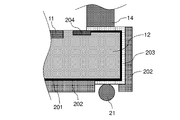


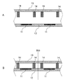

Classifications
-
- H—ELECTRICITY
- H01—ELECTRIC ELEMENTS
- H01L—SEMICONDUCTOR DEVICES NOT COVERED BY CLASS H10
- H01L23/00—Details of semiconductor or other solid state devices
- H01L23/02—Containers; Seals
-
- H—ELECTRICITY
- H01—ELECTRIC ELEMENTS
- H01L—SEMICONDUCTOR DEVICES NOT COVERED BY CLASS H10
- H01L27/00—Devices consisting of a plurality of semiconductor or other solid-state components formed in or on a common substrate
- H01L27/14—Devices consisting of a plurality of semiconductor or other solid-state components formed in or on a common substrate including semiconductor components sensitive to infrared radiation, light, electromagnetic radiation of shorter wavelength or corpuscular radiation and specially adapted either for the conversion of the energy of such radiation into electrical energy or for the control of electrical energy by such radiation
- H01L27/144—Devices controlled by radiation
- H01L27/146—Imager structures
-
- H—ELECTRICITY
- H01—ELECTRIC ELEMENTS
- H01L—SEMICONDUCTOR DEVICES NOT COVERED BY CLASS H10
- H01L31/00—Semiconductor devices sensitive to infrared radiation, light, electromagnetic radiation of shorter wavelength or corpuscular radiation and specially adapted either for the conversion of the energy of such radiation into electrical energy or for the control of electrical energy by such radiation; Processes or apparatus specially adapted for the manufacture or treatment thereof or of parts thereof; Details thereof
- H01L31/02—Details
Definitions
- the present invention relates to an optical semiconductor device and its manufacturing method, a solid-state imaging device, and an electronic device.
- CMOS sensors and CCD sensors are used in digital cameras and smartphones. ⁇ There is an increasing demand for higher definition.
- An optical semiconductor device has, for example, a hollow structure in which a semiconductor substrate provided with a light receiving element and a glass substrate are bonded together with an adhesive.
- a liquid adhesive such as epoxy resin or acrylic resin is applied to the periphery of a semiconductor substrate, and after a glass substrate serving as a sealing substrate is placed, the liquid adhesive is cured by heating.
- Non-Patent Document 1 the imaging characteristics of conventional optical semiconductor devices such as those described in Non-Patent Document 1 may be affected.
- optical noise specifically, flare, ghost, etc.
- the present invention has been made in view of the above problems, and its object is to provide an optical semiconductor device capable of suppressing the generation of optical noise, a manufacturing method thereof, and a solid-state imaging device and electronic equipment having the optical semiconductor device. It is to be.
- An optical semiconductor device comprises a semiconductor substrate provided with a light receiving element, a transparent substrate facing the surface of the semiconductor substrate provided with the light receiving element, and an adhesive layer bonding the semiconductor substrate and the transparent substrate.
- the adhesive layer is provided so as to surround the light receiving element.
- the refractive index of the adhesive layer is 1.60 or less.
- the angle between the surface of the transparent substrate on the semiconductor substrate side and the inner wall surface of the adhesive layer is 90° or more and 130° or less.
- the adhesive layer has a height of 15 ⁇ m or more and 300 ⁇ m or less.
- the optical semiconductor device further includes a wiring board provided on the side of the semiconductor substrate opposite to the transparent substrate side.
- the semiconductor substrate is provided with an electrode pad, and the adhesive layer is arranged between the electrode pad and the light receiving element.
- the optical semiconductor device is a chip size package type.
- the adhesive layer includes a cured layer composed of a cured photosensitive composition.
- the photosensitive composition contains a polysiloxane compound and a photopolymerization initiator, and the polysiloxane compound contains a cationically polymerizable group and an alkali and a solubilizing group.
- the cationic polymerizable group is one or more selected from the group consisting of glycidyl groups, alicyclic epoxy groups and oxetanyl groups.
- the alkali-soluble group comprises a monovalent organic group represented by the following chemical formula (X1) and a divalent organic group represented by the following chemical formula (X2). It is one or more selected from the group consisting of
- the photosensitive composition further contains a compound having a radically polymerizable group, and contains a radical photopolymerization initiator as the photopolymerization initiator.
- a solid-state imaging device according to the present invention has an optical semiconductor device according to the present invention.
- An electronic device has a solid-state imaging device according to the present invention.
- a method for manufacturing an optical semiconductor device includes an adhesive layer forming step, a lamination step, and a curing step.
- the adhesive layer forming step a patterned adhesive layer is formed on the transparent substrate.
- the transparent substrate provided with the adhesive layer and the semiconductor substrate provided with the light receiving element are provided on the surface of the transparent substrate provided with the adhesive layer and the light receiving element of the semiconductor substrate.
- Lamination is performed so that the surfaces facing each other are opposite to each other.
- the adhesive layer is cured to bond the transparent substrate and the semiconductor substrate.
- the adhesive layer is arranged around the light receiving element. The refractive index of the adhesive layer after curing is 1.60 or less.
- a film made of a photosensitive composition is patterned in a semi-cured state by photolithography.
- the adhesive layer forming step after exposing the film composed of the photosensitive composition through soda lime glass, the film after exposure to develop.
- the photosensitive composition contains a polysiloxane compound, a photoradical polymerization initiator, and a compound having a radically polymerizable group, and the polysiloxane A compound has a cationic polymerizable group and an alkali-soluble group in one molecule.
- an optical semiconductor device capable of suppressing the generation of optical noise, a manufacturing method thereof, and a solid-state imaging device and electronic equipment having the optical semiconductor device.
- FIG. 3 is a partially enlarged cross-sectional view showing another example of the optical semiconductor device according to the present invention
- FIG. 4 is a cross-sectional view showing another example of the optical semiconductor device according to the present invention
- FIG. 3 is a partially enlarged cross-sectional view showing another example of the optical semiconductor device according to the present invention
- FIG. 3 is a partially enlarged cross-sectional view showing another example of the optical semiconductor device according to the present invention
- FIG. 4 is a cross-sectional view showing another example of the optical semiconductor device according to the present invention
- FIG. 4 is a plan view showing a transparent substrate after formation of an adhesive layer in manufacturing an example of an optical semiconductor device according to the present invention
- FIG. 4 is a plan view showing a transparent substrate after formation of an adhesive layer in manufacturing an example of an optical semiconductor device according to the present invention
- FIG. 4 is a plan view showing a transparent substrate after singulation when manufacturing an example of the optical semiconductor device according to the present invention
- 4A, 4B, and 4C are cross-sectional views showing an example of a step of forming an adhesive layer when manufacturing an optical semiconductor device according to the present invention
- FIG. 4A, 4B, and 4C are cross-sectional views showing an example of a stacking step and a curing step when manufacturing an optical semiconductor device according to the present invention
- FIG. FIG. 4 is a plan view showing a semiconductor substrate after light receiving elements are formed when manufacturing an example of an optical semiconductor device according to the present invention
- 4A and 4B are cross-sectional views showing another example of the lamination process when manufacturing the optical semiconductor device according to the present invention
- FIG. FIG. 2 is a plan view showing an example of a printing mask used when forming an adhesive layer by screen printing;
- Refractive index refers to the refractive index for light with a wavelength of 404 nm in an atmosphere at a temperature of 23°C.
- the method for measuring the refractive index is the same method as in Examples described later or a method based thereon.
- a “polysiloxane compound” is a compound having a polysiloxane structure composed of siloxane units (Si--O--Si).
- the polysiloxane structure includes a chain polysiloxane structure (specifically, a linear polysiloxane structure, a branched polysiloxane structure, etc.) and a cyclic polysiloxane structure.
- a “photopolymerization initiator” refers to a compound that generates active species (specifically, radicals, cations, anions, etc.) upon exposure to active energy rays.
- a “radical photopolymerization initiator” refers to a compound that generates radicals as active species upon irradiation with active energy rays.
- the term “photocationic polymerization initiator” refers to a compound that generates cations (acids) as active species upon irradiation with active energy rays.
- Active energy rays include visible light, ultraviolet rays, infrared rays, electron beams, X-rays, ⁇ rays, ⁇ rays, ⁇ rays, and the like.
- a “cationic polymerizable group” refers to a functional group that polymerizes in a chain in the presence of a cation.
- alkali-soluble group refers to a functional group that enhances solubility in alkaline solutions by interacting or reacting with alkali.
- alicyclic epoxy group refers to a functional group formed by bonding one oxygen atom to two adjacent carbon atoms among the carbon atoms constituting an alicyclic structure. , 4-epoxycyclohexyl group and the like.
- a “radical polymerizable group” refers to a functional group having a radically polymerizable unsaturated bond.
- Solid content is a non-volatile component in the composition, and “total solid content” means the total amount of constituent components of the composition excluding the solvent.
- system may be added after the name of the compound to generically refer to the compound and its derivatives.
- name of a polymer when the name of a polymer is expressed by adding "system” to the name of a compound, it means that the repeating unit of the polymer is derived from the compound or its derivative.
- acryl and methacryl may be collectively referred to as "(meth)acryl”.
- acrylates and methacrylates may be collectively referred to as "(meth)acrylates”.
- acryloyl and methacryloyl may be collectively referred to as "(meth)acryloyl”.
- the adhesive layer after curing may be simply referred to as "adhesive layer”.
- An optical semiconductor device includes a semiconductor substrate provided with a light receiving element, a transparent substrate facing the surface of the semiconductor substrate provided with the light receiving element, and an adhesive for bonding the semiconductor substrate and the transparent substrate. Have a layer.
- the adhesive layer is provided so as to surround the light receiving element.
- the refractive index of the adhesive layer is 1.60 or less.
- the optical semiconductor device according to the first embodiment can suppress the generation of optical noise. The reason is presumed as follows.
- the adhesive layer has a refractive index of 1.60 or less, the light reflectance on the adhesive layer surface (specifically, the inner wall surface of the adhesive layer) is relatively low. Therefore, in the optical semiconductor device according to the first embodiment, the amount of reflected light (more specifically, reflected light from the inner wall surface of the adhesive layer) incident on the light receiving element is relatively small. optical noise is less likely to occur. Therefore, the optical semiconductor device according to the first embodiment can suppress the generation of optical noise.
- optical semiconductor device 10 shown in FIG. 1
- FIG. 3 a wiring substrate
- FIG. 3 a chip size package type optical semiconductor device
- FIG. 1 is a cross-sectional view showing an optical semiconductor device 10 as a specific example of the optical semiconductor device according to the first embodiment.
- An optical semiconductor device 10 shown in FIG. 1 includes a semiconductor substrate 12 , a transparent substrate 13 and an adhesive layer 14 .
- a light receiving element 11 is provided on the first surface 12 a of the semiconductor substrate 12 .
- the optical semiconductor device 10 further includes a wiring substrate 17 (interposer) bonded to the second surface 12b of the semiconductor substrate 12 (the side of the semiconductor substrate 12 opposite to the transparent substrate 13 side) via a die bonding material 18.
- the “first surface 12a of the semiconductor substrate 12” means one surface of two surfaces orthogonal to the thickness direction of the semiconductor substrate 12. As shown in FIG.
- the “second surface 12b of the semiconductor substrate 12” means the other surface of the two surfaces of the semiconductor substrate 12 perpendicular to the thickness direction.
- the transparent substrate 13 is arranged to face the first surface 12 a of the semiconductor substrate 12 .
- the adhesive layer 14 is a layer that bonds the semiconductor substrate 12 and the transparent substrate 13 together and is provided so as to surround the light receiving element 11 .
- the adhesive layer 14 has, for example, a square tubular structure (see FIG. 8).
- Semiconductor substrate electrode pads 15 and wiring substrate electrode pads 16 are provided on the semiconductor substrate 12 and the wiring substrate 17, respectively.
- the semiconductor substrate electrode pads 15 and the wiring substrate electrode pads 16 are electrically connected via metal wires 19 .
- the adhesive layer 14 is arranged between the semiconductor substrate electrode pad 15 and the light receiving element 11 , and the peripheral portion (the area including the wire 19 ) of the adhesive layer 14 is sealed with a sealing resin 20 .
- Solder balls 21 are formed on the surface of the wiring board 17 opposite to the die bonding material 18 side.
- the internal space Z surrounded by the semiconductor substrate 12, the transparent substrate 13, and the adhesive layer 14 may be a closed space.
- the adhesive layer 14 functions as a partition that prevents entry of moisture and dust into the effective pixel area.
- the adhesive layer 14 is formed with air holes, foreign matter can be prevented from entering the internal space Z by forming the adhesive layer 14 in a labyrinthine manner.
- the refractive index of the adhesive layer 14 is preferably 1.60 or less, more preferably 1.55 or less, and even more preferably 1.53 or less.
- the lower limit of the refractive index of the adhesive layer 14 is not particularly limited, it is, for example, 1.30.
- the refractive index of the adhesive layer 14 can be adjusted by changing the constituent material of the adhesive layer 14 .
- the refractive index of the adhesive layer 14 can be easily adjusted to 1.60 or less.
- the refractive index of the adhesive layer 14 can be adjusted by using a filler, which will be described later, as a constituent material of the adhesive layer 14 .
- the constituent material of the adhesive layer 14 is not particularly limited as long as it can be adjusted to have a refractive index of 1.60 or less.
- a cured product of a photosensitive composition is preferable from the viewpoint of ease of conversion. That is, from the viewpoint of ease of patterning, the adhesive layer 14 is preferably a cured layer composed of a cured photosensitive composition.
- photosensitive compositions it is possible to use photosensitive compositions such as cationic curable epoxy resin compositions and radical curable acrylic resin compositions. Photosensitive compositions are preferred. The details of the photosensitive composition will be described later.
- the adhesive layer 14 is The height H is preferably 500 ⁇ m or less, more preferably 400 ⁇ m or less, even more preferably 300 ⁇ m or less, even more preferably 150 ⁇ m or less, 140 ⁇ m or less, 130 ⁇ m or less, 120 ⁇ m or less, It may be 110 ⁇ m or less or 100 ⁇ m or less.
- the height H of the adhesive layer 14 is preferably 10 ⁇ m or more, more preferably 12 ⁇ m or more. It is more preferably 15 ⁇ m or more, even more preferably 20 ⁇ m or more, and may be 25 ⁇ m or more or 30 ⁇ m or more.
- the height H of the adhesive layer 14 is preferably 15 ⁇ m or more and 300 ⁇ m or less, and 20 ⁇ m or more. It is more preferably 150 ⁇ m or less, still more preferably 30 ⁇ m or more and 150 ⁇ m or less, even more preferably 30 ⁇ m or more and 120 ⁇ m or less, and particularly preferably 30 ⁇ m or more and 100 ⁇ m or less.
- the height H of the adhesive layer 14 has little variation. Specifically, the variation in the height H of the adhesive layer 14 is within 20% of the average value of the height H of the adhesive layer 14 (for example, the average value of 10 randomly selected measurement points). It is preferably within 10%, more preferably within 10%.
- the adhesive layer 14 has a square tubular structure (see FIG. 8), it is preferable that the four corners of the adhesive layer 14 are curved.
- the four corners of the adhesive layer 14 are curved, stress concentration on the four corners is alleviated during solder reflow and thermal shock tests, and peeling and cracking of the adhesive layer 14 can be reduced.
- the radius of curvature of each of the four corners of the adhesive layer 14 should be 0.01 mm or more. It is preferably 0 mm or less.
- the surface of the adhesive layer 14 may have steps in both the horizontal and vertical directions, like a corrugated shape. With such a shape, stress is relieved during solder reflow and thermal shock tests, and the reliability of the adhesive layer 14 is improved.
- the width of the adhesive layer 14 is, for example, 10 ⁇ m or more and 200 ⁇ m or less, preferably 20 ⁇ m or more and 150 ⁇ m or less.
- An example of the semiconductor substrate 12 is an image sensor substrate.
- the thickness of the semiconductor substrate 12 is, for example, 50 ⁇ m or more and 800 ⁇ m or less.
- the transparent substrate 13 for example, a glass substrate, a transparent plastic substrate (more specifically, an acrylic resin substrate, a polycarbonate substrate, etc.) can be used, and a glass substrate is preferable from the viewpoint of reliability.
- a glass substrate is preferable from the viewpoint of reliability.
- the type of glass is not particularly limited, quartz glass, borosilicate glass, alkali-free glass, and the like can be mentioned.
- the thickness of the transparent substrate 13 is, for example, 50 ⁇ m or more and 2000 ⁇ m or less.
- Infrared reflection film or infrared cut filter
- antireflection film AR coat
- antireflection film protective film
- reinforced film shielding film
- conductive film antistatic film
- low pass A coating film having a function such as a filter, a high-pass filter, a band-pass filter, etc. may be formed.
- antireflection films and infrared reflective films are preferable because they reduce optical noise in captured images.
- the coating film include silica (SiO 2 ), titanium oxide (TiO 2 ), alumina (Al 2 O 3 ), zirconia (ZrO 2 ), tantalum oxide (Ta 2 O 5 ), niobium oxide (Nb 2 O 5 ), lanthanum oxide (La 2 O 3 ), yttrium oxide (Y 2 O 3 ), magnesium oxide (MgO), hafnium oxide (HfO 2 ), chromium oxide (Cr 2 O 3 ), magnesium fluoride (MgF 2 ), molybdenum oxide ( MoO3 ), tungsten oxide (WO3) , cerium oxide (CeO2), vanadium oxide (VO2), titanium zirconium oxide ( ZrTiO4 ), zinc sulfide (ZnS), cryolite ( Na3 AlF 6 ), thiolite (Na 5 Al 3 F 14 ), yttrium fluoride (YF 3 ), calcium fluoride (CaF 2 ), si
- an antireflection film TiO 2 , Nb 2 O 5 , Ta 2 O 5 , CaF 2 , SiO 2 , Al 2 O 3 , MgS 2 , ZrO 2 , NiO and MgF 2 It is preferable to use a multilayer film containing one or more inorganic materials selected from the group consisting of
- These coating films can be provided on both sides or one side of the transparent substrate 13 .
- the types of coating films may be the same or different. It is also possible to laminate different coating films having the same function on one surface. It is also possible to stack different coating films having different functions on one surface.
- the number of layers to be laminated is not particularly limited, either, and the multilayer can be several to several tens of layers.
- a plurality of photodiodes are formed in the light receiving element 11 .
- a color filter layer (not shown) and a microlens (not shown) are formed on the photodiodes.
- the color filters are partitioned so as to correspond to individual photodiodes and are colored with one of the three primary colors of light.
- the microlens has a hemispherical shape and converges incident light onto individual photodiodes.
- thermosetting resins such as epoxy resins and silicone resins that are less likely to deteriorate during reflow at a temperature of about 260°C are preferable.
- the wiring board 17 is a multilayer wiring board having a glass epoxy resin base material or the like and metal wiring, and wiring and interlayer connection vias are formed on its surface and inside.
- Wiring board electrode pads 16 for connecting with semiconductor board electrode pads 15 on the semiconductor board 12 by wires 19 are arranged on the surface of the wiring board 17 on which the semiconductor board 12 is placed.
- Solder balls 21 serving as external connection terminals are formed on the surface of the wiring substrate 17 opposite to the semiconductor substrate 12 side.
- the wiring substrate 17 also has a function as a support substrate that suppresses deformation of the semiconductor substrate 12 .
- the sealing resin 20 is not particularly limited, thermosetting resins such as epoxy resins, acrylic resins, and silicone resins are preferable, and epoxy resins are preferable from the viewpoint of resin toughness and heat resistance. From the viewpoint of reducing optical noise such as flare, the sealing resin 20 is preferably colored black. From the viewpoint of handleability, the sealing resin 20 preferably contains a filler such as silica and has thixotropy before curing.
- the adhesive layer 14 has a rectangular cross-sectional structure, but the cross-sectional shape of the adhesive layer 14 is not limited to this.
- the angle TA formed by the surface 13a of the transparent substrate 13 on the semiconductor substrate 12 side and the inner wall surface 14a of the adhesive layer 14 may exceed 90°.
- the angle formed by the semiconductor substrate side surface of the transparent substrate and the inner wall surface of the adhesive layer (the angle TA in FIG. 2) may be referred to as a "taper angle".
- the taper angle should be 90° or more. Preferably, it is more than 90°, more preferably 95° or more, even more preferably 100° or more, and may be 110° or more. Further, in order to obtain a highly reliable optical semiconductor device by ensuring a sufficient bonding area between the adhesive layer 14 and the semiconductor substrate 12, the taper angle is preferably 130° or less, more preferably 125° or less. is more preferably 120° or less.
- the taper angle is preferably 90° or more and 130° or less, more preferably 90° or more and 125° or less. It is more preferably 95° or more and 125° or less, even more preferably 100° or more and 125° or less, and may be 100° or more and 120° or less or 110° or more and 120° or less.
- Optical semiconductor device 100 Next, as another specific example of the optical semiconductor device according to the first embodiment, a chip size package type (CSP type) optical semiconductor device 100 will be described with reference to the drawings. In the following description, the description of the content that overlaps with the optical semiconductor device 10 may be omitted.
- CSP type chip size package type
- FIG. 3 is a cross-sectional view showing the optical semiconductor device 100.
- the optical semiconductor device 100 includes a semiconductor substrate 12 having a light receiving element 11 provided on the first surface 12a, a transparent substrate 13, and an adhesive layer 14 for bonding the semiconductor substrate 12 and the transparent substrate 13 together. It is the same as the optical semiconductor device 10 . Further, in the optical semiconductor device 100, the transparent substrate 13 is arranged to face the first surface 12a of the semiconductor substrate 12, and the adhesive layer 14 is provided so as to surround the light receiving element 11. Same as device 10 .
- the width of the optical semiconductor device 100 and the width of the semiconductor substrate 12 are substantially equal.
- the optical semiconductor device 100 does not have the wiring board, wiring board electrode pads, and wires that the optical semiconductor device 10 has, sealing with a sealing resin is unnecessary.
- the second surface 12b of the semiconductor substrate 12 is provided with solder balls 21 as external connection terminals.
- the optical semiconductor device 100 has the advantage that the device can be miniaturized by adopting the CSP type structure. Since the optical semiconductor device 100 does not have a wiring board, it is necessary to electrically connect the semiconductor substrate 12 and the solder balls 21 separately. Examples of methods for electrically connecting the semiconductor substrate 12 and the solder balls 21 will be described below, but the method is not limited to these.
- a method for the electrical connection for example, there is a method of providing a through silicon via 200 as shown in FIG.
- an insulating layer 201, a rewiring layer 203, and a solder resist 202 are provided in this order on the surface of the semiconductor substrate 12 opposite to the adhesive layer 14 side.
- the solder balls 21 are formed in openings of the solder resist 202 and electrically connected to electrode pads 204 formed on the surface of the semiconductor substrate 12 on the adhesive layer 14 side through the rewiring layer 203 .
- the insulating layer 201 is not particularly limited as long as it is made of a material having high insulating properties. Hydrogen Silsesquioxane) membrane, MSQ (Methyl Silsesquioxane) membrane, and the like. Moreover, as a method for forming the insulating layer 201, a CVD method, a coating method, or the like can be used.
- the solder resist 202 is not particularly limited as long as it is a material having heat resistance and insulation properties during mounting, but examples include epoxy resins and acrylic resins, among which epoxy resins are preferred from the viewpoint of high heat resistance and insulation properties. Photolithography, screen printing, and the like are examples of methods for forming the solder resist 202 .
- the material of the rewiring layer 203 is not particularly limited as long as it is a conductive material, but copper (Cu), aluminum (Al), tungsten (W), gold (Au), titanium (Ti), nickel (Ni ) and the like.
- a wet etching method, a dry etching method, a lift-off method, or the like can be used as a method for forming the rewiring layer 203.
- FIG. 1 A method of electrically connecting the ball 21 and the electrode pad 204 can be mentioned.
- optical semiconductor device 100 Other points of the optical semiconductor device 100 are the same as those described in the section [Optical semiconductor device 10] above.
- the present invention is not limited to the example described above.
- the optical semiconductor device according to the present invention may have a laminated structure with two or more adhesive layers.
- An optical semiconductor device 300 shown in FIG. 6 is an example of an optical semiconductor device having a laminated structure with two or more adhesive layers.
- the adhesive layer 14 has a first adhesive layer 141 and a second adhesive layer 142 in order from the transparent substrate 13 side.
- the first adhesive layer 141 is a cured layer made of, for example, a cured product of a specific photosensitive composition which will be described later.
- the second adhesive layer 142 is, for example, a cured layer composed of a cured liquid adhesive (more specifically, a cured layer formed by curing the liquid adhesive without patterning it).
- the height of the adhesive layer means the sum of the heights of the layers constituting the adhesive layer (total height). . Moreover, in the case of an optical semiconductor device having a laminated structure of two or more adhesive layers, it is preferable that each layer constituting the adhesive layer has a refractive index of 1.60 or less.
- photosensitive composition that can be used as a material for the adhesive layer of the optical semiconductor device according to the first embodiment.
- a photosensitive composition that can be used as a material for the adhesive layer when irradiated with an active energy ray, the photosensitive group is crosslinked by cations or radicals generated from the photopolymerization initiator, and the curing reaction proceeds. It is not particularly limited as long as it is a composition.
- photosensitive groups include cationically polymerizable groups such as epoxy groups, oxetanyl groups, vinyl ether groups, and alkoxysilyl groups, and radically polymerizable groups having radically polymerizable unsaturated bonds.
- radically polymerizable groups include (meth)acryloyl groups and vinyl groups.
- the photosensitive group-containing compound contained in the photosensitive composition may have both a cationically polymerizable group and a radically polymerizable group in one molecule, or may have only one of them.
- a compound having a cationic polymerizable group and a compound having a radically polymerizable group may be used in combination.
- the photosensitive composition preferably contains a polysiloxane compound.
- Preferred examples of the photosensitive composition containing the polysiloxane compound are described below.
- a photosensitive composition preferable as a material for the adhesive layer is a polysiloxane compound having a cationic polymerizable group and an alkali-soluble group in one molecule (hereinafter referred to as It contains a “component (A)”) and a photopolymerization initiator (hereinafter sometimes referred to as “component (B)").
- Component (A) is not particularly limited as long as it is a polysiloxane compound having a cationic polymerizable group and an alkali-soluble group in one molecule.
- Component (A) has a cationic polymerizable group and an alkali-soluble group in one molecule, it is possible to obtain a specific photosensitive composition which is excellent in both developability and curability.
- Component (A) preferably has a plurality of cationic polymerizable groups in one molecule.
- component (A) has a plurality of cationically polymerizable groups in one molecule, an adhesive layer having a high crosslink density is obtained, and as a result, the heat resistance of the adhesive layer tends to be further improved.
- the plurality of cationically polymerizable groups may be of the same type or may be two or more different functional groups.
- component (A) preferably has a plurality of alkali-soluble groups in one molecule.
- the plurality of alkali-soluble groups may be of the same kind or may be two or more different functional groups.
- Component (A) may have a chain polysiloxane structure or a cyclic polysiloxane structure.
- Component (A) preferably has a cyclic polysiloxane structure in order to form an adhesive layer with better heat resistance.
- the specific photosensitive composition tends to have high film-forming properties and developability.
- the component (A) may have a polysiloxane structure in its main chain and may have a polysiloxane structure in its side chains.
- component (A) preferably has a polysiloxane structure in its main chain.
- component (A) preferably has a cyclic polysiloxane structure in its main chain.
- the cyclic polysiloxane structure may be a monocyclic structure or a polycyclic structure.
- the polycyclic structure may be a polyhedral structure.
- T units XSiO 3/2
- Q units SiO 4/2
- M units X 3 SiO 1/2
- D units X 2 SiO 2/2
- the weight average molecular weight of the polymer is preferably 10,000 or more and 50,000 or less, more preferably 20,000 or more and 40,000 or less.
- the weight average molecular weight is 10,000 or more, the heat resistance of the obtained adhesive layer tends to be further improved.
- the weight average molecular weight is 50,000 or less, the developability tends to be further improved.
- Examples of cationically polymerizable groups possessed by component (A) include epoxy groups, vinyl ether groups, oxetanyl groups, and alkoxysilyl groups.
- the cationically polymerizable group is preferably one or more selected from the group consisting of a glycidyl group, an alicyclic epoxy group and an oxetanyl group. More preferably, one or more selected from the group consisting of epoxy groups.
- an alicyclic epoxy group is particularly preferable because of its excellent cationic photopolymerizability.
- Examples of the alkali-soluble group that the component (A) has include a monovalent organic group represented by the following chemical formula (X1) (hereinafter sometimes referred to as “X1 group”) and a chemical formula (X2) below.
- divalent organic groups hereinafter sometimes referred to as "X2 groups”
- X1 group is a monovalent organic group derived from N-monosubstituted isocyanuric acid.
- the X2 group is a divalent organic group derived from N,N'-disubstituted isocyanuric acid.
- the alkali-soluble group contained in component (A) is preferably one or more selected from the group consisting of X1 group and X2 group.
- component (A) is preferably a polysiloxane compound that has been organically modified by a hydrosilylation reaction and into which cationic polymerizable groups have been introduced via silicon-carbon bonds.
- the alkali-soluble group is also preferably introduced into the polysiloxane compound through a silicon-carbon bond by a hydrosilylation reaction.
- Component (A) can be obtained, for example, by a hydrosilylation reaction using the following compound ( ⁇ ), compound ( ⁇ ) and compound ( ⁇ ) as starting materials.
- ⁇ Compound ( ⁇ ) A polysiloxane compound having at least two SiH groups (hydrosilyl groups) in one molecule
- ⁇ Compound ( ⁇ ) A carbon-carbon double bond having reactivity with SiH groups in one molecule and a cationic polymerizable group/compound ( ⁇ ): a compound having a carbon-carbon double bond reactive with an SiH group and an alkali-soluble group in one molecule
- Compound ( ⁇ ) is a polysiloxane compound having at least two SiH groups in one molecule, for example, the compound described in WO 96/15194, which has at least two SiH groups in one molecule. You can use what you have.
- Specific examples of the compound ( ⁇ ) include a hydrosilyl group-containing polysiloxane having a linear structure, a polysiloxane having a hydrosilyl group at the molecular end, and a cyclic polysiloxane having a hydrosilyl group (hereinafter simply referred to as “cyclic polysiloxane”). sometimes), etc.
- the cyclic polysiloxane may have a polycyclic structure, and the polycyclic structure may be a polyhedral structure.
- a cyclic polysiloxane having at least two SiH groups in one molecule as the compound ( ⁇ ).
- Compound ( ⁇ ) is preferably a cyclic polysiloxane having 3 or more SiH groups in one molecule.
- the group present on the Si atom is preferably either a hydrogen atom or a methyl group.
- hydrosilyl group-containing polysiloxanes having a linear structure examples include copolymers of dimethylsiloxane units, methylhydrogensiloxane units and terminal trimethylsiloxy units, and copolymers of diphenylsiloxane units, methylhydrogensiloxane units and terminal trimethylsiloxy units.
- examples include polymers, copolymers of methylphenylsiloxane units, methylhydrogensiloxane units and terminal trimethylsiloxy units, and polysiloxanes whose ends are blocked with dimethylhydrogensilyl groups.
- polysiloxanes having hydrosilyl groups at their molecular terminals include polysiloxanes whose terminals are blocked with dimethylhydrogensilyl groups, dimethylhydrogensiloxane units (H(CH 3 ) 2 SiO 1/2 units), and SiO 2 units. , SiO 3/2 units and one or more siloxane units selected from the group consisting of SiO units.
- the cyclic polysiloxane is represented, for example, by the following general formula (I).
- R 1 , R 2 and R 3 each independently represent a monovalent organic group having 1 to 20 carbon atoms
- m represents an integer of 2 to 10
- n is It represents an integer of 0 or more and 10 or less.
- m is preferably 3 or more.
- m+n is preferably 3 or more and 12 or less.
- n is 0 in order to facilitate the hydrosilylation reaction.
- R 1 , R 2 and R 3 are preferably organic groups composed of elements selected from the group consisting of C, H and O.
- R 1 , R 2 and R 3 include alkyl groups, hydroxyalkyl groups, alkoxyalkyl groups, oxyalkyl groups, aryl groups and the like. Among them, chain alkyl groups such as methyl group, ethyl group, propyl group, hexyl group, octyl group, decyl group and dodecyl group; cyclic alkyl groups such as cyclohexyl group and norbornyl group; and phenyl group are preferable.
- R 1 , R 2 and R 3 are preferably chain alkyl groups having 1 to 6 carbon atoms or phenyl groups.
- each of R 1 , R 2 and R 3 is preferably a chain alkyl group, more preferably a chain alkyl group having 1 to 6 carbon atoms, and still more preferably a methyl group. .
- Cyclic polysiloxanes represented by general formula (I) include 1,3,5,7-tetrahydrogen-1,3,5,7-tetramethylcyclotetrasiloxane, 1-propyl-3,5,7 -trihydrogen-1,3,5,7-tetramethylcyclotetrasiloxane, 1,5-dihydrogen-3,7-dihexyl-1,3,5,7-tetramethylcyclotetrasiloxane, 1,3 ,5-trihydrogen-1,3,5-trimethylcyclotrisiloxane, 1,3,5,7,9-pentahydrogen-1,3,5,7,9-pentamethylcyclopentasiloxane, and 1 , 3,5,7,9,11-hexahydrogen-1,3,5,7,9,11-hexamethylcyclohexasiloxane and the like. Among them, 1,3,5,7-tetrahydrogen-1,3,5,7-tetramethylcyclotetrasiloxane (
- the compound ( ⁇ ) is obtained by a known synthetic method.
- the cyclic polysiloxane represented by general formula (I) can be synthesized by the method described in International Publication No. 96/15194.
- a cyclic polysiloxane having a polyhedral skeleton can be synthesized, for example, by the methods described in JP-A-2004-359933, JP-A-2004-143449, JP-A-2006-269402, and the like.
- the content of the structural unit derived from the compound ( ⁇ ) in the component (A) should be 100% by weight of the component (A). is preferably 10% by weight or more and 50% by weight or less, more preferably 15% by weight or more and 45% by weight or less.
- the compound ( ⁇ ) is a compound having, in one molecule, a carbon-carbon double bond reactive with an SiH group (hydrosilyl group) and a cationically polymerizable group, and a cationically polymerizable group in the polysiloxane compound. is a compound for introducing The cationically polymerizable group in the compound ( ⁇ ) is the same as the cationically polymerizable group of the component (A) described above, and preferred embodiments are also the same.
- the compound ( ⁇ ) preferably has one or more selected from the group consisting of a glycidyl group, an alicyclic epoxy group and an oxetanyl group as a cationically polymerizable group. It is more preferable to have one or more selected from the group consisting of, more preferably to have an alicyclic epoxy group.
- alkenyl groups include, for example, vinyl groups, allyl groups, methallyl groups, allyloxy groups (- O—CH 2 —CH ⁇ CH 2 ), 2-allylphenyl group, 3-allylphenyl group, 4-allylphenyl group, 2-(allyloxy)phenyl group, 3-(allyloxy)phenyl group, 4-(allyloxy) phenyl group, 2-(allyloxy)ethyl group, 2,2-bis(allyloxymethyl)butyl group, 3-allyloxy-2,2-bis(allyloxymethyl)propyl group, vinyl ether group and the like.
- the compound ( ⁇ ) preferably has one or more alkenyl groups selected from the group consisting of vinyl groups, allyl groups and allyloxy groups. It is more preferable to have one or more selected from the group consisting of:
- the compound ( ⁇ ) examples include 1-vinyl-3,4-epoxycyclohexane, allyl glycidyl ether, allyl oxetanyl ether, diallyl monoglycidyl isocyanurate, monoallyl diglycidyl isocyanurate, and the like.
- the compound ( ⁇ ) is preferably a compound having one or more functional groups selected from the group consisting of an alicyclic epoxy group and a glycidyl group, and has an alicyclic epoxy group. Compounds are more preferred.
- the compound ( ⁇ ) is preferably one or more compounds selected from the group consisting of diallyl monoglycidyl isocyanurate and 1-vinyl-3,4-epoxycyclohexane. 1-Vinyl-3,4-epoxycyclohexane is more preferred.
- the content of the structural unit derived from the compound ( ⁇ ) in the component (A) is 100% by weight of the component (A). is preferably 20% by weight or more and 50% by weight or less, more preferably 22% by weight or more and 45% by weight or less.
- Compound ( ⁇ ) is a compound having a carbon-carbon double bond reactive with SiH groups and an alkali-soluble group in one molecule, and is a compound for introducing an alkali-soluble group into a polysiloxane compound. is.
- the alkali-soluble group in compound ( ⁇ ) is the same as the alkali-soluble group of component (A) described above, and preferred embodiments are also the same. That is, compound ( ⁇ ) preferably has, as an alkali-soluble group, one or more selected from the group consisting of X1 group and X2 group.
- the compound ( ⁇ ) has a group (alkenyl group) containing a carbon-carbon double bond that is reactive with SiH groups.
- alkenyl group possessed by the compound ( ⁇ ) include the same alkenyl groups as those exemplified as the alkenyl group possessed by the compound ( ⁇ ) described above, and preferred embodiments are also the same. That is, the compound ( ⁇ ) preferably has, as an alkenyl group, one or more selected from the group consisting of a vinyl group, an allyl group and an allyloxy group, and one selected from the group consisting of a vinyl group and an allyl group. It is more preferable to have
- the compound ( ⁇ ) may have two or more alkenyl groups in one molecule.
- compound ( ⁇ ) contains a plurality of alkenyl groups in one molecule, a plurality of compounds ( ⁇ ) can be crosslinked by hydrosilylation reaction, so that the crosslink density of the resulting cured product increases and the heat resistance of the cured product increases. tend to improve.
- the compound ( ⁇ ) include diallyl isocyanurate, monoallyl isocyanurate, 2,2′-diallyl bisphenol A, vinylphenol, allylphenol, butenoic acid, pentenoic acid, hexenoic acid, heptenoic acid, undecylenic acid, and the like. are mentioned.
- the compound ( ⁇ ) is one or more selected from the group consisting of diallyl isocyanurate, monoallyl isocyanurate and 2,2′-diallyl bisphenol A. More preferably, one or more selected from the group consisting of diallyl isocyanurate and monoallyl isocyanurate.
- component (A) having X1 group as alkali-soluble group is obtained.
- diallyl isocyanurate is used as the compound ( ⁇ )
- the component (A) having X2 group as an alkali-soluble group is obtained.
- the content of structural units derived from compound ( ⁇ ) in component (A) should be 5% by weight or more and 50% by weight with respect to 100% by weight of component (A). % or less, more preferably 10% by weight or more and 30% by weight or less.
- an alkenyl group-containing compound (hereinafter sometimes referred to as "another alkenyl group-containing compound") different from the above compounds ( ⁇ ) and ( ⁇ ) may be used.
- compound ( ⁇ ) a compound having an alkenyl group and a (meth)acryloyl group in one molecule (hereinafter referred to as "compound ( ⁇ )”) is used as another alkenyl group-containing compound. may be described) is preferably used.
- compound ( ⁇ ) a (meth)acryloyl group is introduced into the component (A), so that the component (A) can be subjected to radical photopolymerization.
- the compound ( ⁇ ) examples include vinyl acrylate, vinyl methacrylate, allyl acrylate, allyl methacrylate, 2-butenyl acrylate, 2-butenyl methacrylate, and the like.
- compound ( ⁇ ) a compound having two or more alkenyl groups in one molecule
- compound ( ⁇ ) a compound having two or more alkenyl groups in one molecule
- the number of cross-linking points increases during the hydrosilylation reaction, so that the heat resistance of the obtained adhesive layer tends to be further improved.
- the compound ( ⁇ ) include diallyl phthalate, triallyl trimellitate, diethylene glycol bisallyl carbonate, 1,1,2,2-tetraallyloxyethane, triallyl cyanurate, triallyl isocyanurate, and diallyl monobenzyl.
- the compound ( ⁇ ) is preferably one or more selected from the group consisting of triallyl isocyanurate and diallyl monomethyl isocyanurate, more preferably diallyl monomethyl isocyanurate. preferable.
- the content of the structural unit derived from the compound ( ⁇ ) in the component (A) is set to: It is preferably 5% by weight or more and 30% by weight or less, more preferably 8% by weight or more and 20% by weight or less.
- component (A) The order and method of the hydrosilylation reaction to obtain component (A) are not particularly limited.
- Component (A) is obtained by the hydrosilylation reaction.
- the component (A) obtained using the above-described compound ( ⁇ ), compound ( ⁇ ), compound ( ⁇ ), and optionally other optional starting materials is, for example, a plurality of It is a polymer having a cationic polymerizable group and a plurality of alkali-soluble groups and having a polysiloxane structure in its main chain.
- the ratio of each compound in the hydrosilylation reaction is not particularly limited, but the total amount A of alkenyl groups and the total amount B of SiH groups in the starting materials preferably satisfy 1 ⁇ B/A ⁇ 30, and 1 ⁇ It is more preferable to satisfy B/A ⁇ 10.
- Hydrosilylation catalysts such as chloroplatinic acid, platinum-olefin complexes and platinum-vinylsiloxane complexes may be used in the hydrosilylation reaction.
- a hydrosilylation catalyst and co-catalyst may be used in combination.
- the amount (amount of substance) added of the hydrosilylation catalyst is not particularly limited, but is preferably 10 ⁇ 8 times or more and 10 ⁇ 1 times or less, more preferably 10 ⁇ 6 times the total amount of alkenyl groups contained in the starting material. It is more than 10 -2 times or less.
- the reaction temperature for hydrosilylation may be appropriately set, preferably 30°C or higher and 200°C or lower, more preferably 50°C or higher and 150°C or lower.
- the oxygen concentration in the gas phase in the hydrosilylation reaction is preferably 3% by volume or less. From the viewpoint of promoting the hydrosilylation reaction, the gas phase portion may contain 0.1% by volume or more and 3% by volume or less of oxygen.
- a solvent may be used for the hydrosilylation reaction.
- a single solvent or a mixed solvent in which two or more kinds are mixed can be used.
- Solvents include hydrocarbon solvents such as benzene, toluene, xylene, hexane and heptane; ether solvents such as tetrahydrofuran, 1,4-dioxane, 1,3-dioxolane and diethyl ether; ketone solvents such as acetone and methyl ethyl ketone. ; Halogen solvents such as chloroform, methylene chloride and 1,2-dichloroethane can be used.
- Toluene, xylene, tetrahydrofuran, 1,4-dioxane, 1,3-dioxolane, or chloroform are preferred because they are easily distilled off after the reaction.
- a gelation inhibitor may be used in the hydrosilylation reaction, if desired.
- the content of component (A) in the specific photosensitive composition is It is preferably 20% by weight or more and 95% by weight or less based on the total solid content of the photosensitive composition.
- the specific photosensitive composition contains the component (A) having a cationic polymerizable group, when the specific photosensitive composition contains a photocationic polymerization initiator as the component (B), the component (A) is subjected to photocationic polymerization. can be crosslinked by Further, when using the component (A) into which a (meth)acryloyl group is introduced, or when using the component (C) described later, the specific photosensitive composition contains a photoradical polymerization initiator as the component (B). When contained, component (A) and component (C) can be crosslinked by photoradical polymerization.
- the specific photosensitive composition may contain both a photocationic polymerization initiator and a photoradical polymerization initiator as component (B).
- photocationic polymerization initiator for example, a known photocationic polymerization initiator can be used.
- photocationic polymerization initiators include various compounds that are considered suitable in JP-A-2000-1648, JP-A-2001-515533, WO 2002/83764, etc., but are not particularly limited.
- the photocationic polymerization initiator is preferably a sulfonate ester-based compound, a carboxylic acid ester-based compound or an onium salt-based compound, more preferably an onium salt-based compound, and still more preferably a sulfonium salt-based compound.
- sulfonate ester compound various sulfonic acid derivatives can be used. compounds, pyrogalloltrisulfonate-based compounds and benzylsulfonate-based compounds.
- sulfonate ester compounds include diphenyldisulfone, ditosyldisulfone, bis(phenylsulfonyl)diazomethane, bis(chlorophenylsulfonyl)diazomethane, bis(xylylsulfonyl)diazomethane, phenylsulfonylbenzoyldiazomethane, and bis(cyclohexylsulfonyl).
- a carboxylic acid ester compound can also be used as a cationic photopolymerization initiator.
- Onium salt compounds include sulfonium salt compounds and iodonium salt compounds.
- Examples of anions possessed by sulfonium salt compounds and iodonium salt compounds include tetrafluoroborate (BF 4 ⁇ ), hexafluorophosphate (PF 6 ⁇ ), hexafluoroantimonate (SbF 6 ⁇ ), hexafluoroarsenate (AsF 6 ⁇ ), hexachloroantimonate (SbCl 6 ⁇ ), tetraphenylborate, tetrakis(trifluoromethylphenyl)borate, tetrakis(pentafluoromethylphenyl)borate, fluoroalkylfluorophosphate, perchlorate ion (ClO 4 ⁇ ) , trifluoromethanesulfonate ion (CF 3 SO 3 ⁇ ), fluorosulfonate ion (FSO 3
- the photocationic polymerization initiators are arranged in descending order of acid strength of the generated acid . as an anion, a compound containing CF 3 SO 3 - as an anion, and a compound containing HSO 4 - as an anion.
- the use of a photocationic polymerization initiator that generates an acid with a high acid strength tends to increase the residual film rate.
- the pKa of the acid generated from the photocationic polymerization initiator is preferably less than 3, more preferably less than 1.
- the content of the photocationic polymerization initiator in the specific photosensitive composition is not particularly limited. From the viewpoint of the physical property balance of the curing speed and the cured product, the content of the photocationic polymerization initiator is preferably 0.1 parts by weight or more and 20 parts by weight or less with respect to 100 parts by weight of the specific photosensitive composition, It is more preferably 0.5 parts by weight or more and 10 parts by weight or less.
- thermal cationic polymerization initiator (compound that generates cations by heat) can be blended into the specific photosensitive composition as needed.
- thermal cationic polymerization initiators include sulfonium salt compounds, iodonium salt compounds, benzothiazonium salt compounds, ammonium salt compounds, phosphonium salt compounds, etc.
- sulfonium salt compounds A benzothiazonium salt compound is preferably used.
- Photoradical polymerization initiator examples include acetophenone-based compounds, acylphosphine oxide-based compounds, benzoin-based compounds, benzophenone-based compounds, ⁇ -diketone-based compounds, biimidazole-based compounds, polynuclear quinone-based compounds, triazine-based compounds, and oximes. Ester-based compounds, titanocene-based compounds, xanthone-based compounds, thioxanthone-based compounds, ketal-based compounds, azo-based compounds, peroxides, 2,3-dialkyldione-based compounds, disulfide-based compounds, fluoroamine-based compounds, and the like.
- the photoradical polymerization initiator is preferably one or more selected from the group consisting of acetophenone-based compounds, benzophenone-based compounds, and oxime ester-based compounds, and more preferably acetophenone-based compounds.
- acetophenone compounds include 1-(4-dodecylphenyl)-2-hydroxy-2-methylpropan-1-one, 2,2-dimethoxy-2-phenylacetophenone, 2-hydroxy-2-methyl-1 -phenylpropan-1-one, 1-(4′-i-propylphenyl)-2-hydroxy-2-methylpropan-1-one, 4-(2′-hydroxyethoxy)phenyl(2-hydroxy-2- propyl)ketone, 2,2-dimethoxyacetophenone, 2,2-diethoxyacetophenone, 2-methyl-1-(4'-methylthiophenyl)-2-morpholinopropan-1-one, 2-benzyl-2-dimethyl Amino-1-(4'-morpholinophenyl)butan-1-one, 1-hydroxycyclohexylphenyl ketone and the like can be mentioned.
- acylphosphine oxide compounds include 2,4,6-trimethylbenzoyl-diphenylphosphine oxide and bis(2,4,6-trimethylbenzoyl)-phenylphosphine oxide.
- oxime ester compounds examples include 1,2-octanedione 1-[4-(phenylthio)-2-(O-benzoyloxime)], ethanone 1-[9-ethyl-6-(2-methylbenzoyl) -9H-carbazol-3-yl]-1-(O-acetyloxime) and the like.
- Benzoin-based compounds include, for example, benzoin, benzoin methyl ether, benzoin ethyl ether, benzoin isopropyl ether, and benzoin isobutyl ether.
- benzophenone-based compounds include benzyldimethylketone, benzophenone, 4,4'-bis(dimethylamino)benzophenone, 4,4'-bis(diethylamino)benzophenone, and the like.
- ⁇ -diketone compounds examples include methylbenzoylformate.
- biimidazole compounds include 2,2'-bis(2-chlorophenyl)-4,4',5,5'-tetrakis(4-ethoxycarbonylphenyl)-1,2'-biimidazole, 2, 2'-bis(2,4-dichlorophenyl)-4,4',5,5'-tetrakis(4-ethoxycarbonylphenyl)-1,2'-biimidazole, 2,2'-bis(2,4, 6-trichlorophenyl)-4,4′,5,5′-tetrakis(4-ethoxycarbonylphenyl)-1,2′-biimidazole, 2,2′-bis(2-bromophenyl)-4,4′ , 5,5′-tetrakis(4-ethoxycarbonylphenyl)-1,2′-biimidazole, 2,2′-bis(2,4-dibromophenyl)-4,4′,5,5′-t
- polynuclear quinone compounds examples include anthraquinone, 2-ethylanthraquinone, 2-t-butylanthraquinone, 1,4-naphthoquinone, and the like.
- xanthone-based compounds examples include xanthone, thioxanthone, and 2-chlorothioxanthone.
- triazine compounds examples include 1,3,5-tris(trichloromethyl)-s-triazine, 1,3-bis(trichloromethyl)-5-(2′-chlorophenyl)-s-triazine, 1,3 -bis(trichloromethyl)-5-(4'-chlorophenyl)-s-triazine, 1,3-bis(trichloromethyl)-5-(2'-methoxyphenyl)-s-triazine, 1,3-bis( trichloromethyl)-5-(4'-methoxyphenyl)-s-triazine, 2-(2'-furylethylidene)-4,6-bis(trichloromethyl)-s-triazine, 2-(4'-methoxystyryl )-4,6-bis(trichloromethyl)-s-triazine, 2-(3′,4′-dimethoxystyryl)-4,6-bis(trichloromethyl
- the content of the photoradical polymerization initiator in the specific photosensitive composition is not particularly limited. From the viewpoint of the curing speed and physical property balance of the cured product, the content of the photoradical polymerization initiator is preferably 0.1 parts by weight or more and 20 parts by weight or less with respect to 100 parts by weight of the specific photosensitive composition. It is more preferably 0.5 parts by weight or more and 10 parts by weight or less.
- thermal radical polymerization initiator (a compound that generates radicals by heat) can be blended into the specific photosensitive composition as needed.
- thermal radical polymerization initiators include acetyl peroxide, benzoyl peroxide, methyl ethyl ketone peroxide, cyclohexanone peroxide, hydrogen peroxide, t-butyl hydroperoxide, cumene hydroperoxide, and di-t-butyl peroxide.
- thermal radical polymerization initiators may be used alone or in combination of two or more.
- the specific photosensitive composition may contain a solvent.
- the specific photosensitive composition can be obtained by dissolving or dispersing the components (A) and (B) described above, and optionally other components described below, in a solvent.
- solvents include hydrocarbon solvents such as benzene, toluene, hexane and heptane; ether solvents such as tetrahydrofuran, 1,4-dioxane, 1,3-dioxolane and diethyl ether; acetone, methyl ethyl ketone and methyl isobutyl ketone.
- ketone solvents such as cyclohexanone
- glycol solvents such as propylene glycol 1-monomethyl ether 2-acetate, diethylene glycol dimethyl ether, diethylene glycol ethyl methyl ether, ethylene glycol diethyl ether
- ester solvents such as isobutyl isobutyrate
- chloroform methylene chloride
- examples include halogen-based solvents such as 1,2-dichloroethane.
- the solvent is preferably an ester solvent, and more preferably isobutyl isobutyrate.
- the amount of the solvent is preferably 0.5 parts by weight or more and 100 parts by weight or less with respect to 100 parts by weight of the component (A). , more preferably 1 part by weight or more and 50 parts by weight or less.
- the specific photosensitive composition contains components (other components) other than the above components (A) and (B) as solids (components other than the solvent) within a range that does not impair the object and effect of the present invention.
- the total content of component (A) and component (B) must be It is preferably 50% by weight or more, more preferably 60% by weight or more, and still more preferably 70% by weight or more and 100% by weight or less, relative to the total solid content of the specific photosensitive composition.
- Other components include compounds having radically polymerizable groups, reactive diluents, sensitizers, polymer dispersants, thermoplastic resins, fillers, basic compounds, adhesion improvers, coupling agents (silane cup ring agents, etc.), antioxidants, radical inhibitors, mold release agents, flame retardants, flame retardant aids, surfactants, antifoaming agents, emulsifiers, leveling agents, anti-repellent agents, ion trapping agents (antimony-bismuth, etc.) ), thixotropic agent, tackifier, storage stability improver, antiozonant, light stabilizer, thickener, plasticizer, heat stabilizer, conductivity imparter, antistatic agent, radiation shielding agent , nucleating agents, phosphorus-based peroxide decomposers, lubricants, metal deactivators, thermal conductivity imparting agents, physical property modifiers, and the like.
- the specific photosensitive composition may contain a compound having a radically polymerizable group (hereinafter sometimes referred to as "component (C)”) as another component. Since component (C) is another component (a component other than components (A) and (B)), it is a compound that has a radically polymerizable group and does not have a siloxane unit.
- component (C) is another component (a component other than components (A) and (B)), it is a compound that has a radically polymerizable group and does not have a siloxane unit.
- the specific photosensitive composition containing the component (C) tends to be excellent in deep-part curability (property capable of photocrosslinking to deep parts) during patterning.
- the taper angle can be easily adjusted to a range of more than 90°.
- the taper angle can be adjusted to a range of more than 90°.
- the photosensitive composition to be used in order to easily adjust the taper angle to 95° or more, the photosensitive composition to be used must contain the component (A), the component It is preferably a photosensitive composition containing (B) and component (C) and containing a photoradical polymerization initiator as component (B).
- component (C) examples include compounds having radically polymerizable unsaturated bonds (ethylenically unsaturated bonds, etc.).
- a (meth)acryloyl group, a vinyl group, etc. are mentioned as an ethylenically unsaturated bond.
- component (C) examples include allyl (meth)acrylate, vinyl (meth)acrylate, dicyclopentenyl (meth)acrylate, dicyclopentenyloxyethyl (meth)acrylate, and (meth)acrylate-modified allylglycidyl.
- Ether (“Denacol (registered trademark) acrylate DA111" manufactured by Nagase ChemteX Corporation), urethane (meth)acrylate compound, epoxy (meth)acrylate compound, trimethylolpropane tri(meth)acrylate, pentaerythritol tetra(meth)acrylate , ditrimethylolpropane tetra(meth)acrylate, dipentaerythritol hexa(meth)acrylate, butanediol di(meth)acrylate, nonanediol di(meth)acrylate, polypropylene glycol (meth)acrylate, bisphenol A di(meth)acrylate, and tris(2-(meth)acryloyloxyethyl)isocyanurate.
- component (C) since component (C) has high curability, it is also suitable as a material for a photosensitive composition when patterning is performed by methods other than photolithography (for example, screen printing, 3D printing, etc.).
- the content of component (C) in the specific photosensitive composition is It is preferably 1% by weight or more and 50% by weight or less, more preferably 5% by weight or more and 40% by weight or less, and even more preferably 10% by weight or more and 30% by weight or less.
- the specific photosensitive composition may contain a reactive diluent.
- a reactive diluent is a component that participates in the curing reaction while reducing the viscosity of the specific photosensitive composition.
- the reactive diluent for example, a compound having two or more cationic polymerizable groups in one molecule is used.
- the cationic polymerizable group of the reactive diluent include those exemplified as the cationic polymerizable group possessed by the component (A) described above.
- the cationically polymerizable group of the reactive diluent may be of the same type as the cationically polymerizable group of component (A), or may be of a different type.
- the reactive diluent preferably has an alicyclic epoxy group as a cationic polymerizable group.
- component (A) contains an alicyclic epoxy group as the cationically polymerizable group, and the reactive diluent has two or more alicyclic epoxy groups per molecule.
- Compounds having two or more alicyclic epoxy groups in one molecule include 3′,4′-epoxycyclohexylmethyl 3,4-epoxycyclohexane carboxylate ("Celoxide (registered trademark) 2021P” manufactured by Daicel Corporation), ⁇ -caprolactone-modified 3′,4′-epoxycyclohexylmethyl 3,4-epoxycyclohexane carboxylate ("Celoxide (registered trademark) 2081" manufactured by Daicel), bis(3,4-epoxycyclohexylmethyl) adipate, the following chemical formula ( S1) represented by an epoxy-modified linear siloxane compound (manufactured by Shin-Etsu Chemical Co., Ltd. "X-40-2669"), and an epoxy-modified cyclic siloxane compound represented by the following chemical formula (S2) (manufactured by Shin-Etsu Chemical Co., Ltd. "KR-470 ”) and the like
- the content of the reactive diluent is 2% by weight or more and 50% by weight with respect to the total solid content of the specific photosensitive composition, from the viewpoint of achieving both an improvement in the curing speed of the specific photosensitive composition and a balance of physical properties of the cured product. % or less, more preferably 3 wt % or more and 40 wt % or less.
- the specific photosensitive composition may contain a sensitizer.
- a sensitizer improves the exposure sensitivity during patterning.
- an anthracene-based compound is preferred.
- anthracene compounds include anthracene, 2-ethyl-9,10-dimethoxyanthracene, 9,10-dimethylanthracene, 9,10-dibutoxyanthracene, 9,10-dipropoxyanthracene, 9,10-di Ethoxyanthracene, 1,4-dimethoxyanthracene, 9-methylanthracene, 2-ethylanthracene, 2-t-butylanthracene, 2,6-di-t-butylanthracene, 9,10-diphenyl-2,6-di- and t-butylanthracene.
- 9,10-dibutoxyanthracene, 9,10-dipropoxyanthracene 9,10-dibutoxyanthracene
- the content of the sensitizer in the specific photosensitive composition is not particularly limited, but from the viewpoint of curability and physical property balance of the cured product, it is 0.01 part by weight or more with respect to 100 parts by weight of component (A). It is preferably 20 parts by weight or less, and more preferably 0.1 to 15 parts by weight.
- the specific photosensitive composition may contain a polymer dispersant.
- a compound having an acidic functional group is preferable as the polymer dispersant.
- the acidic functional group include a carboxy group, a sulfo group, and a phosphoric acid group, with the carboxy group being preferred.
- the acid value of the polymer dispersant is preferably 10 mgKOH/g or more and 100 mgKOH/g or less.
- polymer dispersants As polymer dispersants, urethane compounds, polyimide compounds, alkyd compounds, epoxy compounds, polyester compounds, melamine compounds, phenol compounds, acrylic compounds, vinyl chloride compounds, vinyl chloride-vinyl acetate Compounds such as polymer-based compounds, polyamide-based compounds, and polycarbonate-based compounds are included. Among them, one or more selected from the group consisting of acrylic compounds and polyester compounds is preferable.
- the specific photosensitive composition may contain a thermoplastic resin.
- thermoplastic resins include acrylic resins, polycarbonate resins, cycloolefin resins, olefin-maleimide resins, polyester resins, polyethersulfone resins, polyarylate resins, polyvinyl acetal resins, polyethylene resins, polypropylene resins, Polystyrene resins, polyamide resins, silicone resins, fluororesins, rubber-like resins and the like can be mentioned.
- the thermoplastic resin may have a crosslinkable group such as an epoxy group, an amino group, a radically polymerizable unsaturated group, a carboxyl group, an isocyanate group, a hydroxy group and an alkoxysilyl group.
- a crosslinkable group such as an epoxy group, an amino group, a radically polymerizable unsaturated group, a carboxyl group, an isocyanate group, a hydroxy group and an alkoxysilyl group.
- the specific photosensitive composition may contain a filler.
- a filler when the adhesive layer is formed by screen printing or 3D printing, it is preferable to add a filler to develop thixotropy.
- the filler is not particularly limited, but examples include silica-based fillers (quartz, fumed silica, precipitated silica, anhydrous silicic acid, fused silica, crystalline silica, ultrafine amorphous silica, etc.), silicon nitride, and silver powder.
- fumed silica is preferable because thixotropy can be expressed by adding a small amount of silica.
- fumed silica for example, various grades manufactured by Nippon Aerosil Co., Ltd. can be used.
- the specific photosensitive composition may contain a basic compound.
- Basic compounds act as quenchers. That is, by adding an appropriate amount of basic compound to the specific photosensitive composition, it is possible to prevent the photocuring reaction from extending to the non-exposed areas. This makes the contrast between the exposed and non-exposed areas clear, resulting in improved resolution.
- the amount of the basic compound is preferably 0.001 to 2.0 parts by weight, more preferably 0.01 to 1.0 parts by weight, per 100 parts by weight of component (A). It is below. If the blending amount of the basic compound is 0.001 parts by weight or more, the function as a quencher can be sufficiently exhibited. If the blending amount of the basic compound is 2.0 parts by weight or less, the sensitivity can be improved.
- the weight ratio of the basic compound to the photocationic polymerization initiator is, for example, 0.001 or more and 0.2 or less, preferably 0.01 or more and 0.15 or less. If the weight ratio is 0.001 or more, the function as a quencher can be sufficiently exhibited. If the said weight ratio is 0.2 or less, it can fully bridge
- Basic compounds include, but are not limited to, primary, secondary and tertiary aliphatic amine compounds, mixed amine compounds, aromatic amine compounds, heterocyclic amine compounds, amide derivatives, imides derivatives and the like.
- aromatic amine-based compounds and heterocyclic amine-based compounds can be suitably used as basic compounds.
- aromatic amine-based compound and the heterocyclic amine-based compound examples include aniline, pyrrole, oxazole, thiazole, imidazole, pyrazole, furazane, pyrroline, pyrrolidine, imidazoline, imidazolidine, pyridine, pyridazine, pyrimidine, pyrazine, pyrazoline, and pyrazolidine.
- one type may be used, or two or more types may be used in combination.
- hindered amines having a structure represented by the following general formula (II) are also used as antioxidants. can.
- X represents a hydrogen atom; an alkyl group having 1 to 20 carbon atoms; a cycloalkyl group having 3 to 20 carbon atoms; or an acyl group having 2 to 20 carbon atoms.
- * in general formula (II) represents a binding site with another structure.
- X is preferably an alkyl group having 1 to 20 carbon atoms, more preferably a methyl group.
- X is an alkyl group having 1 to 20 carbon atoms, a cycloalkyl group having 3 to 20 carbon atoms, or an acyl group having 2 to 20 carbon atoms
- X is an alkyl group having 1 to 20 carbon atoms, a cycloalkyl group having 3 to 20 carbon atoms, or an acyl group having 2 to 20 carbon atoms
- compounds in which X is a hydrogen atom include bis(2,2,6,6-tetramethyl-4-piperidyl) sebacate, 2,2,6,6-tetramethyl-4-piperidylbenzoate, 2, 2,6,6-tetramethyl-4-piperidyl methacrylate, mixed esters of 1,2,3,4-butanetetracarboxylic acid with 2,2,6,6-tetramethyl-4-piperidinol and 1-tridecanol , an ester compound consisting of dimethylsuccinate and 1-(2-hydroxyethyl)-4-hydroxy-2,2,6,6-tetramethylpiperidine, N,N'-bis(2,2,6,6- Examples thereof include a polymer of tetramethyl-4-piperidyl)hexamethylenediamine and 1,2-dibromoethane.
- Adhesion improver The specific photosensitive composition may contain an adhesion improver.
- Adhesion improvers include, for example, various coupling agents, epoxy compounds, oxetane compounds, phenolic resins, coumarone-indene resins, rosin ester resins, terpene-phenolic resins, ⁇ -methylstyrene-vinyltoluene copolymers, poly Ethylmethylstyrene and aromatic polyisocyanates can be mentioned.
- Examples of coupling agents include silane coupling agents.
- the silane coupling agent is not particularly limited as long as it is a compound having at least one reactive functional group and at least one hydrolyzable silicon-containing group in the molecule.
- the reactive functional group is preferably one or more functional groups selected from the group consisting of an epoxy group, a (meth)acrylic group, an isocyanate group, an isocyanurate group, a vinyl group and a carbamate group, from the viewpoint of handling properties, and cured.
- Epoxy group, methacrylic group or acrylic group is particularly preferable from the viewpoint of properties and adhesiveness.
- As the hydrolyzable silicon-containing group an alkoxysilyl group is preferable from the viewpoint of handleability, and a methoxysilyl group or an ethoxysilyl group is particularly preferable from the viewpoint of reactivity.
- Preferred silane coupling agents include 3-glycidoxypropyltrimethoxysilane, 3-glycidoxypropyltriethoxysilane, 2-(3,4-epoxycyclohexyl)ethyltrimethoxysilane, 2-(3,4- Alkoxysilane compounds having an epoxy group such as epoxycyclohexyl)ethyltriethoxysilane; 3-methacryloxypropyltrimethoxysilane, 3-methacryloxypropyltriethoxysilane, 3-acryloxypropyltrimethoxysilane, 3-acryloxypropyl Alkoxysilane compounds having a (meth)acrylic group such as triethoxysilane, methacryloxymethyltrimethoxysilane, methacryloxymethyltriethoxysilane, acryloxymethyltrimethoxysilane, acryloxymethyltriethoxysilane; tris[3-( trimethoxysilylpropyl)]iso
- the amount of the silane coupling agent added can be appropriately set, but is preferably 0.1 parts by weight or more and 20 parts by weight or less, more preferably 0.3 parts by weight, relative to 100 parts by weight of the compound having a cationically polymerizable group. part or more and 10 parts by weight or less, more preferably 0.5 part by weight or more and 5 parts by weight or less.
- the specific photosensitive composition may contain an antioxidant.
- antioxidants include commonly used antioxidants such as hindered phenol-based antioxidants, citric acid, phosphoric acid, and sulfur-based antioxidants.
- As the hindered phenol-based antioxidant various ones can be used, including IRGANOX (registered trademark) 1010 available from BASF.
- IRGANOX registered trademark 1010 available from BASF.
- sulfur-based antioxidants include mercaptan-based compounds, salts of mercaptan-based compounds, sulfide-based compounds (sulfide carboxylic acid ester-based compounds, etc.), polysulfide-based compounds, dithiocarboxylate-based compounds, thiourea-based compounds, and thiophosphates.
- antioxidants 1 type may be used and 2 or more types may be used together.
- the specific photosensitive composition may contain a radical inhibitor.
- radical inhibitors include 2,6-di-t-butyl-3-methylphenol (BHT), 2,2′-methylene-bis(4-methyl-6-t-butylphenol), tetrakis(methylene- Phenolic radical inhibitors such as 3(3,5-di-t-butyl-4-hydroxyphenyl)propionate)methane; phenyl- ⁇ -naphthylamine, ⁇ -naphthylamine, N,N'-sec-butyl-p-phenylene Examples include amine-based radical inhibitors such as diamine, phenothiazine, and N,N'-diphenyl-p-phenylenediamine. Moreover, as these radical inhibitors, 1 type may be used and 2 or more types may be used together.
- a photosensitive composition containing a cationic polymerizable compound other than the component (A) can also be used as the material for the adhesive layer.
- cationic polymerizable compounds other than component (A) include bisphenol A type epoxy resins, hydrogenated bisphenol A type epoxy resins, novolac phenol type epoxy resins, biphenyl type epoxy resins, dicyclopentadiene type epoxy resins, and bisphenol F diglycidyl ether.
- a photosensitive composition containing a polysiloxane compound that does not have an alkali-soluble group can be used as the material for the adhesive layer.
- the polysiloxane compound having no alkali-soluble group includes, for example, a compound having the same structure as component (A) described above except that it does not have an alkali-soluble group.
- thermosetting resin can also be used as the material for the adhesive layer.
- a thermosetting resin is preferable as the material of the adhesive layer.
- thermosetting resin that can be used as the material for the adhesive layer is not particularly limited as long as it is a resin that undergoes a curing reaction by any heating method.
- specific examples of the thermosetting resin include silicone resins, epoxy resins, alkyd resins, polyimide resins, acrylic resins, polyamide resins, polyaramid resins, phenol resins, and the like. You can use them together.
- silicone resins, epoxy resins, and polyimide resins are preferable from the viewpoint of heat resistance and light resistance of cured products obtained by thermally curing thermosetting resins, and silicone resins are more preferable from the viewpoint of particularly high light resistance.
- thermosetting resin contains an organic compound having two or more alkenyl groups, a hydrosilylation catalyst, and a compound having two or more SiH groups in one molecule as essential components.
- Addition type silicone resins are preferred.
- thermosetting resin can be mixed with the photosensitive composition described above. Moreover, each component mentioned above, such as an adhesion improving agent, a filler, and an antioxidant, can be mixed as needed.
- a filler When forming an adhesive layer by screen printing or 3D printing using a thermosetting resin, it is preferable to add a filler to the thermosetting resin to develop thixotropy.
- the above fillers can be used, with fumed silica being preferred. As fumed silica, for example, various grades manufactured by Nippon Aerosil Co., Ltd. can be used.
- the optical semiconductor device according to the first embodiment must satisfy the following condition 1.
- the following condition 2 is more preferably satisfied, the following condition 3 is even more preferable, and the following condition 4 is even more preferable.
- Condition 1 The adhesive layer has a height of 15 ⁇ m or more and 300 ⁇ m or less and a taper angle of 90° or more and 130° or less.
- Condition 2 The height of the adhesive layer is 15 ⁇ m or more and 300 ⁇ m or less, and the taper angle is 95° or more and 125° or less.
- Condition 3 The height of the adhesive layer is 30 ⁇ m or more and 150 ⁇ m or less, and the taper angle is 95° or more and 125° or less.
- Condition 4 The height of the adhesive layer is 30 ⁇ m or more and 150 ⁇ m or less, and the taper angle is 100° or more and 125° or less.
- the optical semiconductor device according to the first embodiment preferably satisfies the following condition i. It is more preferable to satisfy the following condition ii, more preferably to satisfy the following condition iii, and even more preferably to satisfy the following condition iv.
- Condition i The adhesive layer is a cured layer composed of a cured product of a photosensitive composition, and the photosensitive composition contains component (A), a photoradical polymerization initiator as component (B), and component ( C).
- Condition ii The above condition i is satisfied, and the photosensitive composition further contains a photocationic polymerization initiator as component (B).
- Condition iii A compound that satisfies condition ii above and component (C) has a (meth)acryloyl group.
- Condition iv Condition iii above is satisfied and the photosensitive composition further comprises a reactive diluent.
- the optical semiconductor device according to the first embodiment is , preferably satisfy conditions 1 and i, more preferably satisfy conditions 2 and ii, further preferably satisfy conditions 3 and iii, and even more preferably satisfy conditions 4 and iv.
- optical semiconductor device Applications of the optical semiconductor device according to the first embodiment include, for example, solid-state imaging devices, LEDs, laser diodes, photodiodes, and phototransistors.
- the solid-state imaging device (the solid-state imaging device having the optical semiconductor device according to the first embodiment) can be applied to sensing light such as visible light, infrared light, ultraviolet light, and X-rays, for example.
- Application fields include, for example, viewing, transportation, home appliances, medical care, security, manufacturing, and sports. However, it is not limited to the above fields.
- the solid-state imaging device can be applied to electronic devices for capturing images for viewing (more specifically, digital cameras, cameras attached to smartphones, etc.).
- the solid-state imaging device is applied to electronic devices that monitor vehicles and roads (more specifically, surveillance cameras, etc.) and electronic devices that measure the distance between vehicles (more specifically, distance sensors, etc.). It is possible.
- electronic devices such as TV receivers, refrigerators, air conditioners, etc., that capture the movement and position of people and operate the equipment and control parameters according to the movement and position.
- the solid-state imaging device can be applied to
- the solid-state imaging device can be applied to endoscopes and electronic devices that perform angiography by receiving infrared light.
- the solid-state imaging device can be applied to surveillance cameras for crime prevention and cameras for personal authentication such as face authentication and iris authentication.
- the above-mentioned solid-state imaging device can be applied to electronic equipment for reading serial numbers, inspecting shape abnormalities, inspecting filling levels, etc. on production lines for IC chips, automobiles, food, pharmaceuticals, etc. is.
- the solid-state imaging device can be applied to action cameras and wearable cameras for sports.
- a method for manufacturing an optical semiconductor device includes an adhesive layer forming process, a lamination process, and a curing process.
- the adhesive layer forming step a patterned adhesive layer is formed on the transparent substrate.
- a transparent substrate having an adhesive layer formed thereon and a semiconductor substrate having a light receiving element provided thereon are placed so that the surface of the transparent substrate having the adhesive layer formed thereon faces the surface of the semiconductor substrate having the light receiving element provided thereon.
- Laminate as follows.
- the transparent substrate and the semiconductor substrate are laminated via an adhesive layer.
- the adhesive layer is cured to bond the transparent substrate and the semiconductor substrate.
- the adhesive layer is arranged around the light receiving element in the lamination step.
- the refractive index of the adhesive layer after curing is 1.60 or less. According to the method for manufacturing an optical semiconductor device according to the second embodiment, the optical semiconductor device according to the first embodiment can be easily manufactured.
- manufacturing method M2 an example of the method for manufacturing the optical semiconductor device 10 shown in FIG. 3 (hereinafter sometimes referred to as “manufacturing method M2”) will be described with reference to the drawings.
- FIG. 7 is a plan view showing the transparent substrate (large-sized transparent substrate) after forming the adhesive layer when manufacturing the optical semiconductor device by the manufacturing method M1.
- FIG. 8 is a plan view showing the transparent substrate after singulation when manufacturing the optical semiconductor device by the manufacturing method M1.
- 9A to 9C are step-by-step cross-sectional views showing the adhesive layer forming step included in the manufacturing method M1.
- 10A to 10C are step-by-step cross-sectional views showing a lamination step and a curing step included in the manufacturing method M1.
- a semi-cured adhesive layer 14 is formed on a large-sized transparent substrate 13 in a state of being patterned into a large number of rectangular cylinders (Fig. 7).
- the adhesive layer in a semi-cured state may be referred to as a "semi-cured adhesive layer”.
- the term "semi-cured state” refers to a state in which there is room for further curing of the adhesive layer in the curing step described below.
- the large-sized transparent substrate 13 is attached and fixed to a dicing tape (not shown) and cut by a dicing blade (not shown).
- the surface of the transparent substrate 13 opposite to the surface on which the semi-cured adhesive layer 14 is formed may be attached to the dicing tape, or the surface on which the semi-cured adhesive layer 14 is formed may be attached to the dicing tape.
- the step of forming the semi-cured adhesive layer 14 on the large-sized transparent substrate 13 for example, by photolithography, a film composed of a photosensitive composition (specifically, a photosensitive composition after heating A coating film composed of) is patterned in a semi-cured state.
- Photolithography can form a large number of semi-cured adhesive layers 14 with excellent dimensional accuracy.
- a method of forming the semi-cured adhesive layer 14 by photolithography will be described with reference to FIGS. 9A to 9C.
- a photosensitive composition is applied onto the transparent substrate 13 to form a film (coating film) composed of the photosensitive composition.
- the coating method at this time is not particularly limited, and for example, a general coating method such as a spin coating method or a slit coating method can be used.
- the coating film is heated to remove the solvent in the coating film, forming a thin film 401 (coating film after heating) on the transparent substrate 13 (FIG. 9A).
- the heating temperature of the coating film can be set appropriately, but is preferably 60° C. or higher and 200° C. or lower.
- a photomask 402 having openings 402a formed at predetermined positions is placed on the thin film 401, and the thin film 401 is irradiated with active energy rays E (FIG. 9B).
- active energy rays E FIG. 9B
- the integrated exposure amount during exposure is not particularly limited, but is preferably 1 mJ/cm 2 or more and 8000 mJ/cm 2 or less, more preferably 3 mJ/cm 2 or more and 3000 mJ/cm 2 or less.
- the thin film 401 When exposing the thin film 401, it is preferable to expose the thin film 401 through soda lime glass. When the thin film 401 is exposed through soda lime glass, short-wave light that is highly active with respect to the photopolymerization initiator can be cut off, and reactive groups remain on the surface of the thin film 401 to soften it. As a result, the semi-cured adhesive layer 14 having adhesion to the semiconductor substrate 12 (see FIG. 10A) can be easily formed.
- a method of exposing the thin film 401 through the soda lime glass a method of using a photomask 402 made of soda lime glass, and a method of irradiating the thin film 401 with the active energy ray E while the photomask 402 and the soda lime glass are overlapped. method.
- baking may be performed at a predetermined temperature as necessary to allow the curing reaction to proceed while maintaining the semi-cured state of the thin film 401 .
- a method for developing the thin film 401 is not particularly limited. For example, by contacting the thin film 401 with an alkaline developer by dipping or spraying to dissolve and remove the non-exposed portions 401b, the patterned semi-cured adhesive layer 14 is formed on the transparent substrate 13 (Fig. 9C).
- Any commonly used alkaline developer can be used without particular limitation.
- Specific examples of the alkaline developer include organic alkaline aqueous solutions such as tetramethylammonium hydroxide (TMAH) aqueous solution and choline aqueous solution; Inorganic alkali aqueous solution etc. are mentioned.
- the alkali concentration is preferably 25% by weight or less, more preferably 10% by weight or less, and even more preferably 5% by weight or less.
- the alkaline developer may contain an alcohol or a surfactant.
- the thin film 401 may be washed with water and dried.
- the taper angle can be made larger than 90°.
- the taper angle can be adjusted, for example, by changing at least one of the distance G (see FIG. 9B) between the thin film 401 and the photomask 402 and the integrated exposure dose.
- the interval G is, for example, 50 ⁇ m or more and 2000 ⁇ m or less.
- the photosensitive composition coated on the transparent substrate 13 contains component (A), component (B) and component (C). and a photosensitive composition containing a photoradical polymerization initiator as the component (B).
- a process (lamination process) for laminating the semiconductor substrate 12 with the transparent substrate 13 (see FIG. 8) formed with the semi-cured adhesive layer 14 and separated into pieces will be described.
- a semiconductor substrate laminate is prepared.
- a semiconductor substrate laminate as shown in FIG. 10A, a semiconductor substrate 12 provided with a light receiving element 11 and a wiring substrate 17 are bonded via a die bonding material 18, and electrode pads 15 for the semiconductor substrate and wiring substrate electrodes 15 are bonded together.
- a laminate in which electrode pads 16 are electrically connected via wires 19 can be used.
- the transparent substrate 13 on which the semi-cured adhesive layer 14 is formed and the semiconductor substrate laminate are separated from the surface of the transparent substrate 13 on which the semi-cured adhesive layer 14 is formed and the light receiving surface of the semiconductor substrate 12 .
- these are stacked (FIG. 10B).
- a semi-cured adhesive layer 14 is arranged around the light receiving element 11 .
- the laminated body obtained in the lamination step is heated while applying a load, for example, and the transparent substrate 13 and the semiconductor substrate laminated body are thermocompression bonded.
- the heating temperature at this time is, for example, 80° C. or higher and 200° C. or lower.
- the laminate after thermocompression bonding is heated, for example, at a temperature of 100° C. or higher and 300° C. or lower.
- the semi-cured adhesive layer 14 is cured, and the transparent substrate 13 and the semiconductor substrate 12 are bonded via the adhesive layer 14 .
- the peripheral portion (region including the wire 19) of the adhesive layer 14 is sealed with a sealing resin 20, and solder balls 21 are attached to the surface of the wiring board 17 opposite to the semiconductor substrate 12 side. is formed to obtain the optical semiconductor device 10 .
- the semi-cured adhesive layer 14 is formed on the transparent substrate 13, but the semi-cured adhesive layer 14 is formed on the semiconductor substrate 12, and the lamination process and curing process are performed in the same procedure as described above. good too.
- FIG. 11 is a plan view showing a semiconductor substrate after light receiving elements are formed when an optical semiconductor device is manufactured by the manufacturing method M2.
- 12A and 12B are step-by-step cross-sectional views showing lamination steps included in the manufacturing method M2.
- an adhesive layer forming step is performed in the same manner as in the manufacturing method M1. Specifically, by the same method as the manufacturing method M1, a large number of semi-cured adhesive layers 14 are formed on a large-sized transparent substrate 13 in a state of being patterned into square cylinders (see FIG. 7). Separately, a large-sized semiconductor substrate 12 (see FIG. 11) provided with a plurality of light receiving elements 11 is prepared.
- a large-sized transparent substrate 13 having a semi-cured adhesive layer 14 formed thereon and a large-sized semiconductor substrate 12 having a plurality of light-receiving elements 11 provided thereon are joined together with the semi-cured adhesive layer 14 of the transparent substrate 13 .
- a semi-cured adhesive layer 14 is arranged around the light receiving element 11 .
- the laminate obtained in the lamination step is heated while applying a load, and the transparent substrate 13 and the semiconductor substrate 12 are thermocompression bonded.
- the heating temperature at this time is, for example, 80° C. or higher and 200° C. or lower.
- the laminate after thermocompression bonding is heated, for example, at a temperature of 100° C. or higher and 300° C. or lower.
- solder balls 21 are formed on the surface of the semiconductor substrate 12 opposite to the transparent substrate 13 side to obtain the optical semiconductor device 100 shown in FIG.
- the semi-cured adhesive layer 14 is formed on the transparent substrate 13, but the semi-cured adhesive layer 14 is formed on the semiconductor substrate 12, and the lamination step and curing step are performed in the same procedure as described above. good too.
- the semiconductor substrate 12 separated into pieces and the transparent substrate 13 separated into pieces may be used to perform the lamination step and the curing step in the same procedure as described above.
- the method for manufacturing the optical semiconductor device according to the second embodiment has been described above, but the method for manufacturing the optical semiconductor device according to the first embodiment is not limited to the manufacturing method according to the second embodiment.
- the adhesive layer may be formed by screen printing or 3D printing.
- the photosensitive composition to be used preferably has thixotropic properties from the viewpoint of shape retention after printing.
- a photosensitive composition to which fine particles or the like are added can also be used to develop thixotropic properties.
- a printing mask 600 having meshes in a plurality of openings 600a as shown in FIG. 13 is preferable.
- the opening 600a is formed in the shape of a picture frame in order to form an adhesive layer having a rectangular tubular structure.
- the number of meshes (lines/inch) of the printing mask 600 is not particularly limited, but is preferably 50 lines/inch or more and 500 lines/inch or less. Areas other than the opening 600a are hardened with an emulsifier or covered with metal. This allows the photosensitive composition to pass only through the openings 600a.
- a printing mask is placed on the transparent substrate with a predetermined clearance, and the photosensitive composition is printed on the transparent substrate at a predetermined printing speed (squeegee speed).
- the clearance, squeegee printing pressure, squeegee angle and squeegee speed can be appropriately set so as to obtain the desired film thickness and shape.
- Screen printing may be performed under atmospheric pressure or under vacuum.
- the transparent substrate on which the adhesive layer is formed is irradiated with light with a predetermined cumulative exposure amount to proceed with curing.
- a predetermined cumulative exposure amount to proceed with curing.
- 3D printing refers to additive manufacturing and is the process of creating three-dimensional (3D) solid objects from digital files such as CAD.
- seven modes described in ASTM F2792-12a can be used, and the seven modes include material injection method, material extrusion method, powder bed fusion bonding method, directed energy deposition method, sheet lamination method, bonding agent injection method and liquid bath photopolymerization method.
- the material injection method and the material extrusion method are preferable because an adhesive layer can be formed directly on the transparent substrate, and the material injection method is particularly preferable from the viewpoint of fine processing using a photosensitive composition.
- the material injection method is an inkjet method.
- a liquid photosensitive composition is ejected in the form of fine droplets from an inkjet nozzle onto a transparent substrate, and the process of exposing and curing the photosensitive composition is repeated. Forms a dimensional structure.
- an inkjet nozzle moves over a region where an adhesive layer is formed on a transparent substrate, and a liquid photosensitive composition is ejected from the inkjet nozzle onto the transparent substrate. Then, the expelled photosensitive composition is exposed to light to cure the photosensitive composition to construct adhesive layers one by one. This process is repeated to build up layers to the desired thickness and form an adhesive layer.
- a large number of adhesive layers may be formed on a large-sized transparent substrate, or an adhesive layer may be formed on a transparent substrate after singulation.
- a support material can be used when forming an adhesive layer with a shape that is theoretically difficult to produce (such as a shape with a large degree of hangover in which the layer to be laminated later protrudes horizontally).
- the material of the support material to be used is not particularly limited, and may be a photosensitive composition, wax, or a water-soluble material.
- a support material may be used in the step of forming the adhesive layer when making the taper angle less than 90° or when forming unevenness on the side surface of the adhesive layer.
- the photosensitive composition when forming an adhesive layer using a photosensitive composition by 3D printing, the photosensitive composition is semi-cured by adjusting the integrated exposure amount in order to develop adhesiveness in the subsequent lamination process. It is preferable to stay in
- a method for measuring the refractive index of the adhesive layer (cured layer composed of a cured product of each photosensitive composition obtained by the preparation method described below) will be described.
- a glass substrate (more specifically, a glass substrate whose surface is coated with Mo (molybdenum) by vacuum deposition) is spin-coated with a photosensitive composition so that the resulting cured layer has a thickness of 50 ⁇ m, and is coated on the glass substrate.
- a coating was formed. Then, using a hot plate, the coating film was heated at a temperature of 80° C. for 10 minutes and subsequently at a temperature of 120° C. for 10 minutes.
- the coated film (thin film) after heating was exposed under the condition of an integrated exposure amount of 1000 mJ/cm 2 and then allowed to stand in an atmosphere at a temperature of 25°C for 5 minutes. Then, using a hot plate, the thin film was heated at a temperature of 120° C. for 10 minutes after standing still for 5 minutes. Next, using a cutter knife, the thin film after heating is peeled off from the glass substrate, and then heated in an oven at a temperature of 200 ° C. for 2 hours to obtain a film sample for measuring the refractive index (photosensitive A cured layer) composed of a cured product of the composition was obtained.
- the refractive index photosensitive A cured layer
- the refractive index of the resulting film-like sample for light with a wavelength of 404 nm was measured in an atmosphere at a temperature of 23° C. using a prism coupler (“2010/M” manufactured by Metoricon).
- a prism coupler (“2010/M” manufactured by Metoricon).
- each film sample was continuously measured five times in the half mode. Then, the arithmetic mean value of the obtained five measured values was taken as the "refractive index" described in Table 1 below.
- the solution S2 was heated to a temperature of 105° C., and the solution S1 was added dropwise to the solution S2 over 3 hours. After stirring for a minute, a solution S3 was obtained.
- the reaction rate of the alkenyl group of the compound contained in the obtained solution S3 was measured by 1 H-NMR and found to be 95% or more.
- solution S3 is heated to a temperature of 105° C., and the solution S4 is added dropwise to the solution S3 over 1 hour. After stirring for 30 minutes, solution S5 was obtained.
- the reaction rate of the alkenyl group of the compound contained in the obtained solution S5 was measured by 1 H-NMR, and the reaction rate was 95% or more.
- Polymer P1 (a polysiloxane compound having a weight average molecular weight of 30,000).
- Polymer P1 has a plurality of cationically polymerizable groups (specifically alicyclic epoxy groups) and a plurality of alkali-soluble groups (specifically X2 groups) in one molecule, and It had a cyclic polysiloxane structure.
- a polymer P2 (a polysiloxane compound having a weight average molecular weight of 1000) was obtained in the same synthesis method as the polymer P1 except that the following solutions were used as the solutions S1, S2 and S4.
- Solution S1 A xylene solution of a platinum-vinylsiloxane complex ("Pt-VTSC-3X" manufactured by Yumico Precious Metals Japan, a solution containing 3% by weight of platinum) in a mixture of 50 g of diallyl monomethyl isocyanurate and 100 g of toluene.
- Solution S2 94 g of 1,3,5,7-tetrahydrogen-1,3,5,7-tetramethylcyclotetrasiloxane dissolved in 186 g of toluene
- Solution S4 1-vinyl-3 A solution of 55 g of ,4-epoxycyclohexane dissolved in 55 g of toluene
- Polymer P2 had a plurality of cationic polymerizable groups (specifically, alicyclic epoxy groups) in one molecule and a cyclic polysiloxane structure in its main chain.
- CMOS sulfonium salt-based photocationic polymerization initiator
- DMPA 2,2-dimethoxy-2-phenylacetophenone
- IRGANOX registered trademark 1010
- BASF antioxidant, hereinafter referred to as "1010”
- R976 Nippon Aerosil Co., Ltd.
- S Ishihara Sangyo Co., Ltd.
- TTO-55 (S) - Bis (2-morpholinoethyl) ether
- BME ⁇ Isobutyl isobutyrate
- Example 1 A coating film was formed by applying the photosensitive composition PS1 to a transparent glass substrate (10 cm ⁇ 10 cm, thickness 0.4 mm) by spin coating. Next, the glass substrate on which the coating film was formed was heated at 80° C. for 10 minutes using a hot plate, and then heated at 120° C. for 10 minutes to obtain a glass substrate on which a thin film having a thickness of 50 ⁇ m was formed. A pattern is formed on the resulting thin film using a manual exposure machine (“MA-1300” manufactured by Dainippon Kaken Co., Ltd., lamp: high-pressure mercury lamp) to obtain a plurality of adhesive layers having a square cylindrical structure.
- MA-1300 manufactured by Dainippon Kaken Co., Ltd., lamp: high-pressure mercury lamp
- the film was exposed through a soda lime glass photomask (a soda lime glass photomask on which a plurality of frame-shaped translucent regions with a line width of 100 ⁇ m were formed) under the condition of an integrated exposure amount of 1500 mJ/cm 2 .
- the gap G (see FIG. 9B) between the thin film and the soda lime glass photomask was set to 100 ⁇ m.
- the exposed thin film was then immersed in an aqueous TMAH solution (temperature: 23°C, TMAH concentration: 2.38% by weight) as an alkaline developer for 3 minutes, and then washed with pure water for 1 minute.
- TMAH solution temperature: 23°C, TMAH concentration: 2.38% by weight
- the thin film on the glass substrate was patterned to obtain a glass substrate provided with a plurality of semi-cured adhesive layers having a square tubular structure.
- each semi-cured adhesive layer is cut with a dicing blade, the dicing film is peeled off, and the semi-cured adhesive is separated into pieces.
- a layer-coated glass substrate hereinafter simply referred to as "semi-cured adhesive layer-coated glass substrate" was obtained.
- the obtained glass substrate with a semi-cured adhesive layer and the semiconductor substrate laminate were laminated to form a laminate.
- the semiconductor substrate laminate was laminated so that the surface provided with the light receiving element of the semiconductor substrate laminate and the surface provided with the semi-cured adhesive layer of the glass substrate with the semi-cured adhesive layer faced each other.
- the semiconductor substrate provided with the light receiving element and the wiring substrate are bonded via a die bonding material, and the electrode pads on the semiconductor substrate and the electrode pads on the wiring substrate are connected by metal wires.
- a stack of semiconductor substrates electrically connected to each other was used.
- Example 2 A glass substrate (10 cm ⁇ 10 cm, thickness 0.4 mm), which is a transparent substrate, was vacuum-sucked on the stage of a screen printer, and then a printing mask with a mesh number of 250 lines/inch (adhesive layer with a square tubular structure was applied.
- the photosensitive composition PS2 was applied onto the printing mask for obtaining a plurality of pieces.
- the printing mask is installed above the glass substrate with a printing height (clearance) of 100 ⁇ m secured, and the photosensitive composition PS2 is screen-printed on the glass substrate at a printing speed of 30 mm / sec. A printing layer having a thickness of 100 ⁇ m was formed.
- the resulting printed layer is exposed through soda plate glass under the conditions of an integrated exposure amount of 1500 mJ/cm 2 using a manual exposure machine (“MA-1300” manufactured by Dainippon Kaken Co., Ltd., lamp: high-pressure mercury lamp). Then, a glass substrate having a plurality of semi-cured adhesive layers having a square tubular structure was obtained. Next, after temporarily bonding a dicing film to the surface of the glass substrate on which the semi-cured adhesive layer is not provided, the steps from singulation to solder ball formation are performed in the same manner as in Example 1 above, and the optical semiconductor device of Example 2 is obtained. Obtained.
- the optical semiconductor device of Example 2 had the structure shown in FIG.
- Example 3 An optical semiconductor device of Example 3 was obtained in the same manner as in Example 2, except that the photosensitive composition PS3 was used instead of the photosensitive composition PS2.
- the optical semiconductor device of Example 3 had the structure shown in FIG.
- Example 4 to 22 The same method as in Example 1 except that the type of photosensitive composition, the distance G between the thin film and the soda lime glass photomask during exposure, and the height of the adhesive layer were as shown in Table 2 below. Optical semiconductor devices of Examples 4 to 22 were obtained respectively. Each of the optical semiconductor devices of Examples 4 to 22 had the structure shown in FIG.
- Comparative Example 1 An optical semiconductor device of Comparative Example 1 was obtained in the same manner as in Example 2, except that the photosensitive composition PS4 was used instead of the photosensitive composition PS2.
- the optical semiconductor device of Comparative Example 1 had the structure shown in FIG.
- the abnormal pixel number ratio of Example 1 set to 100
- the abnormal pixel number ratios of Examples 4 to 22 are normalized, and the standardized value (hereinafter referred to as "ghost index") can suppress ghost generation. used as an index of performance. It was evaluated that the smaller the ghost index, the higher the ability to suppress the generation of ghosts.
- A The total of the number of cracks on the adhesive layer and the number of peeled spots on the adhesive layer is less than 10.
- B The total number of cracks on the adhesive layer and the number of peeled spots on the adhesive layer is 10 or more.
- Examples 5 to 22 in which the taper angle is 90° or more and 130° or less have a smaller ghost index than Examples 1 and 4 in which the taper angle is less than 90°, suppressing ghost generation. It had good performance.
Landscapes
- Physics & Mathematics (AREA)
- Engineering & Computer Science (AREA)
- Power Engineering (AREA)
- Condensed Matter Physics & Semiconductors (AREA)
- General Physics & Mathematics (AREA)
- Computer Hardware Design (AREA)
- Microelectronics & Electronic Packaging (AREA)
- Electromagnetism (AREA)
- Solid State Image Pick-Up Elements (AREA)
Abstract
Priority Applications (2)
| Application Number | Priority Date | Filing Date | Title |
|---|---|---|---|
| CN202280024516.2A CN117121184A (zh) | 2021-03-29 | 2022-03-29 | 光半导体装置和其制造方法、固体摄像装置、以及电子设备 |
| JP2023511434A JPWO2022210798A1 (fr) | 2021-03-29 | 2022-03-29 |
Applications Claiming Priority (2)
| Application Number | Priority Date | Filing Date | Title |
|---|---|---|---|
| JP2021054899 | 2021-03-29 | ||
| JP2021-054899 | 2021-03-29 |
Publications (1)
| Publication Number | Publication Date |
|---|---|
| WO2022210798A1 true WO2022210798A1 (fr) | 2022-10-06 |
Family
ID=83456403
Family Applications (1)
| Application Number | Title | Priority Date | Filing Date |
|---|---|---|---|
| PCT/JP2022/015715 WO2022210798A1 (fr) | 2021-03-29 | 2022-03-29 | Dispositif à semi-conducteur optique, son procédé de fabrication, dispositif d'imagerie à semi-conducteurs et appareil électronique |
Country Status (3)
| Country | Link |
|---|---|
| JP (1) | JPWO2022210798A1 (fr) |
| CN (1) | CN117121184A (fr) |
| WO (1) | WO2022210798A1 (fr) |
Citations (5)
| Publication number | Priority date | Publication date | Assignee | Title |
|---|---|---|---|---|
| JP2004296453A (ja) * | 2003-02-06 | 2004-10-21 | Sharp Corp | 固体撮像装置、半導体ウエハ、光学装置用モジュール、固体撮像装置の製造方法及び光学装置用モジュールの製造方法 |
| JP2015089951A (ja) * | 2013-11-05 | 2015-05-11 | キヤノン・コンポーネンツ株式会社 | 金属皮膜付物品及びその製造方法並びに配線板 |
| JP2015170638A (ja) * | 2014-03-05 | 2015-09-28 | 株式会社リコー | 撮像素子パッケージ及び撮像装置 |
| JP2017003947A (ja) * | 2015-06-16 | 2017-01-05 | 株式会社フジクラ | 光学素子パッケージ、光スイッチ、及び光学素子パッケージの製造方法 |
| JP2020024984A (ja) * | 2018-08-06 | 2020-02-13 | 株式会社カネカ | チップ接着用ポジ型感光性ダイボンド剤、近紫外線硬化性の基板接着剤及びそれを用いたチップの製造方法 |
-
2022
- 2022-03-29 CN CN202280024516.2A patent/CN117121184A/zh active Pending
- 2022-03-29 JP JP2023511434A patent/JPWO2022210798A1/ja active Pending
- 2022-03-29 WO PCT/JP2022/015715 patent/WO2022210798A1/fr active Application Filing
Patent Citations (5)
| Publication number | Priority date | Publication date | Assignee | Title |
|---|---|---|---|---|
| JP2004296453A (ja) * | 2003-02-06 | 2004-10-21 | Sharp Corp | 固体撮像装置、半導体ウエハ、光学装置用モジュール、固体撮像装置の製造方法及び光学装置用モジュールの製造方法 |
| JP2015089951A (ja) * | 2013-11-05 | 2015-05-11 | キヤノン・コンポーネンツ株式会社 | 金属皮膜付物品及びその製造方法並びに配線板 |
| JP2015170638A (ja) * | 2014-03-05 | 2015-09-28 | 株式会社リコー | 撮像素子パッケージ及び撮像装置 |
| JP2017003947A (ja) * | 2015-06-16 | 2017-01-05 | 株式会社フジクラ | 光学素子パッケージ、光スイッチ、及び光学素子パッケージの製造方法 |
| JP2020024984A (ja) * | 2018-08-06 | 2020-02-13 | 株式会社カネカ | チップ接着用ポジ型感光性ダイボンド剤、近紫外線硬化性の基板接着剤及びそれを用いたチップの製造方法 |
Also Published As
| Publication number | Publication date |
|---|---|
| CN117121184A (zh) | 2023-11-24 |
| JPWO2022210798A1 (fr) | 2022-10-06 |
Similar Documents
| Publication | Publication Date | Title |
|---|---|---|
| JP6891265B2 (ja) | 着色膜及びその製造方法、固体撮像素子 | |
| JP7027545B2 (ja) | 遮光性樹脂組成物、硬化膜、カラーフィルタ、遮光膜、固体撮像素子、画像表示装置 | |
| KR20150072428A (ko) | 경화성 수지 조성물, 이것을 사용한 이미지 센서칩의 제조 방법 및 이미지 센서칩 | |
| JP7245843B2 (ja) | 遮光膜、遮光膜の製造方法、光学素子、固体撮像素子、ヘッドライトユニット | |
| EP3951447A1 (fr) | Composition, film de protection contre la lumière, filtre coloré, élément optique, capteur, élément d'imagerie à semi-conducteurs et unité de phare | |
| US20140285695A1 (en) | Optical member set and solid-state imaging element using the same | |
| US20210139690A1 (en) | Light-shielding composition, cured film, color filter, light-shielding film, optical element, solid-state imaging element, and headlight unit | |
| JPWO2014126033A1 (ja) | 硬化膜の製造方法、硬化膜、液晶表示装置、有機el表示装置、及び、タッチパネル表示装置 | |
| KR20170099845A (ko) | 적외선 차폐성 조성물, 경화막 및 고체 촬상 장치 | |
| WO2018135249A1 (fr) | Composition durcissable, film durci, filtre coloré, film de blocage de lumière, élément d'imagerie à semi-conducteur, dispositif d'affichage d'image, et procédé de fabrication de film durci | |
| TW201938597A (zh) | 硬化膜的製造方法、固體攝像元件的製造方法 | |
| TW201915068A (zh) | 硬化膜之製造方法、固體攝像元件之製造方法、圖像顯示裝置之製造方法 | |
| KR101787492B1 (ko) | 실록세인 수지 조성물, 이를 이용한 투명 경화물, 투명 화소, 마이크로렌즈, 고체 촬상 소자 | |
| WO2022210798A1 (fr) | Dispositif à semi-conducteur optique, son procédé de fabrication, dispositif d'imagerie à semi-conducteurs et appareil électronique | |
| JP6903758B2 (ja) | 硬化性組成物、硬化膜、固体撮像装置、及び、硬化膜の製造方法 | |
| WO2023013727A1 (fr) | Substrat nervuré et dispositif semi-conducteur optique | |
| JP7029546B2 (ja) | 遮光性組成物、硬化膜、カラーフィルタ、遮光膜、固体撮像素子、画像表示装置 | |
| WO2022210797A1 (fr) | Composition photosensible négative, dispositif semi-conducteur optique, dispositif d'imagerie à semi-conducteurs et dispositif électronique | |
| WO2023008534A1 (fr) | Stratifié de substrat, capteur d'image et procédé de fabrication de stratifié de substrat | |
| US20230107659A1 (en) | Composition, light shielding film, solid-state imaging element, image display device, and method for manufacturing cured film | |
| JP2018165780A (ja) | 収容体、収容体の製造方法、及び、硬化膜の製造方法 | |
| US20230095789A1 (en) | Composition, light shielding film, solid-state imaging element, image display device, and method for manufacturing cured film | |
| US20230025715A1 (en) | Photosensitive composition, cured film, color filter, light shielding film, optical element, solid-state imaging element, infrared sensor, and headlight unit | |
| CN112753103A (zh) | 固体摄像元件 |
Legal Events
| Date | Code | Title | Description |
|---|---|---|---|
| 121 | Ep: the epo has been informed by wipo that ep was designated in this application |
Ref document number: 22781009 Country of ref document: EP Kind code of ref document: A1 |
|
| ENP | Entry into the national phase |
Ref document number: 2023511434 Country of ref document: JP Kind code of ref document: A |
|
| WWE | Wipo information: entry into national phase |
Ref document number: 18283682 Country of ref document: US |
|
| NENP | Non-entry into the national phase |
Ref country code: DE |
|
| 122 | Ep: pct application non-entry in european phase |
Ref document number: 22781009 Country of ref document: EP Kind code of ref document: A1 |