WO2022210696A1 - ダイヤモンド光磁気センサ - Google Patents
ダイヤモンド光磁気センサ Download PDFInfo
- Publication number
- WO2022210696A1 WO2022210696A1 PCT/JP2022/015394 JP2022015394W WO2022210696A1 WO 2022210696 A1 WO2022210696 A1 WO 2022210696A1 JP 2022015394 W JP2022015394 W JP 2022015394W WO 2022210696 A1 WO2022210696 A1 WO 2022210696A1
- Authority
- WO
- WIPO (PCT)
- Prior art keywords
- diamond
- magneto
- optical sensor
- stub
- sensor according
- Prior art date
Links
- 239000010432 diamond Substances 0.000 title claims abstract description 235
- 229910003460 diamond Inorganic materials 0.000 title claims abstract description 230
- 230000005540 biological transmission Effects 0.000 claims abstract description 47
- 239000004020 conductor Substances 0.000 claims description 22
- 230000001678 irradiating effect Effects 0.000 claims description 8
- 230000003247 decreasing effect Effects 0.000 abstract description 2
- RYGMFSIKBFXOCR-UHFFFAOYSA-N Copper Chemical compound [Cu] RYGMFSIKBFXOCR-UHFFFAOYSA-N 0.000 description 97
- 239000011889 copper foil Substances 0.000 description 50
- 229910052802 copper Inorganic materials 0.000 description 34
- 239000010949 copper Substances 0.000 description 34
- 239000000758 substrate Substances 0.000 description 33
- 230000005284 excitation Effects 0.000 description 14
- 238000001514 detection method Methods 0.000 description 13
- 239000013307 optical fiber Substances 0.000 description 9
- 238000010586 diagram Methods 0.000 description 7
- 230000000694 effects Effects 0.000 description 7
- 238000012986 modification Methods 0.000 description 6
- 230000004048 modification Effects 0.000 description 6
- 230000005404 monopole Effects 0.000 description 6
- 230000035945 sensitivity Effects 0.000 description 6
- 230000000052 comparative effect Effects 0.000 description 5
- 238000005259 measurement Methods 0.000 description 5
- IJGRMHOSHXDMSA-UHFFFAOYSA-N Atomic nitrogen Chemical compound N#N IJGRMHOSHXDMSA-UHFFFAOYSA-N 0.000 description 4
- 238000002474 experimental method Methods 0.000 description 4
- 239000004593 Epoxy Substances 0.000 description 3
- 239000003990 capacitor Substances 0.000 description 3
- 239000011521 glass Substances 0.000 description 3
- 238000009413 insulation Methods 0.000 description 3
- 230000003287 optical effect Effects 0.000 description 3
- 238000000926 separation method Methods 0.000 description 3
- 238000004804 winding Methods 0.000 description 3
- 238000006243 chemical reaction Methods 0.000 description 2
- 239000012141 concentrate Substances 0.000 description 2
- 230000002500 effect on skin Effects 0.000 description 2
- 230000005684 electric field Effects 0.000 description 2
- 238000010894 electron beam technology Methods 0.000 description 2
- 229910052757 nitrogen Inorganic materials 0.000 description 2
- 229920001721 polyimide Polymers 0.000 description 2
- 230000005855 radiation Effects 0.000 description 2
- OKTJSMMVPCPJKN-UHFFFAOYSA-N Carbon Chemical group [C] OKTJSMMVPCPJKN-UHFFFAOYSA-N 0.000 description 1
- 240000007594 Oryza sativa Species 0.000 description 1
- 235000007164 Oryza sativa Nutrition 0.000 description 1
- 239000004642 Polyimide Substances 0.000 description 1
- 229910008329 Si-V Inorganic materials 0.000 description 1
- 229910006768 Si—V Inorganic materials 0.000 description 1
- 230000001133 acceleration Effects 0.000 description 1
- 238000005452 bending Methods 0.000 description 1
- 229910052799 carbon Inorganic materials 0.000 description 1
- 230000015556 catabolic process Effects 0.000 description 1
- 239000002131 composite material Substances 0.000 description 1
- 239000013078 crystal Substances 0.000 description 1
- 238000001917 fluorescence detection Methods 0.000 description 1
- 230000005283 ground state Effects 0.000 description 1
- 238000002955 isolation Methods 0.000 description 1
- 230000000644 propagated effect Effects 0.000 description 1
- 235000009566 rice Nutrition 0.000 description 1
- 239000007787 solid Substances 0.000 description 1
- 238000006467 substitution reaction Methods 0.000 description 1
- 230000009466 transformation Effects 0.000 description 1
Images


Classifications
-
- G—PHYSICS
- G01—MEASURING; TESTING
- G01R—MEASURING ELECTRIC VARIABLES; MEASURING MAGNETIC VARIABLES
- G01R33/00—Arrangements or instruments for measuring magnetic variables
- G01R33/02—Measuring direction or magnitude of magnetic fields or magnetic flux
- G01R33/032—Measuring direction or magnitude of magnetic fields or magnetic flux using magneto-optic devices, e.g. Faraday or Cotton-Mouton effect
-
- G—PHYSICS
- G01—MEASURING; TESTING
- G01R—MEASURING ELECTRIC VARIABLES; MEASURING MAGNETIC VARIABLES
- G01R33/00—Arrangements or instruments for measuring magnetic variables
- G01R33/20—Arrangements or instruments for measuring magnetic variables involving magnetic resonance
- G01R33/24—Arrangements or instruments for measuring magnetic variables involving magnetic resonance for measuring direction or magnitude of magnetic fields or magnetic flux
- G01R33/26—Arrangements or instruments for measuring magnetic variables involving magnetic resonance for measuring direction or magnitude of magnetic fields or magnetic flux using optical pumping
-
- G—PHYSICS
- G01—MEASURING; TESTING
- G01R—MEASURING ELECTRIC VARIABLES; MEASURING MAGNETIC VARIABLES
- G01R33/00—Arrangements or instruments for measuring magnetic variables
- G01R33/0023—Electronic aspects, e.g. circuits for stimulation, evaluation, control; Treating the measured signals; calibration
-
- G—PHYSICS
- G01—MEASURING; TESTING
- G01R—MEASURING ELECTRIC VARIABLES; MEASURING MAGNETIC VARIABLES
- G01R33/00—Arrangements or instruments for measuring magnetic variables
- G01R33/20—Arrangements or instruments for measuring magnetic variables involving magnetic resonance
- G01R33/28—Details of apparatus provided for in groups G01R33/44 - G01R33/64
- G01R33/32—Excitation or detection systems, e.g. using radio frequency signals
- G01R33/36—Electrical details, e.g. matching or coupling of the coil to the receiver
- G01R33/3628—Tuning/matching of the transmit/receive coil
-
- G—PHYSICS
- G01—MEASURING; TESTING
- G01N—INVESTIGATING OR ANALYSING MATERIALS BY DETERMINING THEIR CHEMICAL OR PHYSICAL PROPERTIES
- G01N24/00—Investigating or analyzing materials by the use of nuclear magnetic resonance, electron paramagnetic resonance or other spin effects
- G01N24/10—Investigating or analyzing materials by the use of nuclear magnetic resonance, electron paramagnetic resonance or other spin effects by using electron paramagnetic resonance
Definitions
- This disclosure relates to a diamond magneto-optical sensor.
- This application claims priority based on Japanese application No. 2021-059796 filed on March 31, 2021, and incorporates all the descriptions described in the Japanese application.
- NV center A magneto-optical sensor using the NV center of diamond (hereinafter referred to as NV center) is known.
- the NV center is excited with a wavelength of 532 nm (ie, green light), it emits fluorescence with a wavelength of 637 nm (ie, red light).
- the emission intensity of fluorescence changes depending on the spin state, and the spin state changes due to magnetic resonance caused by a magnetic field applied to the NV center and microwaves or radio waves. Therefore, it can be used as a diamond magneto-optical sensor.
- a diamond magneto-optical sensor consists of a diamond substrate containing NV centers, an optical system that transmits excitation light from a light source and irradiates the NV centers, and an optical system that collects fluorescence from the NV centers and transmits them to a photodetector. It consists of a system and a waveguide that transmits microwaves from a power supply and irradiates them to the NV center.
- Non-Patent Document 1 discloses a configuration in which a diamond sensor is mounted on a coplanar waveguide and microwaves are irradiated.
- the shape of the diamond substrate is a rectangular parallelepiped, the excitation light is irradiated from the side of the diamond substrate, and the fluorescent light is collected from the top of the diamond substrate.
- a diamond magneto-optical sensor includes a diamond having a color center with electron spins, a transmission circuit that transmits electromagnetic waves, and an irradiation unit that irradiates the diamond with the electromagnetic waves transmitted by the transmission circuit,
- the transmission circuit includes an impedance converter that lowers or raises the impedance of an electromagnetic wave source that outputs electromagnetic waves, as viewed from the irradiation section.
- a diamond magneto-optical sensor includes a diamond having a color center with electron spins, a transmission circuit that transmits electromagnetic waves, and an irradiation unit that irradiates the diamond with the electromagnetic waves transmitted by the transmission circuit.
- the illuminator includes a resonator.
- FIG. 1 is a circuit diagram showing a diamond magneto-optical sensor according to the first embodiment of the present disclosure.
- FIG. 2 is a circuit diagram showing a diamond magneto-optical sensor according to a second embodiment of the present disclosure.
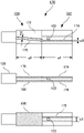
- FIG. 3 is a trihedral view (that is, a plan view, a side view and a bottom view from above) showing a specific example of the diamond magneto-optical sensor shown in FIG.
- FIG. 4 is a two-sided view (that is, a plan view and a front view from above) showing a state in which diamonds are arranged in a coplanar waveguide.
- FIG. 5 is a sectional view showing a magnetic field formed in diamond by microwave irradiation in the diamond magneto-optical sensor shown in FIG. FIG.
- FIG. 6 is a circuit diagram showing a diamond magneto-optical sensor according to a third embodiment of the present disclosure
- FIG. 7 is a circuit diagram showing a diamond magneto-optical sensor according to a fourth embodiment of the present disclosure
- FIG. 8 is a trihedral view (that is, a plan view, a side view and a bottom view from above) showing a specific example of the diamond magneto-optical sensor shown in FIG.
- FIG. 9 is a sectional view showing a magnetic field formed in diamond by microwave irradiation in the diamond magneto-optical sensor shown in FIG. FIG.
- FIG. 10 is a trihedral view (that is, a plan view, a side view, and a bottom view from above) showing a specific example of the diamond magneto-optical sensor according to the fifth embodiment of the present disclosure.
- FIG. 11 is a sectional view showing a magnetic field formed in diamond by microwave irradiation in the diamond magneto-optical sensor shown in FIG.
- FIG. 12 is a trihedral view (that is, plan view, side view and bottom view from above) showing a diamond magnetic sensor when microwave power is supplied by wireless transmission.
- FIG. 13 is a trihedral view (that is, a plan view, a side view and a bottom view from above) showing the diamond magneto-optical sensor according to the first modified example.
- FIG. 11 is a sectional view showing a magnetic field formed in diamond by microwave irradiation in the diamond magneto-optical sensor shown in FIG.
- FIG. 12 is a trihedral view (that is, plan view, side view and bottom view from
- FIG. 14 is a trihedral view (that is, a plan view, a side view and a bottom view from above) showing a diamond magneto-optical sensor according to the second modification.
- FIG. 15 is a schematic diagram showing a multistage ⁇ /4 transformer.
- FIG. 16 is a schematic diagram showing a tapered ⁇ /4 transformer.
- FIG. 17 is a schematic diagram showing the configuration of the measuring device used in the experiment.
- FIG. 18 is a plan view showing a microstripline resonator used in the experiment.
- FIG. 19 is a plan view showing a coplanar waveguide resonator used in the experiment.
- FIG. 20 is a graph showing changes in the intensity of fluorescence emitted from NV centers in diamond.
- FIG. 21 is a graph showing experimental results.
- Non-Patent Document 1 microwaves from a power supply were transmitted using a coplanar waveguide and irradiated to the NV center to cause magnetic resonance. It was necessary to supply microwaves with power. Also, when using a microstrip line, it is necessary to supply approximately the same microwave power.
- the microwave frequency for magnetic resonance of NV centers is about 3 GHz, and this frequency varies under the influence of magnetic field, electric field and temperature. Coefficients representing the extent of these effects (that is, changes in resonance frequency) are shown below. Effect of magnetic field: 28GHz/T Effect of electric field: 17 Hz/(V/cm) Effect of temperature: -74.2 kHz/K
- the transmission of excitation light, fluorescence, and microwaves should be performed remotely while securing insulation separation to avoid high-voltage dielectric breakdown. desirable.
- the transmission of excitation light and fluorescence can be performed remotely and with isolation by using optical fibers.
- microwave transmission it is difficult to secure insulation and separation in transmission using a coaxial cable, but if space transmission is performed by radio waves using a transmitting antenna and a receiving antenna, it is possible to remotely secure insulation and separation.
- spatially transmitting microwaves using a transmitting antenna and a receiving antenna it is desirable to achieve power saving, compactness, and low cost. That is, it is desirable to suppress the transmission power of microwaves, increase the antenna gain, and allow magnetic resonance to occur with microwaves of as low power as possible.
- an object of the present disclosure is to provide a diamond magneto-optical sensor that can operate with low-power microwaves.
- the diamond magneto-optical sensor includes a diamond having a color center with electron spins, a transmission circuit that transmits electromagnetic waves, and an irradiation that irradiates the diamond with the electromagnetic waves transmitted by the transmission circuit and the transmission circuit includes an impedance converter for lowering or increasing the impedance of the electromagnetic wave source that outputs the electromagnetic wave as viewed from the irradiation section. This allows the diamond magneto-optical sensor to operate with low power microwaves.
- a diamond magneto-optical sensor includes a diamond having a color center with electron spins, a transmission circuit that transmits electromagnetic waves, and an irradiation that irradiates the diamond with the electromagnetic waves transmitted by the transmission circuit and the irradiation section includes a resonator. This allows the diamond magneto-optical sensor to operate with low power microwaves.
- the transmission circuit can include an impedance converter for lowering or increasing the impedance of the electromagnetic wave source that outputs the electromagnetic waves as seen from the irradiation section.
- an impedance converter for lowering or increasing the impedance of the electromagnetic wave source that outputs the electromagnetic waves as seen from the irradiation section.
- the impedance converter may include a transformer. This makes it possible to easily form a diamond magneto-optical sensor.
- the impedance converter may include a ⁇ /4 transformer.
- the resonator may include a ⁇ /4 stub.
- the resonance frequency of the resonator can be adjusted with high accuracy, and the electromagnetic wave can be efficiently applied to the diamond.
- the ⁇ /4 stub may include a ⁇ /4 open stub. This makes it easier to design the shape of a diamond with high fluorescence collection efficiency. In addition, series resonance can be realized, short-circuit current can be increased, and microwaves with a stronger magnetic field can be irradiated.
- ⁇ /4 stubs may include ⁇ /4 short stubs.
- the ⁇ /4 stub may include two linear conductors arranged in parallel. As a result, the magnetic field applied to the diamond by microwaves can be increased.
- the ⁇ /4 stub may include four linear conductors arranged in parallel. As a result, the magnetic field applied to the diamond by microwaves can be increased.
- the ⁇ /4 stub may include two flat conductors, and the two flat conductors may be arranged in parallel facing each other.
- the thickness of the diamond may be greater than 0 and 0.3 mm or less, and the two linear conductors may sandwich the diamond and be spaced apart in the thickness direction of the diamond. .
- the magnetic field applied to the diamond by microwaves can be increased.
- the thickness of the diamond may be 0.5 mm or more and 3 mm or less, and the two flat conductors may sandwich the diamond and be spaced apart in the thickness direction of the diamond.
- the ⁇ /4 transformer may be formed in a tapered shape whose width continuously changes. Thereby, the impedance can be easily and accurately converted in a wide band.
- the ⁇ /4 transformer may be formed into a multi-stage type in which the width varies discretely. Thereby, the impedance can be easily and accurately converted in a wide band.
- the impedance converter may include a microstripline, and the width of the microstripline may be 1/2 or less of the length of the microstripline. As a result, impedance can be easily and accurately converted with little loss.
- the width of the ⁇ /4 stub may be 1/2 or less of the length of the ⁇ /4 stub. This allows resonance with less radiation.
- the center of the diamond may be located within a predetermined range from the connection end of the ⁇ /4 open stub with the transmission circuit, and the predetermined range is 1/8 or more of the electrical length of the ⁇ /4 open stub. /8 or less, and the length of the diamond along the longitudinal direction of the ⁇ /4 open stub may be 1/4 or less of the electrical length. As a result, the magnetic field applied to the diamond by microwaves can be increased.
- the center of the diamond may be located within a predetermined range from the shorted end of the ⁇ /4 short stub, and the predetermined range is 1/8 or more and 3/8 or less of the electrical length of the ⁇ /4 short stub.
- the length of the diamond along the longitudinal direction of the ⁇ /4 short stub may be 1/4 or less of the electrical length.
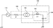
- a diamond magneto-optical sensor 100 according to the first embodiment of the present disclosure includes a diamond 102, a resonator 104, a transmission circuit 106 and a microwave source 110.
- FIG. This embodiment efficiently supplies microwaves to the diamond 102 by means of a resonator configured by a lumped constant circuit.
- Diamond 102 contains NV centers.
- the resonator 104 includes a coil L1 and a capacitor C1 and constitutes a series resonance circuit.
- the diamond 102 is arranged in the vicinity of the coil L1 (including the inside of the coil L1).
- the inside of the coil L1 means the space surrounded by the windings forming the coil L1.
- the resonator 104 is an irradiation unit for irradiating the diamond 102 with microwaves.
- Transmission circuit 106 includes an impedance transformer 108 and a coaxial cable of characteristic impedance Z1 connecting between impedance transformer 108 and microwave source 110 .
- the microwave source 110 is a power source that generates microwaves of a predetermined frequency.
- the characteristic impedance Z1 is, for example, 50 ⁇ , and the microwave source 110 supplies electromagnetic waves (ie, microwaves) to the diamond magneto-optical sensor 100 via the coaxial cable (ie, 50 ⁇ feeding).
- Impedance converter 108 is specifically a transformer. By using a transformer as the impedance converter 108, a diamond magneto-optical sensor can be easily formed. With this configuration, the resonator 104 and the impedance converter 108 function as resonators, and the magnetic field of microwaves from the microwave source 110 can be increased to irradiate the diamond 102 .
- the open-circuit voltage on the load side that is, the LC series resonator
- the impedance becomes N2 times
- the short-circuit current flowing through the series resonant circuit becomes 1/N times. Therefore, even if the power of the microwave output from the microwave source 110 is smaller than that of the conventional one, the diamond magneto-optical sensor 100 can function as a magnetic sensor if N is smaller than 1.
- a diamond magneto-optical sensor 120 according to the second embodiment of the present disclosure includes diamond 102, resonator 124, transmission circuit 126 and microwave source 110. As shown in FIG. This embodiment efficiently supplies microwaves to the diamond 102 by means of a resonator configured by a high frequency circuit.
- the resonator 124 includes a ⁇ /4 stub 122 and functions as a series resonant circuit. Diamond 102 is placed near ⁇ /4 stub 122 .
- the resonator 124 is an irradiation unit for irradiating the diamond 102 with microwaves.
- Transmission circuit 126 includes a ⁇ /4 transformer 128 and a coaxial cable of characteristic impedance Z 1 connecting between ⁇ /4 transformer 128 and microwave source 110 .
- the characteristic impedance Z1 is, for example, 50 ⁇ , and the microwave source 110 supplies microwaves to the diamond magneto-optical sensor 120 via a coaxial cable.
- a ⁇ /4 transformer 128 functions as an impedance converter.
- the ⁇ /4 stub 122 is, for example, a ⁇ /4 open stub.
- the impedance can be accurately converted between the transmission circuit 126 (specifically, the coaxial cable with the characteristic impedance Z1) and the resonator 124, and the electromagnetic wave can be efficiently converted into the diamond 102. Irradiation is possible.
- the ⁇ /4 stub 122 and the ⁇ /4 transformer 128 function as resonators to increase the magnetic field of the microwaves from the microwave source 110 and irradiate the diamond 102 with them. Therefore, the diamond magneto-optical sensor 120 can function as a magnetic sensor even if the power of the microwave output from the microwave source 110 is smaller than that of the conventional one.
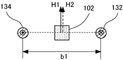
- ⁇ /4 stub 122 is composed of two copper wires 132 and 134 .
- the two copper wires 132 and 134 are ⁇ /4 open stubs.
- Each of the copper wires 132 and 134 has a diameter d of 0.45 mm, a length a1 of ⁇ /4 for microwaves of about 3 GHz (also considering the surrounding dielectric), 20 mm.
- a distance b1 between the copper wires 132 and 134 is 4 mm.
- Diamond 102 is positioned between copper lines 132 and 134 .
- Each of the copper wires 132 and 134 may have a diameter of about 50 ⁇ m or more and 2 mm or less.
- the diamond 102 preferably has a thickness of 1 ⁇ m or more and 0.3 mm or less.
- the ⁇ /4 transformer 128 is composed of a dielectric substrate 140 , a copper foil 130 arranged on the surface of the dielectric substrate 140 , and a copper foil 138 arranged on the back surface of the dielectric substrate 140 .
- the dielectric substrate 140 is made of glass epoxy, for example.
- Copper foil 130 is connected to copper wire 132 .
- the copper foil 130 is composed of a first portion with a width w1 of 3 mm and a second portion with a width w2 of 10 mm. The length a2 of the second portion is 20 mm.
- Receptacle 136 is an SMA-type receptacle into which a coaxial cable plug is attached.
- the centerline (or signal line) of receptacle 136 is connected to copper foil 130 and the ground of receptacle 136 is connected to copper foil 138 .
- Copper foil 138 is connected to copper wire 134 .
- the impedance of the ⁇ /4 stub 122 which is a ⁇ /4 open stub, is 300 ⁇ , for example.
- ⁇ /4 stub 122 To increase the magnetic field applied to diamond 102 by microwaves at the junction of ⁇ /4 transformer 128 and ⁇ /4 stub 122 with ⁇ /4 transformer 128 having an impedance of 25 ⁇ , ⁇ /4 stub 122 It is preferable to adjust the position of the placed diamond 102 .
- the distance e1 from the connection end of the ⁇ /4 stub 122 with the transmission circuit 126 (specifically, the ⁇ /4 transformer 128) to the center of the diamond 102 is the ⁇ /4 stub 122 (that is, the ⁇ /4 open stub) is preferably 1/4 of the electrical length of .
- the distance e1 may be in the range of (1/4) ⁇ (1/8) of the electrical length of the ⁇ /4 stub 122 (that is, the range of 1/8 or more and 3/8 or less).
- the thickness of the diamond 102 in the direction of the interval b1 is preferably greater than 0 and 0.3 mm or less.
- the length along the longitudinal direction of the ⁇ /4 stub 122 (that is, the ⁇ /4 open stub) of the diamond 102 is preferably 1/4 or less of the electrical length of the ⁇ /4 stub 122 .
- the magnetic fields formed inside the diamond 102 are magnetic fields H1 and H2 indicated by solid line arrows due to an upward current perpendicular to the paper surface, and magnetic fields H3 and H4 indicated by broken line arrows due to a downward current perpendicular to the paper surface. is formed. Since these fields almost cancel each other, the resultant field is small. On the other hand, referring to FIG. 5, in the configuration shown in FIG. Since the magnetic field H1 and the magnetic field H2 indicated by the dashed arrow are directed in the same direction, they increase.
- the diamond magneto-optical sensor 120 can function as a magnetic sensor even if the power of the microwave output from the microwave source 110 is smaller than that of the conventional one.
- a diamond magneto-optical sensor 142 according to the third embodiment of the present disclosure includes diamond 102, resonator 144, transmission circuit 146 and microwave source 110. As shown in FIG. This embodiment efficiently supplies microwaves to the diamond 102 by means of a resonator configured by a lumped constant circuit.
- the resonator 144 includes a coil L2 and a capacitor C2 and constitutes a parallel resonance circuit.
- the diamond 102 is arranged in the vicinity of the coil L2 (including the inside of the coil L2).
- the resonator 144 is an irradiation unit for irradiating the diamond 102 with microwaves.
- Transmission circuit 146 includes an impedance transformer 148 and a coaxial cable of characteristic impedance Z1 connecting between impedance transformer 148 and microwave source 110 .
- Characteristic impedance Z1 is, for example, 50 ⁇ , and microwave source 110 supplies microwaves to diamond magneto-optical sensor 142 via a coaxial cable.
- Impedance converter 148 is specifically a transformer.
- a diamond magneto-optical sensor By using a transformer for the impedance converter 148, a diamond magneto-optical sensor can be easily formed. With this configuration, the resonator 144 and the impedance converter 148 function as resonators, and the microwaves from the microwave source 110 can be increased to irradiate the diamond 102 .
- the diamond magneto-optical sensor 142 can function as a magnetic sensor even if the power of the microwave output from the microwave source 110 is smaller than that of the conventional one.
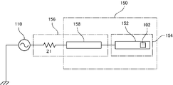
- a diamond magneto-optical sensor 150 according to the fourth embodiment of the present disclosure includes diamond 102, resonator 154, transmission circuit 156 and microwave source 110. As shown in FIG. This embodiment efficiently supplies microwaves to the diamond 102 by means of a resonator configured by a high frequency circuit.
- the resonator 154 includes a ⁇ /4 stub 152 and functions as a parallel resonant circuit. Diamond 102 is placed near ⁇ /4 stub 152 .
- the resonator 154 is an irradiation unit for irradiating the diamond 102 with microwaves.
- Transmission circuit 156 includes a ⁇ /4 transformer 158 and a coaxial cable of characteristic impedance Z 1 connecting between ⁇ /4 transformer 158 and microwave source 110 .
- the characteristic impedance Z1 is, for example, 50 ⁇ , and the microwave source 110 supplies microwaves to the diamond magneto-optical sensor 150 via a coaxial cable.
- a ⁇ /4 transformer 158 functions as an impedance converter.
- the ⁇ /4 stub 152 is, for example, a ⁇ /4 short stub.
- the impedance can be accurately converted between the transmission circuit 156 (specifically, the coaxial cable with the characteristic impedance Z1) and the resonator 154, and the electromagnetic wave can be efficiently converted into the diamond 102. Irradiation is possible.
- the ⁇ /4 stub 152 and the ⁇ /4 transformer 158 function as resonators to increase the magnetic field of microwaves from the microwave source 110 and irradiate the diamond 102 with them. Therefore, the diamond magneto-optical sensor 150 can function as a magnetic sensor even if the power of the microwave output from the microwave source 110 is smaller than that of the conventional one.
- the ⁇ /4 stub 152 is composed of a flat copper foil 164 .
- the copper foil 164 is formed by bending into a rectangle with one side removed so that the width w4 is 4 mm and the length a3 is 20 mm. That is, the copper foil 164 has a configuration in which two ⁇ /4 stubs are short-circuited at the bent portion of the copper foil 164 (the bent portion is hereinafter referred to as the short-circuit end).
- ⁇ /4 stub 152 is a ⁇ /4 short stub.
- the width w4 of the ⁇ /4 stub 152 is not limited to the above values.
- the width w4 of the ⁇ /4 stub 152 should be half or less of the length a3 of the ⁇ /4 stub 152. This allows resonance with less radiation.
- a ⁇ /4 transformer 158 is composed of two parallel copper wires 160 and 162 connected to a copper foil 164 .
- the copper wires 160 and 162 have a length a4 of 20 mm and a spacing b2 of 4 mm.
- Receptacle 136 is an SMA-type receptacle into which a coaxial cable plug is attached.
- the centerline (or signal line) of receptacle 136 is connected to copper wire 160 and the ground of receptacle 136 is connected to copper wire 162 .
- the diamond 102 is arranged within the space surrounded by the copper foil 164 (ie inside the copper foil 164).
- the impedance of the ⁇ /4 stub 152 which is a ⁇ /4 short stub, is 100 ⁇ , for example.
- ⁇ /4 transformer 158 having an impedance of 300 ⁇ and increase the magnetic field applied to diamond 102 by microwaves at the junction of ⁇ /4 transformer 158 and ⁇ /4 stub 152, ⁇ It is preferable to adjust the position of the diamond 102 placed on the /4 stub 152 .
- the distance e2 from the shorted end of the ⁇ /4 stub 152 to the center of the diamond 102 is preferably 1/4 of the electrical length of the ⁇ /4 stub 152 (that is, the ⁇ /4 short stub).
- the distance e2 may be in the range of (1/4) ⁇ (1/8) of the electrical length of the ⁇ /4 stub 152 (that is, the range of 1/8 or more and 3/8 or less).
- the thickness of the diamond 102 in the direction perpendicular to the ⁇ /4 stub 152 (that is, the two parallel flat plate portions) is preferably 0.5 mm or more and 3 mm or less.
- the length along the longitudinal direction of the ⁇ /4 stub 152 (that is, the ⁇ /4 short stub) of the diamond 102 is preferably 1/4 or less of the electrical length of the ⁇ /4 stub 152 .
- the magnetic fields H1 and H3 indicated by the solid line arrows and the magnetic fields H2 and H4 indicated by the broken line arrows are directed in the same direction (that is, upward in FIG. 9). so it increases.
- the current distribution of the copper foil 164 is symmetrical in both the left-right direction and the up-down direction. Magnetic field uniformity is increased.
- a diamond magneto-optical sensor 300 is composed of a diamond 102, a ⁇ /4 stub 302, a ⁇ /4 transformer 304 and a receptacle 136.
- the ⁇ /4 stub 302 is composed of four copper wires 310.
- Four copper wires 310 constitute a ⁇ /4 open stub.
- Each of the copper wires 310 has a diameter d of 0.45 mm and a length a8 of about 20 mm, which is ⁇ /4 for microwaves of about 3 GHz.
- a distance g between the copper wires 310 is 2 mm.
- Diamond 102 is placed in the center of four copper wires 310 .
- the ⁇ /4 stub 302 is composed of a flexible substrate 306, a copper foil 308 arranged on the front surface of the flexible substrate 306, and a copper foil 312 arranged on the back surface of the flexible substrate 306.
- the copper foil 308 has a width w8 of 1 mm and a length a9 of about 15 mm.
- the centerline (or signal line) of receptacle 136 is connected to copper foil 308 and the ground of receptacle 136 is connected to copper foil 312 .
- the impedance of the ⁇ /4 stub 302, which is a ⁇ /4 open stub, is, for example, 200 ⁇
- the impedance of the ⁇ /4 transformer 304 is, for example, 20 ⁇ .
- the diamond 102 placed on the ⁇ /4 stub 302 is is preferably adjusted.
- the magnetic fields H5 and H8 are oriented in the same direction, that is, in the upper right direction in FIG. 11, and the magnetic fields are strengthened mutually.
- the magnetic fields H6 and H7 are oriented in the same direction, that is, in the diagonally downward right direction in FIG. 11, and the magnetic fields are mutually strengthened.
- a composite magnetic field directed to the right is formed by the magnetic fields H5 to H8. That is, a magnetic field can be applied in a direction parallel to the surface of flexible substrate 306 .
- a magnetic field can be formed in the direction perpendicular to the substrate (see FIGS. 5 and 9).
- the direction of the microwave magnetic field with respect to the substrate may be vertical or horizontal. There are times when it is preferable. If the vertical orientation is preferred, the configurations shown in Figures 3 or 8, for example, can be used. If a horizontal orientation is preferred, the configuration shown in FIG. 10, for example, can be used.
- the microwave power may be supplied by wire or by wireless transmission in space.
- the connection of the SMA receptacle to the transmission circuit has been shown.
- a transmission circuit that receives microwaves with a monopole antenna and supplies power to the resonator side that is directly connected to the monopole antenna can be used.
- diamond magneto-optical sensor 330 comprises diamond 102 , ⁇ /4 stub 332 , ⁇ /4 transformer 334 and monopole antenna 336 .
- the ⁇ /4 stub 332 is composed of a linear conductor 342 (eg, copper wire) and a portion of a linear conductor 338 (eg, copper wire) (that is, a portion corresponding to the linear conductor 342).
- ⁇ /4 stub 332 is a ⁇ /4 open stub.
- the ⁇ /4 transformer 334 is composed of a flexible substrate 340, a copper foil 344, and a portion of the linear conductor 338 (that is, the portion facing the copper foil 344).
- the characteristic impedance of monopole antenna 336 is, for example, 37 ⁇
- the characteristic impedances of ⁇ /4 transformer 334 and ⁇ /4 stub 332 are, for example, 20 ⁇ and 200 ⁇ , respectively. That is, microwaves are received by the monopole antenna 336, converted to low impedance, and series-resonated by the ⁇ /4 open stub.
- a diamond magneto-optical sensor according to the first modification uses a flexible substrate.
- a diamond magneto-optical sensor 170 according to the first modification differs from the diamond magneto-optical sensor 120 shown in FIG.
- the ⁇ /4 stub 122 is composed of a flexible substrate 172 , a copper foil 174 arranged on the front surface of the flexible substrate 172 , and a copper foil 178 arranged on the rear surface of the flexible substrate 172 .
- the flexible substrate 172 is made of film-like polyimide.
- Each of the copper foils 174 and 178 has a width w5 of 0.5 mm, a length a5 of 20 mm, and a distance b3 therebetween of 4 mm. Copper foil 174 and copper foil 178 are ⁇ /4 open stubs.
- ⁇ /4 transformer 128 includes flexible substrate 172 , copper foil 176 located on the front side of flexible substrate 172 and connected to copper foil 174 , and copper foil 176 located on the back side of flexible substrate 172 and connected to copper foil 178 . and copper foil 180 .
- the width w6 of the copper foil 176 is 1 mm, and the length a6 of the copper foil 176 is 15 mm.
- Flexible substrate 172 constitutes both ⁇ /4 stub 122 and ⁇ /4 transformer 128, so its length (ie, a5+a6) is 35 mm.
- the center line (or signal line) of receptacle 136 which is an SMA type receptacle into which a coaxial cable plug is attached, is connected to copper foil 176 and the ground of receptacle 136 is connected to copper foil 180.
- FIG. Diamond 102 is placed in the space between copper foils 174 and 178 where flexible substrate 172 has been cut away.
- the characteristic impedance of receptacle 136 is 50 ⁇ .
- the characteristic impedances of ⁇ /4 transformer 128 and ⁇ /4 stub 122 are 20 ⁇ and 200 ⁇ , respectively.
- the diamond magneto-optical sensor 170 functions as a series resonance circuit, similar to the configuration shown in FIG. 5, the diamond magneto-optical sensor 170 can increase the intensity of the magnetic field formed inside the diamond 102 more than the conventional one (see FIG. 4). Therefore, the diamond magneto-optical sensor 170 can function as a magnetic sensor even if the power of the microwave output from the microwave source 110 is smaller than that of the conventional one.
- a diamond magneto-optical sensor 182 differs from the diamond magneto-optical sensor 170 shown in FIG. ⁇ /4 stub 122 is constructed from copper foils 184 and 186 .
- Each of the copper foils 184 and 186 has a width w7 of 4 mm, a length a7 of 20 mm, and a distance b4 between them of 4 mm.
- Copper foils 184 and 186 are ⁇ /4 open stubs.
- Diamond 102 is positioned between copper foils 184 and 186 .
- the characteristic impedance of receptacle 136 is 50 ⁇ .
- the characteristic impedances of ⁇ /4 transformer 128 and ⁇ /4 stub 122 are 20 ⁇ and 200 ⁇ , respectively.
- the diamond magneto-optical sensor 182 functions as a series resonant circuit, similar to the configuration shown in FIG. 5, the diamond magneto-optical sensor 182 can increase the intensity of the magnetic field formed inside the diamond 102 more than the conventional one (see FIG. 4). Therefore, the diamond magneto-optical sensor 182 can function as a magnetic sensor even if the power of the microwave output from the microwave source 110 is smaller than that of the conventional one.
- the ⁇ /4 transformer 128 is formed of a ⁇ /4 stub (that is, copper foil) with a predetermined width w2
- a ⁇ /4 transformer in which the width w changes stepwise as shown in FIG.
- the diamond magneto-optical sensor constructed by using these in the ⁇ /4 transformer 128 shown in FIG. can function as
- the impedance converter is a transformer or a ⁇ /4 transformer, it is not limited to this.
- a microstrip line may be used for the impedance converter.
- the width of the microstripline is preferably less than half the length of the microstripline.
- a diamond magneto-optical sensor having a color center with electron spin may be used.
- a color center having an electron spin is a center that forms a spin triplet state and emits light when excited, and NV centers are typical examples.
- silicon-vacancy centers (ie Si-V centers), germanium-vacancy centers (ie Ge-V centers), and tin-vacancy centers (ie Sn-V centers) also have color with electron spin. Centers are known to exist. Therefore, a diamond magneto-optical sensor may be constructed by using diamond containing these instead of diamond containing NV centers.
- the configuration (i.e., irradiation system) for irradiating the diamond 210 included in the diamond magneto-optical sensor 216 with the excitation light in the measurement apparatus includes a light source 200, a collimating lens 202, a dichroic mirror 204, a sphere Includes lens 206 and optical fiber 208 .
- a configuration for observing fluorescence emitted from the diamond 210 includes an optical fiber 208 , a ball lens 206 , a dichroic mirror 204 , an LPF (Long Pass Filter) 212 and a photodetector 214 .
- a configuration i.e., a microwave system
- for irradiating the diamond 210 with microwaves includes a microwave source (not shown) and a coaxial cable 220. is shared by the resonators that make up the
- An LD (laser diode) element (specifically, L515A1 manufactured by Thorlabs) was used as the light source 200 for generating excitation light to generate 5 mW green laser light (that is, excitation light).
- the excitation light output from the light source 200 was condensed by the collimator lens 202 and then made incident on the dichroic mirror 204 .
- the collimating lens 202 is LA1116-A manufactured by Thorlabs
- the dichroic mirror 204 is S06-RG manufactured by Suruga Seiki Co., Ltd.
- the excitation light (that is, green light) incident on the dichroic mirror 204 is reflected by the dichroic mirror 204 .
- the reflected light was condensed by a ball lens 206 , entered into an optical fiber 208 (specifically, a core), transmitted through the optical fiber 208 , and irradiated onto a diamond 210 .
- an optical fiber 208 specifically, a core
- MS-08-4.35P1 diameter 8 mm
- An optical digital cable with a core diameter of ⁇ 0.9 mm was used as the optical fiber 208 .
- the fluorescence incident on the optical fiber 208 was propagated through the optical fiber 208 , converted into parallel light by the ball lens 206 , and made incident on the dichroic mirror 204 .
- the fluorescence (that is, red light) that has entered the dichroic mirror 204 is transmitted through the dichroic mirror 204 and enters the LPF 212 .
- Fluorescence that passed through LPF 212 was detected by photodetector 214 .
- the LPF 212 passes light of wavelengths equal to or greater than a predetermined wavelength, and cuts (for example, reflects) light of wavelengths smaller than a predetermined wavelength.
- LOPF-25C-593 manufactured by Opto Sigma was used.
- a photodiode (specifically, S6967 manufactured by Hamamatsu Photonics K.K.) was used for the photodetector 214 .
- Diamond's emission light is red light and passes through the LPF 212 , whereas the excitation light has a shorter wavelength and does not pass through the LPF 212 . This prevents the excitation light emitted from the light source 200 from being detected by the photodetector 214 and becoming noise, thereby reducing the detection sensitivity.
- FIG. 18 a microstripline resonator having the configuration and dimensions shown in FIG. 18 and a coplanar waveguide resonator having the configuration and dimensions shown in FIG. 19 were used.
- a conductor functioning as a ground is arranged on the entire back surface of the dielectric substrate on which the microstrip lines are arranged.
- cubic diamonds which will be described later, are placed at the positions shown in FIGS. 18 and 19 .
- a plug of coaxial cable 220 (not shown in FIG.
- type Ib diamond is used, and electrons are injected into it with an electron beam acceleration energy of 3 MeV and an electron beam dose of 3 ⁇ 10 18 /cm 2 , and then at 800° C. for about 1 hour. Annealed to produce a diamond containing NV centers. This was cut into a cube with one side of 1 mm to prepare a diamond 210 used for measurement.
- a microwave (1 W) generated by a microwave generator (not shown) was transmitted to the diamond magneto-optical sensor 216 using a coaxial cable 220.
- a coaxial cable with a characteristic impedance of 50 ⁇ was used for the coaxial cable 220 .
- the power of the microwave supplied to the coaxial cable 220 was varied in the range of -16 dBm to 30 dBm.
- the frequency of the microwave was varied in the range of 2.74 GHz to 2.94 GHz.
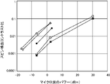
- the spin detection contrast ratio (that is, the value obtained by dividing the size S of the valley in the graph by the fluorescence intensity S0), which is the rate of decrease in red light luminance, can be calculated.
- the following formula 1 is known as a theoretical formula for the sensitivity ⁇ B (that is, the resolution of the detected magnetic field B) of the diamond magneto-optical sensor, and the spin detection contrast ratio affects the sensitivity ⁇ B.
- Equation 1 ⁇ is the gyromagnetic ratio (ie, constant) and is close to the gyromagnetic ratio of electrons (ie, 1.76 ⁇ 10 11 rad/s/T).
- ⁇ is the fluorescence detection efficiency and C is the spin detection contrast.
- N is the number of negatively charged NV centers present in the area where the excitation light is applied and the fluorescence is collected.
- T2 is the transverse relaxation time of the electron spin. From the above theoretical expression of sensitivity (Equation 1), the higher the spin detection contrast, the smaller the sensitivity ⁇ B and the higher the sensitivity.
- the troughs in fluorescence intensity i.e., red light intensity
- the white circles are the result of using the ⁇ /4 open stub resonator shown in FIG.
- the black circles are the results using the ⁇ /4 short stub resonator shown in FIG.
- the open triangles are the results using the ⁇ /4 open stub resonator shown in FIG.
- the white squares are the results using the microstripline resonator shown in FIG.
- the black squares are the results using the coplanar waveguide resonator shown in FIG.
- Example 1 Using the configuration of the second embodiment (see FIG. 3), changing the diameter of the copper wires 132 and 134 constituting the ⁇ /4 stub and the size of the diamond, the above Example 1 (see FIG. 17) The experiment was conducted in the same way as Specifically, copper wires with diameters of 0.1 mm, 0.3 mm, 1.0 mm and 1.5 mm were used as the copper wires 132 and 134 . As comparative examples, copper wires with diameters of 0.02 mm and 3 mm were used as the copper wires 132 and 134 . The diamonds 210 (see FIG. 17) with thicknesses of 0.8 ⁇ m, 10 ⁇ m, 0.1 mm, 0.3 mm and 0.5 mm were used.
Landscapes
- Physics & Mathematics (AREA)
- Condensed Matter Physics & Semiconductors (AREA)
- General Physics & Mathematics (AREA)
- Engineering & Computer Science (AREA)
- Power Engineering (AREA)
- Measuring Magnetic Variables (AREA)
Abstract
Description
非特許文献1に倣い、コプレーナ導波路を用いて電源からのマイクロ波を伝送してNVセンタに照射し、磁気共鳴させたところ、十分に磁気共鳴させるためには、約30dBm(=1W)のパワーでマイクロ波を供給する必要があった。また、マイクロストリップラインを用いた場合にも、ほぼ同程度のマイクロ波パワーを供給する必要があった。
磁界の影響:28GHz/T
電界の影響:17Hz/(V/cm)
温度の影響:-74.2kHz/K
本開示によれば、小さい電力のマイクロ波により動作可能なダイヤモンド光磁気センサを提供できる。
本開示の実施形態の内容を列記して説明する。以下に記載する実施形態の少なくとも一部を任意に組み合わせてもよい。
以下の実施形態においては、同一の部品には同一の参照番号を付してある。それらの名称及び機能も同一である。したがって、それらについての詳細な説明は繰返さない。
図1を参照して本開示の第1実施形態に係るダイヤモンド光磁気センサ100は、ダイヤモンド102、共振器104、伝送回路106及びマイクロ波源110を含む。本実施形態は、集中定数回路により構成した共鳴器により、ダイヤモンド102にマイクロ波を効率的に供給する。ダイヤモンド102はNVセンタを含む。
図2を参照して本開示の第2実施形態に係るダイヤモンド光磁気センサ120は、ダイヤモンド102、共振器124、伝送回路126及びマイクロ波源110を含む。本実施形態は、高周波回路により構成した共鳴器により、ダイヤモンド102にマイクロ波を効率的に供給する。
上記では、直列共振により、ダイヤモンド102に照射するマイクロ波を増大する場合を説明したが、これに限定されない。第3実施形態においては、並列共振によりダイヤモンド102に照射するマイクロ波を増大する。図6を参照して本開示の第3実施形態に係るダイヤモンド光磁気センサ142は、ダイヤモンド102、共振器144、伝送回路146及びマイクロ波源110を含む。本実施形態は、集中定数回路により構成した共鳴器により、ダイヤモンド102にマイクロ波を効率的に供給する。
図7を参照して本開示の第4実施形態に係るダイヤモンド光磁気センサ150は、ダイヤモンド102、共振器154、伝送回路156及びマイクロ波源110を含む。本実施形態は、高周波回路により構成した共鳴器により、ダイヤモンド102にマイクロ波を効率的に供給する。
上記では、第2実施形態として、ガラスエポキシ等の誘電体基板を用い、2本の銅線によりλ/4スタブを構成する場合を説明した。それに対して、第5実施形態においては、フレキシブル基板を用い、4本の銅線によりλ/4スタブを構成する。図10を参照して、本開示の第5実施形態に係るダイヤモンド光磁気センサ300は、ダイヤモンド102、λ/4スタブ302、λ/4変成器304及びレセプタクル136により構成されている。
上記では、第2実施形態として、誘電体基板(例えば、ガラスエポキシ)を用いる場合を説明したが、これに限定されない。第1変形例に係るダイヤモンド光磁気センサは、フレキシブル基板を用いる。
上記した第1変形例では、λ/4スタブ122として線状の銅箔を用いる場合を説明したが、これに限定されない。第2変形例に係るダイヤモンド光磁気センサは、λ/4スタブ122として平面状の銅箔を用いる。

102、210 ダイヤモンド
104、124、144、154 共振器
106、126、146、156 伝送回路
108、148 インピーダンス変換器
110 マイクロ波源
122、152、302、332 λ/4スタブ
128、158、304、334 λ/4変成器
130、138、164、174、176、178、180、184、186、308、312、344 銅箔
132、134、160、162、310 銅線
136 レセプタクル
140 誘電体基板
172、188、306、340 フレキシブル基板
200 光源
202 コリメートレンズ
204 ダイクロイックミラー
206 球レンズ
208 光ファイバ
212 LPF
214 光検出器
220 同軸ケーブル
336 モノポールアンテナ
338、342 線状導体
900、902、904 導電体
a1、a2、a3、a4、a5、a6、a7、a8、a9 長さ
b1、b2、b3、b4、g 間隔
C1、C2 キャパシタ
d、d1 直径
e1、e2 距離
H1、H2、H3、H4、H5、H6、H7、H8 磁界
L1、L2 コイル
w1、w2、w4、w5、w6、w7、w8 幅
Z1 インピーダンス
Claims (19)
- 電子スピンを持つカラーセンタを有するダイヤモンドと、
電磁波を伝送する伝送回路と、
前記伝送回路により伝送される前記電磁波を前記ダイヤモンドに照射する照射部とを含み、
前記伝送回路は、前記電磁波を出力する電磁波源のインピーダンスを前記照射部から見て低く又は高くするためのインピーダンス変換器を含む、ダイヤモンド光磁気センサ。 - 電子スピンを持つカラーセンタを有するダイヤモンドと、
電磁波を伝送する伝送回路と、
前記伝送回路により伝送される前記電磁波を前記ダイヤモンドに照射する照射部とを含み、
前記照射部は、共振器を含む、ダイヤモンド光磁気センサ。 - 前記伝送回路は、前記電磁波を出力する電磁波源のインピーダンスを前記照射部から見て低く又は高くするためのインピーダンス変換器を含む、請求項2に記載のダイヤモンド光磁気センサ。
- 前記インピーダンス変換器は、変圧器を含む、請求項1又は請求項3に記載のダイヤモンド光磁気センサ。
- 前記インピーダンス変換器は、λ/4変成器を含む、請求項1又は請求項3に記載のダイヤモンド光磁気センサ。
- 前記共振器は、λ/4スタブを含む、請求項2又は請求項3に記載のダイヤモンド光磁気センサ。
- 前記λ/4スタブは、λ/4オープンスタブを含む、請求項6に記載のダイヤモンド光磁気センサ。
- 前記λ/4スタブは、λ/4ショートスタブを含む、請求項6に記載のダイヤモンド光磁気センサ。
- 前記λ/4スタブは、平行に配置された2つの線状の導電体を含む、請求項6に記載のダイヤモンド光磁気センサ。
- 前記λ/4スタブは、平行に配置された4つの線状の導電体を含む、請求項6に記載のダイヤモンド光磁気センサ。
- 前記λ/4スタブは、2つの平板状の導電体を含み、
前記2つの平板状の導電体は、相互に対向して平行に配置される、請求項6に記載のダイヤモンド光磁気センサ。 - 前記ダイヤモンドの厚さは、0より大きく0.3mm以下であり、
前記2つの線状の導電体は、前記ダイヤモンドを挟み、前記ダイヤモンドの前記厚さ方向に離隔して配置される、請求項9に記載のダイヤモンド光磁気センサ。 - 前記ダイヤモンドの厚さは、0.5mm以上3mm以下であり、
前記2つの平板状の導電体は、前記ダイヤモンドを挟み、前記ダイヤモンドの前記厚さ方向に離隔して配置される、請求項11に記載のダイヤモンド光磁気センサ。 - 前記λ/4変成器は、幅が連続的に変化するテーパ状に形成される、請求項5に記載のダイヤモンド光磁気センサ。
- 前記λ/4変成器は、幅が離散的に変化する多段型に形成される、請求項5に記載のダイヤモンド光磁気センサ。
- 前記インピーダンス変換器は、マイクロストリップラインを含み、
前記マイクロストリップラインの幅は、前記マイクロストリップラインの長さの1/2以下である、請求項5に記載のダイヤモンド光磁気センサ。 - 前記λ/4スタブの幅は、前記λ/4スタブの長さの1/2以下である、請求項6に記載のダイヤモンド光磁気センサ。
- 前記ダイヤモンドの中心は、前記λ/4オープンスタブの前記伝送回路との接続端から所定範囲内に位置し、
前記所定範囲は、前記λ/4オープンスタブの電気長の1/8以上3/8以下であり、
前記ダイヤモンドの、前記λ/4オープンスタブの長手方向に沿った長さは、前記電気長の1/4以下である、請求項7に記載のダイヤモンド光磁気センサ。 - 前記ダイヤモンドの中心は、前記λ/4ショートスタブの短絡端から所定範囲内に位置し、
前記所定範囲は、前記λ/4ショートスタブの電気長の1/8以上3/8以下であり、
前記ダイヤモンドの、前記λ/4ショートスタブの長手方向に沿った長さは、前記電気長の1/4以下である、請求項8に記載のダイヤモンド光磁気センサ。
Priority Applications (4)
| Application Number | Priority Date | Filing Date | Title |
|---|---|---|---|
| JP2023511369A JPWO2022210696A1 (ja) | 2021-03-31 | 2022-03-29 | |
| EP22780907.6A EP4318012A1 (en) | 2021-03-31 | 2022-03-29 | Diamond magneto-optical sensor |
| CN202280025980.3A CN117099008A (zh) | 2021-03-31 | 2022-03-29 | 金刚石光磁传感器 |
| US18/283,940 US20240168107A1 (en) | 2021-03-31 | 2022-03-29 | Diamond magneto-optical sensor |
Applications Claiming Priority (2)
| Application Number | Priority Date | Filing Date | Title |
|---|---|---|---|
| JP2021-059796 | 2021-03-31 | ||
| JP2021059796 | 2021-03-31 |
Publications (1)
| Publication Number | Publication Date |
|---|---|
| WO2022210696A1 true WO2022210696A1 (ja) | 2022-10-06 |
Family
ID=83459437
Family Applications (1)
| Application Number | Title | Priority Date | Filing Date |
|---|---|---|---|
| PCT/JP2022/015394 WO2022210696A1 (ja) | 2021-03-31 | 2022-03-29 | ダイヤモンド光磁気センサ |
Country Status (5)
| Country | Link |
|---|---|
| US (1) | US20240168107A1 (ja) |
| EP (1) | EP4318012A1 (ja) |
| JP (1) | JPWO2022210696A1 (ja) |
| CN (1) | CN117099008A (ja) |
| WO (1) | WO2022210696A1 (ja) |
Cited By (1)
| Publication number | Priority date | Publication date | Assignee | Title |
|---|---|---|---|---|
| WO2024080386A1 (ja) * | 2022-10-13 | 2024-04-18 | スミダコーポレーション株式会社 | 磁場測定装置 |
Citations (10)
| Publication number | Priority date | Publication date | Assignee | Title |
|---|---|---|---|---|
| JPS5254349A (en) * | 1975-10-29 | 1977-05-02 | Dainichi Nippon Cables Ltd | Coupler for waveguide line |
| US4760400A (en) * | 1986-07-15 | 1988-07-26 | Canadian Marconi Company | Sandwich-wire antenna |
| JP2000114870A (ja) * | 1998-10-06 | 2000-04-21 | Nec Corp | マイクロ波発振器 |
| JP2000124713A (ja) * | 1998-10-12 | 2000-04-28 | Nec Corp | マイクロ波共振回路及びマイクロ波発振器 |
| JP2004163859A (ja) * | 2002-09-17 | 2004-06-10 | Sumitomo Osaka Cement Co Ltd | 光変調器 |
| WO2009107681A1 (ja) * | 2008-02-25 | 2009-09-03 | 国立大学法人京都大学 | マイクロ波を用いた不純物ドープ金属酸化物の製造方法 |
| US20180275209A1 (en) * | 2017-03-24 | 2018-09-27 | Lockheed Martin Corporation | Standing-wave radio frequency exciter |
| JP2019053025A (ja) * | 2017-09-12 | 2019-04-04 | スミダコーポレーション株式会社 | 高周波磁場発生装置 |
| JP2020134415A (ja) * | 2019-02-22 | 2020-08-31 | スミダコーポレーション株式会社 | 測定装置 |
| JP2021059796A (ja) | 2019-10-04 | 2021-04-15 | 株式会社キノクニエンタープライズ | 液体循環式冷却胴着構造 |
-
2022
- 2022-03-29 EP EP22780907.6A patent/EP4318012A1/en active Pending
- 2022-03-29 CN CN202280025980.3A patent/CN117099008A/zh active Pending
- 2022-03-29 JP JP2023511369A patent/JPWO2022210696A1/ja active Pending
- 2022-03-29 US US18/283,940 patent/US20240168107A1/en active Pending
- 2022-03-29 WO PCT/JP2022/015394 patent/WO2022210696A1/ja active Application Filing
Patent Citations (10)
| Publication number | Priority date | Publication date | Assignee | Title |
|---|---|---|---|---|
| JPS5254349A (en) * | 1975-10-29 | 1977-05-02 | Dainichi Nippon Cables Ltd | Coupler for waveguide line |
| US4760400A (en) * | 1986-07-15 | 1988-07-26 | Canadian Marconi Company | Sandwich-wire antenna |
| JP2000114870A (ja) * | 1998-10-06 | 2000-04-21 | Nec Corp | マイクロ波発振器 |
| JP2000124713A (ja) * | 1998-10-12 | 2000-04-28 | Nec Corp | マイクロ波共振回路及びマイクロ波発振器 |
| JP2004163859A (ja) * | 2002-09-17 | 2004-06-10 | Sumitomo Osaka Cement Co Ltd | 光変調器 |
| WO2009107681A1 (ja) * | 2008-02-25 | 2009-09-03 | 国立大学法人京都大学 | マイクロ波を用いた不純物ドープ金属酸化物の製造方法 |
| US20180275209A1 (en) * | 2017-03-24 | 2018-09-27 | Lockheed Martin Corporation | Standing-wave radio frequency exciter |
| JP2019053025A (ja) * | 2017-09-12 | 2019-04-04 | スミダコーポレーション株式会社 | 高周波磁場発生装置 |
| JP2020134415A (ja) * | 2019-02-22 | 2020-08-31 | スミダコーポレーション株式会社 | 測定装置 |
| JP2021059796A (ja) | 2019-10-04 | 2021-04-15 | 株式会社キノクニエンタープライズ | 液体循環式冷却胴着構造 |
Non-Patent Citations (1)
| Title |
|---|
| YUTA MASUYAMAYUJI HATANOTAKAYUKI IWASAKIMUTSUKO HATANO: "Highly sensitive macro-scale diamond magnetometer operated with coplanar waveguide resonator", 79TH JSAP AUTUMN MEETING EXTENDED ABSTRACTS, 5 September 2018 (2018-09-05) |
Cited By (1)
| Publication number | Priority date | Publication date | Assignee | Title |
|---|---|---|---|---|
| WO2024080386A1 (ja) * | 2022-10-13 | 2024-04-18 | スミダコーポレーション株式会社 | 磁場測定装置 |
Also Published As
| Publication number | Publication date |
|---|---|
| EP4318012A1 (en) | 2024-02-07 |
| JPWO2022210696A1 (ja) | 2022-10-06 |
| CN117099008A (zh) | 2023-11-21 |
| US20240168107A1 (en) | 2024-05-23 |
Similar Documents
| Publication | Publication Date | Title |
|---|---|---|
| Luo et al. | Bandwidth-enhanced low-profile cavity-backed slot antenna by using hybrid SIW cavity modes | |
| Song et al. | Smart table based on a metasurface for wireless power transfer | |
| US20100033391A1 (en) | Horn Antenna with Integrated Impedance Matching Network for Improved Operating Frequency Range | |
| JP2004069337A (ja) | 磁気センサ、側面開放型temセル、およびこれらを利用した装置 | |
| JPH0619426B2 (ja) | 分布位相ラジオ周波数コイル装置 | |
| Huitema et al. | Impedance and radiation measurement methodology for ultra miniature antennas | |
| WO2022210696A1 (ja) | ダイヤモンド光磁気センサ | |
| Iqbal et al. | Slot-DRA-based independent dual-band hybrid antenna for wearable biomedical devices | |
| WO2013106387A1 (en) | Improved power transmission | |
| Yaduvanshi et al. | Nano Dielectric Resonator Antennas for 5G Applications | |
| JP2020065251A (ja) | 導波路と同軸ケーブルとの接続構造 | |
| de Souza et al. | Broadband wireless optical nanolink composed by dipole-loop nanoantennas | |
| CN109490804B (zh) | 高频磁场产生装置 | |
| JP4943328B2 (ja) | 広帯域漏れ波アンテナ | |
| Liu et al. | Dual‐Band Filtering Dielectric Antenna Using High‐Quality‐Factor Y3Al5O12 Transparent Dielectric Ceramic | |
| US8767780B2 (en) | Laser device for emitting waves in the terahertz range | |
| Chen et al. | Design and Analysis of Waveguide-Coupled Photonic THz Transmitters With an Extremely Wide Fractional Bandwidth | |
| SE463339B (sv) | Anordning foer effektmatning av en haalrumsvaagledare avsedd foer elektromagnetiska mikrovaagor | |
| Bai et al. | A spoof surface plasmon leaky‐wave antenna with circular polarization | |
| US20240118327A1 (en) | Diamond sensor unit | |
| Richter et al. | A broadband transition between dielectric and planar waveguides at millimeterwave frequencies | |
| US8700375B2 (en) | Electromagnetic coupler, wireless terminal including same, and method for designing electromagnetic couplers | |
| JP2006101286A (ja) | マイクロストリップ線路結合器 | |
| Burokur et al. | Analysis and design of waveguides loaded with split-ring resonators | |
| Samuel Chieh et al. | A Low Cost 8× 8 W‐Band Substrate Integrated Waveguide Antenna Array Detector on LCP |
Legal Events
| Date | Code | Title | Description |
|---|---|---|---|
| 121 | Ep: the epo has been informed by wipo that ep was designated in this application |
Ref document number: 22780907 Country of ref document: EP Kind code of ref document: A1 |
|
| ENP | Entry into the national phase |
Ref document number: 2023511369 Country of ref document: JP Kind code of ref document: A |
|
| WWE | Wipo information: entry into national phase |
Ref document number: 18283940 Country of ref document: US |
|
| WWE | Wipo information: entry into national phase |
Ref document number: 202280025980.3 Country of ref document: CN |
|
| WWE | Wipo information: entry into national phase |
Ref document number: 2022780907 Country of ref document: EP |
|
| ENP | Entry into the national phase |
Ref document number: 2022780907 Country of ref document: EP Effective date: 20231031 |
|
| NENP | Non-entry into the national phase |
Ref country code: DE |