WO2022210070A1 - 固体撮像素子 - Google Patents
固体撮像素子 Download PDFInfo
- Publication number
- WO2022210070A1 WO2022210070A1 PCT/JP2022/012995 JP2022012995W WO2022210070A1 WO 2022210070 A1 WO2022210070 A1 WO 2022210070A1 JP 2022012995 W JP2022012995 W JP 2022012995W WO 2022210070 A1 WO2022210070 A1 WO 2022210070A1
- Authority
- WO
- WIPO (PCT)
- Prior art keywords
- solid
- state imaging
- imaging device
- transistor
- floating diffusion
- Prior art date
- Legal status (The legal status is an assumption and is not a legal conclusion. Google has not performed a legal analysis and makes no representation as to the accuracy of the status listed.)
- Ceased
Links
Images










Classifications
-
- H—ELECTRICITY
- H04—ELECTRIC COMMUNICATION TECHNIQUE
- H04N—PICTORIAL COMMUNICATION, e.g. TELEVISION
- H04N25/00—Circuitry of solid-state image sensors [SSIS]; Control thereof
- H04N25/70—SSIS architectures; Circuits associated therewith
- H04N25/76—Addressed sensors, e.g. MOS or CMOS sensors
- H04N25/77—Pixel circuitry, e.g. memories, A/D converters, pixel amplifiers, shared circuits or shared components
- H04N25/772—Pixel circuitry, e.g. memories, A/D converters, pixel amplifiers, shared circuits or shared components comprising A/D, V/T, V/F, I/T or I/F converters
- H04N25/773—Pixel circuitry, e.g. memories, A/D converters, pixel amplifiers, shared circuits or shared components comprising A/D, V/T, V/F, I/T or I/F converters comprising photon counting circuits, e.g. single photon detection [SPD] or single photon avalanche diodes [SPAD]
-
- H—ELECTRICITY
- H04—ELECTRIC COMMUNICATION TECHNIQUE
- H04N—PICTORIAL COMMUNICATION, e.g. TELEVISION
- H04N25/00—Circuitry of solid-state image sensors [SSIS]; Control thereof
- H04N25/70—SSIS architectures; Circuits associated therewith
- H04N25/76—Addressed sensors, e.g. MOS or CMOS sensors
- H04N25/77—Pixel circuitry, e.g. memories, A/D converters, pixel amplifiers, shared circuits or shared components
- H04N25/771—Pixel circuitry, e.g. memories, A/D converters, pixel amplifiers, shared circuits or shared components comprising storage means other than floating diffusion
-
- H—ELECTRICITY
- H04—ELECTRIC COMMUNICATION TECHNIQUE
- H04N—PICTORIAL COMMUNICATION, e.g. TELEVISION
- H04N25/00—Circuitry of solid-state image sensors [SSIS]; Control thereof
- H04N25/50—Control of the SSIS exposure
- H04N25/57—Control of the dynamic range
- H04N25/58—Control of the dynamic range involving two or more exposures
- H04N25/587—Control of the dynamic range involving two or more exposures acquired sequentially, e.g. using the combination of odd and even image fields
Definitions
- the present disclosure relates to solid-state imaging devices.
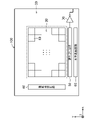
- the pixel cell array 20 is formed by arranging the pixel cells 10 in rows and columns. As will be described in detail later, the pixel cell 10 is composed of an APD1 (avalanche photodiode 1) and a plurality of transistors electrically connected to the APD1.
- APD1 active photodiode 1
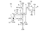
- the pixel cell 10 has an APD 1, a transfer transistor 3 (hereinafter sometimes referred to as TRN-TR3), and a reset transistor 4 (hereinafter sometimes referred to as RST-TR4). is doing. Further, the pixel cell 10 includes a floating diffusion portion 2 (hereinafter sometimes referred to as an FD portion 2), a count transistor 7 (hereinafter sometimes called a CNT-TR7) and a capacitor 8 (hereinafter sometimes called an MIM8). ) and The pixel cell 10 further has an amplification transistor 5 (hereinafter sometimes called SF-TR5) and a selection transistor 6 (hereinafter sometimes called SEL-TR6). Note that in the following description, when focusing on the circuit operation, each element in the pixel cell 10 may be generically called a pixel circuit.
- the TRN-TR3 is a field effect transistor (hereinafter sometimes referred to as a MISFET) whose source is connected to the cathode of the APD1 and whose drain is connected to the FD section 2.
- the drain of the TRN-TR3 and the FD section 2 is a common area.
- TRN-TR3 are N-channel MISFETs. That is, the source and drain are n-type impurity regions, and the region immediately below the gate is a p-type impurity region. Gates of TRN-TR3 are connected to the vertical scanning circuit 40 .
- SEL-TR6 is a MISFET whose drain is connected to the source of SF-TR5 and whose source is connected to VSL9. A gate of SEL-TR6 is connected to the vertical scanning circuit 40 . When the drive signal SEL is supplied from the vertical scanning circuit 40, the SEL-TR6 is turned on, and the output signal of the SF-TR5 is transferred to the VSL9 and further output to the readout circuit 50.
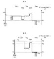
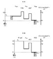
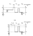
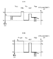
- FIG. 1 When the drive signal SEL is supplied from the vertical scanning circuit 40, the SEL-TR6 is turned on, and the output signal of the SF-TR5 is transferred to the VSL9 and further output to the readout circuit 50.
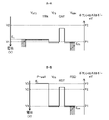
- Ec and EFN are displayed in each figure for reference.
- Ec indicates the lower end level of the conduction band of the semiconductor layer forming each part in the pixel cell 10 .
- E FN indicates the Fermi level of the n-type semiconductor layer forming each part.
- the vertical axis also shows the potential energy of electrons in each part in the pixel cell 10 . Since the potential energy of an electron is opposite to the magnitude relationship of the potential, the relationship of P3>P2>P1 is satisfied in each figure.
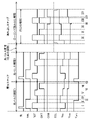
- the drive signal TRN is lowered to 0V, TRN-TR3 is turned off, and the exposure ends (period IV shown in FIG. 4).
- the driving signal CNT is lowered to 0V to turn off CNT-TR7 (period XI shown in FIG. 4).
- a voltage signal based on the amount of charge accumulated in the FD section 2 is output from the SF-TR5 and transferred to the VSL9 via the SEL-TR6.
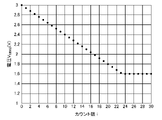
- FIG. 7 shows an example of the relationship between the photon count number and the capacitor voltage in the exposure step.
- the potential VFD of the FD section 2 is adjusted to a predetermined level for each exposure period. . That is, when photons are incident on the APD 1 during one exposure period, the charge amount accumulated in the FD portion 2 is constant.
- the charge accumulated in the FD section 2 is redistributed to the MIM 8 according to the ratio between the capacitance CFD of the FD section 2 and the capacitance CMIM of the MIM 8. .
- the pixel cell 10 has at least a CNT-TR7 connected to the FD section 2 and an MIM8 having one terminal connected to the front CNT-TR7.
- the number of elements in the pixel cell 10 can be reduced by one compared to the conventional configuration disclosed in Patent Document 2.
- the first reset transistor in Patent Document 2 can be omitted.
- the size of the pixel cell 10 can be reduced, and the solid-state imaging device 100 with higher integration than the conventional configuration disclosed in Patent Document 2 can be realized.
- the number of transistors directly connected to the APD 1 can be reduced compared to the conventional configuration disclosed in Patent Document 2.
- the first reset transistor in Patent Document 2 can be omitted.
- the number of transistors directly connected to the APD 1 can be reduced, so the amount of dark current flowing into the APD 1 can be reduced compared to the conventional configuration disclosed in Patent Document 2. This makes it possible to suppress deterioration in image quality.
- the potentials of the terminals of the MIM 8 connected to the capacitor signal line 42 can be changed to different levels.
- the difference between the reset level and the signal level can be increased, noise components can be removed, and a large-amplitude photodetection signal can be obtained. This makes it possible to accurately detect the number of photons incident on the APD 1 .
- the vertical scanning circuit 40 is configured to be able to apply voltages of three or more different levels to the gate of the RST-TR4. By doing so, the potential VFD of the FD section 2 is adjusted, and the amount of charge accumulated in the FD section 2 when photons are incident during one exposure period, and thus the charge accumulated in the MIM 8 Amount can be constant. As a result, the number of incident photons to the APD 1 can be detected without providing a dedicated circuit such as an analog-digital conversion circuit. That is, it is possible to accurately detect the number of times that photons are incident on the APD 1 while configuring the solid-state imaging device 100 with a simple configuration.
- the charges generated by the APD 1 are accumulated in the MIM 8 via the FD section 2 during the exposure period.
- the vertical scanning circuit 40 causes the VSL 9 to read out a photodetection signal based on the charge amount accumulated in the MIM 8 . By doing so, the number of times photons are incident on the APD 1 can be accurately detected.
- the magnitude of the photodetection signal output from the solid-state imaging device 100 corresponds to the number of exposure periods during which photons are incident on the APD1.
- the number of times photons are incident on the APD 1 can be accurately detected without providing a dedicated circuit such as an analog-digital conversion circuit.
- the level changing circuit sets the voltage of the power supply 11 so that the APD 1 operates in the linear multiplication mode.
- the determination circuit and the level change circuit may be provided outside the solid-state imaging device 100 .
Landscapes
- Engineering & Computer Science (AREA)
- Multimedia (AREA)
- Signal Processing (AREA)
- Solid State Image Pick-Up Elements (AREA)
Priority Applications (3)
| Application Number | Priority Date | Filing Date | Title |
|---|---|---|---|
| CN202280013571.1A CN116897542A (zh) | 2021-03-29 | 2022-03-22 | 固态成像元件 |
| JP2023511001A JPWO2022210070A1 (https=) | 2021-03-29 | 2022-03-22 | |
| US18/448,673 US12363460B2 (en) | 2021-03-29 | 2023-08-11 | Solid-state imaging sensor |
Applications Claiming Priority (2)
| Application Number | Priority Date | Filing Date | Title |
|---|---|---|---|
| JP2021055138 | 2021-03-29 | ||
| JP2021-055138 | 2021-03-29 |
Related Child Applications (1)
| Application Number | Title | Priority Date | Filing Date |
|---|---|---|---|
| US18/448,673 Continuation US12363460B2 (en) | 2021-03-29 | 2023-08-11 | Solid-state imaging sensor |
Publications (1)
| Publication Number | Publication Date |
|---|---|
| WO2022210070A1 true WO2022210070A1 (ja) | 2022-10-06 |
Family
ID=83456087
Family Applications (1)
| Application Number | Title | Priority Date | Filing Date |
|---|---|---|---|
| PCT/JP2022/012995 Ceased WO2022210070A1 (ja) | 2021-03-29 | 2022-03-22 | 固体撮像素子 |
Country Status (4)
| Country | Link |
|---|---|
| US (1) | US12363460B2 (https=) |
| JP (1) | JPWO2022210070A1 (https=) |
| CN (1) | CN116897542A (https=) |
| WO (1) | WO2022210070A1 (https=) |
Families Citing this family (1)
| Publication number | Priority date | Publication date | Assignee | Title |
|---|---|---|---|---|
| US20260059876A1 (en) * | 2024-08-23 | 2026-02-26 | Semiconductor Components Industries, Llc | Capacitor Structures |
Citations (3)
| Publication number | Priority date | Publication date | Assignee | Title |
|---|---|---|---|---|
| WO2018216400A1 (ja) * | 2017-05-25 | 2018-11-29 | パナソニックIpマネジメント株式会社 | 固体撮像素子、及び撮像装置 |
| WO2019186838A1 (ja) * | 2018-03-28 | 2019-10-03 | パナソニックIpマネジメント株式会社 | 固体撮像素子、固体撮像装置、固体撮像システム、固体撮像素子の駆動方法 |
| WO2021044770A1 (ja) * | 2019-09-06 | 2021-03-11 | パナソニックIpマネジメント株式会社 | 撮像装置 |
Family Cites Families (3)
| Publication number | Priority date | Publication date | Assignee | Title |
|---|---|---|---|---|
| JP4252078B2 (ja) | 2006-09-28 | 2009-04-08 | 三洋電機株式会社 | 光検出装置 |
| JP2017126846A (ja) * | 2016-01-13 | 2017-07-20 | ソニー株式会社 | 撮像素子、撮像素子の駆動方法、並びに、電子機器 |
| KR102476722B1 (ko) * | 2016-02-12 | 2022-12-14 | 에스케이하이닉스 주식회사 | 단위 픽셀 장치 및 그 동작 방법과 그를 이용한 씨모스 이미지 센서 |
-
2022
- 2022-03-22 WO PCT/JP2022/012995 patent/WO2022210070A1/ja not_active Ceased
- 2022-03-22 CN CN202280013571.1A patent/CN116897542A/zh active Pending
- 2022-03-22 JP JP2023511001A patent/JPWO2022210070A1/ja active Pending
-
2023
- 2023-08-11 US US18/448,673 patent/US12363460B2/en active Active
Patent Citations (3)
| Publication number | Priority date | Publication date | Assignee | Title |
|---|---|---|---|---|
| WO2018216400A1 (ja) * | 2017-05-25 | 2018-11-29 | パナソニックIpマネジメント株式会社 | 固体撮像素子、及び撮像装置 |
| WO2019186838A1 (ja) * | 2018-03-28 | 2019-10-03 | パナソニックIpマネジメント株式会社 | 固体撮像素子、固体撮像装置、固体撮像システム、固体撮像素子の駆動方法 |
| WO2021044770A1 (ja) * | 2019-09-06 | 2021-03-11 | パナソニックIpマネジメント株式会社 | 撮像装置 |
Also Published As
| Publication number | Publication date |
|---|---|
| US12363460B2 (en) | 2025-07-15 |
| CN116897542A (zh) | 2023-10-17 |
| US20230388676A1 (en) | 2023-11-30 |
| JPWO2022210070A1 (https=) | 2022-10-06 |
Similar Documents
| Publication | Publication Date | Title |
|---|---|---|
| CN110651366B (zh) | 固体摄像元件及摄像装置 | |
| US8159585B2 (en) | Image sensor pixel with gain control | |
| US8537259B2 (en) | Photoelectric conversion circuit and solid state imaging device including same | |
| US8217328B2 (en) | Low noise pixel readout circuit with high conversion gain | |
| JP7162251B2 (ja) | 撮像装置 | |
| US7427790B2 (en) | Image sensor with gain control | |
| JP5222240B2 (ja) | 光センサ回路、および光センサアレイ | |
| US8525896B2 (en) | Solid-state imaging apparatus | |
| US7626618B2 (en) | Solid-state image pickup device, driving method for solid-state image pickup device and image pickup apparatus | |
| US20150070549A1 (en) | Solid-state image device | |
| JP2009283552A (ja) | 固体撮像素子 | |
| JP4130307B2 (ja) | 固体撮像装置 | |
| US10999548B2 (en) | Pixel sensing circuit and driving method therefor, image sensor, and electronic device | |
| US20210329181A1 (en) | Imaging device and drive method therefor | |
| EP1850387B1 (en) | Solid-state image pickup device | |
| JP2018093297A (ja) | 光電変換装置、撮像システム | |
| US20060192234A1 (en) | Solid-state imaging device | |
| US12363460B2 (en) | Solid-state imaging sensor | |
| JP2013062733A (ja) | 固体撮像装置 | |
| EP2981069A1 (en) | Photoelectric conversion apparatus and photoelectric conversion system | |
| US11843884B1 (en) | HV driver for rolling clamp in image sensor | |
| US20240259708A1 (en) | Imaging device | |
| JP7402635B2 (ja) | 固体撮像素子および撮像装置、ならびに白キズ抑制方法 | |
| CN116491127A (zh) | 摄像装置 |
Legal Events
| Date | Code | Title | Description |
|---|---|---|---|
| 121 | Ep: the epo has been informed by wipo that ep was designated in this application |
Ref document number: 22780285 Country of ref document: EP Kind code of ref document: A1 |
|
| WWE | Wipo information: entry into national phase |
Ref document number: 202280013571.1 Country of ref document: CN |
|
| WWE | Wipo information: entry into national phase |
Ref document number: 2023511001 Country of ref document: JP |
|
| NENP | Non-entry into the national phase |
Ref country code: DE |
|
| 122 | Ep: pct application non-entry in european phase |
Ref document number: 22780285 Country of ref document: EP Kind code of ref document: A1 |