WO2022209764A1 - 画像表示装置の製造方法および画像表示装置 - Google Patents
画像表示装置の製造方法および画像表示装置 Download PDFInfo
- Publication number
- WO2022209764A1 WO2022209764A1 PCT/JP2022/010914 JP2022010914W WO2022209764A1 WO 2022209764 A1 WO2022209764 A1 WO 2022209764A1 JP 2022010914 W JP2022010914 W JP 2022010914W WO 2022209764 A1 WO2022209764 A1 WO 2022209764A1
- Authority
- WO
- WIPO (PCT)
- Prior art keywords
- light emitting
- insulating film
- layer
- light
- image display
- Prior art date
- Legal status (The legal status is an assumption and is not a legal conclusion. Google has not performed a legal analysis and makes no representation as to the accuracy of the status listed.)
- Ceased
Links
Images


Classifications
-
- H—ELECTRICITY
- H10—SEMICONDUCTOR DEVICES; ELECTRIC SOLID-STATE DEVICES NOT OTHERWISE PROVIDED FOR
- H10H—INORGANIC LIGHT-EMITTING SEMICONDUCTOR DEVICES HAVING POTENTIAL BARRIERS
- H10H20/00—Individual inorganic light-emitting semiconductor devices having potential barriers, e.g. light-emitting diodes [LED]
- H10H20/80—Constructional details
- H10H20/84—Coatings, e.g. passivation layers or antireflective coatings
-
- H—ELECTRICITY
- H10—SEMICONDUCTOR DEVICES; ELECTRIC SOLID-STATE DEVICES NOT OTHERWISE PROVIDED FOR
- H10H—INORGANIC LIGHT-EMITTING SEMICONDUCTOR DEVICES HAVING POTENTIAL BARRIERS
- H10H20/00—Individual inorganic light-emitting semiconductor devices having potential barriers, e.g. light-emitting diodes [LED]
- H10H20/01—Manufacture or treatment
- H10H20/011—Manufacture or treatment of bodies, e.g. forming semiconductor layers
- H10H20/013—Manufacture or treatment of bodies, e.g. forming semiconductor layers having light-emitting regions comprising only Group III-V materials
- H10H20/0133—Manufacture or treatment of bodies, e.g. forming semiconductor layers having light-emitting regions comprising only Group III-V materials with a substrate not being Group III-V materials
- H10H20/01335—Manufacture or treatment of bodies, e.g. forming semiconductor layers having light-emitting regions comprising only Group III-V materials with a substrate not being Group III-V materials the light-emitting regions comprising nitride materials
-
- H—ELECTRICITY
- H10—SEMICONDUCTOR DEVICES; ELECTRIC SOLID-STATE DEVICES NOT OTHERWISE PROVIDED FOR
- H10H—INORGANIC LIGHT-EMITTING SEMICONDUCTOR DEVICES HAVING POTENTIAL BARRIERS
- H10H20/00—Individual inorganic light-emitting semiconductor devices having potential barriers, e.g. light-emitting diodes [LED]
- H10H20/80—Constructional details
- H10H20/81—Bodies
- H10H20/819—Bodies characterised by their shape, e.g. curved or truncated substrates
- H10H20/82—Roughened surfaces, e.g. at the interface between epitaxial layers
-
- H—ELECTRICITY
- H10—SEMICONDUCTOR DEVICES; ELECTRIC SOLID-STATE DEVICES NOT OTHERWISE PROVIDED FOR
- H10H—INORGANIC LIGHT-EMITTING SEMICONDUCTOR DEVICES HAVING POTENTIAL BARRIERS
- H10H20/00—Individual inorganic light-emitting semiconductor devices having potential barriers, e.g. light-emitting diodes [LED]
- H10H20/80—Constructional details
- H10H20/81—Bodies
- H10H20/822—Materials of the light-emitting regions
- H10H20/824—Materials of the light-emitting regions comprising only Group III-V materials, e.g. GaP
- H10H20/825—Materials of the light-emitting regions comprising only Group III-V materials, e.g. GaP containing nitrogen, e.g. GaN
-
- H—ELECTRICITY
- H10—SEMICONDUCTOR DEVICES; ELECTRIC SOLID-STATE DEVICES NOT OTHERWISE PROVIDED FOR
- H10H—INORGANIC LIGHT-EMITTING SEMICONDUCTOR DEVICES HAVING POTENTIAL BARRIERS
- H10H20/00—Individual inorganic light-emitting semiconductor devices having potential barriers, e.g. light-emitting diodes [LED]
- H10H20/80—Constructional details
- H10H20/85—Packages
- H10H20/851—Wavelength conversion means
- H10H20/8515—Wavelength conversion means not being in contact with the bodies
-
- H—ELECTRICITY
- H10—SEMICONDUCTOR DEVICES; ELECTRIC SOLID-STATE DEVICES NOT OTHERWISE PROVIDED FOR
- H10H—INORGANIC LIGHT-EMITTING SEMICONDUCTOR DEVICES HAVING POTENTIAL BARRIERS
- H10H20/00—Individual inorganic light-emitting semiconductor devices having potential barriers, e.g. light-emitting diodes [LED]
- H10H20/80—Constructional details
- H10H20/85—Packages
- H10H20/857—Interconnections, e.g. lead-frames, bond wires or solder balls
-
- H—ELECTRICITY
- H10—SEMICONDUCTOR DEVICES; ELECTRIC SOLID-STATE DEVICES NOT OTHERWISE PROVIDED FOR
- H10W—GENERIC PACKAGES, INTERCONNECTIONS, CONNECTORS OR OTHER CONSTRUCTIONAL DETAILS OF DEVICES COVERED BY CLASS H10
- H10W90/00—Package configurations
-
- H—ELECTRICITY
- H10—SEMICONDUCTOR DEVICES; ELECTRIC SOLID-STATE DEVICES NOT OTHERWISE PROVIDED FOR
- H10H—INORGANIC LIGHT-EMITTING SEMICONDUCTOR DEVICES HAVING POTENTIAL BARRIERS
- H10H20/00—Individual inorganic light-emitting semiconductor devices having potential barriers, e.g. light-emitting diodes [LED]
- H10H20/01—Manufacture or treatment
- H10H20/011—Manufacture or treatment of bodies, e.g. forming semiconductor layers
- H10H20/018—Bonding of wafers
-
- H—ELECTRICITY
- H10—SEMICONDUCTOR DEVICES; ELECTRIC SOLID-STATE DEVICES NOT OTHERWISE PROVIDED FOR
- H10H—INORGANIC LIGHT-EMITTING SEMICONDUCTOR DEVICES HAVING POTENTIAL BARRIERS
- H10H20/00—Individual inorganic light-emitting semiconductor devices having potential barriers, e.g. light-emitting diodes [LED]
- H10H20/01—Manufacture or treatment
- H10H20/034—Manufacture or treatment of coatings
-
- H—ELECTRICITY
- H10—SEMICONDUCTOR DEVICES; ELECTRIC SOLID-STATE DEVICES NOT OTHERWISE PROVIDED FOR
- H10H—INORGANIC LIGHT-EMITTING SEMICONDUCTOR DEVICES HAVING POTENTIAL BARRIERS
- H10H20/00—Individual inorganic light-emitting semiconductor devices having potential barriers, e.g. light-emitting diodes [LED]
- H10H20/01—Manufacture or treatment
- H10H20/036—Manufacture or treatment of packages
- H10H20/0361—Manufacture or treatment of packages of wavelength conversion means
-
- H—ELECTRICITY
- H10—SEMICONDUCTOR DEVICES; ELECTRIC SOLID-STATE DEVICES NOT OTHERWISE PROVIDED FOR
- H10H—INORGANIC LIGHT-EMITTING SEMICONDUCTOR DEVICES HAVING POTENTIAL BARRIERS
- H10H20/00—Individual inorganic light-emitting semiconductor devices having potential barriers, e.g. light-emitting diodes [LED]
- H10H20/01—Manufacture or treatment
- H10H20/036—Manufacture or treatment of packages
- H10H20/0364—Manufacture or treatment of packages of interconnections
Definitions
- the embodiments of the present invention relate to an image display device manufacturing method and an image display device.
- micro LEDs which are minute light emitting elements, as self-luminous elements.
- a method of manufacturing a display device using micro LEDs a method of sequentially transferring individually formed micro LEDs to a driving circuit has been introduced.
- the image quality becomes full HD, 4K, 8K, etc.
- the number of micro LED elements increases.
- a huge amount of time is required for the transfer process.
- a connection failure or the like may occur between the micro LED and the drive circuit or the like, resulting in a decrease in yield.
- a known technique is to grow a semiconductor layer including a light-emitting layer on a Si substrate, form an electrode on the semiconductor layer, and then attach it to a circuit substrate on which a drive circuit is formed (see, for example, Patent Document 1).
- An embodiment of the present invention provides an image display device manufacturing method and an image display device in which the transfer process of light emitting elements is shortened and the yield is improved.
- a method for manufacturing an image display device includes steps of forming a layer including a first portion of single-crystal metal on a substrate, and forming a semiconductor layer including a light-emitting layer on the first portion. processing the semiconductor layer to form a light emitting device including a light emitting surface on the first portion and a top surface opposite to the light emitting surface; the substrate, a layer including the first portion, and forming a first insulating film covering the light emitting element; forming a circuit element on the first insulating film; forming a light shielding member between the circuit element and the light emitting element; forming a first insulating film and a second insulating film covering the circuit element; forming a first via penetrating the first insulating film and the second insulating film; The method includes forming a wiring layer, removing the substrate, and removing at least part of the first portion on the light emitting surface. The first via is provided between the wiring layer and the upper surface and electrically connects
- An image display device includes a light emitting element including a light emitting surface and an upper surface opposite to the light emitting surface; a first insulating film covering the light emitting element so as to expose the light emitting surface; a circuit element provided on the first insulating film; a light blocking member provided between the circuit element and the upper surface; a second insulating film covering the first insulating film and the circuit element; A first via provided through the first insulating film and the second insulating film, and a wiring layer provided on the second insulating film. The first via is provided between the wiring layer and the upper surface and electrically connects the wiring layer and the upper surface.
- the first insulating film includes a first surface on the light emitting surface side. The light emitting surface is provided in a concave portion relative to the first surface.
- An image display device comprises: a first semiconductor layer including a light emitting surface capable of forming a plurality of light emitting regions; a plurality of light emitting layers spaced apart from each other on the first semiconductor layer; a plurality of second semiconductors respectively provided on the plurality of light emitting layers, having a conductivity type different from that of the first semiconductor layer, and including a plurality of upper surfaces opposite to the surface on which the plurality of light emitting layers are provided; a first insulating film covering the first semiconductor layer, the plurality of light emitting layers, and the plurality of second semiconductor layers so as to expose the light emitting surface; a plurality of provided transistors; a light blocking member provided between the plurality of transistors and the plurality of top surfaces; the first insulating film and a second insulating film covering the plurality of transistors; a plurality of first vias provided through the film and the second insulating film; and a wiring layer provided on the second insulating film.
- the plurality of second semiconductor layers are separated by the first insulating film.
- the plurality of light emitting layers are separated by the first insulating film.
- the plurality of first vias are provided between the wiring layer and the plurality of upper surfaces, respectively, and electrically connect the wiring layer and the plurality of upper surfaces, respectively.
- the first insulating film includes a first surface on the light emitting surface side. The light emitting surface is provided in a concave portion relative to the first surface.
- An image display device comprises: a plurality of light emitting elements each including a light emitting surface and an upper surface opposite to the light emitting surface; 1 insulating film, a circuit element provided on the first insulating film, a light shielding member provided between the circuit element and the upper surface, and a second insulating film covering the first insulating film and the circuit element a film, a plurality of first vias provided through the first insulating film and the second insulating film, and a wiring layer provided on the second insulating film.
- the plurality of first vias are provided between the wiring layer and the plurality of upper surfaces, and electrically connect the wiring layer and the plurality of upper surfaces, respectively.
- the first insulating film includes a first surface on the side of the plurality of light emitting surfaces.
- the plurality of light emitting surfaces are provided in a concave portion relative to the first surface.
- a method for manufacturing an image display device is realized in which the transfer process of light emitting elements is shortened and the yield is improved.
- the present invention it is possible to reduce the size of the light-emitting element and realize a high-definition image display device.
- FIG. 1 is a schematic cross-sectional view illustrating part of an image display device according to a first embodiment; FIG. It is a typical enlarged view of the A section of FIG. 1 is a schematic block diagram illustrating an image display device according to a first embodiment; FIG. 1 is a schematic plan view illustrating part of an image display device according to a first embodiment; FIG.
- FIG. 1 is a schematic perspective view illustrating an image display device according to a first embodiment
- FIG. 1 is a schematic perspective view illustrating an image display device according to a first embodiment
- FIG. 1 is a schematic perspective view illustrating an image display device according to a first embodiment
- FIG. 5 is a schematic cross-sectional view illustrating part of an image display device according to a second embodiment
- FIG. 15 is a schematic enlarged view of part C of FIG. 14
- FIG. 5 is a schematic block diagram illustrating an image display device according to a second embodiment
- FIG. 11 is a schematic cross-sectional view illustrating a part of an image display device according to a third embodiment
- 10A to 10C are schematic cross-sectional views illustrating a part of the method for manufacturing the image display device of the third embodiment
- 10A to 10C are schematic cross-sectional views illustrating a part of the method for manufacturing the image display device of the third embodiment
- 10A to 10C are schematic cross-sectional views illustrating a part of the method for manufacturing the image display device of the third embodiment
- 10A to 10C are schematic cross-sectional views illustrating a part of the method for manufacturing the image display device of the third embodiment
- 10A to 10C are schematic cross-sectional views illustrating a part of the method for manufacturing the image display device of the third embodiment
- FIG. 11 is a schematic cross-sectional view illustrating part of an image display device according to a fourth embodiment; It is a schematic cross-sectional view illustrating a part of the manufacturing method of the image display device of the fourth embodiment. It is a schematic cross-sectional view illustrating a part of the manufacturing method of the image display device of the fourth embodiment. It is a schematic cross-sectional view illustrating a part of the manufacturing method of the image display device of the fourth embodiment. It is a schematic cross-sectional view illustrating a part of the manufacturing method of the image display device of the fourth embodiment.
- FIG. 11 is a schematic cross-sectional view illustrating part of an image display device according to a fifth embodiment; FIG.
- FIG. 11 is a schematic cross-sectional view illustrating part of an image display device according to a fifth embodiment;
- FIG. 11 is a schematic cross-sectional view illustrating a part of an image display device according to a sixth embodiment;
- FIG. 14 is a schematic cross-sectional view illustrating part of an image display device according to a sixth embodiment;
- FIG. 11 is a block diagram illustrating an image display device according to a seventh embodiment;
- FIG. FIG. 21 is a block diagram illustrating an image display device according to a modification of the seventh embodiment;
- FIG. 1 is a schematic cross-sectional view illustrating a part of the image display device according to this embodiment.
- FIG. 1 schematically shows the configuration of a sub-pixel 20 of the image display device of this embodiment.
- an XYZ three-dimensional coordinate system may be used.
- the light emitting elements 150 are arranged in a two-dimensional plane as shown in FIGS. 12 and 13, which will be described later.
- a light emitting element 150 is provided for each sub-pixel 20 .
- a two-dimensional plane on which the sub-pixels 20 are arranged is defined as an XY plane.
- the sub-pixels 20 are arranged along the X-axis direction and the Y-axis direction.
- FIG. 1 shows a cross section taken along the line BB' of FIG.
- cross-sectional views taken along a plurality of planes perpendicular to the XY plane, such as FIG. 1, do not show the X-axis and Y-axis, but show the Z-axis perpendicular to the XY plane. That is, in these figures, the plane perpendicular to the Z axis is the XY plane.
- the positive direction of the Z-axis is sometimes referred to as “up” or “upper”, and the negative direction of the Z-axis is referred to as “down” or “downward”.
- the direction is not limited.
- the length in the direction along the Z-axis is sometimes called height.
- the sub-pixel 20 has a light emitting surface 151S substantially parallel to the XY plane.
- the light emitting surface 151S is a surface that mainly emits light in the negative direction of the Z axis orthogonal to the XY plane.
- the light emitting surface mainly emits light in the negative direction of the Z axis.
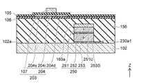
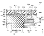
- the sub-pixel 20 of the image display device includes a light-emitting element 150, a light-shielding electrode (light-shielding member) 160a, a first interlayer insulating film 156, a transistor (circuit element) 103, and a second interlayer insulating film. It includes a film 108 , a via (first via) 161 a and a wiring layer 110 .
- the sub-pixel 20 further includes a color filter (wavelength converting member) 180 .
- the light emitting element 150 is provided on the color filter 180 .
- a first interlayer insulating film 156 is also provided on the color filter 180 .
- the surface of the light emitting element 150 on the color filter 180 is the light emitting surface 151S.
- the surface of the first interlayer insulating film 156 on the color filter 180 is the first surface 156S1.
- Light emitting surface 151S and first surface 156S1 are connected to color filter 180 via transparent resin layer 188 .
- the transparent resin layer 188 is provided to planarize the light emitting surface 151S and the first surface 156S1 and connect the color filter 180 thereto.
- the light emitting element 150 emits light through the light emitting surface 151S, the transparent resin layer 188 and the color filter 180.
- the light emitting element 150 is driven by the transistor 103 provided on the first interlayer insulating film 156 .
- the transistor 103 is a thin film transistor (TFT).
- Color filter 180 includes light shielding portion 181 and color conversion portion 182 .
- the color conversion section 182 is provided directly below the light emitting surface 151S of the light emitting element 150 according to the shape of the light emitting surface 151S.
- a portion of the color filter 180 other than the color conversion portion 182 is a light shielding portion 181 .
- the light shielding portion 181 is a so-called black matrix, which reduces blurring due to color mixture of light emitted from the adjacent color conversion portion 182, and makes it possible to display a clear image.
- the color conversion unit 182 has one layer or two layers or more.
- FIG. 1 shows a case where the color conversion section 182 has two layers. Whether the color conversion section 182 has one layer or two layers is determined by the color of the light emitted from the sub-pixel 20, that is, the wavelength.
- the color conversion section 182 is made up of two layers, a color conversion layer 183 and a filter layer 184 that allows red light to pass through.
- the color conversion section 182 is preferably made up of two layers, a color conversion layer 183 and a filter layer 184 that allows green light to pass through. If the emission color of the sub-pixels 20 is blue, one layer is preferred.
- the color conversion section 182 has two layers, one layer is the color conversion layer 183 and the other layer is the filter layer 184 .
- the color conversion layer 183 is stacked on the filter layer 184 , and the color conversion layer 183 is provided closer to the light emitting element 150 than the filter layer 184 is.
- the color conversion layer 183 converts the wavelength of light emitted by the light emitting element 150 into a desired wavelength.
- the light of 467 nm ⁇ 30 nm which is the wavelength of the light emitting element 150
- the light of 467 nm ⁇ 30 nm which is the wavelength of the light emitting element 150
- the light of 467 nm ⁇ 30 nm which is the wavelength of the light emitting element 150
- the light of 467 nm ⁇ 30 nm which is the wavelength of the light emitting element 150
- the filter layer 184 cuts off the wavelength component of the blue emission that remains without being color-converted by the color conversion layer 183 .
- the color of the light emitted by the sub-pixel 20 When the color of the light emitted by the sub-pixel 20 is blue, it may be output through the color conversion layer 183 or may be output as it is without the color conversion layer 183 .
- the wavelength of the light emitted by the light emitting element 150 When the wavelength of the light emitted by the light emitting element 150 is about 467 nm ⁇ 30 nm, the light may be output without passing through the color conversion layer 183 .
- the wavelength of the light emitted by the light emitting element 150 is set to 410 nm ⁇ 30 nm, it is preferable to provide the color conversion layer 183 in order to convert the wavelength of the output light to about 467 nm ⁇ 30 nm.
- the subpixel 20 may have the filter layer 184 even in the case of the blue subpixel 20 .
- the filter layer 184 that transmits blue light, minute external light reflection other than blue light generated on the surface of the light emitting element 150 is suppressed.
- the color filter 180 has a connection surface 180S.
- a transparent resin layer 188 is provided on the connection surface 180S.
- the light emitting element 150 and the first interlayer insulating film 156 are provided on the connection surface 180S with the transparent resin layer 188 interposed therebetween.
- the light emitting element 150 includes a light emitting surface 151S provided on the connection surface 180S.
- the light emitting element 150 includes an upper surface 153U provided on the opposite side of the light emitting surface 151S.
- the outer peripheral shape of light emitting surface 151S and upper surface 153U in XY plan view is square or rectangular, and light emitting element 150 is a prismatic element having light emitting surface 151S on connecting surface 180S.
- the cross section of the prism may be a polygon with pentagons or more.
- the light emitting element 150 is not limited to a prismatic element, and may be a cylindrical element.
- the light emitting element 150 includes an n-type semiconductor layer 151, a light emitting layer 152, and a p-type semiconductor layer 153.
- the n-type semiconductor layer 151, the light emitting layer 152 and the p-type semiconductor layer 153 are stacked in this order from the light emitting surface 151S toward the upper surface 153U.
- a light emitting surface 151S, which is the n-type semiconductor layer 151, is provided on the connection surface 180S. Therefore, the light emitting element 150 emits light in the negative direction of the Z axis via the transparent resin layer 188 and the color conversion portion 182 of the color filter 180 .
- the n-type semiconductor layer 151 includes a connecting portion 151a.
- the connection portion 151a is provided so as to protrude in one direction from the n-type semiconductor layer 151 on the connection surface 180S.
- the height of the connecting portion 151a from the light emitting surface 151S is the same as the height from the light emitting surface 151S to the n-type semiconductor layer 151 or lower than the height from the light emitting surface 151S to the n-type semiconductor layer 151.
- the n-type semiconductor layer 151 includes a connecting portion 151 a , and the connecting portion 151 a is part of the n-type semiconductor layer 151 .
- the connection portion 151a is connected to one end of the via 161k, and the n-type semiconductor layer 151 is electrically connected to the via 161k through the connection portion 151a.
- the shape of the light-emitting element 150 in XY plan view is, for example, substantially square or rectangular.
- the shape of the light emitting element 150 in the XY plan view is a polygon including a square, the corners of the light emitting element 150 may be rounded.
- the shape of the light-emitting element 150 in the XY plane view is cylindrical, the shape of the light-emitting element 150 in the XY plane view is not limited to a circle, and may be, for example, an ellipse.
- a gallium nitride-based compound semiconductor including a light-emitting layer such as In X Al Y Ga 1-XY N (0 ⁇ X, 0 ⁇ Y, X+Y ⁇ 1) is preferably used for the light-emitting element 150, for example.
- the gallium nitride-based compound semiconductor described above may be simply referred to as gallium nitride (GaN).
- the light emitting element 150 in one embodiment of the invention is a so-called light emitting diode.
- the wavelength of the light emitted by the light emitting element 150 may be in the range from the near-ultraviolet region to the visible light region, and is, for example, approximately 467 nm ⁇ 30 nm.
- the wavelength of the light emitted by the light emitting element 150 may be blue-violet emission of about 410 nm ⁇ 30 nm.
- the wavelength of the light emitted by the light emitting element 150 is not limited to the values described above, and may be an appropriate one.
- the light shielding electrode 160a is provided over the upper surface 153U.
- the light shielding electrode 160a is provided between the upper surface 153U and the via 161a, and electrically connects the upper surface 153U to one end of the via 161a.
- the light-shielding electrode 160a is made of a conductive material having a light-shielding property, and is formed with a thickness sufficient to exhibit the light-shielding property.
- the light shielding electrode 160 a realizes ohmic contact with the p-type semiconductor layer 153 and shields the light emitted upward from the light emitting element 150 and the scattered light.
- the light-shielding electrode 160a prevents light from reaching circuit elements including the transistor 103 provided above the light-emitting element 150, thereby preventing malfunction of the circuit elements.
- the first interlayer insulating film (first insulating film) 156 is provided on the transparent resin layer 188 on the first surface 156S1.
- the first interlayer insulating film 156 is provided on the connection surface 180S of the color filter 180 with a transparent resin layer 188 interposed therebetween.
- a first surface 156 S 1 of the first interlayer insulating film 156 is a surface connected to the transparent resin layer 188 .
- a first interlayer insulating film (first insulating film) 156 covers the side surface of the light emitting element 150 and the light shielding electrode 160a.
- the first interlayer insulating film 156 electrically isolates the adjacent light emitting devices 150 .
- the first interlayer insulating film 156 also electrically isolates the light-shielding electrodes 160a provided on the electrically isolated light emitting elements 150 .
- the first interlayer insulating film 156 electrically isolates the light-emitting element 150 and the light-shielding electrode 160a from circuit elements such as the transistor 103 and the like.
- First interlayer insulating film 156 provides a flat surface for forming circuit 101 including circuit elements such as transistor 103 . By covering the light emitting element 150, the first interlayer insulating film 156 protects the light emitting element 150 from thermal stress or the like when the transistor 103 or the like is formed.
- the first interlayer insulating film 156 is made of an organic insulating material.
- the organic insulating material used for the first interlayer insulating film 156 preferably has light reflectivity and is white resin.
- white resin By using a white resin for the first interlayer insulating film 156, it is possible to reflect light emitted in the lateral direction of the light emitting element 150 and return light caused by the interface between the light emitting surface 151S and the substrate 102, or the like. Therefore, the luminous efficiency of the light emitting device 150 is substantially improved.
- the white resin is formed by dispersing scattering fine particles having a Mie scattering effect in a transparent resin such as a silicon-based resin such as SOG (Spin On Glass) or a novolak-type phenol-based resin.
- the scattering microparticles are colorless or white, and have diameters that are about 1/10 to several times the wavelength of the light emitted by the light emitting element 150 .
- Scattering fine particles that are preferably used have a diameter that is about half the wavelength of light.
- such scattering fine particles include TiO 2 , Al 2 O 3 , ZnO, and the like.
- the white resin can also be formed by utilizing a large number of fine pores dispersed in the transparent resin.
- a SiO 2 film or the like formed by ALD (Atomic-Layer-Deposition) or CVD, for example, may be used over SOG or the like.
- the first interlayer insulating film 156 may be black resin. By using a black resin for the first interlayer insulating film 156, scattering of light within the sub-pixel 20 is suppressed, and stray light is suppressed more effectively. An image display device with suppressed stray light can display a sharper image.
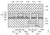
- a TFT lower layer film 106 is formed over the first interlayer insulating film 156 .
- the TFT lower layer film 106 is provided for the purpose of ensuring flatness during formation of the transistor 103 and protecting the TFT channel 104 of the transistor 103 from contamination during heat treatment.
- the TFT lower layer film 106 is an insulating film such as SiO 2 .
- the transistor 103 is formed on the TFT lower layer film 106 .
- circuit elements such as other transistors and capacitors are formed on the TFT lower layer film 106, and the circuit 101 is configured by wiring and the like.
- the transistor 103 corresponds to the driving transistor 26 in FIG. 3 described later.
- the selection transistor 24, the capacitor 28, and the like are circuit elements.
- Circuit 101 includes TFT channel 104 , insulating layer 105 , second interlayer insulating film 108 , vias 111 s and 111 d and first wiring layer 110 .
- the transistor 103 is a p-channel TFT in this example.
- Transistor 103 includes TFT channel 104 and gate 107 .
- the TFT channel 104 is preferably formed by a Low Temperature Poly Silicon (LTPS) process.
- LTPS Low Temperature Poly Silicon
- the TFT channel 104 is formed by polycrystallizing and activating the amorphous Si region formed on the TFT underlayer film 106 .
- laser annealing using a laser is used for polycrystallization and activation of the amorphous Si region.
- TFTs formed by the LTPS process have sufficiently high mobility.
- the TFT channel 104 includes regions 104s, 104i and 104d.
- the regions 104s, 104i, and 104d are all provided on the TFT lower layer film 106 .
- Region 104i is provided between region 104s and region 104d.
- the regions 104s and 104d contain impurities such as boron (B) and boron fluoride (BF) and form p-type semiconductor regions.
- the region 104s is ohmically connected to the via 111s, and the region 104d is ohmically connected to the via 111d.
- the gate 107 is provided on the TFT channel 104 via the insulating layer 105 .
- the insulating layer 105 is provided to insulate the TFT channel 104 from the gate 107 and to insulate it from other adjacent circuit elements.
- a channel is formed in region 104i.
- the insulating layer 105 is, for example, SiO2 .
- the insulating layer 105 may be a multilayer insulating layer containing SiO 2 , Si 3 N 4 or the like.
- the gate 107 may be made of, for example, polycrystalline Si, or may be made of a refractory metal such as W or Mo. Gate 107 is formed by, for example, CVD when it is formed of a polycrystalline Si film.
- a second interlayer insulating film 108 is provided on the gate 107 and the insulating layer 105 .
- the second interlayer insulating film 108 is made of the same material as the first interlayer insulating film 156, for example. That is, the second interlayer insulating film 108 is formed of an inorganic film such as white resin or SiO 2 .
- the second interlayer insulating film 108 also functions as a planarizing film for forming the wiring layer 110 .
- the vias 111 s and 111 d are provided through the second interlayer insulating film 108 and the insulating layer 105 .
- a wiring layer 110 is formed on the second interlayer insulating film 108 .
- the wiring layer 110 includes a plurality of wirings that can have different potentials.
- the wiring layer 110 includes wirings 110s, 110d, and 110k. These wirings 110s, 110d, and 110k are formed separately.
- a portion of the wiring 110s is provided above the region 104s. Another portion of the wiring 110s is connected to, for example, a power supply line 3 shown in FIG. 3, which will be described later.
- a portion of the wiring (first wiring) 110d is provided above the region 104d. Other portions of the wiring 110d are provided above the upper surface 153U.
- a portion of the wiring (second wiring) 110k is provided above the connection portion 151a. Line 110k is connected to, for example, ground line 4 shown in the circuit of FIG. 3, which will be described later.
- the reference numerals representing the wiring layers are displayed next to one wiring that constitutes the wiring layer.
- the symbols of the wiring layers 110 are displayed beside the wiring 110s.
- the via 111s is provided between the wiring 110s and the region 104s and electrically connects the wiring 110s and the region 104s.
- the via 111d is provided between the wiring 110d and the region 104d and electrically connects the wiring 110d and the region 104d.
- the wiring 110s is connected to the region 104s via the via 111s.
- Region 104 s is the source region of transistor 103 . Therefore, the source region of transistor 103 is electrically connected to power supply line 3 through via 111s and wiring 110s.
- the wiring 110d is connected to the region 104d via the via 111d.
- Region 104 d is the drain region of transistor 103 .
- a via (first via) 161a is provided to penetrate the second interlayer insulating film 108, the insulating layer 105, the TFT lower layer film 106 and the first interlayer insulating film 156 and reach the light shielding electrode 160a.
- the via 161a is provided between the wiring (first wiring) 110d and the light shielding electrode 160a, and electrically connects the wiring 110d and the light shielding electrode 160a. Therefore, the p-type semiconductor layer 153 is electrically connected to the drain region of the transistor 103 through the light shielding electrode 160a, the via 161a, the wiring 110d and the via 111d.
- a via (second via) 161k is provided so as to penetrate the second interlayer insulating film 108, the insulating layer 105, the TFT lower layer film 106 and the first interlayer insulating film 156 and reach the connection portion (first connection portion) 151a. ing.
- the via 161k is provided between the wiring (second wiring) 110k and the connecting portion 151a, and electrically connects the wiring 110k and the connecting portion 151a. Therefore, n-type semiconductor layer 151 is electrically connected to, for example, ground line 4 of the circuit of FIG.
- the wiring layer 110 and the vias 111s, 111d, 161a, and 161k are formed of, for example, Al, an alloy of Al, a laminated film of Al and Ti, or the like.
- Al is laminated on a Ti thin film, and Ti is further laminated on Al.
- a protective layer may be provided over the second interlayer insulating film 108 and the wiring layer 110 to protect them from the external environment.
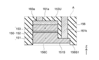
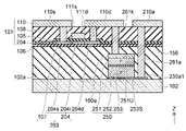
- FIG. 2 is a schematic enlarged view of part A in FIG. FIG. 2 shows in detail the positional relationship in the Z-axis direction between the first surface 156S1 of the first interlayer insulating film 156 and the light emitting surface 151S.
- the first surface 156S1 is one surface of the first interlayer insulating film 156 and is the surface on the light emitting surface 151S side.
- the recess 156C is formed by the first interlayer insulating film 156 and the light emitting surface 151S, and is recessed from the first surface 156S1 in the positive direction of the Z axis.
- the light emitting surface 151S is a surface substantially parallel to the first surface 156S1, and is provided at a position shifted in the positive direction of the Z axis from the first surface 156S1.
- the deviation in the Z-axis direction between the light emitting surface 151S and the first surface 156S1 is determined by the thickness of the single crystal metal layer for forming the light emitting element 150 in the description of the manufacturing method using FIGS. 5A to 9B described later. Almost equal.
- the recesses 156C are filled with the transparent resin layer 188 shown in FIG. 1, and the transparent resin layer 188 planarizes the first surface 156S1 and the light emitting surface 151S to some extent to facilitate the formation of color filters.
- FIG. 3 is a schematic block diagram illustrating the image display device according to this embodiment.
- the image display device 1 of this embodiment has a display area 2 .
- Sub-pixels 20 are arranged in the display area 2 .
- the sub-pixels 20 are arranged, for example, in a grid.
- n sub-pixels 20 are arranged along the X-axis and m sub-pixels 20 are arranged along the Y-axis.
- a pixel 10 includes a plurality of sub-pixels 20 that emit light of different colors.
- the sub-pixel 20R emits red light.
- Sub-pixel 20G emits green light.
- Sub-pixel 20B emits blue light.
- the emission color and brightness of one pixel 10 are determined by causing the three types of sub-pixels 20R, 20G, and 20B to emit light with desired brightness.
- One pixel 10 includes three sub-pixels 20R, 20G, 20B, and the sub-pixels 20R, 20G, 20B are linearly arranged on the X-axis, for example, as shown in FIG.
- Each pixel 10 may have sub-pixels of the same color arranged in the same column, or may have sub-pixels of different colors arranged in different columns as in this example.
- the image display device 1 further has a power line 3 and a ground line 4 .
- the power lines 3 and the ground lines 4 are laid out in a grid pattern along the array of the sub-pixels 20 .
- a power supply line 3 and a ground line 4 are electrically connected to each sub-pixel 20 to supply power to each sub-pixel 20 from a DC power supply connected between a power supply terminal 3a and a GND terminal 4a.
- a power terminal 3 a and a GND terminal 4 a are provided at ends of the power line 3 and the ground line 4 , respectively, and are connected to a DC power supply circuit provided outside the display area 2 .
- a positive voltage is supplied to the power supply terminal 3a with reference to the GND terminal 4a.
- the image display device 1 further has scanning lines 6 and signal lines 8 .
- the scanning lines 6 are laid in a direction parallel to the X-axis. That is, the scanning lines 6 are laid out along the array of the sub-pixels 20 in the row direction.
- the signal lines 8 are laid in a direction parallel to the Y-axis. That is, the signal lines 8 are wired along the array of the sub-pixels 20 in the column direction.
- the image display device 1 further has a row selection circuit 5 and a signal voltage output circuit 7 .
- Row selection circuit 5 and signal voltage output circuit 7 are provided along the outer edge of display area 2 .
- the row selection circuit 5 is provided along the Y-axis direction of the outer edge of the display area 2 .
- a row selection circuit 5 is electrically connected to the sub-pixels 20 in each column via scanning lines 6 and supplies a selection signal to each sub-pixel 20 .
- the signal voltage output circuit 7 is provided along the X-axis direction on the outer edge of the display area 2 .
- the signal voltage output circuit 7 is electrically connected to the sub-pixels 20 in each row via signal lines 8 and supplies signal voltages to each sub-pixel 20 .
- the sub-pixel 20 includes a light emitting element 22, a select transistor 24, a drive transistor 26, and a capacitor 28.
- the select transistor 24 may be labeled T1
- the drive transistor 26 may be labeled T2
- the capacitor 28 may be labeled Cm.
- the light emitting element 22 is connected in series with the driving transistor 26 .
- the driving transistor 26 is a p-channel TFT, and the drain electrode of the driving transistor 26 is connected to the anode electrode of the light emitting element 22 .
- the main electrodes of drive transistor 26 and select transistor 24 are the drain and source electrodes.
- An anode electrode of the light emitting element 22 is connected to the p-type semiconductor layer.
- a cathode electrode of the light emitting element 22 is connected to the n-type semiconductor layer.
- a series circuit of the light emitting element 22 and the driving transistor 26 is connected between the power supply line 3 and the ground line 4 .
- the drive transistor 26 corresponds to the transistor 103 in FIG. 1, and the light emitting element 22 corresponds to the light emitting element 150 in FIG.
- the current flowing through the light emitting element 22 is determined by the voltage applied between the gate and source of the driving transistor 26, and the light emitting element 22 emits light with a brightness corresponding to the current flowing through the light emitting element
- the select transistor 24 is connected between the gate electrode of the drive transistor 26 and the signal line 8 via the main electrode.
- a gate electrode of the selection transistor 24 is connected to the scanning line 6 .
- a capacitor 28 is connected between the gate electrode of the driving transistor 26 and the power supply line 3 .
- the row selection circuit 5 selects one row from the array of m rows of sub-pixels 20 and supplies a selection signal to the scanning line 6 .
- a signal voltage output circuit 7 supplies a signal voltage having the required analog voltage value to each sub-pixel 20 of the selected row.
- a signal voltage is applied across the gate-source of the drive transistors 26 of the sub-pixels 20 in the selected row.
- the signal voltage is held by capacitor 28 .
- the drive transistor 26 causes a current corresponding to the signal voltage to flow through the light emitting element 22 .
- the light emitting element 22 emits light with a brightness corresponding to the current that flows.
- the row selection circuit 5 sequentially switches the rows to be selected and supplies selection signals. That is, the row selection circuit 5 scans the rows in which the sub-pixels 20 are arranged. A current corresponding to the signal voltage flows through the light emitting elements 22 of the sequentially scanned sub-pixels 20 to emit light. The brightness of the sub-pixel 20 is determined by the current flowing through the light emitting element 22 . The sub-pixels 20 emit light with gradation based on the determined brightness, and an image is displayed in the display area 2 .
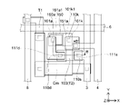
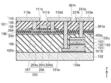
- FIG. 4 is a schematic plan view illustrating a part of the image display device of this embodiment.
- the BB' line represents the cutting line in the cross-sectional view of FIG. 1 and the like.
- the light emitting element 150 and the driving transistor 103 are stacked in the Z-axis direction with the first interlayer insulating film 156 interposed therebetween.
- Light emitting element 150 corresponds to light emitting element 22 in FIG.
- the driving transistor 103 corresponds to the driving transistor 26 in FIG. 3 and is also denoted as T2.
- the cathode electrode of the light emitting element 150 is provided by the connecting portion 151a.
- the connection portion 151 a is provided in a layer below the transistor 103 and the wiring layer 110 .
- the connecting portion 151a is electrically connected to the wiring 110k through the via 161k. More specifically, one end of the via 161k is connected to the connecting portion 151a. The other end of via 161k is connected to wiring 110k through contact hole 161k1.
- the anode electrode of the light emitting device 150 is provided by the p-type semiconductor layer 153 shown in FIG.
- the light shielding electrode 160 a is provided on the upper surface 153 U of the p-type semiconductor layer 153 .
- the light shielding electrode 160a is connected to one end of the wiring 110d via a via 161a. More specifically, one end of the via 161a is connected to the light shielding electrode 160a, and the other end of the via 161a is connected to the wiring 110d through the contact hole 161a1.
- the other end of the wiring 110d is connected to the drain electrode of the transistor 103 through the via 111d.
- the drain electrode of transistor 103 is region 104d shown in FIG.
- a source electrode of the transistor 103 is connected to the wiring 110s through the via 111s.
- the source electrode of transistor 103 is region 104s shown in FIG.
- the wiring layer 110 includes the power line 3 and the wiring 110 s is connected to the power line 3 .
- the ground line 4 is provided in a layer above the wiring layer including the wiring 110s.
- an interlayer insulating film is further provided on the wiring layer 110, and the ground line 4 is provided on the interlayer insulating film.
- the light emitting element 150 can be electrically connected to the wiring layer 110 provided above the light emitting element 150 by using the vias 161a and 161k.
- FIG. 5A to 9B are schematic cross-sectional views illustrating part of the method for manufacturing the image display device of this embodiment.
- the substrate 102 is prepared in the method for manufacturing the image display device of this embodiment.
- the substrate 102 is a translucent substrate, for example, a substantially rectangular glass substrate of approximately 1500 mm ⁇ 1800 mm.
- a metal layer 1130 is formed on the substrate surface 102a.
- the metal layer 1130 is patterned so as to leave a portion where the light emitting layer is formed after forming a layer of a metal material on the entire surface of the substrate surface 102a by sputtering or the like.
- the metal layer 1130 may be provided on the substrate surface 102a with a mask having a pattern with openings where the light emitting layer is to be formed, and then the patterned metal layer 1130 may be formed.
- the metal layer 1130 is formed using a metal material such as Cu or Hf. Sputtering or the like is preferably used to form the metal layer 1130 in order to form the film at a low temperature.
- the patterned metal layer 1130 is single-crystallized by annealing.
- an annealing process is performed to monocrystallize the entire patterned metal layer 1130 .
- an annealing treatment by laser irradiation for example, is preferably used.
- the metal layer 1130 can be single-crystallized while suppressing the influence of the temperature on the layers below the metal layer 1130 to a low temperature of about 400° C. to about 500° C. Therefore, the substrate 102 is made of glass or organic resin. etc. can be used.
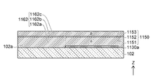
- the metal layer 1130 shown in FIG. 5A is formed with a metal seed layer (layer including the first portion) 1130a that is single-crystallized by annealing.
- a semiconductor layer 1150 is formed over the metal seed layer 1130a.
- the semiconductor layer 1150 includes an n-type semiconductor layer 1151, a light-emitting layer 1152, and a p-type semiconductor layer 1153 in this order from the metal seed layer 1130a toward the positive direction of the Z-axis.
- Non-Patent Document 1 Non-Patent Document 1
- Non-Patent Document 2 Non-Patent Document 1
- Such a low-temperature sputtering method is consistent with forming the semiconductor layer 1150 on a circuit substrate having TFTs and the like formed by the LTPS process.
- the semiconductor layer 1150 includes, for example, GaN, more specifically, In X Al Y Ga 1-XY N (0 ⁇ X, 0 ⁇ Y, X+Y ⁇ 1) and the like.
- crystal defects may occur due to the mismatch of crystal lattice constants, and crystals with crystal defects exhibit n-type. Therefore, as in this example, when the semiconductor layer 1150 is formed from the n-type semiconductor layer 1151 on the substrate 102, a large margin can be secured in the production process, so there is an advantage that the yield can be easily improved. be.
- a semiconductor layer 1150 of GaN is grown on the metal seed layer 1130a, which is monocrystallized over the entire surface, using an appropriate deposition technique, so that a monocrystallized light-emitting layer 1152 is formed on the metal seed layer 1130a.
- a semiconductor layer 1150 is formed.
- the semiconductor layer 1150 is formed within the region indicated by the two-dot chain line in FIG. 5B.
- an amorphous deposit 1162 containing the growth seed material such as Ga may be deposited on the substrate surface 102a where the metal seed layer 1130a does not exist.
- the deposits 1162 are stacked in the order of deposits 1162a, 1162b, and 1162c from the substrate surface 102a toward the positive direction of the Z-axis.
- Deposit 1162a was deposited during the formation of n-type semiconductor layer 1151
- deposit 1162b was deposited during the formation of light-emitting layer 1152
- deposit 1162c was deposited during the formation of p-type semiconductor layer 1153.
- a metal layer 1160 is formed on the semiconductor layer 1150 .
- metal layer 1160 is also formed over deposit 1162 . More specifically, metal layer 1160 is formed on p-type semiconductor layer 1153 and deposit 1162c.
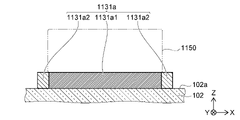
- FIG. 6A-6C show cross-sectional views of three types of patterning portions 1131a.
- the patterned portion 1131a is a portion formed by patterning the metal seed layer 1130a shown in FIG. 5B.
- FIG. 6A shows a state in which the entire patterned portion 1131a is single-crystallized.
- the patterning portion (first portion) 1131a is entirely monocrystallized. More specifically, the patterned portion 1131a is single-crystallized over the XY plane, and is single-crystallized from the surface of the patterned portion 1131a to the substrate surface 102a over the Z-axis direction.
- the semiconductor layer 1150 is formed over the patterned portion 1131a as indicated by the two-dot chain line in FIG. 6A.
- the patterned portion 1131a includes a single-crystallized portion (first portion) 1131a1 and a non-single-crystallized portion 1131a2.
- the single-crystallized portion 1131a1 is formed from the surface of the patterned portion 1131a to the substrate surface 102a along the Z-axis direction.
- the non-single-crystallized portion 1131a2 is formed so as to surround the single-crystallized portion 1131a1.
- the semiconductor layer 1150 is formed over the single-crystallized portion 1131a1 of the patterned portion 1131a, as indicated by the two-dot chain line in FIG. 6B.
- the patterned portion 1131a includes a single-crystallized portion (first portion) 1131a1 and a non-single-crystallized portion 1131a2.
- the single-crystallized portion 1131a1 is formed near the surface of the patterned portion 1131a in the Z-axis direction and does not reach the substrate surface 102a.
- the non-single-crystallized portion 1131a2 is formed around the single-crystallized portion 1131a1 as in FIG. 6B.
- the semiconductor layer 1150 is formed over the single-crystallized portion 1131a1 of the patterned portion 1131a, as indicated by the chain double-dashed line in FIG. 6C.
- An amorphous deposit containing, for example, Ga, which is a growth seed material, is deposited on non-single-crystallized portion 1131a2 and substrate surface 102a.
- the semiconductor layer 1150 is formed on the single-crystallized portion of the patterning portion 1131a. Therefore, the area of the single-crystallized portion (first portion) of the patterning portion 1131a when viewed in the XY plane is sufficiently larger than the area of the bottom surface of the light-emitting element.
- the perimeter is set to include the perimeter of the light emitting element. That is, in XY plane view, the outer circumference of the light emitting element 150 is arranged within the outer circumference of the single-crystallized portion.
- the metal material forming the metal layer 1130 shown in FIG. 5A is, for example, Cu or Hf.
- the metal material used for the metal layer 1130 is not limited to Cu or Hf as long as it is a metal material that can be single-crystallized by annealing. From the viewpoint of reducing thermal stress on the circuit board 100, a metal material that can be single-crystallized by annealing treatment at a lower temperature is preferable.
- the single-crystal metal metal seed layer 1130a is used as a seed to promote GaN crystal formation.
- a conductive buffer layer is provided on the metal seed layer 1130a, and the semiconductor layer is grown on the buffer layer by the above-described low-temperature sputtering method or the like.
- a graphene sheet may be used as the buffer layer.
- the metal layer 1160 and the semiconductor layer 1150 shown in FIG. 5B are processed into a desired shape by etching to form the light shielding electrode (light shielding member) 160a and the light emitting element 150.
- the connecting portion 151a is formed, and then etching is performed to form other portions and the light shielding electrode (light shielding member) 160a on the upper surface 153U.
- the light emitting element 150 having the connecting portion 151a projecting from the n-type semiconductor layer 151 above the substrate surface 102a in the positive direction of the X axis can be formed.
- a dry etching process for example, is used to form the light emitting element 150, and preferably anisotropic plasma etching (Reactive Ion Etching, RIE) is used.
- the metal seed layer 1130a shown in FIG. 5B is etched to form a seed plate (first portion) 130a.
- the outer circumference of the seed plate 130a in the XY plan view is formed so as to substantially match the outer circumference of the light emitting surface 151S of the light emitting element 150.
- the outer periphery of the seed plate 130a in XY plan view may be formed so as to include the outer periphery of the bottom surface 151B. That is, the outer circumference of the bottom surface 151B may be arranged within the outer circumference of the seed plate 130a in the XY plan view.
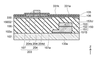
- a first interlayer insulating film (first insulating film) 156 is formed so as to cover the substrate surface 102a, the light emitting element 150 and the light shielding electrode 160a.
- the TFT lower layer film 106 is formed on the first interlayer insulating film 156 by, for example, CVD.
- a Si layer 1104 is formed on the formed TFT lower layer film 106 .
- the Si layer 1104 is an amorphous Si layer at the time of deposition, and after the deposition, a polycrystalline Si layer 1104 is formed by, for example, scanning an excimer laser pulse a plurality of times.
- the polycrystallized Si layer 1104 shown in FIG. 7B is processed into an island shape to form the TFT channel 104 .
- An insulating layer 105 is formed to cover the TFT lower layer film 106 and the TFT channel 104 .
- the insulating layer 105 functions as a gate insulating film.
- a gate 107 is formed on the TFT channel 104 with an insulating layer 105 interposed therebetween.
- a transistor (circuit element) 103 is formed by selectively doping an impurity such as B into the gate 107 and thermally activating it.
- the regions 104s and 104d are p-type active regions and function as the source and drain regions of the transistor 103, respectively.
- Region 104i is an n-type active region and functions as a channel.
- the transistor 103 is formed at a desired position on the TFT lower layer film 106 in this way.
- a second interlayer insulating film (second insulating film) 108 is provided to cover insulating layer 105 and gate 107 .
- An appropriate manufacturing method is applied to the formation of the second interlayer insulating film 108 according to the material of the second interlayer insulating film 108 .
- the second interlayer insulating film 108 is formed of SiO2 , techniques such as ALD and CVD are used.
- the flatness of the second interlayer insulating film 108 may be sufficient to form the wiring layer 110, and the flattening process may not necessarily be performed. If the planarization process is not performed on the second interlayer insulating film 108, the number of processes can be reduced. For example, when there is a portion where the thickness of the second interlayer insulating film 108 is thin around the light emitting element 150, the depth of the via holes for the vias 161a and 161k can be made shallow, so that sufficient opening can be achieved. caliber can be secured. Therefore, it becomes easy to ensure electrical connection through vias, and it is possible to suppress a decrease in yield due to defective electrical characteristics.
- Vias 161 a and 161 k are formed through the second interlayer insulating film 108 , insulating layer 105 , TFT lower layer film 106 and first interlayer insulating film 156 .
- a via (first via) 161a is formed by filling a conductive material into a via hole formed to reach the light shielding electrode 160a, and is electrically connected to the light shielding electrode 160a.
- the via (second via) 161k is formed by filling a conductive material into a via hole formed to reach the connecting portion (first connecting portion) 151a, and is electrically connected to the connecting portion 151a.
- Vias 111s and 111d are formed through the second interlayer insulating film 108 and the insulating layer 105 .
- the via 111s is formed to reach the region 104s.
- Via 111d is formed to reach region 104d.
- RIE for example, is used to form via holes for forming the vias 161a, 161k, 111s, and 111d.
- the wiring layer 110 is formed on the second interlayer insulating film 108 .
- Wirings 110k, 110d and 110s are formed.
- the wiring 110k is connected to one end of the via 161k.
- the wiring 110d is connected to one end of the via 161a and one end of the via 111d.
- the wiring 110s is connected to one end of the via 111s.
- the wirings 110k, 110d, and 110s may be formed simultaneously with the formation of the vias 161k, 111d, and 111s.
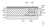
- an adhesive layer 1170 is formed on the second interlayer insulating film 108 and the wiring layer 110 , and a reinforcing substrate 1180 is attached to the adhesive layer 1170 .
- the reinforcing substrate 1180 is provided in order to maintain sufficient strength in subsequent processing, movement, etc. in the structure after removing the substrate 102 shown in FIG. 8B.
- the substrate 102 is removed. Simultaneously with the removal of substrate 102, seed plate 130a shown in FIG. 8B is also removed. Seed plate 130 a may be removed after removal of substrate 102 . Wet etching, laser lift-off, or the like is used to remove the substrate 102 and the seed plate 130a. Substrate 102 and seed plate 130a are removed to expose first surface 156S1 of first interlayer insulating film 156 and light emitting surface 151S.
- a transparent resin layer 188 is formed on the first surface 156S1 and the light emitting surface 151S.
- the transparent resin layer 188 is formed to fill the recess 156C of the first interlayer insulating film 156 shown in FIG. 2, forming a CF forming surface 188S for forming color filters.
- 10A to 10D are schematic cross-sectional views illustrating part of the method for manufacturing the image display device of this embodiment.
- 10A to 10D show a method of forming color filters by an inkjet method.
- a structure 1192 is prepared in which the CF forming surface 188S of the transparent resin layer 188 is exposed.
- the structure 1192 includes the transparent resin layer 188, the light emitting element 150 on the transparent resin layer 188, the adhesive layer 1170 and the reinforcing substrate 1180, as well as the first interlayer insulating film 156, the light shielding electrode 160a and the TFT lower layer film 106 shown in FIG. 9B. , TFT channels, insulating layer 105, gate 107, vias 111s, 111d, 161a and 161k, wiring layer 110, and the like.
- a light shielding portion 181 is formed in a region on the CF forming surface 188S and not including the light emitting surface 151S.
- the light shielding portion 181 is formed using, for example, screen printing, photolithography, or the like.
- the phosphor corresponding to the emitted color is ejected from the inkjet nozzle to form the color conversion layer 183.
- the phosphor colors the area on the CF forming surface 188S where the light shielding portion 181 is not formed.
- a fluorescent paint using a general phosphor material, a perovskite phosphor material, or a quantum dot phosphor material is used. It is preferable to use a perovskite phosphor material or a quantum dot phosphor material, since each emission color can be realized, and the monochromaticity and color reproducibility can be improved.
- a drying process is performed at an appropriate temperature and time. The thickness of the coating film when colored is set thinner than the thickness of the light shielding portion 181 .
- the color conversion layer 183 is not formed if the color conversion section is not formed. Further, in the case of forming a blue color conversion layer for a blue light emitting sub-pixel, if only one color conversion layer is sufficient for the color conversion part, the thickness of the coating film of the blue phosphor is preferably equal to the thickness of the color conversion layer. The thickness is the thickness of the filter layer 184 laminated on 183 and is about the same as the thickness of the light shielding portion 181 .
- the paint for the filter layer 184 is ejected from an inkjet nozzle.
- the paint is applied over the coating film of the phosphor.
- the total thickness of the coating film of the phosphor and paint is approximately the same as the thickness of the light shielding portion 181 .
- FIG. 11 is a schematic cross-sectional view illustrating a part of a modification of the method for manufacturing the image display device of this embodiment.
- the figure above the arrow is structure 1192 .
- Structure 1192 includes transparent resin layer 188, light emitting element 150, adhesive layer 1170, reinforcing substrate 1180, and the like shown in FIG. 9B.
- the figure below the arrow shows the glass substrate 186, the color filter 180a adhered to the glass substrate 186, and the transparent thin film adhesion layer 189 that adheres the color filter 180a to the structure 1192.
- FIG. 11 is a schematic cross-sectional view illustrating a part of a modification of the method for manufacturing the image display device of this embodiment.
- the figure above the arrow is structure 1192 .
- Structure 1192 includes transparent resin layer 188, light emitting element 150, adhesive layer 1170, reinforcing substrate 1180, and the like shown in FIG. 9B.
- the figure below the arrow shows the glass substrate 186, the color filter 180a
- the arrows represent the situation where the color filter 180a is attached to the structure 1192 together with the glass substrate 186 and the transparent thin film adhesive layer 189.
- FIG. 11 for some components of the structure 1192, the symbols and the components themselves including the symbols are omitted in order to avoid complication. Components in the structure 1192 that are not shown are the first interlayer insulating film 156, the circuit 101, and the vias 161a and 161k shown in FIG. 9B.
- the color filter (wavelength conversion member) 180a includes a light blocking portion 181a, color conversion layers 183R, 183G and 183B, and a filter layer 184a.
- the light shielding part 181a has the same function as in the case of the inkjet method.
- the color conversion layers 183R, 183G, and 183B are formed with the same function and the same material as in the case of the inkjet system.
- the filter layer 184a also has the same function as in the inkjet method.
- the color filter 180a is adhered to the structure 1192 on one side.
- the other surface of the color filter 180a is adhered to the glass substrate 186.
- a transparent thin film adhesive layer 189 is provided on one surface of the color filter 180a, and is adhered to the exposed surface of the transparent resin layer 188 of the structure 1192 via the transparent thin film adhesive layer 189.
- the color filter 180a has color converters arranged in the positive direction of the X-axis in order of red, green, and blue.
- a red color conversion layer 183R is provided on the layer on the transparent thin film adhesive layer 189 side.
- a green color conversion layer 183G is provided on the layer on the transparent thin film adhesive layer 189 side.
- a filter layer 184a is provided on the layer on the glass substrate 186 side for each of the red color conversion section and the green color conversion section.
- a single-layer color conversion layer 183B is provided from the glass substrate 186 side to the transparent thin film adhesive layer 189 side.
- the filter layer 184a may be provided on the glass substrate 186 side as in the case of other colors.
- the frequency characteristics of the filter layer 184 may be the same for all the colors of the color converters, or may be different for each color of the color converters.
- a light shielding portion 181a is provided between each color conversion portion.
- the positions of the color conversion layers 183R, 183G, and 183B are aligned with the positions of the light emitting elements 150, and the color filter 180a is attached to the structure 1192 via the transparent thin film adhesive layer 189. Attached.
- the reinforcing substrate 1180 is removed together with the adhesive layer 1170, but the image display device may be constructed without removing the reinforcing substrate 1180 and the adhesive layer 1170.
- the color filters 180 and 180a are formed in the structure 1192 including the light emitting element 150 and the circuit 101 to form sub-pixels.
- an appropriate method is selected from inkjet methods, film methods, and other methods that can equally form color filters. According to the formation of the color filter 180 by the ink jet method, it is possible to omit the step of attaching the film and the like, and it is possible to manufacture the image display device 1 shown in FIG. 3 at a lower cost.
- the color conversion layer 183 be as thick as possible in order to improve the color conversion efficiency.
- the color conversion layer 183 is too thick, the emitted light of the color-converted light is approximated to Lambertian, whereas the emission angle of the blue light that is not color-converted is limited by the light shielding portion 181. .
- the display color of the displayed image is dependent on the viewing angle.
- the thickness of the color conversion layer 183 should be about half the size of the opening of the light shielding portion 181 in order to match the light distribution of the light of the sub-pixel provided with the color conversion layer 183 with the light distribution of the blue light that is not color-converted. is desirable.
- the pitch of the sub-pixels 20 is about 30 ⁇ m, so the thickness of the color conversion layer 183 is preferably about 15 ⁇ m.
- the color conversion material is made of spherical phosphor particles, it is preferable to stack them in a close-packed structure in order to suppress light leakage from the light emitting element 150 .
- the particle size of the phosphor material forming the color conversion layer 183 is preferably about 5 ⁇ m or less, more preferably about 3 ⁇ m or less.
- FIG. 12 is a schematic perspective view illustrating the image display device according to this embodiment.
- the image display device of this embodiment includes a light emitting circuit section 172 having a large number of light emitting elements 150 on a color filter 180 .
- the light emitting circuit section 172 includes the light emitting element 150 as well as the light shielding electrode 160 a and the first interlayer insulating film 156 .
- a circuit 101 including circuit elements including a transistor 103 and the like is provided on the light emitting circuit portion 172 via the TFT lower layer film 106 shown in FIG.
- the circuit 101 and the light emitting circuit section 172 are electrically connected via the vias 161a and 161k shown in FIG.
- FIG. 13 is a schematic perspective view illustrating an image display device according to a modification of this embodiment.
- the color filter 180 is provided in the image display device of the first embodiment described above.
- the image display device may emit monochromatic light without providing the color filter.
- the light emitting element 150 is formed by etching the semiconductor layer 1150 crystal-grown on the substrate 102 . After that, the light emitting element 150 is covered with a first interlayer insulating film 156 , and the circuit 101 including circuit elements such as the transistor 103 for driving the light emitting element 150 is formed on the first interlayer insulating film 156 . Therefore, the manufacturing process can be significantly shortened compared to individually transferring individual light emitting elements onto the substrate 102 .
- the metal layer 1130 formed on the substrate 102 is single-crystallized to form the metal seed layer 1130a, which serves as a seed for crystal growth of the semiconductor layer 1150.
- the metal layer 1130 can be single-crystallized by laser annealing treatment, so that sufficiently high productivity can be realized.
- a 4K image display device has more than 24 million sub-pixels
- an 8K image display device has more than 99 million sub-pixels.
- Forming such a large number of light-emitting elements individually and mounting them on a circuit board requires an enormous amount of time. Therefore, it is difficult to realize an image display device using micro LEDs at a realistic cost.
- the yield decreases due to connection failures during mounting, etc., and further cost increases are unavoidable. effect is obtained.
- the light emitting element 150 is formed after the entire semiconductor layer 1150 is deposited on the metal seed layer 1130a formed on the substrate 102. Therefore, the transfer step of the light emitting element 150 is omitted. can be reduced. Therefore, in the manufacturing method of the image display device 1 of the present embodiment, the transfer process time can be shortened and the number of processes can be reduced as compared with the conventional manufacturing method.
- the light emitting element 150 can be arranged in self-alignment by appropriately patterning the metal seed layer 1130a. Therefore, it is not necessary to align the light-emitting element on the substrate 102, and the light-emitting element 150 can be easily miniaturized, which is suitable for high-definition displays.
- the light-emitting elements 150 and the circuit elements formed on the upper layers of the light-emitting elements 150 are electrically connected by forming vias, so that a uniform connection structure can be achieved. can be realized, and a decrease in yield can be suppressed.
- the light-emitting element 150 formed on the glass substrate as described above is covered with the first interlayer insulating film 156, and a drive circuit including a TFT is formed on the flattened surface using the LTPS process or the like. , a scanning circuit, or the like can be formed.
- the LTPS process has the advantage of being able to use existing flat panel display manufacturing processes and plants, and can reduce thermal stress on the underlying light-emitting elements 150 and the like, improving yield. becomes possible.
- the light emitting element 150 formed in a layer below the transistor 103 and the like is formed by forming a via penetrating the first interlayer insulating film 156, the TFT lower layer film 106, the insulating layer 105 and the second interlayer insulating film 108.
- the transistor 103 is formed above the light emitting element 150, and the light shielding electrode 160a is formed over the upper surface 153U of the light emitting element 150. Therefore, upward scattered light emitted from the light emitting element 150 is suppressed from reaching the transistor 103 by the light shielding electrode 160a. Therefore, malfunction of the transistor 103 is prevented.
- the light shielding electrode 160a By appropriately selecting a conductive material for the light shielding electrode 160a, high light reflectivity can be imparted. Since the light-shielding electrode 160a has light reflectivity, it is possible to reflect upward scattered light and the like toward the light-emitting surface 151S, thereby substantially improving the light-emitting efficiency.
- FIG. 14 is a schematic cross-sectional view illustrating a part of the image display device according to this embodiment.
- the configurations of the light-emitting element 250 and the transistor 203 are different from those of the other embodiments described above.
- the light emitting surface 253S of the light emitting element 250 is provided by the p-type semiconductor layer 253, and the transistor 203 is n-channel, unlike the other embodiments described above.
- the p-type semiconductor layer 253 and the via 261a are connected by the connection plate 230a, which is also different from the other embodiments described above.
- the same reference numerals are given to the same components as in other embodiments, and detailed description thereof will be omitted as appropriate.
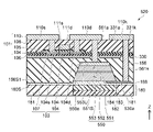
- the image display device of this embodiment includes sub-pixels 220 .
- the sub-pixel 220 includes a light emitting element 250, a light shielding electrode 160a, a first interlayer insulating film 156, a transistor (circuit element) 203, a second interlayer insulating film 108, a via (first via) 261k, and a wiring layer. 110 and.
- the light emitting element 250 is provided on the color filter 180 .
- a first interlayer insulating film 156 covering the side surface of the light emitting element 250 is also provided on the color filter 180 .
- the surface of the light emitting element 250 on the color filter 180 is the light emitting surface 253S.
- the surface of the first interlayer insulating film 156 on the color filter 180 is the first surface 156S1.
- the light emitting surface 253S and the first surface 156S1 are connected to the color filter 180 via the transparent resin layer 188.
- the transparent resin layer 188 is provided to planarize the light emitting surface 253S and the first surface 156S1 and connect the color filter 180 thereto.
- connection plate (second connection portion) 230a is a plate-like member having both sides. One surface of the connection plate 230a is connected to the surface of the p-type semiconductor layer 253 including the light emitting surface 253S. The connection plate 230a is provided so as to protrude in one direction above the color filter 180 from a surface including the light emitting surface 253S. One end of the via 261a is connected to the surface of the connection plate 230a connected to the surface including the light emitting surface 253S. The surface of the connection plate 230 a opposite to the surface connected to one end of the via 261 a is covered with a transparent resin layer 188 .
- the light emitting element 250 emits light via the light emitting surface 253S, the transparent resin layer 188 and the color filter 180.
- the light emitting element 250 includes an upper surface 251U provided on the opposite side of the light emitting surface 253S.
- the light emitting element 250 is a prismatic or cylindrical element, as in the other embodiments described above.
- the light emitting element 250 includes a p-type semiconductor layer 253, a light emitting layer 252, and an n-type semiconductor layer 251.
- the p-type semiconductor layer 253, the light emitting layer 252 and the n-type semiconductor layer 251 are laminated in this order from the light emitting surface 253S toward the upper surface 251U.
- the light emitting surface 253 S is provided by the p-type semiconductor layer 253 .
- the upper surface 251U is the surface opposite to the light emitting surface 253S.
- the light emitting element 250 has the same shape in XY plan view as the light emitting element 150 of the other embodiment described above. An appropriate shape is selected according to the layout of circuit elements and the like.
- the light emitting element 250 is a light emitting diode similar to the light emitting element 150 of the other embodiments described above. That is, the wavelength of the light emitted by the light emitting element 250 is, for example, blue light emission of approximately 467 nm ⁇ 30 nm, or blue-violet light emission of approximately 410 nm ⁇ 30 nm.
- the wavelength of the light emitted by the light emitting element 250 is not limited to the values described above, and may be any appropriate value.
- the transistor 203 is provided on the TFT lower layer film 106 .
- the transistor 203 is an n-channel TFT.
- Transistor 203 includes TFT channel 204 and gate 107 .
- transistor 203 is formed by an LTPS process or the like, similar to the other embodiments described above.
- the circuit 101 includes a TFT channel 204, an insulating layer 105, a second interlayer insulating film 108, vias 111s and 111d, and a wiring layer 110.
- the TFT channel 204 includes regions 204s, 204i and 204d. Regions 204 s , 204 i and 204 d are provided on TFT lower layer film 106 .
- the regions 204s and 204d are doped with impurities such as phosphorus (P) and activated to form n-type semiconductor regions.
- the region 204s is ohmically connected to the via 111s.
- the region 204d is ohmically connected to the via 111d.
- the gate 107 is provided above the TFT channel 204 via the insulating layer 105 .
- the insulating layer 105 insulates the TFT channel 204 and the gate 107 .
- a channel is formed in region 204i when a higher voltage is applied to gate 107 than region 204s.
- the current flowing between regions 204s and 204d is controlled by the voltage of gate 107 on region 204s.
- the TFT channel 204 and the gate 107 are formed by the same material and manufacturing method as those of the TFT channel 104 and the gate 107 in the other embodiments described above.
- the wiring layer 110 includes wirings 110s, 110d, and 210a.
- a portion of the wiring 210a (second wiring) is provided above the connection plate 230a.
- the other portion of interconnection 210a is connected, for example, to power supply line 3 shown in FIG. 16, which will be described later.
- the vias 111s and 111d are provided through the second interlayer insulating film .
- the via 111s is provided between the wiring 110s and the region 204s.
- the via 111s electrically connects the wiring 110s and the region 204s.
- the via 111d is provided between the wiring 110d and the region 204d.
- the via 111d electrically connects the wiring 110d and the region 204d.
- the vias 111s and 111d are formed with the same material and manufacturing method as in the other embodiments described above.
- a via (first via) 261k is provided so as to penetrate the second interlayer insulating film 108, the insulating layer 105, the TFT lower layer film 106 and the first interlayer insulating film 156 and reach the light shielding electrode 160a.
- the via 261k is provided between the wiring (first wiring) 110d and the light shielding electrode 160a, and electrically connects the wiring 110d and the light shielding electrode 160a. Therefore, the n-type semiconductor layer 251 is electrically connected to the region 204d forming the drain electrode of the transistor 203 through the light shielding electrode 160a, the via 261k, the wiring 110d and the via 111d.
- a via (second via) 261a is provided to penetrate the second interlayer insulating film 108, the insulating layer 105, the TFT lower layer film 106 and the first interlayer insulating film 156 and reach the connection plate (second connection portion) 230a. ing.
- the via 261a is provided between the wiring (second wiring) 210a and the connection plate 230a, and electrically connects the wiring 210a and the connection plate 230a. Therefore, p-type semiconductor layer 253 is electrically connected to, for example, power line 3 of the circuit of FIG. 16 via connection plate 230a, via 261a and wiring 210a.
- FIG. 15 is a schematic enlarged view of part C of FIG. 14 .
- FIG. 15 shows in detail the positional relationship in the Z-axis direction between the first surface 156S1 of the first interlayer insulating film 156 and the light emitting surface 253S, as well as the connection relationship between the connection plate 230a and the surface including the light emitting surface 253S. ing.
- the first surface 156S1 is the surface of the first interlayer insulating film 156 on the light emitting surface 253S side.
- the first interlayer insulating film 156 has a first surface 156S1.
- the recess 256C is formed by the first interlayer insulating film 156, the connection plate 230a and the light emitting surface 253S.
- the recess 256C is surrounded by the connection plate 230a and the light emitting surface 253S of the first interlayer insulating film 156, and is recessed from the first surface 156S1 in the positive direction of the Z axis.
- connection plate 230a is connected to the light emitting surface 253S on the surface connected to one end of the via 261a.
- a surface 230S on the opposite side of the surface connected to one end of the via 261a is a surface on substantially the same plane as the first surface 156S1.
- the light-emitting surface 253S is located in the positive direction of the Z-axis from the first surface 156S1 and the surface 230S of the connection plate 230a, and is a plane substantially parallel to the first surface 156S1 and the surface 230S.
- the deviation of the position of the light emitting surface 253S from the positions of the first surface 156S1 and the surface 230S is approximately equal to the length of the connection plate 230a in the Z-axis direction, that is, the thickness of the connection plate 230a.
- the recess 256C is filled with the transparent resin layer 188 shown in FIG. 14, and the light emitting surface 253S is connected to the color filter through the transparent resin layer 188 filled in the recess 256C.
- FIG. 16 is a schematic block diagram illustrating the image display device of this embodiment.
- the image display device 201 of this embodiment includes a display area 2 , a row selection circuit 205 and a signal voltage output circuit 207 .
- the display area 2 for example, sub-pixels 220 are arranged in a grid pattern on the XY plane, as in the other embodiments described above.
- Pixel 10 includes a plurality of sub-pixels 220 that emit light of different colors, as in the other embodiments described above.
- Sub-pixel 220R emits red light.
- Subpixel 220G emits green light.
- Sub-pixel 220B emits blue light. The emission color and brightness of one pixel 10 are determined by causing the three types of sub-pixels 220R, 220G, and 220B to emit light with desired brightness.
- One pixel 10 includes three sub-pixels 220R, 220G, 220B, and the sub-pixels 220R, 220G, 220B are linearly arranged on the X-axis, for example, as in this example.
- Each pixel 10 may have sub-pixels of the same color arranged in the same column, or may have sub-pixels of different colors arranged in different columns as in this example.
- the sub-pixel 220 includes a light emitting element 222, a select transistor 224, a drive transistor 226, and a capacitor 228.
- select transistor 224 may be labeled T1
- drive transistor 226 may be labeled T2
- capacitor 228 may be labeled Cm.
- the light emitting element 222 is provided on the power line 3 side, and the drive transistor 226 connected in series with the light emitting element 222 is provided on the ground line 4 side.
- the driving transistor 226 is connected to the lower potential side than the light emitting element 222 is.
- the drive transistor 226 is an n-channel transistor.
- a select transistor 224 is connected between the gate electrode of the drive transistor 226 and the signal line 208 .
- a capacitor 228 is connected between the gate electrode of the drive transistor 226 and the power supply line 3 .
- the row selection circuit 205 and the signal voltage output circuit 207 supply signal voltages of polarities different from those in the above-described other embodiments to the signal line 208 in order to drive the drive transistor 226, which is an n-channel transistor.
- the row selection circuit 205 supplies selection signals to the scanning lines 206 so as to sequentially select one row from the array of m rows of sub-pixels 220 .
- a signal voltage output circuit 207 supplies a signal voltage having the required analog voltage value to each sub-pixel 220 of the selected row.
- the drive transistors 226 of the sub-pixels 220 in the selected row pass current through the light emitting elements 222 according to the signal voltage.
- the light-emitting element 222 emits light with luminance according to the current that flows.
- 17A to 19B are schematic cross-sectional views illustrating part of the method for manufacturing the image display device of this embodiment.
- the substrate 102 described in connection with FIG. 5A of the other embodiment described above is used.
- the substrate 102 has a metal layer 1130 formed on the substrate surface 102a.
- a semiconductor layer 1150 is formed over the single-crystallized metal seed layer 1130a.
- a p-type semiconductor layer 1153, a light emitting layer 1152 and an n-type semiconductor layer 1151 are formed in this order from the metal seed layer 1130a toward the positive direction of the Z-axis.
- the semiconductor layer 1150 is formed over the metal seed layer 1130a as shown within the chain double-dashed line in FIG. 17A.
- an amorphous deposit 1162 containing the growth seed material such as Ga may be deposited on the substrate surface 102a where the metal seed layer 1130a is not present.
- the deposits 1162 are stacked in the order of deposits 1162d, 1162e, and 1162f from the substrate surface 102a toward the positive direction of the Z-axis.
- Deposit 1162d is shown deposited during formation of p-type semiconductor layer 1153
- deposit 1162e is deposited during formation of light emitting layer 1152
- deposit 1162f is shown deposited during formation of n-type semiconductor layer 1151.
- it is not limited to this.
- a metal layer 1160 is formed on the semiconductor layer 1150 .
- metal layer 1160 is also formed over deposit 1162 . More specifically, metal layer 1160 is formed on n-type semiconductor layer 1151 and on deposit 1162f.
- a light shielding electrode 160a, a light emitting element 250 and a connection plate 230a1 are formed.
- the light shielding electrode 160a is formed in the same manner as in the other embodiments described above.
- Connection plate 230a1 is formed by etching metal seed layer 1130a shown in FIG. 17A. After forming the connection plate 230a1, the light emitting element 250 is formed.
- connection plate 230a1 is formed so as to protrude from the light emitting element 250 in one direction above the substrate surface 102a.
- the outer periphery of the connection plate 230a1 is set so as to include the outer periphery of the light emitting element 250 when the light emitting element 250 is projected onto the connection plate 230a1 in XY plan view. That is, the outer circumference of the light emitting element 250 is arranged within the outer circumference of the connection plate 230a1.
- the projecting portion of the connection plate 230a1 is formed so as to secure a region for connecting one end of the via 261a shown in FIG. 19A, which will be described later.
- connection plate 230a1 is processed into the connection plate 230a shown in FIG. 14 in a later step. Since the p-type semiconductor layer 253 of the light emitting device 250 is connected to the via 261a through the connection plate 230a shown in FIG. It is molded into a single prismatic or cylindrical shape without forming.
- the first interlayer insulating film 156 is formed.
- the first interlayer insulating film 156 is formed to cover the substrate surface 102a, the connection plate 230a1, the light emitting element 250 and the light shielding electrode 160a.
- the TFT lower layer film 106 is formed on the first interlayer insulating film 156, and the Si layer 1104 is formed on the TFT lower layer film 106 and polycrystallized.
- the polycrystallized Si layer 1104 shown in FIG. 18A is processed into islands to form TFT channels 204 .
- An insulating layer 105 is formed to cover the TFT lower layer film 106 and the TFT channel 204 .
- the insulating layer 105 functions as a gate insulating film.
- a gate 107 is formed on the TFT channel 204 with an insulating layer 105 interposed therebetween.
- a transistor (circuit element) 203 is formed by selectively doping the gate 107 with an impurity such as P and thermally activating it.
- the regions 204s and 204d are n-type active regions and function as the source and drain regions of the transistor 203, respectively.
- Region 204i is a p-type active region and functions as a channel.
- the second interlayer insulating film 108 is formed covering the insulating layer 105 and the transistor 203 .
- Vias 111s and 111d penetrating the second interlayer insulating film 108 and the insulating layer 105 are formed.
- a via 261k is formed by filling a via hole formed to reach the light shielding electrode 160a through the second interlayer insulating film 108, the insulating layer 105, the TFT lower layer film 106 and the first interlayer insulating film 156 with a conductive material. .
- the via 261k is electrically connected to the light shielding electrode 160a.
- a via hole formed to reach connection plate 230a1 through second interlayer insulating film 108, insulating layer 105, TFT lower layer film 106 and first interlayer insulating film 156 is filled with a conductive material to form via 261a. .
- Via 261a is electrically connected to connection plate 230a1.
- Wirings 110s, 110d and 210a of the wiring layer 110 are connected to vias 111s, 111d, 261k and 261a, respectively.
- an adhesion layer 1170 is formed on the second interlayer insulating film 108 and the wiring layer 110, and a reinforcing substrate 1180 is adhered to the adhesion layer 1170. As shown in FIG. 19B, an adhesion layer 1170 is formed on the second interlayer insulating film 108 and the wiring layer 110, and a reinforcing substrate 1180 is adhered to the adhesion layer 1170. As shown in FIG. 19B, an adhesion layer 1170 is formed on the second interlayer insulating film 108 and the wiring layer 110, and a reinforcing substrate 1180 is adhered to the adhesion layer 1170. As shown in FIG.
- connection plate (first portion) 230a1 shown in FIG. 19A is processed to expose the light emitting surface 253S to form the connection plate (second connection portion) 230a.
- the connection plate 230a is formed by etching so as to leave a portion connected to the surface including the light emitting surface 253S.
- the formation of connection plate 230a forms recess 256C.
- a transparent resin layer is formed covering the first surface 156S1, the light emitting surface 253S, and the surface 230S of the connection plate 230a, and a color filter is formed via the transparent resin layer.
- a sub-pixel 220 is formed.
- the effect of the image display device of this embodiment will be described.
- the image display device of this embodiment has the effect of shortening the time required for the transfer process for forming the light emitting element 250 and reducing the number of processes, as in the other embodiments described above. .
- the polarity of the TFT to p-channel, it is possible to use the light-emitting surface 253S as the p-type semiconductor layer 253 . Therefore, there are merits such as an improvement in the degree of freedom in layout of circuit elements and in circuit design.
- connection plate 230a is made of a metal material and can have high electrical conductivity. Therefore, the p-type semiconductor layer 253 on the light emitting surface 253S side can be connected to the via 261a with low resistance.
- FIG. 20 is a schematic cross-sectional view illustrating part of the image display device according to this embodiment.
- This embodiment differs from the other embodiments described above in that the light-emitting element 150 whose light-emitting surface 151S is provided by the n-type semiconductor layer 151 is driven by the n-channel transistor 203 .
- This embodiment differs from the other embodiments described above in that a light shielding layer 330 is provided between the light emitting element 150 and the transistor 203 .
- the light emitting element 150 of this embodiment also differs from the other embodiments described above in that the light emitting surface 151S is roughened.
- the same reference numerals are given to the same components as in the other embodiments described above, and detailed description thereof will be omitted as appropriate.
- the image display device of this embodiment includes sub-pixels 320 .
- the sub-pixel 320 includes a light emitting element 150, a light shielding electrode 160a, a first interlayer insulating film 156, a light shielding layer 330, a transistor 203, a second interlayer insulating film 108, a via (first via) 361a, and wiring. and a layer 110 .
- Subpixel 320 further includes color filter 180 .
- the light emitting element 250 is provided on the color filter 180 and has a roughened light emitting surface 151S.
- a transparent resin layer 188 is provided between the roughened light emitting surface 151S and the color filter 180 .
- the transparent resin layer 188 is also provided on the first surface 156S1 of the first interlayer insulating film 156, and the light emitting element 150 and the first interlayer insulating film 156 are arranged on the color filter 180 via the transparent resin layer 188. is provided.
- the position of the light emitting surface 151S is shifted in the positive direction of the Z axis from the position of the first surface 156S1, and the transparent resin layer 188 forms the color filter 180. In order to do so, a plane that is flattened to some extent is formed.
- the light-emitting element 150 has an n-type semiconductor layer 151, a light-emitting layer 152 and a p-type semiconductor layer 153 stacked in this order from a light-emitting surface 151S toward an upper surface 153U.
- the n-type semiconductor layer 151 includes a connecting portion 151a.
- the connection portion 151a is provided so as to protrude in one direction from the n-type semiconductor layer 151 on the connection surface 180S.
- the connecting portion 151a is provided so as to protrude in a direction different from that in the first embodiment.
- the shape and configuration of the connecting portion 151a are the same as in the first embodiment, and the shape and configuration of the light emitting element 150 are also the same as in the first embodiment.
- One end of a via 361k is connected to the connecting portion 151a.
- the light shielding layer 330 is provided between the first interlayer insulating film 156 and the second interlayer insulating film 108 . Between the first interlayer insulating film 156 and the second interlayer insulating film 108, the TFT lower layer film 106 and the insulating layer 105 are provided. and the TFT lower layer film 106 . That is, the light shielding layer 330 is provided over the second surface 156S2 opposite to the first surface 156S1. The light shielding layer 330 is provided over the entire surface, except for a portion, between the first interlayer insulating film 156 and the TFT lower layer film 106 .
- the light shielding layer 330 is made of a light shielding material.
- the material of the light shielding layer 330 is made of, for example, a metal material having light reflectivity as in this example, regardless of whether or not it is conductive as long as it has a light shielding property.
- the light shielding layer 330 includes through holes 331a and 331k.
- the through-hole 331a is provided at a position through which the via 361a of the light shielding layer 330 passes when viewed from the XY plane.
- the diameter of the through hole 331a is set larger than the diameter of the via 361a so that the light shielding layer 330 does not contact the via 361a when the via 361a is passed through the through hole 331a.
- the through-hole 331k is provided at a position through which the via 361k of the light shielding layer 330 passes in the XY plan view.
- the diameter of the through-hole 331k is set larger than the diameter of the via 361k so that the light-shielding layer 330 does not come into contact with the via 361k when the via 361k is passed through the through-hole 331k.
- the via 361a is provided so as to penetrate the second interlayer insulating film 108, the insulating layer 105, the TFT lower layer film 106, the light shielding layer 330 and the first interlayer insulating film 156 and reach the light shielding electrode 160a.
- the via 361k penetrates the second interlayer insulating film 108, the insulating layer 105, the TFT lower layer film 106, the light shielding layer 330 and the first interlayer insulating film 156, and is provided to reach the connecting portion 151a.
- the light shielding layer 330 is made of a metal material in the above description, the light shielding layer 330 may be made of a non-conductive black resin.
- the via holes are formed together with the first interlayer insulating film 156 and the like without previously forming the through holes 331k and 331a having diameters larger than those of the vias 361k and 361a. Vias can be formed by filling with a conductive material.
- the light shielding layer 330 is provided so as to cover the TFT channel 204 .
- the light shielding layer 330 is formed so as to include the periphery of the TFT channel 204 when the TFT channel 204 is projected onto the light shielding layer 330 in the XY plan view. That is, the outer periphery of the TFT channel 204 is arranged inside the light shielding layer 330 in the XY plan view. Even if scattered light or the like is emitted upward from the light emitting element 150 provided below the TFT channel 204 by the light shielding layer 330, the scattered light or the like is shielded by the light shielding layer 330, and the scattered light or the like is blocked by the light shielding layer 330. , the TFT channel can hardly be reached, so that malfunction of the transistor 203 can be suppressed.
- the light shielding layer 330 is desirable for the light shielding layer 330 to be provided over the entire surface between the first interlayer insulating film 156 and the second interlayer insulating film 108 as in this example. It is not limited to one member.
- the light shielding layer 330 may be separately provided in a portion directly below the TFT channel 204 and a portion directly above the light emitting element 150 .
- the light shielding layer 330 is not connected to any potential, but may be connected to a specific potential such as ground potential or power supply potential.
- the light shielding layer 330 has a plurality of separated portions, all of them may be connected to a common potential, or each portion may be connected to a different potential.
- both the light-shielding electrode 160a and the light-shielding layer 330 function as light-shielding members for circuit elements including the TFT channel 204.
- the double light shielding member suppresses the light from reaching the circuit element, thereby sufficiently preventing malfunction of the circuit element.
- the wiring layer 110 is provided on the second interlayer insulating film 108 .
- the wiring layer 110 includes wirings 110s, 110d, and 310a.
- the via 111s is provided between the wiring 110s and the region 204s and electrically connects the wiring 110s and the region 204s.
- the via 111d is provided between the wiring 110d and the region 204d and electrically connects the wiring 110d and the region 204d.
- the wiring 110s is connected to the region 204s via the via 111s.
- Region 204 s is the source region of transistor 203 . Therefore, the source region of transistor 203 is electrically connected to, for example, ground line 4 shown in FIG. 16 through via 111s and line 110s.
- the wiring 110d is connected to the region 204d through the via 111d.
- Region 204 d is the drain region of transistor 203 .
- One end of the wiring 110d is provided above the connecting portion 151a.
- One end of the wiring 310a is provided above the light emitting element 150 and the light shielding electrode 160a.
- Wiring 310a is electrically connected to power supply line 3 in FIG. 16, for example.
- the via 361k is provided between the wiring 110d and the connecting portion 151a, and electrically connects the wiring 110d and the connecting portion 151a. Therefore, the drain region of the transistor 203 is electrically connected to the n-type semiconductor layer 151 through the via 111d, the wiring 110d, the via 361k and the connecting portion 151a.
- the via 361a is provided between the wiring 310a and the light shielding electrode 160a, and electrically connects the wiring 310a and the light shielding electrode 160a. Therefore, the p-type semiconductor layer 153 is electrically connected to the power line 3 through the light shielding electrode 160a, the via 361a and the wiring 310a.
- 21A to 23 are schematic cross-sectional views illustrating part of the method for manufacturing the image display device of this embodiment.
- the steps up to and including the steps described with reference to FIG. 7A of the first embodiment are applied in the same manner as in the first embodiment.
- the steps after FIG. 21A are applied after the step of FIG. 7A.
- the projecting direction of the connecting portion 151a is different from that in FIG. 7A.
- a light shielding layer (light shielding member) 330 is formed over the second surface 156S2 of the first interlayer insulating film 156.
- Through holes 331a and 331k are formed to penetrate the light shielding layer 330 and expose the second surface 156S2.
- the TFT lower layer film 106 is formed on the light shielding layer 330 and the second surface 156S2, and the Si layer 1104 is formed on the TFT lower layer film 106. As shown in FIG. 21B, the TFT lower layer film 106 is formed on the light shielding layer 330 and the second surface 156S2, and the Si layer 1104 is formed on the TFT lower layer film 106. As shown in FIG. 21B, the TFT lower layer film 106 is formed on the light shielding layer 330 and the second surface 156S2, and the Si layer 1104 is formed on the TFT lower layer film 106. As shown in FIG.
- the Si layer 1104 is processed to form the TFT channel 204, the insulating layer 105 and the gate 107 are formed, and the transistor 203 is formed. These steps can be performed in the same manner as in the second embodiment using the LTPS process.
- a second interlayer insulating film 108 is formed covering the insulating layer 105 and the gate 107, and vias 111s, 111d, 361k, and 361a are formed.
- a wiring layer 110 is formed on the second interlayer insulating film 108, a via 111s is connected to the wiring 110s, a via 111d and a via 361k are connected to the wiring 110d, and a via 361a is connected to the wiring 310a.
- an adhesive layer 1170 is applied on the second interlayer insulating film 108 and the wiring layer 110, and the reinforcing substrate 1180 is adhered by the adhesive layer 1170. As shown in FIG. 23, an adhesive layer 1170 is applied on the second interlayer insulating film 108 and the wiring layer 110, and the reinforcing substrate 1180 is adhered by the adhesive layer 1170. As shown in FIG. 23, an adhesive layer 1170 is applied on the second interlayer insulating film 108 and the wiring layer 110, and the reinforcing substrate 1180 is adhered by the adhesive layer 1170. As shown in FIG.
- the substrate 102 and seed plate 130a shown in FIG. 22B are removed sequentially or simultaneously by wet etching or laser lift-off.
- the exposed light emitting surface 151S is roughened. Wet etching, for example, is used to roughen the light emitting surface 151S.
- a transparent resin layer is formed to cover the first surface 156S1 and the light emitting surface 151S, color filters are formed, and sub-pixels are formed.
- the time for the transfer process for forming the light emitting element 150 can be shortened and the number of processes can be reduced, as in the other embodiments described above.
- the n-type semiconductor layer 151 having a resistance lower than that of the p-type is used as the light-emitting surface 151S
- the n-type semiconductor layer 151 can be formed thick and the light-emitting surface 151S can be sufficiently roughened.
- the emitted light is diffused by roughening the light emitting surface 151S. Therefore, even a small light emitting element 150 can be used as a light source with a sufficient light emitting area. .
- the light-emitting element 150 having the light-emitting surface 151S as the n-type semiconductor layer 151 can be driven by the n-channel transistor 203 . Therefore, the degree of freedom in circuit configuration is increased, and design efficiency can be improved.
- the light shielding layer 330 is provided between the first interlayer insulating film 156 and the second interlayer insulating film 108 . That is, the light shielding layer 330 is provided between the light emitting element 150 and the transistor 203 . Therefore, even if scattered light or the like is emitted upward from the light emitting element 150, the emitted light is less likely to reach the TFT channel 204, and malfunction of the transistor 203 can be prevented.
- the light shielding layer 330 can be made of a conductive material such as metal, and the light shielding layer 330 can be connected to any potential.
- a portion of the light shielding layer 330 may be placed directly under a switching element such as the transistor 203 and connected to a ground potential, a power supply potential, or the like to help suppress noise.
- the light-shielding layer 330 is not limited to application in this embodiment, and can be commonly applied to sub-pixels in the other embodiments described above and other embodiments described later. Even when applied to other embodiments, the same effect as described above can be obtained.
- a light-emitting element having a connecting portion can employ a roughened light-emitting surface as in the case of this embodiment. Specifically, it can be applied to the light emitting element 150 in the case of the first embodiment, and the light emitting element 150 in the case of the fourth embodiment described later is an example in which surface roughening is applied. Moreover, it can also be applied to a semiconductor layer 650 of a sixth embodiment, which will be described later. By applying roughening of the light-emitting surface to these constituent elements of the light-emitting element, the above effects can be obtained.
- FIG. 24 is a schematic cross-sectional view illustrating a part of the image display device of this embodiment.
- This embodiment differs from the third embodiment in that the light shielding electrode 160a shown in FIG. 20 is not provided, and is otherwise the same as the third embodiment.
- the same reference numerals are given to the same components as in the other embodiments described above, and detailed description thereof will be omitted as appropriate.
- the image display device of this embodiment includes sub-pixels 420 .
- the sub-pixel 420 includes the light emitting element 150, the first interlayer insulating film 156, the light shielding layer 330, the transistor 203, the second interlayer insulating film 108, the via 361a, and the wiring layer 110.
- Subpixel 420 further includes color filter 180 .
- the via 361a is provided between the wiring 310a and the upper surface 153U, and electrically connects the wiring 310a and the upper surface 153U.
- the light shielding layer 330 is provided between the first interlayer insulating film 156 and the second interlayer insulating film 108, and is formed in the same manner as in the third embodiment. That is, the light-shielding layer 330 is provided so as to cover the TFT channel 204, and more specifically, the light-shielding layer 330 is formed so as to cover the TFT channel 204 when the TFT channel 204 is projected onto the light-shielding layer 330 in XY plan view. 204 is set to include the entire perimeter. That is, the periphery of the TFT channel 204 is arranged within the periphery of the light shielding layer 330 in the XY plan view. Therefore, scattered light emitted upward from the light emitting element 150 is blocked by the light shielding layer 330, and the transistor 203 including the TFT channel 204 is prevented from malfunctioning due to the light.
- 25A to 26B are schematic cross-sectional views illustrating part of the method for manufacturing the image display device of this embodiment.
- the steps up to and including the steps described with reference to FIG. 5A of the first embodiment are applied in the same manner as in the first embodiment.
- the steps after FIG. 25A are applied after the step of FIG. 5A.
- a semiconductor layer 1150 is formed over the single-crystallized metal seed layer 1130a.
- the semiconductor layer 1150 includes an n-type semiconductor layer 1151, a light-emitting layer 1152, and a p-type semiconductor layer 1153 in this order from the metal seed layer 1130a toward the positive direction of the Z-axis.
- the semiconductor layer 1150 For forming the semiconductor layer 1150, a technique similar to that of the other embodiments described above is used, preferably a low-temperature sputtering method is used.
- the semiconductor layer 1150 is formed in the area indicated by the chain double-dashed line on the metal seed layer 1130a, and in the other area, an amorphous deposit 1162 containing Ga, which is a growth seed material, may be deposited. are also the same as in the other embodiments described above.
- a light shielding layer 330 is formed over the second surface 156S2 of the first interlayer insulating film 156. As shown in FIG. Through holes 331a and 331k are formed in the light shielding layer 330, and the second surface 156S2 is exposed from the through holes 331a and 331k.
- the TFT lower layer film 106 is formed on the light shielding layer 330 and the second surface 156S2, and the transistor 203 is formed on the TFT lower layer film 106.
- the procedure for forming the transistor 203 is the same as in the second embodiment and the third embodiment.
- a second interlayer insulating film 108 is formed covering the insulating layer 105 and the gate 107, vias 111s, 111d, 361k and 361a are formed, and the wiring layer 110 is formed.
- the via 361a is formed to penetrate the second interlayer insulating film 108, the insulating layer 105, the TFT lower layer film 106, the light shielding layer 330 and the first interlayer insulating film 156 and reach the upper surface 153U. It is formed by filling the via hole with a conductive material.
- a reinforcing substrate 1180 is adhered via an adhesive layer 1170 shown in FIG. 23, and the substrate 102 and seed plate 130a shown in FIG. 26B are removed.
- the exposed light emitting surface 151S is roughened to form a color filter through the transparent resin layer 188 shown in FIG.
- the effect of the image display device of this embodiment will be described.
- the image display device of this embodiment has the effect of shortening the time required for the transfer process for forming the light emitting element 150 and reducing the number of processes, as in the case of the other embodiments described above. .
- the step of forming the light shielding electrode can be omitted.
- FIG. 27 is a schematic cross-sectional view illustrating part of the image display device of this embodiment.
- the configurations of the light emitting element 550 and the light shielding electrode 560a are different from those of the other embodiments.
- Other components are the same as in other embodiments described above.
- the same constituent elements are denoted by the same reference numerals, and detailed description thereof will be omitted as appropriate.
- the light emitting element 550 is provided on the color filter 180.
- a first interlayer insulating film 156 covering the side surface of the light emitting element 550 is also provided on the color filter 180 .
- the surface of the light emitting element 550 on the color filter 180 is a light emitting surface 551S.
- the position of the light emitting surface 551S is shifted in the positive direction of the Z axis from the position of the first surface 156S1.
- a transparent resin layer 188 is formed over the light emitting surface 551S and the first surface 156S1, and the light emitting element 550 and the first interlayer insulating film 156 are provided on the color filter 180 via the transparent resin layer 188. .
- connection plate 530a is a plate-like member having two surfaces. One surface of the connection plate 530a is connected to the surface including the light emitting surface 551S.
- the connection plate 530a is provided on the connection surface 180S of the color filter 180 so as to protrude in one direction from the light emitting surface 551S.
- One end of the via 561k is connected to the surface where the connection plate 530a is connected to the surface including the light emitting surface 551S.
- a transparent resin layer 188 is provided over the surface of the connection plate 530a opposite to the surface to which the vias 561k are connected.
- connection plate 530a has the same function as the connection plate 230a in the case of the second embodiment shown in FIG. That is, the connection plate 530a is made of a conductive material and electrically connects the light emitting surface 551S and the via 561k.
- the light emitting element 550 includes a light emitting surface 551S and an upper surface 553U opposite to the light emitting surface.
- the light emitting element 550 has an n-type semiconductor layer 551, a light emitting layer 552 and a p-type semiconductor layer 553 stacked in this order from a light emitting surface 551S toward an upper surface 553U.
- the light emitting element 550 has a truncated pyramid or conical shape whose area in XY plane view gradually decreases from the light emitting surface 551S toward the upper surface 553U.
- the light shielding electrode 560a is provided on the upper surface 553U of the light emitting element 550 and has a truncated pyramid or truncated cone shape continuous from the top of the light emitting element 550 .
- the light shielding layer 330 is provided between the TFT lower layer film 106 and the first interlayer insulating film 156 .
- the light shielding layer 330 is the same as that described with reference to FIG. 20 in the third embodiment. Therefore, the light shielding layer 330 is provided so as to cover the TFT channel 104, can block light emitted from the light emitting element 550, and can prevent the transistor 103 including the TFT channel 104 from malfunctioning.
- the via 561k is provided to penetrate the second interlayer insulating film 108, the insulating layer 105, the TFT lower layer film 106, the light shielding layer 330 and the first interlayer insulating film 156 and reach the connection plate 530a.
- the via 561k is provided between the wiring 110k and the connection plate 530a to electrically connect the wiring 110k and the connection plate 530a.
- the via 561a is provided so as to penetrate the second interlayer insulating film 108, the insulating layer 105, the TFT lower layer film 106, the light shielding layer 330 and the first interlayer insulating film 156 and reach the light shielding electrode 560a.
- the via 561a is provided between the wiring 110d and the light shielding electrode 560a, and electrically connects the wiring 110d and the light shielding electrode 560a.
- Other components are the same as in the above-described second embodiment, and detailed description thereof will be omitted.
- FIG. 28 is an enlarged view of the portion of the light emitting element 550 in FIG. 27, showing in detail the relationship between the light emitting surface 551S and the side surface 555a.
- the light emitting surface 551S is a plane substantially parallel to the XY plane.
- the first surface 156S1 of the first interlayer insulating film 156 is also a plane substantially parallel to the XY plane.
- the light emitting element 550 and the first interlayer insulating film 156 are provided on the connection surface 180S of the color filter via the transparent resin layer 188, and the light emission surface 551S and the first surface 156S1 are substantially parallel to the connection surface 180S. It is the surface. Note that the position of the light emitting surface 551S is shifted in the positive direction of the Z-axis from the position of the first surface 156S1, as in the other embodiments described above.
- first interlayer insulating film 156 is described as being made of transparent resin.
- the effect on the refractive index is small and can be neglected.
- a side surface 555a of the light emitting element 550 is a surface between the upper surface 553U and the light emitting surface 551S and a surface adjacent to the light emitting surface 551S and the upper surface 553U.
- An internal angle ⁇ formed between the side surface 555a and the light emitting surface 551S is smaller than 90°.
- the internal angle ⁇ is about 70°.
- interior angle ⁇ is smaller than the critical angle at side surface 555 a determined based on the refractive index of light emitting element 550 and the refractive index of first interlayer insulating film 156 .
- the light emitting element 550 is covered with the first interlayer insulating film 156 and the side surface 555 a is in contact with the first interlayer insulating film 156 .
- a critical angle ⁇ c of the internal angle ⁇ formed between the side surface 555a of the light emitting element 550 and the light emitting surface 551S is determined as follows, for example. Assuming that the refractive index of the light emitting element 550 is n0 and the refractive index of the first interlayer insulating film 156 is n1, the critical angle ⁇ c of light emitted from the light emitting element 550 to the first interlayer insulating film 156 is calculated using the following equation (1). Desired.
- the light having the component in the negative direction of the Z axis is emitted from the side surface 555a at an emission angle corresponding to the refractive index.
- the light incident on the first interlayer insulating film 156 is emitted from the first interlayer insulating film 156 at an angle determined by the refractive index of the first interlayer insulating film 156 .
- the light totally reflected by the side surface 555a is reflected again by the light shielding electrode 560a, and the light having the component in the negative direction of the Z axis among the reflected light is emitted from the light emitting surface 551S and the side surface 555a.
- Light parallel to the light emitting surface 551S and light having a component in the positive direction of the Z-axis are totally reflected by the side surface 555a.
- the light parallel to the light-emitting surface 551S and the light having a component in the positive direction of the Z-axis are directed in the negative direction of the Z-axis by the side surface 555a and the light shielding electrode 160a. converted into light with a directed component. Therefore, the light emitted from the light emitting element 550 has an increased proportion toward the light emitting surface 551S, and the substantial light emitting efficiency of the light emitting element 550 is improved.
- the critical angle ⁇ c is about 56°. Also, the critical angle ⁇ c is smaller for materials with a higher refractive index n. However, even if the internal angle ⁇ is set to about 70°, most of the light having the component in the negative direction of the Z-axis can be converted into the light having the component in the positive direction of the Z-axis. Then, for example, the internal angle ⁇ may be set to 80° or less.
- a method for manufacturing the image display device of this embodiment will be described.
- the manufacturing steps of the light emitting element 550 and the light shielding electrode 560a are different from those of the other embodiments, and the manufacturing steps of the other embodiments described above can be applied.
- different parts of the manufacturing process will be described.
- the following steps are performed to obtain the shape of the light emitting element 550 shown in FIG.
- the semiconductor layer 1150 shown in FIG. 17A is etched into the shape of the light emitting element 550 shown in FIG. Etching is performed continuously from metal layer 1160 to semiconductor layer 1150 .
- the etching rate is selected so that the side surface 555a shown in FIG. 28 forms an internal angle ⁇ with respect to the light emitting surface 551S.
- a higher etching rate is selected closer to the upper surface 553U.
- the etching rate is set so as to linearly increase from the light emitting surface 551S side toward the upper surface 553U and the light shielding electrode 560a side.
- the resist mask pattern during dry etching is devised so that it gradually becomes thinner toward its edge.
- the side surface 555a of the light emitting element 550 is formed to form a certain angle with respect to the light emitting surface 551S. Therefore, in the light emitting element 550, the area of each layer in the XY planar view from the upper surface 553U is formed so that the area increases in the order of the p-type semiconductor layer 553, the light emitting layer 552, and the n-type semiconductor layer 551.
- Sub-pixels 520 are then formed as in other embodiments.
- the effect of the image display device of this embodiment will be described.
- the image display device of this embodiment has the effect of shortening the time required for the transfer process for forming the light emitting element 550 and reducing the number of processes, as in the image display devices of the other embodiments described above.
- the following effects are produced.
- the light emitting element 550 is formed so as to have a side surface 555a forming an interior angle ⁇ with respect to the light emitting surface 551S on which the light emitting element 550 is provided.
- the internal angle ⁇ is smaller than 90° and is set based on the critical angle ⁇ c determined by the refractive index of the material of the light emitting element 550 and the first interlayer insulating film 156 .
- the internal angle ⁇ can convert the light emitted from the light-emitting layer 552 toward the sides and upwards of the light-emitting element 550 into light toward the light-emitting surface 551S and emit the converted light.
- the light emitting element 550 can substantially improve the light emission efficiency.
- the light emitting element 550 is a vertical element and is connected to the via 561k using the connection plate 530a.
- the light emitting element may be provided with a connection portion formed on the connection surface 180S and connected to the via 561k through the connection portion.
- FIG. 29 is a schematic cross-sectional view illustrating part of the image display device of this embodiment.
- This embodiment differs from the other embodiments in that the image display device includes a sub-pixel group 620 including a plurality of light-emitting regions on one light-emitting surface.
- the same constituent elements are denoted by the same reference numerals, and detailed description thereof will be omitted as appropriate.
- the image display device of this embodiment includes sub-pixel groups 620 .
- the sub-pixel group 620 includes a semiconductor layer 650, a plurality of light shielding electrodes 660a1 and 660a2, a first interlayer insulating film 156, a plurality of transistors 103-1 and 103-2, a second interlayer insulating film 108, and a plurality of It includes vias (first vias) 661 a 1 and 661 a 2 and a wiring layer 110 .
- Sub-pixel group 620 further includes color filters 180 .
- the semiconductor layer 650 is provided on the connection surface 180S of the color filter 180. As shown in FIG.
- holes are injected from one side of the semiconductor layer 650 through the wiring layer 110 and the vias 661a1 and 661a2 by turning on the p-channel transistors 103-1 and 103-2.
- the p-channel transistors 103-1 and 103-2 electrons are injected from the other semiconductor layer 650 through the wiring layer 110 and the via 661k. Holes and electrons are injected into the semiconductor layer 650, and the separated light emitting layers 652a1 and 652a2 emit light due to the combination of the holes and electrons.
- a driving circuit for driving light emitting layers 652a1 and 652a2 has, for example, the circuit configuration shown in FIG.
- the n-type semiconductor layer and the p-type semiconductor layer of the semiconductor layer can be exchanged to form a configuration in which the semiconductor layer is driven by an n-channel transistor.
- the circuit configuration of FIG. 16 is applied to the drive circuit.
- the semiconductor layer 650 has a light emitting surface 651S.
- the light emitting surface 651S is provided on the connection surface 180S of the color filter 180 with the transparent resin layer 188 interposed therebetween.
- the light emitting surface 651S is the surface of the n-type semiconductor layer 651. As shown in FIG.
- the light emitting surface 651S includes a plurality of light emitting regions 651R1 and 651R2.
- the semiconductor layer 650 includes an n-type semiconductor layer 651, light-emitting layers 652a1 and 652a2, and p-type semiconductor layers 653a1 and 653a2.
- the light emitting layer 652 a 1 is provided on the n-type semiconductor layer 651 .
- the light emitting layer 652a1 is provided on the n-type semiconductor layer 651 so as to be separated from the light emitting layer 652a2.
- the p-type semiconductor layer 653a1 is provided on the light emitting layer 652a1.
- the p-type semiconductor layer 653a2 is separated from the p-type semiconductor layer 653a1 and provided on the light emitting layer 652a2.
- the p-type semiconductor layer 653a1 has an upper surface 653U1 provided on the side opposite to the surface provided with the light emitting layer 652a1.
- the p-type semiconductor layer 653a2 has an upper surface 653U2 provided opposite to the surface provided with the light emitting layer 652a2.
- the light emitting region 651R1 substantially coincides with the region of the light emitting surface 651S that faces the upper surface 653U1.
- the light emitting region 651R2 substantially matches the region of the light emitting surface 651S that faces the upper surface 653U2.
- the light shielding electrode 660a1 is provided on the upper surface 653U1.
- the light shielding electrode 660a2 is provided on the upper surface 653U2.
- the light shielding electrodes 660a1 and 660a2 reflect light scattered upward from the semiconductor layer 650, as in the other embodiments described above, to prevent malfunction of the transistors 103-1 and 103-2 due to the scattered light. do.
- the light-shielding electrodes 660a1 and 660a2 improve the substantial light-emitting efficiency of the semiconductor layer 650 by reflecting upward scattered light toward the light-emitting surface 651S.
- FIG. 30 is a schematic cross-sectional view illustrating part of the image display device of this embodiment.
- FIG. 30 is a schematic diagram for explaining the light emitting regions 651R1 and 651R2 of the semiconductor layer 650.
- the light emitting regions 651R1 and 651R2 are surfaces on the light emitting surface 651S.
- portions of the semiconductor layer 650 that include the light emitting regions 651R1 and 651R2 are called light emitting portions R1 and R2, respectively.
- the light emitting portion R1 includes part of the n-type semiconductor layer 651, a light emitting layer 652a1 and a p-type semiconductor layer 653a1.
- the light emitting portion R2 includes part of the n-type semiconductor layer 651, a light emitting layer 652a2 and a p-type semiconductor layer 653a2.
- the semiconductor layer 650 includes a connection portion R0.
- the connecting portion R0 is provided between the light emitting portion R1 and the light emitting portion R2 and is part of the n-type semiconductor layer 651. As shown in FIG. One end of the via 661k shown in FIG. 29 is connected to the connecting portion R0, and provides a current path to each of the light emitting portions R1 and R2.
- the light-emitting portion R1 electrons supplied via the connection portion R0 are supplied to the light-emitting layer 652a1.
- holes supplied through the light shielding electrode 660a1 are supplied to the light emitting layer 652a1.
- the electrons and holes supplied to the light emitting layer 652a1 combine to emit light.
- Light emitted from the light emitting layer 652a1 reaches the light emitting surface 651S through the n-type semiconductor layer 651 portion of the light emitting portion R1. Since the light travels substantially straight along the Z-axis direction in the light-emitting portion R1, the light-emitting region 651R1 of the light-emitting surface 651S emits light. Therefore, in this example, the light-emitting region 651R1 substantially matches the region surrounded by the outer periphery of the light-emitting layer 652a1 projected onto the light-emitting surface 651S in the XY plan view.
- the light emitting portion R2 is similar to the light emitting portion R1. That is, in the light emitting portion R2, electrons supplied through the connection portion R0 are supplied to the light emitting layer 652a2. In the light emitting portion R2, the holes supplied through the light shielding electrode 660a2 are supplied to the light emitting layer 652a2. The electrons and holes supplied to the light emitting layer 652a2 combine to emit light. Light emitted from the light emitting layer 652a2 reaches the light emitting surface 651S through the n-type semiconductor layer 651 portion of the light emitting portion R2.
- the light-emitting region 651R2 of the light-emitting surface 651S emits light. Therefore, in this example, the light-emitting region 651R2 substantially matches the region surrounded by the outer periphery of the light-emitting layer 652a2 projected onto the light-emitting surface 651S in the XY plan view.
- a plurality of light emitting regions 651R1 and 651R2 can be formed on the light emitting surface 651S by sharing the n-type semiconductor layer 651.
- the semiconductor layer 650 is formed by using a portion of the n-type semiconductor layer 651 as the connection portion R0 in the plurality of light emitting layers 652a1 and 652a2 and the plurality of p-type semiconductor layers 653a1 and 653a2 of the semiconductor layer 650. can do. Therefore, the semiconductor layer 650 can be formed in the same manner as the method of forming the light emitting elements 150 and 250 in the first embodiment, the second embodiment, and the like.
- a first interlayer insulating film 156 (first insulating film) is provided on the color filter 180 with a transparent resin layer 188 interposed therebetween.
- the first interlayer insulating film 156 is provided to cover the side surface of the semiconductor layer 650, the n-type semiconductor layer 651, and the light shielding electrodes 660a1 and 660a2.
- a TFT lower layer film 106 is formed over the first interlayer insulating film 156 .
- the TFT lower layer film 106 is planarized, and TFT channels 104-1, 104-2, etc. are formed on the TFT lower layer film 106.
- FIG. 1 A TFT lower layer film 106 is formed over the first interlayer insulating film 156 .
- the TFT lower layer film 106 is planarized, and TFT channels 104-1, 104-2, etc. are formed on the TFT lower layer film 106.
- the insulating layer 105 covers the TFT lower layer film 106 and the TFT channels 104-1 and 104-2.
- Gate 107-1 is provided above TFT channel 104-1 with insulating layer 105 interposed therebetween.
- the gate 107-2 is provided above the TFT channel 104-2 with the insulating layer 105 interposed therebetween.
- Transistor 103-1 includes TFT channel 104-1 and gate 107-1.
- Transistor 103-2 includes TFT channel 104-2 and gate 107-2.
- a second interlayer insulating film (second insulating film) 108 is provided to cover the insulating layer 105 and the gates 107-1 and 107-2.
- the TFT channel 104-1 includes p-type doped regions 104s1 and 104d1, which are the source and drain regions of the transistor 103-1.
- Region 104i1 is doped n-type and forms the channel of transistor 103-1.
- TFT channel 104-2 similarly includes p-type doped regions 104s2 and 104d2, which are the source and drain regions of transistor 103-2.
- Region 104i2 is doped n-type and forms the channel of transistor 103-2.
- the circuit 101 includes TFT channels 104-1 and 104-2, an insulating layer 105, a second interlayer insulating film 108, vias 111s1, 111d1, 111s2 and 111d2 and a wiring layer 110.
- the wiring layer 110 is provided on the second interlayer insulating film 108 .
- the wiring layer 110 includes wirings 610s1, 610d1, 610k, 610d2 and 610s2.
- the wiring 610 k is provided above the n-type semiconductor layer 651 .
- the via 661 k is provided between the wiring 610 k and the n-type semiconductor layer 651 and electrically connects the wiring 610 k and the n-type semiconductor layer 651 .
- the wiring 610k is connected to the ground line 4 of the circuit of FIG. 3, for example.
- the vias 111 d 1 , 111 s 1 , 111 d 2 and 111 s 2 are provided through the second interlayer insulating film 108 , the insulating layer 105 and the TFT lower layer film 106 .
- the via 111d1 is provided between the region 104d1 and the wiring 610d1 and electrically connects the region 104d1 and the wiring 610d1.
- the via 111s1 is provided between the region 104s1 and the wiring 610s1 and electrically connects the region 104s1 and the wiring 610s1.
- the via 111d2 is provided between the region 104d2 and the wiring 610d2 and electrically connects the region 104d2 and the wiring 610d2.
- the via 111s2 is provided between the region 104s2 and the wiring 610s2 and electrically connects the region 104s2 and the wiring 610s2.
- the wirings 610s1 and 610s2 are connected to the power line 3 of the circuit of FIG. 3, for example.
- the wiring 610d1 is provided above the light shielding electrode 660a1.
- the via 661a1 is provided between the wiring 610d1 and the light shielding electrode 660a1, and electrically connects the wiring 610d1 and the light shielding electrode 660a1. Therefore, the p-type semiconductor layer 653a1 is electrically connected to the drain region of the transistor 103-1 through the light shielding electrode 660a1, via 661a1, wiring 610d1 and via 111d1.
- the wiring 610d2 is provided above the light shielding electrode 660a2.
- the via 661a2 is provided between the wiring 610d2 and the light shielding electrode 660a2, and electrically connects the wiring 610d2 and the light shielding electrode 660a2. Therefore, the p-type semiconductor layer 653a2 is electrically connected to the drain region of the transistor 103-2 through the light shielding electrode 660a2, the via 661a2, the wiring 610d2 and the via 111d2.
- transistors 103-1 and 103-2 are drive transistors for adjacent sub-pixels and are driven sequentially.
- the transistor 103-1 When holes supplied from the transistor 103-1 are injected into the light emitting layer 652a1 and electrons supplied from the wiring 610k are injected into the light emitting layer 652a1, the light emitting layer 652a1 emits light, and light is emitted from the light emitting region 651R1.
- the transistor 103-2 When holes supplied from the transistor 103-2 are injected into the light emitting layer 652a2 and electrons supplied from the wiring 610k are injected into the light emitting layer 652a2, the light emitting layer 652a2 emits light, and light is emitted from the light emitting region 651R2. be.
- the image display device of this embodiment has the effect of shortening the time required for the transfer process for forming the semiconductor layer 650 and reducing the number of steps, as in the image display devices of the other embodiments described above. play.
- the connecting portion R0 can be shared by a plurality of light emitting portions R1 and R2, it is possible to reduce the number of vias 661k provided in the connecting portion R0. By reducing the number of vias, it is possible to reduce the pitch of the light emitting units R1 and R2 that constitute the sub-pixel group 620, and it is possible to provide a small-sized, high-definition image display device.
- the number of light-emitting regions formed on the light-emitting surface is not limited to two, and may be any number of three or more.
- the image display device described above can be, for example, a computer display, a television, a mobile terminal such as a smartphone, or a car navigation system as an image display module having an appropriate number of pixels.
- FIG. 31 is a block diagram illustrating an image display device according to this embodiment.
- FIG. 31 shows the main parts of the configuration of the computer display.
- the image display device 701 has an image display module 702 .
- the image display module 702 is, for example, an image display device having the configuration of the first embodiment described above.
- Image display module 702 includes display area 2 in which a plurality of sub-pixels including sub-pixels 20 are arranged, row selection circuit 5 and signal voltage output circuit 7 .
- the image display device 701 further includes a controller 770 .
- the controller 770 inputs control signals separated and generated by an interface circuit (not shown) to control the row selection circuit 5 and the signal voltage output circuit 7 in driving each sub-pixel and in the driving order.
- the image display device described above can be, for example, a computer display, a television, a mobile terminal such as a smartphone, or a car navigation system as an image display module having an appropriate number of pixels.
- FIG. 32 is a block diagram illustrating an image display device according to a modification of this embodiment.
- FIG. 32 shows the configuration of a high-definition thin television.
- the image display device 801 has an image display module 802 .
- the image display module 802 is, for example, the image display device 1 having the configuration of the first embodiment described above.
- the image display device 801 has a controller 870 and a frame memory 880 .
- Controller 870 controls the driving order of each sub-pixel of display area 2 based on control signals supplied by bus 840 .
- a frame memory 880 stores display data for one frame, and is used for processing such as smooth moving image reproduction.
- the image display device 801 has an I/O circuit 810 .
- the I/O circuit 810 is simply labeled "I/O" in FIG.
- the I/O circuit 810 provides an interface circuit or the like for connecting to an external terminal, device, or the like.
- the I/O circuit 810 includes, for example, a USB interface for connecting an external hard disk device, an audio interface, and the like.
- the image display device 801 has a receiving section 820 and a signal processing section 830 .
- An antenna 822 is connected to the receiving unit 820, and separates and generates a necessary signal from the radio waves received by the antenna 822.
- the signal processing unit 830 includes a DSP (Digital Signal Processor), a CPU (Central Processing Unit), and the like. separated and generated.
- image display devices can be used by using the receiving unit 820 and the signal processing unit 830 as high-frequency communication modules for mobile phone transmission/reception, WiFi, GPS receivers, and the like.
- an image display device having an image display module with an appropriate screen size and resolution can be a mobile information terminal such as a smart phone or a car navigation system.
- the image display module in the case of this embodiment is not limited to the configuration of the image display device in the case of the first embodiment.
- the image display module in the case of this embodiment and the modification is configured to include a large number of sub-pixels as shown in FIGS. 3, 12 and 16.
- FIG. 1 A block diagram illustrating an exemplary computing environment in accordance with the present disclosure.
- 1,201,701,801 image display device 2 display area, 3 power line, 4 ground line, 5,205 row selection circuit, 6,206 scanning line, 7,207 signal voltage output circuit, 8,208 signal line, 10 pixels, 20, 220, 320, 420, 520 sub-pixels, 22, 222 light-emitting elements, 24, 224 selection transistors, 26, 226 drive transistors, 28, 228 capacitors, 101 circuits, 102 substrates, 103, 103-1, 103-2, 203 transistor, 104, 104-1, 104-2, 204 TFT channel, 105 insulating layer, 107, 107-1, 107-2 gate, 108 second interlayer insulating film, 110 wiring layer, 130a seed plate , 150, 250, 550 light-emitting elements, 151S, 253S, 651S light-emitting surface, 156 first interlayer insulating film, 156S1 first surface, 156S2 second surface, 160a, 560a, 660a1, 660a2 light-shielding electrodes, 16
Landscapes
- Electroluminescent Light Sources (AREA)
- Devices For Indicating Variable Information By Combining Individual Elements (AREA)
Priority Applications (3)
| Application Number | Priority Date | Filing Date | Title |
|---|---|---|---|
| CN202280013091.5A CN116783640A (zh) | 2021-03-29 | 2022-03-11 | 图像显示装置的制造方法和图像显示装置 |
| JP2023510835A JP7796318B2 (ja) | 2021-03-29 | 2022-03-11 | 画像表示装置の製造方法および画像表示装置 |
| US18/471,933 US20240014354A1 (en) | 2021-03-29 | 2023-09-21 | Image display device and method for manufacturing image display device |
Applications Claiming Priority (2)
| Application Number | Priority Date | Filing Date | Title |
|---|---|---|---|
| JP2021055840 | 2021-03-29 | ||
| JP2021-055840 | 2021-03-29 |
Related Child Applications (1)
| Application Number | Title | Priority Date | Filing Date |
|---|---|---|---|
| US18/471,933 Continuation US20240014354A1 (en) | 2021-03-29 | 2023-09-21 | Image display device and method for manufacturing image display device |
Publications (1)
| Publication Number | Publication Date |
|---|---|
| WO2022209764A1 true WO2022209764A1 (ja) | 2022-10-06 |
Family
ID=83456177
Family Applications (1)
| Application Number | Title | Priority Date | Filing Date |
|---|---|---|---|
| PCT/JP2022/010914 Ceased WO2022209764A1 (ja) | 2021-03-29 | 2022-03-11 | 画像表示装置の製造方法および画像表示装置 |
Country Status (4)
| Country | Link |
|---|---|
| US (1) | US20240014354A1 (https=) |
| JP (1) | JP7796318B2 (https=) |
| CN (1) | CN116783640A (https=) |
| WO (1) | WO2022209764A1 (https=) |
Citations (9)
| Publication number | Priority date | Publication date | Assignee | Title |
|---|---|---|---|---|
| WO2017094461A1 (ja) * | 2015-12-01 | 2017-06-08 | シャープ株式会社 | 画像形成素子 |
| US20180233536A1 (en) * | 2014-10-17 | 2018-08-16 | Intel Corporation | Microled display & assembly |
| KR20190079461A (ko) * | 2017-12-27 | 2019-07-05 | 이노럭스 코포레이션 | 디스플레이 장치 |
| US20190229097A1 (en) * | 2017-12-05 | 2019-07-25 | Seoul Semiconductor Co., Ltd. | Displaying apparatus having light emitting device, method of manufacturing the same and method of transferring light emitting device |
| WO2019168187A1 (ja) * | 2018-03-02 | 2019-09-06 | 株式会社 東芝 | 発光ダイオードシート、表示装置、発光装置、表示装置の製造方法及び発光装置の製造方法 |
| CN110459557A (zh) * | 2019-08-16 | 2019-11-15 | 京东方科技集团股份有限公司 | 芯片晶圆及其制备方法、Micro-LED显示器 |
| WO2020188851A1 (ja) * | 2019-03-15 | 2020-09-24 | 三菱電機株式会社 | Ledディスプレイ |
| WO2020226044A1 (ja) * | 2019-05-08 | 2020-11-12 | 日亜化学工業株式会社 | 画像表示装置の製造方法および画像表示装置 |
| US20210091279A1 (en) * | 2019-09-25 | 2021-03-25 | Samsung Electronics Co., Ltd. | Semiconductor device, method of fabricating the same, and display device including the same |
Family Cites Families (2)
| Publication number | Priority date | Publication date | Assignee | Title |
|---|---|---|---|---|
| JP6645486B2 (ja) * | 2017-02-13 | 2020-02-14 | 日亜化学工業株式会社 | 発光装置およびその製造方法 |
| KR102516131B1 (ko) * | 2018-09-21 | 2023-04-03 | 삼성디스플레이 주식회사 | 표시 장치 및 그의 제조 방법 |
-
2022
- 2022-03-11 CN CN202280013091.5A patent/CN116783640A/zh active Pending
- 2022-03-11 JP JP2023510835A patent/JP7796318B2/ja active Active
- 2022-03-11 WO PCT/JP2022/010914 patent/WO2022209764A1/ja not_active Ceased
-
2023
- 2023-09-21 US US18/471,933 patent/US20240014354A1/en active Pending
Patent Citations (9)
| Publication number | Priority date | Publication date | Assignee | Title |
|---|---|---|---|---|
| US20180233536A1 (en) * | 2014-10-17 | 2018-08-16 | Intel Corporation | Microled display & assembly |
| WO2017094461A1 (ja) * | 2015-12-01 | 2017-06-08 | シャープ株式会社 | 画像形成素子 |
| US20190229097A1 (en) * | 2017-12-05 | 2019-07-25 | Seoul Semiconductor Co., Ltd. | Displaying apparatus having light emitting device, method of manufacturing the same and method of transferring light emitting device |
| KR20190079461A (ko) * | 2017-12-27 | 2019-07-05 | 이노럭스 코포레이션 | 디스플레이 장치 |
| WO2019168187A1 (ja) * | 2018-03-02 | 2019-09-06 | 株式会社 東芝 | 発光ダイオードシート、表示装置、発光装置、表示装置の製造方法及び発光装置の製造方法 |
| WO2020188851A1 (ja) * | 2019-03-15 | 2020-09-24 | 三菱電機株式会社 | Ledディスプレイ |
| WO2020226044A1 (ja) * | 2019-05-08 | 2020-11-12 | 日亜化学工業株式会社 | 画像表示装置の製造方法および画像表示装置 |
| CN110459557A (zh) * | 2019-08-16 | 2019-11-15 | 京东方科技集团股份有限公司 | 芯片晶圆及其制备方法、Micro-LED显示器 |
| US20210091279A1 (en) * | 2019-09-25 | 2021-03-25 | Samsung Electronics Co., Ltd. | Semiconductor device, method of fabricating the same, and display device including the same |
Also Published As
| Publication number | Publication date |
|---|---|
| JP7796318B2 (ja) | 2026-01-09 |
| US20240014354A1 (en) | 2024-01-11 |
| CN116783640A (zh) | 2023-09-19 |
| JPWO2022209764A1 (https=) | 2022-10-06 |
Similar Documents
| Publication | Publication Date | Title |
|---|---|---|
| US20240030399A1 (en) | Image display device and method for manufacturing image display device | |
| US12543419B2 (en) | Image display device manufacturing method including providing substrate including circuit and insulating film, forming conductive layer on insulating film, and forming semiconductor layer on conductive layer | |
| US12477886B2 (en) | Method for manufacturing image display device and image display device | |
| JP7523738B2 (ja) | 画像表示装置の製造方法および画像表示装置 | |
| WO2022209824A1 (ja) | 画像表示装置の製造方法および画像表示装置 | |
| JP7755791B2 (ja) | 画像表示装置の製造方法および画像表示装置 | |
| JP7801659B2 (ja) | 画像表示装置の製造方法および画像表示装置 | |
| JP7647012B2 (ja) | 画像表示装置の製造方法および画像表示装置 | |
| JP7796318B2 (ja) | 画像表示装置の製造方法および画像表示装置 | |
| WO2022196446A1 (ja) | 画像表示装置の製造方法および画像表示装置 | |
| JP7818161B2 (ja) | 画像表示装置の製造方法および画像表示装置 | |
| WO2022004308A1 (ja) | 画像表示装置の製造方法および画像表示装置 | |
| TW202121677A (zh) | 圖像顯示裝置之製造方法及圖像顯示裝置 | |
| US12622117B2 (en) | Image display device manufacturing method and image display device | |
| JP7531089B2 (ja) | 画像表示装置の製造方法および画像表示装置 | |
| WO2022196448A1 (ja) | 画像表示装置の製造方法および画像表示装置 |
Legal Events
| Date | Code | Title | Description |
|---|---|---|---|
| 121 | Ep: the epo has been informed by wipo that ep was designated in this application |
Ref document number: 22779985 Country of ref document: EP Kind code of ref document: A1 |
|
| WWE | Wipo information: entry into national phase |
Ref document number: 202280013091.5 Country of ref document: CN |
|
| WWE | Wipo information: entry into national phase |
Ref document number: 2023510835 Country of ref document: JP |
|
| NENP | Non-entry into the national phase |
Ref country code: DE |
|
| 122 | Ep: pct application non-entry in european phase |
Ref document number: 22779985 Country of ref document: EP Kind code of ref document: A1 |