WO2019168187A1 - 発光ダイオードシート、表示装置、発光装置、表示装置の製造方法及び発光装置の製造方法 - Google Patents
発光ダイオードシート、表示装置、発光装置、表示装置の製造方法及び発光装置の製造方法 Download PDFInfo
- Publication number
- WO2019168187A1 WO2019168187A1 PCT/JP2019/008239 JP2019008239W WO2019168187A1 WO 2019168187 A1 WO2019168187 A1 WO 2019168187A1 JP 2019008239 W JP2019008239 W JP 2019008239W WO 2019168187 A1 WO2019168187 A1 WO 2019168187A1
- Authority
- WO
- WIPO (PCT)
- Prior art keywords
- light emitting
- layer
- wiring
- buffer layer
- light
- Prior art date
Links
Images


Classifications
-
- C—CHEMISTRY; METALLURGY
- C30—CRYSTAL GROWTH
- C30B—SINGLE-CRYSTAL GROWTH; UNIDIRECTIONAL SOLIDIFICATION OF EUTECTIC MATERIAL OR UNIDIRECTIONAL DEMIXING OF EUTECTOID MATERIAL; REFINING BY ZONE-MELTING OF MATERIAL; PRODUCTION OF A HOMOGENEOUS POLYCRYSTALLINE MATERIAL WITH DEFINED STRUCTURE; SINGLE CRYSTALS OR HOMOGENEOUS POLYCRYSTALLINE MATERIAL WITH DEFINED STRUCTURE; AFTER-TREATMENT OF SINGLE CRYSTALS OR A HOMOGENEOUS POLYCRYSTALLINE MATERIAL WITH DEFINED STRUCTURE; APPARATUS THEREFOR
- C30B29/00—Single crystals or homogeneous polycrystalline material with defined structure characterised by the material or by their shape
- C30B29/10—Inorganic compounds or compositions
- C30B29/38—Nitrides
-
- C—CHEMISTRY; METALLURGY
- C30—CRYSTAL GROWTH
- C30B—SINGLE-CRYSTAL GROWTH; UNIDIRECTIONAL SOLIDIFICATION OF EUTECTIC MATERIAL OR UNIDIRECTIONAL DEMIXING OF EUTECTOID MATERIAL; REFINING BY ZONE-MELTING OF MATERIAL; PRODUCTION OF A HOMOGENEOUS POLYCRYSTALLINE MATERIAL WITH DEFINED STRUCTURE; SINGLE CRYSTALS OR HOMOGENEOUS POLYCRYSTALLINE MATERIAL WITH DEFINED STRUCTURE; AFTER-TREATMENT OF SINGLE CRYSTALS OR A HOMOGENEOUS POLYCRYSTALLINE MATERIAL WITH DEFINED STRUCTURE; APPARATUS THEREFOR
- C30B29/00—Single crystals or homogeneous polycrystalline material with defined structure characterised by the material or by their shape
- C30B29/10—Inorganic compounds or compositions
- C30B29/46—Sulfur-, selenium- or tellurium-containing compounds
-
- G—PHYSICS
- G09—EDUCATION; CRYPTOGRAPHY; DISPLAY; ADVERTISING; SEALS
- G09F—DISPLAYING; ADVERTISING; SIGNS; LABELS OR NAME-PLATES; SEALS
- G09F9/00—Indicating arrangements for variable information in which the information is built-up on a support by selection or combination of individual elements
- G09F9/30—Indicating arrangements for variable information in which the information is built-up on a support by selection or combination of individual elements in which the desired character or characters are formed by combining individual elements
- G09F9/33—Indicating arrangements for variable information in which the information is built-up on a support by selection or combination of individual elements in which the desired character or characters are formed by combining individual elements being semiconductor devices, e.g. diodes
-
- H—ELECTRICITY
- H01—ELECTRIC ELEMENTS
- H01L—SEMICONDUCTOR DEVICES NOT COVERED BY CLASS H10
- H01L33/00—Semiconductor devices with at least one potential-jump barrier or surface barrier specially adapted for light emission; Processes or apparatus specially adapted for the manufacture or treatment thereof or of parts thereof; Details thereof
- H01L33/02—Semiconductor devices with at least one potential-jump barrier or surface barrier specially adapted for light emission; Processes or apparatus specially adapted for the manufacture or treatment thereof or of parts thereof; Details thereof characterised by the semiconductor bodies
- H01L33/08—Semiconductor devices with at least one potential-jump barrier or surface barrier specially adapted for light emission; Processes or apparatus specially adapted for the manufacture or treatment thereof or of parts thereof; Details thereof characterised by the semiconductor bodies with a plurality of light emitting regions, e.g. laterally discontinuous light emitting layer or photoluminescent region integrated within the semiconductor body
-
- H—ELECTRICITY
- H01—ELECTRIC ELEMENTS
- H01L—SEMICONDUCTOR DEVICES NOT COVERED BY CLASS H10
- H01L33/00—Semiconductor devices with at least one potential-jump barrier or surface barrier specially adapted for light emission; Processes or apparatus specially adapted for the manufacture or treatment thereof or of parts thereof; Details thereof
- H01L33/02—Semiconductor devices with at least one potential-jump barrier or surface barrier specially adapted for light emission; Processes or apparatus specially adapted for the manufacture or treatment thereof or of parts thereof; Details thereof characterised by the semiconductor bodies
- H01L33/16—Semiconductor devices with at least one potential-jump barrier or surface barrier specially adapted for light emission; Processes or apparatus specially adapted for the manufacture or treatment thereof or of parts thereof; Details thereof characterised by the semiconductor bodies with a particular crystal structure or orientation, e.g. polycrystalline, amorphous or porous
Definitions
- Embodiments described herein relate generally to a light-emitting diode sheet, a display device, a light-emitting device, a method for manufacturing a display device, and a method for manufacturing a light-emitting device.
- a micro LED (light emitting diode) display is manufactured by laying out minute LEDs at a high density to form an RBG light emitting element per pixel, so it has a longer life than other display methods (organic EL, liquid crystal, plasma). It is characterized by high image quality and low power consumption.
- organic EL organic EL
- OLED organic EL
- the RBG light emitting element is formed of a high-brightness, chemically stable, and long-life LED, it is considered that the problems seen in the OLED can be almost cleared.
- the ⁇ LED is superior in performance in various aspects, it can be seen that there are problems in the current manufacturing cost. This is due to the fact that the cost of a single crystal substrate used for manufacturing LEDs spread over the entire surface of the display is high, and the difficulty of technology for finely dividing, integrating, and mounting the LED is extremely high.
- a single crystal quality device for example, an LED, a power device, a compound solar cell, etc.
- a single crystal quality device can realize high performance by being manufactured on a high quality single crystal substrate.
- the single crystal substrate is costly in terms of energy, time, process, material, etc. that are input from crystallization to wafer cutting, the cost of the single crystal substrate occupies most of the manufacturing cost.
- the sapphire substrate on which gallium nitride used as a blue light-emitting element used in the ⁇ LED is grown is also expensive for the same reason.
- a high-quality device can be created using an inexpensive plate such as a glass substrate instead of a single crystal wafer, it will greatly contribute to the reduction of manufacturing costs and the spread of electronic devices can be expected, but the surface of an inexpensive plate such as a glass substrate is amorphous.
- a single crystal quality device cannot be produced by epitaxial growth with quality, random orientation, polycrystal, and the like. However, it is possible to produce a single crystal quality device by inducing the orientation of crystals growing from the surface of an inexpensive substrate, and there are no devices in practical use. Yes.
- An inexpensive plate such as a glass substrate instead of a single crystal wafer
- Non-Patent Document 1 (Fujioka Lab. Of Tokyo), a graphene sheet is placed on an inexpensive glass substrate, GaN is epitaxially grown on the graphene sheet, and the formed LED can emit light.
- the lattice constant in the graphene sheet and the in-plane lattice constant of c-axis oriented GaN, and there are problems such as device lifetime and light emission characteristics.
- it is necessary to produce a graphene sheet uniformly with a large area it is a costly manufacturing method at present.
- Patent Document 1 Tokyo Tech Otomoken
- Patent Document 1 has succeeded in forming a stripe-shaped groove on an inexpensive substrate and producing a zinc oxide transparent electrode with a crystal orientation corresponding to the stripe shape.
- an electrode produced by such a method has a very wide half-value width of a diffraction peak by in-plane X-ray measurement. This is because the stripe period is a size of the 100 ⁇ m level, and the period of the soot level of the element in the crystal is largely separated, so that the crystal quality is not sufficient. Further, it is difficult to reduce the cost of miniaturizing the stripe shape and increasing the area.
- Patent Document 2 Sophia Ohkino Laboratory
- Patent Document 2 has developed a technique for growing columnar GaN of various diameters using a Si substrate and a Ti mask. Furthermore, since the emission color can be changed depending on the size of the diameter, three colors of RBG can be realized on the same substrate.
- this method is excellent, since this method uses a Si substrate, the lattice mismatch is large, and the diameter of the columnar GaN is limited to the nm size. Generally, even if the pixel size with high image quality is below the visual limit, there is almost no visual effect, and the lower limit of the pixel size is considered to be about 5 ⁇ m.
- a plurality of columnar GaN of different sizes are bundled to form one pixel, but the gap between the columnar GaN causes a decrease in light emission intensity.
- the substrate is made of Si having a large lattice mismatch, it is considered that the improvement of the emission intensity of red and green is also limited. Therefore, it is supposed to be applied to a small-screen display for use in projection with a projector or the like prior to a general-purpose display such as a mobile or TV.
- Patent Document 3 proposes a method in which nanosheets such as layered oxides and metal chalcogenides are arranged on an inexpensive glass substrate and used as a crystal growth substrate.
- nanosheets such as layered oxides and metal chalcogenides
- the size is only a few millimeters, so it is not possible to produce a substrate with an in-plane crystal orientation with the inch size necessary for mass production.
- the method of increasing the area while stacking a large number of nanosheets is not practical because many defects are generated that degrade the performance of various devices.
- micro LEDs based on the results of research institutes, all of which can emit white light on the same chip to obtain white color.
- Embodiments of the present invention provide a practical LED sheet, light emitting device, display device manufacturing method, and light emitting device manufacturing method.
- the light emitting diode sheet of the embodiment includes at least a first wiring, a light emitting layer including a diode, a plurality of light emitting elements in which second wirings are sequentially stacked, and an insulating layer disposed between the plurality of light emitting elements,
- the light emitting layer is in direct contact with the first wiring, and the surface of the light emitting layer opposite to the surface in direct contact with the first wiring is in direct contact with the second wiring.
- seat of embodiment. The process drawing of the light emitting diode sheet of an embodiment.
- seat The process drawing of the light emitting diode sheet of an embodiment.
- the process drawing of the light emitting diode sheet of an embodiment The process drawing of the light emitting diode sheet of an embodiment.
- seat of embodiment The conceptual diagram for 1 pixel of the light emitting diode sheet
- seat of embodiment. Sectional drawing of the light emitting diode sheet
- the process drawing of the light emitting diode sheet of an embodiment. The process drawing of the light emitting diode sheet of an embodiment.
- seat of embodiment The process drawing of the light emitting diode sheet of an embodiment.
- the process drawing of the light emitting diode sheet of an embodiment. The process drawing of the light emitting diode sheet of an embodiment.
- the process drawing of the light emitting diode sheet of an embodiment. The process drawing of the light emitting diode sheet of an embodiment.
- seat of embodiment The figure which shows the light emitting diode sheet
- the first embodiment relates to a light emitting diode sheet (hereinafter referred to as an LED sheet).
- the LED sheet includes a first wiring, a first buffer layer, a light emitting layer including a diode, a plurality of light emitting elements in which second wirings are sequentially stacked, and an insulating layer disposed between the plurality of light emitting elements.
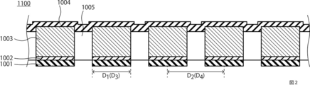
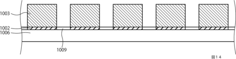
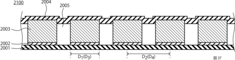
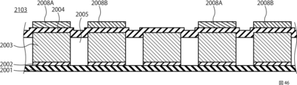
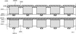
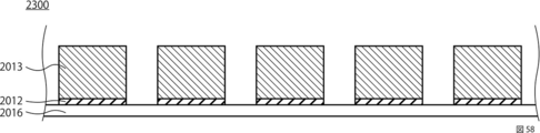
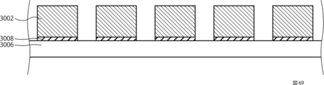
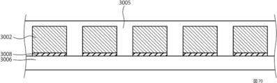
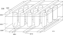
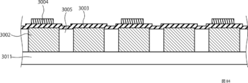
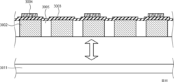
- FIG. 1 is a perspective view of the LED sheet 1100.
- FIG. 2 shows a cross-sectional view of the LED sheet 1100.
- the LED sheet 1100 includes a plurality of light emitting elements in which a first wiring 1001, a first buffer layer 1002, a light emitting layer 1003 including a diode, and a second wiring 1004 are sequentially stacked.
- An insulating layer 1005 is disposed.
- the first wiring 1001 extends in the first direction
- the second wiring 1004 extends in the second direction.
- the light emitting elements are uniformly arranged in the first direction and the second direction with the same size, but the size and arrangement of the light emitting elements are limited to the form shown in FIGS. It is not a thing.
- the LED sheet is used as a display device, it is preferable that the light emitting elements are arranged with a specific shape and pattern.
- the LED sheet 1100 can be used not only for a display device but also for a lighting device.
- the LED sheet 1100 has a first surface and a second surface opposite to the first surface, a plurality of light emitting elements having a light emitting layer 1003 including a diode, and an insulating layer 1005 disposed between the plurality of light emitting elements.
- the first wiring 1001 provided on the first surface side of the light emitting layer 1003 of the plurality of light emitting elements, and the second wiring 1004 provided on the second surface side of the light emitting layer 1003 of the plurality of light emitting elements.
- the LED sheet 1100 has a structure in which a light emitting element is disposed in an insulating layer 1005.
- the LED sheet can be made flexible. Flexible means that the LED sheet 1100 is not broken, chipped, or damaged by repeated winding and opening slowly 10 times on a cylindrical bar having a diameter of 200 mm under an atmospheric pressure environment of 25 ° C. Say.
- the LED sheet 1100 does not include a single crystal epitaxial growth substrate for growing the light emitting layer 1003 and is not used in manufacturing, the LED sheet 1100 can be manufactured at low cost.
- the LED sheet 1100 can be a passive matrix type that does not include a driving element (switching element) inside. Further, the LED sheet 1100 can be an active matrix type including a driving element therein.
- the switching element is not particularly limited, such as one or more selected from the group consisting of inorganic TFT (Thin Film Transistor) such as Si and IGZO, organic TFT, CMOS and diode.
- the active matrix LED sheet 1100 is also flexible. 1 and 2 show a passive matrix type LED sheet.
- the size of the LED sheet varies from several tens of mm 2 to more than 1 m 2 .
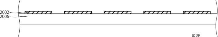
- the first wiring 1001 is a conductor that is in direct contact with the first buffer layer 1002.
- the first wiring 1001 is an electrode of each light emitting element.
- the first wiring 1001 serves as one of the anode and the cathode of the light emitting layer 1003.
- the first wiring 1001 is in direct contact with the first buffer layer 1002.
- the surface of the first buffer layer 1002 that is in contact with the first wiring 1001 is opposite to the surface of the first buffer layer 1002 that faces the second wiring 1004. It is preferable that the plurality of light emitting elements included in the LED sheet 1100 are electrically connected via the first wiring 1001.
- the first wiring 1001 includes either a metal film or a transparent conductive film.
- the first wiring 1001 can be a transparent electrode.
- the first wiring 1001 may be a laminated film.
- a metal film may be used for the first wiring 1001, and the first wiring 1001 may also function as a reflector.
- the first wiring 1001 may be able to electrically connect a plurality of light emitting elements arranged as shown in FIGS.
- the LED sheet 1100 is of an active matrix type
- one of the first wiring 1001 and the second wiring 1004 is connected to a driving element that selects a light emitting element that emits light.
- the LED sheet 1100 is an active matrix type
- one of the first wiring and the second wiring not connected to the driving element is a line-shaped, mesh-shaped, or film-shaped conductor, and a plurality of light-emitting elements Are electrically connected by a line, mesh, or film conductor.
- the first wiring 1001 includes a form that becomes an electrode of a light emitting element, a form that is a wiring connected to a driving element, a form that is an electrode of a driving element, and the like.
- the first buffer layer 1002 contains a layered compound.
- the first buffer layer 1002 is preferably plate-shaped.
- the first buffer layer 1002 is preferably a layer made of a layered compound.
- the first buffer layer 1002 is disposed between the first wiring 1001 and the light emitting layer 1003.
- the surface of the first buffer layer 1002 facing the light emitting layer 1003 is opposite to the surface of the first buffer layer 1002 facing the first wiring 1001.
- the first buffer layer 1002 is a single crystal containing a plurality of two-dimensional sheet-like layered compounds, or the crystal orientation of the surface facing the light emitting layer 1003 of the first buffer layer 1002 is uniform (the crystal orientation of the layered compound). is there.
- the crystallinity of the first buffer layer 1002 is determined by four-axis X-ray diffraction measurement or transmission electron microscope observation.
- a two-dimensional layered material such as graphene, a hexagonal metal such as hafnium or an alloy, or a ceramic may be used.
- the layered compound is a two-dimensional sheet extending in the surface direction of the first buffer layer 1002.
- a metal chalcogenide is preferable.
- graphene is also a layered compound, graphene cannot change the lattice constant according to the light emitting layer 1003.
- the lattice constant of the layered compound can be controlled by selecting the metal and the chalcogen element and the ratio thereof.
- a metal chalcogenide represented by MSe ⁇ S ⁇ Te ⁇ O ⁇ is preferable.
- M which is a metal contained in the metal chalcogenide is Ti, Zr, Hf, V, Nb, Ta, Cr, Mo, W, Zn, Cd, Ga, In, Ge, Sn, Pt, Au, Cu, Ag, Mn , Fe, Co, Ni, Pb, and Bi.
- ⁇ , ⁇ and ⁇ are 0.0 ⁇ ⁇ ⁇ 2.0, 0.0 ⁇ ⁇ ⁇ 2.0, 0.0 ⁇ ⁇ ⁇ 2.0, 0.0 ⁇ ⁇ ⁇ 2.0 and 1.0. It is preferable that ⁇ ⁇ + ⁇ + ⁇ + ⁇ ⁇ 2.0 is satisfied.
- ⁇ , ⁇ and ⁇ are 0.0 ⁇ ⁇ ⁇ 2.0, 0.0 ⁇ ⁇ ⁇ 2.0, 0.0 ⁇ ⁇ ⁇ 2.0, 0.0 ⁇ ⁇ ⁇ 2.0, 0 0.0 ⁇ + ⁇ + ⁇ and 1.0 ⁇ ⁇ + ⁇ + ⁇ + ⁇ ⁇ 2.0 are preferably satisfied.
- M which is a metal contained in the metal chalcogenide, preferably contains at least one selected from the group consisting of Mo, W, and Cr. The selection and ratio of metal chalcogenide elements are changed according to the light emitting layer 1003 to be epitaxially grown.
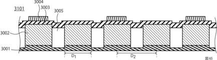
- the diameter (D1) of the first buffer layer 1002 is preferably in the range of 0.1 ⁇ m to 200 ⁇ m. Within this range, the light source is suitable for a display device.
- the diameter of the first buffer layer 1002 is determined as an inscribed circle diameter and a circumscribed circle diameter of each first buffer layer 1002 in a cross section perpendicular to the stacking direction of the light emitting elements. The average value of the determined inscribed circle diameter and circumscribed circle diameter is defined as the diameter of each first buffer layer.
- the diameter of the columnar body in which the first buffer layer 1002 and the light emitting layer 1003 are stacked depends on the diameter of the first buffer layer 1002.
- the diameter of the first buffer layer 1002 (columnar material) is preferably 1 ⁇ m or more and 200 ⁇ m or less. It is preferable that the cross-sectional area and the diameter of the first buffer layer 1002 are changed according to required luminance or the like.
- the plate shape (cross-sectional shape) of the first buffer layer 1002 is often a polygonal column shape such as a disc shape, a triangular column shape, or a hexagonal column shape, but may be any plate shape.
- the shapes of the adjacent first buffer layers 1002 may be different.
- the shortest distance (D2) between the centers of the first buffer layers 1002 (columnar objects) of the plurality of light emitting elements is 0.5 ⁇ m or more and 500 ⁇ m or less.
- a plurality of light emitting elements are included in the LED sheet 10. The plurality of light emitting elements are separated from each other, and there is a gap between the plurality of light emitting elements.
- the shortest distance between the centers of the first buffer layers 1002 of the plurality of light emitting elements is obtained as follows. First, the center point of the first buffer layer 1002 of one light emitting element and the center point of the first buffer layer 1002 of a plurality of light emitting elements around it are obtained.
- the shortest distance between the center point of the first buffer layer 1002 of one light emitting element and the center point of the first buffer layer 1002 of the plurality of light emitting elements on the outer periphery of the light emitting element is the distance between the plurality of light emitting elements.
- the shortest distance between the centers of the first buffer layers 1002 is used.
- the center point of the first buffer layer 1002 of the light emitting element is the center of the circumscribed circle of the first buffer layer 1002.
- the shortest distance between the centers of the first buffer layers 1002 (columnar objects) of the plurality of light emitting elements is more preferably 5 ⁇ m to 300 ⁇ m, and more preferably 30 ⁇ m to 100 ⁇ m.
- the number of pixels of the shortest distance product between the centers of the first buffer layers 1002 of the plurality of light emitting elements is changed.
- the thickness of the first buffer layer 1002 is not particularly limited.
- the thickness of the first buffer layer 1002 is, for example, not less than 10 nm and not more than 1000 nm.
- the variation in the thickness of the first buffer layer 1002 is preferably as small as possible.
- the first buffer layer 1002 and the light emitting layer 1003 are in a heteroepitaxial relationship.
- the stacking direction of the light emitting elements is parallel to the hexagonal c-axis of the metal chalcogenide.
- the metal chalcogenide perpendicular to the stacking direction of the light emitting elements is parallel to the hexagonal a and b axes.
- the orientation of the metal chalcogenide parallel to the substrate surface is random and is not particularly limited as viewed perpendicularly from the substrate surface.
- the metal chalcogenide can arbitrarily change the lattice constant by selecting the element, the lattice constant of the single crystal layer to be epitaxially grown and the lattice constant of the metal chalcogenide can be matched by changing the composition of the metal chalcogenide. That is, by changing the composition of the metal chalcogenide according to the single crystal layer to be epitaxially grown and the crystal orientation to be grown, for example, a substrate suitable for epitaxial growth such as GaN, InN, and AlN can be prepared. In these hexagonal nitrides, the plane orientation for growth is the 0001 direction.
- the difference between the in-plane lattice constant of the first buffer layer 1002 and the in-plane lattice constant of the layer that is closest to the first buffer layer 1002 among the light emitting layers 1003 in which a plurality of layers are stacked ([[the first buffer layer 1002 of In-plane lattice constant]-[in-plane lattice constant of the light emitting layer 1003 closest to the first buffer layer 1002] / [in-plane lattice constant of the first buffer layer 1002]) within ⁇ 1%
- the difference in lattice constant is large, epitaxial growth is difficult, and if the deviation is large, epitaxial growth does not occur or crystal defects are likely to occur, so that the in-plane lattice constant of the first buffer layer 1002 and a plurality of layers are easily formed.
- the difference in the in-plane lattice constant of the layer present on the first buffer layer 1002 side of the light emitting layer 1003 in which is stacked is within ⁇ 0.5%.
- the child constant is obtained by four-axis X-ray diffraction measurement, or is generally determined by the composition ratio of the metal chalcogenide constituting the first buffer layer 1002.
- MoS 1.6 Se 0.4 is used, and the error between the GaN a-axis length 3.189 mm and the metal chalcogenide a-axis length 3.189 mm is 0.0%, which is suitable for epitaxial growth of GaN. It is.
- the two-dimensional sheet-shaped metal chalcogenide that is in direct contact with the light emitting layer 1003 of the first buffer layer 1002 may be composed of a plurality of two-dimensional sheet-shaped metal chalcogenides.
- the surface of the first buffer layer 1002 that is in direct contact with the light emitting layer 1003 is arranged so that the crystal orientations of the plurality of two-dimensional sheet-shaped metal chalcogenides are aligned.
- a plurality of two-dimensional sheet-shaped metal chalcogenides may be overlapped, and there may be a step.
- the surface of the first buffer layer 1002 that is in direct contact with the light emitting layer 1003 is not a metal chalcogenide of a single two-dimensional sheet at the time of peeling from the substrate used at the time of manufacturing, a plurality of two-dimensional sheets of If the crystal orientation of the metal chalcogenide is uniform, the light emitting layer 1003 can be epitaxially grown on the first buffer layer 1002. Since epitaxial growth is possible even if it is not a perfect sheet, a member in which a plurality of first buffer layers 1002 are arranged on a substrate can be manufactured at low cost. And the production cost of an LED sheet can be suppressed by producing an LED sheet using the board
- the light emitting layer 1003 is a light emitting diode disposed between the first buffer layer 1002 and the second wiring 1004.
- the light emitting layer 1003 is in direct contact with the first buffer layer 1002 and in direct contact with the second wiring 1004.
- the surface in which the light emitting layer 1003 is in direct contact with the second wiring 1004 is opposite to the surface in direct contact with the first buffer layer 1002.
- the light emitting layer 1003 includes a first conductivity type semiconductor layer (compound semiconductor layer), an active layer, and a second conductivity type semiconductor layer (compound semiconductor layer).
- the light emitting layer 1003 includes a hexagonal nitride semiconductor layer.
- the light-emitting layer 1003 is preferably formed by stacking a plurality of hexagonal nitride semiconductor layers.
- the plurality of layers of the light emitting layer 1003 are preferably in a heteroepitaxial relationship. That is, a quantum well structure that improves the luminous efficiency is included.
- the nitride semiconductor layer is preferably a single crystal layer of GaN, InN, AlN, and two or more mixed compositions selected from the group consisting of GaN, InN, and AlN.
- the in-plane lattice constant of the nitride semiconductor layer has a width from 3.111 to 3.532.
- the metal chalcogenide composition ratio may be slightly changed in consideration of the difference in thermal expansion coefficient during film formation and the growth rate.
- Compound semiconductors (including active layers) used for the light emitting layer 1003 include GaN, InN, AlN, and two or more mixed compositions selected from the group consisting of GaN, InN, and AlN, as well as GaAs.
- Examples include arsenic compound semiconductors and phosphorus compound semiconductors such as InGaAlP.
- the arsenic compound semiconductor and the phosphorus compound semiconductor can have the same in-plane lattice constant with the first buffer layer 1002 as in the case of the nitride semiconductor.
- An arsenic compound semiconductor or a phosphorus compound semiconductor can be preferably grown as the light emitting layer 1003 from the first buffer layer 1002. That is, the first conductivity type semiconductor layer, the active layer, and the second conductivity type semiconductor layer are semiconductor layers including at least one selected from the group consisting of nitride semiconductors, arsenic compound semiconductors, and phosphorus compound semiconductors. .
- the light emitting layer 1003 When the light emitting layer 1003 is a blue light emitting diode, the light emitting layer 1003 includes, for example, a first conductivity type GaN, a first conductivity type AlGaN, an InGaN, a second conductivity type AlGaN, and a second conductivity type GaN.
- the in-plane lattice constant of the first buffer layer 1002 is set to GaN.
- MoS 1.6 Se 0.4 for the metal chalcogenide, the lattice constants of the metal chalcogenide and GaN are matched.
- the diameter (D3) of the light emitting layer 1003 is preferably in the range of 0.1 ⁇ m or more and 200 ⁇ m or less. Within this range, the light source is suitable for a display device. Regarding the diameter of the light emitting layer 1003, the inscribed circle diameter and the circumscribed circle diameter of the light emitting layer 1003 are obtained in a cross section perpendicular to the stacking direction of the light emitting elements. The average value of the obtained inscribed circle diameter and circumscribed circle diameter is defined as the diameter of each light emitting layer 1003.
- the diameter of the columnar body in which the first buffer layer 1002 and the light emitting layer 1003 are stacked is affected by the diameter of the first buffer layer 1002.
- the diameter of the light emitting layer 1003 (columnar material) is preferably 1 ⁇ m or more and 200 ⁇ m or less.
- the cross-sectional area and diameter of the light emitting layer 1003 are preferably changed according to required luminance or the like.
- the cross-sectional shape of the light emitting layer 1003 is often a polygonal prism shape such as a disc shape, a triangular prism shape, or a hexagonal prism shape, but is not particularly limited.
- the shapes of the adjacent light emitting layers 1003 may be different.
- the shortest distance (D4) between the centers of the light emitting layers 1003 of the plurality of light emitting elements is 0.5 ⁇ m or more and 500 ⁇ m or less.
- a plurality of light emitting elements are included in the LED sheet 1100. The plurality of light emitting elements are separated from each other, and there is a gap between the plurality of light emitting elements.
- the shortest distance between the centers of the light emitting layers 1003 of the plurality of light emitting elements is obtained as follows. First, the center point of the light emitting layer 1003 of one light emitting element and the center point of the light emitting layer 1003 of a plurality of light emitting elements around it are obtained.
- the shortest distance between the center point of the light emitting layer 1003 of one light emitting element and the center point of the light emitting layer 1003 of the plurality of light emitting elements on the outer periphery of the light emitting element is the light emitting layer 1003 of the plurality of light emitting elements.
- the center point of the light emitting layer 1003 of the light emitting element is the center of the circumscribed circle of the light emitting layer 1003.
- the shortest distance between the centers of the light emitting layers 1003 of the plurality of light emitting elements is more preferably 5 ⁇ m to 300 ⁇ m, and 30 ⁇ m to 100 ⁇ m.
- the number of pixels of the shortest distance product between the centers of the light emitting layers 1003 of the plurality of light emitting elements is changed.
- the second wiring 1004 is a conductor that is in direct contact with the light emitting layer 1003.
- the second wiring 2 is an electrode of each light emitting element. It is preferable that the plurality of light emitting elements included in the LED sheet 1100 are electrically connected via the second wiring 1004.
- the second wiring 1004 includes either a metal film or a transparent conductive film.
- the second wiring 1004 can be a transparent electrode.
- the second wiring 1004 may be a laminated film.
- a metal film may be used for the second wiring 1004, and the second wiring 1004 may also function as a reflector.
- the second wiring 1004 includes a form that becomes an electrode of a light emitting element, a form that is a wiring connected to the driving element, a form that is an electrode of the driving element, and the like.
- the insulating layer 1005 is disposed between the plurality of light emitting elements.
- the insulating layer 1005 preferably holds the light emitting element and becomes a base of the LED sheet 1100.
- the insulating layer 1005 is made of an insulating material containing a polymer.
- the surface of the insulating layer 1005 facing the light emitting element is in direct contact with at least part of the surface of the light emitting element facing the insulating layer 1005 (side surface of the light emitting element).
- the surface of the insulating layer 1005 facing the light emitting element includes a direction perpendicular to the stacking direction of the light emitting elements.
- the insulating layer 1005 is in direct contact with the first buffer layer 1002, the light emitting layer 1003, or the side surfaces of the first buffer layer 1002 and the light emitting layer 1003.
- the insulating layer 1005 is filled between the light emitting layers 1003 grown in a columnar shape and spreads in a sheet shape.
- the insulating layer 1005 is a polymer spacer.
- the thickness of the insulating layer 1005 is such that it covers the first buffer layer 1002 and the light emitting layer 1003 grown thereon.
- the insulating layer having a thickness of about 2 to 5 ⁇ m insulates the light emitting layer, It is a part that bears the flexibility of the light-emitting element sheet and the display sheet as products, and it is preferable to select a material based on strength and workability.
- a colored or colorless polymer can be used as the insulating layer 1005. From the viewpoint of reducing light absorption loss, a colorless and transparent one is more desirable.
- the polymer that can be used as the insulating layer 1005 include a fluororesin, an epoxy resin, and a silicon resin.
- the insulating layer 1005 is filled with, for example, a fluorine resin, a transparent resin, a transparent polymer, or the like at least between a plurality of light emitting layers including a diode. Specifically, at least a part of the side surface of the light emitting layer 1003 is covered, and at least filled between the plurality of light emitting layers so that the plurality of light emitting layers 1003 do not directly contact each other. More specifically, in the case where the first wiring 1001 and the second wiring 1004 are also formed on part of the side surface of the light emitting layer 1003, the insulating layer 1005 is also formed on the outer peripheral side surface of the first wiring 1001 and the second wiring 1004. May be formed.
- an insulating layer 1005 is formed on the surface where the light emitting layer 1003 which is the upper end surface of the light emitting layer 1003 is in contact with the first wiring 1001 and the surface where the light emitting layer 1003 which is the lower end surface is in contact with the second wiring 1004.
- the insulating layer 1005 may cover a part of the side surfaces of the first wiring 1001 and the second wiring 1004, but the surface opposite to the surface facing the light emitting layer 1003 of the first wiring 1001.
- the insulating layer 1005 is preferably not formed on the surface of the second wiring 1004 opposite to the surface facing the light emitting layer 1003.
- the insulating layer 1005 is in contact with the light emitting layer 1003.
- the light emitted from the light emitting layer 1003 is totally reflected on the surface in contact with the insulating layer 1005, color mixture of pixels can be prevented.
- the light emitting elements 1003 are densely arranged, the interval between the light emitting elements is narrowed and the color mixture between the pixels is likely to occur.
- the material which increases the refractive index difference between the light emitting layer 1003 and the insulating layer 1005 is insulated. By selecting the layer 1005, color mixture between pixels can be prevented.
- the refractive index n 3 of the light emitting layer 1003 is approximately 3.0, specifically 2.4 to 2.5, and the same numerical values as other nitride semiconductor layers, The details are close to 1.9 to 2.9.
- the refractive index of the light-emitting layer 1003 is around 2.4 to 2.5, it is preferable to select a material for the insulating layer 1005 that is smaller than the refractive index n 3 of the light-emitting layer 3.
- the refractive index n 5 of the insulating layer 1005 is less than 2.5, preferably less than 1.9, more preferably less than 1.5.
- the refractive index difference between the insulating layer 1005 and the light emitting layer 1003 is very large, preventing color mixture between pixels, and further the light emission intensity of the LED sheet 1100. It is very preferable in that it becomes high.
- the light emission 1002 is epitaxially grown on the first buffer layer 1002.
- a light emitting layer 1003 in which an n-type GaN layer, a superlattice (Strained-Layer ⁇ Superlattice; SLS), a multi-quantum well (MQW) as an active layer, and a p-type GaN layer are stacked will be described as an example.
- SLS relaxed-Layer ⁇ Superlattice
- MQW multi-quantum well
- n-type GaN is grown on the first buffer layer 1002.
- the growth of the n-type GaN layer is preferably performed by supplying a nitrogen gas as a carrier gas, in which the first buffer layer 1002 is not easily destroyed.
- a nitrogen gas as a carrier gas
- the n-type impurity one or more selected from the group consisting of Si, Ge, Te and Sn is used.
- the size and shape of the ground plane with the n-type GaN first buffer layer 1002 are controlled by the shape of the first buffer layer 1002.
- the height of the n-type GaN layer is typically about several ⁇ m, and is controlled to be the designed height.
- the first buffer layer 1002 is selected so that the (0001) plane of the n-type GaN layer grows.
- the n-type GaN layer may be further grown using a mixed gas of nitrogen gas and hydrogen gas or hydrogen gas as a carrier gas from the viewpoint of growth control and the like.
- a mixed gas of nitrogen gas and hydrogen gas or hydrogen gas as a carrier gas from the viewpoint of growth control and the like.
- the (0001) plane which is a polar plane, but also a semipolar plane such as the (10-11) plane and a non-polar plane such as the (1-100) plane Polar faces may be mixed.
- the internal electric field due to polarization may be reduced and the droop phenomenon may be suppressed.
- the n-type GaN layer on the superlattice or multiple quantum well side may be thicker than the first buffer layer 1002. Note that the emission spectrum can be controlled by the cross-sectional diameter of the light-emitting layer 1003.
- a stacked structure in which, for example, a plurality of 2 nm n-type GaN and 1 nm InGaN (In ⁇ Ga) are periodically stacked as superlattices is formed on the nGaN layer.
- the superlattice may be omitted.
- Multiple quantum wells are formed on the superlattice or n-type GaN layer.
- the multiple quantum well has a structure in which a plurality of barrier layers (non-doped GaN) layers and well layers (InGaN) layers are stacked.
- An example of the stack of multiple quantum wells is a structure in which 10 or less pairs of InGaN and GaN are stacked (for example, 8 pairs in the case of blue light emission).
- the thickness of each layer of the multiple quantum well is several nm.
- the emission spectrum can be controlled by changing the composition of In or Al in the well layer.
- a p-type GaN layer is grown on the multiple quantum well.
- the p-type impurity one or more selected from the group consisting of Mg and Zn is used.
- the p-type GaN layer has a single layer structure or a laminated structure.
- the thickness of the p-type GaN layer is, for example, about 150 nm.
- On the surface of the p-type GaN layer not only the (0001) plane but also a semipolar plane such as the (10-11) plane as with the surface of the n-type GaN layer And nonpolar surfaces such as (1-100) surfaces may be mixed.
- the thickness of the p-type GaN layer can be controlled in the same manner as the n-type GaN layer.
- the n-type GaN of the light emitting layer 1003 manufactured by such a method is in contact with the first wiring 1001 and the p-type GaN is in contact with the second wiring 1004.
- the diameter of the light emitting layer 1003 (the diameter of the inscribed circle of the columnar object) can be changed. At this time, the diameter of the light emitting layer 1003 on the first wiring 1001 side is different from the diameter on the second wiring side 1004 side.
- the method for producing the LED sheet 1100 described below includes a step (first step) of forming a plurality of first buffer layer precursors in a plate shape (dot shape) on a non-oriented substrate, and a first buffer layer precursor.
- Heating a member formed on the non-oriented substrate to form a plurality of first buffer layers containing the layered compound on the non-oriented substrate (second step), and a plurality of first A step of forming a plurality of pillars by epitaxially growing a light emitting layer on the buffer layer (third step), a step of forming an insulating layer filling between the plurality of pillars (fourth step), and a plurality of pillars; A step of forming a second wiring on a surface of the light emitting layer opposite to the surface facing the first buffer layer (fifth step), a non-oriented substrate is peeled off, and a plurality of columnar objects are formed.
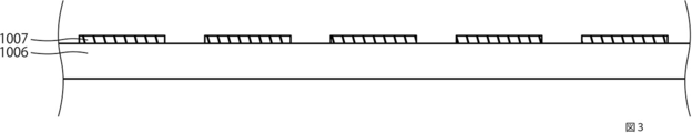
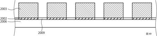
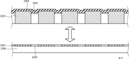
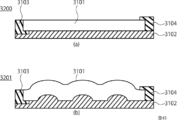
- FIG. 3 shows a step (first step) of forming a plurality of first buffer layer precursors 1007 on the non-oriented substrate 1006 in a plate shape.
- the non-oriented substrate 1006 may be anything as long as there is no crystal orientation that is uniquely determined over the entire surface of the substrate, such as glass, metal, polycrystal, plastic (resin), ceramics, and amorphous.
- the non-oriented substrate 1006 is not particularly limited as long as it holds the first buffer layer 1002 necessary for epitaxial growth. It is not necessary to use an expensive single crystal base material for the non-oriented substrate 1006. Further, the non-oriented substrate 1006 is not included in the light emitting element.
- the first buffer layer precursor 1007 is obtained by forming a metal contained in a layered compound into a plate shape.
- the first buffer layer precursor 1007 that is a metal (or alloy) is formed in a plate shape by forming and patterning a metal film (or alloy film).
- the first buffer layer precursor 1007 includes Ti, Zr, Hf, V, Nb, Ta, Cr, Mo, W, Zn, Cd, Ga, In, Ge, Sn, Pt, Au, Cu, Ag, Mn, and Fe.
- the metal of the first buffer layer precursor 1007 is selected according to the light emitting layer 1003 to be epitaxially grown.
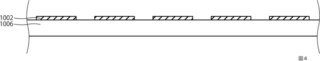
- a member in which the first buffer layer precursor 1007 is formed on the non-oriented substrate 1006 is heated to form a plurality of first buffer layers 1002 including a layered compound on the non-oriented substrate 1006 in a plate shape.
- the process (2nd process) formed in is shown.
- the heating is performed in an atmosphere containing one or more selected from the group consisting of Se, S, Te, and O (oxygen).
- the first buffer layer 1002 is formed on the non-oriented substrate 1006.
- Heating conditions are selected according to the light emitting layer 1003 to be epitaxially grown. It is preferable that all the plate-like first buffer layers 1002 have the same composition.
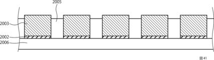
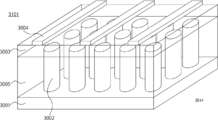
- FIG. 5 shows a step (third step) in which the light emitting layer 1003 is epitaxially grown on the plurality of first buffer layers 1002 to form a plurality of columnar objects.
- the columnar body includes one first buffer layer 1002 and a light emitting layer 1003 formed on the first buffer layer 1002. Since the lattice constant of the first buffer layer 1002 matches the lattice constant of the layer to be epitaxially grown, the light emitting layer 1003 grows epitaxially on the first buffer layer 1002. Since the growth hardly occurs on the non-oriented substrate 1006, the light emitting layer 1003 is selectively grown on the first buffer layer 1002.
- the light emitting layer 1003 includes a plurality of layers such as an electrode contact layer and a quantum well, epitaxial growth is performed a plurality of times, and the light emitting layer 1003 is epitaxially grown on the plurality of first buffer layers 1002 to form a plurality of columnar objects.
- FIG. 6 shows a step (fourth step) of forming an insulating layer 1005 filling between a plurality of columnar objects.
- An insulating layer 1005 is formed so as to fill a space between the columnar members of a member in which a plurality of columnar materials are formed on the non-oriented substrate 1006.
- the insulating layer 1005 can be formed by dipping, spraying, spin coating, or the like.
- the insulating layer 1005 may expose a part of the columnar object on the side opposite to the non-oriented substrate 1006 side, or the columnar object may be completely covered. If necessary, since the light emitting layer 1003 is in direct contact with the second wiring 1004, part of the insulating layer 1005 can be removed to expose at least part of the surface of the light emitting layer 1003.
- FIG. 7 shows a step (fifth step) of forming the second wiring 1004 on the surface opposite to the surface facing the plurality of first buffer layers 1002 of the plurality of columnar light emitting layers 1003. This step may be performed after the non-oriented substrate 1006 is peeled off.
- a conductive second wiring 1004 is formed over the light emitting layer 1003. This wiring may be a wiring that connects the light emitting elements arranged side by side, or may be a wiring that is connected to a driving element. In FIG. 7, the second wiring 1004 is formed so as to connect the light emitting elements arranged in the horizontal direction.
- FIG. 8 shows a step of peeling the non-oriented substrate 1006. Then, by forming the first wiring 1001 so as to be in direct contact with the lower side of the first buffer layer 1002 (the surface opposite to the surface facing the light emitting layer 1003 of the first buffer layer 1002), FIG. The LED sheet 1100 shown in the cross-sectional view is obtained.
- This wiring may be a wiring connecting the light emitting elements arranged side by side or a wiring connecting to the driving element.
- the second wiring 1004 is formed so as to connect the light emitting elements arranged in the depth direction of FIG.
- the second wiring 1004 side is preferably fixed to a base material (not shown) and peeled off. Since the first buffer layer 1002 is fixed to the non-oriented substrate 1006 by van der Waals contact, the first buffer layer 1002 is physically easily peeled off. By peeling off the insulating layer 1005, the light emitting element portion including the light emitting layer 1003 epitaxially grown with the first buffer layer 1002 is attached to the sheet side of the insulating layer 1005. At this time, a part of the layered compound may be peeled off. The first buffer layer 1002 remaining on the sheet side may be intentionally peeled off by electrostatic adsorption, ultrasonic treatment, cleaning, etching, or the like.
- the LED sheet 1100 can be manufactured without using a very expensive single crystal substrate, the manufacturing cost is lower than when the single crystal substrate is used or manufactured. Significant reduction is achieved. In addition, it is possible to increase the film forming area, which is limited by the wafer shape of the single crystal substrate, and to improve the shape flexibility such as a square shape, which also leads to cost reduction and design flexibility.
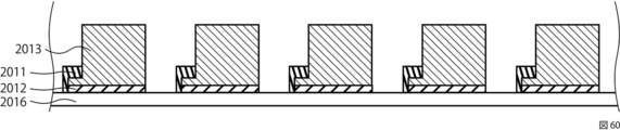
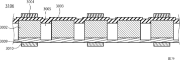
- the second embodiment relates to an LED sheet.
- the LED sheet of the second embodiment is a modification of the first embodiment.
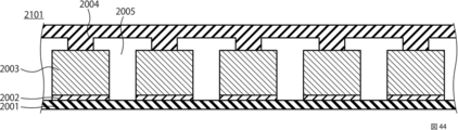
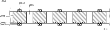
- FIG. 9 shows a cross-sectional view of the LED sheet 1101.
- the LED sheet 1101 includes a plurality of light emitting elements in which a first wiring 1001, a first buffer layer 1002, a light emitting layer 1003 including a diode, and a second wiring 1004 are sequentially stacked.
- An insulating layer 1005 is disposed.
- common description is omitted.
- the difference between the LED sheet 1101 and the LED sheet 1100 is that the insulating layer 1005 is also formed on a part of the surface of the light emitting layer 1003 in contact with the second wiring 1004.
- the second wiring 1004 is in direct contact with the light emitting layer 1003 from between the insulating layers 1005 above the light emitting layer 1003.
- the third embodiment relates to an LED sheet.
- the LED sheet of the third embodiment is a modification of the first embodiment.
- FIG. 10 shows a cross-sectional view of the LED sheet 1102.
- the LED sheet 1101 includes a plurality of light emitting elements in which a first wiring 1001, a first buffer layer 1002, a light emitting layer 1003 including a diode, and a second wiring 1004 are sequentially stacked.
- An insulating layer 1005 is disposed.
- a common description is omitted.
- the difference between the LED sheet 1101 and the LED sheet 1100 is that the second wiring 1004 side of the light emitting layer 1003 has a conical shape.
- the second wiring 1004 is along the cone shape of the light emitting layer 1003.
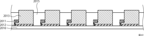
- the fourth embodiment relates to an LED sheet.
- the LED sheet of the fourth embodiment is a modification of the first embodiment.
- FIG. 11 shows a cross-sectional view of the LED sheet 1101.
- the LED sheet 1101 includes a plurality of light emitting elements in which a first wiring 1001, a first buffer layer 1002, a light emitting layer 1003 including a diode, and a second wiring 1004 are sequentially stacked.
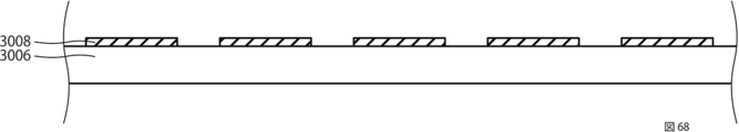
- An insulating layer 1005 is provided, and a transmissive color gamut adjusting layer 1008 is formed over at least part of the light emitting elements.
- a common description is omitted.
- the transmission color gamut adjustment layer 1008 is a phosphor, a color filter, a quantum dot, or a phosphor and a color filter.
- FIG. 11 shows an example of an LED sheet capable of full color display when the light emitting element emits blue light.
- a green phosphor 1008A and a red phosphor 1008B are arranged on the second wiring 1004 for the two light emitting elements, and one light emitting element has a fluorescent light. Neither body nor color filter is placed.
- the emission intensity changes by providing the green phosphor 1008A or the red phosphor 1008B for example, by changing the area of the light emitting element for each color to emit light
- full color display including white can be performed.
- a transmission color gamut adjustment layer 1008 is provided on both sides of the first wiring 1001 and the second wiring 1004.
- a transmission color gamut adjusting layer 1008 is provided on the light emitting surface side.
- the transmission color gamut adjustment layer 1008 is formed by vapor deposition, ink jet, or the like.
- the fifth embodiment relates to an LED sheet.
- the LED sheet of the fifth embodiment is a modification of the first embodiment.
- the LED sheet of the fifth embodiment includes at least a first wiring, a light emitting layer including a diode, a plurality of light emitting elements in which second wirings are sequentially stacked, and an insulating layer arranged between the plurality of light emitting elements.
- the light emitting layer is in direct contact with the first wiring, and the surface of the light emitting layer opposite to the surface in direct contact with the first wiring is in direct contact with the second wiring.
- common description is omitted.
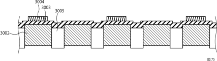
- FIG. 12A shows a cross-sectional view of the LED sheet 1104 of the fifth embodiment.
- the first buffer layer 1002 is not included, and the light emitting layer 1003 is similar to the LED sheet of the first embodiment except that the light emitting layer 1003 is in direct contact with both the first wiring 1001 and the second wiring 1004. Since the first buffer layer 1002 is conductive, it may be included between the light emitting layer 1003 and the first wiring 1001, but the first buffer layer 1002 can be omitted.
- the surface of the light emitting layer 1003 opposite to the surface directly in contact with the first wiring 1001 is in direct contact with the second wiring 1004. Since the first buffer layer 1002 easily absorbs light, it is preferable that the light emission efficiency is improved by removing the layered compound.
- the LED sheet 1104 has a first surface and a second surface opposite to the first surface, and includes a plurality of light emitting elements having a light emitting layer 1003 including a diode, and an insulating layer 1005 disposed between the plurality of light emitting elements.
- a first wiring 1001 provided in contact with the first surface of the light emitting layer 1003 of the plurality of light emitting elements, and a second wiring 1004 provided in contact with the second surface of the light emitting layer 1003 of the plurality of light emitting elements.
- the LED sheet 1104 is produced by a step of forming a plurality of first buffer layer precursors on a non-oriented substrate (seventh step), and the formation of the first buffer layer precursor on the non-oriented substrate.
- Heating the formed member to form a plurality of buffer layers containing a layered compound on a non-oriented substrate in a plate shape (eighth step), and epitaxially growing a light emitting layer on the plurality of first buffer layers A step of forming a plurality of pillars (a ninth step), a step of forming an insulating layer filling between the plurality of pillars (a tenth step), and a surface having a layered compound of the plurality of pillars
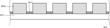
- substrate 1006 and the 1st buffer layer 1002 differs from the preparation methods in 1st Embodiment.
- the method for peeling the first buffer layer 1002 is not limited, but, for example, after the non-oriented substrate 1006 is peeled off, the first buffer layer 1002 may be peeled off by electrostatic adsorption, ultrasonic waves, tape adsorption peeling, etching, washing, or the like.
- a method of forming an insulating material, fixing the first buffer layer 1002, and peeling the first buffer layer 1002 together with the insulating material before epitaxial growth will be described with reference to FIGS.
- a step (seventh step) of forming a plurality of first buffer layer precursors in a plate shape on a non-oriented substrate 1006, and a member in which the first buffer layer precursor is formed on the non-oriented substrate are heated.
- a step (eighth step) of forming a plurality of first buffer layers containing a layered compound in a plate shape on a non-oriented substrate is performed.
- a resist is formed by the photolithography so that the plate-like first buffer layer 1002 is partially exposed.
- an insulating film 1009 is formed between the first buffer layers 1002 as shown in FIG.
- the insulating film 1009 is formed of, for example, SiO 2 by sputtering.
- the resist is removed by lift-off, and a part of the plate-like first buffer layer 1002 is exposed.
- the first buffer layer 1002 can be removed without using the insulating film 1009.
- the process (9th process) which carries out the epitaxial growth of the light emitting layer 1003 on the some 1st buffer layer 1002, and forms a some columnar thing is performed.
- the step of forming the insulating layer 1005 filling the space between the plurality of pillars (the tenth step) is opposite to the surface of the plurality of pillars 3 having the first buffer layer 1002.
- a step of forming the second wiring on the side surface (11th step) is performed.
- substrate 1006 and the 1st buffer layer 1002 is performed.
- the first buffer layer 1002 fixed by the insulating film 1009 together with the non-oriented substrate 1006 may be peeled off, or may be peeled off separately.
- a step of forming the first wiring 1001 on one surface in a direction perpendicular to the surface of the plurality of columnar objects facing the insulating layer 1005 is performed to obtain the LED sheet 1104 of FIG.
- FIG. 12B shows another LED sheet 1004 ′ that does not include the first buffer layer 1002.
- the diameter of the light emitting layer 1003 on the first wiring 1001 side is thin, and the diameter of the light emitting layer 1003 n on the second wiring 1004 side is large.
- the light emitting layer 1003 is easily caught by the insulating layer 1005 and is difficult to come off between the insulating layers 1005 when being separated from the non-oriented substrate 1006. There is a case.
- the light emitting layer 1003 is provided on the non-oriented substrate 1006 side after peeling, the voids that have escaped from between the insulating layers 1005 become the dots of the LED sheet.
- the diameter of the light emitting layer 1003 is controlled, the adhesion between the light emitting layer 1003 and the insulating layer 1005 is improved, and the non-oriented substrate 1006 is easily peeled. .
- an adhesive may be provided between the light emitting layer 1003 and the insulating layer 1005.
- the adhesive is handled as a material included in the insulating layer 1005.
- the adhesive is not limited as long as the light emitting layer 1003 is difficult to come off from the insulating layer 1005.
- a plurality of means for preventing dot omission of the LED sheet can be combined.
- ⁇ Molecular bonding agent can also be used as an example of an adhesive that prevents missing dots on the LED sheet.
- the molecular bonding agent prevents the light emitting layer 1003 from coming off the insulating layer 1005 by increasing the adhesion between the side surface of the light emitting layer 1003 and the insulating layer 1005.
- a molecular bonding agent is applied to the side surface of the light emitting layer 1003 so as not to adhere to the non-oriented substrate 1006, and then the insulating layer 1005 is formed, and the light emitting layer 1003 and the insulating layer 1005 are bonded.
- a small amount of the insulating layer 1005 is applied to the side surface of the light emitting layer 1003, and then a molecular bonding agent is applied.
- the insulating layer 1005 is further applied to increase the adhesion between the side surface side of the light emitting layer 1003 and the insulating layer 1005. Can be increased.
- adhesion between the non-oriented substrate 1006 and the insulating layer 1005 can be improved.
- the adhesive it is preferable to select a suitable material according to the material to be bonded.
- the insulating film 1009 provided between the insulating layer 1005 and the non-oriented substrate 1006 has low adhesiveness to the non-oriented substrate 1006.
- a material having high adhesiveness can be selected.
- a layer or a film other than the insulating film 1009 may be formed.
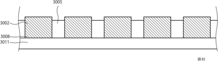
- the sixth embodiment relates to an LED sheet.
- the LED sheet of the sixth embodiment is a modification of the first embodiment.
- FIG. 17 shows a cross-sectional view of the LED sheet 1105.
- the LED sheet 1105 includes a plurality of light emitting elements in which a first wiring 1001, a first buffer layer 1002, a light emitting layer 1003 including a diode, and a second wiring 1004 are sequentially stacked.
- An insulating layer 1005 is disposed and includes a driving element 1010 electrically connected to the first wiring 1001. In the first embodiment 1 and the sixth embodiment, common description is omitted.
- a driving element 1010 such as a TFT is formed in an individual light emitting element, and the light emission on / off of the element can be driven by the TFT.
- the light emitting elements can be individually turned on / off by forming the wiring in a stripe shape so that the first wiring 1001 and the second wiring 1004 intersect.
- the seventh embodiment relates to an LED sheet.
- the LED sheet of the seventh embodiment is a modification of the first embodiment.
- FIG. 18 shows a cross-sectional view of the LED sheet 1106.
- the LED sheet 1106 includes a plurality of light emitting elements in which a first wiring 1001, a first buffer layer 1002, a light emitting layer 1003 including a diode, and a second wiring 1004 are sequentially stacked.
- An insulating layer 1005 is disposed and includes a driving element 1010 electrically connected to the second wiring 1004.
- the first embodiment and the sixth embodiment are common except that the drive element 1010 is connected to the second wiring 1004.
- Each of the LED sheets shown in the first to seventh embodiments has a structure that can be manufactured without using a single crystal substrate that is expensive and has limited size and shape, and is a practical LED. It is a sheet. Moreover, these LED sheets are also suitable in that they can be used for display devices and lighting devices in which the light emitting portion can be bent by making them flexible. The LED sheet can be used for displays such as televisions and smartphones. In addition, it can be used for wallpaper, clothing, and flexible displays for bent parts.
- the eighth embodiment is a display device using the LED sheet of the embodiment.
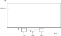
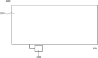
- FIG. 19 shows a conceptual diagram of the display device 1200.
- the display device 1200 includes an LED sheet 1201, a control unit 1202, a power supply unit 1203, and a signal input unit 1204.
- Display device 1200 may be housed in one housing or may be divided into a plurality of housings.
- the LED sheet 1201 is preferably not weathered, but is sealed with a polymer material, a resin material, a glass material, or the like, and has weather resistance.
- the LED sheet 1201 may not be accommodated in the housing as long as the LED sheet 1201 includes a light emitting element control terminal.
- the LED sheet 1201, the control unit 1202, the power supply unit 1203, and the signal input unit 1204 constituting the display device 1200 are connected by wire, wireless, or wired and wireless.
- the LED sheet 1201 controls light emission, non-light emission, light emission intensity, and the like of a specific light emitting element by a signal and power from the control unit 1202.
- the control unit 1202 may process an image signal to be displayed on the LED sheet 1201.
- the signal input to the signal input unit 1204 is processed by the control unit 1202.
- the signal input unit 1204 can have a function of processing an external signal and a communication function such as a tuner.
- the control unit 1202 may be connected to one part of the LED sheet 1201 or may be connected to a plurality of LED sheets 1201.
- the power supply unit 1203 is connected to the control unit 1202 and the signal input unit 1204, and converts the power into power necessary for operating the display device 1200.
- the power supply unit 1203 includes, for example, an AC-DC converter and a DC-DC converter.
- a non-flexible LED sheet with a support that is held on the support by a process of holding on the support can be used.
- the ninth embodiment relates to an LED sheet.
- the LED sheet of the ninth embodiment includes a non-oriented substrate, a first wiring, a second buffer layer, a light emitting layer, a second wiring, and an insulating layer.
- the light emitting layer is disposed between the second buffer layer and the second wiring.
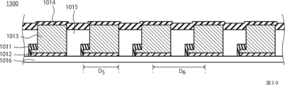
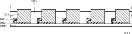
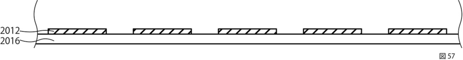
- FIG. 20 shows a cross-sectional view of the LED sheet 1300 of the ninth embodiment.
- An LED sheet 1300 illustrated in FIG. 20 includes a non-oriented substrate 1016 and a plurality of light-emitting elements on the non-oriented substrate 1016, and an insulating layer is disposed between the plurality of light-emitting elements.
- the light emitting layer includes a plurality of layers.
- the light emitting layer 1013 has an extending surface on the second buffer layer 1012 side, and the extending surface is in direct contact with the first wiring 1011. In addition, the extending surface is disposed between the first wiring 1011 and the second buffer layer 1012.
- the light emitting element of the LED sheet 1300 has a horizontal device structure.
- the layer disposed closest to the second buffer layer 1012 of the light emitting layer 1013 includes a surface that is not stacked with other layers of the light emitting layer 1013.
- This non-stacked surface is a surface facing the side opposite to the surface facing the second buffer layer 1012 of the light emitting layer 1013.
- This non-stacked surface is directly connected to the first wiring 1011.
- a layer disposed on the opposite side of the light emitting layer 1013 with respect to the second buffer layer 1012 and the second wiring 1014 are directly connected.
- the first wiring 1011 and the second wiring 1014 are in direct contact with the surface of the light emitting layer 1013 facing away from the surface facing the second buffer layer 1012.
- the second buffer layer 1012 is a plate-like crystal and is a hexagonal metal alloy made of two or more kinds of metals.
- the second buffer layer 1012 is preferably a layer made of a hexagonal metal alloy made of two or more kinds of metals.
- the second buffer layer 1012 is disposed between the non-oriented substrate 1016 and the light emitting layer 1013.
- the surface of the second buffer layer 1012 facing the light emitting layer 1013 is opposite to the surface of the second buffer layer 1012 facing the non-oriented substrate 1016.
- the crystal orientation of the surface of the second buffer layer 1012 facing the light emitting layer 1003 is uniform or the second buffer layer 1012 is a single crystal.
- the crystallinity of the second buffer layer 1012 is determined by four-axis X-ray diffraction measurement or transmission electron microscope observation.
- the buffer layer may be in direct contact with the first electrode 1.
- composition of the second buffer layer 1012 is as follows.
- Hexagonal metal alloys include, for example, Mg, Ca, Sc, Ti, Fe, Co, Ni, Zn, Sr, Y, Zr, Tc, Ru, Cd, In, Sn, Sb, Ba, Hf, Re, Os and An alloy containing one or more metals selected from the group consisting of Pb. Since the lattice constant of the metal alloy can be arbitrarily changed by selecting an element, the lattice constant of the light emitting layer 1013 to be epitaxially grown can be matched with the lattice constant of the metal alloy by changing the composition of the metal alloy.
- a base material suitable for epitaxial growth such as GaN, InN, and AlN can be prepared.
- the plane orientation for growth is the 0001 direction.
- a hexagonal metal alloy formed by alloying with a hexagonal metal may be included.
- Hexagonal metal alloys include, for example, Mg, Ca, Sc, Ti, Fe, Co, Ni, Zn, Sr, Y, Zr, Tc, Ru, Cd, In, Sn, Sb, Ba, Hf, Re, Os and An alloy made of two or more metals selected from the group consisting of Pb is preferable.
- the hexagonal metal alloy is preferably an alloy containing one or more metals selected from the group consisting of Cr, Mo and W.
- the diameter (D5) of the second buffer layer 1012 is in the range of 0.1 ⁇ m to 200 ⁇ m. Within this range, the light source is suitable for a display device.
- the diameter of the second buffer layer 1012 the inscribed circle diameter and circumscribed circle diameter of each second buffer layer 1012 are obtained in a cross section perpendicular to the stacking direction of the light emitting elements.
- the average value of the obtained inscribed circle diameter and circumscribed circle diameter is set as the diameter of each second buffer layer 1012.
- the diameter of the columnar body in which the second buffer layer 1012 and the light emitting layer 1013 are stacked depends on the diameter of the first buffer layer 1002.
- the diameter of the second buffer layer 1012 (columnar material) is preferably 1 ⁇ m or more and 200 ⁇ m or less.
- the cross-sectional area and diameter of the second buffer layer 1012 are preferably changed according to required luminance or the like.
- the plate shape (cross-sectional shape) of the second buffer layer 1012 is often a polygonal column shape such as a disc shape, a triangular column shape, or a hexagonal column shape, but may be any plate shape.
- the shapes of the adjacent hexagonal compound layers 2 may be different.
- the shortest distance (D6) between the centers of the second buffer layers 1012 (columnar objects) of the plurality of light emitting elements is 0.5 ⁇ m or more and 500 ⁇ m or less.
- a plurality of light emitting elements are included in the LED sheet 10. The plurality of light emitting elements are separated from each other, and there is a gap between the plurality of light emitting elements.
- the shortest distance between the centers of the second buffer layers 1012 of the plurality of light emitting elements is obtained as follows. First, the center point of the second buffer layer 1012 of one light emitting element and the center point of the second buffer layer 1012 of a plurality of light emitting elements around it are obtained.
- the shortest distance between the center point of the second buffer layer 1012 of one light emitting element and the center point of the second buffer layer 1012 of the plurality of light emitting elements on the outer periphery of the light emitting element is the distance between the plurality of light emitting elements.
- the shortest distance between the centers of the second buffer layers 1012 is used.
- the center point of the second buffer layer 1012 of the light emitting element is the center of the circumscribed circle of the first buffer layer 1002.
- the shortest distance between the centers of the second buffer layers 1012 (columnar objects) of the plurality of light emitting elements is more preferably 5 ⁇ m to 300 ⁇ m, and 30 ⁇ m to 100 ⁇ m. It is changed according to the number of pixels of the shortest distance product between the centers of the second buffer layers 1012 of the plurality of light emitting elements.
- the thickness of the second buffer layer 1012 is not particularly limited.
- the thickness of the second buffer layer 1012 is, for example, not less than 10 nm and not more than 1000 nm. A smaller variation in the thickness of the second buffer layer 1012 is better.
- the second buffer layer 1012 and the light emitting layer 1013 are heteroepitaxial.
- the stacking direction of the light emitting elements is parallel to the hexagonal c-axis of the hexagonal metal alloy.
- the hexagonal metal alloy perpendicular to the stacking direction of the light emitting elements is parallel to the hexagonal a and b axes.
- the orientation of the second buffer layer 1012 is random and not particularly limited.
- the difference between the in-plane lattice constant of the second buffer layer 1012 and the in-plane lattice constant of the layer that is closest to the second buffer layer 1012 among the light emitting layers 1013 in which a plurality of layers are stacked ([the second buffer layer 1012 In-plane lattice constant]-[in-plane lattice constant of the light emitting layer 1013 closest to the second buffer layer 1012] / [in-plane lattice constant of the second buffer layer 1012]) is within ⁇ 1% If the difference between the lattice constants is large, epitaxial growth is difficult, and if the deviation is large, epitaxial growth does not occur.
- the difference in the in-plane lattice constant of the layer existing closest to the second buffer layer 1012 is more preferably within ⁇ 0.5%.
- it is generally determined by the composition ratio of the metal alloy constituting the second buffer layer 1012.
- Hf 0.95 is included in the metal alloy.
- -Ti 0.05 series alloy is used, and the error between the GaN a-axis length 3.189 mm and the metal alloy a-axis length 3.189 mm is 0.0%, which is suitable for epitaxial growth of GaN.
- the composition ratio of the second buffer layer 1012 may be slightly changed in consideration of the difference in thermal expansion coefficient and the growth rate.
- the plate-shaped hexagonal metal alloy has a case where the crystal system on the non-oriented substrate 1016 side is not a hexagonal crystal system or has a large mismatch with an epitaxial growth layer having an intended composition. It is important that the surface opposite to the non-oriented substrate 1016 side of 1012 is composed of a hexagonal metal alloy. Further, there are cases where the plate-like surface includes a step or a grain boundary, but there is no problem if high-quality epitaxial growth is possible. Since the second buffer layer 1012 can be epitaxially grown even if it is not a perfect single crystal, the LED sheet 1300 is provided at low cost.
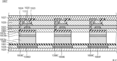
- the method for producing the LED sheet 1300 described below includes a step of forming a plurality of second buffer layer precursors in a plate shape (dot shape) on a non-oriented substrate (14th step), and a second buffer layer precursor.
- Annealing a member formed on the non-oriented substrate to form a plurality of second buffer layers in a plate shape on the non-oriented substrate (15th step), and on the plurality of second buffer layers A step of epitaxially growing the light emitting layer to form a plurality of pillars (step 16), a step of removing a part of the light emitting layer of each pillar (step 17), and a plurality of partially removed pillars Forming a first wiring (18th step), forming an insulating layer filling the space between the plurality of pillars (19th step), and a plurality of second buffers of the light emitting layer of the plurality of pillars Forming a second wiring on a surface opposite to the surface facing the layer Having a 20th step) and. Note that the order of the steps can be changed within a possible range.
- a method for manufacturing the LED sheet 1300 will be described with reference to the process diagrams of FIGS.
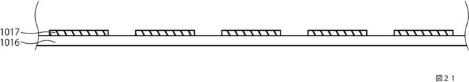
- FIG. 21 shows a step (fourteenth step) in which a plurality of alloys as second buffer layer precursors 1017 are formed in a plate shape on a non-oriented substrate 1016.
- the non-oriented substrate 1016 may be anything as long as there is no crystal orientation that is uniquely determined over the entire surface of the substrate, such as glass, metal, polycrystal, plastic (resin), ceramics, and amorphous.
- the non-oriented substrate 1016 is not particularly limited as long as it holds the hexagonal compound layer 2 necessary for epitaxial growth.
- the non-oriented substrate 1016 need not use an expensive single crystal base material.
- the light emitting element does not include the non-oriented substrate 1016 but is included in the LED sheet 1300.
- the LED sheet 1300 is not flexible. It is possible to make it flexible by bonding and fixing to a flexible substrate after device fabrication, laser lift-off from the non-oriented substrate 1016 side, or the like.
- the second buffer layer precursor 1017 is a metal alloy formed in a plate shape.
- the first buffer layer precursor 1007 that is a metal alloy is formed in a plate shape by forming and patterning a metal alloy film by sputtering or vapor deposition.
- the second buffer layer precursor 1017 includes Mg, Ca, Sc, Ti, Fe, Co, Ni, Zn, Sr, Y, Zr, Tc, Ru, Cd, In, Sn, Sb, Ba, Hf, Re, Os. And an alloy containing one or more metals selected from the group consisting of Pb. From the viewpoint of epitaxial growth, it is preferable that all the plate-like second buffer layer precursors 1017 and the second buffer layer precursors 1017 have the same composition.
- the metal of the second buffer layer precursor 1017 is selected according to the light emitting layer 1013 to be epitaxially grown.
- Annealing is performed in an inert gas atmosphere. By this heat treatment, the crystal of the alloy of the second buffer layer precursor 1017 on the non-oriented substrate 1016 is changed to form the second buffer layer 1012. It is important to perform c-axis orientation and single crystallization by heat treatment under predetermined annealing conditions. Before annealing, the crystal system is not hexagonal, but is often amorphous and non-oriented.
- the crystal system is hexagonal, c-axis oriented, alloyed, and single crystal (single grained) after annealing. It is.
- the annealing method is by laser heating or an electric furnace. Annealing conditions (atmosphere, temperature, time, etc.) are selected according to the light emitting layer 1013 to be epitaxially grown. It is preferable that all the plate-like second buffer layers 1012 have the same composition.
- FIG. 23 shows a step (sixteenth step) in which a light emitting layer 1013 is epitaxially grown on a plurality of second buffer layers 1012 to form a plurality of columnar objects.
- the columnar body includes one second buffer layer 1012 and a light emitting layer 1013 formed on the second buffer layer 1012. Since the lattice constant of the buffer layer 13 is matched with the lattice constant of the layer to be epitaxially grown, the light emitting layer 1013 is epitaxially grown on the second buffer layer 1012. Since the growth hardly occurs on the non-oriented substrate 1016, the light emitting layer 1013 is selectively grown on the second buffer layer 1012.
- the light emitting layer 1013 includes a plurality of layers, epitaxial growth is performed a plurality of times, and the light emitting layer 1013 is epitaxially grown on the plurality of second buffer layers 1012 to form a plurality of columnar objects.
- FIG. 24 shows a step of removing a part of each columnar light-emitting layer 1013 (a 17th step).
- a part of the light emitting layer 1013 is removed by, for example, ashing to form a region (extended surface) where the light emitting layer 1013 can contact the first wiring 1011. Ashing is performed to form a region where electrode contact can be made.
- FIG. 25 shows a step of forming the first wiring 1011 on the plurality of partially removed columnar objects (eighteenth step).
- the first wiring 1011 is formed in a region that can contact the first wiring 1011 formed by ashing or the like.
- FIG. 26 shows a step (19th step) of forming an insulating layer 1015 filling between a plurality of columnar objects.
- An insulating layer 1015 is formed so as to fill a space between columnar members of a member in which a plurality of columnar materials are formed on the non-oriented substrate 1016.
- the insulating layer 1015 can be formed by spraying, spin coating, or the like.
- the insulating layer 1015 may expose a part of the columnar object on the side opposite to the non-oriented substrate 1016 side, or the columnar object may be completely covered. If necessary, since the light emitting layer 1013 is in direct contact with the second wiring 1014, a part of the insulating layer 1005 can be removed to expose at least part of the surface of the light emitting layer 1003.
- step 20 a step of forming the second wiring on the surface opposite to the surface facing the plurality of second buffer layers 1012 of the plurality of columnar light emitting layers 1013 (step 20) is performed, and the LED sheet 1300 shown in FIG. Can be produced.
- the LED sheet 1300 modifications from the first embodiment to the seventh embodiment can be employed. Further, the LED sheet 1300 can be used for a display device, a lighting device, and the like as shown in the eighth embodiment.
- the tenth embodiment relates to an LED sheet.
- the LED sheet of the tenth embodiment has a specific configuration of the drive element 1010.
- FIG. 27 shows an LED sheet 1007 according to the tenth embodiment.
- An LED sheet 1007 shown in FIG. 27 has a configuration in which a TFT is provided on the anode side of the LED sheet described above.
- the LED sheet 1007 shown in FIG. 27 includes a first wiring 1001, a light emitting layer 1003 composed of an n-type semiconductor layer 1003a, an active layer 1003b, and a p-type semiconductor layer 1003c, a second wiring 1004, an insulating layer 1005, and a white phosphor 1008C.
- the second wiring 1004 is provided for each light emitting layer 1003. For example, if the light emitting layer 1003 has a hexagonal shape, the second wiring 1004 can similarly have a hexagonal shape.
- the LED sheet 1007 has a configuration in which, for example, the light emitting layer 1003 emits blue light, and the light passing through the white phosphor 1008C passes through the color filters 1008D to F.
- the light emitting layer 1003 emits blue light
- the light passing through the white phosphor 1008C passes through the color filters 1008D to F.
- one pixel is composed of three light emitting layers 1003.
- an insulating film 1028 may be disposed between the color filters 1008D to 1008F, and a protective film 1029 may be provided on the outermost surface.
- control semiconductor layer 1020 polysilicon, amorphous silicon, an amorphous oxide compound semiconductor, or the like is used.
- oxide compound semiconductor include IGZO.
- the control semiconductor layer 1020 is connected to the gate electrode 1022 through the gate insulating film 1021, connected to the drain electrode 1023, and connected to the source electrode 1024.
- a second wiring 1004 that is an anode electrode of the diode (light emitting layer 1003) is connected to the source electrode 1024, and a first wiring 1001 that is a cathode electrode of the diode (light emitting layer 1003) is a common electrode, and a plurality of diodes are connected. It is in contact with the n-type semiconductor layer. Driving of each light emitting layer 1003 of the LED sheet 1007 is controlled by the TFT.
- a manufacturing method of the LED sheet 1107 of the tenth embodiment will be described. 28
- a first buffer layer 1002 is provided over a non-oriented substrate 1006, and an insulating film 1009 is provided between the first buffer layers 1002.
- the insulating film 1009 is a film for peeling the first buffer layer 1002 together with the non-oriented substrate 1006.
- the first buffer layer 1002 can be removed even if the insulating film 1009 is omitted.
- the light emitting layer 1002 is grown on the member of FIG. 28 by the method described in the above embodiment.
- a p-type semiconductor layer 1003a is epitaxially grown on the first buffer layer 1002, and then an active layer 1003b and a p-type semiconductor layer 1003c are grown.
- the second wiring 1004 is formed.
- the second wiring 1004 preferably covers the p-type semiconductor layer 1003c to the extent that it does not contact the active layer 1003b.
- the second wiring 1004 may use a metal film that functions as a reflector.
- a known semiconductor manufacturing process is adopted for the member of FIG. 29 to form a TFT. Since the driving element 1020 including the control semiconductor layer 1020 and the light emitting layer 1003 are stacked in the direction from the first wiring 1001 to the second wiring 1004, the aperture ratio is reduced by positioning the TFT over the semiconductor light emitting layer. prevent.
- Another advantage of the embodiment is that the TFTs are not arranged in the direction in which the light emitting layers 1002 are arranged, so that the layout of the light emitting layer 1002 is not limited by the TFTs.
- a process of forming the first wiring 1001 is performed. Then, an LED sheet is formed, and a phosphor, a color filter, and the like are formed to obtain the LED sheet of FIG.
- FIG. 32 shows an equivalent circuit diagram of a part of the tenth embodiment.
- D is the light emitting element of the embodiment
- the first transistor T1 is the driving element 1010
- the second transistor T2 is a switching TFT
- the third transistor T3 is a light emission time control TFT.
- the gate electrode 1022 is electrically connected to the source electrode of the second transistor T2.
- the control line cn1 is connected to the gate electrode
- the signal line sg1 is connected to the drain electrode.
- the source electrode 1024 is electrically connected to the p-type semiconductor layer 1003c (second wiring 1004).
- the drain electrode 1023 is electrically connected to the third transistor T3.
- the control line cn2 is connected to the gate electrode of the third transistor T3.
- the third transistor T3 has a source electrode connected to the first transistor T1 and a drain electrode connected to the high potential terminal PVDD.
- the n-type semiconductor layer 1003a (first wiring 1001) side is a low potential end PVSS.
- the light emission timing and the duty ratio can be controlled by the signals (timing chart) from the control lines cn1 and cn2, and light can be emitted efficiently.
- the structure shown in the equivalent circuit of FIG. 32 is an example of a driver circuit for a light-emitting element.
- the eleventh embodiment relates to an LED sheet.
- the LED sheet of the eleventh embodiment enables the LED sheet to display in full color by emitting light of different colors from the light emitting layer 1003 itself.
- FIG. 33 is a conceptual diagram of an LED sheet for one pixel.
- the hexagonal shape represents the light emitting layer 1003, and G, B, and R written on each represent the color of the emitted light (G: green, B: blue, R: red).
- G green, B: blue, R: red
- GaN material blue efficiency is high, and green and red have low luminous efficiency. Therefore, by increasing the number of green and red light emitting layers 1003 to two or more for one blue light emitting layer 1003, the amount of emitted light of each color is balanced. By performing different wiring for each color, it is possible to control for each color.
- the twelfth embodiment relates to an LED sheet.
- the LED sheet of the eleventh embodiment is a form in which a light emitting layer group 1003G composed of a plurality of light emitting layers 1003 emits light as one color of one pixel.
- FIG. 34 is a conceptual diagram of an LED sheet for one pixel.
- the light emitting layer group 1003G is sandwiched between electrodes that electrically connect a plurality of light emitting layers 1002 such as a solid film, and the light emitting layer group 1003G is controlled by electricity from a common solid film electrode.
- the size of the light emitting layer 1003 is not uniform, but the size of the light emitting layer 1003 may be uniform.
- the shape of the light emitting layer 1003 is uniform or not uniform as shown in FIG. 34, it is possible to suppress variations in luminance by controlling the plurality of light emitting layers 1003 as one color of one pixel.
- the redundancy is improved and the yield is increased.
- a hexagonal shape is adopted, stress is easily dispersed when bent, which is preferable from the viewpoint of flexibility.
- a high refractive index material can be used for the insulating layer 1005 so that total reflection at the interface between the light emitting layer 1003 and the insulating layer 1005 is difficult.
- the thirteenth embodiment relates to an LED sheet.
- the LED sheet of the thirteenth embodiment has a configuration in which a plurality of LED sheets having different emission colors are stacked. The color of light emitted from each LED sheet can be changed by changing the composition of the light emitting layer 1003 or the like.
- FIG. 35 shows an LED sheet 1108 of the thirteenth embodiment. By overlapping the LED sheet 1107R that emits red light, the LED sheet 1107G that emits green light, and the LED sheet 1107B that emits blue light so that the light emitting layer 1003 does not overlap, full color display is possible.
- the LED sheet on which the amorphous oxide TFT is formed is excellent in flexibility and is a very thin film.
- Example 1-1 As the substrate, a 10 cm square glass substrate (made of quartz) having a thickness of 1 mm was prepared. A resist was applied on the substrate, and vertical holes with a diameter of 5 ⁇ m were formed by photolithography. A Mo film was formed to 100 nm by a vapor deposition method, and Mo dots were formed by lift-off. Annealing was performed at 1000 ° C. in an atmosphere of sulfur and selenium 4: 1 to form Mo (S 0.8 Se 0.2 ) 2 in a single crystal state. When this was taken out and the a-axis length of the molybdenum selenide sulfide compound was determined by X-ray diffraction, it was 3.189 mm.
- a light emitting element portion was fabricated in the order of n-type GaN, GaN quantum well, and p-type GaN.
- Cytop manufactured by Asahi Kasei
- Cytop was applied as an insulating layer, and only the light emitting layer portion was exposed by photolithography and oxygen plasma.
- a stripe-shaped transparent electrode was formed so as to connect adjacent light emitting element portions in the linear direction, and then a glass plate coated with resin was covered and fixed, and peeled off from the quartz substrate.
- a striped transparent electrode was formed so as to connect adjacent light emitting element portions so as to intersect the striped transparent electrode in a straight line.
- RBG pixels were formed using a green phosphor and a red phosphor to form a passive matrix display. Thereafter, the glass substrate was peeled off to obtain a flexible display.
- Example 1-2 As the substrate, a 10 cm square glass substrate (made of quartz) having a thickness of 1 mm was prepared. A resist was applied on the substrate, and vertical holes with a diameter of 5 ⁇ m were formed by photolithography. A Mo film was formed to 100 nm by a vapor deposition method, and Mo dots were formed by lift-off. Annealing was performed at 1000 ° C. in an atmosphere of sulfur and selenium 4: 1 to form Mo (S 0.8 Se 0.2 ) 2 in a single crystal state. When this was taken out and the a-axis length of the molybdenum selenide sulfide compound was determined by X-ray diffraction, it was 3.189 mm.
- a light emitting element portion was fabricated in the order of n-type GaN, GaN quantum well, and p-type GaN.
- Cytop manufactured by Asahi Kasei
- a transparent electrode was formed so as to connect the entire surface of the light emitting element portion, and then a glass plate coated with a resin was covered and fixed, and then peeled off from the quartz substrate.
- One TFT was formed for each pixel, and red and green quantum dots were applied to form RBG pixels, thereby forming an active matrix display. Thereafter, the glass substrate was peeled off to obtain a flexible display.
- the quantum dots are changed slightly from Example 1-1. The effect is the same.
- Example 1-3 As the substrate, a 10 cm square glass substrate (made of quartz) having a thickness of 1 mm was prepared. A resist was applied on the substrate, and vertical holes with a diameter of 5 ⁇ m were formed by photolithography. A Mo film was formed to 100 nm by a vapor deposition method, and Mo dots were formed by lift-off. Annealing was performed at 1000 ° C. in an atmosphere of sulfur and selenium 4: 1 to form Mo (S 0.8 Se 0.2 ) 2 in a single crystal state. When this was taken out and the a-axis length of the molybdenum selenide sulfide compound was determined by X-ray diffraction, it was 3.189 mm.
- a light emitting element portion was fabricated in the order of n-type GaN, GaN quantum well, and p-type GaN.
- Cytop manufactured by Asahi Kasei
- One TFT was formed for one light emitting element, and a glass plate coated with resin was covered and fixed, and peeled off from the quartz substrate. After peeling, the entire surface of the light emitting element was covered with a transparent electrode, RBG pixels were formed using a green phosphor and a red phosphor, and an active matrix display was formed. Thereafter, the glass substrate was peeled off to obtain a flexible display.
- a 10 cm square glass substrate made of quartz having a thickness of 1 mm was prepared.
- a resist was applied on the substrate, and vertical holes with a diameter of 5 ⁇ m were formed by photolithography.
- a Mo film was formed to 100 nm by a vapor deposition method, and Mo dots were formed by lift-off.
- Annealing was performed at 1000 ° C. in an atmosphere of sulfur and selenium 4: 1 to form MoSe 2 in a single crystal state. When this was taken out and the a-axis length of the molybdenum selenide compound was determined by X-ray diffraction, it was 3.288 mm.
- a light emitting element portion was fabricated in the order of n-type GaN, GaN quantum well, and p-type GaN.
- Cytop manufactured by Asahi Kasei
- Cytop was applied as an insulating layer, and only the light emitting layer portion was exposed by photolithography and oxygen plasma.
- a stripe-shaped transparent electrode was formed so as to connect adjacent light emitting element portions in the linear direction, and then a glass plate coated with resin was covered and fixed, and peeled off from the quartz substrate.
- a striped transparent electrode was formed so as to connect adjacent light emitting element portions so as to intersect the striped transparent electrode in a straight line.
- RBG pixels were formed using a green phosphor and a red phosphor to form a passive matrix display. Thereafter, the glass substrate was peeled off to obtain a flexible display. However, the device did not emit light. This is probably because the difference in lattice constant between GaN and molybdenum selenide compound is large, and a large amount of crystal defects exist in the light emitting element portion.
- Example 2-1 As the substrate, a 10 cm square glass substrate (made of quartz) having a thickness of 1 mm was prepared. A resist was applied on the substrate, and vertical holes having a diameter of 10 ⁇ m were formed by photolithography. An Hf—Ti film having a thickness of 100 nm was formed by vapor deposition, and Hf—Ti dots were formed by lift-off. Annealing was performed at 1000 ° C. to form Hf—Ti dots in a single crystal state. When this was taken out and the a-axis length of the metal alloy was determined by X-ray diffraction, it was 3.189 mm.
- a light emitting element portion was fabricated in the order of n-type GaN, GaN quantum well, and p-type GaN. Ashing was partially cut to form a lower electrode in a stripe shape. Cytop (manufactured by Asahi Kasei) was applied as an insulating layer, dried, and only the light emitting layer portion was exposed by photolithography and oxygen plasma. After forming the stripe-shaped upper transparent electrode so as to cross the straight line with the stripe-shaped lower electrode and to connect the adjacent light emitting element portions in the linear direction, the RBG pixel is formed using the green phosphor and the red phosphor. The passive matrix type display was formed.
- Example 2-2 As the substrate, a 10 cm square glass substrate (made of quartz) having a thickness of 1 mm was prepared. A resist was applied on the substrate, and vertical holes having a diameter of 10 ⁇ m were formed by photolithography. An Hf—Ti film having a thickness of 100 nm was formed by vapor deposition, and Hf—Ti dots were formed by lift-off. Annealing was performed at 1000 ° C. to form Hf—Ti dots in a single crystal state. When this was taken out and the a-axis length of the metal alloy was determined by X-ray diffraction, it was 3.189 mm.
- a light emitting element portion was fabricated in the order of n-type GaN, GaN quantum well, and p-type GaN. Ashing was partially cut to form a lower electrode in a mesh shape. Cytop (manufactured by Asahi Kasei) was applied as an insulating layer, dried, and only the light emitting layer portion was exposed by photolithography and oxygen plasma.
- TFT was formed for one light emitting element, RBG pixels were formed using a green phosphor and a red phosphor, and an active matrix display was formed.
- Example 2-3 As the substrate, a 10 cm square glass substrate (made of quartz) having a thickness of 1 mm was prepared. A resist was applied on the substrate, and vertical holes having a diameter of 10 ⁇ m were formed by photolithography. A Zr—Ti film having a thickness of 100 nm was formed by vapor deposition, and Zr—Ti dots were formed by lift-off. Annealing was performed at 1000 ° C. to form Zr—Ti dots in a single crystal state. The a-axis length of the alloy was determined by X-ray diffraction and found to be 3.112 mm.
- a light emitting element portion was fabricated in the order of an underlayer composed of AlN and GaN, a quantum well, and a p-type layer. Ashing was partially cut to form a lower electrode in a mesh shape. Cytop (manufactured by Asahi Kasei) was applied as an insulating layer, and only the light emitting layer portion was exposed by photolithography and oxygen plasma. After forming a mesh-like rhodium electrode so as to connect the light emitting element portions, a glass plate coated with resin is covered and fixed, whereby a deep ultraviolet light emitting element is obtained.
- a 10 cm square glass substrate made of quartz
- a resist was applied on the substrate, and vertical holes having a diameter of 10 ⁇ m were formed by photolithography.
- An Mg film having a thickness of 100 nm was formed by vapor deposition, and Hf—Ti dots were formed by lift-off. Annealing was performed at 1000 ° C. to form Mg dots in a single crystal state. When this was taken out and the a-axis length of the metal alloy was determined by X-ray diffraction, it was 3.210 mm.
- a light emitting element portion was fabricated in the order of n-type GaN, GaN quantum well, and p-type GaN. Ashing was partially cut to form a lower electrode in a stripe shape. Cytop (manufactured by Asahi Kasei) was applied as an insulating layer, dried, and only the light emitting layer portion was exposed by photolithography and oxygen plasma. After forming the stripe-shaped upper transparent electrode so as to cross the straight line with the stripe-shaped lower electrode and to connect the adjacent light emitting element portions in the linear direction, the RBG pixel is formed using the green phosphor and the red phosphor. The passive matrix type display was formed. However, the device did not emit light. This is probably because the lattice constant difference between GaN and ceMg is large, and a large amount of crystal defects exist in the light emitting element portion.
- Technical proposal 1 A plurality of light emitting elements in which a first wiring, a first buffer layer (layered compound layer), a light emitting layer including a diode, and a second wiring are sequentially stacked; And at least an insulating layer disposed between the plurality of light emitting elements, The first wiring is in direct contact with the first buffer layer, The second wiring is in direct contact with the light emitting layer, The light-emitting diode sheet, wherein a surface of the first buffer layer directly in contact with the first wiring is opposite to a surface of the first buffer layer facing the second wiring.
- Technical plan 2 The light emitting diode sheet according to the technical solution 1, wherein a surface of the insulating layer facing the light emitting element is in direct contact with at least a part of a surface of the light emitting element facing the insulating layer.
- Technical plan 3 The plurality of light emitting elements are electrically connected via the first wiring, The light emitting diode sheet according to Technical Solution 1 or 2, wherein the plurality of light emitting elements are electrically connected via the second wiring.
- the light emitting layer has a heteroepitaxial relationship in which a plurality of layers are stacked, The first buffer layer and the light emitting layer are in direct contact with each other, A technique in which a difference between an in-plane lattice constant of the first buffer layer and an in-plane lattice constant of a layer that is closest to the first buffer layer among light emitting layers in which the plurality of layers are stacked is within a range of ⁇ 1%. 4.
- Technical plan 5 The light emitting diode sheet according to any one of the technical solutions 1 to 4, wherein the first buffer layer layer includes a metal chalcogenide.
- the first buffer layer includes a layered compound represented by MSe ⁇ S ⁇ Te ⁇ O ⁇ ,
- the M is Ti, Zr, Hf, V, Nb, Ta, Cr, Mo, W, Zn, Cd, Ga, In, Ge, Sn, Pt, Au, Cu, Ag, Mn, Fe, Co, Ni, One or more selected from the group consisting of Pb and Bi;
- the ⁇ , ⁇ and ⁇ are 0.0 ⁇ ⁇ ⁇ 2.0, 0.0 ⁇ ⁇ ⁇ 2.0, 0.0 ⁇ ⁇ ⁇ 2.0, 0.0 ⁇ ⁇ ⁇ 2.0 and 1.
- the first buffer layer includes a layered compound represented by MSe ⁇ S ⁇ Te ⁇ O ⁇ , M includes at least one selected from the group consisting of Mo, W and Cr, The ⁇ , ⁇ and ⁇ are 0.0 ⁇ ⁇ ⁇ 2.0, 0.0 ⁇ ⁇ ⁇ 2.0, 0.0 ⁇ ⁇ ⁇ 2.0, 0.0 ⁇ ⁇ ⁇ 2.0 and 1. 7.
- the diameter of the first buffer layer is in the range of 0.1 ⁇ m to 200 ⁇ m; 8.
- Technical plan 9 The shortest distance between the centers of the first buffer layers of the plurality of light emitting elements is 0.5 ⁇ m or more and 500 ⁇ m or less, The light emitting diode sheet according to any one of the technical solutions 1 to 8, wherein a shortest distance between centers of the light emitting layers of the plurality of light emitting elements is 0.5 ⁇ m or more and 500 ⁇ m or less.
- Technical plan 10 A plurality of light emitting elements in which a first wiring, a light emitting layer including a diode, and a second wiring are sequentially stacked; And at least an insulating layer disposed between the plurality of light emitting elements, The light emitting layer is in direct contact with the first wiring, The light emitting diode sheet
- Technical plan 11 The light emitting diode sheet according to the technical plan 10, wherein a surface of the insulating layer facing the light emitting element is in direct contact with at least a part of a surface of the light emitting element facing the insulating layer.
- Technical plan 12 The plurality of light emitting elements are electrically connected via the first wiring, The light emitting diode sheet according to the technical solution 10 or 11, wherein the plurality of light emitting elements are electrically connected via the second wiring.
- Technical plan 13 13 The light emitting diode sheet according to any one of the technical solutions 9 to 12, wherein the diameter of the light emitting layer is in a range of 0.1 ⁇ m to 200 ⁇ m.
- Technical proposal 14 The light emitting diode sheet according to any one of the technical solutions 9 to 13, wherein a shortest distance between centers of the light emitting layers of the plurality of light emitting elements is 0.5 ⁇ m or more and 500 ⁇ m or less.
- Technical plan 15 A display device using the light-emitting diode sheet according to any one of the technical solutions 1 to 14.
- Technical plan 16 Forming a plurality of first buffer layer precursors in a plate shape on a non-oriented substrate; Heating the member in which the first buffer layer precursor is formed on a non-oriented substrate to form a plurality of first buffer layers containing a layered compound on the non-oriented substrate in a plate shape; Forming a plurality of pillars by epitaxially growing a light emitting layer on the plurality of first buffer layers; Forming an insulating layer filling the space between the plurality of pillars; Forming a second wiring on a surface of the light emitting layer of the plurality of columnar objects opposite to a surface facing the plurality of first buffer layers; Peeling the non-oriented substrate and forming a first wiring on a surface of the plurality of columnar objects opposite to the surface facing the light emitting layer of the plurality of layered compounds; A method for producing a light-emitting diode
- the first buffer layer includes a layered compound represented by MSe ⁇ S ⁇ Te ⁇ O ⁇ , M includes at least one selected from the group consisting of Mo, W and Cr,
- the ⁇ , ⁇ and ⁇ are 0.0 ⁇ ⁇ ⁇ 2.0, 0.0 ⁇ ⁇ ⁇ 2.0, 0.0 ⁇ ⁇ ⁇ 2.0, 0.0 ⁇ ⁇ ⁇ 2.0 and 1.
- Technical plan 20 The diameter of the plurality of columnar objects is in the range of 0.1 ⁇ m to 200 ⁇ m, The method for manufacturing a light-emitting diode sheet according to any one of the technical solutions 15 to 18, wherein the shortest distance between the centers of the plurality of columnar objects is 0.5 ⁇ m or more and 500 ⁇ m or less.
- the fourteenth embodiment relates to a light emitting diode sheet (hereinafter referred to as an LED sheet).
- the LED sheet includes a first wiring, a layered compound layer, a light emitting layer including a diode, a plurality of light emitting elements in which second wirings are sequentially stacked, and an insulating layer disposed between the plurality of light emitting elements.
- the emission wavelength can be changed.
- the LED sheet can also emit ultraviolet light. By emitting visible light, the LED sheet can be used as illumination.
- the LED sheet can be used as a sheet for emitting ultraviolet light by emitting ultraviolet light. Ultraviolet rays on the order of 200 nm to 300 nm are strong in energy and are suitable for sterilization performed by decomposing DNA or the like.
- FIG. 36 shows a perspective view of the LED sheet 2100.
- FIG. 37 shows a cross-sectional view of the LED sheet 2100.
- the LED sheet 2100 includes a plurality of light emitting elements in which a first wiring 2001, a first buffer layer 2002, a light emitting layer 2003 including a diode, and a second wiring 2004 are sequentially stacked.
- An insulating layer 2005 is disposed.
- the first wiring 2001 extends in the first direction
- the second wiring 2004 extends in the second direction.
- the light emitting elements are uniformly arranged in the first direction and the second direction with the same size, but the size and arrangement of the light emitting elements are limited to the form illustrated in FIGS. It is not a thing.
- the LED sheet 2100 has a first surface and a second surface opposite to the first surface, a plurality of light emitting elements having a light emitting layer 2003 including a diode, and an insulating layer 2005 disposed between the plurality of light emitting elements.
- the first wiring 2001 provided on the first surface side of the light emitting layer 1003 of the plurality of light emitting elements, and the second wiring 2004 provided on the second surface side of the light emitting layer 2003 of the plurality of light emitting elements.
- the LED sheet 2100 has a configuration in which a light emitting element is disposed in an insulating layer 2005.
- a flexible polymer or the like for the insulating layer 2005, the LED sheet 2100 can be made flexible. Flexible means that the LED sheet 2100 is not broken, chipped, or damaged by repeated winding and releasing 10 times slowly on a cylindrical rod having a diameter of 200 mm under an atmospheric pressure environment of 25 ° C. Say.
- the LED sheet 2100 does not include an epitaxial growth substrate for growing the light emitting layer 2003 and is not used in production, the LED sheet 2100 can be produced at low cost.
- the size of the LED sheet 2100 varies from tens of mm 2 to more than 1 m 2 . Since it can be manufactured at a lower cost than the conventional one, a design that can irradiate the target with an effective arrangement becomes possible.
- the LED sheet 2100 that emits ultraviolet light is wound around a transparent pipe, the object passing through the pipe can be sterilized.
- the LED sheet 2100 may be fixed to a glass or resin substrate (not shown).
- the first wiring 2001 is a conductor that is in direct contact with the first buffer layer 2002.
- the first wiring 2001 is an electrode of each light emitting element.
- the first wiring 2001 serves as one of the anode and the cathode of the light emitting layer 2003.
- the first wiring 2001 is in direct contact with the first buffer layer 2002.
- the surface of the first buffer layer 2002 that is in contact with the first wiring 2001 is the opposite side of the surface of the first buffer layer 2002 that faces the second wiring 2004. It is preferable that the plurality of light emitting elements included in the LED sheet 2100 are electrically connected via the first wiring 2001.
- the first wiring 2001 is a single anode electrode of the LED sheet 2100
- the second wiring 2004 is a single cathode electrode of the LED sheet 2100
- the first wiring 2001 is a single cathode electrode of the LED sheet 2100
- the second wiring 2004 is a single anode electrode of the LED sheet 2100. That is, the LED sheet 2100 is an element that is in two states, that is, all the light emitting elements emit light or all the light emitting elements do not emit light except for defects and failures.
- the first wiring 2001 includes either a metal film or a transparent conductive film.
- the first wiring 2001 can be a transparent electrode.
- the first wiring 2001 may be a laminated film.
- the first wiring 2001 is a line-shaped, mesh-shaped, or film-shaped conductor, and a plurality of light-emitting elements are electrically connected by a line-shaped, mesh-shaped, or film-shaped conductor.
- the line-shaped conductor is a single line or bundled.
- the first wiring 2001 is preferably a metal electrode that also serves as a reflector.
- the first wiring 2001 is preferably a stripe-shaped or mesh-shaped metal film or a transparent conductive film.
- the first wiring 2001 It is preferable to use a stripe-shaped or mesh-shaped metal film. In addition, it is good also as a double-sided light emission type LED sheet which makes the both sides of the 1st wiring 2001 and the 2nd wiring 2004 light emission.
- the first wiring 2001 may be able to electrically connect all the light emitting elements arranged as shown in FIG. 36 and FIG. Since it is not necessary to individually control the light emission of the plurality of light emitting elements, the first wiring is preferably a film-like conductor. Further, it is preferable that the first wiring 2001 electrically and directly connects all the light emitting elements.
- the first buffer layer 2002 includes a layered compound.
- the first buffer layer 2002 is preferably plate-shaped.
- the first buffer layer 2002 is preferably a layer made of a layered compound.
- the first buffer layer 2002 is disposed between the first wiring 2001 and the light emitting layer 2003.
- the surface of the first buffer layer 2002 facing the light emitting layer 2003 is opposite to the surface of the first buffer layer 2002 facing the first wiring 2001.
- the first buffer layer 2002 is a single crystal containing a plurality of two-dimensional sheet-like layered compounds, and the crystal orientation of the surface facing the light emitting layer 2003 of the first buffer layer 2002 (crystal orientation of the layered compound) is uniform. is there.
- the crystallinity of the first buffer layer 2002 is determined by 4-axis X-ray diffraction measurement or observation with a transmission electron microscope.
- a two-dimensional layered material such as graphene, a hexagonal metal such as hafnium or an alloy, or a ceramic may be used.
- the layered compound is a two-dimensional sheet extending in the surface direction of the first buffer layer 2002.
- a metal chalcogenide is preferable.
- graphene is also a layered compound, graphene cannot change the lattice constant according to the light emitting layer 2003.
- the lattice constant of the layered compound can be controlled by selecting the metal and the chalcogen element and the ratio thereof.
- a metal chalcogenide represented by MSe ⁇ S ⁇ Te ⁇ O ⁇ is preferable.
- M which is a metal contained in the metal chalcogenide is Ti, Zr, Hf, V, Nb, Ta, Cr, Mo, W, Zn, Cd, Ga, In, Ge, Sn, Pt, Au, Cu, Ag, Mn , Fe, Co, Ni, Pb, and Bi.
- ⁇ , ⁇ and ⁇ are 0.0 ⁇ ⁇ ⁇ 2.0, 0.0 ⁇ ⁇ ⁇ 2.0, 0.0 ⁇ ⁇ ⁇ 2.0, 0.0 ⁇ ⁇ ⁇ 2.0 and 1.0. It is preferable that ⁇ ⁇ + ⁇ + ⁇ + ⁇ ⁇ 2.0 is satisfied.
- ⁇ , ⁇ and ⁇ are 0.0 ⁇ ⁇ ⁇ 2.0, 0.0 ⁇ ⁇ ⁇ 2.0, 0.0 ⁇ ⁇ ⁇ 2.0, 0.0 ⁇ ⁇ ⁇ 2.0, 0 0.0 ⁇ + ⁇ + ⁇ and 1.0 ⁇ ⁇ + ⁇ + ⁇ + ⁇ ⁇ 2.0 are preferably satisfied.
- M which is a metal contained in the metal chalcogenide, preferably contains at least one selected from the group consisting of Mo, W, and Cr. The selection and ratio of metal chalcogenide elements are changed according to the light emitting layer 2003 to be epitaxially grown.
- the diameter (D1) of the first buffer layer 2002 is in the range of 0.1 ⁇ m to 200 ⁇ m. Within this range, the light source is suitable for a light emitting device.
- the diameter of the first buffer layer 2002 the inscribed circle diameter and the circumscribed circle diameter of each first buffer layer 2002 are obtained in a cross section perpendicular to the stacking direction of the light emitting elements.
- the average value of the determined inscribed circle diameter and circumscribed circle diameter is defined as the diameter of each layered compound layer.
- the diameter of the columnar body in which the first buffer layer 2002 and the light emitting layer 2003 are stacked depends on the diameter of the first buffer layer 2002.
- the diameter of the first buffer layer 2002 (columnar material) is preferably 1 ⁇ m or more and 200 ⁇ m or less, or 5 ⁇ m or more and 100 ⁇ m or less.
- the cross-sectional area and the diameter of the first buffer layer 2002 are preferably changed according to required luminance or the like.
- the plate shape (cross-sectional shape) of the first buffer layer 2002 is often a polygonal column shape such as a disc shape, a triangular column shape, or a hexagonal column shape, but may be any plate shape.
- the shapes of the adjacent first buffer layers 2002 may be different.
- the shortest distance (D2) between the centers of the first buffer layers 2002 (columnar objects) of the plurality of light emitting elements is 0.5 ⁇ m or more and 300 ⁇ m or less.
- a plurality of light emitting elements are included in the LED sheet 10. The plurality of light emitting elements are separated from each other, and there is a gap between the plurality of light emitting elements.
- the shortest distance between the centers of the first buffer layers 2002 of the plurality of light emitting elements is obtained as follows. First, the center point of the first buffer layer 2002 of one light emitting element and the center point of the first buffer layer 2002 of a plurality of light emitting elements around it are obtained.
- the shortest distance among the distances between the center point of the first buffer layer 2002 of one light emitting element and the center point of the first buffer layer 2002 of the plurality of light emitting elements on the outer periphery of the light emitting element is determined by the plurality of light emitting elements.
- the shortest distance between the centers of the first buffer layers 2002 is set.
- the center point of the first buffer layer 2002 of the light emitting element is the center of the circumscribed circle of the first buffer layer 2002.
- the shortest distance between the centers of the 1st buffer layer 2002 (columnar thing) of a several light emitting element it is more preferable that they are 20 micrometers or more and 300 micrometers or less.
- the number of pixels of the shortest distance product between the centers of the first buffer layers 2002 of the plurality of light emitting elements is changed.
- the thickness of the first buffer layer 2002 is not particularly limited.
- the thickness of the first buffer layer 2002 is, for example, not less than 10 nm and not more than 1000 nm.
- the variation in the thickness of the first buffer layer 2002 is preferably as small as possible.
- the first buffer layer 2002 and the light emitting layer 2003 are in a heteroepitaxial relationship.
- the stacking direction of the light emitting elements is parallel to the hexagonal c-axis of the metal chalcogenide.
- the metal chalcogenide perpendicular to the stacking direction of the light emitting elements is parallel to the hexagonal a and b axes.
- the orientation of the metal chalcogenide parallel to the substrate surface is random and is not particularly limited as viewed perpendicularly from the substrate surface.
- the metal chalcogenide can arbitrarily change the lattice constant by selecting the element, the lattice constant of the single crystal layer to be epitaxially grown and the lattice constant of the metal chalcogenide can be matched by changing the composition of the metal chalcogenide. That is, by changing the composition of the metal chalcogenide according to the single crystal layer to be epitaxially grown and the crystal orientation to be grown, for example, a substrate suitable for epitaxial growth such as GaN, InN, and AlN can be prepared. In these hexagonal nitrides, the plane orientation for growth is the 0001 direction.
- the difference between the in-plane lattice constant of the first buffer layer 2002 and the in-plane lattice constant of the layer that is closest to the first buffer layer 2002 among the light emitting layers 2003 in which a plurality of layers are stacked ([[the first buffer layer 2002 of In-plane lattice constant]-[in-plane lattice constant of the layer that is closest to the first buffer layer 2002 in the light emitting layer 2003] / [in-plane lattice constant of the first buffer layer 2002]) is within ⁇ 1%.
- the difference in lattice constant is large, epitaxial growth is difficult, and if the difference is large, epitaxial growth does not occur or crystal defects are likely to occur, so that the in-plane lattice constant of the first buffer layer 2002 and a plurality of layers are easily formed. More preferably, the difference in the in-plane lattice constant of the layer present on the first buffer layer 2002 side of the light emitting layer 2003 laminated with is within 0.5%.
- the lattice constant is obtained by 4-axis X-ray diffraction measurement, or is generally determined by the composition ratio of the metal chalcogenide constituting the first buffer layer 2002.
- the two-dimensional sheet-shaped metal chalcogenide that is in direct contact with the light emitting layer 2003 of the first buffer layer 2002 may be composed of a plurality of two-dimensional sheet-shaped metal chalcogenides.
- the surface of the first buffer layer 2002 that is in direct contact with the light emitting layer 2003 is arranged so that the crystal orientations of a plurality of two-dimensional sheet-shaped metal chalcogenides are aligned.
- a plurality of two-dimensional sheet-shaped metal chalcogenides may be overlapped, and there may be a step.
- the surface of the first buffer layer 2002 in direct contact with the light emitting layer 2003 is not a single two-dimensional sheet metal chalcogenide when peeling from the substrate used at the time of production, a plurality of two-dimensional sheet If the crystal orientation of the metal chalcogenide is uniform, the light emitting layer 2003 can be epitaxially grown on the first buffer layer 2002. Since epitaxial growth is possible even if it is not a perfect sheet, a member in which a plurality of first buffer layers 2002 are arranged on a substrate can be manufactured at low cost. And the production cost of an LED sheet can be suppressed by producing an LED sheet using the board
- the light emitting layer 2003 is a light emitting diode disposed between the first buffer layer 2002 and the second wiring 2004.
- the light emitting layer 2003 is in direct contact with the first buffer layer 2002 and in direct contact with the second wiring 2004.
- the surface in which the light emitting layer 2003 is in direct contact with the second wiring 2004 is opposite to the surface in direct contact with the first buffer layer 2002.
- the light emitting layer 2003 includes a first conductivity type semiconductor layer (compound semiconductor), an active layer, and a second conductivity type semiconductor layer (compound semiconductor).
- the light emitting layer 2003 includes a hexagonal nitride semiconductor layer.
- the light-emitting layer 2003 is preferably formed by stacking a plurality of hexagonal nitride semiconductor layers.
- the plurality of layers of the light emitting layer 2003 are preferably in a heteroepitaxial relationship.
- the nitride semiconductor layer is preferably a single crystal layer of GaN, InN, AlN, and two or more mixed compositions selected from the group consisting of GaN, InN, and AlN.
- the in-plane lattice constant of the nitride semiconductor layer has a width from 3.111 to 3.532.
- the metal chalcogenide can be adjusted to the in-plane lattice constant of the nitride semiconductor layer from 3.111 to 3.532.
- the metal chalcogenide composition ratio may be slightly changed in consideration of the difference in thermal expansion coefficient during film formation and the growth rate.
- the compound semiconductor (including the active layer) used for the light emitting layer 2003 includes GaN, InN, AlN, and two or more kinds of mixed compositions selected from the group consisting of GaN, InN, and AlN, as well as GaAs, etc.
- Examples include arsenic compound semiconductors and phosphorus compound semiconductors such as InGaAlP.
- the arsenic compound semiconductor and the phosphorus compound semiconductor can have the same in-plane lattice constant with the first buffer layer 2002 as in the case of the nitride semiconductor.
- An arsenic compound semiconductor or a phosphorus compound semiconductor can be preferably grown as the light emitting layer 2003 from the first buffer layer 2002. That is, the first conductivity type semiconductor layer, the active layer, and the second conductivity type semiconductor layer are semiconductor layers including at least one selected from the group consisting of nitride semiconductors, arsenic compound semiconductors, and phosphorus compound semiconductors. .
- the light emitting layer 2003 When the light emitting layer 2003 is a blue light emitting diode, the light emitting layer 2003 includes, for example, a first conductivity type GaN layer, a first conductivity type AlGaN layer, an InGaN layer, a second conductivity type AlGaN layer, and a second conductivity type.
- the GaN layers are stacked.
- the in-plane lattice constant of the first buffer layer 2002 is set to GaN.
- MoS 1.6 Se 0.4 for the metal chalcogenide, the lattice constants of the metal chalcogenide and GaN are matched.
- the light emitting layer 2003 When the light emitting layer 2003 is an ultraviolet light emitting diode, the light emitting layer 2003 has a structure in which, for example, a first conductive type AlN, an AlN light emitting layer and a second conductive type AlN are stacked.
- the in-plane lattice constant of the first buffer layer 2002 is set to AlN.
- Mo 0.6 Cr 0.4 S 2.0 for the metal chalcogenide the lattice constants of the metal chalcogenide and AlN match.
- the diameter (D3) of the light emitting layer 2003 is preferably in the range of 0.1 ⁇ m to 200 ⁇ m. Within this range, the light source is suitable for a light emitting device.
- the diameter of the light emitting layer 2003 the inscribed circle diameter and the circumscribed circle diameter of the light emitting layer 2003 are obtained in a cross section perpendicular to the stacking direction of the light emitting elements. The average value of the obtained inscribed circle diameter and circumscribed circle diameter is defined as the diameter of each light emitting layer 2003.
- the diameter of the columnar body in which the first buffer layer 2002 and the light emitting layer 2003 are stacked is affected by the diameter of the first buffer layer 2002.
- the diameter of the light emitting layer 2003 is preferably 1 ⁇ m or more and 200 ⁇ m or less, or 5 ⁇ m or more and 100 ⁇ m or less.
- the cross-sectional area and diameter of the light emitting layer 2003 are preferably changed according to required luminance or the like.
- the cross-sectional shape of the light emitting layer 2003 is often a polygonal prism shape such as a disc shape, a triangular prism shape, or a hexagonal prism shape, but is not particularly limited.
- the shapes of the adjacent light emitting layers 2003 may be different.
- the shortest distance (D4) between the centers of the light emitting layers 2003 of the plurality of light emitting elements is 0.5 ⁇ m or more and 300 ⁇ m or less.
- a plurality of light emitting elements are included in the LED sheet 10. The plurality of light emitting elements are separated from each other, and there is a gap between the plurality of light emitting elements.
- the shortest distance between the centers of the light emitting layers 2003 of the plurality of light emitting elements is obtained as follows. First, the center point of the light emitting layer 2003 of one light emitting element and the center point of the light emitting layer 2003 of a plurality of light emitting elements around it are obtained.
- the shortest distance between the center point of the light emitting layer 2003 of one light emitting element and the center point of the light emitting layer 2003 of the plurality of light emitting elements on the outer periphery of the light emitting element is the light emitting layer 2003 of the plurality of light emitting elements.
- the center point of the light emitting layer 2003 of the light emitting element is the center of the circumscribed circle of the light emitting layer 2003.
- the shortest distance between the centers of the light emitting layers 2003 of the plurality of light emitting elements is more preferably 5 ⁇ m or more and 300 ⁇ m or less, or 10 ⁇ m or more and 100 ⁇ m or less.
- the shortest distance between the centers of the light emitting layers 2003 of the plurality of light emitting elements is changed according to product specifications and the like.
- the second wiring 2004 is a conductor that is in direct contact with the surface of the light emitting layer 2003 opposite to the surface facing the first buffer layer 2002.
- the second wiring 2 is an electrode of each light emitting element. It is preferable that the plurality of light emitting elements included in the LED sheet 2100 are electrically connected via the second wiring 2004.
- the second wiring 2004 includes either a metal film or a transparent conductive film.
- the second wiring 2004 can be a transparent electrode.
- the second wiring 2004 may be a laminated film. It is preferable that the plurality of light emitting elements included in the LED sheet 2100 are electrically connected via the second wiring 2004.
- the second wiring 2004 is a single anode electrode of the LED sheet 2100
- the first wiring 2001 is a single cathode electrode of the LED sheet 2100
- the second wiring 2004 is a single cathode electrode of the LED sheet 2100.
- the first wiring 2001 is a single anode electrode of the LED sheet 2100.
- the second wiring 2004 includes either a metal film or a transparent conductive film.
- the second wiring 2004 can be a transparent electrode.
- the second wiring 2004 may be a laminated film.
- the first wiring 2001 is a line-shaped, mesh-shaped, or film-shaped conductor, and a plurality of light-emitting elements are electrically connected by a line-shaped, mesh-shaped, or film-shaped conductor.
- the line-shaped conductor is a single line or bundled.
- the second wiring 2004 is preferably a metal electrode that also serves as a reflector.
- the second wiring 2004 may be a stripe-shaped or mesh-shaped metal film or a transparent conductive film.
- the second wiring 2004 It is preferable to use a stripe-shaped or mesh-shaped metal film.
- the second wiring 2004 may be able to electrically connect all the light emitting elements arranged as shown in FIG. 36 and FIG. Since it is not necessary to individually control the light emission of the plurality of light emitting elements, the second wiring 2004 is preferably a film-like conductor. Further, it is preferable that the second wiring 2004 electrically and directly connects all the light emitting elements.
- the insulating layer 2005 is disposed between the plurality of light emitting elements.
- the insulating layer 2005 preferably holds the light emitting element and becomes a base of the LED sheet 2100.
- the insulating layer 2005 is made of an insulating material containing a polymer.
- the surface of the insulating layer 2005 facing the light emitting element is in direct contact with at least a part of the surface of the light emitting element facing the insulating layer 2005 (side surface of the light emitting element).
- the surface of the insulating layer 2005 facing the light emitting element includes a direction perpendicular to the stacking direction of the light emitting elements.
- the insulating layer 2005 is in direct contact with the first buffer layer 2002, the light emitting layer 2003, or the side surfaces of the first buffer layer 2002 and the light emitting layer 2003.
- the insulating layer 2005 is filled between the light emitting layers 2003 grown in a columnar shape and spreads in a sheet shape.
- the insulating layer 2005 is a polymer spacer.
- the thickness of the insulating layer 2005 is such that it covers the first buffer layer 2002 and the light emitting layer 2003 grown thereon.
- the insulating layer 2005 that is approximately 2 ⁇ m to 5 ⁇ m insulates the light emitting layer 2003 from each other.
- it is a part which bears the flexibility of the light emitting element sheet as a product, and it is preferable to select a material based on strength and workability.
- a colored or colorless polymer can be used as the insulating layer 2005. From the viewpoint of reducing light absorption loss, a colorless and transparent one having a wider band gap is more desirable.
- the polymer that can be used as the insulating layer 2005 include a fluororesin, an epoxy resin, and a silicon resin.
- the insulating layer 2005 is filled, for example, with a fluorine resin, a transparent resin, a transparent polymer, or the like between a plurality of light emitting layers including a diode. Specifically, at least a part of the side surface of the light emitting layer 2003 is covered and at least filled between the plurality of light emitting layers so that the plurality of light emitting layers 2003 are not in direct contact with each other. More specifically, when the first wiring 2001 and the second wiring 2004 are also formed on a part of the side surface of the light emitting layer 2003, the insulating layer 2005 is also formed on the outer peripheral side surface of the first wiring 2001 and the second wiring 2004. May be formed.
- the insulating layer 2005 is formed on the surface where the light emitting layer 2003 which is the upper end surface of the light emitting layer 2003 is in contact with the first wiring 2001 and the surface where the light emitting layer 2003 which is the lower end surface is in contact with the second wiring 2004.
- the insulating layer 2005 may cover a part of the side surface of the first wiring 2001 or the second wiring 2004, but the surface of the first wiring 2001 opposite to the surface facing the light emitting layer 2003. It is preferable that the insulating layer 2005 is not formed on the surface of the second wiring 2004 opposite to the surface facing the light emitting layer 2003.
- the light emission 2002 is epitaxially grown on the first buffer layer 2002.
- the light-emitting layer 2003 in which an n-type GaN layer, a superlattice (Strained Layer) SLS, an active multi-quantum well (Multi MQW), and a p-type GaN layer are stacked will be described as an example.
- n-type GaN is grown on the first buffer layer 2002.
- the growth of the n-type GaN layer is preferably performed by supplying a nitrogen gas as a carrier gas that is difficult to destroy the first buffer layer 2002.
- the n-type impurity one or more selected from the group consisting of Si, Ge, Te and Sn is used.
- the size and shape of the ground plane with the n-type GaN first buffer layer 2002 are controlled by the shape of the first buffer layer 2002.
- the height of the n-type GaN layer is typically about several ⁇ m, and is controlled to be the designed height.
- the first buffer layer 2002 is selected so that the (0001) plane of the n-type GaN layer grows.
- the n-type GaN layer may be further grown using a mixed gas of nitrogen gas and hydrogen gas or hydrogen gas as a carrier gas from the viewpoint of growth control and the like.
- the n-type GaN layer on the superlattice or the multiple quantum well side On the surface of the n-type GaN layer on the superlattice or the multiple quantum well side, not only the (0001) plane which is a polar plane, but also a semipolar plane such as the (10-11) plane and a non-polar plane such as the (1-100) plane Polar faces may be mixed. In a multi-quantum well having a semipolar plane such as the (10-11) plane or a nonpolar plane such as the (1-100) plane, the internal electric field due to polarization may be reduced and the droop phenomenon may be suppressed.
- the n-type GaN layer on the superlattice or multiple quantum well side may be thicker than the first buffer layer 2002. Note that the emission spectrum can also be controlled by the cross-sectional diameter of the light-emitting layer 2003.
- a stacked structure in which, for example, a plurality of 2 nm n-type GaN and 1 nm InGaN (In ⁇ Ga) are periodically stacked as superlattices is formed on the nGaN layer.
- the superlattice may be omitted.
- Multiple quantum wells are formed on the superlattice or n-type GaN layer.
- the multiple quantum well has a structure in which a plurality of barrier layers (non-doped GaN) layers and well layers (InGaN) layers are stacked.
- An example of the stack of multiple quantum wells is a structure in which 10 or less pairs of InGaN and GaN are stacked (for example, 8 pairs in the case of blue light emission).
- the thickness of each layer of the multiple quantum well is several nm.
- the emission spectrum can be controlled by changing the composition of In or Al in the well layer.
- a p-type GaN layer is grown on the multiple quantum well.
- the p-type impurity one or more selected from the group consisting of Mg and Zn is used.
- the p-type GaN layer has a single layer structure or a laminated structure.
- the thickness of the p-type GaN layer is, for example, about 150 nm.
- On the surface of the p-type GaN layer not only the (0001) plane but also a semipolar plane such as the (10-11) plane as with the surface of the n-type GaN layer And nonpolar surfaces such as (1-100) surfaces may be mixed.
- the thickness of the p-type GaN layer can be controlled in the same manner as the n-type GaN layer.
- the n-type GaN of the light emitting layer 2003 manufactured by such a method is in contact with the first wiring 2001, and the p-type GaN is in contact with the second wiring 2004.
- the diameter of the light emitting layer 2003 (the diameter of the inscribed circle of the columnar object) can be changed. At this time, the diameter of the light emitting layer 2003 on the first wiring 2001 side is different from the diameter on the second wiring side 2004 side.
- the method for producing LED sheet 2100 described below includes a step of forming a plurality of layered compound precursors on a non-oriented substrate (step 21), and a layered compound precursor formed on the non-oriented substrate.
- a method for manufacturing the LED sheet 2100 will be described with reference to the process diagrams of FIGS.
- FIG. 38 shows a step of forming a plurality of layered compound precursors 2007 on the non-oriented substrate 2006 (21st step).
- the non-oriented substrate 2006 may be anything as long as there is no crystal orientation uniquely determined over the entire surface of the substrate, such as glass, metal, polycrystal, plastic (resin), ceramics, and amorphous.
- the non-oriented substrate 2006 is not particularly limited as long as it holds the first buffer layer 2002 necessary for epitaxial growth.
- the non-oriented substrate 2006 does not need to use an expensive single crystal base material. Further, the non-oriented substrate 2006 is not included in the light emitting element.
- the layered compound precursor 2007 is obtained by forming a metal contained in the layered compound into a plate shape. For example, by forming and patterning a metal film (or alloy film), the layered compound precursor 2007 that is a metal (or alloy) is formed in a plate shape.
- the layered compound precursor 2007 includes Ti, Zr, Hf, V, Nb, Ta, Cr, Mo, W, Zn, Cd, Ga, In, Ge, Sn, Pt, Au, Cu, Ag, Mn, Fe, Co.
- the metal of the layered compound precursor 2007 is selected according to the light emitting layer 2003 to be epitaxially grown.
- the member in which the layered compound precursor 2007 is formed on the non-oriented substrate 2006 is heated to form a plurality of first buffer layers 2002 including the layered compound on the non-oriented substrate 2006 in a plate shape.
- the process to perform (the 22nd process) is shown.
- the heating is performed in an atmosphere containing one or more selected from the group consisting of Se, S, Te, and O (oxygen).
- the first buffer layer 2002 is formed over the non-oriented substrate 2006.
- the heating conditions are selected according to the light emitting layer 2003 to be epitaxially grown. All the plate-like first buffer layers 2002 preferably have the same composition.
- FIG. 40 shows a step of forming a plurality of columnar objects by epitaxially growing the light emitting layer 2003 on the plurality of first buffer layers 2002 (a twenty-third step).
- the columnar body includes one first buffer layer 2002 and a light emitting layer 2003 formed on the first buffer layer 2002. Since the lattice constant of the first buffer layer 2002 is matched with the lattice constant of the layer to be epitaxially grown, the light emitting layer 2003 is epitaxially grown on the first buffer layer 2002. Since the growth hardly occurs on the non-oriented substrate 2006, the light emitting layer 2003 is selectively grown on the first buffer layer 2002.
- the light emitting layer 2003 includes a plurality of layers such as an electrode contact layer and a quantum well, epitaxial growth is performed a plurality of times, and the light emitting layer 2003 is epitaxially grown on the plurality of first buffer layers 2002 to form a plurality of columnar objects.
- FIG. 41 shows a step (24th step) of forming an insulating layer 2005 filling between a plurality of columnar objects.
- An insulating layer 2005 is formed so as to fill a space between the columnar members of a member in which a plurality of columnar materials are formed on the non-oriented substrate 2006.
- the insulating layer 2005 can be formed by spraying, spin coating, dipping, or the like.
- the insulating layer 2005 may expose a part of the columnar object on the side opposite to the non-oriented substrate 2006 side, or the columnar object may be completely covered. If necessary, since the light emitting layer 2003 is in direct contact with the second wiring 2004, a part of the insulating layer 2005 can be removed to expose at least part of the surface of the light emitting layer 2003.
- FIG. 42 shows a step of forming the second wiring 2004 on the surface opposite to the surface facing the plurality of first buffer layers 2002 of the light emitting layer 2003 of the plurality of columnar objects (25th step). This step may be performed after the non-oriented substrate 2006 is peeled off.
- a conductive second wiring 2004 is formed over the light emitting layer 2003. This wiring may be a wiring that connects the light emitting elements arranged side by side, or may be a wiring that is connected to a driving element. In FIG. 42, the second wiring 2004 is formed so as to connect the light emitting elements arranged in the horizontal direction.
- FIG. 43 shows a step of peeling the non-oriented substrate 2006. Then, by forming the first wiring 2001 so as to be in direct contact with the lower side of the first buffer layer 2002 (the surface opposite to the surface of the first buffer layer 2002 facing the light emitting layer 2003), FIG. An LED sheet 2100 shown in the sectional view is obtained.
- This wiring may be a wiring connecting the light emitting elements arranged side by side or a wiring connecting to the driving element.
- the second wiring 2004 is formed so as to connect the light emitting elements arranged in the depth direction of FIG.
- the driving element When the driving element is connected to the first wiring 2001 or the second wiring 2004, for example, it can be combined with the driving element of the form shown in the tenth embodiment.
- the second wiring 2004 side is preferably fixed to a base material (not shown) and peeled off. Since the first buffer layer 2002 is fixed to the non-oriented substrate 2006 by van der Waals contact, the first buffer layer 2002 is physically easily peeled off. By peeling off the insulating layer 2005, the light emitting element portion including the light emitting layer 2003 epitaxially grown with the first buffer layer 2002 is attached to the sheet side of the insulating layer 2005. At this time, a part of the layered compound may be peeled off. Further, if the first buffer layer 2002 remaining on the sheet side is intentionally peeled off by electrostatic adsorption, ultrasonic treatment, cleaning, etching, or the like, it is effective in reducing light absorption loss.
- the LED sheet 2100 can be manufactured without using a very expensive single crystal substrate, the manufacturing cost is lower than when the single crystal substrate is used for manufacturing or a product. Significant reduction is achieved.
- the fifteenth embodiment relates to an LED sheet.
- the LED sheet of the fifteenth embodiment is a modification of the fourteenth embodiment.
- FIG. 44 shows a cross-sectional view of the LED sheet 2101.
- the LED sheet 2101 includes a plurality of light emitting elements in which a first wiring 2001, a first buffer layer 2002, a light emitting layer 2003 including a diode, and a second wiring 2004 are sequentially stacked.
- An insulating layer 2005 is disposed.
- common descriptions are omitted.
- the difference between the LED sheet 2101 and the LED sheet 2100 is that the insulating layer 2005 is also formed on a part of the surface in contact with the second wiring 2004 of the light emitting layer 2003.
- the second wiring 2004 is in direct contact with the light emitting layer 2003 from between the insulating layers 2005 on the upper side of the light emitting layer 2003.
- the sixteenth embodiment relates to an LED sheet.
- the LED sheet of the sixteenth embodiment is a modification of the fourteenth embodiment.
- FIG. 45 shows a cross-sectional view of the LED sheet 2102.
- the LED sheet 2101 includes a plurality of light emitting elements in which a first wiring 2001, a first buffer layer 2002, a light emitting layer 2003 including a diode, and a second wiring 2004 are sequentially stacked.
- An insulating layer 2005 is disposed.
- common descriptions are omitted.
- the difference between the LED sheet 2101 and the LED sheet 2100 is that the second wiring 2004 side of the light emitting layer 2003 has a conical shape.
- the second wiring 2004 is along the cone shape of the light emitting layer 2003.
- the seventeenth embodiment relates to an LED sheet.
- the LED sheet of the seventeenth embodiment is a modification of the fourteenth embodiment.
- FIG. 46 shows a cross-sectional view of the LED sheet 2103.
- the LED sheet 2101 includes a plurality of light emitting elements in which a first wiring 2001, a first buffer layer 2002, a light emitting layer 2003 including a diode, and a second wiring 2004 are sequentially stacked.
- An insulating layer 2005 is provided, and a transmission color gamut adjustment layer 2008 is formed over at least part of the light emitting elements.
- common description is omitted.
- the transmission color gamut adjustment layer 2008 is a phosphor, a color filter, a quantum dot, or a phosphor and a color filter.
- FIG. 46 shows an example of an LED sheet that can emit white light when the light emitting element emits blue light.
- a green phosphor 2008A and a red phosphor 2008B are arranged on the second wiring 2004 for the two light emitting elements, and one light emitting element has a fluorescent light. Neither body nor color filter is placed.
- white emission can be performed by changing the area of the light emitting element for each color to emit light.
- a transmission color gamut adjustment layer 2008 is provided on both sides of the first wiring 2001 and the second wiring 2004.
- a transmission color gamut adjusting layer 2008 is provided on the light emitting surface side.
- the transmission color gamut adjustment layer 2008 is formed by vapor deposition, inkjet, or the like.
- a substrate on which a phosphor, a color filter, and quantum dots are formed in advance may be attached.
- the eighteenth embodiment relates to an LED sheet.
- the LED sheet of the eighteenth embodiment is a modification of the fourteenth embodiment.
- the LED sheet of the eighteenth embodiment includes at least a first wiring, a light emitting layer including a diode, a plurality of light emitting elements in which second wirings are sequentially stacked, and an insulating layer disposed between the plurality of light emitting elements.
- the light emitting layer is in direct contact with the first wiring, and the surface of the light emitting layer opposite to the surface in direct contact with the first wiring is in direct contact with the second wiring.
- common descriptions are omitted.
- FIG. 47 shows a cross-sectional view of the LED sheet 2104 of the eighteenth embodiment.
- the first buffer layer 2002 is not included, and the light emitting layer 2003 is the same as the LED sheet of the fourteenth embodiment except that the light emitting layer 2003 is in direct contact with both the first wiring 2001 and the second wiring 2004. Since the first buffer layer 2002 is conductive, it may be included between the light emitting layer 2003 and the first wiring 2001, but the first buffer layer 2002 may be omitted.
- the first buffer layer 2002 remaining on the sheet side can be intentionally separated by electrostatic adsorption, ultrasonic treatment, cleaning, etching, tape adsorption separation, or the like.
- the surface of the light emitting layer 2003 opposite to the surface directly in contact with the first wiring 2001 is in direct contact with the second wiring 2004. Since the first buffer layer 2002 easily absorbs light, it is preferable that the light emission efficiency is improved by removing the layered compound.
- the LED sheet 2104 has a first surface and a second surface opposite to the first surface, a plurality of light emitting elements having a light emitting layer 2003 including a diode, and an insulating layer 2005 disposed between the plurality of light emitting elements.
- a first wiring 2001 provided in contact with the first surface of the light emitting layer 2003 of the plurality of light emitting elements, and a second wiring 2004 provided in contact with the second surface of the light emitting layer 2003 of the plurality of light emitting elements.
- the method for producing the LED sheet 2104 includes a step of forming a plurality of layered compound precursors on a non-oriented substrate (step 27), and a member in which the layered compound precursor is formed on the non-oriented substrate.
- a step of heating to form a plurality of first buffer layers containing a layered compound on a non-oriented substrate (step 28); and a light emitting layer is epitaxially grown on the plurality of first buffer layers to form a plurality of
- the step of forming the columnar object (29th step), the step of forming the insulating layer filling between the plurality of columnar objects (30th step), and the surface on the side having the layered compound of the plurality of columnar objects are opposite.
- a step of forming the second wiring on the side surface (31st step), a step of peeling the non-oriented substrate and the first buffer layer (32nd step), and a surface facing the insulating layer of the plurality of columnar objects Forming a first wiring on one surface in the vertical direction (first Has a 3 step), the.
- substrate 2006 and the layered compound layer 1 differs from the preparation methods in 14th Embodiment.
- the method for peeling the first buffer layer 2002 is not limited, but for example, after peeling the non-oriented substrate 2006, the method for adsorbing and peeling the first buffer layer 2002 by electrostatic adsorption, There is a method of forming an insulating film before epitaxial growth, fixing the first buffer layer 2002, and peeling the first buffer layer 2002 together with the insulating material.
- a method of forming an insulating material, fixing the first buffer layer 2002, and peeling the first buffer layer 2002 together with the insulating material before epitaxial growth will be described with reference to FIGS. 48 to 51. .
- a step of forming a plurality of layered compound precursors in a plate shape on the non-oriented substrate 2006 (a 27th step) and a member in which the layered compound precursor is formed on the non-oriented substrate are heated to make the non-oriented property.
- a step of forming a plurality of layered compound layers including a layered compound on the substrate in a plate shape (step 28) is performed. Thereafter, a resist is formed by photolithography so that a part of the plate-like first buffer layer 2002 is exposed.
- an insulating film 2009 is formed between the first buffer layers 2002 as shown in FIG.
- the insulating film 2009 is formed of, for example, SiO 2 by sputtering.
- the resist is removed by lift-off, and a part of the plate-like first buffer layer 2002 is exposed.
- the process (29th process) which carries out the epitaxial growth of the light emitting layer 2003 on the several 1st buffer layer 2002, and forms a several columnar thing is performed.
- the step (30th step) of forming the insulating layer 2005 filling between the plurality of columnar objects is opposite to the surface of the plurality of columnar objects 3 on the side having the first buffer layer 2002.
- a step of forming the second wiring on the side surface (31st step) is performed.
- substrate 2006 and the 1st buffer layer 2002 is performed.
- the first buffer layer 2002 fixed with the insulating film 2009 together with the non-oriented substrate 2006 may be peeled off, or may be peeled off separately.
- a step of forming the first wiring 2001 on one surface in a direction perpendicular to the surface of the plurality of columnar objects facing the insulating layer 2005 is performed to obtain the LED sheet 2104 of FIG.
- the first buffer layer 2002 can be removed without using the insulating film 2009.
- the nineteenth embodiment relates to a laminated LED sheet.
- the LED sheet of the nineteenth embodiment is a modification of the fourteenth embodiment.
- the LED sheet of the nineteenth embodiment is a double-sided light emitting type in which two LED sheets are overlapped.
- FIG. 52 shows a cross-sectional view of the LED sheet 2105 of the nineteenth embodiment.
- the LED sheet 2105 in FIG. 52 includes an LED sheet 2106 and an LED sheet 2107. Note that the cross-sectional view of FIG. 52 is a cross-sectional view in a different direction from the cross-sectional view of FIG.
- the first wiring 2001A and the second wiring 2004A are line-shaped conductors.
- the first wiring 2001B is film-shaped and the second wiring 2004A is line-shaped.
- the symbol A of the wiring is a line shape, and B is a film shape.
- the first wiring 2001B functions as a reflective film of the LED sheet 2106 and the LED sheet 2107. Except for the above points, the nineteenth embodiment and the fourteenth embodiment are common.
- the twentieth embodiment relates to an LED sheet.
- the LED sheet of the twentieth embodiment is a modification of the fourteenth embodiment.
- the LED sheet of the twentieth embodiment is a double-sided light emitting type.
- FIG. 52 shows a cross-sectional view of the LED sheet 2105 of the twentieth embodiment.
- both the first wiring 2001A and the second wiring 2004A are linear conductors.
- the LED sheet 2108 can emit light on both sides because there is no member functioning as a reflective film. Except for the above points, the twentieth embodiment and the fourteenth embodiment are common.
- the 21st embodiment is a light emitting device using the LED sheet of the embodiment.
- FIG. 54 shows a conceptual diagram of the light emitting device 2200.
- the light emitting device 2200 includes an LED sheet 2201 and a power supply unit 2202.
- the light emitting device 2200 may be housed in one housing or may be divided into a plurality of housings.
- the LED sheet 2201 is preferably not weathered, but is sealed with a polymer material, a resin material, a glass material, or the like, and has weather resistance.
- the LED sheet 2201 may not be accommodated in the housing.
- the LED sheet 2201 and the power supply unit 2202 constituting the light emitting device 2200 are connected by wire, wireless, or wired and wireless.
- the power supply unit 2202 includes, for example, an AC-DC converter and a DC-DC converter.
- the LED sheet 2201 emits light when power is supplied from the power supply unit 2202.
- an LED sheet with a non-flexible support that is held on a support by a process of holding on a support may be used instead of the LED sheet 2201 that does not include a substrate.
- the twenty-second embodiment relates to an LED sheet.
- the LED sheet of the twenty-second embodiment includes a non-oriented substrate, a first wiring, a second buffer layer, a light emitting layer, a second wiring, and an insulating layer.
- the light emitting layer is disposed between the second buffer layer and the second wiring.
- FIG. 55 shows a cross-sectional view of the LED sheet 2300 of the twenty-second embodiment.
- An LED sheet 2300 illustrated in FIG. 55 includes a non-oriented substrate 2016 and a plurality of light-emitting elements on the non-oriented substrate 2016, and an insulating layer is disposed between the plurality of light-emitting elements.
- the light emitting layer includes a plurality of layers.
- the second buffer layer 2012 on the non-oriented substrate 2016, the light emitting layer 2013 including a plurality of layers on the second buffer layer 2012, and the layer disposed closest to the second buffer layer 2012 of the light emitting layer 2013 are directly connected.
- a plurality of light-emitting elements including a first wiring 2011 in contact with the second wiring and a second wiring in direct contact with a layer opposite to the second buffer layer 2012 side of the light-emitting layer 2013 (a layer farthest from the buffer layer) has been.
- the light emitting layer 2013 has an extending surface on the second buffer layer 2012 side, and the extending surface and the first wiring 2011 are in direct contact with each other. Further, the extending surface is disposed between the first wiring 2011 and the second buffer layer 2012.
- the light emitting element of the LED sheet 2300 has a horizontal device structure.
- the layer disposed closest to the second second buffer layer 2012 of the light emitting layer 2013 includes a surface that is not stacked with other layers of the light emitting layer 2013.
- This non-stacked surface is a surface facing the side opposite to the surface facing the second buffer layer 2012 of the light emitting layer 2013.
- This non-stacked surface is directly connected to the first wiring 2011.
- the layer disposed on the opposite side of the light emitting layer 2013 to the second buffer layer 2012 and the second wiring 2014 are directly connected.
- the first wiring 2011 and the second wiring 2014 are in direct contact with the surface of the light emitting layer 2013 facing the side opposite to the surface facing the second buffer layer 2012.
- the description of the contents common to the other embodiments is omitted.
- the second buffer layer 2012 is a plate-like crystal and is a hexagonal metal alloy made of two or more kinds of metals.
- the second buffer layer 2012 is preferably a layer made of a hexagonal metal alloy made of two or more kinds of metals.
- the second buffer layer 2012 is disposed between the non-oriented substrate 2016 and the light emitting layer 2013.
- the surface of the second buffer layer 2012 facing the light emitting layer 2013 is opposite to the surface of the second buffer layer 2012 facing the non-oriented substrate 2016.
- the crystal orientation of the surface of the second buffer layer 2012 facing the light emitting layer 2003 is uniform, or the second buffer layer 2012 is a single crystal.
- the crystallinity of the second buffer layer 2012 is determined by four-axis X-ray diffraction measurement or transmission electron microscope observation.
- the second buffer layer 2012 may be in direct contact with the first electrode 2011.
- Hexagonal metal alloys include, for example, Mg, Ca, Sc, Ti, Fe, Co, Ni, Zn, Sr, Y, Zr, Tc, Ru, Cd, In, Sn, Sb, Ba, Hf, Re, Os and An alloy containing one or more metals selected from the group consisting of Pb. Since the lattice constant of the metal alloy can be arbitrarily changed by selecting an element, the lattice constant of the light emitting layer 2013 to be epitaxially grown can be matched with the lattice constant of the metal alloy by changing the composition of the metal alloy.
- the composition of the metal alloy according to the light emitting layer 2013 to be epitaxially grown and the crystal orientation to be grown, it is possible to prepare a base material suitable for epitaxial growth such as GaN, InN, and AlN.
- a base material suitable for epitaxial growth such as GaN, InN, and AlN.
- the plane orientation for growth is the 0001 direction.
- not only a single hexagonal metal but also a hexagonal metal alloy formed by alloying with a hexagonal metal may be included.
- Hexagonal metal alloys include, for example, Mg, Ca, Sc, Ti, Fe, Co, Ni, Zn, Sr, Y, Zr, Tc, Ru, Cd, In, Sn, Sb, Ba, Hf, Re, Os and An alloy made of two or more metals selected from the group consisting of Pb is preferable.
- the hexagonal metal alloy is preferably an alloy containing one or more metals selected from the group consisting of Cr, Mo and W.
- the diameter (D5) of the second buffer layer 2012 is in the range of 0.1 ⁇ m to 200 ⁇ m. Within this range, the light source is suitable for a light emitting device.
- the diameter of the second buffer layer 2012 the inscribed circle diameter and the circumscribed circle diameter of each second buffer layer 2012 are obtained in a cross section perpendicular to the stacking direction of the light emitting elements. The average value of the determined inscribed circle diameter and circumscribed circle diameter is defined as the diameter of each layered compound layer.
- the diameter of the columnar body in which the second buffer layer 2012 and the light emitting layer 2013 are stacked depends on the diameter of the first buffer layer 2002.
- the diameter of the second buffer layer 2012 (columnar material) is preferably 0.1 ⁇ m or more and 200 ⁇ m or less, or 5 ⁇ m or more and 100 ⁇ m or less.
- the cross-sectional area and diameter of the second buffer layer 2012 are preferably changed according to required luminance or the like.
- the plate shape (cross-sectional shape) of the second buffer layer 2012 is often a polygonal column shape such as a disc shape, a triangular column shape, or a hexagonal column shape, but may be any plate shape.
- the shapes of the adjacent first buffer layers 2002 may be different.
- the shortest distance (D6) between the centers of the second buffer layers 2012 (columnar objects) of the plurality of light emitting elements is 0.5 ⁇ m or more and 500 ⁇ m or less.
- a plurality of light emitting elements are included in the LED sheet 10. The plurality of light emitting elements are separated from each other, and there is a gap between the plurality of light emitting elements.
- the shortest distance between the centers of the second buffer layers 2012 of the plurality of light emitting elements is obtained as follows. First, the center point of the second buffer layer 2012 of one light emitting element and the center point of the second buffer layer 2012 of a plurality of light emitting elements around it are obtained.
- the shortest distance between the center point of the second buffer layer 2012 of one light emitting element and the center point of the second buffer layer 2012 of the plurality of light emitting elements on the outer periphery of the light emitting element is the distance between the plurality of light emitting elements.
- the shortest distance between the centers of the second buffer layers 2012 is set.
- the center point of the second buffer layer 2012 of the light emitting element is the center of the circumscribed circle of the first buffer layer 2002.
- the shortest distance between the centers of the second buffer layers 2012 (columns) of the plurality of light emitting elements is more preferably 5 ⁇ m or more and 300 ⁇ m or less, or 10 ⁇ m or more and 300 ⁇ m or less.
- the number of pixels of the shortest distance product between the centers of the second buffer layers 2012 of the plurality of light emitting elements is changed.
- the thickness of the second buffer layer 2012 is not particularly limited.
- the thickness of the second buffer layer 2012 is, for example, not less than 10 nm and not more than 1000 nm.
- the variation in the thickness of the second buffer layer 2012 is preferably as small as possible.
- the second buffer layer 2012 and the light emitting layer 2013 are in a heteroepitaxial relationship.
- the stacking direction of the light emitting elements is parallel to the hexagonal c-axis of the hexagonal metal alloy.
- the hexagonal metal alloy perpendicular to the stacking direction of the light emitting elements is parallel to the hexagonal a and b axes.
- the orientation of the second buffer layer 2012 is random and not particularly limited.
- the difference between the in-plane lattice constants of the layers existing closest to the second buffer layer 2012 is more preferably within ⁇ 0.5%.
- it is generally determined by the composition ratio of the metal alloy constituting the second buffer layer 2012.
- Hf 0.95 is included in the metal alloy.
- -Ti 0.05 series alloy is used, and the error between the GaN a-axis length 3.189 mm and the metal alloy a-axis length 3.189 mm is 0.0%, which is suitable for epitaxial growth of GaN.
- the composition ratio of the second buffer layer 2012 may be slightly changed in consideration of the difference in thermal expansion coefficient and the growth rate.
- the plate-shaped hexagonal metal alloy has a case where the crystal system on the non-oriented substrate 2016 side is not a hexagonal crystal system or there is a large mismatch with an epitaxial growth layer having an intended composition. It is important that the surface of 2012 opposite to the non-oriented substrate 2016 is made of a hexagonal metal alloy. Further, there are cases where the plate-like surface includes a step or a grain boundary, but there is no problem if high-quality epitaxial growth is possible. Since the second buffer layer 2012 can be epitaxially grown even if it is not a perfect single crystal, the LED sheet 2300 is provided at low cost.
- the method for producing the LED sheet 2300 described below includes a step of forming a plurality of second buffer layer precursors in a plate shape (dot shape) on a non-oriented substrate (step 34), and a second buffer layer precursor.
- Annealing a member formed on the non-oriented substrate to form a plurality of second buffer layers in a plate shape on the non-oriented substrate (35th step), and on the plurality of second buffer layers A step of epitaxially growing the light emitting layer to form a plurality of pillars (step 36), a step of removing a part of the light emitting layer of each pillar (step 37), and a plurality of partially removed pillars Forming a first wiring (18th step), forming an insulating layer filling the space between the plurality of pillars (19th step), and a plurality of second buffers of the light emitting layer of the plurality of pillars Forming a second wiring on a surface opposite to the surface facing the layer Having a 20th step) and. Note that the order of the steps can be changed within a possible range.
- a method for manufacturing the LED sheet 2300 will be described with reference to the process diagrams of FIGS.
- FIG. 56 shows a step (34th step) in which a plurality of alloys as the second buffer layer precursor 2017 are formed on the non-oriented substrate 2016 in a plate shape.
- the non-oriented substrate 2016 may be anything as long as there is no crystal orientation that is uniquely determined over the entire surface of the substrate, such as glass, metal, polycrystal, plastic (resin), ceramics, and amorphous.
- the non-oriented substrate 2016 is not particularly limited as long as it holds the first buffer layer 2002 necessary for epitaxial growth.
- the non-oriented substrate 2016 does not need to use an expensive single crystal base material.
- the light emitting element does not include the non-oriented substrate 2016 but is included in the LED sheet 2300.
- the LED sheet 2300 is not flexible. It is possible to make it flexible by bonding and fixing to a flexible substrate after device fabrication, laser lift-off from the non-oriented substrate 2016 side, and the like.
- the second buffer layer precursor 2017 is a metal alloy formed in a plate shape.
- the layered compound precursor 2007, which is a metal alloy is formed in a plate shape by forming and patterning a metal alloy film by sputtering or vapor deposition.
- the second buffer layer precursor 2017 includes Mg, Ca, Sc, Ti, Fe, Co, Ni, Zn, Sr, Y, Zr, Tc, Ru, Cd, In, Sn, Sb, Ba, Hf, Re, Os. And an alloy containing one or more metals selected from the group consisting of Pb. From the viewpoint of epitaxial growth, it is preferable that all the plate-like second buffer layer precursors 2017 have the same composition.
- the metal of the second buffer layer precursor 2017 is selected according to the light emitting layer 2013 to be epitaxially grown.
- the member in which the second buffer layer precursor 2017 is formed on the non-oriented substrate 2016 is annealed to form a plurality of second buffer layers 2012 on the non-oriented substrate 2016 in a plate shape. (35th process) is shown. Annealing is performed in an inert gas atmosphere. By the heat treatment, the crystal of the alloy of the buffer layer precursor on the non-oriented substrate 2016 is changed, and the second buffer layer 2012 is formed. It is important to perform c-axis orientation and single crystallization by heat treatment under predetermined annealing conditions. Before annealing, the crystal system is not hexagonal, but is often amorphous and non-oriented.
- the crystal system is hexagonal, c-axis oriented, alloyed, and single crystal (single grained) after annealing. It is.
- the annealing method is by laser heating or an electric furnace. Annealing conditions (atmosphere, temperature, time, etc.) are selected according to the light emitting layer 2013 to be epitaxially grown. It is preferable that all the plate-like second buffer layers 2012 have the same composition.
- FIG. 58 shows a step of forming a plurality of columnar objects by epitaxially growing the light emitting layer 2013 on the plurality of second buffer layers 2012 (a thirty-sixth step).
- the columnar body includes one second buffer layer 2012 and a light emitting layer 2013 formed on the second buffer layer 2012. Since the lattice constant of the second buffer layer 2012 is matched with the lattice constant of the layer to be epitaxially grown, the light emitting layer 2013 is epitaxially grown on the second buffer layer 2012. Since the growth hardly occurs on the non-oriented substrate 2016, the light emitting layer 2013 is selectively grown on the second buffer layer 2012. Since the light emitting layer 2013 includes a plurality of layers, epitaxial growth is performed a plurality of times, and the light emitting layer 2013 is epitaxially grown on the plurality of second buffer layers 2012 to form a plurality of columnar objects.
- FIG. 59 shows a step of removing a part of the light emitting layer 2013 of each columnar body (37th step).
- a part of the light emitting layer 2013 is removed by, for example, ashing to form a region (extended surface) where the light emitting layer 2013 can contact the first wiring 2011. Ashing is performed to form a region where electrode contact can be made.
- FIG. 60 shows a step (eighteenth step) of forming the first wiring 2011 on a plurality of partially removed columnar objects.
- the first wiring 2011 is formed in a region that can be in contact with the first wiring 2011 formed by ashing or the like.
- FIG. 61 shows a step (19th step) of forming an insulating layer 2015 filling between a plurality of columnar objects.
- An insulating layer 2015 is formed so as to fill a space between the columnar members of a member in which a plurality of columnar materials are formed on the non-oriented substrate 2016.
- the insulating layer 2015 can be formed by spraying, spin coating, or the like.
- the insulating layer 2015 may expose a part of the columnar object on the side opposite to the non-oriented substrate 2016 side or may be completely covered with the columnar object. If necessary, since the light emitting layer 2013 is in direct contact with the second wiring 2014, a part of the insulating layer 2005 can be removed to expose at least part of the surface of the light emitting layer 2003.
- a step of forming the second wiring on the surface opposite to the surface facing the plurality of second buffer layers 2012 of the plurality of columnar light emitting layers 2013 (the twentieth step) is performed, and the LED sheet 2300 shown in FIG. Can be produced.
- the LED sheet 2300 modifications from the fourteenth embodiment to the twentieth embodiment can be employed. Further, the LED sheet 2300 can be used for a light emitting device such as an ultraviolet ray as shown in the twenty-first embodiment.
- a light emitting device such as an ultraviolet ray as shown in the twenty-first embodiment.
- Example 3-1 A glass substrate (made of quartz) having a 10 cm square and a thickness of 1 mm was prepared as a substrate. A resist was applied on the substrate, and vertical holes with a diameter of 5 ⁇ m were formed by photolithography. A MoCr film of 100 nm was formed by sputtering, and MoCr dots were formed by lift-off. Annealing was performed at 1000 ° C. in a sulfur atmosphere to form Mo 0.6 Cr 0.4 S 2.0 in a single crystal state. When this was taken out and the a-axis length of the molybdenum sulfide chromium compound was determined by X-ray diffraction, it was 3.112 mm.
- a light emitting element portion was fabricated in the order of an underlayer composed of AlN and GaN, a quantum well, and a p-type layer.
- Cytop manufactured by Asahi Kasei
- Cytop was applied as an insulating layer, and only the light emitting layer portion was exposed by photolithography and oxygen plasma.
- a striped rhodium electrode was formed so as to connect adjacent light emitting element portions in the linear direction, and then fixed with a glass plate coated with resin, and peeled off from the quartz substrate.
- the Mo 0.6 Cr 0.4 S 2.0 layer was removed by electrostatic adsorption, and a rhodium electrode was formed on the entire surface. Thereby, a single-sided deep ultraviolet light emitting sheet (emission wavelength 220 nm) is obtained.
- Example 3-2 As the substrate, a 10 cm square glass substrate (made of quartz) having a thickness of 1 mm was prepared. A resist was applied on the substrate, and vertical holes with a diameter of 5 ⁇ m were formed by photolithography. A MoCr film of 100 nm was formed by sputtering, and MoCr dots were formed by lift-off. Annealing was performed at 1000 ° C. in a sulfur atmosphere to form Mo 0.9 Cr 0.1 S 2.0 in a single crystal state. When this was taken out and the a-axis length of the molybdenum sulfide chromium compound was determined by X-ray diffraction, it was 3.16 mm.
- a light emitting element portion was fabricated in the order of an underlayer composed of AlN and GaN, a quantum well, and a p-type layer.
- Cytop manufactured by Asahi Kasei
- Cytop was applied as an insulating layer, and only the light emitting layer portion was exposed with oxygen plasma.
- a striped rhodium electrode was formed so as to connect adjacent light emitting element portions in the linear direction, and then fixed with a glass plate coated with resin, and peeled off from the quartz substrate.
- the Mo 0.9 Cr 0.1 S 2.0 layer was removed by electrostatic adsorption, and striped rhodium electrodes were formed so as to connect adjacent light emitting element portions. Thereby, a double-sided light emitting sheet (emission wavelength 265 nm) is obtained.
- a 10 cm square glass substrate made of quartz having a thickness of 1 mm was prepared.
- a resist was applied on the substrate, and vertical holes with a diameter of 5 ⁇ m were formed by photolithography.
- a Mo film was formed to 100 nm by sputtering, and MoCr dots were formed by lift-off.
- Annealing was performed at 1000 ° C. in a sulfur atmosphere to form MoS 2.0 in a single crystal state. When this was taken out and the a-axis length of the molybdenum sulfide chromium compound was determined by X-ray diffraction, it was 3.189 mm.
- a light emitting element portion was fabricated in the order of an underlayer composed of AlN and GaN, a quantum well, and a p-type layer.
- Cytop manufactured by Asahi Kasei
- Cytop was applied as an insulating layer, and only the light emitting layer portion was exposed by photolithography and oxygen plasma.
- a striped rhodium electrode was formed so as to connect adjacent light emitting element portions in the linear direction, and then fixed with a glass plate coated with resin, and peeled off from the quartz substrate.
- the MoS 2.0 layer was removed by etching, and a rhodium electrode was formed on the entire surface.
- the device did not emit light. This is probably because the lattice constant difference between AlN and molybdenum sulfide compound is large, and a large amount of crystal defects exist in the light emitting element portion.
- Example 4-1 As the substrate, a 10 cm square glass substrate (made of quartz) having a thickness of 1 mm was prepared. A resist was applied on the substrate, and vertical holes having a diameter of 10 ⁇ m were formed by photolithography. A Zr—Ti film having a thickness of 100 nm was formed by vapor deposition, and Zr—Ti dots were formed by lift-off. Annealing was performed at 1000 ° C. to form Zr—Ti dots in a single crystal state. The a-axis length of the alloy was determined by X-ray diffraction and found to be 3.112 mm.
- a light emitting element portion was fabricated in the order of an underlayer composed of AlN and GaN, a quantum well, and a p-type layer. Ashing was partially cut to form a lower electrode in a mesh shape. Cytop (manufactured by Asahi Kasei) was applied as an insulating layer, and only the light emitting layer portion was exposed with oxygen plasma. After forming a mesh-like rhodium electrode so as to connect the light emitting element portions, a glass plate coated with resin is covered and fixed, whereby a deep ultraviolet light emitting sheet is obtained.
- a light emitting element portion was fabricated in the order of an underlayer composed of AlN and GaN, a quantum well, and a p-type layer. Ashing was partially cut to form a lower electrode in a mesh shape. Cytop (manufactured by Asahi Kasei) was applied as an insulating layer, and only the light emitting layer portion was exposed with oxygen plasma. After forming a mesh-like rhodium electrode so as to connect the light emitting element portions, a glass plate coated with resin was covered and fixed. However, the device did not emit light. This is probably because the difference in lattice constant between AlN and Hf was large, and a large amount of crystal defects existed in the light emitting element portion. By using a light absorbing layer instead of the light emitting layer, it can be used as a solar cell.
- Technical proposal 1 A plurality of light emitting elements in which a first wiring, a light emitting layer including a diode, and a second wiring are sequentially stacked; And at least an insulating layer disposed between the plurality of light emitting elements, The light emitting layer is in direct contact with the first wiring, The surface of the light emitting layer opposite to the surface directly in contact with the first wiring is a light emitting diode sheet in direct contact with the second wiring, The first wiring is a single anode electrode of the light emitting diode sheet, and the second wiring is a single cathode electrode of the light emitting diode sheet, or the first wiring is a single anode electrode of the light emitting diode sheet.
- Technical plan 2 The light emitting diode sheet according to the technical solution 1, wherein a surface of the insulating layer facing the light emitting element is in direct contact with at least a part of a surface of the light emitting element facing the insulating layer.
- Technical plan 3 The light emitting diode sheet according to Technical Solution 1 or 2, wherein the light emitting layer includes a nitride semiconductor layer.
- Technical plan 4 4. The light emitting diode sheet according to any one of the technical solutions 1 to 3, wherein the diameter of the light emitting layer is in a range of 0.1 ⁇ m or more and 200 ⁇ m or less.
- Technical plan 5 The light emitting diode sheet according to any one of the technical solutions 1 to 4, wherein a shortest distance between centers of the light emitting layers of the plurality of light emitting elements is 0.5 ⁇ m or more and 500 ⁇ m or less.
- Technical plan 6 A plurality of light emitting elements in which a first wiring, a first buffer layer (layered compound layer), a light emitting layer including a diode, and a second wiring are sequentially stacked; And at least an insulating layer disposed between the plurality of light emitting elements, The first wiring is in direct contact with the first buffer layer, The second wiring is in direct contact with the light emitting layer, A surface of the first buffer layer in direct contact with the first wiring is a light emitting diode sheet opposite to a surface of the first buffer layer facing the second wiring; The first wiring is a single anode electrode of the light emitting diode sheet, and the second wiring is a single cathode electrode of the light emitting diode sheet, or the first wiring is a single
- Technical plan 7 The light-emitting diode sheet according to Technical Solution 5, wherein a surface of the insulating layer facing the light-emitting element is in direct contact with at least a part of a surface of the light-emitting element facing the insulating layer.
- Technical plan 8 The light emitting diode sheet according to Technical Solution 6 or 7, wherein the light emitting layer includes a nitride semiconductor layer.
- the light emitting layer has an epitaxial relationship in which a plurality of layers are stacked, The first buffer layer and the light emitting layer are in direct contact with each other, A technique in which a difference between an in-plane lattice constant of the first buffer layer and an in-plane lattice constant of a layer that is closest to the first buffer layer among light emitting layers in which the plurality of layers are stacked is within a range of ⁇ 1%
- the light-emitting diode sheet according to any one of plans 5 to 7.
- Technical plan 10 The light emitting diode sheet according to any one of the technical solutions 6 to 9, wherein the first buffer layer includes a metal chalcogenide.
- the first buffer layer includes a layered compound represented by MSe ⁇ S ⁇ Te ⁇ O ⁇ ,
- the M is Ti, Zr, Hf, V, Nb, Ta, Cr, Mo, W, Zn, Cd, Ga, In, Ge, Sn, Pt, Au, Cu, Ag, Mn, Fe, Co, Ni, One or more selected from the group consisting of Pb and Bi;
- the ⁇ , ⁇ and ⁇ are 0.0 ⁇ ⁇ ⁇ 2.0, 0.0 ⁇ ⁇ ⁇ 2.0, 0.0 ⁇ ⁇ ⁇ 2.0, 0.0 ⁇ ⁇ ⁇ 2.0 and 1.
- the first buffer layer includes a layered compound represented by MSe ⁇ S ⁇ Te ⁇ O ⁇ , M includes at least one selected from the group consisting of Mo, W and Cr,
- the ⁇ , ⁇ and ⁇ are 0.0 ⁇ ⁇ ⁇ 2.0, 0.0 ⁇ ⁇ ⁇ 2.0, 0.0 ⁇ ⁇ ⁇ 2.0, 0.0 ⁇ ⁇ ⁇ 2.0 and 1.
- the diameter of the first buffer layer is in the range of 0.1 ⁇ m to 200 ⁇ m;
- Technical proposal 14 The shortest distance between the centers of the first buffer layers of the plurality of light emitting elements is 0.5 ⁇ m or more and 500 ⁇ m or less,
- Technical plan 15 A light-emitting device using the light-emitting diode sheet according to any one of the technical solutions 1 to 14.
- Technical plan 16 A step of forming a plurality of layered compound precursors in a plate shape on a non-oriented substrate; Heating the member in which the layered compound precursor is formed on the non-oriented substrate to form a plurality of first buffer layers containing the layered compound on the non-oriented substrate in a plate shape; Forming a plurality of pillars by epitaxially growing a light emitting layer on the plurality of first buffer layers; Forming an insulating layer filling the space between the plurality of pillars; Forming a second wiring on a surface opposite to the surface having the layered compound of the plurality of columnar objects; Peeling the non-oriented substrate and the first buffer layer; Forming a first wiring on one surface in a direction perpendicular to a surface facing the insulating layer of the plurality of columnar objects; A method for producing a light-emitting diode sheet
- Technical plan 17 A step of forming a plurality of layered compound precursors in a plate shape on a non-oriented substrate; Heating the member in which the layered compound precursor is formed on the non-oriented substrate to form a plurality of first buffer layers containing the layered compound on the non-oriented substrate in a plate shape; A step of epitaxially growing a light emitting layer on the plurality of first buffer layers to form a plurality of pillars; Forming an insulating layer filling the space between the plurality of pillars; Forming a second wiring on a surface of the light emitting layer of the plurality of columnar objects opposite to a surface facing the plurality of first buffer layers; Peeling the non-oriented substrate and forming a first wiring on a surface of the plurality of columnar objects opposite to the surface facing the light emitting layer of the plurality of layered compounds; A method for
- the first buffer layer includes a layered compound represented by MSe ⁇ S ⁇ Te ⁇ O ⁇ ,
- the M is Ti, Zr, Hf, V, Nb, Ta, Cr, Mo, W, Zn, Cd, Ga, In, Ge, Sn, Pt, Au, Cu, Ag, Mn, Fe, Co, Ni, One or more selected from the group consisting of Pb and Bi;
- the ⁇ , ⁇ and ⁇ are 0.0 ⁇ ⁇ ⁇ 2.0, 0.0 ⁇ ⁇ ⁇ 2.0, 0.0 ⁇ ⁇ ⁇ 2.0, 0.0 ⁇ ⁇ ⁇ 2.0 and 1. 18.
- the first buffer layer includes a layered compound represented by MSe ⁇ S ⁇ Te ⁇ O ⁇ , M includes at least one selected from the group consisting of Mo, W and Cr, The ⁇ , ⁇ and ⁇ are 0.0 ⁇ ⁇ ⁇ 2.0, 0.0 ⁇ ⁇ ⁇ 2.0, 0.0 ⁇ ⁇ ⁇ 2.0, 0.0 ⁇ ⁇ ⁇ 2.0 and 1.
- Technical plan 20 The diameter of the plurality of columnar objects is in the range of 0.1 ⁇ m to 200 ⁇ m, 20.
- the twenty-third embodiment relates to a light emitting device in which a flexible light emitting diode sheet (hereinafter referred to as an LED sheet) is disposed on a support.
- the LED sheet includes a light emitting element including a first wiring, a second wiring, and a light emitting layer including a diode, and an insulating layer disposed between the plurality of light emitting layers.
- the light emitting device 3100 includes an LED sheet 3101, a support 3102, a first electrode terminal 3103, and a second electrode terminal 3104.
- the light emitting device can be manufactured by a process of holding the LED sheet 3101 on the support without including the substrate.
- the light-emitting device 3100 has less heat loss and is suitably used for a device with high emission intensity such as a projector or a lighting device.
- a device with high emission intensity such as a projector or a lighting device.
- the light emitting elements are arranged with a specific shape and pattern so as to obtain luminance suited to the application.
- the LED sheet 3101 is disposed between a light emitting element including a first wiring, a second wiring, a light emitting layer including a plurality of diodes disposed between the first wiring and the second wiring, and the plurality of light emitting layers.
- the wiring on the light emitting side of the LED sheet 3101 is a transparent electrode.
- the transparent electrode is preferably provided with a plurality of striped metal wirings as extraction electrodes.
- FIG. 64 is a perspective transparent view of the LED sheet 3101.
- FIG. 65 shows a cross-sectional view of the LED sheet 3101.
- the LED sheet shown in FIGS. 64 and 65 includes a layered first wiring 3001, a plurality of light emitting layers 3002, a layered second wiring 3003, a second metal wiring 3004, and an insulating layer 3005.
- the LED sheet 3101 has a first surface and a second surface opposite to the first surface, and includes a plurality of light emitting elements having a light emitting layer 3002 including a diode, and an insulating layer 3005 disposed between the plurality of light emitting elements.
- a first wiring 3002 provided in contact with the first surface of the light emitting layer 3002 of the plurality of light emitting elements, and a second wiring 3003 provided in contact with the second surface of the light emitting layer 3002 of the plurality of light emitting elements.
- the light emitting layers are uniformly arranged at equal intervals with the same size, the size and arrangement of the light emitting layers are not limited to the form shown in FIGS.
- the LED sheet 3101 has a configuration in which a light emitting layer 3002 is disposed in an insulating layer 3005.
- the LED sheet 3101 can be made flexible. Flexible means that the LED sheet 3101 is not cracked, chipped, or damaged by repeated winding and opening 10 times slowly on a cylindrical rod having a diameter of 200 mm under an atmospheric pressure environment of 25 ° C. Say.
- the LED sheet 3101 does not include an epitaxial growth substrate for growing the light emitting layer 3002 and is not used in production, the LED sheet 3101 can be produced at low cost.
- the size of the LED sheet 3101 varies from several tens of mm 2 to more than 1 m 2 . Since it can be manufactured at a lower cost than the conventional one, a design that can irradiate the target with an effective arrangement becomes possible.
- the first wiring 3001 is a conductor that is in direct contact with the light emitting layer 3002.
- the first wiring 3001 is an electrode of each light emitting element.
- the first wiring 3001 serves as one of the anode and the cathode of the light emitting layer 3002.
- the first wiring 3001 is in direct contact with the light emitting layer 3002.
- the surface of the light emitting layer 3002 that is in contact with the first wiring 3001 is opposite to the surface of the light emitting layer 3002 that faces the second wiring 3003. It is preferable that the plurality of light emitting elements included in the LED sheet 3101 are electrically connected via the first wiring 3001.
- the first wiring 3001 is a single anode electrode of the LED sheet 3101 and the second wiring 3003 is a single cathode electrode of the LED sheet 3101, or the first wiring 3001 is a single cathode electrode of the LED sheet 3101.
- the second wiring 3003 is a single anode electrode of the LED sheet 3101.
- the LED sheet 3101 is an element that has two states, that is, all light emitting elements emit light or all light emitting elements do not emit light except for defects and failures.
- the first wiring 3001 includes either a metal film or a transparent conductive film.
- the first wiring 3001 can be a transparent electrode.
- the first wiring 3001 is preferably layered.
- the first wiring 3001 may be a layer of one part, or is preferably a layered conductor that is divided into a plurality of layers so that a light emitting region, a light emission amount, orientation, and the like can be adjusted.
- the first wiring 3001 may be a laminated film.
- the first wiring 3001 is a layered conductor having a mesh shape or a film shape. 64 and 65 show the case where the first wiring 3001 is a metal film that does not transmit light. From the viewpoint of making the LED sheet 3101 flexible, it is not suitable to use a thick metal film for the first wiring 3001. You may form auxiliary electrodes, such as silver, aluminum, and nickel, as needed.
- the first wiring 3001 is, for example, a metal electrode such as nickel, aluminum, gold, silver, or rhodium, indium tin oxide (ITO), aluminum-doped zinc oxide (AZO), boron-doped zinc oxide (Boron- doped Zinc Oxide (BZO), Gallium-doped Zinc Oxide (GZO), Indium-doped Zinc Oxide (IZO), Titanium-doped Indium Oxide (ITO) and oxidation
- a transparent conductive film such as indium gallium zinc (IGZO) or hydrogen-doped indium oxide (In 2 O 3 ) can be used.
- the first wiring 3001 is preferably a metal electrode that also serves as a reflector.
- the first wiring 3001 is preferably a mesh metal film or a transparent conductive film.
- the first wiring 3001 It is preferable to use a mesh-like metal film. Note that a double-sided light emitting LED sheet in which both sides of the first wiring 3001 and the second wiring 3003 emit light may be used.
- the first wiring 3001 may be able to electrically connect all the light emitting elements arranged as shown in FIG. 64 and FIG. Since it is not necessary to individually control the light emission of the plurality of light emitting elements, the first wiring is preferably a film-like conductor. Furthermore, it is preferable that the first wiring 3001 electrically and directly connect all the light emitting layers.
- the light emitting layer 3002 is a light emitting diode disposed between the first buffer layer 3008 and the second wiring 3003.
- the light emitting layer 3002 is in direct contact with the first buffer layer 3008 and is in direct contact with the second wiring 3003.
- the surface in which the light emitting layer 3002 is in direct contact with the second wiring 3003 is opposite to the surface in direct contact with the first buffer layer 3008.
- the first buffer layer 3008 is removed, but the first buffer layer 3008 may be in direct contact with the light emitting layer 3002 as described above.
- the light emitting layer 3002 includes a first conductivity type semiconductor layer, an active layer, and a second conductivity type semiconductor layer.
- the light emitting layer 3002 includes a hexagonal nitride semiconductor layer.
- the light emitting layer 3002 preferably includes a multiple quantum well structure in which a plurality of hexagonal nitride semiconductor layers are stacked.
- the nitride semiconductor layer is preferably a single crystal layer of GaN, InN, AlN, and two or more mixed compositions selected from the group consisting of GaN, InN, and AlN. Depending on the mixed composition ratio, the in-plane lattice constant of the nitride semiconductor layer has a width from 3.111 to 3.532.
- the metal chalcogenide can be adjusted from the in-plane lattice constant of 3.111 to 3.532 by the composition ratio of the constituent elements.
- the metal chalcogenide composition ratio may be slightly changed in consideration of the difference in thermal expansion coefficient during film formation and the growth rate.
- the compound semiconductor (including the active layer) used for the light emitting layer 3002 includes GaN, InN, AlN, and two or more mixed compositions selected from the group consisting of GaN, InN, and AlN, as well as GaAs.
- Examples include arsenic compound semiconductors and phosphorus compound semiconductors such as InGaAlP.
- the arsenic compound semiconductor and the phosphorus compound semiconductor can have the same in-plane lattice constant with the first buffer layer 3008 as in the case of the nitride semiconductor.
- An arsenic compound semiconductor or a phosphorus compound semiconductor can be preferably grown as the light emitting layer 3002 from the first buffer layer 3008. That is, the first conductivity type semiconductor layer, the active layer, and the second conductivity type semiconductor layer are semiconductor layers including at least one selected from the group consisting of nitride semiconductors, arsenic compound semiconductors, and phosphorus compound semiconductors. .
- the light emitting layer 3002 When the light emitting layer 3002 is a blue light emitting diode, the light emitting layer 3002 includes, for example, a first conductive type GaN, a first conductive type AlGaN, an InGaN, a second conductive type AlGaN, and a second conductive type GaN. Has the structure. In this case, the in-plane lattice constant of the first buffer layer 3008 described later is set to GaN.
- the diameter (D1) of the light emitting layer 3002 is preferably in the range of 0.1 ⁇ m or more and 200 ⁇ m or less. Within this range, the light source is suitable for a light emitting device.
- the diameter of the light emitting layer 3002 the inscribed circle diameter and circumscribed circle diameter of the light emitting layer 3002 are obtained in a cross section perpendicular to the stacking direction of the light emitting elements.
- the average value of the determined inscribed circle diameter and circumscribed circle diameter is defined as the diameter of each light emitting layer 3002.
- the diameter of the columnar body in which the first buffer layer 3008 and the light emitting layer 3002 are stacked is affected by the diameter of the first buffer layer 3008.
- the diameter of the light emitting layer 3002 is preferably 1 ⁇ m or more and 200 ⁇ m or less, or 5 ⁇ m or more and 100 ⁇ m or less.
- the cross-sectional area and diameter of the light emitting layer 3002 are preferably changed according to required luminance or the like.
- the cross-sectional shape of the light emitting layer 3002 is often a polygonal prism shape such as a disc shape, a triangular prism shape, or a hexagonal prism shape, but is not particularly limited.
- the shapes of the adjacent light emitting layers 3002 may be different.
- the cross-sectional shape of the light emitting layer 3002 is a polygon
- a shape with rounded corners is also included.
- the light emitting layer 3002 is handled as a polygonal column including a shape with a sharp tip.
- the shortest distance (D2) between the centers of the light emitting layers 3002 of the plurality of light emitting elements is 0.5 ⁇ m or more and 300 ⁇ m or less.
- a plurality of light emitting elements are included in the LED sheet 3101. The plurality of light emitting elements are separated from each other, and there is a gap between the plurality of light emitting elements.
- the shortest distance between the centers of the light emitting layers 3002 of the plurality of light emitting elements is obtained as follows. First, the center point of the light emitting layer 3002 of one light emitting element and the center point of the light emitting layer 3002 of a plurality of light emitting elements around it are obtained.
- the shortest distance between the center point of the light emitting layer 3002 of one light emitting element and the center point of the light emitting layer 3002 of the plurality of light emitting elements on the outer periphery of the light emitting element is the light emitting layer 3002 of the plurality of light emitting elements.
- the center point of the light emitting layer 3002 of the light emitting element is the center of the circumscribed circle of the light emitting layer 3002.
- the shortest distance between the centers of the light emitting layers 3002 of the plurality of light emitting elements is more preferably 5 ⁇ m or more and 300 ⁇ m or less, or 10 ⁇ m or more and 100 ⁇ m or less.
- the shortest distance between the centers of the light emitting layers 3002 of the plurality of light emitting elements is changed according to product specifications and the like. Further, the light emitting layers 3002 are not necessarily arranged with regularity such as being arranged in series.
- FIG. 66 shows a schematic diagram in which light-emitting elements are finely arranged.
- the light emitting layer 3002 has a hexagonal column shape in cross section, and is arranged so that the side (surface) of the central light emitting layer 3002 is parallel to the outer light emitting layer 3002. If the cross section of the light emitting layer 3002 is a polygon, the cross section of the first buffer layer 3008 is also a polygon (for example, the same, similar, or approximate).
- the LED sheet 3101 of the embodiment it is not necessary to diffuse the light from the LED chip with a lens and to control the optical path of the diffused light with a reflection wall, so that the light emitting layer 3002 can be finely arranged.
- 1 to 6 light emitting layers 3002 are circumferentially arranged so as to surround one light emitting layer 3002 of the light emitting layers 3002, and 2 to 6 light emitting layers 3002. Is preferably arranged.
- the light emitting layer 3002 that minimizes the sum of the distances between the centers of the three light emitting layers 3002 is selected, and in the triangle (shown in FIG. 66) connecting the centers of the three light emitting layers 3002, the center of the light emitting layer 3002 is the top. It is preferable that all of the three angles are acute angles, and more preferably 60 ° ⁇ 10 ° or less. Note that the center of the light-emitting layer 3002 is the center of an inscribed circle of the light-emitting layer 3002.
- a distance between the light emitting layers 3002 closest to one light emitting layer 3002 is d (shown in FIG. 66), and a triangle having a side length d connecting the centers of the closest light emitting layers 3002 is symmetrical three times. It is preferable to overlap.
- the second wiring 3003 is a conductor that is in direct contact with the surface of the light emitting layer 3002 opposite to the surface facing the first buffer layer 3008.
- the second wiring 3003 is an electrode of each light emitting element. It is preferable that the plurality of light emitting elements included in the LED sheet 3101 are electrically connected via the second wiring 3003.
- the second wiring 3003 includes either a metal film or a transparent conductive film.
- the second wiring 3003 can be a transparent electrode.
- the second wiring 3003 may be a laminated film. It is preferable that the plurality of light emitting elements included in the LED sheet 3101 are electrically connected via the second wiring 3003.
- the second wiring 3003 is a single anode electrode of the LED sheet 3101 and the first wiring 3001 is a single cathode electrode of the LED sheet 3101, or the second wiring 3003 is a single cathode electrode of the LED sheet 3101.
- the first wiring 3001 is a single anode electrode of the LED sheet 3101.
- the second wiring 3003 includes either a metal film or a transparent conductive film.
- the second wiring 3003 can be a transparent electrode.
- the second wiring 3003 is preferably layered.
- the second wiring 3003 may be a layer of one part, or is preferably a layered conductor that is divided into a plurality of layers so that a light emitting region, a light emission amount, orientation, and the like can be adjusted.
- the second wiring 3003 may be a laminated film.
- the second wiring 3003 is a layered conductor having a mesh shape or a film shape. 64 and 65 show the case where the second wiring 3003 is a metal film that does not transmit light. From the viewpoint of making the LED sheet 3101 flexible, it is not suitable to use a thick metal film for the second wiring 3003. You may form auxiliary electrodes, such as silver, aluminum, and nickel, as needed.
- the first wiring 3001 is, for example, a metal electrode such as nickel, aluminum, gold, silver, or rhodium, indium tin oxide (ITO), aluminum-doped zinc oxide (AZO), boron-doped zinc oxide (Boron- doped Zinc Oxide (BZO), Gallium-doped Zinc Oxide (GZO), Indium-doped Zinc Oxide (IZO), Titanium-doped Indium Oxide (ITO) and oxidation
- a transparent conductive film such as indium gallium zinc (IGZO) or hydrogen-doped indium oxide (In 2 O 3 ) can be used.
- the second wiring 3003 is preferably a metal electrode that also serves as a reflector.
- the second wiring 3003 is preferably a mesh-like metal film or a transparent conductive film.
- the second wiring 3003 It is preferable to use a mesh-like metal film. Note that a double-sided light emitting LED sheet in which both sides of the first wiring 3001 and the second wiring 3003 emit light may be used.
- the second wiring 3003 may change the wiring and the connection area in the sheet in order to partially illuminate different light emitting layers 3002 in the sheet of the LED sheet 3101 or change the luminance.
- the second metal wiring 3004 is a low-resistance conductive member that improves the connectivity with the second electrode terminal 3104.
- the second metal wiring 3004 is preferably a plurality of stripes or meshes and has light transparency. In the case where a transparent electrode is used for the second wiring 3003, the transparent electrode has a higher resistance than that of metal. Therefore, it is preferable to provide the second metal wiring 3004 as a low-resistance metal wiring in order to reduce the resistance of the electrode. .
- the second metal wiring 3004 is not particularly limited, for example, a conductive paste containing copper, aluminum, silver, or the like. In order to reduce light emission loss, the second metal wiring 3004 is preferably disposed so as not to overlap the light emitting layer 3002.
- a first metal wiring 3010 to be described later is also a low-resistance conductive member that improves the connectivity with the first electrode terminal 3103 in the same manner as the second metal wiring 3004.
- the material and arrangement of the first metal wiring 3010 are the same as those of the second metal wiring 3004.
- the insulating layer 3005 is disposed between the plurality of light emitting elements.
- the insulating layer 3005 preferably holds a light emitting element and becomes a base of the LED sheet 3101.
- the insulating layer 3005 is made of an insulating material containing a polymer.
- the surface of the insulating layer 3005 that faces the light-emitting element is in direct contact with at least part of the surface of the light-emitting element that faces the insulating layer 3005 (side surface of the light-emitting element).
- the surface of the insulating layer 3005 facing the light emitting element includes a direction perpendicular to the stacking direction of the light emitting elements.
- the insulating layer 3005 is in direct contact with the first buffer layer 3008, the light emitting layer 3002, or the side surfaces of the first buffer layer 3008 and the light emitting layer 3002.
- the insulating layer 3005 is filled between the light emitting layers 3002 grown in a columnar shape and spreads in a sheet shape.
- the insulating layer 3005 is a polymer spacer.
- the thickness of the insulating layer 3005 is such that it covers the first buffer layer 3008 and the light emitting layer 3002 grown on the first buffer layer 3008.
- the insulating layer having a thickness of about 2 to 5 ⁇ m insulates the light emitting layer, It is a part that bears the flexibility of the light emitting element sheet as a product, and it is preferable to select a material based on strength and workability.
- a colored or colorless polymer can be used as the insulating layer 3005. From the viewpoint of reducing light absorption loss, a colorless and transparent one having a wider band gap is more desirable.
- the polymer that can be used as the insulating layer 3005 include a fluororesin, an epoxy resin, and a silicon resin.
- the insulating layer 3005 is filled with, for example, a fluorine resin, a transparent resin, a transparent polymer, or the like at least between a plurality of light emitting layers including a diode. Specifically, at least a part of the side surface of the light emitting layer 3002 is covered and at least filled between the plurality of light emitting layers so that the plurality of light emitting layers 3002 do not directly contact each other. More specifically, in the case where the first wiring 3001 and the second wiring 3003 are also formed on part of the side surface of the light emitting layer 3002, the insulating layer 3005 is also formed on the outer peripheral side surface of the first wiring 3001 and the second wiring 3003. May be formed.
- an insulating layer 3005 is formed on the surface where the light emitting layer 3002 which is the upper end surface of the light emitting layer 3002 is in contact with the first wiring 3001 or the surface where the light emitting layer 3002 which is the lower end surface is in contact with the second wiring 3002.
- the insulating layer 3005 may cover a part of the side surface of the first wiring 3001 or the second wiring 3003, but the surface opposite to the surface facing the light emitting layer 3002 of the first wiring 3001.
- the insulating layer 3005 is preferably not formed on the surface of the second wiring 3003 opposite to the surface facing the light emitting layer 3002.
- the light emitting layer 3002 is epitaxially grown on the first buffer layer 3008.
- a light-emitting layer 3002 in which an n-type GaN layer, a superlattice (Strained-Layer Superlattice; SLS), a multi-quantum well (MQW) as an active layer, and a p-type GaN layer are stacked will be described as an example.
- SLS relaxed-Layer Superlattice
- MQW multi-quantum well
- n-type GaN is grown on the first buffer layer 3008.
- the growth of the n-type GaN layer is preferably performed by supplying nitrogen gas as a carrier gas, in which the first buffer layer 3008 is not easily destroyed.
- the n-type impurity one or more selected from the group consisting of Si, Ge, Te and Sn is used.
- the size and shape of the ground plane with the n-type GaN first buffer layer 3008 are controlled by the shape of the first buffer layer 3008.
- the height of the n-type GaN layer is typically about several ⁇ m, and is controlled to be the designed height.
- the first buffer layer 3008 is selected so that the (0001) plane of the n-type GaN layer grows.
- the n-type GaN layer may be further grown using a mixed gas of nitrogen gas and hydrogen gas or hydrogen gas as a carrier gas from the viewpoint of growth control and the like.
- a mixed gas of nitrogen gas and hydrogen gas or hydrogen gas as a carrier gas from the viewpoint of growth control and the like.
- the (0001) plane which is a polar plane, but also a semipolar plane such as the (10-11) plane and a non-polar plane such as the (1-100) plane Polar faces may be mixed.
- the internal electric field due to polarization may be reduced and the droop phenomenon may be suppressed.
- the n-type GaN layer on the superlattice or multiple quantum well side may be thicker than the first buffer layer 3008 side. Note that the emission spectrum can also be controlled by the cross-sectional diameter of the light-emitting layer 3002.
- a stacked structure in which, for example, a plurality of 2 nm n-type GaN and 1 nm InGaN (In ⁇ Ga) are periodically stacked as superlattices is formed on the nGaN layer.
- the superlattice may be omitted.
- Multiple quantum wells are formed on the superlattice or n-type GaN layer.
- the multiple quantum well has a structure in which a plurality of barrier layers (non-doped GaN) layers and well layers (InGaN) layers are stacked.
- An example of the stack of multiple quantum wells is a structure in which 10 or less pairs of InGaN and GaN are stacked (for example, 8 pairs in the case of blue light emission).
- the thickness of each layer of the multiple quantum well is several nm.
- the emission spectrum can be controlled by changing the composition of In or Al in the well layer.
- a p-type GaN layer is grown on the multiple quantum well.
- the p-type impurity one or more selected from the group consisting of Mg and Zn is used.
- the p-type GaN layer has a single layer structure or a laminated structure.
- the thickness of the p-type GaN layer is, for example, about 150 nm.
- the thickness of the p-type GaN layer which may include nonpolar surfaces such as (1-100) plane can be controlled in the same manner as the n-type GaN layer.
- the n-type GaN of the light emitting layer 3002 manufactured by such a method is in contact with the first wiring 3001 and the p-type GaN is in contact with the second wiring 3003.
- the diameter of the light emitting layer 3002 (the diameter of the inscribed circle in the cross section of the columnar object) can be changed. At this time, the diameter of the light emitting layer 3002 on the first wiring 3001 side and the diameter of the second wiring side 3003 side are different.
- the method for producing the LED sheet 3100 described below includes a step of forming a plurality of layered compound precursors on a non-oriented substrate (first step), and a layered compound precursor formed on the non-oriented substrate.
- a method for manufacturing the LED sheet 3101 will be described with reference to the process diagrams of FIGS.
- FIG. 67 shows a step of forming a plurality of first buffer layer precursors 3007 in a plate shape on a non-oriented substrate 3006 (first step).
- the non-oriented substrate 3006 may be anything as long as there is no crystal orientation that is uniquely determined over the entire surface of the substrate, such as glass, metal, polycrystal, plastic (resin), ceramics, and amorphous.
- the non-oriented substrate 3006 is not particularly limited as long as it holds the first buffer layer 3008 necessary for epitaxial growth.
- the non-oriented substrate 3006 does not need to use an expensive single crystal base material. Further, the LED sheet 3101 does not include the non-oriented substrate 3006.
- the first buffer layer precursor 3007 is obtained by forming a metal contained in a layered compound into a plate shape. For example, by forming a metal film (or alloy film) and patterning, the first buffer layer precursor 3007 that is a metal (or alloy) is formed in a plate shape.
- the first buffer layer precursor 3007 includes Ti, Zr, Hf, V, Nb, Ta, Cr, Mo, W, Zn, Cd, Ga, In, Ge, Sn, Pt, Au, Cu, Ag, Mn, and Fe.
- the composition of the first buffer layer precursor 3007 is selected according to the light emitting layer 3002 to be epitaxially grown.
- the first buffer layer precursor 3007 is heated to become a first buffer layer 3008 containing a plate-like layered metal chalcogenide (layered compound). Since the lattice constant can be arbitrarily changed by selecting the metal chalcogenide element, the lattice constant of the single crystal layer to be epitaxially grown can be matched with the lattice constant of the metal chalcogenide by changing the composition of the metal chalcogenide. That is, by changing the composition of the metal chalcogenide according to the single crystal layer to be epitaxially grown and the crystal orientation to be grown, for example, a substrate suitable for epitaxial growth such as GaN, InN, and AlN can be prepared.
- a metal chalcogenide represented by MSe ⁇ S ⁇ Te ⁇ O ⁇ is preferable.
- M which is a metal contained in the metal chalcogenide is Ti, Zr, Hf, V, Nb, Ta, Cr, Mo, W, Zn, Cd, Ga, In, Ge, Sn, Pt, Au, Cu, Ag, Mn , Fe, Co, Ni, Pb, and Bi.
- ⁇ , ⁇ and ⁇ are 0.0 ⁇ ⁇ ⁇ 2.0, 0.0 ⁇ ⁇ ⁇ 2.0, 0.0 ⁇ ⁇ ⁇ 2.0, 0.0 ⁇ ⁇ ⁇ 2.0 and 1.0. It is preferable that ⁇ ⁇ + ⁇ + ⁇ + ⁇ ⁇ 2.0 is satisfied.
- ⁇ , ⁇ and ⁇ are 0.0 ⁇ ⁇ ⁇ 2.0, 0.0 ⁇ ⁇ ⁇ 2.0, 0.0 ⁇ ⁇ ⁇ 2.0, 0.0 ⁇ ⁇ ⁇ 2.0, 0 0.0 ⁇ + ⁇ + ⁇ and 1.0 ⁇ ⁇ + ⁇ + ⁇ + ⁇ ⁇ 2.0 are preferably satisfied.
- M which is a metal contained in the metal chalcogenide, preferably contains at least one selected from the group consisting of Mo, W, and Cr. The selection and ratio of metal chalcogenide elements are changed according to the light emitting layer 3002 to be epitaxially grown.
- the thickness of the first buffer layer 3008 is not particularly limited.
- the thickness of the first buffer layer 3008 is, for example, not less than 1 nm and not more than 1000 nm.
- the variation in the thickness of the first buffer layer 3008 is preferably as small as possible.
- the first buffer layer 3008 and the light emitting layer 3002 are in a heteroepitaxial relationship.
- the two-dimensional sheet-shaped metal chalcogenide that is in direct contact with the light-emitting layer 3002 of the first buffer layer 3008 may be composed of a plurality of two-dimensional sheet-shaped metal chalcogenides.
- the surface of the first buffer layer 3008 that is in direct contact with the light emitting layer 3002 is arranged so that the crystal orientations of the plurality of two-dimensional sheet-shaped metal chalcogenides are aligned.
- a plurality of two-dimensional sheet-like metal chalcogenides may be overlapped without any problem, and may have a step if no problem occurs in crystal growth of the light emitting layer.
- the surface of the first buffer layer 3008 that is in direct contact with the light emitting layer 3002 is not a metal chalcogenide of a single two-dimensional sheet at the time of peeling from the substrate used at the time of manufacturing. If the crystal orientation of the metal chalcogenide is uniform, the light emitting layer 3002 can be epitaxially grown on the first buffer layer 3008. Since it is possible to perform epitaxial growth on the first buffer layer 3008 even if it is not a perfect sheet, a member in which a plurality of the first buffer layers 3008 are arranged on the substrate can be manufactured at low cost. In addition, by producing an LED sheet using the substrate, the production cost of the LED sheet can be reduced as compared with the case of using a single crystal substrate.
- the first buffer layer 3008 absorbs light emitted from the light emitting layer, it is removed by etching or the like during the manufacturing process of the LED sheet. A step of removing the first buffer layer 3008 is included after the light emitting layer is epitaxially grown and before the electrode is formed.
- the difference between the in-plane lattice constant of the first buffer layer 3008 and the in-plane lattice constant of the layer that is closest to the first buffer layer 3008 among the light emitting layers 3002 in which a plurality of layers are stacked ([the first buffer layer 3008 In-plane lattice constant]-[in-plane lattice constant of the light emitting layer 3002 closest to the first buffer layer 3008] / [in-plane lattice constant of the first buffer layer 3008]) within ⁇ 1%
- the difference in lattice constant is large, epitaxial growth is difficult, and if the difference is large, epitaxial growth does not occur or crystal defects are likely to occur, so that the in-plane lattice constant of the first buffer layer 3008 and a plurality of layers are easily formed.
- the difference in the in-plane lattice constant of the layer that is closest to the first buffer layer 3008 in the light emitting layer 3002 in which is stacked is within ⁇ 0.5%.
- the lattice constant is determined by 4-axis X-ray diffraction measurement, or is generally determined by the composition ratio of the metal chalcogenide constituting the first buffer layer 3008.
- a member in which the first buffer layer precursor 3007 is formed on the non-oriented substrate 3006 is heated to form a plurality of first buffer layers 3008 containing a layered compound on the non-oriented substrate 3006 in a plate shape.
- the process (2nd process) formed in is shown.
- the heating is performed in an atmosphere containing one or more selected from the group consisting of Se, S, Te, and O (oxygen).
- the first buffer layer 3008 is formed over the non-oriented substrate 3006. Heating conditions (atmosphere, temperature, time, etc.) are selected according to the light emitting layer 3002 to be epitaxially grown. All the plate-like first buffer layers 3008 preferably have the same composition.
- FIG. 69 shows a step (third step) of forming a plurality of columnar objects by epitaxially growing the light emitting layer 3002 on the plurality of first buffer layers 3008.
- the columnar body includes one first buffer layer 3008 and a light emitting layer 3002 formed on the first buffer layer 3008. Since the lattice constant of the first buffer layer 3008 matches the lattice constant of the layer to be epitaxially grown, the light emitting layer 3002 is epitaxially grown on the first buffer layer 3008. Since the growth hardly occurs on the non-oriented substrate 3006, the light emitting layer 3002 is selectively grown on the first buffer layer 3008.
- the light emitting layer 3002 includes a plurality of layers such as an electrode contact layer and a quantum well, the light emitting layer 3002 is epitaxially grown a plurality of times, and the light emitting layer 3002 is epitaxially grown on the plurality of first buffer layers 3008 to form a plurality of columns.
- FIG. 70 shows a step (fourth step) of forming an insulating layer 3005 filling between a plurality of columnar objects.
- An insulating layer 3005 is formed so as to fill a space between columnar members of a member in which a plurality of columnar materials are formed on the non-oriented substrate 3006.
- the insulating layer 3005 can be formed by spraying, spin coating, dipping, or the like.
- the insulating layer 3005 may expose a part of the columnar object on the side opposite to the non-oriented substrate 3006 side, or the columnar object may be completely covered. If necessary, since the light emitting layer 3002 is in direct contact with the second wiring 3003, a part of the insulating layer 3005 can be removed to expose at least part of the surface of the light emitting layer 3002.
- a sacrificial layer (not shown) may be provided between the exposed surface of the non-oriented substrate 3006 and the insulating layer 3005.
- a metal film having a large contact area with the side surface of the light-emitting layer 3002 can be formed as a wiring by forming a metal film as the second wiring 3003 in a portion where the sacrificial layer is removed later.
- the contact area between the second wiring 3003 and the side surface of the light emitting layer 3002 increases, and the second wiring 3003 is suitable as a reflective film on the side surface of the light emitting layer 3002. .
- the first wiring 3001 having a large contact area between the side surface of the light emitting layer 3002 on the first wiring 3001 side and the first wiring 3001 may be formed.
- a wiring having a large contact area with the side surface is also preferable from the viewpoint of reducing the resistance.
- step 72 shows a step (fifth step) of forming the second wiring 3003 on the surface opposite to the surface facing the plurality of first buffer layers 3008 of the light emitting layer 3002 of the plurality of columnar objects. This step may be performed after the non-oriented substrate 3006 is peeled off. A conductive second wiring 3003 is formed over the light emitting layer 3002. After the fifth step, as shown in the step diagram of FIG. 73, a step of forming a plurality of stripe-shaped or mesh-shaped second metal wirings 3004 that are electrically connected to the second wirings 3003 may be performed.
- FIG. 74 shows a step of peeling the non-oriented substrate 3006. If it is fixed and peeled off with a soluble polymer or a supporting substrate, peeling is easy and wrinkles can be prevented. In FIG. 74, the soluble polymer and the support substrate are omitted.
- FIG. 75 shows a step of removing the first buffer layer 3008.
- the insulating layer 3005 and the light-emitting layer 3002 are often resistant to acid, and the first buffer layer 3008 is selectively removed with acid.
- the LED sheet 3101 may be peeled off from the polymer or support substrate fixed in the sixth step, or may be used while being supported.
- the peeled non-oriented substrate 3006 can be reused for the production of the LED sheet 3101 by performing cleaning by removing the attached first buffer layer 3008 by washing with aqua regia.
- the LED sheet 3101 used in the embodiment is manufactured in a state in which a resin is filled between minute LED elements, the LED sheet 3101 is flexible and can be wound around or attached to the support 3102.
- a single crystal substrate generally used for forming an LED element is not used in the embodiment, and is easily peeled off from the support 3102 and formed into a sheet shape. ing.
- the support 3102 can dissipate heat more effectively by attaching a heat dissipation material.
- the LED sheet 3101 used in the embodiment has a vertical electrode structure in which electrodes are provided so as to sandwich a light emitting layer in the vertical direction. Since the contact area between the light emitting layer and the electrode is wide as compared with the conventional lateral device, the contact resistance is small. Moreover, since the LED sheet 3101 used in the embodiment has a low semiconductor internal resistance, the current use efficiency is good. In addition, since the light emitting element does not include a growth substrate and is composed of the simplest member, that is, a light emitting layer and two electrodes, there is an advantage that light emission loss in the element is small.
- the first buffer having substantially the same lattice constant is used.
- a semiconductor layer which is the light-emitting layer 3002 can be grown from the layer 3008.
- the first buffer layer 3008 can be easily removed, and the LED sheet 3101 not including the first buffer layer 3008 is also preferable from the viewpoint of light emission efficiency and loss. Therefore, since the LED sheet used in the embodiment suppresses light emission recombination, it is advantageous in terms of efficiency.
- the structure is more advantageous for heat generation and heat dissipation than conventional LEDs, and it is possible to significantly reduce or eliminate cooling means such as a cooling fan and an air cooling mechanism.
- the support 3102 is a member that holds the LED sheet 3101.
- the support 3102 includes a flat surface, a curved surface, or an uneven surface, and the flat surface, the curved surface, or the uneven surface is a surface that holds the LED sheet 3101. Since the LED sheet 3101 is flexible, the LED sheet 3101 can be held not only on a flat surface but also on a curved surface or an uneven surface.
- the shape of the surface holding the LED sheet 3101 of the support 3102 can be arbitrarily selected in consideration of optical characteristics and design.
- the LED sheet 3101 functions as a member that reflects light emitted.
- the support 3102 is a member that transmits light, it functions as a member that guides light to the opposite side of the LED sheet 3101.
- a half mirror can be used for the support 3102.
- the support 3102 is preferably a heat pipe or a metal material processed into a shape excellent in heat dissipation design.
- an installation method with excellent heat dissipation such as fixing with a conductive paste, is desirable.
- it can be used by attaching it to a copper heat pipe or directly attached to a heat dissipation board. You may stick a LED sheet 3101 directly to a mirror using a mirror as the support body 3102 for light projection.
- the support 3102 is not particularly limited as long as it can support the LED sheet 3101 such as a metal rod, a heat pipe, ceramics, glass, or resin having excellent heat dissipation.
- the support 3102 and the LED sheet 3101 can also be fixed with an adhesive.
- a conductive paste is used for the stripe-shaped metal wiring of the support 3102 and the LED sheet 3101, the support 3102 and the LED sheet 3101 are electrically connected with the conductive paste, and the support 3102 is connected to the electrode terminal of the light emitting device 3100. It can also be a part.
- the support 3102 may be a flexible base material. By making the support 3102 flexible, the light emitting device 3100 itself becomes flexible.
- the light emitting device 3100 can be configured such that the first wiring 3001 extends over the entire sheet surface and the second wiring 3003 also extends over the entire sheet back surface.
- a flexible LED sheet 3101 can be wound. By making the light emitting device 3100 cylindrical, light can be emitted from the entire curved surface of the cylinder.
- an LED sheet 3101 is attached to a curved-surface-type support 3102.
- an LED sheet 3101 is attached to a planar mold support 3102.
- an LED sheet 3101 is attached to a corrugated support 3102 which is a kind of concave-convex type.
- FIG. 76 shows a light emitting device 3202 as a modification of the light emitting device 3201.
- the light emitting device 3202 includes an LED sheet 3101, a support 3102, a first electrode terminal 3103, and a second electrode terminal 3104.
- FIG. 76 is a cross-sectional perspective view of the light emitting device 3202.
- the support 3102 has smooth unevenness with no corners.
- the surface in contact with the support 3102 and the LED sheet 3101 is an uneven surface.
- the LED sheet 3101 is attached to the uneven surface of the support 3102 and preferably has an uneven shape similar to the uneven surface of the support 3102 along the uneven surface of the support 3012.
- the uneven surface is preferably a smooth curved surface with no corners or substantially no corners.
- the irregularities are dot-like or corrugated.
- the irregularities may be periodic or random.
- the orientation of light emission from the LED sheet can be controlled by selecting the uneven shape.
- the unevenness is periodic, and when used for illumination that takes a wide and uniform orientation angle, the unevenness is not periodic but random.
- the light emission of the LED sheet can increase the orientation angle in the plane of the LED sheet.
- the irregularities are arranged in the horizontal direction of FIG. 76 (surface direction of the support 3102) and in the case of a smooth waveform shape extending in the depth direction of FIG. 76 (perpendicular to the horizontal direction of FIG. 76).
- the light emission angle in the horizontal direction 76 can be selectively increased.
- the height and pitch of the unevenness are arbitrarily selected according to the design of the light emitting device 3202.
- the surface shape of the LED sheet 3101 conforms to the response shape of the support 3102.
- the unevenness is preferably a dot having no corners and a low curvature or a waveform having a low curvature. If the curvature of the unevenness is too high, the adhesion between the support 3102 and the LED sheet 3101 is deteriorated, and the heat dissipation may be reduced.
- the light emitting device 3100 As a specific example of the light emitting device 3100, a configuration in which an LED sheet 3101 including 4 million (2000 ⁇ 2000) light emitting elements per 1 mm 2 is wound around a support 3102 having an uneven surface and a diameter of about 0.5 mm. Is mentioned.
- the LED sheet 3101 of the embodiment can increase the area of the light emitting element without increasing the light source capacity by sticking to the uneven surface, and reduce the droop phenomenon by reducing the current density to obtain a desired light amount. It can suppress and can improve luminous efficiency.
- the light emitting device 3100 according to the embodiment is suitable for improving the light emission efficiency from the viewpoint of not only reducing the heat generation amount by improving the light emission efficiency but also improving the heat exhaust efficiency by bringing the uneven surface and the LED sheet 3101 into contact with each other. It is.
- the LED sheet 3101 can be adhered to the support 3102 with an adhesive. Further, the thin and light LED sheet 3101 can be bonded to the support 3102 with an electrostatic force.
- the first electrode terminal 3103 is a conductive member that is electrically connected to the first wiring 3001 of the LED sheet 3101. By using a member having high thermal conductivity for the first electrode terminal 3103, the first electrode terminal 3103 can be used as a heat dissipation material.
- the first electrode terminal 3103 is not limited to a rod shape as shown in FIG. 62, and may be appropriately selected depending on the light emitting device 3100 such as a layer shape or a block shape.
- the second electrode terminal 3104 is a conductive member that is electrically connected to the second wiring 3003 of the LED sheet 3101. By using a member having high thermal conductivity for the second electrode terminal 3104, the second electrode terminal 3104 can be used as a heat dissipation material.
- the first electrode terminal 3103 is not limited to a rod shape as shown in FIG. 62, and may be appropriately selected depending on the light emitting device 3100 such as a layer shape or a block shape.
- FIG. 77 shows an LED sheet 3105 provided with a transmission color gamut adjustment layer 3009.
- the transmission color gamut adjustment layer 3009 is a phosphor, a color filter, a quantum dot, or a phosphor and a color filter.
- FIG. 77 shows an example of an LED sheet on which one type of phosphor is formed.
- a green phosphor and a red phosphor are arranged on the second wiring 3003 for the two light emitting elements, and one phosphor also has a phosphor.
- the transmission color gamut adjustment layer 3009 can be configured so that no color filter is disposed. When the emission intensity changes by providing a green phosphor or a red phosphor, white light emission can be achieved, for example, by changing the area of the light emitting element for each color to emit light.
- a transmission color gamut adjustment layer 3009 is provided on both sides of the first wiring 3001 and the second wiring 3003.
- a transmission color gamut adjusting layer 3009 is provided on the light emitting surface side.
- the transmission color gamut adjustment layer 3009 is formed by vapor deposition or ink jet. A substrate on which a phosphor, a color filter, and quantum dots are formed in advance may be attached.
- the light emitting device 3100 can use a double-sided light emitting type LED sheet 3106.
- FIG. 78 is a perspective view of a double-sided light emitting type LED sheet 3106.
- FIG. 79 shows a cross-sectional view of a double-sided light emitting type LED sheet 3106.
- both the first wiring 3009 and the second wiring 3003 are transparent electrodes.
- a plurality of striped first metal wirings 3010 are provided on the first wiring 3009 side.
- a plurality of striped second metal wirings 3004 are also provided on the second wiring 3003 side.
- the LED sheet 3101 used in the embodiment can also be manufactured using a single crystal epitaxial growth substrate. Referring to FIGS. 80 to 87, a method for manufacturing LED sheet 3101 using a single crystal epitaxial growth substrate will be described.
- the manufacturing method of the LED sheet 3101 using the substrate for single crystal epitaxial growth includes a step (eighth step) of epitaxially growing a semiconductor layer on the single crystal substrate to form a plurality of pillars, and filling between the plurality of pillars.
- Forming an insulating layer to be formed (9th step) forming a second wiring on the opposite side of the columnar material from the single crystal substrate side (10th step), and peeling a plurality of columnar materials from the single crystal substrate
- a step of forming a first wiring in contact with the plurality of pillars so as to face the second wiring (a twelfth step).
- the columnar material becomes the light emitting layer 3002.
- a step 80 and 81 show a step (eighth step) in which a semiconductor layer 3012 is epitaxially grown on a single crystal substrate 3011 to form a plurality of columnar objects 3002.
- a layered semiconductor layer 3012 is formed over the single crystal substrate 3011.
- the semiconductor layer 3012 is processed by etching or the like to form a plurality of columnar objects 3002.
- FIG. 82 shows a step of forming an insulating layer 3005 that fills a space between the plurality of columnar objects 3002 (the ninth step). This step is the same as the fourth step shown in FIGS.
- FIG. 83 shows a step of forming the second wiring 3003 on the opposite side of the columnar object 3002 from the single crystal substrate 3011 side (tenth step). This step may be performed after the separation on the single crystal substrate 3011 side.
- a conductive second wiring 3003 is formed on the columnar object 3002. After the tenth process, as shown in the process diagram of FIG. 84, a process of forming a plurality of stripe-shaped or mesh-shaped second metal wirings 3004 electrically connected to the second wirings 3003 may be performed.
- FIG. 85 shows a process of peeling a plurality of columnar objects from the single crystal substrate 3011 (11th process). After fixing the second wiring 3003 side with a polymer (not shown) and a supporting substrate, laser irradiation is performed from the single crystal substrate 3011 side, and the single crystal substrate and the columnar body 3002 of the gallium nitride compound are separated.
- a step of forming the first wiring 3001 in contact with the plurality of columnar objects 3002 so as to face the second wiring 3003 is performed.
- the single crystal substrate 3011 is textured beforehand.
- 3013 processing is performed to provide a portion that is not epitaxially grown (FIG. 86). Since the epitaxial growth does not occur from the processed portion of the texture 3013, the light emitting layer 3002 grows in a divided state when grown from here.
- the texture 3013 processing is not particularly limited, such as forming an insulating film on the single crystal substrate 3011 so that epitaxial growth cannot be performed.
- the LED sheet 3101 can be manufactured by the above method, the manufacturing cost is increased as compared with the case where the LED sheet 3101 is manufactured because a very expensive single crystal substrate and a laser peeling process are used. Further, the columnar object (light emitting layer) 3002 is damaged by the laser, so that the light emission efficiency and heat dissipation are deteriorated as compared with the LED sheet 3101.
- the LED sheet 3101 does not include a single crystal epitaxial growth substrate (for example, a sapphire substrate, a gallium nitride substrate, a silicon carbide substrate, or the like) for growing the light emitting layer 3002, the LED sheet 3101 is manufactured in a structure that allows easy heat dissipation. Can be designed.
- a single crystal epitaxial growth substrate for example, a sapphire substrate, a gallium nitride substrate, a silicon carbide substrate, or the like
- the embodiment can provide a light-emitting device 3100 that can eliminate or reduce the cooling mechanism using the LED sheet 3101 that is flexible and does not have a single crystal substrate, or enables the cooling mechanism. This has many advantages such as weight, volume reduction, power consumption reduction, and design improvement.
- the twenty-fourth embodiment relates to a projector.
- the projector according to the twenty-fourth embodiment uses the light emitting device 3100 according to the twenty-third embodiment and includes a reflecting mirror that guides light emitted from the LED sheet 3101 of the light emitting device in a target direction.
- the projector according to the embodiment can be configured with less heat loss.
- a projector 3300 shown in FIG. 88 includes a light emitting device 3100, a reflection mirror 3301, a control circuit 3302, and a lens 3303.
- a projector 3300 in FIG. 88 illustrates a form using a cylindrical light emitting device 3100.
- the cooling in the projector 3300 can be simplified. For example, by omitting a cooling fan or the like, it is possible to reduce the size of the projector 3300, and the advantage is that the degree of freedom of design of the projector and the degree of freedom of design of the apparatus using the projector 3300 are increased. is there.
- the light emitted from the light emitting device 3100 is reflected by the reflection mirror 3301 and guided in the target direction.
- a lens 3303 can be arbitrarily used, and the light guide direction can be adjusted by using the lens 3303 and the reflection mirror 3301 together.
- the light emission of the light emitting device 3100 can be controlled by the control circuit 3302.
- the control circuit 3302 can be configured to drive the reflection mirror 3301 so that the reflection mirror 3301 can be driven to distribute light in an arbitrary direction.
- the projector that can change the light distribution direction is used as an in-vehicle headlamp, switching between a high beam and a low beam is possible with a single projector.
- a phosphor is required to obtain a required emission color.
- a phosphor may be directly formed on the LED sheet 3101, or may be formed on the reflection mirror 3301 or the lens 3303.
- a plurality of light emitting devices 3100 may be installed in the reflection mirror 3301 or a plurality of projectors 3300 may be installed in order to obtain a required amount of light. A plurality of them can be used side by side. Since the projector 3300 is small, it is also an advantage that the arrangement of the projector 3300 can be arranged more freely.
- FIG. 89 is a cross-sectional view of a projector 3400 using thin plate type light emitting devices 3200 and 3201.
- the projector 3400 includes a light emitting device 3200, a housing 3401, a reflection mirror 3402, a control circuit 403, and a lens 3404. Since the thin plate type light emitting devices 3200 and 3201 emit light on one side, the reflection mirror 3402 has a shape that matches the thin plate type light emitting devices 3200 and 3201, and the thin plate type light emitting devices 3200 and 3201 include the housing 3401. Is held in. Similar to the projector 3300, the projector 3400 has less heat loss, and it is also advantageous that the arrangement of the projector 3400 can be arranged more freely by downsizing.
- the LED shape which is conventionally limited by the wafer shape of the single crystal substrate, becomes flexible, so that the degree of freedom of shape can be improved, and it is easy to process such as attaching to various supports. Become. Thereby, a design with high heat dissipation becomes possible, and cooling mechanisms such as fans and heat dissipation valves can be reduced in the light emitting device and the projector. Further, since the LED sheet 3101 can be manufactured without using a very expensive single crystal substrate, the manufacturing cost can be greatly reduced as compared with the case where the single crystal substrate is used for product manufacture and product.
- Example 5-1 As the substrate, a 10 cm square glass substrate (made of quartz) having a thickness of 1 mm was prepared. A resist was applied on the substrate, and vertical holes with a diameter of 5 ⁇ m were formed by photolithography. A Mo film was formed to 100 nm by a vapor deposition method, and Mo dots were formed by lift-off. Annealing was performed at 1000 ° C. in an atmosphere of sulfur and selenium 4: 1 to form Mo (S 0.8 Se 0.2 ) 2 in a single crystal state. The a-axis length of the molybdenum selenide sulfide compound determined by X-ray diffraction was 3.189 mm.
- the light emitting layer portion was grown in a columnar shape in the order of n-type GaN, GaN quantum well, and p-type GaN.
- a fluorine-based resin was applied as an insulating layer, and only the light emitting layer portion was exposed by photolithography and oxygen plasma.
- a striped rhodium electrode was formed as an auxiliary electrode so as not to overlap with the columnar light emitting layer portion, coated with PMMA resin, and covered with a PET film and fixed. Mechanical peeling was performed from the quartz substrate, and the exposed light emitting layer was removed with an acidic solution. Ag was deposited on the exposed columnar light-emitting layer.
- the PET substrate was peeled off with an organic solvent, and a wiring for driving the light emitting element was formed.
- a resin in which a yellow phosphor was dispersed was applied and placed in the center of a parabolic mirror to provide a projector.
- Example 5-2 A 4 inch, 1 mm thick sapphire c-plane substrate was prepared. On this substrate, the light emitting layer portion was crystal-grown on the entire surface in the order of n-type GaN, GaN quantum well, and p-type GaN. The light emitting layer portion was divided into a lattice shape by dry etching, and a fluorine-based resin was applied as an insulating layer to fill the pitch of the light emitting layer portion. Only the light emitting layer portion was exposed by photolithography and oxygen plasma. After forming the transparent electrode, a striped rhodium electrode was formed as an auxiliary electrode so as not to overlap with the light emitting layer portion, coated with PMMA resin, and covered with a quartz substrate and fixed.
- Laser was irradiated from the sapphire substrate side, and the sapphire substrate and the light emitting layer were peeled off. After the exposed light emitting layer was washed with an organic solvent, Ag was deposited on the exposed columnar light emitting layer. A silver paste was attached to a plate-like heat-treated substrate, PMMA was dissolved with an organic solvent, and the quartz substrate was peeled off to form a wiring for driving the light emitting element.
- the projector was installed in a parabolic mirror coated with a resin in which a yellow phosphor was dispersed.
- the light emitting diode sheet includes: a light emitting element including a layered first wiring; a layered second wiring; and a light emitting layer including a plurality of diodes disposed between the first wiring and the second wiring; An insulating layer disposed between the plurality of light emitting layers,
- the first wiring is in direct contact with the light emitting layer
- the second wiring is in direct contact with the light emitting layer
- the surface of the light emitting layer in which the first wiring and the light emitting layer are in direct contact is a surface opposite to the surface of the light emitting layer in which the second wiring and the light emitting layer are in direct contact.
- Technical plan 3 The light emitting device according to Technical Solution 1 or 2, wherein a surface of the insulating layer facing the light emitting layer is in direct contact with at least a part of a surface of the light emitting layer facing the insulating layer.
- Technical plan 4 The plurality of light emitting layers are electrically connected via the first wiring, The light emitting device according to any one of the technical solutions 1 to 3, wherein the plurality of light emitting layers are electrically connected via the second wiring.
- Technical plan 5 5.
- the light emitting device according to any one of the technical solutions 1 to 4 wherein the diameter of the light emitting layer is in a range of 3 ⁇ m to 200 ⁇ m.
- the light emitting device according to any one of the technical solutions 1 to 5, wherein the shortest distance between the centers of the light emitting layers is 10 ⁇ m or more and 500 ⁇ m or less.
- the light emitting diode sheet includes a first wiring, a second wiring, a light emitting element including a light emitting layer including a plurality of diodes disposed between the first wiring and the second wiring, and the plurality of light emitting layers.
- the light emitting layer is composed of a plurality of stacked semiconductor layers,
- the first wiring is in direct contact with the light emitting layer,
- the second wiring is in direct contact with the light emitting layer,
- the surface of the light emitting layer in which the first wiring and the light emitting layer are in direct contact is a surface opposite to the surface of the light emitting layer in which the second wiring and the light emitting layer are in direct contact.
- Technical plan 8 A light emitting device according to any one of the technical solutions 1 to 7, A reflection mirror for guiding light emitted from the light emitting diode sheet of the light emitting device in a target direction; Floodlight with Technical plan 9 The light projector according to the technical solution 8 that can distribute light in an arbitrary direction by driving the support, the reflection mirror, or the support and the reflection mirror.
- Technical plan 10 A step of forming a plurality of layered compound precursors in a plate shape on a non-oriented substrate; A step of heating a member in which the layered compound precursor is formed on a non-oriented substrate to form a plurality of first buffer layers (layered compound layers) containing the layered compound on the non-oriented substrate in a plate shape.
- a method for producing a light-emitting diode sheet comprising: a step of removing the non-oriented substrate and removing the first buffer layer; and a step of forming a first wiring in contact with a columnar object so as to face the two wirings.
- the first buffer layer includes a layered compound represented by MSe ⁇ S ⁇ Te ⁇ O ⁇ ,
- the M is Ti, Zr, Hf, V, Nb, Ta, Cr, Mo, W, Zn, Cd, Ga, In, Ge, Sn, Pt, Au, Cu, Ag, Mn, Fe, Co, Ni, One or more selected from the group consisting of Pb and Bi;
- the ⁇ , ⁇ and ⁇ are 0.0 ⁇ ⁇ ⁇ 2.0, 0.0 ⁇ ⁇ ⁇ 2.0, 0.0 ⁇ ⁇ ⁇ 2.0, 0.0 ⁇ ⁇ ⁇ 2.0 and 1. 11.
- the first buffer layer includes a layered compound represented by MSe ⁇ S ⁇ Te ⁇ O ⁇ , M includes at least one selected from the group consisting of Mo, W and Cr, The ⁇ , ⁇ and ⁇ are 0.0 ⁇ ⁇ ⁇ 2.0, 0.0 ⁇ ⁇ ⁇ 2.0, 0.0 ⁇ ⁇ ⁇ 2.0, 0.0 ⁇ ⁇ ⁇ 2.0 and 1.
- Technical plan 13 A step of epitaxially growing a semiconductor layer on a single crystal substrate to form a plurality of pillars; Forming an insulating layer filling a space between the plurality of columnar objects; Forming a second wiring on the side opposite to the single crystal substrate side of the plurality of columnar objects; Peeling the plurality of the columnar objects from the single crystal substrate; Forming a first wiring in contact with the plurality of columnar objects so as to face the two wirings.
- the configurations adopted in different embodiments can be added, omitted, and rearranged.
- the structure described in the light-emitting diode sheet can be used for a light-emitting device, a display device, and a projector.
- some elements are represented only by element symbols.
- SYMBOLS 1100-1106 ... LED sheet, 1001 ... 1st wiring, 1002 ... 1st buffer layer, 1003 ... Light emitting layer, 1003G ... Light emitting layer group, 1004 ... 2nd wiring, 1005 ... Insulating layer, 1006 ... Non-oriented substrate, 1007 ... first buffer layer precursor, 1008 ... transmission color gamut adjustment layer, 1008A ... green phosphor, 1008B ... red phosphor, 1008C ... white phosphor, 1008D to F ... color filter, 1009 ... insulating film, 1010 ... driving element , 1200 ... Display device, 1201 ... LED sheet, 1202 ... Control unit, 1203 ...
- Power supply unit, 1204 ... Signal input unit, DESCRIPTION OF SYMBOLS 1300 ... LED sheet, 1011 ... 1st wiring, 1012 ... 2nd buffer layer, 1013 ... Light emitting layer, 1014 ... 2nd wiring, 1015 ... Insulating layer, 1016 ... Non-oriented substrate, 1017 ... 2nd buffer layer precursor, 2100 to 2108 ... LED sheet, 2001 ... first wiring, 2002 ... first buffer layer, 2003 ... light emitting layer, 2004 ... second wiring, 2005 ... insulating layer, 2006 ... non-oriented substrate, 2007 ... layered compound precursor, 2008 ... Transmission color gamut adjustment layer, 2008A ... Green phosphor, 2008B ... Red phosphor, 2009 ... Insulating film, 2200 ...
- Light emitting device 2201 ... LED sheet, 2202 ... Power supply unit, 2300 ... LED sheet, 2011 ... first wiring, 2012 ... second buffer layer, 2013 ... light emitting layer, 2014 ... second wiring, 2015 ... insulating layer, 2016 ... non-oriented substrate, 2017 ... second buffer layer precursor, 3100, 3200, 3201 ... Light emitting device, 3101, 3105, 3106 ... LED sheet, 3102 ... Support, 3103 ... First electrode terminal, 3104 ... Second electrode terminal, 3001, 3010 ... First wiring, 3002 ... Light emitting layer, 3003 ... Second wiring, 3004 ... Second metal wiring, 3005 ... Insulating layer, 3006 ... Non-oriented substrate, 3007 ... Layered compound precursor, 3008 ...
- First buffer layer 3009 ... Transmission color gamut adjustment layer, 3011 ... First 1 metal wiring, 3012 ... single crystal substrate, 3012 ... semiconductor layer, 3013 ... texture, 3300, 3400 ... projector, 3301, 3402 ... reflecting mirror, 3302, 3403 ... control circuit, 3303, 3404 ... lens, 3401 ... casing
Abstract
本発明の実施形態は、実用性のあるLEDシートを提供する。 実施形態の発光ダイオードシートは、第1配線と、ダイオードを含む発光層と、第2配線が順に積層した複数の発光素子と、複数の発光素子の間に配置された絶縁層とを少なくとも含み、発光層は、第1配線と直接的に接し、発光層の第1配線と直接的に接した面と反対側の面 は第2配線と直接的に接している。
Description
本発明の実施形態は、発光ダイオードシート、表示装置、発光装置、表示装置の製造方法及び発光装置の製造方法に関する。
マイクロLED(発光ダイオード)ディスプレイは1ピクセルあたりのRBG発光素子形成を微小なLEDを高密度で敷き詰めることで作製することから、他のディスプレイ方式(有機EL、液晶、プラズマ)に対して長寿命、高画質、低消費電力などに特徴がある。現在普及が始まった最先端のディスプレイは有機EL(OLED)であり、広く普及した液晶ディスプレイより高画質、低消費電力、薄型、低コストとされているが、高画質と低消費電力こそ実現できそうなものの、有機物を使用することに起因する耐久性、歩留り、寿命低下などに課題が多く残されており、低コスト化と寿命向上が実現できていない。μLEDディスプレイはRBG発光素子が高輝度、化学的安定、長寿命なLEDで形成されていることから、OLEDに見られる課題はほとんどクリアできると考えられている。μLEDはさまざまな面で性能では勝るものの、現状製造コストに課題があることがわかる。これはディスプレイ全面に敷き詰めるLED製造に用いる単結晶基板コストが高く、かつこれを微小に分断、集積、実装する技術の難易度が高いことなどが、製品価格が極端に高いことの原因である。
例として2012年にソニー社が実装技術の向上により世界初のマイクロLEDディスプレイ製品化に成功したが、業務用として販売したものの、普及には至っていない。2016年でも220型ディスプレイで1.2億円程度と、大型、高価格である。大型商業施設やパブリックビューイング向けの販売であり、一般家庭へ向けた大型テレビやモバイル機器などへ展開できていないのは、コスト低下の課題が解決できていないためと考えられる。ピックアンドプレイスといわれる集積方法が精度、製造時間の面から高コストであることに加え、使用される単結晶基板価格について推定すると、40型ディスプレイの面積(4412cm2)の全面を青色発光用のサファイア単結晶基板(3インチウエハ44cm2、1枚数千円)で覆うと、基板価格だけで数十~百万円程度のコストがかかる計算となる。現状で最も低価格の55インチ液晶ディスプレイ10~20万円程度、OLEDディスプレイ30万円~程度と比較しても、価格競争できないことがわかる。これに加え緑や赤を発光する単結晶基板はさらに高価であり、一般家庭に普及する価格にはなるには、単結晶基板の極端な価格低下が要求される。
一般に単結晶品質のデバイス(例としてLED、パワーデバイス、化合物太陽電池など)は高品質な単結晶基板上に作製することで高い性能を実現することができている。しかし単結晶基板は結晶化からウエハ切り出しまでに投入されるエネルギー、時間、工程、材料などに多くのコストがかかるため、単結晶基板のコストが製造コスト全体の多くを占める。μLEDに用いられる青色発光素子となる窒化ガリウムを成長させるサファイア基板も、同様の理由で高価である。
単結晶ウエハにかわりガラス基板など安価な板材を用いて高品質のデバイスが作成できれば、製造コスト低減に大きく寄与し、電子デバイス普及拡大が期待できるが、ガラス基板など安価な板材の表面は非晶質、ランダム配向、多結晶などで、単結晶品質のデバイスをエピタキシャル成長させて作製することはできない。しかし安価な基板の表面に何らかの処理を施すことで、そこから成長する結晶の配向を誘起し単結晶品質のデバイスを作製できる可能性があり、実用化されているデバイスはないものの検討がなされている。いかに例を述べる。
たとえば非特許文献1(東大藤岡研)では安価なガラス基板上にグラフェンシートを配置し、その上にGaNをエピタキシャル成長させ、形成したLEDを発光させることができる。しかしグラフェンシート内の格子定数とc軸配向GaNの面内格子定数には大きな差があり、素子寿命や発光特性などの課題がある。また大面積でグラフェンシートを均一に作製する必要があるため、現時点では高コストな製法である。
たとえば特許文献1(東工大大友研)安価な基板上にストライプ状の溝を形成し、ストライプ形状に対応した結晶方位で酸化亜鉛透明電極を作製することに成功している。しかし、かかる方法で作製された電極は、面内X線測定による回折ピークの半値幅が極めて広い。ストライプの周期が100μmレベルのサイズで、結晶における元素のÅレベルの周期には大きなかい離があるため、結晶品質が十分でないためである。またストライプ形状の微細化、大面積化のコスト低減も困難がある。
集積、実装コストの問題を解決する手段として、モノリシック化と波長変換技術を組み合わせて解決する手段が提案されている。モノリシック化に取り組んでいる技術としては、青色発光用のGaNを柱状成長させる技術である。
たとえば特許文献2(上智大岸野研)では、Si基板とTiマスクを用いて様々な直径の柱状GaNを成長させる技術を開発している。さらに直径の大きさにより発光色を変えることができるため、RBGの3色を同一基板上で実現することができるとしている。すぐれた方法であるが、この方法はSi基板を使うため、格子ミスマッチが大きく、柱状GaNの直径がnmサイズに限られる。一般に高画質の画素サイズは目視限界以下にしても視覚的効果はほとんどなく、画素のサイズ下限は5μm程度と考えられる。当文献ではサイズの異なる柱状GaNを複数本束ねて1画素としているが、柱状GaN間の隙は発光強度低下を招く。また基板が格子ミスマッチの大きいSiであるため赤、緑の発光強度向上も制限されると考えられる。そのためモバイルやTVなど汎用ディスプレイ向けに先立ってプロジェクターなどで投影する用途での小画面のディスプレイへ適用するとしている。
たとえば特許文献3(NIMS佐々木研)では安価なガラス基板上に層状酸化物や金属カルコゲナイドなどのナノシートを配置し、結晶成長用基板として用いる方法が提案されている。しかし作製されるナノシートは薄く、幅も数μmから大きくても数mm程度の大きさが限界であるため、量産に必要なインチサイズで面内に結晶方位がそろった基板を作製することはできない。多数のナノシートを重ねながら大面積化するという方法では、さまざまなデバイスの性能を低下させる欠陥が多数発生するため実用できない。
その他フランスのAledia社やスウェーデンのglo社などが、研究機関の成果をもとにマイクロLEDを開発しており、いずれも同一チップ上でRGBを発光させて白色を得ることができるという。
SCIENTIFIC REPORTS 4 5325 2014
本発明の実施形態は、実用性のあるLEDシート、発光装置、表示装置の製造方法及び発光装置の製造方法を提供する。
実施形態の発光ダイオードシートは、第1配線と、ダイオードを含む発光層と、第2配線が順に積層した複数の発光素子と、複数の発光素子の間に配置された絶縁層とを少なくとも含み、発光層は、第1配線と直接的に接し、発光層の第1配線と直接的に接した面と反対側の面 は第2配線と直接的に接している。
以下、図面を参照して、本発明の実施形態について詳細に説明する。なお、以下の説明では、同一部材等には同一の符号を付し、一度説明した部材等については適宜その説明を省略する。
(第1実施形態)
第1実施形態は発光ダイオードシート(以下、LEDシート)に関する。LEDシートは、第1配線と、第1バッファー層と、ダイオードを含む発光層と、第2配線が順に積層した複数の発光素子と、複数の発光素子の間に配置された絶縁層を含む。
第1実施形態は発光ダイオードシート(以下、LEDシート)に関する。LEDシートは、第1配線と、第1バッファー層と、ダイオードを含む発光層と、第2配線が順に積層した複数の発光素子と、複数の発光素子の間に配置された絶縁層を含む。
図1にLEDシート1100の斜視図を示す。そして、図2にLEDシート1100の断面図を示す。LEDシート1100は、第1配線1001と、第1バッファー層1002と、ダイオードを含む発光層1003と、第2配線1004が順に積層した複数の発光素子を含み、複数の発光素子の間には、絶縁層1005が配置されている。
図1では、第1配線1001が第1方向に延び、第2配線1004が第2方向に延びている。
図1及び図2において、発光素子は、同じ大きさで第1方向及び第2方向に均一に並んでいるが、発光素子の大きさや配置は、図1及び2に図示する形態に限定されるものではない。LEDシートを表示装置として用いる場合は、特定の形状及びパターンをもって発光素子が配置されていることが好ましい。
LEDシート1100は、表示装置だけでなく、照明装置にも用いることが出来る。
LEDシート1100は、第1面と第1面の反対側の第2面を持ち、ダイオードを含む発光層1003を有する複数の発光素子と、複数の発光素子の間に配置された絶縁層1005と、複数の発光素子の発光層1003の第1面側に設けられた第1配線1001と、複数の発光素子の発光層1003の第2面側に設けられた第2配線1004と、を有する。
LEDシート1100は、発光素子が絶縁層1005中に配置された構成となっている。絶縁層1005に柔軟性のあるポリマーなどを利用することで、LEDシートをフレキシブルにすることができる。フレキシブルとは、25℃の大気圧環境下で、直径200mmの円柱状棒に緩慢に10回の巻き付けと開放を繰り返して、LEDシート1100に、割れ、欠け、及び、断線の損傷が無いものをいう。
LEDシート1100は、発光層1003を成長させるための単結晶エピタキシャル成長用基板を含まず、作製においても用いないため、安価にLEDシート1100を作製することができる。
LEDシート1100は、内部に駆動素子(スイッチング素子)を含まないパッシブマトリクス型とすることが出来る。また、LEDシート1100は、内部に駆動素子を含むアクティブマトリクス型とすることが出来る。スイッチング素子としては、Si、IGZO等の無機TFT(Thin Film Transistor)、有機TFT、CMOS及びダイオードからなる群より選ばれる1種以上など特に限定されない。駆動素子もフレキシブルにすることで、アクティブマトリクス型のLEDシート1100もフレキシブルとなる。なお、図1及び図2では、パッシブマトリクス型のLEDシートを示している。
LEDシートの大きさは、数十mm2から1m2を超える物まで様々である。
(第1配線)
第1配線1001は、第1バッファー層1002と直接的に接した導電体である。第1配線1001は、各発光素子の電極である。第1配線1001は、発光層1003のアノード又はカソードのうち一方の電極となる。第1配線1001は、第1バッファー層1002と直接的に接している。第1バッファー層1002の第1配線1001と接している面は、第1バッファー層1002の第2配線1004を向く面とは反対側である。LEDシート1100に含まれる複数の発光素子は、第1配線1001を介して電気的に接続していることが好ましい。
第1配線1001は、第1バッファー層1002と直接的に接した導電体である。第1配線1001は、各発光素子の電極である。第1配線1001は、発光層1003のアノード又はカソードのうち一方の電極となる。第1配線1001は、第1バッファー層1002と直接的に接している。第1バッファー層1002の第1配線1001と接している面は、第1バッファー層1002の第2配線1004を向く面とは反対側である。LEDシート1100に含まれる複数の発光素子は、第1配線1001を介して電気的に接続していることが好ましい。
第1配線1001は、金属膜と透明導電性膜のいずれかを含む。第1配線1001は、透明電極とすることが出来る。第1配線1001は、積層膜でもよい。例えば、第2配線1004側が発光方向である場合は、第1配線1001に金属膜を用いて、第1配線1001は反射板としての機能を兼ね備えてもよい。
第1配線1001は、図1及び図2に示すように並んだ複数の発光素子を電気的に接続することが出来る場合がある。LEDシート1100がアクティブマトリクス型である場合は、第1配線1001と第2配線1004のどちらか一方が発光する発光素子を選択する駆動素子と接続する。LEDシート1100がアクティブマトリクス型である場合、駆動素子と接続しない第1配線と第2配線のどちらか一方は、ライン状、メッシュ状、又は、膜状の導電体であって、複数の発光素子がライン状、メッシュ状、又は、膜状の導電体で電気的に接続している。
第1配線1001は、発光素子の電極となる形態、駆動素子と接続する配線である形態や駆動素子の電極である形態などが含まれる。
(第1バッファー層)
第1バッファー層1002は、層状化合物を含む。第1バッファー層1002は、板形状であることが好ましい。第1バッファー層1002は、層状化合物からなる層であることが好ましい。第1バッファー層1002は、第1配線1001と発光層1003の間に配置されている。第1バッファー層1002の発光層1003を向く面は、第1バッファー層1002の第1配線1001を向く面とは反対側である。第1バッファー層1002の発光層1003を向く面の結晶配向性(層状化合物の結晶配向性)が揃っているか、第1バッファー層1002は、二次元のシート状の層状化合物を複数含む単結晶である。第1バッファー層1002の結晶性は、4軸X線回折測定や透過型電子顕微鏡観察によって求められる。
第1バッファー層1002は、層状化合物を含む。第1バッファー層1002は、板形状であることが好ましい。第1バッファー層1002は、層状化合物からなる層であることが好ましい。第1バッファー層1002は、第1配線1001と発光層1003の間に配置されている。第1バッファー層1002の発光層1003を向く面は、第1バッファー層1002の第1配線1001を向く面とは反対側である。第1バッファー層1002の発光層1003を向く面の結晶配向性(層状化合物の結晶配向性)が揃っているか、第1バッファー層1002は、二次元のシート状の層状化合物を複数含む単結晶である。第1バッファー層1002の結晶性は、4軸X線回折測定や透過型電子顕微鏡観察によって求められる。
窒化物半導体層を成長させるために層状化合物に変えて、他にもグラフェンなど二次元層状物質、ハフニウムや合金などの六方晶系金属、セラミックスなどを使用することが出来る場合がある。
層状化合物は、第1バッファー層1002の面方向に広がる2次元のシート状である。層状化合物としては、金属カルコゲナイドが好ましい。グラフェンも層状化合物であるが、グラフェンは、格子定数を発光層1003に合わせて変更することが出来ない。金属カルコゲナイドであると、金属及びカルコゲン元素の選択とその比率によって、層状化合物の格子定数を制御することが出来る。
層状化合物としては、MSeαSβTeγOδで表される金属カルコゲナイドが好ましい。金属カルコゲナイドに含まれる金属であるMは、Ti、Zr、Hf、V、Nb、Ta、Cr、Mo、W、Zn、Cd、Ga、In、Ge、Sn、Pt、Au、Cu、Ag、Mn、Fe、Co、Ni、Pb及びBiからなる群より選ばれる1種以上である。α、β及びγは、0.0≦α≦2.0、0.0≦β≦2.0、0.0≦γ≦2.0、0.0≦δ≦2.0及び1.0≦α+β+γ+δ≦2.0を満たすことが好ましい。さらに、α、β及びγは、0.0≦α≦2.0、0.0≦β≦2.0、0.0≦γ≦2.0、0.0≦δ≦2.0、0.0<α+β+γ及び1.0≦α+β+γ+δ≦2.0を満たすことが好ましい。金属カルコゲナイドに含まれる金属であるMは、Mo、W及びCrからなる群より選ばれる1種以上を少なくとも含むことが好ましい。金属カルコゲナイドの元素の選択及び比率は、エピタキシャル成長させる発光層1003に応じて変更される。
第1バッファー層1002(柱状物)の直径(D1)が0.1μm以上200μm以下の範囲であることが好ましい。この範囲であると、表示装置として好適な光源の大きさとなる。第1バッファー層1002の直径は、発光素子の積層方向に対して垂直方向の断面において、各第1バッファー層1002の内接円直径と外接円直径を求める。求めた内接円直径と外接円直径の平均値を各第1バッファー層の直径とする。第1バッファー層1002と発光層1003が積層した柱状物の直径は、第1バッファー層1002の直径に依存する。第1バッファー層1002(柱状物)の直径は、1μm以上200μm以下であることが好ましい。第1バッファー層1002の断面積や直径は、要求される輝度等に応じて変更されることが好ましい。
第1バッファー層1002の板形状(断面形状)は、円盤形や三角柱形、六角柱形などの多角柱形であることが多いが、板状であれば何でもよい。隣り合う第1バッファー層1002の形状は異なっていてもよい。
複数の発光素子の第1バッファー層1002(柱状物)の中心間の最短距離(D2)が0.5μm以上500μm以下であることが好ましい。複数の発光素子がLEDシート10に含まれる。複数の発光素子は、それぞれ離間しており、複数の発光素子の間には、ギャップがある。複数の発光素子の第1バッファー層1002の中心間の最短距離は、次のように求める。まず、1つの発光素子の第1バッファー層1002の中心点と周りにある複数の発光素子の第1バッファー層1002の中心点を求める。そして、1つの発光素子の第1バッファー層1002の中心点とその発光素子の外周にある複数の発光素子の第1バッファー層1002の中心点との距離のうち最短のものを複数の発光素子の第1バッファー層1002の中心間の最短距離とする。発光素子の第1バッファー層1002の中心点は、第1バッファー層1002の外接円の中心とする。複数の発光素子の第1バッファー層1002(柱状物)の中心間の最短距離は、5μm以上300μm以下、や30μm以上100μm以下であることがより好ましい。複数の発光素子の第1バッファー層1002の中心間の最短距離製品のピクセル数等に応じて変更される。
第1バッファー層1002の厚さは、特に限定されない。第1バッファー層1002の厚さは、例えば、10nm以上1000nm以下である。第1バッファー層1002の厚さのばらつきは、少ない方が良い。
第1バッファー層1002と発光層1003は、ヘテロエピタキシャル関係にある。
発光素子の積層方向が、金属カルコゲナイドの六方晶系c軸と並行にある。発光素子の積層方向に対して垂直方向の金属カルコゲナイドは、六方晶系a,b軸と並行である。金属カルコゲナイドの基板面と並行の方位は基板面から垂直に見てランダムで特に限定されない。
金属カルコゲナイドは、元素の選択により格子定数を任意に変えることができるため、金属カルコゲナイドの組成を変えることで、エピタキシャル成長させる単結晶層の格子定数と金属カルコゲナイドの格子定数を合わせることができる。つまり、エピタキシャル成長させる単結晶層及び成長させたい結晶方位に応じて、金属カルコゲナイドの組成を変えることで、例えば、GaN、InN、AlNなどエピタキシャル成長用などに適した基材を用意することができる。これら六方晶系窒化物においては、成長させる面方位は0001方向である。
第1バッファー層1002の面内格子定数と複数の層が積層した発光層1003のうち最も第1バッファー層1002側に存在する層の面内格子定数の差(=([第1バッファー層1002の面内格子定数]-[発光層1003のうち最も第1バッファー層1002側に存在する層の面内格子定数]/[第1バッファー層1002の面内格子定数])が±1%以内の範囲内であることが好ましい。格子定数の差が大きいと、エピタキシャル成長しにくく、ずれが大きいとエピタキシャル成長しないか、結晶欠陥が生じやすくなる。そこで、第1バッファー層1002の面内格子定数と複数の層が積層した発光層1003のうち最も第1バッファー層1002側に存在する層の面内格子定数の差は、±0.5%以内であることがより好ましい。格子定数は、4軸X線回折測定によって求められる。もしくは、第1バッファー層1002を構成する金属カルコゲナイドの組成比でおおむね決定される。例えば、面方位が(0001)のエピタキシャルGaNウエハの成長用としては、金属カルコゲナイドにMoS1.6Se0.4を用いる。すると、GaNのa軸長3.189Åと金属カルコゲナイドのa軸長3.189Åの誤差が0.0%となりGaNのエピタキシャル成長に好適である。
第1バッファー層1002の発光層1003と直接的に接している二次元シート状の金属カルコゲナイドは、複数の二次元シート状の金属カルコゲナイドで構成されている場合がある。このとき、第1バッファー層1002の発光層1003と直接的に接している面において、複数の二次元シート状の金属カルコゲナイドの結晶配向性が揃うように配列されている。複数の二次元シート状の金属カルコゲナイドは重なっていても問題はないし、段差があってもよい。作製時に用いる基板との剥離の際に、第1バッファー層1002の発光層1003と直接的に接している面が1枚の二次元シートの金属カルコゲナイドではなくても、複数枚の二次元シートの金属カルコゲナイドの結晶配向性が揃っていれば、第1バッファー層1002上に発光層1003のエピタキシャル成長が可能である。完璧な1枚のシート状物でなくともエピタキシャル成長が可能であることから、基板上に第1バッファー層1002が複数配置された部材を安価に作製することができる。そして、その基板を用いてLEDシートを作製することで、LEDシートの作製費用を抑えることができる。
(発光層)
発光層1003は、第1バッファー層1002と第2配線1004との間に配置された発光ダイオードである。発光層1003は、第1バッファー層1002と直接的に接し、第2配線1004と直接的に接している。発光層1003が第2配線1004と直接的に接した面は、第1バッファー層1002と直接的に接した面とは反対側である。
発光層1003は、第1バッファー層1002と第2配線1004との間に配置された発光ダイオードである。発光層1003は、第1バッファー層1002と直接的に接し、第2配線1004と直接的に接している。発光層1003が第2配線1004と直接的に接した面は、第1バッファー層1002と直接的に接した面とは反対側である。
発光層1003は、第1導電型半導体層(化合物半導体層)、活性層及び第2導電型半導体層(化合物半導体層)を含む。発光層1003は、六方晶系の窒化物半導体層を含む。発光層1003は、六方晶系の窒化物半導体層が複数積層していることが好ましい。発光層1003の複数層は、ヘテロエピタキシャル関係であることが好ましい。すなわち発光効率を向上させる量子井戸構造などが含まれる。窒化物半導体層は、GaN、InN、AlN、並びに、GaN、InN及びAlNからなる群より選ばれる2種以上の混合組成物の単結晶層であることが好ましい。これら混合組成比によって窒化物半導体層の面内格子定数が3.111Åから3.532Åまで幅がある。製膜時の熱膨張係数差や成長速度などを考慮して、金属カルコゲナイドの組成比を若干前後させてもよい。
発光層1003に用いられる化合物半導体(活性層を含む)としては、GaN、InN、AlN、並びに、GaN、InN及びAlNからなる群より選ばれる2種以上の混合組成物の他に、GaAs等の砒素系化合物半導体やInGaAlP等のリン系化合物半導体が挙げられる。砒素系化合物半導体やリン系化合物半導体も窒化物半導体と同様に第1バッファー層1002との面内格子定数を合わせることができる。砒素系化合物半導体やリン系化合物半導体は、第1バッファー層1002から発光層1003として好適に成長することができる。つまり、第1導電型の半導体層、活性層及び第2導電型の半導体層は、窒化物半導体、砒素系化合物半導体及びリン系化合物半導体からなる群より選ばれる1種以上を含む半導体層である。
発光層1003が青色発光ダイオードである場合は、発光層1003は、例えば、第1導電型のGaN、第1導電型のAlGaN、InGaN、第2導電型のAlGaNと第2導電型のGaNが積層した構造を有する。この場合、第1バッファー層1002の面内格子定数は、GaNに合わせる。前述の通り、金属カルコゲナイドにMoS1.6Se0.4を用いることで、金属カルコゲナイドとGaNの格子定数がマッチングする。
発光層1003(柱状物)の直径(D3)が0.1μm以上200μm以下の範囲であることが好ましい。この範囲であると、表示装置として好適な光源の大きさとなる。発光層1003の直径は、発光素子の積層方向に対して垂直方向の断面において、発光層1003の内接円直径と外接円直径を求める。求めた内接円直径と外接円直径の平均値を各発光層1003の直径とする。第1バッファー層1002と発光層1003が積層した柱状物の直径は、第1バッファー層1002の直径に影響を受ける。発光層1003(柱状物)の直径は、1μm以上200μm以下であることが好ましい。発光層1003の断面積や直径は、要求される輝度等に応じて変更されることが好ましい。
発光層1003の断面形状は、円盤形や三角柱形、六角柱形などの多角柱形であることが多いが、特に限定されない。隣り合う発光層1003の形状は異なっていてもよい。
複数の発光素子の発光層1003の中心間の最短距離(D4)が0.5μm以上500μm以下であることが好ましい。複数の発光素子がLEDシート1100に含まれる。複数の発光素子は、それぞれ離間しており、複数の発光素子の間には、ギャップがある。複数の発光素子の発光層1003の中心間の最短距離は、次のように求める。まず、1つの発光素子の発光層1003の中心点と周りにある複数の発光素子の発光層1003の中心点を求める。そして、1つの発光素子の発光層1003の中心点とその発光素子の外周にある複数の発光素子の発光層1003の中心点との距離のうち最短のものを複数の発光素子の発光層1003の中心間の最短距離とする。発光素子の発光層1003の中心点は、発光層1003の外接円の中心とする。複数の発光素子の発光層1003の中心間の最短距離は、5μm以上300μm以下や30μm以上100μm以下であることがより好ましい。複数の発光素子の発光層1003の中心間の最短距離製品のピクセル数等に応じて変更される。
(第2配線)
第2配線1004は、発光層1003と直接的に接した導電体である。第2配線2は、各発光素子の電極である。LEDシート1100に含まれる複数の発光素子は、第2配線1004を介して電気的に接続していることが好ましい。第2配線1004は、金属膜と透明導電性膜のいずれかを含む。第2配線1004は、透明電極とすることが出来る。第2配線1004は、積層膜でもよい。
第2配線1004は、発光層1003と直接的に接した導電体である。第2配線2は、各発光素子の電極である。LEDシート1100に含まれる複数の発光素子は、第2配線1004を介して電気的に接続していることが好ましい。第2配線1004は、金属膜と透明導電性膜のいずれかを含む。第2配線1004は、透明電極とすることが出来る。第2配線1004は、積層膜でもよい。
例えば、第1配線1001側が発光方向である場合は、第2配線1004に金属膜を用いて、第2配線1004は反射板としての機能を兼ね備えてもよい。
第2配線1004は、発光素子の電極となる形態、駆動素子と接続する配線である形態や駆動素子の電極である形態などが含まれる。
(絶縁層)
絶縁層1005は、複数の発光素子の間に配置されている。絶縁層1005は、発光素子を保持し、LEDシート1100の基体となることが好ましい。絶縁層1005は、ポリマーを含む絶縁性の材料で構成されている。絶縁層1005の発光素子を向く面は、発光素子の絶縁層1005を向く面(発光素子の側面)の少なくとも一部と直接的に接している。絶縁層1005の発光素子を向く面は、発光素子の積層方向に対して垂直方向を含む。絶縁層1005は、第1バッファー層1002、発光層1003、又は、第1バッファー層1002及び発光層1003の側面と直接的に接している。
絶縁層1005は、複数の発光素子の間に配置されている。絶縁層1005は、発光素子を保持し、LEDシート1100の基体となることが好ましい。絶縁層1005は、ポリマーを含む絶縁性の材料で構成されている。絶縁層1005の発光素子を向く面は、発光素子の絶縁層1005を向く面(発光素子の側面)の少なくとも一部と直接的に接している。絶縁層1005の発光素子を向く面は、発光素子の積層方向に対して垂直方向を含む。絶縁層1005は、第1バッファー層1002、発光層1003、又は、第1バッファー層1002及び発光層1003の側面と直接的に接している。
絶縁層1005は、柱状に成長した発光層1003間に充填され、シート状に広がっている。絶縁層1005は、ポリマースペーサーである。絶縁層1005の膜厚は、第1バッファー層1002と上に成長した発光層1003を覆う程度であり、具体的には、おおむね2μmから5μm程度である絶縁層は発光層間を絶縁するほかに、製品としての発光素子シート、ディスプレイシートのフレキシブル性を担う部分であり、強度や加工性を基準に材質を選択することが好ましい。
絶縁層1005としては、有色もしくは無色なポリマーを利用することが出来る。光吸収損失低減の観点から、無色透明なものがより望ましい。絶縁層1005として利用可能なポリマーとしては、例えば、フッ素樹脂、エポキシ樹脂、シリコン樹脂などが挙げられる。
絶縁層1005は、例えば、フッ素系樹脂、透明樹脂、透明ポリマーなどがダイオードを含む複数の発光層の間に少なくとも充填されている。具体的には、発光層1003の側面の少なくとも一部を被覆して、複数の発光層1003同士が直接的に接しないように複数の発光層の間に少なくとも充填されている。より具体的には、発光層1003の側面の一部にも第1配線1001や第2配線1004が形成されている場合は、第1配線1001や第2配線1004の外周側面にも絶縁層1005が形成されている場合がある。より具体的には、発光層1003の上端面である発光層1003が第1配線1001と接した面や下端面である発光層1003が第2配線1004と接した面には絶縁層1005が形成されていないことが好ましい。より具体的には、絶縁層1005は、第1配線1001や第2配線1004の側面の一部を被覆する場合があるが、第1配線1001の発光層1003を向く面とは反対側の面と第2配線1004の発光層1003を向く面とは反対側の面には、絶縁層1005は形成されていないことが好ましい。
絶縁層1005は、発光層1003と接する。そして、発光層1003から発光した光が絶縁層1005と接した面で全反射すると画素の混色を防ぐことができる。発光素子1003を細密に配置させた際に発光素子の間隔が狭くなり画素間の混色が発生しやすい条件となるが、発光層1003と絶縁層1005の屈折率差が大きくなるような材料を絶縁層1005として選択することで、画素間の混色を防ぐことが出来る。例えば、発光層1003がGaNである場合、発光層1003の屈折率n3は、およそ3.0、詳細には2.4~2.5であり、他の窒化物半導体層と同様の数値、詳細にはおよそ1.9~2.9と近しい数値である。発光層1003の屈折率が2.4~2.5前後であることを考慮すると、絶縁層1005は、発光層3の屈折率n3よりも小さい材料を選択することが好ましい。具体的な屈折率を挙げると、絶縁層1005の屈折率n5は、2.5未満であり、1.9未満であることが好ましく、1.5未満であることがより好ましい。絶縁層1005として屈折率が1.3程度のフッ素樹脂を用いると、絶縁層1005と発光層1003の屈折率差が非常に大きく、画素間の混色を防ぎ、さらに、LEDシート1100の発光強度が高くなる点で非常に好ましい。
LEDシート1100の作製方法の説明の前に、具体的な柱状の発光層1003とその成長方法について説明する。発光1002は、第1バッファー層1002上にエピタキシャル成長される。以下、n型GaN層、超格子(Strained-Layer Superlattice; SLS)、活性層である多重量子井戸(Multi-Quantum Well; MQW)及びp型GaN層が積層した発光層1003を例に説明する。まず、第1バッファー層1002上にn型のGaNを成長させる。n型GaN層の成長は、第1バッファー層1002が破壊されにくい窒素ガスをキャリアガスとして供給して行なうことが望ましい。n型不純物としては、Si、Ge、Te及びSnからなる群より選ばれる1種以上を用いる。n型GaNの第1バッファー層1002との接地面の大きさ及び形状は、第1バッファー層1002の形状で制御される。n型GaN層の高さは、典型的には、数μm程度であって、設計された高さになるように制御される。好適には、n型GaN層の(0001)面が成長するように第1バッファー層1002が選択される。n型のGaN層が第1バッファー層3008を被覆した後は、成長制御等の観点から窒素ガスと水素ガスの混合ガス又は水素ガスをキャリアガスとしてn型GaN層を更に成長させてもよい。超格子や多重量子井戸側のn型GaN層の表面には、極性面である(0001)面だけでなく、(10-11)面などの半極性面や(1-100)面などの非極性面が混在しても良い。(10-11)面などの半極性面や(1-100)面などの非極性面の多重量子井戸では分極による内部電界が減少し、ドループ現象を抑制できる場合がある。また、超格子や多重量子井戸側のn型GaN層は、第1バッファー層1002よりも太くなっていてもよい。なお、発光層1003の断面直径によって発光スペクトルを制御することも出来る。
例えば、青色発光の場合、nGaN層上に、超格子として例えば、2nmのn型GaNと1nmのInGaN(In<Ga)が周期的に複数積層した積層構造を形成させる。超格子は省略されてもよい。超格子上又はn型GaN層上に多重量子井戸を形成させる。多重量子井戸は、障壁層(ノンドープGaN)層と井戸層(InGaN)層が複数積層した構造である。多重量子井戸の積層の一例は、InGaNとGaNのペアが10以下積層した構造(青色発光の場合、例えば、8ペア)である。多重量子井戸の各層の厚さは、数nmである。井戸層のInやAlの組成を変えることにより発光スペクトルを制御することが出来る。
多重量子井戸上に、p型GaN層を成長させる。p型の不純物としては、Mg及びZnなどからなる群より選ばれる1種以上を用いる。p型GaN層は、単層構造又は積層構造である。p型GaN層の厚さは、例えば、150nm程度である。p型GaN層の表面(n型GaN層側とは反対側の面)には、n型GaN層の表面と同様に(0001)面だけでなく、(10-11)面などの半極性面や(1-100)面などの非極性面が混在しても良い。p型GaN層の太さもn型GaN層と同様に制御出来る。
かかる方法によって作製された発光層1003のn型GaNが第1配線1001と接しp型GaNが第2配線1004と接する。
発光層1003の成長を制御することで、発光層1003の直径(柱状物の断面内接円直径)を変えることができる。このとき、発光層1003の第1配線1001側の直径と第2配線側1004側の直径が異なる。
次に、LEDシート1100の作製方法について説明する。以下に説明するLEDシート1100の作製方法は、無配向性基板上に、第1バッファー層前駆体を板状(ドット状)に複数形成する工程(第1工程)と、第1バッファー層前駆体が無配向性基板上に形成された部材を加熱して、無配向性基板上に層状化合物を含む複数の第1バッファー層を板状に形成する工程(第2工程)と、複数の第1バッファー層上に発光層をエピタキシャル成長させて複数の柱状物を形成する工程(第3工程)と、複数の柱状物の間を充填する絶縁層を形成する工程(第4工程)と、複数の柱状物の発光層の複数の第1バッファー層を向く面とは反対側の面に第2配線を形成する工程(第5工程)と、無配向性基板を剥離して、複数の柱状物の複数の層状化合物の発光層を向く面とは反対側の面に第1配線を形成する工程(第6工程)を有する。なお、工程の順番は可能な範囲内で入れ替えることができる。以下、図3から8の工程図を参照して、LEDシート1100の作製方法について説明する。
図3には無配向性基板1006上に、第1バッファー層前駆体1007を板状に複数形成する工程(第1工程)を示している。無配向性基板1006は、ガラス、金属、多結晶体、プラスチック(樹脂)、セラミックス、非晶質など基材全面にわたり一義的に決まる結晶配向がなければ何でもよい。無配向性基板1006は、エピタキシャル成長に必要な第1バッファー層1002を保持するものであれば特に限定されない。無配向性基板1006には、高価な単結晶基材を用いる必要はない。また、発光素子には、無配向性基板1006は含まれない。
第1バッファー層前駆体1007は、層状化合物に含まれる金属が板状に形成されたものである。例えば、金属膜(又は合金膜)を形成してパターニングすることで、金属(又は合金)である第1バッファー層前駆体1007が板状に形成される。第1バッファー層前駆体1007は、Ti、Zr、Hf、V、Nb、Ta、Cr、Mo、W、Zn、Cd、Ga、In、Ge、Sn、Pt、Au、Cu、Ag、Mn、Fe、Co、Ni、Pb及びBiからなる群より選ばれる1種以上の金属又は合金である。エピタキシャル成長させる観点から、すべての板状の第1バッファー層前駆体1007は、同一組成であることが好ましい。第1バッファー層前駆体1007の金属は、エピタキシャル成長させる発光層1003に応じて選択される。
図4には、第1バッファー層前駆体1007が無配向性基板1006上に形成された部材を加熱して、無配向性基板1006上に層状化合物を含む複数の第1バッファー層1002を板状に形成する工程(第2工程)を示している。加熱は、Se、S、Te及びO(酸素)からなる群より選ばれる1種以上を含有する雰囲気下で行う。かかる加熱処理によって、無配向性基板1006上に第1バッファー層1002が形成される。加熱条件(雰囲気、温度、時間等)は、エピタキシャル成長させる発光層1003に応じて選択される。すべての板状の第1バッファー層1002は、同一組成であることが好ましい。
図5には、複数の第1バッファー層1002上に発光層1003をエピタキシャル成長させて複数の柱状物を形成する工程(第3工程)を示している。柱状物は、1つの第1バッファー層1002とこの第1バッファー層1002上に形成された発光層1003からなる。第1バッファー層1002の格子定数は、エピタキシャル成長させる層の格子定数と合わせているため、第1バッファー層1002上で発光層1003がエピタキシャル成長する。無配向性基板1006上では、成長が起こりにくいため、第1バッファー層1002上で選択的に発光層1003が成長する。発光層1003は、電極コンタクト層や量子井戸など複数の層を含むため、複数回エピタキシャル成長を行い、複数の第1バッファー層1002上に発光層1003をエピタキシャル成長させて複数の柱状物を形成する。
図6には、複数の柱状物の間を充填する絶縁層1005を形成する工程(第4工程)を示している。無配向性基板1006上に複数の柱状物が形成された部材の柱状物の間を充填するように絶縁層1005を形成する。絶縁層1005は、ディップ、スプレー、スピンコートするなどして形成することができる。絶縁層1005は、図6のように、柱状物の無配向性基板1006側とは反対側の一部が露出してもよいし、柱状物が完全に被覆されるようにしてもよい。必要に応じて、発光層1003が第2配線1004と直接的に接触するために、絶縁層1005の一部を除去して、発光層1003の面を少なくとも一部露出させることができる。
図7には、複数の柱状物の発光層1003の複数の第1バッファー層1002を向く面とは反対側の面に第2配線1004を形成する工程(第5工程)を示している。本工程は、無配向性基板1006の剥離後に行ってもよい。発光層1003上に導電性の第2配線1004を形成する。本配線は並んだ発光素子を接続する配線である場合や、駆動素子と接続させる配線である場合がある。図7では、横方向に並んだ発光素子を接続するように第2配線1004を形成している。
無配向性基板1006を剥離して、複数の柱状物の複数の第1バッファー層1002の発光層1003を向く面とは反対側の面に第1配線1001を形成する工程(第6工程)を行う。図8には、無配向性基板1006を剥離する工程を示している。そして、第1バッファー層1002の下側(第1バッファー層1002の発光層1003を向く面とは反対側の面)に直接的に接するように第1配線1001を形成することで、図2の断面図に示すLEDシート1100が得られる。本配線は、並んだ発光素子を接続する配線である場合や、駆動素子と接続させる配線である場合がある。図2では、図8の奥行き方向に並んだ発光素子を接続するように第2配線1004を形成している。
無配向性基板1006から剥離することによって第1バッファー層1002側からの電気的接触が可能となる。また、製品がフレキシブル性を持つこともできる。剥離工程後の配線形成やTFT形成等のために、第2配線1004側を図示しない基材に固定して剥離するのがよい。第1バッファー層1002がファンデルワールス接触によって無配向性基板1006に固定されているため、第1バッファー層1002は物理的に容易に剥離される。絶縁層1005をはがすことで、第1バッファー層1002とエピタキシャル成長させた発光層1003を含む発光素子部分は絶縁層1005のシート側に付着する。なお、このとき、一部の層状化合物が剥離してもよい。またシート側に残った第1バッファー層1002は、静電吸着や超音波処理、洗浄、エッチング、などによって意図的に剥離しても良い。
以上に説明しているように、非常に高価な単結晶基板を用いずにLEDシート1100を作製することが出来るため、単結晶基板を作製時若しくは製品に用いた場合に比べて、製造コストの大幅低減がはかれる。また単結晶基板のウエハ形状によって制限されていた製膜面積の大型化と角型など形状自由度向上が可能となり、これもコスト低減、設計自由度の向上へつながる。
(第2実施形態)
第2実施形態は、LEDシートに関する。第2実施形態のLEDシートは、第1実施形態の変形例である。図9にLEDシート1101の断面図を示す。LEDシート1101は、第1配線1001と、第1バッファー層1002と、ダイオードを含む発光層1003と、第2配線1004が順に積層した複数の発光素子を含み、複数の発光素子の間には、絶縁層1005が配置されている。第1実施形態と第2実施形態において、共通する説明は省略する。
第2実施形態は、LEDシートに関する。第2実施形態のLEDシートは、第1実施形態の変形例である。図9にLEDシート1101の断面図を示す。LEDシート1101は、第1配線1001と、第1バッファー層1002と、ダイオードを含む発光層1003と、第2配線1004が順に積層した複数の発光素子を含み、複数の発光素子の間には、絶縁層1005が配置されている。第1実施形態と第2実施形態において、共通する説明は省略する。
LEDシート1101とLEDシート1100の違いは、絶縁層1005が発光層1003の第2配線1004と接している面の一部にも形成されていることである。第2配線1004は、発光層1003の上側で絶縁層1005の間から発光層1003と直接的に接している。
(第3実施形態)
第3実施形態は、LEDシートに関する。第3実施形態のLEDシートは、第1実施形態の変形例である。図10にLEDシート1102の断面図を示す。LEDシート1101は、第1配線1001と、第1バッファー層1002と、ダイオードを含む発光層1003と、第2配線1004が順に積層した複数の発光素子を含み、複数の発光素子の間には、絶縁層1005が配置されている。第1実施形態1と第3実施形態において、共通する説明は省略する。
第3実施形態は、LEDシートに関する。第3実施形態のLEDシートは、第1実施形態の変形例である。図10にLEDシート1102の断面図を示す。LEDシート1101は、第1配線1001と、第1バッファー層1002と、ダイオードを含む発光層1003と、第2配線1004が順に積層した複数の発光素子を含み、複数の発光素子の間には、絶縁層1005が配置されている。第1実施形態1と第3実施形態において、共通する説明は省略する。
LEDシート1101とLEDシート1100の違いは、発光層1003の第2配線1004側が錐形になっていることである。第2配線1004は、発光層1003の錐形に沿っている。
(第4実施形態)
第4実施形態は、LEDシートに関する。第4実施形態のLEDシートは、第1実施形態の変形例である。図11にLEDシート1101の断面図を示す。LEDシート1101は、第1配線1001と、第1バッファー層1002と、ダイオードを含む発光層1003と、第2配線1004が順に積層した複数の発光素子を含み、複数の発光素子の間には、絶縁層1005が配置され、透過色域調整層1008が少なくとも一部の発光素子上に形成されている。第1実施形態1と第4実施形態において、共通する説明は省略する。
第4実施形態は、LEDシートに関する。第4実施形態のLEDシートは、第1実施形態の変形例である。図11にLEDシート1101の断面図を示す。LEDシート1101は、第1配線1001と、第1バッファー層1002と、ダイオードを含む発光層1003と、第2配線1004が順に積層した複数の発光素子を含み、複数の発光素子の間には、絶縁層1005が配置され、透過色域調整層1008が少なくとも一部の発光素子上に形成されている。第1実施形態1と第4実施形態において、共通する説明は省略する。
透過色域調整層1008は、蛍光体、カラーフィルター、量子ドット、又は、蛍光体及びカラーフィルターである。図11では、発光素子が青色を発光する場合において、フルカラー表示が可能なLEDシートの一例を示している。3つの発光素子で、3色混色によりフルカラー表示をさせるために、2つの発光素子に緑色蛍光体1008Aと赤色蛍光体1008Bを第2配線1004上に配置して、1つの発光素子には、蛍光体もカラーフィルターも配置させていない。緑色蛍光体1008Aや赤色蛍光体1008Bを設けることで、発光強度が変わる場合は、例えば、発光素子の面積を発光させる色毎に変えることで、白色を含めたフルカラー表示が可能となる。LEDシートが両面発光型である場合は、第1配線1001と第2配線1004の両側に透過色域調整層1008を設ける。片面発光型である場合は、発光面側に透過色域調整層1008を設ける。透過色域調整層1008は、蒸着やインクジェットなどにより形成する。
(第5実施形態)
第5実施形態は、LEDシートに関する。第5実施形態のLEDシートは、第1実施形態の変形例である。第5実施形態のLEDシートは、第1配線と、ダイオードを含む発光層と、第2配線が順に積層した複数の発光素子と、複数の発光素子の間に配置された絶縁層とを少なくとも含み、発光層は、第1配線と直接的に接し、発光層の第1配線と直接的に接した面と反対側の面は第2配線と直接的に接している。第1実施形態1と第5実施形態において、共通する説明は省略する。
第5実施形態は、LEDシートに関する。第5実施形態のLEDシートは、第1実施形態の変形例である。第5実施形態のLEDシートは、第1配線と、ダイオードを含む発光層と、第2配線が順に積層した複数の発光素子と、複数の発光素子の間に配置された絶縁層とを少なくとも含み、発光層は、第1配線と直接的に接し、発光層の第1配線と直接的に接した面と反対側の面は第2配線と直接的に接している。第1実施形態1と第5実施形態において、共通する説明は省略する。
図12(a)に第5実施形態のLEDシート1104の断面図を示す。第1バッファー層1002が含まれず、発光層1003が第1配線1001と第2配線1004の両方と直接的に接していること以外は、第1実施形態のLEDシートと同様である。第1バッファー層1002は、導電性であるため、発光層1003と第1配線1001の間に含まれていてもよいが、第1バッファー層1002を省略することもできる。図12(a)では、発光層1003の第1配線1001と直接的に接した面と反対側の面は、第2配線1004と直接的に接している。第1バッファー層1002は、光を吸収しやすいため、層状化合物が除去されることで、発光効率が向上することが好ましい。
LEDシート1104は、第1面と第1面の反対側の第2面を持ち、ダイオードを含む発光層1003を有する複数の発光素子と、複数の発光素子の間に配置された絶縁層1005と、複数の発光素子の発光層1003の第1面に接するように設けられた第1配線1001と、複数の発光素子の発光層1003の第2面に接するように設けられた第2配線1004と、を有する。
次に、第5実施形態のLEDシート1104の作製方法の一例を説明する。LEDシート1104の作製方法は、無配向性基板上に、第1バッファー層前駆体を板状に複数形成する工程(第7工程)と、第1バッファー層前駆体が無配向性基板上に形成された部材を加熱して、無配向性基板上に層状化合物を含む複数の第バッファー層を板状に形成する工程(第8工程)と、複数の第1バッファー層上に発光層をエピタキシャル成長させて複数の柱状物を形成する工程(第9工程)と、複数の柱状物の間を充填する絶縁層を形成する工程(第10工程)と、複数の柱状物の層状化合物を有する側の面とは反対側の面に第2配線を形成する工程(第11工程)と、無配向性基板と第1バッファー層を剥離する工程(第12工程)と、複数の柱状物の絶縁層を向く面に対して垂直方向の一方の面に第1配線を形成する工程(第13工程)と、を有する。
無配向性基板1006と第1バッファー層1002を剥離する点が、第1実施形態における作製方法と異なる。第1バッファー層1002を剥離する方法としては、限定されるものではないが、例えば、無配向性基板1006を剥離させた後に、静電吸着、超音波、テープ吸着剥離、エッチング、洗浄などで第1バッファー層1002を吸着・剥離させる方法や、エピタキシャル成長前に、絶縁膜を形成して、第1バッファー層1002を固定し、この絶縁材料と一緒に第1バッファー層1002を剥離させる方法などがある。以下、図13から16を参照して、エピタキシャル成長前に、絶縁材料を形成して、第1バッファー層1002を固定し、この絶縁材料と一緒に第1バッファー層1002を剥離させる方法について説明する。
無配向性基板1006上に、第1バッファー層前駆体を板状に複数形成する工程(第7工程)と、第1バッファー層前駆体が無配向性基板上に形成された部材を加熱して、無配向性基板上に層状化合物を含む複数の第1バッファー層を板状に形成する工程(第8工程)を行う。そのフォトリソグラフィにより板状の第1バッファー層1002が一部露出するようにレジストを形成する。
そして、第7工程の後に図13に示すように、第1バッファー層1002の間に絶縁膜1009を形成する。絶縁膜1009は、例えば、SiO2でスパッタなどにより形成される。リフトオフによりレジストを除去し、板状の第1バッファー層1002を一部露出させる。
工程図は示していないが、絶縁膜1009を用いずに第1バッファー層1002を除去することが出来る。
そして、図14に示すように、複数の第1バッファー層1002上に発光層1003をエピタキシャル成長させて複数の柱状物を形成する工程(第9工程)を行う。
次いで、図15に示すように、複数の柱状物の間を充填する絶縁層1005を形成する工程(第10工程)と複数の柱状物3の第1バッファー層1002を有する側の面とは反対側の面に第2配線を形成する工程(第11工程)を行う。
そして、図16に示すように、無配向性基板1006と第1バッファー層1002を剥離する工程(第12工程)を行う。このとき無配向性基板1006と一緒に絶縁膜1009で固定された第1バッファー層1002を剥離させてもよいし、それぞれ別に剥離させてもよい。そして、複数の柱状物の絶縁層1005を向く面に対して垂直方向の一方の面に第1配線1001を形成する工程を行い、図12(a)のLEDシート1104を得る。
第1バッファー層1002が含まれない別のLEDシート1004’を図12(b)に示す。図12(b)に示すLEDシート1104’は、第1配線1001側の発光層1003の直径が細く、第2配線1004側の発光層1003n直径が太い。発光層1003の直径を第1配線1001と第2配線1004側で変えることで、無配向性基板1006と剥離させる際に、発光層1003が絶縁層1005に引っかかって絶縁層1005の間から抜けにくく場合がある。剥離後に無配向性基板1006側に発光層1003が設けられていると、絶縁層1005の間から抜けてしまった空隙は、LEDシートのドット抜けとなる。
LEDシートのドット抜けを防ぐには、発光層1003の直径を制御すること、発光層1003と絶縁層1005の接着性を向上させること、無配向性基板1006を剥離させ易くすること等が挙げられる。発光層1003と絶縁層1005の接着性を向上させるためには、発光層1003と絶縁層1005の間に接着剤を設けることなどが挙げられる。実施形態において、接着剤は、絶縁層1005に含まれる材料として取り扱う。接着剤としては、発光層1003が絶縁層1005から抜けにくくなるものであれば限定されない。LEDシートのドット抜けを防ぐ手段は、複数を組み合わせることも出来る。
LEDシートのドット抜けを防ぐ接着剤の一例として分子接合剤も使用出来る。分子接合剤は、発光層1003の側面側と絶縁層1005の接着性を高めることで、発光層1003が絶縁層1005から抜けるのを防ぐ。例えば、無配向性基板1006に付着しないように発光層1003の側面に分子接合剤を塗布してから絶縁層1005を形成して、発光層1003と絶縁層1005を接合させる。また、発光層1003の側面に少量の絶縁層1005を塗布してから分子接合剤を塗布して、さらに絶縁層1005を塗布して、発光層1003の側面側と絶縁層1005との接着性を高めることができる。無配向性基板1006と絶縁層1005の間には分子接合剤を塗布しないこと又は無配向性基板1006と結合しない分子接合を用いることによって、無配向性基板1006と絶縁層1005との接着性を高めずに発光層1003の側面側と絶縁層1005の接着性を高めることで、LEDシートのドット抜けを防ぐことが出来る。接着剤は、接着させる素材に応じて適宜好適な材料を選択することが好ましい。
無配向性基板1006を剥離させ易くする方法の一例としては、絶縁層1005と無配向性基板1006の間に設けた絶縁膜1009に絶縁層1005の接着性が低く、無配向性基板1006との接着性が高い材料を選択することが挙げられる。絶縁膜1009以外の層や膜を形成してもよい。
(第6実施形態)
第6実施形態は、LEDシートに関する。第6実施形態のLEDシートは、第1実施形態の変形例である。図17にLEDシート1105の断面図を示す。LEDシート1105は、第1配線1001と、第1バッファー層1002と、ダイオードを含む発光層1003と、第2配線1004が順に積層した複数の発光素子を含み、複数の発光素子の間には、絶縁層1005が配置され、第1配線1001と電気的に接続した駆動素子1010を含む。第1実施形態1と第6実施形態において、共通する説明は省略する。
第6実施形態は、LEDシートに関する。第6実施形態のLEDシートは、第1実施形態の変形例である。図17にLEDシート1105の断面図を示す。LEDシート1105は、第1配線1001と、第1バッファー層1002と、ダイオードを含む発光層1003と、第2配線1004が順に積層した複数の発光素子を含み、複数の発光素子の間には、絶縁層1005が配置され、第1配線1001と電気的に接続した駆動素子1010を含む。第1実施形態1と第6実施形態において、共通する説明は省略する。
アクティブマトリクス型のLEDシートの場合は個別の発光素子にTFTなどの駆動素子1010を形成し、素子の発光オンオフはTFTによって駆動することができる。パッシブマトリクス型の場合は第1配線1001と第2配線1004が交差するように配線をストライプ状に形成することで、発光素子を個別にオンオフできる。
(第7実施形態)
第7実施形態は、LEDシートに関する。第7実施形態のLEDシートは、第1実施形態の変形例である。図18にLEDシート1106の断面図を示す。LEDシート1106は、第1配線1001と、第1バッファー層1002と、ダイオードを含む発光層1003と、第2配線1004が順に積層した複数の発光素子を含み、複数の発光素子の間には、絶縁層1005が配置され、第2配線1004と電気的に接続した駆動素子1010を含む。駆動素子1010が第2配線1004と接続していること以外は、第1実施形態1と第6実施形態は、共通する。
第7実施形態は、LEDシートに関する。第7実施形態のLEDシートは、第1実施形態の変形例である。図18にLEDシート1106の断面図を示す。LEDシート1106は、第1配線1001と、第1バッファー層1002と、ダイオードを含む発光層1003と、第2配線1004が順に積層した複数の発光素子を含み、複数の発光素子の間には、絶縁層1005が配置され、第2配線1004と電気的に接続した駆動素子1010を含む。駆動素子1010が第2配線1004と接続していること以外は、第1実施形態1と第6実施形態は、共通する。
第1実施形態から第7実施形態に示したLEDシートは、いずれも高価でサイズ、形状制限のある単結晶基板を用いずに作製することの出来る構造を有しており、実用性のあるLEDシートである。また、これらのLEDシートは、フレキシブルにすることで、発光部分が屈曲可能な表示装置や照明装置に使用可能な点でも好適である。LEDシートは、テレビやスマートフォンなどのディスプレイ等に用いることが出来る。ほかにも壁紙や衣類、屈曲部向けのフレキシブルディスプレイにも用いることができる。
(第8実施形態)
第8実施形態は、実施形態のLEDシートを用いた表示装置である。図19に表示装置1200の概念図を示す。表示装置1200は、LEDシート1201、制御部1202、電源部1203と信号入力部1204を含む。表示装置1200は、1つの筐体に収容されていてもよいし、複数の筐体に分かれていてもよい。LEDシート1201は、電極配線などがむき出しでなく、ポリマー材、樹脂材、ガラス材などにより封止され、耐候性を備えることが好ましい。LEDシート1201は、発光素子制御用の端子を備えていれば、筐体に収容されていなくてもよい。表示装置1200を構成するLEDシート1201、制御部1202、電源部1203と信号入力部1204は、有線、無線、又は、有線及び無線で接続している。
第8実施形態は、実施形態のLEDシートを用いた表示装置である。図19に表示装置1200の概念図を示す。表示装置1200は、LEDシート1201、制御部1202、電源部1203と信号入力部1204を含む。表示装置1200は、1つの筐体に収容されていてもよいし、複数の筐体に分かれていてもよい。LEDシート1201は、電極配線などがむき出しでなく、ポリマー材、樹脂材、ガラス材などにより封止され、耐候性を備えることが好ましい。LEDシート1201は、発光素子制御用の端子を備えていれば、筐体に収容されていなくてもよい。表示装置1200を構成するLEDシート1201、制御部1202、電源部1203と信号入力部1204は、有線、無線、又は、有線及び無線で接続している。
LEDシート1201は、制御部1202からの信号および電力で、特定の発光素子の発光、非発光、発光強度などが制御される。制御部1202は、LEDシート1201に表示させる画像信号を処理してもよい。信号入力部1204に入力された信号は、制御部1202で処理される。信号入力部1204には、外部信号を処理する機能、チューナーなどの通信機能を備えることができる。なお、制御部1202は、1部のLEDシート1201と接続してもよいし、複数のLEDシート1201と接続していてもよい。電源部1203は、制御部1202や信号入力部1204と接続し、表示装置1200を動作させるのに必要な電力に変換する。電源部1203は、例えば、AC-DCコンバータ、DC-DCコンバータを有する。
表示装置1200において、基板を含まないLEDシート1201の代わりに支持体に保持させる工程によって支持体に保持させたフレキシブルではない支持体付きLEDシートを用いることも出来る。
(第9実施形態)
第9実施形態は、LEDシートに関する。第9実施形態のLEDシートは、無配向性基板と、第1配線と、第2バッファー層と、発光層と、第2配線と、絶縁層と含む。発光層は、第2バッファー層と第2配線の間に配置される。
第9実施形態は、LEDシートに関する。第9実施形態のLEDシートは、無配向性基板と、第1配線と、第2バッファー層と、発光層と、第2配線と、絶縁層と含む。発光層は、第2バッファー層と第2配線の間に配置される。
図20に、第9実施形態のLEDシート1300の断面図を示す。図20に示すLEDシート1300は、無配向性基板1016と、無配向性基板1016上に複数の発光素子を含み、複数の発光素子の間に絶縁層が配置されている。発光層は複数の層を含む。無配向性基板1016上に第2バッファー層1012と、第2バッファー層1012上に複数の層を含む発光層1013と、発光層1013の最も第2バッファー層1012側に配置された層と直接的に接した第1配線1011と、発光層1013の第2バッファー層1012側とは反対側の層(最も第2バッファー層から遠い層)と直接的に接した第2配線とを含む発光素子が複数配置されている。発光層1013は、第2バッファー層1012側に延出面を有し、延出面と第1配線1011が直接的に接している。また、この延出面は、第1配線1011と第2バッファー層1012の間に配置されている。
LEDシート1300の発光素子は、横型のデバイス構造を有している。発光層1013の最も第2バッファー層1012側に配置される層は、発光層1013の他の層と積層していない面を含む。この積層していない面は、発光層1013の第2バッファー層1012を向く面とは反対側を向く面である。この積層していない面が第1配線1011と直接的に接続する。発光層1013の第2バッファー層1012に対して反対側に配置される層と第2配線1014が直接的に接続している。第1配線1011と第2配線1014は、発光層1013の第2バッファー層1012を向く面とは反対側を向く面と直接的に接している。第9実施形態において、他の実施形態の共通する内容については、その説明を省略する。
(第2バッファー層)
第2バッファー層1012は、板状の結晶で、2種類以上の金属からなる六方晶系の金属合金である。第2バッファー層1012は、2種類以上の金属からなる六方晶系の金属合金からなる層であることが好ましい。第2バッファー層1012は、無配向性基板1016と発光層1013の間に配置されている。第2バッファー層1012の発光層1013を向く面は、第2バッファー層1012の無配向性基板1016を向く面とは反対側である。第2バッファー層1012の発光層1003を向く面の結晶配向性(六方晶系化合物の結晶配向性)が揃っているか第2バッファー層1012は単結晶である。第2バッファー層1012の結晶性は、4軸X線回折測定や透過型電子顕微鏡観察によって求められる。バッファー層は、第1電極1と直接的に接していてもよい。
第2バッファー層1012は、板状の結晶で、2種類以上の金属からなる六方晶系の金属合金である。第2バッファー層1012は、2種類以上の金属からなる六方晶系の金属合金からなる層であることが好ましい。第2バッファー層1012は、無配向性基板1016と発光層1013の間に配置されている。第2バッファー層1012の発光層1013を向く面は、第2バッファー層1012の無配向性基板1016を向く面とは反対側である。第2バッファー層1012の発光層1003を向く面の結晶配向性(六方晶系化合物の結晶配向性)が揃っているか第2バッファー層1012は単結晶である。第2バッファー層1012の結晶性は、4軸X線回折測定や透過型電子顕微鏡観察によって求められる。バッファー層は、第1電極1と直接的に接していてもよい。
第2バッファー層1012の組成の定義は以下のとおりである。六方晶系金属合金は、たとえばMg、Ca、Sc、Ti、Fe、Co、Ni、Zn、Sr、Y、Zr、Tc、Ru、Cd、In、Sn、Sb、Ba、Hf、Re、Os及びPbからなる群より選ばれる1種以上の金属を含む合金である。金属合金は、元素の選択により格子定数を任意に変えることができるため、金属合金の組成を変えることで、エピタキシャル成長させる発光層1013の格子定数と金属合金の格子定数を合わせることができる。つまり、エピタキシャル成長させる発光層1013及び成長させたい結晶方位に応じて、金属合金の組成を変えることで、例えば、GaN、InN、AlNなどエピタキシャル成長用などに適した基材を用意することができる。これら六方晶系金属合金においては、成長させる面方位は0001方向である。また、単体で六方晶系金属でなくとも、六方晶系金属との合金形成により六方晶系金属合金となるものが含まれてもよい。六方晶系金属合金は、たとえばMg、Ca、Sc、Ti、Fe、Co、Ni、Zn、Sr、Y、Zr、Tc、Ru、Cd、In、Sn、Sb、Ba、Hf、Re、Os及びPbからなる群より選ばれる2種以上の金属からなる合金であることが好ましい。六方晶系金属合金としては、Cr、Mo及びWからなる群より選ばれる1種以上の金属を含む合金が好ましい。
第2バッファー層1012(柱状物)の直径(D5)が0.1μm以上200μm以下の範囲であることが好ましい。この範囲であると、表示装置として好適な光源の大きさとなる。第2バッファー層1012の直径は、発光素子の積層方向に対して垂直方向の断面において、各第2バッファー層1012の内接円直径と外接円直径を求める。求めた内接円直径と外接円直径の平均値を各第2バッファー層1012の直径とする。第2バッファー層1012と発光層1013が積層した柱状物の直径は、第1バッファー層1002の直径に依存する。第2バッファー層1012(柱状物)の直径は、1μm以上200μm以下であることが好ましい。第2バッファー層1012の断面積や直径は、要求される輝度等に応じて変更されることが好ましい。
第2バッファー層1012の板形状(断面形状)は、円盤形や三角柱形、六角柱形などの多角柱形であることが多いが、板状であれば何でもよい。隣り合う六方晶化合物層2の形状は異なっていてもよい。
複数の発光素子の第2バッファー層1012(柱状物)の中心間の最短距離(D6)が0.5μm以上500μm以下であることが好ましい。複数の発光素子がLEDシート10に含まれる。複数の発光素子は、それぞれ離間しており、複数の発光素子の間には、ギャップがある。複数の発光素子の第2バッファー層1012の中心間の最短距離は、次のように求める。まず、1つの発光素子の第2バッファー層1012の中心点と周りにある複数の発光素子の第2バッファー層1012の中心点を求める。そして、1つの発光素子の第2バッファー層1012の中心点とその発光素子の外周にある複数の発光素子の第2バッファー層1012の中心点との距離のうち最短のものを複数の発光素子の第2バッファー層1012の中心間の最短距離とする。発光素子の第2バッファー層1012の中心点は、第1バッファー層1002の外接円の中心とする。複数の発光素子の第2バッファー層1012(柱状物)の中心間の最短距離は、5μm以上300μm以下や30μm以上100μm以下であることがより好ましい。複数の発光素子の第2バッファー層1012の中心間の最短距離製品のピクセル数等に応じて変更される。
第2バッファー層1012の厚さは、特に限定されない。第2バッファー層1012の厚さは、例えば、10nm以上1000nm以下である。第2バッファー層1012の厚さのばらつきは、少ない方が良い。
第2バッファー層1012と発光層1013は、ヘテロエピタキシャルである。
発光素子の積層方向が、六方晶系金属合金の六方晶系c軸と並行にある。発光素子の積層方向に対して垂直方向の六方晶系金属合金は、六方晶系a,b軸と並行である。第2バッファー層1012の方位はランダムで特に限定されない。
第2バッファー層1012の面内格子定数と複数の層が積層した発光層1013のうち最も第2バッファー層1012側に存在する層の面内格子定数の差(=([第2バッファー層1012の面内格子定数]-[発光層1013のうち最も第2バッファー層1012側に存在する層の面内格子定数]/[第2バッファー層1012の面内格子定数])が±1%以内の範囲内であることが好ましい。格子定数の差が大きいと、エピタキシャル成長しにくく、ずれが大きいとエピタキシャル成長しない。そこで、第2バッファー層1012の面内格子定数と複数の層が積層した発光層1013のうち最も第2バッファー層1012側に存在する層の面内格子定数の差は、±0.5%以内であることがより好ましい。格子定数は、4軸X線回折測定によって求められる。もしくは、第2バッファー層1012を構成する金属合金の組成比でおおむね決定される。例えば、面方位が(0001)のエピタキシャルGaNウエハの成長用基板では、金属合金にHf0.95-Ti0.05系合金を用いる。すると、GaNのa軸長3.189Åと金属合金のa軸長3.189Åの誤差が0.0%となりGaNのエピタキシャル成長に好適である。製膜時の熱膨張係数差や成長速度などを考慮して、第2バッファー層1012の組成比を若干前後させてもよい。
板状の六方晶系金属合金は、無配向性基板1016側の結晶系が六方晶系でない場合や、組成がねらいのエピタキシャル成長層とのミスマッチが大きい場合があるが、このとき、第2バッファー層1012の無配向性基板1016側とは反対側の表面が、六方晶系金属合金で構成されていることが重要である。また板状表面に段差や粒界などが含まれているが場合があるが、高品位なエピタキシャル成長が可能であれば問題ない。第2バッファー層1012は、完璧な1つの単結晶ではなくてもエピタキシャル成長が可能であることから、LEDシート1300は、安価に提供される。
次に、LEDシート1300の作製方法について説明する。以下に説明するLEDシート1300の作製方法は、無配向性基板上に、第2バッファー層前駆体を板状(ドット状)に複数形成する工程(第14工程)と、第2バッファー層前駆体が無配向性基板上に形成された部材をアニールして、無配向性基板上に複数の第2バッファー層を板状に形成する工程(第15工程)と、複数の第2バッファー層上に発光層をエピタキシャル成長させて複数の柱状物を形成する工程(第16工程)と、各柱状物の発光層の一部を除去する工程(第17工程)と、複数の一部除去された柱状物に第1配線を形成する工程(第18工程)と、複数の柱状物の間を充填する絶縁層を形成する工程(第19工程)と、複数の柱状物の発光層の複数の第2バッファー層を向く面とは反対側の面に第2配線を形成する工程(第20工程)とを有する。なお、工程の順番は可能な範囲内で入れ替えることができる。以下、図21から26の工程図を参照して、LEDシート1300の作製方法について説明する。
図21には無配向性基板1016上に、第2バッファー層前駆体1017である合金を板状に複数形成する工程(第14工程)を示している。無配向性基板1016は、ガラス、金属、多結晶体、プラスチック(樹脂)、セラミックス、非晶質など基材全面にわたり一義的に決まる結晶配向がなければ何でもよい。無配向性基板1016は、エピタキシャル成長に必要な六方晶化合物層2を保持するものであれば特に限定されない。無配向性基板1016には、高価な単結晶基材を用いる必要はない。また、発光素子には、無配向性基板1016は含まれないがLEDシート1300には含まれる。LEDシート1300は、フレキシブルではない。素子作製後のフレキシブル基板への接着固定と、無配向性基板1016側からのレーザーリフトオフなどによって、フレキシブル化することは可能である。
第2バッファー層前駆体1017は、金属合金が板状に形成されたものである。例えば、金属合金膜をスパッタや蒸着などによって形成してパターニングすることで、金属合金である第1バッファー層前駆体1007が板状に形成される。第2バッファー層前駆体1017は、Mg、Ca、Sc、Ti、Fe、Co、Ni、Zn、Sr、Y、Zr、Tc、Ru、Cd、In、Sn、Sb、Ba、Hf、Re、Os及びPbからなる群より選ばれる1種以上の金属を含む合金である。エピタキシャル成長させる観点から、すべての板状の第2バッファー層前駆体1017第2バッファー層前駆体1017は、同一組成であることが好ましい。第2バッファー層前駆体1017の金属は、エピタキシャル成長させる発光層1013に応じて選択される。
図22には、第2バッファー層前駆体1017が無配向性基板1016上に形成された部材をアニールして、無配向性基板1016上に複数の第2バッファー層1012を板状に形成する工程(第15工程)を示している。アニールは、不活性ガス雰囲気下で行う。かかる加熱処理によって、無配向性基板1016上の第2バッファー層前駆体1017の合金の結晶が変化して第2バッファー層1012が形成される。所定のアニール条件によって熱処理することによりc軸配向化、単結晶化することが重要である。アニール前は結晶系が六方晶系ではなく、アモルファス、無配向であることが多いが、アニール後に六方晶系、c軸配向、合金化、単結晶化(シングルグレイン化)されていることが重要である。アニール方法はレーザー加熱や電気炉などによる。アニール条件(雰囲気、温度、時間等)は、エピタキシャル成長させる発光層1013に応じて選択される。すべての板状の第2バッファー層1012は、同一組成であることが好ましい。
図23には、複数の第2バッファー層1012上に発光層1013をエピタキシャル成長させて複数の柱状物を形成する工程(第16工程)を示している。柱状物は、1つの第2バッファー層1012とこの第2バッファー層1012上に形成された発光層1013からなる。バッファー層13の格子定数は、エピタキシャル成長させる層の格子定数と合わせているため、第2バッファー層1012上で発光層1013がエピタキシャル成長する。無配向性基板1016上では、成長が起こりにくいため、第2バッファー層1012上で選択的に発光層1013が成長する。発光層1013は、複数の層を含むため、複数回エピタキシャル成長を行い、複数の第2バッファー層1012上に発光層1013をエピタキシャル成長させて複数の柱状物を形成する。
図24には、各柱状物の発光層1013の一部を除去する工程(第17工程)を示している。発光層1013の一部を、例えば、アッシング等を行って、除去して、発光層1013が第1配線1011とコンタクト出来る領域(延出面)を形成する。電極コンタクトできる領域を形成するためにアッシングを行う。
図25には、複数の一部除去された柱状物に第1配線1011を形成する工程(第18工程)を示している。アッシングなどによって形成した第1配線1011とコンタクト出来る領域に第1配線1011を形成する。
図26には、複数の柱状物の間を充填する絶縁層1015を形成する工程(第19工程)を示している。無配向性基板1016上に複数の柱状物が形成された部材の柱状物の間を充填するように絶縁層1015を形成する。絶縁層1015は、スプレー、スピンコートするなどして形成することができる。絶縁層1015は、図26のように、柱状物の無配向性基板1016側とは反対側の一部が露出してもよいし、柱状物が完全に被覆されるようにしてもよい。必要に応じて、発光層1013が第2配線1014と直接的に接触するために、絶縁層1005の一部を除去して、発光層1003の面を少なくとも一部露出させることができる。
そして、複数の柱状物の発光層1013の複数の第2バッファー層1012を向く面とは反対側の面に第2配線を形成する工程(第20工程)を行い、図20に示すLEDシート1300を作製することができる。LEDシート1300において、第1実施形態から第7実施形態までの変形例を採用することができる。また、LEDシート1300は、第8実施形態に示すように表示装置や照明装置などに用いることが出来る。
(第10実施形態)
第10実施形態は、LEDシートに関する。第10実施形態のLEDシートは、具体的な駆動素子1010の構成を示した形態である。図27に第10実施形態のLEDシート1007を示す。図27に示すLEDシート1007は、上述したLEDシートのアノード側にTFTが設けられた構成である。図27に示すLEDシート1007は、第1配線1001、n型半導体層1003a、活性層1003b及びp型半導体層1003cで構成された発光層1003、第2配線1004、絶縁層1005、白色蛍光体1008C、青色カラーフィルター1008D、赤色カラーフィルター1008E、緑色カラーフィルター1008F、制御半導体層1020、ゲート絶縁膜1021、ゲート電極1022、ドレイン電極1023、ソース電極1024、アンダーコート層1025、エッチング保護膜1026、パッシベーション膜1027、絶縁膜1028及び保護膜1029を有する。第2配線1004は、発光層1003毎に設けられており、例えば、発光層1003が六角形状であれば、同様に六角形状とすることが出来る。
第10実施形態は、LEDシートに関する。第10実施形態のLEDシートは、具体的な駆動素子1010の構成を示した形態である。図27に第10実施形態のLEDシート1007を示す。図27に示すLEDシート1007は、上述したLEDシートのアノード側にTFTが設けられた構成である。図27に示すLEDシート1007は、第1配線1001、n型半導体層1003a、活性層1003b及びp型半導体層1003cで構成された発光層1003、第2配線1004、絶縁層1005、白色蛍光体1008C、青色カラーフィルター1008D、赤色カラーフィルター1008E、緑色カラーフィルター1008F、制御半導体層1020、ゲート絶縁膜1021、ゲート電極1022、ドレイン電極1023、ソース電極1024、アンダーコート層1025、エッチング保護膜1026、パッシベーション膜1027、絶縁膜1028及び保護膜1029を有する。第2配線1004は、発光層1003毎に設けられており、例えば、発光層1003が六角形状であれば、同様に六角形状とすることが出来る。
LEDシート1007は、例えば、発光層1003が青色を発光し、白色蛍光体1008Cを通った光がカラーフィルター1008D~Fを通る構成となっている。例えば、3つの発光層1003で1画素を構成する。図示したようにカラーフィルター1008D~Fの間には、絶縁膜1028が配置され、最表面には保護膜1029が設けられていてもよい。
制御半導体層1020は、ポリシリコン、アモルファスシリコンやアモルファス酸化物化合物半導体などが用いられる。酸化物化合物半導体としては、例えばIGZOが挙げられる。制御半導体層1020は、ゲート絶縁膜1021を介してゲート電極1022と
接続し、ドレイン電極1023と接続し、ソース電極1024と接続している。
接続し、ドレイン電極1023と接続し、ソース電極1024と接続している。
ダイオード(発光層1003)のアノード電極である第2配線1004は、ソース電極1024と接続し、ダイオード(発光層1003)のカソード電極である第1配線1001は、共通電極であり、複数のダイオードのn型半導体層と接している。LEDシート1007の各発光層1003の駆動は、TFTで制御される。
次に、図28から図31を参照して、第10実施形態のLEDシート1107の作製方法について説明する。図28の工程図に示す部材は、無配向性基板1006上に第1バッファー層1002が設けられ、第1バッファー層1002の間には、絶縁膜1009が設けられている。絶縁膜1009は、無配向性基板1006とともに第1バッファー層1002を剥離させるための膜であって、絶縁膜1009を省略しても第1バッファー層1002を除去することが出来る。
次に、図29の工程図に示すように、図28の部材に上記実施形態で説明した方法で発光層1002を成長させる。第1バッファー層1002上にp型半導体層1003aをエピタキシャル成長させ、次いで、活性層1003b及びp型半導体層1003cを成長させ、絶縁層1005を形成させた後に第2配線1004を形成する。第2配線1004は、活性層1003bに接しない程度にp型半導体層1003cを覆うことが好ましい。第2配線1004は、反射板として機能する金属膜を用いてもよい。
次に、図30の工程図に示すように、図29の部材に公知の半導体製造プロセスを採用してTFTを形成する。制御半導体層1020を含む駆動素子1020と発光層1003は、第1配線1001から第2配線1004に向かう方向に積層しているため、TFTを半導体発光層に重ねて位置することによって開口率の低減を防ぐ。また、発光層1002が並ぶ方向にTFTを配置させないことで、TFTによる発光層1002のレイアウト制限が生じないことも実施形態の利点である。
次に、図31の工程図に示すように、図30の部材から、第1バッファー層1002、絶縁膜1009と共に無配向性基板1006を剥離させたのち、第1配線1001を製膜する工程を経て、LEDシートを形成し、蛍光体、カラーフィルターなどを形成して図27のLEDシートを得る。
実施形態のLEDシートは、発光層1003と電気的に接続した駆動素子1010と駆動素子1010を制御する制御回路によって発光が制御されていることが好ましい。図32に第10実施形態の一部の等価回路図を示す。図32において、Dは実施形態の発光素子であり、第1トランジスタT1は駆動素子1010であり、第2トランジスタT2はスイッチング用TFTであり、第3トランジスタT3は発光時間制御用TFTである。この例では、ゲート電極1022は、第2トランジスタT2のソース電極と電気的に接続される。第2トランジスタT2は、ゲート電極に制御線cn1が接続され、ドレイン電極に信号線sg1が接続される。ソース電極1024は、p型半導体層1003c(第2配線1004)と電気的に接続される。ドレイン電極1023は、第3トランジスタT3と電気的に接続される。第3トランジスタT3は、ゲート電極に制御線cn2が接続される。第3トランジスタT3は、ソース電極が第1トランジスタT1と接続され、ドレイン電極が高電位端PVDDと接続される。この例においては、n型半導体層1003a(第1配線1001)の側を低電位端PVSSとする。制御線cn1とcn2からの信号(タイミングチャート)により、発光のタイミングとデューティー比を制御して、効率良く発光させることが出来る。なお、図32の等価回路に示す構成は、発光素子の駆動回路の一例である。
(第11実施形態)
第11実施形態は、LEDシートに関する。第11実施形態のLEDシートは、発光層1003自体が異なる色を発光することで、LEDシートがフルカラー表示することを可能にする。図33は、1画素分のLEDシートの概念図である。六角形で表したものが発光層1003であり、それぞれに書かれているG,BとRは発光する光の色(G;緑、B;青、R;赤)を表している。GaN材料を用いると青色の効率が高く、緑色と赤色は発光効率が低い。そこで、青色の発光層1003が1つに対して、緑色と赤色の発光層1003を2以上に増やすことで、各色の発光量のバランスをとっている。色毎に異なる配線をすることで、色毎に制御することが出来る。
第11実施形態は、LEDシートに関する。第11実施形態のLEDシートは、発光層1003自体が異なる色を発光することで、LEDシートがフルカラー表示することを可能にする。図33は、1画素分のLEDシートの概念図である。六角形で表したものが発光層1003であり、それぞれに書かれているG,BとRは発光する光の色(G;緑、B;青、R;赤)を表している。GaN材料を用いると青色の効率が高く、緑色と赤色は発光効率が低い。そこで、青色の発光層1003が1つに対して、緑色と赤色の発光層1003を2以上に増やすことで、各色の発光量のバランスをとっている。色毎に異なる配線をすることで、色毎に制御することが出来る。
(第12実施形態)
第12実施形態は、LEDシートに関する。第11実施形態のLEDシートは、複数の発光層1003からなる発光層群1003Gを1画素の1色として発光させる形態である。図34は、1画素分のLEDシートの概念図である。発光層群1003Gは、ベタ膜等の複数の発光層1002を電気的に接続する電極に挟まれ、発光層群1003Gは共通するベタ膜の電極からの電気で制御される。図34では、発光層1003の大きさが均一ではないが、発光層1003の大きさは均一であってもよい。発光層1003の形状が均一であっても図34の様に均一ではなくても、複数の発光層1003を1画素の1色として制御することで輝度のばらつきを押さえることが出来る。1画素の1色を複数の画素で構成することで、冗長性が向上し、歩留まりが上昇する。また、六角形形状を採用すると曲げた場合に応力を分散しやすくなるため、フレキシブル性の観点から好ましい。発光層群1003Gを点光源とするためには、絶縁層1005に高屈折率材料を用いて、発光層1003と絶縁層1005との界面で全反射しにくくすることもできる。
第12実施形態は、LEDシートに関する。第11実施形態のLEDシートは、複数の発光層1003からなる発光層群1003Gを1画素の1色として発光させる形態である。図34は、1画素分のLEDシートの概念図である。発光層群1003Gは、ベタ膜等の複数の発光層1002を電気的に接続する電極に挟まれ、発光層群1003Gは共通するベタ膜の電極からの電気で制御される。図34では、発光層1003の大きさが均一ではないが、発光層1003の大きさは均一であってもよい。発光層1003の形状が均一であっても図34の様に均一ではなくても、複数の発光層1003を1画素の1色として制御することで輝度のばらつきを押さえることが出来る。1画素の1色を複数の画素で構成することで、冗長性が向上し、歩留まりが上昇する。また、六角形形状を採用すると曲げた場合に応力を分散しやすくなるため、フレキシブル性の観点から好ましい。発光層群1003Gを点光源とするためには、絶縁層1005に高屈折率材料を用いて、発光層1003と絶縁層1005との界面で全反射しにくくすることもできる。
(第13実施形態)
第13実施形態は、LEDシートに関する。第13実施形態のLEDシートは、発光色の異なる複数のLEDシートを積層させた構成である。発光層1003の組成を変更する等して各LEDシートが発光する発光色を変えることができる。図35に第13実施形態のLEDシート1108を示す。発光層1003が重ならないように、赤色発光するLEDシート1107R、緑色発光するLEDシート1107G及び青色発光するLEDシート1107Bを重ねることで、フルカラー表示が可能となる。アモルファス酸化物TFTを形成したLEDシートはフレキシブル性に優れ、また、非常に厚さの薄い膜であることから、重ね合わせても膜の薄さやフレキシブル性と言った特性を損なわない。なお、透過色域調整層1008によって発光色の異なるLEDシートを複数積層させてフルカラー表示に対応させることも出来る。
以下、実施例および比較例を説明する。
(実施例1-1)
基板として、10cm角、厚さ1mmのガラス基板(石英製)を用意した。この基板上に、レジストを塗布し、フォトリソグラフィにより直径5μmの縦穴を形成した。蒸着法によりMo膜を100nm形成し、リフトオフによりMoドットを形成した。硫黄、セレン4:1の雰囲気、1000℃でアニ-ルし、単結晶状態のMo(S0.8Se0.2)2を形成した。これを取り出し、X線回折によりセレン化硫化モリブデン化合物のa軸長を決定したところ、3.189Åであった。これを基材に用いてにn型GaN、GaN量子井戸、p型GaNの順で発光素子部分を作製した。絶縁層としてサイトップ(旭化成製)を塗布し、フォトリソグラフィ、酸素プラズマにて発光層部分のみを露出させた。直線方向の隣接する発光素子部分を連結するようにストライプ状の透明電極を形成後、樹脂を塗ったガラス板をかぶせて固定し、石英基材から剥離した。ストライプ状の透明電極と直線に交差するように、隣接する発光素子部分を連結するようにストライプ状の透明電極を形成した。緑色蛍光体と赤色蛍光体を用いてRBG画素を形成し、パッシブマトリクス型ディスプレイを形成した。この後ガラス基材からはがし、フレキシブルディスプレイとした。
(実施例1-2)
基板として、10cm角、厚さ1mmのガラス基板(石英製)を用意した。この基板上に、レジストを塗布し、フォトリソグラフィにより直径5μmの縦穴を形成した。蒸着法によりMo膜を100nm形成し、リフトオフによりMoドットを形成した。硫黄、セレン4:1の雰囲気、1000℃でアニ-ルし、単結晶状態のMo(S0.8Se0.2)2を形成した。これを取り出し、X線回折によりセレン化硫化モリブデン化合物のa軸長を決定したところ、3.189Åであった。これを基材に用いてにn型GaN、GaN量子井戸、p型GaNの順で発光素子部分を作製した。絶縁層としてサイトップ(旭化成製)を塗布し、フォトリソグラフィと酸素プラズマにて発光層部分のみを露出させた。発光素子部分を全面を連結するように透明電極を形成後、樹脂を塗ったガラス板をかぶせて固定し、石英基材から剥離した。画素1つに対してTFT一つを形成し、赤色と緑色の量子ドットを塗布してRBG画素を形成し、アクティブマトリクス型ディスプレイを形成した。この後ガラス基材からはがし、フレキシブルディスプレイとした。
(実施例1―1と少し変えて、量子ドットとしました。効果は同じです。)
(実施例1-3)
基板として、10cm角、厚さ1mmのガラス基板(石英製)を用意した。この基板上に、レジストを塗布し、フォトリソグラフィにより直径5μmの縦穴を形成した。蒸着法によりMo膜を100nm形成し、リフトオフによりMoドットを形成した。硫黄、セレン4:1の雰囲気、1000℃でアニ-ルし、単結晶状態のMo(S0.8Se0.2)2を形成した。これを取り出し、X線回折によりセレン化硫化モリブデン化合物のa軸長を決定したところ、3.189Åであった。これを基材に用いてにn型GaN、GaN量子井戸、p型GaNの順で発光素子部分を作製した。絶縁層としてサイトップ(旭化成製)を塗布し、フォトリソグラフィと酸素プラズマにて発光層部分のみを露出させた。発光素子1つに対してTFT一つを形成し、樹脂を塗ったガラス板をかぶせて固定し、石英基材から剥離した。剥離後発光素子全面を透明電極で覆い、緑色蛍光体と赤色蛍光体を用いてRBG画素を形成し、アクティブマトリクス型ディスプレイを形成した。この後ガラス基材からはがし、フレキシブルディスプレイとした。
基板として、10cm角、厚さ1mmのガラス基板(石英製)を用意した。この基板上に、レジストを塗布し、フォトリソグラフィにより直径5μmの縦穴を形成した。蒸着法によりMo膜を100nm形成し、リフトオフによりMoドットを形成した。硫黄、セレン4:1の雰囲気、1000℃でアニ-ルし、単結晶状態のMo(S0.8Se0.2)2を形成した。これを取り出し、X線回折によりセレン化硫化モリブデン化合物のa軸長を決定したところ、3.189Åであった。これを基材に用いてにn型GaN、GaN量子井戸、p型GaNの順で発光素子部分を作製した。絶縁層としてサイトップ(旭化成製)を塗布し、フォトリソグラフィと酸素プラズマにて発光層部分のみを露出させた。発光素子1つに対してTFT一つを形成し、樹脂を塗ったガラス板をかぶせて固定し、石英基材から剥離した。剥離後発光素子全面を透明電極で覆い、緑色蛍光体と赤色蛍光体を用いてRBG画素を形成し、アクティブマトリクス型ディスプレイを形成した。この後ガラス基材からはがし、フレキシブルディスプレイとした。
(比較例1-1)
基板として、10cm角、厚さ1mmのガラス基板(石英製)を用意した。この基板上に、レジストを塗布し、フォトリソグラフィにより直径5μmの縦穴を形成した。蒸着法によりMo膜を100nm形成し、リフトオフによりMoドットを形成した。硫黄、セレン4:1の雰囲気、1000℃でアニ-ルし、単結晶状態のMoSe2を形成した。これを取り出し、X線回折によりセレン化モリブデン化合物のa軸長を決定したところ、3.288Åであった。これを基材に用いてにn型GaN、GaN量子井戸、p型GaNの順で発光素子部分を作製した。絶縁層としてサイトップ(旭化成製)を塗布し、フォトリソグラフィ、酸素プラズマにて発光層部分のみを露出させた。直線方向の隣接する発光素子部分を連結するようにストライプ状の透明電極を形成後、樹脂を塗ったガラス板をかぶせて固定し、石英基材から剥離した。ストライプ状の透明電極と直線に交差するように、隣接する発光素子部分を連結するようにストライプ状の透明電極を形成した。緑色蛍光体と赤色蛍光体を用いてRBG画素を形成し、パッシブマトリクス型ディスプレイを形成した。この後ガラス基材からはがし、フレキシブルディスプレイとした。しかし素子は発光に至らなかった。GaNとセレン化モリブデン化合物の格子定数差が大きく、発光素子部分に結晶欠陥が大量に存在したためであると考えられる。
基板として、10cm角、厚さ1mmのガラス基板(石英製)を用意した。この基板上に、レジストを塗布し、フォトリソグラフィにより直径5μmの縦穴を形成した。蒸着法によりMo膜を100nm形成し、リフトオフによりMoドットを形成した。硫黄、セレン4:1の雰囲気、1000℃でアニ-ルし、単結晶状態のMoSe2を形成した。これを取り出し、X線回折によりセレン化モリブデン化合物のa軸長を決定したところ、3.288Åであった。これを基材に用いてにn型GaN、GaN量子井戸、p型GaNの順で発光素子部分を作製した。絶縁層としてサイトップ(旭化成製)を塗布し、フォトリソグラフィ、酸素プラズマにて発光層部分のみを露出させた。直線方向の隣接する発光素子部分を連結するようにストライプ状の透明電極を形成後、樹脂を塗ったガラス板をかぶせて固定し、石英基材から剥離した。ストライプ状の透明電極と直線に交差するように、隣接する発光素子部分を連結するようにストライプ状の透明電極を形成した。緑色蛍光体と赤色蛍光体を用いてRBG画素を形成し、パッシブマトリクス型ディスプレイを形成した。この後ガラス基材からはがし、フレキシブルディスプレイとした。しかし素子は発光に至らなかった。GaNとセレン化モリブデン化合物の格子定数差が大きく、発光素子部分に結晶欠陥が大量に存在したためであると考えられる。
(実施例2-1)
基板として、10cm角、厚さ1mmのガラス基板(石英製)を用意した。この基板上に、レジストを塗布し、フォトリソグラフィにより直径10μmの縦穴を形成した。蒸着法によりHf-Ti膜を100nm形成し、リフトオフによりHf-Tiドットを形成した。1000℃でアニ-ルし、単結晶状態のHf-Tiドットを形成した。これを取り出し、X線回折により金属合金のa軸長を決定したところ、3.189Åであった。これを基材に用いてにn型GaN、GaN量子井戸、p型GaNの順で発光素子部分を作製した。アッシングして部分的に削り、ストライプ状に下部電極を形成した。絶縁層としてサイトップ(旭化成製)を塗布、乾燥し、フォトリソグラフィと酸素プラズマにて発光層部分のみを露出させた。ストライプ状の下部電極と直線に交差するように、また直線方向の隣接する発光素子部分を連結するようにストライプ状の上部透明電極を形成後、緑色蛍光体と赤色蛍光体を用いてRBG画素を形成し、パッシブマトリクス型ディスプレイを形成した。
基板として、10cm角、厚さ1mmのガラス基板(石英製)を用意した。この基板上に、レジストを塗布し、フォトリソグラフィにより直径10μmの縦穴を形成した。蒸着法によりHf-Ti膜を100nm形成し、リフトオフによりHf-Tiドットを形成した。1000℃でアニ-ルし、単結晶状態のHf-Tiドットを形成した。これを取り出し、X線回折により金属合金のa軸長を決定したところ、3.189Åであった。これを基材に用いてにn型GaN、GaN量子井戸、p型GaNの順で発光素子部分を作製した。アッシングして部分的に削り、ストライプ状に下部電極を形成した。絶縁層としてサイトップ(旭化成製)を塗布、乾燥し、フォトリソグラフィと酸素プラズマにて発光層部分のみを露出させた。ストライプ状の下部電極と直線に交差するように、また直線方向の隣接する発光素子部分を連結するようにストライプ状の上部透明電極を形成後、緑色蛍光体と赤色蛍光体を用いてRBG画素を形成し、パッシブマトリクス型ディスプレイを形成した。
(実施例2-2)
基板として、10cm角、厚さ1mmのガラス基板(石英製)を用意した。この基板上に、レジストを塗布し、フォトリソグラフィにより直径10μmの縦穴を形成した。蒸着法によりHf-Ti膜を100nm形成し、リフトオフによりHf-Tiドットを形成した。1000℃でアニ-ルし、単結晶状態のHf-Tiドットを形成した。これを取り出し、X線回折により金属合金のa軸長を決定したところ、3.189Åであった。これを基材に用いてにn型GaN、GaN量子井戸、p型GaNの順で発光素子部分を作製した。アッシングして部分的に削り、網目状に下部電極を形成した。絶縁層としてサイトップ(旭化成製)を塗布、乾燥し、フォトリソグラフィと酸素プラズマにて発光層部分のみを露出させた。発光素子1つに対してTFT一つを形成し、緑色蛍光体と赤色蛍光体を用いてRBG画素を形成し、アクティブマトリクス型ディスプレイを形成した。
基板として、10cm角、厚さ1mmのガラス基板(石英製)を用意した。この基板上に、レジストを塗布し、フォトリソグラフィにより直径10μmの縦穴を形成した。蒸着法によりHf-Ti膜を100nm形成し、リフトオフによりHf-Tiドットを形成した。1000℃でアニ-ルし、単結晶状態のHf-Tiドットを形成した。これを取り出し、X線回折により金属合金のa軸長を決定したところ、3.189Åであった。これを基材に用いてにn型GaN、GaN量子井戸、p型GaNの順で発光素子部分を作製した。アッシングして部分的に削り、網目状に下部電極を形成した。絶縁層としてサイトップ(旭化成製)を塗布、乾燥し、フォトリソグラフィと酸素プラズマにて発光層部分のみを露出させた。発光素子1つに対してTFT一つを形成し、緑色蛍光体と赤色蛍光体を用いてRBG画素を形成し、アクティブマトリクス型ディスプレイを形成した。
(実施例2-3)
基板として、10cm角、厚さ1mmのガラス基板(石英製)を用意した。この基板上に、レジストを塗布し、フォトリソグラフィにより直径10μmの縦穴を形成した。蒸着法によりZr-Ti膜を100nm形成し、リフトオフによりZr-Tiドットを形成した。1000℃でアニ-ルし、単結晶状態のZr-Tiドットを形成した。X線回折により合金のa軸長を決定したところ、3.112Åであった。これを基材に用いてAlN、GaNからなる下地層、量子井戸、p型層の順で発光素子部分を作製した。アッシングして部分的に削り、網目状に下部電極を形成した。絶縁層としてサイトップ(旭化成製)を塗布し、フォトリソグラフィと酸素プラズマにて発光層部分のみを露出させた。発光素子部分を連結するように網目状のロジウム電極を形成後、樹脂を塗ったガラス板をかぶせて固定し、これにより深紫外光発光素子が得られる。
基板として、10cm角、厚さ1mmのガラス基板(石英製)を用意した。この基板上に、レジストを塗布し、フォトリソグラフィにより直径10μmの縦穴を形成した。蒸着法によりZr-Ti膜を100nm形成し、リフトオフによりZr-Tiドットを形成した。1000℃でアニ-ルし、単結晶状態のZr-Tiドットを形成した。X線回折により合金のa軸長を決定したところ、3.112Åであった。これを基材に用いてAlN、GaNからなる下地層、量子井戸、p型層の順で発光素子部分を作製した。アッシングして部分的に削り、網目状に下部電極を形成した。絶縁層としてサイトップ(旭化成製)を塗布し、フォトリソグラフィと酸素プラズマにて発光層部分のみを露出させた。発光素子部分を連結するように網目状のロジウム電極を形成後、樹脂を塗ったガラス板をかぶせて固定し、これにより深紫外光発光素子が得られる。
(比較例2-1)
基板として、10cm角、厚さ1mmのガラス基板(石英製)を用意した。この基板上に、レジストを塗布し、フォトリソグラフィにより直径10μmの縦穴を形成した。蒸着法によりMg膜を100nm形成し、リフトオフによりHf-Tiドットを形成した。1000℃でアニ-ルし、単結晶状態のMgドットを形成した。これを取り出し、X線回折により金属合金のa軸長を決定したところ、3.210Åであった。これを基材に用いてにn型GaN、GaN量子井戸、p型GaNの順で発光素子部分を作製した。アッシングして部分的に削り、ストライプ状に下部電極を形成した。絶縁層としてサイトップ(旭化成製)を塗布、乾燥し、フォトリソグラフィと酸素プラズマにて発光層部分のみを露出させた。ストライプ状の下部電極と直線に交差するように、また直線方向の隣接する発光素子部分を連結するようにストライプ状の上部透明電極を形成後、緑色蛍光体と赤色蛍光体を用いてRBG画素を形成し、パッシブマトリクス型ディスプレイを形成した。しかし素子は発光に至らなかった。GaNとセMgの格子定数差が大きく、発光素子部分に結晶欠陥が大量に存在したためであると考えられる。
基板として、10cm角、厚さ1mmのガラス基板(石英製)を用意した。この基板上に、レジストを塗布し、フォトリソグラフィにより直径10μmの縦穴を形成した。蒸着法によりMg膜を100nm形成し、リフトオフによりHf-Tiドットを形成した。1000℃でアニ-ルし、単結晶状態のMgドットを形成した。これを取り出し、X線回折により金属合金のa軸長を決定したところ、3.210Åであった。これを基材に用いてにn型GaN、GaN量子井戸、p型GaNの順で発光素子部分を作製した。アッシングして部分的に削り、ストライプ状に下部電極を形成した。絶縁層としてサイトップ(旭化成製)を塗布、乾燥し、フォトリソグラフィと酸素プラズマにて発光層部分のみを露出させた。ストライプ状の下部電極と直線に交差するように、また直線方向の隣接する発光素子部分を連結するようにストライプ状の上部透明電極を形成後、緑色蛍光体と赤色蛍光体を用いてRBG画素を形成し、パッシブマトリクス型ディスプレイを形成した。しかし素子は発光に至らなかった。GaNとセMgの格子定数差が大きく、発光素子部分に結晶欠陥が大量に存在したためであると考えられる。
以下、上記実施形態の技術案を記載する。
技術案1
第1配線と、第1バッファー層(層状化合物層)と、ダイオードを含む発光層と、第2配線が順に積層した複数の発光素子と、
前記複数の発光素子の間に配置された絶縁層とを少なくとも含み、
前記第1配線は、前記第1バッファー層と直接的に接し、
前記第2配線は、前記発光層を直接的に接し、
前記第1バッファー層が前記第1配線と直接的に接した面は、前記第1バッファー層の前記第2配線を向く面とは反対側である発光ダイオードシート。
技術案2
前記絶縁層の前記発光素子を向く面は、前記発光素子の前記絶縁層を向く面の少なくとも一部と直接的に接している技術案1に記載の発光ダイオードシート。
技術案3
前記複数の発光素子は、前記第1配線を介して電気的に接続し、
前記複数の発光素子は、前記第2配線を介して電気的に接続している技術案1又は2に記載の発光ダイオードシート。
技術案4
前記発光層は、複数の層が積層したヘテロエピタキシャル関係であり、
前記第1バッファー層と、前記発光層は直接的に接し、
前記第1バッファー層の面内格子定数と前記複数の層が積層した発光層のうち最も第1バッファー層側に存在する層の面内格子定数の差が±1%以内の範囲内である技術案1ないし3のいずれか1案に記載の発光ダイオードシート。
技術案5
前記第1バッファー層層は、金属カルコゲナイドを含む技術案1ないし4のいずれか1案に記載の発光ダイオードシート。
技術案6
前記第1バッファー層は、MSeαSβTeγOδで表される層状化合物を含み、
前記Mは、Ti、Zr、Hf、V、Nb、Ta、Cr、Mo、W、Zn、Cd、Ga、In、Ge、Sn、Pt、Au、Cu、Ag、Mn、Fe、Co、Ni、Pb及びBiからなる群より選ばれる1種以上であり、
前記α、β及びγは、0.0≦α≦2.0、0.0≦β≦2.0、0.0≦γ≦2.0、0.0≦δ≦2.0及び1.0≦α+β+γ+δ≦2.0を満たす技術案1ないし5のいずれか1案に記載の発光ダイオードシート。
技術案7
前記第1バッファー層は、MSeαSβTeγOδで表される層状化合物を含み、
前記Mは、Mo、W及びCrからなる群より選ばれる1種以上を少なくとも含み、
前記α、β及びγは、0.0≦α≦2.0、0.0≦β≦2.0、0.0≦γ≦2.0、0.0≦δ≦2.0及び1.0≦α+β+γ+δ≦2.0を満たす技術案1ないし6のいずれか1案に記載の発光ダイオードシート。
技術案8
前記第1バッファー層の直径が0.1μm以上200μm以下の範囲にあり、
前記発光層の直径が0.1μm以上200μm以下の範囲にある技術案1ないし7のいずれか1案に記載の発光ダイオードシート。
技術案9
前記複数の発光素子の前記第1バッファー層の中心間の最短距離が0.5μm以上500μm以下であり、
前記複数の発光素子の前記発光層の中心間の最短距離が0.5μm以上500μm以下である技術案1ないし8のいずれか1案に記載の発光ダイオードシート。
技術案10
第1配線と、ダイオードを含む発光層と、第2配線が順に積層した複数の発光素子と、
前記複数の発光素子の間に配置された絶縁層とを少なくとも含み、
前記発光層は、前記第1配線と直接的に接し、
前記発光層の前記第1配線と直接的に接した面と反対側の面は前記第2配線と直接的に接している発光ダイオードシート。
技術案11
前記絶縁層の前記発光素子を向く面は、前記発光素子の前記絶縁層を向く面の少なくとも一部と直接的に接している技術案10に記載の発光ダイオードシート。
技術案12
前記複数の発光素子は、前記第1配線を介して電気的に接続し、
前記複数の発光素子は、前記第2配線を介して電気的に接続している技術案10又は11に記載の発光ダイオードシート。
技術案13
前記発光層の直径が0.1μm以上200μm以下の範囲にある技術案9ないし12のいずれか1案に記載の発光ダイオードシート。
技術案14
前記複数の発光素子の前記発光層の中心間の最短距離が0.5μm以上500μm以下である技術案9ないし13のいずれか1案に記載の発光ダイオードシート。
技術案15
技術案1ないし14のいずれか1案に記載の発光ダイオードシートを用いた表示装置。
技術案16
無配向性基板上に、第1バッファー層前駆体を板状に複数形成する工程と、
前記第1バッファー層前駆体が無配向性基板上に形成された部材を加熱して、前記無配向性基板上に層状化合物を含む複数の第1バッファー層を板状に形成する工程と、
前記複数の第1バッファー層上に発光層をエピタキシャル成長させて複数の柱状物を形成する工程と、
前記複数の柱状物の間を充填する絶縁層を形成する工程と、
前記複数の柱状物の前記発光層の前記複数の第1バッファー層を向く面とは反対側の面に第2配線を形成する工程と、
前記無配向性基板を剥離して、前記複数の柱状物の前記複数の層状化合物の前記発光層を向く面とは反対側の面に第1配線を形成する工程と、
を有する発光ダイオードシートの作製方法。
技術案17
無配向性基板上に、第1バッファー層前駆体を板状に複数形成する工程と、
前記第1バッファー層前駆体が無配向性基板上に形成された部材を加熱して、前記無配向性基板上に層状化合物を含む複数の第1バッファー層を板状に形成する工程と、
前記複数の第1バッファー層上に発光層をエピタキシャル成長させて複数の柱状物を形成する工程と、
前記複数の柱状物の間を充填する絶縁層を形成する工程と、
複数の柱状物の層状化合物を有する側の面とは反対側の面に第2配線を形成する工程と、
前記無配向性基板と前記第1バッファー層を剥離する工程と、
前記複数の柱状物の前記絶縁層を向く面に対して垂直方向の一方の面に第1配線を形成する工程と、
を有する発光ダイオードシートの作製方法。
技術案18
前記第1バッファー層は、MSeαSβTeγOδで表される層状化合物を含み、
前記Mは、Ti、Zr、Hf、V、Nb、Ta、Cr、Mo、W、Zn、Cd、Ga、In、Ge、Sn、Pt、Au、Cu、Ag、Mn、Fe、Co、Ni、Pb及びBiからなる群より選ばれる1種以上であり、
前記α、β及びγは、0.0≦α≦2.0、0.0≦β≦2.0、0.0≦γ≦2.0、0.0≦δ≦2.0及び1.0≦α+β+γ+δ≦2.0を満たす技術案16又は17案に記載の発光ダイオードシートの作製方法。
技術案19
前記第1バッファー層は、MSeαSβTeγOδで表される層状化合物を含み、
前記Mは、Mo、W及びCrからなる群より選ばれる1種以上を少なくとも含み、
前記α、β及びγは、0.0≦α≦2.0、0.0≦β≦2.0、0.0≦γ≦2.0、0.0≦δ≦2.0及び1.0≦α+β+γ+δ≦2.0を満たす技術案16ないし18のいずれか1案に記載の発光ダイオードシートの作製方法。
技術案20
前記複数の柱状物の直径が0.1μm以上200μm以下の範囲にあり、
前記複数の柱状物の中心間の最短距離が0.5μm以上500μm以下である技術案15ないし18のいずれか1案に記載の発光ダイオードシートの作製方法。
(第14実施形態)
第14実施形態は発光ダイオードシート(以下、LEDシート)に関する。LEDシートは、第1配線と、層状化合物層と、ダイオードを含む発光層と、第2配線が順に積層した複数の発光素子と、複数の発光素子の間に配置された絶縁層を含む。発光層の構成を選択することにより、発光波長を変化させることが出来る。LEDシートは、紫外線の発光も可能である。可視光を発光することで、LEDシートは、照明として使用できる。また、紫外線を発光することで、LEDシートは、紫外線発光用のシートとして使用できる。200nmから300nmオーダーの紫外線は、エネルギーが強いため、DNA等を分解するなどして行う殺菌等に適している。
第14実施形態は発光ダイオードシート(以下、LEDシート)に関する。LEDシートは、第1配線と、層状化合物層と、ダイオードを含む発光層と、第2配線が順に積層した複数の発光素子と、複数の発光素子の間に配置された絶縁層を含む。発光層の構成を選択することにより、発光波長を変化させることが出来る。LEDシートは、紫外線の発光も可能である。可視光を発光することで、LEDシートは、照明として使用できる。また、紫外線を発光することで、LEDシートは、紫外線発光用のシートとして使用できる。200nmから300nmオーダーの紫外線は、エネルギーが強いため、DNA等を分解するなどして行う殺菌等に適している。
図36にLEDシート2100の斜視図を示す。そして、図37にLEDシート2100の断面図を示す。LEDシート2100は、第1配線2001と、第1バッファー層2002と、ダイオードを含む発光層2003と、第2配線2004が順に積層した複数の発光素子を含み、複数の発光素子の間には、絶縁層2005が配置されている。
図36では、第1配線2001が第1方向に延び、第2配線2004が第2方向に延びている。
図36及び図37において、発光素子は、同じ大きさで第1方向及び第2方向に均一に並んでいるが、発光素子の大きさや配置は、図36及び37に図示する形態に限定されるものではない。
LEDシート2100は、第1面と第1面の反対側の第2面を持ち、ダイオードを含む発光層2003を有する複数の発光素子と、複数の発光素子の間に配置された絶縁層2005と、複数の発光素子の発光層1003の第1面側に設けられた第1配線2001と、複数の発光素子の発光層2003の第2面側に設けられた第2配線2004と、を有する。
LEDシート2100は、発光素子が絶縁層2005中に配置された構成となっている。絶縁層2005に柔軟性のあるポリマーなどを利用することで、LEDシート2100をフレキシブルにすることができる。フレキシブルとは、25℃の大気圧環境下で、直径200mmの円柱状棒に緩慢に10回の巻き付けと開放を繰り返して、LEDシート2100に、割れ、欠け、及び、断線の損傷が無いものをいう。
LEDシート2100は、発光層2003を成長させるためのエピタキシャル成長用基板を含まず、作製においても用いないため、安価にLEDシート2100を作製することができる。
LEDシート2100の大きさは、数十mm2から1m2を超える物まで様々である。従来のものに比べ安価に製造できるため、対象へ効果的な配置で照射できる設計が可能となる。
紫外線を発光するLEDシート2100を透明な配管に巻き付ければ、配管を通る物を殺菌等の処理ができる。
LEDシート2100は、図示しないガラスや樹脂性等の基板に固定してもよい。
(第1配線)
第1配線2001は、第1バッファー層2002と直接的に接した導電体である。第1配線2001は、各発光素子の電極である。第1配線2001は、発光層2003のアノード又はカソードのうち一方の電極となる。第1配線2001は、第1バッファー層2002と直接的に接している。第1バッファー層2002の第1配線2001と接している面は、第1バッファー層2002の第2配線2004を向く面とは反対側である。LEDシート2100に含まれる複数の発光素子は、第1配線2001を介して電気的に接続していることが好ましい。
第1配線2001は、第1バッファー層2002と直接的に接した導電体である。第1配線2001は、各発光素子の電極である。第1配線2001は、発光層2003のアノード又はカソードのうち一方の電極となる。第1配線2001は、第1バッファー層2002と直接的に接している。第1バッファー層2002の第1配線2001と接している面は、第1バッファー層2002の第2配線2004を向く面とは反対側である。LEDシート2100に含まれる複数の発光素子は、第1配線2001を介して電気的に接続していることが好ましい。
第1配線2001がLEDシート2100の単一のアノード電極であり、第2配線2004がLEDシート2100の単一のカソード電極である、又は、第1配線2001がLEDシート2100の単一のカソード電極であり、第2配線2004がLEDシート2100の単一のアノード電極である。すなわち、LEDシート2100は、欠陥や故障を除き、すべての発光素子が発光するか、すべての発光素子が発光しないかの2つの状態となる素子である。
第1配線2001は、金属膜と透明導電性膜のいずれかを含む。第1配線2001は、透明電極とすることが出来る。第1配線2001は、積層膜でもよい。第1配線2001は、ライン状、メッシュ状、又は、膜状の導電体であって、複数の発光素子がライン状、メッシュ状、又は、膜状の導電体で電気的に接続している。第1配線2001がライン状の導電体である場合、ライン状の導電体は、1条であるか、束ねられている。
発光面の方向選択と、素子の発光波長によって第1配線2001の材質と形状を選択することが好ましい。すなわち、第2配線2004側を発光方向とする場合は、第1配線2001は、反射板をかねた金属電極とすることが好ましい。第1配線2001側を発光方向とする場合は、第1配線2001をストライプ状やメッシュ状の金属膜又は透明性導電膜とすることがよい。しかし、第1配線2001側を発光方向とし、第1配線2001として用いようとする透明導電膜のバンドギャップから算出される波長よりも発光素子が短波長を発光する場合は、第1配線2001としてストライプ状やメッシュ状の金属膜を用いることが好適である。なお、第1配線2001と第2配線2004の両側を発光方向とする両面発光型のLEDシートとしてもよい。
第1配線2001は、図36及び図37に示すように並んだすべての発光素子を電気的に接続することが出来る場合がある。複数の発光素子の発光を個別に制御しなくてもよいため、第1配線は、膜状の導電体であることが好ましい。さらに、第1配線2001がすべての発光素子を電気的に及び直接的に接続していることが好ましい。
(第1バッファー層)
第1バッファー層2002は、層状化合物を含む。第1バッファー層2002は、板形状であることが好ましい。第1バッファー層2002は、層状化合物からなる層であることが好ましい。第1バッファー層2002は、第1配線2001と発光層2003の間に配置されている。第1バッファー層2002の発光層2003を向く面は、第1バッファー層2002の第1配線2001を向く面とは反対側である。第1バッファー層2002の発光層2003を向く面の結晶配向性(層状化合物の結晶配向性)が揃っているか、第1バッファー層2002は、二次元のシート状の層状化合物を複数含む単結晶である。第1バッファー層2002の結晶性は、4軸X線回折測定もしくは透過型電子顕微鏡観察によって求められる。
第1バッファー層2002は、層状化合物を含む。第1バッファー層2002は、板形状であることが好ましい。第1バッファー層2002は、層状化合物からなる層であることが好ましい。第1バッファー層2002は、第1配線2001と発光層2003の間に配置されている。第1バッファー層2002の発光層2003を向く面は、第1バッファー層2002の第1配線2001を向く面とは反対側である。第1バッファー層2002の発光層2003を向く面の結晶配向性(層状化合物の結晶配向性)が揃っているか、第1バッファー層2002は、二次元のシート状の層状化合物を複数含む単結晶である。第1バッファー層2002の結晶性は、4軸X線回折測定もしくは透過型電子顕微鏡観察によって求められる。
窒化物半導体層を成長させるために層状化合物に変えて、他にもグラフェンなど二次元層状物質、ハフニウムや合金などの六方晶系金属、セラミックスなどを使用することが出来る場合がある。
層状化合物は、第1バッファー層2002の面方向に広がる2次元のシート状である。層状化合物としては、金属カルコゲナイドが好ましい。グラフェンも層状化合物であるが、グラフェンは、格子定数を発光層2003に合わせて変更することが出来ない。金属カルコゲナイドであると、金属及びカルコゲン元素の選択とその比率によって、層状化合物の格子定数を制御することが出来る。
層状化合物としては、MSeαSβTeγOδで表される金属カルコゲナイドが好ましい。金属カルコゲナイドに含まれる金属であるMは、Ti、Zr、Hf、V、Nb、Ta、Cr、Mo、W、Zn、Cd、Ga、In、Ge、Sn、Pt、Au、Cu、Ag、Mn、Fe、Co、Ni、Pb及びBiからなる群より選ばれる1種以上である。α、β及びγは、0.0≦α≦2.0、0.0≦β≦2.0、0.0≦γ≦2.0、0.0≦δ≦2.0及び1.0≦α+β+γ+δ≦2.0を満たすことが好ましい。さらに、α、β及びγは、0.0≦α≦2.0、0.0≦β≦2.0、0.0≦γ≦2.0、0.0≦δ≦2.0、0.0<α+β+γ及び1.0≦α+β+γ+δ≦2.0を満たすことが好ましい。金属カルコゲナイドに含まれる金属であるMは、Mo、W及びCrからなる群より選ばれる1種以上を少なくとも含むことが好ましい。金属カルコゲナイドの元素の選択及び比率は、エピタキシャル成長させる発光層2003に応じて変更される。
第1バッファー層2002(柱状物)の直径(D1)が0.1μm以上200μm以下の範囲であることが好ましい。この範囲であると、発光装置として好適な光源の大きさとなる。第1バッファー層2002の直径は、発光素子の積層方向に対して垂直方向の断面において、各第1バッファー層2002の内接円直径と外接円直径を求める。求めた内接円直径と外接円直径の平均値を各層状化合物層の直径とする。第1バッファー層2002と発光層2003が積層した柱状物の直径は、第1バッファー層2002の直径に依存する。第1バッファー層2002(柱状物)の直径は、1μm以上200μm以下や5μm以上100μm以下であることが好ましい。第1バッファー層2002の断面積や直径は、要求される輝度等に応じて変更されることが好ましい。
第1バッファー層2002の板形状(断面形状)は、円盤形や三角柱形、六角柱形などの多角柱形であることが多いが、板状であれば何でもよい。隣り合う第1バッファー層2002の形状は異なっていてもよい。
複数の発光素子の第1バッファー層2002(柱状物)の中心間の最短距離(D2)が0.5μm以上300μm以下であることが好ましい。複数の発光素子がLEDシート10に含まれる。複数の発光素子は、それぞれ離間しており、複数の発光素子の間には、ギャップがある。複数の発光素子の第1バッファー層2002の中心間の最短距離は、次のように求める。まず、1つの発光素子の第1バッファー層2002の中心点と周りにある複数の発光素子の第1バッファー層2002の中心点を求める。そして、1つの発光素子の第1バッファー層2002の中心点とその発光素子の外周にある複数の発光素子の第1バッファー層2002の中心点との距離のうち最短のものを複数の発光素子の第1バッファー層2002の中心間の最短距離とする。発光素子の第1バッファー層2002の中心点は、第1バッファー層2002の外接円の中心とする。複数の発光素子の第1バッファー層2002(柱状物)の中心間の最短距離は、20μm以上300μm以下であることがより好ましい。複数の発光素子の第1バッファー層2002の中心間の最短距離製品のピクセル数等に応じて変更される。
第1バッファー層2002の厚さは、特に限定されない。第1バッファー層2002の厚さは、例えば、10nm以上1000nm以下である。第1バッファー層2002の厚さのばらつきは、少ない方が良い。
第1バッファー層2002と発光層2003は、ヘテロエピタキシャル関係にある。
発光素子の積層方向が、金属カルコゲナイドの六方晶系c軸と並行にある。発光素子の積層方向に対して垂直方向の金属カルコゲナイドは、六方晶系a,b軸と並行である。金属カルコゲナイドの基板面と平行の方位は基板面から垂直に見てランダムで特に限定されない。
金属カルコゲナイドは、元素の選択により格子定数を任意に変えることができるため、金属カルコゲナイドの組成を変えることで、エピタキシャル成長させる単結晶層の格子定数と金属カルコゲナイドの格子定数を合わせることができる。つまり、エピタキシャル成長させる単結晶層及び成長させたい結晶方位に応じて、金属カルコゲナイドの組成を変えることで、例えば、GaN、InN、AlNなどエピタキシャル成長用などに適した基材を用意することができる。これら六方晶系窒化物においては、成長させる面方位は0001方向である。
第1バッファー層2002の面内格子定数と複数の層が積層した発光層2003のうち最も第1バッファー層2002側に存在する層の面内格子定数の差(=([第1バッファー層2002の面内格子定数]-[発光層2003のうち最も第1バッファー層2002側に存在する層の面内格子定数]/[第1バッファー層2002の面内格子定数])が±1%以内の範囲内であることが好ましい。格子定数の差が大きいと、エピタキシャル成長しにくく、ずれが大きいとエピタキシャル成長しないか、結晶欠陥が生じやすくなる。そこで、第1バッファー層2002の面内格子定数と複数の層が積層した発光層2003のうち最も第1バッファー層2002側に存在する層の面内格子定数の差は、±0.5%以内であることがより好ましい。格子定数は、4軸X線回折測定によって求められる。もしくは、第1バッファー層2002を構成する金属カルコゲナイドの組成比でおおむね決定される。
例えば、面方位が(0001)のエピタキシャルGaNウエハの成長用としては、金属カルコゲナイドにMoS1.6Se0.4を用いる。すると、GaNのa軸長3.189Åと金属カルコゲナイドのa軸長3.189Åの誤差が0.0%となりGaNのエピタキシャル成長に好適である。
例えば、面方位が(0001)のエピタキシャルAlNウエハの成長用としては、金属カルコゲナイドにMo0.6Cr0.4S2.0を用いる。すると、AlNのa軸長3.112Åと金属カルコゲナイドのa軸長3.112Åの誤差が0.0%となりAlNのエピタキシャル成長に好適である。
第1バッファー層2002の発光層2003と直接的に接している二次元シート状の金属カルコゲナイドは、複数の二次元シート状の金属カルコゲナイドで構成されている場合がある。このとき、第1バッファー層2002の発光層2003と直接的に接している面において、複数の二次元シート状の金属カルコゲナイドの結晶配向性が揃うように配列されている。複数の二次元シート状の金属カルコゲナイドは重なっていても問題はないし、段差があってもよい。作製時に用いる基板との剥離の際に、第1バッファー層2002の発光層2003と直接的に接している面が1枚の二次元シートの金属カルコゲナイドではなくても、複数枚の二次元シートの金属カルコゲナイドの結晶配向性が揃っていれば、第1バッファー層2002上に発光層2003のエピタキシャル成長が可能である。完璧な1枚のシート状物でなくともエピタキシャル成長が可能であることから、基板上に第1バッファー層2002が複数配置された部材を安価に作製することができる。そして、その基板を用いてLEDシートを作製することで、LEDシートの作製費用を抑えることができる。
(発光層)
発光層2003は、第1バッファー層2002と第2配線2004との間に配置された発光ダイオードである。発光層2003は、第1バッファー層2002と直接的に接し、第2配線2004と直接的に接している。発光層2003が第2配線2004と直接的に接した面は、第1バッファー層2002と直接的に接した面とは反対側である。
発光層2003は、第1バッファー層2002と第2配線2004との間に配置された発光ダイオードである。発光層2003は、第1バッファー層2002と直接的に接し、第2配線2004と直接的に接している。発光層2003が第2配線2004と直接的に接した面は、第1バッファー層2002と直接的に接した面とは反対側である。
発光層2003は、第1導電型半導体層(化合物半導体)、活性層及び第2導電型半導体層(化合物半導体)を含む。発光層2003は、六方晶系の窒化物半導体層を含む。発光層2003は、六方晶系の窒化物半導体層が複数積層していることが好ましい。発光層2003の複数層は、ヘテロエピタキシャル関係であることが好ましい。窒化物半導体層は、GaN、InN、AlN、並びに、GaN、InN及びAlNからなる群より選ばれる2種以上の混合組成物の単結晶層であることが好ましい。これら混合組成比によって窒化物半導体層の面内格子定数が3.111Åから3.532Åまで幅がある。金属カルコゲナイドは、窒化物半導体層の面内格子定数3.111Åから3.532Åに合わせることが出来る。製膜時の熱膨張係数差や成長速度などを考慮して、金属カルコゲナイドの組成比を若干前後させてもよい。GaN、InN、AlNを組み合わせと、金属カルコゲナイドの組成選択により、発光波長を赤外線から紫外線の広範囲の波長に調整することが出来る。
発光層2003に用いられる化合物半導体(活性層を含む)としては、GaN、InN、AlN、並びに、GaN、InN及びAlNからなる群より選ばれる2種以上の混合組成物の他に、GaAs等の砒素系化合物半導体やInGaAlP等のリン系化合物半導体が挙げられる。砒素系化合物半導体やリン系化合物半導体も窒化物半導体と同様に第1バッファー層2002との面内格子定数を合わせることができる。砒素系化合物半導体やリン系化合物半導体は、第1バッファー層2002から発光層2003として好適に成長することができる。つまり、第1導電型の半導体層、活性層及び第2導電型の半導体層は、窒化物半導体、砒素系化合物半導体及びリン系化合物半導体からなる群より選ばれる1種以上を含む半導体層である。
発光層2003が青色発光ダイオードである場合は、発光層2003は、例えば、第1導電型のGaN層、第1導電型のAlGaN層、InGaN層、第2導電型のAlGaN層と第2導電型のGaN層が積層した構造を有する。この場合、第1バッファー層2002の面内格子定数は、GaNに合わせる。前述の通り、金属カルコゲナイドにMoS1.6Se0.4を用いることで、金属カルコゲナイドとGaNの格子定数がマッチングする。
発光層2003が紫外線発光ダイオードである場合は、発光層2003は、例えば、第1導電型のAlN、AlN発光層と第2導電型のAlNが積層した構造を有する。この場合、第1バッファー層2002の面内格子定数は、AlNに合わせる。前述の通り、金属カルコゲナイドにMo0.6Cr0.4S2.0を用いることで、金属カルコゲナイドとAlNの格子定数がマッチングする。
発光層2003(柱状物)の直径(D3)が0.1μm以上200μm以下の範囲であることが好ましい。この範囲であると、発光装置として好適な光源の大きさとなる。発光層2003の直径は、発光素子の積層方向に対して垂直方向の断面において、発光層2003の内接円直径と外接円直径を求める。求めた内接円直径と外接円直径の平均値を各発光層2003の直径とする。第1バッファー層2002と発光層2003が積層した柱状物の直径は、第1バッファー層2002の直径に影響を受ける。発光層2003(柱状物)の直径は、1μm以上200μm以下や5μm以上100μm以下であることが好ましい。発光層2003の断面積や直径は、要求される輝度等に応じて変更されることが好ましい。
発光層2003の断面形状は、円盤形や三角柱形、六角柱形などの多角柱形であることが多いが、特に限定されない。隣り合う発光層2003の形状は異なっていてもよい。
複数の発光素子の発光層2003の中心間の最短距離(D4)が0.5μm以上300μm以下であることが好ましい。複数の発光素子がLEDシート10に含まれる。複数の発光素子は、それぞれ離間しており、複数の発光素子の間には、ギャップがある。複数の発光素子の発光層2003の中心間の最短距離は、次のように求める。まず、1つの発光素子の発光層2003の中心点と周りにある複数の発光素子の発光層2003の中心点を求める。そして、1つの発光素子の発光層2003の中心点とその発光素子の外周にある複数の発光素子の発光層2003の中心点との距離のうち最短のものを複数の発光素子の発光層2003の中心間の最短距離とする。発光素子の発光層2003の中心点は、発光層2003の外接円の中心とする。複数の発光素子の発光層2003の中心間の最短距離は、5μm以上300μm以下や10μm以上100μm以下であることがより好ましい。複数の発光素子の発光層2003の中心間の最短距離は製品のスペック等に応じて変更される。
(第2配線)
第2配線2004は、発光層2003の第1バッファー層2002を向く面とは反対側の面と直接的に接した導電体である。第2配線2は、各発光素子の電極である。LEDシート2100に含まれる複数の発光素子は、第2配線2004を介して電気的に接続していることが好ましい。第2配線2004は、金属膜と透明導電性膜のいずれかを含む。第2配線2004は、透明電極とすることが出来る。第2配線2004は、積層膜でもよい。LEDシート2100に含まれる複数の発光素子は、第2配線2004を介して電気的に接続していることが好ましい。
第2配線2004は、発光層2003の第1バッファー層2002を向く面とは反対側の面と直接的に接した導電体である。第2配線2は、各発光素子の電極である。LEDシート2100に含まれる複数の発光素子は、第2配線2004を介して電気的に接続していることが好ましい。第2配線2004は、金属膜と透明導電性膜のいずれかを含む。第2配線2004は、透明電極とすることが出来る。第2配線2004は、積層膜でもよい。LEDシート2100に含まれる複数の発光素子は、第2配線2004を介して電気的に接続していることが好ましい。
第2配線2004がLEDシート2100の単一のアノード電極であり、第1配線2001がLEDシート2100の単一のカソード電極である、又は、第2配線2004がLEDシート2100の単一のカソード電極であり、第1配線2001がLEDシート2100の単一のアノード電極である。
第2配線2004は、金属膜と透明導電性膜のいずれかを含む。第2配線2004は、透明電極とすることが出来る。第2配線2004は、積層膜でもよい。第1配線2001は、ライン状、メッシュ状、又は、膜状の導電体であって、複数の発光素子がライン状、メッシュ状、又は、膜状の導電体で電気的に接続している。第1配線2001がライン状の導電体である場合、ライン状の導電体は、1条であるか、束ねられている。
発光面の方向選択と、素子の発光波長によって第2配線2004の材質と形状を選択することが好ましい。すなわち、第1配線2001側を発光方向とする場合は、第2配線2004は、反射板をかねた金属電極とすることが好ましい。第2配線2004側を発光方向とする場合は、第2配線2004をストライプ状やメッシュ状の金属膜又は透明性導電膜とすることがよい。しかし、第2配線2004側を発光方向とし、第2配線2004として用いようとする透明導電膜のバンドギャップから算出される波長よりも発光素子が短波長を発光する場合は、第2配線2004としてストライプ状やメッシュ状の金属膜を用いることが好適である。
第2配線2004は、図36及び図37に示すように並んだすべての発光素子を電気的に接続することが出来る場合がある。複数の発光素子の発光を個別に制御しなくてもよいため、第2配線2004は、膜状の導電体であることが好ましい。さらに、第2配線2004がすべての発光素子を電気的に及び直接的に接続していることが好ましい。
(絶縁層)
絶縁層2005は、複数の発光素子の間に配置されている。絶縁層2005は、発光素子を保持し、LEDシート2100の基体となることが好ましい。絶縁層2005は、ポリマーを含む絶縁性の材料で構成されている。絶縁層2005の発光素子を向く面は、発光素子の絶縁層2005を向く面(発光素子の側面)の少なくとも一部と直接的に接している。絶縁層2005の発光素子を向く面は、発光素子の積層方向に対して垂直方向を含む。絶縁層2005は、第1バッファー層2002、発光層2003、又は、第1バッファー層2002及び発光層2003の側面と直接的に接している。
絶縁層2005は、複数の発光素子の間に配置されている。絶縁層2005は、発光素子を保持し、LEDシート2100の基体となることが好ましい。絶縁層2005は、ポリマーを含む絶縁性の材料で構成されている。絶縁層2005の発光素子を向く面は、発光素子の絶縁層2005を向く面(発光素子の側面)の少なくとも一部と直接的に接している。絶縁層2005の発光素子を向く面は、発光素子の積層方向に対して垂直方向を含む。絶縁層2005は、第1バッファー層2002、発光層2003、又は、第1バッファー層2002及び発光層2003の側面と直接的に接している。
絶縁層2005は、柱状に成長した発光層2003間に充填され、シート状に広がっている。絶縁層2005は、ポリマースペーサーである。絶縁層2005の膜厚は、第1バッファー層2002と上に成長した発光層2003を覆う程度であり、具体的には、おおむね2μmから5μm程度である絶縁層2005は発光層2003間を絶縁するほかに、製品としての発光素子シートのフレキシブル性を担う部分であり、強度や加工性を基準に材質を選択することが好ましい。
絶縁層2005としては、有色もしくは無色なポリマーを利用することが出来る。光吸収損失低減の観点から、無色透明でよりバンドギャップの広いものがより望ましい。絶縁層2005として利用可能なポリマーとしては、例えば、フッ素樹脂、エポキシ樹脂、シリコン樹脂などが挙げられる。
絶縁層2005は、例えば、フッ素系樹脂、透明樹脂、透明ポリマーなどがダイオードを含む複数の発光層の間に少なくとも充填されている。具体的には、発光層2003の側面の少なくとも一部を被覆して、複数の発光層2003同士が直接的に接しないように複数の発光層の間に少なくとも充填されている。より具体的には、発光層2003の側面の一部にも第1配線2001や第2配線2004が形成されている場合は、第1配線2001や第2配線2004の外周側面にも絶縁層2005が形成されている場合がある。より具体的には、発光層2003の上端面である発光層2003が第1配線2001と接した面や下端面である発光層2003が第2配線2004と接した面には絶縁層2005が形成されていないことが好ましい。より具体的には、絶縁層2005は、第1配線2001や第2配線2004の側面の一部を被覆する場合があるが、第1配線2001の発光層2003を向く面とは反対側の面と第2配線2004の発光層2003を向く面とは反対側の面には、絶縁層2005は形成されていないことが好ましい。
LEDシート2100の作製方法の説明の前に、具体的な柱状の発光層2003とその成長方法について説明する。発光2002は、第1バッファー層2002上にエピタキシャル成長される。以下、n型GaN層、超格子(Strained-Layer Superlattice; SLS)、活性層である多重量子井戸(Multi-Quantum Well; MQW)及びp型GaN層が積層した発光層2003を例に説明する。まず、第1バッファー層2002上にn型のGaNを成長させる。n型GaN層の成長は、第1バッファー層2002が破壊されにくい窒素ガスをキャリアガスとして供給して行なうことが望ましい。n型不純物としては、Si、Ge、Te及びSnからなる群より選ばれる1種以上を用いる。n型GaNの第1バッファー層2002との接地面の大きさ及び形状は、第1バッファー層2002の形状で制御される。n型GaN層の高さは、典型的には、数μm程度であって、設計された高さになるように制御される。好適には、n型GaN層の(0001)面が成長するように第1バッファー層2002が選択される。n型のGaN層が第1バッファー層2008を被覆した後は、成長制御等の観点から窒素ガスと水素ガスの混合ガス又は水素ガスをキャリアガスとしてn型GaN層を更に成長させてもよい。超格子や多重量子井戸側のn型GaN層の表面には、極性面である(0001)面だけでなく、(10-11)面などの半極性面や(1-100)面などの非極性面が混在しても良い。(10-11)面などの半極性面や(1-100)面などの非極性面の多重量子井戸では分極による内部電界が減少し、ドループ現象を抑制できる場合がある。また、超格子や多重量子井戸側のn型GaN層は、第1バッファー層2002よりも太くなっていてもよい。なお、発光層2003の断面直径によって発光スペクトルを制御することも出来る。
例えば、青色発光の場合、nGaN層上に、超格子として例えば、2nmのn型GaNと1nmのInGaN(In<Ga)が周期的に複数積層した積層構造を形成させる。超格子は省略されてもよい。超格子上又はn型GaN層上に多重量子井戸を形成させる。多重量子井戸は、障壁層(ノンドープGaN)層と井戸層(InGaN)層が複数積層した構造である。多重量子井戸の積層の一例は、InGaNとGaNのペアが10以下積層した構造(青色発光の場合、例えば、8ペア)である。多重量子井戸の各層の厚さは、数nmである。井戸層のInやAlの組成を変えることにより発光スペクトルを制御することが出来る。
多重量子井戸上に、p型GaN層を成長させる。p型の不純物としては、Mg及びZnなどからなる群より選ばれる1種以上を用いる。p型GaN層は、単層構造又は積層構造である。p型GaN層の厚さは、例えば、150nm程度である。p型GaN層の表面(n型GaN層側とは反対側の面)には、n型GaN層の表面と同様に(0001)面だけでなく、(10-11)面などの半極性面や(1-100)面などの非極性面が混在しても良い。p型GaN層の太さもn型GaN層と同様に制御出来る。
かかる方法によって作製された発光層2003のn型GaNが第1配線2001と接しp型GaNが第2配線2004と接する。
発光層2003の成長を制御することで、発光層2003の直径(柱状物の断面内接円直径)を変えることができる。このとき、発光層2003の第1配線2001側の直径と第2配線側2004側の直径が異なる。
次に、LEDシート2100の作製方法について説明する。以下に説明するLEDシート2100の作製方法は、無配向性基板上に、層状化合物前駆体を板状に複数形成する工程(第21工程)と、層状化合物前駆体が無配向性基板上に形成された部材を加熱して、無配向性基板上に層状化合物を含む複数の第1のバッファー層を板状に形成する工程(第22工程)と、複数の第1のバッファー層上に発光層をエピタキシャル成長させて複数の柱状物を形成する工程(第23工程)と、複数の柱状物の間を充填する絶縁層を形成する工程(第24工程)と、複数の柱状物の発光層の複数の第1のバッファー層を向く面とは反対側の面に第2配線を形成する工程(第25工程)と、無配向性基板を剥離して、複数の柱状物の複数の層状化合物の発光層を向く面とは反対側の面に第1配線を形成する工程(第26工程)を有する。なお、工程の順番は可能な範囲内で入れ替えることができる。以下、図38から43の工程図を参照して、LEDシート2100の作製方法について説明する。
図38には無配向性基板2006上に、層状化合物前駆体2007を板状に複数形成する工程(第21工程)を示している。無配向性基板2006は、ガラス、金属、多結晶体、プラスチック(樹脂)、セラミックス、非晶質など基材全面にわたり一義的に決まる結晶配向がなければ何でもよい。無配向性基板2006は、エピタキシャル成長に必要な第1バッファー層2002を保持するものであれば特に限定されない。無配向性基板2006には、高価な単結晶基材を用いる必要はない。また、発光素子には、無配向性基板2006は含まれない。
層状化合物前駆体2007は、層状化合物に含まれる金属が板状に形成されたものである。例えば、金属膜(又は合金膜)を形成してパターニングすることで、金属(又は合金)である層状化合物前駆体2007が板状に形成される。層状化合物前駆体2007は、Ti、Zr、Hf、V、Nb、Ta、Cr、Mo、W、Zn、Cd、Ga、In、Ge、Sn、Pt、Au、Cu、Ag、Mn、Fe、Co、Ni、Pb及びBiからなる群より選ばれる1種以上の金属又は合金である。エピタキシャル成長させる観点から、すべての板状の層状化合物前駆体2007は、同一組成であることが好ましい。層状化合物前駆体2007の金属は、エピタキシャル成長させる発光層2003に応じて選択される。
図39には、層状化合物前駆体2007が無配向性基板2006上に形成された部材を加熱して、無配向性基板2006上に層状化合物を含む複数の第1バッファー層2002を板状に形成する工程(第22工程)を示している。加熱は、Se、S、Te及びO(酸素)からなる群より選ばれる1種以上を含有する雰囲気下で行う。かかる加熱処理によって、無配向性基板2006上に第1バッファー層2002が形成される。加熱条件(雰囲気、温度、時間等)は、エピタキシャル成長させる発光層2003に応じて選択される。すべての板状の第1バッファー層2002は、同一組成であることが好ましい。
図40には、複数の第1バッファー層2002上に発光層2003をエピタキシャル成長させて複数の柱状物を形成する工程(第23工程)を示している。柱状物は、1つの第1バッファー層2002とこの第1バッファー層2002上に形成された発光層2003からなる。第1バッファー層2002の格子定数は、エピタキシャル成長させる層の格子定数と合わせているため、第1バッファー層2002上で発光層2003がエピタキシャル成長する。無配向性基板2006上では、成長が起こりにくいため、第1バッファー層2002上で選択的に発光層2003が成長する。発光層2003は、電極コンタクト層や量子井戸など複数の層を含むため、複数回エピタキシャル成長を行い、複数の第1バッファー層2002上に発光層2003をエピタキシャル成長させて複数の柱状物を形成する。
図41には、複数の柱状物の間を充填する絶縁層2005を形成する工程(第24工程)を示している。無配向性基板2006上に複数の柱状物が形成された部材の柱状物の間を充填するように絶縁層2005を形成する。絶縁層2005は、スプレー、スピンコート、ディップするなどして形成することができる。絶縁層2005は、図41のように、柱状物の無配向性基板2006側とは反対側の一部が露出してもよいし、柱状物が完全に被覆されるようにしてもよい。必要に応じて、発光層2003が第2配線2004と直接的に接触するために、絶縁層2005の一部を除去して、発光層2003の面を少なくとも一部露出させることができる。
図42には、複数の柱状物の発光層2003の複数の第1バッファー層2002を向く面とは反対側の面に第2配線2004を形成する工程(第25工程)を示している。本工程は、無配向性基板2006の剥離後に行ってもよい。発光層2003上に導電性の第2配線2004を形成する。本配線は並んだ発光素子を接続する配線である場合や、駆動素子と接続させる配線である場合がある。図42では、横方向に並んだ発光素子を接続するように第2配線2004を形成している。
無配向性基板2006を剥離して、複数の柱状物の複数の第1バッファー層2002の発光層2003を向く面とは反対側の面に第1配線2001を形成する工程(第26工程)を行う。図43には、無配向性基板2006を剥離する工程を示している。そして、第1バッファー層2002の下側(第1バッファー層2002の発光層2003を向く面とは反対側の面)に直接的に接するように第1配線2001を形成することで、図37の断面図に示すLEDシート2100が得られる。本配線は、並んだ発光素子を接続する配線である場合や、駆動素子と接続させる配線である場合がある。図37では、図43の奥行き方向に並んだ発光素子を接続するように第2配線2004を形成している。
駆動素子を第1の配線2001又は第2の配線2004と接続させる場合、例えば、第10実施形態に示す形態の駆動素子と組み合わせることが出来る。
無配向性基板2006から剥離することによって第1バッファー層2002側からの電気的接触が可能となる。また、製品がフレキシブル性を持つこともできる。剥離工程後の配線形成やTFT形成等のために、第2配線2004側を図示しない基材に固定して剥離するのがよい。第1バッファー層2002がファンデルワールス接触によって無配向性基板2006に固定されているため、第1バッファー層2002は物理的に容易に剥離される。絶縁層2005をはがすことで、第1バッファー層2002とエピタキシャル成長させた発光層2003を含む発光素子部分は絶縁層2005のシート側に付着する。なお、このとき、一部の層状化合物が剥離してもよい。またシート側に残った第1バッファー層2002は、静電吸着や超音波処理、洗浄、エッチング、などによって意図的に剥離すると、光吸収損失低減などから効果的である。
以上に説明しているように、非常に高価な単結晶基板を用いずにLEDシート2100を作製することが出来るため、単結晶基板を作製時若しくは製品に用いた場合に比べて、製造コストの大幅低減がはかれる。また単結晶基板のウエハ形状によって制限されていた製膜面積の大型化と角型など形状自由度向上が可能となり、これもコスト低減、設計自由度の向上へつながる。
(第15実施形態)
第15施形態は、LEDシートに関する。第15実施形態のLEDシートは、第14実施形態の変形例である。図44にLEDシート2101の断面図を示す。LEDシート2101は、第1配線2001と、第1バッファー層2002と、ダイオードを含む発光層2003と、第2配線2004が順に積層した複数の発光素子を含み、複数の発光素子の間には、絶縁層2005が配置されている。第14実施形態と第15実施形態において、共通する説明は省略する。
第15施形態は、LEDシートに関する。第15実施形態のLEDシートは、第14実施形態の変形例である。図44にLEDシート2101の断面図を示す。LEDシート2101は、第1配線2001と、第1バッファー層2002と、ダイオードを含む発光層2003と、第2配線2004が順に積層した複数の発光素子を含み、複数の発光素子の間には、絶縁層2005が配置されている。第14実施形態と第15実施形態において、共通する説明は省略する。
LEDシート2101とLEDシート2100の違いは、絶縁層2005が発光層2003の第2配線2004と接している面の一部にも形成されていることである。第2配線2004は、発光層2003の上側で絶縁層2005の間から発光層2003と直接的に接している。
(第16実施形態)
第16実施形態は、LEDシートに関する。第16実施形態のLEDシートは、第14実施形態の変形例である。図45にLEDシート2102の断面図を示す。LEDシート2101は、第1配線2001と、第1バッファー層2002と、ダイオードを含む発光層2003と、第2配線2004が順に積層した複数の発光素子を含み、複数の発光素子の間には、絶縁層2005が配置されている。第14実施形態と第16実施形態において、共通する説明は省略する。
第16実施形態は、LEDシートに関する。第16実施形態のLEDシートは、第14実施形態の変形例である。図45にLEDシート2102の断面図を示す。LEDシート2101は、第1配線2001と、第1バッファー層2002と、ダイオードを含む発光層2003と、第2配線2004が順に積層した複数の発光素子を含み、複数の発光素子の間には、絶縁層2005が配置されている。第14実施形態と第16実施形態において、共通する説明は省略する。
LEDシート2101とLEDシート2100の違いは、発光層2003の第2配線2004側が錐形になっていることである。第2配線2004は、発光層2003の錐形に沿っている。
(第17実施形態)
第17実施形態は、LEDシートに関する。第17実施形態のLEDシートは、第14実施形態の変形例である。図46にLEDシート2103の断面図を示す。LEDシート2101は、第1配線2001と、第1バッファー層2002と、ダイオードを含む発光層2003と、第2配線2004が順に積層した複数の発光素子を含み、複数の発光素子の間には、絶縁層2005が配置され、透過色域調整層2008が少なくとも一部の発光素子上に形成されている。第14実施形態と第17実施形態において、共通する説明は省略する。
第17実施形態は、LEDシートに関する。第17実施形態のLEDシートは、第14実施形態の変形例である。図46にLEDシート2103の断面図を示す。LEDシート2101は、第1配線2001と、第1バッファー層2002と、ダイオードを含む発光層2003と、第2配線2004が順に積層した複数の発光素子を含み、複数の発光素子の間には、絶縁層2005が配置され、透過色域調整層2008が少なくとも一部の発光素子上に形成されている。第14実施形態と第17実施形態において、共通する説明は省略する。
透過色域調整層2008は、蛍光体、カラーフィルター、量子ドット又は、蛍光体及びカラーフィルターである。図46では、発光素子が青色を発光する場合において、白色発光が可能なLEDシートの一例を示している。3つの発光素子で、3色混色により白色発光をさせるために、2つの発光素子に緑色蛍光体2008Aと赤色蛍光体2008Bを第2配線2004上に配置して、1つの発光素子には、蛍光体もカラーフィルターも配置させていない。緑色蛍光体2008Aや赤色蛍光体2008Bを設けることで、発光強度が変わる場合は、例えば、発光素子の面積を発光させる色毎に変えることで、白色発光が可能となる。LEDシートが両面発光型である場合は、第1配線2001と第2配線2004の両側に透過色域調整層2008を設ける。片面発光型である場合は、発光面側に透過色域調整層2008を設ける。透過色域調整層2008は、蒸着やインクジェットなどにより形成する。蛍光体、カラーフィルター、量子ドットをあらかじめ形成した基材を貼り付けるなどしても良い。
(第18実施形態)
第18実施形態は、LEDシートに関する。第18実施形態のLEDシートは、第14実施形態の変形例である。第18実施形態のLEDシートは、第1配線と、ダイオードを含む発光層と、第2配線が順に積層した複数の発光素子と、複数の発光素子の間に配置された絶縁層とを少なくとも含み、発光層は、第1配線と直接的に接し、発光層の第1配線と直接的に接した面と反対側の面は第2配線と直接的に接している。第14実施形態と第18実施形態において、共通する説明は省略する。
第18実施形態は、LEDシートに関する。第18実施形態のLEDシートは、第14実施形態の変形例である。第18実施形態のLEDシートは、第1配線と、ダイオードを含む発光層と、第2配線が順に積層した複数の発光素子と、複数の発光素子の間に配置された絶縁層とを少なくとも含み、発光層は、第1配線と直接的に接し、発光層の第1配線と直接的に接した面と反対側の面は第2配線と直接的に接している。第14実施形態と第18実施形態において、共通する説明は省略する。
図47に第18実施形態のLEDシート2104の断面図を示す。第1バッファー層2002が含まれず、発光層2003が第1配線2001と第2配線2004の両方と直接的に接していること以外は、第14実施形態のLEDシートと同様である。第1バッファー層2002は、導電性であるため、発光層2003と第1配線2001の間に含まれていてもよいが、第1バッファー層2002を省略することもできる。シート側に残った第1バッファー層2002は、静電吸着や超音波処理、洗浄、エッチング、テープ吸着剥離などによって意図的に剥離することができる。図47では、発光層2003の第1配線2001と直接的に接した面と反対側の面は、第2配線2004と直接的に接している。第1バッファー層2002は、光を吸収しやすいため、層状化合物が除去されることで、発光効率が向上することが好ましい。
LEDシート2104は、第1面と第1面の反対側の第2面を持ち、ダイオードを含む発光層2003を有する複数の発光素子と、複数の発光素子の間に配置された絶縁層2005と、複数の発光素子の発光層2003の第1面に接するように設けられた第1配線2001と、複数の発光素子の発光層2003の第2面に接するように設けられた第2配線2004と、を有する。
次に、第18実施形態のLEDシート2104の作製方法の一例を説明する。LEDシート2104の作製方法は、無配向性基板上に、層状化合物前駆体を板状に複数形成する工程(第27工程)と、層状化合物前駆体が無配向性基板上に形成された部材を加熱して、無配向性基板上に層状化合物を含む複数の第1バッファー層を板状に形成する工程(第28工程)と、複数の第1バッファー層上に発光層をエピタキシャル成長させて複数の柱状物を形成する工程(第29工程)と、複数の柱状物の間を充填する絶縁層を形成する工程(第30工程)と、複数の柱状物の層状化合物を有する側の面とは反対側の面に第2配線を形成する工程(第31工程)と、無配向性基板と第1バッファー層を剥離する工程(第32工程)と、複数の柱状物の絶縁層を向く面に対して垂直方向の一方の面に第1配線を形成する工程(第33工程)と、を有する。
無配向性基板2006と層状化合物層1を剥離する点が、第14実施形態における作製方法と異なる。第1バッファー層2002を剥離する方法としては、限定されるものではないが、例えば、無配向性基板2006を剥離させた後に、静電吸着で第1バッファー層2002を吸着・剥離させる方法や、エピタキシャル成長前に、絶縁膜を形成して、第1バッファー層2002を固定し、この絶縁材料と一緒に第1バッファー層2002を剥離させる方法などがある。以下、図48から図51を参照して、エピタキシャル成長前に、絶縁材料を形成して、第1バッファー層2002を固定し、この絶縁材料と一緒に第1バッファー層2002を剥離させる方法について説明する。
無配向性基板2006上に、層状化合物前駆体を板状に複数形成する工程(第27工程)と、層状化合物前駆体が無配向性基板上に形成された部材を加熱して、無配向性基板上に層状化合物を含む複数の層状化合物層を板状に形成する工程(第28工程)を行う。その後フォトリソグラフィにより板状の第1バッファー層2002の一部露出するようにレジストを形成する。
そして、第21工程の後に図48に示すように、第1バッファー層2002の間に絶縁膜2009を形成する。絶縁膜2009は、例えば、SiO2でスパッタなどにより形成される。リフトオフによりレジストを除去し、板状の第1バッファー層2002を一部露出させる。
そして、図49に示すように、複数の第1バッファー層2002上に発光層2003をエピタキシャル成長させて複数の柱状物を形成する工程(第29工程)を行う。
次いで、図50に示すように、複数の柱状物の間を充填する絶縁層2005を形成する工程(第30工程)と複数の柱状物3の第1バッファー層2002を有する側の面とは反対側の面に第2配線を形成する工程(第31工程)を行う。
そして、図51に示すように、無配向性基板2006と第1バッファー層2002を剥離する工程(第32工程)を行う。このとき無配向性基板2006と一緒に絶縁膜2009で固定された第1バッファー層2002を剥離させてもよいし、それぞれ別に剥離させてもよい。そして、複数の柱状物の絶縁層2005を向く面に対して垂直方向の一方の面に第1配線2001を形成する工程を行い、図47のLEDシート2104を得る。
工程図は示していないが、絶縁膜2009を用いずに第1バッファー層2002を除去することが出来る。
(第19実施形態)
第19実施形態は、積層したLEDシートに関する。第19実施形態のLEDシートは、第14実施形態の変形例である。第19実施形態のLEDシートは、2つのLEDシートが重なっている両面発光型である。図52に第19実施形態のLEDシート2105の断面図を示す。図52のLEDシート2105は、LEDシート2106とLEDシート2107を含む。なお、図52の断面図は、図37の断面図とは、別方向の断面図であり、配線の形状をわかりやすく示している。LEDシート2106において、第1配線2001Aと第2配線2004Aがライン状の導電体であり、LEDシート2107において、第1配線2001Bが膜状であり、第2配線2004Aがライン状である。配線の符号のAは、ライン状であり、Bは膜状を表している。第1配線2001Bが、LEDシート2106とLEDシート2107の反射膜として機能する。上記の点以外は、第19実施形態と第14実施形態は共通する。
第19実施形態は、積層したLEDシートに関する。第19実施形態のLEDシートは、第14実施形態の変形例である。第19実施形態のLEDシートは、2つのLEDシートが重なっている両面発光型である。図52に第19実施形態のLEDシート2105の断面図を示す。図52のLEDシート2105は、LEDシート2106とLEDシート2107を含む。なお、図52の断面図は、図37の断面図とは、別方向の断面図であり、配線の形状をわかりやすく示している。LEDシート2106において、第1配線2001Aと第2配線2004Aがライン状の導電体であり、LEDシート2107において、第1配線2001Bが膜状であり、第2配線2004Aがライン状である。配線の符号のAは、ライン状であり、Bは膜状を表している。第1配線2001Bが、LEDシート2106とLEDシート2107の反射膜として機能する。上記の点以外は、第19実施形態と第14実施形態は共通する。
(第20実施形態)
第20実施形態は、LEDシートに関する。第20実施形態のLEDシートは、第14実施形態の変形例である。第20実施形態のLEDシートは、両面発光型である。図52に第20実施形態のLEDシート2105の断面図を示す。図53のLEDシート2108は、第1配線2001Aも第2配線2004Aもライン状の導電体である。LEDシート2108は、反射膜として機能する部材がないため、両側に発光することが出来る。上記の点以外は、第20実施形態と第14実施形態は共通する。
第20実施形態は、LEDシートに関する。第20実施形態のLEDシートは、第14実施形態の変形例である。第20実施形態のLEDシートは、両面発光型である。図52に第20実施形態のLEDシート2105の断面図を示す。図53のLEDシート2108は、第1配線2001Aも第2配線2004Aもライン状の導電体である。LEDシート2108は、反射膜として機能する部材がないため、両側に発光することが出来る。上記の点以外は、第20実施形態と第14実施形態は共通する。
(第21実施形態)
第21実施形態は、実施形態のLEDシートを用いた発光装置である。図54に発光装置2200の概念図を示す。発光装置2200は、LEDシート2201、電源部2202を含む。発光装置2200は、1つの筐体に収容されていてもよいし、複数の筐体に分かれていてもよい。LEDシート2201は、電極配線などがむき出しでなく、ポリマー材、樹脂材、ガラス材などにより封止され、耐候性を備えることが好ましい。LEDシート2201は、筐体に収容されていなくてもよい。発光装置2200を構成するLEDシート2201と電源部2202は、有線、無線、又は、有線及び無線で接続している。
第21実施形態は、実施形態のLEDシートを用いた発光装置である。図54に発光装置2200の概念図を示す。発光装置2200は、LEDシート2201、電源部2202を含む。発光装置2200は、1つの筐体に収容されていてもよいし、複数の筐体に分かれていてもよい。LEDシート2201は、電極配線などがむき出しでなく、ポリマー材、樹脂材、ガラス材などにより封止され、耐候性を備えることが好ましい。LEDシート2201は、筐体に収容されていなくてもよい。発光装置2200を構成するLEDシート2201と電源部2202は、有線、無線、又は、有線及び無線で接続している。
LEDシート2201は、電源部2202は、例えば、AC-DCコンバータ、DC-DCコンバータを有する。LEDシート2201は、電源部2202からの電力供給により発光する。
発光装置2200において、基板を含まないLEDシート2201の代わりに支持体に保持させる工程によって支持体に保持させたフレキシブルではない支持体付きLEDシートを用いることも出来る。
(第22実施形態)
第22実施形態は、LEDシートに関する。第22実施形態のLEDシートは、無配向性基板と、第1配線と、第2バッファー層と、発光層と、第2配線と、絶縁層と含む。発光層は、第2バッファー層と第2配線の間に配置される。
第22実施形態は、LEDシートに関する。第22実施形態のLEDシートは、無配向性基板と、第1配線と、第2バッファー層と、発光層と、第2配線と、絶縁層と含む。発光層は、第2バッファー層と第2配線の間に配置される。
図55に、第22実施形態のLEDシート2300の断面図を示す。図55に示すLEDシート2300は、無配向性基板2016と、無配向性基板2016上に複数の発光素子を含み、複数の発光素子の間に絶縁層が配置されている。発光層は複数の層を含む。無配向性基板2016上に第2バッファー層2012と、第2バッファー層2012上に複数の層を含む発光層2013と、発光層2013の最も第2バッファー層2012側に配置された層と直接的に接した第1配線2011と、発光層2013の第2バッファー層2012側とは反対側の層(最もバッファー層から遠い層)と直接的に接した第2配線とを含む発光素子が複数配置されている。発光層2013は、第2バッファー層2012側に延出面を有し、延出面と第1配線2011が直接的に接している。また、この延出面は、第1配線2011と第2バッファー層2012の間に配置されている。
LEDシート2300の発光素子は、横型のデバイス構造を有している。発光層2013の最も第2第2バッファー層2012側に配置される層は、発光層2013の他の層と積層していない面を含む。この積層していない面は、発光層2013の第2バッファー層2012を向く面とは反対側を向く面である。この積層していない面が第1配線2011と直接的に接続する。発光層2013の第2バッファー層2012に対して反対側に配置される層と第2配線2014が直接的に接続している。第1配線2011と第2配線2014は、発光層2013の第2バッファー層2012を向く面とは反対側を向く面と直接的に接している。第22実施形態において、他の実施形態の共通する内容については、その説明を省略する。
(第2バッファー層)
第2バッファー層2012は、板状の結晶で、2種類以上の金属からなる六方晶系の金属合金である。第2バッファー層2012は、2種類以上の金属からなる六方晶系の金属合金からなる層であることが好ましい。第2バッファー層2012は、無配向性基板2016と発光層2013の間に配置されている。第2バッファー層2012の発光層2013を向く面は、第2バッファー層2012の無配向性基板2016を向く面とは反対側である。第2バッファー層2012の発光層2003を向く面の結晶配向性が揃っているか第2バッファー層2012は単結晶である。第2バッファー層2012の結晶性は、4軸X線回折測定や透過型電子顕微鏡観察によって求められる。第2バッファー層2012は、第1電極2011と直接的に接していてもよい。
第2バッファー層2012は、板状の結晶で、2種類以上の金属からなる六方晶系の金属合金である。第2バッファー層2012は、2種類以上の金属からなる六方晶系の金属合金からなる層であることが好ましい。第2バッファー層2012は、無配向性基板2016と発光層2013の間に配置されている。第2バッファー層2012の発光層2013を向く面は、第2バッファー層2012の無配向性基板2016を向く面とは反対側である。第2バッファー層2012の発光層2003を向く面の結晶配向性が揃っているか第2バッファー層2012は単結晶である。第2バッファー層2012の結晶性は、4軸X線回折測定や透過型電子顕微鏡観察によって求められる。第2バッファー層2012は、第1電極2011と直接的に接していてもよい。
第2バッファー層2012の組成の定義は以下のとおりである。六方晶系金属合金は、たとえばMg、Ca、Sc、Ti、Fe、Co、Ni、Zn、Sr、Y、Zr、Tc、Ru、Cd、In、Sn、Sb、Ba、Hf、Re、Os及びPbからなる群より選ばれる1種以上の金属を含む合金である。金属合金は、元素の選択により格子定数を任意に変えることができるため、金属合金の組成を変えることで、エピタキシャル成長させる発光層2013の格子定数と金属合金の格子定数を合わせることができる。つまり、エピタキシャル成長させる発光層2013及び成長させたい結晶方位に応じて、金属合金の組成を変えることで、例えば、GaN、InN、AlNなどエピタキシャル成長用などに適した基材を用意することができる。これら六方晶系金属合金においては、成長させる面方位は0001方向である。また、単体で六方晶系金属でなくとも、六方晶系金属との合金形成により六方晶系金属合金となるものが含まれてもよい。六方晶系金属合金は、たとえばMg、Ca、Sc、Ti、Fe、Co、Ni、Zn、Sr、Y、Zr、Tc、Ru、Cd、In、Sn、Sb、Ba、Hf、Re、Os及びPbからなる群より選ばれる2種以上の金属からなる合金であることが好ましい。六方晶系金属合金としては、Cr、Mo及びWからなる群より選ばれる1種以上の金属を含む合金が好ましい。
第2バッファー層2012(柱状物)の直径(D5)が0.1μm以上200μm以下の範囲であることが好ましい。この範囲であると、発光装置として好適な光源の大きさとなる。第2バッファー層2012の直径は、発光素子の積層方向に対して垂直方向の断面において、各第2バッファー層2012の内接円直径と外接円直径を求める。求めた内接円直径と外接円直径の平均値を各層状化合物層の直径とする。第2バッファー層2012と発光層2013が積層した柱状物の直径は、第1バッファー層2002の直径に依存する。第2バッファー層2012(柱状物)の直径は、0.1μm以上200μm以下や5μm以上100μm以下であることが好ましい。第2バッファー層2012の断面積や直径は、要求される輝度等に応じて変更されることが好ましい。
第2バッファー層2012の板形状(断面形状)は、円盤形や三角柱形、六角柱形などの多角柱形であることが多いが、板状であれば何でもよい。隣り合う第1バッファー層2002の形状は異なっていてもよい。
複数の発光素子の第2バッファー層2012(柱状物)の中心間の最短距離(D6)が0.5μm以上500μm以下であることが好ましい。複数の発光素子がLEDシート10に含まれる。複数の発光素子は、それぞれ離間しており、複数の発光素子の間には、ギャップがある。複数の発光素子の第2バッファー層2012の中心間の最短距離は、次のように求める。まず、1つの発光素子の第2バッファー層2012の中心点と周りにある複数の発光素子の第2バッファー層2012の中心点を求める。そして、1つの発光素子の第2バッファー層2012の中心点とその発光素子の外周にある複数の発光素子の第2バッファー層2012の中心点との距離のうち最短のものを複数の発光素子の第2バッファー層2012の中心間の最短距離とする。発光素子の第2バッファー層2012の中心点は、第1バッファー層2002の外接円の中心とする。複数の発光素子の第2バッファー層2012(柱状物)の中心間の最短距離は、5μm以上300μm以下や10μm以上300μm以下であることがより好ましい。複数の発光素子の第2バッファー層2012の中心間の最短距離製品のピクセル数等に応じて変更される。
第2バッファー層2012の厚さは、特に限定されない。第2バッファー層2012の厚さは、例えば、10nm以上1000nm以下である。第2バッファー層2012の厚さのばらつきは、少ない方が良い。
第2バッファー層2012と発光層2013は、ヘテロエピタキシャル関係にある。
発光素子の積層方向が、六方晶系金属合金の六方晶系c軸と並行にある。発光素子の積層方向に対して垂直方向の六方晶系金属合金は、六方晶系a,b軸と並行である。第2バッファー層2012の方位はランダムで特に限定されない。
第2バッファー層2012の面内格子定数と複数の層が積層した発光層2013のうち最も第2バッファー層2012側に存在する層の面内格子定数の差(=([第2バッファー層2012の面内格子定数]-[発光層2013のうち最も第2バッファー層2012側に存在する層の面内格子定数]/[第2バッファー層2012の面内格子定数])が±1%以内の範囲内であることが好ましい。格子定数の差が大きいと、エピタキシャル成長しにくく、ずれが大きいとエピタキシャル成長しない。そこで、第2バッファー層2012の面内格子定数と複数の層が積層した発光層2013のうち最も第2バッファー層2012側に存在する層の面内格子定数の差は、±0.5%以内であることがより好ましい。格子定数は、4軸X線回折測定によって求められる。もしくは、第2バッファー層2012を構成する金属合金の組成比でおおむね決定される。例えば、面方位が(0001)のエピタキシャルGaNウエハの成長用基板では、金属合金にHf0.95-Ti0.05系合金を用いる。すると、GaNのa軸長3.189Åと金属合金のa軸長3.189Åの誤差が0.0%となりGaNのエピタキシャル成長に好適である。製膜時の熱膨張係数差や成長速度などを考慮して、第2バッファー層2012の組成比を若干前後させてもよい。
板状の六方晶系金属合金は、無配向性基板2016側の結晶系が六方晶系でない場合や、組成がねらいのエピタキシャル成長層とのミスマッチが大きい場合があるが、このとき、第2バッファー層2012の無配向性基板2016側とは反対側の表面が、六方晶系金属合金で構成されていることが重要である。また板状表面に段差や粒界などが含まれているが場合があるが、高品位なエピタキシャル成長が可能であれば問題ない。第2バッファー層2012は、完璧な1つの単結晶ではなくてもエピタキシャル成長が可能であることから、LEDシート2300は、安価に提供される。
次に、LEDシート2300の作製方法について説明する。以下に説明するLEDシート2300の作製方法は、無配向性基板上に、第2バッファー層前駆体を板状(ドット状)に複数形成する工程(第34工程)と、第2バッファー層前駆体が無配向性基板上に形成された部材をアニールして、無配向性基板上に複数の第2バッファー層を板状に形成する工程(第35工程)と、複数の第2バッファー層上に発光層をエピタキシャル成長させて複数の柱状物を形成する工程(第36工程)と、各柱状物の発光層の一部を除去する工程(第37工程)と、複数の一部除去された柱状物に第1配線を形成する工程(第18工程)と、複数の柱状物の間を充填する絶縁層を形成する工程(第19工程)と、複数の柱状物の発光層の複数の第2バッファー層を向く面とは反対側の面に第2配線を形成する工程(第20工程)とを有する。なお、工程の順番は可能な範囲内で入れ替えることができる。以下、図56から61の工程図を参照して、LEDシート2300の作製方法について説明する。
図56には無配向性基板2016上に、第2バッファー層前駆体2017である合金を板状に複数形成する工程(第34工程)を示している。無配向性基板2016は、ガラス、金属、多結晶体、プラスチック(樹脂)、セラミックス、非晶質など基材全面にわたり一義的に決まる結晶配向がなければ何でもよい。無配向性基板2016は、エピタキシャル成長に必要な第1バッファー層2002を保持するものであれば特に限定されない。無配向性基板2016には、高価な単結晶基材を用いる必要はない。また、発光素子には、無配向性基板2016は含まれないがLEDシート2300には含まれる。LEDシート2300は、フレキシブルではない。素子作製後のフレキシブル基板への接着固定と、無配向性基板2016側からのレーザーリフトオフなどによって、フレキシブル化することは可能である。
第2バッファー層前駆体2017は、金属合金が板状に形成されたものである。例えば、金属合金膜をスパッタや蒸着などによって形成してパターニングすることで、金属合金である層状化合物前駆体2007が板状に形成される。第2バッファー層前駆体2017は、Mg、Ca、Sc、Ti、Fe、Co、Ni、Zn、Sr、Y、Zr、Tc、Ru、Cd、In、Sn、Sb、Ba、Hf、Re、Os及びPbからなる群より選ばれる1種以上の金属を含む合金である。エピタキシャル成長させる観点から、すべての板状の第2バッファー層前駆体2017は、同一組成であることが好ましい。第2バッファー層前駆体2017の金属は、エピタキシャル成長させる発光層2013に応じて選択される。
図57には、第2バッファー層前駆体2017が無配向性基板2016上に形成された部材をアニールして、無配向性基板2016上に複数の第2バッファー層2012を板状に形成する工程(第35工程)を示している。アニールは、不活性ガス雰囲気下で行う。かかる加熱処理によって、無配向性基板2016上のバッファー層前駆体の合金の結晶が変化して第2バッファー層2012が形成される。所定のアニール条件によって熱処理することによりc軸配向化、単結晶化することが重要である。アニール前は結晶系が六方晶系ではなく、アモルファス、無配向であることが多いが、アニール後に六方晶系、c軸配向、合金化、単結晶化(シングルグレイン化)されていることが重要である。アニール方法はレーザー加熱や電気炉などによる。アニール条件(雰囲気、温度、時間等)は、エピタキシャル成長させる発光層2013に応じて選択される。すべての板状の第2バッファー層2012は、同一組成であることが好ましい。
図58には、複数の第2バッファー層2012上に発光層2013をエピタキシャル成長させて複数の柱状物を形成する工程(第36工程)を示している。柱状物は、1つの第2バッファー層2012とこの第2バッファー層2012上に形成された発光層2013からなる。第2バッファー層2012の格子定数は、エピタキシャル成長させる層の格子定数と合わせているため、第2バッファー層2012上で発光層2013がエピタキシャル成長する。無配向性基板2016上では、成長が起こりにくいため、第2バッファー層2012上で選択的に発光層2013が成長する。発光層2013は、複数の層を含むため、複数回エピタキシャル成長を行い、複数の第2バッファー層2012上に発光層2013をエピタキシャル成長させて複数の柱状物を形成する。
図59には、各柱状物の発光層2013の一部を除去する工程(第37工程)を示している。発光層2013の一部を、例えば、アッシング等を行って、除去して、発光層2013が第1配線2011とコンタクト出来る領域(延出面)を形成する。電極コンタクトできる領域を形成するためにアッシングを行う。
図60には、複数の一部除去された柱状物に第1配線2011を形成する工程(第18工程)を示している。アッシングなどによって形成した第1配線2011とコンタクト出来る領域に第1配線2011を形成する。
図61には、複数の柱状物の間を充填する絶縁層2015を形成する工程(第19工程)を示している。無配向性基板2016上に複数の柱状物が形成された部材の柱状物の間を充填するように絶縁層2015を形成する。絶縁層2015は、スプレー、スピンコートするなどして形成することができる。絶縁層2015は、図61のように、柱状物の無配向性基板2016側とは反対側の一部が露出してもよいし、柱状物が完全に被覆されるようにしてもよい。必要に応じて、発光層2013が第2配線2014と直接的に接触するために、絶縁層2005の一部を除去して、発光層2003の面を少なくとも一部露出させることができる。
そして、複数の柱状物の発光層2013の複数の第2バッファー層2012を向く面とは反対側の面に第2配線を形成する工程(第20工程)を行い、図55に示すLEDシート2300を作製することができる。LEDシート2300において、第14実施形態から第20実施形態までの変形例を採用することができる。また、LEDシート2300は、第21実施形態に示すように紫外線等の発光装置に用いることが出来る。
以下、実施例および比較例を説明する。
以下、実施例および比較例を説明する。
(実施例3-1)
基板として、10cm角、厚さ1mmのガラス基板(石英製)を用意した。この基板上に、レジストを塗布し、フォトリソグラフィにより直径5μmの縦穴を形成した。スパッタリングによりMoCr膜を100nm形成し、リフトオフによりMoCrドットを形成した。硫黄雰囲気、1000℃でアニ-ルし、単結晶状態のMo0.6Cr0.4S2.0を形成した。これを取り出し、X線回折により硫化モリブデンクロム化合物のa軸長を決定したところ、3.112Åであった。これを基材に用いてAlN、GaNからなる下地層、量子井戸、p型層の順で発光素子部分を作製した。絶縁層としてサイトップ(旭化成製)を塗布し、フォトリソグラフィと酸素プラズマにて発光層部分のみを露出させた。直線方向の隣接する発光素子部分を連結するようにストライプ状のロジウム電極を形成後、樹脂を塗ったガラス板をかぶせて固定し、石英基材から剥離した。静電吸着によりMo0.6Cr0.4S2.0層を取り除き、全面にロジウム電極を形成した。これにより片面深紫外発光シート(発光波長220nm)が得られる。
基板として、10cm角、厚さ1mmのガラス基板(石英製)を用意した。この基板上に、レジストを塗布し、フォトリソグラフィにより直径5μmの縦穴を形成した。スパッタリングによりMoCr膜を100nm形成し、リフトオフによりMoCrドットを形成した。硫黄雰囲気、1000℃でアニ-ルし、単結晶状態のMo0.6Cr0.4S2.0を形成した。これを取り出し、X線回折により硫化モリブデンクロム化合物のa軸長を決定したところ、3.112Åであった。これを基材に用いてAlN、GaNからなる下地層、量子井戸、p型層の順で発光素子部分を作製した。絶縁層としてサイトップ(旭化成製)を塗布し、フォトリソグラフィと酸素プラズマにて発光層部分のみを露出させた。直線方向の隣接する発光素子部分を連結するようにストライプ状のロジウム電極を形成後、樹脂を塗ったガラス板をかぶせて固定し、石英基材から剥離した。静電吸着によりMo0.6Cr0.4S2.0層を取り除き、全面にロジウム電極を形成した。これにより片面深紫外発光シート(発光波長220nm)が得られる。
(実施例3-2)
基板として、10cm角、厚さ1mmのガラス基板(石英製)を用意した。この基板上に、レジストを塗布し、フォトリソグラフィにより直径5μmの縦穴を形成した。スパッタリングによりMoCr膜を100nm形成し、リフトオフによりMoCrドットを形成した。硫黄雰囲気、1000℃でアニ-ルし、単結晶状態のMo0.9Cr0.1S2.0を形成した。これを取り出し、X線回折により硫化モリブデンクロム化合物のa軸長を決定したところ、3.16Åであった。これを基材に用いてAlN、GaNからなる下地層、量子井戸、p型層の順で発光素子部分を作製した。絶縁層としてサイトップ(旭化成製)を塗布し、酸素プラズマにて発光層部分のみを露出させた。直線方向の隣接する発光素子部分を連結するようにストライプ状のロジウム電極を形成後、樹脂を塗ったガラス板をかぶせて固定し、石英基材から剥離した。静電吸着によりMo0.9Cr0.1S2.0層を取り除き、隣接する発光素子部分を連結するようにストライプ状のロジウム電極を形成した。これにより両面発光シート(発光波長265nm)が得られる。
基板として、10cm角、厚さ1mmのガラス基板(石英製)を用意した。この基板上に、レジストを塗布し、フォトリソグラフィにより直径5μmの縦穴を形成した。スパッタリングによりMoCr膜を100nm形成し、リフトオフによりMoCrドットを形成した。硫黄雰囲気、1000℃でアニ-ルし、単結晶状態のMo0.9Cr0.1S2.0を形成した。これを取り出し、X線回折により硫化モリブデンクロム化合物のa軸長を決定したところ、3.16Åであった。これを基材に用いてAlN、GaNからなる下地層、量子井戸、p型層の順で発光素子部分を作製した。絶縁層としてサイトップ(旭化成製)を塗布し、酸素プラズマにて発光層部分のみを露出させた。直線方向の隣接する発光素子部分を連結するようにストライプ状のロジウム電極を形成後、樹脂を塗ったガラス板をかぶせて固定し、石英基材から剥離した。静電吸着によりMo0.9Cr0.1S2.0層を取り除き、隣接する発光素子部分を連結するようにストライプ状のロジウム電極を形成した。これにより両面発光シート(発光波長265nm)が得られる。
(比較例3-1)
基板として、10cm角、厚さ1mmのガラス基板(石英製)を用意した。この基板上に、レジストを塗布し、フォトリソグラフィにより直径5μmの縦穴を形成した。スパッタリングによりMo膜を100nm形成し、リフトオフによりMoCrドットを形成した。硫黄雰囲気、1000℃でアニ-ルし、単結晶状態のMoS2.0を形成した。これを取り出し、X線回折により硫化モリブデンクロム化合物のa軸長を決定したところ、3.189Åであった。これを基材に用いてAlN、GaNからなる下地層、量子井戸、p型層の順で発光素子部分を作製した。絶縁層としてサイトップ(旭化成製)を塗布し、フォトリソグラフィと酸素プラズマにて発光層部分のみを露出させた。直線方向の隣接する発光素子部分を連結するようにストライプ状のロジウム電極を形成後、樹脂を塗ったガラス板をかぶせて固定し、石英基材から剥離した。エッチングによりMoS2.0層を取り除き、全面にロジウム電極を形成した。しかし素子は発光に至らなかった。AlNと硫化モリブデン化合物の格子定数差が大きく、発光素子部分に結晶欠陥が大量に存在したためであると考えられる。
基板として、10cm角、厚さ1mmのガラス基板(石英製)を用意した。この基板上に、レジストを塗布し、フォトリソグラフィにより直径5μmの縦穴を形成した。スパッタリングによりMo膜を100nm形成し、リフトオフによりMoCrドットを形成した。硫黄雰囲気、1000℃でアニ-ルし、単結晶状態のMoS2.0を形成した。これを取り出し、X線回折により硫化モリブデンクロム化合物のa軸長を決定したところ、3.189Åであった。これを基材に用いてAlN、GaNからなる下地層、量子井戸、p型層の順で発光素子部分を作製した。絶縁層としてサイトップ(旭化成製)を塗布し、フォトリソグラフィと酸素プラズマにて発光層部分のみを露出させた。直線方向の隣接する発光素子部分を連結するようにストライプ状のロジウム電極を形成後、樹脂を塗ったガラス板をかぶせて固定し、石英基材から剥離した。エッチングによりMoS2.0層を取り除き、全面にロジウム電極を形成した。しかし素子は発光に至らなかった。AlNと硫化モリブデン化合物の格子定数差が大きく、発光素子部分に結晶欠陥が大量に存在したためであると考えられる。
(実施例4-1)
基板として、10cm角、厚さ1mmのガラス基板(石英製)を用意した。この基板上に、レジストを塗布し、フォトリソグラフィにより直径10μmの縦穴を形成した。蒸着法によりZr-Ti膜を100nm形成し、リフトオフによりZr-Tiドットを形成した。1000℃でアニ-ルし、単結晶状態のZr-Tiドットを形成した。X線回折により合金のa軸長を決定したところ、3.112Åであった。これを基材に用いてAlN、GaNからなる下地層、量子井戸、p型層の順で発光素子部分を作製した。アッシングして部分的に削り、網目状に下部電極を形成した。絶縁層としてサイトップ(旭化成製)を塗布し、酸素プラズマにて発光層部分のみを露出させた。発光素子部分を連結するように網目状のロジウム電極を形成後、樹脂を塗ったガラス板をかぶせて固定し、これにより深紫外光発光シートが得られる。
基板として、10cm角、厚さ1mmのガラス基板(石英製)を用意した。この基板上に、レジストを塗布し、フォトリソグラフィにより直径10μmの縦穴を形成した。蒸着法によりZr-Ti膜を100nm形成し、リフトオフによりZr-Tiドットを形成した。1000℃でアニ-ルし、単結晶状態のZr-Tiドットを形成した。X線回折により合金のa軸長を決定したところ、3.112Åであった。これを基材に用いてAlN、GaNからなる下地層、量子井戸、p型層の順で発光素子部分を作製した。アッシングして部分的に削り、網目状に下部電極を形成した。絶縁層としてサイトップ(旭化成製)を塗布し、酸素プラズマにて発光層部分のみを露出させた。発光素子部分を連結するように網目状のロジウム電極を形成後、樹脂を塗ったガラス板をかぶせて固定し、これにより深紫外光発光シートが得られる。
(比較例4-1)
基板として、10cm角、厚さ1mmのガラス基板(石英製)を用意した。この基板上に、レジストを塗布し、フォトリソグラフィにより直径10μmの縦穴を形成した。蒸着法によりHf膜を100nm形成し、リフトオフによりHfドットを形成した。1000℃でアニ-ルし、単結晶状態のHfドットを形成した。X線回折により合金のa軸長を決定したところ、3.197Åであった。これを基材に用いてAlN、GaNからなる下地層、量子井戸、p型層の順で発光素子部分を作製した。アッシングして部分的に削り、網目状に下部電極を形成した。絶縁層としてサイトップ(旭化成製)を塗布し、酸素プラズマにて発光層部分のみを露出させた。発光素子部分を連結するように網目状のロジウム電極を形成後、樹脂を塗ったガラス板をかぶせて固定した。しかし素子は発光に至らなかった。AlNとHfの格子定数差が大きく、発光素子部分に結晶欠陥が大量に存在したためであると考えられる。
発光層の代わりに光吸収層を用いることで、太陽電池として利用することもできる。
以下、上記実施形態の技術案を記載する。
技術案1
第1配線と、ダイオードを含む発光層と、第2配線が順に積層した複数の発光素子と、
前記複数の発光素子の間に配置された絶縁層とを少なくとも含み、
前記発光層は、前記第1配線と直接的に接し、
前記発光層の前記第1配線と直接的に接した面と反対側の面は前記第2配線と直接的に接している発光ダイオードシートであって、
前記第1配線が前記発光ダイオードシートの単一のアノード電極であり、前記第2配線が前記発光ダイオードシートの単一のカソード電極である、又は、前記第1配線が前記発光ダイオードシートの単一のカソード電極であり、前記第2配線が前記発光ダイオードシートの単一のアノード電極である発光ダイオードシート。
技術案2
前記絶縁層の前記発光素子を向く面は、前記発光素子の前記絶縁層を向く面の少なくとも一部と直接的に接している技術案1に記載の発光ダイオードシート。
技術案3
前記発光層は、窒化物半導体層を含む技術案1又は2に記載の発光ダイオードシート。
技術案4
前記発光層の直径が0.1μm以上200μm以下の範囲にある技術案1ないし3のいずれか1案に記載の発光ダイオードシート。
技術案5
前記複数の発光素子の前記発光層の中心間の最短距離が0.5μm以上500μm以下である技術案1ないし4のいずれか1案に記載の発光ダイオードシート。
技術案6
第1配線と、第1バッファー層(層状化合物層)と、ダイオードを含む発光層と、第2配線が順に積層した複数の発光素子と、
前記複数の発光素子の間に配置された絶縁層とを少なくとも含み、
前記第1配線は、前記第1バッファー層と直接的に接し、
前記第2配線は、前記発光層を直接的に接し、
前記第1バッファー層が前記第1配線と直接的に接した面は、前記第1バッファー層の前記第2配線を向く面とは反対側である発光ダイオードシートであって、
前記第1配線が前記発光ダイオードシートの単一のアノード電極であり、前記第2配線が前記発光ダイオードシートの単一のカソード電極である、又は、前記第1配線が前記発光ダイオードシートの単一のカソード電極であり、前記第2配線が前記発光ダイオードシートの単一のアノード電極である発光ダイオードシート。
技術案7
前記絶縁層の前記発光素子を向く面は、前記発光素子の前記絶縁層を向く面の少なくとも一部と直接的に接している技術案5に記載の発光ダイオードシート。
技術案8
前記発光層は、窒化物半導体層を含む技術案6又は7に記載の発光ダイオードシート。
技術案9
前記発光層は、複数の層が積層したエピタキシャル関係であり、
前記第1バッファー層と、前記発光層は直接的に接し、
前記第1バッファー層の面内格子定数と前記複数の層が積層した発光層のうち最も第1バッファー層側に存在する層の面内格子定数の差が±1%以内の範囲内である技術案5ないし7のいずれか1案に記載の発光ダイオードシート。
技術案10
前記第1バッファー層は、金属カルコゲナイドを含む技術案6ないし9のいずれか1案に記載の発光ダイオードシート。
技術案11
前記第1バッファー層は、MSeαSβTeγOδで表される層状化合物を含み、
前記Mは、Ti、Zr、Hf、V、Nb、Ta、Cr、Mo、W、Zn、Cd、Ga、In、Ge、Sn、Pt、Au、Cu、Ag、Mn、Fe、Co、Ni、Pb及びBiからなる群より選ばれる1種以上であり、
前記α、β及びγは、0.0≦α≦2.0、0.0≦β≦2.0、0.0≦γ≦2.0、0.0≦δ≦2.0及び1.0≦α+β+γ+δ≦2.0を満たす技術案6ないし10のいずれか1案に記載の発光ダイオードシート。
技術案12
前記第1バッファー層は、MSeαSβTeγOδで表される層状化合物を含み、
前記Mは、Mo、W及びCrからなる群より選ばれる1種以上を少なくとも含み、
前記α、β及びγは、0.0≦α≦2.0、0.0≦β≦2.0、0.0≦γ≦2.0、0.0≦δ≦2.0及び1.0≦α+β+γ+δ≦2.0を満たす技術案6ないし11のいずれか1案に記載の発光ダイオードシート。
技術案13
前記第1バッファー層の直径が0.1μm以上200μm以下の範囲にあり、
前記発光層の直径が0.1μm以上200μm以下の範囲にある技術案5ないし12のいずれか1案に記載の発光ダイオードシート。
技術案14
前記複数の発光素子の前記第1バッファー層の中心間の最短距離が0.5μm以上500μm以下であり、
前記複数の発光素子の前記発光層の中心間の最短距離が0.5μm以上500μm以下である技術案6ないし13のいずれか1案に記載の発光ダイオードシート。
技術案15
技術案1ないし14のいずれか1案に記載の発光ダイオードシートを用いた発光装置。
技術案16
無配向性基板上に、層状化合物前駆体を板状に複数形成する工程と、
前記層状化合物前駆体が無配向性基板上に形成された部材を加熱して、前記無配向性基板上に層状化合物を含む複数の第1バッファー層を板状に形成する工程と、
前記複数の第1バッファー層上に発光層をエピタキシャル成長させて複数の柱状物を形成する工程と、
前記複数の柱状物の間を充填する絶縁層を形成する工程と、
複数の柱状物の層状化合物を有する側の面とは反対側の面に第2配線を形成する工程と、
前記無配向性基板と前記第1バッファー層を剥離する工程と、
前記複数の柱状物の前記絶縁層を向く面に対して垂直方向の一方の面に第1配線を形成する工程と、
を有する発光ダイオードシートの作製方法であって、
前記第1配線が前記発光ダイオードシートの単一のアノード電極であり、前記第2配線が前記発光ダイオードシートの単一のカソード電極である、又は、前記第1配線が前記発光ダイオードシートの単一のカソード電極であり、前記第2配線が前記発光ダイオードシートの単一のアノード電極である発光ダイオードシートの作製方法。
技術案17
無配向性基板上に、層状化合物前駆体を板状に複数形成する工程と、
前記層状化合物前駆体が無配向性基板上に形成された部材を加熱して、前記無配向性基板上に層状化合物を含む複数の第1バッファー層を板状に形成する工程と、
前記複数第1バッファー層上に発光層をエピタキシャル成長させて複数の柱状物を形成する工程と、
前記複数の柱状物の間を充填する絶縁層を形成する工程と、
前記複数の柱状物の前記発光層の前記複数の第1バッファー層を向く面とは反対側の面に第2配線を形成する工程と、
前記無配向性基板を剥離して、前記複数の柱状物の前記複数の層状化合物の前記発光層を向く面とは反対側の面に第1配線を形成する工程と、
を有する発光ダイオードシートの作製方法であって、
前記第1配線が前記発光ダイオードシートの単一のアノード電極であり、前記第2配線が前記発光ダイオードシートの単一のカソード電極である、又は、前記第1配線が前記発光ダイオードシートの単一のカソード電極であり、前記第2配線が前記発光ダイオードシートの単一のアノード電極である発光ダイオードシートの作製方法。
技術案18
前記第1バッファー層は、MSeαSβTeγOδで表される層状化合物を含み、
前記Mは、Ti、Zr、Hf、V、Nb、Ta、Cr、Mo、W、Zn、Cd、Ga、In、Ge、Sn、Pt、Au、Cu、Ag、Mn、Fe、Co、Ni、Pb及びBiからなる群より選ばれる1種以上であり、
前記α、β及びγは、0.0≦α≦2.0、0.0≦β≦2.0、0.0≦γ≦2.0、0.0≦δ≦2.0及び1.0≦α+β+γ+δ≦2.0を満たす技術案16又は17案に記載の発光ダイオードシートの作製方法。
技術案19
前記第1バッファー層は、MSeαSβTeγOδで表される層状化合物を含み、
前記Mは、Mo、W及びCrからなる群より選ばれる1種以上を少なくとも含み、
前記α、β及びγは、0.0≦α≦2.0、0.0≦β≦2.0、0.0≦γ≦2.0、0.0≦δ≦2.0及び1.0≦α+β+γ+δ≦2.0を満たす技術案16ないし18のいずれか1案に記載の発光ダイオードシートの作製方法。
技術案20
前記複数の柱状物の直径が0.1μm以上200μm以下の範囲にあり、
前記複数の柱状物の中心間の最短距離が0.5μm以上500μm以下である技術案16ないし19のいずれか1案に記載の発光ダイオードシートの作製方法。
(第23実施形態)
第23実施形態はフレキシブルな発光ダイオードシート(以下、LEDシート)を支持体に配置させた発光装置に関する。LEDシートは、第1配線と、第2配線と、ダイオードを含む発光層とを含む発光素子と、複数の発光層の間に配置された絶縁層を含む。
第23実施形態はフレキシブルな発光ダイオードシート(以下、LEDシート)を支持体に配置させた発光装置に関する。LEDシートは、第1配線と、第2配線と、ダイオードを含む発光層とを含む発光素子と、複数の発光層の間に配置された絶縁層を含む。
図62、図63(a)及び図63(b)に実施形態の発光装置3100、3200、3201を示す。以下、区別しない場合において、発光装置3100は、図62、図63(a)及び図63(b)に示した発光装置3100、3200、3201を表す。発光装置3100は、LEDシート3101と、支持体3102と、第1電極端子3103と、第2電極端子3104とを備える。
基板を含まない、LEDシート3101を支持体に保持する工程によって発光装置を製造することが出来る。
発光装置3100は、熱損失が少なく、投光機や照明装置など発光強度の高い装置に好適に用いられる。LEDシートを投光機の光源として用いる場合は、用途に合わせた輝度が得られるよう特定の形状及びパターンをもって発光素子が配置されていることが好ましい。
LEDシート3101は、第1配線と、第2配線と、第1配線と第2配線の間に配置された複数のダイオードを含む発光層とを含む発光素子と、複数の発光層の間に配置された絶縁層を含む。LEDシート3101の発光側の配線は、透明電極とする。透明電極には、取出電極として、複数のストライプ状の金属配線を設けることが好ましい。
図64にLEDシート3101の斜視透過図を示す。図65にLEDシート3101の断面図を示す。図64及び図65に示すLEDシートは、層状の第1配線3001と、複数の発光層3002と、層状の第2配線3003と、第2金属配線3004と、絶縁層3005を含む。
LEDシート3101は、第1面と第1面の反対側の第2面を持ち、ダイオードを含む発光層3002を有する複数の発光素子と、複数の発光素子の間に配置された絶縁層3005と、複数の発光素子の発光層3002の第1面に接するように設けられた第1配線3002と、複数の発光素子の発光層3002の第2面に接するように設けられた第2配線3003と、を有する。
発光層は、同じ大きさで等間隔に均一に並んでいるが、発光層の大きさや配置は、図64及び65等に図示する形態に限定されるものではない。
LEDシート3101は、発光層3002が絶縁層3005中に配置された構成となっている。絶縁層3005に柔軟性のあるポリマーなどを利用することで、LEDシート3101をフレキシブルにすることができる。フレキシブルとは、25℃の大気圧環境下で、直径200mmの円柱状棒に緩慢に10回の巻き付けと開放を繰り返して、LEDシート3101に、割れ、欠け、及び、断線の損傷が無いものをいう。
LEDシート3101は、発光層3002を成長させるためのエピタキシャル成長用基板を含まず、作製においても用いないため、安価にLEDシート3101を作製することができる。
LEDシート3101の大きさは、数十mm2から1m2を超える物まで様々である。従来のものに比べ安価に製造できるため、対象へ効果的な配置で照射できる設計が可能となる。
(第1配線)
第1配線3001は、発光層3002と直接的に接した導電体である。第1配線3001は、各発光素子の電極である。第1配線3001は、発光層3002のアノード又はカソードのうち一方の電極となる。第1配線3001は、発光層3002と直接的に接している。発光層3002の第1配線3001と接している面は、発光層3002の第2配線3003と対向する面とは反対側である。LEDシート3101に含まれる複数の発光素子は、第1配線3001を介して電気的に接続していることが好ましい。
第1配線3001は、発光層3002と直接的に接した導電体である。第1配線3001は、各発光素子の電極である。第1配線3001は、発光層3002のアノード又はカソードのうち一方の電極となる。第1配線3001は、発光層3002と直接的に接している。発光層3002の第1配線3001と接している面は、発光層3002の第2配線3003と対向する面とは反対側である。LEDシート3101に含まれる複数の発光素子は、第1配線3001を介して電気的に接続していることが好ましい。
第1配線3001がLEDシート3101の単一のアノード電極であり、第2配線3003がLEDシート3101の単一のカソード電極である、又は、第1配線3001がLEDシート3101の単一のカソード電極であり、第2配線3003がLEDシート3101の単一のアノード電極である。すなわち、LEDシート3101は、欠陥や故障を除き、すべての発光素子が発光するか、すべての発光素子が発光しないかの2つの状態となる素子である。
第1配線3001は、金属膜と透明導電性膜のいずれかを含む。第1配線3001は、透明電極とすることが出来る。第1配線3001は、層状であることが好ましい。第1配線3001は、1部の層状でもよいし、発光領域、発光量や配向性などが調整可能なように複数に分かれた層状の導電体であることが好ましい。第1配線3001は、積層膜でもよい。第1配線3001は、メッシュ状、又は、膜状である層状導電体である。図64及び図65では、第1配線3001は、光を透過しない金属膜である場合を示している。LEDシート3101をフレキシブルにする観点から、第1配線3001に厚い金属膜を用いることは適していない。必要に応じて銀やアルミ二ウム、ニッケルなど補助電極を形成しても良い。
第1配線3001はたとえばニッケルやアルミ、金、銀、ロジウムなど金属電極や酸化インジウムスズ(Indium Tin Oxide:ITO)、アルミニウムドープ酸化亜鉛(Al-doped Zinc Oxide:AZO)、ボロンドープ酸化亜鉛(Boron-doped Zinc Oxide:BZO)、ガリウムドープ酸化亜鉛(Gallium-doped Zinc Oxide:GZO)、インジウムドープ酸化亜鉛(Indium-doped Zinc Oxide:IZO)、チタンドープ酸化インジウム(Titanium-doped Indium Oxide:ITiO)や酸化インジウムガリウム亜鉛(Indium Gallium Zinc Oxide:IGZO)、水素ドープ酸化インジウム(Hydrogen-doped Indium Oxide:In2O3)などの透明導電性膜を用いることができる。
発光面の方向選択と、素子の発光波長によって第1配線3001の材質と形状を選択することが好ましい。すなわち、第2配線3003側を発光方向とする場合は、第1配線3001は、反射板をかねた金属電極とすることが好ましい。第1配線3001側を発光方向とする場合は、第1配線3001をメッシュ状の金属膜又は透明性導電膜とすることがよい。しかし、第1配線3001側を発光方向とし、第1配線3001として用いようとする透明導電膜のバンドギャップから算出される波長よりも発光素子が短波長を発光する場合は、第1配線3001としてメッシュ状の金属膜を用いることが好適である。なお、第1配線3001と第2配線3003の両側を発光方向とする両面発光型のLEDシートとしてもよい。
第1配線3001は、図64及び図65に示すように並んだすべての発光素子を電気的に接続することが出来る場合がある。複数の発光素子の発光を個別に制御しなくてもよいため、第1配線は、膜状の導電体であることが好ましい。さらに、第1配線3001がすべての発光層を電気的に及び直接的に接続していることが好ましい。
(発光層)
発光層3002は、第1バッファー層3008と第2配線3003との間に配置された発光ダイオードである。発光層3002は、第1バッファー層3008と直接的に接し、第2配線3003と直接的に接している。発光層3002が第2配線3003と直接的に接した面は、第1バッファー層3008と直接的に接した面とは反対側である。
発光層3002は、第1バッファー層3008と第2配線3003との間に配置された発光ダイオードである。発光層3002は、第1バッファー層3008と直接的に接し、第2配線3003と直接的に接している。発光層3002が第2配線3003と直接的に接した面は、第1バッファー層3008と直接的に接した面とは反対側である。
図65の発光層3002は、第1バッファー層3008が取り除かれた形態であるが、上述のように、第1のバッファー層3008が発光層3002と直接的に接した形態とすることも出来る。
発光層3002は、第1導電型半導体層、活性層及び第2導電型半導体層を含む。発光層3002は、六方晶系の窒化物半導体層を含む。発光層3002は、六方晶系の窒化物半導体層が複数積層した多重量子井戸構造を含むことが好ましい。窒化物半導体層は、GaN、InN、AlN、並びに、GaN、InN及びAlNからなる群より選ばれる2種以上の混合組成物の単結晶層であることが好ましい。これら混合組成比によって窒化物半導体層の面内格子定数が3.111Åから3.532Åまで幅がある。金属カルコゲナイドは、構成元素の組成比により窒化物半導体層の面内格子定数3.111Åから3.532Åに調整することが出来る。製膜時の熱膨張係数差や成長速度などを考慮して、金属カルコゲナイドの組成比を若干前後させてもよい。GaN、InN、AlNを組み合わせと、金属カルコゲナイドの組成選択により、発光波長を赤外線から紫外線の広範囲の波長に調整することが出来る。
発光層3002に用いられる化合物半導体(活性層を含む)としては、GaN、InN、AlN、並びに、GaN、InN及びAlNからなる群より選ばれる2種以上の混合組成物の他に、GaAs等の砒素系化合物半導体やInGaAlP等のリン系化合物半導体が挙げられる。砒素系化合物半導体やリン系化合物半導体も窒化物半導体と同様に第1バッファー層3008との面内格子定数を合わせることができる。砒素系化合物半導体やリン系化合物半導体は、第1バッファー層3008から発光層3002として好適に成長することができる。つまり、第1導電型の半導体層、活性層及び第2導電型の半導体層は、窒化物半導体、砒素系化合物半導体及びリン系化合物半導体からなる群より選ばれる1種以上を含む半導体層である。
発光層3002が青色発光ダイオードである場合は、発光層3002は、例えば、第1導電型のGaN、第1導電型のAlGaN、InGaN、第2導電型のAlGaNと第2導電型のGaNが積層した構造を有する。この場合、後述する第1バッファー層3008の面内格子定数は、GaNに合わせる。
発光層3002の直径(D1)が0.1μm以上200μm以下の範囲であることが好ましい。この範囲であると、発光装置として好適な光源の大きさとなる。発光層3002の直径は、発光素子の積層方向に対して垂直方向の断面において、発光層3002の内接円直径と外接円直径を求める。求めた内接円直径と外接円直径の平均値を各発光層3002の直径とする。第1バッファー層3008と発光層3002が積層した柱状物の直径は、第1バッファー層3008の直径に影響を受ける。発光層3002の直径は、1μm以上200μm以下や5μm以上100μm以下であることが好ましい。発光層3002の断面積や直径は、要求される輝度等に応じて変更されることが好ましい。
発光層3002の断面形状は、円盤形や三角柱形、六角柱形などの多角柱形であることが多いが、特に限定されない。隣り合う発光層3002の形状は異なっていてもよい。
発光層3002の断面形状が多角形である場合、角が丸い形状も含まれる。
発光層3002の先端が尖った形状も含めて多角柱として取り扱う。
発光層3002の先端が尖った形状も含めて多角柱として取り扱う。
複数の発光素子の発光層3002の中心間の最短距離(D2)が0.5μm以上300μm以下であることが好ましい。複数の発光素子がLEDシート3101に含まれる。複数の発光素子は、それぞれ離間しており、複数の発光素子の間には、ギャップがある。複数の発光素子の発光層3002の中心間の最短距離は、次のように求める。まず、1つの発光素子の発光層3002の中心点と周りにある複数の発光素子の発光層3002の中心点を求める。そして、1つの発光素子の発光層3002の中心点とその発光素子の外周にある複数の発光素子の発光層3002の中心点との距離のうち最短のものを複数の発光素子の発光層3002の中心間の最短距離とする。発光素子の発光層3002の中心点は、発光層3002の外接円の中心とする。複数の発光素子の発光層3002の中心間の最短距離は、5μm以上300μm以下や10μm以上100μm以下であることがより好ましい。複数の発光素子の発光層3002の中心間の最短距離は製品のスペック等に応じて変更される。また必ずしも発光層3002が直列状に並んでいるなど、規則性を持って並んでいる必要もない。
ここで、柱状の発光層3002の配列について説明する。熱特性による発光効率の低下を考慮しなければ、発光層3002同士が直接接しない程度に近接して配置していることが好ましい。図66に発光素子を細密に配置させた模式図を示す。図66に示す形態は、発光層3002は、断面形状が六角形の六角柱型で中心の発光層3002の辺(面)と外周の発光層3002平行になるように配置されている。発光層3002の断面が多角形であれば、第1のバッファー層3008の断面も同様(例えば、同一、相似、近似)の多角形である。
実施形態のLEDシート3101は、LEDチップからの光をレンズで拡散させて、拡散させた光を反射壁で光路を制御する必要がないため、細密に発光層3002を配置することが出来る。
発光層3002を細密に配置させる観点から、発光層3002のうち1つの発光層3002を囲む様に周状に1以上6以下の発光層3002が配置されていて、2以上6以下の発光層3002が配置されていることが好ましい。
1つの発光層3002の外周に1つの発光層3002を囲む様に周状に2以上6以下の発光層3002が配置されている場合、発光層3002を細密に配置させる観点から、発光層3002のうち3つの発光層3002の中心間距離の和が最小になる発光層3002を選び、その3つの発光層3002の中心を結んだ三角形(図66に示す)において、発光層3002の中心を頂点とする3つの角の角度がすべて鋭角であることが好ましく、60°±10°以下であることがより好ましい。なお、発光層3002の中心は、発光層3002の内接円の中心とする。
たとえば、1つの発光層3002に最近接する発光層3002間の距離をd(図66に示す)とし、最近接の発光層3002中心を結んだ一辺の長さがdである三角形が3回対称で重なることが好ましい。
(第2配線)
第2配線3003は、発光層3002の第1バッファー層3008と対向する面とは反対側の面と直接的に接した導電体である。第2配線3003は、各発光素子の電極である。LEDシート3101に含まれる複数の発光素子は、第2配線3003を介して電気的に接続していることが好ましい。第2配線3003は、金属膜と透明導電性膜のいずれかを含む。第2配線3003は、透明電極とすることが出来る。第2配線3003は、積層膜でもよい。LEDシート3101に含まれる複数の発光素子は、第2配線3003を介して電気的に接続していることが好ましい。
第2配線3003は、発光層3002の第1バッファー層3008と対向する面とは反対側の面と直接的に接した導電体である。第2配線3003は、各発光素子の電極である。LEDシート3101に含まれる複数の発光素子は、第2配線3003を介して電気的に接続していることが好ましい。第2配線3003は、金属膜と透明導電性膜のいずれかを含む。第2配線3003は、透明電極とすることが出来る。第2配線3003は、積層膜でもよい。LEDシート3101に含まれる複数の発光素子は、第2配線3003を介して電気的に接続していることが好ましい。
第2配線3003がLEDシート3101の単一のアノード電極であり、第1配線3001がLEDシート3101の単一のカソード電極である、又は、第2配線3003がLEDシート3101の単一のカソード電極であり、第1配線3001がLEDシート3101の単一のアノード電極である。
第2配線3003は、金属膜と透明導電性膜のいずれかを含む。第2配線3003は、透明電極とすることが出来る。第2配線3003は、層状であることが好ましい。第2配線3003は、1部の層状でもよいし、発光領域、発光量や配向性などが調整可能なように複数に分かれた層状の導電体であることが好ましい。第2配線3003は、積層膜でもよい。第2配線3003は、メッシュ状、又は、膜状である層状導電体である。図64及び図65では、第2配線3003は、光を透過しない金属膜である場合を示している。LEDシート3101をフレキシブルにする観点から、第2配線3003に厚い金属膜を用いることは適していない。必要に応じて銀やアルミ二ウム、ニッケルなど補助電極を形成しても良い。
第1配線3001はたとえばニッケルやアルミ、金、銀、ロジウムなど金属電極や酸化インジウムスズ(Indium Tin Oxide:ITO)、アルミニウムドープ酸化亜鉛(Al-doped Zinc Oxide:AZO)、ボロンドープ酸化亜鉛(Boron-doped Zinc Oxide:BZO)、ガリウムドープ酸化亜鉛(Gallium-doped Zinc Oxide:GZO)、インジウムドープ酸化亜鉛(Indium-doped Zinc Oxide:IZO)、チタンドープ酸化インジウム(Titanium-doped Indium Oxide:ITiO)や酸化インジウムガリウム亜鉛(Indium Gallium Zinc Oxide:IGZO)、水素ドープ酸化インジウム(Hydrogen-doped Indium Oxide:In2O3)などの透明導電性膜を用いることができる。
発光面の方向選択と、素子の発光波長によって第2配線3003の材質と形状を選択することが好ましい。すなわち、第1配線3001側を発光方向とする場合は、第2配線3003は、反射板をかねた金属電極とすることが好ましい。第2配線3003側を発光方向とする場合は、第2配線3003をメッシュ状の金属膜又は透明性導電膜とすることがよい。しかし、第2配線3003側を発光方向とし、第2配線3003として用いようとする透明導電膜のバンドギャップから算出される波長よりも発光素子が短波長を発光する場合は、第2配線3003としてメッシュ状の金属膜を用いることが好適である。なお、第1配線3001と第2配線3003の両側を発光方向とする両面発光型のLEDシートとしてもよい。
第2配線3003は、LEDシート3101のシート内の異なる発光層3002を部分的に点灯させたり、輝度を変えたりするためにシート内で配線、接続領域を変えても良い。
第2金属配線3004は、第2電極端子3104との接続性を向上させる低抵抗な導電部材である。第2金属配線3004は、複数のストライプ状又はメッシュ状で、光透過性があることが好ましい。第2配線3003に透明電極を用いた場合、透明電極は、金属に比べ高抵抗であるため、電極の抵抗を下げるためにも低抵抗な金属配線として、第2金属配線3004を設けることが好ましい。第2金属配線3004としては、例えば、銅、アルミニウム、銀などを含んだ導電性ペーストなど特に限定されない。発光損失を減らすために、第2金属配線3004は、発光層3002と重ならないように配置させることが好ましい。後述する第1金属配線3010も第2金属配線3004と同様に第1電極端子3103との接続性を向上させる低抵抗な導電部材である。第1金属配線3010の材料や配置などは、第2金属配線3004と共通する。
(絶縁層)
絶縁層3005は、複数の発光素子の間に配置されている。絶縁層3005は、発光素子を保持し、LEDシート3101の基体となることが好ましい。絶縁層3005は、ポリマーを含む絶縁性の材料で構成されている。絶縁層3005の発光素子と対向する面は、発光素子の絶縁層3005と対向する面(発光素子の側面)の少なくとも一部と直接的に接している。絶縁層3005の発光素子と対向する面は、発光素子の積層方向に対して垂直方向を含む。絶縁層3005は、第1バッファー層3008、発光層3002、又は、第1バッファー層3008及び発光層3002の側面と直接的に接している。
絶縁層3005は、複数の発光素子の間に配置されている。絶縁層3005は、発光素子を保持し、LEDシート3101の基体となることが好ましい。絶縁層3005は、ポリマーを含む絶縁性の材料で構成されている。絶縁層3005の発光素子と対向する面は、発光素子の絶縁層3005と対向する面(発光素子の側面)の少なくとも一部と直接的に接している。絶縁層3005の発光素子と対向する面は、発光素子の積層方向に対して垂直方向を含む。絶縁層3005は、第1バッファー層3008、発光層3002、又は、第1バッファー層3008及び発光層3002の側面と直接的に接している。
絶縁層3005は、柱状に成長した発光層3002間に充填され、シート状に広がっている。絶縁層3005は、ポリマースペーサーである。絶縁層3005の膜厚は、第1バッファー層3008と上に成長した発光層3002を覆う程度であり、具体的には、おおむね2μmから5μm程度である絶縁層は発光層間を絶縁するほかに、製品としての発光素子シートのフレキシブル性を担う部分であり、強度や加工性を基準に材質を選択することが好ましい。
絶縁層3005としては、有色もしくは無色なポリマーを利用することが出来る。光吸収損失低減の観点から、無色透明でよりバンドギャップの広いものがより望ましい。絶縁層3005として利用可能なポリマーとしては、例えば、フッ素樹脂、エポキシ樹脂、シリコン樹脂などが挙げられる。
絶縁層3005は、例えば、フッ素系樹脂、透明樹脂、透明ポリマーなどがダイオードを含む複数の発光層の間に少なくとも充填されている。具体的には、発光層3002の側面の少なくとも一部を被覆して、複数の発光層3002同士が直接的に接しないように複数の発光層の間に少なくとも充填されている。より具体的には、発光層3002の側面の一部にも第1配線3001や第2配線3003が形成されている場合は、第1配線3001や第2配線3003の外周側面にも絶縁層3005が形成されている場合がある。より具体的には、発光層3002の上端面である発光層3002が第1配線3001と接した面や下端面である発光層3002が第2配線3002と接した面には絶縁層3005が形成されていないことが好ましい。より具体的には、絶縁層3005は、第1配線3001や第2配線3003の側面の一部を被覆する場合があるが、第1配線3001の発光層3002を向く面とは反対側の面と第2配線3003の発光層3002を向く面とは反対側の面には、絶縁層3005は形成されていないことが好ましい。
LEDシート3101の作製方法の説明の前に、具体的な柱状の発光層3002とその成長方法について説明する。発光層3002は、第1バッファー層3008上にエピタキシャル成長される。以下、n型GaN層、超格子(Strained-Layer Superlattice; SLS)、活性層である多重量子井戸(Multi-Quantum Well; MQW)及びp型GaN層が積層した発光層3002を例に説明する。まず、第1バッファー層3008上にn型のGaNを成長させる。n型GaN層の成長は、第1バッファー層3008が破壊されにくい窒素ガスをキャリアガスとして供給して行なうことが望ましい。n型不純物としては、Si、Ge、Te及びSnからなる群より選ばれる1種以上を用いる。n型GaNの第1バッファー層3008との接地面の大きさ及び形状は、第1バッファー層3008の形状で制御される。n型GaN層の高さは、典型的には、数μm程度であって、設計された高さになるように制御される。好適には、n型GaN層の(0001)面が成長するように第1バッファー層3008が選択される。n型のGaN層が第1バッファー層3008を被覆した後は、成長制御等の観点から窒素ガスと水素ガスの混合ガス又は水素ガスをキャリアガスとしてn型GaN層を更に成長させてもよい。超格子や多重量子井戸側のn型GaN層の表面には、極性面である(0001)面だけでなく、(10-11)面などの半極性面や(1-100)面などの非極性面が混在しても良い。(10-11)面などの半極性面や(1-100)面などの非極性面の多重量子井戸では分極による内部電界が減少し、ドループ現象を抑制できる場合がある。また、超格子や多重量子井戸側のn型GaN層は、第1バッファー層3008側よりも太くなっていてもよい。なお、発光層3002の断面直径によって発光スペクトルを制御することも出来る。
例えば、青色発光の場合、nGaN層上に、超格子として例えば、2nmのn型GaNと1nmのInGaN(In<Ga)が周期的に複数積層した積層構造を形成させる。超格子は省略されてもよい。超格子上又はn型GaN層上に多重量子井戸を形成させる。多重量子井戸は、障壁層(ノンドープGaN)層と井戸層(InGaN)層が複数積層した構造である。多重量子井戸の積層の一例は、InGaNとGaNのペアが10以下積層した構造(青色発光の場合、例えば、8ペア)である。多重量子井戸の各層の厚さは、数nmである。井戸層のInやAlの組成を変えることにより発光スペクトルを制御することが出来る。
多重量子井戸上に、p型GaN層を成長させる。p型の不純物としては、Mg及びZnなどからなる群より選ばれる1種以上を用いる。p型GaN層は、単層構造又は積層構造である。p型GaN層の厚さは、例えば、150nm程度である。p型GaN層の表面(n型GaN層側とは反対側の面)には、n型GaN層の表面と同様に(0001)面だけでなく、(10-11)面などの半極性面や(1-100)面などの非極性面が混在しても良いp型GaN層の太さもn型GaN層と同様に制御出来る。
かかる方法によって作製された発光層3002のn型GaNが第1配線3001と接しp型GaNが第2配線3003と接する。
発光層3002の成長を制御することで、発光層3002の直径(柱状物の断面内接円直径)を変えることができる。このとき、発光層3002の第1配線3001側の直径と第2配線側3003側の直径が異なる。
次に、LEDシート3100の作製方法について説明する。以下に説明するLEDシート3100の作製方法は、無配向性基板上に、層状化合物前駆体を板状に複数形成する工程(第1工程)と、層状化合物前駆体が無配向性基板上に形成された部材を加熱して、無配向性基板上に層状化合物を含む複数の第1バッファー層を板状に形成する工程(第2工程)と、複数の第1バッファー層上に発光層をエピタキシャル成長させて複数の柱状物を形成する工程(第3工程)と、複数の柱状物の間を充填する絶縁層を形成する工程(第4工程)と、複数の柱状物の前記発光層の前記複数の第1バッファー層と対向する面とは反対側に第2配線を形成する工程(第5工程)と、無配向性基板を剥離し、第1バッファー層を除去する工程(第6工程)と、第2配線と対向するように柱状物に接する第1配線を形成する工程(第7工程)を有する。なお、工程の順番は可能な範囲内で入れ替えることができる。以下、図67から75の工程図を参照して、LEDシート3101の作製方法について説明する。
図67には無配向性基板3006上に、第1バッファー層前駆体3007を板状に複数形成する工程(第1工程)を示している。無配向性基板3006は、ガラス、金属、多結晶体、プラスチック(樹脂)、セラミックス、非晶質など基材全面にわたり一義的に決まる結晶配向がなければ何でもよい。無配向性基板3006は、エピタキシャル成長に必要な第1バッファー層3008を保持するものであれば特に限定されない。無配向性基板3006には、高価な単結晶基材を用いる必要はない。また、LEDシート3101には、無配向性基板3006は含まれない。
第1バッファー層前駆体3007は、層状化合物に含まれる金属が板状に形成されたものである。例えば、金属膜(又は合金膜)を形成してパターニングすることで、金属(又は合金)である第1バッファー層前駆体3007が板状に形成される。第1バッファー層前駆体3007は、Ti、Zr、Hf、V、Nb、Ta、Cr、Mo、W、Zn、Cd、Ga、In、Ge、Sn、Pt、Au、Cu、Ag、Mn、Fe、Co、Ni、Pb及びBiからなる群より選ばれる1種以上の金属又は合金である。エピタキシャル成長させる観点から、すべての板状の第1バッファー層3007は、同一組成であることが好ましい。第1バッファー層前駆体3007の組成は、エピタキシャル成長させる発光層3002に応じて選択される。
第1バッファー層前駆体3007は加熱されるなどして、板状で層状の金属カルコゲナイド(層状化合物)を含む第1バッファー層3008になる。金属カルコゲナイドの元素の選択により格子定数を任意に変えることができるため、金属カルコゲナイドの組成を変えることで、エピタキシャル成長させる単結晶層の格子定数と金属カルコゲナイドの格子定数を合わせることができる。つまり、エピタキシャル成長させる単結晶層及び成長させたい結晶方位に応じて、金属カルコゲナイドの組成を変えることで、例えば、GaN、InN、AlNなどエピタキシャル成長用などに適した基材を用意することができる。
層状化合物としては、MSeαSβTeγOδで表される金属カルコゲナイドが好ましい。金属カルコゲナイドに含まれる金属であるMは、Ti、Zr、Hf、V、Nb、Ta、Cr、Mo、W、Zn、Cd、Ga、In、Ge、Sn、Pt、Au、Cu、Ag、Mn、Fe、Co、Ni、Pb及びBiからなる群より選ばれる1種以上である。α、β及びγは、0.0≦α≦2.0、0.0≦β≦2.0、0.0≦γ≦2.0、0.0≦δ≦2.0及び1.0≦α+β+γ+δ≦2.0を満たすことが好ましい。さらに、α、β及びγは、0.0≦α≦2.0、0.0≦β≦2.0、0.0≦γ≦2.0、0.0≦δ≦2.0、0.0<α+β+γ及び1.0≦α+β+γ+δ≦2.0を満たすことが好ましい。金属カルコゲナイドに含まれる金属であるMは、Mo、W及びCrからなる群より選ばれる1種以上を少なくとも含むことが好ましい。金属カルコゲナイドの元素の選択及び比率は、エピタキシャル成長させる発光層3002に応じて変更される。
第1バッファー層3008の厚さは、特に限定されない。第1バッファー層3008の厚さは、例えば、1nm以上1000nm以下である。第1バッファー層3008の厚さのばらつきは、少ない方が良い。
第1バッファー層3008と発光層3002は、ヘテロエピタキシャル関係にある。
第1バッファー層3008の発光層3002と直接的に接している二次元シート状の金属カルコゲナイドは、複数の二次元シート状の金属カルコゲナイドで構成されている場合がある。このとき、第1バッファー層3008の発光層3002と直接的に接している面において、複数の二次元シート状の金属カルコゲナイドの結晶配向性が揃うように配列されている。複数の二次元シート状の金属カルコゲナイドは重なっていても問題はないし、発光層の結晶成長に問題が生じなければ段差があってもよい。作製時に用いる基板との剥離の際に、第1バッファー層3008の発光層3002と直接的に接している面が1枚の二次元シートの金属カルコゲナイドではなくても、複数枚の二次元シートの金属カルコゲナイドの結晶配向性が揃っていれば、第1バッファー層3008上に発光層3002のエピタキシャル成長が可能である。完璧な1枚のシート状物でなくとも第1バッファー層3008上エピタキシャル成長が可能であることから、基板上に第1バッファー層3008が複数配置された部材を安価に作製することができる。なお、その基板を用いてLEDシートを作製することで、単結晶基板を用いる場合よりLEDシートの作製費用を抑えることができる。
第1バッファー層3008は、発光層からの発光を吸収することから、LEDシートの作製工程途中でエッチングなどにより除去される。発光層をエピタキシャル成長させた後、電極形成前に第1バッファー層3008除去工程が含まれる。
第1バッファー層3008は、発光層からの発光を吸収することから、LEDシートの作製工程途中でエッチングなどにより除去される。発光層をエピタキシャル成長させた後、電極形成前に第1バッファー層3008除去工程が含まれる。
第1バッファー層3008の面内格子定数と複数の層が積層した発光層3002のうち最も第1バッファー層3008側に存在する層の面内格子定数の差(=([第1バッファー層3008の面内格子定数]-[発光層3002のうち最も第1バッファー層3008側に存在する層の面内格子定数]/[第1バッファー層3008の面内格子定数])が±1%以内の範囲内であることが好ましい。格子定数の差が大きいと、エピタキシャル成長しにくく、ずれが大きいとエピタキシャル成長しないか、結晶欠陥が生じやすくなる。そこで、第1バッファー層3008の面内格子定数と複数の層が積層した発光層3002のうち最も第1バッファー層3008側に存在する層の面内格子定数の差は、±0.5%以内であることがより好ましい。格子定数は、4軸X線回折測定によって求められる。もしくは、第1バッファー層3008を構成する金属カルコゲナイドの組成比でおおむね決定される。
例えば、面方位が(0001)のエピタキシャルGaNウエハの成長用としては、金属カルコゲナイドにMoS1.6Se0.4を用いる。すると、GaNのa軸長3.189Åと金属カルコゲナイドのa軸長3.189Åの誤差が0.0%となりGaNのエピタキシャル成長に好適である。
例えば、面方位が(0001)のエピタキシャルAlNウエハの成長用としては、金属カルコゲナイドにMo0.6Cr0.4S2.0を用いる。すると、AlNのa軸長3.112Åと金属カルコゲナイドのa軸長3.112Åの誤差が0.0%となりAlNのエピタキシャル成長に好適である。
図68には、第1バッファー層前駆体3007が無配向性基板3006上に形成された部材を加熱して、無配向性基板3006上に層状化合物を含む複数の第1バッファー層3008を板状に形成する工程(第2工程)を示している。加熱は、Se、S、Te及びO(酸素)からなる群より選ばれる1種以上を含有する雰囲気下で行う。かかる加熱処理によって、無配向性基板3006上に第1バッファー層3008が形成される。加熱条件(雰囲気、温度、時間等)は、エピタキシャル成長させる発光層3002に応じて選択される。すべての板状の第1バッファー層3008は、同一組成であることが好ましい。
図69には、複数の第1バッファー層3008上に発光層3002をエピタキシャル成長させて複数の柱状物を形成する工程(第3工程)を示している。柱状物は、1つの第1バッファー層3008とこの第1バッファー層3008上に形成された発光層3002からなる。第1バッファー層3008の格子定数は、エピタキシャル成長させる層の格子定数と合わせているため、第1バッファー層3008上で発光層3002がエピタキシャル成長する。無配向性基板3006上では、成長が起こりにくいため、第1バッファー層3008上で選択的に発光層3002が成長する。発光層3002は、電極コンタクト層や量子井戸など複数の層を含むため、複数回エピタキシャル成長を行い、複数の第1バッファー層3008上に発光層3002をエピタキシャル成長させて複数の柱状物を形成する。
図70には、複数の柱状物の間を充填する絶縁層3005を形成する工程(第4工程)を示している。無配向性基板3006上に複数の柱状物が形成された部材の柱状物の間を充填するように絶縁層3005を形成する。絶縁層3005は、スプレー、スピンコート、ディップするなどして形成することができる。絶縁層3005は、図71のように、柱状物の無配向性基板3006側とは反対側の一部が露出してもよいし、柱状物が完全に被覆されるようにしてもよい。必要に応じて、発光層3002が第2配線3003と直接的に接触するために、絶縁層3005の一部を除去して、発光層3002の面を少なくとも一部露出させることができる。
絶縁層3005を形成する前に、無配向性基板3006の露出面と絶縁層3005の間に図示しない犠牲層を設けてもよい。犠牲層は、後に除去されて犠牲層のあった部分に第2配線3003として金属膜を形成することで、発光層3002の側面との接触面積が大きい金属膜を配線として形成することができる。第1配線3001側から光が出射する構成とするとき、第2配線3003と発光層3002の側面との接触面積が増大し、第2配線3003が発光層3002の側面の反射膜として好適である。第1配線3001側の発光層3002の側面と第1配線3001との接触面積が大きな第1配線3001を形成してもよい。側面との接触面積が大きな配線は、抵抗を下げる観点からも好ましい。
図72には、複数の柱状物の発光層3002の複数の第1バッファー層3008と対向する面とは反対側の面に第2配線3003を形成する工程(第5工程)を示している。本工程は、無配向性基板3006の剥離後に行ってもよい。発光層3002上に導電性の第2配線3003を形成する。第5工程以降に、図73の工程図に示すように、第2配線3003と電気的に接続する複数のストライプ状又はメッシュ状の第2金属配線3004を形成する工程を行ってもよい。
次に、無配向性基板3006を剥離し、第1バッファー層3008を除去する工程(第6工程)を行う。図74には、無配向性基板3006を剥離する工程を示している。溶解性のポリマーや支持基板などにより固定して剥離すると、剥離が容易でシワを防ぐことができる。図74中には溶解性のポリマー、支持基板は省いてある。図75には、第1バッファー層3008を除去する工程を示している。絶縁層3005と発光層3002は酸に対して耐性が強いものが多く、酸により第1バッファー層3008を選択的に除去する。LEDシート3101は第6工程で固定したポリマーや支持基板から剥離して用いても良いし、支持されたまま用いても良い。
剥離された無配向性基板3006は、付着している第1バッファー層3008を王水洗浄によって除去するなどしてクリーニングを行なうことで、LEDシート3101の作製に再利用することが出来る。
そして、発光層3002の下側(発光層3002の第2配線3003と対向する面とは反対側の面)に直接的に接するように第1配線3001を形成(第7工程)することで、図65の断面図に示すLEDシート3101が得られる。
実施形態で用いられるLEDシート3101は、微小なLEDの素子間に樹脂が充填された状態で作製されるため、フレキシブルで支持体3102への巻き付けや添付が可能となる。LED素子が製膜される際に一般的に用いられている単結晶基板を実施形態では用いず、支持体3102から剥離も容易でシート状に形成されるため、熱がこもりにくく放熱性に優れている。支持体3102には、放熱材を添付することでさらに効果的に放熱できる。
実施形態で用いられるLEDシート3101は、発光層を縦方向に挟むように電極を設けた縦型電極構造である。従来の横型デバイスと比較して発光層と電極との接触面積が広いため、接触抵抗が少ない。また、実施形態で用いられるLEDシート3101は、半導体内部抵抗が低いため、電流利用効率が良い。また、発光素子は、成長用基板を含まず、発光層と2つの電極という、最も簡潔な部材で構成していることから、素子内の発光損失が少ないという利点もある。サファイア基板や単結晶シリコン基板上に発光層である半導体層を成長させると格子定数のずれに起因して発光再結合が生じやすいが、実施形態では、格子定数がほぼ一致している第1バッファー層3008から発光層3002である半導体層を成長させることができる。さらに、第1バッファー層3008は、除去が容易であり、第1バッファー層3008を含まないLEDシート3101であることも、発光効率や損失の観点から好ましい。従って、実施形態で用いLEDシートは、発光再結合を抑制するため、効率の点でも有利である。これらさまざまな点で従来のLEDより発熱・放熱に有利な構成であり、冷却ファンや空冷機構などの冷却手段を著しく削減もしくは除去することが可能となる。
支持体3102は、LEDシート3101を保持する部材である。支持体3102は、平面、曲面又は凹凸面を備え、平面、曲面又は凹凸面は、LEDシート3101を保持する面である。LEDシート3101がフレキシブルであるため、平面だけでなく、曲面や凹凸面にもLEDシート3101を保持することができる。光学特性や意匠を考慮して支持体3102のLEDシート3101を保持する面の形状を任意に選択することができる。
支持体3102が光反射をする部材であれば、LEDシート3101が発光した光を反射する部材として機能する。また、支持体3102が光を透過する部材であれば、LEDシート3101とは反対側に光を導く部材として機能する。支持体3102にハーフミラーを使用することもできる。
支持体3102はヒートパイプや、放熱設計に優れた形状に加工した金属材料などを用いることが好ましい。LEDシート3101と支持体3102を固定する際には導電性のペーストなどで固定するなど、放熱性が優れた設置の仕方が望ましい。例として銅製ヒートパイプにまきつけて使用する例や、放熱基板に直接添付することができる。投光のための支持体3102としてミラーを用い、ミラーに直接、LEDシート3101を貼ってもよい。
支持体3102は、放熱性に優れた金属棒、ヒートパイプ、セラミックス、ガラスや樹脂など、LEDシート3101を支持することができるものであれば特に限定されない。支持体3102とLEDシート3101は、接着剤で固定することもできる。支持体3102とLEDシート3101のストライプ状の金属配線に導電性ペーストを用い、導電性ペーストで支持体3102とLEDシート3101を電気的に接続させて、支持体3102を発光装置3100の電極端子の一部とすることもできる。また、支持体3102がフレキシブルな基材であってもよい。支持体3102もフレキシブルにすることで、発光装置3100自体がフレキシブルとなる。
図62では、第1配線3001がシート面全体にわたり、第2配線3003もシート裏面全体にわたっているように発光装置3100を構成することができる。図62では、フレキシブルなLEDシート3101を巻くことがでる。発光装置3100を円柱状にすることで、円柱の曲面全面から発光することができる。
図62では、曲面の型の支持体3102にLEDシート3101を添付している。なお、図63(a)では、平面の型の支持体3102にLEDシート3101を添付している。なお、図63(b)では、凹凸型の一種である波型の支持体3102にLEDシート3101を添付している。
図76に、発光装置3201の変形例として発光装置3202を示す。発光装置3202は、LEDシート3101と、支持体3102と、第1電極端子3103と、第2電極端子3104とを備える。図76は、発光装置3202の断面斜視図である。支持体3102は角が無い滑らかな凹凸を有する。支持体3102とLEDシート3101と接する面は、凹凸面である。LEDシート3101は、支持体3102の凹凸面に貼り付けられており、支持体3012の凹凸に沿って、支持体3102の凹凸面と同様の凹凸形状になっていることが好ましい。凹凸面は、角がない、又は、実質的に角がない滑らかな曲面であることが好ましい。凹凸は、ドット状や波形である。凹凸は周期的であってもよいし、ランダムであってもよい。凹凸の形状を選択することで、LEDシートからの発光の配向性を制御することができる。ミラー等と組み合わせてLEDシートからの発光を光学設計する場合には、凹凸は周期的であった方が好ましく、配向角を広く均一に取る照明等に用いる場合には凹凸は周期的でなくランダムであった方が好ましい。凹凸は、例えば、ドット状の場合は、LEDシートの発光を、LEDシートの面内に配向角を大きくすることができる。凹凸は、例えば、図76の横方向(支持体3102の面方向)に並び、図76の奥行き方向(図76の横方向に対して垂直方向)に伸びた滑らかな波形の形状の場合、図76の横方向の発光角を選択的に大きくすることが出来る。凹凸の高さやピッチは、発光装置3202の設計に応じて任意に選択される。LEDシート3101の表面形状は、支持体3102の応答形状に準じている。凹凸は、角が無く曲率の低いドットや曲率の低い波形が好ましい。凹凸の曲率が高すぎると、支持体3102とLEDシート3101との密着性が悪くなって、放熱性が低下する恐れがある。
図62の発光装置3100の支持体3102のLEDシート3101と接する面も凹凸面とすることが出来る。
発光装置3100の具体的な一例として、1mm2あたり4百万(2000×2000)個の発光素子を含むLEDシート3101を、凹凸表面を有する直径が約0.5mmの支持体3102に巻き付けた構成が挙げられる。
発光量を増やすために電流量を増やすとドループ現象によって発光効率が低下する。従来のLEDチップではドループ現象を抑制するために、LEDチップ面積を増大させて電流密度を下げると発光効率は上がるが、光源が広くなり点光源としては適さなくなる。実施形態のLEDシート3101は、凹凸面に貼り付けることで光源容量を増大させることなく、発光素子面積を増大させることができ、所望の光量を得るための電流密度を下げることで、ドループ現象を抑制して発光効率を向上させることが出来る。発光効率の向上によって、発熱量が減るだけでなく、凹凸面とLEDシート3101を接触させることで排熱効率が向上する観点からも、実施形態の発光装置3100は、発光効率を向上させる好適な構成である。
LEDシート3101は、支持体3102と接着剤で接着させることができる。また、薄くて軽いLEDシート3101は、静電力で支持体3102と接着させることも出来る。
第1電極端子3103は、LEDシート3101の第1配線3001と電気的に接続した導電性部材である。第1電極端子3103に熱伝導の高い部材を用いることで、第1電極端子3103を放熱材とすることもできる。第1電極端子3103は、図62のような棒状に限定されず、層状でも、ブロック状など発光装置3100に応じて適宜選択することができる。
第2電極端子3104は、LEDシート3101の第2配線3003と電気的に接続した導電性部材である。第2電極端子3104に熱伝導の高い部材を用いることで、第2電極端子3104を放熱材とすることもできる。第1電極端子3103は、図62のような棒状に限定されず、層状でも、ブロック状など発光装置3100に応じて適宜選択することができる。
また、発光面側には、透過色域調整層3009を設けることができる。図77に透過色域調整層3009を設けたLEDシート3105を示す。
透過色域調整層3009は、蛍光体、カラーフィルター、量子ドット又は、蛍光体及びカラーフィルターである。図77では、1種類の蛍光体を形成したLEDシートの一例を示している。3つの発光素子で、3色混色により白色発光をさせるために、2つの発光素子に緑色蛍光体と赤色蛍光体を第2配線3003上に配置して、1つの発光素子には、蛍光体もカラーフィルターも配置させていないように透過色域調整層3009を構成することができる。緑色蛍光体や赤色蛍光体を設けることで、発光強度が変わる場合は、例えば、発光素子の面積を発光させる色毎に変えることで、白色発光が可能となる。LEDシート3100が両面発光型である場合は、第1配線3001と第2配線3003の両側に透過色域調整層3009を設ける。片面発光型である場合は、発光面側に透過色域調整層3009を設ける。透過色域調整層3009は、蒸着やインクジェットなどにより形成する。蛍光体、カラーフィルター、量子ドットをあらかじめ形成した基材を貼り付けるなどしても良い。
発光装置3100は、両面発光型のLEDシート3106を用いることができる。図78に両面発光型のLEDシート3106の斜視図を示す。図79に両面発光型のLEDシート3106の断面図を示す。LEDシート3106では、第1配線3009及び第2配線3003の両方を透明電極としている。第1配線3009側には、複数のストライプ状の第1金属配線3010を設けている。第2配線3003側にも同様に、複数のストライプ状の第2金属配線3004を設けている。
なお、実施形態で用いるLEDシート3101は、単結晶エピタキシャル成長用基板を用いて作製することもできる。図80から図87を参照して、単結晶エピタキシャル成長用基板を用いるLEDシート3101の作製方法を示す。
単結晶エピタキシャル成長用基板を用いるLEDシート3101の作製方法は、単結晶基板上に、半導体層をエピタキシャル成長させて複数の柱状物を形成する工程(第8工程)と、複数の柱状物の間を充填する絶縁層を形成する工程(第9工程)と、柱状物の単結晶基板側とは反対側に第2配線を形成する工程(第10工程)と、複数の柱状物を単結晶基板から剥離する工程(第11工程)と、第2配線と対向するように複数の柱状物に接する第1配線を形成する工程(第12工程)を有する。柱状物は、発光層3002となる。
図80と図81には、単結晶基板3011上に、半導体層3012をエピタキシャル成長させて複数の柱状物3002を形成する工程(第8工程)を示している。まず、単結晶基板3011上に層状の半導体層3012を形成する。そして、エッチングをするなどして、半導体層3012を加工して、複数の柱状物3002を形成する。
図82に複数の柱状物3002の間を充填する絶縁層3005を形成する工程(第9工程)を示している。本工程は、図70及び図71に示す第4工程と同様である。
図83に柱状物3002の単結晶基板3011側とは反対側に第2配線3003を形成する工程(第10工程)を示している。本工程は、単結晶基板3011側の剥離後に行ってもよい。柱状物3002上に導電性の第2配線3003を形成する。第10工程以降に、図84の工程図に示すように、第2配線3003と電気的に接続する複数のストライプ状又はメッシュ状の第2金属配線3004を形成する工程を行ってもよい。
図85に複数の柱状物を単結晶基板3011から剥離する工程(第11工程)を示している。第2配線3003側を図示しないポリマーと支持基板で固定した後、単結晶基板3011側からレーザーを照射し、単結晶基板と窒化ガリウム系化合物の柱状物3002を剥離する。
そして、単結晶基板3011を剥離した後に、第7工程と同様に、第2配線3003と対向するように複数の柱状物3002に接する第1配線3001を形成する工程(第12工程)を行う。
単結晶基板3011上に、半導体層3012をエピタキシャル成長させて複数の柱状物3002を形成する工程(第8工程)は、他にも図86及び図87に示すように、単結晶基板3011にあらかじめテクスチャ3013加工を施し、エピタキシャル成長しない部分を設ける(図86)。テクスチャ3013加工した部分からはエピタキシャル成長しないため、ここから成長させると、発光層3002が分断された状態で成長する。テクスチャ3013加工した単結晶基板3011からエピタキシャル成長をさせることで、テクスチャ3013加工した部分以外から複数の柱状物3002を形成する(図87)ことができる。なお、テクスチャ3013加工は、単結晶基板3011上に、エピタキシャル成長ができなくなるような絶縁膜を形成するなど特に限定されない。
上記の方法でもLEDシート3101は作製可能であるが、非常に高価な単結晶基板とレーザー剥離工程を用いるためにLEDシート3101を作製する場合に比べて、製造コストが上昇する。またレーザーにより柱状物(発光層)3002にダメージが生じるため、発光効率や放熱性がLEDシート3101と比較して悪化する。
LEDシート3101は、発光層3002を成長させるための単結晶エピタキシャル成長用基板(たとえばサファイア基板、窒素化ガリウム基板、炭化珪素基板など)を含まないため、放熱が容易な構造にLEDシート3101を作製、設計することができる。
実施形態は、フレキシブルで単結晶基板のないLEDシート3101を用いて冷却機構を除去もしくは削減し、又は、これらを可能にする発光装置3100を提供することができる。これにより重さ、体積の減少、消費電力の低減、デザイン性向上など、多くのメリットがある。
(第24実施形態)
第24実施形態は、投光機に関する。第24実施形態の投光機は、第23実施形態の発光装置3100を用い、発光装置のLEDシート3101シートからの発光を目的方向に導光する反射ミラーを備えている。実施形態の投光機は、熱損失を少なく構成することができる。
第24実施形態は、投光機に関する。第24実施形態の投光機は、第23実施形態の発光装置3100を用い、発光装置のLEDシート3101シートからの発光を目的方向に導光する反射ミラーを備えている。実施形態の投光機は、熱損失を少なく構成することができる。
図88に投光機3300の断面図を示す。図88に示す投光機3300は、発光装置3100と、反射ミラー3301と、制御回路3302と、レンズ3303を備えている。図88の投光機3300は、円筒形の発光装置3100を用いた形態を例示している。
熱損失の少ない発光装置3100を用いることで、投光機3300における冷却を簡略化することができる。例えば、冷却ファンなどを省略することで、投光機3300の小型化が可能となり、投光機のデザインの自由度及び投光機3300を用いた装置の設計の自由度が増すことがメリットである。
発光装置3100で発光した光は、反射ミラー3301で反射され、目的方向に導光される。任意にレンズ3303を用いることができ、レンズ3303と反射ミラー3301を併用して導光方向を調整することができる。
発光装置3100の発光は、制御回路3302で制御することができる。制御回路3302は、例えば、反射ミラー3301を駆動させて、任意の方向に配光できるように反射ミラー3301を駆動できるように構成することもできる。配光方向を変えられる投光機は、例えば、車載用ヘッドランプとして用いた場合、ハイビームとロービームの切り替えが1つの投光機で可能となる。
投光機3300を車載用ヘッドランプ、照明などに用いる場合、要求される発光色とするために蛍光体が必要である。LEDシート3101に直接蛍光体を形成しても良いし、反射ミラー3301やレンズ3303に形成しても良い。
投光機3300を車載用ヘッドランプ、照明などに用いる場合、要求される光量を得るために、反射ミラー3301内に複数の発光装置3100を設置しても良いし、複数の投光機3300を複数個並べて用いることもできる。投光機3300が小型であるため、投光機3300の配置をより自由にアレンジすることができることもメリットである。
また、薄板型の発光装置3200、3201を用いても熱損失の少ない投光機を構成することができる。図89に薄板型の発光装置3200、3201を用いた投光機3400の断面図を示す。投光機3400は、発光装置3200、筐体3401、反射ミラー3402、制御回路403及びレンズ3404を備えている。薄板型の発光装置3200、3201は、片面発光であるため、反射ミラー3402が、薄板型の発光装置3200、3201に合わせた形状となっており、薄板型の発光装置3200、3201が筐体3401に保持されている。投光機3400も投光機3300と同様に、熱損失が少なく、また、小型化により、投光機3400の配置をより自由にアレンジすることができることもメリットである。
以上に説明しているように、従来単結晶基板のウエハ形状によって制限されていたLED形状がフレキシブルとなることで、形状自由度向上が可能となり、さまざまな支持体に添付するなど加工が容易となる。これにより放熱性の高い設計が可能となり、発光装置及び投光機などにおいて、ファンや放熱バルブなど冷却機構を削減可能である。また非常に高価な単結晶基板を用いずにLEDシート3101を作製することが出来るため、単結晶基板を製品作製及び製品に用いた場合に比べて、製造コストの大幅低減がはかれる。
以下、実施例および比較例を説明する。
(実施例5-1)
基板として、10cm角、厚さ1mmのガラス基板(石英製)を用意した。この基板上に、レジストを塗布し、フォトリソグラフィにより直径5μmの縦穴を形成した。蒸着法によりMo膜を100nm形成し、リフトオフによりMoドットを形成した。硫黄、セレン4:1の雰囲気、1000℃でアニ-ルし、単結晶状態のMo(S0.8Se0.2)2を形成した。X線回折によりセレン化硫化モリブデン化合物のa軸長を決定したところ、3.189Åであった。これを基材に用いてにn型GaN、GaN量子井戸、p型GaNの順で発光層部分を柱状に結晶成長させた。絶縁層としてフッ素系樹脂を塗布し、フォトリソグラフィ、酸素プラズマにて発光層部分のみを露出させた。透明電極を形成後、柱状の発光層部分と重ならないように補助電極としてストライプ状のロジウム電極を形成し、PMMA樹脂を塗り、PETフィルムをかぶせて固定した。石英基材から機械剥離し、露出した発光層を酸性溶液で除去した。露出した柱状の発光層部分にAgを蒸着形成した。銅製のヒートパイプにまきつけ、有機溶剤でPET基材をはがし、発光素子を駆動させる配線を形成した。黄色蛍光体を分散した樹脂を塗り、放物線ミラーの中央に設置し、投光機とした。
基板として、10cm角、厚さ1mmのガラス基板(石英製)を用意した。この基板上に、レジストを塗布し、フォトリソグラフィにより直径5μmの縦穴を形成した。蒸着法によりMo膜を100nm形成し、リフトオフによりMoドットを形成した。硫黄、セレン4:1の雰囲気、1000℃でアニ-ルし、単結晶状態のMo(S0.8Se0.2)2を形成した。X線回折によりセレン化硫化モリブデン化合物のa軸長を決定したところ、3.189Åであった。これを基材に用いてにn型GaN、GaN量子井戸、p型GaNの順で発光層部分を柱状に結晶成長させた。絶縁層としてフッ素系樹脂を塗布し、フォトリソグラフィ、酸素プラズマにて発光層部分のみを露出させた。透明電極を形成後、柱状の発光層部分と重ならないように補助電極としてストライプ状のロジウム電極を形成し、PMMA樹脂を塗り、PETフィルムをかぶせて固定した。石英基材から機械剥離し、露出した発光層を酸性溶液で除去した。露出した柱状の発光層部分にAgを蒸着形成した。銅製のヒートパイプにまきつけ、有機溶剤でPET基材をはがし、発光素子を駆動させる配線を形成した。黄色蛍光体を分散した樹脂を塗り、放物線ミラーの中央に設置し、投光機とした。
(実施例5-2)
基板として、4インチ、厚さ1mmのサファイアc面基板を用意した。この基板上に、n型GaN、GaN量子井戸、p型GaNの順で発光層部分を全面に結晶成長させた。ドライエッチングにより発光層部分を格子状に分断し、絶縁層としてフッ素系樹脂を塗布し、発光層部分のピッチに充填した。フォトリソグラフィ、酸素プラズマにて発光層部分のみを露出させた。透明電極を形成後、発光層部分と重ならないように補助電極としてストライプ状のロジウム電極を形成し、PMMA樹脂を塗り、石英基板をかぶせて固定した。サファイア基板側からレーザーを照射し、サファイア基板と発光層を剥離した。露出した発光層を有機溶剤で洗浄後、露出した柱状の発光層部分にAgを蒸着形成した。板状の放熱加工した基板に銀ペーストで添付し、有機溶剤でPMMAを溶解し石英基材をはがして発光素子を駆動させる配線を形成した。黄色蛍光体を分散した樹脂を塗った放物線形状のミラーの内に設置し、投光機とした。
基板として、4インチ、厚さ1mmのサファイアc面基板を用意した。この基板上に、n型GaN、GaN量子井戸、p型GaNの順で発光層部分を全面に結晶成長させた。ドライエッチングにより発光層部分を格子状に分断し、絶縁層としてフッ素系樹脂を塗布し、発光層部分のピッチに充填した。フォトリソグラフィ、酸素プラズマにて発光層部分のみを露出させた。透明電極を形成後、発光層部分と重ならないように補助電極としてストライプ状のロジウム電極を形成し、PMMA樹脂を塗り、石英基板をかぶせて固定した。サファイア基板側からレーザーを照射し、サファイア基板と発光層を剥離した。露出した発光層を有機溶剤で洗浄後、露出した柱状の発光層部分にAgを蒸着形成した。板状の放熱加工した基板に銀ペーストで添付し、有機溶剤でPMMAを溶解し石英基材をはがして発光素子を駆動させる配線を形成した。黄色蛍光体を分散した樹脂を塗った放物線形状のミラーの内に設置し、投光機とした。
以下、上記実施形態の技術案を記載する。
技術案1
フレキシブルな発光ダイオードシートと、
前記発光ダイオードシートを保持する平面、曲面又は凹凸面を備えた支持体と、
前記発光ダイオードシートと接続した第1電極端子と、
前記発光ダイオードシートと接続した第2電極端子と、
を備えた発光装置。
技術案2
前記発光ダイオードシートは、層状の第1配線と、層状の第2配線と、前記第1配線と前記第2配線の間に配置された複数のダイオードを含む発光層とを含む発光素子と、前記複数の発光層の間に配置された絶縁層とを含み、
前記第1配線は、前記前記発光層と直接的に接し、
前記第2配線は、前記発光層を直接的に接し、
前記第1配線と前記発光層が直接的に接した前記発光層の面は、前記第2配線と前記発光層が直接的に接した前記発光層の面とは反対側の面である技術案1に記載の発光装置。
技術案3
前記絶縁層の前記発光層と対向する面は、前記発光層の前記絶縁層と対向する面の少なくとも一部と直接的に接している技術案1又は2に記載の発光装置。
技術案4
前記複数の発光層は、前記第1配線を介して電気的に接続し、
前記複数の発光層は、前記第2配線を介して電気的に接続している技術案1ないし3のいずれか1案に記載の発光装置。
技術案5
前記発光層の直径が3μm以上200μm以下の範囲にある技術案1ないし4のいずれか1案に記載の発光装置。
技術案6
前記発光層の中心間の最短距離が10μm以上500μm以下である技術案1ないし5のいずれか1案に記載の発光装置。
技術案7
前記発光ダイオードシートは、第1配線と、第2配線と、前記第1配線と前記第2配線の間に配置された複数のダイオードを含む発光層からなる発光素子と、前記複数の発光層の間に配置された絶縁層とを含み、
前記発光層は、複数の積層した半導体層からなり、
前記第1配線は、前記前記発光層と直接的に接し、
前記第2配線は、前記発光層を直接的に接し、
前記第1配線と前記発光層が直接的に接した前記発光層の面は、前記第2配線と前記発光層が直接的に接した前記発光層の面とは反対側の面である技術案1ないし6のいずれか1案に記載の発光装置。
技術案8
技術案1ないし7のいずれか1案に記載の発光装置と、
前記発光装置の発光ダイオードシートからの発光を目的方向に導光する反射ミラーと、
を備えた投光機
技術案9
前記支持体、前記反射ミラー又は前記支持体及び前記反射ミラーを駆動させることにより任意の方向に配光することができる技術案8に記載の投光機
技術案10
無配向性基板上に、層状化合物前駆体を板状に複数形成する工程と、
前記層状化合物前駆体が無配向性基板上に形成された部材を加熱して、前記無配向性基板上に層状化合物を含む複数の第1バッファー層(層状化合物層)を板状に形成する工程と、
前記複数の第1バッファー層上に発光層をエピタキシャル成長させて複数の柱状物を形成する工程と、
前記複数の柱状物の間を充填する絶縁層を形成する工程と、
前記複数の柱状物の前記発光層の前記複数の第1バッファー層と対向する面とは反対側に第2配線を形成する工程と、
前記無配向性基板を剥離し、前記第1バッファー層を除去する工程と、前記2配線と対向するように柱状物に接する第1配線を形成する工程と、を有する発光ダイオードシートの作製方法。
技術案11
前記第1バッファー層は、MSeαSβTeγOδで表される層状化合物を含み、
前記Mは、Ti、Zr、Hf、V、Nb、Ta、Cr、Mo、W、Zn、Cd、Ga、In、Ge、Sn、Pt、Au、Cu、Ag、Mn、Fe、Co、Ni、Pb及びBiからなる群より選ばれる1種以上であり、
前記α、β及びγは、0.0≦α≦2.0、0.0≦β≦2.0、0.0≦γ≦2.0、0.0≦δ≦2.0及び1.0≦α+β+γ+δ≦2.0を満たす技術案10に記載の発光ダイオードシートの作製方法。
技術案12
前記第1バッファー層は、MSeαSβTeγOδで表される層状化合物を含み、
前記Mは、Mo、W及びCrからなる群より選ばれる1種以上を少なくとも含み、
前記α、β及びγは、0.0≦α≦2.0、0.0≦β≦2.0、0.0≦γ≦2.0、0.0≦δ≦2.0及び1.0≦α+β+γ+δ≦2.0を満たす技術案10又は11に記載の発光ダイオードシートの作製方法。
技術案13
単結晶基板上に、半導体層をエピタキシャル成長させて複数の柱状物を形成する工程と、
複数の前記柱状物の間を充填する絶縁層を形成する工程と、
複数の前記柱状物の前記単結晶基板側とは反対側に第2配線を形成する工程と、
複数の前記柱状物を前記単結晶基板から剥離する工程と、
前記2配線と対向するように複数の前記柱状物に接する第1配線を形成する工程と、を有する発光ダイオードシートの作製方法。
発光ダイオードシート、発光装置、表示装置、投光機及びこれらの製造方法において、異なる実施形態で採用した構成を追加、省略及び組み替えを行なうことができる。例えば、発光ダイオードシートで説明した構成について、発光装置、表示装置、投光機に採用することが出来る。
明細書中、一部の元素は、元素記号のみで表している。
明細書中、一部の元素は、元素記号のみで表している。
本発明のいくつかの実施形態を説明したが、これらの実施形態は、例として提示したものであり、発明の範囲を限定することは意図していない上述したこれら新規な実施形態は、その他の様々な形態で実施されることが可能であり、発明の要旨を逸脱しない範囲で、種々の省略、置き換え、変更を行なうことができる。これら実施形態やその変形は、発明の範囲や要旨に含まれるとともに、特許請求の範囲に記載された発明とその均等の範囲に含まれる。
1100~1106…LEDシート、1001…第1配線、1002…第1バッファー層、1003…発光層、1003G…発光層群、1004…第2配線、1005…絶縁層、1006…無配向性基板、1007…第1バッファー層前駆体、1008…透過色域調整層、1008A…緑色蛍光体、1008B…赤色蛍光体、1008C…白色蛍光体、1008D~F…カラーフィルター、1009…絶縁膜、1010…駆動素子、
1200…表示装置、1201…LEDシート、1202…制御部、1203…電源部、1204…信号入力部、
1300…LEDシート、1011…第1配線、1012…第2バッファー層、1013…発光層、1014…第2配線、1015…絶縁層、1016…無配向性基板、1017…第2バッファー層前駆体、
2100~2108…LEDシート、2001…第1配線、2002…第1バッファー層、2003…発光層、2004…第2配線、2005…絶縁層、2006…無配向性基板、2007…層状化合物前駆体、2008…透過色域調整層、2008A…緑色蛍光体、2008B…赤色蛍光体、2009…絶縁膜、
2200…発光装置、2201…LEDシート、2202…電源部、
2300…LEDシート、2011…第1配線、2012…第2バッファー層、2013…発光層、2014…第2配線、2015…絶縁層、2016…無配向性基板、2017…第2バッファー層前駆体、
3100、3200、3201…発光装置、3101、3105、3106…LEDシート、3102…支持体、3103…第1電極端子、3104…第2電極端子、3001、3010…第1配線、3002…発光層、3003…第2配線、3004…第2金属配線、3005…絶縁層、3006…無配向性基板、3007…層状化合物前駆体、3008…第1バッファー層、3009…透過色域調整層、3011…第1金属配線、3012…単結晶基板、3012…半導体層、3013…テクスチャ、
3300、3400…投光機、3301、3402…反射ミラー、3302、3403…制御回路、3303、3404…レンズ、3401…筐体
Claims (19)
- 第1配線と、ダイオードを含む発光層と、第2配線が順に積層した複数の発光素子と、
前記複数の発光素子の間に配置された絶縁層とを少なくとも含み、
前記発光層は、前記第1配線と直接的に接し、
前記発光層の前記第1配線と直接的に接した面と反対側の面は前記第2配線と直接的に接している発光ダイオードシート。
- 第1面と第1面の反対側の第2面を持ち、ダイオードを含む発光層を有する複数の発光素子と
前記複数の発光素子の間に配置された絶縁層と、
前記複数の発光素子の前記発光層の第1面に接するように設けられた第1配線と、
前記複数の発光素子の前記発光層の第2面に接するように設けられた第2配線とを備えた発光ダイオードシート。 - 前記絶縁層の前記発光素子を向く面は、前記発光素子の前記絶縁層を向く面の少なくとも一部と直接的に接している請求項1又は2に記載の発光ダイオードシート。
- 前記発光層の直径が0.1μm以上200μm以下の範囲にある請求項1ないし3のいずれか1項に記載の発光ダイオードシート。
- 前記複数の発光素子の前記発光層の中心間の最短距離が0.5μm以上500μm以下である請求項1ないし4のいずれか1項に記載の発光ダイオードシート。
- 前記第1配線又は前記第2配線に接続する駆動素子を有し、前記駆動素子と前記発光層は、前記第1配線から前記第2配線に向かう方向に積層している請求項1ないし5のいずれか1項に記載の発光ダイオードシート。
- 前記発光層は、第1導電型の半導体層、活性層及び第2導電型の半導体層を含み、
第1導電型の半導体層、活性層及び第2導電型の半導体層は、窒化物半導体、砒素系化合物半導体及びリン系化合物半導体からなる群より選ばれる1種以上を含む半導体層である請求項1ないし6のいずれか1項に記載の発光ダイオードシート。 - 前記発光層は多角柱の形状であり、
前記発光層のうち1つの発光層を囲む様に周状に1以上6以下の発光層が配置されている請求項1ないし7のいずれか1に記載の発光ダイオードシート。 - 前記発光層のうち1つの発光層を囲む様に周状に2以上6以下の発光層が配置されていて、
前記発光層のうち3つの発光層の中心間距離の和が最小になる発光層を選び、前記3つの発光層の中心を結んだ三角形において、前記発光層の中心を頂点とする3つの角の角度がすべて鋭角である請求項1ないし8のいずれか1項に記載の発光ダイオードシート。 - 前記発光層のうち1つの発光層を囲む様に周状に2以上6以下の発光層が配置されていて、
前記発光層のうち3つの発光層の中心間距離の和が最小になる発光層を選び、前記3つの発光層の中心を結んだ三角形において、前記発光層の中心を頂点とする3つの角の角度がすべて60°±10°である請求項1ないし9のいずれか1項に記載の発光ダイオードシート。 - 前記発光層のうち、1つの発光層に最近接する発光層間の距離をdとし、前記最近接の発光層中心での半径がdである三角形が3回対称で重なる請求項1ないし10のいずれか1項に記載の発光ダイオードシート。
- 前記絶縁層の屈折率は、前記発光層の屈折率未満であり、
前記絶縁層の屈折率は、3未満である請求項1ないし11のいずれか1項に記載の発光ダイオードシート。 - 蛍光体、カラーフィルター、量子ドット、又は、蛍光体及びカラーフィルターを備えた請求項1ないし12のいずれか1項に記載の発光ダイオードシート。
- 発光色の異なる複数の発光ダイオードシートを積層させた請求項1ないし13のいずれか1項に記載の発光ダイオードシート。
- 前記発光層の第1配線側の直径と第2配線側の直径は異なる請求項1ないし14のいずれか1項に記載の発光ダイオードシート。
- 前記発光層と電気的に接続した駆動素子と前記駆動素子を制御する制御回路によって発光が制御されている請求項1ないし15のいずれか1項に記載の発光ダイオードシート。
- 請求項1ないし16のいずれか1項に記載の発光ダイオードシートを用いた表示装置。
- 基板を含まない、請求項1ないし16のいずれか1項に記載の発光ダイオードシートを支持体に保持する工程を有する表示装置または発光装置の製造方法。
- 請求項1ないし16のいずれか1項に記載の発光ダイオードシートと、
前記発光ダイオードシートを保持する平面、曲面又は凹凸面を備えた支持体と、
前記発光ダイオードシートと接続した第1電極端子と、
前記発光ダイオードシートと接続した第2電極端子と、
を備えた発光装置。
Applications Claiming Priority (10)
| Application Number | Priority Date | Filing Date | Title |
|---|---|---|---|
| JP2018-037435 | 2018-03-02 | ||
| JP2018037436 | 2018-03-02 | ||
| JP2018-037436 | 2018-03-02 | ||
| JP2018037435 | 2018-03-02 | ||
| JP2018-053534 | 2018-03-20 | ||
| JP2018053534 | 2018-03-20 | ||
| JP2018-053535 | 2018-03-20 | ||
| JP2018053535 | 2018-03-20 | ||
| JP2018-174318 | 2018-09-18 | ||
| JP2018174318 | 2018-09-18 |
Publications (1)
| Publication Number | Publication Date |
|---|---|
| WO2019168187A1 true WO2019168187A1 (ja) | 2019-09-06 |
Family
ID=67806325
Family Applications (1)
| Application Number | Title | Priority Date | Filing Date |
|---|---|---|---|
| PCT/JP2019/008239 WO2019168187A1 (ja) | 2018-03-02 | 2019-03-01 | 発光ダイオードシート、表示装置、発光装置、表示装置の製造方法及び発光装置の製造方法 |
Country Status (2)
| Country | Link |
|---|---|
| TW (1) | TW201947758A (ja) |
| WO (1) | WO2019168187A1 (ja) |
Cited By (10)
| Publication number | Priority date | Publication date | Assignee | Title |
|---|---|---|---|---|
| WO2021065917A1 (ja) * | 2019-10-01 | 2021-04-08 | 日亜化学工業株式会社 | 画像表示装置の製造方法および画像表示装置 |
| EP3840072A1 (fr) * | 2019-12-20 | 2021-06-23 | Commissariat à l'énergie atomique et aux énergies alternatives | Procede de fabrication d'une couche de nitrure d'aluminium texture |
| JP2022529861A (ja) * | 2020-03-24 | 2022-06-27 | 中国科学院蘇州納米技術与納米▲ファン▼生研究所 | 超可撓性透明半導体薄膜及びその製造方法 |
| WO2022196448A1 (ja) * | 2021-03-17 | 2022-09-22 | 日亜化学工業株式会社 | 画像表示装置の製造方法および画像表示装置 |
| WO2022209748A1 (ja) * | 2021-03-29 | 2022-10-06 | 日亜化学工業株式会社 | 画像表示装置の製造方法および画像表示装置 |
| WO2022209824A1 (ja) * | 2021-03-30 | 2022-10-06 | 日亜化学工業株式会社 | 画像表示装置の製造方法および画像表示装置 |
| WO2022209764A1 (ja) * | 2021-03-29 | 2022-10-06 | 日亜化学工業株式会社 | 画像表示装置の製造方法および画像表示装置 |
| WO2023058308A1 (ja) * | 2021-10-05 | 2023-04-13 | 株式会社ジャパンディスプレイ | 発光装置および発光装置形成基板 |
| WO2023145217A1 (ja) * | 2022-01-28 | 2023-08-03 | 株式会社ジャパンディスプレイ | 発光装置および発光装置形成基板 |
| WO2023145215A1 (ja) * | 2022-01-28 | 2023-08-03 | 株式会社ジャパンディスプレイ | 発光装置 |
Citations (9)
| Publication number | Priority date | Publication date | Assignee | Title |
|---|---|---|---|---|
| JPH11121811A (ja) * | 1997-10-16 | 1999-04-30 | Gifu Prefecture Kenkyu Kaihatsu Zaidan | 3色ledとそれを用いた表示パネル及び表示装置と製法 |
| JP2002335016A (ja) * | 2001-03-06 | 2002-11-22 | Sony Corp | 表示装置及び半導体発光素子 |
| JP2009010272A (ja) * | 2007-06-29 | 2009-01-15 | Oki Data Corp | 発光パネル、表示装置及び光源装置 |
| JP2009062216A (ja) * | 2007-09-05 | 2009-03-26 | National Institute For Materials Science | 結晶成長用基板とこれを用いた結晶成長方法 |
| JP2012182247A (ja) * | 2011-02-28 | 2012-09-20 | Tdk Corp | 発光体 |
| JP2014154673A (ja) * | 2013-02-07 | 2014-08-25 | Seiko Epson Corp | 映像表示デバイスおよびプロジェクター |
| JP2016502123A (ja) * | 2012-10-04 | 2016-01-21 | オスラム オプト セミコンダクターズ ゲゼルシャフト ミット ベシュレンクテル ハフツングOsram Opto Semiconductors GmbH | 発光ダイオードディスプレイの製造方法および発光ダイオードディスプレイ |
| US9368549B1 (en) * | 2015-09-02 | 2016-06-14 | Nthdegree Technologies Worldwide Inc. | Printed mesh defining pixel areas for printed inorganic LED dies |
| US20170260651A1 (en) * | 2014-11-24 | 2017-09-14 | Innosys, Inc. | Gallium Nitride Growth on Silicon |
-
2019
- 2019-03-01 WO PCT/JP2019/008239 patent/WO2019168187A1/ja active Application Filing
- 2019-03-04 TW TW108107073A patent/TW201947758A/zh unknown
Patent Citations (9)
| Publication number | Priority date | Publication date | Assignee | Title |
|---|---|---|---|---|
| JPH11121811A (ja) * | 1997-10-16 | 1999-04-30 | Gifu Prefecture Kenkyu Kaihatsu Zaidan | 3色ledとそれを用いた表示パネル及び表示装置と製法 |
| JP2002335016A (ja) * | 2001-03-06 | 2002-11-22 | Sony Corp | 表示装置及び半導体発光素子 |
| JP2009010272A (ja) * | 2007-06-29 | 2009-01-15 | Oki Data Corp | 発光パネル、表示装置及び光源装置 |
| JP2009062216A (ja) * | 2007-09-05 | 2009-03-26 | National Institute For Materials Science | 結晶成長用基板とこれを用いた結晶成長方法 |
| JP2012182247A (ja) * | 2011-02-28 | 2012-09-20 | Tdk Corp | 発光体 |
| JP2016502123A (ja) * | 2012-10-04 | 2016-01-21 | オスラム オプト セミコンダクターズ ゲゼルシャフト ミット ベシュレンクテル ハフツングOsram Opto Semiconductors GmbH | 発光ダイオードディスプレイの製造方法および発光ダイオードディスプレイ |
| JP2014154673A (ja) * | 2013-02-07 | 2014-08-25 | Seiko Epson Corp | 映像表示デバイスおよびプロジェクター |
| US20170260651A1 (en) * | 2014-11-24 | 2017-09-14 | Innosys, Inc. | Gallium Nitride Growth on Silicon |
| US9368549B1 (en) * | 2015-09-02 | 2016-06-14 | Nthdegree Technologies Worldwide Inc. | Printed mesh defining pixel areas for printed inorganic LED dies |
Cited By (12)
| Publication number | Priority date | Publication date | Assignee | Title |
|---|---|---|---|---|
| WO2021065917A1 (ja) * | 2019-10-01 | 2021-04-08 | 日亜化学工業株式会社 | 画像表示装置の製造方法および画像表示装置 |
| EP3840072A1 (fr) * | 2019-12-20 | 2021-06-23 | Commissariat à l'énergie atomique et aux énergies alternatives | Procede de fabrication d'une couche de nitrure d'aluminium texture |
| FR3105591A1 (fr) * | 2019-12-20 | 2021-06-25 | Commissariat A L'energie Atomique Et Aux Energies Alternatives | Procede de fabrication d’une couche de nitrure d’aluminium texture |
| JP2022529861A (ja) * | 2020-03-24 | 2022-06-27 | 中国科学院蘇州納米技術与納米▲ファン▼生研究所 | 超可撓性透明半導体薄膜及びその製造方法 |
| JP7325850B2 (ja) | 2020-03-24 | 2023-08-15 | 中国科学院蘇州納米技術与納米▲ファン▼生研究所 | 超可撓性透明半導体薄膜及びその製造方法 |
| WO2022196448A1 (ja) * | 2021-03-17 | 2022-09-22 | 日亜化学工業株式会社 | 画像表示装置の製造方法および画像表示装置 |
| WO2022209748A1 (ja) * | 2021-03-29 | 2022-10-06 | 日亜化学工業株式会社 | 画像表示装置の製造方法および画像表示装置 |
| WO2022209764A1 (ja) * | 2021-03-29 | 2022-10-06 | 日亜化学工業株式会社 | 画像表示装置の製造方法および画像表示装置 |
| WO2022209824A1 (ja) * | 2021-03-30 | 2022-10-06 | 日亜化学工業株式会社 | 画像表示装置の製造方法および画像表示装置 |
| WO2023058308A1 (ja) * | 2021-10-05 | 2023-04-13 | 株式会社ジャパンディスプレイ | 発光装置および発光装置形成基板 |
| WO2023145217A1 (ja) * | 2022-01-28 | 2023-08-03 | 株式会社ジャパンディスプレイ | 発光装置および発光装置形成基板 |
| WO2023145215A1 (ja) * | 2022-01-28 | 2023-08-03 | 株式会社ジャパンディスプレイ | 発光装置 |
Also Published As
| Publication number | Publication date |
|---|---|
| TW201947758A (zh) | 2019-12-16 |
Similar Documents
| Publication | Publication Date | Title |
|---|---|---|
| WO2019168187A1 (ja) | 発光ダイオードシート、表示装置、発光装置、表示装置の製造方法及び発光装置の製造方法 | |
| TWI614920B (zh) | 光電元件及其製造方法 | |
| KR101513641B1 (ko) | 표시장치 | |
| KR102135352B1 (ko) | 표시장치 | |
| US11817435B2 (en) | Light emitting device for display and LED display apparatus having the same | |
| KR20160025455A (ko) | 발광 소자 및 이의 제조 방법 | |
| US11489002B2 (en) | LED display apparatus | |
| US11769761B2 (en) | Light emitting device for display and light emitting package having the same | |
| KR20170142022A (ko) | 표시 장치 및 이의 제조 방법 | |
| US11810944B2 (en) | LED display apparatus | |
| EP2827391B1 (en) | Light emitting diode | |
| CN105280665B (zh) | 光电元件及其制造方法 | |
| US11658275B2 (en) | Light emitting device for display and LED display apparatus having the same | |
| US20230378412A1 (en) | Light emitting device for display and led display apparatus having the same | |
| WO2022209823A1 (ja) | 画像表示装置の製造方法および画像表示装置 | |
| WO2022209748A1 (ja) | 画像表示装置の製造方法および画像表示装置 | |
| US20230352619A1 (en) | Light emitting device and light emitting module having the same | |
| KR101893919B1 (ko) | 발광소자와 발광 어레이, 및 각각의 제조방법 | |
| US20230369304A1 (en) | Pixel device and display apparatus having the same | |
| WO2022209824A1 (ja) | 画像表示装置の製造方法および画像表示装置 | |
| TWI743503B (zh) | 光電元件及其製造方法 | |
| TWI787987B (zh) | 光電元件 | |
| TWI662720B (zh) | 光電元件及其製造方法 | |
| TW201842686A (zh) | 光電元件及其製造方法 | |
| TW201813130A (zh) | 光電元件及其製造方法 |
Legal Events
| Date | Code | Title | Description |
|---|---|---|---|
| 121 | Ep: the epo has been informed by wipo that ep was designated in this application |
Ref document number: 19760115 Country of ref document: EP Kind code of ref document: A1 |
|
| ENP | Entry into the national phase |
Ref document number: 2020503665 Country of ref document: JP Kind code of ref document: A |
|
| NENP | Non-entry into the national phase |
Ref country code: DE |
|
| 122 | Ep: pct application non-entry in european phase |
Ref document number: 19760115 Country of ref document: EP Kind code of ref document: A1 |